WO2023210420A1 - ヒートシンク付回路基板およびその製造方法、ならびにこれを用いた半導体装置およびその製造方法 - Google Patents
ヒートシンク付回路基板およびその製造方法、ならびにこれを用いた半導体装置およびその製造方法 Download PDFInfo
- Publication number
- WO2023210420A1 WO2023210420A1 PCT/JP2023/015293 JP2023015293W WO2023210420A1 WO 2023210420 A1 WO2023210420 A1 WO 2023210420A1 JP 2023015293 W JP2023015293 W JP 2023015293W WO 2023210420 A1 WO2023210420 A1 WO 2023210420A1
- Authority
- WO
- WIPO (PCT)
- Prior art keywords
- heat sink
- circuit board
- manufacturing
- insulating layer
- circuit
- Prior art date
- Legal status (The legal status is an assumption and is not a legal conclusion. Google has not performed a legal analysis and makes no representation as to the accuracy of the status listed.)
- Ceased
Links
Images



Classifications
-
- H—ELECTRICITY
- H10—SEMICONDUCTOR DEVICES; ELECTRIC SOLID-STATE DEVICES NOT OTHERWISE PROVIDED FOR
- H10W—GENERIC PACKAGES, INTERCONNECTIONS, CONNECTORS OR OTHER CONSTRUCTIONAL DETAILS OF DEVICES COVERED BY CLASS H10
- H10W40/00—Arrangements for thermal protection or thermal control
- H10W40/10—Arrangements for heating
-
- H—ELECTRICITY
- H10—SEMICONDUCTOR DEVICES; ELECTRIC SOLID-STATE DEVICES NOT OTHERWISE PROVIDED FOR
- H10W—GENERIC PACKAGES, INTERCONNECTIONS, CONNECTORS OR OTHER CONSTRUCTIONAL DETAILS OF DEVICES COVERED BY CLASS H10
- H10W90/00—Package configurations
Definitions
- the present invention relates to a circuit board with a heat sink, a method of manufacturing the same, a semiconductor device using the same, and a method of manufacturing the same.
- a circuit board with a heat sink is known in which a conductive layer constituting a circuit and one surface of a large-capacity heat sink are integrated via an insulating layer (for example, Patent Document 1).
- Patent Document 2 discloses that, in the process of punching out connecting portions between patterns of a lead frame, a plurality of mutually independent patterns and a gap between adjacent patterns are used in order to suppress warping that occurs in the pattern portion around the connecting portion.
- a lead frame is disclosed that includes a resin bonding material that is filled in and connects the adjacent patterns.
- circuit boards with heat sinks have been attracting more and more attention.
- the present inventor focused on a new method for manufacturing a circuit board with a heat sink, and provided a connecting portion that connects adjacent circuit patterns in a lead frame so as to protrude from the top surface of the circuit pattern so as to straddle the circuit pattern.
- a new method was devised in which the top surface of the circuit pattern was exposed while burying the sealing resin in between, and then removing the connecting part. Thereby, a circuit board with a heat sink having good adhesion can be manufactured stably and efficiently.
- the following method of manufacturing a circuit board with a heat sink, a circuit board with a heat sink, and a method of manufacturing a semiconductor device using the same are provided.
- a method of manufacturing a circuit board with a heat sink including: [2] A method for manufacturing a circuit board with a heat sink according to [1], comprising: The method for manufacturing a circuit board with a heat sink, wherein the convex bridge is integrally molded with the circuit pattern.
- a method for manufacturing a semiconductor device including: [7] A method for manufacturing the semiconductor device according to [6], comprising: Linear expansion coefficient ⁇ 1 (ppm/°C) at 40°C to 80°C of the cured product of the first sealing resin (175°C for 3 minutes) and 40 of the cured product of the second sealing resin (175°C for 3 minutes) A method for manufacturing a semiconductor device, wherein the ratio ( ⁇ 1/ ⁇ 2) to the coefficient of linear expansion ⁇ 2 (ppm/°C) at a temperature of 0.7 to 80°C is 0.7 to 1.5.
- a circuit board with a heat sink which has a convex portion with a height of 10 nm or more on at least a part of the surface of the circuit pattern.
- the circuit board with a heat sink according to [9] The circuit board with a heat sink, wherein the convex portion is formed within 1 mm from the outer edge of the circuit pattern.
- the circuit board with a heat sink according to [9] or [10] A circuit board with a heat sink, wherein a region surrounded by an outer peripheral edge of the circuit pattern is included in a region covered by the insulating layer on the heat sink.
- thermosetting resin contained in the insulating layer is an epoxy resin having a dicyclopentadiene skeleton, an epoxy resin having a biphenyl skeleton, an epoxy resin having an adamantane skeleton, an epoxy resin having a phenolaralkyl skeleton, an epoxy resin having a biphenylaralkyl skeleton.
- an epoxy resin having a naphthalene aralkyl skeleton, an epoxy resin having a naphthalene skeleton, an epoxy resin having a methoxynaphthalene aralkyl skeleton, and a cyanate resin and a circuit board with a heat sink.
- the circuit board with a heat sink is a circuit board with a heat sink, in which the heat sink is at least one selected from copper and aluminum.
- the circuit board with a heat sink according to any one of [9] to [16] The circuit board with a heat sink, wherein the heat sink further includes a plurality of fins protruding from a surface of the base plate opposite to the insulating layer.
- FIG. 2 is a cross-sectional view schematically showing one process of a method for manufacturing a circuit board with a heat sink according to an embodiment.
- 1 is a cross-sectional view schematically showing a lead frame used in a circuit board with a heat sink according to an embodiment.
- 1 is a cross-sectional view schematically showing a semiconductor device using a circuit board with a heat sink according to an embodiment.
- FIG. 7 is a cross-sectional view schematically showing a modification of the circuit board with a heat sink according to the embodiment.
- FIG. 7 is a cross-sectional view schematically showing a modification of the semiconductor device using the circuit board with a heat sink according to the embodiment.
- the circuit board 50 with a heat sink includes an insulating layer 20 provided on one surface of the heat sink 10, and a circuit pattern 30 provided on the insulating layer 20. and a sealing resin 40 (first sealing resin) embedded between the circuit patterns 30. Further, the upper surface of the circuit pattern 30 and the upper surface of the sealing resin 40 are substantially flush with each other, and at least a portion of the surface of the circuit pattern 30 has a convex portion with a height of 10 nm or more.
- the circuit board 50 with a heat sink of this embodiment has a convex portion with a height of 10 nm or more on at least a part of the surface of the circuit pattern 30, so that when a semiconductor device 100 (described later) is manufactured using the circuit board 50 with a heat sink. Adhesion with the second sealing resin can be improved. As a result, the reliability of the semiconductor device 100 can be improved.
- the height of the convex portion is 10 nm or more, preferably 100 nm or more.
- the upper limit of the height of the convex portion is preferably 3000 nm or less, more preferably 2000 nm or less.
- the convex portion has a length extending perpendicularly to a line segment connecting the minimum points of the concave portions at both ends of the convex portion in a cross-sectional image taken by a scanning electron microscope, and is 10 nm or more.
- the number of the protrusions is not particularly limited and may be adjusted as appropriate depending on productivity and the purpose of the circuit pattern 30, but for example, it is preferably 2 to 10 for each independent circuit pattern 30. .
- the convex portion is located inside the outer edge of one independent circuit pattern 30 but as close to the outer edge as possible. Specifically, it is preferably formed within 1 mm from the outer edge of one independent circuit pattern 30. Further, between adjacent independent circuit patterns 30, the convex portion provided near the outer edge of one circuit pattern 30 and the convex portion provided near the outer edge of the other circuit pattern 30 should be in positions facing each other. is preferred. Note that the convex portion of this embodiment can be formed by using a manufacturing method described later. Further, the height of the convex portion can be adjusted by a known method such as adjusting polishing conditions.
- the circuit pattern 30 is a circuit formed by etching a portion of a lead frame 35, which will be described later.
- the circuit pattern 30 is formed on the heat sink 10 via the insulating layer 20.
- the circuit board 50 with a heat sink includes a plurality of independent circuit patterns 30.
- the region surrounded by the outermost peripheral edge of the circuit pattern 30 be included in the region covered by the insulating layer 20. That is, all the circuit patterns 30 are preferably arranged within the region of the insulating layer 20, that is, on the insulating layer 20. Thereby, the circuit pattern 30 and the insulating layer 20 can be brought into close contact with each other more reliably.
- the sealing resin 40 is used to fill in the spaces between the circuits forming the circuit pattern 30.
- a publicly known sealing resin for semiconductor devices can be used.
- the sealing resin 40 is obtained using a sealing resin composition containing a thermosetting resin, an inorganic filler, a curing agent, a curing accelerator, a coupling agent, and the like.
- the sealing resin 40 is configured using a different resin material from that of the insulating layer 20, which will be described later.
- the sealing resin 40 of the circuit board with heat sink 50 may be in either a B-stage state or a C-stage state, and is preferably semi-cured after molding such as transfer or compression.
- the above thermosetting resin is preferably an epoxy resin.
- the epoxy resins include bisphenol-type epoxy resins such as biphenyl-type epoxy resin, bisphenol-A-type epoxy resin, bisphenol-F-type epoxy resin, and tetramethylbisphenol-F-type epoxy resin, stilbene-type epoxy resin, and hydroquinone-type epoxy resin.
- Crystalline epoxy resins such as cresol novolac epoxy resins, phenol novolak epoxy resins, naphthol novolac epoxy resins; phenol aralkyl epoxy resins containing a phenylene skeleton, phenol aralkyl epoxy resins containing a biphenylene skeleton, phenylene Aralkyl-type epoxy resins such as skeleton-containing naphthol aralkyl-type epoxy resins and alkoxynaphthalene skeleton-containing phenol aralkyl epoxy resins; trifunctional epoxy resins such as triphenolmethane-type epoxy resins and alkyl-modified triphenolmethane-type epoxy resins; dicyclopentadiene-modified epoxy resins Examples include modified phenol-type epoxy resins such as phenol-type epoxy resins and terpene-modified phenol-type epoxy resins; and heterocycle-containing epoxy resins such as triazine nucleus-containing epoxy resins. These may be used alone or in combination of
- examples of the above inorganic fillers include silicates such as talc, fired clay, unfired clay, mica, and glass; oxides such as titanium oxide, alumina, boehmite, and silica; calcium carbonate, magnesium carbonate, and hydrotalcite.
- carbonates such as; hydroxides such as aluminum hydroxide, magnesium hydroxide, calcium hydroxide; sulfates or sulfites such as barium sulfate, calcium sulfate, calcium sulfite; zinc borate, barium metaborate, aluminum borate, Examples include borates such as calcium borate and sodium borate; nitrides such as aluminum nitride, boron nitride, silicon nitride, and carbon nitride; and titanates such as strontium titanate and barium titanate. These may be used alone or in combination of two or more.
- the above-mentioned curing agent is not particularly limited as long as it cures by reacting with the thermosetting resin, but examples include ethylenediamine, trimethylenediamine, tetramethylenediamine, and hexamethylenediamine having 2 to 20 carbon atoms.
- linear aliphatic diamines as well as meta-phenylene diamine, para-phenylene diamine, para-xylene diamine, 4,4'-diaminodiphenylmethane, 4,4'-diaminodiphenylpropane, 4,4'-diaminodiphenyl ether, 4,4' -diaminodiphenylsulfone, 4,4'-diaminodicyclohexane, bis(4-aminophenyl)phenylmethane, 1,5-diaminonaphthalene, metaxylene diamine, paraxylene diamine, 1,1-bis(4-aminophenyl) Amines such as cyclohexane and dicyanodiamide; Resol-type phenolic resins such as aniline-modified resol resins and dimethyl ether resol resins; Novolak-type phenolic resins such as phenol novolak resins, cresol novolak
- Examples include acid anhydrides and the like; polymercaptan compounds such as polysulfide, thioester, and thioether; isocyanate compounds such as isocyanate prepolymers and blocked isocyanates; and organic acids such as carboxylic acid-containing polyester resins. These may be used alone or in combination of two or more.
- the curing accelerator examples include organic phosphines, tetra-substituted phosphonium compounds, phosphobetaine compounds, adducts of phosphine compounds and quinone compounds, or phosphorus atom-containing compounds such as adducts of phosphonium compounds and silane compounds; Amidine compounds such as 1,8-diazabicyclo(5,4,0)undecene-7 and imidazole; tertiary amines such as benzyldimethylamine, nitrogen atom-containing compounds such as amidinium salts, or ammonium salts; phenol, bisphenol A, Examples include phenolic compounds such as nonylphenol and 2,3-dihydroxynaphthalene.
- organic phosphine examples include triphenylphosphine, tri-p-tolylphosphine, tetraphenylphosphonium tetraphenylborate, triphenylphosphine/triphenylborane, and 1,2-bis-(diphenylphosphino)ethane. It will be done.
- the coupling agent examples include known coupling agents such as various silane compounds such as epoxysilane, mercaptosilane, aminosilane, alkylsilane, ureidosilane, and vinylsilane, titanium compounds, aluminum chelates, and aluminum/zirconium compounds. Agents can be used.
- thermosetting resins such as phenol resins other than the epoxy resins, epoxy resins, unsaturated polyester resins, melamine resins, and polyurethanes; colorants such as carbon black; natural waxes, synthetic waxes, Mold release agents such as higher fatty acids or their metal salts, paraffin, polyethylene oxide; ion scavengers such as hydrotalcite; low stress agents such as silicone oil and silicone rubber; flame retardants such as aluminum hydroxide; antioxidants, etc. It can contain various additives.
- Such a sealing resin composition can be obtained by a known method, for example, by adding the above-mentioned components to an ultrasonic dispersion method, a high-pressure collision dispersion method, a high-speed rotation dispersion method, a bead mill method, a high-speed shear dispersion method, Alternatively, a varnish-like composition can be prepared by dissolving, mixing, and stirring in a solvent using various mixers such as a rotation-revolution type dispersion type.
- the insulating layer 20 is disposed between the circuit pattern 30 and the heat sink 10 and is used to insulate the circuit pattern 30 from leaking to the heat sink 10 side. Further, the insulating layer 20 has good thermal conductivity and excellent heat dissipation.
- the thermal conductivity (25° C.) in the thickness direction of the insulating layer 20 is preferably higher than the thermal conductivity (25° C.) of the cured product of the resin composition (P1) of the present embodiment, specifically, 7 It is preferable that it is .5 W/m ⁇ K or more.
- the insulating layer 20 is formed by a different process from that of the sealing resin 40 (first sealing resin). That is, an interface exists between the insulating layer 20 and the sealing resin 40 (first sealing resin). Further, the outer peripheral end portion of the insulating layer 20 is covered with a sealing resin 40. This makes it easier to improve the reliability of the circuit board with heat sink 50.
- the insulating layer 20 is preferably made of a resin material, and more preferably made of a material containing a thermosetting resin and boron nitride particles. This provides good thermal conductivity and insulation. In addition, when pressure is applied to the insulating layer 20 during the manufacturing process of the circuit board with heat sink 50, boron nitride particles are dispersed, and thermal conductivity can be efficiently improved, and adhesion can be improved.
- thermosetting resins include epoxy resins having a dicyclopentadiene skeleton, epoxy resins having a biphenyl skeleton, epoxy resins having an adamantane skeleton, epoxy resins having a phenol aralkyl skeleton, epoxy resins having a biphenylaralkyl skeleton, and naphthalene aralkyl Examples include one or more selected from epoxy resins having a skeleton, epoxy resins having a naphthalene skeleton, epoxy resins having a methoxynaphthalene aralkyl skeleton, and cyanate resins. This makes it easier to improve the dispersibility of boron nitride particles.
- cyanate ester resin can be used.
- the cyanate ester resins include bisphenol A dicyanate, polyphenol cyanate (oligo(3-methylene-1,5-phenylene cyanate), 4,4'-methylenebis(2,6-dimethylphenyl cyanate), 4, 4'-ethylidene diphenyl dicyanate, hexafluorobisphenol A dicyanate, 2,2-bis(4-cyanate) phenylpropane, 1,1-bis(4-cyanate phenylmethane), bis(4-cyanate-3,5- Difunctional cyanate resins such as dimethylphenyl)methane, 1,3-bis(4-cyanatophenyl-1-(methylethylidene))benzene, bis(4-cyanatophenyl)thioether, and bis(4-cyanatophenyl)ether; phenol Polyfunctional cyanate resins derived from novolak, cresol no
- the content of the thermosetting resin is preferably in the range of 1% by mass or more and 30% by mass or less, and more preferably in the range of 5% by mass or more and 28% by mass or less, based on the total amount of the material (solid content) constituting the insulating layer 20. preferable.
- the boron nitride particles are aggregated particles in which primary particles are aggregated.
- the primary particles of boron nitride particles can be plate-shaped, scale-shaped, or spherical, and are preferably scale-shaped.
- the boron nitride particles used in this embodiment are preferably aggregated particles of scaly boron nitride. This arranges the boron nitride particles, making it easier to improve thermal conductivity.
- the scale-like (or plate-like) primary particles of boron nitride have an average longitudinal length (maximum length in the direction perpendicular to the thickness direction of the scales) of, for example, 1 to 100 ⁇ m, preferably 3 to 90 ⁇ m. .
- the average longitudinal length of the boron nitride particles is 5 ⁇ m or more, preferably 10 ⁇ m or more, more preferably 20 ⁇ m or more, particularly preferably 30 ⁇ m or more, most preferably 40 ⁇ m or more, and usually, for example, It is 100 ⁇ m or less, preferably 90 ⁇ m or less.
- the average thickness of the primary particles of scale-like boron nitride (the length in the thickness direction of the scales, that is, the length in the transverse direction of the particles) is, for example, 0.01 to 20 ⁇ m, preferably 0.1 to 15 ⁇ m. be.
- the aspect ratio (longitudinal length/thickness) of the primary particles of scale-like boron nitride is, for example, 2 to 10,000, preferably 10 to 5,000.
- the average primary particle diameter measured by the light scattering method is the volume average particle diameter measured by a dynamic light scattering particle size distribution analyzer. If the average primary particle diameter of boron nitride particles measured by a light scattering method is less than the above range, the insulating layer 20 may become brittle and the handleability may deteriorate.
- Examples of commercially available boron nitride particles include, for example, the "PT” series (for example, “PT-110") manufactured by Momentive Performance Materials Japan, and the “Shobie N” manufactured by Showa Denko. Examples include the “UHP” series (for example, “Showbi-N UHP-1", etc.).
- the content of boron nitride particles is 60% by mass or more and 80% by mass or less, more preferably 65% by mass or more and 75% by mass or less, based on the total amount of the material (solid content) constituting the insulating layer 20. It's the amount. Further, the volume-based content of boron nitride particles is preferably 50 to 70 volume%, and preferably 55 to 65 volume%, based on the total volume of the material (solid content) constituting the insulating layer 20. is more preferable.
- the material constituting the insulating layer 20 may further contain components other than the above-mentioned thermally conductive resin and boron nitride particles.
- thermosetting resin when using an epoxy resin as the thermosetting resin, it is preferable to use a curing agent.
- a curing agent it is preferable to use a curing catalyst or a phenolic curing agent.
- curing catalysts include organic metal salts such as zinc naphthenate, cobalt naphthenate, tin octylate, cobalt octylate, cobalt bisacetylacetonate (II), cobalt trisacetylacetonate (III); triethylamine, tributylamine, Tertiary amines such as 1,4-diazabicyclo[2.2.2]octane; 2-phenyl-4-methylimidazole, 2-ethyl-4-methylimidazole, 2,4-diethylimidazole, 2-phenyl-4 -Imidazoles such as methyl-5-hydroxyimidazole and 2-phenyl-4,5-dihydroxymethylimidazole; triphenylphosphine, tri-p-tolylphosphine, tetraphenylphosphonium/tetraphenylborate, triphenylphosphine/triphenylborane
- its content is preferably 0.001 parts by mass or more and 1 part by mass or less based on the total amount of the material (solid content) constituting the insulating layer 20.
- phenolic curing agents include phenol novolak resins, cresol novolac resins, naphthol novolak resins, aminotriazine novolak resins, novolak resins, novolak-type phenolic resins such as trisphenylmethane-type phenol novolak resins; terpene-modified phenolic resins, Modified phenol resins such as cyclopentadiene-modified phenol resin; phenol aralkyl resins having a phenylene skeleton and/or biphenylene skeleton; aralkyl type resins such as naphthol aralkyl resins having a phenylene skeleton and/or biphenylene skeleton; bisphenols such as bisphenol A and bisphenol F Compounds include resol type phenolic resins, etc., and these may be used alone or in combination of two or more.
- the content of the phenolic curing agent is preferably 0.1% by mass or more and 30% by mass or less, more preferably 0.3% by mass or more and 15% by mass or less, based on the total amount of the material (solid content) constituting the insulating layer 20. .
- the material constituting the insulating layer 20 may further contain a leveling agent, a coupling agent, an antioxidant, and the like.
- leveling agent examples include acrylic copolymers.
- the leveling agent is preferably used in an amount of 2% by mass or less, and preferably 0.01% by mass or more and 1.0% by mass or less, based on the total amount of materials (solid content) constituting the insulating layer 20. is more preferable.
- an epoxy silane coupling agent an epoxy silane coupling agent, a cationic silane coupling agent, an aminosilane coupling agent, a titanate coupling agent, a silicone oil type coupling agent, etc.
- the amount of the coupling agent to be blended is preferably 0.1 parts by mass or more and 10 parts by mass or less, particularly preferably 0.5 parts by mass or more and 7 parts by mass or less, based on 100 parts by mass of the boron nitride particles.
- the material (solid content) constituting the insulating layer 20 of this embodiment is obtained by blending the above-mentioned thermosetting resin, boron nitride particles, other components, and solvent in the above-mentioned proportions and stirring and mixing by a known method. It can be prepared by
- the solvent examples include organic solvents such as ketones such as acetone and methyl ethyl ketone, esters such as ethyl acetate, and amides such as N,N-dimethylformamide. Further, examples of the solvent include aqueous solvents such as water, alcohols such as methanol, ethanol, propanol, and isopropanol.
- the insulating layer 20 of this embodiment can be produced by molding into a sheet shape in a B-stage state. That is, the insulating layer 20 is completely cured when it is integrated with the heat sink 10 and the circuit pattern 30 under heat and pressure in the manufacturing process of the circuit board with heat sink 50.
- the insulating layer 20 is completely cured when it is integrated with the heat sink 10 and the circuit pattern 30 under heat and pressure in the manufacturing process of the circuit board with heat sink 50.
- the base material include metal foil constituting a heat dissipation member, a lead frame, a removable carrier material, etc., but it may be applied directly onto the heat sink 10.
- the heat treatment for drying the coating film is performed, for example, at 80 to 150° C. for 5 minutes to 1 hour.
- the thickness of the insulating layer 20 can be, for example, 60 ⁇ m or more and 500 ⁇ m or less.
- the specific gravity of the sheet-shaped insulating layer 20 in the B-stage state is preferably 1.0 to 2.0.
- the heat sink 10 has a function of releasing heat generated in the circuit pattern 30 and the like to the outside.
- the thickness of the heat sink 10 can be set as appropriate depending on the application, but is preferably 0.2 to 5 mm, for example.
- the heat sink 10 is preferably made of at least one material selected from copper and aluminum, and is more preferably made of copper from the viewpoint of improving thermal conductivity, workability, etc.
- the method for manufacturing the circuit board with heat sink 50 of this embodiment includes the following steps.
- Step 1 Step of laminating the insulating layer 20 on one surface of the heat sink 10.
- Step 2 A step of arranging a lead frame 35 including a plurality of independent circuit patterns 30 and a convex bridge 31 provided so as to span between adjacent circuit patterns 30 on the insulating layer 20.
- Step 3 A step of embedding the sealing resin 40 between the circuit patterns 30.
- Step 4 A step of removing a portion of the sealing resin 40 and the convex bridge 31 to expose the upper surface of the circuit pattern 30.
- a circuit board 50 with a heat sink having a convex portion with a height of 10 nm or more on at least a part of the surface of the circuit pattern 30 is obtained. That is, in the circuit board 50 with a heat sink, the convex portion can be obtained by removing the convex bridge 31 provided so as to straddle the adjacent circuit patterns 30 together with the sealing resin 40. The details of each step will be explained below.
- Step 1 As the heat sink 10, the one described above can be used. Next, an insulating layer 20 is laminated on one surface of the heat sink 10 by a known method.
- Step 2 First, as shown in FIG. 1(a), a lead frame 35 including a plurality of independent circuit patterns 30 and a convex bridge 31 provided so as to straddle the adjacent circuit patterns 30 is prepared.
- the lead frame 35 will be explained in detail.
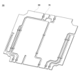
- FIG. 2 is a perspective view showing an example of a lead frame.
- the lead frame 35 has a surface on which a plurality of circuit patterns (later circuit patterns 30) are formed, and a convex bridge 31 connecting these.
- the lead frame 35 is formed using a metal plate with good electrical conductivity and thermal conductivity. For example, it is preferable to use an aluminum plate, a copper plate, etc., and a copper plate is more preferable from the viewpoint of low thermal resistance. preferable.
- the lead frame 35 may be surface-treated to prevent oxidation of copper, for example, nickel plating or solder plating. Further, the thickness of the lead frame 35 is adjusted as appropriate, but is preferably 0.3 to 1.0 mm, for example.
- the convex bridge 31 may be made of the same material as the circuit pattern 30 or a different material, but from the viewpoint of productivity, it is preferable that the convex bridge 31 be made of the same material. Moreover, it is preferable that the convex bridge 31 is integrally molded with the circuit pattern 30. There are a plurality of convex bridges 31, and the directions in which they straddle each other are parallel to each other. That is, the convex bridges are oriented in the same direction.
- the convex bridge 31 of this embodiment is formed as follows. First, a metal plate that is the material of the lead frame 35 is bent at a portion that will become the convex bridge 31. At this time, the degree of curvature is the same as the thickness of the metal plate. Thereafter, a plurality of independent circuit patterns 30 are formed by pressing and punching, thereby obtaining a lead frame 35 as shown in FIG. 2. In this embodiment, by making the connecting portion protrude above the circuit pattern 30, the convex bridge 31 can be removed together with a part of the sealing resin 40 in step 4, and production efficiency can be improved.
- the connecting portion of this embodiment then becomes a convex bridge 31.
- the connecting portion may be of a known type, but preferably has a length of 0.5 to 2 mm and a width of 0.5 to 2 mm, for example. Further, it is preferable that the connecting portions be provided in parallel directions to each other so that batch molding and batch processing can be performed.
- the lead frame 35 is placed on the insulating layer 20 by a known method with the convex bridge 31 facing upward.
- a sealing resin 40 is embedded between the circuits forming the circuit pattern 30.
- the resin composition is filled between the circuits using a method selected such as a transfer molding method, a compression molding method, or an injection molding method. bury it.
- the sealing resin 40 may be buried so as to cover the entire convex bridge 31, insulating layer 20, and circuit pattern 30.
- Step 4 A part of the sealing resin 40 and the convex bridge 31 are removed by polishing to match the height of the circuit pattern 30, thereby exposing the upper surface of the circuit pattern 30 (FIG. 1(c)). This allows the top surface of the sealing resin 40 and the top surface of the circuit pattern 30 to be flush with each other while eliminating the convex bridge 31, thereby increasing productivity.
- known methods can be used for the removal, polishing or cutting, for example, is preferable. Specifically, mechanical polishing (diamond bite, grindstone, buff, polishing roll, etc.) or chemical mechanical polishing (CMP) can be used. Further, by appropriately adjusting the polishing conditions, the height of the convex portion on the circuit pattern 30 of the circuit board with heat sink 50 can be adjusted.
- the semiconductor device 100 of this embodiment includes a heat sink 10, an insulating layer 20 laminated on one surface of the heat sink 10, and a circuit pattern 30 disposed on the insulating layer 20.
- a first sealing body 41 (cured product of sealing resin 40) is embedded between the circuits constituting the circuit pattern 30 and is configured such that its upper surface is substantially flush with the upper surface of the circuit pattern 30;
- the semiconductor chip 81 includes a semiconductor chip 81 mounted on the circuit pattern 30 exposed on the upper surface of the sealing resin 40, and a second sealing body 42 (hardened product of the second sealing resin) that covers the semiconductor chip 81. There is an interface between the sealing body 41 and the second sealing body 42. Further, the semiconductor chip 81 is connected to the lead frame 35 via a wire 83.
- the interface between the first sealed body 41 and the second sealed body 42 is created when the first sealed body 41 and the second sealed body 42 are obtained by different processes and then joined. It is a boundary.
- the interface may be visible, but is not limited to being visible. In this embodiment, the interface is a substantially horizontal surface.
- the second sealing body 42 can be obtained using a known sealing resin material.
- the first sealing body 41 and the second sealing body 42 may be formed of different resin materials, or may be formed of the same material, but may be formed of different resin materials. It is preferable.
- the linear expansion coefficient of the first sealing body 41 (cured product of the first sealing resin: 175°C for 3 minutes) at 40°C to 80°C is ⁇ 1 (ppm/°C)
- the second sealing body When the linear expansion coefficient of 42 (cured product of second sealing resin: 175°C for 3 minutes) at 40°C to 80°C is ⁇ 2 (ppm/°C), ( ⁇ 1/ ⁇ 2) is 0.7 to 1. It is preferably 5, and more preferably 0.8 to 1.2.
- the smaller the difference between ⁇ 1 and ⁇ 2 the more effectively the interface peeling caused by the difference in linear expansion coefficient between the first sealing body 41 and the second sealing body 42 and the peeling from the circuit pattern 30 due to warping can be prevented. It can be suppressed.
- ⁇ 1 and ⁇ 2 are adjusted as appropriate depending on the structure of the semiconductor module and the thickness of the sealing resin portion, but each is preferably 8 to 20 ppm/°C, more preferably 12 to 18 ppm/°C. preferable. Thereby, warping and peeling within the semiconductor device 100 can be suppressed, and reliability can be improved.
- FIG. 3 is a cross-sectional view schematically showing a method for manufacturing the semiconductor device 100 of this embodiment.
- the method for manufacturing the semiconductor device 100 includes the steps of using a circuit board 50 with a heat sink, mounting a semiconductor chip 81 on the circuit pattern 30 exposed on the circuit board 50 with a heat sink, and mounting the semiconductor chip 81 with a second sealing resin. and sealing to form a second sealed body 42.
- Known methods can be used for both the process of mounting the semiconductor chip 81 and the process of forming the second sealing body 42.
- the semiconductor device 100 of this embodiment uses the circuit board 50 with a heat sink, processability, manufacturing stability, positional accuracy, etc. are improved, and reliability, durability, etc. can be improved.
- the circuit board 51 with a heat sink and the heat sink 10 of the semiconductor device 101 may have fins 12. Details will be explained below.
- the heat sink 10 may include a flat base plate 11 and a plurality of fins 12 protruding from the surface of the base plate 11 opposite to the insulating layer 20 side.
- the flat base plate 11 and the fins 12 may be joined by a known method, or may be integrally molded.
- the thickness of the base plate 11 can be set as appropriate depending on the application, but is preferably 0.2 to 1.5 mm, for example. Further, by setting the thickness of the base plate 11 to 0.5 to 1.5 times the thickness of the circuit pattern 30, warping of the entire circuit board 51 with a heat sink can be suppressed and adhesion can be easily improved.
- the heat sink 10 includes a plurality of fins 12 erected from one surface of the base plate 11, thereby increasing the surface area of the heat sink 10 and increasing heat dissipation efficiency. Further, the plurality of fins 12 are flush with each other. Since the height of the plurality of fins 12 is uniform and the upper surface of the fin 12 is flat, a surface can be formed, so that the circuit board 51 with a heat sink can be manufactured stably.
- the shape of the fins 12 is not particularly limited, but may be, for example, a polygonal columnar shape such as a square or hexagonal column, or a cylindrical shape.
- the above-mentioned quadrangular columnar shape may be a columnar shape having a square cross-sectional shape, a rectangular columnar shape, a rhomboidal columnar shape, a parallelogram-shaped columnar shape, or the like.
- the above-mentioned cylindrical shape may have a circular, elliptical, oval, etc. cross-sectional shape.
- the number of the plurality of fins 12 is not particularly limited, and is appropriately set from the viewpoints of usage, mechanical strength, etc.
- the shapes of the plurality of fins 12 may be the same, different, or only partially different.
- the arrangement of the plurality of fins 12 is not particularly limited, it is preferable that the region surrounded by the outline connecting the outer ends of the fins 12 be included in the region covered by the insulating layer 20 of the base plate 11. . Further, it is preferable that the base plate 11 does not have the fins 12 at the outer peripheral end thereof. By doing so, it is possible to improve adhesion while maintaining mechanical strength against pressurization during the manufacturing process of the circuit board with heat sink 51.
- the distance between the plurality of fins 12 is not particularly limited, but is preferably 0.5 to 2.0 mm.
- the cutting of the fins 12 can be performed efficiently, and mechanical strength can be maintained against pressure during the manufacturing process of the circuit board with heat sink 50. It becomes like this. Further, by setting the interval between the fins 12 to 2.0 mm or less, the heat dissipation performance of the heat sink 10 can be further improved.
- Example> A metal base material (copper foil with a thickness of 500 ⁇ m) was punched to produce a lead frame having a circuit pattern and a convex bridge. Using a low-pressure transfer molding machine, the obtained lead frame was injected with a resin composition for semiconductor encapsulation (thermosetting resin, curing agent, (inorganic filler, curing accelerator, coupling agent, etc.) was used to seal and mold (first sealing body). Subsequently, a part of the sealing body and the convex portion of the convex bridge were polished using a diamond cutting tool to expose the upper surface of the circuit pattern.
- a resin composition for semiconductor encapsulation thermosetting resin, curing agent, (inorganic filler, curing accelerator, coupling agent, etc.
Landscapes
- Cooling Or The Like Of Semiconductors Or Solid State Devices (AREA)
Abstract
ヒートシンク付回路基板(50)の製造方法は、以下の工程を含む。ヒートシンク(10)の一方の面上に絶縁層(20)を積層する工程と、絶縁層(20)上に、独立した複数の回路パターン(30)と、隣接する回路パターン(30)間を跨ぐように設けられた凸状ブリッジ(31)と、を備えるリードフレーム(35)を配置する工程と、回路パターン(30)間に封止樹脂(40)を埋設する工程と、封止樹脂(40)の一部および凸状ブリッジ(31)を削除して回路パターン(30)の上面を露出させる工程。
Description
本発明は、ヒートシンク付回路基板およびその製造方法、ならびにこれを用いた半導体装置およびその製造方法に関する。
パワー半導体素子を伝熱用の金属回路基板に設けたパワーモジュールの市場が拡大している。そのようなパワーモジュールでは、高い放熱性を実現するために各種の技術が提案されている。回路を構成する導体層と大容量ヒートシンクの一面とが絶縁層を介して一体化されたヒートシンク付き回路基板が知られている(例えば、特許文献1)。
一方で、半導体素子等を含むパワーモジュールの電気配線にリードフレームを用いることが知られている。リードフレームには、高密度化に対応すべく独立した複数のパターンが形成され、隣接するパターンを連結する連結部を備えられている。特許文献2には、リードフレームのパターン間の連結部を打ち抜く工程において、連結部周辺のパターン部に発生する反りを抑制する点から、互いに独立した複数のパターンと、隣接するパターン間の間隙部に充填され該隣接するパターン相互を接続する樹脂接合材とを備えるリードフレームが開示されている。
近年、電気・電子機器等の発展に伴いヒートシンク付回路基板はますます注目されている。本発明者は、新たなヒートシンク付回路基板の製造方法に着目し、リードフレームにおいて隣接する回路パターン間を連結する連結部を、回路パターンの上面から突出させ、跨ぐように設け、その後、回路パターン間に封止樹脂を埋設させた後、連結部を削除しつつ回路パターンの上面を露出させるという方法を新規に考案した。これにより、密着性が良好なヒートシンク付回路基板を安定的、効率よく製造できる。
本発明によれば、以下のヒートシンク付回路基板の製造方法、ヒートシンク付回路基板、およびこれを用いた半導体装置の製造方法が提供される。
[1] ヒートシンクの一方の面上に絶縁層を積層する工程と、
前記絶縁層上に、独立した複数の回路パターンと、隣接する前記回路パターン間を跨ぐように設けられた凸状ブリッジと、を備えるリードフレームを配置する工程と、
前記回路パターン間に第1の封止樹脂を埋設する工程と、
前記第1の封止樹脂の一部および前記凸状ブリッジを削除して前記回路パターンの上面を露出させる工程と、
を含む、ヒートシンク付回路基板の製造方法。
[2] [1]に記載のヒートシンク付回路基板の製造方法であって、
前記凸状ブリッジは、前記回路パターンと一体成形されている、ヒートシンク付回路基板の製造方法。
[3] [1]または[2]に記載のヒートシンク付回路基板の製造方法であって、
前記凸状ブリッジが複数であって、互いに跨ぐ方向が平行である、ヒートシンク付回路基板の製造方法。
[4] [1]乃至[3]いずれか一つに記載のヒートシンク付回路基板の製造方法であって、
前記回路パターンの上面を露出させる前記工程は、研磨または切削により行われる、ヒートシンク付回路基板の製造方法。
[5] [1]乃至[4]いずれか一つに記載のヒートシンク付回路基板の製造方法であって、
前記第1の封止樹脂を埋設する前記工程は、トランスファーモールド成形法、コンプレッションモールド成形法及びインジェクション成形法からなる群より選択される方法が用いられる、ヒートシンク付回路基板の製造方法。
[6] [1]乃至[5]いずれか一つに記載のヒートシンク付回路基板の製造方法によって得られたヒートシンク付回路基板を用いた半導体装置の製造方法であって、
露出している前記回路パターンの上面に半導体チップを実装する工程と、
前記半導体チップを第2の封止樹脂により封止する工程と、
を含む、半導体装置の製造方法。
[7] [6]に記載の半導体装置の製造方法であって、
前記第1の封止樹脂の硬化物(175℃3分)の40℃~80℃における線膨張係数α1(ppm/℃)と第2の封止樹脂の硬化物(175℃3分)の40℃~80℃における線膨張係数α2(ppm/℃)との比(α1/α2)が0.7~1.5である、半導体装置の製造方法。
[8] [7]に記載の半導体装置の製造方法であって、
前記線膨張係数α1が8~20ppm/℃である、半導体装置の製造方法。
[9] ヒートシンクの一方の面上に設けられた絶縁層と、
前記絶縁層上に設けられた回路パターンと、
前記回路パターン間に埋設された第1の封止樹脂と、
を備える、ヒートシンク付回路基板であって、
前記回路パターンの上面と前記第1の封止樹脂の上面が略面一であり、
前記回路パターンの少なくとも表面の一部に高さ10nm以上の凸部を有する、ヒートシンク付回路基板。
[10] [9]に記載のヒートシンク付回路基板であって、
前記凸部は、前記回路パターンの外縁より1mm以内に形成されている、ヒートシンク付回路基板。
[11] [9]または[10]に記載のヒートシンク付回路基板であって、
前記回路パターンの外周端縁に囲まれる領域は、前記ヒートシンク上の前記絶縁層に覆われる領域に内包されている、ヒートシンク付回路基板。
[12] [9]乃至[11]いずれか一つに記載のヒートシンク付回路基板であって、
前記絶縁層の外周端縁は、前記第1の封止樹脂により覆われている、ヒートシンク付回路基板。
[13] [9]乃至[12]いずれか一つに記載のヒートシンク付回路基板であって、
前記絶縁層に含まれる熱硬化性樹脂が、ジシクロペンタジエン骨格を有するエポキシ樹脂、ビフェニル骨格を有するエポキシ樹脂、アダマンタン骨格を有するエポキシ樹脂、フェノールアラルキル骨格を有するエポキシ樹脂、ビフェニルアラルキル骨格を有するエポキシ樹脂、ナフタレンアラルキル骨格を有するエポキシ樹脂、ナフタレン骨格を有するエポキシ樹脂、メトキシナフタレンアラルキル骨格を有するエポキシ樹脂、およびシアネート樹脂から選択される1種または2種以上である、ヒートシンク付回路基板。
[14] [9]乃至[13]いずれか一つに記載のヒートシンク付回路基板であって、
前記絶縁層が窒化ホウ素粒子を含む、ヒートシンク付回路基板。
[15] [9]乃至[14]いずれか一つに記載のヒートシンク付回路基板であって、
前記絶縁層のBステージにおける比重が1.0~2.0である、ヒートシンク付回路基板。
[16] [9]乃至[15]いずれか一つに記載のヒートシンク付回路基板であって、
前記ヒートシンクは、銅、アルミニウムの中から選ばれる少なくとも1種である、ヒートシンク付回路基板。
[17] [9]乃至[16]いずれか一つに記載のヒートシンク付回路基板であって、
前記ヒートシンクは、前記ベース板の前記絶縁層とは反対側の面から突出する複数のフィンをさらに有する、ヒートシンク付回路基板。
前記絶縁層上に、独立した複数の回路パターンと、隣接する前記回路パターン間を跨ぐように設けられた凸状ブリッジと、を備えるリードフレームを配置する工程と、
前記回路パターン間に第1の封止樹脂を埋設する工程と、
前記第1の封止樹脂の一部および前記凸状ブリッジを削除して前記回路パターンの上面を露出させる工程と、
を含む、ヒートシンク付回路基板の製造方法。
[2] [1]に記載のヒートシンク付回路基板の製造方法であって、
前記凸状ブリッジは、前記回路パターンと一体成形されている、ヒートシンク付回路基板の製造方法。
[3] [1]または[2]に記載のヒートシンク付回路基板の製造方法であって、
前記凸状ブリッジが複数であって、互いに跨ぐ方向が平行である、ヒートシンク付回路基板の製造方法。
[4] [1]乃至[3]いずれか一つに記載のヒートシンク付回路基板の製造方法であって、
前記回路パターンの上面を露出させる前記工程は、研磨または切削により行われる、ヒートシンク付回路基板の製造方法。
[5] [1]乃至[4]いずれか一つに記載のヒートシンク付回路基板の製造方法であって、
前記第1の封止樹脂を埋設する前記工程は、トランスファーモールド成形法、コンプレッションモールド成形法及びインジェクション成形法からなる群より選択される方法が用いられる、ヒートシンク付回路基板の製造方法。
[6] [1]乃至[5]いずれか一つに記載のヒートシンク付回路基板の製造方法によって得られたヒートシンク付回路基板を用いた半導体装置の製造方法であって、
露出している前記回路パターンの上面に半導体チップを実装する工程と、
前記半導体チップを第2の封止樹脂により封止する工程と、
を含む、半導体装置の製造方法。
[7] [6]に記載の半導体装置の製造方法であって、
前記第1の封止樹脂の硬化物(175℃3分)の40℃~80℃における線膨張係数α1(ppm/℃)と第2の封止樹脂の硬化物(175℃3分)の40℃~80℃における線膨張係数α2(ppm/℃)との比(α1/α2)が0.7~1.5である、半導体装置の製造方法。
[8] [7]に記載の半導体装置の製造方法であって、
前記線膨張係数α1が8~20ppm/℃である、半導体装置の製造方法。
[9] ヒートシンクの一方の面上に設けられた絶縁層と、
前記絶縁層上に設けられた回路パターンと、
前記回路パターン間に埋設された第1の封止樹脂と、
を備える、ヒートシンク付回路基板であって、
前記回路パターンの上面と前記第1の封止樹脂の上面が略面一であり、
前記回路パターンの少なくとも表面の一部に高さ10nm以上の凸部を有する、ヒートシンク付回路基板。
[10] [9]に記載のヒートシンク付回路基板であって、
前記凸部は、前記回路パターンの外縁より1mm以内に形成されている、ヒートシンク付回路基板。
[11] [9]または[10]に記載のヒートシンク付回路基板であって、
前記回路パターンの外周端縁に囲まれる領域は、前記ヒートシンク上の前記絶縁層に覆われる領域に内包されている、ヒートシンク付回路基板。
[12] [9]乃至[11]いずれか一つに記載のヒートシンク付回路基板であって、
前記絶縁層の外周端縁は、前記第1の封止樹脂により覆われている、ヒートシンク付回路基板。
[13] [9]乃至[12]いずれか一つに記載のヒートシンク付回路基板であって、
前記絶縁層に含まれる熱硬化性樹脂が、ジシクロペンタジエン骨格を有するエポキシ樹脂、ビフェニル骨格を有するエポキシ樹脂、アダマンタン骨格を有するエポキシ樹脂、フェノールアラルキル骨格を有するエポキシ樹脂、ビフェニルアラルキル骨格を有するエポキシ樹脂、ナフタレンアラルキル骨格を有するエポキシ樹脂、ナフタレン骨格を有するエポキシ樹脂、メトキシナフタレンアラルキル骨格を有するエポキシ樹脂、およびシアネート樹脂から選択される1種または2種以上である、ヒートシンク付回路基板。
[14] [9]乃至[13]いずれか一つに記載のヒートシンク付回路基板であって、
前記絶縁層が窒化ホウ素粒子を含む、ヒートシンク付回路基板。
[15] [9]乃至[14]いずれか一つに記載のヒートシンク付回路基板であって、
前記絶縁層のBステージにおける比重が1.0~2.0である、ヒートシンク付回路基板。
[16] [9]乃至[15]いずれか一つに記載のヒートシンク付回路基板であって、
前記ヒートシンクは、銅、アルミニウムの中から選ばれる少なくとも1種である、ヒートシンク付回路基板。
[17] [9]乃至[16]いずれか一つに記載のヒートシンク付回路基板であって、
前記ヒートシンクは、前記ベース板の前記絶縁層とは反対側の面から突出する複数のフィンをさらに有する、ヒートシンク付回路基板。
本発明によれば、信頼性に優れたヒートシンク付回路基板およびその製造方法を提供できる。
以下、本発明の実施形態について、図面を参照しつつ、詳細に説明する。
すべての図面において、同様な構成要素には同様の符号を付し、適宜説明を省略する。なお、図面はあくまで説明用のものである。図面中の各部材の形状や寸法比などは、必ずしも現実の物品と対応するものではない。
すべての図面において、同様な構成要素には同様の符号を付し、適宜説明を省略する。なお、図面はあくまで説明用のものである。図面中の各部材の形状や寸法比などは、必ずしも現実の物品と対応するものではない。
本明細書中、数値範囲の説明における「a~b」との表記は、特に断らない限り、a以上b以下のことを表す。例えば、「1~5質量%」とは「1質量%以上5質量%以下」を意味する。
<ヒートシンク付回路基板>
本実施形態に係るヒートシンク付回路基板50は、図1(c)に示されるように、ヒートシンク10の一方の面上に設けられた絶縁層20と、絶縁層20上に設けられた回路パターン30と、回路パターン30間に埋設された封止樹脂40(第1の封止樹脂)と、を備える。また回路パターン30の上面と封止樹脂40の上面が略面一であり、回路パターン30の少なくとも表面の一部に高さ10nm以上の凸部を有する。
本実施形態のヒートシンク付回路基板50は回路パターン30の少なくとも表面の一部に高さ10nm以上の凸部を有することで、ヒートシンク付回路基板50を用いて後述の半導体装置100を製造した際の第2の封止樹脂との密着性を高めることができる。その結果、半導体装置100の信頼性を高めることができる。
本実施形態に係るヒートシンク付回路基板50は、図1(c)に示されるように、ヒートシンク10の一方の面上に設けられた絶縁層20と、絶縁層20上に設けられた回路パターン30と、回路パターン30間に埋設された封止樹脂40(第1の封止樹脂)と、を備える。また回路パターン30の上面と封止樹脂40の上面が略面一であり、回路パターン30の少なくとも表面の一部に高さ10nm以上の凸部を有する。
本実施形態のヒートシンク付回路基板50は回路パターン30の少なくとも表面の一部に高さ10nm以上の凸部を有することで、ヒートシンク付回路基板50を用いて後述の半導体装置100を製造した際の第2の封止樹脂との密着性を高めることができる。その結果、半導体装置100の信頼性を高めることができる。
当該凸部の高さは10nm以上であり、好ましくは100nm以上である。一方、凸部の高さの上限は、好ましくは3000nm以下であり、より好ましくは2000nm以下である。凸部の高さを上記下限値以上とすることにより、密着性を高めやすくなる。一方、凸部の高さを上記上限値以下とすることにより、ヒートシンク付回路基板50の上面を平滑にし、製造安定性を向上しやすくなる。
本実施形態において、凸部は、走査電子顕微鏡の断面の撮影像において凸部の両端の凹部の極小点を結んだ線分と垂直に延ばした長さが10nm以上となるものとする。
当該凸部の数は特に限定されず、生産性と回路パターン30の目的等に応じて適宜調整されるが、例えば、独立した一つの回路パターン30に対して2~10個であることが好ましい。
当該凸部は、独立した一つの回路パターン30の外縁よりも内側でありつつも、できるだけ外縁に近いことが好ましい。具体的には、独立した一つの回路パターン30の外縁より1mm以内に形成されていることが好ましい。
また、隣接する独立した回路パターン30間において、一方の回路パターン30の外縁近傍に設けられた凸部と、他方の回路パターン30の外縁近傍に設けられた凸部は互いに対向する位置であることが好ましい。
なお、本実施形態の凸部は、後述する製造方法を用いることで形成することができる。また、凸部の高さは、研磨条件を調整する等公知の方法により調整することができる。
また、隣接する独立した回路パターン30間において、一方の回路パターン30の外縁近傍に設けられた凸部と、他方の回路パターン30の外縁近傍に設けられた凸部は互いに対向する位置であることが好ましい。
なお、本実施形態の凸部は、後述する製造方法を用いることで形成することができる。また、凸部の高さは、研磨条件を調整する等公知の方法により調整することができる。
以下、ヒートシンク付回路基板50の各構成の詳細を説明する。
[回路パターン]
回路パターン30は、後述するリードフレーム35の一部をエッチング等して形成された回路である。回路パターン30は、絶縁層20を介してヒートシンク10上に形成される。本実施形態において、ヒートシンク付回路基板50はそれぞれ独立した複数の回路パターン30を備える。
回路パターン30は、後述するリードフレーム35の一部をエッチング等して形成された回路である。回路パターン30は、絶縁層20を介してヒートシンク10上に形成される。本実施形態において、ヒートシンク付回路基板50はそれぞれ独立した複数の回路パターン30を備える。
また、平面視における回路パターン30の配置は適宜設定されるが、回路パターン30の最外周端縁に囲まれる領域は、絶縁層20に覆われる領域に内包されていることが好ましい。すなわち、すべての回路パターン30は、絶縁層20の領域内、すなわち絶縁層20上に配置されることが好ましい。これにより、回路パターン30と絶縁層20とをより確実に密着できる。
[封止樹脂]
封止樹脂40は、回路パターン30を構成する回路間を充填するために用いられる。封止樹脂40としては、半導体装置の封止樹脂として知られる公知のものを用いることができる。例えば、封止樹脂40は、熱硬化性樹脂、無機充填剤、硬化剤、硬化促進剤、およびカップリング剤等を含む封止用樹脂組成物を用いて得られる。封止樹脂40は、後述の絶縁層20とは異なる樹脂材料を用いて構成される。
封止樹脂40は、回路パターン30を構成する回路間を充填するために用いられる。封止樹脂40としては、半導体装置の封止樹脂として知られる公知のものを用いることができる。例えば、封止樹脂40は、熱硬化性樹脂、無機充填剤、硬化剤、硬化促進剤、およびカップリング剤等を含む封止用樹脂組成物を用いて得られる。封止樹脂40は、後述の絶縁層20とは異なる樹脂材料を用いて構成される。
ヒートシンク付回路基板50の封止樹脂40は、Bステージ状態、Cステージ状態のいずれであってもよく、トランスファー、コンプレッション等の成形後は半硬化であることが好ましい。
上記の熱硬化性樹脂としては、好ましくはエポキシ樹脂が挙げられる。エポキシ樹脂としては、具体的には、ビフェニル型エポキシ樹脂、ビスフェノールA型エポキシ樹脂、ビスフェノールF型エポキシ樹脂、テトラメチルビスフェノールF型エポキシ樹脂等のビスフェノール型エポキシ樹脂、スチルベン型エポキシ樹脂、ハイドロキノン型エポキシ樹脂等の結晶性エポキシ樹脂;クレゾールノボラック型エポキシ樹脂、フェノールノボラック型エポキシ樹脂、ナフトールノボラック型エポキシ樹脂等のノボラック型エポキシ樹脂;フェニレン骨格含有フェノールアラルキル型エポキシ樹脂、ビフェニレン骨格含有フェノールアラルキル型エポキシ樹脂、フェニレン骨格含有ナフトールアラルキル型エポキシ樹脂、アルコキシナフタレン骨格含有フェノールアラルキルエポキシ樹脂等のアラルキル型エポキシ樹脂;トリフェノールメタン型エポキシ樹脂、アルキル変性トリフェノールメタン型エポキシ樹脂等の3官能型エポキシ樹脂;ジシクロペンタジエン変性フェノール型エポキシ樹脂、テルペン変性フェノール型エポキシ樹脂等の変性フェノール型エポキシ樹脂;トリアジン核含有エポキシ樹脂等の複素環含有エポキシ樹脂が挙げられる。これらは1種類を単独で用いてもよく、2種類以上を組み合わせて用いてもよい。
上記の無機充填剤としては、たとえば、タルク、焼成クレー、未焼成クレー、マイカ、ガラスなどのケイ酸塩;酸化チタン、アルミナ、ベーマイト、シリカなどの酸化物;炭酸カルシウム、炭酸マグネシウム、ハイドロタルサイトなどの炭酸塩;水酸化アルミニウム、水酸化マグネシウム、水酸化カルシウムなどの水酸化物;硫酸バリウム、硫酸カルシウム、亜硫酸カルシウムなどの硫酸塩または亜硫酸塩;ホウ酸亜鉛、メタホウ酸バリウム、ホウ酸アルミニウム、ホウ酸カルシウム、ホウ酸ナトリウムなどのホウ酸塩;窒化アルミニウム、窒化ホウ素、窒化ケイ素、窒化炭素などの窒化物;チタン酸ストロンチウム、チタン酸バリウムなどのチタン酸塩などが挙げられる。これらは、1種単独で用いてもよいし、2種以上を併用してもよい。
上記の硬化剤としては、熱硬化性樹脂と反応して硬化させるものであればとくに限定されないが、たとえば、エチレンジアミン、トリメチレンジアミン、テトラメチレンジアミン、および、ヘキサメチレンジアミン等の炭素数2~20の直鎖脂肪族ジアミン、ならびに、メタフェニレンジアミン、パラフェニレンジアミン、パラキシレンジアミン、4,4’-ジアミノジフェニルメタン、4,4’-ジアミノジフェニルプロパン、4,4’-ジアミノジフェニルエーテル、4,4’-ジアミノジフェニルスルホン、4,4’-ジアミノジシクロヘキサン、ビス(4-アミノフェニル)フェニルメタン、1,5-ジアミノナフタレン、メタキシレンジアミン、パラキシレンジアミン、1,1-ビス(4-アミノフェニル)シクロヘキサン、ジシアノジアミド等のアミン類;アニリン変性レゾール樹脂、ジメチルエーテルレゾール樹脂等のレゾール型フェノール樹脂;フェノールノボラック樹脂、クレゾールノボラック樹脂、tert-ブチルフェノールノボラック樹脂、ノニルフェノールノボラック樹脂等のノボラック型フェノール樹脂;フェニレン骨格含有フェノールアラルキル樹脂、ビフェニレン骨格含有フェノールアラルキル樹脂等のフェノールアラルキル樹脂;ナフタレン骨格やアントラセン骨格のような縮合多環構造を有するフェノール樹脂;ポリパラオキシスチレン等のポリオキシスチレン;ヘキサヒドロ無水フタル酸(HHPA)、メチルテトラヒドロ無水フタル酸(MTHPA)等の脂環族酸無水物、無水トリメリット酸(TMA)、無水ピロメリット酸(PMDA)、ベンゾフェノンテトラカルボン酸(BTDA)等の芳香族酸無水物等を含む酸無水物等;ポリサルファイド、チオエステル、チオエーテル等のポリメルカプタン化合物;イソシアネートプレポリマー、ブロック化イソシアネート等のイソシアネート化合物;カルボン酸含有ポリエステル樹脂等の有機酸類が挙げられる。これらは1種類を単独で用いてもよく、2種類以上を組み合わせて用いてもよい。
上記の硬化促進剤としては、たとえば、有機ホスフィン、テトラ置換ホスホニウム化合物、ホスホベタイン化合物、ホスフィン化合物とキノン化合物との付加物、または、ホスホニウム化合物とシラン化合物との付加物等のリン原子含有化合物;1,8-ジアザビシクロ(5,4,0)ウンデセン-7、イミダゾール等のアミジン系化合物;ベンジルジメチルアミン等の3級アミン、アミジニウム塩、またはアンモニウム塩等の窒素原子含有化合物;フェノール、ビスフェノールA、ノニルフェノール、2,3-ジヒドロキシナフタレン等のフェノール化合物等が挙げられる。また、上記有機ホスフィンとしては、トリフェニルホスフィン、トリ-p-トリルホスフィン、テトラフェニルホスホニウム・テトラフェニルボレート、トリフェニルホスフィン・トリフェニルボラン、1,2-ビス-(ジフェニルホスフィノ)エタン等が挙げられる。
上記のカップリング剤としては、たとえばエポキシシラン、メルカプトシラン、アミノシラン、アルキルシラン、ウレイドシラン、ビニルシラン等の各種シラン系化合物、チタン系化合物、アルミニウムキレート類、アルミニウム/ジルコニウム系化合物等の公知のカップリング剤を用いることができる。
また、上記成分の他に、たとえば、上記エポキシ樹脂以外のフェノール樹脂、エポキシ樹脂、不飽和ポリエステル樹脂、メラミン樹脂、およびポリウレタン等熱硬化性樹脂;カーボンブラック等の着色剤;天然ワックス、合成ワックス、高級脂肪酸もしくはその金属塩類、パラフィン、酸化ポリエチレン等の離型剤;ハイドロタルサイト等のイオン捕捉剤;シリコーンオイル、シリコーンゴム等の低応力剤;水酸化アルミニウム等の難燃剤;酸化防止剤等の各種添加剤を含むことができる。
かかる封止用樹脂組成物は、公知の方法により得られるものであり、例えば、上述した成分を、超音波分散方式、高圧衝突式分散方式、高速回転分散方式、ビーズミル方式、高速せん断分散方式、または自転公転式分散方式などの各種混合機を用いて溶剤中に溶解、混合、撹拌することによりワニス状の組成物として調製することができる。
[絶縁層]
絶縁層20は、回路パターン30とヒートシンク10との間に配置されることにより、回路パターン30に通電される電気がヒートシンク10側に漏れないよう絶縁するために用いられる。
また、絶縁層20は、良好な熱伝導性を有し、放熱性に優れる。絶縁層20の厚み方向の熱伝導率(25℃)は、本実施形態の樹脂組成物(P1)の硬化体の熱伝導率(25℃)よりも高いことが好ましく、具体的には、7.5W/m・K以上であることが好ましい。
また、絶縁層20は、封止樹脂40(第1の封止樹脂)とは異なる工程により形成されるものである。すなわち、絶縁層20と封止樹脂40(第1の封止樹脂)との間に界面が存在する。
また、絶縁層20の外周端部は封止樹脂40により覆われている。これにより、ヒートシンク付回路基板50の信頼性を向上しやすくなる。
絶縁層20は、回路パターン30とヒートシンク10との間に配置されることにより、回路パターン30に通電される電気がヒートシンク10側に漏れないよう絶縁するために用いられる。
また、絶縁層20は、良好な熱伝導性を有し、放熱性に優れる。絶縁層20の厚み方向の熱伝導率(25℃)は、本実施形態の樹脂組成物(P1)の硬化体の熱伝導率(25℃)よりも高いことが好ましく、具体的には、7.5W/m・K以上であることが好ましい。
また、絶縁層20は、封止樹脂40(第1の封止樹脂)とは異なる工程により形成されるものである。すなわち、絶縁層20と封止樹脂40(第1の封止樹脂)との間に界面が存在する。
また、絶縁層20の外周端部は封止樹脂40により覆われている。これにより、ヒートシンク付回路基板50の信頼性を向上しやすくなる。
絶縁層20は、樹脂材料から構成されることが好ましく、熱硬化性樹脂と、窒化ホウ素粒子とを含む材料から構成されることがより好ましい。これにより、良好な熱伝導性、および絶縁性が得られる。また、絶縁層20は、ヒートシンク付回路基板50の製造過程において圧力がかかることによって、窒化ホウ素粒子が分散し熱伝導性を効率的に向上することができるとともに、密着性を高めることができる。
上記の熱硬化性樹脂としては、ジシクロペンタジエン骨格を有するエポキシ樹脂、ビフェニル骨格を有するエポキシ樹脂、アダマンタン骨格を有するエポキシ樹脂、フェノールアラルキル骨格を有するエポキシ樹脂、ビフェニルアラルキル骨格を有するエポキシ樹脂、ナフタレンアラルキル骨格を有するエポキシ樹脂、ナフタレン骨格を有するエポキシ樹脂、メトキシナフタレンアラルキル骨格を有するエポキシ樹脂、およびシアネート樹脂から選択される一種または二種以上が挙げられる。これにより、窒化ホウ素粒子の分散性を向上させやすくなる。
上記のシアネート樹脂としては、シアネートエステル樹脂を用いることができる。
シアネートエステル樹脂としては、具体的には、ビスフェノールAジシアネート、ポリフェノールシアネート(オリゴ(3-メチレン-1,5-フェニレンシアネート)、4,4'-メチレンビス(2,6-ジメチルフェニルシアネート)、4,4'-エチリデンジフェニルジシアネート、ヘキサフルオロビスフェノールAジシアネート、2,2-ビス(4-シアネート)フェニルプロパン、1,1-ビス(4-シアネートフェニルメタン)、ビス(4-シアネート-3,5-ジメチルフェニル)メタン、1,3-ビス(4-シアネートフェニル-1-(メチルエチリデン))ベンゼン、ビス(4-シアネートフェニル)チオエーテル、ビス(4-シアネートフェニル)エーテルなどの2官能シアネート樹脂;フェノールノボラック、クレゾールノボラック、ジシクロペンタジエン構造含有フェノール樹脂などから誘導される多官能シアネート樹脂;上記例示したシアネートエステル樹脂の一部がトリアジン化したプレポリマーなどが挙げられる。
ここで、シアネートエステル樹脂の市販品としては、例えば、ロンザジャパン社製のPT30、BA230、DT-4000、DT-7000などを用いることができる。
シアネートエステル樹脂としては、具体的には、ビスフェノールAジシアネート、ポリフェノールシアネート(オリゴ(3-メチレン-1,5-フェニレンシアネート)、4,4'-メチレンビス(2,6-ジメチルフェニルシアネート)、4,4'-エチリデンジフェニルジシアネート、ヘキサフルオロビスフェノールAジシアネート、2,2-ビス(4-シアネート)フェニルプロパン、1,1-ビス(4-シアネートフェニルメタン)、ビス(4-シアネート-3,5-ジメチルフェニル)メタン、1,3-ビス(4-シアネートフェニル-1-(メチルエチリデン))ベンゼン、ビス(4-シアネートフェニル)チオエーテル、ビス(4-シアネートフェニル)エーテルなどの2官能シアネート樹脂;フェノールノボラック、クレゾールノボラック、ジシクロペンタジエン構造含有フェノール樹脂などから誘導される多官能シアネート樹脂;上記例示したシアネートエステル樹脂の一部がトリアジン化したプレポリマーなどが挙げられる。
ここで、シアネートエステル樹脂の市販品としては、例えば、ロンザジャパン社製のPT30、BA230、DT-4000、DT-7000などを用いることができる。
熱硬化性樹脂の含有量は、絶縁層20を構成する材料(固形分)全量に対して、1質量%以上30質量%以下の範囲が好ましく、5質量%以上28質量%以下の範囲がより好ましい。
窒化ホウ素粒子は、一次粒子が凝集した凝集粒子であることが好ましい。窒化ホウ素粒子の一次粒子は、板状、鱗片状、または球状であり得、好ましくは鱗片状である。本実施形態で用いられる窒化ホウ素粒子は、鱗片状窒化ホウ素の凝集粒子であることが好ましい。これにより、窒化ホウ素粒子が配列し、熱伝導性を向上しやすくなる。
鱗片状(または板状)の窒化ホウ素の一次粒子は、長手方向長さ(鱗片の厚み方向に対する直交方向における最大長さ)の平均が、例えば、1~100μm、好ましくは、3~90μmである。また、窒化ホウ素粒子の長手方向長さの平均は、5μm以上、好ましくは、10μm以上、さらに好ましくは、20μm以上、とりわけ好ましくは、30μm以上、最も好ましくは、40μm以上であり、通常、例えば、100μm以下、好ましくは、90μm以下である。
また、鱗片状窒化ホウ素の一次粒子の厚み(鱗片の厚み方向長さ、つまり、粒子の短手方向長さ)の平均は、例えば、0.01~20μm、好ましくは、0.1~15μmである。
また、鱗片状窒化ホウ素の一次粒子のアスペクト比(長手方向長さ/厚み)は、例えば、2~10000、好ましくは、10~5000である。
なお、光散乱法によって測定される平均1次粒子径は、動的光散乱式粒度分布測定装置にて測定される体積平均粒子径である。窒化ホウ素粒子の光散乱法によって測定される平均1次粒子径が上記範囲に満たないと、絶縁層20が脆くなり、取扱性が低下する場合がある。
窒化ホウ素粒子の市販品として、具体的には、例えば、モメンティブ・パフォーマンス・マテリアルズ・ジャパン社製の「PT」シリーズ(例えば、「PT-110」など)、昭和電工社製の「ショービーエヌUHP」シリーズ(例えば、「ショービーエヌUHP-1」など)などが挙げられる。
窒化ホウ素粒子の含有量は、絶縁層20を構成する材料(固形分)全量に対して、60質量%以上80質量%以下の量であり、より好ましくは、65質量%以上75質量%以下の量である。
また、窒化ホウ素粒子の体積基準の含有割合は、絶縁層20を構成する材料(固形分)の全積に対して、50~70体積%であることが好ましく、55~65体積%であることがより好ましい。
また、窒化ホウ素粒子の体積基準の含有割合は、絶縁層20を構成する材料(固形分)の全積に対して、50~70体積%であることが好ましく、55~65体積%であることがより好ましい。
絶縁層20を構成する材料としては、上記熱伝導性樹脂、窒化ホウ素粒子以外の成分をさらに含んでもよい。
例えば、熱硬化性樹脂としてエポキシ樹脂を用いる場合、硬化剤を用いることが好ましい。硬化剤としては、硬化触媒またはフェノール系硬化剤を用いることが好ましい。
硬化触媒としては、たとえばナフテン酸亜鉛、ナフテン酸コバルト、オクチル酸スズ、オクチル酸コバルト、ビスアセチルアセトナートコバルト(II)、トリスアセチルアセトナートコバルト(III)等の有機金属塩;トリエチルアミン、トリブチルアミン、1,4-ジアザビシクロ[2.2.2]オクタン等の3級アミン類;2-フェニル-4-メチルイミダゾール、2-エチル-4-メチルイミダゾール、2,4-ジエチルイミダゾール、2-フェニル-4-メチル-5-ヒドロキシイミダゾール、2-フェニル-4,5-ジヒドロキシメチルイミダゾール等のイミダゾール類;トリフェニルホスフィン、トリ-p-トリルホスフィン、テトラフェニルホスホニウム・テトラフェニルボレート、トリフェニルホスフィン・トリフェニルボラン、1,2-ビス-(ジフェニルホスフィノ)エタン等の有機リン化合物;フェノール、ビスフェノールA、ノニルフェノール等のフェノール化合物;酢酸、安息香酸、サリチル酸、p-トルエンスルホン酸等の有機酸;等、またはこの混合物が挙げられる。
硬化触媒を用いる場合、その含有量は、絶縁層20を構成する材料(固形分)全量に対し、0.001質量部以上1質量部以下が好ましい。
また、フェノール系硬化剤としては、フェノールノボラック樹脂、クレゾールノボラック樹脂、ナフトールノボラック樹脂、アミノトリアジンノボラック樹脂、ノボラック樹脂、トリスフェニルメタン型のフェノールノボラック樹脂等のノボラック型フェノール樹脂;テルペン変性フェノール樹脂、ジシクロペンタジエン変性フェノール樹脂等の変性フェノール樹脂;フェニレン骨格及び/又はビフェニレン骨格を有するフェノールアラルキル樹脂、フェニレン骨格及び/又はビフェニレン骨格を有するナフトールアラルキル樹脂等のアラルキル型樹脂;ビスフェノールA、ビスフェノールF等のビスフェノール化合物;レゾール型フェノール樹脂等が挙げられ、これらは1種類を単独で用いても2種類以上を併用してもよい。
フェノール系硬化剤の含有量は、絶縁層20を構成する材料(固形分)全量に対し、0.1質量%以上30質量%以下が好ましく、0.3質量%以上15質量%以下がより好ましい。
フェノール系硬化剤の含有量は、絶縁層20を構成する材料(固形分)全量に対し、0.1質量%以上30質量%以下が好ましく、0.3質量%以上15質量%以下がより好ましい。
絶縁層20を構成する材料は、さらに、レベリング剤、カップリング剤、酸化防止剤等を含んでもよい。
レベリング剤としては、アクリル系共重合物等が挙げられる。レベリング剤は、絶縁層20を構成する材料(固形分)全量に対し、2質量%以下の量で使用することが好ましく、0.01質量%以上1.0質量%以下の量で使用することがより好ましい。
カップリング剤としては、エポキシシランカップリング剤、カチオニックシランカップリング剤、アミノシランカップリング剤、チタネート系カップリング剤およびシリコーンオイル型カップリング剤等が使用できる。
カップリング剤の配合量は、窒化ホウ素粒子100質量部に対して、0.1質量部以上10質量部以下が好ましく、特に0.5質量部以上7質量部以下が好ましい。
カップリング剤の配合量は、窒化ホウ素粒子100質量部に対して、0.1質量部以上10質量部以下が好ましく、特に0.5質量部以上7質量部以下が好ましい。
本実施形態の絶縁層20を構成する材料(固形分)は、上述した熱硬化性樹脂、窒化ホウ素粒子、その他の成分、および溶媒を上述の割合で配合し、公知の方法により撹拌混合することにより調製できる。
溶媒としては、アセトン、メチルエチルケトンなどケトン、酢酸エチルなどのエステル、N,N-ジメチルホルムアミドなどのアミドなどの有機溶媒が挙げられる。また、溶媒として、水、メタノール、エタノール、プロパノール、イソプロパノールなどのアルコールなどの水系溶媒も挙げられる。
本実施形態の絶縁層20は、Bステージ状態のシート状に成形して作製することができる。すなわち、絶縁層20は、ヒートシンク付回路基板50の製造過程において、ヒートシンク10および回路パターン30と加熱加圧一体化される際に、完全硬化する。
たとえば、基材上にワニス状の上記材料を塗布した後、これを熱処理して乾燥することによりシート状にすることができる。基材としては、たとえば放熱部材やリードフレーム、剥離可能なキャリア材等を構成する金属箔が挙げられるが、ヒートシンク10上に直接塗布してもよい。
また、塗布膜を乾燥するための熱処理は、たとえば80~150℃、5分~1時間の条件において行われる。
絶縁層20の厚みは、たとえば60μm以上500μm以下とすることができる。
たとえば、基材上にワニス状の上記材料を塗布した後、これを熱処理して乾燥することによりシート状にすることができる。基材としては、たとえば放熱部材やリードフレーム、剥離可能なキャリア材等を構成する金属箔が挙げられるが、ヒートシンク10上に直接塗布してもよい。
また、塗布膜を乾燥するための熱処理は、たとえば80~150℃、5分~1時間の条件において行われる。
絶縁層20の厚みは、たとえば60μm以上500μm以下とすることができる。
本実施形態において、Bステージ状態のシート状の絶縁層20の比重は1.0~2.0であることが好ましい。これにより、ヒートシンク付回路基板50の製造過程において、より適切に加圧でき、ヒートシンク10および回路パターン30との密着性を高めやすくなる。
[ヒートシンク]
ヒートシンク10は、回路パターン30等において発生した熱を外部に放出する機能を有する。
ヒートシンク10の厚みは、用途に応じて適宜設定できるが、例えば、0.2~5mmであることが好ましい。
ヒートシンク10は、回路パターン30等において発生した熱を外部に放出する機能を有する。
ヒートシンク10の厚みは、用途に応じて適宜設定できるが、例えば、0.2~5mmであることが好ましい。
ヒートシンク10は、銅、アルミニウムの中から選ばれる少なくとも1種であることが好ましく、熱伝導性・加工性等を向上する観点からは銅であることがより好ましい。
<ヒートシンク付回路基板の製造方法>
次に、図1を用いて、本実施形態のヒートシンク付回路基板50の製造方法について説明する。
本実施形態のヒートシンク付回路基板50の製造方法は、以下の工程を含む。
[工程1]ヒートシンク10の一方の面上に絶縁層20を積層する工程。
[工程2]絶縁層20上に、独立した複数の回路パターン30と、隣接する回路パターン30間を跨ぐように設けられた凸状ブリッジ31と、を備えるリードフレーム35を配置する工程。
[工程3]回路パターン30間に封止樹脂40を埋設する工程。
[工程4]封止樹脂40の一部および凸状ブリッジ31を削除して回路パターン30の上面を露出させる工程。
次に、図1を用いて、本実施形態のヒートシンク付回路基板50の製造方法について説明する。
本実施形態のヒートシンク付回路基板50の製造方法は、以下の工程を含む。
[工程1]ヒートシンク10の一方の面上に絶縁層20を積層する工程。
[工程2]絶縁層20上に、独立した複数の回路パターン30と、隣接する回路パターン30間を跨ぐように設けられた凸状ブリッジ31と、を備えるリードフレーム35を配置する工程。
[工程3]回路パターン30間に封止樹脂40を埋設する工程。
[工程4]封止樹脂40の一部および凸状ブリッジ31を削除して回路パターン30の上面を露出させる工程。
これにより、回路パターン30の少なくとも表面の一部に高さ10nm以上の凸部を有する、ヒートシンク付回路基板50が得られる。すなわち、ヒートシンク付回路基板50は、隣接する回路パターン30間を跨ぐように設けられた凸状ブリッジ31を封止樹脂40とともに削除することで、当該凸部をえることができる。
以下、各工程の詳細を説明する。
以下、各工程の詳細を説明する。
[工程1]
ヒートシンク10としては、上述したものを用いることができる。次に、ヒートシンク10の一方の面上に公知の方法で絶縁層20を積層する。
ヒートシンク10としては、上述したものを用いることができる。次に、ヒートシンク10の一方の面上に公知の方法で絶縁層20を積層する。
[工程2]
まず、図1(a)に示されるような、独立した複数の回路パターン30と、隣接する回路パターン30間を跨ぐように設けられた凸状ブリッジ31と、を備えるリードフレーム35を準備する。ここで、リードフレーム35について詳述する。
まず、図1(a)に示されるような、独立した複数の回路パターン30と、隣接する回路パターン30間を跨ぐように設けられた凸状ブリッジ31と、を備えるリードフレーム35を準備する。ここで、リードフレーム35について詳述する。
(リードフレーム)
図2は、リードフレームの一例を示す斜視図である。図2に示されるように、リードフレーム35は複数の回路パターンを形成する面(のちの回路パターン30)と、これらを繋ぐ凸状ブリッジ31とを有している。
リードフレーム35は、電気伝導性及び熱伝導性の良好な金属板を用いて形成されるが、例えば、アルミニウム板、銅板などを用いることが好ましく、低熱抵抗化の点から銅板であることがより好ましい。リードフレーム35は、銅などの酸化防止の点から表面処理が施されていてもよく、例えば、ニッケルめっきやはんだめっき処理がされていてもよい。
また、リードフレーム35の厚さは、適宜調整されるが、例えば0.3~1.0mmであることが好適である。
図2は、リードフレームの一例を示す斜視図である。図2に示されるように、リードフレーム35は複数の回路パターンを形成する面(のちの回路パターン30)と、これらを繋ぐ凸状ブリッジ31とを有している。
リードフレーム35は、電気伝導性及び熱伝導性の良好な金属板を用いて形成されるが、例えば、アルミニウム板、銅板などを用いることが好ましく、低熱抵抗化の点から銅板であることがより好ましい。リードフレーム35は、銅などの酸化防止の点から表面処理が施されていてもよく、例えば、ニッケルめっきやはんだめっき処理がされていてもよい。
また、リードフレーム35の厚さは、適宜調整されるが、例えば0.3~1.0mmであることが好適である。
凸状ブリッジ31は、回路パターン30と同一材料であっても、異なる材料であってもよいが、生産性の点から、同一材料であることが好ましい。また、凸状ブリッジ31は、回路パターン30と一体成形されていることが好ましい。
凸状ブリッジ31が複数であって、互いに跨ぐ方向が平行である。すなわち、凸状ブリッジは互いに同じ方向になっている。
凸状ブリッジ31が複数であって、互いに跨ぐ方向が平行である。すなわち、凸状ブリッジは互いに同じ方向になっている。
本実施形態の凸状ブリッジ31は、次のようにして形成される。
まず、リードフレーム35の材料となる金属板に対し、凸状ブリッジ31となる部分に曲げ加工を行う。この時、湾曲の程度は金属板の厚みと同じ程度とする。その後、プレスし、打ち抜き加工を施すことによって、独立した複数の回路パターン30を形成することで、図2に示すようなリードフレーム35が得られる。
本実施形態において、連結部を回路パターン30上に突出させることで、工程4において、封止樹脂40の一部とともに凸状ブリッジ31を削除することができ、生産効率を高めることができる。
まず、リードフレーム35の材料となる金属板に対し、凸状ブリッジ31となる部分に曲げ加工を行う。この時、湾曲の程度は金属板の厚みと同じ程度とする。その後、プレスし、打ち抜き加工を施すことによって、独立した複数の回路パターン30を形成することで、図2に示すようなリードフレーム35が得られる。
本実施形態において、連結部を回路パターン30上に突出させることで、工程4において、封止樹脂40の一部とともに凸状ブリッジ31を削除することができ、生産効率を高めることができる。
本実施形態の連結部は、その後凸状ブリッジ31となる。連結部は、公知のものとすることができるが、例えば、長さ0.5~2mm、幅0.5~2mmとすることが好ましい。また、一括成形、一括加工できるよう、連結部は互いに平行な方向に設けられることが好ましい。
次に、リードフレーム35を凸状ブリッジ31が上側となるようにして絶縁層20上に公知の方法で配置する。
[工程3]
次に、図1(b)に示されるように、回路パターン30を構成する回路間に封止樹脂40を埋設する。たとえば、封止樹脂40用の樹脂組成物を用い、トランスファーモールド成形法、コンプレッションモールド成形法及びインジェクション成形法など選択される方法を用いて、回路間に樹脂組成物を充填し、封止樹脂40を埋設する。
このとき、封止樹脂40は、凸状ブリッジ31と絶縁層20及び回路パターン30全体を覆うようにして、埋設されてもよい。
次に、図1(b)に示されるように、回路パターン30を構成する回路間に封止樹脂40を埋設する。たとえば、封止樹脂40用の樹脂組成物を用い、トランスファーモールド成形法、コンプレッションモールド成形法及びインジェクション成形法など選択される方法を用いて、回路間に樹脂組成物を充填し、封止樹脂40を埋設する。
このとき、封止樹脂40は、凸状ブリッジ31と絶縁層20及び回路パターン30全体を覆うようにして、埋設されてもよい。
[工程4]
封止樹脂40の一部および凸状ブリッジ31を研磨により削除して、回路パターン30の高さに合わせることで、回路パターン30の上面を露出させる(図1(c))。これにより、凸状ブリッジ31を削除しつつ、封止樹脂40の上面と回路パターン30の上面を面一にすることができ、生産性を高めることができる。
削除する方法は、公知の方法を用いることができるが、たとえば、研磨または切削であることが好ましい。具体的には、機械的研磨(ダイヤモンドバイト、砥石、バフ、研磨ロール等)や、化学的機械研磨(CMP)を用いることができる。
また、研磨条件を適宜調整することにより、ヒートシンク付回路基板50の回路パターン30上の凸部の高さを調整することができる。
封止樹脂40の一部および凸状ブリッジ31を研磨により削除して、回路パターン30の高さに合わせることで、回路パターン30の上面を露出させる(図1(c))。これにより、凸状ブリッジ31を削除しつつ、封止樹脂40の上面と回路パターン30の上面を面一にすることができ、生産性を高めることができる。
削除する方法は、公知の方法を用いることができるが、たとえば、研磨または切削であることが好ましい。具体的には、機械的研磨(ダイヤモンドバイト、砥石、バフ、研磨ロール等)や、化学的機械研磨(CMP)を用いることができる。
また、研磨条件を適宜調整することにより、ヒートシンク付回路基板50の回路パターン30上の凸部の高さを調整することができる。
<半導体装置>
図3(b)に示すように、本実施形態の半導体装置100は、ヒートシンク10と、ヒートシンク10の一方の面上に積層された絶縁層20と、絶縁層20上に配置された回路パターン30と、回路パターン30を構成する回路間に埋設され、上面が回路パターン30の上面と略面一となるように構成された第1封止体41(封止樹脂40の硬化物)と、封止樹脂40の上面に露出する回路パターン30上に搭載された半導体チップ81と、半導体チップ81を覆う第2封止体42(第2の封止樹脂の硬化物)と、を備え、第1封止体41と第2封止体42との間に界面がある。
また、半導体チップ81は、リードフレーム35とワイヤ83を介して接続されている。
図3(b)に示すように、本実施形態の半導体装置100は、ヒートシンク10と、ヒートシンク10の一方の面上に積層された絶縁層20と、絶縁層20上に配置された回路パターン30と、回路パターン30を構成する回路間に埋設され、上面が回路パターン30の上面と略面一となるように構成された第1封止体41(封止樹脂40の硬化物)と、封止樹脂40の上面に露出する回路パターン30上に搭載された半導体チップ81と、半導体チップ81を覆う第2封止体42(第2の封止樹脂の硬化物)と、を備え、第1封止体41と第2封止体42との間に界面がある。
また、半導体チップ81は、リードフレーム35とワイヤ83を介して接続されている。
第1封止体41と第2封止体42との間の界面とは、第1封止体41と第2封止体42とが異なる工程によって得られたのちに接合されることで生じる境界である。界面は、目視できるものであってもよく、目視できるものに限られない。本実施形態において当該界面は略水平面である。
第2封止体42は、公知の封止樹脂材料を用いて得ることができる。第1封止体41と、第2封止体42とは、異なる樹脂材料により形成されていてもよく、同じ材料で形成されたものであってもよいが、異なる樹脂材料により形成されていることが好ましい。
第2封止体42は、公知の封止樹脂材料を用いて得ることができる。第1封止体41と、第2封止体42とは、異なる樹脂材料により形成されていてもよく、同じ材料で形成されたものであってもよいが、異なる樹脂材料により形成されていることが好ましい。
本実施形態において第1封止体41(第1の封止樹脂の硬化物:175℃3分)の40℃~80℃における線膨張係数をα1(ppm/℃)とし、第2封止体42(第2の封止樹脂の硬化物:175℃3分)の40℃~80℃における線膨張係数をα2(ppm/℃)としたとき、(α1/α2)が0.7~1.5であることが好ましく、0.8~1.2であることがより好ましい。すなわち、α1とα2の差が小さくなるほど、第1封止体41と第2封止体42との線膨張係数の差によって生じる界面剥離や、反りによる回路パターン30との剥離等を効果的に抑制できる。
本実施形態において、α1、α2は、半導体モジュールの構造や封止樹脂部分の厚みによって適宜調整されるが、それぞれ8~20ppm/℃であることが好ましく、12~18ppm/℃であることがより好ましい。これにより、半導体装置100内での反りや剥離を抑制し、信頼性を向上できる。
<半導体装置の製造方法>
図3は、本実施形態の半導体装置100の製造方法を模式的に示す断面図である。
半導体装置100の製造方法は、ヒートシンク付回路基板50を用い、ヒートシンク付回路基板50に露出する回路パターン30上に、半導体チップ81を実装する工程と、半導体チップ81を第2の封止樹脂により封止し、第2の封止体42を形成する工程と、を含む。
半導体チップ81を実装する工程および第2の封止体42を形成する工程はいずれも公知の方法を用いることができる。
図3は、本実施形態の半導体装置100の製造方法を模式的に示す断面図である。
半導体装置100の製造方法は、ヒートシンク付回路基板50を用い、ヒートシンク付回路基板50に露出する回路パターン30上に、半導体チップ81を実装する工程と、半導体チップ81を第2の封止樹脂により封止し、第2の封止体42を形成する工程と、を含む。
半導体チップ81を実装する工程および第2の封止体42を形成する工程はいずれも公知の方法を用いることができる。
本実施形態の半導体装置100は、ヒートシンク付回路基板50を用いるものであるため、加工性、製造安定性、位置精度等が向上し、信頼性、耐久性などに優れることができる。
以上、図面を参照して本発明の実施形態について述べたが、これらは本発明の例示であり、上記以外の様々な構成を採用することもできる。
<変形例>
例えば、図4、5に示すように、ヒートシンク付回路基板51、半導体装置101のヒートシンク10はフィン12を有するものであってもよい。以下、詳細を説明する。
例えば、図4、5に示すように、ヒートシンク付回路基板51、半導体装置101のヒートシンク10はフィン12を有するものであってもよい。以下、詳細を説明する。
ヒートシンク10は、平板状のベース板11と、ベース板11の絶縁層20側とは反対側の面から突出する複数のフィン12とを備えてもよい。平板状のベース板11と、フィン12とは公知の方法で接合されたものであってもよく、一体成形されたものであってもよい。
ベース板11の厚みは、用途に応じて適宜設定できるが、例えば、0.2~1.5mmであることが好ましい。また、ベース板11の厚みを、回路パターン30の厚みの0.5~1.5倍とすることで、ヒートシンク付回路基板51全体の反りを抑制し、密着性を向上しやすくなる。
本実施形態において、ヒートシンク10は、ベース板11の一方の面から立設する複数のフィン12を備えることにより、ヒートシンク10の表面積を高め、放熱効率を高めることができる。また複数のフィン12は面一となっている。複数のフィン12の高さが均一であり、また、フィン12の上面は平坦であることで面を構成できるため、ヒートシンク付回路基板51の安定的に製造できるようになる。
フィン12の形状は特に限定されないが、例えば、四角、六角などの多角柱状、円柱状であってもよい。また、上記の四角柱状には、断面における断面形状が正方形を呈する柱状、長方形を呈する柱状、ひし形を呈する柱状、平行四辺形を呈する柱状等であってよい。上記の円柱状には、断面における断面形状が円形、楕円形及び長円形等であってもよい。
複数のフィン12の数は特に限定されず、用途、機械的強度等の観点から、適宜設定される。複数のフィン12の形状は、互いに同一であってもよく、異なっていてもよく、一部のみ異なるものであってもよい。
また、複数のフィン12の配置は、特に限定されないが、フィン12の外側端を結ぶ外郭線に囲まれる領域は、ベース板11の絶縁層20に覆われた領域に内包されていることが好ましい。また、ベース板11の外周端部にフィン12を有さないことが好ましい。
こうすることにより、ヒートシンク付回路基板51の製造過程における加圧に対して、機械的強度を保持しつつ、密着性を向上できる。
こうすることにより、ヒートシンク付回路基板51の製造過程における加圧に対して、機械的強度を保持しつつ、密着性を向上できる。
複数のフィン12同士の間隔は、特に限定されないが、0.5~2.0mmであることが好ましい。フィン12同士の間隔を0.5mm以上とすることにより、フィン12の切削加工を効率的に行うことができ、またヒートシンク付回路基板50の製造過程における押圧に対して、機械的強度を保持できるようになる。また、フィン12同士の間隔を2.0mm以下とすることにより、ヒートシンク10の放熱性能をより向上させることができる。
以下、本発明を実施例により説明するが、本発明はこれらに限定されるものではない。
<実施例>
金属基材(厚さ500μmの銅箔)を打ち抜き加工して、回路パターンおよび凸状ブリッジを有するリードフレームを作製した。
得られたリードフレームを、低圧トランスファー成形機を用いて、金型温度175℃、注入圧力10.0MPa、硬化時間2分の条件で半導体封止用樹脂組成物(熱硬化性樹脂、硬化剤、無機充填材、硬化促進剤、カップリング剤他)を用いて封止成形(第1封止体)した。続けて、ダイヤモンドバイトにより封止体の一部と凸状ブリッジの凸部を研磨して、回路パターンの上面を露出させた。回路パターンの上面をSEMにより観察したところ、複数の高さ10nm凸部が回路パターンの外縁で観察された。続けて、回路パターンの上面を覆うようにして上記と同じ半導体封止用樹脂組成物を用いて封止成形(第2封止体)し、半導体装置を得た。
第1封止体と第2封止体は良好に密着し、負荷を与えても、界面剥離は観察されなかった。
金属基材(厚さ500μmの銅箔)を打ち抜き加工して、回路パターンおよび凸状ブリッジを有するリードフレームを作製した。
得られたリードフレームを、低圧トランスファー成形機を用いて、金型温度175℃、注入圧力10.0MPa、硬化時間2分の条件で半導体封止用樹脂組成物(熱硬化性樹脂、硬化剤、無機充填材、硬化促進剤、カップリング剤他)を用いて封止成形(第1封止体)した。続けて、ダイヤモンドバイトにより封止体の一部と凸状ブリッジの凸部を研磨して、回路パターンの上面を露出させた。回路パターンの上面をSEMにより観察したところ、複数の高さ10nm凸部が回路パターンの外縁で観察された。続けて、回路パターンの上面を覆うようにして上記と同じ半導体封止用樹脂組成物を用いて封止成形(第2封止体)し、半導体装置を得た。
第1封止体と第2封止体は良好に密着し、負荷を与えても、界面剥離は観察されなかった。
この出願は、2022年4月28日に出願された日本出願特願2022-075376号を基礎とする優先権を主張し、その開示の全てをここに取り込む。
10 ヒートシンク
11 ベース板
12 フィン
20 絶縁層
30 回路パターン
31 凸状ブリッジ
35 リードフレーム
40 封止樹脂
41 第1封止体
42 第2封止体
50 ヒートシンク付回路基板
51 ヒートシンク付回路基板
81 半導体チップ
83 ワイヤ
100 半導体装置
101 半導体装置
11 ベース板
12 フィン
20 絶縁層
30 回路パターン
31 凸状ブリッジ
35 リードフレーム
40 封止樹脂
41 第1封止体
42 第2封止体
50 ヒートシンク付回路基板
51 ヒートシンク付回路基板
81 半導体チップ
83 ワイヤ
100 半導体装置
101 半導体装置
Claims (17)
- ヒートシンクの一方の面上に絶縁層を積層する工程と、
前記絶縁層上に、独立した複数の回路パターンと、隣接する前記回路パターン間を跨ぐように設けられた凸状ブリッジと、を備えるリードフレームを配置する工程と、
前記回路パターン間に第1の封止樹脂を埋設する工程と、
前記第1の封止樹脂の一部および前記凸状ブリッジを削除して前記回路パターンの上面を露出させる工程と、
を含む、ヒートシンク付回路基板の製造方法。 - 請求項1に記載のヒートシンク付回路基板の製造方法であって、
前記凸状ブリッジは、前記回路パターンと一体成形されている、ヒートシンク付回路基板の製造方法。 - 請求項1または2に記載のヒートシンク付回路基板の製造方法であって、
前記凸状ブリッジが複数であって、互いに跨ぐ方向が平行である、ヒートシンク付回路基板の製造方法。 - 請求項1または2に記載のヒートシンク付回路基板の製造方法であって、
前記回路パターンの上面を露出させる前記工程は、研磨または切削により行われる、ヒートシンク付回路基板の製造方法。 - 請求項1または2に記載のヒートシンク付回路基板の製造方法であって、
前記第1の封止樹脂を埋設する前記工程は、トランスファーモールド成形法、コンプレッションモールド成形法及びインジェクション成形法からなる群より選択される方法が用いられる、ヒートシンク付回路基板の製造方法。 - 請求項1または2に記載のヒートシンク付回路基板の製造方法によって得られたヒートシンク付回路基板を用いた半導体装置の製造方法であって、
露出している前記回路パターンの上面に半導体チップを実装する工程と、
前記半導体チップを第2の封止樹脂により封止する工程と、
を含む、半導体装置の製造方法。 - 請求項6に記載の半導体装置の製造方法であって、
前記第1の封止樹脂の硬化物(175℃3分)の40℃~80℃における線膨張係数α1(ppm/℃)と第2の封止樹脂の硬化物(175℃3分)の40℃~80℃における線膨張係数α2(ppm/℃)との比(α1/α2)が0.7~1.5である、半導体装置の製造方法。 - 請求項7に記載の半導体装置の製造方法であって、
前記線膨張係数α1が8~20ppm/℃である、半導体装置の製造方法。 - ヒートシンクの一方の面上に設けられた絶縁層と、
前記絶縁層上に設けられた回路パターンと、
前記回路パターン間に埋設された第1の封止樹脂と、
を備える、ヒートシンク付回路基板であって、
前記回路パターンの上面と前記第1の封止樹脂の上面が略面一であり、
前記回路パターンの少なくとも表面の一部に高さ10nm以上の凸部を有する、ヒートシンク付回路基板。 - 請求項9に記載のヒートシンク付回路基板であって、
前記凸部は、前記回路パターンの外縁より1mm以内に形成されている、ヒートシンク付回路基板。 - 請求項9または10に記載のヒートシンク付回路基板であって、
前記回路パターンの外周端縁に囲まれる領域は、前記ヒートシンク上の前記絶縁層に覆われる領域に内包されている、ヒートシンク付回路基板。 - 請求項9または10に記載のヒートシンク付回路基板であって、
前記絶縁層の外周端縁は、前記第1の封止樹脂により覆われている、ヒートシンク付回路基板。 - 請求項9または10に記載のヒートシンク付回路基板であって、
前記絶縁層に含まれる熱硬化性樹脂が、ジシクロペンタジエン骨格を有するエポキシ樹脂、ビフェニル骨格を有するエポキシ樹脂、アダマンタン骨格を有するエポキシ樹脂、フェノールアラルキル骨格を有するエポキシ樹脂、ビフェニルアラルキル骨格を有するエポキシ樹脂、ナフタレンアラルキル骨格を有するエポキシ樹脂、ナフタレン骨格を有するエポキシ樹脂、メトキシナフタレンアラルキル骨格を有するエポキシ樹脂、およびシアネート樹脂から選択される1種または2種以上である、ヒートシンク付回路基板。 - 請求項9または10に記載のヒートシンク付回路基板であって、
前記絶縁層が窒化ホウ素粒子を含む、ヒートシンク付回路基板。 - 請求項9または10に記載のヒートシンク付回路基板であって、
前記絶縁層のBステージにおける比重が1.0~2.0である、ヒートシンク付回路基板。 - 請求項9または10に記載のヒートシンク付回路基板であって、
前記ヒートシンクは、銅、アルミニウムの中から選ばれる少なくとも1種である、ヒートシンク付回路基板。 - 請求項9または10に記載のヒートシンク付回路基板であって、
前記ヒートシンクは、前記ベース板の前記絶縁層とは反対側の面から突出する複数のフィンをさらに有する、ヒートシンク付回路基板。
Priority Applications (1)
| Application Number | Priority Date | Filing Date | Title |
|---|---|---|---|
| JP2023552266A JP7401037B1 (ja) | 2022-04-28 | 2023-04-17 | ヒートシンク付回路基板およびその製造方法、ならびにこれを用いた半導体装置およびその製造方法 |
Applications Claiming Priority (2)
| Application Number | Priority Date | Filing Date | Title |
|---|---|---|---|
| JP2022075376 | 2022-04-28 | ||
| JP2022-075376 | 2022-04-28 |
Publications (1)
| Publication Number | Publication Date |
|---|---|
| WO2023210420A1 true WO2023210420A1 (ja) | 2023-11-02 |
Family
ID=88518539
Family Applications (1)
| Application Number | Title | Priority Date | Filing Date |
|---|---|---|---|
| PCT/JP2023/015293 Ceased WO2023210420A1 (ja) | 2022-04-28 | 2023-04-17 | ヒートシンク付回路基板およびその製造方法、ならびにこれを用いた半導体装置およびその製造方法 |
Country Status (2)
| Country | Link |
|---|---|
| JP (1) | JP7401037B1 (ja) |
| WO (1) | WO2023210420A1 (ja) |
Citations (6)
| Publication number | Priority date | Publication date | Assignee | Title |
|---|---|---|---|---|
| JPH06216499A (ja) * | 1993-01-19 | 1994-08-05 | Toshiba Corp | 銅回路基板の製造方法 |
| JP2001057406A (ja) * | 1999-06-11 | 2001-02-27 | Matsushita Electric Ind Co Ltd | 放熱基板及びその製造方法 |
| WO2009110376A1 (ja) * | 2008-03-06 | 2009-09-11 | 三菱電機株式会社 | リードフレーム基板、半導体モジュール、及びリードフレーム基板の製造方法 |
| WO2013035716A1 (ja) * | 2011-09-07 | 2013-03-14 | 株式会社村田製作所 | モジュールの製造方法 |
| JP2017017239A (ja) * | 2015-07-03 | 2017-01-19 | 住友ベークライト株式会社 | 回路付き部材の製造方法、回路付き部材および電子部品実装部材 |
| JP2017224750A (ja) * | 2016-06-16 | 2017-12-21 | ローム株式会社 | 半導体装置およびその製造方法 |
-
2023
- 2023-04-17 WO PCT/JP2023/015293 patent/WO2023210420A1/ja not_active Ceased
- 2023-04-17 JP JP2023552266A patent/JP7401037B1/ja active Active
Patent Citations (6)
| Publication number | Priority date | Publication date | Assignee | Title |
|---|---|---|---|---|
| JPH06216499A (ja) * | 1993-01-19 | 1994-08-05 | Toshiba Corp | 銅回路基板の製造方法 |
| JP2001057406A (ja) * | 1999-06-11 | 2001-02-27 | Matsushita Electric Ind Co Ltd | 放熱基板及びその製造方法 |
| WO2009110376A1 (ja) * | 2008-03-06 | 2009-09-11 | 三菱電機株式会社 | リードフレーム基板、半導体モジュール、及びリードフレーム基板の製造方法 |
| WO2013035716A1 (ja) * | 2011-09-07 | 2013-03-14 | 株式会社村田製作所 | モジュールの製造方法 |
| JP2017017239A (ja) * | 2015-07-03 | 2017-01-19 | 住友ベークライト株式会社 | 回路付き部材の製造方法、回路付き部材および電子部品実装部材 |
| JP2017224750A (ja) * | 2016-06-16 | 2017-12-21 | ローム株式会社 | 半導体装置およびその製造方法 |
Also Published As
| Publication number | Publication date |
|---|---|
| JP7401037B1 (ja) | 2023-12-19 |
| JPWO2023210420A1 (ja) | 2023-11-02 |
Similar Documents
| Publication | Publication Date | Title |
|---|---|---|
| US11798863B2 (en) | Laminate and electronic device | |
| US11459443B2 (en) | Resin material, method for producing resin material, and laminate | |
| CN105323957A (zh) | 覆金属箔基板、电路基板和电子部件搭载基板 | |
| JP2025120356A (ja) | パワーモジュール | |
| US20160122503A1 (en) | Resin composition for thermally conductive sheet, base material-attached resin layer, thermally conductive sheet, and semiconductor device | |
| JP7424542B2 (ja) | ヒートシンク付回路基板およびその製造方法、ならびに半導体装置およびその製造方法 | |
| KR20230039710A (ko) | 파워 모듈 | |
| JP7568173B2 (ja) | 半導体装置 | |
| JP7401037B1 (ja) | ヒートシンク付回路基板およびその製造方法、ならびにこれを用いた半導体装置およびその製造方法 | |
| JP6536129B2 (ja) | 半導体装置及びそれを備えるパワーモジュール | |
| JPWO2016002891A1 (ja) | 熱伝導性シートおよび半導体装置 | |
| JP7589576B2 (ja) | 回路基板の製造方法 | |
| JP6579106B2 (ja) | 熱伝導性シートおよび半導体装置 | |
| WO2025262832A1 (ja) | ヒートシンク付回路基板およびその製造方法 | |
| JP4075268B2 (ja) | 回路基板の製造方法 | |
| JP2024054495A (ja) | 半導体装置製造方法および構造体 | |
| JP6635034B2 (ja) | 半導体装置 | |
| JP2024135038A (ja) | 樹脂組成物、半導体装置、ヒートシンク付回路基板 | |
| TW202136469A (zh) | 導熱性片、積層體、及半導體裝置 | |
| JP2022088777A (ja) | 熱伝導性樹脂組成物、熱伝導性シート、および金属ベース基板 | |
| WO2015163055A1 (ja) | 金属ベース基板、金属ベース基板の製造方法、金属ベース回路基板および電子装置 | |
| JP2024136642A (ja) | 基板および半導体装置 | |
| WO2024063088A1 (ja) | ヒートシンク付回路基板およびヒートシンク付回路基板の製造方法 | |
| WO2015163056A1 (ja) | 金属ベース基板、金属ベース回路基板および電子装置 | |
| JP2022114048A (ja) | パワーモジュール |
Legal Events
| Date | Code | Title | Description |
|---|---|---|---|
| WWE | Wipo information: entry into national phase |
Ref document number: 2023552266 Country of ref document: JP |
|
| 121 | Ep: the epo has been informed by wipo that ep was designated in this application |
Ref document number: 23796163 Country of ref document: EP Kind code of ref document: A1 |
|
| NENP | Non-entry into the national phase |
Ref country code: DE |
|
| 122 | Ep: pct application non-entry in european phase |
Ref document number: 23796163 Country of ref document: EP Kind code of ref document: A1 |