WO2023210399A1 - プラズマ処理装置、電源システム及びプラズマ処理方法 - Google Patents
プラズマ処理装置、電源システム及びプラズマ処理方法 Download PDFInfo
- Publication number
- WO2023210399A1 WO2023210399A1 PCT/JP2023/015084 JP2023015084W WO2023210399A1 WO 2023210399 A1 WO2023210399 A1 WO 2023210399A1 JP 2023015084 W JP2023015084 W JP 2023015084W WO 2023210399 A1 WO2023210399 A1 WO 2023210399A1
- Authority
- WO
- WIPO (PCT)
- Prior art keywords
- power
- supply
- time
- peak
- level
- Prior art date
- Legal status (The legal status is an assumption and is not a legal conclusion. Google has not performed a legal analysis and makes no representation as to the accuracy of the status listed.)
- Ceased
Links
Images


Classifications
-
- H—ELECTRICITY
- H01—ELECTRIC ELEMENTS
- H01J—ELECTRIC DISCHARGE TUBES OR DISCHARGE LAMPS
- H01J37/00—Discharge tubes with provision for introducing objects or material to be exposed to the discharge, e.g. for the purpose of examination or processing thereof
- H01J37/32—Gas-filled discharge tubes
- H01J37/32009—Arrangements for generation of plasma specially adapted for examination or treatment of objects, e.g. plasma sources
- H01J37/32082—Radio frequency generated discharge
- H01J37/32091—Radio frequency generated discharge the radio frequency energy being capacitively coupled to the plasma
-
- H—ELECTRICITY
- H01—ELECTRIC ELEMENTS
- H01J—ELECTRIC DISCHARGE TUBES OR DISCHARGE LAMPS
- H01J37/00—Discharge tubes with provision for introducing objects or material to be exposed to the discharge, e.g. for the purpose of examination or processing thereof
- H01J37/32—Gas-filled discharge tubes
- H01J37/32009—Arrangements for generation of plasma specially adapted for examination or treatment of objects, e.g. plasma sources
- H01J37/32082—Radio frequency generated discharge
- H01J37/32137—Radio frequency generated discharge controlling of the discharge by modulation of energy
- H01J37/32146—Amplitude modulation, includes pulsing
-
- C—CHEMISTRY; METALLURGY
- C23—COATING METALLIC MATERIAL; COATING MATERIAL WITH METALLIC MATERIAL; CHEMICAL SURFACE TREATMENT; DIFFUSION TREATMENT OF METALLIC MATERIAL; COATING BY VACUUM EVAPORATION, BY SPUTTERING, BY ION IMPLANTATION OR BY CHEMICAL VAPOUR DEPOSITION, IN GENERAL; INHIBITING CORROSION OF METALLIC MATERIAL OR INCRUSTATION IN GENERAL
- C23C—COATING METALLIC MATERIAL; COATING MATERIAL WITH METALLIC MATERIAL; SURFACE TREATMENT OF METALLIC MATERIAL BY DIFFUSION INTO THE SURFACE, BY CHEMICAL CONVERSION OR SUBSTITUTION; COATING BY VACUUM EVAPORATION, BY SPUTTERING, BY ION IMPLANTATION OR BY CHEMICAL VAPOUR DEPOSITION, IN GENERAL
- C23C16/00—Chemical coating by decomposition of gaseous compounds, without leaving reaction products of surface material in the coating, i.e. chemical vapour deposition [CVD] processes
- C23C16/44—Chemical coating by decomposition of gaseous compounds, without leaving reaction products of surface material in the coating, i.e. chemical vapour deposition [CVD] processes characterised by the method of coating
- C23C16/50—Chemical coating by decomposition of gaseous compounds, without leaving reaction products of surface material in the coating, i.e. chemical vapour deposition [CVD] processes characterised by the method of coating using electric discharges
- C23C16/505—Chemical coating by decomposition of gaseous compounds, without leaving reaction products of surface material in the coating, i.e. chemical vapour deposition [CVD] processes characterised by the method of coating using electric discharges using radio frequency discharges
- C23C16/509—Chemical coating by decomposition of gaseous compounds, without leaving reaction products of surface material in the coating, i.e. chemical vapour deposition [CVD] processes characterised by the method of coating using electric discharges using radio frequency discharges using internal electrodes
-
- H—ELECTRICITY
- H01—ELECTRIC ELEMENTS
- H01J—ELECTRIC DISCHARGE TUBES OR DISCHARGE LAMPS
- H01J37/00—Discharge tubes with provision for introducing objects or material to be exposed to the discharge, e.g. for the purpose of examination or processing thereof
- H01J37/32—Gas-filled discharge tubes
- H01J37/32009—Arrangements for generation of plasma specially adapted for examination or treatment of objects, e.g. plasma sources
- H01J37/32082—Radio frequency generated discharge
- H01J37/32174—Circuits specially adapted for controlling the RF discharge
- H01J37/32183—Matching circuits
-
- H—ELECTRICITY
- H01—ELECTRIC ELEMENTS
- H01J—ELECTRIC DISCHARGE TUBES OR DISCHARGE LAMPS
- H01J37/00—Discharge tubes with provision for introducing objects or material to be exposed to the discharge, e.g. for the purpose of examination or processing thereof
- H01J37/32—Gas-filled discharge tubes
- H01J37/32431—Constructional details of the reactor
- H01J37/32715—Workpiece holder
-
- H—ELECTRICITY
- H05—ELECTRIC TECHNIQUES NOT OTHERWISE PROVIDED FOR
- H05H—PLASMA TECHNIQUE; PRODUCTION OF ACCELERATED ELECTRICALLY-CHARGED PARTICLES OR OF NEUTRONS; PRODUCTION OR ACCELERATION OF NEUTRAL MOLECULAR OR ATOMIC BEAMS
- H05H1/00—Generating plasma; Handling plasma
- H05H1/24—Generating plasma
- H05H1/46—Generating plasma using applied electromagnetic fields, e.g. high frequency or microwave energy
-
- H—ELECTRICITY
- H10—SEMICONDUCTOR DEVICES; ELECTRIC SOLID-STATE DEVICES NOT OTHERWISE PROVIDED FOR
- H10P—GENERIC PROCESSES OR APPARATUS FOR THE MANUFACTURE OR TREATMENT OF DEVICES COVERED BY CLASS H10
- H10P14/00—Formation of materials, e.g. in the shape of layers or pillars
- H10P14/20—Formation of materials, e.g. in the shape of layers or pillars of semiconductor materials
- H10P14/29—Formation of materials, e.g. in the shape of layers or pillars of semiconductor materials characterised by the substrates
-
- H—ELECTRICITY
- H10—SEMICONDUCTOR DEVICES; ELECTRIC SOLID-STATE DEVICES NOT OTHERWISE PROVIDED FOR
- H10P—GENERIC PROCESSES OR APPARATUS FOR THE MANUFACTURE OR TREATMENT OF DEVICES COVERED BY CLASS H10
- H10P14/00—Formation of materials, e.g. in the shape of layers or pillars
- H10P14/60—Formation of materials, e.g. in the shape of layers or pillars of insulating materials
-
- H—ELECTRICITY
- H10—SEMICONDUCTOR DEVICES; ELECTRIC SOLID-STATE DEVICES NOT OTHERWISE PROVIDED FOR
- H10P—GENERIC PROCESSES OR APPARATUS FOR THE MANUFACTURE OR TREATMENT OF DEVICES COVERED BY CLASS H10
- H10P50/00—Etching of wafers, substrates or parts of devices
- H10P50/20—Dry etching; Plasma etching; Reactive-ion etching
- H10P50/24—Dry etching; Plasma etching; Reactive-ion etching of semiconductor materials
- H10P50/242—Dry etching; Plasma etching; Reactive-ion etching of semiconductor materials of Group IV materials
-
- H—ELECTRICITY
- H01—ELECTRIC ELEMENTS
- H01J—ELECTRIC DISCHARGE TUBES OR DISCHARGE LAMPS
- H01J2237/00—Discharge tubes exposing object to beam, e.g. for analysis treatment, etching, imaging
- H01J2237/32—Processing objects by plasma generation
- H01J2237/33—Processing objects by plasma generation characterised by the type of processing
- H01J2237/332—Coating
- H01J2237/3321—CVD [Chemical Vapor Deposition]
Definitions
- the present disclosure relates to a plasma processing apparatus, a power supply system, and a plasma processing method.
- Patent Document 1 provides a method of etching a SiOC-based low-k film or the like using a SiC film as a base film.
- the power of the RF power source is slowed up to a second power value and then placed in a power modulation mode.
- the DC voltage of the variable DC power supply is slowed down. By slowing down either of these, damage to the wafer or power supply can be reduced.
- the present disclosure provides a technique that can suppress plasma load fluctuations.
- a plasma processing chamber a substrate support section provided in the plasma processing chamber and on which a substrate is placed, a gas supply section supplying a processing gas to the plasma processing chamber, and the an RF power source that supplies pulsed RF power to the plasma processing chamber and/or the substrate support to generate plasma of the processing gas; and a control device that controls the supply of the pulsed RF power.
- control device is configured such that an increasing function of the power level from the start point of supply of the pulsed RF power to the point of peak occurrence is a downwardly convex function, and/or the control device
- a plasma processing apparatus is provided in which the RF power source is controlled so that a decreasing function of the power level from a peak end point to a supply end point is a downwardly convex function.
- plasma load fluctuations can be suppressed.
- FIG. 1 is a diagram showing an example of a plasma processing apparatus according to an embodiment. The figure which shows the transition sequence example of the continuous wave of RF electric power, and a pulse wave of a reference example.
- FIG. 3 is a diagram showing an example of a transition sequence between a continuous wave and a pulse wave of RF power according to the embodiment.
- FIG. 7 is a diagram showing an increasing function of the power level of an RF pulse in a reference example during a ramp-up period.
- FIG. 4 is a diagram illustrating an increasing function of the power level of the RF pulse for an embodiment of the ramp-up period.
- FIG. 6 is a diagram illustrating a decreasing function of the power level of an RF pulse for an embodiment of a ramp-down period.
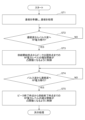
- 1 is a flowchart illustrating an example of a plasma processing method according to an embodiment.
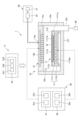
- FIG. 1 is a diagram for explaining a configuration example of a capacitively coupled plasma processing apparatus.
- the plasma processing apparatus 1 is a capacitively coupled plasma processing apparatus, and includes a plasma processing chamber 10, a gas supply section 20, a power supply 30, an exhaust system 40, and a control device 2. Further, the plasma processing apparatus 1 includes a substrate support section 11 and a gas introduction section. The gas inlet is configured to introduce at least one processing gas into the plasma processing chamber 10 .
- the gas introduction section includes a shower head 13.
- Substrate support 11 is arranged within plasma processing chamber 10 .
- the shower head 13 is arranged above the substrate support section 11 . In one embodiment, showerhead 13 forms at least a portion of the ceiling of plasma processing chamber 10 .
- the plasma processing chamber 10 has a plasma processing space 10s defined by a shower head 13, a side wall 10a of the plasma processing chamber 10, and a substrate support 11.
- the plasma processing chamber 10 has at least one gas supply port for supplying at least one processing gas to the plasma processing space 10s, and at least one gas exhaust port for discharging gas from the plasma processing space.
- Plasma processing chamber 10 is grounded.
- the shower head 13 and substrate support 11 are electrically insulated from the casing of the plasma processing chamber 10.
- the substrate support section 11 includes a main body section 111 and a ring assembly 112.
- the main body portion 111 has a central region 111a for supporting the substrate W and an annular region 111b for supporting the ring assembly 112.
- a wafer is an example of a substrate W.
- the annular region 111b of the main body 111 surrounds the central region 111a of the main body 111 in plan view.
- the substrate W is placed on the central region 111a of the main body 111, and the ring assembly 112 is placed on the annular region 111b of the main body 111 so as to surround the substrate W on the central region 111a of the main body 111. Therefore, the central region 111a is also called a substrate support surface for supporting the substrate W, and the annular region 111b is also called a ring support surface for supporting the ring assembly 112.
- the main body 111 includes a base 1110 and an electrostatic chuck 1111.
- Base 1110 includes a conductive member.
- the conductive member of the base 1110 can function as a bottom electrode.
- Electrostatic chuck 1111 is placed on base 1110.
- Electrostatic chuck 1111 includes a ceramic member 1111a and an electrostatic electrode 1111b disposed within ceramic member 1111a.
- Ceramic member 1111a has a central region 111a. In one embodiment, ceramic member 1111a also has an annular region 111b. Note that another member surrounding the electrostatic chuck 1111, such as an annular electrostatic chuck or an annular insulating member, may have the annular region 111b.
- ring assembly 112 may be placed on the annular electrostatic chuck or the annular insulation member, or may be placed on both the electrostatic chuck 1111 and the annular insulation member.
- at least one RF/DC electrode coupled to an RF (Radio Frequency) power source 31 and/or a DC (Direct Current) power source 32, which will be described later, may be disposed within the ceramic member 1111a.
- at least one RF/DC electrode functions as a bottom electrode.
- An RF/DC electrode is also referred to as a bias electrode if a bias RF signal and/or a DC signal, as described below, is supplied to at least one RF/DC electrode.
- the conductive member of the base 1110 and at least one RF/DC electrode may function as a plurality of lower electrodes.
- the electrostatic electrode 1111b may function as a lower electrode. Therefore, the substrate support 11 includes at least one lower electrode.
- Ring assembly 112 includes one or more annular members.
- the one or more annular members include one or more edge rings and at least one cover ring.
- the edge ring is made of a conductive or insulating material
- the cover ring is made of an insulating material.
- the substrate support unit 11 may include a temperature control module configured to adjust at least one of the electrostatic chuck 1111, the ring assembly 112, and the substrate to a target temperature.
- the temperature control module may include a heater, a heat transfer medium, a flow path 1110a, or a combination thereof.
- a heat transfer fluid such as brine or gas flows through the flow path 1110a.
- a channel 1110a is formed within the base 1110 and one or more heaters are disposed within the ceramic member 1111a of the electrostatic chuck 1111.
- the substrate support section 11 may include a heat transfer gas supply section configured to supply heat transfer gas to the gap between the back surface of the substrate W and the central region 111a.
- the shower head 13 is configured to introduce at least one processing gas from the gas supply section 20 into the plasma processing space 10s.
- the shower head 13 has at least one gas supply port 13a, at least one gas diffusion chamber 13b, and a plurality of gas introduction ports 13c.
- the processing gas supplied to the gas supply port 13a passes through the gas diffusion chamber 13b and is introduced into the plasma processing space 10s from the plurality of gas introduction ports 13c.
- the showerhead 13 also includes at least one upper electrode.
- the gas introduction section may include one or more side gas injectors (SGI) attached to one or more openings formed in the side wall 10a.
- SGI side gas injectors
- the gas supply section 20 may include at least one gas source 21 and at least one flow rate controller 22.
- the gas supply 20 is configured to supply at least one process gas from a respective gas source 21 to the showerhead 13 via a respective flow controller 22 .
- Each flow controller 22 may include, for example, a mass flow controller or a pressure-controlled flow controller.
- gas supply 20 may include one or more flow modulation devices that modulate or pulse the flow rate of at least one process gas.
- Power supply 30 includes an RF power supply 31 coupled to plasma processing chamber 10 via at least one impedance matching circuit.
- RF power source 31 is configured to supply at least one RF signal (RF power) to at least one bottom electrode and/or at least one top electrode.
- RF power source 31 may function as at least part of a plasma generation unit configured to generate a plasma from one or more process gases in plasma processing chamber 10 .
- a bias potential is generated in the substrate W, and ion components in the formed plasma can be drawn into the substrate W.
- the RF power supply 31 includes a first RF generation section 31a and a second RF generation section 31b.
- the first RF generation section 31a is coupled to at least one lower electrode and/or at least one upper electrode via at least one impedance matching circuit, and generates a source RF signal (source RF power) for plasma generation. It is configured as follows.
- the source RF signal has a frequency within the range of 10 MHz to 150 MHz.
- the first RF generator 31a may be configured to generate multiple source RF signals having different frequencies. The generated one or more source RF signals are provided to at least one bottom electrode and/or at least one top electrode.
- the second RF generating section 31b is coupled to at least one lower electrode via at least one impedance matching circuit, and is configured to generate a bias RF signal (bias RF power).
- the frequency of the bias RF signal may be the same or different than the frequency of the source RF signal.
- the bias RF signal has a lower frequency than the frequency of the source RF signal.
- the bias RF signal has a frequency within the range of 100kHz to 60MHz.
- the second RF generator 31b may be configured to generate multiple bias RF signals having different frequencies.
- the generated one or more bias RF signals are provided to at least one bottom electrode. Also, in various embodiments, at least one of the source RF signal and the bias RF signal may be pulsed.
- Power source 30 may also include a DC power source 32 coupled to plasma processing chamber 10 .
- the DC power supply 32 includes a first DC generation section 32a and a second DC generation section 32b.
- the first DC generator 32a is connected to at least one lower electrode and configured to generate a first DC signal.
- the generated first bias DC signal is applied to the at least one bottom electrode.
- the second DC generator 32b is connected to the at least one upper electrode and configured to generate a second DC signal.
- the generated second DC signal is applied to the at least one top electrode.
- At least one of the first and second DC signals may be pulsed.
- a sequence of voltage pulses is applied to at least one lower electrode and/or at least one upper electrode.
- the voltage pulse may have a pulse waveform that is rectangular, trapezoidal, triangular, or a combination thereof.
- a waveform generator for generating a sequence of voltage pulses from a DC signal is connected between the first DC generator 32a and the at least one bottom electrode. Therefore, the first DC generation section 32a and the waveform generation section constitute a voltage pulse generation section.
- the voltage pulse generation section is connected to at least one upper electrode.
- the voltage pulse may have positive polarity or negative polarity.
- the sequence of voltage pulses may include one or more positive voltage pulses and one or more negative voltage pulses within one period.
- the first and second DC generation units 32a and 32b may be provided in addition to the RF power source 31, or the first DC generation unit 32a may be provided in place of the second RF generation unit 31b. good.
- the exhaust system 40 may be connected to a gas exhaust port 10e provided at the bottom of the plasma processing chamber 10, for example.
- Evacuation system 40 may include a pressure regulating valve and a vacuum pump. The pressure within the plasma processing space 10s is adjusted by the pressure regulating valve.
- the vacuum pump may include a turbomolecular pump, a dry pump, or a combination thereof.
- the controller 2 processes computer-executable instructions that cause the plasma processing apparatus 1 to perform various steps described in this disclosure.
- Controller 2 may be configured to control each element of plasma processing apparatus 1 to perform the various steps described herein.
- the control device 2 may control the supply of RF power when changing from continuous waves to pulsed waves and from pulsed waves to continuous waves.
- part or all of the control device 2 may be included in the plasma processing apparatus 1.
- the control device 2 may include a processing section 2a1, a storage section 2a2, and a communication interface 2a3.
- the control device 2 is realized by, for example, a computer 2a.
- the processing unit two a1 may be configured to read a program from the storage unit two a2 and perform various control operations by executing the read program.
- This program may be stored in the storage unit 2a2 in advance, or may be acquired via a medium when necessary.
- the acquired program is stored in the storage unit 2a2, and is read out from the storage unit 2a2 and executed by the processing unit 2a1.
- the medium may be various storage media readable by the computer 2a, or may be a communication line connected to the communication interface 2a3.
- the processing unit 2a1 may be a CPU (Central Processing Unit).
- the storage unit 2a2 includes a RAM (Random Access Memory), a ROM (Read Only Memory), an HDD (Hard Disk Drive), an SSD (Solid State Drive), or a combination thereof. You can.
- the communication interface 2a3 may communicate with the plasma processing apparatus 1 via a communication line such as a LAN (Local Area Network).
- FIG. 2 is a diagram showing an example of a transition sequence between a continuous wave and a pulse wave of RF power according to a reference example.
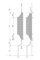
- FIG. 3 is a diagram illustrating an example of a transition sequence between a continuous wave and a pulse wave of RF power according to the embodiment. Note that FIGS. 2 and 3 only show the control conditions for the RF power, and do not show the control conditions for the processing gas, the pressure in the chamber, etc., but from time t 0 to time t in FIGS. 2 and 3 6 and the period after time t6 , plasma processing of the substrate W is performed according to the control conditions set in the recipe used for substrate processing of this embodiment.
- the pulse wave of RF power will also be referred to as "RF pulse”.
- the RF source power is also referred to as “HF” or “HF power”
- the HF pulse wave is also referred to as “HF pulse”.
- the RF bias power is also referred to as “LF” or “LF power”
- the LF pulse wave is also referred to as "LF pulse”.
- 2 and 3 show an example of a supply sequence of HF and LF when performing plasma processing on a substrate, and in each figure, the horizontal axis shows time and the vertical axis shows power (watts). Note that the power values shown in FIGS. 2 and 3 are merely examples, and the power values are not limited thereto. In both FIGS.
- both HF and LF are continuous waves, and each power is continuously supplied to generate plasma of the processing gas.
- both HF and LF supply continuous wave power having a lower power level than the period S1 to continue generating plasma.
- both HF and LF transition from continuous waves to pulse waves.
- both HF and LF supply pulse wave power.
- the HF pulse supplies two levels of power, high and low
- the LF pulse supplies two levels of power, on and off.
- the HF pulse and the LF pulse may be pulse waves with two levels of power, high and low, or two levels of power, on and off.
- the period S32 is a period in which the HF pulse and the LF pulse increase synchronously, and is referred to herein as a "ramp up period.”
- the period S34 is a period in which the HF pulse and the LF pulse decrease synchronously, and is referred to herein as a "ramp down period.”
- the starting points of the period S32 and the period S34 of the HF pulse and the LF pulse may not be completely synchronized but may have a shift (offset).
- the power levels of the HF pulse and the LF pulse increase linearly (linearly), as shown by the dotted line of S32 in FIG.
- the power levels of the HF pulse and the LF pulse increase exponentially, as shown by the dotted line of S32 in FIG. That is, in the HF pulse and LF pulse of the reference example, the power level during the ramp-up period S32 increases monotonically, whereas in the HF pulse and LF pulse of the embodiment, the power level during the ramp-up period S32 initially increases. It increases slowly and then sharply.
- the power levels of the HF pulse and the LF pulse decrease linearly, as shown by the dotted line of S34 in FIG. There is.
- the power levels of the HF pulse and the LF pulse decrease exponentially, as shown by the dotted line of S34 in FIG.
- the power level during the ramp-down period S34 monotonically decreases
- the power level during the ramp-down period S34 initially decreases. It decreases steeply and then gradually.
- the number of times the power levels of the HF pulse and LF pulse are increased and decreased stepwise may be, for example, 10 times, or may be any other number of times.
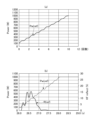
- FIG. 4 is a diagram showing an example of an increasing function of the power level of an RF pulse and a reflected wave in a reference example during the ramp-up period S32.
- FIG. 5 is a diagram showing an example of an increasing function of the power level of the RF pulse and reflected waves in the embodiment during the ramp-up period S32.
- experimental results are shown when HF with a frequency of 40 MHz is used.
- the horizontal axis in FIGS. 4(a), 5(a), and (b) shows the number of times the power level of the RF pulse (HF pulse) is increased stepwise, and the vertical axis shows the power (W).
- the RF power source 31 was controlled so that the HF power monotonically increased during the ramp-up period S32, as shown by Pw(ref) in FIG. 4(a).
- "c” is a parameter that controls the slope (c>0) of the straight line of the HF power Pw(ref) shown in FIG. 4(a), that is, the speed of variation of the power Pw(ref) during the ramp-up period.
- "d” is the HF power level at the start of the ramp-up period, that is, the HF power level when the horizontal axis is 0.
- the number of times on the horizontal axis in FIG. 4(a) is from the start of supply of pulsed HF power (start of the ramp-up period) shown at time t3 in FIG . This is the number of times the HF power level is increased in stages up to the end of the period.
- the HF power Pw (ref) of the reference example is controlled from 100 W set at the supply start time (time t 3 ) to 1000 W at the peak output time (time t 4 ).
- FIG. 4(b) shows a reflected wave R(ref) generated as a result of controlling the HF power Pw(ref) in the reference example shown in FIG. 4(a).
- FIG. 4(b) indicates time, and corresponds to the number of times on the horizontal axis in FIG. 4(a). For example, “0 times" on the horizontal axis in FIG. 4(a) corresponds to “26 seconds” on the horizontal axis in FIG. 4(b), and “10 times” on the horizontal axis in FIG. 4(a) corresponds to "26 seconds” on the horizontal axis in FIG. This corresponds to "28 seconds” on the horizontal axis in (b).
- the vertical axis (right) indicates the HF reflected wave (%), and the vertical axis (left) indicates the HF power (progressive wave power) (W).
- the HF reflected wave (%) is the ratio of the HF reflected wave to the supplied HF traveling wave expressed as a percentage (%).
- the percentage of the HF reflected wave R (ref) was high at about 15% at the beginning of the ramp-up period S32 (26 seconds to 27 seconds), but after 27 seconds, it was almost It became 0%. That is, in the reference example, it was found that HF reflected waves were likely to occur at the beginning of the ramp-up period S32.
- the HF power was controlled using Pw (recipe) in FIG. 5(a) as the target value, and the actual value (not shown) of the HF power during the ramp-up period S32 when three substrates W were actually processed was measured. .
- the coefficient "a” is a parameter that controls the speed of variation of the HF power Pw during the ramp-up period.
- A is the level of RF power at the start of the ramp-up period, and t indicates the time from the start of the ramp-up period.
- the number of times on the horizontal axis in FIGS. 5(a) and (b) is the HF power consumption during the time from the ramp-up start point shown at time t3 in FIG. 3 to the ramp-up end point (peak point) shown at time t4 . This is the number of times to raise the level step by step.
- the HF power Pw of the embodiment is controlled from 100 W set at the supply start time (time t 3 ) to 1000 W set at the peak output time (time t 4 ).
- FIG. 5(c) shows the reflected wave R generated as a result of controlling the HF power Pw in the embodiment shown in FIG. 5(b).
- the vertical axis (right) in FIG. 5(c) indicates the HF reflected wave (%), and the vertical axis (left) indicates the HF power (progressive wave power) (W).
- the HF reflected wave (%) is the ratio of the HF reflected wave to the supplied HF traveling wave expressed as a percentage (%).
- the percentage of the reflected wave R of the HF power is 5% or less, and compared to the reference example of FIG. 4(b), the ramp-up period S32 (26.8 seconds to 28.8 seconds
- the reflected waves decreased over the entire period (seconds). That is, in the embodiment, it has been found that HF reflected waves are unlikely to occur during the ramp-up period S32. In other words, in the reference example, a large reflected wave is generated in the first half of the ramp-up period S32 when the HF power is low, and in the embodiment, a small reflected wave is generated throughout the ramp-up period S32.
- the maximum value of the reflected wave is reduced to 5% or less of the HF traveling wave, and plasma load fluctuation is reduced.
- HF power is simply increased in the ramp-up period S32, reflected waves are likely to occur when the power is low (see FIG. 4(b)). For example, this is because the plasma tends to become unstable when the HF power is low (for example, 400 W or less).
- the HF power is low (for example, 400 W or less) at which the plasma tends to become unstable, the HF power The speed of fluctuation can be slowed down.
- the impedance matching accuracy between the RF power source 31 and the load is improved, thereby suppressing reflected waves of the HF power, Plasma load fluctuations can be suppressed.
- the HF pulse was exponentially increased as an example of the RF power in the ramp-up period S32, but the same effect can be obtained by controlling the LF power in the same way. That is, by increasing the LF pulse exponentially in the ramp-up period S32, reflected waves can be reduced, and plasma load fluctuations can be suppressed.
- the RF power is not limited to being increased exponentially in the ramp-up period S32.
- the RF power source 31 may be controlled so that the increasing function of the power level from the start of supply of RF pulses to the peak point becomes a downwardly convex function.
- the speed of fluctuation of the RF power can be slowed down, the reflected waves of the RF power can be suppressed, and the load fluctuation of the plasma can be suppressed.
- controlling the RF power so that the increasing function becomes a downwardly convex function means that when the horizontal axis is time and the vertical axis is RF power, the power when the RF pulse is on or high is downward. It becomes convex and increases the RF power over time.
- the increasing function of the power level from the start point of RF power supply (for example, time t 3 in FIG. 3 ) to the peak point (for example, time t 4 in FIG. 3) is expressed by the following equations (1) and (2).
- the RF power supply 31 is controlled so as to satisfy the function shown in (). The explanation will be divided into cases (i) and (ii).
- the RF power source 31 may be controlled so that only the HF power during the ramp-up period S32 becomes a downwardly convex function. In this case, the LF power during the ramp-up period S32 may increase monotonically. Further, the RF power source 31 may be controlled so that only the LF power during the ramp-up period S32 becomes a downwardly convex function. In this case, the HF power during the ramp-up period S32 may increase monotonically. Further, the RF power source 31 may be controlled so that both the HF power and the LF power in the ramp-up period S32 have a downwardly convex function.
- FIG. 6 is a diagram showing an example of a reduction function of the power level of the RF pulse and reflected waves in the embodiment during the ramp-down period S34.
- experimental results are shown when HF with a frequency of 40 MHz is used.
- the control device 2 adjusts the HF power so that it follows the curve set in the recipe during the ramp-down period S34, as shown in Pw (recipe) in FIG. 6(a).
- the RF power source 31 was controlled so that the HF power decreased exponentially.
- the HF power was controlled using Pw (recipe) in FIG. 6(a) as the target value, and the actual value (not shown) of the HF power during the ramp-down period S34 when three substrates W were actually processed was measured. .
- the coefficient "b" is a parameter that controls the speed of variation of the HF power Pw during the ramp-down period.
- “B” is the level of RF power at the beginning of the ramp-down period, and t indicates the time from the beginning of the ramp-down period.
- the number of times on the horizontal axis in FIGS. 6(a) and (b) is from the peak end point (rampdown start point) shown at time t5 in FIG. 3 to the supply end point (rampdown end point) shown at time t6 in FIG. This is the number of times the HF power level is gradually lowered over time.
- the HF power Pw of the embodiment is controlled from 1000 W set at the peak end time (time t 5 ) to 100 W at the supply end time (time t 6 ).
- FIG. 6(c) shows the reflected wave R generated as a result of controlling the HF power Pw in the embodiment shown in FIG. 6(b).
- FIG. 6(c) indicates time, and corresponds to the number of times on the horizontal axis in FIG. 6(b).
- the vertical axis (right) indicates the HF reflected wave (%)
- the vertical axis (left) indicates the HF power (progressive wave power) (W).
- the HF reflected wave (%) is the ratio of the HF reflected wave to the supplied HF traveling wave expressed as a percentage (%).
- the percentage R of reflected waves of HF power is 17.5% or less, and there are few reflected waves throughout the ramp-down period S34.
- the maximum value of the reflected wave is reduced to 17.5% or less of the HF traveling wave in the ramp-down period S34, and the plasma load fluctuation is reduced.
- HF power is simply decreased in the ramp-down period S34, reflected waves are likely to occur when the power is low. For example, this is because the plasma tends to become unstable when the HF power is low (for example, 400 W or less).
- the HF power is low (for example, 400 W or less) at which the plasma tends to become unstable
- the HF power The speed of fluctuation can be slowed down.
- the impedance matching accuracy between the RF power source 31 and the load is improved, thereby suppressing reflected waves of the HF power, Plasma load fluctuations can be suppressed.
- the HF power is exponentially reduced as an example of RF power in the ramp-down period S34, but the same effect can be obtained by controlling the LF power in the same manner. That is, by exponentially decreasing the LF pulse during the ramp-down period S34, reflected waves can be reduced, and plasma load fluctuations can be suppressed.
- the RF power is not limited to decreasing exponentially in the ramp-down period S34.
- the RF power source 31 may be controlled so that the decreasing function of the power level from the end of the peak of the RF pulse to the end of supply becomes a downwardly convex function. Thereby, reflected waves of RF power can be suppressed, and plasma load fluctuations can be suppressed.
- controlling the RF power so that the decreasing function becomes a downwardly convex function means that when the horizontal axis is time and the vertical axis is RF power, the power when the RF pulse is on or high is downward. It is to become convex and reduce RF power over time.
- the power level decreasing function from the end of the peak of RF power (for example, time t 5 in FIG. 3) to the end of supply (for example, time t 6 in FIG. 3) is expressed by the following equations (3) and (4).
- the RF power supply 31 is controlled so as to satisfy the function shown in ().
- B indicates the RF power level at the end of the peak of RF power.
- t indicates the time from the end of the peak of RF power.
- Pw(t) indicates the RF power level at time t from the peak end point.
- P min indicates the minimum value of the RF power level.
- t max indicates the time from the end of the peak of RF power to the end of supply.
- the RF power source 31 may be controlled so that only the HF power in the ramp-down period S34 becomes a downwardly convex function.
- the LF power during the ramp-down period S34 may monotonically decrease.
- the RF power source 31 may be controlled so that only the LF power during the ramp-down period S34 becomes a downwardly convex function.
- the HF power during the ramp-down period S34 may monotonically decrease.
- the RF power source 31 may be controlled so that both the HF power and the LF power in the ramp-down period S34 become a downwardly convex function.
- FIG. 1 Another example in which the power level increasing function from the start of supply of pulsed RF power to the peak point is a downwardly convex function may include a case where the slope of the convex function changes midway. For example, from the start of RF power supply (for example, time t 3 in FIG. 3 ) to a time (time tt) halfway between the peak point (for example, time t 4 in FIG. 3), there is a gentle slope (slope a1). ) is the straight line. From time tt to the peak point (for example, time t 4 in FIG. 3), a straight line may be formed with a slope a2 different from the slope a1, and the slope may be changed.
- the slope a1 is set to a smaller value than the slope a2, making it a downwardly convex function.
- the slope a1 is set to a smaller value than the slope a2, making it a downwardly convex function.
- the slope is controlled by controlling the slope to a downwardly convex increasing function with a gentle slope for a predetermined period of time (until time tt) from the start of RF power supply, reflected waves of RF power are suppressed and the ramp-up period is controlled. Plasma load fluctuations can be suppressed.
- the straight line from the start point of RF power supply to the peak point point is described as a combination of straight lines whose slope changes at time tt, but the present invention is not limited to this.
- FIG. 2 Another example in which the decreasing function of the power level from the peak end point of pulsed RF power (ramp down start point) to the supply end point (ramp down end point) is a downwardly convex function. It may also include a case where the slope changes.
- a straight line with an inclination a3 is defined from the end of the peak of RF power (for example, time t 5 in FIG. 3) to a time (time tk) halfway between the end of supply (for example, time t 6 in FIG. 3). From time tk to the end of supply (for example, time t 6 in FIG. 3), the straight line may have a slope a4 different from a3, and the slope may be changed.
- the slope a4 is set to a smaller value than the slope a3, making it a downwardly convex function.
- the straight line from the end of the peak of RF power to the end of supply is described as a combination of straight lines whose slope changes at time tk, but the present invention is not limited to this. It is not limited to a straight line, but may be a combination of a straight line and/or a curved line, as long as the slope can be made gentle for a while before the RF power supply ends and controlled to a downwardly convex decreasing function.
- plasma load fluctuations can be suppressed.
- FIG. 7 is a flowchart illustrating an example of the plasma processing method according to the embodiment.
- the power supply system includes an RF power supply 31 that supplies pulsed RF power to the plasma processing chamber 10 and/or the substrate support 11, and a control device 2 that controls the supply of the pulsed RF power.
- the RF power described below may be HF power, LF power, HF power and LF power.
- step ST1 the control device 2 prepares a substrate on the substrate support section 11, supplies a processing gas from the gas supply section 20 into the plasma processing chamber 10, and uses continuous wave RF from the RF power source 31. Control to supply power. As a result, the processing gas is turned into plasma, and the substrate is subjected to plasma processing.
- step ST2 the control device 2 determines whether to shift the RF power from continuous waves to pulse waves. If the control device 2 determines that the RF power is not to be shifted from a continuous wave to a pulse wave (NO in step ST2), it repeats the determination process in step ST2 until it determines YES in step ST2.
- control device 2 determines that the RF power is to be shifted from a continuous wave to a pulse wave
- the control device 2 proceeds to step ST3, and controls the control device 2 so that the increasing function of the RF power from the start of supply of RF pulses to the point of peak occurrence becomes a downwardly convex function.
- the RF power supply 31 is controlled to proceed to step ST4.
- step ST4 the control device 2 determines whether the RF power shifts from a pulse wave to a continuous wave. If the control device 2 determines that the RF power does not shift from a pulse wave to a continuous wave (NO in step ST4), it repeats the determination process in step ST4 until it determines YES in step ST4.
- control device 2 determines that the RF power shifts from a pulse wave to a continuous wave
- the control device 2 proceeds to step ST5, and the decreasing function of the RF power level from the end of the peak of the RF pulse to the end of supply becomes a downwardly convex function.
- the RF power supply 31 is controlled as shown in FIG. 2, and the process proceeds to the next step.
- reflected waves of RF power can be suppressed, and plasma load fluctuations during the ramp-up period and/or the ramp-down period can be suppressed.
- the plasma processing apparatus, power supply system, and plasma processing method according to the embodiments disclosed herein are illustrative in all respects and should not be considered restrictive.
- the embodiments can be modified and improved in various ways without departing from the scope and spirit of the appended claims.
- the matters described in the plurality of embodiments described above may be configured in other ways without being inconsistent, and may be combined without being inconsistent.
- the plasma processing apparatus of the present disclosure includes an Atomic Layer Deposition (ALD) apparatus, Capacitively Coupled Plasma (CCP), Inductively Coupled Plasma (ICP), Radial Line Slot Antenna (RLSA), Electron Cyclotron Resonance Plasma (ECR), Helicon Wave Plasma ( Applicable to any type of device (HWP).
- ALD Atomic Layer Deposition
- CCP Capacitively Coupled Plasma
- ICP Inductively Coupled Plasma
- RLSA Radial Line Slot Antenna
- ECR Electron Cyclotron Resonance Plasma
- HWP Helicon Wave Plasma
- Plasma processing apparatus 2 Control device 2a Computer 2a1 Processing section 2a2 Storage section 2a3 Communication interface 10 Plasma processing chamber 11 Substrate support section 13 Shower head 21 Gas source 20 Gas supply section 30 Power supply 31 RF power supply 31a First RF generation section 31b No. 2 RF generation section 32a First DC generation section 32b Second DC generation section 40 Exhaust system 111 Main body section 112 Ring assembly
Landscapes
- Chemical & Material Sciences (AREA)
- Engineering & Computer Science (AREA)
- Physics & Mathematics (AREA)
- Plasma & Fusion (AREA)
- Analytical Chemistry (AREA)
- Mechanical Engineering (AREA)
- Chemical Kinetics & Catalysis (AREA)
- Materials Engineering (AREA)
- General Chemical & Material Sciences (AREA)
- Metallurgy (AREA)
- Organic Chemistry (AREA)
- Electromagnetism (AREA)
- Spectroscopy & Molecular Physics (AREA)
- Drying Of Semiconductors (AREA)
- Plasma Technology (AREA)
- Chemical Vapour Deposition (AREA)
Priority Applications (4)
| Application Number | Priority Date | Filing Date | Title |
|---|---|---|---|
| JP2024517195A JPWO2023210399A1 (enExample) | 2022-04-25 | 2023-04-13 | |
| CN202380034853.4A CN119054418A (zh) | 2022-04-25 | 2023-04-13 | 等离子体处理装置、电源系统和等离子体处理方法 |
| KR1020247038364A KR20250003883A (ko) | 2022-04-25 | 2023-04-13 | 플라즈마 처리 장치, 전원 시스템 및 플라즈마 처리 방법 |
| US18/788,228 US20240387143A1 (en) | 2022-04-25 | 2024-07-30 | Plasma processing apparatus, power source system, and plasma processing method |
Applications Claiming Priority (2)
| Application Number | Priority Date | Filing Date | Title |
|---|---|---|---|
| JP2022071371 | 2022-04-25 | ||
| JP2022-071371 | 2022-04-25 |
Related Child Applications (1)
| Application Number | Title | Priority Date | Filing Date |
|---|---|---|---|
| US18/788,228 Continuation US20240387143A1 (en) | 2022-04-25 | 2024-07-30 | Plasma processing apparatus, power source system, and plasma processing method |
Publications (1)
| Publication Number | Publication Date |
|---|---|
| WO2023210399A1 true WO2023210399A1 (ja) | 2023-11-02 |
Family
ID=88518519
Family Applications (1)
| Application Number | Title | Priority Date | Filing Date |
|---|---|---|---|
| PCT/JP2023/015084 Ceased WO2023210399A1 (ja) | 2022-04-25 | 2023-04-13 | プラズマ処理装置、電源システム及びプラズマ処理方法 |
Country Status (6)
| Country | Link |
|---|---|
| US (1) | US20240387143A1 (enExample) |
| JP (1) | JPWO2023210399A1 (enExample) |
| KR (1) | KR20250003883A (enExample) |
| CN (1) | CN119054418A (enExample) |
| TW (1) | TW202410119A (enExample) |
| WO (1) | WO2023210399A1 (enExample) |
Cited By (1)
| Publication number | Priority date | Publication date | Assignee | Title |
|---|---|---|---|---|
| WO2026034233A1 (ja) * | 2024-08-08 | 2026-02-12 | 東京エレクトロン株式会社 | プラズマ処理装置及び電源システム |
Citations (8)
| Publication number | Priority date | Publication date | Assignee | Title |
|---|---|---|---|---|
| JP2009033080A (ja) * | 2006-10-06 | 2009-02-12 | Tokyo Electron Ltd | プラズマエッチング装置、プラズマエッチング方法およびコンピュータ読取可能な記憶媒体 |
| JP2013122966A (ja) * | 2011-12-09 | 2013-06-20 | Tokyo Electron Ltd | プラズマ処理方法及びプラズマ処理装置 |
| JP2014002898A (ja) * | 2012-06-18 | 2014-01-09 | Kyosan Electric Mfg Co Ltd | 高周波電力供給装置、及び反射波電力制御方法 |
| JP2015095493A (ja) * | 2013-11-08 | 2015-05-18 | 株式会社日立ハイテクノロジーズ | プラズマ処理方法 |
| US20170053811A1 (en) * | 2015-08-21 | 2017-02-23 | Lam Research Corporation | Pulsing rf power in etch process to enhance tungsten gapfill performance |
| US20170069493A1 (en) * | 2015-09-04 | 2017-03-09 | Applied Materials, Inc. | Methods and apparatus for uniformly and high-rate depositing low resistivity microcrystalline silicon films for display devices |
| US20170330764A1 (en) * | 2016-05-12 | 2017-11-16 | Lam Research Corporation | Methods and apparatuses for controlling transitions between continuous wave and pulsing plasmas |
| WO2020223129A1 (en) * | 2019-04-29 | 2020-11-05 | Lam Research Corporation | Systems and methods for multi-level pulsing in rf plasma tools |
Family Cites Families (3)
| Publication number | Priority date | Publication date | Assignee | Title |
|---|---|---|---|---|
| JP7175239B2 (ja) * | 2018-06-22 | 2022-11-18 | 東京エレクトロン株式会社 | 制御方法、プラズマ処理装置、プログラム及び記憶媒体 |
| US12046450B2 (en) * | 2020-09-29 | 2024-07-23 | Lam Research Corporation | Synchronization of RF generators |
| US11694876B2 (en) * | 2021-12-08 | 2023-07-04 | Applied Materials, Inc. | Apparatus and method for delivering a plurality of waveform signals during plasma processing |
-
2023
- 2023-04-13 JP JP2024517195A patent/JPWO2023210399A1/ja active Pending
- 2023-04-13 CN CN202380034853.4A patent/CN119054418A/zh active Pending
- 2023-04-13 KR KR1020247038364A patent/KR20250003883A/ko active Pending
- 2023-04-13 TW TW112113744A patent/TW202410119A/zh unknown
- 2023-04-13 WO PCT/JP2023/015084 patent/WO2023210399A1/ja not_active Ceased
-
2024
- 2024-07-30 US US18/788,228 patent/US20240387143A1/en active Pending
Patent Citations (8)
| Publication number | Priority date | Publication date | Assignee | Title |
|---|---|---|---|---|
| JP2009033080A (ja) * | 2006-10-06 | 2009-02-12 | Tokyo Electron Ltd | プラズマエッチング装置、プラズマエッチング方法およびコンピュータ読取可能な記憶媒体 |
| JP2013122966A (ja) * | 2011-12-09 | 2013-06-20 | Tokyo Electron Ltd | プラズマ処理方法及びプラズマ処理装置 |
| JP2014002898A (ja) * | 2012-06-18 | 2014-01-09 | Kyosan Electric Mfg Co Ltd | 高周波電力供給装置、及び反射波電力制御方法 |
| JP2015095493A (ja) * | 2013-11-08 | 2015-05-18 | 株式会社日立ハイテクノロジーズ | プラズマ処理方法 |
| US20170053811A1 (en) * | 2015-08-21 | 2017-02-23 | Lam Research Corporation | Pulsing rf power in etch process to enhance tungsten gapfill performance |
| US20170069493A1 (en) * | 2015-09-04 | 2017-03-09 | Applied Materials, Inc. | Methods and apparatus for uniformly and high-rate depositing low resistivity microcrystalline silicon films for display devices |
| US20170330764A1 (en) * | 2016-05-12 | 2017-11-16 | Lam Research Corporation | Methods and apparatuses for controlling transitions between continuous wave and pulsing plasmas |
| WO2020223129A1 (en) * | 2019-04-29 | 2020-11-05 | Lam Research Corporation | Systems and methods for multi-level pulsing in rf plasma tools |
Cited By (1)
| Publication number | Priority date | Publication date | Assignee | Title |
|---|---|---|---|---|
| WO2026034233A1 (ja) * | 2024-08-08 | 2026-02-12 | 東京エレクトロン株式会社 | プラズマ処理装置及び電源システム |
Also Published As
| Publication number | Publication date |
|---|---|
| CN119054418A (zh) | 2024-11-29 |
| KR20250003883A (ko) | 2025-01-07 |
| TW202410119A (zh) | 2024-03-01 |
| JPWO2023210399A1 (enExample) | 2023-11-02 |
| US20240387143A1 (en) | 2024-11-21 |
Similar Documents
| Publication | Publication Date | Title |
|---|---|---|
| TW202147925A (zh) | 電漿處理裝置及電漿處理方法 | |
| TWI905447B (zh) | 電漿處理裝置及電漿處理方法 | |
| CN118414889A (zh) | 等离子体处理装置、电源系统、控制方法、程序和存储介质 | |
| JP7537845B2 (ja) | プラズマ処理装置 | |
| JP7638371B2 (ja) | プラズマ処理装置及びrfシステム | |
| US20240387143A1 (en) | Plasma processing apparatus, power source system, and plasma processing method | |
| JP7632967B2 (ja) | プラズマ処理装置及びプラズマ処理方法 | |
| WO2022215556A1 (ja) | エッチング方法及びエッチング処理装置 | |
| US12142465B2 (en) | Plasma processing method and plasma processing apparatus | |
| WO2023204101A1 (ja) | プラズマ処理装置及びプラズマ処理方法 | |
| WO2022124334A1 (ja) | プラズマ処理方法及びプラズマ処理装置 | |
| TW202245053A (zh) | 蝕刻方法及蝕刻處理裝置 | |
| KR102958019B1 (ko) | 플라즈마 처리 방법 및 플라즈마 처리 장치 | |
| US20230086580A1 (en) | Etching method and plasma processing apparatus | |
| JP7537844B2 (ja) | プラズマ処理装置 | |
| JP7597463B2 (ja) | プラズマ処理装置及びプラズマ処理方法 | |
| US20240105424A1 (en) | Plasma processing apparatus and plasma processing method | |
| KR20260041165A (ko) | 플라즈마 처리 장치 및 에칭 방법 | |
| WO2024070580A1 (ja) | プラズマ処理装置及び電源システム | |
| JP2024135093A (ja) | プラズマ処理装置 | |
| WO2023189292A1 (ja) | プラズマ処理装置 | |
| KR20250165342A (ko) | 에칭 장치 및 에칭 방법 | |
| WO2024070578A1 (ja) | プラズマ処理装置及び電源システム | |
| TW202439443A (zh) | 蝕刻方法及電漿處理裝置 |
Legal Events
| Date | Code | Title | Description |
|---|---|---|---|
| 121 | Ep: the epo has been informed by wipo that ep was designated in this application |
Ref document number: 23796143 Country of ref document: EP Kind code of ref document: A1 |
|
| WWE | Wipo information: entry into national phase |
Ref document number: 2024517195 Country of ref document: JP |
|
| WWE | Wipo information: entry into national phase |
Ref document number: 202380034853.4 Country of ref document: CN |
|
| ENP | Entry into the national phase |
Ref document number: 20247038364 Country of ref document: KR Kind code of ref document: A |
|
| WWE | Wipo information: entry into national phase |
Ref document number: 1020247038364 Country of ref document: KR |
|
| NENP | Non-entry into the national phase |
Ref country code: DE |
|
| 122 | Ep: pct application non-entry in european phase |
Ref document number: 23796143 Country of ref document: EP Kind code of ref document: A1 |