WO2023210118A1 - Module d'antenne - Google Patents
Module d'antenne Download PDFInfo
- Publication number
- WO2023210118A1 WO2023210118A1 PCT/JP2023/005375 JP2023005375W WO2023210118A1 WO 2023210118 A1 WO2023210118 A1 WO 2023210118A1 JP 2023005375 W JP2023005375 W JP 2023005375W WO 2023210118 A1 WO2023210118 A1 WO 2023210118A1
- Authority
- WO
- WIPO (PCT)
- Prior art keywords
- substrate
- radiating element
- antenna module
- module according
- antenna
- Prior art date
Links
- 239000000758 substrate Substances 0.000 claims abstract description 174
- 230000010287 polarization Effects 0.000 claims description 9
- 230000005855 radiation Effects 0.000 description 110
- 238000004891 communication Methods 0.000 description 12
- 101100489717 Saccharomyces cerevisiae (strain ATCC 204508 / S288c) GND2 gene Proteins 0.000 description 10
- 238000010586 diagram Methods 0.000 description 10
- 239000011347 resin Substances 0.000 description 9
- 229920005989 resin Polymers 0.000 description 9
- 101100489713 Saccharomyces cerevisiae (strain ATCC 204508 / S288c) GND1 gene Proteins 0.000 description 7
- 239000010410 layer Substances 0.000 description 7
- 230000004048 modification Effects 0.000 description 6
- 238000012986 modification Methods 0.000 description 6
- 238000010030 laminating Methods 0.000 description 4
- 229920000106 Liquid crystal polymer Polymers 0.000 description 2
- 239000004977 Liquid-crystal polymers (LCPs) Substances 0.000 description 2
- 239000000919 ceramic Substances 0.000 description 2
- 230000008878 coupling Effects 0.000 description 2
- 238000010168 coupling process Methods 0.000 description 2
- 238000005859 coupling reaction Methods 0.000 description 2
- 230000009977 dual effect Effects 0.000 description 2
- 230000000694 effects Effects 0.000 description 2
- 238000000034 method Methods 0.000 description 2
- 229920000139 polyethylene terephthalate Polymers 0.000 description 2
- 239000005020 polyethylene terephthalate Substances 0.000 description 2
- 239000004593 Epoxy Substances 0.000 description 1
- -1 Polyethylene Terephthalate Polymers 0.000 description 1
- 239000004642 Polyimide Substances 0.000 description 1
- 230000005540 biological transmission Effects 0.000 description 1
- 230000015572 biosynthetic process Effects 0.000 description 1
- 230000001186 cumulative effect Effects 0.000 description 1
- 230000007423 decrease Effects 0.000 description 1
- 230000006866 deterioration Effects 0.000 description 1
- 238000005315 distribution function Methods 0.000 description 1
- 239000000463 material Substances 0.000 description 1
- 239000002184 metal Substances 0.000 description 1
- 230000010363 phase shift Effects 0.000 description 1
- 229920001721 polyimide Polymers 0.000 description 1
- 239000002356 single layer Substances 0.000 description 1
- 229910000679 solder Inorganic materials 0.000 description 1
- 238000003786 synthesis reaction Methods 0.000 description 1
Images


Classifications
-
- H—ELECTRICITY
- H01—ELECTRIC ELEMENTS
- H01Q—ANTENNAS, i.e. RADIO AERIALS
- H01Q1/00—Details of, or arrangements associated with, antennas
- H01Q1/52—Means for reducing coupling between antennas; Means for reducing coupling between an antenna and another structure
-
- H—ELECTRICITY
- H01—ELECTRIC ELEMENTS
- H01Q—ANTENNAS, i.e. RADIO AERIALS
- H01Q13/00—Waveguide horns or mouths; Slot antennas; Leaky-waveguide antennas; Equivalent structures causing radiation along the transmission path of a guided wave
- H01Q13/08—Radiating ends of two-conductor microwave transmission lines, e.g. of coaxial lines, of microstrip lines
-
- H—ELECTRICITY
- H01—ELECTRIC ELEMENTS
- H01Q—ANTENNAS, i.e. RADIO AERIALS
- H01Q21/00—Antenna arrays or systems
- H01Q21/24—Combinations of antenna units polarised in different directions for transmitting or receiving circularly and elliptically polarised waves or waves linearly polarised in any direction
-
- H—ELECTRICITY
- H01—ELECTRIC ELEMENTS
- H01Q—ANTENNAS, i.e. RADIO AERIALS
- H01Q21/00—Antenna arrays or systems
- H01Q21/28—Combinations of substantially independent non-interacting antenna units or systems
-
- H—ELECTRICITY
- H01—ELECTRIC ELEMENTS
- H01Q—ANTENNAS, i.e. RADIO AERIALS
- H01Q21/00—Antenna arrays or systems
- H01Q21/30—Combinations of separate antenna units operating in different wavebands and connected to a common feeder system
-
- H—ELECTRICITY
- H01—ELECTRIC ELEMENTS
- H01Q—ANTENNAS, i.e. RADIO AERIALS
- H01Q23/00—Antennas with active circuits or circuit elements integrated within them or attached to them
Definitions
- the present disclosure relates to an antenna module, and more specifically, to a technique for downsizing an antenna module that can radiate radio waves in two directions.
- Patent Document 1 discloses an antenna module having a bent dielectric substrate, in which radiating elements are arranged on two surfaces with different normal directions. .
- Patent Document 1 The antenna module disclosed in US Pat. No. 1,110,8157 (Patent Document 1) may be used, for example, in a communication device typified by a mobile terminal such as a mobile phone or a smartphone. It is desired that such communication devices be further miniaturized and thinner, and along with this, the antenna modules installed in such communication devices are also required to be further miniaturized and lower in profile. .
- the present disclosure has been made in order to solve the above-mentioned problems, and the purpose is to achieve a reduction in height while ensuring mechanical strength in an antenna module that can radiate radio waves in two directions. That's true.
- the antenna module includes a first substrate on which a flat plate-shaped first radiating element is arranged, and a second substrate on which a flat plate-shaped second radiating element is arranged.
- the first substrate has a first surface and a second surface facing each other.
- the first radiating element is disposed on the second surface of the first substrate or at a position between the first surface and the second surface.
- a recessed portion recessed in the normal direction of the first surface is formed on the first surface of the first substrate.
- the second substrate includes a first region arranged to fit inside the recess and a second region in contact with the first surface of the first substrate.
- the normal direction of the second radiating element is different from the normal direction of the first radiating element.
- the second substrate on which the second radiating element having a different radiation direction (normal direction) is disposed is fitted into the recess formed in the first substrate on which the first radiating element is disposed.
- the second substrate is fixed on the main surface (first surface) of the first substrate.
- FIG. 1 is a block diagram of a communication device to which the antenna module according to Embodiment 1 is applied.
- FIG. FIG. 2 is a perspective view of the antenna module of FIG. 1;
- FIG. 2 is a side perspective view of the antenna module of FIG. 1;
- FIG. 3 is a diagram for explaining an antenna block. It is a figure for explaining the antenna block of a modification.
- FIG. 3 is a side perspective view of an antenna module according to a second embodiment.
- FIG. 3 is a diagram for explaining antenna characteristics of a radiating element on the main board side in the antenna modules of Embodiment 1 and Embodiment 2;
- FIG. 7 is a side perspective view of an antenna module according to Embodiment 3;
- FIG. 7 is a diagram for explaining antenna characteristics of a radiating element on the antenna block side in the antenna modules of Embodiment 2 and Embodiment 3;
- FIG. 7 is a side perspective view of an antenna module according to Embodiment 4.
- FIG. 7 is a perspective view of an antenna module according to a fifth embodiment. It is a perspective view of the antenna module of a modification.
- FIG. 1 is a block diagram of a communication device 10 to which an antenna module 100 according to the present embodiment is applied.
- the communication device 10 is, for example, a mobile terminal such as a mobile phone, a smartphone, or a tablet, or a personal computer with a communication function.
- An example of the frequency band of radio waves used in the antenna module 100 according to the present embodiment is, for example, radio waves in the millimeter wave band with center frequencies of 28 GHz, 39 GHz, and 60 GHz, but radio waves in frequency bands other than the above may also be used. Applicable.
- communication device 10 includes an antenna module 100 and a BBIC 200 that constitutes a baseband signal processing circuit.
- the antenna module 100 includes an RFIC 110, which is an example of a power feeding device, and an antenna device 120.
- the communication device 10 up-converts the signal transmitted from the BBIC 200 to the antenna module 100 into a high-frequency signal and radiates it from the antenna device 120, and down-converts the high-frequency signal received by the antenna device 120 and processes the signal in the BBIC 200. do.
- the antenna device 120 includes a dielectric substrate 130A and a plurality of dielectric substrates 130B.
- a plurality of radiating elements 125A are arranged on the dielectric substrate 130A.
- Each radiation element 125A includes a radiation electrode 121A and a radiation electrode 122A having a flat plate shape.
- a radiating element 125B is arranged on each dielectric substrate 130B.
- the radiation element 125B includes a radiation electrode 121B and a radiation electrode 122B each having a flat plate shape.
- Each radiation electrode included in the radiation elements 125A and 125B is a flat patch antenna having a circular, elliptical, or polygonal shape.
- each radiation electrode is a microstrip antenna having a substantially square shape.
- the size of the radiation electrode 121A is smaller than the size of the radiation electrode 122A. Therefore, the frequency band of the radio waves radiated from the radiation electrode 121A is higher than the frequency band of the radio waves radiated from the radiation electrode 122A.
- the size of the radiation electrode 121B is smaller than the size of the radiation electrode 122B, and the frequency band of the radio waves radiated from the radiation electrode 121B is higher than the frequency band of the radio waves radiated from the radiation electrode 122B.
- the antenna module 100 in the example of FIG. 1 is a so-called dual-band type antenna module that can radiate radio waves in two different frequency bands from each of the two dielectric substrates 130A and 130B.
- the dielectric substrate 130A on which the plurality of radiating elements 125A are arranged is also referred to as the "main board 108", and the configuration of each dielectric substrate 130B on which the radiating elements 125B are arranged is referred to as the "antenna block 107". ” is also called.
- the antenna device 120 has a configuration in which a plurality of antenna blocks 107 are attached to the main board 108.
- FIG. 1 an example of a configuration is shown in which the antenna device 120 includes four dielectric substrates 130B, and four radiating elements 125A are arranged on the dielectric substrate 130A.
- the number of elements 125A is not limited to this.
- FIG. 1 shows an example in which the radiating elements 125A are arranged in a one-dimensional array on the dielectric substrate 130A, two radiating elements 125A are arranged on the dielectric substrate 130A. They may be arranged in a dimensional array. Alternatively, a configuration may be adopted in which a single radiating element 125A is disposed on the dielectric substrate 130A.
- the RFIC 110 includes four power supply circuits 110A to 110D.
- the power supply circuit 110A is a circuit for supplying a high frequency signal to the radiation electrode 121A on the main board 108 side.
- the power supply circuit 110B is a circuit for supplying a high frequency signal to the radiation electrode 122A on the main board 108 side.
- the feed circuit 110C is a circuit for supplying a high frequency signal to the radiation electrode 122B on the antenna block 107 side.
- the feeding circuit 110D is a circuit for supplying a high frequency signal to the radiation electrode 121B on the antenna block 107 side. Note that since the internal configuration of the power supply circuits 110A to 110D is common, in order to simplify the explanation, in FIG. Omitted. Below, the function of the power supply circuit 110A will be explained as a representative.
- the power supply circuit 110A includes switches 111A to 111D, 113A to 113D, 117, power amplifiers 112AT to 112DT, low noise amplifiers 112AR to 112DR, attenuators 114A to 114D, phase shifters 115A to 115D, and signal synthesis/distribution. 116, a mixer 118, and an amplifier circuit 119.
- the switches 111A to 111D and 113A to 113D are switched to the power amplifiers 112AT to 112DT, and the switch 117 is connected to the transmitting side amplifier of the amplifier circuit 119.
- the switches 111A to 111D and 113A to 113D are switched to the low noise amplifiers 112AR to 112DR, and the switch 117 is connected to the receiving amplifier of the amplifier circuit 119.
- the intermediate frequency signal transmitted from the BBIC 200 is amplified by the amplifier circuit 119 and up-converted by the mixer 118.
- the transmission signal which is an up-converted high-frequency signal, is divided into four waves by the signal combiner/distributor 116, passes through corresponding signal paths, and is fed to different radiation electrodes 121A.
- the degree of phase shift of the phase shifters 115A to 115D arranged in each signal path By individually adjusting the degree of phase shift of the phase shifters 115A to 115D arranged in each signal path, the directivity of the radio waves output from the radiation electrode 121A can be adjusted.
- the received signal which is a high-frequency signal received by each radiation electrode 121A, is transmitted to the power supply circuit 110A of the RFIC 110, and multiplexed in the signal combiner/distributor 116 via four different signal paths.
- the multiplexed received signal is down-converted by mixer 118, further amplified by amplifier circuit 119, and transmitted to BBIC 200.
- the RFIC 110 is formed, for example, as a one-chip integrated circuit component including the circuit configuration described above.
- each feed circuit may be formed as a separate integrated circuit component.
- the equipment (switch, power amplifier, low noise amplifier, attenuator, phase shifter) corresponding to each radiating element may be formed as a one-chip integrated circuit component for each corresponding radiating element.
- FIG. 2 is a perspective view of the antenna module 100 according to the first embodiment.
- the upper part (A) shows a state in which the main board 108 and the antenna block 107 are separated.
- the lower part (B) of FIG. 2 shows a state in which the antenna block 107 is attached to the main board 108.
- FIG. 3 is a side perspective view of the antenna module 100 viewed from the positive direction of the X-axis in the state shown in FIG. 2(B).
- FIG. 4 is a perspective view of the antenna block 107 alone.
- FIG. 4 is a perspective view of the antenna block 107 when the plane in the Y-axis direction is the front. Further, the lower part (B) of FIG. 4 is a perspective view of the antenna block 107 when the surface in the Z-axis direction is the front.
- the radiation element 125A has a single radiation electrode 121A
- the radiation element 125B has a single radiation electrode 121B.
- five radiating elements are arranged on the dielectric substrate 130A, and five antenna blocks 107 are provided correspondingly.
- the antenna module 100 includes, in addition to dielectric substrates 130A, 130B, radiation electrodes 121A, 121B, and RFIC 110, power supply wiring 141A, 141B, connection electrodes 151, 152, and ground electrode GND1, Further includes GND2.
- the normal direction of the main surface of the dielectric substrate 130A will be referred to as the Z-axis direction.
- the arrangement direction of the radiation electrode 121A and the antenna block 107 is defined as the X axis, and the direction orthogonal to the X axis is defined as the Y axis.
- the radiation direction of the radio waves from the radiation electrode 121A is the positive direction of the Z-axis
- the radiation direction of the radio waves from the radiation electrode 121B is the positive direction of the Y-axis. That is, the normal direction of the radiation electrode 121A and the normal direction of the radiation electrode 121B are orthogonal.
- the dielectric substrates 130A and 130B are, for example, low temperature co-fired ceramics (LTCC) multilayer substrates, multilayer resin substrates formed by laminating a plurality of resin layers made of resin such as epoxy or polyimide. , a multilayer resin substrate formed by laminating multiple resin layers made of liquid crystal polymer (LCP) with a lower dielectric constant, and a multilayer resin substrate formed by laminating multiple resin layers made of fluororesin.
- LCP liquid crystal polymer
- the dielectric substrate 130A of the main substrate 108 has a substantially rectangular shape with the long side in the X-axis direction when viewed from the Z-axis direction.
- a plurality of recesses (notches) 170 are formed on one long side of the dielectric substrate 130A along the X-axis (the end in the positive direction of the Y-axis).
- the recess 170 is formed up to the side surface (end) of the dielectric substrate 130A in the positive direction of the Y-axis, and penetrates in the Z-axis direction.
- the antenna block 107 is partially fitted into the recessed portion of the recess 170 and fixed. Note that the recessed portion 170 does not necessarily have to penetrate the dielectric substrate 130A in the Z-axis direction as shown in FIG. 2, but only needs to be recessed in the Z-axis direction from the main surface 131A. Furthermore, the position of the recess 170 does not have to be at the end of the dielectric substrate 130A.
- connection electrode 151 is arranged at a portion of the main surface 131A that is in contact with the antenna block 107. This connection electrode 151 is used for electrical connection between the antenna block 107 and the main board 108.
- the dielectric substrate 130A has a main surface 132A located in the positive direction of the Z-axis and a main surface 131A located in the negative direction of the Z-axis.
- a plurality of radiation electrodes 121A are arranged in a row in the X-axis direction on or inside the main surface 132A of the dielectric substrate 130A.
- Mounted on the main surface 131A is an SiP (System In Package) module 105 that includes an RFIC 110, a power module IC (not shown), etc., and a connector 106 used for connection with external equipment.
- a ground electrode GND1 is arranged to face the radiation electrode 121A over the entire surface.
- a high frequency signal is supplied from the RFIC 110 to each radiation electrode 121A through a power supply wiring 141A.
- the power supply wiring 141A passes through the ground electrode GND1 in the dielectric substrate 130A and is connected to the power supply point SP1A of the radiation electrode 121A.
- the feed point SP1A is arranged at a position offset from the center of the radiation electrode 121A in the negative direction of the Y-axis. Therefore, radio waves whose polarization direction is in the Y-axis direction are radiated from the radiation electrode 121A in the positive direction of the Z-axis.
- the dielectric substrate 130B of the antenna block 107 includes a region RG1 at the center where the radiation electrode 121B is arranged, and a region RG2 protruding from the region RG1 in the positive and negative directions of the X axis. and has.
- the dimension of region RG2 in the Z-axis direction is shorter than the dimension of region RG1 in the Z-axis direction. That is, the dielectric substrate 130B has a substantially T-shape when viewed from above in the Y-axis direction. As shown in FIG.
- the dielectric substrate 130B is arranged such that the region RG1 enters into the recess 170 of the dielectric substrate 130B, and the surface of the region RG2 in the positive direction of the Z axis is aligned with the dielectric substrate 130A. It is arranged so that it may be in contact with main surface 131A of.
- a radiation electrode 121B is arranged on the main surface 131B of the dielectric substrate 130B in the positive direction of the Y-axis. Further, in the dielectric substrate 130B, a ground electrode GND2 facing the radiation electrode 121B is arranged at a position close to the main surface 132B in the negative direction of the Y-axis over the entire area RG1.
- connection electrode 152 is arranged on the surface in the positive direction of the Z-axis in the region RG2 of the dielectric substrate 130B.
- the connection electrode 152 is arranged at a position in contact with the connection electrode 151 arranged on the main surface 131A on the main board 108 side when the antenna block 107 is fitted into the main board 108.
- Connection electrode 151 and connection electrode 152 are electrically connected, for example, by solder. Note that the electrical coupling between the connection electrode 151 and the connection electrode 152 is not limited to direct connection, and may be capacitive coupling in which the electrodes are not in contact with each other.
- a high frequency signal is transmitted from the RFIC 110 to the radiation electrode 121B of the antenna block 107 via the power supply wiring 141B.
- the power supply wiring 141B is connected to the power supply point SP1B of the radiation electrode 121B from the RFIC 110, passing through the dielectric substrate 130A, the connection electrodes 151, 152, and the dielectric substrate 130B.
- the feed point SP1B is arranged at a position offset from the center of the radiation electrode 121B in the negative direction of the Z-axis. Therefore, radio waves whose polarization direction is in the Z-axis direction are radiated from the radiation electrode 121B in the positive direction of the Y-axis.
- the antenna block 107 is arranged at a distance d1 from the radiation electrode 121A of the main board 108 in the Y-axis direction. Note that, assuming that the wavelength of the radio waves radiated from the radiation electrode 121A is ⁇ , it is possible to radiate radio waves in two directions if the distance d1 is set to at least 0.05 ⁇ or more.
- the main surface 131B of the dielectric substrate 130B of the antenna block 107 does not protrude from the end of the dielectric substrate 130A in the positive direction of the Y axis. In other words, when the dielectric substrate 130A is viewed from the normal direction (Z-axis direction), the dielectric substrate 130B of the antenna block 107 is positioned inside the outermost end of the dielectric substrate 130A. It is located.
- Patent Document 1 When an antenna module capable of emitting radio waves in two directions is realized using a bent dielectric substrate as disclosed in the above-mentioned US Pat. No. 1,110,157 (Patent Document 1), one of the bent sides Since the amount of protrusion of one substrate from the other substrate tends to be large, dimensional limitations may occur when further reducing the height. In addition, the position and number of bent parts that connect two substrate surfaces are limited, and the dielectric thickness of the bent parts needs to be thinned, so it may not be possible to obtain sufficient mechanical strength at the bent parts, or multiple When a radiation electrode is used, there is a possibility that a passage route for the power supply wiring cannot be secured.
- the antenna block 107 in which one radiation electrode 121B is arranged on another dielectric substrate 130B is used, and the antenna block 107 is fitted into the recess 170 of the main substrate 108.
- the antenna block 107 is configured to be fixed on the main surface 131A of the main board 108.
- the antenna block 107 can be configured with a separate dielectric substrate, the dielectric thickness (i.e., the distance between the radiation electrode 121B and the ground electrode GND2) can be ensured, thereby reducing the amount of radio waves radiated. Antenna characteristics such as frequency band can be improved.
- the dielectric constant of the dielectric substrate 130B of the antenna block 107 larger than the dielectric constant of the dielectric substrate 130A on the main board 108 side, the radiation electrode 121B and the overall size of the antenna block 107, it is possible to further reduce the height and size.
- FIGS. 2 to 4 above in order to simplify the explanation, the configuration of a single-band type antenna module in which only the radiation electrodes 121 and 121B are arranged as radiating elements has been described, but as shown in FIG. A similar configuration can also be applied to a dual band type configuration in which radiation electrodes of different sizes are stacked on each dielectric substrate. Further, the above configuration is also applicable to a dual polarization type antenna module that can radiate radio waves in two different polarization directions from each radiation electrode.
- radiating element 125A and “radiating element 125B” in Embodiment 1 correspond to “first radiating element” and “second radiating element” in the present disclosure, respectively.
- Radiating electrode 121A” and “radiation electrode 122A” in Embodiment 1 correspond to the "first element” and “second element” in the present disclosure, respectively.
- Radiation electrode 121B” and “radiation electrode 122B” in Embodiment 1 correspond to the "third element” and “fourth element” in the present disclosure, respectively.
- one of the adjacent radiating elements 125A corresponds to the "first radiating element” in the present disclosure, and the other corresponds to the "third radiating element” in the present disclosure.
- one of the adjacent radiating elements 125B corresponds to a “second radiating element” in the present disclosure, and the other corresponds to a “fourth radiating element” in the present disclosure.
- the "X-axis direction” in Embodiment 1 corresponds to the "first direction” and “second direction” in the present disclosure.
- the "Y-axis direction” in the first embodiment corresponds to the "third direction” in the present disclosure.
- “Dielectric substrate 130A” and “dielectric substrate 130B” in Embodiment 1 correspond to “first substrate” and “second substrate” in the present disclosure, respectively.
- “Main surface 131A” and “principal surface 132A” in Embodiment 1 correspond to “first surface” and “second surface” in the present disclosure, respectively.
- “Regions RG1 and RG2” in Embodiment 1 correspond to the “first region” and “second region” in the present disclosure, respectively.
- “Ground electrodes GND1 and GND2" in the first embodiment correspond to the "first ground electrode” and “second ground electrode” in the present disclosure, respectively.
- FIG. 5 is a diagram for explaining a modification of the antenna block 107A. Similar to FIG. 4, the upper part (A) of FIG. 5 is a perspective view of the antenna block 107A when the plane in the Y-axis direction is the front, and the lower part (B) of FIG. FIG.
- antenna block 107A differs from antenna block 107 in FIG. 4 in the configuration of region RG2 for fixing to main surface 131A of main board 108. More specifically, in place of the region RG2 of the antenna block 107, the dielectric substrate 130B1 in the antenna block 107A extends from the back surface (i.e., the main surface in the negative direction of the Y-axis) of the region RG1 where the radiation electrode 121B is arranged. It has a protruding region RG2A. In other words, the dielectric substrate 130B1 has a substantially L-shape when viewed in plan from the X-axis direction. The connection electrode 152 is arranged on the surface of the region RG2A in the positive direction of the Z axis.
- the region RG2A is fixed to the dielectric substrate 130A at the main surface 131A at a position from the recess 170 toward the SiP 105.
- dielectric substrate 130B1 in the modification corresponds to the "second substrate” in the present disclosure.
- FIG. 6 is a side perspective view of the antenna module 100A according to the second embodiment.
- the antenna module 100A is different from the antenna module 100 of the first embodiment in that the antenna block 107 is disposed at a position protruding from the main board 108.
- the description of the configuration that overlaps with the antenna module 100 of Embodiment 1 will not be repeated.
- antenna block 107 in antenna module 100A is placed at a position spaced apart from radiation electrode 121A by d2 (>d1) in the positive direction of the Y-axis.
- d2 >d1
- a part of the dielectric substrate 130B in the antenna block 107 is positioned in the positive direction of the Y-axis rather than the end in the positive direction of the Y-axis (i.e., the outermost edge) of the dielectric substrate 130A of the main board 108. It stands out.
- a ground electrode GND2 is arranged on the dielectric substrate 130B of the antenna block 107. Therefore, if the distance between the radiation electrode 121A and the dielectric substrate 130B is short, the electric force lines generated from the radiation electrode 121A will be may interfere with the ground electrode GND2 and affect antenna characteristics.
- a part of the antenna block 107 is arranged to protrude from the main board 108 to reduce the distance between the radiation electrode 121A and the ground electrode GND2. By ensuring the distance, deterioration of the antenna characteristics of the radiation electrode 121A can be suppressed.
- FIG. 7 is a diagram for explaining the antenna characteristics of the radiation electrode 121A on the main board 108 side in the antenna module 100 of the first embodiment and the antenna module 100A of the second embodiment.
- a schematic configuration diagram of the antenna module (upper row), a graph of the antenna gain of the radiation electrode 121A (middle row), and a Z The peak gain value in the axial direction (lower row) is shown.
- Radio waves are radiated from the radiation electrode 121A in the positive direction of the Z-axis (direction of arrow AR1 in FIG. 7).
- the peak gain in the first embodiment is 3.28 [dBi], while the peak gain in the second embodiment is 5.16 [dBi]. Therefore, the gain characteristics of the radiation electrode 121A are improved by increasing the distance between the radiation electrode 121A and the antenna block 107.
- the dimension in the Y-axis direction is larger than that of the antenna module 100, so this has the opposite effect from the viewpoint of miniaturization. That is, there is a trade-off relationship between antenna characteristics and miniaturization. Therefore, which configuration of the antenna module 100 or 100A to adopt is appropriately selected in consideration of the required specifications.
- Embodiment 3 In Embodiment 3, a configuration for improving the antenna characteristics of the radiating element on the antenna block 107 side will be described.
- FIG. 8 is a side perspective view of the antenna module 100B according to the third embodiment.
- the antenna module 100B has a configuration in which the antenna block 107A of the antenna module 100A of the second embodiment is replaced with an antenna block 107B.
- the rest of the configuration of antenna module 100B is the same as antenna module 100A.
- the description of the configuration that overlaps with that of the antenna module 100A of the second embodiment will not be repeated.
- the dimension of dielectric substrate 130B2 in the Z-axis direction is longer than dielectric substrate 130B of antenna block 107.
- the dimension of the ground electrode GND2 in the Z-axis direction is also increased.
- the dielectric substrate 130B2 is arranged so as to protrude from the dielectric substrate 130A of the main substrate 108 in the positive and negative directions of the Z-axis. In other words, the dielectric substrate 130B2 protrudes from the main surfaces 131A and 132A of the dielectric substrate 130A in the Z-axis direction, which is the normal direction.
- the dimension of the dielectric substrate of the antenna block in the Z-axis direction is extremely short compared to the X-axis direction. ing. Therefore, the antenna characteristics of radio waves whose polarization direction is in the Z-axis direction are more likely to deteriorate than those of radio waves whose polarization direction is in the X-axis direction.
- the dimensions of the dielectric substrate 130B2 in the Z-axis direction may be changed as in the antenna module 100B of the second embodiment. By increasing the size, antenna characteristics can be adjusted.
- the dimension of the entire antenna module 100B in the Z-axis direction is larger than that of the antenna module 100A, so this has the opposite effect from the viewpoint of miniaturization. . Therefore, which configuration of the antenna modules 100A and 100B to adopt is appropriately selected in consideration of the required specifications.
- FIG. 9 is a diagram for explaining the antenna characteristics of the radiating element on the antenna block side in the antenna module 100A of the second embodiment and the antenna module 100B of the third embodiment.
- FIG. 9 also shows a schematic configuration diagram of the antenna module (upper row) and a graph of the antenna gain of the radiation electrode 121B for the second embodiment (left column) and the third embodiment (right column). (middle row) and the peak gain value in the Y-axis direction (lower row). Radio waves are radiated from the radiation electrode 121B in the positive direction of the Y-axis (direction of arrow AR2 in FIG. 9).
- the peak gain in the second embodiment is 2.23 [dBi]
- the peak gain in the third embodiment is 2.57 [dBi].
- the gain characteristics of the radiation electrode 121B are improved.
- Embodiment 4 In Embodiment 4, a configuration in which the directions of radio waves radiated from the antenna block are different will be described.
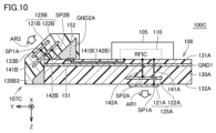
- FIG. 10 is a side perspective view of an antenna module 100C according to the fourth embodiment.
- the antenna module 100C has a configuration in which the antenna block 107 in the antenna module 100 of the first embodiment is replaced with an antenna block 107C. Furthermore, in the antenna module 100C, a radiation electrode 122A and a power supply wiring 142A are added to the main board 108.
- the other configuration of the antenna module 100C is the same as that of the antenna module 100. In FIG. 10, descriptions of elements that overlap with antenna module 100 will not be repeated.
- a radiation electrode 122A is arranged in a layer between the radiation electrode 121A and the ground electrode GND1 on the dielectric substrate 130A, facing the radiation electrode 121A.
- a high frequency signal is transmitted from the RFIC 110 to the radiation electrode 122A via the power supply wiring 142A.
- the power supply wiring 142A extends from the RFIC 110 through the ground electrode GND1 and is connected to the power supply point SP2A of the radiation electrode 122A. Radio waves are radiated from the radiation electrodes 121A and 122A in the positive direction of the Z axis indicated by arrow AR1.
- the antenna block 107C includes a dielectric substrate 130B3, radiation electrodes 121B and 122B, and a ground electrode GND2A.
- the dielectric substrate 130B2 has a rectangular cross section with some corners cut off when viewed in plan from the X-axis direction. More specifically, the dielectric substrate 130B2 has a main surface 133B whose normal direction is an oblique direction between the positive direction of the Y axis and the negative direction of the Z axis.
- the radiation electrodes 121B and 122B are arranged parallel to the main surface 133B on the dielectric substrate 130B3.
- the ground electrode GND2A is a metal body having a surface parallel to the main surface 133B.
- the ground electrode GND2A may have a structure in which a plurality of plate electrodes parallel to the main surface 133B are stacked and these plate electrodes are connected to each other by one or more vias.
- the radiation electrode 122B is arranged between the radiation electrode 121B and the ground electrode GND2A, facing the radiation electrode 121B.
- a high frequency signal from the RFIC 110 is transmitted to the radiation electrodes 121B and 122B via power supply wirings 141B and 142B, respectively.
- the power supply wiring 141B runs from the RFIC 110, passes through the dielectric substrate 130A and the corresponding connection electrodes 151, 152, penetrates the ground electrode GND2A and the radiation electrode 122B in the dielectric substrate 130B3, and reaches the power supply point SP1B of the radiation electrode 121B. connected to.
- the power supply wiring 142B runs from the RFIC 110, passes through the dielectric substrate 130A and the corresponding connection electrodes 151 and 152, penetrates the ground electrode GND2A in the dielectric substrate 130B3, and is connected to the power supply point SP2B of the radiation electrode 122B. .
- radio waves are radiated from the antenna block 107C in the direction of arrow AR3 in FIG.
- the radiation direction of the radio waves radiated from the radiation element 125B (radiation electrodes 121B, 122B) of the antenna block 107C that is, the normal direction of the radiation element 125B (arrow AR3)
- the radiation element 125A (radiation electrodes 121A, 122B) of the main board 108. 122A) that is, the angle formed with the normal direction (arrow AR1) of the radiating element 125A is larger than 90° and smaller than 180°.
- antenna module 100C the coverage range of radio waves radiated from the entire antenna module can be expanded compared to antenna module 100 of Embodiment 1.
- a recess may be formed in a part of the ground electrode GND2A facing the radiation electrode 122B to increase the thickness of the dielectric layer between the radiation electrode 122B and the ground electrode GND2A.
- Embodiment 5 In the antenna module 100 of the first embodiment, a configuration will be described in which the antenna block 107 is arranged along one long side of the dielectric substrate 130A on the main board 108, and the antenna block 107 is used to radiate radio waves in one direction. did. In Embodiment 5, a configuration in which radio waves are radiated in two directions using an antenna block will be described.
- FIG. 11 is a perspective view of an antenna module 100D according to the fifth embodiment.
- the antenna module 100D has a configuration in which an antenna block 107D is further arranged at the end of the dielectric substrate 130A in the positive direction of the X axis. That is, in addition to radiating radio waves in the positive direction of the Y-axis and Z-axis, the antenna block 107D can also radiate radio waves in the positive direction of the X-axis.
- the antenna module 100D a part of the high frequency signal supplied to the antenna block 107 is branched and supplied to the antenna block 107D.
- TRP total radiation power
- EIRP equivalent isotopically radiated power
- CDF cumulative distribution function
- FIG. 12 is a perspective view of a modified antenna module 100E.
- an antenna block 107D is arranged at the end of the dielectric substrate 130A in the positive direction of the X-axis, as in the antenna module 100D of the fifth embodiment, and an antenna block 107D is arranged at the end of the dielectric substrate 130A in the negative direction of the X-axis.
- An antenna block 107E is arranged. Radio waves are radiated from the antenna block 107E in the negative direction of the X-axis.
- the configuration is such that one position of the antenna block 107 in the antenna module 100D is changed to the end in the negative direction of the X axis.
- the size of the SiP module 105E in the X-axis direction is shorter and smaller than that of the antenna module 100, so that the overall dimension of the dielectric substrate 130A in the X-axis direction is shortened. ing.
- An antenna module includes a first substrate on which a flat plate-shaped first radiating element is disposed, and a second substrate on which a flat plate-shaped second radiating element is disposed.
- the first substrate has a first surface and a second surface facing each other.
- the first radiating element is disposed on the second surface of the first substrate or at a position between the first surface and the second surface.
- a recessed portion recessed in the normal direction of the first surface is formed on the first surface of the first substrate.
- the second substrate includes a first region arranged to fit inside the recess and a second region in contact with the first surface of the first substrate. The normal direction of the second radiating element is different from the normal direction of the first radiating element.
- the second substrate includes a connection electrode that is disposed in the second region and enables electrical connection with the first substrate.
- a high frequency signal is transmitted to the second radiating element via the connection electrode.
- the normal direction of the second radiating element is orthogonal to the normal direction of the first radiating element.
- the angle between the normal direction of the second radiating element and the normal direction of the first radiating element is 90°. larger and smaller than 180°.
- the antenna module according to any one of Items 1 to 8 includes a first ground electrode disposed between the first surface and the first radiating element on the first substrate; The device further includes a second ground electrode disposed facing the second radiating element on the two substrates.
- each of the first radiating element and the second radiating element is capable of radiating radio waves in two different polarization directions. .
- the first radiating elements are arranged opposite to each other and are capable of radiating radio waves in the first frequency band. and a second element capable of emitting radio waves in a second frequency band lower than that of the first element.
- the second radiating element is a third element that is arranged to face each other and is capable of radiating radio waves in a third frequency band. and a fourth element capable of emitting radio waves in a fourth frequency band lower than that of the third element.
- the antenna module according to any one of Items 1 to 12 further includes a power feeding device that supplies a high frequency signal to the first radiating element and the second radiating element.
- the power feeding device is disposed on the first surface.
- the antenna module described in Section 1 further includes a power feeding device and power feeding wiring.
- the power supply device supplies a high frequency signal to the first radiating element and the second radiating element.
- the power supply wiring transmits a high frequency signal from the power supply device to the second radiating element.
- the second substrate is disposed in the second region and includes a connection electrode for enabling electrical connection with the first substrate.
- the power supply wiring passes through the first substrate and is connected to the second radiating element via the connection electrode.
- the antenna module according to any one of Items 1 to 15 further includes a third substrate on which a flat third radiating element is arranged.
- the third substrate is arranged adjacent to the second substrate in the first direction.
- the normal direction of the third radiating element is the same as the normal direction of the second radiating element.
- the antenna module according to Item 16 further includes a flat plate-shaped fourth radiating element disposed adjacent to the first radiating element in the first direction on the first substrate.
- the direction perpendicular to the direction from the first region to the first radiating element and along the first surface is In the case of two directions, the second region extends from the first region in the second direction.
- the second region extends in a third direction from the first region toward the first radiating element.
- the antenna module according to any one of Items 1 to 19 further includes a connector disposed on the first surface and for electrically connecting to an external device.
Landscapes
- Waveguide Aerials (AREA)
Abstract
Module d'antenne (100) comprenant un substrat diélectrique (130A) sur lequel une électrode rayonnante de type plaque plate (121A) est disposée, et un substrat diélectrique (130B) sur lequel une électrode rayonnante de type plaque plate (121B) est disposée. Le substrat diélectrique (130A) présente des surfaces principales (131A, 132A) qui se font face. L'électrode rayonnante (121A) est disposée sur la surface principale (131A) ou dans une position entre la surface principale (131A) et la surface principale (132A) dans le substrat diélectrique (130A). Une section d'évidement (170) qui est évidée dans la direction normale de la surface principale (131A) est formée sur la surface principale (131A) du substrat diélectrique (130A). Le substrat diélectrique (130B) comporte une région (RG1) qui est disposée de façon à entrer à l'intérieur de la section d'évidement (170), et une région (RG2) qui est en contact avec la surface principale (131A) du substrat diélectrique (130A). La direction normale de l'électrode rayonnante (121B) est différente de la direction normale de l'électrode rayonnante (121A).
Applications Claiming Priority (2)
| Application Number | Priority Date | Filing Date | Title |
|---|---|---|---|
| JP2022-073406 | 2022-04-27 | ||
| JP2022073406 | 2022-04-27 |
Publications (1)
| Publication Number | Publication Date |
|---|---|
| WO2023210118A1 true WO2023210118A1 (fr) | 2023-11-02 |
Family
ID=88518452
Family Applications (1)
| Application Number | Title | Priority Date | Filing Date |
|---|---|---|---|
| PCT/JP2023/005375 WO2023210118A1 (fr) | 2022-04-27 | 2023-02-16 | Module d'antenne |
Country Status (1)
| Country | Link |
|---|---|
| WO (1) | WO2023210118A1 (fr) |
Citations (2)
| Publication number | Priority date | Publication date | Assignee | Title |
|---|---|---|---|---|
| JP2010245893A (ja) * | 2009-04-07 | 2010-10-28 | Murata Mfg Co Ltd | アンテナの取り付け構造 |
| WO2020170722A1 (fr) * | 2019-02-20 | 2020-08-27 | 株式会社村田製作所 | Module d'antenne, dispositif de communication sur lequel un module d'antenne est monté, et procédé de fabrication de module d'antenne |
-
2023
- 2023-02-16 WO PCT/JP2023/005375 patent/WO2023210118A1/fr unknown
Patent Citations (2)
| Publication number | Priority date | Publication date | Assignee | Title |
|---|---|---|---|---|
| JP2010245893A (ja) * | 2009-04-07 | 2010-10-28 | Murata Mfg Co Ltd | アンテナの取り付け構造 |
| WO2020170722A1 (fr) * | 2019-02-20 | 2020-08-27 | 株式会社村田製作所 | Module d'antenne, dispositif de communication sur lequel un module d'antenne est monté, et procédé de fabrication de module d'antenne |
Similar Documents
| Publication | Publication Date | Title |
|---|---|---|
| US11581635B2 (en) | Antenna module | |
| WO2020261806A1 (fr) | Module d'antenne et dispositif de communication doté de celui-ci | |
| US11631936B2 (en) | Antenna device | |
| WO2020145392A1 (fr) | Module d'antenne et dispositif de communication sur lequel est monté un module d'antenne | |
| CN114521307A (zh) | 天线模块和搭载该天线模块的通信装置以及电路基板 | |
| WO2022224650A1 (fr) | Module d'antenne | |
| US20220181794A1 (en) | Antenna device, antenna module, and communication device | |
| JP6798656B1 (ja) | アンテナモジュールおよびそれを搭載した通信装置 | |
| US11916312B2 (en) | Antenna module, communication device mounting the same, and circuit board | |
| US20220368031A1 (en) | Antenna module | |
| WO2023210118A1 (fr) | Module d'antenne | |
| JP7283623B2 (ja) | アンテナモジュールおよびそれを搭載した通信装置 | |
| WO2023157450A1 (fr) | Module d'antenne et dispositif de communication avec ce module d'antenne monté dessus | |
| WO2021019899A1 (fr) | Dispositif d'antenne, module d'antenne et dispositif de communication | |
| WO2023037805A1 (fr) | Module d'antenne et dispositif de communication équipé de celui-ci | |
| WO2022185874A1 (fr) | Module d'antenne et dispositif de communication équipé de ce dernier | |
| JP7294525B2 (ja) | アンテナモジュールおよびそれを搭載する通信装置 | |
| US20220085521A1 (en) | Antenna module and communication device equipped with the same | |
| WO2024075334A1 (fr) | Module d'antenne et dispositif de communication en étant doté | |
| WO2024034188A1 (fr) | Module d'antenne et dispositif de communication équipé de celui-ci | |
| WO2023047801A1 (fr) | Module d'antenne et dispositif de communication équipé de celui-ci | |
| WO2022004111A1 (fr) | Module d'antenne et dispositif de communication équipé de celui-ci | |
| WO2022230383A1 (fr) | Module d'antenne et dispositif de communication équipé de celui-ci | |
| WO2023037806A1 (fr) | Module d'antenne et dispositif de communication à module d'antenne monté sur celui-ci | |
| WO2023095643A1 (fr) | Module d'antenne et dispositif de communication équipé de celui-ci |
Legal Events
| Date | Code | Title | Description |
|---|---|---|---|
| 121 | Ep: the epo has been informed by wipo that ep was designated in this application |
Ref document number: 23795866 Country of ref document: EP Kind code of ref document: A1 |