WO2023210118A1 - Antenna module - Google Patents
Antenna module Download PDFInfo
- Publication number
- WO2023210118A1 WO2023210118A1 PCT/JP2023/005375 JP2023005375W WO2023210118A1 WO 2023210118 A1 WO2023210118 A1 WO 2023210118A1 JP 2023005375 W JP2023005375 W JP 2023005375W WO 2023210118 A1 WO2023210118 A1 WO 2023210118A1
- Authority
- WO
- WIPO (PCT)
- Prior art keywords
- substrate
- radiating element
- antenna module
- module according
- antenna
- Prior art date
Links
- 239000000758 substrate Substances 0.000 claims abstract description 174
- 230000010287 polarization Effects 0.000 claims description 9
- 230000005855 radiation Effects 0.000 description 110
- 238000004891 communication Methods 0.000 description 12
- 101100489717 Saccharomyces cerevisiae (strain ATCC 204508 / S288c) GND2 gene Proteins 0.000 description 10
- 238000010586 diagram Methods 0.000 description 10
- 239000011347 resin Substances 0.000 description 9
- 229920005989 resin Polymers 0.000 description 9
- 101100489713 Saccharomyces cerevisiae (strain ATCC 204508 / S288c) GND1 gene Proteins 0.000 description 7
- 239000010410 layer Substances 0.000 description 7
- 230000004048 modification Effects 0.000 description 6
- 238000012986 modification Methods 0.000 description 6
- 238000010030 laminating Methods 0.000 description 4
- 229920000106 Liquid crystal polymer Polymers 0.000 description 2
- 239000004977 Liquid-crystal polymers (LCPs) Substances 0.000 description 2
- 239000000919 ceramic Substances 0.000 description 2
- 230000008878 coupling Effects 0.000 description 2
- 238000010168 coupling process Methods 0.000 description 2
- 238000005859 coupling reaction Methods 0.000 description 2
- 230000009977 dual effect Effects 0.000 description 2
- 230000000694 effects Effects 0.000 description 2
- 238000000034 method Methods 0.000 description 2
- 229920000139 polyethylene terephthalate Polymers 0.000 description 2
- 239000005020 polyethylene terephthalate Substances 0.000 description 2
- 239000004593 Epoxy Substances 0.000 description 1
- -1 Polyethylene Terephthalate Polymers 0.000 description 1
- 239000004642 Polyimide Substances 0.000 description 1
- 230000005540 biological transmission Effects 0.000 description 1
- 230000015572 biosynthetic process Effects 0.000 description 1
- 230000001186 cumulative effect Effects 0.000 description 1
- 230000007423 decrease Effects 0.000 description 1
- 230000006866 deterioration Effects 0.000 description 1
- 238000005315 distribution function Methods 0.000 description 1
- 239000000463 material Substances 0.000 description 1
- 239000002184 metal Substances 0.000 description 1
- 230000010363 phase shift Effects 0.000 description 1
- 229920001721 polyimide Polymers 0.000 description 1
- 239000002356 single layer Substances 0.000 description 1
- 229910000679 solder Inorganic materials 0.000 description 1
- 238000003786 synthesis reaction Methods 0.000 description 1
Images


Classifications
-
- H—ELECTRICITY
- H01—ELECTRIC ELEMENTS
- H01Q—ANTENNAS, i.e. RADIO AERIALS
- H01Q1/00—Details of, or arrangements associated with, antennas
- H01Q1/52—Means for reducing coupling between antennas; Means for reducing coupling between an antenna and another structure
-
- H—ELECTRICITY
- H01—ELECTRIC ELEMENTS
- H01Q—ANTENNAS, i.e. RADIO AERIALS
- H01Q13/00—Waveguide horns or mouths; Slot antennas; Leaky-waveguide antennas; Equivalent structures causing radiation along the transmission path of a guided wave
- H01Q13/08—Radiating ends of two-conductor microwave transmission lines, e.g. of coaxial lines, of microstrip lines
-
- H—ELECTRICITY
- H01—ELECTRIC ELEMENTS
- H01Q—ANTENNAS, i.e. RADIO AERIALS
- H01Q21/00—Antenna arrays or systems
- H01Q21/24—Combinations of antenna units polarised in different directions for transmitting or receiving circularly and elliptically polarised waves or waves linearly polarised in any direction
-
- H—ELECTRICITY
- H01—ELECTRIC ELEMENTS
- H01Q—ANTENNAS, i.e. RADIO AERIALS
- H01Q21/00—Antenna arrays or systems
- H01Q21/28—Combinations of substantially independent non-interacting antenna units or systems
-
- H—ELECTRICITY
- H01—ELECTRIC ELEMENTS
- H01Q—ANTENNAS, i.e. RADIO AERIALS
- H01Q21/00—Antenna arrays or systems
- H01Q21/30—Combinations of separate antenna units operating in different wavebands and connected to a common feeder system
-
- H—ELECTRICITY
- H01—ELECTRIC ELEMENTS
- H01Q—ANTENNAS, i.e. RADIO AERIALS
- H01Q23/00—Antennas with active circuits or circuit elements integrated within them or attached to them
Definitions
- the present disclosure relates to an antenna module, and more specifically, to a technique for downsizing an antenna module that can radiate radio waves in two directions.
- Patent Document 1 discloses an antenna module having a bent dielectric substrate, in which radiating elements are arranged on two surfaces with different normal directions. .
- Patent Document 1 The antenna module disclosed in US Pat. No. 1,110,8157 (Patent Document 1) may be used, for example, in a communication device typified by a mobile terminal such as a mobile phone or a smartphone. It is desired that such communication devices be further miniaturized and thinner, and along with this, the antenna modules installed in such communication devices are also required to be further miniaturized and lower in profile. .
- the present disclosure has been made in order to solve the above-mentioned problems, and the purpose is to achieve a reduction in height while ensuring mechanical strength in an antenna module that can radiate radio waves in two directions. That's true.
- the antenna module includes a first substrate on which a flat plate-shaped first radiating element is arranged, and a second substrate on which a flat plate-shaped second radiating element is arranged.
- the first substrate has a first surface and a second surface facing each other.
- the first radiating element is disposed on the second surface of the first substrate or at a position between the first surface and the second surface.
- a recessed portion recessed in the normal direction of the first surface is formed on the first surface of the first substrate.
- the second substrate includes a first region arranged to fit inside the recess and a second region in contact with the first surface of the first substrate.
- the normal direction of the second radiating element is different from the normal direction of the first radiating element.
- the second substrate on which the second radiating element having a different radiation direction (normal direction) is disposed is fitted into the recess formed in the first substrate on which the first radiating element is disposed.
- the second substrate is fixed on the main surface (first surface) of the first substrate.
- FIG. 1 is a block diagram of a communication device to which the antenna module according to Embodiment 1 is applied.
- FIG. FIG. 2 is a perspective view of the antenna module of FIG. 1;
- FIG. 2 is a side perspective view of the antenna module of FIG. 1;
- FIG. 3 is a diagram for explaining an antenna block. It is a figure for explaining the antenna block of a modification.
- FIG. 3 is a side perspective view of an antenna module according to a second embodiment.
- FIG. 3 is a diagram for explaining antenna characteristics of a radiating element on the main board side in the antenna modules of Embodiment 1 and Embodiment 2;
- FIG. 7 is a side perspective view of an antenna module according to Embodiment 3;
- FIG. 7 is a diagram for explaining antenna characteristics of a radiating element on the antenna block side in the antenna modules of Embodiment 2 and Embodiment 3;
- FIG. 7 is a side perspective view of an antenna module according to Embodiment 4.
- FIG. 7 is a perspective view of an antenna module according to a fifth embodiment. It is a perspective view of the antenna module of a modification.
- FIG. 1 is a block diagram of a communication device 10 to which an antenna module 100 according to the present embodiment is applied.
- the communication device 10 is, for example, a mobile terminal such as a mobile phone, a smartphone, or a tablet, or a personal computer with a communication function.
- An example of the frequency band of radio waves used in the antenna module 100 according to the present embodiment is, for example, radio waves in the millimeter wave band with center frequencies of 28 GHz, 39 GHz, and 60 GHz, but radio waves in frequency bands other than the above may also be used. Applicable.
- communication device 10 includes an antenna module 100 and a BBIC 200 that constitutes a baseband signal processing circuit.
- the antenna module 100 includes an RFIC 110, which is an example of a power feeding device, and an antenna device 120.
- the communication device 10 up-converts the signal transmitted from the BBIC 200 to the antenna module 100 into a high-frequency signal and radiates it from the antenna device 120, and down-converts the high-frequency signal received by the antenna device 120 and processes the signal in the BBIC 200. do.
- the antenna device 120 includes a dielectric substrate 130A and a plurality of dielectric substrates 130B.
- a plurality of radiating elements 125A are arranged on the dielectric substrate 130A.
- Each radiation element 125A includes a radiation electrode 121A and a radiation electrode 122A having a flat plate shape.
- a radiating element 125B is arranged on each dielectric substrate 130B.
- the radiation element 125B includes a radiation electrode 121B and a radiation electrode 122B each having a flat plate shape.
- Each radiation electrode included in the radiation elements 125A and 125B is a flat patch antenna having a circular, elliptical, or polygonal shape.
- each radiation electrode is a microstrip antenna having a substantially square shape.
- the size of the radiation electrode 121A is smaller than the size of the radiation electrode 122A. Therefore, the frequency band of the radio waves radiated from the radiation electrode 121A is higher than the frequency band of the radio waves radiated from the radiation electrode 122A.
- the size of the radiation electrode 121B is smaller than the size of the radiation electrode 122B, and the frequency band of the radio waves radiated from the radiation electrode 121B is higher than the frequency band of the radio waves radiated from the radiation electrode 122B.
- the antenna module 100 in the example of FIG. 1 is a so-called dual-band type antenna module that can radiate radio waves in two different frequency bands from each of the two dielectric substrates 130A and 130B.
- the dielectric substrate 130A on which the plurality of radiating elements 125A are arranged is also referred to as the "main board 108", and the configuration of each dielectric substrate 130B on which the radiating elements 125B are arranged is referred to as the "antenna block 107". ” is also called.
- the antenna device 120 has a configuration in which a plurality of antenna blocks 107 are attached to the main board 108.
- FIG. 1 an example of a configuration is shown in which the antenna device 120 includes four dielectric substrates 130B, and four radiating elements 125A are arranged on the dielectric substrate 130A.
- the number of elements 125A is not limited to this.
- FIG. 1 shows an example in which the radiating elements 125A are arranged in a one-dimensional array on the dielectric substrate 130A, two radiating elements 125A are arranged on the dielectric substrate 130A. They may be arranged in a dimensional array. Alternatively, a configuration may be adopted in which a single radiating element 125A is disposed on the dielectric substrate 130A.
- the RFIC 110 includes four power supply circuits 110A to 110D.
- the power supply circuit 110A is a circuit for supplying a high frequency signal to the radiation electrode 121A on the main board 108 side.
- the power supply circuit 110B is a circuit for supplying a high frequency signal to the radiation electrode 122A on the main board 108 side.
- the feed circuit 110C is a circuit for supplying a high frequency signal to the radiation electrode 122B on the antenna block 107 side.
- the feeding circuit 110D is a circuit for supplying a high frequency signal to the radiation electrode 121B on the antenna block 107 side. Note that since the internal configuration of the power supply circuits 110A to 110D is common, in order to simplify the explanation, in FIG. Omitted. Below, the function of the power supply circuit 110A will be explained as a representative.
- the power supply circuit 110A includes switches 111A to 111D, 113A to 113D, 117, power amplifiers 112AT to 112DT, low noise amplifiers 112AR to 112DR, attenuators 114A to 114D, phase shifters 115A to 115D, and signal synthesis/distribution. 116, a mixer 118, and an amplifier circuit 119.
- the switches 111A to 111D and 113A to 113D are switched to the power amplifiers 112AT to 112DT, and the switch 117 is connected to the transmitting side amplifier of the amplifier circuit 119.
- the switches 111A to 111D and 113A to 113D are switched to the low noise amplifiers 112AR to 112DR, and the switch 117 is connected to the receiving amplifier of the amplifier circuit 119.
- the intermediate frequency signal transmitted from the BBIC 200 is amplified by the amplifier circuit 119 and up-converted by the mixer 118.
- the transmission signal which is an up-converted high-frequency signal, is divided into four waves by the signal combiner/distributor 116, passes through corresponding signal paths, and is fed to different radiation electrodes 121A.
- the degree of phase shift of the phase shifters 115A to 115D arranged in each signal path By individually adjusting the degree of phase shift of the phase shifters 115A to 115D arranged in each signal path, the directivity of the radio waves output from the radiation electrode 121A can be adjusted.
- the received signal which is a high-frequency signal received by each radiation electrode 121A, is transmitted to the power supply circuit 110A of the RFIC 110, and multiplexed in the signal combiner/distributor 116 via four different signal paths.
- the multiplexed received signal is down-converted by mixer 118, further amplified by amplifier circuit 119, and transmitted to BBIC 200.
- the RFIC 110 is formed, for example, as a one-chip integrated circuit component including the circuit configuration described above.
- each feed circuit may be formed as a separate integrated circuit component.
- the equipment (switch, power amplifier, low noise amplifier, attenuator, phase shifter) corresponding to each radiating element may be formed as a one-chip integrated circuit component for each corresponding radiating element.
- FIG. 2 is a perspective view of the antenna module 100 according to the first embodiment.
- the upper part (A) shows a state in which the main board 108 and the antenna block 107 are separated.
- the lower part (B) of FIG. 2 shows a state in which the antenna block 107 is attached to the main board 108.
- FIG. 3 is a side perspective view of the antenna module 100 viewed from the positive direction of the X-axis in the state shown in FIG. 2(B).
- FIG. 4 is a perspective view of the antenna block 107 alone.
- FIG. 4 is a perspective view of the antenna block 107 when the plane in the Y-axis direction is the front. Further, the lower part (B) of FIG. 4 is a perspective view of the antenna block 107 when the surface in the Z-axis direction is the front.
- the radiation element 125A has a single radiation electrode 121A
- the radiation element 125B has a single radiation electrode 121B.
- five radiating elements are arranged on the dielectric substrate 130A, and five antenna blocks 107 are provided correspondingly.
- the antenna module 100 includes, in addition to dielectric substrates 130A, 130B, radiation electrodes 121A, 121B, and RFIC 110, power supply wiring 141A, 141B, connection electrodes 151, 152, and ground electrode GND1, Further includes GND2.
- the normal direction of the main surface of the dielectric substrate 130A will be referred to as the Z-axis direction.
- the arrangement direction of the radiation electrode 121A and the antenna block 107 is defined as the X axis, and the direction orthogonal to the X axis is defined as the Y axis.
- the radiation direction of the radio waves from the radiation electrode 121A is the positive direction of the Z-axis
- the radiation direction of the radio waves from the radiation electrode 121B is the positive direction of the Y-axis. That is, the normal direction of the radiation electrode 121A and the normal direction of the radiation electrode 121B are orthogonal.
- the dielectric substrates 130A and 130B are, for example, low temperature co-fired ceramics (LTCC) multilayer substrates, multilayer resin substrates formed by laminating a plurality of resin layers made of resin such as epoxy or polyimide. , a multilayer resin substrate formed by laminating multiple resin layers made of liquid crystal polymer (LCP) with a lower dielectric constant, and a multilayer resin substrate formed by laminating multiple resin layers made of fluororesin.
- LCP liquid crystal polymer
- the dielectric substrate 130A of the main substrate 108 has a substantially rectangular shape with the long side in the X-axis direction when viewed from the Z-axis direction.
- a plurality of recesses (notches) 170 are formed on one long side of the dielectric substrate 130A along the X-axis (the end in the positive direction of the Y-axis).
- the recess 170 is formed up to the side surface (end) of the dielectric substrate 130A in the positive direction of the Y-axis, and penetrates in the Z-axis direction.
- the antenna block 107 is partially fitted into the recessed portion of the recess 170 and fixed. Note that the recessed portion 170 does not necessarily have to penetrate the dielectric substrate 130A in the Z-axis direction as shown in FIG. 2, but only needs to be recessed in the Z-axis direction from the main surface 131A. Furthermore, the position of the recess 170 does not have to be at the end of the dielectric substrate 130A.
- connection electrode 151 is arranged at a portion of the main surface 131A that is in contact with the antenna block 107. This connection electrode 151 is used for electrical connection between the antenna block 107 and the main board 108.
- the dielectric substrate 130A has a main surface 132A located in the positive direction of the Z-axis and a main surface 131A located in the negative direction of the Z-axis.
- a plurality of radiation electrodes 121A are arranged in a row in the X-axis direction on or inside the main surface 132A of the dielectric substrate 130A.
- Mounted on the main surface 131A is an SiP (System In Package) module 105 that includes an RFIC 110, a power module IC (not shown), etc., and a connector 106 used for connection with external equipment.
- a ground electrode GND1 is arranged to face the radiation electrode 121A over the entire surface.
- a high frequency signal is supplied from the RFIC 110 to each radiation electrode 121A through a power supply wiring 141A.
- the power supply wiring 141A passes through the ground electrode GND1 in the dielectric substrate 130A and is connected to the power supply point SP1A of the radiation electrode 121A.
- the feed point SP1A is arranged at a position offset from the center of the radiation electrode 121A in the negative direction of the Y-axis. Therefore, radio waves whose polarization direction is in the Y-axis direction are radiated from the radiation electrode 121A in the positive direction of the Z-axis.
- the dielectric substrate 130B of the antenna block 107 includes a region RG1 at the center where the radiation electrode 121B is arranged, and a region RG2 protruding from the region RG1 in the positive and negative directions of the X axis. and has.
- the dimension of region RG2 in the Z-axis direction is shorter than the dimension of region RG1 in the Z-axis direction. That is, the dielectric substrate 130B has a substantially T-shape when viewed from above in the Y-axis direction. As shown in FIG.
- the dielectric substrate 130B is arranged such that the region RG1 enters into the recess 170 of the dielectric substrate 130B, and the surface of the region RG2 in the positive direction of the Z axis is aligned with the dielectric substrate 130A. It is arranged so that it may be in contact with main surface 131A of.
- a radiation electrode 121B is arranged on the main surface 131B of the dielectric substrate 130B in the positive direction of the Y-axis. Further, in the dielectric substrate 130B, a ground electrode GND2 facing the radiation electrode 121B is arranged at a position close to the main surface 132B in the negative direction of the Y-axis over the entire area RG1.
- connection electrode 152 is arranged on the surface in the positive direction of the Z-axis in the region RG2 of the dielectric substrate 130B.
- the connection electrode 152 is arranged at a position in contact with the connection electrode 151 arranged on the main surface 131A on the main board 108 side when the antenna block 107 is fitted into the main board 108.
- Connection electrode 151 and connection electrode 152 are electrically connected, for example, by solder. Note that the electrical coupling between the connection electrode 151 and the connection electrode 152 is not limited to direct connection, and may be capacitive coupling in which the electrodes are not in contact with each other.
- a high frequency signal is transmitted from the RFIC 110 to the radiation electrode 121B of the antenna block 107 via the power supply wiring 141B.
- the power supply wiring 141B is connected to the power supply point SP1B of the radiation electrode 121B from the RFIC 110, passing through the dielectric substrate 130A, the connection electrodes 151, 152, and the dielectric substrate 130B.
- the feed point SP1B is arranged at a position offset from the center of the radiation electrode 121B in the negative direction of the Z-axis. Therefore, radio waves whose polarization direction is in the Z-axis direction are radiated from the radiation electrode 121B in the positive direction of the Y-axis.
- the antenna block 107 is arranged at a distance d1 from the radiation electrode 121A of the main board 108 in the Y-axis direction. Note that, assuming that the wavelength of the radio waves radiated from the radiation electrode 121A is ⁇ , it is possible to radiate radio waves in two directions if the distance d1 is set to at least 0.05 ⁇ or more.
- the main surface 131B of the dielectric substrate 130B of the antenna block 107 does not protrude from the end of the dielectric substrate 130A in the positive direction of the Y axis. In other words, when the dielectric substrate 130A is viewed from the normal direction (Z-axis direction), the dielectric substrate 130B of the antenna block 107 is positioned inside the outermost end of the dielectric substrate 130A. It is located.
- Patent Document 1 When an antenna module capable of emitting radio waves in two directions is realized using a bent dielectric substrate as disclosed in the above-mentioned US Pat. No. 1,110,157 (Patent Document 1), one of the bent sides Since the amount of protrusion of one substrate from the other substrate tends to be large, dimensional limitations may occur when further reducing the height. In addition, the position and number of bent parts that connect two substrate surfaces are limited, and the dielectric thickness of the bent parts needs to be thinned, so it may not be possible to obtain sufficient mechanical strength at the bent parts, or multiple When a radiation electrode is used, there is a possibility that a passage route for the power supply wiring cannot be secured.
- the antenna block 107 in which one radiation electrode 121B is arranged on another dielectric substrate 130B is used, and the antenna block 107 is fitted into the recess 170 of the main substrate 108.
- the antenna block 107 is configured to be fixed on the main surface 131A of the main board 108.
- the antenna block 107 can be configured with a separate dielectric substrate, the dielectric thickness (i.e., the distance between the radiation electrode 121B and the ground electrode GND2) can be ensured, thereby reducing the amount of radio waves radiated. Antenna characteristics such as frequency band can be improved.
- the dielectric constant of the dielectric substrate 130B of the antenna block 107 larger than the dielectric constant of the dielectric substrate 130A on the main board 108 side, the radiation electrode 121B and the overall size of the antenna block 107, it is possible to further reduce the height and size.
- FIGS. 2 to 4 above in order to simplify the explanation, the configuration of a single-band type antenna module in which only the radiation electrodes 121 and 121B are arranged as radiating elements has been described, but as shown in FIG. A similar configuration can also be applied to a dual band type configuration in which radiation electrodes of different sizes are stacked on each dielectric substrate. Further, the above configuration is also applicable to a dual polarization type antenna module that can radiate radio waves in two different polarization directions from each radiation electrode.
- radiating element 125A and “radiating element 125B” in Embodiment 1 correspond to “first radiating element” and “second radiating element” in the present disclosure, respectively.
- Radiating electrode 121A” and “radiation electrode 122A” in Embodiment 1 correspond to the "first element” and “second element” in the present disclosure, respectively.
- Radiation electrode 121B” and “radiation electrode 122B” in Embodiment 1 correspond to the "third element” and “fourth element” in the present disclosure, respectively.
- one of the adjacent radiating elements 125A corresponds to the "first radiating element” in the present disclosure, and the other corresponds to the "third radiating element” in the present disclosure.
- one of the adjacent radiating elements 125B corresponds to a “second radiating element” in the present disclosure, and the other corresponds to a “fourth radiating element” in the present disclosure.
- the "X-axis direction” in Embodiment 1 corresponds to the "first direction” and “second direction” in the present disclosure.
- the "Y-axis direction” in the first embodiment corresponds to the "third direction” in the present disclosure.
- “Dielectric substrate 130A” and “dielectric substrate 130B” in Embodiment 1 correspond to “first substrate” and “second substrate” in the present disclosure, respectively.
- “Main surface 131A” and “principal surface 132A” in Embodiment 1 correspond to “first surface” and “second surface” in the present disclosure, respectively.
- “Regions RG1 and RG2” in Embodiment 1 correspond to the “first region” and “second region” in the present disclosure, respectively.
- “Ground electrodes GND1 and GND2" in the first embodiment correspond to the "first ground electrode” and “second ground electrode” in the present disclosure, respectively.
- FIG. 5 is a diagram for explaining a modification of the antenna block 107A. Similar to FIG. 4, the upper part (A) of FIG. 5 is a perspective view of the antenna block 107A when the plane in the Y-axis direction is the front, and the lower part (B) of FIG. FIG.
- antenna block 107A differs from antenna block 107 in FIG. 4 in the configuration of region RG2 for fixing to main surface 131A of main board 108. More specifically, in place of the region RG2 of the antenna block 107, the dielectric substrate 130B1 in the antenna block 107A extends from the back surface (i.e., the main surface in the negative direction of the Y-axis) of the region RG1 where the radiation electrode 121B is arranged. It has a protruding region RG2A. In other words, the dielectric substrate 130B1 has a substantially L-shape when viewed in plan from the X-axis direction. The connection electrode 152 is arranged on the surface of the region RG2A in the positive direction of the Z axis.
- the region RG2A is fixed to the dielectric substrate 130A at the main surface 131A at a position from the recess 170 toward the SiP 105.
- dielectric substrate 130B1 in the modification corresponds to the "second substrate” in the present disclosure.
- FIG. 6 is a side perspective view of the antenna module 100A according to the second embodiment.
- the antenna module 100A is different from the antenna module 100 of the first embodiment in that the antenna block 107 is disposed at a position protruding from the main board 108.
- the description of the configuration that overlaps with the antenna module 100 of Embodiment 1 will not be repeated.
- antenna block 107 in antenna module 100A is placed at a position spaced apart from radiation electrode 121A by d2 (>d1) in the positive direction of the Y-axis.
- d2 >d1
- a part of the dielectric substrate 130B in the antenna block 107 is positioned in the positive direction of the Y-axis rather than the end in the positive direction of the Y-axis (i.e., the outermost edge) of the dielectric substrate 130A of the main board 108. It stands out.
- a ground electrode GND2 is arranged on the dielectric substrate 130B of the antenna block 107. Therefore, if the distance between the radiation electrode 121A and the dielectric substrate 130B is short, the electric force lines generated from the radiation electrode 121A will be may interfere with the ground electrode GND2 and affect antenna characteristics.
- a part of the antenna block 107 is arranged to protrude from the main board 108 to reduce the distance between the radiation electrode 121A and the ground electrode GND2. By ensuring the distance, deterioration of the antenna characteristics of the radiation electrode 121A can be suppressed.
- FIG. 7 is a diagram for explaining the antenna characteristics of the radiation electrode 121A on the main board 108 side in the antenna module 100 of the first embodiment and the antenna module 100A of the second embodiment.
- a schematic configuration diagram of the antenna module (upper row), a graph of the antenna gain of the radiation electrode 121A (middle row), and a Z The peak gain value in the axial direction (lower row) is shown.
- Radio waves are radiated from the radiation electrode 121A in the positive direction of the Z-axis (direction of arrow AR1 in FIG. 7).
- the peak gain in the first embodiment is 3.28 [dBi], while the peak gain in the second embodiment is 5.16 [dBi]. Therefore, the gain characteristics of the radiation electrode 121A are improved by increasing the distance between the radiation electrode 121A and the antenna block 107.
- the dimension in the Y-axis direction is larger than that of the antenna module 100, so this has the opposite effect from the viewpoint of miniaturization. That is, there is a trade-off relationship between antenna characteristics and miniaturization. Therefore, which configuration of the antenna module 100 or 100A to adopt is appropriately selected in consideration of the required specifications.
- Embodiment 3 In Embodiment 3, a configuration for improving the antenna characteristics of the radiating element on the antenna block 107 side will be described.
- FIG. 8 is a side perspective view of the antenna module 100B according to the third embodiment.
- the antenna module 100B has a configuration in which the antenna block 107A of the antenna module 100A of the second embodiment is replaced with an antenna block 107B.
- the rest of the configuration of antenna module 100B is the same as antenna module 100A.
- the description of the configuration that overlaps with that of the antenna module 100A of the second embodiment will not be repeated.
- the dimension of dielectric substrate 130B2 in the Z-axis direction is longer than dielectric substrate 130B of antenna block 107.
- the dimension of the ground electrode GND2 in the Z-axis direction is also increased.
- the dielectric substrate 130B2 is arranged so as to protrude from the dielectric substrate 130A of the main substrate 108 in the positive and negative directions of the Z-axis. In other words, the dielectric substrate 130B2 protrudes from the main surfaces 131A and 132A of the dielectric substrate 130A in the Z-axis direction, which is the normal direction.
- the dimension of the dielectric substrate of the antenna block in the Z-axis direction is extremely short compared to the X-axis direction. ing. Therefore, the antenna characteristics of radio waves whose polarization direction is in the Z-axis direction are more likely to deteriorate than those of radio waves whose polarization direction is in the X-axis direction.
- the dimensions of the dielectric substrate 130B2 in the Z-axis direction may be changed as in the antenna module 100B of the second embodiment. By increasing the size, antenna characteristics can be adjusted.
- the dimension of the entire antenna module 100B in the Z-axis direction is larger than that of the antenna module 100A, so this has the opposite effect from the viewpoint of miniaturization. . Therefore, which configuration of the antenna modules 100A and 100B to adopt is appropriately selected in consideration of the required specifications.
- FIG. 9 is a diagram for explaining the antenna characteristics of the radiating element on the antenna block side in the antenna module 100A of the second embodiment and the antenna module 100B of the third embodiment.
- FIG. 9 also shows a schematic configuration diagram of the antenna module (upper row) and a graph of the antenna gain of the radiation electrode 121B for the second embodiment (left column) and the third embodiment (right column). (middle row) and the peak gain value in the Y-axis direction (lower row). Radio waves are radiated from the radiation electrode 121B in the positive direction of the Y-axis (direction of arrow AR2 in FIG. 9).
- the peak gain in the second embodiment is 2.23 [dBi]
- the peak gain in the third embodiment is 2.57 [dBi].
- the gain characteristics of the radiation electrode 121B are improved.
- Embodiment 4 In Embodiment 4, a configuration in which the directions of radio waves radiated from the antenna block are different will be described.
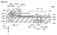
- FIG. 10 is a side perspective view of an antenna module 100C according to the fourth embodiment.
- the antenna module 100C has a configuration in which the antenna block 107 in the antenna module 100 of the first embodiment is replaced with an antenna block 107C. Furthermore, in the antenna module 100C, a radiation electrode 122A and a power supply wiring 142A are added to the main board 108.
- the other configuration of the antenna module 100C is the same as that of the antenna module 100. In FIG. 10, descriptions of elements that overlap with antenna module 100 will not be repeated.
- a radiation electrode 122A is arranged in a layer between the radiation electrode 121A and the ground electrode GND1 on the dielectric substrate 130A, facing the radiation electrode 121A.
- a high frequency signal is transmitted from the RFIC 110 to the radiation electrode 122A via the power supply wiring 142A.
- the power supply wiring 142A extends from the RFIC 110 through the ground electrode GND1 and is connected to the power supply point SP2A of the radiation electrode 122A. Radio waves are radiated from the radiation electrodes 121A and 122A in the positive direction of the Z axis indicated by arrow AR1.
- the antenna block 107C includes a dielectric substrate 130B3, radiation electrodes 121B and 122B, and a ground electrode GND2A.
- the dielectric substrate 130B2 has a rectangular cross section with some corners cut off when viewed in plan from the X-axis direction. More specifically, the dielectric substrate 130B2 has a main surface 133B whose normal direction is an oblique direction between the positive direction of the Y axis and the negative direction of the Z axis.
- the radiation electrodes 121B and 122B are arranged parallel to the main surface 133B on the dielectric substrate 130B3.
- the ground electrode GND2A is a metal body having a surface parallel to the main surface 133B.
- the ground electrode GND2A may have a structure in which a plurality of plate electrodes parallel to the main surface 133B are stacked and these plate electrodes are connected to each other by one or more vias.
- the radiation electrode 122B is arranged between the radiation electrode 121B and the ground electrode GND2A, facing the radiation electrode 121B.
- a high frequency signal from the RFIC 110 is transmitted to the radiation electrodes 121B and 122B via power supply wirings 141B and 142B, respectively.
- the power supply wiring 141B runs from the RFIC 110, passes through the dielectric substrate 130A and the corresponding connection electrodes 151, 152, penetrates the ground electrode GND2A and the radiation electrode 122B in the dielectric substrate 130B3, and reaches the power supply point SP1B of the radiation electrode 121B. connected to.
- the power supply wiring 142B runs from the RFIC 110, passes through the dielectric substrate 130A and the corresponding connection electrodes 151 and 152, penetrates the ground electrode GND2A in the dielectric substrate 130B3, and is connected to the power supply point SP2B of the radiation electrode 122B. .
- radio waves are radiated from the antenna block 107C in the direction of arrow AR3 in FIG.
- the radiation direction of the radio waves radiated from the radiation element 125B (radiation electrodes 121B, 122B) of the antenna block 107C that is, the normal direction of the radiation element 125B (arrow AR3)
- the radiation element 125A (radiation electrodes 121A, 122B) of the main board 108. 122A) that is, the angle formed with the normal direction (arrow AR1) of the radiating element 125A is larger than 90° and smaller than 180°.
- antenna module 100C the coverage range of radio waves radiated from the entire antenna module can be expanded compared to antenna module 100 of Embodiment 1.
- a recess may be formed in a part of the ground electrode GND2A facing the radiation electrode 122B to increase the thickness of the dielectric layer between the radiation electrode 122B and the ground electrode GND2A.
- Embodiment 5 In the antenna module 100 of the first embodiment, a configuration will be described in which the antenna block 107 is arranged along one long side of the dielectric substrate 130A on the main board 108, and the antenna block 107 is used to radiate radio waves in one direction. did. In Embodiment 5, a configuration in which radio waves are radiated in two directions using an antenna block will be described.
- FIG. 11 is a perspective view of an antenna module 100D according to the fifth embodiment.
- the antenna module 100D has a configuration in which an antenna block 107D is further arranged at the end of the dielectric substrate 130A in the positive direction of the X axis. That is, in addition to radiating radio waves in the positive direction of the Y-axis and Z-axis, the antenna block 107D can also radiate radio waves in the positive direction of the X-axis.
- the antenna module 100D a part of the high frequency signal supplied to the antenna block 107 is branched and supplied to the antenna block 107D.
- TRP total radiation power
- EIRP equivalent isotopically radiated power
- CDF cumulative distribution function
- FIG. 12 is a perspective view of a modified antenna module 100E.
- an antenna block 107D is arranged at the end of the dielectric substrate 130A in the positive direction of the X-axis, as in the antenna module 100D of the fifth embodiment, and an antenna block 107D is arranged at the end of the dielectric substrate 130A in the negative direction of the X-axis.
- An antenna block 107E is arranged. Radio waves are radiated from the antenna block 107E in the negative direction of the X-axis.
- the configuration is such that one position of the antenna block 107 in the antenna module 100D is changed to the end in the negative direction of the X axis.
- the size of the SiP module 105E in the X-axis direction is shorter and smaller than that of the antenna module 100, so that the overall dimension of the dielectric substrate 130A in the X-axis direction is shortened. ing.
- An antenna module includes a first substrate on which a flat plate-shaped first radiating element is disposed, and a second substrate on which a flat plate-shaped second radiating element is disposed.
- the first substrate has a first surface and a second surface facing each other.
- the first radiating element is disposed on the second surface of the first substrate or at a position between the first surface and the second surface.
- a recessed portion recessed in the normal direction of the first surface is formed on the first surface of the first substrate.
- the second substrate includes a first region arranged to fit inside the recess and a second region in contact with the first surface of the first substrate. The normal direction of the second radiating element is different from the normal direction of the first radiating element.
- the second substrate includes a connection electrode that is disposed in the second region and enables electrical connection with the first substrate.
- a high frequency signal is transmitted to the second radiating element via the connection electrode.
- the normal direction of the second radiating element is orthogonal to the normal direction of the first radiating element.
- the angle between the normal direction of the second radiating element and the normal direction of the first radiating element is 90°. larger and smaller than 180°.
- the antenna module according to any one of Items 1 to 8 includes a first ground electrode disposed between the first surface and the first radiating element on the first substrate; The device further includes a second ground electrode disposed facing the second radiating element on the two substrates.
- each of the first radiating element and the second radiating element is capable of radiating radio waves in two different polarization directions. .
- the first radiating elements are arranged opposite to each other and are capable of radiating radio waves in the first frequency band. and a second element capable of emitting radio waves in a second frequency band lower than that of the first element.
- the second radiating element is a third element that is arranged to face each other and is capable of radiating radio waves in a third frequency band. and a fourth element capable of emitting radio waves in a fourth frequency band lower than that of the third element.
- the antenna module according to any one of Items 1 to 12 further includes a power feeding device that supplies a high frequency signal to the first radiating element and the second radiating element.
- the power feeding device is disposed on the first surface.
- the antenna module described in Section 1 further includes a power feeding device and power feeding wiring.
- the power supply device supplies a high frequency signal to the first radiating element and the second radiating element.
- the power supply wiring transmits a high frequency signal from the power supply device to the second radiating element.
- the second substrate is disposed in the second region and includes a connection electrode for enabling electrical connection with the first substrate.
- the power supply wiring passes through the first substrate and is connected to the second radiating element via the connection electrode.
- the antenna module according to any one of Items 1 to 15 further includes a third substrate on which a flat third radiating element is arranged.
- the third substrate is arranged adjacent to the second substrate in the first direction.
- the normal direction of the third radiating element is the same as the normal direction of the second radiating element.
- the antenna module according to Item 16 further includes a flat plate-shaped fourth radiating element disposed adjacent to the first radiating element in the first direction on the first substrate.
- the direction perpendicular to the direction from the first region to the first radiating element and along the first surface is In the case of two directions, the second region extends from the first region in the second direction.
- the second region extends in a third direction from the first region toward the first radiating element.
- the antenna module according to any one of Items 1 to 19 further includes a connector disposed on the first surface and for electrically connecting to an external device.
Abstract
This antenna module (100) comprises a dielectric substrate (130A) on which a flat plate-type radiating electrode (121A) is disposed, and a dielectric substrate (130B) on which a flat plate-type radiating electrode (121B) is disposed. The dielectric substrate (130A) has principal surfaces (131A, 132A) that face each other. The radiating electrode (121A) is disposed on the principal surface (131A) or in a position between the principal surface (131A) and the principal surface (132A) in the dielectric substrate (130A). A recess section (170) that is recessed in the normal direction of the principal surface (131A) is formed on the principal surface (131A) of the dielectric substrate (130A). The dielectric substrate (130B) includes a region (RG1) that is disposed so as to enter the inside of the recess section (170), and a region (RG2) that is in contact with the principal surface (131A) of the dielectric substrate (130A). The normal direction of the radiating electrode (121B) is different from the normal direction of the radiating electrode (121A).
Description
本開示は、アンテナモジュールに関し、より特定的には、2方向に電波を放射可能なアンテナモジュールの小型化のための技術に関する。
The present disclosure relates to an antenna module, and more specifically, to a technique for downsizing an antenna module that can radiate radio waves in two directions.
米国特許第11108157号明細書(特許文献1)には、屈曲させた誘電体基板を有するアンテナモジュールにおいて、法線方向が互いに異なる2つの面に放射素子がそれぞれ配置された構成が開示されている。
US Pat. No. 1,110,8157 (Patent Document 1) discloses an antenna module having a bent dielectric substrate, in which radiating elements are arranged on two surfaces with different normal directions. .
米国特許第11108157号明細書(特許文献1)に開示されたアンテナモジュールは、たとえば、携帯電話あるいはスマートフォンのような携帯端末に代表される通信装置に用いられる場合がある。このような通信装置においては、さらなる小型化および薄型化が望まれており、これに伴って、当該通信装置に搭載されるアンテナモジュールについても、さらなる小型化および低背化が必要とされている。
The antenna module disclosed in US Pat. No. 1,110,8157 (Patent Document 1) may be used, for example, in a communication device typified by a mobile terminal such as a mobile phone or a smartphone. It is desired that such communication devices be further miniaturized and thinner, and along with this, the antenna modules installed in such communication devices are also required to be further miniaturized and lower in profile. .
一方で、米国特許第11108157号明細書(特許文献1)のように屈曲させた誘電体基板を用いる構成において、さらなる低背化を行なった場合には、屈曲部における機械的強度が低下したり、当該屈曲部を介した給電が困難となったりすることが懸念される。
On the other hand, in a configuration using a bent dielectric substrate as in US Pat. There is a concern that power supply through the bent portion may become difficult.
本開示は、上記のような課題を解決するためになされたものであって、その目的は、2方向に電波を放射可能なアンテナモジュールにおいて、機械的強度を確保しつつ低背化を実現することである。
The present disclosure has been made in order to solve the above-mentioned problems, and the purpose is to achieve a reduction in height while ensuring mechanical strength in an antenna module that can radiate radio waves in two directions. That's true.
本開示に係るアンテナモジュールは、平板形状の第1放射素子が配置された第1基板と、平板形状の第2放射素子が配置された第2基板とを備える。第1基板は、互いに対向する第1面および第2面を有する。第1放射素子は、第1基板において第2面上、または、第1面と第2面との間の位置に配置されている。第1基板の第1面には、第1面の法線方向に凹んだ凹部が形成されている。第2基板は、凹部の内部に入り込むように配置された第1領域と、第1基板の第1面上に接する第2領域とを含む。第2放射素子の法線方向は、第1放射素子の法線方向とは異なる。
The antenna module according to the present disclosure includes a first substrate on which a flat plate-shaped first radiating element is arranged, and a second substrate on which a flat plate-shaped second radiating element is arranged. The first substrate has a first surface and a second surface facing each other. The first radiating element is disposed on the second surface of the first substrate or at a position between the first surface and the second surface. A recessed portion recessed in the normal direction of the first surface is formed on the first surface of the first substrate. The second substrate includes a first region arranged to fit inside the recess and a second region in contact with the first surface of the first substrate. The normal direction of the second radiating element is different from the normal direction of the first radiating element.
本開示に係るアンテナモジュールによれば、第1放射素子が配置された第1基板に形成された凹部に、放射方向(法線方向)の異なる第2放射素子が配置された第2基板がはめ込まれており、当該第2基板が第1基板の主面(第1面)上で固定されている。このような構成とすることによって、屈曲部を設けることなく2つの基板同士を固定することができる。したがって、2方向に電波を放射可能なアンテナモジュールにおいて、機械的強度を確保しつつ低背化を実現することができる。
According to the antenna module according to the present disclosure, the second substrate on which the second radiating element having a different radiation direction (normal direction) is disposed is fitted into the recess formed in the first substrate on which the first radiating element is disposed. The second substrate is fixed on the main surface (first surface) of the first substrate. With such a configuration, the two substrates can be fixed to each other without providing a bent portion. Therefore, in an antenna module that can radiate radio waves in two directions, it is possible to achieve a reduction in height while ensuring mechanical strength.
以下、本開示の実施の形態について、図面を参照しながら詳細に説明する。なお、図中同一または相当部分には同一符号を付してその説明は繰り返さない。
Hereinafter, embodiments of the present disclosure will be described in detail with reference to the drawings. In addition, the same reference numerals are attached to the same or corresponding parts in the drawings, and the description thereof will not be repeated.
[実施の形態1]
(通信装置の基本構成)
図1は、本実施の形態に係るアンテナモジュール100が適用される通信装置10のブロック図である。通信装置10は、たとえば、携帯電話、スマートフォンあるいはタブレットなどの携帯端末や、通信機能を備えたパーソナルコンピュータなどである。本実施の形態に係るアンテナモジュール100に用いられる電波の周波数帯域の一例は、たとえば28GHz、39GHzおよび60GHzなどを中心周波数とするミリ波帯の電波であるが、上記以外の周波数帯域の電波についても適用可能である。 [Embodiment 1]
(Basic configuration of communication device)
FIG. 1 is a block diagram of acommunication device 10 to which an antenna module 100 according to the present embodiment is applied. The communication device 10 is, for example, a mobile terminal such as a mobile phone, a smartphone, or a tablet, or a personal computer with a communication function. An example of the frequency band of radio waves used in the antenna module 100 according to the present embodiment is, for example, radio waves in the millimeter wave band with center frequencies of 28 GHz, 39 GHz, and 60 GHz, but radio waves in frequency bands other than the above may also be used. Applicable.
(通信装置の基本構成)
図1は、本実施の形態に係るアンテナモジュール100が適用される通信装置10のブロック図である。通信装置10は、たとえば、携帯電話、スマートフォンあるいはタブレットなどの携帯端末や、通信機能を備えたパーソナルコンピュータなどである。本実施の形態に係るアンテナモジュール100に用いられる電波の周波数帯域の一例は、たとえば28GHz、39GHzおよび60GHzなどを中心周波数とするミリ波帯の電波であるが、上記以外の周波数帯域の電波についても適用可能である。 [Embodiment 1]
(Basic configuration of communication device)
FIG. 1 is a block diagram of a
図1を参照して、通信装置10は、アンテナモジュール100と、ベースバンド信号処理回路を構成するBBIC200とを備える。アンテナモジュール100は、給電装置の一例であるRFIC110と、アンテナ装置120とを備える。通信装置10は、BBIC200からアンテナモジュール100へ伝達された信号を高周波信号にアップコンバートしてアンテナ装置120から放射するとともに、アンテナ装置120で受信した高周波信号をダウンコンバートしてBBIC200にて信号を処理する。
Referring to FIG. 1, communication device 10 includes an antenna module 100 and a BBIC 200 that constitutes a baseband signal processing circuit. The antenna module 100 includes an RFIC 110, which is an example of a power feeding device, and an antenna device 120. The communication device 10 up-converts the signal transmitted from the BBIC 200 to the antenna module 100 into a high-frequency signal and radiates it from the antenna device 120, and down-converts the high-frequency signal received by the antenna device 120 and processes the signal in the BBIC 200. do.
アンテナ装置120は、誘電体基板130Aと、複数の誘電体基板130Bとを含む。誘電体基板130Aには、複数の放射素子125Aが配置されている。各放射素子125Aは、平板形状を有する放射電極121Aおよび放射電極122Aを含んでいる。各誘電体基板130Bには放射素子125Bが配置されている。放射素子125Bは、平板形状を有する放射電極121Bおよび放射電極122Bを含んでいる。
The antenna device 120 includes a dielectric substrate 130A and a plurality of dielectric substrates 130B. A plurality of radiating elements 125A are arranged on the dielectric substrate 130A. Each radiation element 125A includes a radiation electrode 121A and a radiation electrode 122A having a flat plate shape. A radiating element 125B is arranged on each dielectric substrate 130B. The radiation element 125B includes a radiation electrode 121B and a radiation electrode 122B each having a flat plate shape.
放射素子125A,125Bに含まれる各放射電極は、円形、楕円形あるいは多角形を有する平板形状のパッチアンテナである。本実施の形態1の例においては、各放射電極は、略正方形を有するマイクロストリップアンテナである。放射素子125Aにおいて、放射電極121Aのサイズは放射電極122Aのサイズよりも小さい。そのため、放射電極121Aから放射される電波の周波数帯域は、放射電極122Aから放射される電波の周波数帯域よりも高い。同様に、放射素子125Bにおいて、放射電極121Bのサイズは放射電極122Bのサイズよりも小さく、放射電極121Bから放射される電波の周波数帯域は、放射電極122Bから放射される電波の周波数帯域よりも高い。すなわち、図1の例のアンテナモジュール100は、2つの誘電体基板130A,130Bの各々から、異なる2つの周波数帯域の電波を放射することが可能な、いわゆるデュアルバンドタイプのアンテナモジュールである。
Each radiation electrode included in the radiation elements 125A and 125B is a flat patch antenna having a circular, elliptical, or polygonal shape. In the example of the first embodiment, each radiation electrode is a microstrip antenna having a substantially square shape. In the radiation element 125A, the size of the radiation electrode 121A is smaller than the size of the radiation electrode 122A. Therefore, the frequency band of the radio waves radiated from the radiation electrode 121A is higher than the frequency band of the radio waves radiated from the radiation electrode 122A. Similarly, in the radiation element 125B, the size of the radiation electrode 121B is smaller than the size of the radiation electrode 122B, and the frequency band of the radio waves radiated from the radiation electrode 121B is higher than the frequency band of the radio waves radiated from the radiation electrode 122B. . That is, the antenna module 100 in the example of FIG. 1 is a so-called dual-band type antenna module that can radiate radio waves in two different frequency bands from each of the two dielectric substrates 130A and 130B.
なお、以下の説明においては、複数の放射素子125Aが配置された誘電体基板130Aを「メイン基板108」とも称し、放射素子125Bが配置された個々の誘電体基板130Bの構成を「アンテナブロック107」とも称する。図2において後述するように、アンテナ装置120は、メイン基板108に、複数のアンテナブロック107が取り付けられた構成を有している。
In the following description, the dielectric substrate 130A on which the plurality of radiating elements 125A are arranged is also referred to as the "main board 108", and the configuration of each dielectric substrate 130B on which the radiating elements 125B are arranged is referred to as the "antenna block 107". ” is also called. As will be described later in FIG. 2, the antenna device 120 has a configuration in which a plurality of antenna blocks 107 are attached to the main board 108.
図1においては、アンテナ装置120が4つの誘電体基板130Bを含んでおり、誘電体基板130Aに4つの放射素子125Aが配置された構成の例が示されているが、誘電体基板130Bおよび放射素子125Aの数はこれに限られない。また、図1においては、誘電体基板130A上に放射素子125Aが一列に配置された一次元のアレイ状に配置された例が示されているが、誘電体基板130A上に放射素子125Aが二次元のアレイ状に配置されていてもよい。あるいは、誘電体基板130A上に単独の放射素子125Aが配置される構成であってもよい。
In FIG. 1, an example of a configuration is shown in which the antenna device 120 includes four dielectric substrates 130B, and four radiating elements 125A are arranged on the dielectric substrate 130A. The number of elements 125A is not limited to this. Furthermore, although FIG. 1 shows an example in which the radiating elements 125A are arranged in a one-dimensional array on the dielectric substrate 130A, two radiating elements 125A are arranged on the dielectric substrate 130A. They may be arranged in a dimensional array. Alternatively, a configuration may be adopted in which a single radiating element 125A is disposed on the dielectric substrate 130A.
RFIC110は、4つの給電回路110A~110Dを含む。給電回路110Aは、メイン基板108側の放射電極121Aに高周波信号を供給するための回路である。給電回路110Bは、メイン基板108側の放射電極122Aに高周波信号を供給するための回路である。給電回路110Cは、アンテナブロック107側の放射電極122Bに高周波信号を供給するための回路である。給電回路110Dは、アンテナブロック107側の放射電極121Bに高周波信号を供給するための回路である。なお、給電回路110A~110Dの内部構成は共通であるため、図1においては、説明を容易にするために、給電回路110Aについてのみ詳細構成が記載されており、給電回路110B~110Dの構成は省略されている。以下では、代表として給電回路110Aの機能について説明する。
The RFIC 110 includes four power supply circuits 110A to 110D. The power supply circuit 110A is a circuit for supplying a high frequency signal to the radiation electrode 121A on the main board 108 side. The power supply circuit 110B is a circuit for supplying a high frequency signal to the radiation electrode 122A on the main board 108 side. The feed circuit 110C is a circuit for supplying a high frequency signal to the radiation electrode 122B on the antenna block 107 side. The feeding circuit 110D is a circuit for supplying a high frequency signal to the radiation electrode 121B on the antenna block 107 side. Note that since the internal configuration of the power supply circuits 110A to 110D is common, in order to simplify the explanation, in FIG. Omitted. Below, the function of the power supply circuit 110A will be explained as a representative.
給電回路110Aは、スイッチ111A~111D,113A~113D,117と、パワーアンプ112AT~112DTと、ローノイズアンプ112AR~112DRと、減衰器114A~114Dと、移相器115A~115Dと、信号合成/分配器116と、ミキサ118と、増幅回路119とを備える。
The power supply circuit 110A includes switches 111A to 111D, 113A to 113D, 117, power amplifiers 112AT to 112DT, low noise amplifiers 112AR to 112DR, attenuators 114A to 114D, phase shifters 115A to 115D, and signal synthesis/distribution. 116, a mixer 118, and an amplifier circuit 119.
高周波信号を送信する場合には、スイッチ111A~111D,113A~113Dがパワーアンプ112AT~112DT側へ切換えられるとともに、スイッチ117が増幅回路119の送信側アンプに接続される。高周波信号を受信する場合には、スイッチ111A~111D,113A~113Dがローノイズアンプ112AR~112DR側へ切換えられるとともに、スイッチ117が増幅回路119の受信側アンプに接続される。
When transmitting a high frequency signal, the switches 111A to 111D and 113A to 113D are switched to the power amplifiers 112AT to 112DT, and the switch 117 is connected to the transmitting side amplifier of the amplifier circuit 119. When receiving a high frequency signal, the switches 111A to 111D and 113A to 113D are switched to the low noise amplifiers 112AR to 112DR, and the switch 117 is connected to the receiving amplifier of the amplifier circuit 119.
BBIC200から伝達された中間周波数の信号は、増幅回路119で増幅され、ミキサ118でアップコンバートされる。アップコンバートされた高周波信号である送信信号は、信号合成/分配器116で4分波され、対応する信号経路を通過して、それぞれ異なる放射電極121Aに給電される。各信号経路に配置された移相器115A~115Dの移相度が個別に調整されることにより、放射電極121Aから出力される電波の指向性を調整することができる。
The intermediate frequency signal transmitted from the BBIC 200 is amplified by the amplifier circuit 119 and up-converted by the mixer 118. The transmission signal, which is an up-converted high-frequency signal, is divided into four waves by the signal combiner/distributor 116, passes through corresponding signal paths, and is fed to different radiation electrodes 121A. By individually adjusting the degree of phase shift of the phase shifters 115A to 115D arranged in each signal path, the directivity of the radio waves output from the radiation electrode 121A can be adjusted.
各放射電極121Aで受信された高周波信号である受信信号はRFIC110の給電回路110Aに伝達され、異なる4つの信号経路を経由して信号合成/分配器116において合波される。合波された受信信号はミキサ118でダウンコンバートされ、さらに増幅回路119で増幅されてBBIC200へ伝達される。
The received signal, which is a high-frequency signal received by each radiation electrode 121A, is transmitted to the power supply circuit 110A of the RFIC 110, and multiplexed in the signal combiner/distributor 116 via four different signal paths. The multiplexed received signal is down-converted by mixer 118, further amplified by amplifier circuit 119, and transmitted to BBIC 200.
RFIC110は、例えば、上記回路構成を含む1チップの集積回路部品として形成される。あるいは、各給電回路ごとに個別の集積回路部品として形成されてもよい。さらに、各放射素子に対応する機器(スイッチ、パワーアンプ、ローノイズアンプ、減衰器、移相器)について、対応する放射素子毎に1チップの集積回路部品として形成されてもよい。
The RFIC 110 is formed, for example, as a one-chip integrated circuit component including the circuit configuration described above. Alternatively, each feed circuit may be formed as a separate integrated circuit component. Furthermore, the equipment (switch, power amplifier, low noise amplifier, attenuator, phase shifter) corresponding to each radiating element may be formed as a one-chip integrated circuit component for each corresponding radiating element.
(アンテナモジュールの構造)
次に、図2~図4を用いて、実施の形態1におけるアンテナモジュール100の構成の詳細を説明する。図2は、実施の形態1に係るアンテナモジュール100の斜視図である。図2においては、上段の(A)には、メイン基板108とアンテナブロック107が分離した状態が示されている。また、図2の下段の(B)には、メイン基板108にアンテナブロック107が取り付けられた状態が示されている。図3は、図2の(B)の状態において、X軸の正方向からアンテナモジュール100を見たときの側面透視図である。図4はアンテナブロック107単体の斜視図である。図4の上段(A)は、アンテナブロック107のY軸方向の面を正面とした場合の斜視図である。また、図4の下段(B)は、アンテナブロック107のZ軸方向の面を正面とした場合の斜視図である。 (Structure of antenna module)
Next, details of the configuration of theantenna module 100 in the first embodiment will be described using FIGS. 2 to 4. FIG. 2 is a perspective view of the antenna module 100 according to the first embodiment. In FIG. 2, the upper part (A) shows a state in which the main board 108 and the antenna block 107 are separated. Further, the lower part (B) of FIG. 2 shows a state in which the antenna block 107 is attached to the main board 108. FIG. 3 is a side perspective view of the antenna module 100 viewed from the positive direction of the X-axis in the state shown in FIG. 2(B). FIG. 4 is a perspective view of the antenna block 107 alone. The upper part (A) of FIG. 4 is a perspective view of the antenna block 107 when the plane in the Y-axis direction is the front. Further, the lower part (B) of FIG. 4 is a perspective view of the antenna block 107 when the surface in the Z-axis direction is the front.
次に、図2~図4を用いて、実施の形態1におけるアンテナモジュール100の構成の詳細を説明する。図2は、実施の形態1に係るアンテナモジュール100の斜視図である。図2においては、上段の(A)には、メイン基板108とアンテナブロック107が分離した状態が示されている。また、図2の下段の(B)には、メイン基板108にアンテナブロック107が取り付けられた状態が示されている。図3は、図2の(B)の状態において、X軸の正方向からアンテナモジュール100を見たときの側面透視図である。図4はアンテナブロック107単体の斜視図である。図4の上段(A)は、アンテナブロック107のY軸方向の面を正面とした場合の斜視図である。また、図4の下段(B)は、アンテナブロック107のZ軸方向の面を正面とした場合の斜視図である。 (Structure of antenna module)
Next, details of the configuration of the
なお、図2~図4においては、説明を容易にするために、放射素子125Aが単独の放射電極121Aを有し、放射素子125Bが単独の放射電極121Bを有する場合について説明する。また、図2~図4では、誘電体基板130Aには5つの放射素子が配置され、それに対応して5つのアンテナブロック107が設けられる構成となっている。
Note that in FIGS. 2 to 4, for ease of explanation, a case will be described in which the radiation element 125A has a single radiation electrode 121A, and the radiation element 125B has a single radiation electrode 121B. Further, in FIGS. 2 to 4, five radiating elements are arranged on the dielectric substrate 130A, and five antenna blocks 107 are provided correspondingly.
図2~図4を参照して、アンテナモジュール100は、誘電体基板130A,130B、放射電極121A,121BおよびRFIC110に加えて、給電配線141A,141B、接続電極151,152、および接地電極GND1,GND2をさらに含む。なお、以降の説明において、誘電体基板130Aの主面の法線方向をZ軸方向とする。また、誘電体基板130Aの主面において、放射電極121Aおよびアンテナブロック107の配列方向をX軸とし、X軸に直交する方向をY軸として規定する。言い換えれば、放射電極121Aからの電波の放射方向をZ軸の正方向とし、放射電極121Bからの電波の放射方向をY軸の正方向とする。すなわち、放射電極121Aの法線方向と、放射電極121Bの法線方向とは直交している。
Referring to FIGS. 2 to 4, the antenna module 100 includes, in addition to dielectric substrates 130A, 130B, radiation electrodes 121A, 121B, and RFIC 110, power supply wiring 141A, 141B, connection electrodes 151, 152, and ground electrode GND1, Further includes GND2. Note that in the following description, the normal direction of the main surface of the dielectric substrate 130A will be referred to as the Z-axis direction. Further, on the main surface of the dielectric substrate 130A, the arrangement direction of the radiation electrode 121A and the antenna block 107 is defined as the X axis, and the direction orthogonal to the X axis is defined as the Y axis. In other words, the radiation direction of the radio waves from the radiation electrode 121A is the positive direction of the Z-axis, and the radiation direction of the radio waves from the radiation electrode 121B is the positive direction of the Y-axis. That is, the normal direction of the radiation electrode 121A and the normal direction of the radiation electrode 121B are orthogonal.
誘電体基板130A,130Bは、たとえば、低温同時焼成セラミックス(LTCC:Low Temperature Co-fired Ceramics)多層基板、エポキシ、ポリイミドなどの樹脂から構成される樹脂層を複数積層して形成された多層樹脂基板、より低い誘電率を有する液晶ポリマー(Liquid Crystal Polymer:LCP)から構成される樹脂層を複数積層して形成された多層樹脂基板、フッ素系樹脂から構成される樹脂層を複数積層して形成された多層樹脂基板、PET(Polyethylene Terephthalate)材から構成される樹脂層を複数積層して形成された多層樹脂基板、あるいは、LTCC以外のセラミックス多層基板である。なお、誘電体基板130A,130Bは必ずしも多層構造でなくてもよく、単層の基板であってもよい。
The dielectric substrates 130A and 130B are, for example, low temperature co-fired ceramics (LTCC) multilayer substrates, multilayer resin substrates formed by laminating a plurality of resin layers made of resin such as epoxy or polyimide. , a multilayer resin substrate formed by laminating multiple resin layers made of liquid crystal polymer (LCP) with a lower dielectric constant, and a multilayer resin substrate formed by laminating multiple resin layers made of fluororesin. A multilayer resin board formed by laminating a plurality of resin layers made of PET (Polyethylene Terephthalate) material, or a ceramic multilayer board other than LTCC. Note that the dielectric substrates 130A and 130B do not necessarily have to have a multilayer structure, and may be single-layer substrates.
メイン基板108の誘電体基板130Aは、Z軸方向から平面視した場合に、X軸方向を長辺とする略矩形形状を有している。そして、誘電体基板130AのX軸に沿った一方の長辺(Y軸の正方向の端部)に、複数の凹部(切欠部)170が形成されている。凹部170は、誘電体基板130AにおけるY軸の正方向の側面(端部)まで形成されており、かつ、Z軸方向に貫通している。この凹部170の凹んだ部分に、アンテナブロック107が部分的にはめ込まれて固定される。なお、凹部170は、必ずしも図2のように誘電体基板130AをZ軸方向に貫通していなくてもよく、主面131AからZ軸方向に凹んでいればよい。また、凹部170の位置は、誘電体基板130Aの端部でなくてもよい。
The dielectric substrate 130A of the main substrate 108 has a substantially rectangular shape with the long side in the X-axis direction when viewed from the Z-axis direction. A plurality of recesses (notches) 170 are formed on one long side of the dielectric substrate 130A along the X-axis (the end in the positive direction of the Y-axis). The recess 170 is formed up to the side surface (end) of the dielectric substrate 130A in the positive direction of the Y-axis, and penetrates in the Z-axis direction. The antenna block 107 is partially fitted into the recessed portion of the recess 170 and fixed. Note that the recessed portion 170 does not necessarily have to penetrate the dielectric substrate 130A in the Z-axis direction as shown in FIG. 2, but only needs to be recessed in the Z-axis direction from the main surface 131A. Furthermore, the position of the recess 170 does not have to be at the end of the dielectric substrate 130A.
主面131Aにおいて、アンテナブロック107と接する部分には、平板形状の接続電極151が配置されている。この接続電極151は、アンテナブロック107とメイン基板108との間の電気的接続に用いられる。
A flat plate-shaped connection electrode 151 is arranged at a portion of the main surface 131A that is in contact with the antenna block 107. This connection electrode 151 is used for electrical connection between the antenna block 107 and the main board 108.
誘電体基板130Aは、Z軸の正方向に位置する主面132AおよびZ軸の負方向に位置する131Aを有している。誘電体基板130Aの主面132A上、あるいは、主面132Aに近い内部に、複数の放射電極121AがX軸方向に一列に配置されている。主面131Aには、RFIC110およびパワーモジュールIC(図示せず)などが内蔵されたSiP(System In Package)モジュール105、ならびに、外部機器との接続に用いられるコネクタ106が実装されている。また、誘電体基板130Aにおいて、放射電極121Aと主面131Aとの間のある層において、全面にわたって放射電極121Aに対向した接地電極GND1が配置されている。
The dielectric substrate 130A has a main surface 132A located in the positive direction of the Z-axis and a main surface 131A located in the negative direction of the Z-axis. A plurality of radiation electrodes 121A are arranged in a row in the X-axis direction on or inside the main surface 132A of the dielectric substrate 130A. Mounted on the main surface 131A is an SiP (System In Package) module 105 that includes an RFIC 110, a power module IC (not shown), etc., and a connector 106 used for connection with external equipment. Further, in the dielectric substrate 130A, in a certain layer between the radiation electrode 121A and the main surface 131A, a ground electrode GND1 is arranged to face the radiation electrode 121A over the entire surface.
各放射電極121Aには、給電配線141AによってRFIC110から高周波信号が供給される。給電配線141Aは、誘電体基板130A内において、接地電極GND1を貫通して、放射電極121Aの給電点SP1Aに接続されている。図3の例においては、給電点SP1Aは、放射電極121Aの中心からY軸の負方向にオフセットした位置に配置されている。そのため、放射電極121Aからは、Y軸方向を偏波方向とする電波がZ軸の正方向に放射される。
A high frequency signal is supplied from the RFIC 110 to each radiation electrode 121A through a power supply wiring 141A. The power supply wiring 141A passes through the ground electrode GND1 in the dielectric substrate 130A and is connected to the power supply point SP1A of the radiation electrode 121A. In the example of FIG. 3, the feed point SP1A is arranged at a position offset from the center of the radiation electrode 121A in the negative direction of the Y-axis. Therefore, radio waves whose polarization direction is in the Y-axis direction are radiated from the radiation electrode 121A in the positive direction of the Z-axis.
アンテナブロック107の誘電体基板130Bは、図4に示されるように、放射電極121Bが配置される中央部分の領域RG1と、当該領域RG1から、X軸の正方向および負方向に突出した領域RG2とを有する。領域RG2のZ軸方向の寸法は、領域RG1のZ軸方向の寸法よりも短い。すなわち、誘電体基板130Bは、Y軸方向から平面視すると略T字形状を有している。図2に示されるように、誘電体基板130Bは、領域RG1の部分が誘電体基板130Bの凹部170の内部に入り込むように、かつ、領域RG2のZ軸の正方向の面が誘電体基板130Aの主面131Aに接するように配置されている。
As shown in FIG. 4, the dielectric substrate 130B of the antenna block 107 includes a region RG1 at the center where the radiation electrode 121B is arranged, and a region RG2 protruding from the region RG1 in the positive and negative directions of the X axis. and has. The dimension of region RG2 in the Z-axis direction is shorter than the dimension of region RG1 in the Z-axis direction. That is, the dielectric substrate 130B has a substantially T-shape when viewed from above in the Y-axis direction. As shown in FIG. 2, the dielectric substrate 130B is arranged such that the region RG1 enters into the recess 170 of the dielectric substrate 130B, and the surface of the region RG2 in the positive direction of the Z axis is aligned with the dielectric substrate 130A. It is arranged so that it may be in contact with main surface 131A of.
図3に示されるように、誘電体基板130BにおけるY軸の正方向の主面131Bには、放射電極121Bが配置されている。また、誘電体基板130Bにおいて、Y軸の負方向の主面132Bに近い位置には、領域RG1の全面にわたって、放射電極121Bに対向した接地電極GND2が配置されている。
As shown in FIG. 3, a radiation electrode 121B is arranged on the main surface 131B of the dielectric substrate 130B in the positive direction of the Y-axis. Further, in the dielectric substrate 130B, a ground electrode GND2 facing the radiation electrode 121B is arranged at a position close to the main surface 132B in the negative direction of the Y-axis over the entire area RG1.
誘電体基板130Bの領域RG2におけるZ軸の正方向の面には、平板形状の接続電極152が配置されている。接続電極152は、アンテナブロック107をメイン基板108にはめ込んだ状態において、メイン基板108側の主面131Aに配置された接続電極151と接する位置に配置されている。接続電極151と接続電極152は、たとえば、はんだにより電気的に接続される。なお、接続電極151と接続電極152との間の電気的結合は、直接接続に限られず、電極同士を非接触とした容量結合としてもよい。
A flat plate-shaped connection electrode 152 is arranged on the surface in the positive direction of the Z-axis in the region RG2 of the dielectric substrate 130B. The connection electrode 152 is arranged at a position in contact with the connection electrode 151 arranged on the main surface 131A on the main board 108 side when the antenna block 107 is fitted into the main board 108. Connection electrode 151 and connection electrode 152 are electrically connected, for example, by solder. Note that the electrical coupling between the connection electrode 151 and the connection electrode 152 is not limited to direct connection, and may be capacitive coupling in which the electrodes are not in contact with each other.
アンテナブロック107の放射電極121Bには、給電配線141Bを介して、RFIC110から高周波信号が伝達される。給電配線141Bは、RFIC110から、誘電体基板130A、接続電極151,152および誘電体基板130Bを通過して、放射電極121Bの給電点SP1Bに接続される。図3の例においては、給電点SP1Bは、放射電極121Bの中心からZ軸の負方向にオフセットした位置に配置されている。そのため、放射電極121Bからは、Z軸方向を偏波方向とする電波がY軸の正方向に放射される。
A high frequency signal is transmitted from the RFIC 110 to the radiation electrode 121B of the antenna block 107 via the power supply wiring 141B. The power supply wiring 141B is connected to the power supply point SP1B of the radiation electrode 121B from the RFIC 110, passing through the dielectric substrate 130A, the connection electrodes 151, 152, and the dielectric substrate 130B. In the example of FIG. 3, the feed point SP1B is arranged at a position offset from the center of the radiation electrode 121B in the negative direction of the Z-axis. Therefore, radio waves whose polarization direction is in the Z-axis direction are radiated from the radiation electrode 121B in the positive direction of the Y-axis.
実施の形態1のアンテナモジュール100においては、アンテナブロック107は、メイン基板108の放射電極121AからY軸方向に距離d1の位置に配置されている。なお、放射電極121Aから放射される電波の波長をλとすると、少なくとも距離d1を0.05λ以上に設定すると2方向への電波の放射が可能である。アンテナブロック107の誘電体基板130Bの主面131Bは、誘電体基板130AのY軸の正方向の端部からは突出していない。言い換えれば、誘電体基板130Aを法線方向(Z軸方向)から平面視した場合に、アンテナブロック107の誘電体基板130Bは、誘電体基板130Aの最外周の端部よりも内側になるように配置されている。
In the antenna module 100 of the first embodiment, the antenna block 107 is arranged at a distance d1 from the radiation electrode 121A of the main board 108 in the Y-axis direction. Note that, assuming that the wavelength of the radio waves radiated from the radiation electrode 121A is λ, it is possible to radiate radio waves in two directions if the distance d1 is set to at least 0.05λ or more. The main surface 131B of the dielectric substrate 130B of the antenna block 107 does not protrude from the end of the dielectric substrate 130A in the positive direction of the Y axis. In other words, when the dielectric substrate 130A is viewed from the normal direction (Z-axis direction), the dielectric substrate 130B of the antenna block 107 is positioned inside the outermost end of the dielectric substrate 130A. It is located.
2方向に電波を放射可能なアンテナモジュールを、上述した米国特許第11108157号明細書(特許文献1)に開示されるような屈曲させた誘電体基板を用いて実現した場合、屈曲した側の一方の基板の他方基板からの突出量が大きくなりやすいため、さらなる低背化を行なう場合には寸法上の制限が生じ得る。また、2つの基板面をつなぐ屈曲部の位置および数が制限され、さらに当該屈曲部の誘電体厚みを薄くする必要があるため、屈曲部の機械的強度が十分に得られなかったり、複数の放射電極を用いる場合には給電配線の通過経路が確保できない状態となる可能性がある。
When an antenna module capable of emitting radio waves in two directions is realized using a bent dielectric substrate as disclosed in the above-mentioned US Pat. No. 1,110,157 (Patent Document 1), one of the bent sides Since the amount of protrusion of one substrate from the other substrate tends to be large, dimensional limitations may occur when further reducing the height. In addition, the position and number of bent parts that connect two substrate surfaces are limited, and the dielectric thickness of the bent parts needs to be thinned, so it may not be possible to obtain sufficient mechanical strength at the bent parts, or multiple When a radiation electrode is used, there is a possibility that a passage route for the power supply wiring cannot be secured.
一方で、本実施の形態1のアンテナモジュール100においては、一方の放射電極121Bを別の誘電体基板130Bに配置したアンテナブロック107を用い、当該アンテナブロック107をメイン基板108の凹部170にはめ込むとともに、メイン基板108の主面131A上でアンテナブロック107が固定されるように構成する。これにより、2つの誘電体基板130A,130Bが重なった状態で面接触で固定されるため、さらなる低背化が実現できるとともに機械的強度を確保することができる。
On the other hand, in the antenna module 100 of the first embodiment, the antenna block 107 in which one radiation electrode 121B is arranged on another dielectric substrate 130B is used, and the antenna block 107 is fitted into the recess 170 of the main substrate 108. , the antenna block 107 is configured to be fixed on the main surface 131A of the main board 108. Thereby, the two dielectric substrates 130A and 130B are fixed in surface contact in an overlapping state, so that a further reduction in height can be realized and mechanical strength can be ensured.
さらに、アンテナブロック107を別個の誘電体基板で構成することができるため、誘電体厚み(すなわち、放射電極121Bと接地電極GND2との距離)を確保することができ、これによって放射される電波の周波数帯域などのアンテナ特性を向上させることができる。特に、アンテナブロック107の誘電体基板130Bの誘電率を、メイン基板108側の誘電体基板130Aの誘電率よりも大きくすることで、同じ誘電率の誘電体基板で構成する場合よりも、放射電極121Bおよびアンテナブロック107全体のサイズを小さくすることができるので、さらなる低背化および小型化を図ることができる。
Furthermore, since the antenna block 107 can be configured with a separate dielectric substrate, the dielectric thickness (i.e., the distance between the radiation electrode 121B and the ground electrode GND2) can be ensured, thereby reducing the amount of radio waves radiated. Antenna characteristics such as frequency band can be improved. In particular, by making the dielectric constant of the dielectric substrate 130B of the antenna block 107 larger than the dielectric constant of the dielectric substrate 130A on the main board 108 side, the radiation electrode 121B and the overall size of the antenna block 107, it is possible to further reduce the height and size.
なお、上記の図2~図4においては、説明を容易にするために、放射素子として放射電極121,121Bのみが配置されたシングルバンドタイプのアンテナモジュールの構成について説明したが、図1のように各誘電体基板に異なるサイズの放射電極がスタック配置されたデュアルバンドタイプの構成についても、同様の構成が適用可能である。また、各放射電極から異なる2つの偏波方向に電波を放射可能な、デュアル偏波タイプのアンテナモジュールについても、上記の構成が適用可能である。
In addition, in FIGS. 2 to 4 above, in order to simplify the explanation, the configuration of a single-band type antenna module in which only the radiation electrodes 121 and 121B are arranged as radiating elements has been described, but as shown in FIG. A similar configuration can also be applied to a dual band type configuration in which radiation electrodes of different sizes are stacked on each dielectric substrate. Further, the above configuration is also applicable to a dual polarization type antenna module that can radiate radio waves in two different polarization directions from each radiation electrode.
なお、実施の形態1における「放射素子125A」および「放射素子125B」は、本開示における「第1放射素子」および「第2放射素子」にそれぞれ対応する。実施の形態1における「放射電極121A」および「放射電極122A」は、本開示における「第1素子」および「第2素子」にそれぞれ対応する。実施の形態1における「放射電極121B」および「放射電極122B」は、本開示における「第3素子」および「第4素子」にそれぞれ対応する。
Note that "radiating element 125A" and "radiating element 125B" in Embodiment 1 correspond to "first radiating element" and "second radiating element" in the present disclosure, respectively. "Radiation electrode 121A" and "radiation electrode 122A" in Embodiment 1 correspond to the "first element" and "second element" in the present disclosure, respectively. "Radiation electrode 121B" and "radiation electrode 122B" in Embodiment 1 correspond to the "third element" and "fourth element" in the present disclosure, respectively.
実施の形態1において、アレイアンテナの場合には、隣接した放射素子125Aのうちの一方が本開示における「第1放射素子」に対応し、他方が本開示における「第3放射素子」に対応する。同様に、隣接した放射素子125Bのうちの一方が本開示における「第2放射素子」に対応し、他方が本開示における「第4放射素子」に対応する。実施の形態1における「X軸方向」は、本開示における「第1方向」および「第2方向」に対応する。実施の形態1における「Y軸方向」は、本開示における「第3方向」に対応する。
In the first embodiment, in the case of an array antenna, one of the adjacent radiating elements 125A corresponds to the "first radiating element" in the present disclosure, and the other corresponds to the "third radiating element" in the present disclosure. . Similarly, one of the adjacent radiating elements 125B corresponds to a "second radiating element" in the present disclosure, and the other corresponds to a "fourth radiating element" in the present disclosure. The "X-axis direction" in Embodiment 1 corresponds to the "first direction" and "second direction" in the present disclosure. The "Y-axis direction" in the first embodiment corresponds to the "third direction" in the present disclosure.
実施の形態1における「誘電体基板130A」および「誘電体基板130B」は、本開示における「第1基板」および「第2基板」にそれぞれ対応する。実施の形態1における「主面131A」および「主面132A」は、本開示における「第1面」および「第2面」にそれぞれ対応する。実施の形態1における「領域RG1,RG2」は、本開示における「第1領域」および「第2領域」にそれぞれ対応する。実施の形態1における「接地電極GND1,GND2」は、本開示における「第1接地電極」および「第2接地電極」にそれぞれ対応する。
"Dielectric substrate 130A" and "dielectric substrate 130B" in Embodiment 1 correspond to "first substrate" and "second substrate" in the present disclosure, respectively. "Main surface 131A" and "principal surface 132A" in Embodiment 1 correspond to "first surface" and "second surface" in the present disclosure, respectively. “Regions RG1 and RG2” in Embodiment 1 correspond to the “first region” and “second region” in the present disclosure, respectively. "Ground electrodes GND1 and GND2" in the first embodiment correspond to the "first ground electrode" and "second ground electrode" in the present disclosure, respectively.
(変形例)
変形例においては、アンテナブロックの別の構成について説明する。図5は、変形例のアンテナブロック107Aを説明するための図である。図4と同様に、図5の上段(A)は、アンテナブロック107AのY軸方向の面を正面とした場合の斜視図であり、図5の下段(B)は、アンテナブロック107AのZ軸方向の面を正面とした場合の斜視図である。 (Modified example)
In a modification, another configuration of the antenna block will be described. FIG. 5 is a diagram for explaining a modification of theantenna block 107A. Similar to FIG. 4, the upper part (A) of FIG. 5 is a perspective view of the antenna block 107A when the plane in the Y-axis direction is the front, and the lower part (B) of FIG. FIG.
変形例においては、アンテナブロックの別の構成について説明する。図5は、変形例のアンテナブロック107Aを説明するための図である。図4と同様に、図5の上段(A)は、アンテナブロック107AのY軸方向の面を正面とした場合の斜視図であり、図5の下段(B)は、アンテナブロック107AのZ軸方向の面を正面とした場合の斜視図である。 (Modified example)
In a modification, another configuration of the antenna block will be described. FIG. 5 is a diagram for explaining a modification of the
図5を参照して、アンテナブロック107Aにおいては、図4のアンテナブロック107と比べると、メイン基板108の主面131Aに固定するための領域RG2の構成が異なっている。より具体的には、アンテナブロック107Aにおける誘電体基板130B1は、アンテナブロック107の領域RG2に代えて、放射電極121Bが配置される領域RG1の裏面(すなわち、Y軸の負方向の主面)から突出した領域RG2Aを有している。言い換えれば、誘電体基板130B1は、X軸方向から平面視すると略L字形状となっている。そして、領域RG2AのZ軸の正方向の面に、接続電極152が配置されている。
Referring to FIG. 5, antenna block 107A differs from antenna block 107 in FIG. 4 in the configuration of region RG2 for fixing to main surface 131A of main board 108. More specifically, in place of the region RG2 of the antenna block 107, the dielectric substrate 130B1 in the antenna block 107A extends from the back surface (i.e., the main surface in the negative direction of the Y-axis) of the region RG1 where the radiation electrode 121B is arranged. It has a protruding region RG2A. In other words, the dielectric substrate 130B1 has a substantially L-shape when viewed in plan from the X-axis direction. The connection electrode 152 is arranged on the surface of the region RG2A in the positive direction of the Z axis.
アンテナブロック107Aを、図2に示したメイン基板108に配置すると、凹部170からSiP105に向かう位置の主面131Aにて、領域RG2Aが誘電体基板130Aに固定される。
When the antenna block 107A is placed on the main substrate 108 shown in FIG. 2, the region RG2A is fixed to the dielectric substrate 130A at the main surface 131A at a position from the recess 170 toward the SiP 105.
変形例のアンテナブロック107Aを用いた場合においても、実施の形態1と同様に、機械的強度を確保しながら低背化を実現することができる。
Even when the antenna block 107A of the modified example is used, it is possible to achieve a reduction in height while ensuring mechanical strength, as in the first embodiment.
なお、変形例における「誘電体基板130B1」は、本開示における「第2基板」に対応する。
Note that the "dielectric substrate 130B1" in the modification corresponds to the "second substrate" in the present disclosure.
[実施の形態2]
実施の形態2においては、メイン基板108においてアンテナブロック107が異なる位置に配置される構成について説明する。 [Embodiment 2]
In the second embodiment, a configuration in which antenna blocks 107 are arranged at different positions onmain board 108 will be described.
実施の形態2においては、メイン基板108においてアンテナブロック107が異なる位置に配置される構成について説明する。 [Embodiment 2]
In the second embodiment, a configuration in which antenna blocks 107 are arranged at different positions on
図6は、実施の形態2に係るアンテナモジュール100Aの側面透視図である。アンテナモジュール100Aにおいては、実施の形態1のアンテナモジュール100と比べると、アンテナブロック107がメイン基板108の外側に張り出した位置に配置されている点が異なっている。なお、図6において、実施の形態1のアンテナモジュール100と重複する構成に説明は繰り返さない。
FIG. 6 is a side perspective view of the antenna module 100A according to the second embodiment. The antenna module 100A is different from the antenna module 100 of the first embodiment in that the antenna block 107 is disposed at a position protruding from the main board 108. In addition, in FIG. 6, the description of the configuration that overlaps with the antenna module 100 of Embodiment 1 will not be repeated.
図6を参照して、アンテナモジュール100Aにおけるアンテナブロック107は、放射電極121AからY軸の正方向にd2(>d1)だけ離間した位置に配置されている。これにより、アンテナブロック107における誘電体基板130Bの一部が、メイン基板108の誘電体基板130AのY軸の正方向の端部(すなわち最外周の端部)よりも、Y軸の正方向に突出している。
Referring to FIG. 6, antenna block 107 in antenna module 100A is placed at a position spaced apart from radiation electrode 121A by d2 (>d1) in the positive direction of the Y-axis. As a result, a part of the dielectric substrate 130B in the antenna block 107 is positioned in the positive direction of the Y-axis rather than the end in the positive direction of the Y-axis (i.e., the outermost edge) of the dielectric substrate 130A of the main board 108. It stands out.
アンテナブロック107の誘電体基板130Bには、接地電極GND2が配置されている。そのため、放射電極121Aと誘電体基板130Bとの間の距離が近いと、放射電極121Aから誘電体基板130Bに向かうY軸方向を偏波方向とする電波については、放射電極121Aから生じる電気力線が接地電極GND2に干渉し、アンテナ特性に影響を及ぼす可能性がある。
A ground electrode GND2 is arranged on the dielectric substrate 130B of the antenna block 107. Therefore, if the distance between the radiation electrode 121A and the dielectric substrate 130B is short, the electric force lines generated from the radiation electrode 121A will be may interfere with the ground electrode GND2 and affect antenna characteristics.
このような場合には、実施の形態2のアンテナモジュール100Aのように、アンテナブロック107の一部をメイン基板108から突出させるように配置して、放射電極121Aと接地電極GND2との間の離隔距離を確保することによって、放射電極121Aのアンテナ特性の低下を抑制することができる。
In such a case, as in the antenna module 100A of the second embodiment, a part of the antenna block 107 is arranged to protrude from the main board 108 to reduce the distance between the radiation electrode 121A and the ground electrode GND2. By ensuring the distance, deterioration of the antenna characteristics of the radiation electrode 121A can be suppressed.
図7は、実施の形態1のアンテナモジュール100、および、実施の形態2のアンテナモジュール100Aにおけるメイン基板108側の放射電極121Aのアンテナ特性を説明するための図である。図7においては、実施の形態1(左欄)および実施の形態2(右欄)についての、アンテナモジュールの概略構成図(上段)、放射電極121Aのアンテナゲインのグラフ(中段)、ならびに、Z軸方向におけるピークゲインの値(下段)が示されている。放射電極121Aからは、Z軸の正方向(図7中の矢印AR1の方向)に電波が放射される。なお、図7の例においては、d1=0.44[mm]であり、d2=0.94[mm]である。
FIG. 7 is a diagram for explaining the antenna characteristics of the radiation electrode 121A on the main board 108 side in the antenna module 100 of the first embodiment and the antenna module 100A of the second embodiment. In FIG. 7, a schematic configuration diagram of the antenna module (upper row), a graph of the antenna gain of the radiation electrode 121A (middle row), and a Z The peak gain value in the axial direction (lower row) is shown. Radio waves are radiated from the radiation electrode 121A in the positive direction of the Z-axis (direction of arrow AR1 in FIG. 7). In the example of FIG. 7, d1=0.44 [mm] and d2=0.94 [mm].
図7に示されるように、実施の形態1の場合のピークゲインが3.28[dBi]であるのに対して、実施の形態2の場合のピークゲインが5.16[dBi]となっており、放射電極121Aとアンテナブロック107との距離を大きくしたほうが、放射電極121Aのゲイン特性が向上している。
As shown in FIG. 7, the peak gain in the first embodiment is 3.28 [dBi], while the peak gain in the second embodiment is 5.16 [dBi]. Therefore, the gain characteristics of the radiation electrode 121A are improved by increasing the distance between the radiation electrode 121A and the antenna block 107.
ただし、実施の形態2のアンテナモジュール100Aの場合、Y軸方向の寸法がアンテナモジュール100に比べて大きくなるため、小型化の観点からは逆の効果となる。すなわち、アンテナ特性と小型化とがトレードオフの関係となっている。したがって、アンテナモジュール100,100Aのいずれの構成を採用するかについては、要求される仕様を考慮して適宜選択される。
However, in the case of the antenna module 100A of the second embodiment, the dimension in the Y-axis direction is larger than that of the antenna module 100, so this has the opposite effect from the viewpoint of miniaturization. That is, there is a trade-off relationship between antenna characteristics and miniaturization. Therefore, which configuration of the antenna module 100 or 100A to adopt is appropriately selected in consideration of the required specifications.
[実施の形態3]
実施の形態3においては、アンテナブロック107側の放射素子のアンテナ特性を向上させる構成について説明する。 [Embodiment 3]
In Embodiment 3, a configuration for improving the antenna characteristics of the radiating element on theantenna block 107 side will be described.
実施の形態3においては、アンテナブロック107側の放射素子のアンテナ特性を向上させる構成について説明する。 [Embodiment 3]
In Embodiment 3, a configuration for improving the antenna characteristics of the radiating element on the
図8は、実施の形態3に係るアンテナモジュール100Bの側面透視図である。アンテナモジュール100Bにおいては、実施の形態2のアンテナモジュール100Aのアンテナブロック107Aが、アンテナブロック107Bに置き換わった構成となっている。アンテナモジュール100Bのその他の構成はアンテナモジュール100Aと同様である。図8において、実施の形態2のアンテナモジュール100Aと重複する構成に説明は繰り返さない。
FIG. 8 is a side perspective view of the antenna module 100B according to the third embodiment. The antenna module 100B has a configuration in which the antenna block 107A of the antenna module 100A of the second embodiment is replaced with an antenna block 107B. The rest of the configuration of antenna module 100B is the same as antenna module 100A. In FIG. 8, the description of the configuration that overlaps with that of the antenna module 100A of the second embodiment will not be repeated.
図8を参照して、アンテナモジュール100Bのアンテナブロック107Bにおいては、誘電体基板130B2のZ軸方向の寸法が、アンテナブロック107の誘電体基板130Bよりも長くなっている。これにより、接地電極GND2のZ軸方向の寸法も大きくなっている。そして、誘電体基板130B2は、メイン基板108の誘電体基板130Aから、Z軸の正方向および負方向に突出するように配置されている。言い換えれば、誘電体基板130B2は、誘電体基板130Aの主面131A,132Aから、法線方向であるZ軸方向に突出している。
Referring to FIG. 8, in antenna block 107B of antenna module 100B, the dimension of dielectric substrate 130B2 in the Z-axis direction is longer than dielectric substrate 130B of antenna block 107. As a result, the dimension of the ground electrode GND2 in the Z-axis direction is also increased. The dielectric substrate 130B2 is arranged so as to protrude from the dielectric substrate 130A of the main substrate 108 in the positive and negative directions of the Z-axis. In other words, the dielectric substrate 130B2 protrudes from the main surfaces 131A and 132A of the dielectric substrate 130A in the Z-axis direction, which is the normal direction.
一般的にパッチアンテナにおいては、放射電極に対向して配置される接地電極の面積が十分に大きいと、良好なアンテナ特性が得られることが知られている。接地電極の面積が小さい場合には、放射電極から生じた電気力線が接地電極の裏面側に回り込んでしまい、誘電体基板の側面側および裏面側への放射成分が増加してアンテナゲインの低下の要因になり得る。
Generally, in patch antennas, it is known that good antenna characteristics can be obtained if the area of the ground electrode placed opposite the radiation electrode is sufficiently large. If the area of the ground electrode is small, the lines of electric force generated from the radiation electrode will wrap around to the back side of the ground electrode, increasing the radiation components to the side and back sides of the dielectric substrate and reducing the antenna gain. This could be a factor in the decline.
本実施の形態のアンテナモジュールにおいては、図4に示されるように、低背化を図るために、アンテナブロックの誘電体基板のZ軸方向の寸法が、X軸方向に比べて極端に短くされている。そのため、Z軸方向を偏波方向とする電波については、X軸方向を偏波方向とする電波に比べてアンテナ特性が低下しやすい。
In the antenna module of this embodiment, in order to reduce the height, the dimension of the dielectric substrate of the antenna block in the Z-axis direction is extremely short compared to the X-axis direction. ing. Therefore, the antenna characteristics of radio waves whose polarization direction is in the Z-axis direction are more likely to deteriorate than those of radio waves whose polarization direction is in the X-axis direction.
したがって、Z軸方向を偏波方向とする電波のアンテナ特性が所望の要求特性に満たない場合には、実施の形態2のアンテナモジュール100Bのように、誘電体基板130B2のZ軸方向の寸法を大きくすることで、アンテナ特性を調整することができる。
Therefore, if the antenna characteristics of radio waves whose polarization direction is in the Z-axis direction do not meet the desired required characteristics, the dimensions of the dielectric substrate 130B2 in the Z-axis direction may be changed as in the antenna module 100B of the second embodiment. By increasing the size, antenna characteristics can be adjusted.
ただし、実施の形態2のアンテナモジュール100Bの場合には、アンテナモジュール100Aに比べると、アンテナモジュール100B全体のZ軸方向の寸法が大きくなってしまうため、小型化の観点からは逆の効果となる。したがって、アンテナモジュール100A,100Bのいずれの構成を採用するかについては、要求される仕様を考慮して適宜選択される。
However, in the case of the antenna module 100B of Embodiment 2, the dimension of the entire antenna module 100B in the Z-axis direction is larger than that of the antenna module 100A, so this has the opposite effect from the viewpoint of miniaturization. . Therefore, which configuration of the antenna modules 100A and 100B to adopt is appropriately selected in consideration of the required specifications.
図9は、実施の形態2のアンテナモジュール100A、および、実施の形態3のアンテナモジュール100Bにおけるアンテナブロック側の放射素子のアンテナ特性を説明するための図である。図9においても、図7と同様に、実施の形態2(左欄)および実施の形態3(右欄)についての、アンテナモジュールの概略構成図(上段)、放射電極121Bのアンテナゲインのグラフ(中段)、ならびに、Y軸方向におけるピークゲインの値(下段)が示されている。放射電極121Bからは、Y軸の正方向(図9中の矢印AR2の方向)に電波が放射される。
FIG. 9 is a diagram for explaining the antenna characteristics of the radiating element on the antenna block side in the antenna module 100A of the second embodiment and the antenna module 100B of the third embodiment. Similarly to FIG. 7, FIG. 9 also shows a schematic configuration diagram of the antenna module (upper row) and a graph of the antenna gain of the radiation electrode 121B for the second embodiment (left column) and the third embodiment (right column). (middle row) and the peak gain value in the Y-axis direction (lower row). Radio waves are radiated from the radiation electrode 121B in the positive direction of the Y-axis (direction of arrow AR2 in FIG. 9).
図9に示されるように、実施の形態2の場合のピークゲインが2.23[dBi]であるのに対して、実施の形態3の場合のピークゲインが2.57[dBi]となっており、アンテナブロック107Bにおける接地電極GND2の面積をZ軸方向に拡大することによって、放射電極121Bのゲイン特性が向上している。
As shown in FIG. 9, the peak gain in the second embodiment is 2.23 [dBi], while the peak gain in the third embodiment is 2.57 [dBi]. In addition, by expanding the area of the ground electrode GND2 in the antenna block 107B in the Z-axis direction, the gain characteristics of the radiation electrode 121B are improved.
[実施の形態4]
実施の形態4においては、アンテナブロックから放射される電波の方向を異ならせた構成について説明する。 [Embodiment 4]
In Embodiment 4, a configuration in which the directions of radio waves radiated from the antenna block are different will be described.
実施の形態4においては、アンテナブロックから放射される電波の方向を異ならせた構成について説明する。 [Embodiment 4]
In Embodiment 4, a configuration in which the directions of radio waves radiated from the antenna block are different will be described.
図10は、実施の形態4に係るアンテナモジュール100Cの側面透視図である。アンテナモジュール100Cにおいては、実施の形態1のアンテナモジュール100におけるアンテナブロック107が、アンテナブロック107Cに置き換わった構成となっている。また、アンテナモジュール100Cにおいては、メイン基板108において、放射電極122Aおよび給電配線142Aが追加された構成となっている。アンテナモジュール100Cのその他の構成はアンテナモジュール100と同様である。図10において、アンテナモジュール100と重複する要素の説明は繰り返さない。
FIG. 10 is a side perspective view of an antenna module 100C according to the fourth embodiment. The antenna module 100C has a configuration in which the antenna block 107 in the antenna module 100 of the first embodiment is replaced with an antenna block 107C. Furthermore, in the antenna module 100C, a radiation electrode 122A and a power supply wiring 142A are added to the main board 108. The other configuration of the antenna module 100C is the same as that of the antenna module 100. In FIG. 10, descriptions of elements that overlap with antenna module 100 will not be repeated.
図10を参照して、メイン基板108においては、誘電体基板130Aにおける放射電極121Aと接地電極GND1との間の層に、放射電極122Aが、放射電極121Aに対向して配置されている。放射電極122Aには、給電配線142Aを介してRFIC110から高周波信号が伝達される。給電配線142Aは、RFIC110から接地電極GND1を貫通して、放射電極122Aの給電点SP2Aに接続されている。放射電極121A,122Aからは、矢印AR1で示されるZ軸の正方向に電波が放射される。
Referring to FIG. 10, in the main substrate 108, a radiation electrode 122A is arranged in a layer between the radiation electrode 121A and the ground electrode GND1 on the dielectric substrate 130A, facing the radiation electrode 121A. A high frequency signal is transmitted from the RFIC 110 to the radiation electrode 122A via the power supply wiring 142A. The power supply wiring 142A extends from the RFIC 110 through the ground electrode GND1 and is connected to the power supply point SP2A of the radiation electrode 122A. Radio waves are radiated from the radiation electrodes 121A and 122A in the positive direction of the Z axis indicated by arrow AR1.
アンテナブロック107Cは、誘電体基板130B3と、放射電極121B,122Bと、接地電極GND2Aとを含む。誘電体基板130B2は、X軸方向から平面視した場合に、矩形形状の一部の角が切り取られた断面となっている。より具体的には、誘電体基板130B2は、Y軸の正方向とZ軸の負方向の間の斜め方向を法線方向とする主面133Bを有する形状となっている。
The antenna block 107C includes a dielectric substrate 130B3, radiation electrodes 121B and 122B, and a ground electrode GND2A. The dielectric substrate 130B2 has a rectangular cross section with some corners cut off when viewed in plan from the X-axis direction. More specifically, the dielectric substrate 130B2 has a main surface 133B whose normal direction is an oblique direction between the positive direction of the Y axis and the negative direction of the Z axis.
放射電極121B,122Bは、誘電体基板130B3において、主面133Bに平行となるように配置されている。また、接地電極GND2Aは、主面133Bと平行な面を有する金属体である。接地電極GND2Aは、たとえば、主面133Bに平行な複数の平板電極を積層し、これらの平板電極同士を1つ以上のビアで接続した構成とすることができる。放射電極122Bは、放射電極121Bと接地電極GND2Aとの間に、放射電極121Bに対向して配置されている。
The radiation electrodes 121B and 122B are arranged parallel to the main surface 133B on the dielectric substrate 130B3. Further, the ground electrode GND2A is a metal body having a surface parallel to the main surface 133B. For example, the ground electrode GND2A may have a structure in which a plurality of plate electrodes parallel to the main surface 133B are stacked and these plate electrodes are connected to each other by one or more vias. The radiation electrode 122B is arranged between the radiation electrode 121B and the ground electrode GND2A, facing the radiation electrode 121B.
放射電極121B,122Bには、それぞれ給電配線141B,142Bを介して、RFIC110からの高周波信号が伝達される。給電配線141Bは、RFIC110から、誘電体基板130A、および、対応する接続電極151,152を通り、誘電体基板130B3内において接地電極GND2Aおよび放射電極122Bを貫通して、放射電極121Bの給電点SP1Bに接続される。給電配線142Bは、RFIC110から、誘電体基板130A、および、対応する接続電極151,152を通り、誘電体基板130B3内において接地電極GND2Aを貫通して、放射電極122Bの給電点SP2Bに接続される。
A high frequency signal from the RFIC 110 is transmitted to the radiation electrodes 121B and 122B via power supply wirings 141B and 142B, respectively. The power supply wiring 141B runs from the RFIC 110, passes through the dielectric substrate 130A and the corresponding connection electrodes 151, 152, penetrates the ground electrode GND2A and the radiation electrode 122B in the dielectric substrate 130B3, and reaches the power supply point SP1B of the radiation electrode 121B. connected to. The power supply wiring 142B runs from the RFIC 110, passes through the dielectric substrate 130A and the corresponding connection electrodes 151 and 152, penetrates the ground electrode GND2A in the dielectric substrate 130B3, and is connected to the power supply point SP2B of the radiation electrode 122B. .
このような構成とすることによって、アンテナブロック107Cからは、図10の矢印AR3の方向に電波が放射される。なお、アンテナブロック107Cの放射素子125B(放射電極121B,122B)から放射される電波の放射方向すなわち放射素子125Bの法線方向(矢印AR3)と、メイン基板108の放射素子125A(放射電極121A,122A)から放射される電波の放射方向すなわち放射素子125Aの法線方向(矢印AR1)とのなす角は、90°より大きく180°よりも小さい。アンテナモジュール100Cにおいては、実施の形態1のアンテナモジュール100と比べて、アンテナモジュール全体から放射される電波のカバレッジ範囲を拡大することができる。
With such a configuration, radio waves are radiated from the antenna block 107C in the direction of arrow AR3 in FIG. Note that the radiation direction of the radio waves radiated from the radiation element 125B ( radiation electrodes 121B, 122B) of the antenna block 107C, that is, the normal direction of the radiation element 125B (arrow AR3), and the radiation element 125A ( radiation electrodes 121A, 122B) of the main board 108. 122A), that is, the angle formed with the normal direction (arrow AR1) of the radiating element 125A is larger than 90° and smaller than 180°. In antenna module 100C, the coverage range of radio waves radiated from the entire antenna module can be expanded compared to antenna module 100 of Embodiment 1.
なお、接地電極GND2Aにおいて、放射電極122Bに対向する部分の一部に凹部を形成し、放射電極122Bと接地電極GND2Aとの間の誘電体層の厚みを厚くしてもよい。このような構成とすることによって、放射される電波の帯域幅を拡大することができる。
Note that a recess may be formed in a part of the ground electrode GND2A facing the radiation electrode 122B to increase the thickness of the dielectric layer between the radiation electrode 122B and the ground electrode GND2A. With such a configuration, the bandwidth of the emitted radio waves can be expanded.
[実施の形態5]
実施の形態1のアンテナモジュール100においては、メイン基板108における誘電体基板130Aの一方の長辺に沿ってアンテナブロック107を配置し、アンテナブロック107を用いて一方向に電波を放射する構成について説明した。実施の形態5においては、アンテナブロックを用いて2つの方向に電波を放射する構成について説明する。 [Embodiment 5]
In theantenna module 100 of the first embodiment, a configuration will be described in which the antenna block 107 is arranged along one long side of the dielectric substrate 130A on the main board 108, and the antenna block 107 is used to radiate radio waves in one direction. did. In Embodiment 5, a configuration in which radio waves are radiated in two directions using an antenna block will be described.
実施の形態1のアンテナモジュール100においては、メイン基板108における誘電体基板130Aの一方の長辺に沿ってアンテナブロック107を配置し、アンテナブロック107を用いて一方向に電波を放射する構成について説明した。実施の形態5においては、アンテナブロックを用いて2つの方向に電波を放射する構成について説明する。 [Embodiment 5]
In the
図11は、実施の形態5に係るアンテナモジュール100Dの斜視図である。アンテナモジュール100Dにおいては、誘電体基板130AにおけるX軸の正方向の端部に、アンテナブロック107Dがさらに配置された構成を有している。すなわち、Y軸およびZ軸の正方向への電波の放射に加えて、アンテナブロック107DからX軸の正方向へも電波を放射することができる。
FIG. 11 is a perspective view of an antenna module 100D according to the fifth embodiment. The antenna module 100D has a configuration in which an antenna block 107D is further arranged at the end of the dielectric substrate 130A in the positive direction of the X axis. That is, in addition to radiating radio waves in the positive direction of the Y-axis and Z-axis, the antenna block 107D can also radiate radio waves in the positive direction of the X-axis.
なお、アンテナモジュール100Dの例においては、アンテナブロック107に供給する高周波信号の一部が分岐されて、アンテナブロック107Dに供給される。このような構成とすることによって、より広範囲に電波を放射することができるため、総放射電力(TRP:Total Radiation Power)を維持するとともに、誘電体基板130AのX軸方向の寸法の増大を抑制しつつ、等価等方放射電力(EIRP:Equivalent Isotopically Radiated Power)および放射電力の累積分布関数(CDF:Cumulative Distribution Function)を改善することができる。
Note that in the example of the antenna module 100D, a part of the high frequency signal supplied to the antenna block 107 is branched and supplied to the antenna block 107D. With this configuration, it is possible to radiate radio waves over a wider range, thereby maintaining the total radiation power (TRP) and suppressing the increase in the dimension of the dielectric substrate 130A in the X-axis direction. At the same time, the equivalent isotopically radiated power (EIRP) and the cumulative distribution function (CDF) of the radiated power can be improved.
(変形例)
変形例においては、誘電体基板130AのX軸の負方向の端部にさらにアンテナブロックを配置する構成について説明する。 (Modified example)
In a modification, a configuration will be described in which an antenna block is further arranged at the end of thedielectric substrate 130A in the negative direction of the X axis.
変形例においては、誘電体基板130AのX軸の負方向の端部にさらにアンテナブロックを配置する構成について説明する。 (Modified example)
In a modification, a configuration will be described in which an antenna block is further arranged at the end of the
図12は、変形例のアンテナモジュール100Eの斜視図である。アンテナモジュール100Eにおいては、実施の形態5のアンテナモジュール100Dと同様に誘電体基板130AのX軸の正方向の端部にはアンテナブロック107Dが配置され、さらに、X軸の負方向の端部にはアンテナブロック107Eが配置されている。アンテナブロック107Eからは、X軸の負方向に向かって電波が放射される。
FIG. 12 is a perspective view of a modified antenna module 100E. In the antenna module 100E, an antenna block 107D is arranged at the end of the dielectric substrate 130A in the positive direction of the X-axis, as in the antenna module 100D of the fifth embodiment, and an antenna block 107D is arranged at the end of the dielectric substrate 130A in the negative direction of the X-axis. An antenna block 107E is arranged. Radio waves are radiated from the antenna block 107E in the negative direction of the X-axis.
なお、アンテナモジュール100Eにおいては、誘電体基板130Aの長辺方向に沿って配置されたアンテナブロック107が1つ削除されて4つとなっている。言い換えれば、アンテナモジュール100Dにおけるアンテナブロック107の1つの位置を、X軸の負方向の端部に変更した構成となっている。これに加えて、アンテナモジュール100Eにおいては、SiPモジュール105EのX軸方向の寸法がアンテナモジュール100の場合よりも短く小型化され、それによって誘電体基板130AのX軸方向の全体の寸法が短くなっている。
Note that in the antenna module 100E, one antenna block 107 arranged along the long side direction of the dielectric substrate 130A is removed, resulting in four antenna blocks. In other words, the configuration is such that one position of the antenna block 107 in the antenna module 100D is changed to the end in the negative direction of the X axis. In addition, in the antenna module 100E, the size of the SiP module 105E in the X-axis direction is shorter and smaller than that of the antenna module 100, so that the overall dimension of the dielectric substrate 130A in the X-axis direction is shortened. ing.
このような構成とすることによって、X軸の負方向への電波の放射も可能となるため、より広範囲に電波を放射することができる。したがって、TRPを維持しながら、EIRPおよびCDFを改善することができる。
With such a configuration, it is also possible to radiate radio waves in the negative direction of the X-axis, so it is possible to radiate radio waves over a wider range. Therefore, EIRP and CDF can be improved while maintaining TRP.
[態様]
(第1項)一態様に係るアンテナモジュールは、平板形状の第1放射素子が配置された第1基板と、平板形状の第2放射素子が配置された第2基板とを備える。第1基板は、互いに対向する第1面および第2面を有する。第1放射素子は、第1基板において第2面上、または、第1面と第2面との間の位置に配置されている。第1基板の第1面には、第1面の法線方向に凹んだ凹部が形成されている。第2基板は、凹部の内部に入り込むように配置された第1領域と、第1基板の第1面上に接する第2領域とを含む。第2放射素子の法線方向は、第1放射素子の法線方向とは異なる。 [Mode]
(Section 1) An antenna module according to one aspect includes a first substrate on which a flat plate-shaped first radiating element is disposed, and a second substrate on which a flat plate-shaped second radiating element is disposed. The first substrate has a first surface and a second surface facing each other. The first radiating element is disposed on the second surface of the first substrate or at a position between the first surface and the second surface. A recessed portion recessed in the normal direction of the first surface is formed on the first surface of the first substrate. The second substrate includes a first region arranged to fit inside the recess and a second region in contact with the first surface of the first substrate. The normal direction of the second radiating element is different from the normal direction of the first radiating element.
(第2項)第1項に記載のアンテナモジュールにおいて、第2基板は、第2領域に配置され、第1基板との間で電気的な接続を可能とするための接続電極とを含む。上記接続電極を介して、第2放射素子に高周波信号が伝達される。
(Section 2) In the antenna module described in Item 1, the second substrate includes a connection electrode that is disposed in the second region and enables electrical connection with the first substrate. A high frequency signal is transmitted to the second radiating element via the connection electrode.
(第3項)第1項または第2項に記載のアンテナモジュールにおいて、第1基板の法線方向から平面視した場合に、第2基板の少なくとも一部は、第1基板の最外周の端部よりも外側に突出している。
(Section 3) In the antenna module according to Item 1 or 2, when viewed in plan from the normal direction of the first substrate, at least a portion of the second substrate is located at the outermost edge of the first substrate. It protrudes outward from the body.
(第4項)第1項~第3項のいずれか1項に記載のアンテナモジュールにおいて、第2基板は第1面から第1基板の法線方向に突出している。
(Section 4) In the antenna module according to any one of Items 1 to 3, the second substrate protrudes from the first surface in the normal direction of the first substrate.
(第5項)第4項に記載のアンテナモジュールにおいて、第2基板は、第2面から第1基板の法線方向に突出している。
(Section 5) In the antenna module according to Item 4, the second substrate protrudes from the second surface in the normal direction of the first substrate.
(第6項)第1項~第5項のいずれか1項に記載のアンテナモジュールにおいて、凹部は、第1基板の側面まで形成されている。
(Section 6) In the antenna module according to any one of Items 1 to 5, the recess is formed up to the side surface of the first substrate.
(第7項)第1項~第6項のいずれか1項に記載のアンテナモジュールにおいて、第2放射素子の法線方向は、第1放射素子の法線方向と直交している。
(Section 7) In the antenna module according to any one of Items 1 to 6, the normal direction of the second radiating element is orthogonal to the normal direction of the first radiating element.
(第8項)第1項~第6項のいずれか1項に記載のアンテナモジュールにおいて、第2放射素子の法線方向と、第1放射素子の法線方向とのなす角は、90°より大きく180°よりも小さい。
(Section 8) In the antenna module according to any one of Items 1 to 6, the angle between the normal direction of the second radiating element and the normal direction of the first radiating element is 90°. larger and smaller than 180°.
(第9項)第1項~第8項のいずれか1項に記載のアンテナモジュールは、第1基板において第1面と第1放射素子との間に配置された第1接地電極と、第2基板において第2放射素子に対向して配置された第2接地電極とをさらに備える。
(Section 9) The antenna module according to any one of Items 1 to 8 includes a first ground electrode disposed between the first surface and the first radiating element on the first substrate; The device further includes a second ground electrode disposed facing the second radiating element on the two substrates.
(第10項)第1項~第9項のいずれか1項に記載のアンテナモジュールにおいて、第1放射素子および第2放射素子の各々は、異なる2つの偏波方向の電波を放射可能である。
(Section 10) In the antenna module according to any one of Items 1 to 9, each of the first radiating element and the second radiating element is capable of radiating radio waves in two different polarization directions. .
(第11項)第1項~第10項のいずれか1項に記載のアンテナモジュールにおいて、第1放射素子は、互いに対向して配置され、第1周波数帯域の電波を放射可能な第1素子と、第1素子よりも低い第2周波数帯域の電波を放射可能な第2素子とを含む。
(Section 11) In the antenna module according to any one of Items 1 to 10, the first radiating elements are arranged opposite to each other and are capable of radiating radio waves in the first frequency band. and a second element capable of emitting radio waves in a second frequency band lower than that of the first element.
(第12項)第1項~第11項のいずれか1項に記載のアンテナモジュールにおいて、第2放射素子は、互いに対向して配置され、第3周波数帯域の電波を放射可能な第3素子と、第3素子よりも低い第4周波数帯域の電波を放射可能な第4素子とを含む。
(Section 12) In the antenna module according to any one of Items 1 to 11, the second radiating element is a third element that is arranged to face each other and is capable of radiating radio waves in a third frequency band. and a fourth element capable of emitting radio waves in a fourth frequency band lower than that of the third element.
(第13項)第1項~第12項のいずれか1項に記載のアンテナモジュールは、第1放射素子および第2放射素子に高周波信号を供給する給電装置をさらに備える。
(Section 13) The antenna module according to any one of Items 1 to 12 further includes a power feeding device that supplies a high frequency signal to the first radiating element and the second radiating element.
(第14項)第13項に記載のアンテナモジュールにおいて、給電装置は第1面に配置される。
(Section 14) In the antenna module according to Item 13, the power feeding device is disposed on the first surface.
(第15項)第1項に記載のアンテナモジュールは、給電装置と、給電配線とをさらに備える。給電装置は、第1放射素子および第2放射素子に高周波信号を供給する。給電配線は、給電装置から第2放射素子に高周波信号を伝達する。記第2基板は、第2領域に配置され、第1基板との間で電気的な接続を可能とするための接続電極とを含む。給電配線は、第1基板を通り、接続電極を介して第2放射素子に接続される。
(Section 15) The antenna module described in Section 1 further includes a power feeding device and power feeding wiring. The power supply device supplies a high frequency signal to the first radiating element and the second radiating element. The power supply wiring transmits a high frequency signal from the power supply device to the second radiating element. The second substrate is disposed in the second region and includes a connection electrode for enabling electrical connection with the first substrate. The power supply wiring passes through the first substrate and is connected to the second radiating element via the connection electrode.
(第16項)第1項~第15項のいずれか1項に記載のアンテナモジュールは、平板形状の第3放射素子が配置された第3基板をさらに備える。第3基板は、第2基板に対して第1方向に隣接して配置されている。第3放射素子の法線方向は、第2放射素子の法線方向と同じである。
(Section 16) The antenna module according to any one of Items 1 to 15 further includes a third substrate on which a flat third radiating element is arranged. The third substrate is arranged adjacent to the second substrate in the first direction. The normal direction of the third radiating element is the same as the normal direction of the second radiating element.
(第17項)第16項に記載のアンテナモジュールは、第1基板において、第1放射素子に対して第1方向に隣接して配置された、平板形状の第4放射素子をさらに備える。
(Section 17) The antenna module according to Item 16 further includes a flat plate-shaped fourth radiating element disposed adjacent to the first radiating element in the first direction on the first substrate.
(第18項)第1項~第17項のいずれか1項に記載のアンテナモジュールにおいて、第1領域から第1放射素子に向かう方向に直交し、かつ、第1面に沿った方向を第2方向とすると、第2領域は、第1領域から第2方向に延在している。
(Section 18) In the antenna module according to any one of Items 1 to 17, the direction perpendicular to the direction from the first region to the first radiating element and along the first surface is In the case of two directions, the second region extends from the first region in the second direction.
(第19項)第1項~第17項のいずれか1項に記載のアンテナモジュールにおいて、第2領域は、第1領域から第1放射素子に向かう第3方向に延在している。
(Section 19) In the antenna module according to any one of Items 1 to 17, the second region extends in a third direction from the first region toward the first radiating element.
(第20項)第1項~第19項のいずれか1項に記載のアンテナモジュールは、第1面に配置され、外部機器と電気的に接続するためのコネクタをさらに備える。
(Section 20) The antenna module according to any one of Items 1 to 19 further includes a connector disposed on the first surface and for electrically connecting to an external device.
(第21項)第1項~第20項のいずれか1項に記載のアンテナモジュールを搭載した、通信装置。
(Section 21) A communication device equipped with the antenna module according to any one of Items 1 to 20.
今回開示された実施の形態は、すべての点で例示であって制限的なものではないと考えられるべきである。本発明の範囲は、上記した実施の形態の説明ではなくて請求の範囲によって示され、請求の範囲と均等の意味および範囲内でのすべての変更が含まれることが意図される。
The embodiments disclosed this time should be considered to be illustrative in all respects and not restrictive. The scope of the present invention is indicated by the claims rather than the description of the embodiments described above, and it is intended that the meaning equivalent to the claims and all changes within the range are included.
10 通信装置、100,100A~100E アンテナモジュール、105,105E SiPモジュール、106 コネクタ、107,107A~107E アンテナブロック、108 メイン基板、110A~110D 給電回路、110 BBIC、111A~111D,113A~113D,117 スイッチ、112AR~112DR ローノイズアンプ、112AT~112DT パワーアンプ、114A~114D 減衰器、115A~115D 移相器、116 信号合成/分配器、118 ミキサ、119 増幅回路、120 アンテナ装置、121,121A,121B,122A,122B 放射電極、125A,125B 放射素子、130A,130B,130B1~130B3 誘電体基板、131A,131B,132A,133B 主面、141A,141B,142A,142B 給電配線、151,152 接続電極、170 凹部、200 BBIC、GND1,GND2,GND2A 接地電極、SP1B,SP1A,SP2B,SP2A 給電点。
10 Communication device, 100, 100A to 100E Antenna module, 105, 105E SiP module, 106 Connector, 107, 107A to 107E Antenna block, 108 Main board, 110A to 110D Power supply circuit, 110 BBIC, 111A to 111D, 113A to 113D, 117 Switch, 112AR to 112DR Low noise amplifier, 112AT to 112DT Power amplifier, 114A to 114D Attenuator, 115A to 115D Phase shifter, 116 Signal combiner/divider, 118 Mixer, 119 Amplifier circuit, 120 Antenna device, 121, 121 A, 121B, 122A, 122B Radiation electrode, 125A, 125B Radiation element, 130A, 130B, 130B1 to 130B3 Dielectric substrate, 131A, 131B, 132A, 133B Main surface, 141A, 141B, 142A, 142B Power supply wiring, 151, 1 52 Connection electrode , 170 recess, 200 BBIC, GND1, GND2, GND2A ground electrode, SP1B, SP1A, SP2B, SP2A power supply point.
Claims (20)
- 互いに対向する第1面および第2面を有し、平板形状の第1放射素子が配置された第1基板と、
平板形状の第2放射素子が配置された第2基板とを備え、
前記第1放射素子は、前記第1基板において前記第2面上、または、前記第1面と前記第2面との間の位置に配置されており、
前記第1基板の前記第1面には、前記第1面の法線方向に凹んだ凹部が形成されており、
前記第2基板は、
前記凹部の内部に入り込むように配置された第1領域と、
前記第1基板の前記第1面上に接する第2領域とを含み、
前記第2放射素子の法線方向は、前記第1放射素子の法線方向とは異なる、アンテナモジュール。 a first substrate having a first surface and a second surface facing each other and on which a flat plate-shaped first radiating element is disposed;
a second substrate on which a flat plate-shaped second radiating element is arranged;
The first radiating element is disposed on the second surface of the first substrate or at a position between the first surface and the second surface,
A concave portion recessed in the normal direction of the first surface is formed on the first surface of the first substrate,
The second substrate is
a first region arranged to fit inside the recess;
a second region in contact with the first surface of the first substrate,
The antenna module, wherein the normal direction of the second radiating element is different from the normal direction of the first radiating element. - 前記第2基板は、前記第2領域に配置され、前記第1基板との間で電気的な接続を可能とするための接続電極とを含み、
前記接続電極を介して、前記第2放射素子に高周波信号が伝達される、請求項1に記載のアンテナモジュール。 The second substrate is disposed in the second region and includes a connection electrode for enabling electrical connection with the first substrate,
The antenna module according to claim 1, wherein a high frequency signal is transmitted to the second radiating element via the connection electrode. - 前記第1基板の法線方向から平面視した場合に、前記第2基板の少なくとも一部は、前記第1基板の最外周の端部よりも外側に突出している、請求項1または2に記載のアンテナモジュール。 According to claim 1 or 2, at least a portion of the second substrate protrudes outward from an outermost end of the first substrate when viewed in plan from a normal direction of the first substrate. antenna module.
- 前記第2基板は、前記第1面から前記第1基板の法線方向に突出している、請求項1~3のいずれか1項に記載のアンテナモジュール。 The antenna module according to any one of claims 1 to 3, wherein the second substrate protrudes from the first surface in a direction normal to the first substrate.
- 前記第2基板は、前記第2面から前記第1基板の法線方向に突出している、請求項4に記載のアンテナモジュール。 The antenna module according to claim 4, wherein the second substrate protrudes from the second surface in the normal direction of the first substrate.
- 前記凹部は、前記第1基板の側面まで形成されている、請求項1~5のいずれか1項に記載のアンテナモジュール。 The antenna module according to any one of claims 1 to 5, wherein the recess is formed up to a side surface of the first substrate.
- 前記第2放射素子の法線方向は、前記第1放射素子の法線方向と直交している、請求項1~6のいずれか1項に記載のアンテナモジュール。 The antenna module according to any one of claims 1 to 6, wherein the normal direction of the second radiating element is orthogonal to the normal direction of the first radiating element.
- 前記第2放射素子の法線方向と、前記第1放射素子の法線方向とのなす角は、90°より大きく180°よりも小さい、請求項1~6のいずれか1項に記載のアンテナモジュール。 The antenna according to any one of claims 1 to 6, wherein the angle between the normal direction of the second radiating element and the normal direction of the first radiating element is greater than 90° and smaller than 180°. module.
- 前記第1基板において、前記第1面と前記第1放射素子との間に配置された第1接地電極と、
前記第2基板において、前記第2放射素子に対向して配置された第2接地電極とをさらに備える、請求項1~8のいずれか1項に記載のアンテナモジュール。 a first ground electrode disposed between the first surface and the first radiating element in the first substrate;
The antenna module according to any one of claims 1 to 8, further comprising a second ground electrode disposed opposite to the second radiating element on the second substrate. - 前記第1放射素子および前記第2放射素子の各々は、異なる2つの偏波方向の電波を放射可能である、請求項1~9のいずれか1項に記載のアンテナモジュール。 The antenna module according to any one of claims 1 to 9, wherein each of the first radiating element and the second radiating element is capable of radiating radio waves in two different polarization directions.
- 前記第1放射素子は、互いに対向して配置され、第1周波数帯域の電波を放射可能な第1素子と、前記第1素子よりも低い第2周波数帯域の電波を放射可能な第2素子とを含む、請求項1~10のいずれか1項に記載のアンテナモジュール。 The first radiating element includes a first element that is arranged to face each other and can radiate radio waves in a first frequency band, and a second element that can radiate radio waves in a second frequency band lower than the first element. The antenna module according to any one of claims 1 to 10, comprising:
- 前記第2放射素子は、互いに対向して配置され、第3周波数帯域の電波を放射可能な第3素子と、前記第3素子よりも低い第4周波数帯域の電波を放射可能な第4素子とを含む、請求項1~11のいずれか1項に記載のアンテナモジュール。 The second radiating element includes a third element arranged to face each other and capable of emitting radio waves in a third frequency band, and a fourth element capable of emitting radio waves in a fourth frequency band lower than the third element. The antenna module according to any one of claims 1 to 11, comprising:
- 前記第1放射素子および前記第2放射素子に高周波信号を供給する給電装置をさらに備える、請求項1~12のいずれか1項に記載のアンテナモジュール。 The antenna module according to any one of claims 1 to 12, further comprising a power feeding device that supplies a high frequency signal to the first radiating element and the second radiating element.
- 前記給電装置は、前記第1面に配置される、請求項13に記載のアンテナモジュール。 The antenna module according to claim 13, wherein the power feeding device is arranged on the first surface.
- 前記第1放射素子および前記第2放射素子に高周波信号を供給する給電装置と、
前記給電装置から前記第2放射素子に高周波信号を伝達するための給電配線とをさらに備え、
前記第2基板は、前記第2領域に配置され、前記第1基板との間で電気的な接続を可能とするための接続電極とを含み、
前記給電配線は、前記第1基板を通り、前記接続電極を介して前記第2放射素子に接続される、請求項1に記載のアンテナモジュール。 a power feeding device that supplies a high frequency signal to the first radiating element and the second radiating element;
further comprising power supply wiring for transmitting a high frequency signal from the power supply device to the second radiating element,
The second substrate is disposed in the second region and includes a connection electrode for enabling electrical connection with the first substrate,
The antenna module according to claim 1, wherein the power supply wiring passes through the first substrate and is connected to the second radiating element via the connection electrode. - 平板形状の第3放射素子が配置された第3基板をさらに備え、
前記第3基板は、前記第2基板に対して第1方向に隣接して配置されており、
前記第3放射素子の法線方向は、前記第2放射素子の法線方向と同じである、請求項1~15のいずれか1項に記載のアンテナモジュール。 further comprising a third substrate on which a flat plate-shaped third radiating element is arranged;
The third substrate is arranged adjacent to the second substrate in the first direction,
The antenna module according to claim 1, wherein a normal direction of the third radiating element is the same as a normal direction of the second radiating element. - 前記第1基板において、前記第1放射素子に対して前記第1方向に隣接して配置された、平板形状の第4放射素子をさらに備える、請求項16に記載のアンテナモジュール。 The antenna module according to claim 16, further comprising a flat plate-shaped fourth radiating element arranged adjacent to the first radiating element in the first direction on the first substrate.
- 前記第1領域から前記第1放射素子に向かう方向に直交し、かつ、前記第1面に沿った方向を第2方向とすると、
前記第2領域は、前記第1領域から前記第2方向に延在している、請求項1~17のいずれか1項に記載のアンテナモジュール。 When a second direction is a direction perpendicular to the direction from the first region to the first radiating element and along the first surface,
The antenna module according to claim 1, wherein the second region extends in the second direction from the first region. - 前記第2領域は、前記第1領域から前記第1放射素子に向かう第3方向に延在している、請求項1~17のいずれか1項に記載のアンテナモジュール。 The antenna module according to any one of claims 1 to 17, wherein the second region extends in a third direction from the first region toward the first radiating element.
- 前記第1面に配置され、外部機器と電気的に接続するためのコネクタをさらに備える、請求項1~19のいずれか1項に記載のアンテナモジュール。 The antenna module according to any one of claims 1 to 19, further comprising a connector disposed on the first surface for electrically connecting to an external device.
Applications Claiming Priority (2)
| Application Number | Priority Date | Filing Date | Title |
|---|---|---|---|
| JP2022-073406 | 2022-04-27 | ||
| JP2022073406 | 2022-04-27 |
Publications (1)
| Publication Number | Publication Date |
|---|---|
| WO2023210118A1 true WO2023210118A1 (en) | 2023-11-02 |
Family
ID=88518452
Family Applications (1)
| Application Number | Title | Priority Date | Filing Date |
|---|---|---|---|
| PCT/JP2023/005375 WO2023210118A1 (en) | 2022-04-27 | 2023-02-16 | Antenna module |
Country Status (1)
| Country | Link |
|---|---|
| WO (1) | WO2023210118A1 (en) |
Citations (2)
| Publication number | Priority date | Publication date | Assignee | Title |
|---|---|---|---|---|
| JP2010245893A (en) * | 2009-04-07 | 2010-10-28 | Murata Mfg Co Ltd | Mounting structure of antenna |
| WO2020170722A1 (en) * | 2019-02-20 | 2020-08-27 | 株式会社村田製作所 | Antenna module, communication device on which antenna module is mounted, and method for manufacturing antenna module |
-
2023
- 2023-02-16 WO PCT/JP2023/005375 patent/WO2023210118A1/en unknown
Patent Citations (2)
| Publication number | Priority date | Publication date | Assignee | Title |
|---|---|---|---|---|
| JP2010245893A (en) * | 2009-04-07 | 2010-10-28 | Murata Mfg Co Ltd | Mounting structure of antenna |
| WO2020170722A1 (en) * | 2019-02-20 | 2020-08-27 | 株式会社村田製作所 | Antenna module, communication device on which antenna module is mounted, and method for manufacturing antenna module |
Similar Documents
| Publication | Publication Date | Title |
|---|---|---|
| US11581635B2 (en) | Antenna module | |
| WO2020261806A1 (en) | Antenna module and communication device equipped with same | |
| US11631936B2 (en) | Antenna device | |
| WO2020145392A1 (en) | Antenna module and communication device with same mounted thereon | |
| CN114521307A (en) | Antenna module, communication device having the same mounted thereon, and circuit board | |
| WO2022224650A1 (en) | Antenna module | |
| US20220181794A1 (en) | Antenna device, antenna module, and communication device | |
| JP6798656B1 (en) | Antenna module and communication device equipped with it | |
| US11916312B2 (en) | Antenna module, communication device mounting the same, and circuit board | |
| US20220368031A1 (en) | Antenna module | |
| WO2023210118A1 (en) | Antenna module | |
| JP7283623B2 (en) | Antenna module and communication device equipped with it | |
| WO2023157450A1 (en) | Antenna module, and communication device having same mounted thereon | |
| WO2021019899A1 (en) | Antenna device, antenna module, and communication device | |
| WO2023037805A1 (en) | Antenna module and communication device equipped with same | |
| WO2022185874A1 (en) | Antenna module and communication device equipped with same | |
| JP7294525B2 (en) | Antenna module and communication device equipped with it | |
| US20220085521A1 (en) | Antenna module and communication device equipped with the same | |
| WO2024075334A1 (en) | Antenna module and communication device having same mounted thereto | |
| WO2024034188A1 (en) | Antenna module and communication device equipped with same | |
| WO2023047801A1 (en) | Antenna module and communication device equipped with same | |
| WO2022004111A1 (en) | Antenna module and communication device equipped with same | |
| WO2022230383A1 (en) | Antenna module and communication device equipped with same | |
| WO2023037806A1 (en) | Antenna module and communication device having same mounted thereon | |
| WO2023095643A1 (en) | Antenna module, and communication device equipped with same |
Legal Events
| Date | Code | Title | Description |
|---|---|---|---|
| 121 | Ep: the epo has been informed by wipo that ep was designated in this application |
Ref document number: 23795866 Country of ref document: EP Kind code of ref document: A1 |