WO2023206400A1 - 显示基板以及显示装置 - Google Patents
显示基板以及显示装置 Download PDFInfo
- Publication number
- WO2023206400A1 WO2023206400A1 PCT/CN2022/090401 CN2022090401W WO2023206400A1 WO 2023206400 A1 WO2023206400 A1 WO 2023206400A1 CN 2022090401 W CN2022090401 W CN 2022090401W WO 2023206400 A1 WO2023206400 A1 WO 2023206400A1
- Authority
- WO
- WIPO (PCT)
- Prior art keywords
- sub
- pixel
- electrode
- edge
- layer
- Prior art date
Links
- 239000000758 substrate Substances 0.000 title claims abstract description 561
- 238000001514 detection method Methods 0.000 claims description 183
- 239000010410 layer Substances 0.000 description 959
- 238000000034 method Methods 0.000 description 119
- 239000004020 conductor Substances 0.000 description 117
- 230000008569 process Effects 0.000 description 111
- 239000000463 material Substances 0.000 description 59
- 239000011229 interlayer Substances 0.000 description 48
- 238000004519 manufacturing process Methods 0.000 description 42
- 238000012546 transfer Methods 0.000 description 41
- 238000000059 patterning Methods 0.000 description 37
- 238000010586 diagram Methods 0.000 description 23
- 230000008439 repair process Effects 0.000 description 21
- 238000001704 evaporation Methods 0.000 description 17
- 239000003990 capacitor Substances 0.000 description 16
- 230000000694 effects Effects 0.000 description 15
- 230000008020 evaporation Effects 0.000 description 15
- 230000000149 penetrating effect Effects 0.000 description 15
- 238000003860 storage Methods 0.000 description 12
- 238000005530 etching Methods 0.000 description 11
- 239000010409 thin film Substances 0.000 description 10
- 230000006870 function Effects 0.000 description 9
- 239000004065 semiconductor Substances 0.000 description 8
- 238000013461 design Methods 0.000 description 7
- 238000011161 development Methods 0.000 description 7
- 238000005520 cutting process Methods 0.000 description 6
- 238000000151 deposition Methods 0.000 description 6
- 238000005516 engineering process Methods 0.000 description 5
- 238000011017 operating method Methods 0.000 description 5
- 230000008021 deposition Effects 0.000 description 4
- 238000005553 drilling Methods 0.000 description 4
- 239000010408 film Substances 0.000 description 4
- 239000011159 matrix material Substances 0.000 description 4
- 229920001621 AMOLED Polymers 0.000 description 3
- XLOMVQKBTHCTTD-UHFFFAOYSA-N Zinc monoxide Chemical compound [Zn]=O XLOMVQKBTHCTTD-UHFFFAOYSA-N 0.000 description 3
- 239000000956 alloy Substances 0.000 description 3
- 230000009286 beneficial effect Effects 0.000 description 3
- 239000003086 colorant Substances 0.000 description 3
- 239000010949 copper Substances 0.000 description 3
- 230000007547 defect Effects 0.000 description 3
- 239000011810 insulating material Substances 0.000 description 3
- 238000009413 insulation Methods 0.000 description 3
- 229910052751 metal Inorganic materials 0.000 description 3
- 239000002184 metal Substances 0.000 description 3
- 238000000206 photolithography Methods 0.000 description 3
- 238000012545 processing Methods 0.000 description 3
- 230000004044 response Effects 0.000 description 3
- 238000001039 wet etching Methods 0.000 description 3
- RYGMFSIKBFXOCR-UHFFFAOYSA-N Copper Chemical compound [Cu] RYGMFSIKBFXOCR-UHFFFAOYSA-N 0.000 description 2
- 239000004642 Polyimide Substances 0.000 description 2
- XUIMIQQOPSSXEZ-UHFFFAOYSA-N Silicon Chemical compound [Si] XUIMIQQOPSSXEZ-UHFFFAOYSA-N 0.000 description 2
- 229910052782 aluminium Inorganic materials 0.000 description 2
- XAGFODPZIPBFFR-UHFFFAOYSA-N aluminium Chemical compound [Al] XAGFODPZIPBFFR-UHFFFAOYSA-N 0.000 description 2
- 229910021417 amorphous silicon Inorganic materials 0.000 description 2
- 230000015572 biosynthetic process Effects 0.000 description 2
- 238000004590 computer program Methods 0.000 description 2
- 229910052802 copper Inorganic materials 0.000 description 2
- 239000010931 gold Substances 0.000 description 2
- 230000001678 irradiating effect Effects 0.000 description 2
- 239000002346 layers by function Substances 0.000 description 2
- 239000011777 magnesium Substances 0.000 description 2
- 239000007769 metal material Substances 0.000 description 2
- 229910044991 metal oxide Inorganic materials 0.000 description 2
- 150000004706 metal oxides Chemical class 0.000 description 2
- 230000002093 peripheral effect Effects 0.000 description 2
- 229920003229 poly(methyl methacrylate) Polymers 0.000 description 2
- 229920001721 polyimide Polymers 0.000 description 2
- 239000004926 polymethyl methacrylate Substances 0.000 description 2
- 239000000047 product Substances 0.000 description 2
- 229920006395 saturated elastomer Polymers 0.000 description 2
- 229910052710 silicon Inorganic materials 0.000 description 2
- 239000010703 silicon Substances 0.000 description 2
- 229910052814 silicon oxide Inorganic materials 0.000 description 2
- NIXOWILDQLNWCW-UHFFFAOYSA-M Acrylate Chemical compound [O-]C(=O)C=C NIXOWILDQLNWCW-UHFFFAOYSA-M 0.000 description 1
- 229910001316 Ag alloy Inorganic materials 0.000 description 1
- 229910000838 Al alloy Inorganic materials 0.000 description 1
- VYZAMTAEIAYCRO-UHFFFAOYSA-N Chromium Chemical compound [Cr] VYZAMTAEIAYCRO-UHFFFAOYSA-N 0.000 description 1
- 229910000599 Cr alloy Inorganic materials 0.000 description 1
- 229910000881 Cu alloy Inorganic materials 0.000 description 1
- FYYHWMGAXLPEAU-UHFFFAOYSA-N Magnesium Chemical compound [Mg] FYYHWMGAXLPEAU-UHFFFAOYSA-N 0.000 description 1
- 229910000861 Mg alloy Inorganic materials 0.000 description 1
- 229910000914 Mn alloy Inorganic materials 0.000 description 1
- ZOKXTWBITQBERF-UHFFFAOYSA-N Molybdenum Chemical compound [Mo] ZOKXTWBITQBERF-UHFFFAOYSA-N 0.000 description 1
- 229910052581 Si3N4 Inorganic materials 0.000 description 1
- VYPSYNLAJGMNEJ-UHFFFAOYSA-N Silicium dioxide Chemical compound O=[Si]=O VYPSYNLAJGMNEJ-UHFFFAOYSA-N 0.000 description 1
- BQCADISMDOOEFD-UHFFFAOYSA-N Silver Chemical compound [Ag] BQCADISMDOOEFD-UHFFFAOYSA-N 0.000 description 1
- NRTOMJZYCJJWKI-UHFFFAOYSA-N Titanium nitride Chemical compound [Ti]#N NRTOMJZYCJJWKI-UHFFFAOYSA-N 0.000 description 1
- NIXOWILDQLNWCW-UHFFFAOYSA-N acrylic acid group Chemical group C(C=C)(=O)O NIXOWILDQLNWCW-UHFFFAOYSA-N 0.000 description 1
- JYMITAMFTJDTAE-UHFFFAOYSA-N aluminum zinc oxygen(2-) Chemical compound [O-2].[Al+3].[Zn+2] JYMITAMFTJDTAE-UHFFFAOYSA-N 0.000 description 1
- 230000005540 biological transmission Effects 0.000 description 1
- 230000008859 change Effects 0.000 description 1
- 238000006243 chemical reaction Methods 0.000 description 1
- 229910052804 chromium Inorganic materials 0.000 description 1
- 239000011651 chromium Substances 0.000 description 1
- 239000000788 chromium alloy Substances 0.000 description 1
- 230000002950 deficient Effects 0.000 description 1
- 230000000593 degrading effect Effects 0.000 description 1
- 230000006866 deterioration Effects 0.000 description 1
- 229910003460 diamond Inorganic materials 0.000 description 1
- 239000010432 diamond Substances 0.000 description 1
- 239000003822 epoxy resin Substances 0.000 description 1
- 150000002148 esters Chemical class 0.000 description 1
- 210000000887 face Anatomy 0.000 description 1
- 230000005669 field effect Effects 0.000 description 1
- 239000012467 final product Substances 0.000 description 1
- PCHJSUWPFVWCPO-UHFFFAOYSA-N gold Chemical compound [Au] PCHJSUWPFVWCPO-UHFFFAOYSA-N 0.000 description 1
- 229910052737 gold Inorganic materials 0.000 description 1
- AMGQUBHHOARCQH-UHFFFAOYSA-N indium;oxotin Chemical compound [In].[Sn]=O AMGQUBHHOARCQH-UHFFFAOYSA-N 0.000 description 1
- 238000009434 installation Methods 0.000 description 1
- 229910052749 magnesium Inorganic materials 0.000 description 1
- 229910001092 metal group alloy Inorganic materials 0.000 description 1
- 150000002739 metals Chemical class 0.000 description 1
- 229910052750 molybdenum Inorganic materials 0.000 description 1
- 239000011733 molybdenum Substances 0.000 description 1
- 150000004767 nitrides Chemical class 0.000 description 1
- 239000011368 organic material Substances 0.000 description 1
- TWNQGVIAIRXVLR-UHFFFAOYSA-N oxo(oxoalumanyloxy)alumane Chemical compound O=[Al]O[Al]=O TWNQGVIAIRXVLR-UHFFFAOYSA-N 0.000 description 1
- 239000005022 packaging material Substances 0.000 description 1
- 229910021420 polycrystalline silicon Inorganic materials 0.000 description 1
- 229920000647 polyepoxide Polymers 0.000 description 1
- 229920000123 polythiophene Polymers 0.000 description 1
- 238000003672 processing method Methods 0.000 description 1
- 230000000750 progressive effect Effects 0.000 description 1
- 239000002096 quantum dot Substances 0.000 description 1
- 239000011347 resin Substances 0.000 description 1
- 229920005989 resin Polymers 0.000 description 1
- 238000000926 separation method Methods 0.000 description 1
- LIVNPJMFVYWSIS-UHFFFAOYSA-N silicon monoxide Chemical class [Si-]#[O+] LIVNPJMFVYWSIS-UHFFFAOYSA-N 0.000 description 1
- HQVNEWCFYHHQES-UHFFFAOYSA-N silicon nitride Chemical compound N12[Si]34N5[Si]62N3[Si]51N64 HQVNEWCFYHHQES-UHFFFAOYSA-N 0.000 description 1
- 239000002210 silicon-based material Substances 0.000 description 1
- 229910052709 silver Inorganic materials 0.000 description 1
- 239000004332 silver Substances 0.000 description 1
- 230000007704 transition Effects 0.000 description 1
- WFKWXMTUELFFGS-UHFFFAOYSA-N tungsten Chemical compound [W] WFKWXMTUELFFGS-UHFFFAOYSA-N 0.000 description 1
- 229910052721 tungsten Inorganic materials 0.000 description 1
- 239000010937 tungsten Substances 0.000 description 1
- YVTHLONGBIQYBO-UHFFFAOYSA-N zinc indium(3+) oxygen(2-) Chemical compound [O--].[Zn++].[In+3] YVTHLONGBIQYBO-UHFFFAOYSA-N 0.000 description 1
- 239000011787 zinc oxide Substances 0.000 description 1
Images


Definitions
- At least one embodiment of the present disclosure relates to a display substrate and a display device.
- Transparent display is an important personalized display field in display technology. It refers to image display in a transparent state. Viewers can not only see the image in the display device, but also see the scene behind the display device.
- Transparent display devices using AMOLED technology usually divide each pixel into a display area and a non-luminous area. The display area is equipped with a pixel drive circuit and a light-emitting device to achieve image display, and the non-luminous area allows light to pass through.
- At least one embodiment of the present disclosure also provides a display substrate, which includes: a substrate substrate and a display unit. is provided on the base substrate and includes a display area; the display area includes a plurality of sub-display unit pixels, each of the plurality of sub-pixels includes a driving transistor and a light-emitting device, the driving transistor is configured to control a flow The size of the driving current through the light-emitting device, and includes a gate electrode, a first electrode and a second electrode; the light-emitting device is configured to receive the driving current and be driven by the driving current to emit light, and includes a first electrode , the first electrode is connected to the first pole of the driving transistor; the display unit further includes a pixel defining layer, the pixel defining layer defines opening areas of the plurality of sub-pixels; the plurality of sub-pixels of the display unit The two adjacent sub-pixels in the pixel are respectively the upper sub-pixel and the lower sub-pixel, and the direction perpendicular to the arrangement direction of the upper
- first edge and a second edge that intersects its first edge and is located on the first side of which its first edge is in the reference direction; the first edge of the first electrode of the upper sub-pixel to the upper sub-pixel
- the spacing between the first edges of the opening area of the pixel is a first spacing
- the spacing between the second edge of the first electrode of the upper sub-pixel and the second edge of the opening area of the upper sub-pixel is a second spacing. spacing, the first spacing is greater than the second spacing.
- the display substrate provided by at least one embodiment of the present disclosure further includes a first sub-scanning signal line, a second sub-scanning signal line, a data signal line and a detection signal line provided on the base substrate;
- the first sub-scanning signal line The signal line transmits a first scan signal
- the second sub-signal line transmits a second scan signal
- the data signal line transmits a data signal
- the detection signal line transmits a detection signal
- each sub-pixel in the plurality of sub-pixels further Includes: data writing transistor and detection transistor.
- the data writing transistor is configured to transmit the data signal to the driving transistor under the control of the first scan signal
- the detection transistor is configured to detect the detection signal using the detection signal under the control of the second scan signal.
- the orthographic projection of the channel region of the detection transistor on the base substrate is located within the orthographic projection of the first electrode on the base substrate, and, The first edge of the first electrode of the upper subpixel is located on the side of the channel region of the detection transistor of the upper subpixel that is close to the lower subpixel in the arrangement direction, and the first edge of the first electrode of the lower subpixel is An edge is located on a side of the channel region of the detection transistor of the lower sub-pixel that is close to the upper sub-pixel in the arrangement direction.
- the detection transistor includes a gate electrode, a first electrode and a second electrode, and the first electrode of the detection transistor of the upper sub-pixel is located at the second electrode thereof.
- the first pole of the detection transistor of the lower sub-pixel is located on the side of the second pole away from the upper sub-electrode; in the arrangement direction, the upper sub-pixel
- the distance between the first pole of the detection transistor and the first pole of the detection transistor of the lower sub-pixel is less than the length of the opening area of the upper sub-pixel in the arrangement direction and smaller than the length of the opening area of the lower sub-pixel in the arrangement direction. The length in the arrangement direction.
- the second sub-scanning signal line includes a ring portion, and the active layer of the ring portion and the detection transistor of the upper sub-pixel is perpendicular to the substrate.
- the portion that overlaps in the direction of the base substrate and the portion that overlaps with the active layer of the detection transistor of the lower sub-pixel in the direction perpendicular to the base substrate respectively constitute the gate electrode of the detection transistor of the upper sub-pixel.
- the orthographic projection of the annular portion on the base substrate constitutes an annular area, the second electrode of the detection transistor of the upper sub-pixel and the detection transistor of the lower sub-pixel
- the orthographic projections of the second pole on the base substrate are all located in the annular area.
- the first electrode of the lower sub-pixel has a first edge close to the upper sub-pixel and intersects its first edge and is located at the reference direction.
- the second edge of the first side upward;
- the opening area of the lower sub-pixel has a first edge close to the upper sub-pixel and intersects its first edge and is located on its first edge in the reference direction.
- the second edge of the first side the distance between the first edge of the first electrode of the lower sub-pixel and the first edge of the opening area of the lower sub-pixel is a third distance
- the first electrode of the lower sub-pixel The distance between the second edge and the second edge of the opening area of the lower sub-pixel is a fourth distance, and the third distance is greater than the fourth distance.
- the first electrode of the detection transistor in the upper sub-pixel, is electrically connected to the active layer of the detection transistor through an upper via hole; in the lower sub-pixel , the first pole of the detection transistor is electrically connected to the active layer of the detection transistor through the lower via hole; the second pole of the detection transistor of the upper sub-pixel is formed with the second pole of the detection transistor of the lower sub-pixel.
- the active layer of the detection transistor of the upper sub-pixel and the active layer of the detection transistor of the lower sub-pixel constitute a continuous integrated active layer
- the integrated electrode is connected to the upper sub-pixel through the middle via hole
- the integrated active layer is electrically connected; the orthographic projection of the first edge of the first electrode of the upper sub-pixel on the base substrate and the middle via hole are away from the lower sub-pixel in the arrangement direction.
- the orthographic projection of the edge of the first electrode on the base substrate at least partially overlaps, and the orthographic projection of the first edge of the first electrode of the lower sub-pixel on the base substrate is consistent with the arrangement of the middle via hole. Orthographic projections of edges directionally away from the upper sub-pixel on the base substrate at least partially overlap.
- the integrated electrode spans the gap between the first electrode of the upper sub-pixel and the first electrode of the lower sub-pixel along the arrangement direction, so Two ends of the integrated electrode that are opposite to each other in the arrangement direction are respectively located on both sides of the interval between the first electrode of the upper sub-pixel and the first electrode of the lower sub-pixel in the arrangement direction.
- the display unit further includes a conductive middle connection portion, the middle connection portion is located on a side of the active layer of the detection transistor close to the base substrate, and The orthographic projection of the intermediate connection portion on the base substrate is at least partially located on the orthographic projection of the interval between the first electrode of the upper sub-pixel and the first electrode of the lower sub-pixel on the base substrate.
- the detection signal line is connected to the middle connection part through a first connection via hole
- the integrated active layer is connected to the middle connection part through a second connection via hole
- the first of the upper sub-pixel The orthographic projection of the first edge of the electrode on the base substrate and the orthographic projection of the edge of the first connection via hole away from the lower sub-pixel in the arrangement direction on the base substrate, and the The orthographic projections of the edges of the second connection vias away from the lower sub-pixel in the arrangement direction on the base substrate at least partially overlap, and the first edge of the first electrode of the lower sub-pixel is at least partially overlapped.
- the orthographic projection on the base substrate and the orthographic projection of the edge of the second connection via hole away from the upper sub-pixel in the arrangement direction on the base substrate, and the second connection via hole The orthographic projections of the edges far away from the upper sub-pixels in the arrangement direction on the base substrate at least partially overlap.
- the third spacing and the first spacing are both larger than the spacing between the first electrode of the upper sub-pixel and the first electrode of the lower sub-pixel.
- the width in the arrangement direction is only larger than the spacing between the first electrode of the upper sub-pixel and the first electrode of the lower sub-pixel.
- the first electrode of the upper sub-pixel also has a third edge away from the lower sub-pixel, and the opening area of the upper sub-pixel further has a third edge away from the lower sub-pixel.
- the third edge of the upper sub-pixel; the distance between the third edge of the first electrode of the upper sub-pixel and the third edge of the opening area of the upper sub-pixel is a fifth pitch, and the first pitch is greater than the fifth spacing.
- the distance between the channel region of the driving transistor of the upper sub-pixel and the third edge of the opening region of the upper sub-pixel is greater than the distance between the channel region of the driving transistor of the upper sub-pixel and the third edge of the opening region of the upper sub-pixel. The distance between the channel region of the transistor and the first edge of the opening region of the upper sub-pixel is detected.
- the first electrode of the lower sub-pixel also has a third edge away from the upper sub-pixel
- the opening area of the lower sub-pixel also has a third edge away from the upper sub-pixel.
- the distance between the third edge of the pixel, the third edge of the lower sub-pixel and the third edge of the opening area of the lower sub-pixel is a sixth pitch, and the third pitch is greater than the sixth pitch.
- the distance between the channel region of the driving transistor of the lower sub-pixel and the third edge of the opening region of the lower sub-pixel is greater than the distance of the detection transistor of the lower sub-pixel.
- the distance between the channel region and the first edge of the opening region of the lower sub-pixel is greater than the distance of the detection transistor of the lower sub-pixel.
- the orthographic projection of the driving transistor and the data writing transistor on the base substrate is located at the orthographic projection of the opening area on the base substrate.
- at least part of the orthographic projection of the detection transistor on the base substrate is located outside the orthographic projection of the opening area on the base substrate.
- the first electrode in each sub-pixel of the plurality of sub-pixels, includes a first part and a second part arranged in the arrangement direction and spaced apart from each other, The first part of the first electrode and the second part of the first electrode are connected to the first pole of the driving transistor.
- the opening area includes a first sub-opening and a second sub-opening.
- the first electrode covers the first sub-opening, and the second part of the first electrode covers the second sub-opening; the edge of the first part of the first electrode of the upper sub-pixel close to the lower sub-pixel serves as the The first edge of the first electrode of the upper sub-pixel, the edge of the first part of the first electrode of the upper sub-pixel that intersects its first edge and is located on the first side of its first edge in the reference direction is used as the first edge of the first electrode of the upper sub-pixel.
- the second edge of the first electrode of the upper sub-pixel, and the edge of the second part of the first electrode of the upper sub-pixel away from the lower sub-pixel serves as the third edge of the first electrode of the upper sub-pixel;
- the edge of the first sub-opening of the above sub-pixel close to the lower sub-pixel serves as the first edge of the first sub-opening of the upper sub-pixel, and the edge of the first sub-opening of the upper sub-pixel intersects with its first edge and
- the edge of the first part of the first electrode of the lower sub-pixel close to the upper sub-pixel serves as the first edge of the first electrode of the lower sub-pixel, and the lower sub-pixel
- the orthographic projection of the channel region of the driving transistor on the base substrate is located on the first electrode
- the second part is within the orthographic projection on the base substrate
- the orthographic projection of the channel region of the data writing transistor on the base substrate is located on the third
- a first portion of an electrode is within an orthographic projection of the base substrate and is located adjacent to a second portion of the first electrode of an orthographic projection of the channel region of the detection transistor on the base substrate. side.
- the area of the opening area of the lower sub-pixel is larger than the area of the opening area of the upper sub-pixel, and the third pitch is greater than the first pitch.
- the first sub-scanning signal line extends along a first direction, and the first direction is the same as the reference direction;
- the display unit also includes a non-luminous area, and the The non-emitting area and the display area are arranged in the first direction and adjacent to the upper sub-pixel and the lower sub-pixel;
- the second edge of the first electrode of the upper sub-pixel is the upper sub-pixel
- the edge of the first electrode close to the non-emitting area, the second edge of the opening area of the upper sub-pixel is the edge of the opening area of the upper sub-pixel close to the non-emitting area;
- the second edge of the first electrode is the edge of the first electrode of the lower sub-pixel close to the non-emitting area, and the second edge of the opening area of the lower sub-pixel is the edge of the opening area of the lower sub-pixel close to the non-emitting area.
- the edge of the glowing area is the edge of the first electrode of the lower sub-pixel close to the non-emitting area.
- a plurality of sub-pixels of the display unit are arranged in an array, and the array includes a first pixel row extending along the first direction and a first pixel row extending along the first direction.
- the first pixel row includes adjacently arranged first sub-pixels and second sub-pixels
- the second pixel row includes adjacently arranged third sub-pixels and fourth sub-pixels
- the The length of each sub-pixel in the plurality of sub-pixels in the second direction is greater than the width of the sub-pixel in the first direction, and the first portion of the first electrode and the second portion of the first electrode are in are arranged in the second direction, and the area of the orthographic projection of the first sub-pixel on the base substrate and the area of the orthogonal projection of the third sub-pixel on the base substrate are both larger than the The area of the orthographic projection of the second sub-pixel on the base substrate and the area of the orthogonal projection of the fourth sub-pixel on the base substrate;
- the first sub-pixel serves as the upper sub-electrode
- the third sub-pixel serves as the lower sub-electrode
- the second sub-pixel serves as the upper sub-electrode
- the fourth sub-pixel serves as the lower sub
- the first sub-pixel emits red light
- the second sub-pixel emits blue light
- the third sub-pixel emits white light
- the fourth sub-pixel emits green light. Light.
- the display substrate provided by at least one embodiment of the present disclosure further includes: a first power line and a second power line.
- the first power line is connected to the first voltage terminal and is configured to provide a first power voltage to the plurality of sub-pixels, and includes a longitudinal portion extending overall along the second direction;
- the second power line is connected to the second voltage terminal and is configured In order to provide the plurality of sub-pixels with a second power supply voltage that is different from the first power supply voltage and extends along the second direction;
- the longitudinal portion of the first power supply line and the second power supply line are in the They are arranged at intervals in the first direction and are respectively located at the first edge of the display area in the first direction and the second edge of the display area opposite to the first edge in the first direction;
- the area between the edge of the longitudinal portion of the first power line away from the second power line and the edge of the second power line away from the longitudinal portion of the first power line is the display area.
- At least one embodiment disclosed also provides a display device, which includes any display substrate provided in the embodiments of the present disclosure.
- 1A is an overall plan view of a display substrate provided by an embodiment of the present disclosure
- 1B is a block diagram of a display substrate provided by at least one embodiment of the present disclosure.
- FIG. 2A is an equivalent circuit diagram of a pixel circuit of a display unit of a display substrate provided by an embodiment of the present disclosure
- 2B-2D are signal timing diagrams of the driving method of the pixel circuit provided by the embodiment of the present disclosure.
- 3A is a schematic plan view of a display unit of a display substrate provided by at least one embodiment of the present disclosure
- Figure 3B is a schematic diagram of the third sub-pixel in Figure 3A;
- Figure 3C is an enlarged view of the part including the connection structure in Figure 3B;
- Figure 4A is a schematic cross-sectional view along line A-A’ in Figure 3B;
- Figure 4B is a schematic cross-sectional view along line B-B’ and line C-C’ in Figure 3B;
- Figure 4C is a schematic cross-sectional view along line D-D' in Figure 3A;
- 4D is a schematic cross-section of a display substrate provided by another embodiment of the present disclosure at line A-A’ in FIG. 3B;
- FIG. 5A is a schematic plan view of the first conductive layer of the display unit shown in FIG. 3A;
- Figure 5B is a schematic plan view of the first insulating layer of the display unit shown in Figure 3A;
- FIG. 5C is a schematic plan view of the semiconductor layer of the display unit shown in FIG. 3A;
- FIG. 5D is a schematic plan view of the second conductive layer of the display unit shown in FIG. 3A;
- Figure 5E is a schematic plan view of the third insulating layer of the display unit shown in Figure 3A;
- Figure 5F is a schematic plan view of the third conductive layer of the display unit shown in Figure 3A;
- Figure 5G is a schematic plan view of the fourth insulating layer of the display unit shown in Figure 3A;
- Figure 5H is a schematic plan view of the fifth insulating layer of the display unit shown in Figure 3A;
- Figure 5I is a schematic plan view of the fourth conductive layer of the display unit shown in Figure 3A;
- Figure 5J is a schematic plan view of the fifth conductive layer of the display unit shown in Figure 3A;
- Figure 5K is a schematic plan view of the pixel defining layer of the display unit shown in Figure 3A;
- Figure 6A is an enlarged schematic view of part A of Figure 3A including at least one outer ring portion;
- Figure 6B is an enlarged schematic view of part B including at least one inner ring portion in Figure 3A;
- Figure 7 is another schematic cross-sectional view along line A-A' in Figure 3B;
- Figure 8A is an enlarged schematic diagram of part C in Figure 7;
- Figure 8B is an enlarged schematic view of another display substrate provided by an embodiment of the present disclosure at the position of part C in Figure 7;
- Figure 9 is a schematic plan view of part C shown in Figure 8A;
- Figure 10 is a schematic diagram of the arrangement of multiple sub-pixels of a display unit according to an embodiment of the present disclosure
- Figure 11A is a partial plan view of the first auxiliary unit H1 of the display unit shown in Figure 3A;
- Figure 11B is a schematic cross-sectional view along line E-E' in Figure 11A;
- Figure 11C is a schematic plan view showing the positional relationship of the second stacked layer, the fourth stacked layer, the fifth stacked layer and the eighth stacked layer in Figure 11B;
- Figure 12A is a partial plan view of the second auxiliary unit H2 of the display unit shown in Figure 3A;
- Figure 12B is a schematic cross-sectional view along line F-F' in Figure 12A;
- Figure 13A is a partial plan view of the third auxiliary unit H3 of the display unit shown in Figure 3A;
- Figure 13B is a schematic cross-sectional view along line G-G' in Figure 13A;
- FIG. 14A is a schematic diagram of a portion of the layers of the display unit shown in FIG. 3A including the pixel defining layer and the first electrode;
- Figure 14B is an enlarged schematic diagram of the local P0 shown by the dotted box in Figure 14A;
- FIG. 15 is a schematic diagram of a display device according to an embodiment of the present disclosure.
- the orthographic projection of a certain structure on the base substrate refers to the orthographic projection of the structure on the surface of the base substrate on which various transistors and various signal lines are disposed.
- structure A and structure B form a continuous one-piece structure means that structure A and structure B are made of the same material and have no seams between them. They are integrated structures with uniform texture, for example, through the same patterning process. Formed by craftsmanship.
- the letters A, B are used to refer to the corresponding structures described in the text.
- At least one embodiment of the present disclosure provides a display substrate, which includes: a base substrate and a display unit.
- a display unit is provided on the base substrate and includes a display area and a non-light-emitting area; the display area includes sub-pixels, and the sub-pixels include a driving transistor and a light-emitting device; the driving transistor is configured to control the flow through the The size of the driving current of the light-emitting device, and includes a gate electrode, a first electrode and a second electrode; the light-emitting device is configured to receive the driving current and be driven by the driving current to emit light, and includes a first electrode, the The first electrode includes a first part and a second part spaced apart from each other; the display unit also includes a connection structure and a first transfer electrode, the connection structure connects the first part of the first electrode and the second part of the first electrode , and includes a connection portion located in the non-emitting area; the first transfer electrode is connected to the first pole of the driving transistor and includes a
- At least one embodiment of the present disclosure also provides a display substrate, which includes: a substrate substrate, a display unit, a scanning signal line and a vertical signal line.
- a display unit is provided on the base substrate and includes a display area and a non-light-emitting area; the display area includes sub-pixels, the sub-pixels include a driving transistor and a light-emitting device, the driving transistor is configured to control the flow through the The size of the driving current of the light-emitting device, the light-emitting device is configured to receive the driving current and be driven by the driving current to emit light;
- the scanning signal line is provided on the base substrate, extends overall along the first direction, and passes through Scanning signals are transmitted through the non-luminescent area and the display area; vertical signal lines are provided on the base substrate and located in the display area, extending overall along a second direction that intersects with the first direction;
- the scanning signal line includes at least one outer loop portion, and each of the at least one outer loop portion includes a first conductive
- the first conductive line extends entirely along the first direction and extends from the non-light-emitting area to the display area; the second conductive line extends overall along the first direction and extends from the non-light-emitting area to the display area.
- the display area is spaced apart from the first conductive line in the second direction; both the first conductive line and the second conductive line overlap with the longitudinal signal line in a direction perpendicular to the base substrate.
- the scanning signal line includes a trunk portion extending in the first direction as a whole, and the first conductor and the second conductor are both electrically connected to the trunk portion.
- the first conductive line and the second conductive line transmit the same scanning signal, and the first conductive line and the second conductive line of at least one outer ring portion extend from the non-luminous area to the display area to overlap with the vertical signal line.
- At least one embodiment of the present disclosure also provides a display substrate, which includes: a substrate substrate and a display unit. is provided on the base substrate and includes a display area; the display area includes a plurality of sub-display unit pixels, each of the plurality of sub-pixels includes a driving transistor and a light-emitting device, the driving transistor is configured to control a flow The size of the driving current through the light-emitting device, and includes a gate electrode, a first electrode and a second electrode; the light-emitting device is configured to receive the driving current and be driven by the driving current to emit light, and includes a first electrode , the first electrode is connected to the first pole of the driving transistor; the display unit further includes a pixel defining layer, the pixel defining layer defines opening areas of the plurality of sub-pixels; the plurality of sub-pixels of the display unit The two adjacent sub-pixels in the pixel are respectively the upper sub-pixel and the lower sub-pixel, and the direction perpendicular to the arrangement direction of the upper
- first edge and a second edge that intersects its first edge and is located on the first side of which its first edge is in the reference direction; the first edge of the first electrode of the upper sub-pixel to the upper sub-pixel
- the spacing between the first edges of the opening area of the pixel is a first spacing
- the spacing between the second edge of the first electrode of the upper sub-pixel and the second edge of the opening area of the upper sub-pixel is a second spacing. spacing, the first spacing is greater than the second spacing.
- At least one embodiment of the present disclosure also provides a display substrate, which includes: a base substrate and a display unit provided on the base substrate.
- the display unit includes a display area and a non-light-emitting area, the display area includes sub-pixels, the sub-pixels include a driving transistor and a light-emitting device, the driving transistor is configured to control the size of the driving current flowing through the light-emitting device, the The light-emitting device is configured to receive the driving current and be driven by the driving current to emit light;
- the light-emitting device includes a first electrode and a common electrode, the common electrode is connected to a common voltage terminal;
- the display unit includes: an auxiliary electrode line , a first auxiliary electrode and an auxiliary insulating layer;
- the auxiliary electrode line includes a longitudinal portion located in the display area and a lateral portion located at least partially in the non-light-emitting area, the lateral portion is connected to the longitudinal portion;
- An auxiliary via hole is connected to the lateral part; the lateral part, the first auxiliary electrode and the first auxiliary via hole constitute an auxiliary unit, and the display unit includes a plurality of the auxiliary units; the auxiliary unit The transverse portion of the electrode line extends along a first direction, the longitudinal portion of the auxiliary electrode line extends along a second direction intersecting the first direction, and the plurality of auxiliary units are spaced apart from each other in the second direction.
- At least one embodiment disclosed also provides a display device, which includes any display substrate provided in the embodiments of the present disclosure.
- the display substrate provided by the present disclosure can be used in transparent display devices, such as large-size transparent display devices.
- Large-size transparent display devices include, for example, display panels larger than 55 inches.
- the transparent display device displays images in a transparent state, and viewers can not only see the displayed image in the display device, but also see the scene behind the display device.
- OLED Organic Light Emitting Diode
- PM passive matrix drive
- Active Matrix Active Matrix
- AM Active Matrix
- AMOLED is a current drive device and uses independent thin film transistors. (Thin Film Transistor, TFT for short) controls each sub-pixel, and each sub-pixel can be driven to emit light continuously and independently.
- TFT Thin Film Transistor
- a transparent display device using AMOLED technology usually divides each pixel into a display area and a non-luminous area. The display area is provided with a pixel driving circuit and a light-emitting device 20 to achieve image display, and the non-luminous area allows light transmission.
- Deterioration of characteristics of the thin film transistor or internal short circuit failure may occur in the wiring of the display device, the manufacturing process of the thin film transistor, or the manufacturing process of the organic light emitting diode.
- a pixel or sub-pixel can become a dark spot because current or voltage is not applied to the organic light emitting diode connected to the thin film transistor.
- the driving thin film transistor cannot be driven normally, and the voltage applied to the source electrode is directly applied to the drain electrode without turning on/off, thereby The subpixels always remain on, and bright spots appear as a result.
- the bright spots are easily seen by the user's eyes due to good visibility, the bright spots degrade the display quality. For this reason, even if only one bright spot appears on the display area, the display device is considered to be defective, thereby causing a problem that the display device cannot be manufactured as a final product.
- dark spots or bright spots in a transparent display device or a top-emission large-size display device may be seen by the user's eyes, there is a need for a solution that can avoid or minimize the dark spots or bright spots.
- At least one embodiment of the present disclosure provides a display substrate, which includes: a base substrate and a display unit.
- a display unit is provided on the base substrate and includes a display area and a non-light-emitting area; the display area includes sub-pixels, and the sub-pixels include a driving transistor and a light-emitting device; the driving transistor is configured to control the flow through the The size of the driving current of the light-emitting device, and includes a gate electrode, a first electrode and a second electrode; the light-emitting device is configured to receive the driving current and be driven by the driving current to emit light, and includes a first electrode, the The first electrode includes a first part and a second part spaced apart from each other; the display unit also includes a connection structure and a first transfer electrode, the connection structure connects the first part of the first electrode and the second part of the first electrode , and includes a connection portion located in the non-emitting area; the first transfer electrode is connected to the first pole of the driving transistor and includes a
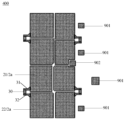
- FIG. 1A is an overall plan view of a display substrate provided by an embodiment of the present disclosure.
- the display substrate 10 includes a base substrate 1 and a display unit P disposed on the base substrate.
- it includes a plurality of display units P.
- the plurality of display units P are arranged in an array.
- Each display unit P includes a display area 11 and a non-emitting area 12.
- the display area 11 includes sub-pixels.
- the display unit P includes a plurality of sub-pixels arranged in an array.
- the array includes a first pixel row extending along the first direction D1.
- each display unit P includes adjacently arranged first sub-pixels P1 and second sub-pixels P2, and the second pixel row includes adjacently arranged third sub-pixels P3 and Four sub-pixels P4.
- 1A takes the display area 11 of each display unit P as an example including a first sub-pixel P1, a second sub-pixel P2, a third sub-pixel P3 and a fourth sub-pixel P4.
- each display The display area 11 of unit P also includes more than four or less than 4 sub-pixels.
- the first sub-pixel P1 may be a red sub-pixel (R) emitting red light
- the second sub-pixel P2 may be a green sub-pixel (G) emitting green light
- the second sub-pixel P2 may be a white sub-pixel emitting white light
- the fourth sub-pixel P4 may be a blue sub-pixel (B) that emits blue light.
- the emission colors of the first sub-pixel P1, the second sub-pixel P2, the second sub-pixel P2 and the fourth sub-pixel P4 are not limited to the above situation, and the embodiment of the present disclosure does not limit this.
- each sub-pixel may be a rectangle, a rhombus, a pentagon, or a hexagon.
- four sub-pixels may be arranged horizontally in parallel to form an RWBG pixel arrangement.
- the four sub-pixels may be arranged in a square, diamond or vertical arrangement, which is not limited in this disclosure.
- FIG. 2A is an equivalent circuit schematic diagram of the pixel circuit of four sub-pixels of one display unit P shown in FIG. 1A . 1A and 2A, each of the first sub-pixel P1, the second sub-pixel P2, the third sub-pixel P3 and the fourth sub-pixel P4 includes a pixel circuit, and the pixel circuit includes a driving transistor T1 and a light-emitting device 20; display Area 11 is a light-emitting area, used to display images; the non-light-emitting area is a non-light-emitting area, not used to display images, and can see through the environment on the non-display side.
- the driving transistor T1 is configured to control the magnitude of the driving current flowing through the light emitting device 20 and includes a gate electrode, a first electrode and a second electrode.
- the light emitting device 20 is configured to receive a driving current and be driven by the driving current to emit light.
- the display substrate is an organic light-emitting diode (OLED) display substrate, and the light-emitting device 20 is an OLED.
- OLED organic light-emitting diode
- FIG. 1B is a block diagram of a display substrate provided by at least one embodiment of the present disclosure.
- each of the first subpixel P1 , the second subpixel P2 , the third subpixel P3 and the fourth subpixel P4 includes a pixel circuit that drives the light emitting device 20 to emit light.
- the display substrate may further include a plurality of scanning lines and a plurality of data lines for providing scanning signals (control signals) and data signals for the plurality of sub-pixels, thereby driving the plurality of sub-pixels.
- the display substrate may further include power lines, detection lines, etc.
- the pixel circuit includes a driving sub-circuit for driving the light-emitting device 20 to emit light and a detection sub-circuit for detecting the electrical characteristics of the sub-pixel to achieve external compensation.
- the embodiments of the present disclosure do not limit the specific structure of the pixel circuit.
- FIG. 1B shows a schematic diagram of a 3T1C pixel circuit used in the display substrate.
- the pixel circuit may further include a compensation circuit, a reset circuit, etc.
- the pixel circuit may also have a 4T1C, 5T1C, 5T2C, 6T1C, 7T1C or 8T1C structure, for example.
- the embodiments of the present disclosure are not limited to this.
- each display unit P further includes a first scanning signal line G1, a second scanning signal line G2, a first power supply line vdd, a second power supply line line vss, four data signal lines D (in Figure 2A, the four data signal lines D are the first to fourth data signal lines D1 to D4 respectively, the first sub-pixel P1 is connected to the first data signal line D1, and the second The sub-pixel P2 is connected to the second data signal line D2, the third sub-pixel P3 is connected to the third data signal line D3, the fourth sub-pixel P4 is connected to the fourth data signal line D4), a detection signal line S and a detection signal line S respectively correspond to Four pixel circuits for four word pixels P1 ⁇ P2 ⁇ P3 ⁇ P4.
- first scanning signal line G1 and the second scanning signal line G2 extend along the first direction D1 and are arranged along the second direction D2.
- the first direction D1 intersects the second direction D2.
- the first direction intersects the second direction D2.
- Direction D2 is vertical.
- the first power supply line vdd, the data signal lines D1 ⁇ D2 ⁇ D3 ⁇ D4 and the detection signal line S may extend along the second direction D2 and be arranged along the first direction D1.
- four data signal lines D and one detection signal line S are provided between the first power line vdd and the second power line vss, and two of the four data signal lines D1 ⁇ D2 ⁇ D3 ⁇ D4 are D3 ⁇ D4.
- the other two data signal lines D1 ⁇ D2 among the four data signal lines D are located between the detection signal line S and the second power line vss.
- four sub-pixels are formed between the first power line vdd and the second power line vss by setting four data signal lines D1 ⁇ D2 ⁇ D3 ⁇ D4 and one detection signal line S.
- Four sub-pixels are also formed by arranging a first power supply line vdd, a second power supply line vss and four data signal lines D1 ⁇ D2 ⁇ D3 ⁇ D4.
- 2B-2D are signal timing diagrams of the driving method of the pixel circuit provided by the embodiment of the present disclosure.
- the pixel circuit of each of the first sub-pixel P1, the second sub-pixel P2, the third sub-pixel P3 and the fourth sub-pixel P4 includes a first transistor T1, a second transistor T2 , the third transistor T3 and the storage capacitor Cst.
- the first scanning signal line G1 is connected to the gate electrode of the second transistor T2 in each sub-pixel
- the second scanning signal line G2 is connected to the gate electrode of the third transistor T3 in each sub-pixel.
- the first electrode of the second transistor T2 is electrically connected to the first capacitor electrode of the storage capacitor Cst and the gate electrode of the first transistor T1, the data signal line is connected to the second electrode of the second transistor T2, and the second transistor
- the second electrode of T2 is configured to receive the data signal GT
- the second transistor T2 is a data transistor, and is configured to write the data signal DT into the gate of the first transistor T1 and the storage capacitor Cst in response to the first control signal G1
- the first electrode of a transistor T1 is electrically connected to the second capacitor electrode of the storage capacitor Cst, and is configured to be electrically connected to the first electrode of the light emitting element 20.
- the first power supply line VDD is connected to the second electrode of the first transistor T1.
- a second terminal of a transistor T1 is configured to receive a first power supply voltage V1 (for example, a high power supply voltage VDD).
- the first transistor T1 is a driving transistor and is configured to be at a voltage of a gate of the first transistor T1 .
- the current used to drive the light-emitting element is controlled under control;
- the first electrode of the third transistor T3 is electrically connected to the first electrode of the first transistor T1 and the second capacitor electrode of the storage capacitor Cst, and the detection signal line S is connected to the third transistor T3.
- the second pole is connected, and the second pole of the third transistor T3 is configured to be connected to the first detection line S to be connected to the external detection circuit 11 .
- the third transistor T3 is a detection transistor and is configured to detect in response to the second control signal G2
- the electrical characteristics of the sub-pixel are used to achieve external compensation; the electrical characteristics include, for example, the threshold voltage and/or carrier mobility of the first transistor T1, or the threshold voltage, driving current, etc. of the light-emitting element.
- the external detection circuit 11 is, for example, a conventional circuit including a digital-to-analog converter (DAC), an analog-to-digital converter (ADC), etc., which will not be described in detail in the embodiments of the present disclosure.
- the transistors used in the embodiments of the disclosure may be thin film transistors, field effect transistors, or other switching devices with the same characteristics.
- thin film transistors are used as examples for explanation.
- the source and drain of the transistor used here can be symmetrical in structure, so there can be no structural difference between the source and drain.
- one of the poles is directly described as the first pole and the other pole is the second pole.
- transistors can be divided into N-type and P-type transistors according to their characteristics.
- the turn-on voltage is a low-level voltage (for example, 0V, -5V, -10V or other suitable voltages), and the turn-off voltage is a high-level voltage (for example, 5V, 10V or other suitable voltages) );
- the turn-on voltage is a high-level voltage (for example, 5V, 10V or other suitable voltages), and the turn-off voltage is a low-level voltage (for example, 0V, -5V, -10V or other suitable voltages) voltage).
- the transistor in FIG. 1B is an N-type transistor as an example, but this is not intended to limit the present disclosure.
- Figure 2A shows the working principle of the pixel circuit during the display process.
- Figure 2B shows the signal timing diagram of the pixel circuit during the display process.
- Figures 2C and 2D show The signal timing diagram of the pixel circuit during the detection process is shown.
- the display process of each frame image includes data writing and resetting stage 1 and lighting stage 2.
- Figure 2B shows the timing waveforms of each signal in each stage.
- a working process of the 3T1C pixel circuit includes: in the data writing and reset phase 1, the first control signal G1 and the second control signal G2 are both turn-on signals, the second transistor T2 and the third transistor T3 are turned on, and the data signal DT is transmitted to the gate of the first transistor T1 through the second transistor T2, the first switch K1 is closed, and the analog-to-digital converter transmits the signal to the first electrode of the light-emitting element (such as the anode of the OLED) through the first detection line 130 and the third transistor T3.
- the first electrode of the light-emitting element such as the anode of the OLED
- the first transistor T1 When the reset signal is written, the first transistor T1 is turned on and generates a driving current to charge the first electrode of the light-emitting element to the operating voltage; in the light-emitting phase 2, the first control signal G1 and the second control signal G2 are both off signals. Due to the storage Due to the bootstrap effect of the capacitor Cst, the voltage across the storage capacitor Cst remains unchanged. The first transistor T1 works in a saturated state with a constant current and drives the light-emitting element to emit light.
- FIG. 2C shows a signal timing diagram of the pixel circuit when detecting the threshold voltage.
- a working process of the 3T1C pixel circuit includes: the first control signal G1 and the second control signal G2 are both turn-on signals, the second transistor T2 and the third transistor T3 are turned on, and the data signal DT is transmitted to the third transistor through the second transistor T2.
- the node S is charged until the first transistor is turned off, and the digital-to-analog converter samples the voltage on the first detection line 130 to obtain the threshold voltage of the first transistor T1.
- This process may be performed, for example, when the display device is turned off.
- FIG. 2D shows a signal timing diagram of the pixel circuit when detecting the threshold voltage.
- a working process of the 3T1C pixel circuit includes: in the first stage, the first control signal G1 and the second control signal G2 are both turn-on signals, the second transistor T2 and the third transistor T3 are turned on, and the data signal DT passes through the second The transistor T2 transmits to the gate of the first transistor T1; the first switch K1 is closed, and the analog-to-digital converter writes a reset signal to the first electrode (node S) of the light-emitting element through the first detection line 130 and the third transistor T3; in In the second stage, the first control signal G1 is a turn-off signal, the second control signal G1 is a turn-on signal, the second transistor T2 is turned off, the third transistor T3 is turned on, and the first switch K1 and the second switch K2 are turned off.
- the first transistor T1 Floating the first detection line 130; due to the bootstrap effect of the storage capacitor Cst, the voltage across the storage capacitor Cst remains unchanged, the first transistor T1 works in a saturated state with unchanged current and drives the light-emitting element to emit light, and then digital-to-analog conversion
- the device samples the voltage on the first detection line 130 and combines it with the magnitude of the light-emitting current to calculate the carrier mobility in the first transistor T1. For example, this process can be performed during the blanking phase between display phases.
- the electrical characteristics of the first transistor T1 can be obtained and the corresponding compensation algorithm can be implemented.
- the display substrate 10 may further include a data driving circuit 03 and a scan driving circuit 04 .
- the data driving circuit 03 is configured to emit a data signal, such as the above-mentioned data signal DT, as needed (such as an image signal input to the display device); the pixel circuit of each sub-pixel is also configured to receive the data signal and apply the data signal to the third The gate of a transistor.
- the scan driving circuit 04 is configured to output various scanning signals, including, for example, the above-mentioned first control signal G1 and the second control signal G2, which is, for example, an integrated circuit chip (IC) or a gate driving circuit (GOA) directly prepared on the display substrate. ).
- the display substrate 10 further includes a control circuit 02 .
- the control circuit 02 is configured to control the data driving circuit 03 to apply the data signal, and to control the gate driving circuit 03 to apply the scanning signal.
- An example of the control circuit 02 is a timing control circuit (T-con).
- the control circuit 02 can be in various forms, for example, including a processor 021 and a memory 022.
- the memory 022 includes executable code, and the processor 021 runs the executable code to perform the above detection method.
- the processor 021 may be a central processing unit (CPU) or other form of processing device with data processing capabilities and/or instruction execution capabilities, and may include, for example, a microprocessor, a programmable logic controller (PLC), etc.
- CPU central processing unit
- PLC programmable logic controller
- memory 022 may include one or more computer program products, which may include various forms of computer-readable storage media, such as volatile memory and/or non-volatile memory.
- Volatile memory may include, for example, random access memory (RAM) and/or cache memory (cache), etc.
- Non-volatile memory may include, for example, read-only memory (ROM), hard disk, flash memory, etc.
- One or more computer program instructions may be stored on the computer-readable storage medium, and the processor 021 may execute the functions desired by the program instructions.
- Various application programs and various data can also be stored in the computer-readable storage medium, such as the electrical characteristic parameters obtained in the above detection method.
- FIG. 3A is a schematic plan view of a display unit P of the display substrate 10 provided by at least one embodiment of the present disclosure
- FIG. 3B is a schematic view of the third sub-pixel P3 in FIG. 3A
- FIG. 3C is a partial L including a connection structure in FIG. 3B An enlarged view
- Figure 4A is a schematic cross-sectional view along line AA' in Figure 3B.
- the light emitting device 20 includes a first electrode 2 including a first portion 21 and a second portion 22 spaced apart from each other.
- the display unit P also includes: a connection structure 3 and a first transfer electrode 4 .
- connection structure 3 connects the first part 21 of the first electrode 2 and the second part 22 of the first electrode 2 and includes a connection part 30 located in the non-light-emitting area 12; the first transfer electrode 4 and the first electrode T1s of the driving transistor T1 Connected to and including a portion located in the non-luminescent region 12 , the connecting portion 30 is electrically connected in the non-luminescent region 12 to a portion of the first transfer electrode 4 located in the non-luminescent region 12 .
- multiple parts of the first electrode 2 such as the first part 21 and the second part 22, are connected to the first electrode T1s of the driving transistor T1 through the connection part 30 and the first transfer electrode 4.
- the opening area of a sub-pixel includes a first sub-opening 601 and a second sub-opening 602 (as shown in Figure 5K).
- the first sub-opening 601 and the second sub-opening 602 is the area corresponding to the first part 21 of the first electrode 2 and the second part 22 of the first electrode 2 respectively.
- the first part 21 of an electrode 2 covers the first sub-opening 601, and the second part 22 of the first electrode 2
- the second sub-opening 602 is covered.
- the first portion 21 of the first electrode 2 and the second portion 22 of the first electrode 2 are electrically connected to the connection portion 30 located in the non-luminous area 12 in the non-luminous area 12, and then are located in the display area through the first transfer electrode 4.
- the part 11 is connected to the first electrode T1s of the driving transistor T1.
- the first transfer electrode 4 is located in the display.
- the portion of the region 11 is connected to the first electrode T1s of the driving transistor T1 so that a via hole for connecting the connection portion 30 to the first transfer electrode 4 is made in the non-light-emitting region 12 .
- the embodiment of the present disclosure is The position of the non-light-emitting area 12 corresponding to the connection part 30 makes the alignment process of making via holes for connecting the connection part 30 and the first transfer electrode 4 easier, and the yield rate can be significantly improved.
- the longitudinal portion vdd1 of the first power line vdd and the second power line vss are spaced apart in the first direction D1 and are respectively located in the display area 11 in the first direction D1
- the area between the edges of the longitudinal portion vdd1 of the first power line vdd is the display area 11 .
- the light-emitting element is an organic light-emitting diode, including a first electrode 2 , a second electrode 24 , and a light-emitting layer 23 located between the first electrode 2 and the second electrode 24 .
- the first electrode is a material with a high work function to serve as an anode, such as an ITO/Ag/ITO stacked structure, or an ITO/Al/ITO stacked structure (sandwich structure), or ITO/(Al+Ag) /ITO laminated structure (sandwich structure).
- the first electrode is not limited to the above-mentioned sandwich structure, and the material of the first electrode is not limited to the above-mentioned types.
- the second electrode 24 is a material with a low work function to serve as a cathode, such as a semi-transmissive metal or metal alloy material, such as an Ag/Mg alloy material.
- the light-emitting element has a top-emission structure, the first electrode 2 is reflective and the second electrode 122 is transmissive or semi-transmissive.
- the first transfer electrode 4 includes a first transfer portion 41, which is located in the display area 11 and connected to the first pole of the driving transistor T1;
- the portion of the connecting electrode 4 located in the non-light-emitting area 12 includes a second connecting portion 42, the second connecting portion 42 is connected to the first connecting portion 41, the connecting portion 30 and the second connecting portion 42 are arranged in different layers, and,
- the connection part 30 is connected to the second adapter part 42 in the non-light-emitting area 12 through the first via hole V0.
- the display unit P further includes a second transfer electrode 5 .
- the second transfer electrode 5 is located in the non-light-emitting area 12 and is located between the connection portion 30 and the second transfer electrode 5 in a direction perpendicular to the base substrate 1 . between the transfer portion 42 and the orthographic projection of the second transfer electrode 5 on the base substrate 1 and the orthographic projection of the connection portion 30 on the base substrate 1 and the orthographic projection of the second transfer portion 5 on the base substrate 1 .
- the orthographic projections all at least partially overlap; the connection part 30 is connected to the second transfer part 42 through the second transfer electrode 5 and is connected in segments, thereby reducing the possibility that the connection part 30 is directly connected to the second transfer part 42 through a via hole. Hole depth improves the manufacturing yield of display substrates.
- the display substrate 10 further includes a first insulating layer 101 , a second insulating layer 102 located on a side of the first insulating layer 101 away from the substrate 1 , and a second insulating layer 102 located on a side of the second insulating layer 102 away from the substrate 1 .
- the third insulating layer 103 on one side of the base substrate 1, the fourth insulating layer 104 located on the second transfer electrode 5 away from the third insulating layer 103 in the direction perpendicular to the base substrate 1, and the interlayer insulating layer 105 is vertical It is located on the side of the fourth insulating layer 104 away from the third insulating layer 103 in the direction of the base substrate 1 .
- the first via V0 includes a first sub-via V01 penetrating the first insulating layer 101 and the third insulating layer 103.
- the second transfer electrode 5 is connected to the second transfer part 42 through the first sub-via V01; display substrate 10 also includes that the first via V0 also includes a second sub-via V02 penetrating the fourth insulating layer 104, and the connection part 30 is connected to the second transfer electrode 5 through the second sub-via V02, thereby realizing the connection part 30 It is connected to the second adapter part 42 through multi-level via holes.
- the first adapter part 41 and the second adapter part 42 are a continuous integrally formed structure.
- the material of the first transfer electrode 4 is a metal material, such as copper, aluminum, chromium, copper alloy, aluminum alloy, chromium alloy, manganese alloy, etc., but is not limited to the types listed above.
- the display unit P further includes an interlayer insulating layer 105.
- the interlayer insulating layer 105 is located in the display area 11 and not in the non-emitting area 12. In a direction perpendicular to the base substrate 1, the interlayer insulating layer 105 is located on the first electrode. 2 and the second transfer electrode 5.
- the first electrode 2 is electrically connected to the first electrode T1s of the driving transistor T1 through the opening O1 penetrating the interlayer insulating layer 5 in a direction perpendicular to the base substrate 1 .
- the opening O1 is connected to the second sub-via hole V02, and the first electrode 2 enters the second sub-via hole V02 through the opening O1 penetrating the interlayer insulating layer 5 and is connected to the second transfer electrode 5.
- the orthographic projection of the first via hole on the base substrate 1 is located within the orthographic projection of the opening O1 on the base substrate 1 , that is, the second sub-via hole V02 and the first sub-via hole V01 are on the base substrate 1
- the orthographic projection of is located within the orthographic projection of the opening O1 on the base substrate 1 .
- the first electrode 2 can be electrically connected to the first electrode T1s of the driving transistor T1 through the larger opening O1 of the interlayer insulating layer 105 in the non-light-emitting area, thereby facilitating the realization of the connection portion 30 and the second connection in the non-light-emitting area.
- the connection of the electrode 5 and the creation of a larger opening O1 in the non-emitting area have lower requirements on the manufacturing process and are easy to implement.
- the accuracy of making the opening O1 is high and has little impact on other surrounding structures.
- the insulation layer in the display area 11 is avoided.
- the problem of low through-hole production yield and great impact on surrounding structures is caused by the space limitation of mid-hole drilling.
- the interlayer insulating layer 105 is located in the display area 11 and is not located in the non-emitting area 12A. That is, the interlayer insulating layer 105 does not include a portion located in the non-emitting area 12A.
- the portion of the material layer used to form the interlayer insulating layer 105 located in the non-emitting region 12A is completely removed through a patterning process, thereby forming an opening O1 in the non-emitting region in the same layer as the interlayer insulating layer 105.
- the orthographic projection of the opening O1 on the base substrate 1 is located in the non-light-emitting area 12A, and the area of the orthographic projection of the opening O1 on the base substrate 1 is equal to the area of the non-light-emitting area 12A.
- the production of the interlayer insulating layer 105 can be further reduced compared to the solution of making via holes in the non-display area 12A for passing the first electrode 2 Difficulty, improve the production yield of display substrates.
- the area of the orthographic projection of the opening O1 on the base substrate 1 is larger than the area of the orthogonal projection of a sub-pixel adjacent to the opening O1 on the base substrate 1 .
- the maximum width W1 of the opening O1 is greater than the maximum width W2 of a sub-pixel.
- a sub-pixel adjacent to the opening O1 Take P3 as an example.
- the orthographic projection of the opening O1 on the base substrate 1 is located in the non-emitting area 12A, and the area of the orthographic projection of the opening O1 on the base substrate 1 is smaller than the non-emitting area. 12A area. That is, in the process of making the interlayer insulating layer 105, part of the portion of the material layer used to form the interlayer insulating layer 105 located in the non-emitting region 12A is removed through a patterning process, thereby forming the opening O1, which is A larger via hole passes through the interlayer insulating layer 105 , and the edge of the opening O1 is at least partially surrounded by the material of the interlayer insulating layer 105 .
- Other features and corresponding technical effects of the embodiment shown in Figure 4D are the same as those in Figure 4A. Please refer to the description of Figure 4A.
- the interlayer insulating layer 105 has a fault at the junction of the display area 11 and the non-emitting area 12 , that is, there is a step structure 001 on the edge of the interlayer insulating layer 105 close to the non-emitting area 12 , and the first electrode 2
- the step structure 001 is covered to extend across the step structure 001 to the non-light-emitting area 12 .
- the interlayer insulating layer 105 is no longer provided on the side of the step structure 001 close to the non-light-emitting area 12 , so that the connection portion 30 can be located on the step structure 001 Compared with the solution in which the interlayer insulating layer 105 is located in the display area 11 and the non-emitting area 12, this embodiment can avoid making a through-layer in the interlayer insulating layer 105.
- the via hole of the insulating layer 105 used to connect the connecting portion 30 to the second transfer electrode 5 simplifies the manufacturing process of the display substrate and is of great significance to improving the yield of the display substrate; because the interlayer insulating layer 105 is perpendicular to The thickness in the direction of the base substrate 1 is relatively large.
- the thickness of the interlayer insulating layer 105 in the direction perpendicular to the base substrate 1 is greater than 6000 Angstroms to satisfy its function of insulation and serving as a flat layer. If the interlayer insulation is made through
- the via holes of the layer 105 for connecting the connection portion 30 to the second transfer electrode 5 have different sizes in the direction parallel to the base substrate from the via holes used for other purposes in the interlayer insulating layer 105. For example, the size of the via hole in the direction parallel to the base substrate is required to be larger. Therefore, when multiple via holes penetrating the interlayer insulating layer 105 are produced through the same patterning process, it is difficult to meet these different sizes at the same time.
- the above solution of the embodiment of the present disclosure can avoid making a via hole penetrating the interlayer insulating layer 105 for connecting the connecting portion 30 to the second transfer electrode 5 in the interlayer insulating layer 105 , thereby avoiding the above problem.
- the material of the interlayer insulating layer 105 is an organic insulating material.
- the organic insulating material includes resin material, acrylic material, etc., for example, it can be polyimide (PI), acrylate, epoxy resin, polymethylmethacrylate. ester (PMMA), etc., but are not limited to the types listed above.
- the interlayer insulating layer 105 is a planarization layer.
- the first insulating layer 101, the second insulating layer 102, the third insulating layer 103, and the fourth insulating layer 104 are, for example, inorganic insulating layers, such as silicon oxide, silicon nitride, silicon oxynitride, etc., silicon oxides, etc. Nitride or silicon oxynitride, or aluminum oxide, titanium nitride, etc. include metal oxynitride insulating materials.
- the display substrate 10 further includes first signal lines G1/G2 and second signal lines D1 to D4 provided on the base substrate 1 .
- the first signal line G1/G2 transmits the scanning signal; for example, the first signal line includes a first sub-scanning signal line G1 and a second sub-scanning signal line G2; the first sub-scanning signal line G1 transmits the first scanning signal, and the second sub-scanning signal line G2
- the signal line G2 transmits the second scanning signal; for example, the first scanning signal and the second scanning signal may be progressive scanning signals, for example, the first scanning signal and the second scanning signal are the same scanning signal, please refer to the above-mentioned Figure 2B; or, In other embodiments, the first scanning signal and the second scanning signal are different signals.
- the second signal lines D1 to D4 transmit the data signal DT;
- the first signal lines extend as a whole along the first direction D1, and the second signal lines D1 to D4 as a whole extend along the second direction D2 that intersects the first direction D1;
- the sub-pixel further includes a data writing transistor T2 configured to transmit the data signal to the driving transistor T1 under the control of the first scan signal.
- first direction D1 includes extending generally along the first direction D1, and at least it suffices that it extends entirely along the first direction D1.
- first signal line extending overall along the first direction D1 may have a certain curved portion, or, in some examples, the edge of the strip extending overall along the second direction D2 It may not be a smooth line, for example, its edge may have burrs or jagged edges. In short, it is sufficient as long as the overall extension trend is along the first direction D1.
- extending as a whole along the second direction D2 This is also true for any reference in this disclosure to extending in a certain direction as a whole.
- connection structure 3 includes at least two extension parts, and the at least two extension parts include: a first extension part 31 and a second extension part 32 .
- the first extension part 31 has a first end and a second end opposite to the first end, and extends from the display area 11 to the non-light emitting area 12 .
- the first end of the first extension part 31 is connected to the first part 21 of the first electrode 2 connected, the second end of the first extension part 31 is located in the non-light-emitting area 12;
- the second extension part 32 has a first end and a second end opposite to the first end, and extends from the display area 11 to the non-light-emitting area 12,
- the first end of the two extension parts 32 is connected to the second part 22 of the first electrode 2, and the second end of the second extension part 32 is located in the non-light-emitting area 12;
- the connection part 30 is connected to the second end of the first extension part 31 and the second end of the first extension part 31.
- the second ends of the two extension parts 32 are connected.
- the connecting part 30 is connected to the first part 21 of the first electrode 2 and the second part 22 of the first electrode 2 respectively through at least one channel, that is, the first extending part 31 and the second extending part 32.
- a sub-pixel such as the When a dark spot or other display failure occurs in one of the opening area of the three sub-pixels P3 corresponding to the first part 21 of the first electrode 2 and the area corresponding to the second part 22 of the first electrode 2
- the area can be One of the first extension part 31 and the second extension part 32 corresponding to the area where dark spots or other display defects occur is cut off, so that the area where dark spots or other display defects occur is not displayed, and the first extension part 31 and the second extension part 32
- the two extending portions 32 are in the form of strips extending along the first direction D1, which are easy to cut, thereby facilitating the repair of sub-pixels and improving the display quality.
- the second end of the first extension part 31 has a first cutable part 310
- the second end of the second extension part 32 has a second cuttable part 320;
- the maximum width W SP of the interval between the first portion 21 of the first electrode 2 and the second portion 22 of the first electrode 2 in the second direction D2 is smaller than the maximum width W SP of the connecting portion 30 in the second direction D2
- the maximum width W C on the second direction D2 is to ensure that the connecting portion 30 has sufficient width to connect the first portion 21 of the first electrode 2 and the second portion 22 of the first electrode 2 , and so that the first electrode 2
- the distance between the first part 21 and the second part 22 of the first electrode 2 should not be too large to occupy too much space, so as to achieve a high PPI display panel at the same time.
- the first part 21 of the first electrode 2 , the second part 22 of the first electrode 2 , the first extension part 31 , the second extension part 32 and the connecting part 30 are a continuous one-piece structure to simplify the structure of the display substrate.
- the above-mentioned continuous one-piece structure can be formed by performing the same patterning process on the same material layer, which simplifies the manufacturing process of the display substrate.
- each sub-pixel further includes a first power line vdd.
- the first power line vdd is connected to the first voltage terminal VDD and is configured to provide a first power voltage to the sub-pixel.
- the first power line vdd is connected to the first power line vdd.
- the first pole of the driving transistor T1 is arranged in the same layer and includes a vertical portion vdd1.
- the vertical portion vdd1 extends overall along the second direction D2 and is connected to its adjacent sub-pixels; for example, the first power line vdd also includes The transverse portion vdd2 is electrically connected to the longitudinal portion and extends overall along the first direction D1 to be connected to each sub-pixel of the display unit, thereby providing the first power supply voltage to each sub-pixel of the display unit.
- the horizontal portion vdd2 in Figure 3B is connected to the third sub-pixel P3 and the fourth sub-pixel P4, and Figure 3A also includes another bar connected to the longitudinal portion vdd2 and connected to the first sub-pixel P1 and the second sub-pixel P2.
- the horizontal part vdd2 is provided to realize supplying the first power supply voltage from the vertical part vdd1 to each sub-pixel of the display unit.
- the first extension part 31 and the second extension part 32 extend across the first power line vdd and the second signal line to the non-light-emitting area 12 to connect with the connection part located in the non-light-emitting area 12 .
- the non-luminescent area 12 and the display area 11 are arranged in the second direction D2
- the first part 21 of the first electrode 2 and the second part 22 of the first electrode 2 are arranged in the second direction D2
- the first Both the extending portion 31 and the second extending portion 32 extend along the first direction D1 as a whole.
- Such an arrangement can coordinate the positions of the first part 21 of the first electrode 2 and the second part 22 of the first electrode 2 and the non-emitting areas corresponding to the sub-pixels in which they are located, thereby facilitating the separation between the first part 21 and the second part 22 of the first electrode 2.
- the second part 22 of the first electrode 2 respectively leads the first extension part 31 and the second extension part 32 to the non-light-emitting area 12, so as to facilitate the connection between the connection part 30 located in the non-light-emitting area 12 and the first part 21 of the first electrode 2.
- the second part 22 of the first electrode 2 is connected.
- the non-light-emitting area 12 includes a first non-light-emitting area 12A located on a first side of the display area 11 in the first direction D1 and a second non-light-emitting area 12B located on A second side of the display area 11 opposite to its first side in the first direction D1; the first sub-pixel P1 and the third sub-pixel P3 are adjacent to the first non-light-emitting area 12A, the second sub-pixel P2 and the fourth sub-pixel
- the pixel P4 is adjacent to the first non-emitting area 12A; a connection structure 3 is provided corresponding to each of the plurality of sub-pixels, and the connection structure 3 connects the first part 21 of the first electrode 2 of the adjacent sub-pixel and the first electrode 2
- the second part 22; the connection part 30 corresponding to the connection structure 3 of the first sub-pixel P1 and the connection part 30 corresponding to the connection structure 3 of the third sub-pixel P3 are located in the first non-emitting area 12A; corresponding to the
- the first signal lines G1/G2 that provide scanning signals to the first sub-pixel P1, the second sub-pixel P2, the third sub-pixel P3 and the fourth sub-pixel P4 are located in the first pixel row and the first pixel row.
- the planar patterns of the first sub-pixel P1 and the second sub-pixel P2 are symmetrical with respect to the symmetry axis extending along the second direction D2
- the planar pattern of the third sub-pixel P3 is symmetrical with the symmetry axis of the fourth sub-pixel P4
- the planar pattern of the first non-light-emitting area 12A and the second non-light-emitting area 12B is symmetrical with respect to the symmetry axis to rationally utilize space and improve the uniformity of the display substrate, thereby improving the uniformity of display in the display area and reducing the difficulty of manufacturing the display substrate.
- the display unit P further includes a pixel defining layer 6
- the pixel defining layer 6 includes: a first part 61 and a second part 62 .
- the first portion 61 is located between the first electrodes 2 of adjacent sub-pixels to define an opening area 60 of the sub-pixel, and the light-emitting layer 23 of the light-emitting device 20 is at least located in the opening area 60 .
- the second portion 62 is located between the first portion 21 of the first electrode 2 and the second portion 22 of the first electrode 2 to separate the first portion 21 of the first electrode 2 from the second portion 22 of the first electrode 2 .
- the orthographic projection of the connecting portion 30 on the base substrate 1 is located within the orthographic projection of the first portion 61 of the pixel defining layer 6 on the base substrate 1 to avoid the connecting portion 30 and the pixel defining layer 6
- Each of the first parts 61 occupies an independent space to save space, and the first part 61 of the pixel definition layer 6 is used to protect the connection part 30 .
- the light-emitting element of the display substrate 10 may adopt a top-emission structure.
- each sub-pixel taking the third sub-pixel P3 as an example, also includes a first capacitor C1; the first capacitor C1 includes a first plate Ca and a second plate Cb; the first plate Ca It is electrically connected to the gate electrode T1g of the driving transistor T1 and is arranged on the same layer as the gate electrode of the driving transistor T1.
- the first plate Ca is an integrated structure that is continuous with the gate electrode T1g of the driving transistor T1; the second plate Cb is on the substrate.
- the orthographic projection on the substrate 1 at least partially overlaps the orthographic projection of the first electrode plate Ca on the base substrate 1 .
- the sub-pixel taking the third sub-pixel P3 as an example, also includes a second capacitor C2.
- the second capacitor C2 includes a first plate Ca and a third plate Cc;
- the third plate Cc includes The overlapping portion and the non-overlapping portion, the orthographic projection of the overlapping portion on the base substrate 1 overlaps with the orthographic projection of the first electrode plate Ca on the base substrate 1, and the orthographic projection of the non-overlapping portion on the base substrate 1 overlaps with the orthographic projection of the first electrode plate Ca on the base substrate 1
- the orthographic projection of the electrode plate Ca on the base substrate 1 does not overlap and at least partially overlaps the orthographic projection of the second electrode plate Cb on the base substrate 1 .
- Figure 4B is a schematic cross-sectional view along line BB' and line CC' in Figure 3B. As shown in Figure 4B, the non-overlapping portion is connected to the second plate Cb through the second via V2, and the third plate Cc is multiplexed as the first adapter portion 41 , that is, the first adapter portion 41 and the second plate Cb are connected through the second via hole V2 to simplify the structure and manufacturing process of the display substrate 10 .
- the second plate Cb and the first electrode T1s of the driving transistor T1 are arranged on the same layer.
- the second plate Cb and the first electrode T1s of the driving transistor T1 have a continuous integrated structure, so as to realize the third
- the diode plate Cb is electrically connected to the first pole T1s of the driving transistor T1, thereby realizing the electrical connection between the first switching part 41 and the first pole T1s of the driving transistor T1.
- the integrated structure in which the third plate Cc is multiplexed as the first connecting portion 41 and the second plate Cb and the first electrode T1s of the driving transistor T1 greatly simplifies the structure and manufacturing process of the display substrate 10 .
- the first electrode T1s of the driving transistor T1 is connected to the active layer T1a of the driving transistor T1 through a plurality of via holes to reduce the contact resistance; for example, the plurality of via holes are spaced apart from each other along the second direction D2 arrangement; for example, the first electrode T1s of the driving transistor T1 is connected to the active layer T1a of the driving transistor T1 through three vias: via V91, via V92 and via V93.
- the via V91, via V92 and via V93 are all penetrating the second insulating layer 102 and the third insulating layer 103 .
- the number of the multiple via holes is not limited to three, and can be designed as needed.
- Figure 5A is a schematic plan view of the first conductive layer of the display unit shown in Figure 3A;
- Figure 5B is a schematic plan view of the first insulating layer of the display unit shown in Figure 3A;
- Figure 5C is a semiconductor of the display unit shown in Figure 3A
- Figure 5D is a schematic plan view of the second conductive layer of the display unit shown in Figure 3A;
- Figure 5E is a schematic plan view of the third insulating layer of the display unit shown in Figure 3A;
- Figure 5F is a schematic plan view of the third insulating layer of the display unit shown in Figure 3A
- Figure 5G is a schematic plan view of the third conductive layer of the display unit shown in Figure 3A;
- Figure 5H is a schematic plan view of the fifth insulating layer of the display unit shown in Figure 3A;
- the display substrate 10 includes a first conductive layer 100 and a first insulating layer 101 sequentially stacked on the base substrate 1 in a direction from close to the base substrate 1 to away from the base substrate 1 .
- the fifth insulating layer 105 is also the above-mentioned interlayer insulating layer 105.
- the materials of the semiconductor layer 600 include but are not limited to silicon-based materials (amorphous silicon a-Si, polycrystalline silicon p-Si, etc.), metal oxide semiconductors (IGZO, ZnO, AZO, IZTO, etc.) and organic materials (hexathiophene, Polythiophene, etc.).
- silicon-based materials amorphous silicon a-Si, polycrystalline silicon p-Si, etc.
- metal oxide semiconductors IGZO, ZnO, AZO, IZTO, etc.
- organic materials hexathiophene, Polythiophene, etc.
- the first conductive layer 100 includes a first transfer part 41, a second transfer part 42 and a third plate Cc;
- the semiconductor layer 600 includes the active layer T1a of the driving transistor T1, the data The active layer T2a of the transistor T2 and the active layer T3a of the detection transistor T3;
- the second conductive layer 200 includes the first sub-scanning signal line G1 and the second sub-scanning signal line G2, the gate electrode T1g of the driving transistor T1, and the data transistor T2
- the gate T2g and the gate T3g of the detection transistor T3, the first plate Ca, the lateral portion vdd2 of the first power line vdd and the auxiliary power line vdd3, the auxiliary power line vdd3 corresponds to the vertical portion vdd1 of the first power line vdd Extends along the second direction D2, and is electrically connected to the vertical portion vdd1 of the first power line vdd through a plurality of vias V4 penetr
- the auxiliary power line vdd3 is electrically connected to the lateral part vdd2, thereby realizing the electrical connection between the lateral part vdd2 and the vertical part vdd1.
- the auxiliary power line vdd3 and the lateral portion vdd2 are arranged on the same layer, and both are located on the second conductive layer 200 .
- the auxiliary power line vdd3 and the horizontal part vdd2 have a continuous integrated structure.
- the third conductive layer 300 includes a first pole T1s and a second pole T1d of the driving transistor T1, a first pole T2s and a second pole T2d of the data transistor T2, a first pole T3s and a second pole T3d of the detection transistor T3, and a data line. D1 ⁇ D2 ⁇ D3 ⁇ D4, the detection signal line S, and the vertical part vdd1 of the first power line vdd. It can be seen from FIG. 4A and FIG. 5H that the above-mentioned interlayer insulating layer 105 is only provided in the display area 11 , and there is no interlayer insulating layer 105 in the non-light-emitting area 12 .
- the first portion 21 of the first electrode 2 and the second portion 22 of the first electrode 2 are connected to the first electrode T1s of the driving transistor T1, and are respectively included in the direction perpendicular to the base substrate 1
- the first sub-electrode layer 2a, the second sub-electrode layer 2b and the third sub-electrode layer 2c are sequentially stacked on the substrate in a direction from close to the base substrate 1 to away from the base substrate 1.
- the fourth conductive layer 400 includes a connecting portion 30 , a first extending portion 31 , a second extending portion 32 , a first sub-electrode layer 2 a of the first portion 21 , and a first sub-electrode layer 2 a of the second portion 22 .
- the fifth conductive layer 500 includes the third sub-electrode layer 2c of the first part 21 and the third sub-electrode layer 2c of the second part 22.
- the display substrate 10 further includes a sixth conductive layer.
- the sixth conductive layer is located between the fourth conductive layer 400 and the fifth conductive layer 500 in a direction perpendicular to the substrate substrate 1 .
- the sixth conductive layer includes the first portion 21 The second sub-electrode layer 2b and the second sub-electrode layer 2b of the second portion 22.
- Figure 4C is a schematic cross-sectional view along line D-D' in Figure 3A.
- the first conductive layer 100 further includes an intermediate connection portion 43 .
- the intermediate connection portion 43 is located in the boundary area between the first pixel row and the second pixel row.
- the second electrode T3d of the detection transistor T3 is connected to the active layer T3a of the detection transistor T3 through the middle via V33 penetrating the third insulating layer 103, and through the second connection via V33 penetrating the third insulating layer 103 and the first insulating layer 101.
- the hole V32 is connected to the middle connection part 43; and the detection signal line S is connected to the middle connection part 43 through the first connection via V31 penetrating the third insulating layer 103 and the first insulating layer 101, thereby realizing the detection signal line S and the detection
- the second terminal T3d of the transistor T3 is connected.
- the second electrode T3d' of the detection transistor of the fourth sub-pixel P4 is connected to the active layer T3a' of the detection transistor of the fourth sub-pixel P4 through the via V35 penetrating the third insulating layer 103, and through the third insulating layer 103
- the via V34 of the layer 103 and the first insulating layer 101 is connected to the middle connection portion 43, thereby realizing the passage of the second pole T3d of the detection transistor of the third sub-pixel P3 and the second pole T3d' of the detection transistor of the fourth sub-pixel P4.
- the same intermediate connection part 43 is connected to the same detection signal line S, thereby simplifying the structure and manufacturing process of the display substrate 10 .
- the detection of the second pole T3d of the detection transistor T3 of the first sub-pixel P1 (ie, the upper sub-pixel below) and the third sub-pixel P3 (ie, the lower sub-pixel below) The second electrode T3d of the transistor T3 forms a continuous integrated electrode, and the active layer T3a of the detection transistor T3 of the first sub-pixel P1 and the active layer T3a of the detection transistor T3 of the third sub-pixel P3 are integrated with the active layer IAL.
- the integrated electrode is electrically connected to the integrated active layer IAL through the middle via hole V33.
- the third electrode plate Cc is located on the side of the first electrode plate Ca close to the base substrate 1 .
- the display substrate 10 further includes a light-shielding layer 7 , which is located on a side of the semiconductor layer 200 close to the base substrate 1 ; the active pattern of the driving transistor T1 (ie, the active layer T1a or trench The orthographic projection of the channel area) on the base substrate 1 is located within the orthographic projection of the light-shielding layer 7 on the base substrate 1, so that the light-shielding layer 7 is used to block the active pattern from the driving transistor T1 away from the base substrate 1.
- the top light on the side prevents the top light from irradiating the channel area of the driving transistor T1, thereby preventing the light from degrading the performance of the driving transistor T1.
- the light-emitting device 20 is a top-emitting type, and the light emitted by the light-emitting layer 23 is emitted from the side of the light-emitting device 20 away from the substrate 1 .
- the light-emitting device 20 can also be a bottom-emitting type, and the light emitted by the light-emitting layer 23 passes through the substrate.
- the bottom substrate 1 is emitted.
- the light-shielding layer 7 is reused as the first adapter portion 41 , that is, the two have the same structure, so as to simplify the structure and manufacturing process of the display substrate 10 .
- At least one embodiment of the present disclosure also provides an operating method for a display substrate, which is applicable to any display substrate 10 provided by the embodiment of the present disclosure.
- the operating method includes: connecting the connection structure 3 of the display substrate 10 to Part of the non-luminous area is cut off to disconnect the connection structure 3 from one of the first part 21 of the first electrode 2 and the second part 22 of the first electrode 2.
- the "disconnection" here refers to the connection structure 3 and one of the first part 21 and the second part 22 of the first electrode 2.
- One of the first part 21 and the second part 22 is no longer electrically connected, for example, the connection structure 3 is connected to one of the first part 21 of the first electrode 2 and the second part 22 of the first electrode 2 .
- connection portion 30 of the connection structure 3 located in the non-light-emitting area 12 is disconnected.
- the opening area corresponds to the area of the first part 21 of the first electrode 2 and the area corresponding to the second part 22 of the first electrode 2
- a dark spot or other display failure occurs in the area corresponding to the first part 21 of the first electrode 2
- the first part 21 of the first electrode 2 can be disconnected from the connection structure 3, thereby Areas with poor display such as dark spots will not be displayed to achieve sub-pixel repair and improve display quality.
- the operating method of the display substrate includes removing one of the first cutable portion 310 and the second cutable portion 320 .
- One is cut off to disconnect one of the first part 21 of the first electrode 2 and the second part 22 of the first electrode 2 from the connection part 30 .
- other conductive layers will not be damaged during cutting of the first cutable portion 310 or the second cutable portion 320, thereby facilitating cutting, achieving repair of sub-pixels, and improving display quality.
- laser irradiation can be used to cut the first cutable portion 310 or the second cutable portion 320 to form a fracture (not shown).
- the fracture separates the first cutable portion 310 or the second cutable portion 320 . It is formed into two parts spaced apart in the first direction D1, one part is connected to the first part of the first electrode or the second part of the first electrode, and the other part is connected to the connecting part 30.
- At least one embodiment of the present disclosure also provides a display substrate, which includes: a substrate substrate, a display unit, a scanning signal line and a vertical signal line.
- a display unit is provided on the base substrate and includes a display area and a non-light-emitting area; the display area includes sub-pixels, the sub-pixels include a driving transistor and a light-emitting device, the driving transistor is configured to control the flow through the The size of the driving current of the light-emitting device, the light-emitting device is configured to receive the driving current and be driven by the driving current to emit light;
- the scanning signal line is provided on the base substrate, extends overall along the first direction, and passes through Scanning signals are transmitted through the non-luminescent area and the display area; vertical signal lines are provided on the base substrate and located in the display area, extending overall along a second direction that intersects with the first direction;
- the scanning signal line includes at least one outer loop portion, and each of the at least one outer loop portion includes a first conductive
- the first conductive line extends entirely along the first direction and extends from the non-light-emitting area to the display area; the second conductive line extends overall along the first direction and extends from the non-light-emitting area to the display area.
- the display area is spaced apart from the first conductive line in the second direction; both the first conductive line and the second conductive line overlap with the longitudinal signal line in a direction perpendicular to the base substrate.
- the scanning signal line includes a trunk portion extending in the first direction as a whole, and the first conductor and the second conductor are both electrically connected to the trunk portion.
- the first conductive line and the second conductive line transmit the same scanning signal
- the first conductive line and the second conductive line of at least one outer ring portion extend from the non-luminous area to the display area to overlap with the vertical signal line. Therefore, at least one outer ring portion can effectively reduce the load (or resistance) of the scanning signal line while avoiding excessive overlap with the vertical signal line; and, the first conductor and the second conductor of the at least one outer ring portion are made of non-luminescent
- the area extends to the display area so as to overlap with the longitudinal signal line located at the edge of the display area close to the non-light-emitting area in a direction perpendicular to the base substrate.
- the short circuit of the first conductor and the second conductor can be cut off to stop it from working to avoid affecting the other conductors.
- the display effect of the display unit where it is located realizes the pixel repair of the display unit.
- FIG. 6A is an enlarged schematic diagram of part A of FIG. 3A including at least one outer ring portion.
- the display substrate 10 includes longitudinal signal lines.
- the longitudinal signal lines are provided on the base substrate 1 and located in the display area 11, and extend as a whole along the second direction D2 that intersects the first direction D1.
- the vertical signal lines include the above-mentioned first power line vdd, second power line vss, data lines D1 to D4, detection line S, connection lines (described below), etc.
- the first sub-scanning signal line G1 extending in the first direction D1 as a whole transmits the first scanning signal and includes a first outer ring portion R1.
- the above-mentioned at least one outer ring part includes a first outer ring part R1.
- the first outer ring part R1 includes a first conductor R11 and a second conductor R12.
- the first conductor R11 of the first outer ring part R1 extends along the first direction D1 as a whole.
- the first sub-scanning signal line G1 includes a first trunk portion G10 extending overall along the first direction D1.
- the first conductor R11 of the first outer ring portion R1 and the second conductor R12 of the first outer ring portion R1 are both connected to the first conductor R12.
- the trunk part G10 is connected, so that the first conductor R11 of the first outer ring part R1 and the second conductor R12 of the first outer ring part R1 and the first trunk part G10 both transmit the first scanning signal.
- the display substrate 10 includes the first power line vdd, which is connected to the first voltage terminal and configured to provide the first power voltage to the sub-pixel, and includes a pair of longitudinal portions extending in the second direction D2 as a whole. vdd1.
- the vertical signal line includes the longitudinal portion vdd1 of the first power line vdd; the first conductor R11 of the first outer ring portion R1 and the second conductor R12 of the first outer ring portion R1 are both connected to the first power line vdd.
- the longitudinal portions vdd1 overlap in a direction perpendicular to the base substrate 1 .
- first wire R11 of the first outer ring part R1 and the second wire R12 of the first outer ring part R1 extend from the non-light-emitting area 12A to the display area 11, so that they can be connected with those located in the display area 11 and close to the non-light-emitting area 12A.
- the edge longitudinal signal lines such as the first power supply line vdd overlap in a direction perpendicular to the base substrate 1 .
- the first outer ring portion R1 can effectively reduce the load (or resistance) of the first sub-scanning signal line G1 while avoiding excessive overlap with the vertical portion vdd1, with only two overlapping places; when the vertical portion vdd1 overlaps with the first
- the first conductor R11 of the first outer ring part R1 can be The one that is short-circuited with the second conductor R12 of the first outer ring portion R1 can be cut off.
- the first outer ring portion vdd1 can be cut off at a position on the first side or the second side opposite to the first direction D1 of the longitudinal portion vdd1.
- the short-circuited one of the first conductor R11 of the ring part R1 and the second conductor R12 of the first outer ring part R1 is cut off, so that the cut conductor stops working to avoid affecting the display effect of the display unit P where it is located.
- the uncut one of the first conductor R11 of the first outer ring part R1 and the second conductor R12 of the first outer ring part R1 continues to be a plurality of sub-wires of the display unit P.
- the pixels P1 to P4 provide the first scanning signal to keep the multiple sub-pixels P1 to P4 of the display unit P working normally and reduce the impact of the above short circuit problem on the display effect.
- the vertical signal line also includes a data signal line DT, and the data signal line transmits the data signal DT;
- the first sub-scan signal line G1 is configured to provide the first scan signal to the data writing transistor T2, for example, the first sub-scan signal line G1
- the plurality of sub-pixels P1 to P4 of the display unit P provide the first scanning signal.
- the first wire R11 of the first outer ring part R1 and the second wire R12 of the first outer ring part R1 are connected with the first data signal line D1 perpendicular to the base substrate 1 overlap in direction.
- first wire R11 of the first outer ring part R1 and the second wire R12 of the first outer ring part R1 may also be connected to the second data signal line D2 in a direction perpendicular to the substrate substrate 1 Overlap, either with the third data signal line D3 in a direction perpendicular to the base substrate 1 , or with the fourth data signal line D4 in a direction perpendicular to the base substrate 1 .
- first conductor R11 of the first outer ring part R1 and the second conductor R12 of the first outer ring part R1 may also overlap with multiple data signal lines of the display unit P, as needed. design.
- the non-light-emitting area of the display unit P includes a first non-light-emitting area 12A and a second non-light-emitting area 12B.
- the first non-light-emitting area 12A is located on the first side of the display area 11 in the first direction D1
- the second non-light-emitting area 12B. 12B is located on the second side of the display area 11 opposite to its first side in the first direction D1; the first sub-scanning signal line G1 passes through the first non-light-emitting area 12A, the display area 11 and the second non-light-emitting area 12B in sequence.
- the first trunk part G10 includes a first part G101 located in the first non-emitting area 12A and a second part G102 located in the second non-emitting area 12B; the first sub-scanning signal line G1 also includes: a first branch part and a second branch part .
- the first branch part is connected to the first part G101 of the first trunk part G10 and the second part G102 of the first trunk part G10, and includes a first wire R11 of the first outer ring part R1;
- the conductor R11 is located on the first side of the first trunk part G10 in the second direction D2, and the first conductor R11 of the first outer ring part R1 is electrically connected to the first trunk part G10; the second branch part is connected to the first trunk part G10.
- the first part G101 of the cadre G10 is connected to the second part G102 of the first trunk part G10, and includes a second conductor R12 of the first outer ring part R1.
- the second conductor R12 of the first outer ring part R1 is located in the first trunk part G10.
- the second side opposite to the first side in the second direction D2, and the second conductor R12 of the first outer ring portion R1 and the first trunk portion G10 correspond to the first wires arranged along the second direction D2. Pixel rows and second pixel rows make good use of space.
- the first sub-scanning signal line G1 further includes a second outer ring portion R2, and the at least one outer ring portion includes the second outer ring portion R2.
- the first conductor R21 of the second outer ring part R2 and the second conductor R22 of the second outer ring part R1 are both connected to the first trunk part G10.
- the vertical signal line includes a second power line vss, the second power line vss is connected to the second voltage terminal, is configured to provide a second power supply voltage different from the first power supply voltage to the sub-pixel, and extends along the second direction D2;
- the first conductor R21 of the outer ring portion R2 and the second conductor R22 of the second outer ring portion R2 overlap with the second power supply line vss in a direction perpendicular to the base substrate 1 .
- the second outer ring part R2 can further reduce the load (or resistance) of the first sub-scanning signal line G1, while avoiding excessive overlap with the second power line vss, with only two overlapping places; when the vertical part vdd1 and the second power line vss overlap,
- the first conductor R2 of the second outer ring part R2 can be The one that is short-circuited between R21 and the second conductor R22 of the second outer ring part R2 can be cut off, for example, at the first side or the second side of the second power line vss opposite to the first direction D1.
- the short-circuited one of the first conductor R21 of the second outer ring part R2 and the second conductor R22 of the second outer ring part R2 is cut off, so that the cut conductor stops working to avoid affecting the display unit P where it is located.
- the display effect is achieved to realize the pixel repair of the display unit P.
- the uncut one of the first conductor R21 of the second outer ring part R2 and the second conductor R22 of the second outer ring part R2 continues to be the display unit P.
- the plurality of sub-pixels P1 to P4 of the display unit P provide the first scanning signal to maintain the normal operation of the plurality of sub-pixels P1 to P4 of the display unit P and reduce the impact of the above short circuit problem on the display effect.
- the first power supply voltage is the high power supply voltage VDD
- the second power supply voltage is the low power supply voltage VSS.
- the second outer ring part R2 and the first outer ring part R1 are spaced apart from each other in the first direction D1.
- the signal lines between the first outer ring part R1 are relatively dense, thereby avoiding the occurrence of short circuits caused by the second outer ring part R2 and the first outer ring part R1 overlapping with too many signal lines extending along the second direction D2. , reducing production yield and other issues.
- the lengths of the second outer ring portion R2 and the first outer ring portion R1 in the first direction D1 can be designed as needed to determine the respective lengths of the second outer ring portion R2 and the first outer ring portion R1.
- Embodiments of the present disclosure do not limit which signal lines extending along the second reverse direction D2 overlap in a direction perpendicular to the base substrate 1 .
- the first wire R11 of the first outer ring part R1 and the second wire R12 of the first outer ring part R1 extend from the first non-light-emitting area 12A to the display area 11, and the second outer ring part R1
- the first wire R21 of the ring portion R2 and the second wire R22 of the second outer ring portion R2 extend from the second non-light-emitting area 12B to the display area 11 .
- the first sub-scanning signal line G1 also includes an intermediate connection part G103; the first outer ring part R1 and the second outer ring part R2 are both closed rings.
- the first part G101 of the first trunk part G10, the first outer ring part R1, The middle connection part G103, the second outer ring part R2, and the second part G102 of the first trunk part G10 are connected in sequence to realize the first part G101 of the first trunk part G10, the first outer ring part R1, the middle connection part G103, and the second part G102 of the first trunk part G10.
- the second outer ring part R2 and the second part of the first trunk part G10 transmit the first scanning signal along the first direction D1.
- the first outer ring portion R1 and the second outer ring portion R2 are symmetrical with respect to the symmetry axis extending along the second direction D2 to make the display unit P and the pixel array more uniform.
- the display effect of the display area is relatively uniform.
- first part of the first trunk part G10, the first outer ring part R1, the intermediate connecting part G103, the second outer ring part R2 and the second part of the first trunk part G10 are a continuous one-piece structure (i.e., an integrated structure ) to simplify the structure and manufacturing process of the display substrate 10.
- the first conductive wire R11 of the first outer ring portion R1 has a first end and a second end opposite to each other in the first direction D1
- the second conductive wire of the first outer ring portion R1 R12 has a first end and a second end opposite to each other in the first direction D1
- the first outer ring portion R2 also includes a third connection line R13 and a fourth connection line R14
- the third connection line R13 is located in the first non-light-emitting area 12A, extending along the second direction D2, connecting the first end of the first conductor R11 and the first end of the second conductor R12
- the fourth connection line R14 is located in the display area 11, extends along the second direction D2, and connects a conductor
- the second end of R11 and the second end of the second wire R12 make the first outer ring portion R1 form a closed ring shape.
- the second outer ring portion R2 connects a conductor
- the longitudinal portion vdd1 of the first power line vdd is located at the first edge of the display area 11 in the first direction D1
- the second power line vss is located at the second edge of the display area 11 opposite to the first edge in the first direction D1.
- first conductive wire R11 and the second conductive wire R12 of the first outer ring portion R1 extend from the first non-light-emitting area 12A to the display area 11 so as to overlap with the longitudinal portion vdd1 of the first power supply line vdd, and the second outer ring portion
- the first wire R21 and the second wire R22 of the portion R2 extend from the second non-light-emitting area 12B to the display area 11 so as to overlap with the second power line vss.
- the scanning signal line also includes a second sub-scanning signal line G2.
- the second sub-scanning signal line G2 extends as a whole along the first direction D1 and is different from the first sub-scanning signal line G2.
- the lines G1 are arranged at intervals in the second direction D2, transmitting a second scanning signal different from the first scanning signal;
- the second sub-scanning signal line G2 includes a third outer ring portion R3, and the at least one outer ring portion includes a third outer ring portion.
- the second sub-scanning signal line G2 includes a second trunk portion G20 extending in the first direction D1 as a whole, the first conductor R31 of the second conductor 3 of the third outer ring portion R3 and The second conductor R32 of the third outer ring part R3 is both connected to the second trunk part G20; the first conductor R31 of the third outer ring part R3 and the second conductor R32 of the third outer ring part R3 are both connected to the first power line vdd.
- the longitudinal portion vdd1 and the second power line vss overlap in a direction perpendicular to the base substrate 1 .
- the third outer ring part R3 can effectively reduce the load (or resistance) of the second sub-scanning signal line G2, while avoiding excessive overlap with the vertical part vdd1 and the second power line vss.
- the longitudinal portion vdd1 and the second power line vss overlap at only two places respectively; when the longitudinal portion vdd1 or the second power line vss overlaps with the first conductor R31 of the third outer ring portion R3 and the second conductor R32 of the third outer ring portion R3
- the first conductor R31 of the third outer ring part R3 and the second conductor R32 of the third outer ring part R3 can be cut off.
- the first conductor R31 and the third outer ring part R3 of the third outer ring part R3 may be positioned at the first side or the second side of the longitudinal part vdd1 or the second power line vss opposite in the first direction D1
- One of the two second wires R32 that is short-circuited is cut off, so that the cut wire stops working to avoid affecting the display effect of the display unit P where it is located, and realizes the pixel repair of the display unit P.
- the third outer ring part The uncut one of the first conductive line R31 of R3 and the second conductive line R32 of the third outer ring portion R3 continues to provide the first scanning signal to the plurality of sub-pixels P1 to P4 of the display unit P, maintaining the Multiple sub-pixels P1 to P4 work normally, reducing the impact of the above short circuit problem on the display effect.
- the third data signal line D3 in the first direction D1 can be short-circuited.
- the first conductor R31 of the third outer ring part R3 is cut off at the first side position PA1, or the third outer ring part R3 is cut off at the second side position PA2 of the third data signal line D3 in the first direction D1.
- the first conductor R31 of the third outer ring part R3 is cut off, so that the first conductor R31 of the third outer ring part R3 no longer transmits current, thereby eliminating the short circuit at the position PA, which is shown by the second conductor R32 of the third outer ring part R3 that is not cut.
- the sub-pixels of unit P provide the second scan signal.
- the repair method for each vertical signal line is similar to this and will not be described one by one.
- the first wire R31 of the third outer ring portion R3 and the second wire R32 of the third outer ring portion R3 respectively extend from the first non-light-emitting area 12A to the display area 11 and then to The second non-light-emitting area 12B. That is, the first wire R31 of the third outer ring part R3 and the second wire R32 of the third outer ring part R3 pass through the first non-light-emitting area 12A, the display area 11 and the second non-light-emitting area 12B in sequence and along the first direction.
- D1 runs through the entire display area 11 and thus can overlap with all the longitudinal signal lines in the display area 11 that extend overall along the second direction D2 in a direction perpendicular to the substrate substrate 1 so that all the longitudinal signal lines can be evenly spaced. It can solve the above pixel repair when short circuit occurs.
- the second trunk part G20 includes a first part located in the first non-light-emitting area 12A and a second part located in the second non-light-emitting area 12B;
- the second sub-scanning signal line G2 includes: a third branch part and a fourth branch part.
- the third branch part connects the first part of the second trunk part G20 and the second part of the second trunk part G20, and includes the first conductor R31 of the third outer ring part R3; the first conductor R31 of the third outer ring part R3 is located
- the first side of the second trunk part G20 is opposite in the second direction D2, and the first wire R31 of the third outer ring part R3 is electrically connected to the second trunk part G20; the fourth branch part is connected to the second trunk part G20.
- the first part and the second part of the second trunk part G20 and include the second conductor R32 of the third outer ring part R3; the second conductor R32 of the third outer ring part R3 is located in the second direction D2 of the second trunk part G20.
- the second wire R32 of the third outer ring portion R3 is electrically connected to the second trunk portion G20 to correspond to the first pixel row and the second pixel row arranged along the second direction D2.
- the two pixel rows make reasonable use of space and facilitate the use of the second sub-scanning signal line G2 to provide the second scanning signal to the first pixel row and the second pixel row.
- the first conductive line R31 of the third outer ring portion R3 and the second conductive line R32 of the third outer ring portion R3 both overlap with the data signal line in a direction perpendicular to the base substrate 1 and overlap with the third outer ring portion R3.
- a longitudinal portion vdd1 of one power line vdd overlaps in a direction perpendicular to the base substrate 1 and overlaps with a second power line vss in a direction perpendicular to the base substrate 1 .
- the data signal lines include a first data line D1 that provides a data signal to the first sub-pixel P1, a second data line D2 that provides a data signal DT to the second sub-pixel P2, and a third sub-pixel P3 that provides a data signal DT.
- the third data line D3 and the fourth data line D4 that provide the data signal DT to the fourth sub-pixel P4; the first data line D1, the second data line D2, the third data line D3 and the fourth data line D4 are in the first direction. Arrange at intervals on D1.
- the first conductive line R31 of the third outer ring portion R3 and the second conductive line R32 of the third outer ring portion R3 are both connected to the data signal lines D1 to D4 of the plurality of sub-pixels P1 to P4 of the display unit P. Therefore, the above-mentioned pixel repair when a short circuit occurs can be solved for the data signal lines D1 to D4, the vertical portion vdd1 of the first power supply line vdd, and the second power supply line vss.
- the vertical signal line also includes a detection signal line S, and the detection signal line S transmits the detection signal.
- the sub-pixel further includes a detection transistor T3.
- the second sub-scan signal line G2 is configured to provide a second scan signal to the detection transistor T3.
- the detection transistor T3 is configured to use the detection signal to detect the electrical characteristics of the sub-pixel under the control of the second scan signal.
- Implement external compensation For example, as shown in FIG. 6A , both the first conductor line R31 of the third outer ring portion R3 and the second conductor line R32 of the third outer ring portion R3 overlap with the detection signal line S in a direction perpendicular to the base substrate 1 . Therefore, the pixel repair when a short circuit occurs as described above can also be solved for the detection signal line S.
- the first sub-scan signal line G1 is configured to provide the first scan signal to the data transistor T2 of the third sub-pixel P3 and the data transistor T2 of the fourth sub-pixel P4;
- the detection transistor T3 of one sub-pixel P1 and the detection transistor T3 of the second sub-pixel P2 provide the second scan signal, and the second conductor R32 of the third outer ring portion R3 is configured to provide the detection transistor T3 of the third sub-pixel P3 and the fourth The detection transistor T3 of the sub-pixel P4 provides the second scan signal.
- the first conductor R31 of the third outer ring part R3 and the second conductor of the third outer ring part R3 are both perpendicular to the first data line D1, the second data line D2, the third data line D3 and the fourth data line D4.
- the base substrates 1 overlap in the direction.
- the portions of the first conductor R31 of the third outer ring portion R3 that overlap with the channel regions of the detection transistors T3 of the third sub-pixel P3 and the fourth sub-pixel P4 constitute the third sub-pixel P3 respectively.
- the gate T3g-3 of the detection transistor T3, the gate T3g-4 of the detection transistor T3 of the fourth sub-pixel P4, and the second conductive line R32 of the third outer ring part R3 is connected with the first sub-pixel P1, the second sub-pixel P4.
- the overlapping portions of the channel regions of the detection transistor T3 of the pixel P2 respectively constitute the gate electrode T3g-1 of the detection transistor T3 of the first sub-pixel P1 and the gate electrode T3g-2 of the detection transistor T3 of the second sub-pixel P2.
- the first sub-scanning signal line G1 and the second sub-scanning signal line G2 are located on the same layer, such as the second conductive layer 200 . Therefore, the outer ring portions, such as the first outer ring portion R1, the second outer ring portion R2, and the third outer ring portion R3, are all located on the same conductive layer, such as the second conductive layer 200.
- the annular area of the third outer ring part R3 is larger than the annular area of the first outer ring part R1 and larger than the annular area of the second outer ring part R2 .
- the length of the third outer ring portion R3 in the first direction D1 is greater than the length of the second outer ring portion R2 in the first direction D1 and is greater than the length of the first outer ring portion R1 in the first direction D1
- the length of the third outer ring portion R3 in the first direction D1 is greater than the length of the second outer ring portion R2 in the first direction D1.
- the width of the three outer ring portions R3 in the second direction D2 is greater than the width of the second outer ring portion R2 in the second direction D2 and is greater than the width of the first outer ring portion R1 in the second direction D2.
- the third outer ring portion R3 extends along the first direction D1 from the non-display area 12A of one display unit located on the first side of the display area 11 into the display area 11 , and penetrates the display area 11 along the first direction D1 into the display area.
- the non-display area 12B on the second side of 11 , and the first outer ring portion R1 and the second outer ring portion R2 do not span the entire display area 11 along the first direction.
- the portion of the intermediate connection portion G103 of the first sub-scanning signal line G1 that overlaps the channel region of the data transistor of the third sub-pixel P3 constitutes the gate of the data transistor T2 of the third sub-pixel P3.
- T2g-3, and the portion overlapping the channel region of the data transistor of the fourth sub-pixel P4 constitutes the gate electrode T2g-4 of the data transistor T2 of the fourth sub-pixel P4.
- the display unit P also includes: an auxiliary scanning line G3, a first connection line CL1 and a second connection line CL2.
- the auxiliary scanning line G3 extends along the first direction D1; the first connection line CL1 , connecting the auxiliary scanning line G3 and the first sub-scanning signal line G1; the second connecting line CL2 and the first connecting line CL1 are spaced apart in the second direction D2, connecting the auxiliary scanning line G3 and the first sub-scanning signal line G1; the auxiliary The scan line G3 is configured to provide a first scan signal to the data transistor T2 of the first sub-pixel P1 and the data transistor T2 of the second sub-pixel P2; the first conductor R31 of the third outer ring part R3 and the third outer ring part R3
- the second conductive lines R32 each overlap the first connection line CL1 and the second connection line CL2 in a direction perpendicular to the base substrate 1 . Therefore, the pixel repair when a short circuit occurs can
- the first sub-scanning signal line G1 and the auxiliary scanning line G3 are arranged on the same layer and are arranged on the same layer as the first pole of the driving transistor, and both are located on the second conductive layer 200 .
- the first connection line CL1 and the second connection line CL2 are located in the third conductive layer 300 and are arranged in a different layer from the first sub-scanning signal line G1.
- the auxiliary scan line G3 has a first end and a second end opposite to each other in the first direction D1; the first connection line CL1 connects the first end of the auxiliary scan line G3 and the first outer ring portion. R1 and the second connection line CL2 connect the second end of the auxiliary scanning line G3 and the second outer ring portion R2.
- the first end of the auxiliary scanning line G3 is connected to the first end of the first connection line CL1 through the via V71 that penetrates the third insulating layer 103, and the second end of the first connection line CL1
- the second end of the auxiliary scanning line G3 is connected to the first sub-scanning signal line G1 through the via hole V61 penetrating the third insulating layer 103; the second end of the auxiliary scanning line G3 is connected to the first end of the second connection line CL2 through the via hole V72 penetrating the third insulating layer 103.
- the second end of the second connection line CL2 is connected to the first sub-scanning signal line G1 through a via V62 penetrating the third insulating layer 103 .
- the second end of the first connection line CL1 is connected to the second outer ring part R2 through the via hole V61
- the second end of the second connection line CL2 is connected to the second outer ring part R2 through the via hole V62.
- the number of outer ring portions included in the second sub-scanning signal line G2 is smaller than the number of outer ring portions included in the first sub-scanning signal line G.
- the number of outer ring portions included in the second sub-scanning signal line G2 is 1, that is, the number of the third outer ring portions R3 is 1; the number of outer ring portions included in the first sub-scanning signal line G1 It is 2, which are one first outer ring part R1 and one second outer ring part R2.
- the first sub-scanning signal line G1 includes more outer ring parts, which facilitates the installation of outer ring parts at multiple positions and flexibly meets the needs of multiple positions. For example, connecting the auxiliary scan line G3 at two positions of a display unit.
- the second sub-scanning signal line G2 includes fewer outer ring parts to enable it to overlap with various vertical signal lines, avoiding the need for multiple outer ring parts, simplifying the structure, and reducing the difficulty of manufacturing the display substrate. This point is very important to improve the manufacturing yield of display substrates, especially for such display substrates with complex structures and high resolution.
- FIG. 6B is an enlarged schematic view of part B of FIG. 3A including at least one inner ring portion. 5D and 6B, the transverse portion vdd2 of the first power line vdd includes an inner ring portion R4, and the inner ring portion R4 includes: a third conductor R41 and a fourth conductor R42.
- the third conductor R41 extends entirely along the first direction D1 and is located in the display area 11; the fourth conductor R42 extends entirely along the first direction D1 and is located in the display area 11, facing the third conductor R41 in the second direction D2. Spaced out.
- the third conductive line R41 and the fourth conductive line R42 both overlap with at least part of the longitudinal signal lines in a direction perpendicular to the base substrate 1 and provide the same first power supply voltage to multiple sub-pixels of the display unit P.
- the horizontal part vdd2 of the first power line vdd is arranged in the same layer as the first sub-scanning signal line G1 and the second sub-scanning signal line G2, and is arranged in a different layer from the vertical part vdd1 of the first power line vdd and is connected to the first sub-scanning signal line G1 and the second sub-scanning signal line G2 through a via hole.
- the vertical part vdd1 is electrically connected (specifically as described above).
- the third conductor R41 and the fourth conductor R42 both overlap with at least part of the data signal lines of the display unit P in a direction perpendicular to the substrate substrate 1 , for example, the third conductor R41 and the fourth conductor R42 each overlaps the third data signal line D3 and the fourth data signal line D4 in a direction perpendicular to the base substrate 1 . Therefore, when a short circuit occurs at the position where the third data signal line D3 or the fourth data signal line D4 overlaps the third conductive line R41 or the fourth conductive line R42, pixel repair can be achieved. For example, when a short circuit occurs at the position PO where the fourth data signal line D4 overlaps the third conductor R41 in FIG.
- the position p1 of the first side of the fourth data signal line D4 in the first direction D1 can be The third conductor R41 is cut off, or the third conductor R41 is cut off at the position p2 on the second side of the fourth data signal line D4 in the first direction D1, so that the third conductor R41 no longer transmits current, thereby eliminating the position.
- the fourth conductor R42 that is not cut off provides the second power supply voltage to the sub-pixel of the display unit P.
- the repair method for each vertical signal line is similar to this and will not be described one by one.
- the third conductive line R41 and the fourth conductive line R42 may also overlap with all the data signal lines D1 to D4 of the display unit P in a direction perpendicular to the base substrate 1 . Therefore, even when a short circuit occurs at a position where the data signal lines D1 to D4 overlap with the third conductive line R41 and the fourth conductive line R42, pixel repair can be achieved.
- both the third conductive line R41 and the fourth conductive line R42 overlap with the detection signal line S in a direction perpendicular to the base substrate 1 . Therefore, the above-mentioned pixel repair when a short circuit occurs can be solved for both the third data signal line D3 and the fourth data signal line D4.
- the detection signal line S is sandwiched between the third data line D3 and the fourth data line D4 and adjacent to the third data line D3 and the fourth data line D4.
- the third conductor line R41 and the fourth conductor line R42 are both connected to the third data line D3 and the fourth data line D4.
- the third data line D3 , the fourth data line D4 and the detection signal line S overlap in a direction perpendicular to the base substrate 1 .
- a ring-shaped structure through the inner ring part R4 can overlap with multiple vertical signal lines at a location where the vertical signal lines are densely arranged, so that the third data signal line D3, the fourth data signal line D4 and the detection signal line S are all It can solve the above pixel repair when short circuit occurs.
- FIG. 5K is a schematic plan view of the pixel defining layer of the display unit shown in FIG. 3A.
- the pixel defining layer 6 exposes at least part of the outer ring. 3A, 5K and 6A, for example, the pixel definition layer 6 exposes a part of the first outer ring part R1 and a part of the second outer ring part R2.
- the pixel definition layer 6 includes a portion located in the non-display area 12A, and the portion of the pixel definition layer 6 located in the non-display area 12A has a groove 63 recessed toward away from the display area.
- the orthographic projection of the connecting portion 30 on the base substrate 1 is at least partially located within the orthographic projection of the groove 63 on the base substrate 1 ;
- the groove 63 has an edge 631 facing the connecting portion 30 , and the connecting portion 30 is in the first direction D1
- At least one embodiment of the present disclosure also provides an operating method of a display substrate, which is applicable to any display substrate 10 provided by the embodiment of the present disclosure.
- the operating method of the display substrate 1 includes: connecting the first wire of the same outer ring part and The portion of one of the two second conductive lines located in the display area 11 is cut off.
- the same outer ring part may be, for example, the above-described first outer ring part R1, second outer ring part R2, and third outer ring part R3.
- the third outer ring part R3 can be connected to the position PA1 or PA2 in FIG.
- the first conductor R31 of the ring portion R3 is cut.
- laser irradiation can be used to cut one of the first conductor and the second conductor of the same outer ring portion to form a fracture (not shown).
- At least one embodiment of the present disclosure also provides a display substrate, which includes: a substrate substrate and a display unit.
- a display unit is provided on the base substrate and includes a display area and a non-light-emitting area; the display area includes sub-pixels, and the sub-pixels include a driving transistor and a light-emitting device;
- the driving transistor is configured to control the flow through the The size of the driving current of the light-emitting device, and includes a gate electrode, a first electrode and a second electrode;
- the light-emitting device is configured to receive the driving current and be driven by the driving current to emit light, and includes a first electrode;
- the first electrode includes a first portion and a second portion spaced apart from each other, the first portion and the second portion are connected to the first electrode of the driving transistor, and respectively include a line along a direction perpendicular to the base substrate.
- a first sub-electrode layer and a second sub-electrode layer are sequentially stacked in a direction from close to the base substrate to away from the base substrate; the first sub-electrode layer of the first part has a first sub-electrode layer close to the second part. edge, the second sub-electrode layer of the first part has a second edge close to the second part, the first edge is located on a side of the second edge away from the second part; the second A first sub-electrode layer of a portion has a third edge close to the first portion, a second sub-electrode layer of the second portion has a fourth edge close to the first portion, and the third edge is located on the fourth The side of the edge facing away from the first part.
- FIG. 7 is another cross-sectional schematic view along line AA' in FIG. 3B
- FIG. 8A is an enlarged schematic view of part C in FIG. 7
- FIG. 9 is a plan view of part C shown in FIG. 8A
- the first electrode 2 in the display substrate 10 , includes a first part 21 and a second part 22 spaced apart from each other.
- the first part 21 of the first electrode 2 and the second part of the first electrode 2 22 is connected to the first electrode T1s of the driving transistor T1 (for specific connection methods, please refer to the description of FIG. 4A), and the first part 21 of the first electrode 2 and the second part 22 of the first electrode 2 are respectively included in a line perpendicular to the substrate.
- the first sub-electrode layer 2 a and the second sub-electrode layer 2 b are sequentially stacked in the direction from the base substrate 1 to away from the base substrate 1 .
- the first sub-electrode layer 2a of the first part 21 of the first electrode 2 has a first edge 2a-1 close to the second part 22 of the first electrode 2
- the second sub-electrode layer 2b of the first part 21 of the first electrode 2 has Close to the second edge 2b-1 of the second part 22 of the first electrode 2
- the first edge 2a-1 is located on a side of the second edge 2b-1 away from the second part 22 of the first electrode 2
- the first sub-electrode layer 2a of the second part 22 has a third edge 2a-2 close to the first part 21 of the first electrode 2
- the second sub-electrode layer 2b of the second part 22 of the first electrode 2 has a third edge 2a-2 close to the first part 21 of the first electrode 2.
- the fourth edge 2b-2 and the third edge 2a-2 of the first part 21 of the electrode 2 are located on a side of the fourth edge 2b-2 away from the first part 21 of the first electrode 2. That is, in this display substrate, the edges of the first sub-electrode layer 2a of the first part 21 and the first sub-electrode layer 2a of the second part 22 of the first electrode 2 (for example, the anode) that are close to each other are respectively opposite to the first part 21 The edges of the second sub-electrode layer and the first portion 22 of the second sub-electrode layer are indented close to each other.
- the second sub-electrode layer 2b of the first part 21 and the second sub-electrode layer 2b of the second part 22 are formed through a patterning process.
- the electrode layer 2b it can prevent the second sub-electrode layer 2b of the first part 21 from contacting the second sub-electrode layer 2b of the second part 22 due to too small spacing, and prevent the second sub-electrode layer 2b of the first part 21 from contacting the second sub-electrode layer 2b of the first part 21.
- the first sub-electrode layer 2a of the two parts 22 is in contact, and the second sub-electrode layer 2b of the second part 22 is in contact with the first sub-electrode layer 2a of the first part 21; moreover, patterning difficulty can be reduced and the manufacturing quality of the display substrate can be improved. Rate.
- the design of the edges of the first part 21 and the second part 22 of the display substrate as shown in FIG. 8A provided by the embodiment of the present disclosure is not adopted, the second sub-electrode layer 2b and the second part 22 of the first part 21 here are The spacing between the second sub-electrode layers 2b needs to be enlarged, which reduces the size of the opening area 60 of the pixel defining layer 6. Therefore, the display substrate shown in FIG. 8A provided by the embodiment of the present disclosure has the above-mentioned
- the design of the edges of the first part 21 and the second part 22 also increases the aperture ratio of the sub-pixels.
- the orthographic projection of the first sub-electrode layer 2a of the first part 21 of the first electrode 2 on the substrate 1 is located at the position of the second sub-electrode layer 2b of the first part 21 of the first electrode 2 on the substrate.
- the area of the first sub-electrode layer 2 a of the first part 21 of the first electrode 2 on the base substrate 1 is smaller than the area of the second sub-electrode of the first part 21 of the first electrode 2
- the area of the orthographic projection of layer 2b on the base substrate 1; the orthographic projection of the first sub-electrode layer 2a of the second part 22 of the first electrode 2 on the base substrate 1 is located at the area of the second part 22 of the first electrode 2
- the second sub-electrode layer 2b is within the orthographic projection on the base substrate 1, and the area of the orthogonal projection of the first sub-electrode layer 2a of the second part 22 of the first electrode 2 on the base substrate 1 is smaller than the first electrode 2
- the area of the orthogonal projection of the second sub-electrode layer 2b of the second portion 22 on the base substrate 1 can further reduce the risk of contact between the sub-electrode layers spaced apart from each other in the above-mentioned ideal
- the first part 21 of the first electrode 2 and the second part 22 of the first electrode 2 further include a third sub-electrode layer 2c respectively.
- the sub-electrode layer 2c is stacked with the second sub-electrode layer 2b of the first part 21 of the first electrode 2 in a direction perpendicular to the base substrate 1 and is located away from the second sub-electrode layer 2b of the first part 21 of the first electrode 2
- the third sub-electrode layer 2c of the second portion 22 of the first electrode 2 is in contact with the second sub-electrode layer 2c of the second portion 22 of the first electrode 2 in a direction perpendicular to the base substrate 1.
- the third sub-electrode layer 2c of the first part 21 of the first electrode 2 has a layer close to the first electrode 2
- the fifth edge 2c-1 of the second part 22 of 2 the first edge 2a-1 is located on a side of the fifth edge 2c-1 away from the second part 22 of the first electrode 2
- the second part of the first electrode 2 The third sub-electrode layer 2c of 22 has a sixth edge 2c-2 close to the first part 21 of the first electrode 2, and a third edge 2a-2 is located on the sixth edge 2c-2 away from the first part 21 of the first electrode 2.
- the edge of the first sub-electrode layer 2a of the first part 21 close to the second part 22 is also indented relative to the edge of the third sub-electrode layer 2c of the first part 21 close to the second part 22, and the edge of the second part 22 is indented.
- the edge of one sub-electrode layer 2a close to the first part 21 is also indented relative to the edge of the third sub-electrode layer 2c close to the first part 21 of the second part 22 to prevent the third sub-electrode layer 2c of the first part 21 from interfacing with the second part 21.
- the first sub-electrode layer 2a of the portion 22 is in contact, and the third sub-electrode layer 2c of the second portion 22 is prevented from contacting the first sub-electrode layer 2a of the first portion 21.
- the first edge 2a-1 of the display substrate as shown in FIG. 8A provided by the embodiment of the present disclosure is not used, the first edge 2a-1 is further away from the second part 22 relative to the fifth edge 2c-1, and the third edge 2a-2 is further away from the second part 22 relative to the fifth edge 2c-1.
- the six edges 2c-2 are designed to be further away from the first part 21.
- the distance between the third sub-electrode layer 2c of the first part 21 and the third sub-electrode layer 2c of the second part 22 needs to be enlarged, thus reducing the number of pixels.
- the size of the opening area 60 of the layer 6 is defined. Therefore, the design of the edges of the first part 21 and the second part 22 of the display substrate as shown in FIG. 8A provided by the embodiment of the present disclosure also increases the aperture ratio of the sub-pixels. .
- the orthographic projection of the first sub-electrode layer 2a of the first part 21 of the first electrode 2 on the base substrate 1 is located at the orthogonal projection of the third sub-electrode layer 2c of the first part 21 of the first electrode 2 on the base substrate 1.
- the area of the orthographic projection of the first sub-electrode layer 2a of the first part 21 of the first electrode 2 on the base substrate 1 is smaller than the area of the third sub-electrode layer 2c of the first part 21 of the first electrode 2 on the base substrate 1
- the area of the orthographic projection on 1; the orthographic projection of the first sub-electrode layer 2a of the second part 22 of the first electrode 2 on the base substrate 1 is located at the third sub-electrode layer 2c of the second part 22 of the first electrode 2 Within the orthographic projection on the base substrate 1 , and the area of the orthographic projection of the first sub-electrode layer 2 a of the second portion 22 of the first electrode 2 on the base substrate 1 is smaller than that of the second portion 22 of the first electrode 2
- the area of the orthogonal projection of the third sub-electrode layer 2c on the base substrate 1 is to further reduce the risk of contact between the sub-electrode layers spaced apart from each other in the above-mentioned ideal
- the second edge 2b-1 is indented relative to the fifth edge 2c-1, that is, the second edge 2b-1 is located on a side of the fifth edge 2c-1 away from the second portion 22;
- the fourth edge 2b-2 is set back relative to the sixth edge 2c-2, that is, the fourth edge 2b-2 is located on a side of the sixth edge 2c-2 away from the first portion 21.
- the second sub-electrode layer 2b of the first part 21, the third sub-electrode layer 2c of the first part 21, the second sub-electrode layer 2b of the second part 22 and the second sub-electrode layer 2b of the second part 22 are
- the third sub-electrode layer 2c can be formed through the same patterning process using the same mask, for example, using an etching process such as a wet etching process to simplify the manufacturing process of the display substrate 10; and, the material of the second sub-electrode layer 2b is the same as that of the third sub-electrode layer 2c.
- the materials of the three sub-electrode layers 2c are different, so that they have different etching rates, thereby obtaining the structure shown in FIG. 8B.
- the patterning process in this disclosure includes, for example, a photolithography process, and of course it can also be other patterning processes.
- the material of the first sub-electrode layer 2a of the first part 21 and the first sub-electrode layer 2a of the second part 22 is a transparent conductive material
- the material of the second sub-electrode layer 2b of the first part 21 and the second sub-electrode layer 22 of the second part 22 is a transparent conductive material
- the material of the electrode layer 2b is a metal material
- the material of the third sub-electrode layer 2c of the first part 21 and the third sub-electrode layer 2c of the second part 22 is a transparent conductive material.
- the material of the second sub-electrode layer 2b may include gold (Au), silver (Ag), copper (Cu), aluminum (Al), molybdenum (Mo), magnesium (Mg), tungsten (W), and combinations of the above metals alloy material.
- the material of the first sub-electrode layer 2a and the third sub-electrode layer 2c is a conductive metal oxide material, such as indium tin oxide (ITO), indium zinc oxide (IZO), zinc oxide (ZnO), zinc aluminum oxide (AZO) etc.
- the materials of the first sub-electrode layer 2a, the second sub-electrode layer 2b and the third sub-electrode layer 2c are not limited to the above-mentioned types, and the embodiments of the present disclosure are not limited thereto.
- the orthographic projection of the second sub-electrode layer 2b of the first part 21 of the first electrode 2 on the base substrate 1 is located at the third sub-electrode of the first part 21 of the first electrode 2
- the orthographic projection of the second sub-electrode layer 2b of the second part 22 of the first electrode 2 on the base substrate 1 is located at the third part of the second part 22 of the first electrode 2.
- the three sub-electrode layers 2 c are in the orthographic projection on the base substrate 1 .
- each side of the second sub-electrode layer 2b of the first part 21 is indented by the corresponding side of the third sub-electrode layer 2c of the first part 21, and each side of the second sub-electrode layer 2b of the second part 22 is indented.
- the corresponding side of the third sub-electrode layer 2c of the second portion 22 is indented.
- the first part 21 of the first electrode 2 and the second part 22 of the first electrode 2 are arranged in the longitudinal direction, and the first edge 2a-1 and the second edge 2b-1 are spaced apart in the longitudinal direction.
- a distance d1, the third edge 2a-2 and the fourth edge 2b-2 are longitudinally separated by a second distance d2; the first distance d1 and the second distance d2 are substantially equal.
- the first part 21 of the first electrode 2 and the second part 22 of the first electrode 2 are arranged in the longitudinal direction, the first edge 2a-1 and the second edge 2b-1 are separated by a first distance d1 in the longitudinal direction, and the third The edge 2a-2 and the fourth edge 2b-2 are longitudinally separated by a second distance d2; the first distance d1 ranges from 1 ⁇ m to 1.5 ⁇ m, and the second distance d2 ranges from 1 ⁇ m to 1.5 ⁇ m to effectively prevent the first part
- the second sub-electrode layer 2b of 21 is in contact with the second sub-electrode layer 2b of the second part 22, the second sub-electrode layer 2b of the first part 21 is in contact with the first sub-electrode layer 2a of the second part 22, and the second part
- the second sub-electrode layer 2b of 22 is in contact with the first sub-electrode layer 2a of the first part 21.
- the third distance d3 between the first edge 2a-1 and the third edge 2a-2 is greater than the fourth distance d4 between the second edge 2b-1 and the fourth edge 2b-2.
- the third distance d3 between the first edge 2a-1 and the third edge 2a-2 is not less than 6 ⁇ m; or the fourth distance d4 between the second edge 2b-1 and the fourth edge 2b-2 is not less than 4 ⁇ m.
- the fifth edge 2c-1 is substantially flush with the second edge 2b-1; the sixth edge 2c-2 is substantially flush with the fourth edge 2b-2, so that While reducing the risk of contact between the sub-electrode layers spaced apart from each other in the above ideal state and reducing the manufacturing difficulty, the manufacturing difficulty of the display substrate 10 is also reduced.
- the second sub-electrode layer 2b of the first part 21, the third sub-electrode layer 2c of the first part 21, the second sub-electrode layer 2b of the second part 22 and the third sub-electrode layer 2c of the second part 22 may be the same.
- the mask is formed through the same patterning process to simplify the manufacturing process of the display substrate 10 .
- a stack of first conductive layer 100, first insulating layer 101, semiconductor layer 600, second insulating layer 102, second conductive layer 200, and third layer are formed on the base substrate 1.
- the insulating layer 103, the third conductive layer 300, the fourth insulating layer 104, and the fifth insulating layer 105 a first conductive material layer covering the fifth insulating layer 105 is formed, and a first mask is used to perform the first conductive material layer.
- a patterning process is performed to form the first sub-electrode layer 2a of the first part 21 and the second sub-electrode layer 2b of the first part 21; then, the first sub-electrode layer 2a covering the first part 21 and the second sub-electrode layer 2b of the first part 21 are formed.
- the second conductive material layer of the sub-electrode layer 2b, and a third conductive material layer located on the side of the second conductive material layer away from the base substrate 1, the third conductive material layer and the second conductive material layer are arranged perpendicular to the substrate.
- the base substrate 1 Stack in the direction of the base substrate 1; then, use a second mask to perform a second patterning process on the second conductive material layer and the third conductive material layer to form the second sub-electrode layer 2b of the first part 21 and the first part 21
- the above-mentioned “basically flush” is not limited to absolute flush. Since the materials of the first conductive material layer and the second conductive material layer respectively used to form the second sub-electrode layer 2b and the third sub-electrode layer 2c are different, for example, the fifth edge 2c-1 and the second edge 2b-1 There is a certain deviation distance, which falls within 5% of the size of the third sub-electrode layer 2c of the first part 21 in this direction or falls within 5% of the size of the second sub-electrode layer 2b of the first part 21 in this direction. Within 5% of the size, it can be understood that the fifth edge 2c-1 and the second edge 2b-1 are substantially flush. Similarly, the same is true for the sixth edge 2c-2 being substantially flush with the fourth edge 2b-2.
- the orthographic projection of the second sub-electrode layer 2b of the first part 21 of the first electrode 2 on the base substrate 1 is the same as the orthogonal projection of the third sub-electrode layer 2c of the first part 21 of the first electrode 2 on the base substrate 1.
- the projections substantially overlap.
- the orthographic projection of the second sub-electrode layer 2b of the second part 22 of the first electrode 2 on the base substrate 1 and the third sub-electrode layer 2c of the second part 22 of the first electrode 2 are on the base substrate.
- the orthographic projections on 1 basically coincide.
- the “substantially coincident” here also means that if there is a deviation in a certain direction between the two projections that are basically coincident, the deviation falls into the second sub-electrode layer 2b of the first part 21 in that direction.
- the orthographic projections of 2c on the substrate 1 basically coincide.
- the orthographic projection of the second sub-electrode layer 2b of the second portion 22 of the first electrode 2 on the base substrate 1 is the same as the orthographic projection of the third sub-electrode layer 2c of the second portion 22 of the first electrode 2 on the base substrate. The same is true for the orthographic projections on 1 that basically coincide.
- the orthographic projection of the channel regions of all transistors of the sub-pixel on the base substrate 1 is located within the orthographic projection of the first electrode 2 on the base substrate 1, And the channel regions of all transistors of the sub-pixel are located on the side of the first electrode 2 close to the base substrate 1 .
- the orthographic projections of the channel area of the driving transistor T1, the channel area of the data transistor T2 and the channel area of the detection transistor T3 on the base substrate 1 are located on the base substrate of the first electrode 2.
- the channel region of the driving transistor T1 the channel region of the data transistor T2 and the channel region of the detection transistor T3 are located on the side of the first electrode 2 close to the base substrate 1. In this way, the entire transistor channel region of the sub-pixel is shielded from light by the first electrode 2 , and the first electrode 2 is used to block top light from the side of the transistor channel region away from the base substrate 1 .
- the light-emitting device 20 also includes a light-emitting layer 23.
- the light-emitting layer 23 is located on the side of the first electrode 2 away from the substrate 1.
- the first electrode 2 is a reflective electrode.
- the light emitted by the light-emitting layer 23 is from the side of the first electrode 2 away from the substrate.
- One side of the substrate 1 emits light.
- the orthographic projection of the channel region of the driving transistor T1 on the base substrate 1 is located in an orthographic projection on the substrate 1 ; the channel region of the data writing transistor T2 is in an orthographic projection on the substrate 1 and the channel region of the detection transistor T3 is in the substrate
- the orthographic projections on the substrate 1 are all located within the orthographic projection of the first part 21 of the first electrode 2 on the substrate 1, so that the four sub-pixels P1 to P4 of one display unit P are in the first direction D1 or the second direction D2.
- the first part and the second part of the first electrode of each sub-pixel can reasonably match the corresponding sub-pixel.
- the position of the channel area of each transistor can achieve reasonable space utilization and spatial arrangement to minimize the area of the display area. This is of great significance to the transparent display device using the display substrate, and can take into account the area of the non-luminous area. , while meeting the requirement of using the display area to display images, it can also better take into account the function of seeing through the environment image through the non-luminous area.
- FIG. 10 is a schematic diagram of the arrangement of multiple sub-pixels of a display unit P provided by an embodiment of the present disclosure.
- the length of one sub-pixel in the second direction D2 is greater than the width of the sub-pixel in the first direction D1
- the first part 21 of the first electrode 2 and the second part 22 of the first electrode 2 are arranged in the second direction D2
- the area of the orthographic projection of the first sub-pixel P1 on the base substrate 1 and the area of the orthogonal projection of the third sub-pixel P3 on the base substrate 1 are both larger than the second sub-pixel P2
- the area of the orthographic projection on the base substrate 1 and the area of the orthogonal projection of the fourth sub-pixel P4 on the base substrate 1 are both larger than the second sub-pixel P2
- the larger first sub-pixel P1 and the third sub-pixel P3 are arranged along the length direction and are located in the same column of sub-pixels.
- the sub-pixels in the display area 11 can be reasonably arranged to prevent the display area 11 from occupying too much area. Affects the space of the non-light-emitting area 12.
- the area of the orthographic projection of the first sub-pixel P1 on the base substrate 1 is greater than the area of the orthogonal projection of the third sub-pixel P3 on the base substrate 1; the area of the orthogonal projection of the second sub-pixel P2 on the base substrate 1 and the area of the orthogonal projection of the fourth sub-pixel P4 on the base substrate 1, so that the larger sub-pixels are located in the same row, so as to easily utilize the limited area of the display area 11 in one display unit P Arrange four sub-pixels.
- the first subpixel P1 emits red (R) light
- the second subpixel P2 emits blue (B) light
- the third subpixel P3 emits white (W) light
- the fourth subpixel P4 emits green (G) light.
- Sub-pixels with different area sizes correspond to corresponding light-emitting colors to balance the differences in the lifespan of the light-emitting layer that generates light of different colors.
- At least one embodiment of the present disclosure also provides a display substrate, which includes: a base substrate and a display unit provided on the base substrate.
- the display unit includes a display area and a non-light-emitting area, the display area includes sub-pixels, the sub-pixels include a driving transistor and a light-emitting device, the driving transistor is configured to control the size of the driving current flowing through the light-emitting device, the The light-emitting device is configured to receive the driving current and be driven by the driving current to emit light; the light-emitting device includes a common electrode connected to a common voltage terminal.
- the display unit includes: an auxiliary electrode line, a first auxiliary electrode and an auxiliary insulating layer.
- the auxiliary electrode line includes a longitudinal portion located in the display area and a lateral portion located at least partially in the non-luminous area, and the lateral portion is connected to the longitudinal portion; the first auxiliary electrode is located in the non-luminous area and connected to the The common electrode is electrically connected; the auxiliary insulating layer includes a first auxiliary via hole located in the non-emitting area and exposing at least part of the lateral portion, the first auxiliary electrode is connected to the lateral portion through the first auxiliary via hole ;
- the lateral portion, the first auxiliary electrode and the first auxiliary via hole constitute an auxiliary unit, and the display unit includes a plurality of the auxiliary units; the lateral portion of the auxiliary electrode line extends along the first direction , the longitudinal portion of the auxiliary electrode line extends along a second direction intersecting the first direction, and the plurality of auxiliary units are spaced apart from each other in the second direction.
- FIG. 11A is a partial plan view of the first auxiliary unit H1 of the display unit shown in FIG. 3A;
- FIG. 11B is a cross-sectional schematic view along line E-E’ in FIG. 11A. 3A and 11A-11B, in the display substrate provided by at least one embodiment of the present disclosure, the light-emitting device 20 includes a common electrode, and the common electrode is connected to a common voltage terminal.
- the common electrode is, for example, the second electrode 24 (hereinafter referred to as the common electrode 24), such as the common cathode.
- the display unit P includes: an auxiliary electrode line 8 , a first auxiliary electrode 91 and an auxiliary insulating layer 104 .
- the auxiliary electrode line 8 is located in the third conductive layer 300, therefore, FIGS. 11A-11B and FIG. 5F can be combined.
- the auxiliary electrode line 8 includes a longitudinal portion 81 located in the display area 11 and a transverse portion 821 located at least partially in the non-light-emitting area 12 .
- the transverse portion 821 is connected to the longitudinal portion 81 .
- the transverse portion 821 and the longitudinal portion 81 are a continuous one-piece structure.
- the transverse portion 821 of the auxiliary electrode line 8 extends along the first direction D1
- the longitudinal portion 81 of the auxiliary electrode line 8 extends along the second direction D2 intersecting the first direction D1.
- the first auxiliary electrode 91 is located in the non-emitting area 12 and is electrically connected to the common electrode 24; the auxiliary insulating layer 104 includes a first auxiliary via V001 located in the non-emitting area 12 and exposing at least part of the lateral portion 821.
- the first auxiliary electrode 91 passes through the first auxiliary via V001.
- An auxiliary via V001 is connected to the transverse portion 821 . That is, the first auxiliary via hole V001 is used to realize the connection between the lateral portion 821 and the common electrode 24 through the first auxiliary electrode 91 .
- the first auxiliary electrode 91 is in the non-light-emitting area 12
- the first auxiliary electrode 91 is electrically connected to the lateral portion 821 of the auxiliary electrode line 8 through the first auxiliary via V001; and the first auxiliary electrode 91 is also electrically connected to the common electrode 24, thereby realizing the lateral portion 821 of the auxiliary electrode line 8 in the non-light-emitting area 12
- It is electrically connected to the common electrode 24, thereby adding a first auxiliary electrode 91 and an auxiliary electrode line 8 in parallel to the common electrode 24, which reduces the resistance of the original common electrode and does not occupy the space of the display area 11, making full use of the space.
- a very sufficient non-emitting area 12 is provided to provide the first auxiliary electrode 91 , the first auxiliary via hole V001
- the auxiliary electrode line 8 here is the above-mentioned second power supply line vss.
- the display area 11 and the non-light-emitting area 12 please refer to the previous description.
- the auxiliary insulating layer 104 and the fourth insulating layer 104 are in the same layer and made of the same material. They are formed by performing the same patterning on the same film layer.
- the same patterning process is, for example, a photolithography process including exposure, development and other processes.
- the interlayer insulating layer 105 and the fifth insulating layer are in the same layer and made of the same material, and are formed by performing the same patterning on the same film layer.
- the same patterning process is, for example, a photolithography process including exposure, development, and other processes.
- the first auxiliary electrode 91 includes: a first sub-conductive layer 901 , a first stack portion 91 a and a second stack portion 91 b.
- the first sub-conductive layer 901 is connected to the lateral portion 821 through the first auxiliary via V001; the first stack portion 91a is electrically connected to the first sub-conductive layer 901 and is stacked in a direction perpendicular to the base substrate 1 and is located on the first sub-conducting layer 901.
- the side of the conductive layer 901 away from the base substrate 1 includes a first stack layer 911 and a second stack layer 912 stacked on each other in a direction perpendicular to the base substrate 1 , and the second stack layer 912 is located on the first stack layer
- the side of 911 away from the base substrate 1 is connected to the common electrode 24 .
- the first stacked portion 91a is located at the end of the first auxiliary electrode 91 closest to the display area 11 and is directly connected to the structure in the display area 11; for example, the second stacked layer 912 is directly connected to the common electrode 24, with no connection between them. Any other electrodes or structures are present.
- the second stacked portion 91b and the first sub-conductive layer 901 are stacked in a direction perpendicular to the base substrate 1, located on the side of the first sub-conductive layer 901 away from the base substrate 1, and located on the side of the first stacked portion 91a.
- One side of the display area 11; the second stack portion 91b and the first stack portion 91a are electrically connected through the first sub-conductive layer 901, for example, the second stack portion 91b is in direct contact with the first sub-conductive layer 901, and the second stack portion 91b is in direct contact with the first sub-conductive layer 901.
- the second stacked portion 91b is in direct contact with the first stacked portion 91a; for example, the second stacked portion 91b and the first sub-conductive layer 901 are in direct contact with each other on the stacked surfaces in the direction perpendicular to the base substrate 1, and the second stacked portion 91b is in direct contact with the first stacked portion 91b.
- 91 a are in direct contact with each other on the stacked faces in the direction perpendicular to the base substrate 1 .
- the second stacked part 91b includes a third stacked layer 913 and a fourth stacked layer 914 stacked on each other in a direction perpendicular to the base substrate 1; the third stacked layer 913 and the first stacked layer 911 are made of the same material and are arranged in the same layer.
- the fourth stacked layer 914 and the second stacked layer 912 are made of the same material, are arranged in the same layer, and are spaced apart from each other in a direction parallel to the base substrate 1 .
- the third stacked layer 913 and the first stacked layer 911 are formed through the same process.
- the same process may be the same patterning process.
- the patterning process includes, for example, using an evaporation mask to perform evaporation to form the third stacked layer 913 and the first stacked layer 911 .
- the patterning process includes using a mask to evaporate. Exposure, development and etching processes.
- the same process may not include a patterning process, but may only include a deposition or evaporation process so that the third stacked layer 913 is naturally disconnected from the first stacked layer 911 (described below), thereby simplifying the manufacturing process of the display substrate.
- the fourth stacked layer 914 and the second stacked layer 912 are formed through the same process.
- the same process may be the same patterning process.
- the patterning process includes, for example, using an evaporation mask to perform evaporation to form the fourth stacked layer 914 and the second stacked layer 912 .
- the patterning process includes using a mask to perform evaporation. Exposure, development and etching processes.
- the same process may not include a patterning process, but may only include a deposition or evaporation process so that the fourth stacked layer 914 and the second stacked layer 912 are naturally disconnected (described below), thereby simplifying the manufacturing process of the display substrate.
- the second stacked layer 912 is connected to the common electrode 24 and is in direct contact with the first sub-conductive layer 901 ; for example, the second stacked layer 912 is in contact with the first sub-conductive layer 901 in the first region TP1 .
- the first stacked layer 911 is in contact with the first sub-conductive layer 901;
- the second stacked layer 912 includes an upper portion covering the upper surface of the first stacked layer 911 away from the base substrate 1 and an upper portion covering the first stacked layer 911 and its upper surface.
- the side portions of the intersecting side surfaces are in contact with the first sub-conductive layer 901 .
- the first region TP1 is located at the edge of the second stacked layer 912 close to the second stacked portion 91b, and the side portion of the second stacked layer 912 is also the edge portion of the second stacked layer 912 close to the second stacked portion 91b ( The portion of the second stacked layer 912 located in the first region TP1 ), and the edge portion of the second stacked layer 912 is in direct contact with the first sub-conductive layer 901 .
- the second stacked layer 912 covers the upper surface of the first stacked layer 911 away from the base substrate 1 and the side surface intersecting the upper surface thereof, and the second stacked layer 912 is close to the second stacked portion 91 b.
- the edge portion at least covers the side surface of the first stacked layer 911, that is, covers the edge of the first stacked layer 911 close to the second stacked portion 91b, so that the edge portion of the second stacked layer 912 close to the second stacked portion 91b can be connected with the second stacked portion 91b.
- a sub-conductive layer 901 is in direct contact.
- the second stack portion 91b further includes fifth stack layers 915 and sixth stack layers 916.
- the fifth stacked layer 915 is located between the first sub-conductive layer 901 and the third stacked layer 913; the sixth stacked layer 916 is located between the fifth stacked layer 915 and the third stacked layer 913; the fifth stacked layer 915 and the sixth stacked layer
- the layer 916 is stacked with the first sub-conductive layer 901, the third stacked layer 913 and the fourth stacked layer 914 in a direction perpendicular to the base substrate 1 and is electrically connected to each other.
- the fifth stacked layer 915 and the sixth stacked layer 916 are both stacked with each other.
- the first stacked layer 911 and the second stacked layer 912 are spaced apart in a direction parallel to the base substrate 1 , that is, the third stacked layer 913 , the fourth stacked layer 914 , the fifth stacked layer 915 , and the sixth stacked layer 916 They are all spaced apart from the first stacked layer 911 and the second stacked layer 912 in a direction parallel to the base substrate 1 .
- the orthographic projection of the sixth stacked layer 916 on the base substrate 1 includes a middle region CR and a edge region PR surrounding the middle region CR, and the orthographic projection of the fifth stacked layer 915 on the base substrate 1 overlaps with the middle region CR, and does not overlap with the edge area PR.
- the orthographic projection of the first region TP1 on the base substrate 1 is located at least partially within the orthographic projection of the edge region PR on the base substrate 1 .
- using a plurality of conductive layers to stack to form the second stacked portion 91b is beneficial to better reducing the resistance of the original common electrode.
- the light-emitting device 20 includes the above-mentioned first electrode 2 located in the display area 11 and the light-emitting layer 23 .
- the light-emitting layer 23 is sandwiched between the first electrode 2 and the common electrode 24 .
- the first electrode 2 is included in The first sub-electrode layer 2a, the second sub-electrode layer 2b and the third sub-electrode layer 2c are sequentially stacked in the direction of the base substrate 1 and in the direction from close to the base substrate 1 to away from the base substrate 1.
- the first sub-conductive layer 901 of the first auxiliary electrode 91 and the first sub-electrode layer 2a are made of the same material and are arranged on the same layer.
- the first stacked layer 911 and the light-emitting layer 23 are made of the same material and are arranged on the same layer and form a continuous integrated structure.
- the second stacked layer 912 and the common electrode 24 are made of the same material and arranged on the same layer and form a continuous integrated structure.
- the third stacked layer 913 and the light-emitting layer 23 are made of the same material and arranged on the same layer.
- the fourth stacked layer 914 and the second stacked layer 912, and the common electrode 24 have the same material and are arranged in the same layer
- the fifth stacked layer 915 and the second sub-electrode layer 2b are made of the same material and are arranged in the same layer
- the sixth stacked layer 916 and the third sub-electrode layer 2c are made of the same material and are arranged in the same layer .
- the first sub-conductive layer 901 and the first sub-electrode layer 2a of the first auxiliary electrode 91 can be formed through the same process
- the first stacked layer 911, the light-emitting layer 23, and the third stacked layer 913 can be formed through the same process.
- the fourth stacked layer 914, the second stacked layer 912, and the common electrode 24 are formed through the same process.
- the fifth stacked layer 915 and the second sub-electrode layer 2b are formed through the same process.
- the sixth stacked layer 916 and the common electrode 24 are formed through the same process.
- the "same process" here can refer to the above explanation.
- the fifth stacked layer 915 and the sixth stacked layer 916 can be formed using the same mask and the same patterning process, such as using an etching process such as a wet etching process.
- the materials of the fifth stacked layer 915 and the sixth stacked layer 916 are respectively different from the second sub-electrode layer 2b
- the material of is the same as the material of the third sub-electrode layer 2c.
- the fifth stacked layer 915 and the sixth stacked layer 916 have different etching rates, thereby forming the fifth stacked layer 915 that is retracted relative to the sixth stacked layer 916 as shown in FIG. overlap, and do not overlap with the edge area PR.
- the steps of forming the first stacked layer 911 , the light-emitting layer 23 and the third stacked layer 913 , and forming the fourth stacked layer 914 and the second stacked layer 912 are sequentially performed. A step of.
- the first stacked layer 911 and the luminescent layer 23 and the third stacked layer 913 on the side of the sixth stacked layer 916 away from the base substrate 1 for example, an evaporation method is used to form the first stacked layer 911 and the luminescent layer. 23. and the third stacked layer 913.
- the first stacked layer 911 and the light-emitting layer 23 may be formed into an integrated structure. Due to the existence of the fifth stacked layer 915 and the sixth stacked layer 916 , the fifth stacked layer 915 and the sixth stacked layer 916 have a certain thickness such that the upper surface of the sixth stacked layer 916 away from the base substrate 1 is in contact with the first sub-layer 916 .
- step difference between the upper surface of the conductive layer 901 away from the base substrate 1 , and the third stacked layer 913 and the first stacked layer 911 are disconnected from each other due to the step difference. Furthermore, there is a step difference between the upper surface of the third stacked layer 913 away from the base substrate 1 and the upper surface of the first stacked layer 911 away from the base substrate 1 .
- the fourth stacked layer 914, the second stacked layer 912, and the common electrode 24 are formed, for example, by a deposition method.
- the second stacked layer 912 and the common electrode 24 may be formed into an integrated structure. Due to the step difference between the upper surface of the third stacked layer 913 away from the base substrate 1 and the upper surface of the first stacked layer 911 away from the base substrate 1 , the fourth stacked layer 912 can be formed into an integrated structure.
- the second stacked layer 912 and the first sub-conductive layer 901 can be in contact with the first area TP1, and the orthographic projection of the first area TP1 on the base substrate 1 is at least partially is located within the orthographic projection of the edge region PR on the base substrate 1 .
- the sum of the thickness of the fifth stacked layer 915 in the direction perpendicular to the base substrate 1 and the thickness of the sixth stacked layer 916 in the direction perpendicular to the base substrate 1 is greater than or equal to 6000 angstroms, so that the fifth stacked layer 915 has sufficient thickness to form a sufficient step difference between the upper surface of the sixth stacked layer 916 away from the base substrate 1 and the upper surface of the first sub-conductive layer 901 away from the base substrate 1 to further ensure that the third The stacked layer 913 and the first stacked layer 911 are reliably disconnected from each other due to the step difference, and the fourth stacked layer 914 and the second stacked layer 912 are reliably disconnected from each other.
- the first auxiliary electrode 91 further includes a third stack portion 91c.
- the third stacked portion 91c is stacked with the first sub-conductive layer 901 in a direction perpendicular to the base substrate 1, and is located on the side of the first sub-conductive layer 901 away from the base substrate 1, and is separated from the first stacked portion 91a and the second
- the stacked portion 91b is electrically connected through the first sub-conductive layer 901 and includes seventh stacked layers 917 and eighth stacked layers 918 stacked on each other in a direction perpendicular to the base substrate 1 , the seventh stacked layer 917 and the third stacked layer 913 are arranged in the same layer and are spaced apart from each other in a direction parallel to the base substrate 1 .
- the eighth stacked layer 918 and the fourth stacked layer 914 are arranged in the same layer and are spaced apart from each other in a direction parallel to the base substrate 1 .
- the eighth stacked layer 918 is in direct contact with the first sub-conductive layer 901; for example, the eighth stacked layer 918 is in direct contact with the first sub-conductive layer 90 in the second region TP2, and the second region TP2 is in direct contact with the base substrate 1.
- the projection lies at least partially within the orthographic projection of the edge region PR on the base substrate 1 .
- the eighth stacked layer 918 covers the upper surface of the seventh stacked layer 917 away from the base substrate 1 and the side surface intersecting the upper surface thereof, and the eighth stacked layer 918 is close to the second stacked portion 91b
- the edge portion at least covers the side surface of the seventh stacked layer 917, that is, covers the edge of the seventh stacked layer 917 close to the second stacked portion 91b, so that the edge portion of the eighth stacked layer 918 close to the second stacked portion 91b can be connected with
- the first sub-conductive layer 901 is in direct contact.
- the seventh stacked layer 917 has the same material as the third stacked layer 913 and the light-emitting layer 23 and is arranged in the same layer.
- the eighth stacked layer 918 has the same material as the fourth stacked layer 914 and the second stacked layer 912 and is arranged in the same layer.
- the seventh stacked layer 917, the third stacked layer 913, and the light-emitting layer 23 can be formed through the same process, and the eighth stacked layer 918 and the fourth stacked layer 914 can be formed through the same process.
- the "same process" here can refer to the above explanation.
- the fifth stacked layer 915 and the sixth stacked layer 916 are formed.
- the step difference can cause the seventh stacked layer 917 to be disconnected from the third stacked layer 913.
- the eighth stacked layer 918 and the third stacked layer 913 are separated.
- the fourth stacked layer 914 is disconnected.
- FIG. 11C is a schematic plan view showing the positional relationship of the second stacked layer, the fourth stacked layer, the fifth stacked layer and the eighth stacked layer in FIG. 11B .
- 11B and 11C for example, the second stacked layer 912 and the eighth stacked layer 918 are continuous one-piece molded structures.
- the one-piece molded structure has an edge portion surrounding the second stack portion 91b, and the edge portions are both connected with the first sub-layer 91b.
- the conductive layer 901 is in direct contact, that is, the first sub-conductive layer 901 can be in direct contact with the continuous integrated structure formed by the second stack layer 912 and the eighth stack layer 918 in the peripheral area surrounding the entire second stack part 91b , so that the first sub-conductive layer 901 is connected to the continuous integrated structure composed of the second stacked layer 912 and the eighth stacked layer 918 at multiple locations, ensuring reliable electrical connection between the first sub-conductive layer 901 and the common electrode 24 sex.
- the first region TP1 and the second region TP2 are respectively two parts of the peripheral region located on opposite sides of the second stack portion 91b.
- FIG. 11B takes the two positions of the first region TP1 and the second region TP2 as An example is provided to introduce how the first sub-conductive layer 901 is electrically connected to the common electrode 24 .
- the interlayer insulating layer 105 of the display substrate is located on the side of the auxiliary insulating layer 104 away from the base substrate 1 , and the edge of the interlayer insulating layer 105 is located in the non-emitting area 12 .
- a part of the conductive layer 901 covers the interlayer insulating layer 105; the first region TP1 is located within the orthographic projection of the interlayer insulating layer 105 on the base substrate 1, that is, the edge portion of the second stacked layer 912 is on the interlayer insulating layer 105 and
- the first sub-conductive layer 901 contacts to utilize the thickness of the interlayer insulating layer 105 to reduce the contact between the second stacked layer 912 (which forms a continuous integrated structure with the common electrode 24) and the first sub-conductive layer located on the pixel definition layer 6
- the step difference between 901 in the direction of the base substrate 1 prevents the second stacked layer 912 from breaking, thereby ensuring the reliability of the connection between the second stacked layer 912 and the first sub-conductive layer 901 in the first region TP1.
- the second region TP2 is located on the side of the orthographic projection of the interlayer insulating layer 105 on the base substrate 1 away from the display region 11 . Due to the transition through the fifth stacked layer 915 and other layers, the step difference between the first sub-conductive layer 901 and the eighth stacked layer 918 is reduced, and there is no need to extend the thicker interlayer insulating layer 105 to the first auxiliary via V001. This prevents the thick interlayer insulating layer 105 from affecting the connection of each layer at the first auxiliary via V001.
- the lateral portion 821, the first auxiliary electrode 91 and the first auxiliary via V001 shown in FIG. 11B constitute one auxiliary unit
- the display unit P includes a plurality of auxiliary units.
- a plurality of auxiliary units are arranged spaced apart from each other in the second direction D2.
- a plurality of auxiliary units spaced apart from each other in the second direction D2 are located in the non-light-emitting area 12, and the distance to the display area 11 in the first direction D1 is the same or different.
- the multiple auxiliary units include a first auxiliary unit H1 and a second auxiliary unit H2.
- the specific structures of the first auxiliary unit H1 and the second auxiliary unit H2 are similar. Both are the auxiliary units shown in Figure 11B above, but are configured The specific location is different.
- the plurality of auxiliary units include a first auxiliary unit H1 and a second auxiliary unit H2.
- the first auxiliary unit H1 and the second auxiliary unit H2 are both located in the non-light-emitting area 12, and the first auxiliary unit H1 The distance from the second auxiliary unit H2 to the display area 11 in the first direction D1 is different.
- FIG. 12A is a partial plan view of the second auxiliary unit H2 of the display unit shown in FIG. 3A;
- FIG. 12B is a cross-sectional schematic view along line F-F’ in FIG. 12A.
- the second auxiliary unit H2 is different from the first auxiliary unit H1 in the following ways. As shown in FIGS. 12A and 12B , the first auxiliary via hole V002 of the second auxiliary unit H2 is farther away from the display area 11 in the first direction D1 than the first auxiliary via hole V001 of the first auxiliary unit H1 is in the first direction. The distance on D1 from the display area 11 , that is, with reference to FIG. 3A , FIG. 12A and FIG.
- the distance from the edge of the first auxiliary via V002 of the second auxiliary unit H2 close to the display area 11 to the edge of the second power line vss close to the non-luminous The distance from the edge of the area 12B is greater than the distance from the edge of the first auxiliary via V001 of the first auxiliary unit H1 close to the display area 11 to the edge of the second power line vss close to the non-light-emitting area 12B.
- the second auxiliary unit H2 and the first auxiliary unit H1 are staggered in the second direction D2, which is conducive to utilizing limited space, especially in high PPI (Pixels Per Inch) display substrates where the area of each display unit is small.
- staggering the second auxiliary unit H2 and the first auxiliary unit H1 in the second direction D2 can enable the multiple auxiliary units to better adapt to the nearby line layout.
- the planar shape of the first auxiliary via V002 of the second auxiliary unit H2 is a trapezoid to increase the contact area between the first sub-conductive layer 901 and the lateral portion 821 .
- it can also be a circular hole, a rectangular hole, etc.
- the length of the transverse portion 821 of the second auxiliary unit H2 in the first direction D1 is greater than the length of the transverse portion 821 of the first auxiliary unit H1 in the first direction D1 to achieve the purpose of The via hole of the second auxiliary unit H2 is disposed far away from the display area 22 .
- a display unit P includes at least 3 first auxiliary units H1, the number of second auxiliary units H2 is greater than or equal to 1, and in the second direction D2, at least one second auxiliary unit H2 is located at at least 3 first auxiliary units H1. between auxiliary units H1.
- one display unit P has three first auxiliary units H1 and one second auxiliary unit H2, and the one second auxiliary unit H2 is located between the three first auxiliary units H1.
- the number of the first auxiliary unit H1 and the second auxiliary unit H2 in each display unit can also be designed based on the size of the display substrate to determine the need to reduce the resistance of the original common electrode. This disclosure does not limit the number of the first auxiliary unit H1 and the second auxiliary unit H2.
- Table 1 below is a relationship table between an auxiliary unit and the common electrode voltage drop. Table 1 shows the impact of setting up an auxiliary unit on the common electrode voltage drop.
- the first stacked layer 911 of the first stacked portion 91a of the second auxiliary unit H2 includes an intermediate via SP, and the second stacked layer 912 of the first stacked portion 91a is connected to the intermediate via SP through the intermediate via SP.
- the first sub-conductive layer 901 of the second auxiliary unit H2 is electrically connected. That is, as shown in FIG. 12B , the first stack layer 911 of the first stack part 91 a of the second auxiliary unit H2 includes a first part 911 a close to the display area 11 and a second part 911 b away from the display area 11 .
- the first stack layer 911 There is an intermediate via SP exposing the first sub-conductive layer 901 of the second auxiliary unit H2 between the first part 911a and the second part 911b of the first stacked layer 911 so that the first part 911a of the first stacked layer 911 is connected to the first
- the second portion 911b of the stacked layer 911 is at least partially disconnected; the second stacked layer 912 of the first stacked portion 91a is electrically connected to the first sub-conductive layer 901 of the second auxiliary unit H2 through the middle via SP, thereby further increasing the The contact area between a sub-conductive layer 901 and the second stacked layer 912, in addition to realizing the electrical connection between the common electrode 24 and the first sub-conductive layer 901 in the first region TP1 and the second region TP2, is achieved through the middle via SP
- the common electrode 24 is electrically connected to the first sub-conductive layer 901, further ensuring the reliability of the electrical connection between the common electrode 24 and the first sub-conductive layer 901, thereby ensuring that the first auxiliary electrode 91 of the
- the middle via SP in FIG. 12B can be realized by laser drilling, that is, using a laser to break down the first stacked layer 911 to expose the first sub-conductive layer 901 and the first auxiliary via of the second auxiliary unit H2.
- the distance between the hole V002 and the display area 11 in the first direction D1 is relatively large, which provides sufficient space for the laser drilling method to avoid overly dense wiring and damage to other structures near the middle via hole SP.
- the distance between the first auxiliary via hole V002 of the second auxiliary unit H2 and the display area 11 in the first direction D1 is the distance between the first auxiliary via hole V001 of the first auxiliary unit H1 and the display area 11 in the first direction D1. At least 2 times the distance to provide sufficient space for setting the middle via SP, and to provide sufficient space for laser drilling to avoid excessively dense wiring and damaging other structures near the middle via SP.
- FIG. 12B Other structures of the second auxiliary unit H2 shown in FIG. 12B, such as the second stacked layer 912 connected to the common electrode 24, the first stacked layer 911, the third stacked layer 913, ..., the eighth stacked layer 918, etc., are all The same as shown in FIG. 11B , reference may be made to the description of FIG. 11B , which will not be repeated here.
- the area of the planar shape of the first auxiliary via V001 of the second auxiliary unit H2 is greater than the area of the planar shape of the first auxiliary via V001 of the first auxiliary unit H1, that is, the first auxiliary via hole V001 of the second auxiliary unit H2
- the area of the orthographic projection of V001 on the base substrate 1 is larger than the area of the orthogonal projection of the first auxiliary via hole V001 of the first auxiliary unit H1 on the base substrate 1 . Since the second auxiliary unit H2 is far away from the display area 11, the lateral portion 821 of the second auxiliary unit is longer and has a larger resistance. Therefore, the area of the first auxiliary via V001 of the second auxiliary unit H2 is larger to reduce the problem.
- the first auxiliary electrode 91 is connected to the lateral portion 821 through the first auxiliary via V001 of the second auxiliary unit H2 to reduce the resistance of the entire second auxiliary unit H2.
- a display unit P includes at least two first auxiliary units H1 and the number of second auxiliary units H2 is greater than or equal to 1, so as to more effectively reduce the resistance of the original common electrode.
- one display unit P includes at least 3 first auxiliary units H1, and, in the second direction D2, at least one second auxiliary unit H2 is located between at least 3 first auxiliary units H1 to reasonably lay out the distance display
- the locations of the auxiliary units with different distances from the area 11 in one display unit P make full use of the limited space and, at the same time, more effectively reduce the resistance of the original common electrode.
- first auxiliary units H1 include first auxiliary unit H1 No. 1, first auxiliary unit H1 No. 2 and first auxiliary unit H1 No. 3; No. 1 first auxiliary unit H1
- the auxiliary unit H1 and the first auxiliary unit H1 No. 2 are located in the second sub-pixel P2, and the auxiliary unit No. 3 and the second auxiliary unit H2 are located in the fourth sub-pixel P4.
- the auxiliary units are laid out along the entire display unit P in the second direction D2, the resistance of the original common electrode is relatively evenly reduced at each position, and the display uniformity of the display substrate is improved.
- the first auxiliary unit H1 No. 1 and the first auxiliary unit H1 No. 2 are respectively located on both sides of the connection portion 30 of the second sub-pixel P2 facing each other in the second direction D2.
- the first auxiliary unit H1 No. 3 The auxiliary unit H1 and the second auxiliary unit H2 are located on opposite sides of the connection portion 30 of the fourth sub-pixel P4 in the second direction D2 to coordinate with the position of the connection portion 30 and make full use of the connection portion 30 in the second direction D2.
- first auxiliary units H1 as possible are provided in the blank areas at the opposite sides of the direction D2.
- the second auxiliary unit H2 is located on one side of the connection portion 30 of the fourth sub-pixel P4 close to the interface between the fourth sub-pixel P4 and the second sub-pixel P2;
- the second auxiliary unit H2 may also be located on a side of the connection portion 30 of the fourth sub-pixel P4 away from the interface between the fourth sub-pixel P4 and the second sub-pixel P2.
- the area of the planar shape of the first auxiliary via hole V001 of the first auxiliary unit H1 is larger than the area of the planar shape of the first via hole V0. Since the structure provided in the first auxiliary via V001 of the first auxiliary unit H1 is relatively complex and is used to reduce resistance, the area of the first auxiliary via V001 of the first auxiliary unit H1 is larger than that of ordinary vias such as the first via. The large area of the hole V0 is conducive to fully ensuring the reliability of the connection between the first auxiliary electrode 91 and the lateral portion 821 through the first auxiliary via hole V001 of the second auxiliary unit H2.
- FIG. 13A is a partial plan view of the third auxiliary unit H3 of the display unit shown in FIG. 3A;
- FIG. 13B is a cross-sectional schematic view along line G-G’ in FIG. 13A.
- the display unit P also includes a second auxiliary electrode 92 located in the display area 11 and electrically connected to the common electrode 24;
- the auxiliary insulating layer 104 also includes a second auxiliary electrode 92 located in the display area 11 and
- the second auxiliary via hole V003 exposes at least part of the longitudinal portion 81 of the auxiliary electrode line 8 , and the second auxiliary electrode 92 is connected to the longitudinal portion 81 of the auxiliary electrode line 8 through the second auxiliary via hole V003 . That is, the second auxiliary via hole V003 is used to connect the longitudinal portion 81 of the auxiliary electrode line 8 to the common electrode 24 through the second auxiliary electrode 92 .
- the second auxiliary via hole V003 and the second auxiliary electrode 92 are provided in the display area 11, so that the second auxiliary via hole V003 and the second auxiliary electrode 92 are provided in the display area 11.
- the electrode 92 is connected in parallel with the common electrode 2 to further reduce the resistance of the original common electrode 24; and the auxiliary insulating layer 104 is the existing fourth insulating layer 104 in the display area 11, and the second auxiliary via V003 does not occupy the display area 11
- the extra area facilitates the use of limited space to dispose the second auxiliary electrode 92 .
- the orthographic projection of the first sub-conductive layer 901 on the base substrate 1 is located within the orthographic projection of the longitudinal portion 81 of the auxiliary electrode line 8 on the base substrate 1 . Therefore, setting the first sub-conductive layer 901 does not occupy additional area of the display area 11, which is beneficial to saving space.
- the area of each display unit is small and the utilization is limited. It is particularly important to provide the second auxiliary electrode 92 with a certain space.
- the second auxiliary electrode 92 includes a second sub-conductive layer 902, a first stack portion 92a and a second stack portion 92b.
- the second sub-conductive layer 902 is connected to the longitudinal portion 81 of the auxiliary electrode line 8 through the second auxiliary via V003; the first stack portion 92a is electrically connected to the second sub-conductive layer 902 of the second auxiliary electrode 92 and is perpendicular to the substrate.
- the second stacked layer 922 of the second auxiliary electrode 92 is located on a side of a stacked layer of the second auxiliary electrode 92 away from the base substrate 1 and connected to the common electrode 24; the second stacked portion 92b
- the second sub-conductive layer 902 of the second auxiliary electrode 92 is stacked in a direction perpendicular to the base substrate 1 , is located on a side of the second sub-conductive layer 902 of the second auxiliary electrode 92 away from the base substrate 1 , and is located on
- the side of the first stacked portion 92a of the second auxiliary electrode 92 away from the display area 11 is electrically connected to the first stacked portion 92a of the second auxiliary electrode 92 through the second sub-conductive layer 902, and is included in a layer perpendicular to the base substrate.
- the third stack layer 923 and the fourth stack layer 924 are stacked on each other in the direction of 1.
- the third stacked layer 923 of the second auxiliary electrode 92 and the first stacked layer 921 of the second auxiliary electrode 92 are made of the same material, are arranged in the same layer, and are spaced apart from each other in a direction parallel to the base substrate 1 .
- the fourth stacked layer 924 and the second stacked layer 922 are made of the same material, are arranged in the same layer, and are spaced apart from each other in a direction parallel to the base substrate 1 .
- the third stacked layer 923 and the first stacked layer 921 are formed through the same process.
- the same process may be the same patterning process.
- the patterning process includes, for example, using an evaporation mask to perform evaporation to form the third stacked layer 923 and the first stacked layer 921 .
- the patterning process includes using a mask to perform evaporation. Exposure, development and etching processes.
- the same process may not include a patterning process, but may only include a deposition or evaporation process so that the third stacked layer 923 is naturally disconnected from the first stacked layer 921 (described below), thereby simplifying the manufacturing process of the display substrate.
- the fourth stacked layer 924 and the second stacked layer 922 are formed through the same process.
- the same process may be the same patterning process.
- the patterning process includes, for example, using an evaporation mask to perform evaporation to form the fourth stacked layer 924 and the second stacked layer 922 .
- the patterning process includes using a mask to perform evaporation. Exposure, development and etching processes.
- the same process may not include a patterning process, but may only include a deposition or evaporation process so that the fourth stacked layer 924 and the second stacked layer 922 are naturally disconnected (described below), thereby simplifying the manufacturing process of the display substrate.
- the second stacked layer 922 of the second auxiliary electrode 92 is connected to the common electrode 24 and is in direct contact with the second sub-conductive layer 902 of the second auxiliary electrode 92 .
- the second stacked layer 922 contacts the first sub-conductive layer 901 in the first region TP1.
- the first stacked layer 921 of the second auxiliary electrode 92 is in contact with the first sub-conductive layer 901; the second stacked layer 922 of the second auxiliary electrode 92 includes a layer covering the first stacked layer 921 of the second auxiliary electrode 92 away from the substrate.
- the upper portion of the upper surface of the substrate 1 and the side portions of the side surfaces of the first stacked layer 921 covering the second auxiliary electrode 92 intersecting with its upper surface, and the side portions of the second auxiliary electrode 92 are in contact with the second sub-conductive layer 902 . That is, the first region TP1 is located at the edge of the second stacked layer 922 close to the second stacked portion 92b, and the side portion of the second stacked layer 922 is also the edge portion of the second stacked layer 922 close to the second stacked portion 92b ( The portion of the second stacked layer 922 located in the first region TP1 ), and the edge portion of the second stacked layer 922 is in direct contact with the second sub-conductive layer 902 .
- the second stacked layer 922 covers the upper surface of the first stacked layer 921 away from the base substrate 1 and the side surface intersecting the upper surface thereof, and the second stacked layer 922 is close to the second stacked portion 92b.
- the edge portion at least covers the side surface of the first stacked layer 921, that is, covers the edge of the first stacked layer 921 close to the second stacked portion 92b, so that the edge portion of the second stacked layer 922 close to the second stacked portion 92b can be connected with the second stacked portion 92b.
- the two sub-conductive layers 902 are in direct contact.
- the second stack part 92b further includes a fifth stack layer 925 and a sixth stack layer 926.
- the fifth stacked layer 925 is located between the second sub-conductive layer 902 and the third stacked layer 923; the sixth stacked layer 926 is located between the fifth stacked layer 925 and the third stacked layer 923; the fifth stacked layer 925 and the sixth stacked layer
- the layer 926 is stacked with the second sub-conductive layer 902, the third stacked layer 923 and the fourth stacked layer 924 in a direction perpendicular to the base substrate 1 and is electrically connected to each other.
- the fifth stacked layer 925 and the sixth stacked layer 926 are both stacked with each other.
- the first stacked layer 921 and the second stacked layer 922 are spaced apart in a direction parallel to the base substrate 1 , that is, the third stacked layer 923 , the fourth stacked layer 924 , the fifth stacked layer 925 , and the sixth stacked layer 926 They are all spaced apart from the first stacked layer 921 and the second stacked layer 922 in a direction parallel to the base substrate 1 .
- the orthographic projection of the sixth stacked layer 926 on the base substrate 1 includes a middle region CR and a edge region PR surrounding the middle region CR, and the orthographic projection of the fifth stacked layer 925 on the base substrate 1 overlaps with the middle region CR, and does not overlap with the edge area PR.
- the orthographic projection of the first region TP1 on the base substrate 1 is located at least partially within the orthographic projection of the edge region PR on the base substrate 1 .
- using a plurality of conductive layers to stack to form the second stacked portion 92b is beneficial to better reducing the resistance of the original common electrode.
- the light-emitting device 20 includes the above-mentioned first electrode 2 located in the display area 11 and the light-emitting layer 23 .
- the light-emitting layer 23 is sandwiched between the first electrode 2 and the common electrode 24 .
- the first electrode 2 is included in The first sub-electrode layer 2a, the second sub-electrode layer 2b and the third sub-electrode layer 2c are sequentially stacked in the direction of the base substrate 1 and in the direction from close to the base substrate 1 to away from the base substrate 1.
- the second sub-conductive layer 902 of the first auxiliary electrode 92 and the first sub-electrode layer 2a are made of the same material and are arranged in the same layer.
- the first stacked layer 921 and the light-emitting layer 23 form a continuous integrated structure.
- the second stacked layer 922 and The common electrode 24 forms a continuous integrated structure.
- the third stacked layer 923 and the light-emitting layer 23 are made of the same material and are arranged on the same layer.
- the fourth stacked layer 924 is made of the same material as the second stacked layer 922 and the common electrode 24 and are arranged on the same layer.
- the fifth stacked layer 925 has the same material as the second sub-electrode layer 2b and is arranged in the same layer.
- the sixth stacked layer 926 has the same material as the third sub-electrode layer 2c and is arranged in the same layer. In this way, the second sub-conductive layer 902 and the first sub-electrode layer 2a of the first auxiliary electrode 92 can be formed through the same process, the first stacked layer 921, the light-emitting layer 23, and the third stacked layer 923 can be formed through the same process.
- the fourth stacked layer 924, the second stacked layer 922, and the common electrode 24 are formed through the same process.
- the fifth stacked layer 925 and the second sub-electrode layer 2b are formed through the same process.
- the sixth stacked layer 926 and the second sub-electrode layer 2b are formed through the same process.
- the "same process" here can refer to the above explanation. In this way, processes corresponding to the above-mentioned functional layers in the display area 11 can be used to form each layer structure of the first auxiliary electrode 92 , and there is no need to add an additional film layer manufacturing process or patterning process in order to set the first auxiliary electrode 92 .
- the fifth stacked layer 925 and the sixth stacked layer 926 can be formed using the same mask and the same patterning process, such as using an etching process such as a wet etching process.
- the materials of the fifth stacked layer 925 and the sixth stacked layer 926 are respectively different from the second sub-electrode layer 2b
- the material of is the same as the material of the third sub-electrode layer 2c.
- the fifth stacked layer 925 and the sixth stacked layer 926 have different etching rates, thereby forming the fifth stacked layer 925 that is retracted relative to the sixth stacked layer 926 as shown in FIG. overlap, and do not overlap with the edge area PR.
- the steps of forming the first stacked layer 921 , the light-emitting layer 23 and the third stacked layer 923 , and forming the fourth stacked layer 924 and the second stacked layer 922 are sequentially performed. A step of.
- the first stacked layer 921 and the luminescent layer 23 and the third stacked layer 923 on the side of the sixth stacked layer 926 away from the base substrate 1 for example, an evaporation method is used to form the first stacked layer 921 and the luminescent layer. 23.
- the third stacked layer 923, the first stacked layer 921 and the light-emitting layer 23 may be formed into an integrated structure. Due to the existence of the fifth stacked layer 925 and the sixth stacked layer 926, the fifth stacked layer 925 and the sixth stacked layer 926 have a certain thickness such that the upper surface of the sixth stacked layer 926 away from the base substrate 1 is in contact with the second sub-substrate 1.
- step difference between the upper surface of the conductive layer 902 away from the base substrate 1 , and the third stacked layer 923 and the first stacked layer 921 are disconnected from each other due to the step difference. Furthermore, there is a step difference between the upper surface of the third stacked layer 923 away from the base substrate 1 and the upper surface of the first stacked layer 921 away from the base substrate 1 .
- the fourth stacked layer 924, the second stacked layer 922, and the common electrode 24 are formed, for example, by a deposition method.
- the second stacked layer 922 and the common electrode 24 may be formed into an integrated structure. Due to the step difference between the upper surface of the third stacked layer 923 away from the base substrate 1 and the upper surface of the first stacked layer 921 away from the base substrate 1 , the fourth stacked layer 922 can be formed into an integrated structure.
- the second stacked layer 922 and the second sub-conductive layer 902 can be in contact with the first region TP1, and the orthographic projection of the first region TP1 on the base substrate 1 is at least partially is located within the orthographic projection of the edge region PR on the base substrate 1 .
- the sum of the thickness of the fifth stacked layer 925 in the direction perpendicular to the base substrate 1 and the thickness of the sixth stacked layer 926 in the direction perpendicular to the base substrate 1 is greater than or equal to 6000 angstroms, So that the fifth stacked layer 925 has a sufficient thickness to form a sufficient step between the upper surface of the sixth stacked layer 926 away from the base substrate 1 and the upper surface of the second sub-conductive layer 902 away from the base substrate 1 , to further ensure the reliability that the third stacked layer 923 and the first stacked layer 921 will be disconnected from each other due to the step difference, and the reliability that the fourth stacked layer 924 and the second stacked layer 922 will be disconnected from each other.
- the first auxiliary electrode 92 further includes a third stack portion 92c.
- the third stacked portion 92c and the second sub-conductive layer 902 are stacked in a direction perpendicular to the base substrate 1, and are located on the side of the second sub-conductive layer 902 away from the base substrate 1, and are separated from the first stacked portion 92a and the second sub-conductive layer 902.
- the stack portion 92b is electrically connected through the second sub-conductive layer 902 and includes seventh stack layers 927 and eighth stack layers 928 stacked on each other in a direction perpendicular to the base substrate 1 , the seventh stack layer 927 and the third stack layer 923 are arranged in the same layer and are spaced apart from each other in a direction parallel to the base substrate 1 .
- the eighth stacked layer 928 and the fourth stacked layer 924 are arranged in the same layer and are spaced apart from each other in a direction parallel to the base substrate 1 .
- the eighth stacked layer 928 is in direct contact with the second sub-conductive layer 902; for example, the eighth stacked layer 928 is in direct contact with the first sub-conductive layer 90 in the second region TP2, and the second region TP2 is in direct contact with the base substrate 1.
- the projection lies at least partially within the orthographic projection of the edge region PR on the base substrate 1 .
- the eighth stacked layer 928 covers the upper surface of the seventh stacked layer 927 away from the base substrate 1 and the side surface intersecting the upper surface thereof, and the eighth stacked layer 928 is close to the second stacked portion 92b.
- the edge portion at least covers the side surface of the seventh stacked layer 927, that is, covers the edge of the seventh stacked layer 927 close to the second stacked portion 92b, so that the edge portion of the eighth stacked layer 928 close to the second stacked portion 92b can be connected with
- the second sub-conductive layer 902 is in direct contact.
- the seventh stacked layer 927 has the same material as the third stacked layer 923 and the light-emitting layer 23 and is arranged in the same layer.
- the eighth stacked layer 928 has the same material as the fourth stacked layer 924 and the second stacked layer 922 and is arranged in the same layer.
- the seventh stacked layer 927, the third stacked layer 923, and the light-emitting layer 23 can be formed through the same process, and the eighth stacked layer 928 and the fourth stacked layer 924 can be formed through the same process.
- the "same process" here can refer to the above explanation.
- the fifth stacked layer 925 and the sixth stacked layer 926 are formed.
- the step difference can cause the seventh stacked layer 927 to be disconnected from the third stacked layer 923.
- the eighth stacked layer 928, the fourth stacked layer 924, and the second stacked layer 922 using the same process the eighth stacked layer 928 and the third stacked layer 923 are separated.
- the fourth stacked layer 924 is disconnected.
- the interlayer insulating layer 105 is the fifth insulating layer 105. That is, the interlayer insulating layer 105 and the fifth insulating layer 105 are arranged in the same layer and have the same material.
- the fifth insulating layer 105 has a third auxiliary via V004 , and the orthographic projection of the third auxiliary via V004 on the base substrate 1 is located within the orthographic projection of the longitudinal portion 81 of the auxiliary electrode line 8 on the base substrate 1 .
- the second auxiliary via hole V003 of the second auxiliary unit H2 is connected with the third auxiliary via hole V004, and the third auxiliary via hole V004 exposes the second auxiliary via hole V003.
- a part of the first stack portion 92a of the second auxiliary unit H2 is located in the third auxiliary via hole V004, and the first area TP1 is located in the third auxiliary via hole V004; the second stack portion 92b of the second auxiliary unit H2 is located in the third auxiliary via hole V004. in the third auxiliary via hole V004; a part of the third stack portion 92c of the second auxiliary unit H2 is located in the third auxiliary via hole V004; the second sub-conductive layer 902 is at least partially located in the third auxiliary via hole V004, and the second The area TP2 is located in the third auxiliary via V004.
- FIG. 14A is a schematic diagram of a portion of the layers of the display unit P shown in FIG. 3A including the pixel definition layer and the first electrode;
- FIG. 14B is an enlarged schematic diagram of the part P0 shown by the dotted box in FIG. 14A , and the diagram included in FIG. 14B There are more layers than in Figure 14A, which includes the layers in Figure 3A.
- the pixel definition layer 6 defines an opening area 60.
- the opening area 60 includes a plurality of pixel openings located in the display area 111.
- the plurality of pixel openings correspond to a plurality of sub-pixels in a one-to-one correspondence.
- the plurality of pixel openings are Open areas of multiple sub-pixels. For example, in each of the plurality of sub-pixels, the orthographic projection of the pixel opening on the base substrate 1 is located within the orthographic projection of the first electrode 2 on the base substrate 1 .
- the two adjacent sub-pixels among the multiple sub-pixels of the display unit P are respectively the upper sub-pixel and the lower sub-pixel, and the direction perpendicular to the arrangement direction of the upper sub-pixel and the lower sub-pixel is the reference direction; for example, the reference direction is the above-mentioned first In the direction D1, the arrangement direction of the upper sub-pixels and the lower sub-pixels is the above-mentioned second direction D2.
- the following description takes the first subpixel P1 as the upper subpixel and the third subpixel P3 as the lower subpixel as an example.
- the second sub-pixel P2 can also be used as an upper sub-electrode
- the fourth sub-pixel P4 can be used as a lower sub-electrode.
- the upper sub-pixels and the lower sub-pixels may also be arranged along the first direction D1, or in any direction.
- the implementation of this disclosure does not limit the position and arrangement direction of the upper sub-pixels and the lower sub-pixels.
- the first electrode 2 of the first sub-pixel P1 has a first edge u21a close to the third sub-pixel P3 and intersects its first edge u21a and is located in the first direction D1.
- the second edge u21b on the first side; the opening area of the first sub-pixel P1 has a first edge u61a close to the third sub-pixel P3 and intersects its first edge u61a and is located in the first direction D1
- the second edge u61b of the first side The distance between the first edge u21a of the first electrode 2 of the first subpixel P1 and the first edge u61a of the opening area of the first subpixel P1 is the first distance d1.
- the distance between the second edge u21b and the second edge u61b of the opening area of the first sub-pixel P1 is the second distance d2, and the first distance d1 is greater than the second distance d2, so that in the first sub-pixel P1, relative to In the first direction D1, the first edge u21a of the first electrode 2 further exceeds the corresponding edge of the opening area of the sub-pixel in the arrangement direction of two adjacent sub-pixels, so as to ensure that the first edge u21a of the first electrode 2 in the second direction D2
- the first electrode 2 of one sub-pixel P1 can cover a larger area in the boundary area of the first sub-pixel P1 and the third sub-pixel P3.
- the first electrode 2 of the first sub-pixel P1 is close to the junction of the first sub-pixel P1 and the third sub-pixel P3.
- Part of the region can sufficiently cover at least part of the channel region of the transistor located in the junction region to prevent light irradiation of the channel region from affecting the performance of the transistor.
- the first distance d1 is an average distance in the first direction D1
- the edge u21a of the first electrode 2 of the first sub-pixel P1 to the first edge u61a of the opening area 60 of the first sub-pixel P1 is substantially Parallel
- the second edge u21b of the first electrode 2 of the first sub-pixel P1 to the second edge u61b of the opening area 60 of the first sub-pixel P1 are substantially parallel; substantially parallel is not limited to absolute parallel, each sub-pixel in this disclosure
- Each edge of the first electrode and each edge of the opening area of each sub-pixel is not limited to a straight line segment. These edges may also include curved portions, as long as each position along the first direction D1 satisfies the above distance relationship.
- the first electrode 2 in each of the plurality of sub-pixels, includes a first portion 21 and a second portion 22 arranged in the second direction D2 and spaced apart from each other.
- the first portion of the first electrode 2 21 and the second part 22 of the first electrode 2 are connected to the first electrode of the driving transistor.
- the opening area of the sub-pixel includes a first sub-opening 601 and a second sub-opening 602.
- the first part 21 of the first electrode 2 covers the first sub-opening 601 and the second sub-opening 602. Opening 601, the second part 22 of the first electrode 2 covers the second sub-opening 602.
- the non-light-emitting area 12A is aligned with the display area 11 in the first direction D1 and adjacent to the first sub-pixel P1 and the third sub-pixel P3.
- the edge of the first part 21 of the first electrode 2 of the first sub-pixel P1 close to the third sub-pixel P3 is used as the first edge u21a of the first electrode 2 of the first sub-pixel P1.
- the edge of the first part 21 of an electrode 2 that intersects its first edge u21a and is close to the non-emitting area 12A serves as the second edge u21b of the first electrode 2 of the first sub-pixel P1, and the first sub-opening of the first sub-pixel P1
- the edge of 601 close to the third sub-pixel P3 is used as the first edge u61a of the first sub-opening 601 of the first sub-pixel P1
- the edge of the first sub-opening 601 of the first sub-pixel P1 close to the non-emitting area 12A is used as the first edge u61a.
- the orthographic projection of the channel region T3a of the detection transistor T3 on the base substrate 1 is located within the orthographic projection of the first electrode 2 on the base substrate 1, such as The first portion 21 of the first electrode 2 is within the orthographic projection on the base substrate 1 , and the first edge u21a of the first electrode 2 of the first sub-pixel P1 is located in the channel region of the detection transistor T3 of the first sub-pixel P1
- the side of C3 close to the third sub-pixel P3 in the second direction D2 that is, the first edge u21a of the first electrode 2 of the first pixel P1 is located outside the channel region C3 of the detection transistor T3 of the first pixel P1
- the first pole T3s of the detection transistor T3 of the first subpixel P1 is located on the side of its second pole T3d away from the third subpixel P3, and the first pole T3s of the detection transistor T3 of the third subpixel P3 Located on the side of its second pole away from the upper sub-electrode; in the second direction D2, the first pole T3s of the detection transistor T3 of the first sub-pixel P1 and the first pole T3s of the detection transistor T3 of the third sub-pixel P3 The distance between them is smaller than the length of the opening area of the first sub-pixel P1 in the second direction D2 and smaller than the length of the opening area of the third sub-pixel P3 in the second direction D2, so as to ensure that the detection transistor T3 is located close to the first sub-pixel P1.
- the interface area between the pixel P1 and the third sub-pixel P3 is conducive to reducing the distance between adjacent sub-pixels in the second direction D2, making the arrangement of the pixel array more compact and achieving high PPI.
- the length of the opening area of the first sub-pixel P1 in the second direction D2 refers to the length of the first opening area 601 of the first sub-pixel P1 in the second direction D2
- the length of the opening area of the third sub-pixel P3 is The length in the second direction D2 refers to the length of the first opening area 601 of the third sub-pixel P3 in the second direction D2.
- the distance between the first pole T3s of the detection transistor T3 of the first subpixel P1 and the first pole T3s of the detection transistor T3 of the third subpixel P3 is less than 1/ of the width of the opening region 60 2.
- the second sub-scanning signal line G2 includes an annular portion, that is, a third outer annular portion R3.
- the third outer annular portion R3 is connected to the detection transistor T3 of the first sub-pixel P1.
- the portion of the active layer T3a overlapping in the direction perpendicular to the base substrate 1 and the portion overlapping the active layer T3a of the detection transistor T3 of the third sub-pixel P3 in the direction perpendicular to the base substrate 1 are respectively formed.
- the orthographic projections of the second pole T3d of the detection transistor T3 and the second pole T3d of the detection transistor T3 of the third sub-pixel P3 on the base substrate 1 are located in the annular area, so as to rationally utilize the limited space to design the third outer
- the positional relationship between the ring portion R3 and the first pole T3s and the second pole T3d of the two detection transistors T3 that are at least partially located in the junction area is such that the channel region of the detection transistor T3 can be detected by the third pole of the sub-pixel where it is located.
- a compact structure is achieved while covering one electrode, thereby taking into account the performance of the detection transistor T3 and improving the PPI.
- the first electrode 2 of the third sub-pixel P3 has a first edge d21a close to the first sub-pixel P1 and a second edge d21b intersecting its first edge d21a and close to the non-emitting area 12A; the opening of the third sub-pixel P3 The area has a first edge d61a close to the first sub-pixel P1 and a second edge d61b intersecting the first edge d61a and close to the non-emitting area 12A; the first edge d21a to the third edge d21a of the first electrode 2 of the third sub-pixel P3
- the distance between the first edge d61a of the opening area of the sub-pixel P3 is the third distance d3, and the second edge d21b of the first electrode 2 of the third sub-pixel P3 is to the second edge d61b of the opening area of the third sub-pixel P3.
- the distance between them is the fourth distance d4, and the third distance d3 is greater than the fourth distance d4, so that in the third sub-pixel P3, relative to the first direction D1, the first edge of the first electrode 2 is between two
- the arrangement direction of adjacent sub-pixels, for example, in the second direction D2 is further beyond the corresponding edge of the opening area of the sub-pixel, so as to ensure that the first electrode 2 of the third sub-pixel P3 can cover the first sub-pixel in the second direction D2.
- the edge of the first part 21 of the first electrode 2 of the third subpixel P3 close to the first subpixel P1 is used as the first edge d21a of the first electrode 2 of the third subpixel P3.
- the edge of the first part 21 of an electrode 2 that intersects its first edge d21a and is close to the non-emitting area 12A serves as the second edge d21b of the first electrode 2 of the third sub-pixel P3, and the first sub-opening of the third sub-pixel P3
- the edge of 601 close to the first sub-pixel P1 is used as the first edge d61a of the opening area of the third sub-pixel P3, so that the first edge d61a of the first sub-opening 601 of the third sub-pixel P3 intersects with its first edge d61a and is close to the non-emitting area 12A
- the edge is used as the second edge d61b of the opening area of the third sub-pixel P3.
- the first electrode 2 of the first sub-pixel P1 also has a fourth edge u21d opposite its second edge u21b
- the opening area of the first sub-pixel P1, such as the first sub-opening 601 also has a fourth edge u21d opposite its second edge u21b.
- the second edge u61b is opposite the fourth edge u61d.
- the first distance d1 is greater than the distance between the fourth edge u21d of the first electrode 2 of the first sub-pixel P1 and the fourth edge u61d of the opening area of the first sub-pixel P1 to ensure that the The channel region of the detection transistor T3 of a sub-pixel P1 located at least partially in the interface region is covered and blocked by the first electrode.
- the same may be true for the third sub-pixel P3, that is, the first electrode 2 of the third sub-pixel P1 also has a fourth edge d21d opposite to its second edge d21b.
- the opening area such as the first sub-opening 601 also has a fourth edge d61d opposite its second edge d61b.
- the third distance d3 is greater than the distance between the fourth edge d21d of the first electrode 2 of the third sub-pixel P3 and the fourth edge d61d of the opening area of the third sub-pixel P3 to ensure that the The channel region of the detection transistor T3 of the three sub-pixels P3, which is at least partially located in the junction region, is covered and blocked by the first electrode.
- the first electrode T3s of the detection transistor T3 is electrically connected to the active layer T3a of the detection transistor T3 through the upper via V51; in the third sub-pixel In P3, the first electrode T3s of the detection transistor T3 is electrically connected to the active layer T3a of the detection transistor T3 through the lower via V52.
- the orthographic projection of the first edge u21a of the first electrode 2 of the first sub-pixel P1 on the base substrate 1 is the same as that of the middle via V33 away from the third sub-pixel P3 in the second direction D2.
- the orthographic projection of the edge on the base substrate 1 at least partially overlaps, that is, the first electrode 2 of the first sub-pixel P1 extends along the second direction D2 to the middle via V33 which is away from the third sub-pixel P3 in the second direction D2. the edge of.
- the orthographic projection of the first edge d21a of the first electrode 2 of the third sub-pixel P3 on the base substrate 1 and the edge of the middle via V33 away from the first sub-pixel P1 in the second direction D2 are on the base substrate 1
- the orthographic projection on 1 at least partially overlaps, that is, the first electrode 2 of the third sub-pixel P3 extends along the second direction D2 to the edge of the middle via V33 away from the third sub-pixel P3 in the second direction D2.
- the integrally formed electrode IAL spans the interval between the first electrode 2 of the first sub-pixel P1 and the first electrode 2 of the third sub-pixel P3 along the second direction D2.
- the integrally formed electrode IAL is in The two opposite ends in the second direction D2 are respectively located on both sides of the interval between the first electrode 2 of the first sub-pixel P1 and the first electrode 2 of the third sub-pixel P3 in the second direction D2.
- the intermediate connection portion 43 is located on a side of the active layer T3 a of the detection transistor T3 close to the base substrate 1 , for example, located on the first conductive layer 100 , as shown in FIG. 5A ; Furthermore, the orthographic projection of the intermediate connection portion 43 on the base substrate 1 is at least partially located on the base substrate 1 at a distance between the first electrode 2 of the first sub-pixel P1 and the first electrode 2 of the third sub-pixel P3.
- the detection signal line S is connected to the middle connection part 43 through the first connection via hole V31, and the integrated active layer IAL is connected to the middle connection part 43 through the second connection via hole V32.
- a first connection via V1 and a second connection via V3 corresponding to the intermediate connection portion 43 are provided in the interval between the first electrode 2 of the first subpixel P1 and the first electrode 2 of the third subpixel P3, and
- the first connection via hole V31, the second connection via hole V32 and the middle via hole V33 located in the boundary area between the adjacent upper sub-pixels and lower sub-pixels in the pixel array are neatly arranged, and the edge of the first electrode and the via hole are arranged neatly.
- the edges of the holes are aligned to reduce the manufacturing difficulty and improve the manufacturing yield of the display substrate.
- the orthographic projection of the first edge u21a of the first electrode 2 of the first sub-pixel P1 on the base substrate 1 is the same as that of the first connection via V31 away from the third sub-pixel in the second direction D2.
- the orthographic projection of the edge of the pixel P3 on the base substrate 1 and the orthographic projection of the edge of the second connection via V32 away from the third sub-pixel P3 in the second direction D2 on the base substrate 1 at least partially overlap,
- the orthographic projection of the first edge d21a of the first electrode 2 of the third sub-pixel P3 on the substrate 1 is exactly the same as the edge of the second connection via V32 away from the first sub-pixel P1 in the second direction D2.
- the orthographic projection on the substrate 1 and the orthographic projection of the edge of the second connection via V32 away from the first sub-pixel P1 on the substrate 1 at least partially overlap, that is, the first electrode 2 of the first sub-pixel P1 along the
- the second direction D2 extends to the edge of the first connection via hole V31 away from the lower sub-pixel, and extends to the edge of the second connection via hole V32 away from the lower sub-pixel.
- the first electrode 2 of the third sub-pixel P3 extends along the second direction D2 to the edge of the first connection via hole V31 away from the upper sub-pixel in the second direction D2, and extends to the edge of the second connection via hole V32 on the second side. Far away from the edge of the upper sub-pixel in direction D2.
- the middle via V33, the first connection via V31, and the second connection via V32 located in the boundary area between the adjacent upper sub-pixels and the lower sub-pixels in the pixel array can be arranged neatly, thereby reducing the manufacturing difficulty and improving Displays the manufacturing yield of the substrate.
- both the third spacing d3 and the first spacing d1 are larger than the spacing between the first electrode 2 of the first sub-pixel P1 and the first electrode 2 of the third sub-pixel P3 in the second direction D2.
- width The width of the interval in the second direction D2 between the first electrode 2 of the first subpixel P1 and the first electrode 2 of the third subpixel P3 refers to the first edge u21a of the first electrode 2 of the first subpixel P1
- the distance between the third sub-pixel P3 and the first edge d21a of the first electrode 2 of the first electrode 2 is, for example, the average of the distances therebetween at various positions along the first direction D1 value.
- the third spacing d3 and the first spacing d1 are large enough, thereby ensuring that the first electrode 2 of the first sub-pixel P1 and the first electrode 2 of the third sub-pixel P3 can respectively fully cover the first sub-pixel P1
- the first electrode 2 of the first sub-pixel P1 also has a third edge u22c away from the third sub-pixel P3, and the first sub-opening 601 of the first sub-pixel P1 also has a third edge u22c away from the third sub-pixel.
- the distance between the third edge u62c of P3, the third edge u22c of the first electrode 2 of the first sub-pixel P1 and the third edge u62c of the first sub-opening 601 of the first sub-pixel P1 is the fifth spacing d5.
- a pitch d1 is greater than the fifth pitch d5; in each sub-pixel, for example, in the first sub-pixel P1, the orthographic projection of the driving transistor T1 and the data writing transistor T2 on the base substrate 1 is located in the opening area of the sub-pixel where it is located. Within the orthographic projection on the base substrate 1 , for example, the orthographic projection of the driving transistor T1 and the data writing transistor T2 of the first sub-pixel P1 on the base substrate 1 is located at the second opening 602 and the second opening 602 of the first sub-pixel P1 .
- An opening 601 is in the orthographic projection on the base substrate 1, and the orthographic projections of the driving transistor T1 and the data writing transistor T2 of the third sub-pixel P3 on the base substrate 1 are respectively located in the second opening 602 of the third sub-pixel P3. and the first opening 601 is within the orthographic projection on the base substrate 1; and, in the first sub-pixel P1, the distance between the channel region C1 of the driving transistor T1 and the third edge u62c of the second sub-opening 602 is greater than The distance between the channel region C3 of the transistor T3 and the first edge u61a of the first sub-opening 601 is detected.
- the channel region C1 of the driving transistor T1 is covered and blocked by the corresponding first electrode, and the first spacing d1 is greater than the fifth spacing d5, which can further ensure that the channel region C3 of the detection transistor T3 of the first sub-pixel P1 is covered by the corresponding first electrode.
- the electrode cover is blocked.
- the edge of the second portion 22 of the first electrode 2 of the first sub-pixel P1 away from the third sub-pixel P3 is used as the third edge u22c of the first electrode 2 of the first sub-pixel P1.
- the edge of the second sub-opening 602 away from the third sub-pixel P3 serves as the third edge u62c of the opening area of the first sub-pixel P1.
- the distance between the third edge of the first electrode 2 of the third sub-pixel P3 away from the first sub-pixel P1 and the third edge of the opening area 60 of the third sub-pixel P3 away from the first sub-pixel P1 is The sixth spacing d6, the third spacing d3 is greater than the sixth spacing d6.
- the distance between the channel region C1 of the driving transistor T1 and the third edge d62c of the second sub-opening 602 is greater than the distance between the channel region C3 of the detection transistor T3 and the third edge d62c of the first sub-opening 601.
- the distance between an edge d61a is the distance between an edge d61a.
- the channel region C1 of the driving transistor T1 is covered and blocked by the corresponding first electrode, and the third spacing d3 is greater than the sixth spacing d6, which can further ensure that the channel region C3 of the detection transistor T3 of the third sub-pixel P3 is covered by the corresponding first electrode.
- the electrode cover is blocked.
- the edge of the second part 22 of the first electrode 2 of the third subpixel P3 away from the first subpixel P1 is used as the third edge d22c of the first electrode 2 of the third subpixel P3.
- the edge of the second sub-opening 602 away from the first sub-pixel P1 serves as the third edge d62c of the opening area of the third sub-pixel P3.
- the orthographic projection of the data writing transistor T2 on the base substrate 1 is also located within the orthographic projection of the opening area on the base substrate 1, so that the channel region C2 of the data writing transistor T2 is in
- the orthographic projection on the base substrate 1 is located in the opening area and is also covered and blocked by the first electrode within the orthographic projection on the base substrate 1 . Therefore, the orthographic projection of the channel regions of all the transistors of the pixel circuit on the base substrate is located within the orthographic projection of the first electrode of the sub-pixel where they are located on the base substrate.
- the orthographic projection of the channel region C1 of the driving transistor T1 on the base substrate 1 is located on the second portion 22 of the first electrode 2 on the base substrate.
- the orthographic projection of the channel region C2 of the data writing transistor on the substrate substrate 1 is located on the orthographic projection of the substrate substrate 1 on the first portion 21 of the first electrode 2 on the substrate substrate 1 Within the orthographic projection, and located on the side close to the second portion 22 of the first electrode 2 of the orthographic projection of the channel region C3 of the detection transistor T3 on the base substrate 1 .
- At least part of the orthographic projection of the detection transistor T3 on the base substrate 1 is located outside the orthographic projection of the opening area on the base substrate 1 , for example, at least part of the second electrode T3d of the detection transistor T3 is on the base substrate 1
- the orthographic opening area of is outside the orthographic projection on the base substrate 1 .
- Such a design can satisfy the requirement that the first electrode cover the channel area of all transistors of the pixel circuit of the sub-pixel where it is located, and at the same time, there is no need to make the first electrode too large, thereby ensuring that the adjacent first sub-pixel
- the distance between the first electrode of the pixel P1 and the first electrode of the third sub-pixel P3 can make the unnecessarily blocked part of the detection transistor T3 located between the first electrode and the third sub-pixel of the adjacent first sub-pixel P1.
- the spacing between the first electrodes of pixel P3 makes full use of the limited space while achieving high PPI.
- the area of the opening area of the third sub-pixel P3 is greater than the area of the opening area 60 of the first sub-pixel P1, and the third pitch d3 is greater than the first pitch d1.
- the area of the first sub-opening 601 of the third sub-pixel P3 is larger than the area of the first sub-opening 601 of the first sub-pixel P1, or the area of the first sub-opening 601 and the second sub-opening 602 of the third sub-pixel P3 is larger than that of the first sub-opening 601 of the third sub-pixel P3.
- the sum of the areas is greater than the sum of the areas of the first sub-opening 601 and the second sub-opening 602 of the first sub-pixel P1.
- the first sub-pixel P1 emits red light
- the third sub-pixel P3 emits white light
- the third distance d3 is greater than the A spacing d1 to ensure that in the adjacent first sub-pixel P1 and the third sub-pixel P3, the first electrode can block the channel area of the detection transistor located in the junction area of the first sub-pixel P1 and the third sub-pixel P3. .
- the first electrode of a sub-pixel includes a first part and a second part that are spaced apart from each other as an example to introduce each edge of the first electrode of a sub-pixel and the opening of a sub-pixel.
- Each edge of the area the embodiment of the present disclosure is not limited to this case.
- the first electrode of the sub-pixel may be a complete whole, or may include more than two parts spaced apart from each other. In both cases, the entire first electrode is taken as a whole to determine its first edge, second edge, third edge and fourth edge.
- the display device 1000 includes any display substrate 10 provided by embodiments of the present disclosure.
- the display device 1000 may be, for example, an organic light-emitting diode display device, a quantum dot light-emitting diode display device, or any other device with a display function.
- the embodiments of the present disclosure are not limited to this.
- the display device 1000 provided by at least one embodiment of the present disclosure can be a display panel, a mobile phone, a tablet computer, a television, a monitor, a notebook computer, a digital photo frame, a navigator, or any other product or component with a display function.
- a display panel a mobile phone, a tablet computer, a television, a monitor, a notebook computer, a digital photo frame, a navigator, or any other product or component with a display function.
Abstract
一种显示基板以及显示装置。该显示基板包括衬底基板和显示单元。显示单元设置在衬底基板上,发光器件的第一电极与驱动晶体管的第一极连接;像素界定层限定出多个子像素的开口区;相邻的两个子像素分别为上子像素和下子像素;上子像素的第一电极具有靠近下子像素的第一边缘和与其第一边缘相交的第二边缘;上子像素的开口区具有靠近下子像素的第一边缘和与其第一边缘相交的第二边缘;上子像素的第一电极的第一边缘到上子像素的开口区的第一边缘之间的间距大于上子像素的第一电极的第二边缘到上子像素的开口区的第二边缘之间的间距。
Description
本公开至少一实施例涉及一种显示基板以及显示装置。
随着显示技术的不断发展,OLED技术越来越多的应用于透明显示中。透明显示是显示技术一个重要的个性化显示领域,是指在透明状态下进行图像显示,观看者不仅可以看到显示装置中的影像,而且可以看到显示装置背后的景象。采用AMOLED技术的透明显示装置通常是将每个像素划分为显示区域和非发光区域,显示区域设置像素驱动电路和发光器件实现图像显示,非发光区域实现光线透过。
发明内容
本公开至少一实施例还提供一种显示基板,该显示基板包括:衬底基板和显示单元。设置在所述衬底基板上,且包括显示区域;所述显示区域包括多个子显示单元像素,所述多个子像素中的每个子像素包括驱动晶体管和发光器件,所述驱动晶体管配置为控制流经所述发光器件的驱动电流的大小,且包括栅极、第一极和第二极;所述发光器件配置为接收所述驱动电流且被所述驱动电流驱动以发光,且包括第一电极,所述第一电极与所述驱动晶体管的第一极连接;所述显示单元还包括像素界定层,所述像素界定层限定出所述多个子像素的开口区;所述显示单元的多个子像素中相邻的两个子像素分别为上子像素和下子像素,与所述上子像素和所述下子像素的排列方向垂直的方向为参比方向;所述上子像素的第一电极具有靠近所述下子像素的第一边缘和与其第一边缘相交且位于其第一边缘在所述参比方向上的第一侧的第二边缘;所述上子像素的开口区具有靠近所述下子像素的第一边缘和与其第一边缘相交且位于其第一边缘在所述参比方向上的所述第一侧的第二边缘;所述上子像素的第一电极的第一边缘到所述上子像素的开口区的第一边缘之间的间距为第一间距,所述上子像素的第一电极的第二边缘到所述上子 像素的开口区的第二边缘之间的间距为第二间距,所述第一间距大于所述第二间距。
例如,本公开至少一实施例提供的显示基板还包括设置于所述衬底基板上的第一子扫描信号线、第二子扫描信号线、数据信号线和检测信号线;所述第一子信号线传输第一扫描信号,所述第二子信号线传输第二扫描信号,所述数据信号线传输数据信号,所述检测信号线传输检测信号;所述多个子像素中的每个子像素还包括:数据写入晶体管和检测晶体管。数据写入晶体管配置为在所述第一扫描信号的控制下将所述数据信号传输至所述驱动晶体管;检测晶体管配置为在所述第二扫描信号的控制下利用所述检测信号检测所述子像素的电特性以实现外部补偿,所述检测晶体管的沟道区在所述衬底基板上的正投影位于所述第一电极在所述衬底基板上的正投影内,并且,所述上子像素的第一电极的第一边缘位于所述上子像素的检测晶体管的沟道区的在所述排列方向上靠近所述下子像素的一侧,所述下子像素的第一电极的第一边缘位于所述下子像素的检测晶体管的沟道区的在所述排列方向上靠近所述上子像素的一侧。
例如,本公开至少一实施例提供的显示基板中,所述检测晶体管包括栅极、第一极和第二极,所述上子像素的检测晶体管的第一极位于所述其第二极的远离所述下子像素的一侧,所述下子像素的检测晶体管的第一极位于所述其第二极的远离所述上子电极的一侧;在所述排列方向上,所述上子像素的检测晶体管的第一极与所述下子像素的检测晶体管的第一极之间的距离小于所述上子像素的开口区在所述排列方向上的长度且小于所述下子像素的开口区在所述排列方向上的长度。
例如,本公开至少一实施例提供的显示基板中,所述第二子扫描信号线包括环形部,所述环形部的与所述上子像素的检测晶体管的有源层在垂直于所述衬底基板的方向上交叠的部分以及与所述下子像素的检测晶体管的有源层在垂直于所述衬底基板的方向上交叠的部分分别构成所述上子像素的检测晶体管的栅极和所述下子像素的检测晶体管的栅极;所述环形部在所述衬底基板上的正投影构成环形区域,所述上子像素的检测晶体管的第二极和所述下子像素的检测晶体管的第二极在所述衬底基板上的正投影均位于所述环形 区域内。
例如,本公开至少一实施例提供的显示基板中,所述下子像素的第一电极具有靠近所述上子像素的第一边缘和与其第一边缘相交且位于其第一边缘在所述参比方向上的所述第一侧的第二边缘;所述下子像素的开口区具有靠近所述上子像素的第一边缘和与其第一边缘相交且位于其第一边缘在所述参比方向上的所述第一侧的第二边缘;所述下子像素的第一电极的第一边缘到所述下子像素的开口区的第一边缘之间的间距为第三间距,所述下子像素的第一电极的第二边缘到所述下子像素的开口区的第二边缘之间间距为第四间距,所述第三间距大于所述第四间距。
例如,本公开至少一实施例提供的显示基板中,所述上子像素中,所述检测晶体管的第一极通过上过孔与所述检测晶体管的有源层电连接;所述下子像素中,所述检测晶体管的第一极通过下过孔与所述检测晶体管的有源层电连接;所述上子像素的检测晶体管的第二极与所述下子像素的检测晶体管的第二极构成连续的一体成型电极,所述上子像素的检测晶体管的有源层与所述下子像素的检测晶体管的有源层构成连续的一体成型有源层,所述一体成型电极通过中间过孔与所述一体成型有源层电连接;所述上子像素的第一电极的第一边缘在所述衬底基板上的正投影与所述中间过孔的在所述排列方向上远离所述下子像素的边缘在所述衬底基板上的正投影至少部分重叠,且所述下子像素的第一电极的第一边缘在所述衬底基板上的正投影与所述中间过孔的在所述排列方向上远离所述上子像素的边缘在所述衬底基板上的正投影至少部分重叠。
例如,本公开至少一实施例提供的显示基板中,所述一体成型电极沿所述排列方向跨过所述上子像素的第一电极和所述下子像素的第一电极之间的间隔,所述一体成型电极在所述排列方向上彼此相对的两端分别位于所述上子像素的第一电极和所述下子像素的第一电极之间的间隔在所述排列方向上的两侧。
例如,本公开至少一实施例提供的显示基板中,所述显示单元还包括导电的中间连接部,所述中间连接部位于所述检测晶体管的有源层的靠近衬底基板的一侧,且所述中间连接部在所述衬底基板上的正投影至少部分位于所 述上子像素的第一电极与所述下子像素的第一电极之间的间隔在所述衬底基板上的正投影内;所述检测信号线通过第一连接过孔与所述中间连接部连接,所述一体成型有源层通过第二连接过孔与所述中间连接部连接;所述上子像素的第一电极的第一边缘在所述衬底基板上的正投影与所述第一连接过孔的在所述排列方向上远离所述下子像素的边缘在所述衬底基板上的正投影、以及所述第二连接过孔的在所述排列方向上远离所述下子像素的边缘在所述衬底基板上的正投影均至少部分重叠,且所述下子像素的第一电极的第一边缘在所述衬底基板上的正投影与所述第二连接过孔的在所述排列方向上远离所述上子像素的边缘在所述衬底基板上的正投影、以及所述第二连接过孔的在所述排列方向上远离所述上子像素的边缘在所述衬底基板上的正投影均至少部分重叠。
例如,本公开至少一实施例提供的显示基板中,所述第三间距和所述第一间距均大于所述上子像素的第一电极与所述下子像素的第一电极之间的间隔在所述排列方向上的宽度。
例如,本公开至少一实施例提供的显示基板中,所述上子像素的第一电极还具有远离所述下子像素的第三边缘,所述上子像素的开口区还具有远离所述下子像素的第三边缘;所述上子像素的第一电极的第三边缘与所述上子像素的开口区的第三边缘之间的距离为第五间距,所述第一间距大于所述第五间距。
例如,本公开至少一实施例提供的显示基板中,所述上子像素的驱动晶体管的沟道区与所述上子像素的开口区的第三边缘之间的距离大于所述上子像素的检测晶体管的沟道区与所述上子像素的开口区的第一边缘之间的距离。
例如,本公开至少一实施例提供的显示基板中,所述下子像素的第一电极还具有远离所述上子像素的第三边缘,所述下子像素的开口区还具有的远离所述上子像素的第三边缘,所述下子像素的第三边缘与所述下子像素的开口区的第三边缘之间的距离为第六间距,所述第三间距大于所述第六间距。
例如,本公开至少一实施例提供的显示基板中,所述下子像素的驱动晶体管的沟道区与所述下子像素的开口区的第三边缘之间的距离大于所述下子 像素的检测晶体管的沟道区与所述下子像素的开口区的第一边缘之间的距离。
例如,本公开至少一实施例提供的显示基板中,所述驱动晶体管和所述数据写入晶体管在所述衬底基板上的正投影位于所述开口区在所述衬底基板上的正投影内,所述检测晶体管在所述衬底基板上的正投影的至少部分位于所述开口区在所述衬底基板上的正投影之外。
例如,本公开至少一实施例提供的显示基板中,在所述多个子像素的每个子像素中,所述第一电极包括在所述排列方向上排列且彼此间隔的第一部分和第二部分,所述第一电极的第一部分和所述第一电极的第二部分与所述驱动晶体管的第一极连接,所述开口区包括第一子开口和第二子开口,所述第一电极的第一部分覆盖所述第一子开口,所述第一电极的第二部分覆盖所述第二子开口;所述上子像素的第一电极的第一部分的靠近所述下子像素的边缘作为所述上子像素的第一电极的第一边缘,所述上子像素的第一电极的第一部分的与其第一边缘相交且位于其第一边缘在所述参比方向上的第一侧的边缘作为所述上子像素的第一电极的第二边缘,所述上子像素的第一电极的第二部分的远离所述下子像素的边缘作为所述上子像素的第一电极的第三边缘;所述上子像素的第一子开口的靠近所述下子像素的边缘作为所述上子像素的第一子开口的第一边缘,所述上子像素的第一子开口的与其第一边缘相交且位于其第一边缘在所述参比方向上的第一侧的边缘作为所述上子像素的开口区的第二边缘,所述上子像素的第二子开口的远离所述下子像素的边缘作为所述上子像素的开口区的第三边缘;所述下子像素的第一电极的第一部分的靠近所述上子像素的边缘作为所述下子像素的第一电极的第一边缘,所述下子像素的第一电极的第一部分的与其第一边缘相交且位于其第一边缘在所述参比方向上的第一侧的边缘作为所述下子像素的第一电极的第二边缘,所述下子像素的第一电极的第二部分的远离所述上子像素的边缘作为所述下子像素的第一电极的第三边缘;所述下子像素的第一子开口的靠近所述上子像素的边缘作为所述下子像素的第一子开口的第一边缘,所述下子像素的第一子开口的与其第一边缘相交且位于其第一边缘在所述参比方向上的第一侧的边缘作为所述下子像素的开口区的第二边缘,所述下子像素的第二子 开口的远离所述上子像素的边缘作为所述下子像素的开口区的第三边缘。
例如,本公开至少一实施例提供的显示基板中,在所述多个子像素的每个子像素中,所述驱动晶体管的沟道区在所述衬底基板上的正投影位于所述第一电极的第二部分在所述衬底基板上的正投影内;所述数据写入晶体管的沟道区在所述衬底基板上的正投影在所述衬底基板上的正投影位于所述第一电极的第一部分在所述衬底基板上的正投影内,且位于所述检测晶体管的沟道区在所述衬底基板上的正投影的靠近所述第一电极的第二部分的一侧。
例如,本公开至少一实施例提供的显示基板中,所述下子像素的开口区的面积大于所述上子像素的开口区的面积,所述第三间距大于所述第一间距。
例如,本公开至少一实施例提供的显示基板中,第一子扫描信号线沿第一方向延伸,所述第一方向与所述参考方向相同;所述显示单元还包括非发光区域,所述非发光区域与所述显示区域在所述第一方向上排列且与所述上子像素和所述下子像素相邻;所述上子像素的第一电极的第二边缘为所述上子像素的第一电极的靠近所述非发光区域的边缘,所述上子像素的开口区的第二边缘为所述上子像素的开口区的靠近所述非发光区域的边缘;所述下子像素的第一电极的第二边缘为所述下子像素的第一电极的靠近所述非发光区域的边缘,所述下子像素的开口区的第二边缘为所述下子像素的开口区的靠近所述非发光区域的边缘。
例如,本公开至少一实施例提供的显示基板中,所述显示单元的多个子像素呈阵列排列,所述阵列包括沿所述第一方向延伸的第一像素行和沿所述第一方向延伸的第二像素行;所述第一像素行包括相邻设置的第一子像素和第二子像素,所述第二像素行包括相邻设置的第三子像素和第四子像素;所述多个子像素中的每个子像素在所述第二方向上的长度大于该子像素在所述第一方向上的宽度,所述第一电极的第一部分和所述第一电极的第二部分在所述第二方向上排列,并且,所述第一子像素在所述衬底基板上的正投影的面积和所述第三子像素在所述衬底基板上的正投影的面积均大于所述第二子像素在所述衬底基板上的正投影的面积和所述第四子像素在所述衬底基板上的正投影的面积;所述第一子像素作为所述上子电极,所述第三子像素作为所述下子电极;且/或,所述第二子像素作为所述上子电极,所述第四子像素 作为所述下子电极。
例如,本公开至少一实施例提供的显示基板中,所述第一子像素发红光,所述第二子像素发蓝光,所述第三子像素发白光,所述第四子像素发绿光。
例如,本公开至少一实施例提供的显示基板还包括:第一电源线和第二电源线。第一电源线连接第一电压端且配置为给所述多个子像素提供第一电源电压,且包括整体上沿所述第二方向延伸的纵向部分;第二电源线连接第二电压端,配置为给所述多个子像素提供不同于所述第一电源电压的第二电源电压,且沿所述第二方向延伸;所述第一电源线的纵向部分与所述第二电源线在所述第一方向上间隔排列,且分别位于所述显示区域在所述第一方向上的第一边缘以及所述显示区域在所述第一方向上与所述第一边缘相对的第二边缘;所述第一电源线的纵向部分的远离所述第二电源线的边缘与所述第二电源线的远离所述第一电源线的纵向部分的边缘之间的区域为所述显示区域。
公开至少一实施例还提供一种显示装置,该显示装置包括本公开实施例提供的任意一种显示基板。
为了更清楚地说明本公开实施例的技术方案,下面将对实施例的附图作简单地介绍,显而易见地,下面描述中的附图仅仅涉及本公开的一些实施例,而非对本公开的限制。
图1A是本公开一实施例提供的一种显示基板的整体平面示意图;
图1B是本公开至少一实施例提供的显示基板的框图;
图2A是本公开一实施例提供的一种显示基板的显示单元的像素电路的等效电路图;
图2B-2D为本公开实施例提供的像素电路的驱动方法的信号时序图;
图3A为本公开至少一实施例提供的一种显示基板的显示单元的平面示意图;
图3B为图3A中的第三子像素的示意图;
图3C为图3B中包括连接结构的局部的放大图;
图4A为沿图3B中的A-A’线的一种截面示意图;
图4B为沿图3B中的B-B’线和C-C’线的截面示意图;
图4C为沿图3A中的D-D’线的截面示意图;
图4D为对本公开另一实施例提供的显示基板在图3B中的A-A’线位置的处做截面得到的示意图;
图5A为图3A所示的显示单元的第一导电层的平面示意图;
图5B为图3A所示的显示单元的第一绝缘层的平面示意图;
图5C为图3A所示的显示单元的半导体层的平面示意图;
图5D为图3A所示的显示单元的第二导电层的平面示意图;
图5E为图3A所示的显示单元的第三绝缘层的平面示意图;
图5F为图3A所示的显示单元的第三导电层的平面示意图;
图5G为图3A所示的显示单元的第四绝缘层的平面示意图;
图5H为图3A所示的显示单元的第五绝缘层的平面示意图;
图5I为图3A所示的显示单元的第四导电层的平面示意图;
图5J为图3A所示的显示单元的第五导电层的平面示意图;
图5K为图3A所示的显示单元的像素界定层的平面示意图;
图6A为图3A中包括至少一个外环部的局部A的放大示意图;
图6B为图3A中包括至少一个内环部的局部B的放大示意图;
图7为沿图3B中的A-A’线的另一种截面示意图;
图8A为图7中的局部C的放大示意图;
图8B为本公开实施例提供的另一种显示基板在图7中的局部C的位置处的放大示意图;
图9为图8A所示的局部C的平面示意图;
图10为本公开实施例提供的一个显示单元的多个子像素的排布方式示意图;
图11A为图3A所示的显示单元的第一辅助单元H1的局部平面示意图;
图11B为沿图11A中的E-E’线的截面示意图;
图11C为表达图11B中的第二堆叠层、第四堆叠层、第五堆叠层和第八堆叠层的位置关系的平面示意图;
图12A为图3A所示的显示单元的第二辅助单元H2的局部平面示意图;
图12B为沿图12A中的F-F’线的截面示意图;
图13A为图3A所示的显示单元的第三辅助单元H3的局部平面示意图;
图13B为沿图13A中的G-G’线的截面示意图;
图14A为图3A所示的显示单元的包括像素界定层和第一电极的一部分图层的示意图;
图14B为图14A中的虚线框所示的局部P0的放大示意图;
图15为本公开一实施例提供的一种显示装置的示意图。
为使本公开实施例的目的、技术方案和优点更加清楚,下面将结合本公开实施例的附图,对本公开实施例的技术方案进行清楚、完整地描述。以下所描述的实施例是本公开的一部分实施例,而不是全部的实施例。基于所描述的本公开的实施例,本领域普通技术人员在无需创造性劳动的前提下所获得的所有其它实施例,都属于本公开保护的范围。
除非另作定义,此处使用的技术术语或者科学术语应当为本发明所属领域内具有一般技能的人士所理解的通常意义。本公开中使用的“第一”、“第二”以及类似的词语并不表示任何顺序、数量或者重要性,而只是用来区分不同的组成部分。同样,“包括”或者“包含”等类似的词语意指出现在该词前面的元件或者物件涵盖出现在该词后面列举的元件或者物件及其等同,而不排除其他元件或者物件。“连接”或者“相连”等类似的词语并非限定于物理的或者机械的连接,而是可以包括电性的连接,不管是直接的还是间接的。“上”、“下”、“左”、“右”等仅用于表示相对位置关系,当被描述对象的绝对位置改变后,则该相对位置关系也可能相应地改变。
本公开中,某结构在衬底基板上的正投影是指该结构在衬底基板的设置有各个晶体管和各种信号线的表面上的正投影。
本公开中的A结构与B结构构成连续的一体成型结构之类的描述是指A结构与B结构材料相同且彼此之间没有接缝,是质地均匀的一体的结构,例如是通过同一道构图工艺形成的。字母A、B用于指代文中描述的相应结构。
本公开至少一实施例提供一种显示基板,该显示基板包括:衬底基板和显示单元。显示单元设置在所述衬底基板上,且包括显示区域和非发光区域;所述显示区域包括子像素,所述子像素包括驱动晶体管和发光器件;所述驱动晶体管配置为控制流经所述发光器件的驱动电流的大小,且包括栅极、第一极和第二极;所述发光器件配置为接收所述驱动电流且被所述驱动电流驱动以发光,且包括第一电极,所述第一电极包括彼此间隔的第一部分和第二部分;所述显示单元还包括连接结构和第一转接电极,连接结构连接所述第一电极的第一部分和所述第一电极的第二部分,且包括位于所述非发光区域的连接部;第一转接电极与所述驱动晶体管的第一极连接且包括位于所述非发光区域的部分,所述连接部在所述非发光区域与所述第一转接电极的位于所述非发光区域的部分电连接。
本公开至少一实施例还提供一种显示基板,该显示基板包括:衬底基板、显示单元、扫描信号线和纵向信号线。显示单元设置在所述衬底基板上,且包括显示区域和非发光区域;所述显示区域包括子像素,所述子像素包括驱动晶体管和发光器件,所述驱动晶体管配置为控制流经所述发光器件的驱动电流的大小,所述发光器件配置为接收所述驱动电流且被所述驱动电流驱动以发光;扫描信号线设置于所述衬底基板上,整体上沿第一方向延伸,穿过所述非发光区域和所述显示区域,传输扫描信号;纵向信号线设置于所述衬底基板上且位于所述显示区域,整体上沿与所述第一方向相交的第二方向延伸;所述扫描信号线包括至少一个外环部,所述至少一个外环部中的每个包括第一导线和第二导线。第一导线整体上沿所述第一方向延伸,且从所述非发光区域延伸至所述显示区域;第二导线整体上沿所述第一方向延伸,且从所述非发光区域延伸至所述显示区域,与所述第一导线在所述第二方向上间隔;所述第一导线与所述第二导线均与所述纵向信号线在垂直于所述衬底基板的方向上交叠;所述扫描信号线包括整体上沿所述第一方向延伸的主干部,所述第一导线与所述第二导线均与所述主干部电连接。在该显示基板中,第一导线与第二导线传输同一个扫描信号,至少一个外环部的第一导线与第二导线从非发光区域延伸至显示区域以与纵向信号线交叠。
本公开至少一实施例还提供一种显示基板,该显示基板包括:衬底基板 和显示单元。设置在所述衬底基板上,且包括显示区域;所述显示区域包括多个子显示单元像素,所述多个子像素中的每个子像素包括驱动晶体管和发光器件,所述驱动晶体管配置为控制流经所述发光器件的驱动电流的大小,且包括栅极、第一极和第二极;所述发光器件配置为接收所述驱动电流且被所述驱动电流驱动以发光,且包括第一电极,所述第一电极与所述驱动晶体管的第一极连接;所述显示单元还包括像素界定层,所述像素界定层限定出所述多个子像素的开口区;所述显示单元的多个子像素中相邻的两个子像素分别为上子像素和下子像素,与所述上子像素和所述下子像素的排列方向垂直的方向为参比方向;所述上子像素的第一电极具有靠近所述下子像素的第一边缘和与其第一边缘相交且位于其第一边缘在所述参比方向上的第一侧的第二边缘;所述上子像素的开口区具有靠近所述下子像素的第一边缘和与其第一边缘相交且位于其第一边缘在所述参比方向上的所述第一侧的第二边缘;所述上子像素的第一电极的第一边缘到所述上子像素的开口区的第一边缘之间的间距为第一间距,所述上子像素的第一电极的第二边缘到所述上子像素的开口区的第二边缘之间的间距为第二间距,所述第一间距大于所述第二间距。
本公开至少一实施例还提供一种显示基板,该显示基板包括:衬底基板、和设置在所述衬底基板上的显示单元。显示单元包括显示区域和非发光区域,所述显示区域包括子像素,所述子像素包括驱动晶体管和发光器件,所述驱动晶体管配置为控制流经所述发光器件的驱动电流的大小,所述发光器件配置为接收所述驱动电流且被所述驱动电流驱动以发光;所述发光器件包括第一电极和公共电极,所述公共电极与公共电压端连接;所述显示单元包括:辅助电极线、第一辅助电极和辅助绝缘层;辅助电极线包括位于所述显示区域的纵向部分和至少部分位于所述非发光区域的横向部分,所述横向部分与所述纵向部分连接;第一辅助电极位于所述非发光区域且与所述公共电极电连接;辅助绝缘层包括位于所述非发光区域且暴露至少部分所述横向部分的第一辅助过孔,所述第一辅助电极通过所述第一辅助过孔与所述横向部分连接;所述横向部分、所述第一辅助电极和所述第一辅助过孔构成一个辅助单元,所述显示单元包括多个所述辅助单元;所述辅助电极线的横向部分沿第 一方向延伸,所述辅助电极线的纵向部分沿与所述第一方向相交的第二方向延伸,所述多个辅助单元在所述第二方向上彼此间隔排列。
公开至少一实施例还提供一种显示装置,该显示装置包括本公开实施例提供的任意一种显示基板。
本公开提供的显示基板可应用于透明显示装置中,例如大尺寸透明显示装置,大尺寸透明显示装置例如包括大于55英寸的显示面板。透明显示装置在透明状态下进行图像显示,观看者不仅可以看到显示装置中的显示图像像,而且可以看到显示装置背后的景象。
有机发光二极管(Organic Light Emitting Diode,简称OLED)为主动发光显示器件,具有发光、超薄、广视角、高亮度、高对比度、较低耗电、极高反应速度等优点。依据驱动方式的不同,OLED可分为无源矩阵驱动(Passive Matrix,简称PM)型和有源矩阵驱动(Active Matrix,简称AM)型两种,其中AMOLED是电流驱动器件,采用独立的薄膜晶体管(Thin Film Transistor,简称TFT)控制每个子像素,每个子像素皆可以连续且独立的驱动发光。采用AMOLED技术的透明显示装置通常是将每个像素划分为显示区域和非发光区域,显示区域设置像素驱动电路和发光器件20实现图像显示,非发光区域实现光线透过。
在显示装置的线路、薄膜晶体管的制造过程或有机发光二极管的制造过程中可能出现薄膜晶体管的特性劣化或内部短路故障。
如果薄膜晶体管未被正常驱动,则由于电流或电压未被施加至与薄膜晶体管连接的有机发光二极管,一个像素或子像素会成为暗点。可替选地,如果驱动薄膜晶体管的源电极和漏电极被短路,驱动薄膜晶体管不能正常地被驱动,并且施加至源电极的电压被直接施加至漏电极而没有导通/关断,由此子像素始终保持在导通状态,并且因此出现亮点。
因为亮点由于良好的可见性而容易被用户的眼睛看到,因此,亮点使显示质量劣化。为此,即使在显示区域上仅出现一个亮点,也认为该显示装置具有缺陷,由此出现显示装置不能被制造为最终产品的问题。特别地,由于在透明显示装置或顶部发射型大尺寸显示装置中的暗点或亮点可能被用户的眼睛看到,因此需要可以避免暗点或亮点或者使暗点或亮点最小化的解决方 案。
在透明显示装置中,由于需要留出充足的非发光区域,因此,设置像素驱动电路的显示区域空间有限,需要尽量减少在显示区域的电路布线。
本公开至少一实施例提供一种显示基板,该显示基板包括:衬底基板和显示单元。显示单元设置在所述衬底基板上,且包括显示区域和非发光区域;所述显示区域包括子像素,所述子像素包括驱动晶体管和发光器件;所述驱动晶体管配置为控制流经所述发光器件的驱动电流的大小,且包括栅极、第一极和第二极;所述发光器件配置为接收所述驱动电流且被所述驱动电流驱动以发光,且包括第一电极,所述第一电极包括彼此间隔的第一部分和第二部分;所述显示单元还包括连接结构和第一转接电极,连接结构连接所述第一电极的第一部分和所述第一电极的第二部分,且包括位于所述非发光区域的连接部;第一转接电极与所述驱动晶体管的第一极连接且包括位于所述非发光区域的部分,所述连接部在所述非发光区域与所述第一转接电极的位于所述非发光区域的部分电连接。
示例性地,图1A是本公开一实施例提供的一种显示基板的整体平面示意图。如图1A所示,显示基板10包括衬底基板1和设置在衬底基板上的显示单元P,例如包括多个显示单元P,例如多个显示单元P呈阵列排布。每个显示单元P且包括显示区域11和非发光区域12,显示区域11包括子像素,例如显示单元P包括呈阵列排列的多个子像素,该阵列包括沿第一方向D1延伸的第一像素行和沿第一方向D1延伸的第二像素行;第一像素行包括相邻设置的第一子像素P1和第二子像素P2,第二像素行包括相邻设置的第三子像素P3和第四子像素P4。图1A以每个显示单元P的显示区域11包括第一子像素P1、第二子像素P2、第三子像素P3和第四子像素P4为例,当然,在其他实施例中,每个显示单元P的显示区域11也包括多于四个或者少于4个子像素。
例如,第一子像素P1可以是出射红色光线的红色子像素(R),第二子像素P2可以是出射绿色光线的绿色子像素(G),第二子像素P2可以是出射白色光线的白色子像素(W),第四子像素P4可以是出射蓝色光线的蓝色子像素(B)。当然,对于第一子像素P1、第二子像素P2、第二子像素 P2和第四子像素P4的发射颜色不限于上述情况,本公开实施例对此不作限定。
在一些实施例中,每个子像素的形状可以是矩形状、菱形、五边形或六边形。在一种示例性实施方式中,四个子像素可以采用水平并列方式排列,形成RWBG像素排布。在另一些实施例中,四个子像素可以采用正方形(Square)、钻石形(Diamond)或竖直并列等方式排列,本公开在此不做限定。
图2A是图1A所示的一个显示单元P的四个子像素的像素电路的等效电路示意图。结合图1A和图2A,第一子像素P1、第二子像素P2、第三子像素P3和第四子像素P4中的每个包括像素电路,像素电路包括驱动晶体管T1和发光器件20;显示区域11为发光区域,用于显示图像;非发光区域为非发光区域,不用于显示图像,可透视出非显示侧的环境。驱动晶体管T1配置为控制流经发光器件20的驱动电流的大小,且包括栅极、第一极和第二极。发光器件20配置为接收驱动电流且被驱动电流驱动以发光。例如,该显示基板是有机发光二极管(OLED)显示基板,该发光器件20为OLED。
图1B是本公开至少一实施例提供的显示基板的框图。如图1B所示,例如,第一子像素P1、第二子像素P2、第三子像素P3和第四子像素P4中的每个包括驱动该发光器件20发光的像素电路。该显示基板还可以包括多条扫描线、多条数据线以用于为该多个子像素提供扫描信号(控制信号)和数据信号,从而驱动该多个子像素。根据需要,该显示基板还可以进一步包括电源线、检测线等。
该像素电路包括用于驱动发光器件20发光的驱动子电路和用于检测该子像素电特性以实现外部补偿的检测子电路。本公开实施例对于该像素电路的具体结构不作限制。
图1B示出了一种用于该显示基板的一种3T1C像素电路的示意图。根据需要,该像素电路还可以进一步包括补偿电路、复位电路等,像素电路例如还可以是4T1C、5T1C、5T2C、6T1C、7T1C或8T1C结构。本公开的实施例对此不作限制。
如图2A和图1A所示,在示例性实施方式中,每个显示单元P还包括 一条第一扫描信号线G1、一条第二扫描信号线G2、一条第一电源线vdd、一条第二电源线vss、四条数据信号线D(图2A中,四条数据信号线D分别是第一数据信号线D1至第四数据信号线D4,第一子像素P1与第一数据信号线D1连接,第二子像素P2与第二数据信号线D2连接,第三子像素P3与第三数据信号线D3连接,第四子像素P4与第四数据信号线D4连接)、一条检测信号线S和分别对应于四个字像素P1\P2\P3\P4的四个像素电路。
例如,第一扫描信号线G1和第二扫描信号线G2沿着第一方向D1延伸,并沿着第二方向D2排列,第一方向D1与第二方向D2交叉,例如第一方向与第二方向D2垂直。第一电源线vdd、数据信号线D1\D2\D3\D4和检测信号线S可以沿着第二方向D2延伸,并沿着第一方向D1排列。
例如,四条数据信号线D和一条检测信号线S设置在第一电源线vdd和第二电源线vss之间,四条数据信号线D1\D2\D3\D4中的两条数据信号线D3\D4位于检测信号线S与第一电源线vdd之间,四个数据信号线D中的另两条数据信号线D1\D2位于检测信号线S与第二电源线vss之间。这样,第一电源线vdd和第二电源线vss之间通过设置四条数据信号线D1\D2\D3\D4和一条检测信号线S形成四个子像素,相应的,两条检测信号线S之间通过设置一条第一电源线vdd、一条第二电源线vss和四条数据信号线D1\D2\D3\D4也形成四个子像素。
图2B-2D为本公开实施例提供的像素电路的驱动方法的信号时序图。请参照图2A和图2B,例如,第一子像素P1、第二子像素P2、第三子像素P3和第四子像素P4中的每个的像素电路包括第一晶体管T1、第二晶体管T2、第三晶体管T3和存储电容Cst。第一扫描信号线G1与每个子像素中第二晶体管T2的栅电极连接,第二扫描信号线G2与每个子像素中第三晶体管T3的栅电极连接。每个子像素中,第二晶体管T2的第一极与存储电容Cst的第一电容电极和第一晶体管T1的栅极电连接,数据信号线与第二晶体管T2的第二极连接,第二晶体管T2的第二极配置为接收数据信号GT,第二晶体管T2为数据晶体管,且配置为响应于第一控制信号G1将该数据信号DT写入第一晶体管T1的栅极和存储电容Cst;第一晶体管T1的第一极与存储电容Cst的第二电容电极电连接,并配置为与发光元件20的第一电极电连接,第 一电源线VDD与第一晶体管T1的第二极连接,第一晶体管T1的第二极配置为接收第一电源电压V1(例如为高电源电压VDD),第一晶体管T1第一晶体管T1为驱动晶体管,且配置为在第一晶体管T1的栅极的电压的控制下控制用于驱动发光元件的电流;第三晶体管T3的第一极与第一晶体管T1的第一极以及存储电容Cst的第二电容电极电连接,检测信号线S与第三晶体管T3的第二极连接,第三晶体管T3的第二极配置为与第一检测线S连接以连到外部检测电路11,第三晶体管T3为检测晶体管,且配置为响应于第二控制信号G2检测所属的子像素的电特性以实现外部补偿;该电特性例如包括第一晶体管T1的阈值电压和/或载流子迁移率,或者发光元件的阈值电压、驱动电流等。该外部检测电路11例如为包括数模转换器(DAC)和模数转换器(ADC)等的常规电路,本公开的实施例对此不作赘述。
本公开的实施例中采用的晶体管均可以为薄膜晶体管或场效应晶体管或其他特性相同的开关器件,本公开的实施例中均以薄膜晶体管为例进行说明。这里采用的晶体管的源极、漏极在结构上可以是对称的,所以其源极、漏极在结构上可以是没有区别的。在本公开的实施例中,为了区分晶体管除栅极之外的两极,直接描述了其中一极为第一极,另一极为第二极。此外,按照晶体管的特性区分可以将晶体管分为N型和P型晶体管。当晶体管为P型晶体管时,开启电压为低电平电压(例如,0V、-5V、-10V或其他合适的电压),关闭电压为高电平电压(例如,5V、10V或其他合适的电压);当晶体管为N型晶体管时,开启电压为高电平电压(例如,5V、10V或其他合适的电压),关闭电压为低电平电压(例如,0V、-5V、-10V或其他合适的电压)。需要说明的是,在下面的描述中均以图1B中的晶体管为N型晶体管为例进行说明,然而不作为对本公开的限制。
下面结合图2B-2D所示的信号时序图对图2A所示的像素电路的工作原理进行说明,其中图2B示出了该像素电路在显示过程的信号时序图,图2C和图2D示出了该像素电路在检测过程的信号时序图。
例如,如图2B所示,每一帧图像的显示过程包括数据写入和复位阶段1以及发光阶段2。图2B示出了每个阶段中各个信号的时序波形。该3T1C像素电路的一种工作过程包括:在数据写入和复位阶段1,第一控制信号G1 和第二控制信号G2均为开启信号,第二晶体管T2和第三晶体管T3导通,数据信号DT经第二晶体管T2传输至第一晶体管T1的栅极,第一开关K1关闭,模数转换器通过第一检测线130及第三晶体管T3向发光元件的第一电极(例如OLED的阳极)写入复位信号,第一晶体管T1导通并产生驱动电流将发光元件的第一电极充电至工作电压;在发光阶段2,第一控制信号G1和第二控制信号G2均为关闭信号,由于存储电容Cst的自举效应,存储电容Cst两端的电压保持不变,第一晶体管T1工作在饱和状态且电流不变,并驱动发光元件发光。
例如,图2C示出了该像素电路在进行阈值电压的检测时的信号时序图。该3T1C像素电路的一种工作过程包括:第一控制信号G1和第二控制信号G2均为开启信号,第二晶体管T2和第三晶体管T3导通,数据信号DT经第二晶体管T2传输至第一晶体管T1的栅极;第一开关K1关闭,模数转换器通过第一检测线130及第三晶体管T3向发光元件的第一电极(节点S)写入复位信号,第一晶体管T1导通并对节点S进行充电直至第一晶体管截止,数模转换器对第一检测线130上的电压取样即可得到第一晶体管T1的阈值电压。该过程例如可以在显示装置关机时进行。
例如,图2D示出了该像素电路在进行阈值电压的检测时的信号时序图。该3T1C像素电路的一种工作过程包括:在第一阶段,第一控制信号G1和第二控制信号G2均为开启信号,第二晶体管T2和第三晶体管T3导通,数据信号DT经第二晶体管T2传输至第一晶体管T1的栅极;第一开关K1关闭,模数转换器通过第一检测线130及第三晶体管T3向发光元件的第一电极(节点S)写入复位信号;在第二阶段,第一控制信号G1为关闭信号,第二控制信号G1为开启信号,第二晶体管T2关断,第三晶体管T3导通,并将第一开关K1、第二开关K2断开以将第一检测线130浮置;由于存储电容Cst的自举效应,存储电容Cst两端的电压保持不变,第一晶体管T1工作在饱和状态且电流不变并驱动发光元件发光,然后数模转换器对第一检测线130上的电压取样,并结合发光电流的大小可以计算出第一晶体管T1中的载流子迁移率。例如,该过程可以在显示阶段之间的消隐阶段进行。
通过上述检测可以得到第一晶体管T1的电特性并实现相应的补偿算法。
例如,如图1B所示,显示基板10还可以包括数据驱动电路03和扫描驱动电路04。数据驱动电路03配置为根据需要(例如输入显示装置的图像信号)可发出数据信号,例如上述数据信号DT;每个子像素的像素电路还配置为接收该数据信号并将该数据信号施加至该第一晶体管的栅极。扫描驱动电路04配置为输出各种扫描信号,例如包括上述第一控制信号G1和第二控制信号G2,其例如为集成电路芯片(IC)或者为直接制备在显示基板上的栅驱动电路(GOA)。
例如,显示基板10还包括控制电路02。例如,控制电路02配置为控制数据驱动电路03施加数据信号,以及控制栅极驱动电路施加扫描信号。该控制电路02的一个示例为时序控制电路(T-con)。控制电路02可以为各种形式,例如包括处理器021和存储器022,存储器022包括可执行代码,处理器021运行该可执行代码以执行上述检测方法。
例如,处理器021可以是中央处理单元(CPU)或者具有数据处理能力和/或指令执行能力的其它形式的处理装置,例如可以包括微处理器、可编程逻辑控制器(PLC)等。
例如,存储器022可以包括一个或多个计算机程序产品,所述计算机程序产品可以包括各种形式的计算机可读存储介质,例如易失性存储器和/或非易失性存储器。易失性存储器例如可以包括随机存取存储器(RAM)和/或高速缓冲存储器(cache)等。非易失性存储器例如可以包括只读存储器(ROM)、硬盘、闪存等。在计算机可读存储介质上可以存储一个或多个计算机程序指令,处理器021可以运行该程序指令期望的功能。在计算机可读存储介质中还可以存储各种应用程序和各种数据,例如在上述检测方法中获取的电特性参数等。
图3A为本公开至少一个实施例提供的显示基板10的一个显示单元P的平面示意图;图3B为图3A中的第三子像素P3的示意图,图3C为图3B中包括连接结构的局部L的放大图;图4A为沿图3B中的A-A’线的截面示意图。参考图3A-3C和图4A,发光器件20包括第一电极2,第一电极2包括彼此间隔的第一部分21和第二部分22。显示单元P还包括:连接结构3和第一转接电极4。连接结构3连接第一电极2的第一部分21和第一电极2的 第二部分22,且包括位于非发光区域12的连接部30;第一转接电极4与驱动晶体管T1的第一极T1s连接且包括位于非发光区域12的部分,连接部30在非发光区域12与第一转接电极4的位于非发光区域12的部分电连接。本公开实施例提供的显示基板10中,第一电极2的多个部分,例如第一部分21和第二部分22,通过连接部30和第一转接电极4与驱动晶体管T1的第一极T1s连接,如此,将一个子像素(以第三子像素P3为例)开口区包括第一子开口601和第二子开口602(如图5K所示),第一子开口601和第二子开口602分别为第一电极2的第一部分21和第一电极2的第二部分22对应的区域,例如,一电极2的第一部分21覆盖第一子开口601,第一电极2的第二部分22覆盖第二子开口602。并且,第一电极2的第一部分21和第一电极2的第二部分22在非发光区域12与位于非发光区域12的连接部30电连接,再通过第一转接电极4的位于显示区域11的部分与驱动晶体管T1的第一极T1s连接,当子像素开口区的两个部分中的一者发生暗点等显示不良,可将该位置对应的第一电极2的第一部分或者第二部分断开,从而将暗点发生区域不执行显示功能,降低子像素暗点不良,实现子像素的修复,提升画质,从而保证产品显示效果优。并且,由于第一电极2的第一部分21和第一电极2的第二部分22在非发光区域12与位于非发光区域12的连接部30电连接,再通过第一转接电极4的位于显示区域11的部分与驱动晶体管T1的第一极T1s连接,以便于在非发光区域12制作用于将连接部30与第一转接电极4连接的过孔。与在显示区域11中将第一电极2的第一部分21和第二部分22与第一转接电极4连接的方案相比,由于非发光区域12中不设置像素电路,本公开实施例的在非发光区域12对应于连接部30的位置制作用于将连接部30与第一转接电极4连接的过孔的对准工艺较容易,可明显提高良率。
需要说明的是,在本公开至少一实施例中,第一电源线vdd的纵向部分vdd1与第二电源线vss在第一方向D1上间隔排列,且分别位于显示区域11在第一方向D1上的第一边缘以及显示区域11在第一方向D1上与第一边缘相对的第二边缘;第一电源线vdd的纵向部分vdd1的远离第二电源线vss的边缘与第二电源线vss的远离第一电源线vdd的纵向部分vdd1的边缘之间的 区域为显示区域11。
例如,如图4A所示,该发光元件为有机发光二极管,包括第一电极2、第二电极24和位于第一电极2和第二电极24之间的发光层23。例如,第一电极为高功函数的材料以充当阳极,例如为ITO/Ag/ITO叠层结构,或者为ITO/Al/ITO叠层结构(三明治结构),或者为ITO/(Al+Ag)/ITO叠层结构(三明治结构)。当然,第一电极不局限于上述三明治结构,第一电极的材料也不局限于上述列举的种类。第二电极24为低功函数的材料以充当阴极,例如为半透射的金属或金属合金材料,例如为Ag/Mg合金材料。例如,该发光元件为顶发射结构,第一电极2具有反射性而第二电极122具有透射性或半透射性。
例如,结合图3B-3C和图4A,第一转接电极4包括第一转接部41,第一转接部41位于显示区域11,且与驱动晶体管T1的第一极连接;第一转接电极4的位于非发光区域12的部分包括第二转接部42,第二转接部42与第一转接部41连接,连接部30与第二转接部42异层设置,并且,连接部30在非发光区域12与第二转接部42通过第一过孔V0连接。
例如,如图4A所示,显示单元P还包括第二转接电极5,第二转接电极5位于非发光区域12,且在垂直于衬底基板1的方向上位于连接部30与第二转接部42之间,且第二转接电极5在衬底基板1上的正投影与连接部30在衬底基板1上的正投影以及第二转接部5在衬底基板1上的正投影均至少部分重叠;连接部30通过第二转接电极5与第二转接部42连接,以分段连接,减小连接部30直接通过一个过孔与第二转接部42连接的孔深,提高显示基板的制作良率。
例如,如图4A所示,显示基板10还包括第一绝缘层101、位于第一绝缘层101的远离衬底基板1的一侧的第二绝缘层102、位于第二绝缘层102的远离衬底基板1的一侧的第三绝缘层103、在垂直于衬底基板1的方向上位于第二转接电极5的远离第三绝缘层103的第四绝缘层104,层间绝缘层105垂直于衬底基板1的方向上位于第四绝缘层104的远离第三绝缘层103的一侧。第一过孔V0包括贯穿第一绝缘层101和第三绝缘层103的第一子过孔V01,第二转接电极5通过第一子过孔V01与第二转接部42连接;显 示基板10还包括,第一过孔V0还包括贯穿第四绝缘层104的第二子过孔V02,连接部30通过第二子过孔V02与第二转接电极5连接,从而实现将连接部30通过多级过孔与第二转接部42连接。
例如,第一转接部41与第二转接部42为连续的一体成型结构。例如,第一转接电极4的材料为金属材料,例如为铜、铝、铬、铜合金、铝合金、铬合金、锰合金等,但不限于上述列举的种类。
例如,显示单元P还包括层间绝缘层105,层间绝缘层105位于显示区域11且不位于非发光区域12,在垂直于衬底基板1的方向上,层间绝缘层105位于第一电极2与第二转接电极5之间。如图4A和图5H所示,第一电极2通过沿垂直于衬底基板1的方向贯穿层间绝缘层5的开口O1与驱动晶体管T1的第一极T1s电连接。例如,开口O1与第二子过孔V02连通,第一电极2通过贯穿层间绝缘层5的开口O1进入第二子过孔V02而与第二转接电极5连接。例如,第一过孔在衬底基板1上的正投影位于开口O1在衬底基板1上的正投影内,即,第二子过孔V02和第一子过孔V01在衬底基板1上的正投影位于开口O1在衬底基板1上的正投影内。如此,可借助非发光区域中层间绝缘层105的较大的开口O1使第一电极2与驱动晶体管T1的第一极T1s电连接,便于在非发光区域实现连接部30与第二转接电极5的连接,在非发光区域制作较大的开口O1对制作工艺要求较低,容易实现,制作开口O1的准确率高,对其他周边结构影响小,避免了在显示区域11中的绝缘层中打孔受到空间限制而导致的过孔制作良率低且对周边结构影响大的问题。
例如,如图4A所示,层间绝缘层105位于显示区域11且不位于非发光区域12A,即,层间绝缘层105不包括位于非发光区域12A的部分,例如,在制作层间绝缘层105的过程中,将用于形成层间绝缘层105的材料层的位于非发光区域12A的部分通过构图工艺全部去除,从而在非发光区域与层间绝缘层105同层的区域构成开口O1,也即,开口O1在衬底基板1上的正投影位于非发光区域12A内,且开口O1在衬底基板1上的正投影的面积等于非发光区域12A的面积。如此,可借助非发光区域中不设置层间绝缘层105,相比于在非显示区域12A中制作过孔以用于使第一电极2通过的方案,进一 步降低了层间绝缘层105的制作难度,提高显示基板的制作良率。
例如,开口O1在衬底基板1上的正投影的面积大于与该开口O1相邻的一个子像素在衬底基板1上的正投影的面积。例如,结合图4A和图1,在显示区域11和非发光区域12A的排列方向上,开口O1的最大宽度W1大于一个子像素的最大宽度W2,此处以与该开口O1相邻的一个子像素P3为例。
在其他实施例中,例如,如图4D所示,开口O1在衬底基板1上的正投影位于非发光区域12A内,且开口O1在衬底基板1上的正投影的面积小于非发光区域12A的面积。即,在制作层间绝缘层105的过程中,将用于形成层间绝缘层105的材料层的位于非发光区域12A的部分的其中一部分通过构图工艺去除,从而形成开口O1,该开口O1是穿过层间绝缘层105的一个较大的过孔,开口O1边缘至少部分被层间绝缘层105的材料围绕。图4D所示的实施例的其他特征以及对应的技术效果均与图4A中的相同,请参考对图4A的描述。
例如,如图4A所示,层间绝缘层105在显示区域11与非发光区域12交界处存在断层,即层间绝缘层105的靠近非发光区域12的边缘存在台阶结构001,第一电极2覆盖台阶结构001从而跨过台阶结构001而延伸到非发光区域12,在台阶结构001的靠近非发光区域12的一侧不再设置有层间绝缘层105,从而连接部30可以位于台阶结构001的段差和靠近非发光区域12的一侧的空间,和层间绝缘层105位于显示区域11以及非发光区域12的方案相比,本实施例可以避免在层间绝缘层105中制作贯穿层间绝缘层105的用于使连接部30与第二转接电极5连接的过孔,简化了显示基板的制作工艺,对提高显示基板的良率具有重要意义;因为层间绝缘层105在垂直于衬底基板1方向上的厚度较大,例如,层间绝缘层105在垂直于衬底基板1方向上的厚度大于6000埃,以满足其绝缘以及充当平坦层的功能,如果制作贯穿层间绝缘层105的用于使连接部30与第二转接电极5连接的过孔,该过孔与层间绝缘层105中的其他用途的过孔在平行于衬底基板方向上的尺寸存在差别,例如会要求该过孔的在平行于衬底基板方向上的尺寸较大,从而在通过同一道构图工艺制作贯穿层间绝缘层105的多种过孔时,同时满足这些不同的尺寸的难度较大,保证掩膜的对准率难度较大,且层间绝缘层105的厚度 较大,刻蚀过程中满足这些不同的尺寸的准确率难度较大。然而,本公开实施例的上述方案可避免在层间绝缘层105中制作贯穿层间绝缘层105的用于使连接部30与第二转接电极5连接的过孔,从而避免上述问题。
例如,层间绝缘层105的材料为有机绝缘材料,例如该有机绝缘材料包括树脂材料、亚克力材料等,例如可以为聚酰亚胺(PI)、丙烯酸酯、环氧树脂、聚甲基丙烯酸甲酯(PMMA)等,但不限于以上列举种类。例如,层间绝缘层105为平坦化层。
例如,第一绝缘层101、第二绝缘层102、第三绝缘层103、第四绝缘层104例如为无机绝缘层,例如氧化硅、氮化硅、氮氧化硅等硅的氧化物、硅的氮化物或硅的氮氧化物,或者氧化铝、氮化钛等包括金属氮氧化物绝缘材料。
例如,如图3A所示,显示基板10还包括设置于衬底基板1上的第一信号线G1/G2和第二信号线D1~D4。第一信号线G1/G2传输扫描信号;例如第一信号线包括第一子扫描信号线G1和第二子扫描信号线G2;第一子扫描信号线G1传输第一扫描信号,第二子扫描信号线G2传输第二扫描信号;例如第一扫描信号与第二扫描信号可以是逐行扫描信号,例如第一扫描信号与第二扫描信号是同一个扫描信号,可参考上述图2B;或者,在其他实施例中,第一扫描信号与第二扫描信号是不同的信号。例如,第二信号线D1~D4传输数据信号DT;第一信号线整体上沿第一方向D1延伸,第二信号线D1~D4整体上沿与第一方向D1相交的第二方向D2延伸;子像素还包括数据写入晶体管T2,数据写入晶体管T2配置为在第一扫描信号的控制下将数据信号传输至驱动晶体管T1。
需要说明的是,“整体上沿第一方向D1延伸”包括大致上沿第一方向D1延伸,至少整体上是沿第一方向D1上即可。例如,在一些示例中,该整体上沿第一方向D1延伸的第一信号线可以带有一定的弯曲部分,或者,在一些示例中,该整体上沿第二方向D2延伸的条形的边缘可以不是平滑的线条,例如其边缘可以具有毛刺或锯齿,总之,满足只要整体的延伸趋势是沿第一方向D1即可。同样,对于“整体上沿第二方向D2延伸”也是如此。同样,对于本公开提及的整体上沿某个方向延伸,均是如此。
例如,结合图3B-3C,连接结构3包括至少两个延伸部,至少两个延伸部包括:第一延伸部31和第二延伸部32。第一延伸部31具有第一端和与其第一端相对的第二端,且从显示区域11延伸至非发光区域12,第一延伸部31的第一端与第一电极2的第一部分21连接,第一延伸部31的第二端位于非发光区域12;第二延伸部32具有第一端和与其第一端相对的第二端,且从显示区域11延伸至非发光区域12,第二延伸部32的第一端与第一电极2的第二部分22连接,第二延伸部32的第二端位于非发光区域12;连接部30与第一延伸部31的第二端以及第二延伸部32的第二端连接。如此,连接部30通过至少连个通道即第一延伸部31和第二延伸部32分别与第一电极2的第一部分21和第一电极2的第二部分22连接,当一个子像素例如第三子像素P3的开口区对应于第一电极2的第一部分21的区域和对应于第一电极2的第二部分22的区域两者中的一者发生暗点等显示不良时,可以将该发生暗点等显示不良的区域对应的第一延伸部31和第二延伸部32两者中的一者切断,从而将发生暗点等显示不良的区域不进行显示,第一延伸部31和第二延伸部32呈沿第一方向D1延伸的条形,便于切断,从而便于实现子像素的修复,提高显示质量。
例如,第一延伸部31的第二端具有第一可切断部310,第二延伸部32的第二端具有第二可切断部320;在第一可切断部310的靠近衬底基板1的一侧与第一可切断部310正对的位置处不存在任何导电层与第一可切断部310在垂直于衬底基板1的方向上重叠,在第二可切断部320的靠近衬底基板1的一侧与第二可切断部320正对的位置处不存在任何导电层与第二可切断部320在垂直于衬底基板1的方向上重叠。如此,在子像素发生暗点等显示不良时,对第一可切断部310或第二可切断部320进行切断过程中不会损伤其他的导电层,从而便于切断,实现子像素的修复,提高显示质量。
例如,如图3C所示,第一电极2的第一部分21和第一电极2的第二部分22之间的间隔在第二方向D2上的最大宽度W
SP小于连接部30在第二方向D2上的最大宽度W
C,以保证连接部30在第二方向D2上具有足够的宽度以连接第一电极2的第一部分21和第一电极2的第二部分22,且使得第一电极2的第一部分21和第一电极2的第二部分22之间的间距不要过大而 占据过大的空间,以同时兼顾实现高PPI显示面板。
例如,第一电极2的第一部分21、第一电极2的第二部分22、第一延伸部31、第二延伸部32以及连接部30为连续的一体成型结构,以简化显示基板的结构,上述连续的一体成型结构可通过对同一材料层执行同一道构图工艺形成,简化了显示基板的制作工艺。
例如,如图3A-3B所示,每个子像素还包括第一电源线vdd,第一电源线vdd连接第一电压端VDD且配置为给子像素提供第一电源电压,第一电源线vdd与驱动晶体管T1的第一极同层设置,且包括竖直部分vdd1,竖直部分vdd1整体上沿第二方向D2延伸,且连接到与其相邻的子像素;例如,第一电源线vdd还包括横向部分vdd2,横向部分vdd2与纵向部分电连接且整体上沿第一方向D1延伸,以连接到显示单元的各个子像素,从而将第一电源电压提供给显示单元的各个子像素。例如,图3B中的横向部分vdd2连接到第三子像素P3和第四子像素P4,图3A中还包括与纵向部分vdd2连接且连接到第一子像素P1和第二子像素P2的另一条横向部分vdd2,从而实现将来自竖直部分vdd1的第一电源电压提供给显示单元的每个子像素。例如,第一延伸部31和第二延伸部32跨过第一电源线vdd和第二信号线而延伸至非发光区域12,以与位于非发光区域12的连接部连接。
例如,参考图3A,非发光区域12与显示区域11在第二方向D2上排列,第一电极2的第一部分21与第一电极2的第二部分22在第二方向D2上排列,第一延伸部31和第二延伸部32均整体上沿第一方向D1延伸。这样的排布方式可以协调第一电极2的第一部分21与第一电极2的第二部分22与其所在的子像素对应的非发光区域的位置,从而便于从第一电极2的第一部分21和第一电极2的第二部分22分别引出第一延伸部31和第二延伸部32到非发光区域12,便于实现使位于非发光区域12的连接部30与第一电极2的第一部分21和第一电极2的第二部分22连接。
例如,非发光区域12包括第一非发光区域12A和第二非发光区域12B,第一非发光区域12A位于显示区域11的在第一方向D1上的第一侧,第二非发光区域12B位于显示区域11的在第一方向D1上与其第一侧相对的第二侧;第一子像素P1和第三子像素P3与第一非发光区域12A相邻,第二子像 素P2和第四子像素P4与第一非发光区域12A相邻;对应多个子像素的每个设置有连接结构3,连接结构3连接与其相邻的子像素的第一电极2的第一部分21和第一电极2的第二部分22;对应于第一子像素P1的连接结构3的连接部30和对应于第三子像素P3的连接结构3的连接部30位于第一非发光区域12A;对应于第二子像素P2的连接结构3的连接部30和对应于第四子像素P4的连接结构3的连接部30位于第二非发光区域12B,从而显示单元P的每个子像素的第一电极均包括第一部分和第二部分,且每个子像素的第一电极的第一部分和第二部分都可以通过位于对应的非发光区域的连接部和第一转接电极(或者,第一转接电极和第二转接电极)与位于显示区域11的驱动晶体管T1的第一极T1s连接。
例如,如图3A所示,给第一子像素P1、第二子像素P2、第三子像素P3和第四子像素P4提供扫描信号的第一信号线G1/G2位于第一像素行和第二像素行的交界区域,以便于给该交界区域两侧的第一像素行和第二像素行均提供扫描信号。
例如,第一子像素P1与第二子像素P2的平面图案相对于沿第二方向D2延伸的对称轴对称,第三子像素P3的平面图案与第四子像素P4的沿对称轴对称,第一非发光区域12A与第二非发光区域12B的平面图案相对于对称轴对称,以合理利用空间,提高显示基板的均匀性,从而提高显示区域进行显示的均匀性,并降低显示基板的制作难度。
例如,参考图4A,显示单元P还包括像素界定层6,像素界定层6包括:第一部分61和第二部分62。第一部分61位于相邻的子像素的第一电极2之间以限定出子像素的开口区60,发光器件20的发光层23至少位于该开口区60。第二部分62位于第一电极2的第一部分21与第一电极2的第二部分22之间以将第一电极2的第一部分21与第一电极2的第二部分22间隔开。
例如,如图4A所示,连接部30在衬底基板1上的正投影位于像素界定层6的第一部分61在衬底基板1上的正投影内,以避免连接部30与像素界定层6的第一部分61分别占用独立的空间,节省空间,并利用像素界定层6的第一部分61对连接部30起到保护作用。
例如,本公开的一些实施例提供的显示基板10的发光元件可以采用顶发 射结构。
例如,如图4A所示,每个子像素,以第三子像素P3为例,还包括第一电容C1;第一电容C1包括第一极板Ca和第二极板Cb;第一极板Ca与驱动晶体管T1的栅极T1g电连接且与驱动晶体管T1的栅极同层设置,例如第一极板Ca与驱动晶体管T1的栅极T1g连续的一体成型结构;第二极板Cb在衬底基板1上的正投影与第一极板Ca在衬底基板1上的正投影至少部分重叠。
例如,如图4A所示,子像素,以第三子像素P3为例,还包括第二电容C2,第二电容C2包括第一极板Ca和第三极板Cc;第三极板Cc包括重叠部和非重叠部,重叠部在衬底基板1上的正投影与第一极板Ca在衬底基板1上的正投影重叠,非重叠部在衬底基板1上的正投影与第一极板Ca在衬底基板1上的正投影不重叠且与第二极板Cb在衬底基板1上的正投影至少部分重叠。图4B为沿图3B中的B-B’线和C-C’线的截面示意图,如图4B所示,非重叠部与第二极板Cb通过第二过孔V2连接,第三极板Cc复用作第一转接部41,即第一转接部41与第二极板Cb通过第二过孔V2连接,以简化显示基板10的结构以及制作工艺。
例如,如图4B所示,第二极板Cb与驱动晶体管T1的第一极T1s同层设置,例如第二极板Cb与驱动晶体管T1的第一极T1s连续的一体成型结构,以实现第二极板Cb与驱动晶体管T1的第一极T1s电连接,从而实现第一转接部41与驱动晶体管T1的第一极T1s电连接。第三极板Cc复用作第一转接部41以及第二极板Cb与驱动晶体管T1的第一极T1s连续的一体成型结构大大简化了显示基板10的结构以及制作工艺。
例如,如图4B所示,驱动晶体管T1的第一极T1s通过多个过孔与驱动晶体管T1的有源层T1a连接,以降低接触电阻;例如该多个过孔沿第二方向D2彼此间隔排列;例如驱动晶体管T1的第一极T1s通过过孔V91、过孔V92和过孔V93三个过孔与驱动晶体管T1的有源层T1a连接,过孔V91、过孔V92和过孔V93均贯穿第二绝缘层102和第三绝缘层103。当然,该多个过孔的数量不限于三个,可根据需要进行设计。
图5A为图3A所示的显示单元的第一导电层的平面示意图;图5B为图 3A所示的显示单元的第一绝缘层的平面示意图;图5C为图3A所示的显示单元的半导体层的平面示意图;图5D为图3A所示的显示单元的第二导电层的平面示意图;图5E为图3A所示的显示单元的第三绝缘层的平面示意图;图5F为图3A所示的显示单元的第三导电层的平面示意图;图5G为图3A所示的显示单元的第四绝缘层的平面示意图;图5H为图3A所示的显示单元的第五绝缘层的平面示意图;图5I为图3A所示的显示单元的第四导电层的平面示意图;图5J为图3A所示的显示单元的第五导电层的平面示意图。如图5A-5I所示结合图4A,显示基板10包括沿靠近衬底基板1到远离衬底基板1的方向上依次在衬底基板1上堆叠的第一导电层100、第一绝缘层101、半导体层600、第二绝缘层102、第二导电层200、第三绝缘层103、第三导电层300、第四绝缘层104、第五绝缘层105、第四导电层400和第五导电层500,第五绝缘层105也即上述层间绝缘层105。
例如,半导体层600的材料包括但不限于硅基材料(非晶硅a-Si,多晶硅p-Si等)、金属氧化物半导体(IGZO,ZnO,AZO,IZTO等)以及有机物材料(六噻吩,聚噻吩等)。
如结合图4A和图5A-5J,第一导电层100包括第一转接部41、第二转接部42和第三极板Cc;半导体层600包括驱动晶体管T1的有源层T1a、数据晶体管T2的有源层T2a和检测晶体管T3的有源层T3a;第二导电层200包括第一子扫描信号线G1和第二子扫描信号线G2、驱动晶体管T1的栅极T1g、数据晶体管T2的栅极T2g和检测晶体管T3的栅极T3g、第一极板Ca、第一电源线vdd的横向部分vdd2以及辅助电源线vdd3,辅助电源线vdd3对应于第一电源线vdd的竖直部分vdd1沿第二方向D2延伸,且通过贯穿第三绝缘层103的多个过孔V4与第一电源线vdd的竖直部分vdd1电连接,以与第一电源线vdd的竖直部分vdd1并联,达到降低第一电源线vdd的电阻的效果;并且,如图5D所示,辅助电源线vdd3与横向部分vdd2电连接,从而实现横向部分vdd2与竖直部分vdd1电连接。例如辅助电源线vdd3与横向部分vdd2同层设置,均位于第二导电层200。例如辅助电源线vdd3与横向部分vdd2连续的一体成型结构。第三导电层300包括驱动晶体管T1的第一极T1s和第二极T1d、数据晶体管T2的第一极T2s和第二极T2d、检测晶体管 T3的第一极T3s和第二极T3d、数据线D1\D2\D3\D4、检测信号线S、以及第一电源线vdd的竖直部分vdd1。结合图4A和图5H可知,上述层间绝缘层105仅设置于显示区域11,非发光区域12中不存在层间绝缘层105。
结合图4A和图5I,例如,第一电极2的第一部分21和第一电极2的第二部分22与驱动晶体管T1的第一极T1s连接,且分别包括在垂直于衬底基板1的方向上沿靠近衬底基板1到远离衬底基板1的方向依次堆叠的第一子电极层2a、第二子电极层2b和第三子电极层2c。第四导电层400包括连接部30、第一延伸部31、第二延伸部32、第一部分21的第一子电极层2a以及第二部分22的第一子电极层2a。第五导电层500包括第一部分21的第三子电极层2c和第二部分22的第三子电极层2c。例如,显示基板10还包括第六导电层,第六导电层在垂直于衬底基板1的方向上位于第四导电层400和第五导电层500之间,第六导电层包括第一部分21的第二子电极层2b和第二部分22的第二子电极层2b。
图4C为沿图3A中的D-D’线的截面示意图。结合图5A和图4C,第一导电层100还包括中间连接部43,例如中间连接部43位于第一像素行与第二像素行的交界区域。检测晶体管T3的第二极T3d通过贯穿第三绝缘层103的中间过孔V33与检测晶体管T3的有源层T3a连接,且通过贯穿第三绝缘层103和第一绝缘层101的第二连接过孔V32与中间连接部43连接;并且,检测信号线S通过贯穿第三绝缘层103和第一绝缘层101的第一连接过孔V31与中间连接部43连接,从而实现检测信号线S与检测晶体管T3的第二极T3d连接。同时,第四子像素P4的检测晶体管的第二极T3d’通过贯穿第三绝缘层103的过孔V35与第四子像素P4的检测晶体管的有源层T3a’连接,且通过贯穿第三绝缘层103和第一绝缘层101的过孔V34与中间连接部43连接,从而实现第三子像素P3的检测晶体管的第二极T3d与第四子像素P4的检测晶体管的第二极T3d’通过同一中间连接部43与同一检测信号线S连接,简化显示基板10的结构和制作工艺。
例如,结合图4C和图5C所示,第一子像素P1(即下文中的上子像素)的检测晶体管T3的第二极T3d与第三子像素P3(即下文中的下子像素)的检测晶体管T3的第二极T3d构成连续的一体成型电极,第一子像素P1的检 测晶体管T3的有源层T3a与第三子像素P3的检测晶体管T3的有源层T3a一体成型有源层IAL,一体成型电极通过中间过孔V33与一体成型有源层IAL电连接。
例如,如图4A所示,第三极板Cc位于第一极板Ca的靠近衬底基板1的一侧。
例如,结合图4A和图5A,显示基板10还包括遮光层7,遮光层7位于半导体层200的靠近衬底基板1的一侧;驱动晶体管T1的有源图案(即有源层T1a或沟道区)在衬底基板1上的正投影位于遮光层7在衬底基板1上的正投影之内,从而利用遮光层7遮挡来自驱动晶体管T1的有源图案的远离衬底基板1的一侧的顶光,防止顶光照射到驱动晶体管T1的沟道区,从而防止光照降低驱动晶体管T1的性能。例如发光器件20为顶发射型,发光层23发出的光从发光器件20的远离衬底基板1的一侧出射,当然,发光器件20也可以为底发射型,发光层23发出的光经衬底基板1出射。例如,遮光层7复用作第一转接部41,即这两者是同一结构,以简化显示基板10的结构和制作工艺。
本公开至少一实施例还提供一种显示基板的操作方法,适用与本公开实施例提供的任意一种显示基板10,参考图3C,该操作方法包括:将显示基板10的连接结构3的位于非发光区域的部分切断以使连接结构3与第一电极2的第一部分21和第一电极2的第二部分22二者中的一者断开,这里的“断开”指连接结构3与第一部分21和第二部分22二者中的一者不再电连接,例如将连接结构3与第一电极2的第一部分21和第一电极2的第二部分22二者中的一者与连接结构3的位于非发光区域12的连接部30断开。如此,当一个子像素,这里以第三子像素P3为例,的开口区对应于第一电极2的第一部分21的区域和对应于第一电极2的第二部分22的区域两者中的一者发生暗点等显示不良时,例如,第一电极2的第一部分21对应的区域发生了暗点等显示不良,可以将第一电极2的第一部分21与连接结构3断开切断,从而将发生暗点等显示不良的区域不进行显示,实现子像素的修复,提高显示质量。
例如,在连接结构3的靠近衬底基板1的一侧不存在任何导电层与连接 结构3的被切断的部分在垂直于衬底基板1的方向上重叠,例如,在第一可切断部310的靠近衬底基板1的一侧不存在任何导电层与第一可切断部310在垂直于衬底基板1的方向上重叠,在第二可切断部320的靠近衬底基板1的一侧不存在任何导电层与第二可切断部320在垂直于衬底基板1的方向上重叠,此时,显示基板的操作方法包括将第一可切断部310和第二可切断部320二者中的一者切断,以将第一电极2的第一部分21和第一电极2的第二部分22二者中的一者与连接部30断开。这样,对切断第一可切断部310或第二可切断部320进行切断过程中不会损伤其他的导电层,从而便于切断,实现子像素的修复,提高显示质量。例如可以采用激光照射的方法将第一可切断部310或第二可切断部320切断,以形成断口(图未示出),例如断口将第一可切断部310或第二可切断部320间隔成在第一方向D1上间隔开的两部分,一部分与第一电极的第一部分或第一电极的第二部分连接,另一部分与连接部30连接。
本公开至少一实施例还提供一种显示基板,该显示基板包括:衬底基板、显示单元、扫描信号线和纵向信号线。显示单元设置在所述衬底基板上,且包括显示区域和非发光区域;所述显示区域包括子像素,所述子像素包括驱动晶体管和发光器件,所述驱动晶体管配置为控制流经所述发光器件的驱动电流的大小,所述发光器件配置为接收所述驱动电流且被所述驱动电流驱动以发光;扫描信号线设置于所述衬底基板上,整体上沿第一方向延伸,穿过所述非发光区域和所述显示区域,传输扫描信号;纵向信号线设置于所述衬底基板上且位于所述显示区域,整体上沿与所述第一方向相交的第二方向延伸;所述扫描信号线包括至少一个外环部,所述至少一个外环部中的每个包括第一导线和第二导线。第一导线整体上沿所述第一方向延伸,且从所述非发光区域延伸至所述显示区域;第二导线整体上沿所述第一方向延伸,且从所述非发光区域延伸至所述显示区域,与所述第一导线在所述第二方向上间隔;所述第一导线与所述第二导线均与所述纵向信号线在垂直于所述衬底基板的方向上交叠;所述扫描信号线包括整体上沿所述第一方向延伸的主干部,所述第一导线与所述第二导线均与所述主干部电连接。在该显示基板中,第一导线与第二导线传输同一个扫描信号,至少一个外环部的第一导线与第二 导线从非发光区域延伸至显示区域以与纵向信号线交叠。由此,至少一个外环部可以有效降低扫描信号线的负载(或电阻),同时避免与纵向信号线交叠过多;并且,至少一个外环部的第一导线与第二导线由非发光区域延伸到显示区域,从而可以与位于显示区域的靠近非发光区域的边缘的纵向信号线在垂直于衬底基板的方向上交叠,由此,当纵向信号线与同一个外环部的第一导线与第二导线二者中的一者交叠之处发生短路等问题时,可以将第一导线和第二导线中发生短路的发生短路的一者切断,使其停止工作,避免影响其所在的显示单元的显示效果,实现显示单元的像素修复。
示例性地,例如,图6A是图3A中包括至少一个外环部的局部A的放大示意图。结合图3A、图6A和图5D,显示基板10包括纵向信号线,纵向信号线设置于衬底基板1上且位于显示区域11,整体上沿与第一方向D1相交的第二方向D2对延伸。例如,纵向信号线包括上述第一电源线vdd、第二电源线vss、数据线D1~D4、检测线S、连接线(下文中介绍)等。在图3A和图6A所示的实施例中,整体上沿第一方向D1延伸的第一子扫描信号线G1传输第一扫描信号,且包括第一外环部R1。上述至少一个外环部包括第一外环部R1,第一外环部R1包括第一导线R11和第二导线R12,第一外环部R1的第一导线R11整体上沿第一方向D1延伸,且从非发光区域12A延伸至显示区域11;第一外环部R1的第二导线R12整体上沿第一方向D1延伸,且从非发光区域12A延伸至显示区域11,与第一外环部R1的第一导线R11在第二方向D2对上间隔开。第一子扫描信号线G1包括整体上沿第一方向D1延伸的第一主干部G10,第一外环部R1的第一导线R11和第一外环部R1的第二导线R12均与第一主干部G10连接,从而,第一外环部R1的第一导线R11和第一外环部R1的第二导线R12与第一主干部G10均传输第一扫描信号。
如上所述,显示基板10包括第一电源线vdd,第一电源线vdd连接第一电压端且配置为给子像素提供第一电源电压,且包括整体上沿第二方向D2对延伸的纵向部分vdd1。如图6A所示,纵向信号线包括第一电源线vdd的纵向部分vdd1;第一外环部R1的第一导线R11和第一外环部R1的第二导线R12均与第一电源线vdd的纵向部分vdd1在垂直于衬底基板1的方向上 交叠。如此,第一外环部R1的第一导线R11和第一外环部R1的第二导线R12由非发光区域12A延伸到显示区域11,从而可以与位于显示区域11的靠近非发光区域12A的边缘的纵向信号线例如第一电源线vdd在垂直于衬底基板1的方向上交叠。由此,第一外环部R1可以有效降低第一子扫描信号线G1的负载(或电阻),同时避免与纵向部分vdd1交叠过多,只有两处交叠;当纵向部分vdd1与第一外环部R1的第一导线R11和第一外环部R1的第二导线R12二者中的一者交叠之处发生短路等问题时,可以将第一外环部R1的第一导线R11和第一外环部R1的第二导线R12二者中发生短路的一者切断,例如可以在纵向部分vdd1的在第一方向D1上相对的第一侧或者第二侧的位置将第一外环部R1的第一导线R11和第一外环部R1的第二导线R12二者中发生短路的一者切断,使该被切断的导线停止工作,避免影响其所在的显示单元P的显示效果,实现显示单元P的像素修复,由第一外环部R1的第一导线R11和第一外环部R1的第二导线R12二者中未被切断的一者继续为显示单元P的多个子像素P1~P4提供第一扫描信号,保持显示单元P的多个子像素P1~P4正常工作,减小上述短路问题对显示效果的影响。
例如,纵向信号线还包括数据信号线DT,数据信号线传输数据信号DT;第一子扫描信号线G1配置为给数据写入晶体管T2提供第一扫描信号,例如第一子扫描信号线G1给显示单元P的多个子像素P1~P4提供第一扫描信号。例如,在图6A所示的实施例中,第一外环部R1的第一导线R11和第一外环部R1的第二导线R12与第一数据信号线D1在垂直于衬底基板1的方向上交叠。当然,在其他实施例中,第一外环部R1的第一导线R11和第一外环部R1的第二导线R12也可以与第二数据信号线D2在垂直于衬底基板1的方向上交叠,或者与第三数据信号线D3在垂直于衬底基板1的方向上交叠,或者与第四数据信号线D4在垂直于衬底基板1的方向上交叠。例如,在其他实施例中,第一外环部R1的第一导线R11和第一外环部R1的第二导线R12也可以与显示单元P的多条数据信号线交叠,可根据需要进行设计。
例如,显示单元P的非发光区域包括第一非发光区域12A和第二非发光区域12B,第一非发光区域12A位于显示区域11在第一方向D1上的第一侧,第二非发光区域12B位于显示区域11在第一方向D1上的与其第一侧相对的 第二侧;第一子扫描信号线G1依次穿过第一非发光区域12A、显示区域11和第二非发光区域12B。第一主干部G10包括位于第一非发光区域12A的第一部分G101和位于第二非发光区域12B的第二部分G102;第一子扫描信号线G1还包括:第一分支部和第二分支部。第一分支部与第一主干部G10的第一部分G101和第一主干部G10的第二部分G102连接,且包括第一外环部R1的第一导线R11;第一外环部R1的第一导线R11位于第一主干部G10的在第二方向D2对上的第一侧,且第一外环部R1的第一导线R11与第一主干部G10电连接;第二分支部与第一主干部G10的第一部分G101和第一主干部G10的第二部分G102连接,且包括第一外环部R1的第二导线R12,第一外环部R1的第二导线R12位于第一主干部G10的在第二方向D2对上的与其第一侧相对的第二侧,且第一外环部R1的第二导线R12与第一主干部G10,以对应于沿第二方向D2排列的第一像素行和第二像素行合理利用空间。
例如,如图6A和图5D所示,第一子扫描信号线G1还包括第二外环部R2,上述至少一个外环部包括第二外环部R2。第二外环部R2的第一导线R21和第二外环部R1的第二导线R22均与第一主干部G10连接。纵向信号线包括第二电源线vss,第二电源线vss连接第二电压端,配置为给子像素提供不同于第一电源电压的第二电源电压,且沿第二方向D2对延伸;第二外环部R2的第一导线R21和第二外环部R2的第二导线R22与第二电源线vss在垂直于衬底基板1的方向上交叠。如此,第二外环部R2可以进一步降低第一子扫描信号线G1的负载(或电阻),同时避免与第二电源线vss交叠过多,只有两处交叠;当纵向部分vdd1与第二外环部R2的第一导线R21和第二外环部R2的第二导线R22二者中的一者交叠之处发生短路等问题时,可以将第二外环部R2的第一导线R21和第二外环部R2的第二导线R22二者中发生短路的一者切断,例如可以在第二电源线vss的在第一方向D1上相对的第一侧或者第二侧的位置将第二外环部R2的第一导线R21和第二外环部R2的第二导线R22二者中发生短路的一者切断,使该被切断的导线停止工作,避免影响其所在的显示单元P的显示效果,实现显示单元P的像素修复,由第二外环部R2的第一导线R21和第二外环部R2的第二导线R22二者中 未被切断的一者继续为显示单元P的多个子像素P1~P4提供第一扫描信号,保持显示单元P的多个子像素P1~P4正常工作,减小上述短路问题对显示效果的影响。
例如,第一电源电压例如为高电源电压VDD,第二电源电压例如为低电源电压VSS。
例如,如图6A和图5D所示,第二外环部R2与第一外环部R1在第一方向D1上彼此间隔开,在本公开实施例中,由于第二外环部R2与第一外环部R1之间的信号线较密集,从而这样可以避免第二外环部R2与第一外环部R1与过多的沿第二方向D2延伸的信号线交叠而造成的短路多发、降低制作良率等问题。当然,根据不同的版图结构,可以根据需要设计第二外环部R2与第一外环部R1在第一方向D1上的长度以决定第二外环部R2与第一外环部R1分别与哪些沿第二反向D2延伸的信号线在垂直于衬底基板1的法分析上交叠,本公开的实施例对此不作限定。
例如,如图6A和图5D所示,第一外环部R1的第一导线R11和第一外环部R1的第二导线R12从第一非发光区域12A延伸到显示区域11,第二外环部R2的第一导线R21和第二外环部R2的第二导线R22从第二非发光区域12B延伸到显示区域11。第一子扫描信号线G1还包括中间连接部G103;第一外环部R1和第二外环部R2均为封闭的环形,第一主干部G10的第一部分G101、第一外环部R1、中间连接部G103、第二外环部R2以及第一主干部G10的第二部分G102依次连接,以实现第一主干部G10的第一部分G101、第一外环部R1、中间连接部G103、第二外环部R2以及第一主干部G10的第二部分沿第一方向D1传输第一扫描信号。
例如,如图6A和图5D所示,第一外环部R1与第二外环部R2相对于沿第二方向D2对延伸的对称轴对称,以使显示单元P和像素阵列更加均一,整个显示区域的显示效果较为均一。
例如,第一主干部G10的第一部分、第一外环部R1、中间连接部G103、第二外环部R2与第一主干部G10的第二部分是连续的一体成型结构(即一体化结构),以简化显示基板10的结构和制作工艺。
例如,如图6A和图5D所示,第一外环部R1的第一导线R11具有在第 一方向D1上彼此相对的第一端和第二端,第一外环部R1的第二导线R12具有在第一方向D1上彼此相对的第一端和第二端;第一外环部R2还包括第三连接线R13和第四连接线R14;第三连接线R13位于第一非发光区域12A,沿第二方向D2延伸,连接第一导线R11的第一端与第二导线R12的第一端;第四连接线R14位于显示区域11,沿第二方向D2对延伸,且连接一导线R11的第二端与第二导线R12的第二端,以使第一外环部R1构成封闭的环形。类似地,对于第二外环部R2也是如此。
例如,第一电源线vdd的纵向部分vdd1位于显示区域11在第一方向D1上的第一边缘,第二电源线vss位于显示区域11在第一方向D1上于第一边缘相对的第二边缘。由此,第一外环部R1的第一导线R11和第二导线R12从第一非发光区域12A延伸到显示区域11以便于与第一电源线vdd的纵向部分vdd1交叠,第二外环部R2的第一导线R21和第二导线R22从第二非发光区域12B延伸到显示区域11以便于与第二电源线vss交叠。
例如,如图6A和图5D所示,如上所述,扫描信号线还包括第二子扫描信号线G2,第二子扫描信号线G2整体上沿第一方向D1延伸,与第一子扫描信号线G1在第二方向D2对上间隔排列,传输不同于第一扫描信号的第二扫描信号;第二子扫描信号线G2包括第三外环部R3,上述至少一个外环部包括第三外环部R3;第二子扫描信号线G2包括整体上沿第一方向D1延伸的第二主干部G20,第三外环部R第三外环部R3的第二导线3的第一导线R31和第三外环部R3的第二导线R32均与第二主干部G20连接;第三外环部R3的第一导线R31和第三外环部R3的第二导线R32均与第一电源线vdd的纵向部分vdd1和第二电源线vss在垂直于衬底基板1的方向上交叠。由此,第三外环部R3可以有效降低第二子扫描信号线G2的负载(或电阻),同时避免与纵向部分vdd1和第二电源线vss交叠过多,第三外环部R3与纵向部分vdd1和第二电源线vss分别只有两处交叠;当纵向部分vdd1或第二电源线vss与第三外环部R3的第一导线R31和第三外环部R3的第二导线R32二者中的一者交叠之处发生短路等问题时,可以将第三外环部R3的第一导线R31和第三外环部R3的第二导线R32二者中发生短路的一者切断,例如可以在纵向部分vdd1或第二电源线vss的在第一方向D1上相对的第一侧或 者第二侧的位置将第三外环部R3的第一导线R31和第三外环部R3的第二导线R32二者中发生短路的一者切断,使该被切断的导线停止工作,避免影响其所在的显示单元P的显示效果,实现显示单元P的像素修复,由第三外环部R3的第一导线R31和第三外环部R3的第二导线R32二者中未被切断的一者继续为显示单元P的多个子像素P1~P4提供第一扫描信号,保持显示单元P的多个子像素P1~P4正常工作,减小上述短路问题对显示效果的影响。
示例性地,当图6A中第三数据信号线D3与第三外环部R3的第一导线R31交叠的位置PA发生短路,可以在第三数据信号线D3的在第一方向D1上的第一侧的位置PA1将第三外环部R3的第一导线R31切断,或者,在第三数据信号线D3的在第一方向D1上的第二侧的位置PA2将第三外环部R3的第一导线R31切断,以使第三外环部R3的第一导线R31不再传输电流,从而消除位置PA的短路,由未被切断的第三外环部R3的第二导线R32给显示单元P的子像素提供第二扫描信号。对于每条纵向信号线的修复方法与此类似,不一一描述。
例如,如图6A和图5D所示,第三外环部R3的第一导线R31和第三外环部R3的第二导线R32分别从第一非发光区域12A延伸到显示区域11继而延伸至第二非发光区域12B。即,第三外环部R3的第一导线R31与第三外环部R3的第二导线R32依次穿过第一非发光区域12A、显示区域11和第二非发光区域12B且沿第一方向D1贯穿整个显示区域11,从而可以与显示区域11中的所有的整体上沿第二方向D2延伸的纵向信号线在垂直于衬底基板1的方向上交叠,以针对所有的纵向信号线均可解决上述发生短路时的像素修复。
例如,第二主干部G20包括位于第一非发光区域12A的第一部分和位于第二非发光区域12B的第二部分;第二子扫描信号线G2包括:第三分支部和第四分支部。第三分支部连接第二主干部G20的第一部分和第二主干部G20的第二部分,且包括第三外环部R3的第一导线R31;第三外环部R3的第一导线R31位于第二主干部G20的在第二方向D2对上的第一侧,且第三外环部R3的第一导线R31与第二主干部G20电连接;第四分支部连接第二主干部G20的第一部分和第二主干部G20的第二部分,且包括第三外环部 R3的第二导线R32;第三外环部R3的第二导线R32位于第二主干部G20的在第二方向D2对上的与其第一侧相对的第二侧,且第三外环部R3的第二导线R32与第二主干部G20电连接,以对应于沿第二方向D2排列的第一像素行和第二像素行合理利用空间,便于利用第二子扫描信号线G2给第一像素行和第二像素行提供第二扫描信号。
例如,如图6A示,第三外环部R3的第一导线R31和第三外环部R3的第二导线R32均与数据信号线在垂直于衬底基板1的方向上交叠,与第一电源线vdd的纵向部分vdd1在垂直于衬底基板1的方向上交叠,以及与第二电源线vss在垂直于衬底基板1的方向上交叠。例如,数据信号线包括给第一子像素P1提供数据信号的第一数据线D1、给第二子像素P2提供数据信号DT的第二数据线D2、给第三子像素P3提供数据信号DT的第三数据线D3和给第四子像素P4提供数据信号DT的第四数据线D4;第一数据线D1、第二数据线D2、第三数据线D3和第四数据线D4在第一方向D1上间隔排列。例如,第三外环部R3的第一导线R31和第三外环部R3的第二导线R32均与显示单元P的多个子像素P1~P4的数据信号线D1~D4。由此,针对数据信号线D1~D4、第一电源线vdd的纵向部分vdd1和第二电源线vss均可解决上述发生短路时的像素修复。
例如,纵向信号线还包括检测信号线S,检测信号线S传输检测信号。子像素还包括检测晶体管T3,第二子扫描信号线G2配置为给检测晶体管T3提供第二扫描信号,检测晶体管T3配置为在第二扫描信号的控制下利用检测信号检测子像素的电特性以实现外部补偿。例如,如图6A所示,第三外环部R3的第一导线R31和第三外环部R3的第二导线R32均与检测信号线S在垂直于衬底基板1的方向上交叠。由此,针对检测信号线S也可解决上述发生短路时的像素修复。
例如,第一子扫描信号线G1配置为给第三子像素P3的数据晶体管T2和第四子像素P4的数据晶体管T2提供第一扫描信号;第三外环部R3的第一导线R31给第一子像素P1的检测晶体管T3和第二子像素P2的检测晶体管T3提供第二扫描信号,第三外环部R3的第二导线R32配置为给第三子像素P3的检测晶体管T3和第四子像素P4的检测晶体管T3提供第二扫描信号。 第三外环部R3的第一导线R31和第三外环部R3的第二导均与第一数据线D1、第二数据线D2、第三数据线D3和第四数据线D4在垂直于衬底基板1的方向上交叠。
例如,如图6A所示,第三外环部R3的第一导线R31的与第三子像素P3、第四子像素P4的检测晶体管T3的沟道区重叠的部分分别构成第三子像素P3的检测晶体管T3的栅极T3g-3、第四子像素P4的检测晶体管T3的栅极T3g-4,且第三外环部R3的第二导线R32的与第一子像素P1、第二子像素P2的检测晶体管T3的沟道区重叠的部分分别构成第一子像素P1的检测晶体管T3的栅极T3g-1、第二子像素P2的检测晶体管T3的栅极T3g-2。
参考图5D,第一子扫描信号线G1和第二子扫描信号线G2位于同一层,例如位于第二导电层200。因此,外环部,例如第一外环部R1、第二外环部R2和第三外环部R3均位于同一导电层,例如第二导电层200。
参考图6A和图5D,第三外环部R3的环形的面积大于第一外环部R1的环形的面积且大于第二外环部R2的环形的面积。例如,第三外环部R3在第一方向D1上的长度大于第二外环部R2在第一方向D1上的长度且大于第一外环部R1在第一方向D1上的长度,且第三外环部R3在第二方向D2上的宽度大于第二外环部R2在第二方向D2上的宽度且大于第一外环部R1在第二方向D2上的宽度。第三外环部R3沿第一方向D1从一个显示单元的位于显示区域11的第一侧的非显示区域12A延伸进入显示区域11,并沿第一方向D1贯穿显示区域11而进入位于显示区域11的第二侧的非显示区域12B,而第一外环部R1和第二外环部R2没有沿第一方向横跨整个显示区域11。
例如,如图6A所示,第一子扫描信号线G1的中间连接部G103的与第三子像素P3的数据晶体管的沟道区重叠的部分构成第三子像素P3的数据晶体管T2的栅极T2g-3,且与第四子像素P4的数据晶体管的沟道区重叠的部分构成第四子像素P4的数据晶体管T2的栅极T2g-4。
例如,如图6A和图5F所示,显示单元P还包括:辅助扫描线G3、第一连接线CL1和第二连接线CL2,辅助扫描线G3沿第一方向D1延伸;第一连接线CL1,连接辅助扫描线G3与第一子扫描信号线G1;第二连接线 CL2与第一连接线CL1在第二方向D2上间隔设置,连接辅助扫描线G3与第一子扫描信号线G1;辅助扫描线G3配置为给第一子像素P1的数据晶体管T2和第二子像素P2的数据晶体管T2提供第一扫描信号;第三外环部R3的第一导线R31和第三外环部R3的第二导线R32均与第一连接线CL1和第二连接线CL2在垂直于衬底基板1的方向上交叠。由此,针对第一连接线CL1和第二连接线CL2均可解决上述发生短路时的像素修复。
例如,如图5D所示,第一子扫描信号线G1和辅助扫描线G3同层设置,且与驱动晶体管的第一极同层设置,均位于第二导电层200。第一连接线CL1和第二连接线CL2位于第三导电层300,与第一子扫描信号线G1异层设置。
例如,如图5F所示,辅助扫描线G3具有在第一方向D1上彼此相对的第一端和第二端;第一连接线CL1连接辅助扫描线G3的第一端和第一外环部R1,第二连接线CL2连接辅助扫描线G3的第二端和第二外环部R2。
例如,结合图5E-5F和图6A,辅助扫描线G3的第一端通过贯穿第三绝缘层103的过孔V71与第一连接线CL1的第一端连接,第一连接线CL1的第二端通过贯穿第三绝缘层103的过孔V61与第一子扫描信号线G1连接;辅助扫描线G3的第二端通过贯穿第三绝缘层103的过孔V72与第二连接线CL2的第一端连接,第二连接线CL2的第二端通过贯穿第三绝缘层103的过孔V62与第一子扫描信号线G1连接。例如,第一连接线CL1的第二端通过过孔V61与第二外环部R2连接,第二连接线CL2的第二端通过过孔V62与第二外环部R2连接。
例如,第二子扫描信号线G2所包括的外环部的个数小于第一子扫描信号线G所包括的外环部的个数。例如,第二子扫描信号线G2所包括的外环部的个数是1,即第三外环部R3的个数是1;第一子扫描信号线G1所包括的外环部的个数是2,分别为1个第一外环部R1和1个第二外环部R2。第一子扫描信号线G1所包括的外环部较多便于在多个位置设置外环部,灵活地满足多个位置的需求,例如在一个显示单元的两个位置分别连接辅助扫描线G3的第一端和第二端。同时,第二子扫描信号线G2包括较少的外环部即可满足其与多种纵向信号线交叠,避免了设置多个外环部,简化结构,可降低显示基板的制作难度,这一点对提高显示基板的制作良率非常重要,尤其 是对于这种结构复杂且具有高分别率的显示基板。
例如,图6B是图3A中包括至少一个内环部的局部B的放大示意图。结合图5D和图6B,第一电源线vdd的横向部分vdd2包括内环部R4,内环部R4包括:第三导线R41和第四导线R42。第三导线R41整体上沿第一方向D1延伸,且位于显示区域11;第四导线R42整体上沿第一方向D1延伸,且位于显示区域11,与第三导线R41在第二方向D2对上间隔开。第三导线R41与第四导线R42均与至少部分纵向信号线在垂直于衬底基板1的方向上交叠,且给显示单元P的多个子像素提供同一第一电源电压。
例如,第一电源线vdd的横向部分vdd2与第一子扫描信号线G1和第二子扫描信号线G2同层设置,且与第一电源线vdd的纵向部分vdd1异层设置且通过过孔与纵向部分vdd1电连接(具体如上述)。
例如,如图6B所示,第三导线R41和第四导线R42均与显示单元P的至少部分数据信号线在垂直于衬底基板1的方向上交叠,例如第三导线R41和第四导线R42均与第三数据信号线D3和第四数据信号线D4在垂直于衬底基板1的方向上交叠。由此,对于第三数据信号线D3和第四数据信号线D4的与第三导线R41或第四导线R42交叠的位置发生短路时,均可实现像素修复。示例性地,当图6B中第四数据信号线D4与第三导线R41交叠的位置PO发生短路,可以在第四数据信号线D4的在第一方向D1上的第一侧的位置p1将第三导线R41切断,或者,在第四数据信号线D4的在第一方向D1上的第二侧的位置p2将第三导线R41切断,以使第三导线R41不再传输电流,从而消除位置PO的短路,由未被切断的第四导线R42给显示单元P的子像素提供第二电源电压。对于每条纵向信号线的修复方法与此类似,不一一描述。
当然,在其他实施例中,第三导线R41和第四导线R42也可以与显示单元P的全部数据信号线D1~D4在垂直于衬底基板1的方向上均交叠。从而,在数据信号线D1~D4的与第三导线R41和第四导线R42交叠的位置发生短路时,均可实现像素修复。
例如,如图6B所示,第三导线R41和第四导线R42均与检测信号线S在垂直于衬底基板1的方向上交叠。由此,针对第三数据信号线D3和第四 数据信号线D4均可解决上述发生短路时的像素修复。
例如,检测信号线S被夹置于第三数据线D3和第四数据线D4之间且与第三数据线D3和第四数据线D4相邻,第三导线R41和第四导线R42均与第三数据线D3、第四数据线D4以及检测信号线S在垂直于衬底基板1的方向上交叠。如此,可通过内环部R4一个环形结构在纵向信号线排布密集的位置与多条纵向信号线交叠,从而针对第三数据信号线D3和第四数据信号线D4和检测信号线S均可解决上述发生短路时的像素修复。
图5K为图3A所示的显示单元的像素界定层的平面示意图。例如,像素界定层6暴露至少部分外环部。结合图3A、图5K和图6A,例如,像素界定层6暴露第一外环部R1的一部分和第二外环部R2的一部分。
例如,结合图3A、图3C、图5K和图6A,像素界定层6包括位于非显示区域12A的部分,像素界定层6的位于非显示区域12A的部分具有朝向远离显示区域凹陷的凹槽63,连接部30在衬底基板1上的正投影至少部分位于凹槽63在衬底基板1上的正投影内;凹槽63具有面向连接部30的边缘631,连接部30在第一方向D1上远离显示区域11的边缘301与凹槽63的边缘631之间存在间隔。即,凹槽63的边缘631位于连接部30的边缘301的远离显示区域11的一侧。
本公开至少一实施例还提供一种显示基板的操作方法,适用于本公开实施例提供的任意一种显示基板10,该显示基板1的操作方法包括:将同一外环部的第一导线和第二导线二者中的一者的位于显示区域11的部分切断。同一外环部例如可以是上述第一外环部R1、第二外环部R2、第三外环部R3。
例如,在同一外环部的第一导线和第二导线二者中的一者的被切断的部分的靠近衬底基板1的一侧不存在任何导电层与该同一外环部的第一导线和第二导线二者中的一者在垂直于衬底基板1的方向上重叠。例如如上所述,当图6A中第三数据信号线D3与第三外环部R3的第一导线R31交叠的位置PA发生短路,可以在图6A中的位置PA1或位置PA2将第三外环部R3的第一导线R31切断。如此,在子像素发生上述短路等显示不良时,对同一外环部的第一导线和第二导线二者中的一者进行切断过程中不会损伤其他的导电层,从而便于切断,实现子像素的修复,提高显示质量。对于其他的外环部 或者内环部,实现子像素的修复的处理方法与此类似,不再一一描述。
例如,可以采用激光照射的方法将同一外环部的第一导线和第二导线二者中的一者切断,以形成断口(图未示出)。
本公开至少一实施例还提供一种显示基板,该显示基板包括:衬底基板和显示单元。显示单元设置在所述衬底基板上,且包括显示区域和非发光区域;所述显示区域包括子像素,所述子像素包括驱动晶体管和发光器件;所述驱动晶体管配置为控制流经所述发光器件的驱动电流的大小,且包括栅极、第一极和第二极;所述发光器件配置为接收所述驱动电流且被所述驱动电流驱动以发光,且包括第一电极;所述第一电极包括彼此间隔的第一部分和第二部分,所述第一部分和所述第二部分与所述驱动晶体管的第一极连接,且分别包括在垂直于所述衬底基板的方向上沿靠近所述衬底基板到远离所述衬底基板的方向依次堆叠的第一子电极层和第二子电极层;所述第一部分的第一子电极层具有靠近所述第二部分的第一边缘,所述第一部分的第二子电极层具有靠近所述第二部分的第二边缘,所述第一边缘位于所述第二边缘的远离所述第二部分的一侧;所述第二部分的第一子电极层具有靠近所述第一部分的第三边缘,所述第二部分的第二子电极层具有靠近所述第一部分的第四边缘,所述第三边缘位于所述第四边缘的远离所述第一部分的一侧。
示例性地,图7为沿图3B中的A-A’线的另一种截面示意图,图8A为图7中的局部C的放大示意图,图9为图8A所示的局部C的平面示意图。如图7-图9所示,在该显示基板10中,第一电极2包括彼此间隔的第一部分21和第二22部分,第一电极2的第一部分21和第一电极2的第二部分22与驱动晶体管T1的第一极T1s连接(具体的连接方式请参考对于图4A的描述),且第一电极2的第一部分21和第一电极2的第二部分22分别包括在垂直于衬底基板1的方向上沿靠近衬底基板1到远离衬底基板1的方向依次堆叠的第一子电极层2a和第二子电极层2b。第一电极2的第一部分21的第一子电极层2a具有靠近第一电极2的第二部分22的第一边缘2a-1,第一电极2的第一部分21的第二子电极层2b具有靠近第一电极2的第二部分22的第二边缘2b-1,第一边缘2a-1位于第二边缘2b-1的远离第一电极2的第二部分22的一侧;第一电极2的第二部分22的第一子电极层2a具有靠近 第一电极2的第一部分21的第三边缘2a-2,第一电极2的第二部分22的第二子电极层2b具有靠近第一电极2的第一部分21的第四边缘2b-2,第三边缘2a-2位于第四边缘2b-2的远离第一电极2的第一部分21的一侧。也即,在该显示基板中,第一电极2(例如阳极)的第一部分21的第一子电极层2a、第二部分22的第一子电极层2a彼此靠近的边缘分别相对于第一部分21的第二子电极电层和第一部分22的第二子电极电层彼此靠近的边缘缩进。如此,形成第一部分21的第一子电极层2a和第二部分22的第一子电极层2a之后,通过构图工艺形成第一部分21的第二子电极层2b和第二部分22的第二子电极层2b时,可防止由于间距过小而造成第一部分21的第二子电极层2b与第二部分22的第二子电极层2b接触,防止第一部分21的第二子电极层2b与第二部分22的第一子电极层2a接触,以及第二部分22的第二子电极层2b与第一部分21的第一子电极层2a接触;并且,能够降低构图难度,提高显示基板的制作良率。若不采用本公开实施例提供的如图8A所示的显示基板的关于上述第一部分21和第二部分22的边缘的设计,此处第一部分21的第二子电极层2b和第二部分22的第二子电极层2b之间的间距需要拉大,这样就减少了像素界定层6的开口区60的尺寸,因此,本公开实施例提供的如图8A所示的显示基板的关于上述第一部分21和第二部分22的边缘的设计,还增加了子像素的开口率。
例如,在一些实施例中,第一电极2的第一部分21的第一子电极层2a在衬底基板1上的正投影位于第一电极2的第一部分21的第二子电极层2b在衬底基板1上的正投影内,且第一电极2的第一部分21的第一子电极层2a在衬底基板1上的正投影的面积小于第一电极2的第一部分21的第二子电极层2b在衬底基板1上的正投影的面积;第一电极2的第二部分22的第一子电极层2a在衬底基板1上的正投影位于第一电极2的第二部分22的第二子电极层2b在衬底基板1上的正投影内,且第一电极2的第二部分22的第一子电极层2a在衬底基板1上的正投影的面积小于第一电极2的第二部分22的第二子电极层2b在衬底基板1上的正投影的面积,以进一步降低上述理想状态下彼此间隔的子电极层相接触的风险。
例如,如图7-图9所示,第一电极2的第一部分21和第一电极2的第 二部分22还分别包括第三子电极层2c,第一电极2的第一部分21的第三子电极层2c在垂直于衬底基板1的方向上与第一电极2的第一部分21的第二子电极层2b堆叠且位于第一电极2的第一部分21的第二子电极层2b的远离衬底基板1的一侧,第一电极2的第二部分22的第三子电极层2c在垂直于衬底基板1的方向上与第一电极2的第二部分22的第二子电极层2b堆叠且位于第一电极2的第二部分22的第二子电极层2b的远离衬底基板1的一侧;第一电极2的第一部分21的第三子电极层2c具有靠近第一电极2的第二部分22的第五边缘2c-1,第一边缘2a-1位于第五边缘2c-1的远离第一电极2的第二部分22的一侧;第一电极2的第二部分22的第三子电极层2c具有靠近第一电极2的第一部分21的第六边缘2c-2,第三边缘2a-2位于第六边缘2c-2的远离第一电极2的第一部分21的一侧。即,第一部分21的第一子电极层2a的靠近第二部分22的边缘还相对于第一部分21的第三子电极层2c的靠近第二部分22的边缘缩进,第二部分22的第一子电极层2a的靠近第一部分21的边缘还相对于第二部分22第三子电极层2c的靠近第一部分21的边缘缩进,以防止第一部分21的第三子电极层2c与第二部分22的第一子电极层2a接触,且防止第二部分22的第三子电极层2c与第一部分21的第一子电极层2a接触。并且,若不采用本公开实施例提供的如图8A所示的显示基板的第一边缘2a-1相对于第五边缘2c-1更远离第二部分22、第三边缘2a-2相对于第六边缘2c-2更远离第一部分21的设计,此处第一部分21的第三子电极层2c和第二部分22的第三子电极层2c之间的间距需要拉大,这样就减少了像素界定层6的开口区60的尺寸,因此,本公开实施例提供的如图8A所示的显示基板的关于上述第一部分21和第二部分22的边缘的设计,还增加了子像素的开口率。
例如,第一电极2的第一部分21的第一子电极层2a在衬底基板1上的正投影位于第一电极2的第一部分21的第三子电极层2c在衬底基板1上的正投影内,且第一电极2的第一部分21的第一子电极层2a在衬底基板1上的正投影的面积小于第一电极2的第一部分21的第三子电极层2c在衬底基板1上的正投影的面积;第一电极2的第二部分22的第一子电极层2a在衬底基板1上的正投影位于第一电极2的第二部分22的第三子电极层2c在衬 底基板1上的正投影内,且第一电极2的第二部分22的第一子电极层2a在衬底基板1上的正投影的面积小于第一电极2的第二部分22的第三子电极层2c在衬底基板1上的正投影的面积,以进一步降低上述理想状态下彼此间隔的子电极层相接触的风险。
例如,如图8A所示,第二边缘2b-1相对于第五边缘2c-1缩进,即,第二边缘2b-1位于第五边缘2c-1的远离第二部分22的一侧;第四边缘2b-2相对于第六边缘2c-2缩进,即,第四边缘2b-2位于第六边缘2c-2的远离第一部分21的一侧。以进一步降低第一部分21的第二子电极层2b与第二部分22的第二子电极层2b接触的风险、第一部分21的第二子电极层2b与第二部分22的第一子电极层2a接触的风险、第二部分22的第二子电极层2b与第一部分21的第一子电极层2a接触的风险、以及第二部分22的第三子电极层2c与第一部分21的第一子电极层2a接触的风险。图8B的其他特征和技术效果与图8A所示的实施例相同。
例如,图8B所示的实施例中,第一部分21的第二子电极层2b、第一部分21的第三子电极层2c、第二部分22的第二子电极层2b与第二部分22的第三子电极层2c可采用同一掩膜通过同一道构图工艺形成,例如采用刻蚀工艺例如湿刻工艺形成,以简化显示基板10的制作工艺;并且,第二子电极层2b的材料与第三子电极层2c的材料不同,从而使得两者具有不同的刻蚀速率,从而得到图8B所示的结构。
本公开中的构图工艺例如包括光刻工艺,当然也可以是其他的构图工艺。
例如,第一部分21的第一子电极层2a和第二部分22的第一子电极层2a的材料是透明导电材料,第一部分21的第二子电极层2b和第二部分22的第二子电极层2b的材料是金属材料,第一部分21的第三子电极层2c和第二部分22的第三子电极层2c的材料是透明导电材料。例如,第二子电极层2b的材料可以包括金(Au)、银(Ag)、铜(Cu)、铝(Al)、钼(Mo)、镁(Mg)、钨(W)以及以上金属组合而成的合金材料。例如,第一子电极层2a的材料和第三子电极层2c的材料是导电金属氧化物材料,例如氧化铟锡(ITO)、氧化铟锌(IZO)、氧化锌(ZnO)、氧化锌铝(AZO)等。当然,第一子电极层2a、第二子电极层2b和第三子电极层2c的材料不限于上 述列举种类,本公开实施例对此不作限定。
例如,在图8A所示的实施例中,第一电极2的第一部分21的第二子电极层2b在衬底基板1上的正投影位于第一电极2的第一部分21的第三子电极层2c在衬底基板1上的正投影内,第一电极2的第二部分22的第二子电极层2b在衬底基板1上的正投影位于第一电极2的第二部分22的第三子电极层2c在衬底基板1上的正投影内。即,第一部分21的第二子电极层2b的每条边均缩进对应的第一部分21的第三子电极层2c的边,第二部分22的第二子电极层2b的每条边均缩进对应的第二部分22的第三子电极层2c的边。
例如,如图8A所示,第一电极2的第一部分21和第一电极2的第二部分22在纵向上排列,第一边缘2a-1与第二边缘2b-1在纵向上间隔开第一距离d1,第三边缘2a-2与第四边缘2b-2在纵向上间隔开第二距离d2;第一距离d1与第二距离d2基本相等。
例如,第一电极2的第一部分21和第一电极2的第二部分22在纵向上排列,第一边缘2a-1与第二边缘2b-1在纵向上间隔开第一距离d1,第三边缘2a-2与第四边缘2b-2在纵向上间隔开第二距离d2;第一距离d1的范围是1μm~1.5μm,第二距离d2的范围是1μm~1.5μm,以有效防止第一部分21的第二子电极层2b与第二部分22的第二子电极层2b接触、第一部分21的第二子电极层2b与第二部分22的第一子电极层2a接触、以及第二部分22的第二子电极层2b与第一部分21的第一子电极层2a接触。
例如,第一边缘2a-1与第三边缘2a-2之间的第三距离d3大于第二边缘2b-1与第四边缘2b-2之间的第四距离d4。例如,第一边缘2a-1与第三边缘2a-2之间的第三距离d3不小于6μm;或者,第二边缘2b-1与第四边缘2b-2之间的第四距离d4不小于4μm。以有效防止由于间距过小而造成第一部分21的第二子电极层2b与第二部分22的第二子电极层2b接触,防止第一部分21的第二子电极层2b与第二部分22的第一子电极层2a接触,以及第二部分22的第二子电极层2b与第一部分21的第一子电极层2a接触。
或者,在其他一些实施例中,如图8B所示,第五边缘2c-1与第二边缘2b-1基本齐平;第六边缘2c-2与第四边缘2b-2基本齐平,以在实现降低上 述理想状态下彼此间隔的子电极层相接触的风险降低制作难度的同时,降低显示基板10的制作难度。例如,第一部分21的第二子电极层2b、第一部分21的第三子电极层2c、第二部分22的第二子电极层2b与第二部分22的第三子电极层2c可采用同一掩膜通过同一道构图工艺形成,以简化显示基板10的制作工艺。例如,在制作显示基板10的过程中,在衬底基板1上形成堆叠的第一导电层100、第一绝缘层101、半导体层600、第二绝缘层102、第二导电层200、第三绝缘层103、第三导电层300、第四绝缘层104、第五绝缘层105之后,形成覆盖第五绝缘层105的第一导电材料层,采用第一掩膜对第一导电材料层执行第一道构图工艺,以形成第一部分21的第一子电极层2a和第一部分21的第二子电极层2b;然后,形成覆盖第一部分21的第一子电极层2a和第一部分21的第二子电极层2b的第二导电材料层,以及形成位于第二导电材料层的远离衬底基板1的一侧的第三导电材料层,第三导电材料层与第二导电材料层在垂直于衬底基板1的方向上堆叠;然后,采用第二掩膜对第二导电材料层和第三导电材料层执行第二道构图工艺,以形成第一部分21的第二子电极层2b、第一部分21的第三子电极层2c、第二部分22的第二子电极层2b与第二部分22的第三子电极层2c,如此,可实现第五边缘2c-1与第二边缘2b-1基本齐平,第六边缘2c-2与第四边缘2b-2基本齐平,简化显示基板10的制作工艺,降低显示基板10的制作难度。
需要说明的是,上述“基本齐平”不限于是绝对齐平。由于分别用于形成第二子电极层2b和第三子电极层2c的第一导电材料层和第二导电材料层的材料不同,因此,例如第五边缘2c-1与第二边缘2b-1之间存在一定偏差距离,该偏差距离落入第一部分21的第三子电极层2c在该方向上的尺寸的5%以内或落入第一部分21的第二子电极层2b在该方向上的尺寸的5%以内均可理解为第五边缘2c-1与第二边缘2b-1基本齐平。类似地,对于第六边缘2c-2与第四边缘2b-2基本齐平也是如此。
例如,第一电极2的第一部分21的第二子电极层2b在衬底基板1上的正投影与第一电极2的第一部分21的第三子电极层2c在衬底基板1上的正投影基本重合,第一电极2的第二部分22的第二子电极层2b在衬底基板1上的正投影与第一电极2的第二部分22的第三子电极层2c在衬底基板1上 的正投影基本重合。类似于上述“基本齐平”,这里的“基本重合”也是指如果在基本重合的两个投影在某一方向上存在的偏差,该偏差落入第一部分21的第二子电极层2b在该方向上的尺寸的5%以内均可理解为第一电极2的第一部分21的第二子电极层2b在衬底基板1上的正投影与第一电极2的第一部分21的第三子电极层2c在衬底基板1上的正投影基本重合。类似地,对于第一电极2的第二部分22的第二子电极层2b在衬底基板1上的正投影与第一电极2的第二部分22的第三子电极层2c在衬底基板1上的正投影基本重合也是如此。
例如,在本公开至少一实施例提供的显示基本中,子像素的全部晶体管的沟道区在衬底基板1上的正投影均位于第一电极2在衬底基板1上的正投影内,且子像素的全部晶体管的沟道区位于第一电极2的靠近衬底基板1的一侧。例如在每一个子像素中,驱动晶体管T1的沟道区、数据晶体管T2的沟道区和检测晶体管T3的沟道区在衬底基板1上的正投影均位于第一电极2在衬底基板1上的正投影内,且驱动晶体管T1的沟道区、数据晶体管T2的沟道区和检测晶体管T3的沟道区位于第一电极2的靠近衬底基板1的一侧。如此,子像素的全部晶体管沟道区均被第一电极2遮光,利用第一电极2遮挡来自晶体管的沟道区的远离衬底基板1的一侧的顶光。
发光器件20还包括发光层23,发光层23位于第一电极2的远离衬底基板1的一侧,第一电极2为反射电极,发光层23发出的光从第一电极2的远离衬底基板1的一侧出射。
例如,如图3A-3B所示,在至少一实施例提供的显示基板10中,在每个子像素(例如P1~P4)中,驱动晶体管T1的沟道区在衬底基板1上的正投影位于第一电极2的第二部分22在衬底基板1上的正投影内;数据写入晶体管T2的沟道区在衬底基板1上的正投影和检测晶体管T3的沟道区在衬底基板1上的正投影均位于第一电极2的第一部分21在衬底基板1上的正投影内,以在一个显示单元P的四个子像素P1~P4在第一方向D1或第二方向D2上基本对称(大部分器件对称,整体对称,不必要每个图层和每个器件都对)的情况下,使每个子像素的第一电极的第一部分和第二部分合理配合对应的子像素的各个晶体管的沟道区的位置,实现合理的空间利用和空间排布,以 尽量减小显示区域的面积,这对于应用该显示基板的透明显示装置具有重要意义,可以兼顾非发光区域的面积,在达到利用显示区域实现显示图像的要求的同时,也可以更好地兼顾通过非发光区域透视环境图像的功能。
图10是本公开实施例提供的一个显示单元P的多个子像素的排布方式示意图。例如,如图10所示,一个子像素在第二方向D2上的长度大于该子像素在第一方向D1上的宽度,第一电极2的第一部分21和第一电极2的第二部分22在第二方向D2上排列,并且,第一子像素P1在衬底基板1上的正投影的面积和第三子像素P3在衬底基板1上的正投影的面积均大于第二子像素P2在衬底基板1上的正投影的面积和第四子像素P4在衬底基板1上的正投影的面积。如此,尺寸较大的第一子像素P1和第三子像素P3沿长度方向排列且位于同一列子像素,可以合理排布显示区域11的子像素,避免显示区域11占用太多面积,从而不会影响非发光区域12的空间。例如,第一子像素P1在衬底基板1上的正投影的面积大于第三子像素P3在衬底基板1上的正投影的面积;第二子像素P2在衬底基板1上的正投影的面积和第四子像素P4在衬底基板1上的正投影的面积,从而使较大的子像素位于同一行,以易于在一个显示单元P的中,利用有限的显示区域11的面积规整排布四个子像素。
例如,第一子像素P1发红(R)光,第二子像素P2发蓝(B)光,第三子像素P3发白(W)光,第四子像素P4发绿(G)光,以通过不同面积大小的子像素对应于相应的发光颜色,平衡发生不同颜色的光的发光层的寿命差异。
本公开至少一实施例还提供一种显示基板,该显示基板包括:衬底基板、和设置在所述衬底基板上的显示单元。显示单元包括显示区域和非发光区域,所述显示区域包括子像素,所述子像素包括驱动晶体管和发光器件,所述驱动晶体管配置为控制流经所述发光器件的驱动电流的大小,所述发光器件配置为接收所述驱动电流且被所述驱动电流驱动以发光;所述发光器件包括公共电极,所述公共电极与公共电压端连接。所述显示单元包括:辅助电极线、第一辅助电极和辅助绝缘层。辅助电极线包括位于所述显示区域的纵向部分和至少部分位于所述非发光区域的横向部分,所述横向部分与所述纵向部分 连接;第一辅助电极位于所述非发光区域且与所述公共电极电连接;辅助绝缘层包括位于所述非发光区域且暴露至少部分所述横向部分的第一辅助过孔,所述第一辅助电极通过所述第一辅助过孔与所述横向部分连接;所述横向部分、所述第一辅助电极和所述第一辅助过孔构成一个辅助单元,所述显示单元包括多个所述辅助单元;所述辅助电极线的横向部分沿第一方向延伸,所述辅助电极线的纵向部分沿与所述第一方向相交的第二方向延伸,所述多个辅助单元在所述第二方向上彼此间隔排列。该显示面板中,通过在非发光区域中设置与公共电极并联的第一辅助电极,降低原公共电极的电阻。
示例性地,图11A为图3A所示的显示单元的第一辅助单元H1的局部平面示意图;图11B为沿图11A中的E-E’线的截面示意图。结合图3A与图11A-11B,在本公开至少一实施例提供的显示基板中,发光器件20包括公共电极,所述公共电极与公共电压端连接。公共电极例如为第二电极24(下文称作公共电极24),例如为公共阴极。显示单元P包括:辅助电极线8、第一辅助电极91和辅助绝缘层104。例如,辅助电极线8位于第三导电层300,因此,可结合图11A-11B和图5F。辅助电极线8包括位于显示区域11的纵向部分81和至少部分位于非发光区域12的横向部分821,横向部分821与纵向部分81连接。例如,横向部分821与纵向部分81是连续的一体成型结构。例如辅助电极线8的横向部分821沿第一方向D1延伸,辅助电极线8的纵向部分81沿与第一方向D1相交的第二方向D2延伸。第一辅助电极91位于非发光区域12且与公共电极24电连接;辅助绝缘层104包括位于非发光区域12且暴露至少部分横向部分821的第一辅助过孔V001,第一辅助电极91通过第一辅助过孔V001与横向部分821连接。即,利用该第一辅助过孔V001实现横向部分821通过第一辅助电极91与公共电极24连接。如此,通过在非发光区域12中设置第一辅助过孔V001和第一辅助电极91,并将横向部分821从显示区域11引出至非发光区域12,使得第一辅助电极91在非发光区域12中通过第一辅助过孔V001与辅助电极线8的横向部分821电连接;而第一辅助电极91还与公共电极24电连接,从而在非发光区域12中实现辅助电极线8的横向部分821与公共电极24电连接,从而给公共电极24增加与之并联的第一辅助电极91和辅助电极线8,在降低原公共电极的电阻 的同时,不占用显示区域11的空间,充分利用了空间非常充分的非发光区域12来设置第一辅助电极91、第一辅助过孔V001以及辅助电极线8的横向部分821。
例如,这里的辅助电极线8为上述第二电源线vss。对于显示区域11和非发光区域12的说明请参见之前的描述。
例如,辅助绝缘层104与第四绝缘层104同层且材料相同,通过对同一膜层执行同一构图同一形成,该同一构图工艺例如为包括曝光、显影等工序的光刻工艺。
例如,层间绝缘层105与第五绝缘层同层且材料相同,通过对同一膜层执行同一构图同一形成,该同一构图工艺例如为包括曝光、显影等工序的光刻工艺。
例如,如图11B所示,第一辅助电极91包括:第一子导电层901、第一堆叠部91a和第二堆叠部91b。第一子导电层901通过第一辅助过孔V001与横向部分821连接;第一堆叠部91a与第一子导电层901电连接且在垂直于衬底基板1的方向上堆叠,位于第一子导电层901的远离衬底基板1的一侧,且包括在垂直于衬底基板1的方向上彼此堆叠的第一堆叠层911和第二堆叠层912,第二堆叠层912位于第一堆叠层911的远离衬底基板1的一侧且与公共电极24连接。第一堆叠部91a位于第一辅助电极91的最靠近显示区域11的一端,且与显示区域11中的结构直接连接;例如,第二堆叠层912与公共电极24直接连接,二者之间不存在任何其他电极或结构。第二堆叠部91b与第一子导电层901在垂直于衬底基板1的方向上堆叠,位于第一子导电层901的远离衬底基板1的一侧,且位于第一堆叠部91a的远离显示区域11的一侧;第二堆叠部91b与第一堆叠部91a通过第一子导电层901电连接,例如第二堆叠部91b与第一子导电层901直接接触,并且,第二堆叠部91b与第一堆叠部91a直接接触;例如第二堆叠部91b与第一子导电层901彼此在垂直于衬底基板1的方向上堆叠的面直接接触,第二堆叠部91b与第一堆叠部91a彼此在垂直于衬底基板1的方向上堆叠的面直接接触。并且,第二堆叠部91b包括在垂直于衬底基板1的方向上彼此堆叠的第三堆叠层913和第四堆叠层914;第三堆叠层913与第一堆叠层911材料相同、同层设置且 在平行于衬底基板1的方向上彼此间隔开,第四堆叠层914与第二堆叠层912材料相同、同层设置且在平行于衬底基板1的方向上彼此间隔开。
例如,第三堆叠层913与第一堆叠层911是通过同一工艺形成。该同一工艺可以是同一次构图工艺,该构图工艺例如包括利用蒸镀掩膜板进行蒸镀而形成第三堆叠层913与第一堆叠层911,或者,该构图工艺例如包括利用掩膜板进行曝光、显影和刻蚀等工序。或者,该同一工艺例如还可以不包括构图工艺,只包括沉积或蒸镀工序使得第三堆叠层913与第一堆叠层911自然断开(下文中介绍),从而简化显示基板的制作工艺。
同理,例如,第四堆叠层914与第二堆叠层912是通过同一工艺形成。该同一工艺可以是同一次构图工艺,该构图工艺例如包括利用蒸镀掩膜板进行蒸镀而形成第四堆叠层914与第二堆叠层912,或者,该构图工艺例如包括利用掩膜板进行曝光、显影和刻蚀等工序。或者,该同一工艺例如还可以不包括构图工艺,只包括沉积或蒸镀工序使得第第四堆叠层914与第二堆叠层912自然断开(下文中介绍),从而简化显示基板的制作工艺。
例如,如图11B所示,第二堆叠层912与公共电极24连接且与第一子导电层901直接接触;例如,第二堆叠层912与第一子导电层901在第一区域TP1接触。例如,第一堆叠层911与第一子导电层901接触;第二堆叠层912包括覆盖第一堆叠层911的远离衬底基板1的上表面的上部和覆盖第一堆叠层911的与其上表面相交的侧表面的侧部,侧部与第一子导电层901接触。也即,第一区域TP1位于第二堆叠层912的靠近第二堆叠部91b的边缘,上述第二堆叠层912的侧部也即第二堆叠层912的靠近第二堆叠部91b的边缘部分(第二堆叠层912的位于第一区域TP1中的部分),第二堆叠层912的边缘部分与第一子导电层901直接接触。
例如,如图11B所示,第二堆叠层912覆盖第一堆叠层911的远离衬底基板1的上表面和与其上表面相交的侧表面,第二堆叠层912的靠近第二堆叠部91b的边缘部分至少覆盖第一堆叠层911的侧表面,即覆盖第一堆叠层911的靠近第二堆叠部91b的边缘,以使得第二堆叠层912的靠近第二堆叠部91b的边缘部分能够与第一子导电层901直接接触。
例如,如图11B所示,第二堆叠部91b还包括第五堆叠层915和第六堆 叠层916。第五堆叠层915位于第一子导电层901与第三堆叠层913之间;第六堆叠层916位于第五堆叠层915与第三堆叠层913之间;第五堆叠层915和第六堆叠层916在垂直于衬底基板1的方向上与第一子导电层901、第三堆叠层913和第四堆叠层914堆叠且彼此电连接,第五堆叠层915、第六堆叠层916均与第一堆叠层911以及第二堆叠层912在平行于衬底基板1的方向上间隔开,也即,第三堆叠层913、第四堆叠层914、第五堆叠层915、第六堆叠层916均与第一堆叠层911以及第二堆叠层912在平行于衬底基板1的方向上间隔开。例如,第六堆叠层916在衬底基板1上的正投影包括中间区域CR和围绕中间区域CR的边缘区域PR,第五堆叠层915在衬底基板1上的正投影与中间区域CR重叠,且不与边缘区域PR重叠。第一区域TP1在衬底基板1上的正投影至少部分位于边缘区域PR在衬底基板1上的正投影内。如此,采用多个导电层堆叠而形成第二堆叠部91b,有利于更好地降低原公共电极的电阻。例如,结合图4A,发光器件20包括上述位于显示区域11的第一电极2和发光层23,发光层23夹置于第一电极2与公共电极24之间,第一电极2包括在垂直于衬底基板1的方向上且沿靠近衬底基板1到远离衬底基板1的方向依次堆叠的第一子电极层2a、第二子电极层2b和第三子电极层2c。例如,第一辅助电极91的第一子导电层901与第一子电极层2a材料相同且同层设置,第一堆叠层911与发光层23材料相同、同层设置且构成连续的一体成型结构,第二堆叠层912与公共电极24材料相同、同层设置且构成连续的一体成型结构,第三堆叠层913与发光层23材料相同且同层设置,第四堆叠层914与第二堆叠层912、以及公共电极24材料相同且同层设置,第五堆叠层915与第二子电极层2b材料相同且同层设置,第六堆叠层916与第三子电极层2c材料相同且同层设置。如此,可通过同一工艺形成第一辅助电极91的第一子导电层901与第一子电极层2a,通过同一道工艺形成第一堆叠层911与发光层23、以及第三堆叠层913,通过同一道工艺形成第四堆叠层914与第二堆叠层912、以及公共电极24,通过同一道工艺形成第五堆叠层915与第二子电极层2b,通过同一道工艺形成第六堆叠层916与第三子电极层2c。这里的“同一道工艺”均可参考上述解释。如此,可以采用相应于显示区域11中的上述各个功能层的工艺来形成第一辅助电极91的 各个层结构,不需要为了设置第一辅助电极91而额外增加膜层制作工艺或者构图工艺。
例如,在制作如图11B所示的显示基板的过程中,例如可采用同一掩膜通过同一道构图工艺形成第五堆叠层915和第六堆叠层916,例如采用刻蚀工艺例如湿刻工艺形成,以简化显示基板的制作工艺,并且,由于第五堆叠层915和第六堆叠层916的材料不同,第五堆叠层915的材料和第六堆叠层916的材料分别与第二子电极层2b的材料和第三子电极层2c的材料相同,可参考之前对于第二子电极层2b的材料和第三子电极层2c的材料的描述,从而使得第五堆叠层915和第六堆叠层916具有不同的刻蚀速率,从而形成如图11B所示的第五堆叠层915相对于第六堆叠层916内缩,即,第五堆叠层915在衬底基板1上的正投影与中间区域CR重叠,且不与边缘区域PR重叠。在形成第五堆叠层915和第六堆叠层916之后,再依次执行形成第一堆叠层911、发光层23和第三堆叠层913的步骤、以及形成第四堆叠层914与第二堆叠层912的步骤。
在第六堆叠层916的远离衬底基板1的一侧形成第一堆叠层911与发光层23、以及第三堆叠层913的过程中,例如采用蒸镀方法形成第一堆叠层911与发光层23、以及第三堆叠层913,第一堆叠层911与发光层23可以形成为一体结构。由于有第五堆叠层915和第六堆叠层916的存在,第五堆叠层915和第六堆叠层916具有一定厚度而使得第六堆叠层916的远离衬底基板1的上表面与第一子导电层901的远离衬底基板1的上表面之间具有段差,第三堆叠层913与第一堆叠层911会由于该段差而彼此断开。并且,第三堆叠层913的远离衬底基板1的上表面与第一堆叠层911的远离衬底基板1的上表面之间存在段差。
接着,在形成第四堆叠层914与第二堆叠层912、以及公共电极24的过程中,例如通过沉积方法形成第四堆叠层914与第二堆叠层912、以及公共电极24,第二堆叠层912与公共电极24可以形成为一体结构,由于第三堆叠层913的远离衬底基板1的上表面与第一堆叠层911的远离衬底基板1的上表面之间的段差,第四堆叠层914与第二堆叠层912会彼此断开;并且,由于第五堆叠层915相对于第六堆叠层916内缩,即,第五堆叠层915在衬 底基板1上的正投影与中间区域CR重叠,且不与边缘区域PR重叠,因此,可以使得第二堆叠层912与第一子导电层901可以在第一区域TP1接触,且第一区域TP1在衬底基板1上的正投影至少部分位于边缘区域PR在衬底基板1上的正投影内。
如此,既能够实现使得公共电极24与第一子导电层901连接,从而使得第一辅助电极91与公共电极24并联,以降低原公共电极24的电阻。
例如,第五堆叠层915在垂直于衬底基板1的方向上的厚度与第六堆叠层916在垂直于衬底基板1的方向上的厚度之和大于等于6000埃,以使得第五堆叠层915具有足够的厚度,从而在第六堆叠层916的远离衬底基板1的上表面与第一子导电层901的远离衬底基板1的上表面之间形成足够的段差,以进一步保证第三堆叠层913与第一堆叠层911会由于该段差而彼此断开的可靠性、以及第四堆叠层914与第二堆叠层912会彼此断开的可靠性。
例如,如图11B所示,第一辅助电极91还包括第三堆叠部91c。第三堆叠部91c与第一子导电层901在垂直于衬底基板1的方向上堆叠,位于第一子导电层901的远离衬底基板1的一侧,与第一堆叠部91a和第二堆叠部91b通过第一子导电层901电连接,且包括在垂直于衬底基板1的方向上彼此堆叠的第七堆叠层917和第八堆叠层918,第七堆叠层917与第三堆叠层913同层设置且在平行于衬底基板1的方向上彼此间隔开,第八堆叠层918与第四堆叠层914同层设置且在平行于衬底基板1的方向上彼此间隔开。
例如,第八堆叠层918与第一子导电层901直接接触;例如,第八堆叠层918与第一子导电层90在第二区域TP2接触,第二区域TP2在衬底基板1上的正投影至少部分位于边缘区域PR在衬底基板1上的正投影内。与第一区域TP1的情况类似,第八堆叠层918覆盖第七堆叠层917的远离衬底基板1的上表面和与其上表面相交的侧表面,第八堆叠层918的靠近第二堆叠部91b的边缘部分至少覆盖第七堆叠层917的侧表面,即覆盖第七堆叠层917的靠近第二堆叠部91b的边缘,以使得第八堆叠层918的靠近第二堆叠部91b的边缘部分能够与第一子导电层901直接接触。
例如,第七堆叠层917与第三堆叠层913、发光层23材料相同且同层设置,第八堆叠层918与第四堆叠层914、第二堆叠层912材料相同且同层设 置。如此,可通过同一工艺形成第七堆叠层917与第三堆叠层913、发光层23,通过同一道工艺形成第八堆叠层918与第四堆叠层914。这里的“同一道工艺”均可参考上述解释。与形成第一区域TP1处的结构类似,在采用同一道工艺形成第七堆叠层917与第三堆叠层913、发光层23的过程中,利用第五堆叠层915和第六堆叠层916形成的段差可使得第七堆叠层917与第三堆叠层913断开,在采用同一道工艺形成第八堆叠层918与第四堆叠层914、第二堆叠层912的过程中,第八堆叠层918与第四堆叠层914断开。
图11C为表达图11B中的第二堆叠层、第四堆叠层、第五堆叠层和第八堆叠层的位置关系的平面示意图。结合图11B和图11C,例如,第二堆叠层912与第八堆叠层918是连续的一体成型结构,该一体成型结构具有围绕第二堆叠部91b的边缘部分,该边缘部分均与第一子导电层901直接接触,也即,可以在围绕整个第二堆叠部91b的周边区域,第一子导电层901均与第二堆叠层912与第八堆叠层918构成的连续的一体成型结构直接接触,以使得第一子导电层901与由第二堆叠层912与第八堆叠层918构成的连续的一体成型结构在多个位置连接,保证第一子导电层901与公共电极24电连接的可靠性。第一区域TP1和第二区域TP2分别是该周边区域的位于第二堆叠部91b的彼此相对的两侧的两个部分,图11B是以该第一区域TP1和第二区域TP2两个位置作为示例来介绍第一子导电层901是如何与公共电极24电连接的。
例如,如图11A和图11B所示,显示基板的层间绝缘层105位于辅助绝缘层104的远离衬底基板1的一侧,层间绝缘层105的边缘位于非发光区域12,第一子导电层901的一部分覆盖层间绝缘层105;第一区域TP1位于层间绝缘层105在衬底基板1上的正投影内,即第二堆叠层912的边缘部分在层间绝缘层105上与第一子导电层901接触,以利用层间绝缘层105的厚度来减小位于像素界定层6上的第二堆叠层912(与公共电极24构成连续的一体成型结构)与第一子导电层901之间在处置于衬底基板1方向上的段差,防止第二堆叠层912断裂,从而保证在第一区域TP1中第二堆叠层912与第一子导电层901连接的可靠性。
例如,如图11B所示,第二区域TP2位于层间绝缘层105在衬底基板1 上的正投影的远离显示区域11的一侧。由于经过第五堆叠层915等层的过渡,第一子导电层901与第八堆叠层918的段差降低,不需要将厚度较大的层间绝缘层105延伸至第一辅助过孔V001处,从而避免厚度较大的层间绝缘层105影响第一辅助过孔V001处各个层的连接。
例如,图11B中所示的横向部分821、第一辅助电极91和第一辅助过孔V001构成一个辅助单元,显示单元P包括多个辅助单元。多个辅助单元在第二方向D2上彼此间隔排列。
例如,在第二方向D2上彼此间隔排列的多个辅助单元均位于非发光区域12,且在第一方向D1上到显示区域11的距离相同或不同。
例如,多个辅助单元包括第一辅助单元H1和第二辅助单元H2,第一辅助单元H1和第二辅助单元H2的具体结构类似,两者均为上述图11B所示的辅助单元,但是设置的具体位置不同。
例如,如图3A所示,该多个辅助单元包括第一辅助单元H1和第二辅助单元H2,第一辅助单元H1和第二辅助单元H2均位于非发光区域12,且第一辅助单元H1和第二辅助单元H2在第一方向D1上到显示区域11的距离不同。
图12A为图3A所示的显示单元的第二辅助单元H2的局部平面示意图;图12B为沿图12A中的F-F’线的截面示意图。
第二辅助单元H2与第一辅助单元H1有以下不同。如图12A和图12B所示,第二辅助单元H2的第一辅助过孔V002在第一方向D1上距离显示区域11的距离大于第一辅助单元H1的第一辅助过孔V001在第一方向D1上距离显示区域11的距离,即,结合图3A、图12A和图12B,第二辅助单元H2的第一辅助过孔V002的靠近显示区域11的边缘到第二电源线vss的靠近非发光区域12B的边缘的距离大于第一辅助单元H1的第一辅助过孔V001的靠近显示区域11的边缘到第二电源线vss的靠近非发光区域12B的边缘的距离。从而使得第二辅助单元H2与第一辅助单元H1在第二方向D2上错开,有利于利用有限的空间,特别是在高PPI(Pixels Per Inch)显示基板中,每个显示单元的面积较小,需要利用有限的面积设置多个辅助单元时,使得第二辅助单元H2与第一辅助单元H1在第二方向D2上错开能够使多个辅助单 元更好地适应附近线路排布的情况。
例如,结合图5G和图12A,第二辅助单元H2的第一辅助过孔V002的平面形状为梯形,以增加第一子导电层901与横向部分821的接触面积。当然也可以为圆形孔、矩形孔等。
例如,如图12A和图12B所示,第二辅助单元H2的横向部分821在第一方向D1上的长度大于第一辅助单元H1的横向部分821在第一方向D1上的长度,以实现将第二辅助单元H2的过孔设置于距离显示区域22较远的位置。
例如,在一个显示单元P包括至少3个第一辅助单元H1,第二辅助单元H2的个数大于等于1,且在第二方向D2上,至少一个第二辅助单元H2位于至少3个第一辅助单元H1之间。例如,如图3A所示,一个显示单元P具有3个第一辅助单元H1和1个第二辅助单元H2,该1个第二辅助单元H2位于3个第一辅助单元H1之间。当然,在其他实施例中,也可以根据显示基板的尺寸来确定对于降低原公共电极的电阻的需求来设计每个显示单元中第一辅助单元H1和第二辅助单元H2在的个数。本公开对第一辅助单元H1和第二辅助单元H2的个数不做限定。
如下的表1是一个辅助单元与公共电极压降关系表,表1示出了设置一个辅助单元对公共电极压降的影响。
表1 一个辅助单元与公共电极压降关系表

例如,如图12B所示,第二辅助单元H2的第一堆叠部91a的第一堆叠层911包括中间过孔SP,所述第一堆叠部91a的第二堆叠层912通过中间过孔SP与第二辅助单元H2的第一子导电层901电连接。即,如图12B所示,第二辅助单元H2的第一堆叠部91a的第一堆叠层911包括靠近显示区域11的第一部分911a和远离显示区域11的第二部分911b,第一堆叠层911的第一部分911a和第一堆叠层911的第二部分911b之间存在暴露第二辅助单元H2的第一子导电层901的中间过孔SP以使第一堆叠层911的第一部分911a 与第一堆叠层911的第二部分911b至少部分断开;第一堆叠部91a的第二堆叠层912通过中间过孔SP与第二辅助单元H2的第一子导电层901电连接,从而进一步增大第一子导电层901与第二堆叠层912的接触面积,除了在第一区域TP1和第二区域TP2中实现公共电极24与第一子导电层901电连接之外,使得通过中间过孔SP实现公共电极24与第一子导电层901电连接,进一步保证公共电极24与第一子导电层901电连接的可靠性,从而保证实现使得第二辅助单元H2的第一辅助电极91与公共电极24并联,以降低原公共电极24的电阻。另外,由于第二辅助单元H2的第一辅助过孔V002在第一方向D1上距离显示区域11的距离大于第一辅助单元H1的第一辅助过孔V001在第一方向D1上距离显示区域11的距离,第二辅助单元H2的横向部分821在第一方向D1上的长度大于第一辅助单元H1的横向部分821在第一方向D1上的长度,因此,该设计给设置中间过孔SP提供了充足的空间。
例如,图12B中的中间过孔SP可以通过激光打孔的方法实现,即利用激光将第一堆叠层911击穿,从而暴露第一子导电层901,第二辅助单元H2的第一辅助过孔V002在第一方向D1上距离显示区域11的距离较大给采用激光打孔的方法提供充足的空间,避免布线过于密集而破坏中间过孔SP附近的其他结构。
例如,第二辅助单元H2的第一辅助过孔V002在第一方向D1上距离显示区域11的距离是第一辅助单元H1的第一辅助过孔V001在第一方向D1上距离显示区域11的距离的至少2倍,以给设置中间过孔SP提供充足的空间,且给激光打孔提供充足的空间,避免布线过于密集而破坏中间过孔SP附近的其他结构。
图12B所示的第二辅助单元H2的其他各个结构,例如第二堆叠层912与公共电极24连接、第一堆叠层911、第三堆叠层913,……,第八堆叠层918等,均与图11B所示的相同,可参考对于图11B中的描述,在此不再重复。
例如,第二辅助单元H2的第一辅助过孔V001的平面形状的面积大于第一辅助单元H1的第一辅助过孔V001的平面形状的面积,即第二辅助单元H2的第一辅助过孔V001在衬底基板1上的正投影的面积大于第一辅助单元 H1的第一辅助过孔V001在衬底基板1上的正投影的面积。由于第二辅助单元H2距离显示区域11较远,第二辅助单元的横向部分821较长,电阻较大,因此,使得第二辅助单元H2的第一辅助过孔V001的面积较大,以降低第一辅助电极91通过第二辅助单元H2的第一辅助过孔V001与横向部分821连接而构成的整体结构的电阻,从而降低整个第二辅助单元H2的电阻。
例如,一个显示单元P包括至少2个第一辅助单元H1,第二辅助单元H2的个数大于等于1,以更加有效地降低原公共电极的电阻。例如,一个显示单元P包括至少3个第一辅助单元H1,并且,在第二方向D2上,至少一个第二辅助单元H2位于至少3个第一辅助单元H1之间,以合理地布局距离显示区域11距离不同的辅助单元在一个显示单元P中的位置,充分利用有限的空间,同时,更加有效地降低原公共电极的电阻。
例如,参考图3A,在一个显示单元P中,至少2个第一辅助单元H1包括1号第一辅助单元H1、2号第一辅助单元H1和3号第一辅助单元H1;1号第一辅助单元H1和2号第一辅助单元H1位于第二子像素P2,3号辅助单元和第二辅助单元H2位于第四子像素P4。如此,实现在第二方向D2上沿整个显示单元P布局辅助单元,在各个位置处比较均衡地降低原公共电极的电阻,提高显示基板的显示均一性。
例如,如图3A所示,1号第一辅助单元H1和2号第一辅助单元H1分别位于第二子像素P2的连接部30在第二方向D2上彼此相对的两侧,3号第一辅助单元H1和第二辅助单元H2位于第四子像素P4的连接部30在第二方向D2上彼此相对的两侧,以与连接部30的位置相协调,充分利用连接部30的在第二方向D2上彼此相对的两侧位置处的空白区域,尽可能多地设置第一辅助单元H1。
例如,如图3A所示,在第二方向D2上,第二辅助单元H2位于第四子像素P4的连接部30的靠近第四子像素P4与第二子像素P2的交界处的一侧;或者,在其他实施例中,第二辅助单元H2也可以位于第四子像素P4的连接部30的远离第四子像素P4与第二子像素P2的交界处的一侧。
例如,参考图11B、图3A、图3C和图4A,第一辅助单元H1的第一辅助过孔V001的平面形状的面积大于第一过孔V0的平面形状的面积。由于第 一辅助单元H1的第一辅助过孔V001中设置的结构较为复杂,且用于降低电阻,因此,第一辅助单元H1的第一辅助过孔V001面积比普通的过孔例如第一过孔V0的面积大,有利于充分地保证第一辅助电极91通过第二辅助单元H2的第一辅助过孔V001与横向部分821连接的可靠性。
图13A为图3A所示的显示单元的第三辅助单元H3的局部平面示意图;图13B为沿图13A中的G-G’线的截面示意图。
结合图3A和图13A-13B,例如,显示单元P还包括第二辅助电极92,第二辅助电极92位于显示区域11且与公共电极24电连接;辅助绝缘层104还包括位于显示区域11且暴露至少部分辅助电极线8的纵向部分81的第二辅助过孔V003,第二辅助电极92通过第二辅助过孔V003与辅助电极线8的纵向部分81连接。即,利用该第二辅助过孔V003实现辅助电极线8的纵向部分81通过第二辅助电极92与公共电极24连接。如此,除了在非发光区域12中设置第一辅助过孔V001和第一辅助电极91之外,通过在显示区域11中设置第二辅助过孔V003和第二辅助电极92,以使得第二辅助电极92与公共电极2并联,进一步减小原公共电极24的电阻;并且,辅助绝缘层104为显示区域11中既存的第四绝缘层104,设置第二辅助过孔V003不占用显示区域11的额外的面积,有利于利用有限的空间来设置第二辅助电极92。
例如,如图13B所示,第一子导电层901在衬底基板1上的正投影位于辅助电极线8的纵向部分81在衬底基板1上的正投影内。从而,设置第一子导电层901也不占用显示区域11的额外的面积,有利于节省空间,特别是在高PPI(Pixels Per Inch)显示基板中,每个显示单元的面积较小,利用有限的空间来设置第二辅助电极92尤其重要。
例如,如图13B所示,第二辅助电极92包括第二子导电层902、第一堆叠部92a和第二堆叠部92b。第二子导电层902通过第二辅助过孔V003与辅助电极线8的纵向部分81连接;第一堆叠部92a与第二辅助电极92的第二子导电层902电连接且在垂直于衬底基板1的方向上堆叠,位于第二辅助电极92的第二子导电层902的远离衬底基板1的一侧,且包括在垂直于衬底基板1的方向上彼此堆叠的第一堆叠层921和第二堆叠层922,第二辅助电极 92的第二堆叠层922位于第第二辅助电极92的一堆叠层的远离衬底基板1的一侧且与公共电极24连接;第二堆叠部92b与第二辅助电极92的第二子导电层902在垂直于衬底基板1的方向上堆叠,位于第二辅助电极92的第二子导电层902的远离衬底基板1的一侧,且位于第二辅助电极92的第一堆叠部92a的远离显示区域11的一侧,与第二辅助电极92的第一堆叠部92a通过第二子导电层902电连接,且包括在垂直于衬底基板1的方向上彼此堆叠的第三堆叠层923和第四堆叠层924。第二辅助电极92的第三堆叠层923与第二辅助电极92的第一堆叠层921材料相同、同层设置且在平行于衬底基板1的方向上彼此间隔开,第二辅助电极92的第四堆叠层924与第二堆叠层922材料相同、同层设置且在平行于衬底基板1的方向上彼此间隔开。
例如,参考图13B,第三堆叠层923与第一堆叠层921是通过同一工艺形成。该同一工艺可以是同一次构图工艺,该构图工艺例如包括利用蒸镀掩膜板进行蒸镀而形成第三堆叠层923与第一堆叠层921,或者,该构图工艺例如包括利用掩膜板进行曝光、显影和刻蚀等工序。或者,该同一工艺例如还可以不包括构图工艺,只包括沉积或蒸镀工序使得第三堆叠层923与第一堆叠层921自然断开(下文中介绍),从而简化显示基板的制作工艺。
同理,例如,参考图13B,第四堆叠层924与第二堆叠层922是通过同一工艺形成。该同一工艺可以是同一次构图工艺,该构图工艺例如包括利用蒸镀掩膜板进行蒸镀而形成第四堆叠层924与第二堆叠层922,或者,该构图工艺例如包括利用掩膜板进行曝光、显影和刻蚀等工序。或者,该同一工艺例如还可以不包括构图工艺,只包括沉积或蒸镀工序使得第第四堆叠层924与第二堆叠层922自然断开(下文中介绍),从而简化显示基板的制作工艺。
例如,如图13B所示,第二辅助电极92的第二堆叠层922与公共电极24连接且与第二辅助电极92的第二子导电层902直接接触。例如,第二堆叠层922与第一子导电层901在第一区域TP1接触。例如,第二辅助电极92的第一堆叠层921与第一子导电层901接触;第二辅助电极92的第二堆叠层922包括覆盖第二辅助电极92的第一堆叠层921的远离衬底基板1的上表面的上部和覆盖第二辅助电极92的第一堆叠层921的与其上表面相交的侧表面 的侧部,第二辅助电极92的侧部与第二子导电层902接触。也即,第一区域TP1位于第二堆叠层922的靠近第二堆叠部92b的边缘,上述第二堆叠层922的侧部也即第二堆叠层922的靠近第二堆叠部92b的边缘部分(第二堆叠层922的位于第一区域TP1中的部分),第二堆叠层922的边缘部分与第二子导电层902直接接触。
例如,如图13B所示,第二堆叠层922覆盖第一堆叠层921的远离衬底基板1的上表面和与其上表面相交的侧表面,第二堆叠层922的靠近第二堆叠部92b的边缘部分至少覆盖第一堆叠层921的侧表面,即覆盖第一堆叠层921的靠近第二堆叠部92b的边缘,以使得第二堆叠层922的靠近第二堆叠部92b的边缘部分能够与第二子导电层902直接接触。
例如,如图13B所示,第二堆叠部92b还包括第五堆叠层925和第六堆叠层926。第五堆叠层925位于第二子导电层902与第三堆叠层923之间;第六堆叠层926位于第五堆叠层925与第三堆叠层923之间;第五堆叠层925和第六堆叠层926在垂直于衬底基板1的方向上与第二子导电层902、第三堆叠层923和第四堆叠层924堆叠且彼此电连接,第五堆叠层925、第六堆叠层926均与第一堆叠层921以及第二堆叠层922在平行于衬底基板1的方向上间隔开,也即,第三堆叠层923、第四堆叠层924、第五堆叠层925、第六堆叠层926均与第一堆叠层921以及第二堆叠层922在平行于衬底基板1的方向上间隔开。例如,第六堆叠层926在衬底基板1上的正投影包括中间区域CR和围绕中间区域CR的边缘区域PR,第五堆叠层925在衬底基板1上的正投影与中间区域CR重叠,且不与边缘区域PR重叠。第一区域TP1在衬底基板1上的正投影至少部分位于边缘区域PR在衬底基板1上的正投影内。如此,采用多个导电层堆叠而形成第二堆叠部92b,有利于更好地降低原公共电极的电阻。例如,结合图4A,发光器件20包括上述位于显示区域11的第一电极2和发光层23,发光层23夹置于第一电极2与公共电极24之间,第一电极2包括在垂直于衬底基板1的方向上且沿靠近衬底基板1到远离衬底基板1的方向依次堆叠的第一子电极层2a、第二子电极层2b和第三子电极层2c。例如,第一辅助电极92的第二子导电层902与第一子电极层2a材料相同且同层设置,第一堆叠层921与发光层23构成连续的一体成 型结构,第二堆叠层922与公共电极24构成连续的一体成型结构,第三堆叠层923与发光层23材料相同且同层设置,第四堆叠层924与第二堆叠层922、以及公共电极24材料相同且同层设置,第五堆叠层925与第二子电极层2b材料相同且同层设置,第六堆叠层926与第三子电极层2c材料相同且同层设置。如此,可通过同一工艺形成第一辅助电极92的第二子导电层902与第一子电极层2a,通过同一道工艺形成第一堆叠层921与发光层23、以及第三堆叠层923,通过同一道工艺形成第四堆叠层924与第二堆叠层922、以及公共电极24,通过同一道工艺形成第五堆叠层925与第二子电极层2b,通过同一道工艺形成第六堆叠层926与第三子电极层2c。这里的“同一道工艺”均可参考上述解释。如此,可以采用相应于显示区域11中的上述各个功能层的工艺来形成第一辅助电极92的各个层结构,不需要为了设置第一辅助电极92而额外增加膜层制作工艺或者构图工艺。
例如,在制作如图13B所示的显示基板的过程中,例如可采用同一掩膜通过同一道构图工艺形成第五堆叠层925和第六堆叠层926,例如采用刻蚀工艺例如湿刻工艺形成,以简化显示基板的制作工艺,并且,由于第五堆叠层925和第六堆叠层926的材料不同,第五堆叠层925的材料和第六堆叠层926的材料分别与第二子电极层2b的材料和第三子电极层2c的材料相同,可参考之前对于第二子电极层2b的材料和第三子电极层2c的材料的描述,从而使得第五堆叠层925和第六堆叠层926具有不同的刻蚀速率,从而形成如图13B所示的第五堆叠层925相对于第六堆叠层926内缩,即,第五堆叠层925在衬底基板1上的正投影与中间区域CR重叠,且不与边缘区域PR重叠。在形成第五堆叠层925和第六堆叠层926之后,再依次执行形成第一堆叠层921、发光层23和第三堆叠层923的步骤、以及形成第四堆叠层924与第二堆叠层922的步骤。
在第六堆叠层926的远离衬底基板1的一侧形成第一堆叠层921与发光层23、以及第三堆叠层923的过程中,例如采用蒸镀方法形成第一堆叠层921与发光层23、以及第三堆叠层923,第一堆叠层921与发光层23可以形成为一体结构。由于有第五堆叠层925和第六堆叠层926的存在,第五堆叠层925和第六堆叠层926具有一定厚度而使得第六堆叠层926的远离衬底基板1的 上表面与第二子导电层902的远离衬底基板1的上表面之间具有段差,第三堆叠层923与第一堆叠层921会由于该段差而彼此断开。并且,第三堆叠层923的远离衬底基板1的上表面与第一堆叠层921的远离衬底基板1的上表面之间存在段差。
接着,在形成第四堆叠层924与第二堆叠层922、以及公共电极24的过程中,例如通过沉积方法形成第四堆叠层924与第二堆叠层922、以及公共电极24,第二堆叠层922与公共电极24可以形成为一体结构,由于第三堆叠层923的远离衬底基板1的上表面与第一堆叠层921的远离衬底基板1的上表面之间的段差,第四堆叠层924与第二堆叠层922会彼此断开;并且,由于第五堆叠层925相对于第六堆叠层926内缩,即,第五堆叠层925在衬底基板1上的正投影与中间区域CR重叠,且不与边缘区域PR重叠,因此,可以使得第二堆叠层922与第二子导电层902可以在第一区域TP1接触,且第一区域TP1在衬底基板1上的正投影至少部分位于边缘区域PR在衬底基板1上的正投影内。
如此,既能够实现使得公共电极24与第二子导电层902连接,从而使得第一辅助电极92与公共电极24并联,以降低原公共电极24的电阻。
例如,如图13B所示,第五堆叠层925在垂直于衬底基板1的方向上的厚度与第六堆叠层926在垂直于衬底基板1的方向上的厚度之和大于等于6000埃,以使得第五堆叠层925具有足够的厚度,从而在第六堆叠层926的远离衬底基板1的上表面与第二子导电层902的远离衬底基板1的上表面之间形成足够的段差,以进一步保证第三堆叠层923与第一堆叠层921会由于该段差而彼此断开的可靠性、以及第四堆叠层924与第二堆叠层922会彼此断开的可靠性。
例如,如图13B所示,第一辅助电极92还包括第三堆叠部92c。第三堆叠部92c与第二子导电层902在垂直于衬底基板1的方向上堆叠,位于第二子导电层902的远离衬底基板1的一侧,与第一堆叠部92a和第二堆叠部92b通过第二子导电层902电连接,且包括在垂直于衬底基板1的方向上彼此堆叠的第七堆叠层927和第八堆叠层928,第七堆叠层927与第三堆叠层923同层设置且在平行于衬底基板1的方向上彼此间隔开,第八堆叠层928与第 四堆叠层924同层设置且在平行于衬底基板1的方向上彼此间隔开。
例如,第八堆叠层928与第二子导电层902直接接触;例如,第八堆叠层928与第一子导电层90在第二区域TP2接触,第二区域TP2在衬底基板1上的正投影至少部分位于边缘区域PR在衬底基板1上的正投影内。与第一区域TP1的情况类似,第八堆叠层928覆盖第七堆叠层927的远离衬底基板1的上表面和与其上表面相交的侧表面,第八堆叠层928的靠近第二堆叠部92b的边缘部分至少覆盖第七堆叠层927的侧表面,即覆盖第七堆叠层927的靠近第二堆叠部92b的边缘,以使得第八堆叠层928的靠近第二堆叠部92b的边缘部分能够与第二子导电层902直接接触。
例如,第七堆叠层927与第三堆叠层923、发光层23材料相同且同层设置,第八堆叠层928与第四堆叠层924、第二堆叠层922材料相同且同层设置。如此,可通过同一工艺形成第七堆叠层927与第三堆叠层923、发光层23,通过同一道工艺形成第八堆叠层928与第四堆叠层924。这里的“同一道工艺”均可参考上述解释。与形成第一区域TP1处的结构类似,在采用同一道工艺形成第七堆叠层927与第三堆叠层923、发光层23的过程中,利用第五堆叠层925和第六堆叠层926形成的段差可使得第七堆叠层927与第三堆叠层923断开,在采用同一道工艺形成第八堆叠层928与第四堆叠层924、第二堆叠层922的过程中,第八堆叠层928与第四堆叠层924断开。
结合图13B和图5H,例如层间绝缘层105即为第五绝缘层105,也即,层间绝缘层105与第五绝缘层105同层设置且材料相同。第五绝缘层105具有第三辅助过孔V004,第三辅助过孔V004在衬底基板1上的正投影位于辅助电极线8的纵向部分81在衬底基板1上的正投影内。第二辅助单元H2的第二辅助过孔V003与第三辅助过孔V004连通,第三辅助过孔V004暴露第二辅助过孔V003。例如,第二辅助单元H2的第一堆叠部92a的一部分位于第三辅助过孔V004内,且第一区域TP1位于第三辅助过孔V004内;第二辅助单元H2的第二堆叠部92b位于第三辅助过孔V004内;第二辅助单元H2的第三堆叠部92c的一部分位于第三辅助过孔V004内;第二子导电层902至少部分位于第三辅助过孔V004内,且第二区域TP2位于第三辅助过孔V004内。
图14A为图3A所示的显示单元P的包括像素界定层和第一电极的一部分图层的示意图;图14B为图14A中的虚线框所示的局部P0的放大示意图,图14B包含的图层比图14A中的图层多,其包含了图3A中的图层。
参考图14A-14B和图5K,像素界定层6限定出开口区60,开口区60包括位于显示区域111的多个像素开口,多个像素开口与多个子像素一一对应,多个像素开口即多个子像素的开口区。例如,在多个子像素中的每个子像素中,像素开口在衬底基板1上的正投影位于第一电极2在衬底基板1上的正投影内。显示单元P的多个子像素中相邻的两个子像素分别为上子像素和下子像素,与上子像素和下子像素的排列方向垂直的方向为参比方向;例如,参比方向为上述第一方向D1,上子像素和下子像素的排列方向为上述第二方向D2。下面以第一子像素P1作为上子像素,第三子像素P3作为下子像素为例进行说明。在本实施例中,第二子像素P2也可以作为上子电极,第四子像素P4作为下子电极。或者,在其他一些实施例中,上子像素和下子像素也可以沿第一方向D1排列,或者沿任意方向排列,本公开实施对上子像素和下子像素的位置和排列方向不作限定。
参考图14A-14B,第一子像素P1的第一电极2具有靠近第三子像素P3的第一边缘u21a和与其第一边缘u21a相交且位于其第一边缘u21a在参第一方向D1上的第一侧的第二边缘u21b;第一子像素P1的开口区具有靠近第三子像素P3的第一边缘u61a和与其第一边缘u61a相交且位于其第一边缘u61a在第一方向D1上的第一侧的第二边缘u61b。第一子像素P1的第一电极2的第一边缘u21a到第一子像素P1的开口区的第一边缘u61a之间的间距为第一间距d1,第一子像素P1的第一电极2的第二边缘u21b到第一子像素P1的开口区的第二边缘u61b之间的间距为第二间距d2,第一间距d1大于第二间距d2,以使得在第一子像素P1中,相对于在第一方向D1上,第一电极2的第一边缘u21a在两个相邻的子像素的排列方向上更加地超出子像素的开口区的相应的边缘,以保证在第二方向D2上第一子像素P1的第一电极2能够覆盖第一子像素P1和第三子像素P3的交界区域中更大的面积,从而,当在第一子像素P1和第三子像素P3的交界区域中设置像素电路的晶体管(例如第一子像素P1的检测晶体管T3至少部分位于该交界区域)时,第一 子像素P1的第一电极2的靠近第一子像素P1和第三子像素P3的交界区域的部分能够充分覆盖至少部分位于交界区域中的晶体管的沟道区,防止光照射沟道区影响该晶体管的性能。
例如,第一间距d1为在第一方向D1上的平均间距,例如第一子像素P1的第一电极2的第一边缘u21a到第一子像素P1的开口区60的第一边缘u61a边缘基本平行,第一子像素P1的第一电极2的第二边缘u21b到第一子像素P1的开口区60的第二边缘u61b基本平行;基本平行是不限于是绝对平行,本公开中各个子像素的第一电极的各个边缘、各个子像素的开口区的各个边缘也不限于是直线段,这些边缘也可以包括弯曲部分,只要沿第一方向D1的各个位置处,满足上述距离关系即可。
例如,参考图14A-14B,在多个子像素的每个子像素中,第一电极2包括在第二方向D2上排列且彼此间隔的第一部分21和第二部分22,第一电极2的第一部分21和第一电极2的第二部分22与驱动晶体管的第一极连接,子像素的开口区包括第一子开口601和第二子开口602,第一电极2的第一部分21覆盖第一子开口601,第一电极2的第二部分22覆盖第二子开口602。
非发光区域12A与显示区域11在第一方向D1上排列且与第一子像素P1和第三子像素P3相邻。这里以第一子像素P1的第一电极2的第一部分21的靠近第三子像素P3的边缘作为第一子像素P1的第一电极2的第一边缘u21a,以第一子像素P1的第一电极2的第一部分21的与其第一边缘u21a相交且靠近非发光区域12A的边缘作为第一子像素P1的第一电极2的第二边缘u21b,以第一子像素P1的第一子开口601的靠近第三子像素P3的边缘作为第一子像素P1的第一子开口601的第一边缘u61a,以第一子像素P1的第一子开口601的靠近非发光区域12A的边缘作为第一子像素P1的开口区60的第二边缘u61b。
例如,参考图14A-14B,在第一像素P1中,检测晶体管T3的沟道区T3a在衬底基板1上的正投影位于第一电极2在衬底基板1上的正投影内,例如位于第一电极2的第一部分21在衬底基板1上的正投影内,并且,第一子像素P1的第一电极2的第一边缘u21a位于第一子像素P1的检测晶体管T3的沟道区C3的在第二方向D2上靠近第三子像素P3的一侧,即第一像素 P1的第一电极2的第一边缘u21a位于第一像素P1的检测晶体管T3的沟道区C3的外侧,以更加充分地保证第一像素P1的第一电极2能够覆盖至少部分位于第一子像素P1和第三子像素P3的交界区域的检测晶体管T3的沟道区C3;在第三像素P3中,第三子像素P3的第一电极2的第一边缘d21a位于第三子像素P3的检测晶体管T3的沟道区C3的在第二方向D2上靠近第一子像素P1的一侧,即三子像素P3的第一电极2的第一边缘d21a位于第三子像素P3的检测晶体管T3的沟道区C3的外侧,以更加充分地保证第三像素P3的第一电极2能够充分覆盖至少部分位于第一子像素P1和第三子像素P3的交界区域的检测晶体管T3的沟道区C3。
例如,第一子像素P1的检测晶体管T3的第一极T3s位于其第二极第一极T3d的远离第三子像素P3的一侧,第三子像素P3的检测晶体管T3的第一极T3s位于其第二极的远离上子电极的一侧;在第二方向D2上,第一子像素P1的检测晶体管T3的第一极T3s与第三子像素P3的检测晶体管T3的第一极T3s之间的距离小于第一子像素P1的开口区在第二方向D2上的长度且小于第三子像素P3的开口区在第二方向D2上的长度,以保证检测晶体管T3位于靠近第一子像素P1和第三子像素P3的交界区域,有利于减小在第二方向D2上相邻的子像素之间的距离,使像素阵列的排布更加紧凑,实现高PPI。
需要说明的是,第一子像素P1的开口区在第二方向D2上的长度指第一子像素P1的第一开口区601在第二方向D2上的长度,第三子像素P3的开口区在第二方向D2上的长度指第三子像素P3的第一开口区601在第二方向D2上的长度。
例如,在至少一个实施例中,第一子像素P1的检测晶体管T3的第一极T3s与第三子像素P3的检测晶体管T3的第一极T3s之间的距离小于开口区60宽度的1/2,以有效减小在第二方向D2上相邻的子像素之间的距离,使像素阵列的排布更加紧凑,实现高PPI。
例如,参考图14A-14B以及之前的图6A,第二子扫描信号线G2包括环形部,即第三外环部R3,第三外环部R3的与第一子像素P1的检测晶体管T3的有源层T3a在垂直于衬底基板1的方向上交叠的部分以及与第三子像素 P3的检测晶体管T3的有源层T3a在垂直于衬底基板1的方向上交叠的部分分别构成第一子像素P1的检测晶体管T3的栅极和第三子像素P3的检测晶体管T3的栅极;第三外环部R3在衬底基板1上的正投影构成环形区域,第一子像素P1的检测晶体管T3的第二极T3d和第三子像素P3的检测晶体管T3的第二极T3d在衬底基板1上的正投影均位于环形区域内,以合理地利用有限地空间设计第三外环部R3、至少部分位于所述交界区域内的两个检测晶体管T3的第一极T3s和第二极T3d的位置关系,使得在检测晶体管T3的沟道区能够被其所在的子像素的第一电极覆盖的同时实现紧凑的结构,从而兼顾检测晶体管T3的性能以及提高PPI。
例如,第三子像素P3的第一电极2具有靠近第一子像素P1的第一边缘d21a和与其第一边缘d21a相交且靠近非发光区域12A的第二边缘d21b;第三子像素P3的开口区具有靠近第一子像素P1的第一边缘d61a和与其第一边缘d61a相交且靠近非发光区域12A的第二边缘d61b;第三子像素P3的第一电极2的第一边缘d21a到第三子像素P3的开口区的第一边缘d61a之间的间距为第三间距d3,第三子像素P3的第一电极2的第二边缘d21b到第三子像素P3的开口区的第二边缘d61b之间的间距为第四间距d4,第三间距d3大于第四间距d4,以使得在第三子像素P3中,相对于在第一方向D1上,第一电极2的第一边缘在两个相邻的子像素的排列方向例如第二方向D2上更加地超出子像素的开口区的相应的边缘,以保证在第二方向D2上第三子像素P3的第一电极2能够覆盖第一子像素P1和第三子像素P3的交界区域中更大的面积,从而,当在第一子像素P1和第三子像素P3的交界区域中设置像素电路的晶体管(例如第三子像素P3的检测晶体管T3)时,第三子像素P3的第一电极2的靠近第一子像素P1和第三子像素P3的交界区域的部分能够充分覆盖设置于交界区域中的晶体管的沟道区,防止光照射沟道区影响该晶体管的性能。
这里以第三子像素P3的第一电极2的第一部分21的靠近第一子像素P1的边缘作为第三子像素P3的第一电极2的第一边缘d21a,以第三子像素P3的第一电极2的第一部分21的与其第一边缘d21a相交且靠近非发光区域12A的边缘作为第三子像素P3的第一电极2的第二边缘d21b,以第三子像 素P3的第一子开口601的靠近第一子像素P1的边缘作为第三子像素P3的开口区的第一边缘d61a,以第三子像素P3的第一子开口601的与其第一边缘d61a相交且靠近非发光区域12A的边缘作为第三子像素P3的开口区的第二边缘d61b。
例如,如图14B所示,第一子像素P1的第一电极2还具有与其第二边缘u21b相对的第四边缘u21d,第一子像素P1的开口区例如第一子开口601还具有与其第二边缘u61b相对的第四边缘u61d。例如,在一些实施例中,第一间距d1大于第一子像素P1的第一电极2的第四边缘u21d与第一子像素P1的开口区的第四边缘u61d之间的距离,以保证第一子像素P1的至少部分位于所述交界区域的检测晶体管T3的沟道区被第一电极覆盖遮挡。同样,在一些实施例中,对于第三子像素P3也可以如此,即,第三子像素P1的第一电极2还具有与其第二边缘d21b相对的第四边缘d21d,第三子像素P3的开口区例如第一子开口601还具有与其第二边缘d61b相对的第四边缘d61d。例如,在一些实施例中,第三间距d3大于第三子像素P3的第一电极2的第四边缘d21d与第三子像素P3的开口区的第四边缘d61d之间的距离,以保证第三子像素P3的至少部分位于所述交界区域的检测晶体管T3的沟道区被第一电极覆盖遮挡。
例如,参考图14B、图3A和图5E所示,第一子像素P1中,检测晶体管T3的第一极T3s通过上过孔V51与检测晶体管T3的有源层T3a电连接;第三子像素P3中,检测晶体管T3的第一极T3s通过下过孔V52与检测晶体管T3的有源层T3a电连接。结合图14B和图4C,第一子像素P1的第一电极2的第一边缘u21a在衬底基板1上的正投影与中间过孔V33的在第二方向D2上远离第三子像素P3的边缘在衬底基板1上的正投影至少部分重叠,即,第一子像素P1的第一电极2沿第二方向D2延伸至中间过孔V33的在第二方向D2上远离第三子像素P3的边缘。并且,第三子像素P3的第一电极2的第一边缘d21a在衬底基板1上的正投影与中间过孔V33的在第二方向D2上远离第一子像素P1的边缘在衬底基板1上的正投影至少部分重叠,即,第三子像素P3的第一电极2沿第二方向D2延伸至中间过孔V33的在第二方向D2上远离第三子像素P3的边缘。如此,可以在保证第一子像素 P1的第一电极2和第三子像素P3的第二电极2分别覆盖其对应的子像素的位于交界区域内的检测晶体管T3的沟道区C3的同时,保证第一子像素P1的第一电极2与第三子像素P3的第二电极2之间具有充足的间隔,第一电极的边缘与过孔的边缘对齐,降低制作难度,提高显示基板的制作良率。
例如,如图14B所示,一体成型电极IAL沿第二方向D2跨过第一子像素P1的第一电极2和第三子像素P3的第一电极2之间的间隔,一体成型电极IAL在第二方向D2上彼此相对的两端分别位于第一子像素P1的第一电极2和第三子像素P3的第一电极2之间的间隔在第二方向D2上的两侧。
例如,参考图14B、图5B和图5E所示,中间连接部43位于检测晶体管T3的有源层T3a的靠近衬底基板1的一侧,例如位于第一导电层100,如图5A所示;并且,中间连接部43在衬底基板1上的正投影至少部分位于第一子像素P1的第一电极2与第三子像素P3的第一电极2之间的间隔在衬底基板1上的正投影内,检测信号线S通过第一连接过孔V31与中间连接部43连接,一体成型有源层IAL通过第二连接过孔V32与中间连接部43连接。在第一子像素P1的第一电极2与第三子像素P3的第一电极2之间的间隔中设置与中间连接部43对应的第一连接过孔V1和第二连接过孔V3,以及使得位于像素阵列中相邻的上子像素与下子像素之间的交界区域中的第一连接过孔V31、第二连接过孔V32与中间过孔V33、整齐排列,第一电极的边缘与过孔的边缘对齐,降低制作难度,提高显示基板的制作良率。
例如,如图14B所示,第一子像素P1的第一电极2的第一边缘u21a在衬底基板1上的正投影与第一连接过孔V31的在第二方向D2上远离第三子像素P3的边缘在衬底基板1上的正投影、以及第二连接过孔V32的在第二方向D2上远离第三子像素P3的边缘在衬底基板1上的正投影均至少部分重叠,且第三子像素P3的第一电极2的第一边缘d21a在衬底基板1上的正投影与第二连接过孔V32的在第二方向D2上远离第一子像素P1的边缘在衬底基板1上的正投影、以及第二连接过孔V32的远离第一子像素P1的边缘在衬底基板1上的正投影均至少部分重叠,即,第一子像素P1的第一电极2沿第二方向D2延伸至第一连接过孔V31的远离下子像素的边缘、且延伸至第二连接过孔V32的远离下子像素的边缘。第三子像素P3的第一电极2沿 第二方向D2延伸至第一连接过孔V31的在第二方向D2上远离上子像素的边缘、且延伸至第二连接过孔V32的在第二方向D2上远离上子像素的边缘。如此,可使得位于像素阵列中相邻的上子像素与下子像素之间的交界区域中的中间过孔V33、第一连接过孔V31、第二连接过孔V32整齐排列,降低制作难度,提高显示基板的制作良率。
例如,如图14B所示,第三间距d3和第一间距d1均大于第一子像素P1的第一电极2与第三子像素P3的第一电极2之间的间隔在第二方向D2上的宽度。第一子像素P1的第一电极2与第三子像素P3的第一电极2之间的间隔在第二方向D2上的宽度是指第一子像素P1的第一电极2的第一边缘u21a与第三子像素P3的第一电极2的第一电极2的第一边缘d21a之间的间距,例如,该间距例如为在沿第一方向D1的各个位置处两者之间的距离的平均值。由此,可以保证第三间距d3和第一间距d1足够大,从而保证第一子像素P1的第一电极2和第三子像素P3的第一电极2分别能够充分覆盖第一子像素P1的检测晶体管T3的沟道区C3和第三子像素P3的检测晶体管T3的沟道区C3。
例如,如图14B所示,第一子像素P1的第一电极2还具有远离第三子像素P3的第三边缘u22c,第一子像素P1的第一子开口601还具有远离第三子像素P3的第三边缘u62c,第一子像素P1的第一电极2的第三边缘u22c与第一子像素P1的第一子开口601的第三边缘u62c之间的距离为第五间距d5,第一间距d1大于第五间距d5;在每个子像素中例如在第一子像素P1中,驱动晶体管T1和数据写入晶体管T2在衬底基板1上的正投影位于其所在的子像素的开口区在衬底基板1上的正投影内,例如,第一子像素P1的驱动晶体管T1和数据写入晶体管T2在衬底基板1上的正投影位于第一子像素P1的第二开口602和第一开口601在衬底基板1上的正投影内,第三子像素P3的驱动晶体管T1和数据写入晶体管T2在衬底基板1上的正投影分别位于第三子像素P3的第二开口602和第一开口601在衬底基板1上的正投影内;并且,在第一子像素P1中,驱动晶体管T1的沟道区C1与第二子开口602的第三边缘u62c之间的距离大于检测晶体管T3的沟道区C3与第一子开口601的第一边缘u61a之间的距离。从而,驱动晶体管T1的沟道区C1被 对应的第一电极覆盖遮挡,第一间距d1大于第五间距d5可以进一步保证第一子像素P1的检测晶体管T3的沟道区C3被对应的第一电极覆盖遮挡。
这里以第一子像素P1的第一电极2的第二部分22的远离第三子像素P3的边缘作为第一子像素P1的第一电极2的第三边缘u22c,以第一子像素P1的第二子开口602的远离第三子像素P3的边缘作为第一子像素P1的开口区的第三边缘u62c。
例如,第三子像素P3的第一电极2的远离第一子像素P1的第三边缘与第三子像素P3的开口区60的远离第一子像素P1的第三边缘之间的距离为第六间距d6,第三间距d3大于第六间距d6。并且,在第三子像素P1中,驱动晶体管T1的沟道区C1与第二子开口602的第三边缘d62c之间的距离大于检测晶体管T3的沟道区C3与第一子开口601的第一边缘d61a之间的距离。从而,驱动晶体管T1的沟道区C1被对应的第一电极覆盖遮挡,第三间距d3大于第六间距d6可以进一步保证第三子像素P3的检测晶体管T3的沟道区C3被对应的第一电极覆盖遮挡。
这里以第三子像素P3的第一电极2的第二部分22的远离第一子像素P1的边缘作为第三子像素P3的第一电极2的第三边缘d22c,以第三子像素P3的第二子开口602的远离第一子像素P1的边缘作为第三子像素P3的开口区的第三边缘d62c。
例如,结合图5C和图14B,数据写入晶体管T2在衬底基板1上的正投影也位于开口区在衬底基板1上的正投影内,从而数据写入晶体管T2的沟道区C2在衬底基板1上的正投影位于开口区在衬底基板1上的正投影内也被第一电极覆盖遮挡。从而,像素电路的全部晶体管的沟道区在衬底基板上的正投影均位于其所在的子像素的第一电极在衬底基板上的正投影内。例如,结合图5C和图14B,在多个子像素的每个子像素中,驱动晶体管T1的沟道区C1在衬底基板1上的正投影位于第一电极2的第二部分22在衬底基板1上的正投影内;数据写入晶体管的沟道区C2在衬底基板1上的正投影在衬底基板1上的正投影位于第一电极2的第一部分21在衬底基板1上的正投影内,且位于检测晶体管T3的沟道区C3在衬底基板1上的正投影的靠近第一电极2的第二部分22的一侧。
例如,检测晶体管T3在衬底基板1上的正投影的至少部分位于开口区在衬底基板1上的正投影之外,例如检测晶体管T3的第二极T3d的至少部分在衬底基板1上的正投影开口区在衬底基板1上的正投影之外。如此设计,可以在满足使得第一电极覆盖遮挡其所在的子像素的像素电路的全部晶体管的沟道区要求的同时,不需要将第一电极做得过大,从而保证相邻的第一子像素P1的第一电极与第三子像素P3的第一电极之间的间隔,可以使检测晶体管T3的不必要被遮挡的部分位于相邻的第一子像素P1的第一电极与第三子像素P3的第一电极之间的间隔,充分利用有限的空间,同时兼顾实现高PPI。
例如,参考图14A-14B,第三子像素P3的开口区的面积大于第一子像素P1的开口区60的面积,第三间距d3大于第一间距d1。例如,第三子像素P3的第一子开口601的面积大于第一子像素P1的第一子开口601的面积,或者,第三子像素P3的第一子开口601和第二子开口602的面积之和大于第一子像素P1的第一子开口601和第二子开口602的面积之和,例如第一子像素P1发红光,第三子像素P3发白光,第三间距d3大于第一间距d1,以保证相邻的第一子像素P1和第三子像素P3中,均能够实现第一电极遮挡位于第一子像素P1和第三子像素P3交界区域的检测晶体管的沟道区。
需要说明的是,上述实施例以一个子像素的第一电极包括彼此间隔开的第一部分和第二部分的情况为例来介绍了一个子像素的第一电极的各个边缘和一个子像素的开口区的各个边缘,但是,本公开实施例不限于该种情况,在其他实施例中,子像素的第一电极可以是一个完整的整体,或者可以包括多于两个彼此间隔的部分,在各种情况下,均以整个第一电极作为一个整体来确定其第一边缘、第二边缘、第三边缘和第四边缘。
如图15所示,本公开至少一实施例还提供一种显示装置1000,如图15所示,该显示装置1000包括本公开实施例提供的任意一种显示基板10。该显示装置1000例如可以为有机发光二极管显示装置、量子点发光二极管显示装置等具有显示功能的装置或其他类型的装置。本公开的实施例对此不作限制。
本公开实施例提供的显示装置的结构、功能及技术效果等可以参考上述 本公开实施例提供的显示基板10中的相应描述,在此不再赘述。
例如,本公开至少一实施例提供的显示装置1000可以为显示面板、手机、平板电脑、电视机、显示器、笔记本电脑、数码相框、导航仪等任何具有显示功能的产品或部件,本公开的实施例对此不作限制。
以上所述仅是本公开的示范性实施方式,而非用于限制本公开的保护范围,本公开的保护范围根据权利要求书所界定的范围确定。
Claims (22)
- 一种显示基板,包括:衬底基板;显示单元,设置在所述衬底基板上,且包括显示区域,其中,所述显示区域包括多个子像素,所述多个子像素中的每个子像素包括驱动晶体管和发光器件,所述驱动晶体管配置为控制流经所述发光器件的驱动电流的大小,且包括栅极、第一极和第二极;所述发光器件配置为接收所述驱动电流且被所述驱动电流驱动以发光,且包括第一电极,所述第一电极与所述驱动晶体管的第一极连接;所述显示单元还包括像素界定层,所述像素界定层限定出所述多个子像素的开口区;所述显示单元的多个子像素中相邻的两个子像素分别为上子像素和下子像素,与所述上子像素和所述下子像素的排列方向垂直的方向为参比方向;所述上子像素的第一电极具有靠近所述下子像素的第一边缘和与其第一边缘相交且位于其第一边缘在所述参比方向上的第一侧的第二边缘;所述上子像素的开口区具有靠近所述下子像素的第一边缘和与其第一边缘相交且位于其第一边缘在所述参比方向上的所述第一侧的第二边缘;所述上子像素的第一电极的第一边缘到所述上子像素的开口区的第一边缘之间的间距为第一间距,所述上子像素的第一电极的第二边缘到所述上子像素的开口区的第二边缘之间的间距为第二间距,所述第一间距大于所述第二间距。
- 根据权利要求1所述的显示基板,还包括设置于所述衬底基板上的第一子扫描信号线、第二子扫描信号线、数据信号线和检测信号线;所述第一子信号线传输第一扫描信号,所述第二子信号线传输第二扫描信号,所述数据信号线传输数据信号,所述检测信号线传输检测信号,其中,所述多个子像素中的每个子像素还包括:数据写入晶体管,配置为在所述第一扫描信号的控制下将所述数据信号传输至所述驱动晶体管;以及检测晶体管,配置为在所述第二扫描信号的控制下利用所述检测信号检测所述子像素的电特性以实现外部补偿,其中,所述检测晶体管的沟道区在所述衬底基板上的正投影位于所述第一电极在所述衬底基板上的正投影内,并且,所述上子像素的第一电极的第一边缘位于所述上子像素的检测晶体管的沟道区的在所述排列方向上靠近所述下子像素的一侧,所述下子像素的第一电极的第一边缘位于所述下子像素的检测晶体管的沟道区的在所述排列方向上靠近所述上子像素的一侧。
- 根据权利要求2所述的显示基板,其中,所述检测晶体管包括栅极、第一极和第二极,所述上子像素的检测晶体管的第一极位于所述其第二极的远离所述下子像素的一侧,所述下子像素的检测晶体管的第一极位于所述其第二极的远离所述上子电极的一侧;在所述排列方向上,所述上子像素的检测晶体管的第一极与所述下子像素的检测晶体管的第一极之间的距离小于所述上子像素的开口区在所述排列方向上的长度且小于所述下子像素的开口区在所述排列方向上的长度。
- 根据权利要求3所述的显示基板,其中,所述第二子扫描信号线包括环形部,所述环形部的与所述上子像素的检测晶体管的有源层在垂直于所述衬底基板的方向上交叠的部分以及与所述下子像素的检测晶体管的有源层在垂直于所述衬底基板的方向上交叠的部分分别构成所述上子像素的检测晶体管的栅极和所述下子像素的检测晶体管的栅极;所述环形部在所述衬底基板上的正投影构成环形区域,所述上子像素的检测晶体管的第二极和所述下子像素的检测晶体管的第二极在所述衬底基板上的正投影均位于所述环形区域内。
- 根据权利要求2-4任一所述的显示基板,其中,所述下子像素的第一电极具有靠近所述上子像素的第一边缘和与其第一边缘相交且位于其第一边缘在所述参比方向上的所述第一侧的第二边缘;所述下子像素的开口区具有靠近所述上子像素的第一边缘和与其第一边缘相交且位于其第一边缘在所述参比方向上的所述第一侧的第二边缘;所述下子像素的第一电极的第一边缘到所述下子像素的开口区的第一边 缘之间的间距为第三间距,所述下子像素的第一电极的第二边缘到所述下子像素的开口区的第二边缘之间间距为第四间距,所述第三间距大于所述第四间距。
- 根据权利要求5所述的显示基板,其中,所述上子像素中,所述检测晶体管的第一极通过上过孔与所述检测晶体管的有源层电连接;所述下子像素中,所述检测晶体管的第一极通过下过孔与所述检测晶体管的有源层电连接;所述上子像素的检测晶体管的第二极与所述下子像素的检测晶体管的第二极构成连续的一体成型电极,所述上子像素的检测晶体管的有源层与所述下子像素的检测晶体管的有源层构成连续的一体成型有源层,所述一体成型电极通过中间过孔与所述一体成型有源层电连接;所述上子像素的第一电极的第一边缘在所述衬底基板上的正投影与所述中间过孔的在所述排列方向上远离所述下子像素的边缘在所述衬底基板上的正投影至少部分重叠,且所述下子像素的第一电极的第一边缘在所述衬底基板上的正投影与所述中间过孔的在所述排列方向上远离所述上子像素的边缘在所述衬底基板上的正投影至少部分重叠。
- 根据权利要求6所述的显示基板,其中,所述一体成型电极沿所述排列方向跨过所述上子像素的第一电极和所述下子像素的第一电极之间的间隔,所述一体成型电极在所述排列方向上彼此相对的两端分别位于所述上子像素的第一电极和所述下子像素的第一电极之间的间隔在所述排列方向上的两侧。
- 根据权利要求5-7任一所述的显示基板,其中,所述显示单元还包括导电的中间连接部,所述中间连接部位于所述检测晶体管的有源层的靠近衬底基板的一侧,且所述中间连接部在所述衬底基板上的正投影至少部分位于所述上子像素的第一电极与所述下子像素的第一电极之间的间隔在所述衬底基板上的正投影内;所述检测信号线通过第一连接过孔与所述中间连接部连接,所述一体成型有源层通过第二连接过孔与所述中间连接部连接;所述上子像素的第一电极的第一边缘在所述衬底基板上的正投影与所述 第一连接过孔的在所述排列方向上远离所述下子像素的边缘在所述衬底基板上的正投影、以及所述第二连接过孔的在所述排列方向上远离所述下子像素的边缘在所述衬底基板上的正投影均至少部分重叠,且所述下子像素的第一电极的第一边缘在所述衬底基板上的正投影与所述第二连接过孔的在所述排列方向上远离所述上子像素的边缘在所述衬底基板上的正投影、以及所述第二连接过孔的在所述排列方向上远离所述上子像素的边缘在所述衬底基板上的正投影均至少部分重叠。
- 根据权利要求5-8任一所述的显示基板,其中,所述第三间距和所述第一间距均大于所述上子像素的第一电极与所述下子像素的第一电极之间的间隔在所述排列方向上的宽度。
- 根据权利要求1-9任一所述的显示基板,其中,所述上子像素的第一电极还具有远离所述下子像素的第三边缘,所述上子像素的开口区还具有远离所述下子像素的第三边缘;所述上子像素的第一电极的第三边缘与所述上子像素的开口区的第三边缘之间的距离为第五间距,所述第一间距大于所述第五间距。
- 根据权利要求10所述的显示基板,其中,所述上子像素的驱动晶体管的沟道区与所述上子像素的开口区的第三边缘之间的距离大于所述上子像素的检测晶体管的沟道区与所述上子像素的开口区的第一边缘之间的距离。
- 根据权利要求1-11任一所述的显示基板,其中,所述下子像素的第一电极还具有远离所述上子像素的第三边缘,所述下子像素的开口区还具有的远离所述上子像素的第三边缘,所述下子像素的第三边缘与所述下子像素的开口区的第三边缘之间的距离为第六间距,所述第三间距大于所述第六间距。
- 根据权利要求10所述的显示基板,其中,所述下子像素的驱动晶体管的沟道区与所述下子像素的开口区的第三边缘之间的距离大于所述下子像素的检测晶体管的沟道区与所述下子像素的开口区的第一边缘之间的距离。
- 根据权利要求2-13任一所述的显示基板,其中,所述驱动晶体管和所述数据写入晶体管在所述衬底基板上的正投影位于所述开口区在所述衬底基板上的正投影内,所述检测晶体管在所述衬底基板上的正投影的至少部分 位于所述开口区在所述衬底基板上的正投影之外。
- 根据权利要求2-14任一所述的显示基板,其中,在所述多个子像素的每个子像素中,所述第一电极包括在所述排列方向上排列且彼此间隔的第一部分和第二部分,所述第一电极的第一部分和所述第一电极的第二部分与所述驱动晶体管的第一极连接,所述开口区包括第一子开口和第二子开口,所述第一电极的第一部分覆盖所述第一子开口,所述第一电极的第二部分覆盖所述第二子开口;所述上子像素的第一电极的第一部分的靠近所述下子像素的边缘作为所述上子像素的第一电极的第一边缘,所述上子像素的第一电极的第一部分的与其第一边缘相交且位于其第一边缘在所述参比方向上的第一侧的边缘作为所述上子像素的第一电极的第二边缘,所述上子像素的第一电极的第二部分的远离所述下子像素的边缘作为所述上子像素的第一电极的第三边缘;所述上子像素的第一子开口的靠近所述下子像素的边缘作为所述上子像素的第一子开口的第一边缘,所述上子像素的第一子开口的与其第一边缘相交且位于其第一边缘在所述参比方向上的第一侧的边缘作为所述上子像素的开口区的第二边缘,所述上子像素的第二子开口的远离所述下子像素的边缘作为所述上子像素的开口区的第三边缘;所述下子像素的第一电极的第一部分的靠近所述上子像素的边缘作为所述下子像素的第一电极的第一边缘,所述下子像素的第一电极的第一部分的与其第一边缘相交且位于其第一边缘在所述参比方向上的第一侧的边缘作为所述下子像素的第一电极的第二边缘,所述下子像素的第一电极的第二部分的远离所述上子像素的边缘作为所述下子像素的第一电极的第三边缘;所述下子像素的第一子开口的靠近所述上子像素的边缘作为所述下子像素的第一子开口的第一边缘,所述下子像素的第一子开口的与其第一边缘相交且位于其第一边缘在所述参比方向上的第一侧的边缘作为所述下子像素的开口区的第二边缘,所述下子像素的第二子开口的远离所述上子像素的边缘作为所述下子像素的开口区的第三边缘。
- 根据权利要求15所述的显示基板,其中,在所述多个子像素的每个子像素中,所述驱动晶体管的沟道区在所述衬底基板上的正投影位于所述第 一电极的第二部分在所述衬底基板上的正投影内;所述数据写入晶体管的沟道区在所述衬底基板上的正投影在所述衬底基板上的正投影位于所述第一电极的第一部分在所述衬底基板上的正投影内,且位于所述检测晶体管的沟道区在所述衬底基板上的正投影的靠近所述第一电极的第二部分的一侧。
- 根据权利要求2-16任一所述的显示基板,其中,所述下子像素的开口区的面积大于所述上子像素的开口区的面积,所述第三间距大于所述第一间距。
- 根据权利要求2-17任一所述的显示基板,其中,第一子扫描信号线沿第一方向延伸,所述第一方向与所述参考方向相同;所述显示单元还包括非发光区域,所述非发光区域与所述显示区域在所述第一方向上排列且与所述上子像素和所述下子像素相邻;所述上子像素的第一电极的第二边缘为所述上子像素的第一电极的靠近所述非发光区域的边缘,所述上子像素的开口区的第二边缘为所述上子像素的开口区的靠近所述非发光区域的边缘;所述下子像素的第一电极的第二边缘为所述下子像素的第一电极的靠近所述非发光区域的边缘,所述下子像素的开口区的第二边缘为所述下子像素的开口区的靠近所述非发光区域的边缘。
- 根据权利要求18所述的显示基板,其中,所述显示单元的多个子像素呈阵列排列,所述阵列包括沿所述第一方向延伸的第一像素行和沿所述第一方向延伸的第二像素行;所述第一像素行包括相邻设置的第一子像素和第二子像素,所述第二像素行包括相邻设置的第三子像素和第四子像素;所述多个子像素中的每个子像素在所述第二方向上的长度大于该子像素在所述第一方向上的宽度,所述第一电极的第一部分和所述第一电极的第二部分在所述第二方向上排列,并且,所述第一子像素在所述衬底基板上的正投影的面积和所述第三子像素在所述衬底基板上的正投影的面积均大于所述第二子像素在所述衬底基板上的正投影的面积和所述第四子像素在所述衬底基板上的正投影的面积;所述第一子像素作为所述上子电极,所述第三子像素作为所述下子电极; 且/或,所述第二子像素作为所述上子电极,所述第四子像素作为所述下子电极。
- 根据权利要求19所述的显示基板,其中,所述第一子像素发红光,所述第二子像素发蓝光,所述第三子像素发白光,所述第四子像素发绿光。
- 根据权利要求18-20任一所述的显示基板,还包括:第一电源线,连接第一电压端且配置为给所述多个子像素提供第一电源电压,且包括整体上沿所述第二方向延伸的纵向部分;以及第二电源线,连接第二电压端,配置为给所述多个子像素提供不同于所述第一电源电压的第二电源电压,且沿所述第二方向延伸,其中,所述第一电源线的纵向部分与所述第二电源线在所述第一方向上间隔排列,且分别位于所述显示区域在所述第一方向上的第一边缘以及所述显示区域在所述第一方向上与所述第一边缘相对的第二边缘;所述第一电源线的纵向部分的远离所述第二电源线的边缘与所述第二电源线的远离所述第一电源线的纵向部分的边缘之间的区域为所述显示区域。
- 一种显示装置,包括权利要求1-21任一所述的显示基板。
Priority Applications (2)
| Application Number | Priority Date | Filing Date | Title |
|---|---|---|---|
| PCT/CN2022/090401 WO2023206400A1 (zh) | 2022-04-29 | 2022-04-29 | 显示基板以及显示装置 |
| CN202280001086.2A CN117356185A (zh) | 2022-04-29 | 2022-04-29 | 显示基板以及显示装置 |
Applications Claiming Priority (1)
| Application Number | Priority Date | Filing Date | Title |
|---|---|---|---|
| PCT/CN2022/090401 WO2023206400A1 (zh) | 2022-04-29 | 2022-04-29 | 显示基板以及显示装置 |
Publications (1)
| Publication Number | Publication Date |
|---|---|
| WO2023206400A1 true WO2023206400A1 (zh) | 2023-11-02 |
Family
ID=88516868
Family Applications (1)
| Application Number | Title | Priority Date | Filing Date |
|---|---|---|---|
| PCT/CN2022/090401 WO2023206400A1 (zh) | 2022-04-29 | 2022-04-29 | 显示基板以及显示装置 |
Country Status (2)
| Country | Link |
|---|---|
| CN (1) | CN117356185A (zh) |
| WO (1) | WO2023206400A1 (zh) |
Citations (5)
| Publication number | Priority date | Publication date | Assignee | Title |
|---|---|---|---|---|
| US20100029028A1 (en) * | 2008-07-30 | 2010-02-04 | Alex Song | Method of manufacturing organic light emitting device |
| US20130001601A1 (en) * | 2011-06-28 | 2013-01-03 | Joon-Gu Lee | Organic light emitting display device and method of manufacturing organic light emitting display device |
| KR20180079095A (ko) * | 2016-12-30 | 2018-07-10 | 엘지디스플레이 주식회사 | 투명 유기 발광 표시 장치 |
| CN111564476A (zh) * | 2020-05-15 | 2020-08-21 | 合肥京东方卓印科技有限公司 | 显示基板及其制备方法、显示装置 |
| CN113471268A (zh) * | 2021-06-30 | 2021-10-01 | 合肥京东方卓印科技有限公司 | 显示基板及其制备方法、显示装置 |
-
2022
- 2022-04-29 CN CN202280001086.2A patent/CN117356185A/zh active Pending
- 2022-04-29 WO PCT/CN2022/090401 patent/WO2023206400A1/zh unknown
Patent Citations (5)
| Publication number | Priority date | Publication date | Assignee | Title |
|---|---|---|---|---|
| US20100029028A1 (en) * | 2008-07-30 | 2010-02-04 | Alex Song | Method of manufacturing organic light emitting device |
| US20130001601A1 (en) * | 2011-06-28 | 2013-01-03 | Joon-Gu Lee | Organic light emitting display device and method of manufacturing organic light emitting display device |
| KR20180079095A (ko) * | 2016-12-30 | 2018-07-10 | 엘지디스플레이 주식회사 | 투명 유기 발광 표시 장치 |
| CN111564476A (zh) * | 2020-05-15 | 2020-08-21 | 合肥京东方卓印科技有限公司 | 显示基板及其制备方法、显示装置 |
| CN113471268A (zh) * | 2021-06-30 | 2021-10-01 | 合肥京东方卓印科技有限公司 | 显示基板及其制备方法、显示装置 |
Also Published As
| Publication number | Publication date |
|---|---|
| CN117356185A (zh) | 2024-01-05 |
Similar Documents
| Publication | Publication Date | Title |
|---|---|---|
| EP3240036B1 (en) | Organic light-emitting display device and method of manufacturing the same | |
| CN109994522B (zh) | 显示装置 | |
| US11721280B2 (en) | Display device and electronic equipment | |
| CN111129080B (zh) | 有机发光显示装置 | |
| WO2019206051A1 (zh) | 显示面板及显示装置 | |
| WO2021102999A1 (zh) | 显示基板及显示装置 | |
| CN113196495B (zh) | 显示基板及显示装置 | |
| US11574985B2 (en) | Organic light-emitting diode display device and method of manufacturing same | |
| CN112420794B (zh) | 显示基板和显示装置 | |
| US11764254B2 (en) | Display apparatus | |
| CN114679914B (zh) | 显示基板及其制作方法、显示装置 | |
| WO2021102988A1 (zh) | 显示基板及其制备方法、显示装置 | |
| KR20110015757A (ko) | 유기전계발광 표시장치 및 그 제조방법 | |
| KR20220020166A (ko) | 표시 장치 | |
| WO2023206400A1 (zh) | 显示基板以及显示装置 | |
| WO2023206398A1 (zh) | 显示基板及其操作方法、显示装置 | |
| WO2023206402A1 (zh) | 显示基板以及显示装置 | |
| WO2023206401A1 (zh) | 显示基板及其操作方法、显示装置 | |
| US20230419897A1 (en) | Display substrate and display device | |
| CN112086487B (zh) | 一种显示面板及显示设备 | |
| US20240138232A1 (en) | Light Emitting Display Device | |
| US20220005897A1 (en) | Light Emitting Display Device And Method Of Manufacturing The Same | |
| CN117995956A (zh) | 发光器件和包括该发光器件的显示设备 | |
| KR20240065670A (ko) | 발광 소자 및 발광 소자를 포함하는 표시 장치 | |
| KR20210081784A (ko) | 표시 패널 및 그 제조 방법 |