WO2023203599A1 - 窒化物半導体紫外線発光素子 - Google Patents
窒化物半導体紫外線発光素子 Download PDFInfo
- Publication number
- WO2023203599A1 WO2023203599A1 PCT/JP2022/018020 JP2022018020W WO2023203599A1 WO 2023203599 A1 WO2023203599 A1 WO 2023203599A1 JP 2022018020 W JP2022018020 W JP 2022018020W WO 2023203599 A1 WO2023203599 A1 WO 2023203599A1
- Authority
- WO
- WIPO (PCT)
- Prior art keywords
- layer
- wavelength
- emission
- algan
- peak
- Prior art date
- Legal status (The legal status is an assumption and is not a legal conclusion. Google has not performed a legal analysis and makes no representation as to the accuracy of the status listed.)
- Ceased
Links
Images






Classifications
-
- H—ELECTRICITY
- H10—SEMICONDUCTOR DEVICES; ELECTRIC SOLID-STATE DEVICES NOT OTHERWISE PROVIDED FOR
- H10H—INORGANIC LIGHT-EMITTING SEMICONDUCTOR DEVICES HAVING POTENTIAL BARRIERS
- H10H20/00—Individual inorganic light-emitting semiconductor devices having potential barriers, e.g. light-emitting diodes [LED]
- H10H20/80—Constructional details
- H10H20/81—Bodies
- H10H20/819—Bodies characterised by their shape, e.g. curved or truncated substrates
- H10H20/821—Bodies characterised by their shape, e.g. curved or truncated substrates of the light-emitting regions, e.g. non-planar junctions
-
- H—ELECTRICITY
- H10—SEMICONDUCTOR DEVICES; ELECTRIC SOLID-STATE DEVICES NOT OTHERWISE PROVIDED FOR
- H10H—INORGANIC LIGHT-EMITTING SEMICONDUCTOR DEVICES HAVING POTENTIAL BARRIERS
- H10H20/00—Individual inorganic light-emitting semiconductor devices having potential barriers, e.g. light-emitting diodes [LED]
- H10H20/80—Constructional details
- H10H20/81—Bodies
- H10H20/822—Materials of the light-emitting regions
- H10H20/824—Materials of the light-emitting regions comprising only Group III-V materials, e.g. GaP
- H10H20/825—Materials of the light-emitting regions comprising only Group III-V materials, e.g. GaP containing nitrogen, e.g. GaN
Definitions
- the present invention provides a light emitting device structure having a light emitting device structure in which an n-type layer, an active layer, and a p-type layer made of an AlGaN-based semiconductor with a wurtzite structure are stacked in the vertical direction.
- This invention relates to existing nitride semiconductor ultraviolet light emitting devices.
- nitride semiconductor light emitting devices in which a light emitting device structure consisting of a plurality of nitride semiconductor layers is formed by epitaxial growth on a substrate such as sapphire.
- the nitride semiconductor layer is represented by the general formula Al 1-xy Ga x In y N (0 ⁇ x ⁇ 1, 0 ⁇ y ⁇ 1, 0 ⁇ x+y ⁇ 1).
- the light emitting element structure of a light emitting diode has a double heterostructure in which an active layer made of a nitride semiconductor layer is sandwiched between two cladding layers, an n-type nitride semiconductor layer and a p-type nitride semiconductor layer.
- the active layer is an AlGaN-based semiconductor
- the AlN mole fraction also called Al composition ratio
- the band gap energy can be changed to the band gap energy that GaN and AlN can take (approximately 3.4 eV and approximately 6.2 eV).
- an ultraviolet light emitting device with an emission wavelength of about 200 nm to about 365 nm can be obtained.
- a forward current from the p-type nitride semiconductor layer to the n-type nitride semiconductor layer, the recombination of carriers (electrons and holes) in the active layer is performed according to the above band gap energy. Luminescence occurs.
- a p-electrode is provided on the p-type nitride semiconductor layer, and an n-electrode is provided on the n-type nitride semiconductor layer.
- the active layer is an AlGaN-based semiconductor
- the n-type nitride semiconductor layer and the p-type nitride semiconductor layer sandwiching the active layer are composed of AlGaN-based semiconductors having a higher AlN mole fraction than the active layer.
- a p-type nitride semiconductor layer with a high AlN mole fraction is added to the top layer of the p-type nitride semiconductor layer.
- a p-type contact layer that can make good ohmic contact with a p-electrode made of an AlGaN-based semiconductor (specifically, p-GaN). Since the AlN mole fraction of this p-type contact layer is smaller than that of the AlGaN-based semiconductor constituting the active layer, ultraviolet rays emitted from the active layer toward the p-type nitride semiconductor layer are absorbed by the p-type contact layer. , cannot be effectively taken out to the outside of the device. For this reason, a typical ultraviolet light emitting diode whose active layer is an AlGaN-based semiconductor adopts a device structure as schematically shown in FIG. is effectively taken out to the outside of the device (for example, see Patent Documents 1 to 3 below).
- a typical ultraviolet light emitting diode has an n-type AlGaN-based semiconductor layer 101 (for example, an AlN layer) deposited on a template 102 formed by depositing an AlGaN-based semiconductor layer 101 (for example, an AlN layer) on a substrate 100 such as a sapphire substrate.
- a semiconductor layer 103, an active layer 104, a p-type AlGaN-based semiconductor layer 105, and a p-type contact layer 106 are deposited in order, and a part of the active layer 104, p-type AlGaN-based semiconductor layer 105, and p-type contact layer 106 are deposited.
- compositional modulation occurs due to Ga segregation (segregation due to mass movement of Ga), and local AlN moles extending obliquely to the cladding layer surface occur. It has been reported that a layered region with a low fraction is formed (for example, see Patent Document 4, Non-Patent Documents 1 and 2, etc. below).
- multi-tiered terraces parallel to the (0001) plane are exposed on the surface of each layer of the active layer of the multi-quantum well structure formed on the n-type cladding layer, and each layer of the active layer is formed on the n-type cladding layer.
- a region with a relatively low AlN mole fraction is generated in a slope region that is inclined with respect to the (0001) plane connecting adjacent terraces, and a region with a relatively low AlN mole fraction is generated in the terrace region.
- Non-Patent Document 1 It is reported in Non-Patent Document 1 that overlap may occur.
- Patent Document 1 describes that the spread of the emission wavelength distribution (full width at half maximum) due to the segregation of Ga tends to increase as the emission wavelength becomes longer.
- FIG. 13 of Patent Document 1 shows the EL spectra of three samples in which the AlN mole fraction of the AlGaN layer constituting the well layer is 35% and the off angles are 0.15°, 0.3°, and 1°. As the off-angle increases to 0.15°, 0.3°, and 1°, the segregation of Ga becomes significant, and the peak emission wavelength becomes sequentially longer in the range of about 289 nm to about 299 nm. , it can be seen that when the off-angle exceeds 0.3°, the spread of the emission wavelength distribution becomes extremely wide.
- Al n/12 Ga 1-n/12 N Al n Ga It has been reported that 12-n N 12 ) is formed more stably than AlGaN with an AlN molar fraction other than n/12. Further, the Al n/12 Ga 1-n/12 N is named "metastable AlGaN" in Patent Documents 5 and 6, and is also referred to as such in this specification.
- Kaneda, et al. "Uneven AlGaN multiple quantum well for deep-ultraviolet LEDs grown on macrosteps and impact on electroluminescence spectral output", Japanese Journal of Applied Physics 56, 061002 (2017) T. Kolbe, et al., "Influence of substrate off-cut angle on the performance of 310 nm light emitting diodes", Journal of Crystal Growth 526 (2019) 125241
- Ga is formed in the n-type cladding layer by segregation.
- the layered region of the AlGaN-based semiconductor layer with a locally low AlN mole fraction is intensively applied to the region with a relatively low AlN mole fraction that is similarly formed by segregation of Ga in the inclined region of the well layer.
- Patent Documents 5 and 6 when the integer n of the AlN molar fraction n/12 of metastable AlGaN is as small as 1 to 3, that is, in metastable AlGaN with a large composition ratio of Ga, the growth rate is around 1000°C. At high temperatures, the mass transfer of Ga is intense and the symmetry of the atomic arrangement is disturbed, and the atomic arrangement of Al and Ga becomes nearly random, which is thought to reduce the stability compared to other metastable AlGaN. It was assumed that the integer n of the AlN mole fraction n/12 of the metastable AlGaN formed in the inclined region of the layer was 4 or more.
- the light emission from the well layer is dominated by the light emission from the inclined region where metastable AlGaN with an AlN molar fraction of n/12 is formed.
- metastable AlGaN with an integer n 4
- the thickness of the inclined region of the well layer is set within the range of 5 to 14 ML (monolayer)
- the peak emission wavelength will be in the range of 277 to 315 nm, for example. can be controlled within
- the peak emission wavelength from the well layer of the quantum well structure varies depending on the AlN mole fraction and film thickness of the well layer. Furthermore, it fluctuates due to the influence of stress in the direction parallel to the (0001) plane, etc., which is received from the lower AlN layer, etc. Therefore, the peak emission wavelength is given as a function of the AlN mole fraction and film thickness of the well layer with the relaxation rate (f R ) for the barrier layer as described later as a parameter.
- the relaxation rate f R is given as a function of the lattice constant of the barrier layer and the n-type AlGaN layer, that is, the AlN mole fraction, as an index indicating the influence of the stress
- the peak emission wavelength is determined by the AlN mole fraction of the well layer. functions as a fitting parameter when expressed as a function of film thickness.
- the fluctuation width of the peak emission wavelength due to the difference in the relaxation rate f R tends to increase as the thickness of the well layer increases from more than 10 ML toward 14 ML.
- on the surface of the multi-step terrace parallel to the (0001) plane exposed on the surface of each layer of the active layer there is also a single step (one step high), which has a smaller number of steps than the inclined region. (1 ML)
- a minute step difference of about two steps occurs, and the variation in film thickness of the entire well layer of one element may exceed 2 ML.
- the present invention has been made in view of the above-mentioned problems, and its purpose is to stably provide a nitride semiconductor ultraviolet light emitting device with a peak emission wavelength of around 310 nm.
- Al 3/12 Ga 9/12 N and Al 2/12 Ga 10/12 N are smaller than metastable AlGaN (Al n/12 Ga 1-n/12 N) where the integer n is 4 or more.
- n 4 or more.
- Patent Documents 5 and 6 it is disclosed in Patent Documents 5 and 6 that it can function as metastable AlGaN, so a redundant explanation will be omitted in this specification.
- the present invention provides a nitride semiconductor ultraviolet light emitting device having a peak emission wavelength within a range of 300 nm to 320 nm, A light emitting element structure in which an n-type layer made of an n-type AlGaN-based semiconductor, an active layer made of an AlGaN-based semiconductor, and a p-type layer made of a p-type AlGaN-based semiconductor are stacked in the vertical direction.
- Each semiconductor layer in the n-type layer, the active layer, and the p-type layer is an epitaxially grown layer having a surface on which multi-step terraces parallel to the (0001) plane are formed;
- the active layer has a quantum well structure including one or more well layers,
- the average AlN mole fraction of each well layer of the one or more well layers is within a range of 0.21 or more and less than 0.25,
- the average film thickness of each well layer is within a range of 2.0 nm or more and 3.5 nm or less
- the light emission from the one or more well layers includes a first light emission from Al 1/4 Ga 3/4 N and a second light emission from Al 1/6 Ga 5/6 N,
- the first wavelength that is the peak wavelength of the first emission is shorter than the second wavelength that is the peak wavelength of the second emission, and the EL intensity at the first wavelength is Provided is a nitride semiconductor ultraviolet light emitting device characterized by having an EL intensity greater than that at
- an AlGaN-based semiconductor is represented by the general formula Al 1-x Ga x N (0 ⁇ x ⁇ 1), and the band gap energy is set to the lower and upper limits of the band gap energy that GaN and AlN can take, respectively.
- a trace amount of impurity such as a group 3 element such as B or In or a group 5 element such as P may be included.
- GaN-based semiconductors are basically nitride semiconductors composed of Ga and N, but they also contain trace amounts of impurities such as group 3 elements such as Al, B, or In, or group 5 elements such as P. You can stay there.
- an AlN-based semiconductor is a nitride semiconductor basically composed of Al and N, but it also contains trace amounts of impurities such as group 3 elements such as Ga, B, or In, or group 5 elements such as P. You can stay there. Therefore, in this application, the GaN-based semiconductor and the AlN-based semiconductor are each part of the AlGaN-based semiconductor.
- the n-type or p-type AlGaN-based semiconductor is an AlGaN-based semiconductor doped with Si, Mg, or the like as a donor or acceptor impurity.
- AlGaN-based semiconductors that are not specified as p-type or n-type mean undoped AlGaN-based semiconductors, but even if they are undoped, they do not contain trace amounts of donor or acceptor impurities that are unavoidably mixed. obtain.
- an AlGaN-based semiconductor layer, a GaN-based semiconductor layer, and an AlN-based semiconductor layer are semiconductor layers each made of an AlGaN-based semiconductor, a GaN-based semiconductor, and an AlN-based semiconductor.
- metastable AlGaN ternary mixed crystals such as AlGaN are in a crystalline state in which group 3 elements (Al and Ga) are randomly mixed, and can be approximated by a "random configuration". It is explained in detail. However, since the covalent bond radius of Al and the covalent bond radius of Ga are different, the higher the symmetry of the atomic arrangement of Al and Ga in the crystal structure, the more stable the structure generally becomes.
- An AlGaN-based semiconductor with a wurtzite structure can have two types of arrangement: a random arrangement without symmetry and a stable symmetric arrangement.
- a state in which the symmetric arrangement becomes dominant occurs at a certain ratio.
- a symmetrical arrangement structure of Al and Ga is expressed.
- Al 1/4 Ga 3/4 N, which is metastable AlGaN with n 3, is stably formed, and even if the film thickness of the terrace region varies by more than 3 ML, the peak emission wavelength is the first wavelength near 315 nm.
- the peak emission wavelength is a second wavelength longer than the first wavelength, and the EL intensity at the second wavelength is smaller than the EL intensity at the first wavelength of the first emission, and as a whole, the first emission and the first emission are
- the peak emission wavelength of the combined EL spectrum of the two emissions falls within the range of 300 nm to 320 nm.
- the first wavelength takes a minimum value in the second derivative of the EL intensity, the minimum value of which is the minimum value among a plurality of extreme points.
- the wavelength of a point, and the second wavelength is the minimum among one or more extreme points existing on the longer wavelength side than a reference wavelength that is 10 nm longer than the first wavelength selected from the plurality of extreme points. is the wavelength of the extreme point of the minimum value of .
- the light emitting device structure has a main surface inclined at an angle of more than 0.3° and less than 1° with respect to the (0001) plane. It is formed on a sapphire substrate, which is a slightly inclined substrate, with an AlGaN-based semiconductor layer interposed therebetween.
- multi-step terraces are exposed in each well layer, and the concentration of Ga mass transfer in the slope region within the well layer is suppressed to some extent, and Al 1/4 is formed in the terrace region.
- Metastable AlGaN of Ga 3/4 N can be stably formed.
- the nitride semiconductor ultraviolet light emitting device having the above characteristics, it is possible to stably provide a nitride semiconductor ultraviolet light emitting device with a peak emission wavelength of around 310 nm.
- FIG. 1 is a cross-sectional view of essential parts schematically showing an example of the structure of a nitride semiconductor ultraviolet light emitting device according to an embodiment of the present invention.
- FIG. 2 is a cross-sectional view of a main part schematically showing an example of a multiple quantum well structure of an active layer of the nitride semiconductor ultraviolet light emitting device shown in FIG. 1.
- FIG. FIG. 2 is a cross-sectional view of a main part schematically showing an example of a single quantum well structure of an active layer of the nitride semiconductor ultraviolet light emitting device shown in FIG. 1.
- FIG. FIG. 4 is a diagram schematically showing a more detailed structure of the inclined region IA shown in FIGS. 2 and 3.
- FIG. 4 is a diagram schematically showing a more detailed structure of the terrace area TA shown in FIGS. 2 and 3.
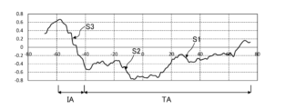
- FIG. FIG. 3 is a diagram showing a cross-sectional profile of the surface of a well layer measured with an AFM device.
- 2 is a plan view schematically showing an example of the structure of the nitride semiconductor ultraviolet light emitting device shown in FIG. 1 when viewed from above in FIG. 1.
- Each EL spectrum of the first and second metastable AlGaN becomes a composite spectrum of light emission corresponding to a plurality of AlN mole fractions changed according to the film thicknesses of the first and second metastable AlGaN shown in FIG.
- FIG. 2 is a diagram schematically showing cases in which an EL spectrum has two separated peaks and a case in which it has one peak and one shoulder peak.
- 2 is a graph showing the distribution of peak emission wavelengths of EL spectra measured in wafer states of nitride semiconductor ultraviolet light emitting devices of Examples and Comparative Examples.
- 1 is a graph showing an EL spectrum measured in a wafer state of an example of a nitride semiconductor ultraviolet light emitting device.
- FIG. 3 is a graph showing the relationship between each peak emission wavelength and film thickness of first and second metastable AlGaN.
- FIG. 3 is a diagram illustrating the relationship between the peak and shoulder peak of an EL spectrum and the minimum value of the second derivative of EL intensity.
- FIG. 1 is a cross-sectional view of essential parts schematically showing an example of the element structure of a general ultraviolet light emitting diode.
- a nitride semiconductor ultraviolet light emitting device (hereinafter simply referred to as a "light emitting device") according to an embodiment of the present invention will be described based on the drawings.
- the main parts are emphasized and the content of the invention is schematically illustrated, so the dimensional ratio of each part does not necessarily correspond to the actual element. They do not have the same size ratio.
- the present embodiment will be described below assuming that the light emitting element is a light emitting diode.
- the light emitting device 1 includes a base portion 10 including a sapphire substrate 11, and a light emitting device structure portion 20 including a plurality of AlGaN semiconductor layers 21 to 24, a p electrode 26, and an n electrode 27. Be prepared.
- the light-emitting element 1 is mounted (flip-chip mounted) with the light-emitting element structure 20 side (upper side in FIG. 1) facing a mounting base (submount, etc.), and the light extraction direction is This is the base portion 10 side (lower side in FIG. 1).
- the direction perpendicular to the main surface 11a of the sapphire substrate 11 (or the upper surface of the base part 10 and each AlGaN-based semiconductor layer 21 to 24) is referred to as the "up-down direction", and
- the direction from 10 to the light emitting element structure 20 is defined as an upward direction, and the opposite direction is defined as a downward direction.
- the base portion 10 includes a sapphire substrate 11 and an AlN layer 12 formed directly on the main surface 11a of the sapphire substrate 11.
- the sapphire substrate 11 has a main surface 11a inclined at an angle (off angle) within a certain range (for example, about 0.3° to 1° or less) with respect to the (0001) plane, and has multiple stages on the main surface 11a. This is a slightly sloped substrate with exposed terraces.
- the direction in which the off-angle is provided is determined by each direction from the AlN layer 12 to the electron block layer 23, as described later. It may be determined arbitrarily as long as multi-tiered terraces are exposed on the surface of the semiconductor layer.
- the AlN layer 12 is composed of an AlN crystal epitaxially grown from the main surface of the sapphire substrate 11, and this AlN crystal has an epitaxial crystal orientation relationship with the main surface 11a of the sapphire substrate 11. Specifically, for example, the AlN crystal is grown so that the C-axis direction ( ⁇ 0001> direction) of the sapphire substrate 11 and the C-axis direction of the AlN crystal are aligned.
- the AlN crystal constituting the AlN layer 12 may be an AlN-based semiconductor layer that may contain a trace amount of Ga or other impurities.
- the thickness of the AlN layer 12 is assumed to be approximately 2 ⁇ m to 3 ⁇ m.
- an AlGaN-based semiconductor layer may be provided between the AlN layer 12 and the AlGaN-based semiconductor layer 21 in which the AlN molar fraction is greater than or equal to the AlN molar fraction of the AlGaN-based semiconductor layer 21 .
- the AlGaN-based semiconductor layers 21 to 24 of the light emitting device structure 20 are, in order from the base portion 10 side, an n-type cladding layer 21 (n-type layer), an active layer 22, an electron block layer 23 (p-type layer), and a p-type layer. It has a structure in which type contact layers 24 (p-type layers) are sequentially grown epitaxially and stacked.
- the AlN layer 12 of the base part 10 is epitaxially grown in order from the main surface 11a of the sapphire substrate 11, the n-type cladding layer 21 of the light emitting element structure part 20, each semiconductor layer in the active layer 22, and the electronic block.
- the layer 23 has a surface on which multi-step terraces parallel to the (0001) plane originating from the main surface 11a of the sapphire substrate 11 are formed.
- the p-type contact layer 24 of the p-type layer is formed by epitaxial growth on the electron block layer 23, so similar multi-tiered terraces may be formed, but the same multi-tiered terraces are not necessarily formed. It does not need to have a surface.
- the active layer 22, the electron block layer 23, and the p-type contact layer 24 in the light-emitting element structure 20 are laminated on the second region R2 on the upper surface of the n-type cladding layer 21.
- the removed portion is removed by etching or the like and is formed on the first region R1 on the upper surface of the n-type cladding layer 21.
- the upper surface of the n-type cladding layer 21 is exposed in the second region R2 excluding the first region R1.
- the top surface of the n-type cladding layer 21 may have different heights between the first region R1 and the second region R2.
- the upper surface is defined separately in the first region R1 and the second region R2.
- the n-type cladding layer 21 is made of an n-type AlGaN-based semiconductor, and layered regions 21a having a locally low AlN mole fraction are uniformly dispersed within the n-type cladding layer 21. exist. As described above in "Background Art", the layered region 21a extends obliquely to the surface of the n-type cladding layer 21, and the band gap energy becomes locally small, so carriers are likely to be localized. It functions as a low-resistance current path.
- n-type metastable AlGaN (Al p/12 Ga 1-p/ 12 N) is predominant.
- the integer p is either 5, 6, or 7. is preferred.
- the thickness of the n-type cladding layer 21 is assumed to be approximately 1 ⁇ m to 2 ⁇ m, similar to the thickness employed in general nitride semiconductor ultraviolet light emitting devices. , may be about 2 ⁇ m to 4 ⁇ m.
- the active layer 22 includes one or more well layers 220 made of an AlGaN-based semiconductor (excluding AlN-based semiconductors and GaN-based semiconductors) and one or more barrier layers 221 made of an AlGaN-based semiconductor or an AlN-based semiconductor. It has a single quantum well structure or a multiple quantum well structure stacked alternately.
- the barrier layer 221 does not necessarily need to be provided between the bottom well layer 220 and the n-type cladding layer 21. Further, in this embodiment, the barrier layer 221 is not provided between the uppermost well layer 220 and the electron block layer 23, but in a preferred embodiment, the barrier layer 221 is thinner than the barrier layer 221 and has a higher AlN mole fraction. An AlGaN layer or an AlN layer may also be provided.
- the electron block layer 23 is made of a p-type AlGaN semiconductor.
- the p-type contact layer 24 is made of a p-type AlGaN-based semiconductor or a p-type GaN-based semiconductor.
- P-type contact layer 24 is typically made of p-GaN.
- FIG. 2 schematically shows an example of a laminated structure (multi-quantum well structure) of the well layer 220 and barrier layer 221 in the active layer 22.
- a case is illustrated in which the well layer 220 and the barrier layer 221 each have three layers. Three layers, a barrier layer 221 and a well layer 220, are laminated in this order on the n-type cladding layer 21, and the electron block layer 23 is located on the well layer 220, which is the uppermost layer.
- FIG. 3 schematically shows an example of a laminated structure (single quantum well structure) of the well layer 220 and barrier layer 221 in the active layer 22.
- a case is illustrated in which each of the well layer 220 and the barrier layer 221 is one layer.
- a barrier layer 221 and a well layer 220 are laminated in this order on the n-type cladding layer 21 .
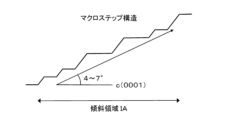
- FIG. 4 schematically shows, for example, a stepped structure (macrostep structure) exposed on the surface of the inclined region IA of one well layer 220.
- the surface of the terrace area TA (terrace T) is not a completely flat surface.
- the single step S1 and the small macro step S2 are clearly distinguished from the large macro step S3, which has a larger number of steps and forms an inclined area IA as shown in FIG.
- the height of the single step S1 and the height of one step of the small macro step S2 and the large macro step S3 of the inclined area IA are 1 ML.
- two or more stages may appear to be one stage in succession.
- Figure 6 shows the cross-sectional profile of the well layer surface measured with an AFM (Atomic Force Microscope) device.
- the units of numerical values shown on the horizontal and vertical axes are nanometers (nm).
- the horizontal axis is set to be parallel to the terrace surface, it is not perfectly aligned, and in the places shown in Figure 6, the terrace surface slopes slightly upward to the right on average with respect to the horizontal axis. It is a face.
- the existence of a large macro step S3 of about 5 to 6 steps corresponding to the slope area IA, a small macro step S2 of about 2 steps, and a single step S1 is confirmed.
- the slope area IA slopes downward to the right, whereas in the schematic diagrams of FIGS. 2 to 5, the slope is tilted upward to the right, with the left and right sides reversed. This is an above difference, not a substantive difference.
- the AlN mole fraction is reduced to the average AlN mole fraction in the well layer 220.
- a Ga-enriched well region 220a lower than Xwa is formed in the inclined region IA.
- the Ga-enriched well region 220a may also be formed in a single step S1 and a small macro step S2 within the terrace region TA.
- the density of Al increases relatively in a part of the terrace region TA.
- an Al-enriched well region is formed in which the AlN mole fraction is higher than the average AlN mole fraction Xwa.
- the average AlN mole fraction Xwa of the well layer 220 is set to 0.21 to 0.25 so that the peak emission wavelength of the EL spectrum of ultraviolet light emission from the active layer 22 is within the range of 300 nm to 320 nm. It is preferably set within a range of 0.22 or more and less than 0.25.
- metastable AlGaN Al 2/12 Ga 10/12 N having an AlN mole fraction lower than the average AlN mole fraction Xwa is formed in the Ga-enriched well region 220a, and further , metastable AlGaN Al 3/12 Ga 9/12 N is formed in the Al-enriched well region, the AlN mole fraction being higher than the average AlN mole fraction Xwa.
- the metastable AlGaN (Al 3/12 Ga 9/12 N) formed in the Al-enriched well region will be referred to as the first metastable AlGaN and the metastable AlGaN formed in the Ga-enriched well region 220a.
- Al 2/12 Ga 10/12 N are respectively referred to as second metastable AlGaN.
- the film thickness of the well layer 220 is such that the average film thickness is within the range of 2.0 nm or more and 3.5 nm or less, and the peak emission wavelength of the EL spectrum of ultraviolet light emission from the active layer 22 is within the range of 300 nm to 320 nm.
- the Al-enriched well region in the terrace region TA is adjusted such that the peak wavelength (first wavelength) of light emission (first light emission) from the first metastable AlGaN is also within the range of 300 nm to 320 nm.
- the film thickness is controlled within a predetermined range.
- the light emission from the first metastable AlGaN (first light emission) and the light emission from the second metastable AlGaN (second light emission) coexist.
- the first light emission needs to be more dominant than the second light emission.
- the EL intensity (first peak EL intensity) of the first emission at the peak wavelength (first wavelength) of the first emission is higher than that of the second emission at the peak wavelength (second wavelength) of the second emission. It needs to be larger than the EL intensity (second peak EL intensity).
- first and second peak EL intensities and the film thickness of the well layer 220 will be discussed in detail in the "EL spectrum of light emitting element" section below.
- a Ga-enriched barrier region 221a is formed in the inclined region IA, the AlN mole fraction being lower than the average AlN mole fraction Xba of the barrier layer 221. Furthermore, an Al-enriched barrier region in which the AlN mole fraction is higher than the average AlN mole fraction Xba of the barrier layer 221 may be formed in a part of the terrace region TA.
- the average AlN mole fraction Xba of the barrier layer 221 is set, for example, within the range of approximately 51% to 90%. Further, the thickness of the barrier layer 221, including the terrace area TA and the slope area IA, is set within a range of, for example, 6 nm to 8 nm.
- the electron block layer 23 similarly to the well layer 220, the electron block layer 23 includes a Ga-enriched EB region 23a in the inclined region IA, the AlN mole fraction of which is lower than the average AlN mole fraction Xea of the electron block layer 23. Further, an Al-enriched EB region having an AlN mole fraction higher than the average AlN mole fraction Xea of the electron block layer 23 may be formed in a part of the terrace region TA.
- the average AlN mole fraction Xea of the electron block layer 23 is set, for example, within the range of approximately 60% to 90%. Further, the film thickness of the electron block layer 23, including the terrace area TA and the inclined area IA, is set within a range of, for example, 15 nm to 30 nm.
- the average AlN mole fractions Xna, Xba, and Xea of the n-type cladding layer 21, the barrier layer 221, and the electron block layer 23 are the same as the average AlN mole fraction Xwa of the well layer 220. This is the target value of the AlN mole fraction at the time of forming each of the layer 221 and the electron block layer 23 or a value close to the target value.
- the p-electrode 26 is made of a multilayer metal film such as Ni/Au, and is formed on the upper surface of the p-type contact layer 24.
- the n-electrode 27 is made of a multilayer metal film such as Ti/Al/Ti/Au, and is formed in a part of the exposed surface of the second region R2 of the n-type cladding layer 21. Note that the p-electrode 26 and the n-electrode 27 are not limited to the above-described multilayer metal film, and the electrode structure such as the metal constituting each electrode, the number of laminated layers, and the laminated order may be changed as appropriate. FIG.
- FIG. 7 shows an example of the shapes of the p-electrode 26 and the n-electrode 27 when viewed from above the light emitting element 1.
- a line BL existing between the p-electrode 26 and the n-electrode 27 indicates the boundary line between the first region R1 and the second region R2. It coincides with the outer peripheral side wall surface of the contact layer 24 .
- the first region R1 and the p-electrode 26 have a comb-like shape in plan view, as an example, but the first region R1 and the p-electrode 26 have a comb-like shape in plan view.
- the visual shape, arrangement, etc. are not limited to the example shown in FIG.
- the AlN layer 12 contained in the base portion 10 and the nitride semiconductor layers 21 to 24 contained in the light emitting element structure portion 20 are epitaxially grown in order on the sapphire substrate 11 by metal organic compound vapor phase epitaxy (MOVPE) method. Layer them together.
- MOVPE metal organic compound vapor phase epitaxy
- the n-type cladding layer 21 is doped with, for example, Si as a donor impurity
- the electron block layer 23 and the p-type contact layer 24 are doped with, for example, Mg as an acceptor impurity.
- At least the surfaces of the AlN layer 12, the n-type cladding layer 21, the active layer 22 (well layer 220, barrier layer 221), and the electron block layer 23 are provided with multi-step terraces parallel to the (0001) plane.
- a slightly inclined substrate is used which is inclined in the m-axis direction or the a-axis direction and has multi-step terraces exposed on the main surface 11a.
- Conditions for such epitaxial growth include, in addition to the use of the (0001) sapphire substrate 11, which is a slightly inclined substrate, as well as a growth rate at which multi-tiered terraces are easily exposed (specifically, for example, growth temperature, source gas, carrier
- the growth rate can be achieved by appropriately setting conditions such as gas supply amount and flow rate. Note that these conditions may differ depending on the type and structure of the film forming apparatus, so it is sufficient to actually produce several samples in the film forming apparatus and specify these conditions.
- the supply amount and flow rate of the raw material gas (trimethylaluminum (TMA) gas, trimethylgallium (TMG) gas, ammonia gas) and carrier gas used in the organometallic compound vapor phase growth method are included in the above-mentioned light emitting element structure section 20.
- the average AlN mole fraction of each of the nitride semiconductor layers 21 to 24 (n-type cladding layer 21: Xna, well layer 220: Xwa, barrier layer 221: Xba, electron block layer 23: Xea) is set as a target value. .
- the optimal values of the growth rate (nm/h) and V/III ratio (supply ratio of Group V element raw material gas and Group III element raw material gas) for the nitride semiconductor layers 21 to 24 may differ for each layer.
- the average AlN mole fraction and preferred range of film thickness for each of the nitride semiconductor layers 21 to 24 have been described above in the section of "Element structure of light emitting element", so a duplicate description will be omitted.
- the growth starting point of the layered region 21a is formed by mass movement of Ga in the step portion (slanted region) between the multi-step terraces formed on the upper surface of the AlN layer 12.
- the growth temperature, growth pressure, and donor impurity concentration are adjusted so that the layered region 21a can grow obliquely upward due to segregation accompanying the mass movement of Ga as the n-type cladding layer 21 is epitaxially grown. selected.
- the growth temperature is preferably 1050° C. or higher, where Ga mass transfer easily occurs, and 1150° C. or lower, where good n-type AlGaN can be prepared.
- the growth pressure 75 Torr or less is preferable as a good AlGaN growth condition, and 10 Torr or more is realistic and preferable as the control limit of the film forming apparatus.
- the donor impurity concentration is preferably about 1 ⁇ 10 18 to 5 ⁇ 10 18 cm ⁇ 3 . Further, the donor impurity concentration does not necessarily need to be controlled uniformly in the vertical direction with respect to the thickness of the n-type cladding layer 21. Note that the above-mentioned growth temperature, growth pressure, etc. are merely examples, and the optimum conditions may be determined as appropriate depending on the film forming apparatus used.
- the entire upper surface of the n-type cladding layer 21 is coated by metal organic compound vapor phase epitaxy (MOVPE), etc.
- MOVPE metal organic compound vapor phase epitaxy
- the active layer 22 well layer 220, barrier layer 221), electron block layer 23, p-type contact layer 24, etc. are formed by the well-known epitaxial growth method.
- the acceptor impurity concentration of the electron block layer 23 is preferably about 1.0 ⁇ 10 16 to 1.0 ⁇ 10 18 cm ⁇ 3 , for example, and the acceptor impurity concentration of the p-type contact layer 24 is, for example, 1.0 About ⁇ 10 18 to 1.0 ⁇ 10 20 cm ⁇ 3 is preferable. Further, the acceptor impurity concentration does not necessarily need to be controlled uniformly in the vertical direction with respect to each film thickness of the electron block layer 23 and the p-type contact layer 24.
- the average AlN mole fraction Xwa of the well layer 220 is set to a target value under growth conditions that facilitate the exposure of the multi-tiered terraces described above.
- the well layer 220 is grown, and the barrier layer 221 is further grown with the average AlN mole fraction Xba of the barrier layer 221 set as a target value.
- the average AlN mole fraction Xwa of the well layer 220 is set within the range of 0.21 or more and less than 0.25, and as the mass of Ga moves, the Ga-enriched well region 220a, a second metastable AlGaN (Al 2/12 Ga 10/12 N) is formed whose AlN mole fraction is lower than the average AlN mole fraction A first metastable AlGaN (Al 3/12 Ga 9/12 N) with a mole fraction higher than Xwa is formed.
- the first emission from the first metastable AlGaN is more dominant than the second emission from the second metastable AlGaN, as described above.
- the upper limit of the off-angle of the sapphire substrate 11 is limited to about 1°, and furthermore, in order to prevent the second emission from becoming more dominant than the first emission, the second metastable AlGaN
- the electron block layer 23 is formed in the same manner as the n-type cladding layer 21, under growth conditions that facilitate the exposure of the multi-tiered terraces described above, with the average AlN mole fraction Xea of the electron block layer 23 set to a target value. Grow layer 23.
- the second region R2 of the nitride semiconductor layers 21 to 24 is selectively etched using a well-known etching method such as reactive ion etching until the upper surface of the n-type cladding layer 21 is exposed. The second region R2 portion of the upper surface is exposed.
- a p-electrode 26 is formed on the p-type contact layer 24 in the unetched first region R1, and an n-type contact layer 26 is formed in the etched first region R2.
- An n-electrode 27 is formed on the mold cladding layer 21. Note that after forming one or both of the p-electrode 26 and the n-electrode 27, heat treatment may be performed using a well-known heat treatment method such as RTA (instant thermal annealing).
- the light emitting element 1 is, for example, flip-chip mounted on a base such as a submount, and then sealed with a predetermined resin (for example, lens-shaped resin) such as silicone resin or amorphous fluororesin. Can be used in any state.
- a predetermined resin for example, lens-shaped resin
- silicone resin or amorphous fluororesin.
- a single step S1, a small macro step S2, and a large macro step S3 are formed in the terrace region TA and slope region IA of the well layer 220, and the surface of the well layer 220 is formed with a single step S1, a small macro step S2, and a large macro step S3.
- FIG. 5 As an example, as schematically shown in FIG.
- the film thickness tT1 There may be a film thickness tT0 of (m-1) ML that is 1 ML thinner.
- m is an integer within the range of 8 to 14.
- the film thickness tS1 is There may be a film thickness tS0 of ML that is 1 ML thinner (m+k-1), a film thickness tS2 of (m+k+1) ML that is 1 ML thicker than film thickness tS1, and a film thickness tS3 of ML that is 2 ML thicker than film thickness tS1 (m+k+2).
- k is an integer greater than or equal to 0, and tends to increase as the mass transfer of Ga increases. In one embodiment, k is assumed to be approximately 1 to 4.
- the EL spectrum of the ultraviolet light emitted from the active layer 22 is a composite spectrum of the EL spectrum of the first light emission (ELS1) and the EL spectrum of the second light emission (ELS2).
- the emission from the main film thickness tT1 of the Al-enriched well region is dominant.
- the peak emission wavelength ⁇ (3, m) of the EL spectrum of the film thickness tT1 (mML) does not necessarily match the peak emission wavelength (first wavelength, ⁇ 1) of the EL spectrum of the first emission (ELS1), and the offset of ⁇ 3 may occur.
- the offset ⁇ 3 changes from die to die of the light emitting element 1 within the wafer due to variations within the wafer, such as the thickness of the well layer 220 and the degree of mass transfer of Ga.
- the emission from the main thickness tS1 of the Ga-enriched well region 220a is dominant.
- the peak emission wavelength ⁇ (2, m+k) of the EL spectrum of the film thickness tS1 ((m+k)ML) does not necessarily match the peak emission wavelength (second wavelength, ⁇ 2) of the EL spectrum (ELS2) of the second emission,
- An offset of ⁇ 2 may occur.
- the offset ⁇ 2 changes from die to die of the light emitting element 1 within the wafer due to variations within the wafer, such as the thickness of the well layer 220 and the degree of mass transfer of Ga.
- the EL spectrum of the first emission (ELS1) and the EL spectrum of the second emission (ELS2) are separated into two peaks, each of which is an independent peak.
- An example is given below.
- the degree of mass movement of Ga within the wafer varies.
- the difference between the peak emission wavelength ⁇ 1 of the first emission and the peak emission wavelength ⁇ 2 of the second emission becomes shorter and the EL intensity of the second emission decreases relative to the first emission, the EL of the second emission decreases.
- the peak of the spectrum does not appear as an independent peak separated from the EL spectrum (ELS1) of the first emission as schematically shown on the left side of FIG. 10, but as shown schematically on the right side of FIG. This may appear as a bulge (shoulder peak) in the emission intensity at the shoulder portion on the long wavelength side of the EL spectrum of the first emission (ELS1).
- an independent peak is defined as a condition where, when the wavelength of the EL spectrum monotonically increases from the wavelength side shorter than the wavelength of the independent peak (peak wavelength), the EL intensity monotonically increases until the wavelength reaches the peak wavelength. It is defined as the peak at the peak wavelength when the wavelength increases, takes a maximum value when the wavelength reaches the peak wavelength, and monotonically decreases as the wavelength increases further beyond the peak wavelength.
- the peak of the EL spectrum (ELS2) of the second emission is equal to the peak of the EL spectrum of the first emission.
- the EL intensity of the EL spectrum of the ultraviolet light emitted from the active layer 22 is expressed as a function with wavelength as a variable, and a plurality of extreme points that take a minimum value in the second derivative of the EL intensity are extracted.
- the first wavelength ⁇ 1 is specified as the wavelength of the extreme value point having the smallest minimum value among the plurality of extreme value points.
- the second wavelength ⁇ 2 is the minimum value of one or more extreme points existing on the longer wavelength side than a reference wavelength that is 10 nm longer than the first wavelength ⁇ 1 selected from the plurality of extreme points. Specified as the wavelength of the value point.
- the identification method even if there are a total of three or more independent peaks and shoulder peaks, the first wavelength ⁇ 1 and the second wavelength ⁇ 2 can be accurately identified. For example, if the EL spectrum has a shoulder peak originating from the first emission at a shorter wavelength or longer wavelength than the first wavelength ⁇ 1, or if there is a small peak due to measurement error in the second derivative of the EL intensity. Even if a value point exists, the wavelength of the shoulder peak or minute extreme point is prevented from being erroneously specified as the second wavelength ⁇ 2.
- a specific example of the first wavelength ⁇ 1 and second wavelength ⁇ 2 according to the identification method will be described later with reference to FIG. 14.
- the first wavelength ⁇ 1 is not determined by the specific method, but is determined by the wavelength at which the EL intensity is the maximum value, or the EL intensity at the zero point among one or more zero points in the first derivative of the EL intensity. It can also be specified as a wavelength.
- the second light emission peak is an independent peak
- the second wavelength ⁇ 2 is also the wavelength of the maximum point where the EL intensity is the maximum value in the wavelength range on the longer wavelength side than the first wavelength ⁇ 1, or the wavelength of the maximum point of the EL It can also be specified as a wavelength at which the EL intensity at the zero point has a maximum value among one or more zero points in the first derivative of intensity.
- each wafer about 40 chips are selected from among the chips with an external quantum efficiency of 0.03% or more along the inflow direction of the raw material gas on the center line of the wafer, and the EL spectra of a total of about 120 chips are obtained. , was measured using an autoprober attached to a spectrometer. The wavelength resolution of the spectrometer used was 0.8 nm.
- the three types of wafers W1, W2, and WR used to measure the EL spectra each have, in order from the bottom, an n-type cladding layer 21, a barrier layer 221, a well layer 220, an AlN layer 223, an electron block layer 23, and a p
- the light emitting device structure 20 shown in FIG. 3 is provided with a type contact layer 24 stacked thereon, and the active layer 22 is a single quantum well structure consisting of one well layer 220 and one barrier layer 221.
- the average AlN mole fraction Xna of the n-type cladding layer 21 is about 45%, and the film thickness is 1.7 ⁇ m.
- the average AlN mole fraction Xba of the barrier layer 221 is about 67%, and the film thickness is about 8 nm.
- the average AlN mole fraction Xnw of the well layer 220 is about 21 to 24%, and the film thickness varies between wafers and within a wafer. It is estimated to be within the range of 2.5 to 3.5 nm based on the growth conditions.
- the thickness of the AlN layer 223 is about 2 nm.
- the average AlN mole fraction Xea of the electron block layer 23 is about 67%, and the film thickness is about 30 nm.
- the p-type contact layer 24 is composed of a p-type GaN layer with a thickness of approximately 25 nm.
- FIG. 11 shows the distribution state of the peak emission wavelength of each chip (before dicing) in the wafer state of three types of wafers W1, W2, and WR.
- the vertical axis indicates the peak emission wavelength (nm)
- the horizontal axis indicates the position of each chip within the wafer.
- two large and small white circles indicate the peak emission wavelength of the wafer W1
- two large and small black circles indicate the peak emission wavelength of the wafer W1
- an x mark indicates the peak emission wavelength of the wafer WR. From FIG.
- the first emission from the first metastable AlGaN and the second emission from the second metastable AlGaN coexist in the EL spectrum, so the first emission In the case of wafer W1, the first wavelength ⁇ 1, which is the peak wavelength of In the case of wafer W1, the second wavelength ⁇ 2, which is the peak wavelength of the second light emission, falls within the range of 323 nm to 329 nm, excluding the two chips at the edge of the wafer, and in the case of wafer W2, the second wavelength ⁇ 2, which is the peak wavelength of the second light emission, falls within the range of 323 nm to 329 nm, excluding the two chips at the edge of the wafer.
- the wavelength is within the range of 324 nm to 335 nm, except for one chip at each end. Further, the difference between the first wavelength ⁇ 1 and the second wavelength ⁇ 2 is within the range of 17 nm to 26 nm, except for the specific few chips at the wafer edge and the like. Note that the peak at the second wavelength ⁇ 2 of the second light emission includes both an independent peak and a shoulder peak.
- each of the semiconductor layers 21 to 24 of the light emitting element structure 20 has a surface on which multi-step terraces parallel to the (0001) plane are formed.
- the mass transfer of Ga within the well layer 220 does not occur significantly to the extent that the second metastable AlGaN is formed, and as a result, in the EL spectrum of each chip, the 2. No second emission from metastable AlGaN was confirmed. From FIG. 11, it can be seen that in the case of the wafer WR of the comparative example, the first wavelength ⁇ 1, which is the peak wavelength of the first light emission, falls within the range of 301 nm to 311 nm. It is reported in the above-mentioned Non-Patent Document 3 that multi-step terraces parallel to the (0001) plane are not formed in a sapphire substrate with an off-angle of 0.3° or less.
- the off-angle of the sapphire substrate used was only 1.0°, but as the off-angle increased beyond 1.0°, the mass transfer of Ga was further promoted. Therefore, the peak of the second emission from the second metastable AlGaN becomes a prominent independent peak and can be more dominant than the first emission from the first metastable AlGaN. Therefore, the off-angle of the sapphire substrate is 1 It is preferable that the angle is .0° or less.
- the EL intensity at the second wavelength ⁇ 2 of the second light emission from the second metastable AlGaN is equal to the first wavelength of the first light emission from the first metastable AlGaN. Since there are some chips that are larger than the EL intensity at ⁇ 1 (first peak EL intensity), the off-angle of the sapphire substrate is more preferably less than 1.0°, and is 0.9° or less. It is even more preferable.
- the off-angle of the sapphire substrate needs to be larger than 0.3°.
- the AFM image of the surface of the AlN layer formed on the sapphire substrate with an off angle of 0.3° shown in FIG. 2(b) of Non-Patent Document 3, shows that there are hexagonal
- the formation of columnar or hexagonal pyramid-shaped hillocks can be seen, as well as signs of triangular facets, which are traces of step-flow growth that forms multi-tiered terraces.
- FIG. 1 shows that there are hexagonal The formation of columnar or hexagonal pyramid-shaped hillocks can be seen, as well as signs of triangular facets, which are traces of step-flow growth that forms multi-tiered terraces.
- the AFM image of the surface of the AlN layer formed on the sapphire substrate with an off angle of 0.48° shows the multi-step terraces and triangular facets. It can be confirmed that it is clearly formed. Therefore, the lower limit of the off-angle of the sapphire substrate is determined on the condition that multi-step terraces are formed parallel to the (0001) plane, and the value is greater than 0.3° and approximately 0.35° to 0.45°. Estimated to be within a range of °.
- FIG. 12 shows the EL spectra of 3 chips (S11 to S13) of wafer W1 and 6 chips (S21 to S26) of wafer W2 selected from the two types of wafers W1 and W2 of the light emitting element 1 for each wafer.
- the EL spectra of a plurality of chips within the same wafer are displayed overlappingly with their vertical axes shifted so that they are S11 to S13 and S21 to S26 in order from the bottom.
- the vertical axis in FIG. 12 is the normalized EL intensity, and the horizontal axis is the wavelength (nm).
- Table 1 shows the peak emission wavelength (first wavelength, ⁇ 1) of the first emission using the second derivative of the EL intensity for the EL spectra of the nine chips selected from wafers W1 and W2. The results of calculating the peak emission wavelength (second wavelength, ⁇ 2) of the second emission are shown.
- the thickness of the well layer 220 was varied within the range of 6 ML to 15 ML.
- the relaxation rate fR was set to 0.5 in consideration of the device structures and growth conditions of the two types of wafers W1 and W2 of the light emitting device 1.
- the peak emission wavelength of light emission from the first metastable AlGaN ⁇ (3, m) and the peak emission wavelength of light emission from the second metastable AlGaN ⁇ ( 2, m+k) are shown in Tables 3 and 4.
- the film thickness of the Al-enriched well region (mainly the terrace region TA excluding the single step S1 and small macro step S2) of the well layer 220 in which the first metastable AlGaN is formed. It can be seen that for the wafer W1, the distribution is within the range of 9 to 10 ML, and for the wafer W2, it is distributed within the range of 10 to 12 ML. Furthermore, the film thickness of the Ga-enriched well region 220a (mainly the single step S1, small macro step S2, and inclined region IA) of the well layer 220 in which the second metastable AlGaN is formed is 12 to 13 ML in the wafer W1. It can be seen that the distribution is within a range of 12 to 15 ML for wafer W2.
- the average film thickness tARa of the Al-enriched well region 220a and the average film thickness tGRa of the Ga-enriched well region 220a for each chip are determined from the relationship between the peak emission wavelength and film thickness shown in FIG. can be derived as the film thickness corresponding to the second wavelength ⁇ 2. From the results shown in Tables 3 and 4, it can be seen that the average thickness tARa of the Al-enriched well region is smaller than the average thickness tGRa of the Ga-enriched well region 220a.
- the average film thickness of the well layer 220 over the terrace region TA and the slope region IA can be estimated from the growth conditions of the well layer 220, it is difficult to accurately measure it.
- the area of the terrace region TA and the slope region IA shown in the entire well layer 220 is several times larger than the area of the slope region IA, so the average film thickness tQWa of the well layer 220 is
- the average film thickness tARa of the Al-enriched well region is closer to the average film thickness tARa of the Al-enriched well region than the average value tAGa of the average film thickness tARa of the enriched well region and the average film thickness tGRa of the Ga-enriched well region 220a.
- the second derivative of the EL intensity of the EL spectrum of the ultraviolet emission from the active layer 22 described above It is assumed that it has become clear that the first wavelength ⁇ 1 and the second wavelength ⁇ 2 can be calculated using .
- the first light emission from the first metastable AlGaN and the second light emission from the second metastable AlGaN coexist.
- the feature is that the first light emission is more dominant than the second light emission.
- the AlN mole fraction of the AlGaN-based semiconductor constituting the well layer 220 is lower than in a case where the peak emission wavelength is less than about 285 nm.
- the holes that reach the terrace region TA in the well layer 220 are recombined radiatively in the terrace region TA where the mole fraction of AlN is higher than that in the inclined region IA.
- Light emission occurs at a shorter wavelength than the inclined region IA.
- the light emitting element 1 effectively utilizes the emission recombination in the terrace area TA to realize a peak emission wavelength of around 310 nm with high internal quantum efficiency.
- the p-type layer constituting the light-emitting device structure 20 was two layers, the electron block layer 23 and the p-type contact layer 24, but the electron block layer 23 and the p-type A configuration may also be adopted in which one or more p-type cladding layers made of a p-type AlGaN-based semiconductor are provided between the contact layers 24.
- Mg can be used similarly to the electron block layer 23 and the p-type contact layer 24.
- the p-type cladding layer is active with the AlN layer 12 of the base portion 10 and the n-type cladding layer 21 of the light emitting element structure portion 20, which are epitaxially grown in order from the main surface 11a of the sapphire substrate 11.
- the p-type cladding layer is active with the AlN layer 12 of the base portion 10 and the n-type cladding layer 21 of the light emitting element structure portion 20, which are epitaxially grown in order from the main surface 11a of the sapphire substrate 11.
- the p-type cladding layer is active with the AlN layer 12 of the base portion 10 and the n-type cladding layer 21 of the light emitting element structure portion 20, which are epitaxially grown in order from the main surface 11a of the sapphire substrate 11.
- the p-type cladding layer is active with the AlN layer 12 of the base portion 10 and the n-type cladding layer 21 of the light emitting element structure portion 20, which are epitaxially grown in order from the main surface 11
- the average AlN mole fraction of the p-type cladding layer is set within the range of approximately 52% to 74%, and the film thickness is set within the range of 20 nm to 200 nm, for example.
- the supply amount and flow rate of the raw material gas and carrier gas used in the organometallic compound vapor phase epitaxy are such that the n-type cladding layer 21 is formed. It has been explained that it is set according to the average AlN mole fraction of the entire n-type AlGaN layer. In other words, if the average AlN mole fraction of the entire n-type cladding layer 21 is set to a constant value in the vertical direction, it is assumed that the supply amount and flow rate of the raw material gas etc. are controlled to be constant. . However, the supply amount and flow rate of the raw material gas etc. do not necessarily have to be controlled to be constant.
- the first region R1 and the p-electrode 26 have, for example, a comb shape in plan view, but the plan view shape is not limited to the comb shape.
- a plurality of first regions R1 may exist, each surrounded by one second region R2 in a plan view shape.
- the light emitting element 1 includes the base part 10 including the sapphire substrate 11. 10) may be removed by lift-off or the like. Furthermore, the substrate constituting the base portion 10 is not limited to a sapphire substrate.
- the present invention provides a light emitting device structure having a light emitting device structure in which an n-type layer, an active layer, and a p-type layer made of an AlGaN-based semiconductor with a wurtzite structure are stacked in the vertical direction. It can be used in existing nitride semiconductor ultraviolet light emitting devices.
- Nitride semiconductor ultraviolet light emitting device 10 Base portion 11: Sapphire substrate 11a: Main surface of sapphire substrate 12: AlN layer 20: Light emitting device structure portion 21: N-type cladding layer (n-type layer) 21a: Layered region (n-type layer) 21b: n-type main body region (n-type layer) 22: Active layer 220: Well layer 220a: Ga-enriched well region 221: Barrier layer 221a: Ga-enriched barrier region 223: AlN layer 23: Electron blocking layer (p-type layer) 23a: Ga-enriched EB region 24: p-type contact layer (p-type layer) 26: p-electrode 27: n-electrode 100: substrate 101: AlGaN-based semiconductor layer 102: template 103: n-type AlGaN-based semiconductor layer 104: active layer 105: p-type AlGaN-based semiconductor layer 106: p-type contact layer 107: n-electrode 108: P electrode BL
Landscapes
- Led Devices (AREA)
- Semiconductor Lasers (AREA)
Priority Applications (3)
| Application Number | Priority Date | Filing Date | Title |
|---|---|---|---|
| PCT/JP2022/018020 WO2023203599A1 (ja) | 2022-04-18 | 2022-04-18 | 窒化物半導体紫外線発光素子 |
| JP2024515747A JP7614449B2 (ja) | 2022-04-18 | 2022-04-18 | 窒化物半導体紫外線発光素子 |
| TW111142152A TWI919016B (zh) | 2022-04-18 | 2022-11-04 | 氮化物半導體紫外光發光元件 |
Applications Claiming Priority (1)
| Application Number | Priority Date | Filing Date | Title |
|---|---|---|---|
| PCT/JP2022/018020 WO2023203599A1 (ja) | 2022-04-18 | 2022-04-18 | 窒化物半導体紫外線発光素子 |
Publications (1)
| Publication Number | Publication Date |
|---|---|
| WO2023203599A1 true WO2023203599A1 (ja) | 2023-10-26 |
Family
ID=88419391
Family Applications (1)
| Application Number | Title | Priority Date | Filing Date |
|---|---|---|---|
| PCT/JP2022/018020 Ceased WO2023203599A1 (ja) | 2022-04-18 | 2022-04-18 | 窒化物半導体紫外線発光素子 |
Country Status (2)
| Country | Link |
|---|---|
| JP (1) | JP7614449B2 (https=) |
| WO (1) | WO2023203599A1 (https=) |
Cited By (1)
| Publication number | Priority date | Publication date | Assignee | Title |
|---|---|---|---|---|
| JP2025119282A (ja) * | 2024-02-01 | 2025-08-14 | 日機装株式会社 | 発光素子及び外観検査方法 |
Citations (6)
| Publication number | Priority date | Publication date | Assignee | Title |
|---|---|---|---|---|
| WO2019159265A1 (ja) * | 2018-02-14 | 2019-08-22 | 創光科学株式会社 | 窒化物半導体紫外線発光素子 |
| WO2021260849A1 (ja) * | 2020-06-24 | 2021-12-30 | 創光科学株式会社 | 窒化物半導体紫外線発光素子 |
| WO2021260850A1 (ja) * | 2020-06-24 | 2021-12-30 | 創光科学株式会社 | 窒化物半導体紫外線発光素子及びその製造方法 |
| WO2022009306A1 (ja) * | 2020-07-07 | 2022-01-13 | 創光科学株式会社 | 窒化物半導体紫外線発光素子及びその製造方法 |
| WO2022038769A1 (ja) * | 2020-08-21 | 2022-02-24 | 創光科学株式会社 | 窒化物半導体紫外線発光素子 |
| WO2022059125A1 (ja) * | 2020-09-17 | 2022-03-24 | 創光科学株式会社 | 窒化物半導体紫外線発光素子 |
-
2022
- 2022-04-18 WO PCT/JP2022/018020 patent/WO2023203599A1/ja not_active Ceased
- 2022-04-18 JP JP2024515747A patent/JP7614449B2/ja active Active
Patent Citations (6)
| Publication number | Priority date | Publication date | Assignee | Title |
|---|---|---|---|---|
| WO2019159265A1 (ja) * | 2018-02-14 | 2019-08-22 | 創光科学株式会社 | 窒化物半導体紫外線発光素子 |
| WO2021260849A1 (ja) * | 2020-06-24 | 2021-12-30 | 創光科学株式会社 | 窒化物半導体紫外線発光素子 |
| WO2021260850A1 (ja) * | 2020-06-24 | 2021-12-30 | 創光科学株式会社 | 窒化物半導体紫外線発光素子及びその製造方法 |
| WO2022009306A1 (ja) * | 2020-07-07 | 2022-01-13 | 創光科学株式会社 | 窒化物半導体紫外線発光素子及びその製造方法 |
| WO2022038769A1 (ja) * | 2020-08-21 | 2022-02-24 | 創光科学株式会社 | 窒化物半導体紫外線発光素子 |
| WO2022059125A1 (ja) * | 2020-09-17 | 2022-03-24 | 創光科学株式会社 | 窒化物半導体紫外線発光素子 |
Cited By (2)
| Publication number | Priority date | Publication date | Assignee | Title |
|---|---|---|---|---|
| JP2025119282A (ja) * | 2024-02-01 | 2025-08-14 | 日機装株式会社 | 発光素子及び外観検査方法 |
| JP7737484B2 (ja) | 2024-02-01 | 2025-09-10 | 日機装株式会社 | 発光素子及び外観検査方法 |
Also Published As
| Publication number | Publication date |
|---|---|
| JP7614449B2 (ja) | 2025-01-15 |
| TW202343828A (zh) | 2023-11-01 |
| JPWO2023203599A1 (https=) | 2023-10-26 |
Similar Documents
| Publication | Publication Date | Title |
|---|---|---|
| JP5881222B2 (ja) | 窒化物半導体紫外線発光素子及び窒化物半導体紫外線発光素子の製造方法 | |
| CN104364917B (zh) | 氮化物半导体发光元件及其制造方法 | |
| TWI684291B (zh) | 氮化物半導體紫外線發光元件 | |
| US20060060833A1 (en) | Radiation-emitting optoelectronic component with a quantum well structure and method for producing it | |
| TWI707482B (zh) | 氮化物半導體發光元件 | |
| JP2011060917A (ja) | 半導体発光素子 | |
| TWI828945B (zh) | 氮化物半導體紫外線發光元件 | |
| JP7614449B2 (ja) | 窒化物半導体紫外線発光素子 | |
| JP7421657B2 (ja) | 窒化物半導体紫外線発光素子 | |
| CN105742442B (zh) | 氮化物半导体紫外线发光元件的制造方法 | |
| TWI851832B (zh) | 氮化物半導體紫外線發光元件及其製造方法 | |
| JP6486401B2 (ja) | 半導体発光素子および半導体発光素子の製造方法 | |
| TWI881114B (zh) | 氮化物半導體紫外線發光元件及其製造方法 | |
| WO2011101929A1 (ja) | 半導体発光装置及びその製造方法 | |
| TWI919016B (zh) | 氮化物半導體紫外光發光元件 | |
| KR100742989B1 (ko) | 질화갈륨계 발광 소자의 제조 방법 | |
| JP7672778B2 (ja) | 窒化物半導体紫外線発光素子の製造方法、及び、窒化物半導体紫外線発光素子 |
Legal Events
| Date | Code | Title | Description |
|---|---|---|---|
| 121 | Ep: the epo has been informed by wipo that ep was designated in this application |
Ref document number: 22938402 Country of ref document: EP Kind code of ref document: A1 |
|
| ENP | Entry into the national phase |
Ref document number: 2024515747 Country of ref document: JP Kind code of ref document: A |
|
| NENP | Non-entry into the national phase |
Ref country code: DE |
|
| 122 | Ep: pct application non-entry in european phase |
Ref document number: 22938402 Country of ref document: EP Kind code of ref document: A1 |