WO2023203599A1 - Nitride semiconductor ultraviolet light-emitting diode - Google Patents
Nitride semiconductor ultraviolet light-emitting diode Download PDFInfo
- Publication number
- WO2023203599A1 WO2023203599A1 PCT/JP2022/018020 JP2022018020W WO2023203599A1 WO 2023203599 A1 WO2023203599 A1 WO 2023203599A1 JP 2022018020 W JP2022018020 W JP 2022018020W WO 2023203599 A1 WO2023203599 A1 WO 2023203599A1
- Authority
- WO
- WIPO (PCT)
- Prior art keywords
- layer
- wavelength
- emission
- algan
- peak
- Prior art date
Links
- 239000004065 semiconductor Substances 0.000 title claims abstract description 127
- 150000004767 nitrides Chemical class 0.000 title claims abstract description 53
- 238000001194 electroluminescence spectrum Methods 0.000 claims abstract description 79
- 229910002704 AlGaN Inorganic materials 0.000 claims abstract 5
- 239000000758 substrate Substances 0.000 claims description 46
- 229910052594 sapphire Inorganic materials 0.000 claims description 36
- 239000010980 sapphire Substances 0.000 claims description 36
- 239000010410 layer Substances 0.000 description 407
- 235000012431 wafers Nutrition 0.000 description 58
- 238000005253 cladding Methods 0.000 description 49
- 230000004888 barrier function Effects 0.000 description 34
- 239000012535 impurity Substances 0.000 description 15
- 235000017399 Caesalpinia tinctoria Nutrition 0.000 description 14
- 241000388430 Tara Species 0.000 description 14
- 238000000034 method Methods 0.000 description 14
- 239000013078 crystal Substances 0.000 description 13
- 239000007789 gas Substances 0.000 description 11
- 229910052782 aluminium Inorganic materials 0.000 description 9
- 238000010586 diagram Methods 0.000 description 8
- 238000005204 segregation Methods 0.000 description 8
- 239000002994 raw material Substances 0.000 description 7
- 238000009826 distribution Methods 0.000 description 6
- 229910052733 gallium Inorganic materials 0.000 description 6
- 239000000203 mixture Substances 0.000 description 5
- 229910052757 nitrogen Inorganic materials 0.000 description 5
- 238000001228 spectrum Methods 0.000 description 5
- 230000000052 comparative effect Effects 0.000 description 4
- 230000007423 decrease Effects 0.000 description 4
- 229910021478 group 5 element Inorganic materials 0.000 description 4
- 229910052751 metal Inorganic materials 0.000 description 4
- 239000002184 metal Substances 0.000 description 4
- 150000002902 organometallic compounds Chemical class 0.000 description 4
- 238000004088 simulation Methods 0.000 description 4
- 230000015572 biosynthetic process Effects 0.000 description 3
- 239000000969 carrier Substances 0.000 description 3
- 239000002131 composite material Substances 0.000 description 3
- 238000005530 etching Methods 0.000 description 3
- 238000004519 manufacturing process Methods 0.000 description 3
- 238000005259 measurement Methods 0.000 description 3
- 230000006798 recombination Effects 0.000 description 3
- 238000005215 recombination Methods 0.000 description 3
- 238000000927 vapour-phase epitaxy Methods 0.000 description 3
- 229910052984 zinc sulfide Inorganic materials 0.000 description 3
- 238000000089 atomic force micrograph Methods 0.000 description 2
- 230000000903 blocking effect Effects 0.000 description 2
- 210000000746 body region Anatomy 0.000 description 2
- 239000012159 carrier gas Substances 0.000 description 2
- 238000005401 electroluminescence Methods 0.000 description 2
- 238000010438 heat treatment Methods 0.000 description 2
- 229920005989 resin Polymers 0.000 description 2
- 239000011347 resin Substances 0.000 description 2
- 238000007619 statistical method Methods 0.000 description 2
- XCZXGTMEAKBVPV-UHFFFAOYSA-N trimethylgallium Chemical compound C[Ga](C)C XCZXGTMEAKBVPV-UHFFFAOYSA-N 0.000 description 2
- QGZKDVFQNNGYKY-UHFFFAOYSA-N Ammonia Chemical compound N QGZKDVFQNNGYKY-UHFFFAOYSA-N 0.000 description 1
- 206010012438 Dermatitis atopic Diseases 0.000 description 1
- 238000000137 annealing Methods 0.000 description 1
- 201000008937 atopic dermatitis Diseases 0.000 description 1
- 230000007547 defect Effects 0.000 description 1
- 238000000151 deposition Methods 0.000 description 1
- 238000005566 electron beam evaporation Methods 0.000 description 1
- 238000000605 extraction Methods 0.000 description 1
- 210000003918 fraction a Anatomy 0.000 description 1
- 229910052738 indium Inorganic materials 0.000 description 1
- 230000004807 localization Effects 0.000 description 1
- 238000004020 luminiscence type Methods 0.000 description 1
- 230000002093 peripheral effect Effects 0.000 description 1
- 238000001020 plasma etching Methods 0.000 description 1
- 229920002050 silicone resin Polymers 0.000 description 1
- 239000002356 single layer Substances 0.000 description 1
- 230000003595 spectral effect Effects 0.000 description 1
- JLTRXTDYQLMHGR-UHFFFAOYSA-N trimethylaluminium Chemical compound C[Al](C)C JLTRXTDYQLMHGR-UHFFFAOYSA-N 0.000 description 1
- 238000001947 vapour-phase growth Methods 0.000 description 1
- 230000000007 visual effect Effects 0.000 description 1
Images


Classifications
-
- H—ELECTRICITY
- H01—ELECTRIC ELEMENTS
- H01L—SEMICONDUCTOR DEVICES NOT COVERED BY CLASS H10
- H01L33/00—Semiconductor devices with at least one potential-jump barrier or surface barrier specially adapted for light emission; Processes or apparatus specially adapted for the manufacture or treatment thereof or of parts thereof; Details thereof
- H01L33/02—Semiconductor devices with at least one potential-jump barrier or surface barrier specially adapted for light emission; Processes or apparatus specially adapted for the manufacture or treatment thereof or of parts thereof; Details thereof characterised by the semiconductor bodies
- H01L33/20—Semiconductor devices with at least one potential-jump barrier or surface barrier specially adapted for light emission; Processes or apparatus specially adapted for the manufacture or treatment thereof or of parts thereof; Details thereof characterised by the semiconductor bodies with a particular shape, e.g. curved or truncated substrate
- H01L33/24—Semiconductor devices with at least one potential-jump barrier or surface barrier specially adapted for light emission; Processes or apparatus specially adapted for the manufacture or treatment thereof or of parts thereof; Details thereof characterised by the semiconductor bodies with a particular shape, e.g. curved or truncated substrate of the light emitting region, e.g. non-planar junction
-
- H—ELECTRICITY
- H01—ELECTRIC ELEMENTS
- H01L—SEMICONDUCTOR DEVICES NOT COVERED BY CLASS H10
- H01L33/00—Semiconductor devices with at least one potential-jump barrier or surface barrier specially adapted for light emission; Processes or apparatus specially adapted for the manufacture or treatment thereof or of parts thereof; Details thereof
- H01L33/02—Semiconductor devices with at least one potential-jump barrier or surface barrier specially adapted for light emission; Processes or apparatus specially adapted for the manufacture or treatment thereof or of parts thereof; Details thereof characterised by the semiconductor bodies
- H01L33/26—Materials of the light emitting region
- H01L33/30—Materials of the light emitting region containing only elements of group III and group V of the periodic system
- H01L33/32—Materials of the light emitting region containing only elements of group III and group V of the periodic system containing nitrogen
Definitions
- the present invention provides a light emitting device structure having a light emitting device structure in which an n-type layer, an active layer, and a p-type layer made of an AlGaN-based semiconductor with a wurtzite structure are stacked in the vertical direction.
- This invention relates to existing nitride semiconductor ultraviolet light emitting devices.
- nitride semiconductor light emitting devices in which a light emitting device structure consisting of a plurality of nitride semiconductor layers is formed by epitaxial growth on a substrate such as sapphire.
- the nitride semiconductor layer is represented by the general formula Al 1-xy Ga x In y N (0 ⁇ x ⁇ 1, 0 ⁇ y ⁇ 1, 0 ⁇ x+y ⁇ 1).
- the light emitting element structure of a light emitting diode has a double heterostructure in which an active layer made of a nitride semiconductor layer is sandwiched between two cladding layers, an n-type nitride semiconductor layer and a p-type nitride semiconductor layer.
- the active layer is an AlGaN-based semiconductor
- the AlN mole fraction also called Al composition ratio
- the band gap energy can be changed to the band gap energy that GaN and AlN can take (approximately 3.4 eV and approximately 6.2 eV).
- an ultraviolet light emitting device with an emission wavelength of about 200 nm to about 365 nm can be obtained.
- a forward current from the p-type nitride semiconductor layer to the n-type nitride semiconductor layer, the recombination of carriers (electrons and holes) in the active layer is performed according to the above band gap energy. Luminescence occurs.
- a p-electrode is provided on the p-type nitride semiconductor layer, and an n-electrode is provided on the n-type nitride semiconductor layer.
- the active layer is an AlGaN-based semiconductor
- the n-type nitride semiconductor layer and the p-type nitride semiconductor layer sandwiching the active layer are composed of AlGaN-based semiconductors having a higher AlN mole fraction than the active layer.
- a p-type nitride semiconductor layer with a high AlN mole fraction is added to the top layer of the p-type nitride semiconductor layer.
- a p-type contact layer that can make good ohmic contact with a p-electrode made of an AlGaN-based semiconductor (specifically, p-GaN). Since the AlN mole fraction of this p-type contact layer is smaller than that of the AlGaN-based semiconductor constituting the active layer, ultraviolet rays emitted from the active layer toward the p-type nitride semiconductor layer are absorbed by the p-type contact layer. , cannot be effectively taken out to the outside of the device. For this reason, a typical ultraviolet light emitting diode whose active layer is an AlGaN-based semiconductor adopts a device structure as schematically shown in FIG. is effectively taken out to the outside of the device (for example, see Patent Documents 1 to 3 below).
- a typical ultraviolet light emitting diode has an n-type AlGaN-based semiconductor layer 101 (for example, an AlN layer) deposited on a template 102 formed by depositing an AlGaN-based semiconductor layer 101 (for example, an AlN layer) on a substrate 100 such as a sapphire substrate.
- a semiconductor layer 103, an active layer 104, a p-type AlGaN-based semiconductor layer 105, and a p-type contact layer 106 are deposited in order, and a part of the active layer 104, p-type AlGaN-based semiconductor layer 105, and p-type contact layer 106 are deposited.
- compositional modulation occurs due to Ga segregation (segregation due to mass movement of Ga), and local AlN moles extending obliquely to the cladding layer surface occur. It has been reported that a layered region with a low fraction is formed (for example, see Patent Document 4, Non-Patent Documents 1 and 2, etc. below).
- multi-tiered terraces parallel to the (0001) plane are exposed on the surface of each layer of the active layer of the multi-quantum well structure formed on the n-type cladding layer, and each layer of the active layer is formed on the n-type cladding layer.
- a region with a relatively low AlN mole fraction is generated in a slope region that is inclined with respect to the (0001) plane connecting adjacent terraces, and a region with a relatively low AlN mole fraction is generated in the terrace region.
- Non-Patent Document 1 It is reported in Non-Patent Document 1 that overlap may occur.
- Patent Document 1 describes that the spread of the emission wavelength distribution (full width at half maximum) due to the segregation of Ga tends to increase as the emission wavelength becomes longer.
- FIG. 13 of Patent Document 1 shows the EL spectra of three samples in which the AlN mole fraction of the AlGaN layer constituting the well layer is 35% and the off angles are 0.15°, 0.3°, and 1°. As the off-angle increases to 0.15°, 0.3°, and 1°, the segregation of Ga becomes significant, and the peak emission wavelength becomes sequentially longer in the range of about 289 nm to about 299 nm. , it can be seen that when the off-angle exceeds 0.3°, the spread of the emission wavelength distribution becomes extremely wide.
- Al n/12 Ga 1-n/12 N Al n Ga It has been reported that 12-n N 12 ) is formed more stably than AlGaN with an AlN molar fraction other than n/12. Further, the Al n/12 Ga 1-n/12 N is named "metastable AlGaN" in Patent Documents 5 and 6, and is also referred to as such in this specification.
- Kaneda, et al. "Uneven AlGaN multiple quantum well for deep-ultraviolet LEDs grown on macrosteps and impact on electroluminescence spectral output", Japanese Journal of Applied Physics 56, 061002 (2017) T. Kolbe, et al., "Influence of substrate off-cut angle on the performance of 310 nm light emitting diodes", Journal of Crystal Growth 526 (2019) 125241
- Ga is formed in the n-type cladding layer by segregation.
- the layered region of the AlGaN-based semiconductor layer with a locally low AlN mole fraction is intensively applied to the region with a relatively low AlN mole fraction that is similarly formed by segregation of Ga in the inclined region of the well layer.
- Patent Documents 5 and 6 when the integer n of the AlN molar fraction n/12 of metastable AlGaN is as small as 1 to 3, that is, in metastable AlGaN with a large composition ratio of Ga, the growth rate is around 1000°C. At high temperatures, the mass transfer of Ga is intense and the symmetry of the atomic arrangement is disturbed, and the atomic arrangement of Al and Ga becomes nearly random, which is thought to reduce the stability compared to other metastable AlGaN. It was assumed that the integer n of the AlN mole fraction n/12 of the metastable AlGaN formed in the inclined region of the layer was 4 or more.
- the light emission from the well layer is dominated by the light emission from the inclined region where metastable AlGaN with an AlN molar fraction of n/12 is formed.
- metastable AlGaN with an integer n 4
- the thickness of the inclined region of the well layer is set within the range of 5 to 14 ML (monolayer)
- the peak emission wavelength will be in the range of 277 to 315 nm, for example. can be controlled within
- the peak emission wavelength from the well layer of the quantum well structure varies depending on the AlN mole fraction and film thickness of the well layer. Furthermore, it fluctuates due to the influence of stress in the direction parallel to the (0001) plane, etc., which is received from the lower AlN layer, etc. Therefore, the peak emission wavelength is given as a function of the AlN mole fraction and film thickness of the well layer with the relaxation rate (f R ) for the barrier layer as described later as a parameter.
- the relaxation rate f R is given as a function of the lattice constant of the barrier layer and the n-type AlGaN layer, that is, the AlN mole fraction, as an index indicating the influence of the stress
- the peak emission wavelength is determined by the AlN mole fraction of the well layer. functions as a fitting parameter when expressed as a function of film thickness.
- the fluctuation width of the peak emission wavelength due to the difference in the relaxation rate f R tends to increase as the thickness of the well layer increases from more than 10 ML toward 14 ML.
- on the surface of the multi-step terrace parallel to the (0001) plane exposed on the surface of each layer of the active layer there is also a single step (one step high), which has a smaller number of steps than the inclined region. (1 ML)
- a minute step difference of about two steps occurs, and the variation in film thickness of the entire well layer of one element may exceed 2 ML.
- the present invention has been made in view of the above-mentioned problems, and its purpose is to stably provide a nitride semiconductor ultraviolet light emitting device with a peak emission wavelength of around 310 nm.
- Al 3/12 Ga 9/12 N and Al 2/12 Ga 10/12 N are smaller than metastable AlGaN (Al n/12 Ga 1-n/12 N) where the integer n is 4 or more.
- n 4 or more.
- Patent Documents 5 and 6 it is disclosed in Patent Documents 5 and 6 that it can function as metastable AlGaN, so a redundant explanation will be omitted in this specification.
- the present invention provides a nitride semiconductor ultraviolet light emitting device having a peak emission wavelength within a range of 300 nm to 320 nm, A light emitting element structure in which an n-type layer made of an n-type AlGaN-based semiconductor, an active layer made of an AlGaN-based semiconductor, and a p-type layer made of a p-type AlGaN-based semiconductor are stacked in the vertical direction.
- Each semiconductor layer in the n-type layer, the active layer, and the p-type layer is an epitaxially grown layer having a surface on which multi-step terraces parallel to the (0001) plane are formed;
- the active layer has a quantum well structure including one or more well layers,
- the average AlN mole fraction of each well layer of the one or more well layers is within a range of 0.21 or more and less than 0.25,
- the average film thickness of each well layer is within a range of 2.0 nm or more and 3.5 nm or less
- the light emission from the one or more well layers includes a first light emission from Al 1/4 Ga 3/4 N and a second light emission from Al 1/6 Ga 5/6 N,
- the first wavelength that is the peak wavelength of the first emission is shorter than the second wavelength that is the peak wavelength of the second emission, and the EL intensity at the first wavelength is Provided is a nitride semiconductor ultraviolet light emitting device characterized by having an EL intensity greater than that at
- an AlGaN-based semiconductor is represented by the general formula Al 1-x Ga x N (0 ⁇ x ⁇ 1), and the band gap energy is set to the lower and upper limits of the band gap energy that GaN and AlN can take, respectively.
- a trace amount of impurity such as a group 3 element such as B or In or a group 5 element such as P may be included.
- GaN-based semiconductors are basically nitride semiconductors composed of Ga and N, but they also contain trace amounts of impurities such as group 3 elements such as Al, B, or In, or group 5 elements such as P. You can stay there.
- an AlN-based semiconductor is a nitride semiconductor basically composed of Al and N, but it also contains trace amounts of impurities such as group 3 elements such as Ga, B, or In, or group 5 elements such as P. You can stay there. Therefore, in this application, the GaN-based semiconductor and the AlN-based semiconductor are each part of the AlGaN-based semiconductor.
- the n-type or p-type AlGaN-based semiconductor is an AlGaN-based semiconductor doped with Si, Mg, or the like as a donor or acceptor impurity.
- AlGaN-based semiconductors that are not specified as p-type or n-type mean undoped AlGaN-based semiconductors, but even if they are undoped, they do not contain trace amounts of donor or acceptor impurities that are unavoidably mixed. obtain.
- an AlGaN-based semiconductor layer, a GaN-based semiconductor layer, and an AlN-based semiconductor layer are semiconductor layers each made of an AlGaN-based semiconductor, a GaN-based semiconductor, and an AlN-based semiconductor.
- metastable AlGaN ternary mixed crystals such as AlGaN are in a crystalline state in which group 3 elements (Al and Ga) are randomly mixed, and can be approximated by a "random configuration". It is explained in detail. However, since the covalent bond radius of Al and the covalent bond radius of Ga are different, the higher the symmetry of the atomic arrangement of Al and Ga in the crystal structure, the more stable the structure generally becomes.
- An AlGaN-based semiconductor with a wurtzite structure can have two types of arrangement: a random arrangement without symmetry and a stable symmetric arrangement.
- a state in which the symmetric arrangement becomes dominant occurs at a certain ratio.
- a symmetrical arrangement structure of Al and Ga is expressed.
- Al 1/4 Ga 3/4 N, which is metastable AlGaN with n 3, is stably formed, and even if the film thickness of the terrace region varies by more than 3 ML, the peak emission wavelength is the first wavelength near 315 nm.
- the peak emission wavelength is a second wavelength longer than the first wavelength, and the EL intensity at the second wavelength is smaller than the EL intensity at the first wavelength of the first emission, and as a whole, the first emission and the first emission are
- the peak emission wavelength of the combined EL spectrum of the two emissions falls within the range of 300 nm to 320 nm.
- the first wavelength takes a minimum value in the second derivative of the EL intensity, the minimum value of which is the minimum value among a plurality of extreme points.
- the wavelength of a point, and the second wavelength is the minimum among one or more extreme points existing on the longer wavelength side than a reference wavelength that is 10 nm longer than the first wavelength selected from the plurality of extreme points. is the wavelength of the extreme point of the minimum value of .
- the light emitting device structure has a main surface inclined at an angle of more than 0.3° and less than 1° with respect to the (0001) plane. It is formed on a sapphire substrate, which is a slightly inclined substrate, with an AlGaN-based semiconductor layer interposed therebetween.
- multi-step terraces are exposed in each well layer, and the concentration of Ga mass transfer in the slope region within the well layer is suppressed to some extent, and Al 1/4 is formed in the terrace region.
- Metastable AlGaN of Ga 3/4 N can be stably formed.
- the nitride semiconductor ultraviolet light emitting device having the above characteristics, it is possible to stably provide a nitride semiconductor ultraviolet light emitting device with a peak emission wavelength of around 310 nm.
- FIG. 1 is a cross-sectional view of essential parts schematically showing an example of the structure of a nitride semiconductor ultraviolet light emitting device according to an embodiment of the present invention.
- FIG. 2 is a cross-sectional view of a main part schematically showing an example of a multiple quantum well structure of an active layer of the nitride semiconductor ultraviolet light emitting device shown in FIG. 1.
- FIG. FIG. 2 is a cross-sectional view of a main part schematically showing an example of a single quantum well structure of an active layer of the nitride semiconductor ultraviolet light emitting device shown in FIG. 1.
- FIG. FIG. 4 is a diagram schematically showing a more detailed structure of the inclined region IA shown in FIGS. 2 and 3.
- FIG. 4 is a diagram schematically showing a more detailed structure of the terrace area TA shown in FIGS. 2 and 3.
- FIG. FIG. 3 is a diagram showing a cross-sectional profile of the surface of a well layer measured with an AFM device.
- 2 is a plan view schematically showing an example of the structure of the nitride semiconductor ultraviolet light emitting device shown in FIG. 1 when viewed from above in FIG. 1.
- Each EL spectrum of the first and second metastable AlGaN becomes a composite spectrum of light emission corresponding to a plurality of AlN mole fractions changed according to the film thicknesses of the first and second metastable AlGaN shown in FIG.
- FIG. 2 is a diagram schematically showing cases in which an EL spectrum has two separated peaks and a case in which it has one peak and one shoulder peak.
- 2 is a graph showing the distribution of peak emission wavelengths of EL spectra measured in wafer states of nitride semiconductor ultraviolet light emitting devices of Examples and Comparative Examples.
- 1 is a graph showing an EL spectrum measured in a wafer state of an example of a nitride semiconductor ultraviolet light emitting device.
- FIG. 3 is a graph showing the relationship between each peak emission wavelength and film thickness of first and second metastable AlGaN.
- FIG. 3 is a diagram illustrating the relationship between the peak and shoulder peak of an EL spectrum and the minimum value of the second derivative of EL intensity.
- FIG. 1 is a cross-sectional view of essential parts schematically showing an example of the element structure of a general ultraviolet light emitting diode.
- a nitride semiconductor ultraviolet light emitting device (hereinafter simply referred to as a "light emitting device") according to an embodiment of the present invention will be described based on the drawings.
- the main parts are emphasized and the content of the invention is schematically illustrated, so the dimensional ratio of each part does not necessarily correspond to the actual element. They do not have the same size ratio.
- the present embodiment will be described below assuming that the light emitting element is a light emitting diode.
- the light emitting device 1 includes a base portion 10 including a sapphire substrate 11, and a light emitting device structure portion 20 including a plurality of AlGaN semiconductor layers 21 to 24, a p electrode 26, and an n electrode 27. Be prepared.
- the light-emitting element 1 is mounted (flip-chip mounted) with the light-emitting element structure 20 side (upper side in FIG. 1) facing a mounting base (submount, etc.), and the light extraction direction is This is the base portion 10 side (lower side in FIG. 1).
- the direction perpendicular to the main surface 11a of the sapphire substrate 11 (or the upper surface of the base part 10 and each AlGaN-based semiconductor layer 21 to 24) is referred to as the "up-down direction", and
- the direction from 10 to the light emitting element structure 20 is defined as an upward direction, and the opposite direction is defined as a downward direction.
- the base portion 10 includes a sapphire substrate 11 and an AlN layer 12 formed directly on the main surface 11a of the sapphire substrate 11.
- the sapphire substrate 11 has a main surface 11a inclined at an angle (off angle) within a certain range (for example, about 0.3° to 1° or less) with respect to the (0001) plane, and has multiple stages on the main surface 11a. This is a slightly sloped substrate with exposed terraces.
- the direction in which the off-angle is provided is determined by each direction from the AlN layer 12 to the electron block layer 23, as described later. It may be determined arbitrarily as long as multi-tiered terraces are exposed on the surface of the semiconductor layer.
- the AlN layer 12 is composed of an AlN crystal epitaxially grown from the main surface of the sapphire substrate 11, and this AlN crystal has an epitaxial crystal orientation relationship with the main surface 11a of the sapphire substrate 11. Specifically, for example, the AlN crystal is grown so that the C-axis direction ( ⁇ 0001> direction) of the sapphire substrate 11 and the C-axis direction of the AlN crystal are aligned.
- the AlN crystal constituting the AlN layer 12 may be an AlN-based semiconductor layer that may contain a trace amount of Ga or other impurities.
- the thickness of the AlN layer 12 is assumed to be approximately 2 ⁇ m to 3 ⁇ m.
- an AlGaN-based semiconductor layer may be provided between the AlN layer 12 and the AlGaN-based semiconductor layer 21 in which the AlN molar fraction is greater than or equal to the AlN molar fraction of the AlGaN-based semiconductor layer 21 .
- the AlGaN-based semiconductor layers 21 to 24 of the light emitting device structure 20 are, in order from the base portion 10 side, an n-type cladding layer 21 (n-type layer), an active layer 22, an electron block layer 23 (p-type layer), and a p-type layer. It has a structure in which type contact layers 24 (p-type layers) are sequentially grown epitaxially and stacked.
- the AlN layer 12 of the base part 10 is epitaxially grown in order from the main surface 11a of the sapphire substrate 11, the n-type cladding layer 21 of the light emitting element structure part 20, each semiconductor layer in the active layer 22, and the electronic block.
- the layer 23 has a surface on which multi-step terraces parallel to the (0001) plane originating from the main surface 11a of the sapphire substrate 11 are formed.
- the p-type contact layer 24 of the p-type layer is formed by epitaxial growth on the electron block layer 23, so similar multi-tiered terraces may be formed, but the same multi-tiered terraces are not necessarily formed. It does not need to have a surface.
- the active layer 22, the electron block layer 23, and the p-type contact layer 24 in the light-emitting element structure 20 are laminated on the second region R2 on the upper surface of the n-type cladding layer 21.
- the removed portion is removed by etching or the like and is formed on the first region R1 on the upper surface of the n-type cladding layer 21.
- the upper surface of the n-type cladding layer 21 is exposed in the second region R2 excluding the first region R1.
- the top surface of the n-type cladding layer 21 may have different heights between the first region R1 and the second region R2.
- the upper surface is defined separately in the first region R1 and the second region R2.
- the n-type cladding layer 21 is made of an n-type AlGaN-based semiconductor, and layered regions 21a having a locally low AlN mole fraction are uniformly dispersed within the n-type cladding layer 21. exist. As described above in "Background Art", the layered region 21a extends obliquely to the surface of the n-type cladding layer 21, and the band gap energy becomes locally small, so carriers are likely to be localized. It functions as a low-resistance current path.
- n-type metastable AlGaN (Al p/12 Ga 1-p/ 12 N) is predominant.
- the integer p is either 5, 6, or 7. is preferred.
- the thickness of the n-type cladding layer 21 is assumed to be approximately 1 ⁇ m to 2 ⁇ m, similar to the thickness employed in general nitride semiconductor ultraviolet light emitting devices. , may be about 2 ⁇ m to 4 ⁇ m.
- the active layer 22 includes one or more well layers 220 made of an AlGaN-based semiconductor (excluding AlN-based semiconductors and GaN-based semiconductors) and one or more barrier layers 221 made of an AlGaN-based semiconductor or an AlN-based semiconductor. It has a single quantum well structure or a multiple quantum well structure stacked alternately.
- the barrier layer 221 does not necessarily need to be provided between the bottom well layer 220 and the n-type cladding layer 21. Further, in this embodiment, the barrier layer 221 is not provided between the uppermost well layer 220 and the electron block layer 23, but in a preferred embodiment, the barrier layer 221 is thinner than the barrier layer 221 and has a higher AlN mole fraction. An AlGaN layer or an AlN layer may also be provided.
- the electron block layer 23 is made of a p-type AlGaN semiconductor.
- the p-type contact layer 24 is made of a p-type AlGaN-based semiconductor or a p-type GaN-based semiconductor.
- P-type contact layer 24 is typically made of p-GaN.
- FIG. 2 schematically shows an example of a laminated structure (multi-quantum well structure) of the well layer 220 and barrier layer 221 in the active layer 22.
- a case is illustrated in which the well layer 220 and the barrier layer 221 each have three layers. Three layers, a barrier layer 221 and a well layer 220, are laminated in this order on the n-type cladding layer 21, and the electron block layer 23 is located on the well layer 220, which is the uppermost layer.
- FIG. 3 schematically shows an example of a laminated structure (single quantum well structure) of the well layer 220 and barrier layer 221 in the active layer 22.
- a case is illustrated in which each of the well layer 220 and the barrier layer 221 is one layer.
- a barrier layer 221 and a well layer 220 are laminated in this order on the n-type cladding layer 21 .
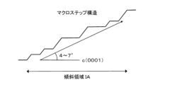
- FIG. 4 schematically shows, for example, a stepped structure (macrostep structure) exposed on the surface of the inclined region IA of one well layer 220.
- the surface of the terrace area TA (terrace T) is not a completely flat surface.
- the single step S1 and the small macro step S2 are clearly distinguished from the large macro step S3, which has a larger number of steps and forms an inclined area IA as shown in FIG.
- the height of the single step S1 and the height of one step of the small macro step S2 and the large macro step S3 of the inclined area IA are 1 ML.
- two or more stages may appear to be one stage in succession.
- Figure 6 shows the cross-sectional profile of the well layer surface measured with an AFM (Atomic Force Microscope) device.
- the units of numerical values shown on the horizontal and vertical axes are nanometers (nm).
- the horizontal axis is set to be parallel to the terrace surface, it is not perfectly aligned, and in the places shown in Figure 6, the terrace surface slopes slightly upward to the right on average with respect to the horizontal axis. It is a face.
- the existence of a large macro step S3 of about 5 to 6 steps corresponding to the slope area IA, a small macro step S2 of about 2 steps, and a single step S1 is confirmed.
- the slope area IA slopes downward to the right, whereas in the schematic diagrams of FIGS. 2 to 5, the slope is tilted upward to the right, with the left and right sides reversed. This is an above difference, not a substantive difference.
- the AlN mole fraction is reduced to the average AlN mole fraction in the well layer 220.
- a Ga-enriched well region 220a lower than Xwa is formed in the inclined region IA.
- the Ga-enriched well region 220a may also be formed in a single step S1 and a small macro step S2 within the terrace region TA.
- the density of Al increases relatively in a part of the terrace region TA.
- an Al-enriched well region is formed in which the AlN mole fraction is higher than the average AlN mole fraction Xwa.
- the average AlN mole fraction Xwa of the well layer 220 is set to 0.21 to 0.25 so that the peak emission wavelength of the EL spectrum of ultraviolet light emission from the active layer 22 is within the range of 300 nm to 320 nm. It is preferably set within a range of 0.22 or more and less than 0.25.
- metastable AlGaN Al 2/12 Ga 10/12 N having an AlN mole fraction lower than the average AlN mole fraction Xwa is formed in the Ga-enriched well region 220a, and further , metastable AlGaN Al 3/12 Ga 9/12 N is formed in the Al-enriched well region, the AlN mole fraction being higher than the average AlN mole fraction Xwa.
- the metastable AlGaN (Al 3/12 Ga 9/12 N) formed in the Al-enriched well region will be referred to as the first metastable AlGaN and the metastable AlGaN formed in the Ga-enriched well region 220a.
- Al 2/12 Ga 10/12 N are respectively referred to as second metastable AlGaN.
- the film thickness of the well layer 220 is such that the average film thickness is within the range of 2.0 nm or more and 3.5 nm or less, and the peak emission wavelength of the EL spectrum of ultraviolet light emission from the active layer 22 is within the range of 300 nm to 320 nm.
- the Al-enriched well region in the terrace region TA is adjusted such that the peak wavelength (first wavelength) of light emission (first light emission) from the first metastable AlGaN is also within the range of 300 nm to 320 nm.
- the film thickness is controlled within a predetermined range.
- the light emission from the first metastable AlGaN (first light emission) and the light emission from the second metastable AlGaN (second light emission) coexist.
- the first light emission needs to be more dominant than the second light emission.
- the EL intensity (first peak EL intensity) of the first emission at the peak wavelength (first wavelength) of the first emission is higher than that of the second emission at the peak wavelength (second wavelength) of the second emission. It needs to be larger than the EL intensity (second peak EL intensity).
- first and second peak EL intensities and the film thickness of the well layer 220 will be discussed in detail in the "EL spectrum of light emitting element" section below.
- a Ga-enriched barrier region 221a is formed in the inclined region IA, the AlN mole fraction being lower than the average AlN mole fraction Xba of the barrier layer 221. Furthermore, an Al-enriched barrier region in which the AlN mole fraction is higher than the average AlN mole fraction Xba of the barrier layer 221 may be formed in a part of the terrace region TA.
- the average AlN mole fraction Xba of the barrier layer 221 is set, for example, within the range of approximately 51% to 90%. Further, the thickness of the barrier layer 221, including the terrace area TA and the slope area IA, is set within a range of, for example, 6 nm to 8 nm.
- the electron block layer 23 similarly to the well layer 220, the electron block layer 23 includes a Ga-enriched EB region 23a in the inclined region IA, the AlN mole fraction of which is lower than the average AlN mole fraction Xea of the electron block layer 23. Further, an Al-enriched EB region having an AlN mole fraction higher than the average AlN mole fraction Xea of the electron block layer 23 may be formed in a part of the terrace region TA.
- the average AlN mole fraction Xea of the electron block layer 23 is set, for example, within the range of approximately 60% to 90%. Further, the film thickness of the electron block layer 23, including the terrace area TA and the inclined area IA, is set within a range of, for example, 15 nm to 30 nm.
- the average AlN mole fractions Xna, Xba, and Xea of the n-type cladding layer 21, the barrier layer 221, and the electron block layer 23 are the same as the average AlN mole fraction Xwa of the well layer 220. This is the target value of the AlN mole fraction at the time of forming each of the layer 221 and the electron block layer 23 or a value close to the target value.
- the p-electrode 26 is made of a multilayer metal film such as Ni/Au, and is formed on the upper surface of the p-type contact layer 24.
- the n-electrode 27 is made of a multilayer metal film such as Ti/Al/Ti/Au, and is formed in a part of the exposed surface of the second region R2 of the n-type cladding layer 21. Note that the p-electrode 26 and the n-electrode 27 are not limited to the above-described multilayer metal film, and the electrode structure such as the metal constituting each electrode, the number of laminated layers, and the laminated order may be changed as appropriate. FIG.
- FIG. 7 shows an example of the shapes of the p-electrode 26 and the n-electrode 27 when viewed from above the light emitting element 1.
- a line BL existing between the p-electrode 26 and the n-electrode 27 indicates the boundary line between the first region R1 and the second region R2. It coincides with the outer peripheral side wall surface of the contact layer 24 .
- the first region R1 and the p-electrode 26 have a comb-like shape in plan view, as an example, but the first region R1 and the p-electrode 26 have a comb-like shape in plan view.
- the visual shape, arrangement, etc. are not limited to the example shown in FIG.
- the AlN layer 12 contained in the base portion 10 and the nitride semiconductor layers 21 to 24 contained in the light emitting element structure portion 20 are epitaxially grown in order on the sapphire substrate 11 by metal organic compound vapor phase epitaxy (MOVPE) method. Layer them together.
- MOVPE metal organic compound vapor phase epitaxy
- the n-type cladding layer 21 is doped with, for example, Si as a donor impurity
- the electron block layer 23 and the p-type contact layer 24 are doped with, for example, Mg as an acceptor impurity.
- At least the surfaces of the AlN layer 12, the n-type cladding layer 21, the active layer 22 (well layer 220, barrier layer 221), and the electron block layer 23 are provided with multi-step terraces parallel to the (0001) plane.
- a slightly inclined substrate is used which is inclined in the m-axis direction or the a-axis direction and has multi-step terraces exposed on the main surface 11a.
- Conditions for such epitaxial growth include, in addition to the use of the (0001) sapphire substrate 11, which is a slightly inclined substrate, as well as a growth rate at which multi-tiered terraces are easily exposed (specifically, for example, growth temperature, source gas, carrier
- the growth rate can be achieved by appropriately setting conditions such as gas supply amount and flow rate. Note that these conditions may differ depending on the type and structure of the film forming apparatus, so it is sufficient to actually produce several samples in the film forming apparatus and specify these conditions.
- the supply amount and flow rate of the raw material gas (trimethylaluminum (TMA) gas, trimethylgallium (TMG) gas, ammonia gas) and carrier gas used in the organometallic compound vapor phase growth method are included in the above-mentioned light emitting element structure section 20.
- the average AlN mole fraction of each of the nitride semiconductor layers 21 to 24 (n-type cladding layer 21: Xna, well layer 220: Xwa, barrier layer 221: Xba, electron block layer 23: Xea) is set as a target value. .
- the optimal values of the growth rate (nm/h) and V/III ratio (supply ratio of Group V element raw material gas and Group III element raw material gas) for the nitride semiconductor layers 21 to 24 may differ for each layer.
- the average AlN mole fraction and preferred range of film thickness for each of the nitride semiconductor layers 21 to 24 have been described above in the section of "Element structure of light emitting element", so a duplicate description will be omitted.
- the growth starting point of the layered region 21a is formed by mass movement of Ga in the step portion (slanted region) between the multi-step terraces formed on the upper surface of the AlN layer 12.
- the growth temperature, growth pressure, and donor impurity concentration are adjusted so that the layered region 21a can grow obliquely upward due to segregation accompanying the mass movement of Ga as the n-type cladding layer 21 is epitaxially grown. selected.
- the growth temperature is preferably 1050° C. or higher, where Ga mass transfer easily occurs, and 1150° C. or lower, where good n-type AlGaN can be prepared.
- the growth pressure 75 Torr or less is preferable as a good AlGaN growth condition, and 10 Torr or more is realistic and preferable as the control limit of the film forming apparatus.
- the donor impurity concentration is preferably about 1 ⁇ 10 18 to 5 ⁇ 10 18 cm ⁇ 3 . Further, the donor impurity concentration does not necessarily need to be controlled uniformly in the vertical direction with respect to the thickness of the n-type cladding layer 21. Note that the above-mentioned growth temperature, growth pressure, etc. are merely examples, and the optimum conditions may be determined as appropriate depending on the film forming apparatus used.
- the entire upper surface of the n-type cladding layer 21 is coated by metal organic compound vapor phase epitaxy (MOVPE), etc.
- MOVPE metal organic compound vapor phase epitaxy
- the active layer 22 well layer 220, barrier layer 221), electron block layer 23, p-type contact layer 24, etc. are formed by the well-known epitaxial growth method.
- the acceptor impurity concentration of the electron block layer 23 is preferably about 1.0 ⁇ 10 16 to 1.0 ⁇ 10 18 cm ⁇ 3 , for example, and the acceptor impurity concentration of the p-type contact layer 24 is, for example, 1.0 About ⁇ 10 18 to 1.0 ⁇ 10 20 cm ⁇ 3 is preferable. Further, the acceptor impurity concentration does not necessarily need to be controlled uniformly in the vertical direction with respect to each film thickness of the electron block layer 23 and the p-type contact layer 24.
- the average AlN mole fraction Xwa of the well layer 220 is set to a target value under growth conditions that facilitate the exposure of the multi-tiered terraces described above.
- the well layer 220 is grown, and the barrier layer 221 is further grown with the average AlN mole fraction Xba of the barrier layer 221 set as a target value.
- the average AlN mole fraction Xwa of the well layer 220 is set within the range of 0.21 or more and less than 0.25, and as the mass of Ga moves, the Ga-enriched well region 220a, a second metastable AlGaN (Al 2/12 Ga 10/12 N) is formed whose AlN mole fraction is lower than the average AlN mole fraction A first metastable AlGaN (Al 3/12 Ga 9/12 N) with a mole fraction higher than Xwa is formed.
- the first emission from the first metastable AlGaN is more dominant than the second emission from the second metastable AlGaN, as described above.
- the upper limit of the off-angle of the sapphire substrate 11 is limited to about 1°, and furthermore, in order to prevent the second emission from becoming more dominant than the first emission, the second metastable AlGaN
- the electron block layer 23 is formed in the same manner as the n-type cladding layer 21, under growth conditions that facilitate the exposure of the multi-tiered terraces described above, with the average AlN mole fraction Xea of the electron block layer 23 set to a target value. Grow layer 23.
- the second region R2 of the nitride semiconductor layers 21 to 24 is selectively etched using a well-known etching method such as reactive ion etching until the upper surface of the n-type cladding layer 21 is exposed. The second region R2 portion of the upper surface is exposed.
- a p-electrode 26 is formed on the p-type contact layer 24 in the unetched first region R1, and an n-type contact layer 26 is formed in the etched first region R2.
- An n-electrode 27 is formed on the mold cladding layer 21. Note that after forming one or both of the p-electrode 26 and the n-electrode 27, heat treatment may be performed using a well-known heat treatment method such as RTA (instant thermal annealing).
- the light emitting element 1 is, for example, flip-chip mounted on a base such as a submount, and then sealed with a predetermined resin (for example, lens-shaped resin) such as silicone resin or amorphous fluororesin. Can be used in any state.
- a predetermined resin for example, lens-shaped resin
- silicone resin or amorphous fluororesin.
- a single step S1, a small macro step S2, and a large macro step S3 are formed in the terrace region TA and slope region IA of the well layer 220, and the surface of the well layer 220 is formed with a single step S1, a small macro step S2, and a large macro step S3.
- FIG. 5 As an example, as schematically shown in FIG.
- the film thickness tT1 There may be a film thickness tT0 of (m-1) ML that is 1 ML thinner.
- m is an integer within the range of 8 to 14.
- the film thickness tS1 is There may be a film thickness tS0 of ML that is 1 ML thinner (m+k-1), a film thickness tS2 of (m+k+1) ML that is 1 ML thicker than film thickness tS1, and a film thickness tS3 of ML that is 2 ML thicker than film thickness tS1 (m+k+2).
- k is an integer greater than or equal to 0, and tends to increase as the mass transfer of Ga increases. In one embodiment, k is assumed to be approximately 1 to 4.
- the EL spectrum of the ultraviolet light emitted from the active layer 22 is a composite spectrum of the EL spectrum of the first light emission (ELS1) and the EL spectrum of the second light emission (ELS2).
- the emission from the main film thickness tT1 of the Al-enriched well region is dominant.
- the peak emission wavelength ⁇ (3, m) of the EL spectrum of the film thickness tT1 (mML) does not necessarily match the peak emission wavelength (first wavelength, ⁇ 1) of the EL spectrum of the first emission (ELS1), and the offset of ⁇ 3 may occur.
- the offset ⁇ 3 changes from die to die of the light emitting element 1 within the wafer due to variations within the wafer, such as the thickness of the well layer 220 and the degree of mass transfer of Ga.
- the emission from the main thickness tS1 of the Ga-enriched well region 220a is dominant.
- the peak emission wavelength ⁇ (2, m+k) of the EL spectrum of the film thickness tS1 ((m+k)ML) does not necessarily match the peak emission wavelength (second wavelength, ⁇ 2) of the EL spectrum (ELS2) of the second emission,
- An offset of ⁇ 2 may occur.
- the offset ⁇ 2 changes from die to die of the light emitting element 1 within the wafer due to variations within the wafer, such as the thickness of the well layer 220 and the degree of mass transfer of Ga.
- the EL spectrum of the first emission (ELS1) and the EL spectrum of the second emission (ELS2) are separated into two peaks, each of which is an independent peak.
- An example is given below.
- the degree of mass movement of Ga within the wafer varies.
- the difference between the peak emission wavelength ⁇ 1 of the first emission and the peak emission wavelength ⁇ 2 of the second emission becomes shorter and the EL intensity of the second emission decreases relative to the first emission, the EL of the second emission decreases.
- the peak of the spectrum does not appear as an independent peak separated from the EL spectrum (ELS1) of the first emission as schematically shown on the left side of FIG. 10, but as shown schematically on the right side of FIG. This may appear as a bulge (shoulder peak) in the emission intensity at the shoulder portion on the long wavelength side of the EL spectrum of the first emission (ELS1).
- an independent peak is defined as a condition where, when the wavelength of the EL spectrum monotonically increases from the wavelength side shorter than the wavelength of the independent peak (peak wavelength), the EL intensity monotonically increases until the wavelength reaches the peak wavelength. It is defined as the peak at the peak wavelength when the wavelength increases, takes a maximum value when the wavelength reaches the peak wavelength, and monotonically decreases as the wavelength increases further beyond the peak wavelength.
- the peak of the EL spectrum (ELS2) of the second emission is equal to the peak of the EL spectrum of the first emission.
- the EL intensity of the EL spectrum of the ultraviolet light emitted from the active layer 22 is expressed as a function with wavelength as a variable, and a plurality of extreme points that take a minimum value in the second derivative of the EL intensity are extracted.
- the first wavelength ⁇ 1 is specified as the wavelength of the extreme value point having the smallest minimum value among the plurality of extreme value points.
- the second wavelength ⁇ 2 is the minimum value of one or more extreme points existing on the longer wavelength side than a reference wavelength that is 10 nm longer than the first wavelength ⁇ 1 selected from the plurality of extreme points. Specified as the wavelength of the value point.
- the identification method even if there are a total of three or more independent peaks and shoulder peaks, the first wavelength ⁇ 1 and the second wavelength ⁇ 2 can be accurately identified. For example, if the EL spectrum has a shoulder peak originating from the first emission at a shorter wavelength or longer wavelength than the first wavelength ⁇ 1, or if there is a small peak due to measurement error in the second derivative of the EL intensity. Even if a value point exists, the wavelength of the shoulder peak or minute extreme point is prevented from being erroneously specified as the second wavelength ⁇ 2.
- a specific example of the first wavelength ⁇ 1 and second wavelength ⁇ 2 according to the identification method will be described later with reference to FIG. 14.
- the first wavelength ⁇ 1 is not determined by the specific method, but is determined by the wavelength at which the EL intensity is the maximum value, or the EL intensity at the zero point among one or more zero points in the first derivative of the EL intensity. It can also be specified as a wavelength.
- the second light emission peak is an independent peak
- the second wavelength ⁇ 2 is also the wavelength of the maximum point where the EL intensity is the maximum value in the wavelength range on the longer wavelength side than the first wavelength ⁇ 1, or the wavelength of the maximum point of the EL It can also be specified as a wavelength at which the EL intensity at the zero point has a maximum value among one or more zero points in the first derivative of intensity.
- each wafer about 40 chips are selected from among the chips with an external quantum efficiency of 0.03% or more along the inflow direction of the raw material gas on the center line of the wafer, and the EL spectra of a total of about 120 chips are obtained. , was measured using an autoprober attached to a spectrometer. The wavelength resolution of the spectrometer used was 0.8 nm.
- the three types of wafers W1, W2, and WR used to measure the EL spectra each have, in order from the bottom, an n-type cladding layer 21, a barrier layer 221, a well layer 220, an AlN layer 223, an electron block layer 23, and a p
- the light emitting device structure 20 shown in FIG. 3 is provided with a type contact layer 24 stacked thereon, and the active layer 22 is a single quantum well structure consisting of one well layer 220 and one barrier layer 221.
- the average AlN mole fraction Xna of the n-type cladding layer 21 is about 45%, and the film thickness is 1.7 ⁇ m.
- the average AlN mole fraction Xba of the barrier layer 221 is about 67%, and the film thickness is about 8 nm.
- the average AlN mole fraction Xnw of the well layer 220 is about 21 to 24%, and the film thickness varies between wafers and within a wafer. It is estimated to be within the range of 2.5 to 3.5 nm based on the growth conditions.
- the thickness of the AlN layer 223 is about 2 nm.
- the average AlN mole fraction Xea of the electron block layer 23 is about 67%, and the film thickness is about 30 nm.
- the p-type contact layer 24 is composed of a p-type GaN layer with a thickness of approximately 25 nm.
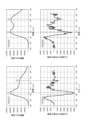
- FIG. 11 shows the distribution state of the peak emission wavelength of each chip (before dicing) in the wafer state of three types of wafers W1, W2, and WR.
- the vertical axis indicates the peak emission wavelength (nm)
- the horizontal axis indicates the position of each chip within the wafer.
- two large and small white circles indicate the peak emission wavelength of the wafer W1
- two large and small black circles indicate the peak emission wavelength of the wafer W1
- an x mark indicates the peak emission wavelength of the wafer WR. From FIG.
- the first emission from the first metastable AlGaN and the second emission from the second metastable AlGaN coexist in the EL spectrum, so the first emission In the case of wafer W1, the first wavelength ⁇ 1, which is the peak wavelength of In the case of wafer W1, the second wavelength ⁇ 2, which is the peak wavelength of the second light emission, falls within the range of 323 nm to 329 nm, excluding the two chips at the edge of the wafer, and in the case of wafer W2, the second wavelength ⁇ 2, which is the peak wavelength of the second light emission, falls within the range of 323 nm to 329 nm, excluding the two chips at the edge of the wafer.
- the wavelength is within the range of 324 nm to 335 nm, except for one chip at each end. Further, the difference between the first wavelength ⁇ 1 and the second wavelength ⁇ 2 is within the range of 17 nm to 26 nm, except for the specific few chips at the wafer edge and the like. Note that the peak at the second wavelength ⁇ 2 of the second light emission includes both an independent peak and a shoulder peak.
- each of the semiconductor layers 21 to 24 of the light emitting element structure 20 has a surface on which multi-step terraces parallel to the (0001) plane are formed.
- the mass transfer of Ga within the well layer 220 does not occur significantly to the extent that the second metastable AlGaN is formed, and as a result, in the EL spectrum of each chip, the 2. No second emission from metastable AlGaN was confirmed. From FIG. 11, it can be seen that in the case of the wafer WR of the comparative example, the first wavelength ⁇ 1, which is the peak wavelength of the first light emission, falls within the range of 301 nm to 311 nm. It is reported in the above-mentioned Non-Patent Document 3 that multi-step terraces parallel to the (0001) plane are not formed in a sapphire substrate with an off-angle of 0.3° or less.
- the off-angle of the sapphire substrate used was only 1.0°, but as the off-angle increased beyond 1.0°, the mass transfer of Ga was further promoted. Therefore, the peak of the second emission from the second metastable AlGaN becomes a prominent independent peak and can be more dominant than the first emission from the first metastable AlGaN. Therefore, the off-angle of the sapphire substrate is 1 It is preferable that the angle is .0° or less.
- the EL intensity at the second wavelength ⁇ 2 of the second light emission from the second metastable AlGaN is equal to the first wavelength of the first light emission from the first metastable AlGaN. Since there are some chips that are larger than the EL intensity at ⁇ 1 (first peak EL intensity), the off-angle of the sapphire substrate is more preferably less than 1.0°, and is 0.9° or less. It is even more preferable.
- the off-angle of the sapphire substrate needs to be larger than 0.3°.
- the AFM image of the surface of the AlN layer formed on the sapphire substrate with an off angle of 0.3° shown in FIG. 2(b) of Non-Patent Document 3, shows that there are hexagonal
- the formation of columnar or hexagonal pyramid-shaped hillocks can be seen, as well as signs of triangular facets, which are traces of step-flow growth that forms multi-tiered terraces.
- FIG. 1 shows that there are hexagonal The formation of columnar or hexagonal pyramid-shaped hillocks can be seen, as well as signs of triangular facets, which are traces of step-flow growth that forms multi-tiered terraces.
- the AFM image of the surface of the AlN layer formed on the sapphire substrate with an off angle of 0.48° shows the multi-step terraces and triangular facets. It can be confirmed that it is clearly formed. Therefore, the lower limit of the off-angle of the sapphire substrate is determined on the condition that multi-step terraces are formed parallel to the (0001) plane, and the value is greater than 0.3° and approximately 0.35° to 0.45°. Estimated to be within a range of °.
- FIG. 12 shows the EL spectra of 3 chips (S11 to S13) of wafer W1 and 6 chips (S21 to S26) of wafer W2 selected from the two types of wafers W1 and W2 of the light emitting element 1 for each wafer.
- the EL spectra of a plurality of chips within the same wafer are displayed overlappingly with their vertical axes shifted so that they are S11 to S13 and S21 to S26 in order from the bottom.
- the vertical axis in FIG. 12 is the normalized EL intensity, and the horizontal axis is the wavelength (nm).
- Table 1 shows the peak emission wavelength (first wavelength, ⁇ 1) of the first emission using the second derivative of the EL intensity for the EL spectra of the nine chips selected from wafers W1 and W2. The results of calculating the peak emission wavelength (second wavelength, ⁇ 2) of the second emission are shown.
- the thickness of the well layer 220 was varied within the range of 6 ML to 15 ML.
- the relaxation rate fR was set to 0.5 in consideration of the device structures and growth conditions of the two types of wafers W1 and W2 of the light emitting device 1.
- the peak emission wavelength of light emission from the first metastable AlGaN ⁇ (3, m) and the peak emission wavelength of light emission from the second metastable AlGaN ⁇ ( 2, m+k) are shown in Tables 3 and 4.
- the film thickness of the Al-enriched well region (mainly the terrace region TA excluding the single step S1 and small macro step S2) of the well layer 220 in which the first metastable AlGaN is formed. It can be seen that for the wafer W1, the distribution is within the range of 9 to 10 ML, and for the wafer W2, it is distributed within the range of 10 to 12 ML. Furthermore, the film thickness of the Ga-enriched well region 220a (mainly the single step S1, small macro step S2, and inclined region IA) of the well layer 220 in which the second metastable AlGaN is formed is 12 to 13 ML in the wafer W1. It can be seen that the distribution is within a range of 12 to 15 ML for wafer W2.
- the average film thickness tARa of the Al-enriched well region 220a and the average film thickness tGRa of the Ga-enriched well region 220a for each chip are determined from the relationship between the peak emission wavelength and film thickness shown in FIG. can be derived as the film thickness corresponding to the second wavelength ⁇ 2. From the results shown in Tables 3 and 4, it can be seen that the average thickness tARa of the Al-enriched well region is smaller than the average thickness tGRa of the Ga-enriched well region 220a.
- the average film thickness of the well layer 220 over the terrace region TA and the slope region IA can be estimated from the growth conditions of the well layer 220, it is difficult to accurately measure it.
- the area of the terrace region TA and the slope region IA shown in the entire well layer 220 is several times larger than the area of the slope region IA, so the average film thickness tQWa of the well layer 220 is
- the average film thickness tARa of the Al-enriched well region is closer to the average film thickness tARa of the Al-enriched well region than the average value tAGa of the average film thickness tARa of the enriched well region and the average film thickness tGRa of the Ga-enriched well region 220a.
- the second derivative of the EL intensity of the EL spectrum of the ultraviolet emission from the active layer 22 described above It is assumed that it has become clear that the first wavelength ⁇ 1 and the second wavelength ⁇ 2 can be calculated using .
- the first light emission from the first metastable AlGaN and the second light emission from the second metastable AlGaN coexist.
- the feature is that the first light emission is more dominant than the second light emission.
- the AlN mole fraction of the AlGaN-based semiconductor constituting the well layer 220 is lower than in a case where the peak emission wavelength is less than about 285 nm.
- the holes that reach the terrace region TA in the well layer 220 are recombined radiatively in the terrace region TA where the mole fraction of AlN is higher than that in the inclined region IA.
- Light emission occurs at a shorter wavelength than the inclined region IA.
- the light emitting element 1 effectively utilizes the emission recombination in the terrace area TA to realize a peak emission wavelength of around 310 nm with high internal quantum efficiency.
- the p-type layer constituting the light-emitting device structure 20 was two layers, the electron block layer 23 and the p-type contact layer 24, but the electron block layer 23 and the p-type A configuration may also be adopted in which one or more p-type cladding layers made of a p-type AlGaN-based semiconductor are provided between the contact layers 24.
- Mg can be used similarly to the electron block layer 23 and the p-type contact layer 24.
- the p-type cladding layer is active with the AlN layer 12 of the base portion 10 and the n-type cladding layer 21 of the light emitting element structure portion 20, which are epitaxially grown in order from the main surface 11a of the sapphire substrate 11.
- the p-type cladding layer is active with the AlN layer 12 of the base portion 10 and the n-type cladding layer 21 of the light emitting element structure portion 20, which are epitaxially grown in order from the main surface 11a of the sapphire substrate 11.
- the p-type cladding layer is active with the AlN layer 12 of the base portion 10 and the n-type cladding layer 21 of the light emitting element structure portion 20, which are epitaxially grown in order from the main surface 11a of the sapphire substrate 11.
- the p-type cladding layer is active with the AlN layer 12 of the base portion 10 and the n-type cladding layer 21 of the light emitting element structure portion 20, which are epitaxially grown in order from the main surface 11
- the average AlN mole fraction of the p-type cladding layer is set within the range of approximately 52% to 74%, and the film thickness is set within the range of 20 nm to 200 nm, for example.
- the supply amount and flow rate of the raw material gas and carrier gas used in the organometallic compound vapor phase epitaxy are such that the n-type cladding layer 21 is formed. It has been explained that it is set according to the average AlN mole fraction of the entire n-type AlGaN layer. In other words, if the average AlN mole fraction of the entire n-type cladding layer 21 is set to a constant value in the vertical direction, it is assumed that the supply amount and flow rate of the raw material gas etc. are controlled to be constant. . However, the supply amount and flow rate of the raw material gas etc. do not necessarily have to be controlled to be constant.
- the first region R1 and the p-electrode 26 have, for example, a comb shape in plan view, but the plan view shape is not limited to the comb shape.
- a plurality of first regions R1 may exist, each surrounded by one second region R2 in a plan view shape.
- the light emitting element 1 includes the base part 10 including the sapphire substrate 11. 10) may be removed by lift-off or the like. Furthermore, the substrate constituting the base portion 10 is not limited to a sapphire substrate.
- the present invention provides a light emitting device structure having a light emitting device structure in which an n-type layer, an active layer, and a p-type layer made of an AlGaN-based semiconductor with a wurtzite structure are stacked in the vertical direction. It can be used in existing nitride semiconductor ultraviolet light emitting devices.
- Nitride semiconductor ultraviolet light emitting device 10 Base portion 11: Sapphire substrate 11a: Main surface of sapphire substrate 12: AlN layer 20: Light emitting device structure portion 21: N-type cladding layer (n-type layer) 21a: Layered region (n-type layer) 21b: n-type main body region (n-type layer) 22: Active layer 220: Well layer 220a: Ga-enriched well region 221: Barrier layer 221a: Ga-enriched barrier region 223: AlN layer 23: Electron blocking layer (p-type layer) 23a: Ga-enriched EB region 24: p-type contact layer (p-type layer) 26: p-electrode 27: n-electrode 100: substrate 101: AlGaN-based semiconductor layer 102: template 103: n-type AlGaN-based semiconductor layer 104: active layer 105: p-type AlGaN-based semiconductor layer 106: p-type contact layer 107: n-electrode 108: P electrode BL
Abstract
Provided is a nitride semiconductor ultraviolet light-emitting diode having a peak emission wavelength in the range of 300-320 nm and comprising a light-emitting diode structure in which an n-type layer, an active layer, and a p-type layer made of AlGaN-based semiconductors are laminated. Each semiconductor layer in the n-type layer, the active layer, and the p-type layer is an epitaxial growth layer having a surface on which multi-stepped terraces parallel to the (0001) plane are formed, the active layer has a quantum well structure including at least one well layer, the average AlN mole fraction in each well layer is in the range of 0.21 or more and less than 0.25, the average film thickness of each well layer is in the range of 2.0-3.5 nm, and a first emission from Al1/4Ga3/4N and a second emission from Al1/6Ga5/6N are mixed in the emission from the at least one well layer. In the EL spectrum of the emission from the active layer, a first wavelength, which is the peak wavelength of the first emission, is shorter than a second wavelength, which is the peak wavelength of the second emission, and the EL intensity at the first wavelength is greater than the EL intensity at the second wavelength.
Description
本発明は、ウルツ鉱構造のAlGaN系半導体からなるn型層、活性層、及びp型層が上下方向に積層された発光素子構造部を備えてなるピーク発光波長が300nm~320nmの範囲内に存在する窒化物半導体紫外線発光素子に関する。
The present invention provides a light emitting device structure having a light emitting device structure in which an n-type layer, an active layer, and a p-type layer made of an AlGaN-based semiconductor with a wurtzite structure are stacked in the vertical direction. This invention relates to existing nitride semiconductor ultraviolet light emitting devices.
一般的に、窒化物半導体発光素子は、サファイア等の基板上にエピタキシャル成長により複数の窒化物半導体層からなる発光素子構造を形成したものが多数存在する。窒化物半導体層は、一般式Al1-x-yGaxInyN(0≦x≦1,0≦y≦1,0≦x+y≦1)で表される。
In general, there are many nitride semiconductor light emitting devices in which a light emitting device structure consisting of a plurality of nitride semiconductor layers is formed by epitaxial growth on a substrate such as sapphire. The nitride semiconductor layer is represented by the general formula Al 1-xy Ga x In y N (0≦x≦1, 0≦y≦1, 0≦x+y≦1).
発光ダイオードの発光素子構造は、n型窒化物半導体層とp型窒化物半導体層の2つのクラッド層の間に、窒化物半導体層よりなる活性層が挟まれたダブルへテロ構造を有している。活性層がAlGaN系半導体の場合、AlNモル分率(Al組成比とも言う)を調整することにより、バンドギャップエネルギを、GaNとAlNが取り得るバンドギャップエネルギ(約3.4eVと約6.2eV)を夫々下限及び上限とする範囲内で調整でき、発光波長が約200nmから約365nmまでの紫外線発光素子が得られる。具体的には、p型窒化物半導体層からn型窒化物半導体層に向けて順方向電流を流すことで、活性層においてキャリア(電子及び正孔)の再結合による上記バンドギャップエネルギに応じた発光が生じる。当該順方向電流を外部から供給するために、p型窒化物半導体層上にp電極が、n型窒化物半導体層上にn電極が、夫々設けられている。
The light emitting element structure of a light emitting diode has a double heterostructure in which an active layer made of a nitride semiconductor layer is sandwiched between two cladding layers, an n-type nitride semiconductor layer and a p-type nitride semiconductor layer. There is. When the active layer is an AlGaN-based semiconductor, by adjusting the AlN mole fraction (also called Al composition ratio), the band gap energy can be changed to the band gap energy that GaN and AlN can take (approximately 3.4 eV and approximately 6.2 eV). ) can be adjusted within the range of the lower limit and upper limit, respectively, and an ultraviolet light emitting device with an emission wavelength of about 200 nm to about 365 nm can be obtained. Specifically, by flowing a forward current from the p-type nitride semiconductor layer to the n-type nitride semiconductor layer, the recombination of carriers (electrons and holes) in the active layer is performed according to the above band gap energy. Luminescence occurs. In order to supply the forward current from the outside, a p-electrode is provided on the p-type nitride semiconductor layer, and an n-electrode is provided on the n-type nitride semiconductor layer.
活性層がAlGaN系半導体の場合、活性層を挟むn型窒化物半導体層とp型窒化物半導体層は、活性層より高AlNモル分率のAlGaN系半導体で構成される。しかし、高AlNモル分率のp型窒化物半導体層は、p電極と良好なオーミック接触を形成することが困難なため、p型窒化物半導体層の最上層に低AlNモル分率のp型AlGaN系半導体(具体的にはp-GaN)からなるp電極と良好なオーミック接触可能なp型コンタクト層を形成することが一般的に行われている。このp型コンタクト層は、AlNモル分率が活性層を構成するAlGaN系半導体より小さいため、活性層からp型窒化物半導体層側に向けて出射された紫外線は該p型コンタクト層で吸収され、素子外部に有効に取り出すことができない。このため、活性層がAlGaN系半導体の一般的な紫外線発光ダイオードは、図15に模式的に示すような素子構造を採用し、活性層からn型窒化物半導体層側に向けて出射された紫外線を素子外部に有効に取り出している(例えば、下記の特許文献1~3等参照)。
When the active layer is an AlGaN-based semiconductor, the n-type nitride semiconductor layer and the p-type nitride semiconductor layer sandwiching the active layer are composed of AlGaN-based semiconductors having a higher AlN mole fraction than the active layer. However, since it is difficult for a p-type nitride semiconductor layer with a high AlN mole fraction to form a good ohmic contact with a p-electrode, a p-type layer with a low AlN mole fraction is added to the top layer of the p-type nitride semiconductor layer. It is common practice to form a p-type contact layer that can make good ohmic contact with a p-electrode made of an AlGaN-based semiconductor (specifically, p-GaN). Since the AlN mole fraction of this p-type contact layer is smaller than that of the AlGaN-based semiconductor constituting the active layer, ultraviolet rays emitted from the active layer toward the p-type nitride semiconductor layer are absorbed by the p-type contact layer. , cannot be effectively taken out to the outside of the device. For this reason, a typical ultraviolet light emitting diode whose active layer is an AlGaN-based semiconductor adopts a device structure as schematically shown in FIG. is effectively taken out to the outside of the device (for example, see Patent Documents 1 to 3 below).
図15に示すように、一般的な紫外線発光ダイオードは、サファイア基板等の基板100上にAlGaN系半導体層101(例えば、AlN層)を堆積して形成されたテンプレート102上に、n型AlGaN系半導体層103、活性層104、p型AlGaN系半導体層105、及び、p型コンタクト層106を順番に堆積し、活性層104とp型AlGaN系半導体層105とp型コンタクト層106の一部を、n型AlGaN系半導体層103が露出するまでエッチング除去し、n型AlGaN系半導体層103の露出面にn電極107を、p型コンタクト層106の表面にp電極108を夫々形成して構成される。
As shown in FIG. 15, a typical ultraviolet light emitting diode has an n-type AlGaN-based semiconductor layer 101 (for example, an AlN layer) deposited on a template 102 formed by depositing an AlGaN-based semiconductor layer 101 (for example, an AlN layer) on a substrate 100 such as a sapphire substrate. A semiconductor layer 103, an active layer 104, a p-type AlGaN-based semiconductor layer 105, and a p-type contact layer 106 are deposited in order, and a part of the active layer 104, p-type AlGaN-based semiconductor layer 105, and p-type contact layer 106 are deposited. , by etching and removing the n-type AlGaN-based semiconductor layer 103 until it is exposed, and forming an n-electrode 107 on the exposed surface of the n-type AlGaN-based semiconductor layer 103 and a p-electrode 108 on the surface of the p-type contact layer 106. Ru.
また、活性層内でのキャリア再結合による発光効率(内部量子効率)を高めるために、活性層を多重量子井戸構造とすること、活性層上に電子ブロック層を設けること等が実施されている。
In addition, in order to increase the luminous efficiency (internal quantum efficiency) due to carrier recombination within the active layer, methods such as forming the active layer into a multi-quantum well structure and providing an electron blocking layer on the active layer have been implemented. .
一方、n型AlGaN系半導体層で構成されるクラッド層内においてGaの偏析(Gaの質量移動に伴う偏析)による組成変調が生じ、クラッド層表面に対して斜め方向に延伸する局所的にAlNモル分率の低い層状領域が形成されることが報告されている(例えば、下記の特許文献4、非特許文献1,2等参照)。局所的にAlNモル分率の低いAlGaN系半導体層はバンドギャップエネルギも局所的に小さくなるため、特許文献4では、当該クラッド層内のキャリアが層状領域に局在化し易くなり、活性層に対して低抵抗の電流経路を提供することができ、紫外線発光ダイオードの発光効率の向上が図れることが報告されている。
On the other hand, within the cladding layer composed of an n-type AlGaN-based semiconductor layer, compositional modulation occurs due to Ga segregation (segregation due to mass movement of Ga), and local AlN moles extending obliquely to the cladding layer surface occur. It has been reported that a layered region with a low fraction is formed (for example, see Patent Document 4, Non-Patent Documents 1 and 2, etc. below). Since the band gap energy of an AlGaN-based semiconductor layer with a locally low AlN mole fraction is locally small, in Patent Document 4, carriers in the cladding layer are likely to be localized in the layered region, and the active layer is It has been reported that ultraviolet light can provide a low-resistance current path and improve the luminous efficiency of ultraviolet light-emitting diodes.
更に、n型クラッド層上に形成される多重量子井戸構造の活性層の各層の表面に(0001)面に平行な多段状のテラスが表出し、n型クラッド層と同様に、活性層の各層内でGaの偏析による組成変調が生じ、隣接するテラス間を連結する(0001)面に対して傾斜した傾斜領域に、相対的にAlNモル分率の低い領域が生成され、テラス領域に、相対的にAlNモル分率の高い領域が生成され、ピーク発光波長の異なる傾斜領域からの発光とテラス領域からの発光が合成される結果、活性層全体のEL(エレクトロルミネセンス)スペクトルにおいて複数ピークの重なりの生じ得ることが、非特許文献1で報告されている。
Furthermore, multi-tiered terraces parallel to the (0001) plane are exposed on the surface of each layer of the active layer of the multi-quantum well structure formed on the n-type cladding layer, and each layer of the active layer is formed on the n-type cladding layer. As a result, a region with a relatively low AlN mole fraction is generated in a slope region that is inclined with respect to the (0001) plane connecting adjacent terraces, and a region with a relatively low AlN mole fraction is generated in the terrace region. As a result, a region with a high AlN mole fraction is generated, and the light emission from the slope region and the terrace region with different peak emission wavelengths are combined, resulting in multiple peaks in the EL (electroluminescence) spectrum of the entire active layer. It is reported in Non-Patent Document 1 that overlap may occur.
また、下記の特許文献1には、上記Gaの偏析に伴う発光波長分布の広がり(半値全幅)は、発光波長が長い程大きくなる傾向があることが記載されている。更に、特許文献1の図13には、井戸層を構成するAlGaN層のAlNモル分率が35%でオフ角が0.15°、0.3°、1°の3つのサンプルのELスペクトルが開示されており、オフ角が0.15°、0.3°、1°と大きくなるに伴い、上記Gaの偏析が顕著となり、ピーク発光波長が約289nm~約299nmの範囲で順次長くなるとともに、オフ角が0.3°を超えると発光波長分布の広がりが極端に広がることが分かる。
Further, Patent Document 1 below describes that the spread of the emission wavelength distribution (full width at half maximum) due to the segregation of Ga tends to increase as the emission wavelength becomes longer. Furthermore, FIG. 13 of Patent Document 1 shows the EL spectra of three samples in which the AlN mole fraction of the AlGaN layer constituting the well layer is 35% and the off angles are 0.15°, 0.3°, and 1°. As the off-angle increases to 0.15°, 0.3°, and 1°, the segregation of Ga becomes significant, and the peak emission wavelength becomes sequentially longer in the range of about 289 nm to about 299 nm. , it can be seen that when the off-angle exceeds 0.3°, the spread of the emission wavelength distribution becomes extremely wide.
また、下記の特許文献5及び6には、AlNモル分率がn/12(但し、nは1~11の整数)で表されるAln/12Ga1-n/12N(AlnGa12-nN12とも表記できる)が、AlNモル分率がn/12以外のAlGaNより安定的に形成されることが報告されている。また、当該Aln/12Ga1-n/12Nは、特許文献5及び6において「準安定AlGaN」と名付けられており、本明細書でもそのように呼称する。ここで、Gaの偏析によりn型クラッド層内に形成される局所的にAlNモル分率の低い層状領域、及び、井戸層の傾斜領域に形成される局所的にAlNモル分率の低い領域に、上記準安定AlGaNを安定的に形成することで、結晶成長装置のドリフト等に起因する特性変動の抑制された窒化物半導体紫外線発光素子を提供できることが報告されている。
Further, in Patent Documents 5 and 6 below, Al n/12 Ga 1-n/12 N (Al n Ga It has been reported that 12-n N 12 ) is formed more stably than AlGaN with an AlN molar fraction other than n/12. Further, the Al n/12 Ga 1-n/12 N is named "metastable AlGaN" in Patent Documents 5 and 6, and is also referred to as such in this specification. Here, a layered region with a locally low AlN mole fraction formed in the n-type cladding layer due to Ga segregation, and a locally low AlN mole fraction region formed in the inclined region of the well layer. It has been reported that by stably forming the above-mentioned metastable AlGaN, it is possible to provide a nitride semiconductor ultraviolet light emitting device in which characteristic fluctuations caused by drift of a crystal growth apparatus are suppressed.
上記特許文献5及び6に開示されている窒化物半導体紫外線発光素子では、上記特許文献4、非特許文献1,2に開示されているように、n型クラッド層内にGaの偏析によって形成される局所的にAlNモル分率の低いAlGaN系半導体層の層状領域を、井戸層の傾斜領域にGaの偏析によって同様に形成される相対的にAlNモル分率の低い領域に対して集中的に電流を供給する低抵抗の電流経路とし、更に、当該傾斜領域に上記準安定AlGaNを安定的に形成することで、紫外線発光ダイオードの発光効率の向上と結晶成長装置のドリフト等に起因する特性変動の抑制の両立が図られている。
In the nitride semiconductor ultraviolet light emitting devices disclosed in Patent Documents 5 and 6, as disclosed in Patent Document 4 and Non-Patent Documents 1 and 2, Ga is formed in the n-type cladding layer by segregation. The layered region of the AlGaN-based semiconductor layer with a locally low AlN mole fraction is intensively applied to the region with a relatively low AlN mole fraction that is similarly formed by segregation of Ga in the inclined region of the well layer. By creating a low-resistance current path for supplying current and stably forming the above-mentioned metastable AlGaN in the slope region, the luminous efficiency of the ultraviolet light emitting diode can be improved and characteristic fluctuations caused by crystal growth equipment drift etc. The aim is to simultaneously suppress the
しかし、上記特許文献5及び6では、準安定AlGaNのAlNモル分率n/12の整数nが1~3と小さい場合、つまり、Gaの組成比が大きい準安定AlGaNでは、1000℃付近の成長温度において、Gaの質量移動が激しく原子配列の対称性が乱れ、AlとGaの原子配列はランダムな状態に近くなり、安定度が他の準安定AlGaNと比べて低下すると考えられていたため、井戸層の傾斜領域に形成される準安定AlGaNのAlNモル分率n/12の整数nとして4以上が想定されていた。この場合、井戸層からの発光は、AlNモル分率n/12の準安定AlGaNが形成されている傾斜領域からの発光が支配的となる。整数n=4の準安定AlGaNの場合、井戸層の傾斜領域の膜厚を5~14ML(単原子層(monolayer))の範囲内で設定すると、一例として、ピーク発光波長は277~315nmの範囲内に制御し得る。
However, in Patent Documents 5 and 6, when the integer n of the AlN molar fraction n/12 of metastable AlGaN is as small as 1 to 3, that is, in metastable AlGaN with a large composition ratio of Ga, the growth rate is around 1000°C. At high temperatures, the mass transfer of Ga is intense and the symmetry of the atomic arrangement is disturbed, and the atomic arrangement of Al and Ga becomes nearly random, which is thought to reduce the stability compared to other metastable AlGaN. It was assumed that the integer n of the AlN mole fraction n/12 of the metastable AlGaN formed in the inclined region of the layer was 4 or more. In this case, the light emission from the well layer is dominated by the light emission from the inclined region where metastable AlGaN with an AlN molar fraction of n/12 is formed. In the case of metastable AlGaN with an integer n = 4, if the thickness of the inclined region of the well layer is set within the range of 5 to 14 ML (monolayer), the peak emission wavelength will be in the range of 277 to 315 nm, for example. can be controlled within
アトピー性皮膚炎の紫外線治療、UVインクの硬化等に有用なピーク発光波長が310nm付近にある紫外線発光を、整数n=4の準安定AlGaNを井戸層の傾斜領域に形成して実現するには、理論上は、傾斜領域の膜厚を14ML程度まで厚くすれば良い。しかしながら、一般的に、井戸層の膜厚を3.5nm(約13.6ML)以上に厚くすると安定した発光が得られ難くなるという問題がある。
How to achieve ultraviolet light emission with a peak emission wavelength around 310 nm, which is useful for ultraviolet treatment of atopic dermatitis, curing of UV ink, etc., by forming metastable AlGaN with an integer n = 4 in the inclined region of the well layer. Theoretically, it is sufficient to increase the film thickness of the inclined region to about 14 ML. However, in general, there is a problem that when the thickness of the well layer is increased to 3.5 nm (approximately 13.6 ML) or more, it becomes difficult to obtain stable light emission.
量子井戸構造の井戸層からのピーク発光波長は、井戸層のAlNモル分率と膜厚に応じて変化するが、更に、井戸層内における活性層の下方側に形成されるn型AlGaN層及び更に下方側のAlN層等から受ける(0001)面に平行な方向の応力等の影響により変動する。従って、ピーク発光波長は、後述のバリア層に対する緩和率(fR)をパラメータとする井戸層のAlNモル分率と膜厚の関数として与えられる。ここで、緩和率fRは、当該応力の影響を示す指標として、バリア層及びn型AlGaN層の格子定数つまりAlNモル分率の関数として与えられ、ピーク発光波長を井戸層のAlNモル分率と膜厚の関数として表現する場合のフィッティング・パラメータとして機能する。
The peak emission wavelength from the well layer of the quantum well structure varies depending on the AlN mole fraction and film thickness of the well layer. Furthermore, it fluctuates due to the influence of stress in the direction parallel to the (0001) plane, etc., which is received from the lower AlN layer, etc. Therefore, the peak emission wavelength is given as a function of the AlN mole fraction and film thickness of the well layer with the relaxation rate (f R ) for the barrier layer as described later as a parameter. Here, the relaxation rate f R is given as a function of the lattice constant of the barrier layer and the n-type AlGaN layer, that is, the AlN mole fraction, as an index indicating the influence of the stress, and the peak emission wavelength is determined by the AlN mole fraction of the well layer. functions as a fitting parameter when expressed as a function of film thickness.
更に、緩和率fRの違いによるピーク発光波長の変動幅は、井戸層の膜厚が10MLを超えて14MLに向けて大きくなるほど大きくなる傾向がある。また、ピーク発光波長が300nm以上の波長範囲では、活性層の下方側に形成されるn型AlGaN層のAlNモル分率を60%程度以下に抑えることが好ましいという事情がある。更に、後述するように、活性層の各層の表面に表出する(0001)面に平行な多段状のテラスの表面上にも、傾斜領域に比べて段数の少ない1段(1段の高さは1ML)また2段程度の微小な段差が生じており、1素子の井戸層全体での膜厚の変動が2MLを超える場合がある。
Furthermore, the fluctuation width of the peak emission wavelength due to the difference in the relaxation rate f R tends to increase as the thickness of the well layer increases from more than 10 ML toward 14 ML. Further, in a wavelength range where the peak emission wavelength is 300 nm or more, it is preferable to suppress the AlN mole fraction of the n-type AlGaN layer formed below the active layer to about 60% or less. Furthermore, as will be described later, on the surface of the multi-step terrace parallel to the (0001) plane exposed on the surface of each layer of the active layer, there is also a single step (one step high), which has a smaller number of steps than the inclined region. (1 ML) Also, a minute step difference of about two steps occurs, and the variation in film thickness of the entire well layer of one element may exceed 2 ML.
従って、井戸層の傾斜領域の膜厚を14ML程度まで厚くし、整数n=4の準安定AlGaNを井戸層の傾斜領域に形成できるようにしても、ピーク発光波長が310nm付近の紫外線発光を安定的に実現するのは、現実的には困難である。
Therefore, even if the film thickness of the inclined region of the well layer is increased to about 14 ML and metastable AlGaN with an integer n = 4 can be formed in the inclined region of the well layer, ultraviolet light emission with a peak emission wavelength of around 310 nm will be stabilized. In reality, it is difficult to achieve this objective.
本発明は、上述の問題点に鑑みてなされたものであり、その目的は、ピーク発光波長が310nm付近の窒化物半導体紫外線発光素子を安定して提供することにある。
The present invention has been made in view of the above-mentioned problems, and its purpose is to stably provide a nitride semiconductor ultraviolet light emitting device with a peak emission wavelength of around 310 nm.
本願発明者は、鋭意研究により、整数nが4以上の準安定AlGaN(Aln/12Ga1-n/12N)に比べて安定度が低いと考えられていた整数nが3及び2のAl3/12Ga9/12NとAl2/12Ga10/12Nも、準安定AlGaNとして井戸層内に安定的に形成され得ることを、複数のウェハ上の多数のダイからのELスペクトルに対して統計的に分析を行って確認し、更に、整数nが2及び3の2種類の準安定AlGaNを、前者を井戸層の傾斜領域に、後者をテラス領域に形成することにより、テラス領域からの発光を有効に利用して、ピーク発光波長が310nm付近の窒化物半導体紫外線発光素子を安定して作製し得ることを確認し、以下に詳細に説明する本発明に至った。尚、上記統計的分析の内容については、本願における「不利にならない開示又は新規性喪失の例外に関する申立て」の対象としている下記の2022年3月29日公開の刊行物に詳細に開示されており、また、Al3/12Ga9/12NとAl2/12Ga10/12Nが、整数nが4以上の準安定AlGaN(Aln/12Ga1-n/12N)に比べて安定度が低下するものの、準安定AlGaNとして機能し得ることは上記特許文献5及び6に開示されているので、本願明細書では重複する説明は省略する。
[刊行物]
Y. Nagasawa, et al., "Dual-peak electroluminescence spectra generated from Aln/12Ga1-n/12N (n = 2, 3, 4) for AlGaN-based LEDs with nonflat quantum wells", Journal of Physics D: Applied Physics 55 (2022) 255102 Through intensive research, the inventor of the present application discovered that the stability of AlGaN with an integer n of 3 and 2, which was considered to be less stable than metastable AlGaN with an integer n of 4 or more (Al n/12 Ga 1-n/12 N), EL spectra from multiple dies on multiple wafers show that Al 3/12 Ga 9/12 N and Al 2/12 Ga 10/12 N can also be stably formed in the well layer as metastable AlGaN. This was confirmed through statistical analysis, and further, by forming two types of metastable AlGaN with an integer n of 2 and 3, the former in the slope region of the well layer and the latter in the terrace region, the terrace It was confirmed that a nitride semiconductor ultraviolet light emitting device with a peak emission wavelength of around 310 nm could be stably produced by effectively utilizing light emitted from the region, and the present invention, which will be described in detail below, was achieved. The content of the above statistical analysis is disclosed in detail in the following publication published on March 29, 2022, which is the subject of the "petition regarding non-prejudicial disclosure or exception to loss of novelty" in this application. In addition, Al 3/12 Ga 9/12 N and Al 2/12 Ga 10/12 N are smaller than metastable AlGaN (Al n/12 Ga 1-n/12 N) where the integer n is 4 or more. Although the stability is lowered, it is disclosed inPatent Documents 5 and 6 that it can function as metastable AlGaN, so a redundant explanation will be omitted in this specification.
[Publications]
Y. Nagasawa, et al., "Dual-peak electroluminescence spectra generated from Al n/12 Ga 1-n/12 N (n = 2, 3, 4) for AlGaN-based LEDs with nonflat quantum wells", Journal of Physics D: Applied Physics 55 (2022) 255102
[刊行物]
Y. Nagasawa, et al., "Dual-peak electroluminescence spectra generated from Aln/12Ga1-n/12N (n = 2, 3, 4) for AlGaN-based LEDs with nonflat quantum wells", Journal of Physics D: Applied Physics 55 (2022) 255102 Through intensive research, the inventor of the present application discovered that the stability of AlGaN with an integer n of 3 and 2, which was considered to be less stable than metastable AlGaN with an integer n of 4 or more (Al n/12 Ga 1-n/12 N), EL spectra from multiple dies on multiple wafers show that Al 3/12 Ga 9/12 N and Al 2/12 Ga 10/12 N can also be stably formed in the well layer as metastable AlGaN. This was confirmed through statistical analysis, and further, by forming two types of metastable AlGaN with an integer n of 2 and 3, the former in the slope region of the well layer and the latter in the terrace region, the terrace It was confirmed that a nitride semiconductor ultraviolet light emitting device with a peak emission wavelength of around 310 nm could be stably produced by effectively utilizing light emitted from the region, and the present invention, which will be described in detail below, was achieved. The content of the above statistical analysis is disclosed in detail in the following publication published on March 29, 2022, which is the subject of the "petition regarding non-prejudicial disclosure or exception to loss of novelty" in this application. In addition, Al 3/12 Ga 9/12 N and Al 2/12 Ga 10/12 N are smaller than metastable AlGaN (Al n/12 Ga 1-n/12 N) where the integer n is 4 or more. Although the stability is lowered, it is disclosed in
[Publications]
Y. Nagasawa, et al., "Dual-peak electroluminescence spectra generated from Al n/12 Ga 1-n/12 N (n = 2, 3, 4) for AlGaN-based LEDs with nonflat quantum wells", Journal of Physics D: Applied Physics 55 (2022) 255102
本発明は、上記目的を達成するために、ピーク発光波長が300nm~320nmの範囲内に存在する窒化物半導体紫外線発光素子であって、
n型AlGaN系半導体で構成されたn型層、AlGaN系半導体で構成された活性層、及び、p型AlGaN系半導体で構成されたp型層が上下方向に積層された発光素子構造部を備え、
前記n型層と前記活性層と前記p型層内の各半導体層が、(0001)面に平行な多段状のテラスが形成された表面を有するエピタキシャル成長層であり、
前記活性層が1層以上の井戸層を含む量子井戸構造を有し、
前記1層以上の井戸層の各井戸層の平均AlNモル分率が、0.21以上0.25未満の範囲内にあり、
前記各井戸層の平均膜厚が2.0nm以上3.5nm以下の範囲内にあり、
前記1層以上の井戸層からの発光に、Al1/4Ga3/4Nからの第1発光とAl1/6Ga5/6Nからの第2発光が混在しており、
前記窒化物半導体紫外線発光素子のELスペクトルにおいて、前記第1発光のピーク波長である第1波長が、前記第2発光のピーク波長である第2波長より短く、前記第1波長おけるEL強度が前記第2波長におけるEL強度より大きいことを特徴とする窒化物半導体紫外線発光素子を提供する。 In order to achieve the above object, the present invention provides a nitride semiconductor ultraviolet light emitting device having a peak emission wavelength within a range of 300 nm to 320 nm,
A light emitting element structure in which an n-type layer made of an n-type AlGaN-based semiconductor, an active layer made of an AlGaN-based semiconductor, and a p-type layer made of a p-type AlGaN-based semiconductor are stacked in the vertical direction. ,
Each semiconductor layer in the n-type layer, the active layer, and the p-type layer is an epitaxially grown layer having a surface on which multi-step terraces parallel to the (0001) plane are formed;
The active layer has a quantum well structure including one or more well layers,
The average AlN mole fraction of each well layer of the one or more well layers is within a range of 0.21 or more and less than 0.25,
The average film thickness of each well layer is within a range of 2.0 nm or more and 3.5 nm or less,
The light emission from the one or more well layers includes a first light emission from Al 1/4 Ga 3/4 N and a second light emission from Al 1/6 Ga 5/6 N,
In the EL spectrum of the nitride semiconductor ultraviolet light emitting device, the first wavelength that is the peak wavelength of the first emission is shorter than the second wavelength that is the peak wavelength of the second emission, and the EL intensity at the first wavelength is Provided is a nitride semiconductor ultraviolet light emitting device characterized by having an EL intensity greater than that at a second wavelength.
尚、AlGaN系半導体とは、一般式Al1-xGaxN(0≦x≦1)で表されるが、バンドギャップエネルギがGaNとAlNが取り得るバンドギャップエネルギを夫々下限及び上限とする範囲内であれば、BまたはIn等の3族元素またはP等の5族元素等の不純物を微量に含んでいてもよい。また、GaN系半導体とは、基本的にGaとNで構成される窒化物半導体であるが、Al、BまたはIn等の3族元素またはP等の5族元素等の不純物を微量に含んでいてもよい。また、AlN系半導体とは、基本的にAlとNで構成される窒化物半導体であるが、Ga、BまたはIn等の3族元素またはP等の5族元素等の不純物を微量に含んでいてもよい。従って、本願では、GaN系半導体及びAlN系半導体は、それぞれAlGaN系半導体の一部である。
Incidentally, an AlGaN-based semiconductor is represented by the general formula Al 1-x Ga x N (0≦x≦1), and the band gap energy is set to the lower and upper limits of the band gap energy that GaN and AlN can take, respectively. As long as it is within the range, a trace amount of impurity such as a group 3 element such as B or In or a group 5 element such as P may be included. GaN-based semiconductors are basically nitride semiconductors composed of Ga and N, but they also contain trace amounts of impurities such as group 3 elements such as Al, B, or In, or group 5 elements such as P. You can stay there. In addition, an AlN-based semiconductor is a nitride semiconductor basically composed of Al and N, but it also contains trace amounts of impurities such as group 3 elements such as Ga, B, or In, or group 5 elements such as P. You can stay there. Therefore, in this application, the GaN-based semiconductor and the AlN-based semiconductor are each part of the AlGaN-based semiconductor.
更に、n型またはp型AlGaN系半導体は、ドナーまたはアクセプタ不純物としてSiまたはMg等がドーピングされたAlGaN系半導体である。本願では、p型及びn型と明記されていないAlGaN系半導体は、アンドープのAlGaN系半導体を意味するが、アンドープであっても、不可避的に混入する程度の微量のドナーまたはアクセプタ不純物は含まれ得る。また、本明細書において、AlGaN系半導体層、GaN系半導体層、及びAlN系半導体層は、それぞれ、AlGaN系半導体、GaN系半導体、及びAlN系半導体で構成された半導体層である。
Furthermore, the n-type or p-type AlGaN-based semiconductor is an AlGaN-based semiconductor doped with Si, Mg, or the like as a donor or acceptor impurity. In this application, AlGaN-based semiconductors that are not specified as p-type or n-type mean undoped AlGaN-based semiconductors, but even if they are undoped, they do not contain trace amounts of donor or acceptor impurities that are unavoidably mixed. obtain. Furthermore, in this specification, an AlGaN-based semiconductor layer, a GaN-based semiconductor layer, and an AlN-based semiconductor layer are semiconductor layers each made of an AlGaN-based semiconductor, a GaN-based semiconductor, and an AlN-based semiconductor.
次に、準安定AlGaNの特徴について簡単に説明する。準安定AlGaNを考慮しなければ、AlGaN等の三元混晶は、ランダムに3族元素(AlとGa)が混合している結晶状態であり、「ランダム・コンフィグレーション(random configuration)」で近似的に説明される。しかし、Alの共有結合半径とGaの共有結合半径が異なるため、結晶構造中においてAlとGaの原子配列の対称性が高いほうが、一般的に安定な構造となる。
Next, the characteristics of metastable AlGaN will be briefly explained. Unless metastable AlGaN is taken into account, ternary mixed crystals such as AlGaN are in a crystalline state in which group 3 elements (Al and Ga) are randomly mixed, and can be approximated by a "random configuration". It is explained in detail. However, since the covalent bond radius of Al and the covalent bond radius of Ga are different, the higher the symmetry of the atomic arrangement of Al and Ga in the crystal structure, the more stable the structure generally becomes.
ウルツ鉱構造のAlGaN系半導体は、対称性のないランダム配列と安定な対称配列の2種類の配列が存在し得る。ここで、一定の比率で、対称配列が支配的となる状態が現れる。上述したAlGaN組成比(AlとGaとNの組成比)が所定の整数比で表される「準安定AlGaN」において、AlとGaの対称配列構造が発現する。
An AlGaN-based semiconductor with a wurtzite structure can have two types of arrangement: a random arrangement without symmetry and a stable symmetric arrangement. Here, a state in which the symmetric arrangement becomes dominant occurs at a certain ratio. In the above-mentioned "metastable AlGaN" in which the AlGaN composition ratio (composition ratio of Al, Ga, and N) is expressed as a predetermined integer ratio, a symmetrical arrangement structure of Al and Ga is expressed.
当該対称配列構造では、結晶成長面へのGa供給量が僅かに増減しても、対称性が高いためにエネルギ的に安定な混晶モル分率となり、質量移動(mass transfer)し易いGaの濃度が制御不能となるのを防止できる。
In this symmetrical arrangement structure, even if the amount of Ga supplied to the crystal growth surface increases or decreases slightly, the high symmetry results in an energetically stable mixed crystal mole fraction, and Ga, which is easy to mass transfer, is This prevents the concentration from becoming uncontrollable.
上記特徴の窒化物半導体紫外線発光素子によれば、各井戸層の平均AlNモル分率が、整数n=3及びn=2の2種類の準安定AlGaNのAlNモル分率の中間値(0.208)と整数n=3の準安定AlGaNのAlNモル分率(0.25)の間に設定されているため、各井戸層内でのGaの質量移動によって、各井戸層のテラス領域に整数n=3の準安定AlGaNであるAl1/4Ga3/4Nが安定的に形成され、テラス領域の膜厚が3MLを超えてばらついても、ピーク発光波長が315nm付近の第1波長となる第1発光を出力し、各井戸層の傾斜領域及びテラス領域内の微小な段差部に、整数n=2の準安定AlGaNであるAl1/6Ga5/6Nが安定的に形成され、ピーク発光波長が第1波長より長い第2波長となり、第2波長におけるEL強度が、第1発光の第1波長におけるEL強度より小さい第2発光を出力し、全体として、第1発光と第2発光の合成ELスペクトルのピーク発光波長が300nm~320nmの範囲内となる。
According to the nitride semiconductor ultraviolet light-emitting device having the above characteristics, the average AlN mole fraction of each well layer is an intermediate value (0.0. 208) and the AlN mole fraction (0.25) of metastable AlGaN with an integer n = 3, the mass transfer of Ga within each well layer results in an integer in the terrace region of each well layer. Al 1/4 Ga 3/4 N, which is metastable AlGaN with n = 3, is stably formed, and even if the film thickness of the terrace region varies by more than 3 ML, the peak emission wavelength is the first wavelength near 315 nm. The first light emission is output, and Al 1/6 Ga 5/6 N, which is metastable AlGaN with an integer n = 2, is stably formed in the minute step portions in the slope region and terrace region of each well layer. , the peak emission wavelength is a second wavelength longer than the first wavelength, and the EL intensity at the second wavelength is smaller than the EL intensity at the first wavelength of the first emission, and as a whole, the first emission and the first emission are The peak emission wavelength of the combined EL spectrum of the two emissions falls within the range of 300 nm to 320 nm.
上記特徴の窒化物半導体紫外線発光素子は、一実施態様において、前記第1波長が、前記EL強度の2次導関数において極小値をとる複数の極値点の内、最小の極小値の極値点の波長であり、前記第2波長が、前記複数の極値点から選択される前記第1波長より10nm長波長の基準波長より長波長側に存在する1以上の極値点の内、最小の極小値の極値点の波長である。
In one embodiment of the nitride semiconductor ultraviolet light emitting device having the above characteristics, the first wavelength takes a minimum value in the second derivative of the EL intensity, the minimum value of which is the minimum value among a plurality of extreme points. the wavelength of a point, and the second wavelength is the minimum among one or more extreme points existing on the longer wavelength side than a reference wavelength that is 10 nm longer than the first wavelength selected from the plurality of extreme points. is the wavelength of the extreme point of the minimum value of .
更に、上記特徴の窒化物半導体紫外線発光素子は、他の実施態様において、前記発光素子構造部が、主面が(0001)面に対して0.3°より大きく1°以下の角度で傾斜している微傾斜基板のサファイア基板上に、AlGaN系半導体層を介して形成されている。
Furthermore, in another embodiment of the nitride semiconductor ultraviolet light emitting device having the above characteristics, the light emitting device structure has a main surface inclined at an angle of more than 0.3° and less than 1° with respect to the (0001) plane. It is formed on a sapphire substrate, which is a slightly inclined substrate, with an AlGaN-based semiconductor layer interposed therebetween.
上記他の実施態様によれば、各井戸層において多段状のテラスが表出するとともに、井戸層内でのGaの質量移動の傾斜領域への集中がある程度抑制され、テラス領域にAl1/4Ga3/4Nの準安定AlGaNが安定的に形成され得る。
According to the above-mentioned other embodiments, multi-step terraces are exposed in each well layer, and the concentration of Ga mass transfer in the slope region within the well layer is suppressed to some extent, and Al 1/4 is formed in the terrace region. Metastable AlGaN of Ga 3/4 N can be stably formed.
上記特徴の窒化物半導体紫外線発光素子によれば、ピーク発光波長が310nm付近の窒化物半導体紫外線発光素子を安定して提供することができる。
According to the nitride semiconductor ultraviolet light emitting device having the above characteristics, it is possible to stably provide a nitride semiconductor ultraviolet light emitting device with a peak emission wavelength of around 310 nm.
本発明の実施形態に係る窒化物半導体紫外線発光素子(以下、単に「発光素子」と略称する。)につき、図面に基づいて説明する。尚、以下の説明で使用する図面の模式図では、説明の理解の容易のために、要部を強調して発明内容を模式的に示しているため、各部の寸法比は必ずしも実際の素子と同じ寸法比とはなっていない。以下、本実施形態では、発光素子が発光ダイオードの場合を想定して説明する。
A nitride semiconductor ultraviolet light emitting device (hereinafter simply referred to as a "light emitting device") according to an embodiment of the present invention will be described based on the drawings. In addition, in the schematic drawings used in the following explanation, in order to make the explanation easier to understand, the main parts are emphasized and the content of the invention is schematically illustrated, so the dimensional ratio of each part does not necessarily correspond to the actual element. They do not have the same size ratio. The present embodiment will be described below assuming that the light emitting element is a light emitting diode.
<発光素子の素子構造>
図1に示すように、発光素子1は、サファイア基板11を含む下地部10と、複数のAlGaN系半導体層21~24、p電極26、及び、n電極27を含む発光素子構造部20とを備える。発光素子1は、発光素子構造部20側(図1における上側)を実装用の基台(サブマウント等)に向けて実装される(フリップチップ実装される)ものであり、光の取出方向は下地部10側(図1における下側)である。尚、本明細書では、説明の便宜上、サファイア基板11の主面11a(または、下地部10及び各AlGaN系半導体層21~24の上面)に垂直な方向を「上下方向」と称し、下地部10から発光素子構造部20に向かう方向を上方向、その逆を下方向とする。 <Element structure of light emitting element>
As shown in FIG. 1, thelight emitting device 1 includes a base portion 10 including a sapphire substrate 11, and a light emitting device structure portion 20 including a plurality of AlGaN semiconductor layers 21 to 24, a p electrode 26, and an n electrode 27. Be prepared. The light-emitting element 1 is mounted (flip-chip mounted) with the light-emitting element structure 20 side (upper side in FIG. 1) facing a mounting base (submount, etc.), and the light extraction direction is This is the base portion 10 side (lower side in FIG. 1). In this specification, for convenience of explanation, the direction perpendicular to the main surface 11a of the sapphire substrate 11 (or the upper surface of the base part 10 and each AlGaN-based semiconductor layer 21 to 24) is referred to as the "up-down direction", and The direction from 10 to the light emitting element structure 20 is defined as an upward direction, and the opposite direction is defined as a downward direction.
図1に示すように、発光素子1は、サファイア基板11を含む下地部10と、複数のAlGaN系半導体層21~24、p電極26、及び、n電極27を含む発光素子構造部20とを備える。発光素子1は、発光素子構造部20側(図1における上側)を実装用の基台(サブマウント等)に向けて実装される(フリップチップ実装される)ものであり、光の取出方向は下地部10側(図1における下側)である。尚、本明細書では、説明の便宜上、サファイア基板11の主面11a(または、下地部10及び各AlGaN系半導体層21~24の上面)に垂直な方向を「上下方向」と称し、下地部10から発光素子構造部20に向かう方向を上方向、その逆を下方向とする。 <Element structure of light emitting element>
As shown in FIG. 1, the
下地部10は、サファイア基板11と、サファイア基板11の主面11a上に直接形成されたAlN層12を備えて構成される。サファイア基板11は、主面11aが(0001)面に対して一定の範囲内(例えば、0.3°超~1°以下程度)の角度(オフ角)で傾斜し、主面11a上に多段状のテラスが表出している微傾斜基板である。尚、オフ角を設ける方向(具体的には、(0001)面を傾ける方向であり、例えばm軸方向やa軸方向等)は、後述するようにAlN層12から電子ブロック層23までの各半導体層の表面に多段状のテラスが表出する限りにおいて、任意に決定してもよい。
The base portion 10 includes a sapphire substrate 11 and an AlN layer 12 formed directly on the main surface 11a of the sapphire substrate 11. The sapphire substrate 11 has a main surface 11a inclined at an angle (off angle) within a certain range (for example, about 0.3° to 1° or less) with respect to the (0001) plane, and has multiple stages on the main surface 11a. This is a slightly sloped substrate with exposed terraces. Note that the direction in which the off-angle is provided (specifically, the direction in which the (0001) plane is tilted, such as the m-axis direction and the a-axis direction) is determined by each direction from the AlN layer 12 to the electron block layer 23, as described later. It may be determined arbitrarily as long as multi-tiered terraces are exposed on the surface of the semiconductor layer.
AlN層12は、サファイア基板11の主面からエピタキシャル成長したAlN結晶で構成され、このAlN結晶はサファイア基板11の主面11aに対してエピタキシャルな結晶方位関係を有している。具体的には、例えば、サファイア基板11のC軸方向(<0001>方向)とAlN結晶のC軸方向が揃うように、AlN結晶が成長する。尚、AlN層12を構成するAlN結晶は、微量のGaやその他の不純物を含んでいてもよいAlN系半導体層であってもよい。本実施形態では、AlN層12の膜厚として、2μm~3μm程度を想定している。尚、下地部10の構造及び使用する基板等は、上述した構成に限定されるものではない。例えば、AlN層12とAlGaN系半導体層21の間に、AlNモル分率が当該AlGaN系半導体層21のAlNモル分率以上のAlGaN系半導体層を備えていてもよい。
The AlN layer 12 is composed of an AlN crystal epitaxially grown from the main surface of the sapphire substrate 11, and this AlN crystal has an epitaxial crystal orientation relationship with the main surface 11a of the sapphire substrate 11. Specifically, for example, the AlN crystal is grown so that the C-axis direction (<0001> direction) of the sapphire substrate 11 and the C-axis direction of the AlN crystal are aligned. Note that the AlN crystal constituting the AlN layer 12 may be an AlN-based semiconductor layer that may contain a trace amount of Ga or other impurities. In this embodiment, the thickness of the AlN layer 12 is assumed to be approximately 2 μm to 3 μm. Note that the structure of the base portion 10 and the substrate used are not limited to the above-mentioned configuration. For example, an AlGaN-based semiconductor layer may be provided between the AlN layer 12 and the AlGaN-based semiconductor layer 21 in which the AlN molar fraction is greater than or equal to the AlN molar fraction of the AlGaN-based semiconductor layer 21 .
発光素子構造部20のAlGaN系半導体層21~24は、下地部10側から順に、n型クラッド層21(n型層)、活性層22、電子ブロック層23(p型層)、及び、p型コンタクト層24(p型層)を順にエピタキシャル成長させて積層した構造を備えている。
The AlGaN-based semiconductor layers 21 to 24 of the light emitting device structure 20 are, in order from the base portion 10 side, an n-type cladding layer 21 (n-type layer), an active layer 22, an electron block layer 23 (p-type layer), and a p-type layer. It has a structure in which type contact layers 24 (p-type layers) are sequentially grown epitaxially and stacked.
本実施形態では、サファイア基板11の主面11aから順番にエピタキシャル成長した下地部10のAlN層12、及び、発光素子構造部20のn型クラッド層21と活性層22内の各半導体層と電子ブロック層23は、サファイア基板11の主面11aに由来する(0001)面に平行な多段状のテラスが形成された表面を有する。尚、p型層のp型コンタクト層24については、電子ブロック層23上にエピタキシャル成長により形成されるため、同様の多段状のテラスが形成され得るが、必ずしも同様の多段状のテラスが形成された表面を有していなくてもよい。
In this embodiment, the AlN layer 12 of the base part 10 is epitaxially grown in order from the main surface 11a of the sapphire substrate 11, the n-type cladding layer 21 of the light emitting element structure part 20, each semiconductor layer in the active layer 22, and the electronic block. The layer 23 has a surface on which multi-step terraces parallel to the (0001) plane originating from the main surface 11a of the sapphire substrate 11 are formed. Note that the p-type contact layer 24 of the p-type layer is formed by epitaxial growth on the electron block layer 23, so similar multi-tiered terraces may be formed, but the same multi-tiered terraces are not necessarily formed. It does not need to have a surface.
尚、図1に示すように、発光素子構造部20の内、活性層22、電子ブロック層23、及び、p型コンタクト層24は、n型クラッド層21の上面の第2領域R2上に積層された部分が、エッチング等によって除去され、n型クラッド層21の上面の第1領域R1上に形成されている。そして、n型クラッド層21の上面は、第1領域R1を除く第2領域R2において露出している。n型クラッド層21の上面は、図1に模式的に示すように、第1領域R1と第2領域R2間で高さが異なっている場合があり、その場合は、n型クラッド層21の上面は、第1領域R1と第2領域R2において個別に規定される。
As shown in FIG. 1, the active layer 22, the electron block layer 23, and the p-type contact layer 24 in the light-emitting element structure 20 are laminated on the second region R2 on the upper surface of the n-type cladding layer 21. The removed portion is removed by etching or the like and is formed on the first region R1 on the upper surface of the n-type cladding layer 21. The upper surface of the n-type cladding layer 21 is exposed in the second region R2 excluding the first region R1. As schematically shown in FIG. 1, the top surface of the n-type cladding layer 21 may have different heights between the first region R1 and the second region R2. The upper surface is defined separately in the first region R1 and the second region R2.
n型クラッド層21は、n型AlGaN系半導体で構成され、n型クラッド層21内に、n型クラッド層21内で局所的にAlNモル分率の低い層状領域21aが一様に分散して存在する。層状領域21aは、「背景技術」で上述したように、n型クラッド層21の表面に対して斜め方向に延伸しており、バンドギャップエネルギが局所的に小さくなるため、キャリアが局在化し易くなり、低抵抗の電流経路として機能する。
The n-type cladding layer 21 is made of an n-type AlGaN-based semiconductor, and layered regions 21a having a locally low AlN mole fraction are uniformly dispersed within the n-type cladding layer 21. exist. As described above in "Background Art", the layered region 21a extends obliquely to the surface of the n-type cladding layer 21, and the band gap energy becomes locally small, so carriers are likely to be localized. It functions as a low-resistance current path.
好ましい一実施態様として、層状領域21a内にAlNモル分率がp/12(但し、pは5~8の整数)で表されるn型の準安定AlGaN(Alp/12Ga1-p/12N)が支配的に存在する。但し、上述したように、ピーク発光波長が300nm以上の波長範囲では、n型AlGaN層のAlNモル分率を60%程度以下に抑えることが好ましいため、整数pは5、6または7の何れかが好ましい。
In a preferred embodiment, n-type metastable AlGaN (Al p/12 Ga 1-p/ 12 N) is predominant. However, as mentioned above, in a wavelength range where the peak emission wavelength is 300 nm or more, it is preferable to suppress the AlN mole fraction of the n-type AlGaN layer to about 60% or less, so the integer p is either 5, 6, or 7. is preferred.
更に、上記好ましい一実施態様において、n型クラッド層21の平均AlNモル分率Xnaは、層状領域21a内の準安定AlGaNのAlNモル分率Xns(=p/12)を基準として、(Xns+2%)~(Xns+7%)の範囲内に設定するのが好ましい。
Furthermore, in the above preferred embodiment, the average AlN mole fraction Xna of the n-type cladding layer 21 is (Xns+2%) based on the AlN mole fraction Xns (=p/12) of the metastable AlGaN in the layered region 21a. ) to (Xns+7%).
本実施形態では、n型クラッド層21の膜厚として、一般的な窒化物半導体紫外線発光素子で採用されている膜厚と同様に、1μm~2μm程度を想定しているが、当該膜厚は、2μm~4μm程度であってもよい。
In this embodiment, the thickness of the n-type cladding layer 21 is assumed to be approximately 1 μm to 2 μm, similar to the thickness employed in general nitride semiconductor ultraviolet light emitting devices. , may be about 2 μm to 4 μm.
活性層22は、AlGaN系半導体(AlN系半導体とGaN系半導体を除く)で構成される1層以上の井戸層220とAlGaN系半導体またはAlN系半導体で構成される1層以上のバリア層221を交互に積層した単一量子井戸構造または多重量子井戸構造を備える。最下層の井戸層220とn型クラッド層21の間には、バリア層221を必ずしも設ける必要はない。また、本実施形態では、最上層の井戸層220と電子ブロック層23の間には、バリア層221を設けていないが、好ましい一実施態様として、バリア層221より薄膜でAlNモル分率の高いAlGaN層またはAlN層を設けても良い。
The active layer 22 includes one or more well layers 220 made of an AlGaN-based semiconductor (excluding AlN-based semiconductors and GaN-based semiconductors) and one or more barrier layers 221 made of an AlGaN-based semiconductor or an AlN-based semiconductor. It has a single quantum well structure or a multiple quantum well structure stacked alternately. The barrier layer 221 does not necessarily need to be provided between the bottom well layer 220 and the n-type cladding layer 21. Further, in this embodiment, the barrier layer 221 is not provided between the uppermost well layer 220 and the electron block layer 23, but in a preferred embodiment, the barrier layer 221 is thinner than the barrier layer 221 and has a higher AlN mole fraction. An AlGaN layer or an AlN layer may also be provided.
電子ブロック層23は、p型AlGaN系半導体で構成される。p型コンタクト層24は、p型AlGaN系半導体またはp型GaN系半導体で構成される。p型コンタクト層24は、典型的にはp-GaNで構成される。
The electron block layer 23 is made of a p-type AlGaN semiconductor. The p-type contact layer 24 is made of a p-type AlGaN-based semiconductor or a p-type GaN-based semiconductor. P-type contact layer 24 is typically made of p-GaN.
図2に、活性層22における井戸層220及びバリア層221の積層構造(多重量子井戸構造)の一例を模式的に示す。図2では、井戸層220とバリア層221がそれぞれ3層の場合を例示する。n型クラッド層21上に、バリア層221、井戸層220の順に3層分が積層されており、最上層の井戸層220上に電子ブロック層23が位置している。
FIG. 2 schematically shows an example of a laminated structure (multi-quantum well structure) of the well layer 220 and barrier layer 221 in the active layer 22. In FIG. 2, a case is illustrated in which the well layer 220 and the barrier layer 221 each have three layers. Three layers, a barrier layer 221 and a well layer 220, are laminated in this order on the n-type cladding layer 21, and the electron block layer 23 is located on the well layer 220, which is the uppermost layer.
図3に、活性層22における井戸層220及びバリア層221の積層構造(単一量子井戸構造)の一例を模式的に示す。図3では、井戸層220とバリア層221がそれぞれ1層の場合を例示する。n型クラッド層21上に、バリア層221と井戸層220が順に積層されている。図3に示す例では、好ましい一実施態様として、井戸層220と電子ブロック層23の間に、バリア層221より薄膜でAlNモル分率の高いAlGaN層またはAlN層223が形成されている。
FIG. 3 schematically shows an example of a laminated structure (single quantum well structure) of the well layer 220 and barrier layer 221 in the active layer 22. In FIG. 3, a case is illustrated in which each of the well layer 220 and the barrier layer 221 is one layer. A barrier layer 221 and a well layer 220 are laminated in this order on the n-type cladding layer 21 . In the example shown in FIG. 3, as a preferred embodiment, an AlGaN layer or AlN layer 223, which is thinner than the barrier layer 221 and has a higher AlN mole fraction, is formed between the well layer 220 and the electron block layer 23.
図2及び図3に示される井戸層220、バリア層221、及び、電子ブロック層23におけるテラスTが多段状に成長する構造は、上記非特許文献1及び2に開示されているように、公知の構造である。各層において横方向に隣接するテラスT間には、上述したように、(0001)面に対して傾斜した傾斜領域IAが形成されている。傾斜領域IA以外の上下がテラスTで挟まれた領域を、テラス領域TAと称す。本実施形態では、1つのテラスTの奥行(隣接する傾斜領域IA間の距離)は数10nm~数100nmが想定される。従って、傾斜領域IA内に階段状に表出する(0001)面は、多段状のテラスTのテラス面とは区別される。図4に、例えば、1つの井戸層220の傾斜領域IAの表面に表出する階段状構造(マクロステップ構造)を模式的に示す。
The structure in which the terraces T in the well layer 220, barrier layer 221, and electron block layer 23 shown in FIGS. The structure is As described above, between the terraces T adjacent in the lateral direction in each layer, an inclined region IA is formed which is inclined with respect to the (0001) plane. An area other than the inclined area IA whose upper and lower sides are sandwiched between terraces T is referred to as a terrace area TA. In this embodiment, the depth of one terrace T (distance between adjacent slope regions IA) is assumed to be several tens of nanometers to several hundreds of nanometers. Therefore, the (0001) plane that appears in a step-like manner in the inclined region IA is distinguished from the terrace plane of the multi-stepped terrace T. FIG. 4 schematically shows, for example, a stepped structure (macrostep structure) exposed on the surface of the inclined region IA of one well layer 220.
更に、図2及び図3に模式的に示したテラス領域TA内には、図5に模式的に示すように、段数が1段の単一ステップS1及び段数が2~3段程度の小マクロステップS2が形成され、テラス領域TAの表面(テラスT)は完全な平坦面ではない。この単一ステップS1及び小マクロステップS2は、図4に示すような傾斜領域IAを形成する更に段数の多い大マクロステップS3とは明確に区別される。尚、単一ステップS1の高さ、及び、小マクロステップS2と傾斜領域IAの大マクロステップS3の1段の高さは1MLである。尚、マクロステップの場合、図4に模式的に示すように、2段以上が連続して見かけ上1段となる場合があり得る。
Furthermore, within the terrace area TA schematically shown in FIGS. 2 and 3, as schematically shown in FIG. Step S2 is formed, and the surface of the terrace area TA (terrace T) is not a completely flat surface. The single step S1 and the small macro step S2 are clearly distinguished from the large macro step S3, which has a larger number of steps and forms an inclined area IA as shown in FIG. Note that the height of the single step S1 and the height of one step of the small macro step S2 and the large macro step S3 of the inclined area IA are 1 ML. In the case of macro steps, as schematically shown in FIG. 4, two or more stages may appear to be one stage in succession.
図6に、AFM(Atomic Force Microscope)装置で測定した井戸層表面の断面プロファイルを示す。横軸及び縦軸に示す数値の単位はナノメータ(nm)である。横軸はテラス面と平行になるように設定してあるが、完全には一致しておらず、図6に示す箇所では、テラス面は横軸に対して平均的に僅かに右上がりの傾斜面となっている。図6に示すように、断面プロファイル上において、傾斜領域IAに相当する5~6段程度の大マクロステップS3と、2段程度の小マクロステップS2と、単一ステップS1の存在が、それぞれ確認できる。尚、図6では、傾斜領域IAは右下がりの傾斜となっているのに対して、図2~図5の模式図では、右上がりの傾斜として左右が反転して図示されているが、表示上の差異であって、実質的な差異ではない。
Figure 6 shows the cross-sectional profile of the well layer surface measured with an AFM (Atomic Force Microscope) device. The units of numerical values shown on the horizontal and vertical axes are nanometers (nm). Although the horizontal axis is set to be parallel to the terrace surface, it is not perfectly aligned, and in the places shown in Figure 6, the terrace surface slopes slightly upward to the right on average with respect to the horizontal axis. It is a face. As shown in FIG. 6, on the cross-sectional profile, the existence of a large macro step S3 of about 5 to 6 steps corresponding to the slope area IA, a small macro step S2 of about 2 steps, and a single step S1 is confirmed. can. In FIG. 6, the slope area IA slopes downward to the right, whereas in the schematic diagrams of FIGS. 2 to 5, the slope is tilted upward to the right, with the left and right sides reversed. This is an above difference, not a substantive difference.
図2及び図3に模式的に示すように、井戸層220の各層において、テラス領域TAから傾斜領域IAへのGaの質量移動により、AlNモル分率が井戸層220内の平均AlNモル分率Xwaより低いGa富化井戸領域220aが傾斜領域IA内に形成されている。また、Ga富化井戸領域220aは、テラス領域TA内の単一ステップS1及び小マクロステップS2においても形成され得る。更に、Ga富化井戸領域220aの形成に伴い、つまり、テラス領域TAから傾斜領域IA等へのGaの質量移動により、テラス領域TA内の一部において、Alの密度が相対的に増加して、AlNモル分率が平均AlNモル分率Xwaより高いAl富化井戸領域が形成される。
As schematically shown in FIGS. 2 and 3, in each layer of the well layer 220, due to the mass movement of Ga from the terrace region TA to the slope region IA, the AlN mole fraction is reduced to the average AlN mole fraction in the well layer 220. A Ga-enriched well region 220a lower than Xwa is formed in the inclined region IA. Further, the Ga-enriched well region 220a may also be formed in a single step S1 and a small macro step S2 within the terrace region TA. Furthermore, with the formation of the Ga-enriched well region 220a, that is, due to the mass movement of Ga from the terrace region TA to the inclined region IA, etc., the density of Al increases relatively in a part of the terrace region TA. , an Al-enriched well region is formed in which the AlN mole fraction is higher than the average AlN mole fraction Xwa.
本実施形態では、活性層22からの紫外線発光のELスペクトルのピーク発光波長が300nm~320nmの範囲内となるように、井戸層220の平均AlNモル分率Xwaは、0.21以上0.25未満、より好ましくは、0.22以上0.25未満の範囲内に設定される。この結果、上記Gaの質量移動に伴い、Ga富化井戸領域220aに、AlNモル分率が平均AlNモル分率Xwaより低い準安定AlGaNのAl2/12Ga10/12Nが形成され、更に、Al富化井戸領域に、AlNモル分率が平均AlNモル分率Xwaより高い準安定AlGaNのAl3/12Ga9/12Nが形成される。以下、説明の便宜上、Al富化井戸領域に形成される準安定AlGaN(Al3/12Ga9/12N)を第1準安定AlGaNと、Ga富化井戸領域220aに形成される準安定AlGaN(Al2/12Ga10/12N)を第2準安定AlGaNと、それぞれ称する。第1及び第2準安定AlGaNは、整数nが3と2の場合の準安定AlGaN(Aln/12Ga1-n/12N)であり、各AlNモル分率をそれぞれ記号Xw1とXw2で示すと、Xw1=3/12、Xw2=2/12であり、Xw2<Xwa<Xw1となっている。
In this embodiment, the average AlN mole fraction Xwa of the well layer 220 is set to 0.21 to 0.25 so that the peak emission wavelength of the EL spectrum of ultraviolet light emission from the active layer 22 is within the range of 300 nm to 320 nm. It is preferably set within a range of 0.22 or more and less than 0.25. As a result, due to the mass transfer of Ga, metastable AlGaN Al 2/12 Ga 10/12 N having an AlN mole fraction lower than the average AlN mole fraction Xwa is formed in the Ga-enriched well region 220a, and further , metastable AlGaN Al 3/12 Ga 9/12 N is formed in the Al-enriched well region, the AlN mole fraction being higher than the average AlN mole fraction Xwa. Hereinafter, for convenience of explanation, the metastable AlGaN (Al 3/12 Ga 9/12 N) formed in the Al-enriched well region will be referred to as the first metastable AlGaN and the metastable AlGaN formed in the Ga-enriched well region 220a. (Al 2/12 Ga 10/12 N) are respectively referred to as second metastable AlGaN. The first and second metastable AlGaN are metastable AlGaN (Al n/12 Ga 1-n/12 N) when the integer n is 3 and 2, and each AlN mole fraction is represented by the symbols Xw1 and Xw2, respectively. As shown, Xw1=3/12, Xw2=2/12, and Xw2<Xwa<Xw1.
井戸層220の膜厚は、平均膜厚が2.0nm以上3.5nm以下の範囲内において、活性層22からの紫外線発光のELスペクトルのピーク発光波長が300nm~320nmの範囲内となるように設定される。具体的には、第1準安定AlGaNからの発光(第1発光)のピーク波長(第1波長)が、同じく300nm~320nmの範囲内となるように、テラス領域TA内のAl富化井戸領域の膜厚が所定の範囲内に制御される。このため、本実施形態では、井戸層220からの発光において、第1準安定AlGaNからの発光(第1発光)と第2準安定AlGaNからの発光(第2発光)が混在する状態で、第1発光が第2発光より支配的に存在している必要がある。具体的には、第1発光のピーク波長(第1波長)における第1発光のEL強度(第1ピークEL強度)の方が、第2発光のピーク波長(第2波長)における第2発光のEL強度(第2ピークEL強度)より大きい必要がある。尚、第1及び第2ピークEL強度、及び、井戸層220の膜厚については、後述の「発光素子のELスペクトル」の項で、詳細に検討する。
The film thickness of the well layer 220 is such that the average film thickness is within the range of 2.0 nm or more and 3.5 nm or less, and the peak emission wavelength of the EL spectrum of ultraviolet light emission from the active layer 22 is within the range of 300 nm to 320 nm. Set. Specifically, the Al-enriched well region in the terrace region TA is adjusted such that the peak wavelength (first wavelength) of light emission (first light emission) from the first metastable AlGaN is also within the range of 300 nm to 320 nm. The film thickness is controlled within a predetermined range. Therefore, in the present embodiment, in the light emission from the well layer 220, the light emission from the first metastable AlGaN (first light emission) and the light emission from the second metastable AlGaN (second light emission) coexist. The first light emission needs to be more dominant than the second light emission. Specifically, the EL intensity (first peak EL intensity) of the first emission at the peak wavelength (first wavelength) of the first emission is higher than that of the second emission at the peak wavelength (second wavelength) of the second emission. It needs to be larger than the EL intensity (second peak EL intensity). Note that the first and second peak EL intensities and the film thickness of the well layer 220 will be discussed in detail in the "EL spectrum of light emitting element" section below.
好ましい一実施態様として、井戸層220と同様に、バリア層221においても、傾斜領域IA内にAlNモル分率がバリア層221の平均AlNモル分率Xbaより低いGa富化バリア領域221aが形成され、更に、テラス領域TA内の一部に、AlNモル分率がバリア層221の平均AlNモル分率Xbaより高いAl富化バリア領域が形成されていても良い。
In a preferred embodiment, similarly to the well layer 220, in the barrier layer 221, a Ga-enriched barrier region 221a is formed in the inclined region IA, the AlN mole fraction being lower than the average AlN mole fraction Xba of the barrier layer 221. Furthermore, an Al-enriched barrier region in which the AlN mole fraction is higher than the average AlN mole fraction Xba of the barrier layer 221 may be formed in a part of the terrace region TA.
バリア層221の平均AlNモル分率Xbaは、例えば、概ね51%~90%の範囲内に設定されている。また、バリア層221の膜厚は、テラス領域TA及び傾斜領域IAを含めて、例えば、6nm~8nmの範囲内に設定されている。
The average AlN mole fraction Xba of the barrier layer 221 is set, for example, within the range of approximately 51% to 90%. Further, the thickness of the barrier layer 221, including the terrace area TA and the slope area IA, is set within a range of, for example, 6 nm to 8 nm.
好ましい一実施態様として、井戸層220と同様に、電子ブロック層23においても、傾斜領域IA内にAlNモル分率が電子ブロック層23の平均AlNモル分率Xeaより低いGa富化EB領域23aが形成され、更に、テラス領域TA内の一部に、AlNモル分率が電子ブロック層23の平均AlNモル分率Xeaより高いAl富化EB領域が形成されていても良い。
In a preferred embodiment, similarly to the well layer 220, the electron block layer 23 includes a Ga-enriched EB region 23a in the inclined region IA, the AlN mole fraction of which is lower than the average AlN mole fraction Xea of the electron block layer 23. Further, an Al-enriched EB region having an AlN mole fraction higher than the average AlN mole fraction Xea of the electron block layer 23 may be formed in a part of the terrace region TA.
電子ブロック層23の平均AlNモル分率Xeaは、例えば、概ね60%~90%の範囲内に設定されている。また、電子ブロック層23の膜厚は、テラス領域TA及び傾斜領域IAを含めて、例えば、15nm~30nmの範囲内に設定されている。
The average AlN mole fraction Xea of the electron block layer 23 is set, for example, within the range of approximately 60% to 90%. Further, the film thickness of the electron block layer 23, including the terrace area TA and the inclined area IA, is set within a range of, for example, 15 nm to 30 nm.
n型クラッド層21、バリア層221、及び電子ブロック層23の平均AlNモル分率Xna、Xba、及びXeaは、井戸層220の平均AlNモル分率Xwaと同様に、n型クラッド層21、バリア層221、及び電子ブロック層23の各成膜時におけるAlNモル分率の目標値またはその近傍値となる。
The average AlN mole fractions Xna, Xba, and Xea of the n-type cladding layer 21, the barrier layer 221, and the electron block layer 23 are the same as the average AlN mole fraction Xwa of the well layer 220. This is the target value of the AlN mole fraction at the time of forming each of the layer 221 and the electron block layer 23 or a value close to the target value.
p電極26は、例えばNi/Au等の多層金属膜で構成され、p型コンタクト層24の上面に形成される。n電極27は、例えばTi/Al/Ti/Au等の多層金属膜で構成され、n型クラッド層21の第2領域R2内の露出面上の一部の領域に形成される。尚、p電極26及びn電極27は、上述の多層金属膜に限定されるものではなく、各電極を構成する金属、積層数、積層順などの電極構造は適宜変更してもよい。図7に、p電極26とn電極27の発光素子1の上側から見た形状の一例を示す。図7において、p電極26とn電極27の間に存在する線BLは、第1領域R1と第2領域R2の境界線を示しており、活性層22、電子ブロック層23、及び、p型コンタクト層24の外周側壁面と一致する。
The p-electrode 26 is made of a multilayer metal film such as Ni/Au, and is formed on the upper surface of the p-type contact layer 24. The n-electrode 27 is made of a multilayer metal film such as Ti/Al/Ti/Au, and is formed in a part of the exposed surface of the second region R2 of the n-type cladding layer 21. Note that the p-electrode 26 and the n-electrode 27 are not limited to the above-described multilayer metal film, and the electrode structure such as the metal constituting each electrode, the number of laminated layers, and the laminated order may be changed as appropriate. FIG. 7 shows an example of the shapes of the p-electrode 26 and the n-electrode 27 when viewed from above the light emitting element 1. In FIG. 7, a line BL existing between the p-electrode 26 and the n-electrode 27 indicates the boundary line between the first region R1 and the second region R2. It coincides with the outer peripheral side wall surface of the contact layer 24 .
本実施形態では、図7に示すように、第1領域R1及びp電極26の平面視形状は、一例として、櫛形形状のものを採用しているが、第1領域R1及びp電極26の平面視形状及び配置等は、図7の例示に限定されるものではない。
In this embodiment, as shown in FIG. 7, the first region R1 and the p-electrode 26 have a comb-like shape in plan view, as an example, but the first region R1 and the p-electrode 26 have a comb-like shape in plan view. The visual shape, arrangement, etc. are not limited to the example shown in FIG.
p電極26とn電極27間に順方向バイアスを印加すると、p電極26から活性層22に向けて正孔が供給され、n電極27から活性層22に向けて電子が供給され、供給された正孔及び電子の夫々が活性層22に到達して再結合することで発光する。また、これにより、p電極26とn電極27間に順方向電流が流れる。
When a forward bias is applied between the p-electrode 26 and the n-electrode 27, holes are supplied from the p-electrode 26 toward the active layer 22, and electrons are supplied from the n-electrode 27 toward the active layer 22. The holes and electrons each reach the active layer 22 and recombine to emit light. Moreover, this causes a forward current to flow between the p-electrode 26 and the n-electrode 27.
<発光素子の製造方法>
次に、図1に例示した発光装置1の製造方法の一例について説明する。 <Method for manufacturing light emitting element>
Next, an example of a method for manufacturing thelight emitting device 1 illustrated in FIG. 1 will be described.
次に、図1に例示した発光装置1の製造方法の一例について説明する。 <Method for manufacturing light emitting element>
Next, an example of a method for manufacturing the
先ず、有機金属化合物気相成長(MOVPE)法により、下地部10に含まれるAlN層12及び発光素子構造部20に含まれる窒化物半導体層21~24を、サファイア基板11上に順番にエピタキシャル成長させて積層する。このとき、n型クラッド層21にはドナー不純物として例えばSiをドーピングし、電子ブロック層23、及び、p型コンタクト層24にはアクセプタ不純物として例えばMgをドーピングする。
First, the AlN layer 12 contained in the base portion 10 and the nitride semiconductor layers 21 to 24 contained in the light emitting element structure portion 20 are epitaxially grown in order on the sapphire substrate 11 by metal organic compound vapor phase epitaxy (MOVPE) method. Layer them together. At this time, the n-type cladding layer 21 is doped with, for example, Si as a donor impurity, and the electron block layer 23 and the p-type contact layer 24 are doped with, for example, Mg as an acceptor impurity.
本実施形態では、少なくともAlN層12、n型クラッド層21、活性層22(井戸層220、バリア層221)、及び、電子ブロック層23の各表面に(0001)面に平行な多段状のテラスを表出させるために、サファイア基板11は、主面11aが(0001)面に対して一定の範囲内(例えば、0.3°超~1°以下程度まで)の角度(オフ角)で例えばm軸方向またはa軸方向に傾斜し、主面11a上に多段状のテラスが表出している微傾斜基板を使用する。
In this embodiment, at least the surfaces of the AlN layer 12, the n-type cladding layer 21, the active layer 22 (well layer 220, barrier layer 221), and the electron block layer 23 are provided with multi-step terraces parallel to the (0001) plane. In order to express A slightly inclined substrate is used which is inclined in the m-axis direction or the a-axis direction and has multi-step terraces exposed on the main surface 11a.
斯かるエピタキシャル成長の条件として、上述の微傾斜基板の(0001)サファイア基板11の使用に加えて、例えば、多段状のテラスが表出し易い成長速度(具体的に例えば、成長温度、原料ガスやキャリアガスの供給量や流速等の諸条件を適宜設定することで、当該成長速度を達成する)等が挙げられる。尚、これらの諸条件は、成膜装置の種類や構造によって異なり得るため、成膜装置において実際に幾つかの試料を作製して、これらの条件を特定すればよい。
Conditions for such epitaxial growth include, in addition to the use of the (0001) sapphire substrate 11, which is a slightly inclined substrate, as well as a growth rate at which multi-tiered terraces are easily exposed (specifically, for example, growth temperature, source gas, carrier The growth rate can be achieved by appropriately setting conditions such as gas supply amount and flow rate. Note that these conditions may differ depending on the type and structure of the film forming apparatus, so it is sufficient to actually produce several samples in the film forming apparatus and specify these conditions.
有機金属化合物気相成長法で使用する原料ガス(トリメチルアルミニウム(TMA)ガス、トリメチルガリウム(TMG)ガス、アンモニアガス)やキャリアガスの供給量及び流速は、上述した発光素子構造部20に含まれる窒化物半導体層21~24のそれぞれの平均AlNモル分率(n型クラッド層21:Xna、井戸層220:Xwa、バリア層221:Xba、電子ブロック層23:Xea)を目標値として設定される。窒化物半導体層21~24に対する成長速度(nm/h)及びV/III比(V族元素原料ガスとIII族元素原料ガスの供給比率)の最適値は各層で異なり得るが、一例として、井戸層220に対しては、概ね、成長速度は、300~600nm/hの範囲内、V/III比は3000~5000の範囲内で設定するのが好ましい。尚、窒化物半導体層21~24のそれぞれの平均AlNモル分率及び膜厚の好適な範囲については「発光素子の素子構造」の欄で上述したので重複する記載は省略する。
The supply amount and flow rate of the raw material gas (trimethylaluminum (TMA) gas, trimethylgallium (TMG) gas, ammonia gas) and carrier gas used in the organometallic compound vapor phase growth method are included in the above-mentioned light emitting element structure section 20. The average AlN mole fraction of each of the nitride semiconductor layers 21 to 24 (n-type cladding layer 21: Xna, well layer 220: Xwa, barrier layer 221: Xba, electron block layer 23: Xea) is set as a target value. . The optimal values of the growth rate (nm/h) and V/III ratio (supply ratio of Group V element raw material gas and Group III element raw material gas) for the nitride semiconductor layers 21 to 24 may differ for each layer. For layer 220, it is generally preferable to set the growth rate within the range of 300 to 600 nm/h and the V/III ratio within the range of 3000 to 5000. Note that the average AlN mole fraction and preferred range of film thickness for each of the nitride semiconductor layers 21 to 24 have been described above in the section of "Element structure of light emitting element", so a duplicate description will be omitted.
n型クラッド層21の成長条件として、成長開始直後に、AlN層12の上面に形成された多段状のテラス間の段差部(傾斜領域)にGaの質量移動によって層状領域21aの成長開始点が形成され、引き続き、n型クラッド層21のエピタキシャル成長に伴い、層状領域21aが、Gaの質量移動に伴う偏析によって斜め上方に向かって成長できるように、成長温度、成長圧力、及び、ドナー不純物濃度が選択される。
As a growth condition for the n-type cladding layer 21, immediately after the start of growth, the growth starting point of the layered region 21a is formed by mass movement of Ga in the step portion (slanted region) between the multi-step terraces formed on the upper surface of the AlN layer 12. The growth temperature, growth pressure, and donor impurity concentration are adjusted so that the layered region 21a can grow obliquely upward due to segregation accompanying the mass movement of Ga as the n-type cladding layer 21 is epitaxially grown. selected.
具体的には、成長温度としては、Gaの質量移動の生じ易い1050℃以上で、良好なn型AlGaNが調製可能な1150℃以下が好ましい。成長圧力としては、75Torr以下が良好なAlGaNの成長条件として好ましく、成膜装置の制御限界として10Torr以上が現実的であり好ましい。ドナー不純物濃度は、1×10¹⁸~5×1018cm-3程度が好ましい。また、ドナー不純物濃度は、n型クラッド層21の膜厚に対して、必ずしも上下方向に均一に制御する必要はない。尚、上記成長温度及び成長圧力等は、一例であって、使用する成膜装置に応じて適宜最適な条件を特定すればよい。
Specifically, the growth temperature is preferably 1050° C. or higher, where Ga mass transfer easily occurs, and 1150° C. or lower, where good n-type AlGaN can be prepared. As for the growth pressure, 75 Torr or less is preferable as a good AlGaN growth condition, and 10 Torr or more is realistic and preferable as the control limit of the film forming apparatus. The donor impurity concentration is preferably about 1×10 18 to 5×10 18 cm −3 . Further, the donor impurity concentration does not necessarily need to be controlled uniformly in the vertical direction with respect to the thickness of the n-type cladding layer 21. Note that the above-mentioned growth temperature, growth pressure, etc. are merely examples, and the optimum conditions may be determined as appropriate depending on the film forming apparatus used.
上記要領で、層状領域21aとn型本体領域21bを有するn型クラッド層21が形成されると、n型クラッド層21の上面の全面に、引き続き、有機金属化合物気相成長(MOVPE)法等の周知のエピタキシャル成長法により、活性層22(井戸層220、バリア層221)、電子ブロック層23、及び、p型コンタクト層24等を形成する。
After the n-type cladding layer 21 having the layered region 21a and the n-type main body region 21b is formed in the above manner, the entire upper surface of the n-type cladding layer 21 is coated by metal organic compound vapor phase epitaxy (MOVPE), etc. The active layer 22 (well layer 220, barrier layer 221), electron block layer 23, p-type contact layer 24, etc. are formed by the well-known epitaxial growth method.
電子ブロック層23のアクセプタ不純物濃度は、一例として、1.0×10¹⁶~1.0×1018cm-3程度が好ましく、p型コンタクト層24のアクセプタ不純物濃度は、一例として、1.0×10¹⁸~1.0×1020cm-3程度が好ましい。また、アクセプタ不純物濃度は、電子ブロック層23及びp型コンタクト層24の各膜厚に対して、必ずしも上下方向に均一に制御する必要はない。
The acceptor impurity concentration of the electron block layer 23 is preferably about 1.0×10 16 to 1.0×10 18 cm −3 , for example, and the acceptor impurity concentration of the p-type contact layer 24 is, for example, 1.0 About ×10 18 to 1.0 × 10 20 cm −3 is preferable. Further, the acceptor impurity concentration does not necessarily need to be controlled uniformly in the vertical direction with respect to each film thickness of the electron block layer 23 and the p-type contact layer 24.
活性層22の形成において、基本的にはn型クラッド層21と同様の要領で、上述した多段状のテラスが表出し易い成長条件で、井戸層220の平均AlNモル分率Xwaを目標値として井戸層220を成長させ、更に、バリア層221の平均AlNモル分率Xbaを目標値として、バリア層221を成長させる。
In forming the active layer 22, basically in the same manner as the n-type cladding layer 21, the average AlN mole fraction Xwa of the well layer 220 is set to a target value under growth conditions that facilitate the exposure of the multi-tiered terraces described above. The well layer 220 is grown, and the barrier layer 221 is further grown with the average AlN mole fraction Xba of the barrier layer 221 set as a target value.
但し、本実施形態では、上述したように、井戸層220の平均AlNモル分率Xwaが0.21以上0.25未満の範囲内に設定され、Gaの質量移動に伴い、Ga富化井戸領域220aに、AlNモル分率が平均AlNモル分率Xwaより低い第2準安定AlGaN(Al2/12Ga10/12N)が形成され、Al富化井戸領域に、AlNモル分率が平均AlNモル分率Xwaより高い第1準安定AlGaN(Al3/12Ga9/12N)が形成される。更に、発光素子1のピーク発光波長を300nm~320nmの範囲内に収めるには、上述のように、第1準安定AlGaNからの第1発光が第2準安定AlGaNからの第2発光より支配的に存在している必要がある。従って、上述したようにサファイア基板11のオフ角の上限を1°程度に制限するとともに、更に、第2発光が第1発光より支配的とならないように、Gaの質量移動による第2準安定AlGaNの過度な形成を抑制するために、井戸層220の成長温度をn型クラッド層21の成長温度以下の1050℃以下に制御するのが好ましい。尚、平均AlNモル分率Xwaが0.21以上0.25未満の範囲内で高めに設定される場合、及び/または、サファイア基板11のオフ角が0.3°~0.4°付近に設定される等、テラス領域TAでのGaの質量移動が相対的に抑制される方向に設定されている場合は、井戸層220の成長温度は、必ずしも1050℃以下に制御しない場合もあり得る。
However, in this embodiment, as described above, the average AlN mole fraction Xwa of the well layer 220 is set within the range of 0.21 or more and less than 0.25, and as the mass of Ga moves, the Ga-enriched well region 220a, a second metastable AlGaN (Al 2/12 Ga 10/12 N) is formed whose AlN mole fraction is lower than the average AlN mole fraction A first metastable AlGaN (Al 3/12 Ga 9/12 N) with a mole fraction higher than Xwa is formed. Furthermore, in order to keep the peak emission wavelength of the light emitting element 1 within the range of 300 nm to 320 nm, the first emission from the first metastable AlGaN is more dominant than the second emission from the second metastable AlGaN, as described above. must exist in Therefore, as described above, the upper limit of the off-angle of the sapphire substrate 11 is limited to about 1°, and furthermore, in order to prevent the second emission from becoming more dominant than the first emission, the second metastable AlGaN In order to suppress excessive formation of the well layer 220, it is preferable to control the growth temperature of the well layer 220 to 1050° C. or lower, which is the growth temperature of the n-type cladding layer 21. Note that when the average AlN mole fraction If the temperature is set such that the mass movement of Ga in the terrace region TA is relatively suppressed, the growth temperature of the well layer 220 may not necessarily be controlled to 1050° C. or lower.
電子ブロック層23の形成において、n型クラッド層21と同様の要領で、上述した多段状のテラスが表出し易い成長条件で、電子ブロック層23の平均AlNモル分率Xeaを目標値として電子ブロック層23を成長させる。
In forming the electron block layer 23, the electron block layer 23 is formed in the same manner as the n-type cladding layer 21, under growth conditions that facilitate the exposure of the multi-tiered terraces described above, with the average AlN mole fraction Xea of the electron block layer 23 set to a target value. Grow layer 23.
上記要領で、n型クラッド層21の上面の全面に、活性層22(井戸層220、バリア層221)、電子ブロック層23、及び、p型コンタクト層24等が形成されると、次に、反応性イオンエッチング等の周知のエッチング法により、窒化物半導体層21~24の第2領域R2を、n型クラッド層21の上面が露出するまで選択的にエッチングして、n型クラッド層21の上面の第2領域R2部分を露出させる。そして、電子ビーム蒸着法などの周知の成膜法により、エッチングされていない第1領域R1内のp型コンタクト層24上にp電極26を形成するとともに、エッチングされた第1領域R2内のn型クラッド層21上にn電極27を形成する。尚、p電極26及びn電極27の一方または両方の形成後に、RTA(瞬間熱アニール)等の周知の熱処理方法により熱処理を行ってもよい。
After the active layer 22 (well layer 220, barrier layer 221), electron block layer 23, p-type contact layer 24, etc. are formed on the entire upper surface of the n-type cladding layer 21 in the above manner, next, The second region R2 of the nitride semiconductor layers 21 to 24 is selectively etched using a well-known etching method such as reactive ion etching until the upper surface of the n-type cladding layer 21 is exposed. The second region R2 portion of the upper surface is exposed. Then, by a well-known film forming method such as electron beam evaporation, a p-electrode 26 is formed on the p-type contact layer 24 in the unetched first region R1, and an n-type contact layer 26 is formed in the etched first region R2. An n-electrode 27 is formed on the mold cladding layer 21. Note that after forming one or both of the p-electrode 26 and the n-electrode 27, heat treatment may be performed using a well-known heat treatment method such as RTA (instant thermal annealing).
尚、発光素子1は、一例として、サブマウント等の基台にフリップチップ実装された後、シリコーン樹脂や非晶質フッ素樹脂等の所定の樹脂(例えば、レンズ形状の樹脂)によって封止された状態で使用され得る。
Incidentally, the light emitting element 1 is, for example, flip-chip mounted on a base such as a submount, and then sealed with a predetermined resin (for example, lens-shaped resin) such as silicone resin or amorphous fluororesin. Can be used in any state.
<発光素子のELスペクトル>
先ず、発光素子1のELスペクトルの特徴について、図5、図8~図13を参照して説明する。 <EL spectrum of light emitting element>
First, the characteristics of the EL spectrum of thelight emitting element 1 will be explained with reference to FIGS. 5 and 8 to 13.
先ず、発光素子1のELスペクトルの特徴について、図5、図8~図13を参照して説明する。 <EL spectrum of light emitting element>
First, the characteristics of the EL spectrum of the
図5に模式的に示したように、井戸層220のテラス領域TA及び傾斜領域IAには、単一ステップS1、小マクロステップS2、及び、大マクロステップS3が形成され、井戸層220の表面は原子層レベルで平坦ではなく、井戸層220内の膜厚も原子層レベルで均一ではない。一例として、図8に模式的に示すように、単一ステップS1と小マクロステップS2を除くテラス領域TAに主として形成されるAl富化井戸領域の主たる膜厚tT1をmMLとすると、膜厚tT1より1ML薄い(m-1)MLの膜厚tT0が存在し得る。但し、mは8~14の範囲内の整数である。一方、テラス領域TA内の単一ステップS1と小マクロステップS2、及び、傾斜領域IAに主として形成されるGa富化井戸領域220aの主たる膜厚tS1を(m+k)MLとすると、膜厚tS1より1ML薄い(m+k-1)MLの膜厚tS0、膜厚tS1より1ML厚い(m+k+1)MLの膜厚tS2、膜厚tS1より2ML厚い(m+k+2)MLの膜厚tS3が存在し得る。但し、kは0以上の整数であり、Gaの質量移動が大きいほど大きくなる傾向がある。一実施態様では、kとして1~4程度が想定される。
As schematically shown in FIG. 5, a single step S1, a small macro step S2, and a large macro step S3 are formed in the terrace region TA and slope region IA of the well layer 220, and the surface of the well layer 220 is formed with a single step S1, a small macro step S2, and a large macro step S3. is not flat at the atomic layer level, and the film thickness within the well layer 220 is also not uniform at the atomic layer level. As an example, as schematically shown in FIG. 8, if the main film thickness tT1 of the Al-enriched well region mainly formed in the terrace region TA excluding the single step S1 and the small macro step S2 is mmL, then the film thickness tT1 There may be a film thickness tT0 of (m-1) ML that is 1 ML thinner. However, m is an integer within the range of 8 to 14. On the other hand, if the main film thickness tS1 of the Ga-enriched well region 220a mainly formed in the single step S1 and small macro step S2 in the terrace region TA and the inclined region IA is (m+k)ML, then the film thickness tS1 is There may be a film thickness tS0 of ML that is 1 ML thinner (m+k-1), a film thickness tS2 of (m+k+1) ML that is 1 ML thicker than film thickness tS1, and a film thickness tS3 of ML that is 2 ML thicker than film thickness tS1 (m+k+2). However, k is an integer greater than or equal to 0, and tends to increase as the mass transfer of Ga increases. In one embodiment, k is assumed to be approximately 1 to 4.
図8に示す一例では、井戸層220を平均AlNモル分率Xwaが0.21以上0.25未満の範囲内となるように成長させると、Gaの質量移動に伴い、AlNモル分率が2/12で、膜厚が(m+k-1)~(m+k+2)MLの4種類の第2準安定AlGaNが、Ga富化井戸領域220aに形成され、AlNモル分率が3/12で、膜厚が(m-1)MLとmMLの2種類の第1準安定AlGaNが、Al富化井戸領域に形成される場合が想定される。
In the example shown in FIG. 8, when the well layer 220 is grown so that the average AlN mole fraction /12, four types of second metastable AlGaN with a film thickness of (m+k-1) to (m+k+2) ML are formed in the Ga-enriched well region 220a, and the AlN mole fraction is 3/12 and the film thickness is A case is assumed in which two types of first metastable AlGaN, ML and mmL, are formed in the Al-enriched well region.
井戸層220内に膜厚の異なる2種類の第1準安定AlGaNと膜厚の異なる4種類の第2準安定AlGaNが形成されると、図9に模式的に示すように、第1準安定AlGaNからの第1発光のELスペクトル(ELS1)は、膜厚tT1(mML)のELスペクトル(ピーク発光波長=λ(3,m))と膜厚tT0((m-1)ML)のELスペクトル(ピーク発光波長=λ(3,m-1))の合成スペクトルとなり、第2準安定AlGaNからの第2発光のELスペクトル(ELS2)は、膜厚tS1((m+k)ML)のELスペクトル(ピーク発光波長=λ(2,m+k))と膜厚tS0((m+k-1)ML)のELスペクトル(ピーク発光波長=λ(2,m+k-1))と膜厚tS2((m+k+1)ML)のELスペクトル(ピーク発光波長=λ(2,m+k+1))と膜厚tS3((m+k+2)ML)のELスペクトル(ピーク発光波長=λ(2,m+k+2))との合成スペクトルとなる。そして、活性層22からの紫外線発光のELスペクトルは、第1発光のELスペクトル(ELS1)と第2発光のELスペクトル(ELS2)の合成スペクトルとなる。
When two types of first metastable AlGaN with different thicknesses and four types of second metastable AlGaN with different thicknesses are formed in the well layer 220, as schematically shown in FIG. The EL spectrum (ELS1) of the first emission from AlGaN is the EL spectrum of the film thickness tT1 (mML) (peak emission wavelength = λ (3, m)) and the EL spectrum of the film thickness tT0 ((m-1) ML). (peak emission wavelength = λ(3, m-1)), and the EL spectrum (ELS2) of the second emission from the second metastable AlGaN is the EL spectrum of the film thickness tS1 ((m+k)ML) ( EL spectrum (peak emission wavelength = λ(2, m+k-1)) and film thickness tS2 ((m+k+1)ML) This is a composite spectrum of the EL spectrum of (peak emission wavelength = λ(2, m+k+1)) and the EL spectrum of film thickness tS3 ((m+k+2)ML) (peak emission wavelength = λ(2, m+k+2)). The EL spectrum of the ultraviolet light emitted from the active layer 22 is a composite spectrum of the EL spectrum of the first light emission (ELS1) and the EL spectrum of the second light emission (ELS2).
第1発光のELスペクトル(ELS1)においては、Al富化井戸領域の主たる膜厚tT1からの発光が支配的となる。膜厚tT1(mML)のELスペクトルのピーク発光波長λ(3,m)と第1発光のELスペクトル(ELS1)のピーク発光波長(第1波長、λ1)とは必ずしも一致せず、Δλ3のオフセットが生じ得る。当該オフセットΔλ3は、井戸層220の膜厚、Gaの質量移動の程度等のウェハ内でのバラツキの影響で、ウェハ内において発光素子1のダイ毎に変化する。
In the EL spectrum (ELS1) of the first emission, the emission from the main film thickness tT1 of the Al-enriched well region is dominant. The peak emission wavelength λ (3, m) of the EL spectrum of the film thickness tT1 (mML) does not necessarily match the peak emission wavelength (first wavelength, λ1) of the EL spectrum of the first emission (ELS1), and the offset of Δλ3 may occur. The offset Δλ3 changes from die to die of the light emitting element 1 within the wafer due to variations within the wafer, such as the thickness of the well layer 220 and the degree of mass transfer of Ga.
第2発光のELスペクトル(ELS2)においても、同様に、Ga富化井戸領域220aの主たる膜厚tS1からの発光が支配的となる。膜厚tS1((m+k)ML)のELスペクトルのピーク発光波長λ(2,m+k)と第2発光のELスペクトル(ELS2)のピーク発光波長(第2波長、λ2)とは必ずしも一致せず、Δλ2のオフセットが生じ得る。当該オフセットΔλ2は、井戸層220の膜厚、Gaの質量移動の程度等のウェハ内でのバラツキの影響で、ウェハ内において発光素子1のダイ毎に変化する。
Similarly, in the EL spectrum (ELS2) of the second emission, the emission from the main thickness tS1 of the Ga-enriched well region 220a is dominant. The peak emission wavelength λ(2, m+k) of the EL spectrum of the film thickness tS1 ((m+k)ML) does not necessarily match the peak emission wavelength (second wavelength, λ2) of the EL spectrum (ELS2) of the second emission, An offset of Δλ2 may occur. The offset Δλ2 changes from die to die of the light emitting element 1 within the wafer due to variations within the wafer, such as the thickness of the well layer 220 and the degree of mass transfer of Ga.
図9では、活性層22からの紫外線発光のELスペクトルにおいて、第1発光のELスペクトル(ELS1)と第2発光のELスペクトル(ELS2)の各ピークが2つに分離し、それぞれが独立ピークである場合を例示した。しかし、井戸層220の平均AlNモル分率Xwa、井戸層220の膜厚、サファイア基板11のオフ角、井戸層220の成長温度等のバラツキにより、ウェハ内でGaの質量移動の程度にバラツキが生じ、第1発光のピーク発光波長λ1と第2発光のピーク発光波長λ2の差が短くなるとともに、第2発光のEL強度が第1発光に対して相対的に低下すると、第2発光のELスペクトル(ELS2)のピークが、図10の左側に模式的に示すような第1発光のELスペクトル(ELS1)から分離した独立ピークとして発現せず、図10の右側に模式的に示すように、第1発光のELスペクトル(ELS1)の長波長側の肩部分に発光強度の膨らみ(ショルダーピーク)として発現する場合がある。尚、本明細書では、独立ピークは、ELスペクトルの波長が独立ピークの波長(ピーク波長)より短波長側から単調に増加した場合に、EL強度が、波長が該ピーク波長に至るまで単調に増加し、該ピーク波長となった時点で極大値を取り、波長が該ピーク波長より更に増加すると単調に減少する場合の該ピーク波長におけるピークとして定義される。
In FIG. 9, in the EL spectrum of ultraviolet light emission from the active layer 22, the EL spectrum of the first emission (ELS1) and the EL spectrum of the second emission (ELS2) are separated into two peaks, each of which is an independent peak. An example is given below. However, due to variations in the average AlN mole fraction Xwa of the well layer 220, the film thickness of the well layer 220, the off-angle of the sapphire substrate 11, the growth temperature of the well layer 220, etc., the degree of mass movement of Ga within the wafer varies. When the difference between the peak emission wavelength λ1 of the first emission and the peak emission wavelength λ2 of the second emission becomes shorter and the EL intensity of the second emission decreases relative to the first emission, the EL of the second emission decreases. The peak of the spectrum (ELS2) does not appear as an independent peak separated from the EL spectrum (ELS1) of the first emission as schematically shown on the left side of FIG. 10, but as shown schematically on the right side of FIG. This may appear as a bulge (shoulder peak) in the emission intensity at the shoulder portion on the long wavelength side of the EL spectrum of the first emission (ELS1). In this specification, an independent peak is defined as a condition where, when the wavelength of the EL spectrum monotonically increases from the wavelength side shorter than the wavelength of the independent peak (peak wavelength), the EL intensity monotonically increases until the wavelength reaches the peak wavelength. It is defined as the peak at the peak wavelength when the wavelength increases, takes a maximum value when the wavelength reaches the peak wavelength, and monotonically decreases as the wavelength increases further beyond the peak wavelength.
本実施形態の発光素子1は、活性層22からの紫外線発光のELスペクトルのピーク発光波長が300nm~320nmの範囲内であれば、第2発光のELスペクトル(ELS2)のピークが、第1発光のELスペクトル(ELS1)から分離した独立ピークとして発現する場合と、第1発光のELスペクトル(ELS1)の長波長側の肩部分に発光強度の膨らみ(ショルダーピーク)として発現する場合の両方を含む。つまり、本実施形態の発光素子1では、第1発光のELスペクトルのピークは、常に独立ピークであり、第2発光のELスペクトルのピークは、独立ピークまたはショルダーピークの何れか一方である。
In the light emitting element 1 of the present embodiment, if the peak emission wavelength of the EL spectrum of ultraviolet light emission from the active layer 22 is within the range of 300 nm to 320 nm, the peak of the EL spectrum (ELS2) of the second emission is equal to the peak of the EL spectrum of the first emission. This includes both the case where it appears as an independent peak separated from the EL spectrum (ELS1) of the first emission, and the case where it appears as a bulge in the emission intensity (shoulder peak) on the shoulder part on the long wavelength side of the EL spectrum of the first emission (ELS1). . That is, in the light emitting element 1 of this embodiment, the peak of the EL spectrum of the first emission is always an independent peak, and the peak of the EL spectrum of the second emission is either an independent peak or a shoulder peak.
次に、第1発光のピーク発光波長(第1波長、λ1)と第2発光のピーク発光波長(第2波長、λ2)の特定方法について説明する。
Next, a method for identifying the peak emission wavelength of the first emission (first wavelength, λ1) and the peak emission wavelength of the second emission (second wavelength, λ2) will be described.
活性層22からの紫外線発光のELスペクトルのEL強度を波長を変数とする関数で表し、該EL強度の2次導関数において極小値をとる複数の極値点を抽出する。第1波長λ1は、当該複数の極値点の内、最小の極小値の極値点の波長として特定される。第2波長λ2は、当該複数の極値点から選択される第1波長λ1より10nm長波長の基準波長より更に長波長側に存在する1以上の極値点の内、最小の極小値の極値点の波長として特定される。
The EL intensity of the EL spectrum of the ultraviolet light emitted from the active layer 22 is expressed as a function with wavelength as a variable, and a plurality of extreme points that take a minimum value in the second derivative of the EL intensity are extracted. The first wavelength λ1 is specified as the wavelength of the extreme value point having the smallest minimum value among the plurality of extreme value points. The second wavelength λ2 is the minimum value of one or more extreme points existing on the longer wavelength side than a reference wavelength that is 10 nm longer than the first wavelength λ1 selected from the plurality of extreme points. Specified as the wavelength of the value point.
当該特定方法によれば、合計3以上の独立ピークとショルダーピークが混在していても、的確に第1波長λ1と第2波長λ2を特定し得る。例えば、ELスペクトルに第1波長λ1より短波長側または長波長側に第1発光に由来するショルダーピークの存在が認められる場合、或いは、EL強度の2次導関数において測定誤差に伴う微小な極値点が存在する場合でも、当該ショルダーピーク或いは微小な極値点の波長が誤って第2波長λ2として特定されることが回避される。当該特定方法による第1波長λ1と第2波長λ2の具体例については、図14を参照して後述する。
According to the identification method, even if there are a total of three or more independent peaks and shoulder peaks, the first wavelength λ1 and the second wavelength λ2 can be accurately identified. For example, if the EL spectrum has a shoulder peak originating from the first emission at a shorter wavelength or longer wavelength than the first wavelength λ1, or if there is a small peak due to measurement error in the second derivative of the EL intensity. Even if a value point exists, the wavelength of the shoulder peak or minute extreme point is prevented from being erroneously specified as the second wavelength λ2. A specific example of the first wavelength λ1 and second wavelength λ2 according to the identification method will be described later with reference to FIG. 14.
尚、第1波長λ1は、当該特定方法ではなく、EL強度が最大値となる波長、または、該EL強度の1次導関数における1以上の零点の内、当該零点におけるEL強度が最大値となる波長としても特定し得る。更に、第2波長λ2も、第2発光のピークが独立ピークである場合は、第1波長λ1より長波長側の波長範囲において、EL強度が最大値となる極大点の波長、または、該EL強度の1次導関数における1以上の零点の内、当該零点におけるEL強度が最大値となる波長としても特定し得る。
It should be noted that the first wavelength λ1 is not determined by the specific method, but is determined by the wavelength at which the EL intensity is the maximum value, or the EL intensity at the zero point among one or more zero points in the first derivative of the EL intensity. It can also be specified as a wavelength. Furthermore, if the second light emission peak is an independent peak, the second wavelength λ2 is also the wavelength of the maximum point where the EL intensity is the maximum value in the wavelength range on the longer wavelength side than the first wavelength λ1, or the wavelength of the maximum point of the EL It can also be specified as a wavelength at which the EL intensity at the zero point has a maximum value among one or more zero points in the first derivative of intensity.
次に、ウェハ状態における発光素子1のELスペクトルの測定結果について、図11及び図12を参照して説明する。発光素子1の2種類のウェハ(W1及びW2)と比較例のウェハ(WR)を上述の製造方法の項で説明した要領で、井戸層の成長温度を1030℃~1080℃の範囲内(予想値)で制御して作製した。ウェハW1及びW2には、オフ角1.0°(m軸方向)のc(0001)サファイア基板を使用し、ウェハWRには、オフ角0.2°(m軸方向)のc(0001)サファイア基板を使用した。
Next, the measurement results of the EL spectrum of the light emitting element 1 in a wafer state will be explained with reference to FIGS. 11 and 12. Two types of wafers (W1 and W2) of light-emitting element 1 and a wafer (WR) of comparative example were grown in the manner described in the manufacturing method section above, and the growth temperature of the well layer was adjusted within the range of 1030°C to 1080°C (expected). value). A c(0001) sapphire substrate with an off angle of 1.0° (m-axis direction) is used for wafers W1 and W2, and a c(0001) sapphire substrate with an off-angle of 0.2° (m-axis direction) is used for wafer WR. A sapphire substrate was used.
ウェハ毎に、外部量子効率が0.03%以上のチップの中からウェハ毎に、ウェハの中心線上に原料ガスの流入方向に沿って約40チップを選択し、合計約120チップのELスペクトルを、分光器の付属したオートプローバを用いて測定した。使用した分光器の波長分解能は0.8nmである。
For each wafer, about 40 chips are selected from among the chips with an external quantum efficiency of 0.03% or more along the inflow direction of the raw material gas on the center line of the wafer, and the EL spectra of a total of about 120 chips are obtained. , was measured using an autoprober attached to a spectrometer. The wavelength resolution of the spectrometer used was 0.8 nm.
ELスペクトルの測定に使用した3種類のウェハW1,W2,WRは何れも、下から順に、n型クラッド層21、バリア層221、井戸層220、AlN層223、電子ブロック層23、及び、p型コンタクト層24が積層された図3に示す発光素子構造部20を備え、活性層22は、各1層の井戸層220とバリア層221からなる単一量子井戸構造である。n型クラッド層21の平均AlNモル分率Xnaは約45%であり、同膜厚は1.7μmである。バリア層221の平均AlNモル分率Xbaは約67%であり、同膜厚は約8nmである。井戸層220の平均AlNモル分率Xnwは約21~24%であり、同膜厚は、ウェハ間及びウェハ内でバラツキがあり、ウェハW1,W2については、測定したELスペクトル及び井戸層220の成長条件から2.5~3.5nmの範囲内にあると推測される。AlN層223の膜厚は約2nmである。電子ブロック層23の平均AlNモル分率Xeaは約67%であり、同膜厚は約30nmである。p型コンタクト層24は膜厚約25nmのp型GaN層で構成されている。
The three types of wafers W1, W2, and WR used to measure the EL spectra each have, in order from the bottom, an n-type cladding layer 21, a barrier layer 221, a well layer 220, an AlN layer 223, an electron block layer 23, and a p The light emitting device structure 20 shown in FIG. 3 is provided with a type contact layer 24 stacked thereon, and the active layer 22 is a single quantum well structure consisting of one well layer 220 and one barrier layer 221. The average AlN mole fraction Xna of the n-type cladding layer 21 is about 45%, and the film thickness is 1.7 μm. The average AlN mole fraction Xba of the barrier layer 221 is about 67%, and the film thickness is about 8 nm. The average AlN mole fraction Xnw of the well layer 220 is about 21 to 24%, and the film thickness varies between wafers and within a wafer. It is estimated to be within the range of 2.5 to 3.5 nm based on the growth conditions. The thickness of the AlN layer 223 is about 2 nm. The average AlN mole fraction Xea of the electron block layer 23 is about 67%, and the film thickness is about 30 nm. The p-type contact layer 24 is composed of a p-type GaN layer with a thickness of approximately 25 nm.
図11に、3種類のウェハW1,W2,WRのウェハ状態での各チップ(ダイシング前)のピーク発光波長の分布状態を示す。尚、図11の散布図は、縦軸がピーク発光波長(nm)を示し、横軸が各チップのウェハ内での位置を示す。図11中、大小2種類の白丸がウェハW1のピーク発光波長、大小2種類の黒丸がウェハW1のピーク発光波長、×印がウェハWRのピーク発光波長をそれぞれ示している。図11より、発光素子1の2種類のウェハW1,W2では、ELスペクトル内に第1準安定AlGaNからの第1発光と第2準安定AlGaNからの第2発光が混在するため、第1発光のピーク波長である第1波長λ1は、ウェハW1の場合、ウェハ端部の3チップを除き、300nm~305nmの範囲内に収まり、ウェハW2の場合、ウェハ中央の1チップを除き、300nm~311nmの範囲内に収まり、第2発光のピーク波長である第2波長λ2は、ウェハW1の場合、ウェハ端部の2チップを除き、323nm~329nmの範囲内に収まり、ウェハW2の場合、ウェハ中央と端部の各1チップを除き、324nm~335nmの範囲内に収まっていることが分かる。また、第1波長λ1と第2波長λ2の差は、ウェハ端部等の上記特定の数チップを除き、17nm~26nmの範囲内に収まっている。尚、第2発光の第2波長λ2におけるピークには、独立ピークとショルダーピークの両方が含まれる。
FIG. 11 shows the distribution state of the peak emission wavelength of each chip (before dicing) in the wafer state of three types of wafers W1, W2, and WR. In the scatter diagram of FIG. 11, the vertical axis indicates the peak emission wavelength (nm), and the horizontal axis indicates the position of each chip within the wafer. In FIG. 11, two large and small white circles indicate the peak emission wavelength of the wafer W1, two large and small black circles indicate the peak emission wavelength of the wafer W1, and an x mark indicates the peak emission wavelength of the wafer WR. From FIG. 11, in the two types of wafers W1 and W2 of the light emitting element 1, the first emission from the first metastable AlGaN and the second emission from the second metastable AlGaN coexist in the EL spectrum, so the first emission In the case of wafer W1, the first wavelength λ1, which is the peak wavelength of In the case of wafer W1, the second wavelength λ2, which is the peak wavelength of the second light emission, falls within the range of 323 nm to 329 nm, excluding the two chips at the edge of the wafer, and in the case of wafer W2, the second wavelength λ2, which is the peak wavelength of the second light emission, falls within the range of 323 nm to 329 nm, excluding the two chips at the edge of the wafer. It can be seen that the wavelength is within the range of 324 nm to 335 nm, except for one chip at each end. Further, the difference between the first wavelength λ1 and the second wavelength λ2 is within the range of 17 nm to 26 nm, except for the specific few chips at the wafer edge and the like. Note that the peak at the second wavelength λ2 of the second light emission includes both an independent peak and a shoulder peak.
また、サファイア基板のオフ角が0.2°の比較例のウェハWRでは、発光素子構造部20の各半導体層21~24が、(0001)面に平行な多段状のテラスが形成される表面構造とはなっておらず、井戸層220内でのGaの質量移動が、第2準安定AlGaNが形成される程度には顕著には発生せず、その結果、各チップのELスペクトルにおいて、第2準安定AlGaNからの第2発光は確認されなかった。図11より、比較例のウェハWRの場合、第1発光のピーク波長である第1波長λ1は、301nm~311nmの範囲内に収まっていることが分かる。尚、オフ角が0.3°以下のサファイア基板では、(0001)面に平行な多段状のテラスが形成されないことは、上記非特許文献3に報告されている。
In addition, in the comparative example wafer WR in which the off-angle of the sapphire substrate is 0.2°, each of the semiconductor layers 21 to 24 of the light emitting element structure 20 has a surface on which multi-step terraces parallel to the (0001) plane are formed. structure, the mass transfer of Ga within the well layer 220 does not occur significantly to the extent that the second metastable AlGaN is formed, and as a result, in the EL spectrum of each chip, the 2. No second emission from metastable AlGaN was confirmed. From FIG. 11, it can be seen that in the case of the wafer WR of the comparative example, the first wavelength λ1, which is the peak wavelength of the first light emission, falls within the range of 301 nm to 311 nm. It is reported in the above-mentioned Non-Patent Document 3 that multi-step terraces parallel to the (0001) plane are not formed in a sapphire substrate with an off-angle of 0.3° or less.
ウェハ状態における発光素子1のELスペクトルの測定では、使用したサファイア基板のオフ角は1.0°のみであるが、オフ角が1.0°を超えて増大すると、Gaの質量移動がより促進されるため、第2準安定AlGaNからの第2発光のピークが顕著な独立ピークとなり、第1準安定AlGaNからの第1発光より支配的な存在となり得るため、サファイア基板のオフ角は、1.0°以下とするのが好ましい。更に、ウェハW2内には、第2準安定AlGaNからの第2発光の第2波長λ2でのEL強度(第2ピークEL強度)が、第1準安定AlGaNからの第1発光の第1波長λ1でのEL強度(第1ピークEL強度)より大きいチップが一部混在しているため、サファイア基板のオフ角は、1.0°未満とするのがより好ましく、0.9°以下とするのが更に好ましい。
In the measurement of the EL spectrum of the light-emitting element 1 in the wafer state, the off-angle of the sapphire substrate used was only 1.0°, but as the off-angle increased beyond 1.0°, the mass transfer of Ga was further promoted. Therefore, the peak of the second emission from the second metastable AlGaN becomes a prominent independent peak and can be more dominant than the first emission from the first metastable AlGaN. Therefore, the off-angle of the sapphire substrate is 1 It is preferable that the angle is .0° or less. Furthermore, in the wafer W2, the EL intensity at the second wavelength λ2 of the second light emission from the second metastable AlGaN (second peak EL intensity) is equal to the first wavelength of the first light emission from the first metastable AlGaN. Since there are some chips that are larger than the EL intensity at λ1 (first peak EL intensity), the off-angle of the sapphire substrate is more preferably less than 1.0°, and is 0.9° or less. It is even more preferable.
また、発光素子構造部20の各半導体層21~24に、(0001)面に平行な多段状のテラスが形成されるためには、サファイア基板のオフ角は、0.3°より大きくする必要がある。尚、上記非特許文献3の図2(b)に表示されているオフ角が0.3°のサファイア基板上に形成されたAlN層表面のAFM像には、平坦な結晶成長面上に六角柱または六角錘状のヒロック(hillock)の形成が確認できるとともに、多段状のテラスが形成されるステップフロー成長の痕跡となる三角形状のファセットの発生の兆候も確認できる。また、上記非特許文献4の図3に示されるように、オフ角が0.48°のサファイア基板上に形成されたAlN層表面のAFM像では、上記多段状のテラス及び三角形状のファセットが明確に形成されていることが確認できる。よって、サファイア基板のオフ角の下限は、(0001)面に平行な多段状のテラスの形成を条件として決定され、その値は、0.3°より大きく、約0.35°~0.45°の範囲内と推定される。
Furthermore, in order to form multi-step terraces parallel to the (0001) plane in each of the semiconductor layers 21 to 24 of the light emitting element structure 20, the off-angle of the sapphire substrate needs to be larger than 0.3°. There is. Note that the AFM image of the surface of the AlN layer formed on the sapphire substrate with an off angle of 0.3°, shown in FIG. 2(b) of Non-Patent Document 3, shows that there are hexagonal The formation of columnar or hexagonal pyramid-shaped hillocks can be seen, as well as signs of triangular facets, which are traces of step-flow growth that forms multi-tiered terraces. Furthermore, as shown in FIG. 3 of Non-Patent Document 4, the AFM image of the surface of the AlN layer formed on the sapphire substrate with an off angle of 0.48° shows the multi-step terraces and triangular facets. It can be confirmed that it is clearly formed. Therefore, the lower limit of the off-angle of the sapphire substrate is determined on the condition that multi-step terraces are formed parallel to the (0001) plane, and the value is greater than 0.3° and approximately 0.35° to 0.45°. Estimated to be within a range of °.
図12に、発光素子1の2種類のウェハW1,W2から選択されたウェハW1の3チップ(S11~S13)及びウェハW2の6チップ(S21~S26)の各ELスペクトルを、ウェハ別に示す。同じウェハ内の複数チップの各ELスペクトルは、下から順に、S11~S13、及び、S21~S26となるように、縦軸をずらして重ねて表示する。図12の縦軸は規格化されたEL強度であり、横軸は波長(nm)である。更に、下記の表1に、ウェハW1,W2から選択された上記9チップのELスペクトルに対して、EL強度の2次導関数を用いて第1発光のピーク発光波長(第1波長、λ1)と第2発光のピーク発光波長(第2波長、λ2)を算出した結果を示す。
FIG. 12 shows the EL spectra of 3 chips (S11 to S13) of wafer W1 and 6 chips (S21 to S26) of wafer W2 selected from the two types of wafers W1 and W2 of the light emitting element 1 for each wafer. The EL spectra of a plurality of chips within the same wafer are displayed overlappingly with their vertical axes shifted so that they are S11 to S13 and S21 to S26 in order from the bottom. The vertical axis in FIG. 12 is the normalized EL intensity, and the horizontal axis is the wavelength (nm). Furthermore, Table 1 below shows the peak emission wavelength (first wavelength, λ1) of the first emission using the second derivative of the EL intensity for the EL spectra of the nine chips selected from wafers W1 and W2. The results of calculating the peak emission wavelength (second wavelength, λ2) of the second emission are shown.

図13に、第1準安定AlGaN(n=3)からの第1発光及び第2準安定AlGaN(n=2)からの第2発光の各ピーク発光波長のシミュレーション結果をグラフ化して示す。井戸層220の膜厚は6ML~15MLの範囲内で変化させた。シミュレーションに際しては、発光素子1の2種類のウェハW1,W2の素子構造及び成長条件を考慮して、緩和率fRを0.5に設定した。図13のシミュレーション結果から得られる、第1発光の一部を構成する膜厚がmMLの第1準安定AlGaNからの発光のピーク発光波長λ(3,m)と第2発光の一部を構成する膜厚が(m+k)MLの第2準安定AlGaNからの発光のピーク発光波長λ(2,m+k)の波長差は、k=0の場合、m=8~14において、約9.7nm~13nmであり、mが大きいほど大きくなり、kが1~4と大きくなると更に大きくなる。よって、第1発光のピーク発光波長である第1波長λ1と第2発光のピーク発光波長である第2波長λ2の波長差(λ2-λ1)は10nmより大きくなる。
FIG. 13 shows a graph of the simulation results of each peak emission wavelength of the first emission from the first metastable AlGaN (n=3) and the second emission from the second metastable AlGaN (n=2). The thickness of the well layer 220 was varied within the range of 6 ML to 15 ML. In the simulation, the relaxation rate fR was set to 0.5 in consideration of the device structures and growth conditions of the two types of wafers W1 and W2 of the light emitting device 1. The peak emission wavelength λ(3, m) of the light emission from the first metastable AlGaN with a film thickness of mmL, which forms part of the first light emission, and which forms part of the second light emission, obtained from the simulation results in FIG. 13. The wavelength difference in the peak emission wavelength λ(2, m+k) of light emission from the second metastable AlGaN with a film thickness of (m+k) ML is approximately 9.7 nm to 14 when k=0 and m=8 to 14. It is 13 nm, and increases as m increases, and increases further as k increases from 1 to 4. Therefore, the wavelength difference (λ2−λ1) between the first wavelength λ1, which is the peak emission wavelength of the first emission, and the second wavelength λ2, which is the peak emission wavelength of the second emission, is larger than 10 nm.
更に、下記の表2に、図13のシミュレーション結果から得られる、第1発光の一部を構成する膜厚がmMLの第1準安定AlGaNからの発光のピーク発光波長λ(3,m)、(但し、m=8~13)と、第2発光の一部を構成する膜厚が(m+k)MLの第2準安定AlGaNからの発光のピーク発光波長λ(2,m+k)、(但し、m+k=11~15)を示す。
Furthermore, Table 2 below shows the peak emission wavelength λ(3, m) of light emission from the first metastable AlGaN with a film thickness of mmL, which constitutes a part of the first light emission, obtained from the simulation results of FIG. (However, m = 8 to 13), and the peak emission wavelength λ (2, m + k) of the light emission from the second metastable AlGaN with a film thickness of (m + k) ML, which constitutes a part of the second light emission, (however, m+k=11 to 15).

図12及び表1に示す発光素子1のウェハW1,W2上のチップS11~13,21~26の第1波長λ1及び第2波長λ2と、図13及び表2に示す、井戸層220の膜厚が単原子層(ML)単位で段階的に変化した場合の第1準安定AlGaNからの発光のピーク発光波長λ(3,m)と第2準安定AlGaNからの発光のピーク発光波長λ(2,m+k)を対比した結果を、表3及び表4に示す。
The first wavelength λ1 and the second wavelength λ2 of the chips S11 to 13 and 21 to 26 on the wafers W1 and W2 of the light emitting device 1 shown in FIG. 12 and Table 1, and the film of the well layer 220 shown in FIG. 13 and Table 2 The peak emission wavelength of light emission from the first metastable AlGaN λ(3, m) and the peak emission wavelength of light emission from the second metastable AlGaN λ( 2, m+k) are shown in Tables 3 and 4.


表3及び表4に示す対比結果より、第1準安定AlGaNが形成される井戸層220のAl富化井戸領域(主として、単一ステップS1と小マクロステップS2を除くテラス領域TA)の膜厚は、ウェハW1では、9~10MLの範囲内に分布しており、ウェハW2では、10~12MLの範囲内に分布していることが分かる。更に、第2準安定AlGaNが形成される井戸層220のGa富化井戸領域220a(主として単一ステップS1、小マクロステップS2、傾斜領域IA)の膜厚は、ウェハW1では、12~13MLの範囲内に分布しており、ウェハW2では、12~15MLの範囲内に分布していることが分かる。
From the comparison results shown in Tables 3 and 4, the film thickness of the Al-enriched well region (mainly the terrace region TA excluding the single step S1 and small macro step S2) of the well layer 220 in which the first metastable AlGaN is formed. It can be seen that for the wafer W1, the distribution is within the range of 9 to 10 ML, and for the wafer W2, it is distributed within the range of 10 to 12 ML. Furthermore, the film thickness of the Ga-enriched well region 220a (mainly the single step S1, small macro step S2, and inclined region IA) of the well layer 220 in which the second metastable AlGaN is formed is 12 to 13 ML in the wafer W1. It can be seen that the distribution is within a range of 12 to 15 ML for wafer W2.
ここで、チップ別のAl富化井戸領域の平均膜厚tARaとGa富化井戸領域220aの平均膜厚tGRaは、図13に示すピーク発光波長と膜厚の関係から当該チップの第1波長λ1と第2波長λ2に対応する膜厚として導出できる。そして、表3及び表4に示す結果より、Al富化井戸領域の平均膜厚tARaの方が、Ga富化井戸領域220aの平均膜厚tGRaより小さいことが分かる。
Here, the average film thickness tARa of the Al-enriched well region 220a and the average film thickness tGRa of the Ga-enriched well region 220a for each chip are determined from the relationship between the peak emission wavelength and film thickness shown in FIG. can be derived as the film thickness corresponding to the second wavelength λ2. From the results shown in Tables 3 and 4, it can be seen that the average thickness tARa of the Al-enriched well region is smaller than the average thickness tGRa of the Ga-enriched well region 220a.
井戸層220のテラス領域TA及び傾斜領域IAに亘る平均膜厚は、井戸層220の成長条件から推測し得るが、正確に測定することは困難である。しかし、井戸層220全体に示すテラス領域TAと傾斜領域IAの面積は、テラス領域TAの面積の方が傾斜領域IAの面積より数倍以上大きいので、井戸層220の平均膜厚tQWaは、Al富化井戸領域の平均膜厚tARaとGa富化井戸領域220aの平均膜厚tGRaの平均値tAGaよりAl富化井戸領域の平均膜厚tARa寄りである。これを不等式で表せば、
tARa<tQWa<tAGa=(tARa+tGRa)/2
となる。つまり、Al富化井戸領域の平均膜厚tARaと、平均膜厚tARaと平均膜厚tGRaの平均値tAGaの両方が、2.0nm以上3.5nm以下の範囲内にあれば、井戸層220の平均膜厚tQWaも、当該の範囲内にあると簡易的に判定できる。ここで、1MLの値は、AlGaNの組成比によって僅かに変化するが、概ね1nm=3.87~3.88MLであるので、2.0nm以上3.5nm以下をMLに換算すると、(7.74~7.79)ML以上、(13.545~13.58)ML以下となる。 Although the average film thickness of thewell layer 220 over the terrace region TA and the slope region IA can be estimated from the growth conditions of the well layer 220, it is difficult to accurately measure it. However, the area of the terrace region TA and the slope region IA shown in the entire well layer 220 is several times larger than the area of the slope region IA, so the average film thickness tQWa of the well layer 220 is The average film thickness tARa of the Al-enriched well region is closer to the average film thickness tARa of the Al-enriched well region than the average value tAGa of the average film thickness tARa of the enriched well region and the average film thickness tGRa of the Ga-enriched well region 220a. Expressing this as an inequality, we get
tARa<tQWa<tAGa=(tARa+tGRa)/2
becomes. In other words, if both the average film thickness tARa of the Al-enriched well region and the average value tAGa of the average film thickness tARa and the average film thickness tGRa are within the range of 2.0 nm or more and 3.5 nm or less, thewell layer 220 The average film thickness tQWa can also be easily determined to be within the relevant range. Here, the value of 1 ML varies slightly depending on the composition ratio of AlGaN, but approximately 1 nm = 3.87 to 3.88 ML, so if 2.0 nm or more and 3.5 nm or less is converted to ML, (7. 74-7.79) ML or more, (13.545-13.58) ML or less.
tARa<tQWa<tAGa=(tARa+tGRa)/2
となる。つまり、Al富化井戸領域の平均膜厚tARaと、平均膜厚tARaと平均膜厚tGRaの平均値tAGaの両方が、2.0nm以上3.5nm以下の範囲内にあれば、井戸層220の平均膜厚tQWaも、当該の範囲内にあると簡易的に判定できる。ここで、1MLの値は、AlGaNの組成比によって僅かに変化するが、概ね1nm=3.87~3.88MLであるので、2.0nm以上3.5nm以下をMLに換算すると、(7.74~7.79)ML以上、(13.545~13.58)ML以下となる。 Although the average film thickness of the
tARa<tQWa<tAGa=(tARa+tGRa)/2
becomes. In other words, if both the average film thickness tARa of the Al-enriched well region and the average value tAGa of the average film thickness tARa and the average film thickness tGRa are within the range of 2.0 nm or more and 3.5 nm or less, the
表1に示すウェハW1,W2のチップS11~S13,S21~S26の各第1波長λ1と第2波長λ2から図13に示すピーク発光波長と膜厚の関係から得られる平均膜厚tARaと平均膜厚tGRaは、表3及び表4の結果から概算すると、ウェハW1のチップS11~S13では、tARa=9~9.5ML、tGRa=12.26~12.49MLとなり、平均膜厚tARaと平均値tAGaの両方が、(7.74~7.79)ML以上、(13.545~13.58)ML以下という要件を満たしていることが分かる。更に、ウェハW2のチップS21~S26では、tARa=10.1~11.19ML、tGRa=12.09~14.06MLとなり、平均膜厚tARaと平均値tAGaの両方が、(7.74~7.79)ML以上、(13.545~13.58)ML以下という要件を満たしていることが分かる。
The average film thickness tARa and the average film thickness obtained from the relationship between the peak emission wavelength and film thickness shown in FIG. The film thickness tGRa is roughly estimated from the results in Tables 3 and 4, and for chips S11 to S13 of wafer W1, tARa = 9 to 9.5ML, tGRa = 12.26 to 12.49ML, and the average film thickness tARa and the average It can be seen that both values tAGa satisfy the requirements of being greater than or equal to (7.74 to 7.79) ML and less than or equal to (13.545 to 13.58) ML. Furthermore, for chips S21 to S26 of wafer W2, tARa=10.1 to 11.19ML, tGRa=12.09 to 14.06ML, and both the average film thickness tARa and the average value tAGa are (7.74 to 7 It can be seen that the requirements of .79) ML or higher and (13.545 to 13.58) ML or lower are met.
次に、第1波長λ1と第2波長λ2を、活性層22からの紫外線発光のELスペクトルのEL強度の2次導関数を用いて特定する方法について、ウェハW1のチップS11のELスペクトル(第2発光のピークがショルダーピーク)と、ウェハW2のチップS24のELスペクトル(第2発光のピークが独立ピーク)の2例を用いて、具体的に説明する。
Next, regarding a method of specifying the first wavelength λ1 and the second wavelength λ2 using the second derivative of the EL intensity of the EL spectrum of ultraviolet light emission from the active layer 22, we will explain the EL spectrum (second derivative) of the chip S11 of the wafer W1. This will be specifically explained using two examples: the EL spectrum of the chip S24 of the wafer W2 (the peak of the second emission is an independent peak) and the EL spectrum (the peak of the second emission is an independent peak).
図14の左側に、チップS11のEL強度とその2次導関数の各グラフを上下に並べて表示し、図14の右側に、チップS24のEL強度とその2次導関数の各グラフを上下に並べて表示する。
On the left side of FIG. 14, graphs of the EL intensity of the chip S11 and its second derivative are displayed vertically, and on the right side of FIG. 14, graphs of the EL intensity of the chip S24 and its second derivative are displayed vertically. Display side by side.
図14の左側に示すように、波長が302.9nm(第1波長λ1)において、チップS11の上側のEL強度の関数曲線上に、第1発光の独立ピークが存在し、下側のEL強度の2次導関数曲線上に、最小の極小値の極値点が存在することが確認できる。そして、波長が302.9nm(第1波長λ1)より長波長側の324.9nm(第2波長λ2)において、チップS11の上側のEL強度の関数曲線上に、第2発光のショルダーピークが存在し、下側のEL強度の2次導関数曲線上に、第1波長λ1より10nm長波長の基準波長より長波長側における最小の極小値の極値点が存在することが確認できる。
As shown on the left side of FIG. 14, at a wavelength of 302.9 nm (first wavelength λ1), there is an independent peak of the first emission on the function curve of the upper EL intensity of the chip S11, and the lower EL intensity It can be confirmed that an extremum point of the minimum value exists on the second derivative curve of . Then, at a wavelength of 324.9 nm (second wavelength λ2), which is longer than 302.9 nm (first wavelength λ1), a shoulder peak of the second emission exists on the function curve of the EL intensity above the chip S11. However, it can be confirmed that on the lower second derivative curve of the EL intensity, there is an extremum point of the minimum value on the longer wavelength side than the reference wavelength, which is 10 nm longer than the first wavelength λ1.
図14の右側に示すように、波長が309.8nm(第1波長λ1)において、チップS24の上側のEL強度の関数曲線上に、第1発光の独立ピークが存在し、下側のEL強度の2次導関数曲線上に、最小の極小値の極値点が存在することが確認できる。そして、波長が309.8nm(第1波長λ1)より長波長側の333.3nm(第2波長λ2)において、チップS11の上側のEL強度の関数曲線上に、第2発光の独立ピークが存在し、下側のEL強度の2次導関数曲線上に、第1波長λ1より10nm長波長の基準波長より長波長側における最小の極小値の極値点が存在することが確認できる。
As shown on the right side of FIG. 14, at a wavelength of 309.8 nm (first wavelength λ1), there is an independent peak of the first emission on the function curve of the upper EL intensity of the chip S24, and the lower EL intensity It can be confirmed that an extremum point of the minimum value exists on the second derivative curve of . Then, at a wavelength of 333.3 nm (second wavelength λ2), which is longer than 309.8 nm (first wavelength λ1), an independent peak of the second emission exists on the function curve of the EL intensity above the chip S11. However, it can be confirmed that on the lower second derivative curve of the EL intensity, there is an extremum point of the minimum value on the longer wavelength side than the reference wavelength, which is 10 nm longer than the first wavelength λ1.
以上、図14に示す2つの具体例より、第2発光のピークがショルダーピークと独立ピークの何れであっても、上述の活性層22からの紫外線発光のELスペクトルのEL強度の2次導関数を用いて、第1波長λ1と第2波長λ2を算出できることが明らかになったものと思料する。
As described above, from the two specific examples shown in FIG. 14, regardless of whether the peak of the second emission is a shoulder peak or an independent peak, the second derivative of the EL intensity of the EL spectrum of the ultraviolet emission from the active layer 22 described above It is assumed that it has become clear that the first wavelength λ1 and the second wavelength λ2 can be calculated using .
以上、詳細に説明したように、発光素子1は、井戸層220からの発光において、第1準安定AlGaNからの第1発光と第2準安定AlGaNからの第2発光が混在する状態で、第1発光が第2発光より支配的に存在している点に特徴がある。
As described in detail above, in the light emitting element 1, in the light emission from the well layer 220, the first light emission from the first metastable AlGaN and the second light emission from the second metastable AlGaN coexist. The feature is that the first light emission is more dominant than the second light emission.
一般的に、ピーク発光波長が約285nm以上の窒化物半導体紫外線発光素子では、約285nm未満の場合と比較して、井戸層220を構成するAlGaN系半導体のAlNモル分率が低いため、相対的に点欠陥となるAl空孔が少なくなっており、井戸層220内のテラス領域TAに到達した正孔は、傾斜領域IAよりAlNモル分率の高いテラス領域TA内で発光再結合して、傾斜領域IAより短波長での発光が生じる。発光素子1は、このテラス領域TAでの発光再結合を有効に利用して、内部量子効率の高い310nm付近のピーク発光波長を実現するものである。
Generally, in a nitride semiconductor ultraviolet light emitting device with a peak emission wavelength of about 285 nm or more, the AlN mole fraction of the AlGaN-based semiconductor constituting the well layer 220 is lower than in a case where the peak emission wavelength is less than about 285 nm. There are fewer Al vacancies that become point defects in the well layer 220, and the holes that reach the terrace region TA in the well layer 220 are recombined radiatively in the terrace region TA where the mole fraction of AlN is higher than that in the inclined region IA. Light emission occurs at a shorter wavelength than the inclined region IA. The light emitting element 1 effectively utilizes the emission recombination in the terrace area TA to realize a peak emission wavelength of around 310 nm with high internal quantum efficiency.
[別実施形態]
(1)上記実施形態の発光素子1では、発光素子構造部20を構成するp型層は、電子ブロック層23とp型コンタクト層24の2層であったが、電子ブロック層23とp型コンタクト層24の間に1層以上のp型AlGaN系半導体で構成されたp型クラッド層を備えた構成としても良い。尚、p型クラッド層にドーピングするアクセプタ不純物としては、電子ブロック層23、及び、p型コンタクト層24と同様にMgを使用し得る。 [Another embodiment]
(1) In the light-emittingdevice 1 of the above embodiment, the p-type layer constituting the light-emitting device structure 20 was two layers, the electron block layer 23 and the p-type contact layer 24, but the electron block layer 23 and the p-type A configuration may also be adopted in which one or more p-type cladding layers made of a p-type AlGaN-based semiconductor are provided between the contact layers 24. Note that as the acceptor impurity doped into the p-type cladding layer, Mg can be used similarly to the electron block layer 23 and the p-type contact layer 24.
(1)上記実施形態の発光素子1では、発光素子構造部20を構成するp型層は、電子ブロック層23とp型コンタクト層24の2層であったが、電子ブロック層23とp型コンタクト層24の間に1層以上のp型AlGaN系半導体で構成されたp型クラッド層を備えた構成としても良い。尚、p型クラッド層にドーピングするアクセプタ不純物としては、電子ブロック層23、及び、p型コンタクト層24と同様にMgを使用し得る。 [Another embodiment]
(1) In the light-emitting
この場合、好ましい一実施態様として、p型クラッド層は、サファイア基板11の主面11aから順番にエピタキシャル成長した下地部10のAlN層12、及び、発光素子構造部20のn型クラッド層21と活性層22内の各半導体層と電子ブロック層23と同様に、サファイア基板11の主面11aに由来する(0001)面に平行な多段状のテラスが形成された表面を有する。
In this case, as a preferred embodiment, the p-type cladding layer is active with the AlN layer 12 of the base portion 10 and the n-type cladding layer 21 of the light emitting element structure portion 20, which are epitaxially grown in order from the main surface 11a of the sapphire substrate 11. Like each semiconductor layer in the layer 22 and the electron block layer 23, it has a surface on which multi-step terraces parallel to the (0001) plane originating from the main surface 11a of the sapphire substrate 11 are formed.
更に、p型クラッド層の平均AlNモル分率は、一例として、概ね52%~74%の範囲内に設定され、膜厚は、例えば、20nm~200nmの範囲内に設定されるのが好ましい。
Furthermore, it is preferable that the average AlN mole fraction of the p-type cladding layer is set within the range of approximately 52% to 74%, and the film thickness is set within the range of 20 nm to 200 nm, for example.
(2)上記実施形態では、n型クラッド層21の成長条件の一例として、有機金属化合物気相成長法で使用する原料ガスやキャリアガスの供給量及び流速は、n型クラッド層21を構成するn型AlGaN層全体の平均的なAlNモル分率に応じて設定されると説明した。つまり、n型クラッド層21全体の平均的なAlNモル分率が、上下方向に一定値に設定されている場合は、上記原料ガス等の供給量及び流速は一定に制御される場合を想定した。しかし、上記原料ガス等の供給量及び流速は必ずしも一定に制御されなくてもよい。
(2) In the above embodiment, as an example of the growth conditions for the n-type cladding layer 21, the supply amount and flow rate of the raw material gas and carrier gas used in the organometallic compound vapor phase epitaxy are such that the n-type cladding layer 21 is formed. It has been explained that it is set according to the average AlN mole fraction of the entire n-type AlGaN layer. In other words, if the average AlN mole fraction of the entire n-type cladding layer 21 is set to a constant value in the vertical direction, it is assumed that the supply amount and flow rate of the raw material gas etc. are controlled to be constant. . However, the supply amount and flow rate of the raw material gas etc. do not necessarily have to be controlled to be constant.
(3)上記実施形態では、第1領域R1及びp電極26の平面視形状は、一例として、櫛形形状のものを採用しが、該平面視形状は、櫛形形状に限定されるものではない。また、第1領域R1が複数存在して、夫々が、1つの第2領域R2に囲まれている平面視形状であってもよい。
(3) In the above embodiment, the first region R1 and the p-electrode 26 have, for example, a comb shape in plan view, but the plan view shape is not limited to the comb shape. Alternatively, a plurality of first regions R1 may exist, each surrounded by one second region R2 in a plan view shape.
(4)上記実施形態では、発光素子1として、図1に例示するように、サファイア基板11を含む下地部10を備える発光素子1を例示しているが、サファイア基板11(更には、下地部10に含まれる一部または全部の層)をリフトオフ等により除去してもよい。更に、下地部10を構成する基板は、サファイア基板に限定されるものではない。
(4) In the above embodiment, as illustrated in FIG. 1, the light emitting element 1 includes the base part 10 including the sapphire substrate 11. 10) may be removed by lift-off or the like. Furthermore, the substrate constituting the base portion 10 is not limited to a sapphire substrate.
本発明は、ウルツ鉱構造のAlGaN系半導体からなるn型層、活性層、及びp型層が上下方向に積層された発光素子構造部を備えてなるピーク発光波長が300nm~320nmの範囲内に存在する窒化物半導体紫外線発光素子に利用可能である。
The present invention provides a light emitting device structure having a light emitting device structure in which an n-type layer, an active layer, and a p-type layer made of an AlGaN-based semiconductor with a wurtzite structure are stacked in the vertical direction. It can be used in existing nitride semiconductor ultraviolet light emitting devices.
1: 窒化物半導体紫外線発光素子
10: 下地部
11: サファイア基板
11a: サファイア基板の主面
12: AlN層
20: 発光素子構造部
21: n型クラッド層(n型層)
21a: 層状領域(n型層)
21b: n型本体領域(n型層)
22: 活性層
220: 井戸層
220a: Ga富化井戸領域
221: バリア層
221a: Ga富化バリア領域
223: AlN層
23: 電子ブロック層(p型層)
23a: Ga富化EB領域
24: p型コンタクト層(p型層)
26: p電極
27: n電極
100: 基板
101: AlGaN系半導体層
102: テンプレート
103: n型AlGaN系半導体層
104: 活性層
105: p型AlGaN系半導体層
106: p型コンタクト層
107: n電極
108: p電極
BL: 第1領域と第2領域の境界線
IA: 傾斜領域
R1: 第1領域
R2: 第2領域
T: テラス
TA: テラス領域
1: Nitride semiconductor ultraviolet light emitting device 10: Base portion 11:Sapphire substrate 11a: Main surface of sapphire substrate 12: AlN layer 20: Light emitting device structure portion 21: N-type cladding layer (n-type layer)
21a: Layered region (n-type layer)
21b: n-type main body region (n-type layer)
22: Active layer 220:Well layer 220a: Ga-enriched well region 221: Barrier layer 221a: Ga-enriched barrier region 223: AlN layer 23: Electron blocking layer (p-type layer)
23a: Ga-enriched EB region 24: p-type contact layer (p-type layer)
26: p-electrode 27: n-electrode 100: substrate 101: AlGaN-based semiconductor layer 102: template 103: n-type AlGaN-based semiconductor layer 104: active layer 105: p-type AlGaN-based semiconductor layer 106: p-type contact layer 107: n-electrode 108: P electrode BL: Boundary line between the first region and the second region IA: Inclined region R1: First region R2: Second region T: Terrace TA: Terrace region
10: 下地部
11: サファイア基板
11a: サファイア基板の主面
12: AlN層
20: 発光素子構造部
21: n型クラッド層(n型層)
21a: 層状領域(n型層)
21b: n型本体領域(n型層)
22: 活性層
220: 井戸層
220a: Ga富化井戸領域
221: バリア層
221a: Ga富化バリア領域
223: AlN層
23: 電子ブロック層(p型層)
23a: Ga富化EB領域
24: p型コンタクト層(p型層)
26: p電極
27: n電極
100: 基板
101: AlGaN系半導体層
102: テンプレート
103: n型AlGaN系半導体層
104: 活性層
105: p型AlGaN系半導体層
106: p型コンタクト層
107: n電極
108: p電極
BL: 第1領域と第2領域の境界線
IA: 傾斜領域
R1: 第1領域
R2: 第2領域
T: テラス
TA: テラス領域
1: Nitride semiconductor ultraviolet light emitting device 10: Base portion 11:
21a: Layered region (n-type layer)
21b: n-type main body region (n-type layer)
22: Active layer 220:
23a: Ga-enriched EB region 24: p-type contact layer (p-type layer)
26: p-electrode 27: n-electrode 100: substrate 101: AlGaN-based semiconductor layer 102: template 103: n-type AlGaN-based semiconductor layer 104: active layer 105: p-type AlGaN-based semiconductor layer 106: p-type contact layer 107: n-electrode 108: P electrode BL: Boundary line between the first region and the second region IA: Inclined region R1: First region R2: Second region T: Terrace TA: Terrace region
Claims (3)
- ピーク発光波長が300nm~320nmの範囲内に存在する窒化物半導体紫外線発光素子であって、
n型AlGaN系半導体で構成されたn型層、AlGaN系半導体で構成された活性層、及び、p型AlGaN系半導体で構成されたp型層が上下方向に積層された発光素子構造部を備え、
前記n型層と前記活性層と前記p型層内の各半導体層が、(0001)面に平行な多段状のテラスが形成された表面を有するエピタキシャル成長層であり、
前記活性層が1層以上の井戸層を含む量子井戸構造を有し、
前記1層以上の井戸層の各井戸層の平均AlNモル分率が、0.21以上0.25未満の範囲内にあり、
前記各井戸層の平均膜厚が2.0nm以上3.5nm以下の範囲内にあり、
前記1層以上の井戸層からの発光に、Al1/4Ga3/4Nからの第1発光とAl1/6Ga5/6Nからの第2発光が混在しており、
前記窒化物半導体紫外線発光素子のELスペクトルにおいて、前記第1発光のピーク波長である第1波長が、前記第2発光のピーク波長である第2波長より短く、前記第1波長おけるEL強度が前記第2波長におけるEL強度より大きいことを特徴とする窒化物半導体紫外線発光素子。 A nitride semiconductor ultraviolet light emitting device having a peak emission wavelength within a range of 300 nm to 320 nm,
A light emitting element structure in which an n-type layer made of an n-type AlGaN-based semiconductor, an active layer made of an AlGaN-based semiconductor, and a p-type layer made of a p-type AlGaN-based semiconductor are stacked in the vertical direction. ,
Each semiconductor layer in the n-type layer, the active layer, and the p-type layer is an epitaxially grown layer having a surface on which multi-step terraces parallel to the (0001) plane are formed;
The active layer has a quantum well structure including one or more well layers,
The average AlN mole fraction of each well layer of the one or more well layers is within a range of 0.21 or more and less than 0.25,
The average film thickness of each well layer is within a range of 2.0 nm or more and 3.5 nm or less,
The light emission from the one or more well layers includes a first light emission from Al 1/4 Ga 3/4 N and a second light emission from Al 1/6 Ga 5/6 N,
In the EL spectrum of the nitride semiconductor ultraviolet light emitting device, the first wavelength that is the peak wavelength of the first emission is shorter than the second wavelength that is the peak wavelength of the second emission, and the EL intensity at the first wavelength is A nitride semiconductor ultraviolet light emitting device characterized by having an EL intensity greater than that at a second wavelength. - 前記第1波長が、前記EL強度の2次導関数において極小値をとる複数の極値点の内、最小の極小値の極値点の波長であり、
前記第2波長が、前記複数の極値点から選択される前記第1波長より10nm長波長の基準波長より長波長側に存在する1以上の極値点の内、最小の極小値の極値点の波長であることを特徴とする請求項1に記載の窒化物半導体紫外線発光素子。 The first wavelength is the wavelength of the minimum point among a plurality of extreme points that take a minimum value in the second derivative of the EL intensity,
The second wavelength is an extremum of the smallest minimum value among one or more extremum points existing on the longer wavelength side than a reference wavelength that is 10 nm longer than the first wavelength selected from the plurality of extremum points. 2. The nitride semiconductor ultraviolet light-emitting device according to claim 1, which has a wavelength of a point. - 前記発光素子構造部が、主面が(0001)面に対して0.3°より大きく1°以下の角度で傾斜している微傾斜基板のサファイア基板上に、AlGaN系半導体層を介して形成されていることを特徴とする請求項1または2に記載の窒化物半導体紫外線発光素子。 The light emitting element structure is formed via an AlGaN-based semiconductor layer on a sapphire substrate of a slightly inclined substrate whose main surface is inclined at an angle of more than 0.3° and less than 1° with respect to the (0001) plane. The nitride semiconductor ultraviolet light emitting device according to claim 1 or 2, characterized in that:
Priority Applications (2)
| Application Number | Priority Date | Filing Date | Title |
|---|---|---|---|
| PCT/JP2022/018020 WO2023203599A1 (en) | 2022-04-18 | 2022-04-18 | Nitride semiconductor ultraviolet light-emitting diode |
| TW111142152A TW202343828A (en) | 2022-04-18 | 2022-11-04 | Nitride semiconductor ultraviolet light-emitting diode |
Applications Claiming Priority (1)
| Application Number | Priority Date | Filing Date | Title |
|---|---|---|---|
| PCT/JP2022/018020 WO2023203599A1 (en) | 2022-04-18 | 2022-04-18 | Nitride semiconductor ultraviolet light-emitting diode |
Publications (1)
| Publication Number | Publication Date |
|---|---|
| WO2023203599A1 true WO2023203599A1 (en) | 2023-10-26 |
Family
ID=88419391
Family Applications (1)
| Application Number | Title | Priority Date | Filing Date |
|---|---|---|---|
| PCT/JP2022/018020 WO2023203599A1 (en) | 2022-04-18 | 2022-04-18 | Nitride semiconductor ultraviolet light-emitting diode |
Country Status (2)
| Country | Link |
|---|---|
| TW (1) | TW202343828A (en) |
| WO (1) | WO2023203599A1 (en) |
Citations (6)
| Publication number | Priority date | Publication date | Assignee | Title |
|---|---|---|---|---|
| WO2019159265A1 (en) * | 2018-02-14 | 2019-08-22 | 創光科学株式会社 | Nitride semiconductor ultraviolet light-emitting element |
| WO2021260849A1 (en) * | 2020-06-24 | 2021-12-30 | 創光科学株式会社 | Nitride semiconductor uv light-emitting element |
| WO2021260850A1 (en) * | 2020-06-24 | 2021-12-30 | 創光科学株式会社 | Nitride semiconductor uv light-emitting element and production method therefor |
| WO2022009306A1 (en) * | 2020-07-07 | 2022-01-13 | 創光科学株式会社 | Nitride semiconductor uv light-emitting element and production method therefor |
| WO2022038769A1 (en) * | 2020-08-21 | 2022-02-24 | 創光科学株式会社 | Nitride semiconductor ultraviolet light-emitting element |
| WO2022059125A1 (en) * | 2020-09-17 | 2022-03-24 | 創光科学株式会社 | Nitride semiconductor ultraviolet light emitting element |
-
2022
- 2022-04-18 WO PCT/JP2022/018020 patent/WO2023203599A1/en unknown
- 2022-11-04 TW TW111142152A patent/TW202343828A/en unknown
Patent Citations (6)
| Publication number | Priority date | Publication date | Assignee | Title |
|---|---|---|---|---|
| WO2019159265A1 (en) * | 2018-02-14 | 2019-08-22 | 創光科学株式会社 | Nitride semiconductor ultraviolet light-emitting element |
| WO2021260849A1 (en) * | 2020-06-24 | 2021-12-30 | 創光科学株式会社 | Nitride semiconductor uv light-emitting element |
| WO2021260850A1 (en) * | 2020-06-24 | 2021-12-30 | 創光科学株式会社 | Nitride semiconductor uv light-emitting element and production method therefor |
| WO2022009306A1 (en) * | 2020-07-07 | 2022-01-13 | 創光科学株式会社 | Nitride semiconductor uv light-emitting element and production method therefor |
| WO2022038769A1 (en) * | 2020-08-21 | 2022-02-24 | 創光科学株式会社 | Nitride semiconductor ultraviolet light-emitting element |
| WO2022059125A1 (en) * | 2020-09-17 | 2022-03-24 | 創光科学株式会社 | Nitride semiconductor ultraviolet light emitting element |
Also Published As
| Publication number | Publication date |
|---|---|
| TW202343828A (en) | 2023-11-01 |
Similar Documents
| Publication | Publication Date | Title |
|---|---|---|
| JP5881222B2 (en) | Nitride semiconductor ultraviolet light emitting device and method for manufacturing nitride semiconductor ultraviolet light emitting device | |
| JP6005346B2 (en) | Nitride semiconductor light emitting device and manufacturing method thereof | |
| TWI493753B (en) | Nitride semiconductor light emitting device and manufacturing method thereof | |
| TWI684291B (en) | Nitride semiconductor ultraviolet light emitting element | |
| US20060060833A1 (en) | Radiation-emitting optoelectronic component with a quantum well structure and method for producing it | |
| TWI707482B (en) | Nitride semiconductor light emitting element | |
| JP2011060917A (en) | Semiconductor light emitting device | |
| JPWO2014061692A1 (en) | Nitride semiconductor light emitting device | |
| JP6486401B2 (en) | Semiconductor light emitting device and method for manufacturing semiconductor light emitting device | |
| TWI828945B (en) | Nitride semiconductor ultraviolet light-emitting element | |
| WO2011101929A1 (en) | Semiconductor light-emitting device and method for manufacturing the same | |
| WO2023203599A1 (en) | Nitride semiconductor ultraviolet light-emitting diode | |
| JP7421657B2 (en) | Nitride semiconductor ultraviolet light emitting device | |
| JP2019033284A (en) | Semiconductor light-emitting device and method for manufacturing the same | |
| JP7406633B2 (en) | Nitride semiconductor ultraviolet light emitting device and manufacturing method thereof | |
| CN214477522U (en) | Light emitting diode | |
| KR100742989B1 (en) | Method for Fabricating Gallium Nitride-Based Light Emitting Device | |
| TW202218186A (en) | Nitride semiconductor UV light-emitting element and production method therefor | |
| WO2022149183A1 (en) | Method for producing nitride semiconductor ultraviolet light emitting element, and nitride semiconductor ultraviolet light emitting element | |
| JP6188866B2 (en) | Manufacturing method of nitride semiconductor light emitting device |
Legal Events
| Date | Code | Title | Description |
|---|---|---|---|
| 121 | Ep: the epo has been informed by wipo that ep was designated in this application |
Ref document number: 22938402 Country of ref document: EP Kind code of ref document: A1 |