WO2023199784A1 - フィルタ及び通信装置 - Google Patents
フィルタ及び通信装置 Download PDFInfo
- Publication number
- WO2023199784A1 WO2023199784A1 PCT/JP2023/013873 JP2023013873W WO2023199784A1 WO 2023199784 A1 WO2023199784 A1 WO 2023199784A1 JP 2023013873 W JP2023013873 W JP 2023013873W WO 2023199784 A1 WO2023199784 A1 WO 2023199784A1
- Authority
- WO
- WIPO (PCT)
- Prior art keywords
- inductor
- conductor
- filter
- coupling
- reference potential
- Prior art date
- Legal status (The legal status is an assumption and is not a legal conclusion. Google has not performed a legal analysis and makes no representation as to the accuracy of the status listed.)
- Ceased
Links
Images






Classifications
-
- H—ELECTRICITY
- H01—ELECTRIC ELEMENTS
- H01F—MAGNETS; INDUCTANCES; TRANSFORMERS; SELECTION OF MATERIALS FOR THEIR MAGNETIC PROPERTIES
- H01F27/00—Details of transformers or inductances, in general
-
- H—ELECTRICITY
- H01—ELECTRIC ELEMENTS
- H01P—WAVEGUIDES; RESONATORS, LINES, OR OTHER DEVICES OF THE WAVEGUIDE TYPE
- H01P1/00—Auxiliary devices
- H01P1/20—Frequency-selective devices, e.g. filters
- H01P1/201—Filters for transverse electromagnetic waves
- H01P1/203—Strip line filters
-
- H—ELECTRICITY
- H03—ELECTRONIC CIRCUITRY
- H03H—IMPEDANCE NETWORKS, e.g. RESONANT CIRCUITS; RESONATORS
- H03H7/00—Multiple-port networks comprising only passive electrical elements as network components
- H03H7/01—Frequency selective two-port networks
- H03H7/09—Filters comprising mutual inductance
Definitions
- the present disclosure relates to a filter that filters electrical signals and a communication device including the filter.
- Patent Document 1 Filters that utilize magnetic field coupling are known (for example, Patent Document 1).
- the filter of Patent Document 1 has two resonators.
- the two resonators connect the signal path and the reference potential separately to each other.
- Each resonator is a parallel resonator in which an inductor and a capacitor are connected in parallel.
- the inductors are magnetically coupled to each other. Magnetic field coupling occurs both directly between the inductors and via the annular conductor.
- a filter according to one aspect of the present disclosure includes a filter element, a first resonator, a second resonator, a third inductor, and a fourth inductor.
- the filter element is included in the signal path from the input side to the output side.
- the first resonator connects a portion of the signal path that is electrically on the input side to the filter element and a reference potential section, and includes a first inductor.
- the second resonator connects a portion of the signal path that is electrically on the output side with respect to the filter element to the reference potential section, and includes a second inductor.
- the third inductor is magnetically coupled to the first inductor.
- the fourth inductor is magnetically coupled to the second inductor.
- One end sides of the third inductor and the fourth inductor are connected to the reference potential section separately from each other, and parts of the third inductor and the fourth inductor that are electrically opposite to the side connected to the reference potential section are connected to each other. and is not electrically connected to the signal path.
- a communication device includes the filter described above and an integrated circuit element connected to the filter.
- FIG. 3 is a circuit diagram showing an equivalent circuit of the filter according to the first embodiment.
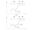
- FIG. 2 is a schematic diagram for explaining the attenuation characteristics of the filter in FIG. 1.
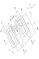
- FIG. FIG. 2 is a perspective view showing conductors of essential parts of the filter according to the first embodiment.
- FIG. 4 is a perspective view showing the first inductor extracted from FIG. 3;
- FIG. 4 is a perspective view showing a coupling line extracted from FIG. 3;
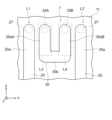
- FIG. 4 is a plan view of a portion of the configuration shown in FIG. 3;
- FIG. 7 is a diagram showing an equivalent circuit of a filter according to a second embodiment.
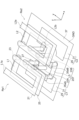
- FIG. 7 is a perspective view showing a conductor of a main part of a filter according to a second embodiment.
- FIG. 9 is a perspective view showing the first inductor extracted from FIG. 9;
- FIG. 10 is a perspective view showing a coupling line extracted from FIG. 9;
- FIG. 3 is a diagram illustrating an example of the use of a filter according to an embodiment.
- FIG. 1 is a circuit diagram showing an equivalent circuit of a filter 1 according to the first embodiment.
- the filter 1 filters, for example, the electrical signal flowing through the signal path 5 from the input terminal 3A to the output terminal 3B.
- the filter 1 includes, for example, one or more (in the illustrated example, a plurality of capacitors, more specifically, three) capacitors C11 to C13 that are included in the signal path 5 and are connected in series with each other. Further, the filter 1 includes two or more (two in the illustrated example) resonators Re1 and Re2 that connect the signal path 5 and the reference potential section GND.
- the resonator Re1 is configured as a series resonant circuit, for example. That is, the resonator Re1 includes an inductor L1 and a capacitor C1 that are connected in series with each other.
- the resonator Re2 is configured, for example, as a series resonant circuit and includes an inductor L2 and a capacitor C2 that are connected in series with each other.
- the resonant frequency of the resonator Re1 and the resonant frequency of the resonator Re2 are generally equivalent. Either the inductor or the capacitor may be on the signal path 5 side, but in the illustrated example, the inductor is on the signal path 5 side.
- the filter 1 has a coupling line 7 that magnetically couples the inductors L1 and L2.
- the coupling line 7 includes an inductor L3 that is magnetically coupled to the inductor L1, and an inductor L4 that is magnetically coupled to the inductor L2.
- the inductors L3 and L4 have one end connected to each other and the other end connected to the reference potential GND.
- the coupling line 7 is not connected to the signal path 5.
- FIG. 2 is a schematic diagram for explaining the attenuation characteristics of the filter 1.
- the upper diagram shows an example of the attenuation characteristic of a filter according to a comparative example.
- the lower diagram shows an example of the attenuation characteristic of the filter 1 according to the embodiment.
- the horizontal axis indicates the frequency f, and the frequency is higher on the right side of the figure.
- the vertical axis indicates the amount of attenuation, and the amount of attenuation is larger toward the bottom of the diagram.
- the filter according to the comparative example has a configuration in which the coupling line 7 is removed from the filter 1.
- the amount of attenuation in the pass band XB is small.
- the attenuation amount of the stop band EB adjacent to the low frequency side with respect to the pass band XB is large.
- the frequency band between the two is a transition band TB in which the amount of attenuation changes.
- Filter 1 and the filter according to the comparative example function as a high-pass filter that passes a signal having a frequency higher than the stop band EB (frequency of the pass band XB) from the input terminal 3A to the output terminal 3B.
- the capacitors C11 to C13 contribute to, for example, attenuating a signal having a frequency in the stop band EB while allowing a signal having a frequency in the pass band XB to pass.
- the resonators Re1 and Re2 contribute to forming the attenuation pole PL1 in the stopband EB.
- the frequency of this attenuation pole PL1 is the resonance frequency of each of the resonators Re1 and Re2. That is, the resonators Re1 and Re2 release a signal (unwanted component) having a resonant frequency located within the stop band EB to the reference potential portion GND.
- a new attenuation pole PL2 appears in the stop band EB compared to the attenuation characteristic of the filter according to the comparative example.
- the slope of the line indicating the attenuation characteristic can be made steep. Therefore, in the filter 1 according to the embodiment, compared to the filter according to the comparative example, for example, the attenuation amount in the stop band EB can be increased while the attenuation amount in the pass band XB is the same. That is, filter characteristics can be improved.
- the new attenuation pole PL2 appears because a new resonance mode is realized by magnetically coupling the two resonators Re1 and Re2 via the coupling line 7.
- FIG. 3 is a perspective view showing the conductors of the main parts of the filter 1.
- FIG. 4 is a perspective view showing the inductor L1 extracted from FIG. 3.
- FIG. 5 is a perspective view showing the coupling line 7 extracted from FIG. 3.
- FIG. 6 is a cross-sectional view of the filter 1 taken along line VI-VI in FIG.
- FIG. 7 is a plan view of a portion of the configuration shown in FIG. 3.
- the filter 1 may be used in any orientation with respect to the vertical direction, but for convenience, terms such as upper surface may be used with the +z side as upward. Furthermore, when referring to planar view or planar perspective, unless otherwise specified, it refers to viewing in the z direction.
- the z direction is defined parallel to the thickness direction of the circuit board 9, which will be described later.
- the x direction is defined to be parallel to the front and back surfaces of the circuit board 9, and parallel to the direction in which the inductors L1 and L2 are arranged.
- the y direction is a direction perpendicular to the x direction and the z direction.
- the filter 1 is composed of a circuit board 9.
- the circuit board 9 is configured by, for example, a multilayer board.
- a multilayer board includes, for example, a plurality of insulating layers 11 (11A to 11O) stacked on each other and conductor patterns (17, 21, 25, 29, 31, etc.; sometimes simply called patterns) that overlap each insulating layer 11. and a via conductor 15 penetrating each insulating layer 11. Note that in the description of the embodiments, two or more insulating layers 11 may be considered as one insulating layer.
- a conductor that includes one or more via conductors 15 and penetrates one or more insulating layers 11 may be referred to as a through conductor (27, 33A, 33B, etc.).
- the through conductor may include, for example, two or more via conductors 15, and may include one or more lands 17 (in other words, a conductor pattern) in addition to the one or more via conductors 15.
- Land 17 includes a flange-shaped portion connected to the upper end or lower end of via conductor 15. Note that, for example, when the via conductor 15 or the through conductor is expressed as extending upward or downward, the length in the z direction does not necessarily have to be larger than the diameter of the via conductor 15.
- FIG. 3 among the conductors of the filter 1, the conductors of the resonators Re1 and Re2 and the coupling line 7 are shown. That is, illustration of the input terminal 3A, output terminal 3B, and signal path 5 (capacitors C11 to C13) is omitted. These may be configured by conductor patterns and/or via conductors 15 as appropriate in areas of the circuit board 9 outside the range shown in FIG.
- the resonators Re1 and Re2 are, for example, configured to be substantially symmetrical to each other with respect to a plane of symmetry (not shown) parallel to the yz plane. Therefore, in the following description, matters that may be common to the resonators Re1 and Re2 will be described only for the resonator Re1. That is, the description regarding the resonator Re1 may be appropriately applied to the resonator Re2. Also, when describing only one resonator representing resonators Re1 and Re2 in this way, the code of the other resonator may be placed in parentheses immediately after the code of the one resonator. .
- the end L1a (L2a) of the inductor L1 (L2) is located on the +y side and +z side of the resonator Re1 (Re2).
- This end portion L1a (L2a) is a portion connected to the signal path 5.
- the inductor L1 (L2) as a whole generally extends from the end L1a (L2a) to the end L1b (L2b (FIG. 3) located below the end L1a (L2a). ) in a spiral shape.
- the end portion L1b (L2b) is connected to the capacitor C1 (C2) from above.
- the capacitor C1 (C2) is a parallel plate type having electrodes 29 and 31 facing each other in the z direction.
- the electrode 31 is constituted by a part of the reference potential section GND (GND pattern 37).
- the coupling line 7 has a gate-like shape as a whole. As shown in FIG. 3, the coupling line 7 is located between the two resonators Re1 and Re2. The two lower ends of the coupling line 7 are connected to the reference potential section GND (GND pattern 37). As indicated by the reference numerals in FIG. 7, the portion of the coupling line 7 that is magnetically coupled to the inductor L1 (L2) (the coupling through conductor 33A (33B) and the linear portion 35aA (35aB), which will be described later) is connected to the inductor L3 ( L4).
- the circuit board 9 shown in FIG. 6 has a plurality of insulating layers 11 stacked on each other.
- FIG. 6 may be interpreted as showing all the insulating layers 11 included in the circuit board 9, or may be taken as showing only a part of the insulating layers 11. That is, with respect to all of the illustrated insulating layers 11A to 11O, the insulating layer 11 overlapping the upper surface or the lower surface may or may not exist. However, in the following description, for convenience, it may be expressed as if such an insulating layer 11 does not exist.
- the basic structure and materials of the circuit board 9 may be the same as those of various known printed circuit boards.
- the circuit board 9 may be an LTCC (Low Temperature Co-fired Ceramics) substrate, an HTCC (High Temperature Co-Fired Ceramic) substrate, an IPD (Integrated Passive Device) substrate, or an organic substrate.
- Examples of LTCC substrates include those made by adding a glass-based material to alumina and allowing firing at low temperatures (for example, around 900° C.).
- LTCC substrate for example, Cu or Ag may be used as the conductive material.
- the IPD substrate include a Si substrate on which passive elements are formed.
- the organic substrate include a base material made of glass or the like laminated with prepreg impregnated with resin.
- the circuit board 9 may include an electronic element other than the filter 1, or the electronic element may be mounted on the front surface and/or the back surface.
- electronic elements include filters (other than filter 1), resistors, inductors, capacitors, and ICs (Integrated Circuits). These electronic elements may be electrically connected to the filter 1 to constitute a filter (including the filter 1), a duplexer, and/or a communication module.
- the insulating layer 11 is, for example, in the form of a layer that spreads with a constant thickness.
- the plurality of insulating layers 11 may have the same material and/or thickness, or may have different materials and/or thicknesses. In the example shown in FIG. 6, a plurality of insulating layers 11 having the same thickness are stacked, except for the insulating layer 11A. Note that each insulating layer 11 may be composed of two or more insulating layers.
- Each conductor pattern (17, 21, 25, 29, or 31, etc.) is, for example, in the form of a layer that spreads with a constant thickness. Furthermore, the plurality of conductor patterns located on the same layer are, for example, made of the same material and have the same thickness. Furthermore, the materials and/or thicknesses of the conductor patterns located in different layers may be the same (as shown in the figure) or may be different from each other.
- the via conductor 15 has a cylindrical and straight column shape with the z direction as the axis direction. Further, the plurality of via conductors 15 connected in series have the same shape and size, and the plurality of via conductors 15 as a whole have a columnar shape and a straight columnar shape.
- each via conductor 15 may have a tapered shape (truncated pyramid shape) in which the diameter decreases upwardly or downwardly.
- the via conductor 15 may have a hollow shape.
- the inside of the via conductor may be in a vacuum state, filled with gas, or filled with an insulating material.
- the diameters of the connected portions of the via conductors 15 connected to each other in series may be different from each other.
- the specific shape and dimensions of the land 17 may be set as appropriate.
- the land 17 has a circular shape whose center is common to the outer peripheral surface of the via conductor 15 when viewed from above. The difference in diameter between the two is arbitrary.
- the shapes and dimensions of the two or more lands 17 may be the same (as shown in the figure). For example, they may be different from each other.
- the land 17 may overlap the upper surface or the lower surface of the via conductor 15 (as shown in the figure), or the land 17 may have an annular shape (flange shape) as a whole, It may be connected to the side surface of the via conductor 15, or such a distinction may not be possible. Note that in the description of the embodiments, for convenience, expressions may be given based on the illustrated aspects. The land 17 may not be provided.
- the inductor L1 (L2) has a spiral shape as a whole.
- the axis of the helix is along (for example, parallel to) the z-direction.
- the number of turns of the spiral is arbitrary, and in the illustrated example, it is 1.5 or more and less than 2.
- the shape of the spiral viewed in the axial direction is arbitrary, and in the illustrated example, it is rectangular.
- the inductor L1 (L2) has a portion that extends linearly when viewed in the axial direction. More specifically, the rectangular shape is rectangular, and its longitudinal direction is the same direction (y direction) orthogonal to the direction in which the inductors L1 and L2 are arranged (x direction). In other words, the long sides of the inductors L1 and L2 face each other.
- the diameter of the helical shape may be constant in the axial direction (as in the illustrated example), or may not be constant.
- the inductor L1 (L2) when the inductor L1 (L2) is viewed in the axial direction include, for example, a circular shape, an elliptical shape, a polygonal shape other than a rectangle, and one or more sides of a polygon (for example, a pair of short sides of a rectangle).
- An example of this is a shape in which the sides (sides) are curved outward. The corners of polygons (including rectangles) may be chamfered.
- the inductor L1 (L2) does not have to extend in a spiral shape.
- the inductor L1 (L2) may extend in a C-shape, a spiral shape, or a meandering shape within one layer.
- the inductor L1 (L2) may be configured in a spiral shape with the axial direction parallel to the xy plane.
- the spiral shape of the inductor L1 (L2) in the illustrated example is realized by combining a conductor pattern and a through conductor. More specifically, the inductor L1 (L2) has a pattern 21, a through conductor 23, a pattern 25, and a through conductor 27 in this order from the end L1a (L2a) to the end L1b (L2b).
- the patterns 21 and 25 are located in different layers. Each pattern extends, for example, around a predetermined center point (not shown). Its specific shape is arbitrary. In the illustrated example, each pattern extends so as to form part of the four sides of a rectangle, as can be understood from the above description of the spiral shape. This rectangle has the same dimensions in both patterns. Further, for example, the patterns 21 and 25 overlap each other over most of the area (for example, 80% or more of the area of each pattern) in planar perspective. The angular range around the center point of each pattern is also arbitrary, for example, 270° or more and less than 360°. Each pattern extends, for example, with a constant width.
- the through conductor 23 connects the pattern 21 and the pattern 25 located in different layers so as to form a spiral shape. More specifically, the through conductor 23 is interposed between an end of the pattern 21 opposite to the end L1a (L2a) and one end of the pattern 25, and connects the two.
- the through conductor 27 is a portion extending downward (toward the -z side) from the spiral shape. More specifically, the through conductor 27 extends downward from the end of the pattern 25 that is opposite to the end connected to the through conductor 23 .
- the lower end of the through conductor 27 serves as an end portion L1b (L2b) of the inductor L1 (L2).
- the through conductors 23 and 27 may be located at arbitrary positions with respect to the shape formed by the patterns 21 and 25 (rectangular in the illustrated example). In another aspect, the positions of the ends of each pattern are arbitrary.
- the through conductors 23 and 27 of the inductor L1 (L2) are located in the portion (long side) of the patterns 21 and 25 on the inductor L2 (L1) side. More specifically, the through conductor 23 is located at an end (another From a viewpoint, it is located at the corner of a rectangle).
- the through conductor 27 is located on the +y side of the above-mentioned portion (long side) of the pattern 25 with respect to the center.
- the pattern 21 and the pattern 25 face each other with one or more insulating layers 11 (in the illustrated example, a plurality of insulating layers 11; more specifically, three insulating layers 11L to 11N) interposed therebetween.
- the penetrating conductor 23 includes one or more (three) via conductors 15 that respectively penetrate the one or more insulating layers 11 described above.
- the penetrating conductor 23 penetrates two or more (three in the illustrated example) insulating layers 11, one or more (two in the illustrated example) lands 17 located between the two or more insulating layers 17 have.
- the pattern 25 (in other words, the pattern of the lowest layer of the spiral portion) and the capacitor C1 (electrode 29) are composed of one or more insulating layers 11 (in the illustrated example, a plurality of layers; more specifically, 10 layers of insulating layers). 11B to 11K).
- the through conductor 27 has one or more (10) via conductors 15 that each penetrate one or more of the above-mentioned insulating layers 11 .
- the penetrating conductor 23 penetrates two or more layers (10 layers in the illustrated example) of the insulating layer 11, one or more (nine in the illustrated example) lands 17 located between the two or more insulating layers 17 have.
- the capacitor C1 (C2) is a parallel plate type having electrodes 29 and 31 facing each other in the z direction, and the electrode 31 is connected to the reference potential part GND (GND pattern 37). It is made up of. Unlike the illustrated example, the capacitor C1 (C2) may be formed by electrodes facing each other in the same layer, or may be formed by a pair of comb-teeth electrodes.
- reference potential section may refer to an individual conductor to which a reference potential is applied, or may refer to one or more conductors to which a reference potential is applied collectively as one reference potential section. In this disclosure, unless otherwise specified, the latter is assumed. Therefore, for example, when it is said that "the first inductor is connected to the reference potential section, and the second inductor is connected to the reference potential section", the first inductor and the second inductor are connected to the same conductor. It doesn't necessarily mean that Furthermore, the two or more conductors included in the reference potential section are not necessarily connected to each other within the filter 1 or within the circuit board 9.
- the GND pattern 37 is, for example, the lowest layer conductor pattern among a plurality of conductor patterns in the resonators Re1 and Re2, in the filter 1, and/or in the circuit board 9. It is made up of. Further, the GND pattern 37 is formed of a so-called solid pattern that spreads out without gaps. As already mentioned, the insulating layer 11 may be provided overlapping the GND pattern 37 from below (-z side).
- the planar shape and dimensions of the GND pattern 37 are arbitrary.
- the GND pattern 37 has a shape and area that overlaps at least the two capacitors C1 and C2 and the area between them in plan view.
- the GND pattern 37 includes at least the two resonators Re1 and Re2 (however, the portions of the inductors L1 and L2 that extend from the spiral shape toward the ends L1a and L2a) in plan view. (excluding) has an overlapping shape and area throughout.
- the electrode 29 faces the GND pattern 37 from above.
- a region of the GND pattern 37 that faces the electrode 29 functions as the electrode 31.
- the shape and dimensions of the electrode 29 are arbitrary.
- the electrode 29 has a rectangular shape. More specifically, the rectangular shape is rectangular, and its longitudinal direction is the same direction (y direction) orthogonal to the direction in which the capacitors C1 and C2 are arranged (x direction). From another perspective, the longitudinal direction of the electrode 29 is the same as the longitudinal direction of the inductor L1 (L2).
- capacitor C1 (C2) is contained in the spiral shape of inductor L1 (L2). More specifically, the helical shapes of capacitor C1 (C2) and inductor L1 (L2) have the same length in the y direction, and the length of capacitor C1 (C2) in the x direction is the same as that of inductor L1 (L2). It is shorter than the length of the shape in the x direction (for example, 1/3 or more and 4/5 or less). Furthermore, the edge of the capacitor C1 (C2) on the side of the resonator Re2 (Re1) and the edge of the inductor L1 (L2) on the side of the spiral resonator Re2 (Re1) generally coincide.
- the electrode 29 and the electrode 31 face each other with one insulating layer 11 (insulating layer 11A) interposed therebetween.
- the electrodes 29 and 31 may face each other with two or more insulating layers 11 in between.
- the lower end of the through conductor 27 of the inductor L1 (L2) is connected to the electrode 29.
- the connection position between the through conductor 27 and the electrode 29 is arbitrary.
- the through conductor 27 of the inductor L1 (L2) is It is connected to a portion of the electrode 29 of the capacitor C1 (C2) adjacent to the edge (long side) on the side of the capacitor C2 (C1).
- the coupling line 7 includes coupling through conductors 33A and 33B penetrating the insulating layer 11 in parallel with each other, and a coupling pattern 35 connecting the upper ends of the coupling conductors 33A and 33B. ing.
- the bonding pattern 35 extends, for example, to form three sides of a rectangle.
- the coupling line 7 is located between the two inductors L1 and L2.
- the coupling through conductor 33A (33B) and the through conductor 27 of the inductor L1 (L2) are adjacent to each other and extend in parallel to each other, and are magnetically coupled.
- One side of the coupling pattern 35 and one side of the pattern 25 of the inductor L1 (L2) are adjacent to each other and extend in parallel to each other, and are magnetically coupled.
- a portion of the coupling line 7 that is magnetically coupled to the inductor L1 (L2) constitutes an inductor L3 (L4). That is, the inductor L3 (L4) has a coupling through conductor 33A (33B) and one side of the coupling pattern 35 (a linear portion 35aA (35aB) to be described later). Note that, unlike the illustrated example, the inductor L3 (L4) may be configured by only the coupling through conductor 33A (33B) or only a part of the coupling pattern 35.
- the position of the coupling through conductor 33A (33B) with respect to the through conductor 27 of the inductor L1 (L2) is arbitrary as long as both can be magnetically coupled.
- coupling through conductors 33A and 33B are located on a straight line connecting through conductors 27 of inductors L1 and L2. That is, the four through conductors 27 are arranged in one row.
- the distance between the coupling through conductor 33A (33B) and the through conductor 27 of the inductor L1 (L2) is, for example, shorter than the distance between the coupling through conductors 33A and 33B.
- the distance between the through conductors refers to the distance between the axes unless otherwise specified.
- the distance between the coupling through conductor 33A (33B) and the through conductor 27 of the inductor L1 (L2) is, for example, 0.05 mm or more and 0.4 mm or less.
- both of them are connected to one or more insulators. Both pass through layer 11. In the example shown in FIG. 6, both pass through ten insulating layers 11B to 11K. Note that, as described above, the insulating layers 11B to 11K may be regarded as one insulating layer.
- the relative length (z direction) of the coupling through conductor 33A (33B) to the through conductor 27 of the inductor L1 (L2) is arbitrary.
- the coupling through conductor 33A (33B) extends over the entire length of the through conductor 27. More specifically, the upper end of the coupling through conductor 33A (33B) is located in the same layer as the upper end of the through conductor 27 (the layer where the pattern 25 is located). Further, the lower end of the coupling through conductor 33A (33B) is located below the lower end of the through conductor 27. The difference in the positions of both lower ends corresponds to the thickness of the capacitor C1.
- the shape and dimensions (excluding the length in the z direction) of the coupling through conductor 33A (33B) may be the same as the shape and diameter of the through conductor 27 (example shown), or may be different. .
- the position of the upper end of the coupling through conductor 33A (33B) and the position of the upper end of the through conductor 27 may be different.
- the position in the z direction of the coupling pattern 35 that connects the upper ends of the coupling through conductors 33A and 33B is different from the position of the pattern 25 in the z direction. Therefore, when magnetically coupling the conductor pattern included in the coupling line 7 and the pattern 25, for example, instead of the coupling pattern 35, two patterns connected to the upper ends of the coupling through conductors 33A and 33B and the pattern A pattern magnetically coupled to the pattern 25 and two through conductors connecting the former two patterns and the latter pattern may be provided in the same layer as the pattern 25.
- the coupling through conductor 33A (33B) is a portion of the coupling line 7 that is directly connected to the reference potential portion GND (GND pattern 37). From another point of view, the coupling through conductor 33A is a portion connecting the coupling pattern 35 and the reference potential portion GND. Further, the through conductor 27 is a portion of the inductor L1 (L2) that is directly connected to the capacitor C1 (C2). From another perspective, the through conductor 27 is a portion connecting the pattern 25 and the capacitor C1 (C2). From yet another perspective, the through conductor 27 is a portion of the inductor L1 (L2) that is electrically located closest to the reference potential portion GND.
- the through conductor 27 is connected to one side of the spiral portion (pattern 25 from another perspective) of the inductor L1 (L2) on the side of the coupling line 7 in plan view. From another viewpoint, the through conductor 27 is located closest to the coupling line 7 (from another viewpoint, the inductor L3 (L4)) among the inductors L1 (L2). Further, the coupling through conductor 33A (33B) is located at the position closest to the inductor L1 (L2) among the coupling lines 7 (inductor L3 (L4) from another viewpoint) in plan view.
- the magnetic field coupling between the through conductor 27 and the coupling through conductor 33A (33B) is the magnetic field coupling between the inductors L1 (L2) and inductors L3 (L4) at their closest positions.
- the positions of the axes (centers) may be the closest, or the positions of the outer edges (edges of the lands 17) may be the closest.
- one side of the pattern 25 that is magnetically coupled to the coupling pattern 35 is referred to as a linear portion 25a.
- One side of the coupling pattern 35 that is magnetically coupled to the pattern 25 of the inductor L1 is referred to as a linear portion 35aA.
- one side of the coupling pattern 35 that is magnetically coupled to the pattern 25 of the inductor L2 is referred to as a linear portion 35aB.
- the portion connecting the linear portion 35aA and the linear portion 35aB will be referred to as a connecting portion 35b.
- the linear portion 25a extends in the direction (y direction) orthogonal to the direction in which the two inductors L1 and L2 are lined up (x direction).
- the linear portion 35aA (35aB) extending parallel to the linear portion 25a also extends in the y direction.
- the length (y direction) of the linear portion 35aA (35aB) may be shorter than the length of the linear portion 25a (as shown in the figure), equal to or longer than the length of the linear portion 25a. Setting the specific length of the linear portion 35aA (35aB) may be used, for example, to adjust the strength of the magnetic field coupling between the inductor L1 (L2) and the inductor L3 (L4). At this time, the linear portion 35aA (35aB) may not be provided.
- the linear portion 35aA (35aB) extends, for example, in the y direction from the position of the coupling through conductor 33A (33B). Further, the linear portion 25a extends in the y direction from the position of the through conductor 27. Therefore, the above explanation regarding the distance between the coupling through conductor 33A (33B) and the through conductor 27 of the inductor L1 (L2) is the distance between the straight part 35aA (35aB) and the straight part 25a of the inductor L1 (L2). may be used in the explanation of Here, the distance between linear portions refers to the distance between their center lines.
- the connecting portion 35b extends linearly with the same width as the linear portions 35aA and 35aB.
- the connecting portion 35b may be formed in a curved shape that swells outward, or may have a width different from the width of the linear portions 35aA and 35aB.
- the filter according to the comparative example in which the coupling line 7 is removed from the filter 1 has a known configuration. Therefore, the inductances of inductors L1 and L2 and the capacitances of capacitors C1, C2 and C11-C13 may be set by methods similar to known methods. However, fine adjustment may be made in consideration of the influence of the coupling line 7.
- the inductance of the inductors L3 and L4 and the strength of the magnetic field coupling of the inductors L1 and L3 (L2 and L4) may also be set appropriately. For example, as follows.
- the coupling line 7 can be regarded as creating mutual inductance between the inductors L1 and L2.
- the current generated by the magnetic field coupling of the inductors L1 and L3 and the current generated by the magnetic field coupling of the inductors L2 and L4 run in opposite directions of the coupling line 7. flows to That is, the above mutual inductance is negative.
- the inductance obtained by combining the inductance of the inductor L1 (L2) and the mutual inductance is smaller than the inductance of the inductor L1 (L2).
- a resonator having a higher resonant frequency than resonator Re1 (Re2) is substantially configured.
- a new attenuation pole PL2 appears at a frequency higher than the resonance frequency of the resonator Re1 (Re2) alone (the frequency of the attenuation pole PL1).
- the absolute value of the mutual inductance becomes larger, and the frequency of the attenuation pole PL2 shifts from the frequency of the attenuation pole PL1 to the higher frequency side.
- the filter 1 includes a filter element (capacitor C12), a first resonator (resonator Re1), a second resonator (resonator Re2), a third inductor (inductor L3), and a fourth inductor. (inductor L4).
- Capacitor C12 is included in the signal path 5 from the input side to the output side.
- the resonator Re1 connects a portion of the signal path 5 that is electrically input to the capacitor C12 and the reference potential section GND, and includes a first inductor (inductor L1).
- the resonator Re2 connects a portion of the signal path 5 that is electrically output to the capacitor C12 and the reference potential section GND, and includes a second inductor (inductor L2).
- Inductor L3 is magnetically coupled to inductor L1.
- Inductor L4 is magnetically coupled to inductor L2.
- the inductors L3 and L4 have one end side connected to the reference potential part GND separately from each other (instead of connecting the one ends to each other and then connecting to the reference potential part GND), and connect the inductors L3 and L4 to the reference potential part GND separately.
- the parts that are electrically opposite to the connected side are connected to each other and are not electrically connected to the signal path 5.
- a new attenuation pole PL2 can be formed and the slope of the line showing the attenuation characteristic in the transition band TB can be made steeper. That is, the characteristics of the filter 1 can be improved.
- the inductors L3 and L4 have one end side connected to the reference potential GND separately from each other, compared to, for example, a mode in which the inductors L3 and L4 are part of an annular pattern in an electrically floating state. , it is easy to adjust the strength of magnetic field coupling.
- an electromagnetic field distribution occurs in a steady state in which the sum of the squares of the electric field amplitude and the magnetic field amplitude is constant.
- the amplitude of the magnetic field is large in the portion where the amplitude of the electric field is small.
- the amplitude of the electric field in the reference potential portion GND is approximately 0.
- One ends of inductors L3 and L4 connected to reference potential section GND also have a small amplitude of the electric field, so one end side of inductors L3 and L4 connected to reference potential section GND have a large amplitude of magnetic field and Easy to combine.
- the inductors L3 and L4 are not electrically connected to the signal path 5, they do not directly affect the filter characteristics of the signal path 5 like the resonator Re1 (Re2). Therefore, the magnetic field coupling strength and/or inductance can be set for inductors L3 and L4 without considering such direct effects. As a result, design is facilitated.
- the resonator Re1 may include a first capacitor (capacitor C1) connecting the inductor L1 and the reference potential section GND.
- the resonator Re1 may be a series resonator, and the inductor L1 is relatively electrically separated from the reference potential section GND by interposing the capacitor C1 between it and the reference potential section GND. It's okay to stay.
- the Q value of the inductor L1 (L2) can be improved.
- the inductor L1 may include a first element (for example, the linear portion 25a) and a second element (for example, the through conductor 27) connecting the first element and the capacitor C1.
- the inductor L3 may include a third element (for example, the linear part 35aA) and a fourth element (for example, the coupling through conductor 33A) connecting the third element and the reference potential part GND.
- the second element and the fourth element may extend in parallel to each other and may be magnetically coupled.
- the portions of the inductor L1 and the inductor L3 that are relatively close to the reference potential portion GND may be magnetically coupled to each other.
- the amplitude of the magnetic field is small in the parts of the inductor L1 and the inductor L3 (second element and fourth element) near the reference potential part GND, so the amplitude of the magnetic field is small. is large and magnetic field coupling is easy. Therefore, it is easy to adjust the strength of the magnetic field coupling between the inductors L1 and L3. Furthermore, it is easy to strengthen the magnetic field coupling between, for example, the inductors L1 and L3.
- the filter 1 may have a circuit board 9 including a first insulating layer (a combination of insulating layers 11B to 11K).
- the second element may include a first through conductor (through conductor 27) that penetrates the first insulating layer in the thickness direction (z direction).
- the fourth element described above may include a second through conductor (coupling through conductor 33A) that penetrates the first insulating layer in the thickness direction.
- the through conductor 27 and the coupling through conductor 33A may extend in parallel to each other and may be magnetically coupled.
- the length of the magnetic field coupling between the inductors L1 and L3 is determined by the length of the circuit board 9. This is advantageous in reducing the size of the circuit board 9 in the planar direction.
- the inductors L1 and L3 are likely to have a structure including a through conductor extending to the lower surface.
- the through conductor 27 may be located closest to the inductor L3 in the inductor L1.
- the coupling through conductor 33A may be located closest to the inductor L1 in the inductor L3.
- the strength of the magnetic field coupling by the through conductor 27 and the coupling through conductor 33A can be increased.
- the probability that magnetic field coupling will occur between portions that are not intended for magnetic field coupling is reduced.
- the strength of the magnetic field coupling between the inductor L1 and the coupling line 7 can be easily adjusted by the distance and/or size of the through conductor 27 and the coupling through conductor 33A.
- the distance between the axis of the through conductor 27 and the axis of the coupling through conductor 33A may be 0.05 mm or more and 0.4 mm or less.
- the first element described above may have a first pattern (pattern 25) overlapping the first insulating layer (combination of insulating layers 11B to 11K).
- the third element described above may have a second pattern (coupling pattern 35) overlapping the first insulating layer.
- the pattern 25 and the coupling pattern 35 may have linear portions 25a and 35aA extending in parallel to each other.
- magnetic field coupling is performed not only between through-hole conductors, but also between conductor patterns, making it easier to strengthen the strength of magnetic field coupling.
- not only the magnetic field coupling by the second element and the fourth element near the reference potential part GND but also the magnetic field coupling by the first element and the third element far from the reference potential part GND are performed. This makes it easier to increase the strength of the material.
- FIG. 8 is a circuit diagram showing an equivalent circuit of the filter 201 according to the second embodiment. This figure corresponds to FIG. 1 of the first embodiment.
- the filter 201 (coupling line 207) is electrically opposite to the side of the inductors L3 and L4 that is connected to the reference potential section GND. It has an inductor L5 that connects the parts. Thereby, for example, the strength of magnetic field coupling can be substantially increased.
- FIG. 9 is a perspective view showing the main conductors of the filter 201 according to the second embodiment, and corresponds to FIG. 3 of the first embodiment.
- FIG. 10 is a perspective view showing the inductor L1 extracted from FIG. 9, and corresponds to FIG. 4 of the first embodiment.
- FIG. 11 is a perspective view showing the coupling line 207 extracted from FIG. 9, and corresponds to FIG. 5 of the first embodiment.
- the configuration of the inductor L1 (L2) in this embodiment is roughly the same as the configuration of the inductor L1 (L2) in the first embodiment.
- the through conductor 27 is not directly connected to the electrode 29 of the capacitor C1 (C2).
- the lower end of the through conductor 41 is an end portion L1b (L2b (FIG. 9)) of the inductor L1 (L2).
- the capacitor C1 (C2) of this embodiment is located on the opposite side of the coupling line 207 with respect to the inductor L1 (L2), contrary to the first embodiment. are doing. More specifically, in plan view, the opposite edge of the capacitor C1 (C2) and the opposite edge of the inductor L1 (L2) generally match. Further, the electrode 29 of the capacitor C1 (C2) has a recessed portion (number omitted) at the edge on the coupling line 207 side.
- the straight portions 35aA and 35bB are not connected by the connecting portion 35b (FIG. 5) in the same layer as these, but by the inductor L5. ing.
- the inductor L5 has a through conductor 43A (43B) extending downward from the linear portion 35aA (35aB) and a pattern 45 connecting the lower ends of the through conductors 43A and 43B, as indicated by the reference numerals in FIG. are doing. Thereby, the length of the coupling line 207 is ensured, and the inductor L5 is configured.
- the connecting portion 35b of the first embodiment can also function as an inductor.
- the connecting portion 35b connects the ends of the inductors L3 and L4 with the shortest distance. From another point of view, the connecting portion 35b is linear. Therefore, if the part connecting inductors L3 and L4 does not connect them at the shortest distance (not in a straight line), it may be considered that inductor L5 is provided.
- the configuration of such inductor L5 is not limited to that shown.
- the inductor L5 may be configured only with a conductor pattern that bends as appropriate, or may include four or more through conductors and move up and down two or more times.
- the inductor L5 may include four or more through conductors
- the inductor L5 in the illustrated example has two through conductors 43A connected to the two straight portions 35aA and 35aB. and 43B, and a conductor (one or more conductor patterns and zero or more through conductors) that connects the two or more through conductors on opposite sides of the two linear parts 35aA and 35aB. can.
- the coupling through conductor 33A (33B) is adjacent to the through conductor 27 of the inductor L1 (L2) on the inductor L2 (L1) side. They are adjacent to each other in the direction (y direction) orthogonal to the direction in which the inductors L1 and L2 are lined up.
- the linear portion 35aA (35aB) is not adjacent to the linear portion 25a of the inductor L1 (L2) on the inductor L2 (L1) side, but is adjacent to the lower side. are doing.
- Such a configuration makes it easy to increase the inductance of the inductor L5 by elongating the inductor L5 (more specifically, the pattern 45), for example.
- Such a configuration also facilitates, for example, reducing the dimension of the filter in the x direction.
- Filters 1 and 201 may be used, for example, in a communication module and/or a communication device. An example is shown below. In addition, below, for convenience, only the code
- FIG. 12 is a block diagram showing the main parts of a communication device 151 as an example of how the filter 1 is used.
- the communication device 151 includes a module 171 and a housing 173 that accommodates the module 171.
- the module 171 performs wireless communication using radio waves, and includes a duplexer 101.
- the branching filter 101 is a duplexer having a transmission filter 103 and a reception filter 105.
- the filter 1 is applied to a portion of at least one of the transmission filter 103 and the reception filter 105.
- the transmission information signal TIS containing the information to be transmitted is modulated and frequency increased (converted to a high frequency signal having a carrier frequency) by an RF-IC (Radio Frequency Integrated Circuit) 153 (an example of an integrated circuit element). is made into a transmission signal TS.
- the transmission signal TS has unnecessary components outside the transmission passband removed by a bandpass filter 155, is amplified by an amplifier 157, and is input to the duplexer 101.
- the duplexer 101 (transmission filter 103) removes unnecessary components outside the transmission passband from the input transmission signal TS, and outputs the removed transmission signal TS to the antenna 159.
- the antenna 159 converts the input electrical signal (transmission signal TS) into a wireless signal (radio wave) and transmits the signal.
- the wireless signal (radio wave) received by the antenna 159 is converted into an electric signal (received signal RS) by the antenna 159 and input to the duplexer 101 .
- the duplexer 101 (reception filter 105) removes unnecessary components outside the reception passband from the input reception signal RS, and outputs the result to the amplifier 161.
- the output reception signal RS is amplified by an amplifier 161, and a bandpass filter 163 removes unnecessary components outside the reception passband.
- the received signal RS is then lowered in frequency and demodulated by the RF-IC 153 to become a received information signal RIS.
- the transmission information signal TIS and the reception information signal RIS may be low frequency signals (baseband signals) containing appropriate information, such as analog audio signals or digitized audio signals.
- the passband of the wireless signal may be set as appropriate.
- the modulation method may be phase modulation, amplitude modulation, frequency modulation, or a combination of two or more of these.
- a direct conversion system is shown as the circuit system, any other appropriate circuit system may be used, for example, a double superheterodyne system may be used.
- FIG. 12 schematically shows only the main parts, and a low-pass filter, an isolator, etc. may be added at an appropriate position, or the position of an amplifier, etc. may be changed.
- the module 171 has, for example, components from the RF-IC 153 to the antenna 159 on the same circuit board. That is, the transmission filter 103 and the reception filter 105 are modularized by being combined with other components.
- This circuit board may be the circuit board 9, or may be one on which the circuit board 9 is mounted. Note that the transmission filter 103 and the reception filter 105 may be included in the communication device 151 without being modularized.
- the components illustrated as the components of the module 171 may be located outside the module or may not be housed in the housing 173. For example, the antenna 159 may be exposed outside the housing 173.
- the transmission filter 103 includes the filter 1
- the input terminal 3A is connected to the amplifier 157
- the output terminal 3B is connected to the antenna 159
- the reception filter 105 includes the filter 1
- the input terminal 3A is connected to the antenna 159
- the output terminal 3B is connected to the amplifier 161, for example.
- another filter may be provided between the input terminal 3A and the filter 1 and/or between the filter 1 and the output terminal 3B.
- the other filter may be, for example, an elastic wave filter that uses elastic waves.
- the capacitor C12 is an example of a filter element included in the signal path.
- Resonators Re1 and Re2 are examples of a first resonator and a second resonator, respectively.
- Inductors L1, L2, L3, L4, and L5 are examples of a first inductor, a second inductor, a third inductor, a fourth inductor, and a fifth inductor, respectively.
- Capacitor C1 is an example of a first capacitor.
- the linear portion 25a and the through conductor 27 are examples of the first element and the second element, respectively.
- the linear portion 35aA and the coupling through conductor 33A are examples of the third element and the fourth element, respectively.
- the entire insulating layers 11B to 11K are an example of a first insulating layer.
- the through conductor 27 and the coupling through conductor 33A are examples of a first through conductor and a second through conductor, respectively.
- the linear portion 25a and the linear portion 35aA are examples of a first pattern and a second pattern, respectively.
- the first embodiment and the second embodiment may be combined as appropriate.
- the inductor L5 of the second embodiment is applied to a mode in which the coupling through conductor 33A (33B) and the through conductor 27 of the inductor L1 (L2) are adjacent to each other in the x direction, as in the first embodiment. It's okay.
- the coupling through conductor 33A (33B) and the through conductor 27 of the inductor L1 (L2) are adjacent to each other in the y direction, as in the second embodiment. It may be applied to the embodiment.
- a new attenuation pole PL2 is formed on the higher frequency side with respect to the attenuation pole PL1 of the single resonator Re1 (Re2). Differently from this, the new attenuation pole PL2 may be formed on the lower frequency side with respect to the attenuation pole PL1.
- the inductors L3 and L4 may be connected to each other such that the currents generated by the inductors L3 and L4 flow in the same direction through the coupling line (so that the mutual inductance is positive).
- the first resonator and the second resonator are series resonators.
- these resonators may be parallel resonators in which an inductor and a capacitor are connected in parallel.
- the third inductor and the fourth inductor contribute to forming a new pole on the lower frequency side or higher frequency side with respect to the pole of the first resonator (second resonator) alone.
- the filter element (capacitor C12) included in the signal path is not limited to a capacitor.
- the filter element has a function of, for example, allowing the passage of a signal having a frequency in the passband, and making the connection positions of the first resonator and the second resonator to the signal path electrically different from each other. It may be made into various electronic devices.
- the filter element may be a resonator, a resistor, or an inductor, or may be configured by combining two or more electronic elements.
- the filter may include two or more filter elements included in the signal path and three or more resonators (including a first resonator and a second resonator) connecting the signal path and the reference potential section.
- the first resonator and the second resonator may be two resonators among three or more resonators whose connection positions to the signal path are electrically adjacent to each other (in the embodiment (example shown in the explanation), this does not have to be the case.
- the resonator may serve as a second resonator and may be magnetically coupled to the resonator Re1 as the first resonator.
Landscapes
- Engineering & Computer Science (AREA)
- Power Engineering (AREA)
- Physics & Mathematics (AREA)
- Electromagnetism (AREA)
- Coils Or Transformers For Communication (AREA)
Abstract
フィルタにおいて、フィルタ素子は、入力側から出力側への信号経路に含まれている。第1共振器は、信号経路のうちフィルタ素子に対して電気的に入力側となる部位と、基準電位部とを接続しており、第1インダクタを有している。第2共振器は、信号経路のうちフィルタ素子に対して電気的に出力側となる部位と、基準電位部とを接続しており、第2インダクタを有している。第3インダクタは、第1インダクタと磁界結合する。第4インダクタは、第2インダクタと磁界結合する。第3インダクタ及び第4インダクタは、それぞれの一端側が互いに別々に基準電位部に接続されており、基準電位部に接続される側とは電気的に反対側の部分同士が互いに接続されており、信号経路に電気的に非接続とされている。
Description
本開示は、電気信号をフィルタリングするフィルタ及び当該フィルタを含む通信装置に関する。
フィルタとして、磁界結合を利用するものが知られている(例えば特許文献1)。特許文献1のフィルタは、2つの共振器を有している。2つの共振器は、信号経路と基準電位部とを互いに別個に接続している。各共振器は、インダクタとキャパシタとが並列接続された並列共振器とされている。2つの並列共振器は、インダクタ同士が磁界結合する。磁界結合は、インダクタ同士で直接的に行われるとともに、環状導体を介して行われる。
本開示の一態様に係るフィルタは、フィルタ素子と、第1共振器と、第2共振器と、第3インダクタと、第4インダクタと、を有している。前記フィルタ素子は、入力側から出力側への信号経路に含まれている。前記第1共振器は、前記信号経路のうち前記フィルタ素子に対して電気的に前記入力側となる部位と、基準電位部とを接続しており、第1インダクタを有している。前記第2共振器は、前記信号経路のうち前記フィルタ素子に対して電気的に前記出力側となる部位と、前記基準電位部とを接続しており、第2インダクタを有している。前記第3インダクタは、前記第1インダクタと磁界結合する。前記第4インダクタは、前記第2インダクタと磁界結合する。前記第3インダクタ及び前記第4インダクタは、それぞれの一端側が互いに別々に前記基準電位部に接続されており、前記基準電位部に接続される側とは電気的に反対側の部分同士が互いに接続されており、前記信号経路に電気的に非接続とされている。
本開示の一態様に係る通信装置は、上記フィルタと、当該フィルタに接続されている集積回路素子と、を有している。
以下、本開示に係る実施形態について、図面を参照して説明する。なお、以下の説明で用いられる図は模式的なものである。従って、例えば、図面上の寸法比率等は現実のものとは必ずしも一致していない。また、寸法比率等が図面同士で一致しないこともある。特定の形状及び/又は寸法等が誇張されたり、細部が省略されたりすることがある。ただし、上記は、実際の形状及び/又は寸法が図面の通りとされたり、図面から形状及び/又は寸法の特徴が抽出されたりしてもよいことを否定するものではない。
<第1実施形態>
以下では、概略、下記の順に第1実施形態に係る説明を行う。すなわち、まず、第1実施形態に係るフィルタの概要について述べ、次に、当該フィルタを実現する具体的な構造の一例について説明し、その後、第1実施形態についてまとめを述べる。
1.フィルタの概要
2.フィルタの構造の一例
3.第1実施形態のまとめ
以下では、概略、下記の順に第1実施形態に係る説明を行う。すなわち、まず、第1実施形態に係るフィルタの概要について述べ、次に、当該フィルタを実現する具体的な構造の一例について説明し、その後、第1実施形態についてまとめを述べる。
1.フィルタの概要
2.フィルタの構造の一例
3.第1実施形態のまとめ
(1.フィルタの概要)
図1は、第1実施形態に係るフィルタ1の等価回路を示す回路図である。
図1は、第1実施形態に係るフィルタ1の等価回路を示す回路図である。
フィルタ1は、例えば、入力端子3Aから出力端子3Bまでの信号経路5を流れる電気信号をフィルタリングする。フィルタ1は、例えば、信号経路5に含まれ、互いに直列に接続されている1以上(図示の例では複数。より詳細には3つ。)のキャパシタC11~C13を有している。また、フィルタ1は、信号経路5と基準電位部GNDとを接続する2以上(図示の例では2つ)の共振器Re1及びRe2を有している。
共振器Re1は、例えば、直列共振回路として構成されている。すなわち、共振器Re1は、互いに直列に接続されているインダクタL1及びキャパシタC1を有している。同様に、共振器Re2は、例えば、直列共振回路として構成されており、互いに直列に接続されているインダクタL2及びキャパシタC2を有している。共振器Re1の共振周波数と共振器Re2の共振周波数とは概ね同等とされている。インダクタ及びキャパシタは、いずれが信号経路5側であってもよいが、図示の例では、インダクタが信号経路5側となっている。
さらに、フィルタ1は、インダクタL1とL2とを磁界結合する結合用ライン7を有している。結合用ライン7は、インダクタL1と磁界結合するインダクタL3と、インダクタL2と磁界結合するインダクタL4とを有している。インダクタL3及びL4は、一端側が互いに接続されているとともに、他端側が基準電位部GNDに接続されている。結合用ライン7は、信号経路5に接続されていない。
図2は、フィルタ1の減衰特性を説明するための模式図である。
図2において、上段の図は比較例に係るフィルタの減衰特性の例を示している。下段の図は実施形態に係るフィルタ1の減衰特性の例を示している。上段の図及び下段の図それぞれにおいて、横軸は周波数fを示し、図の右側ほど周波数が高い。また、縦軸は、減衰量を示し、図の下側ほど減衰量が大きい。
比較例に係るフィルタは、フィルタ1から結合用ライン7を無くした構成を有している。フィルタ1及び比較例に係るフィルタの減衰特性においては、通過帯域XBの減衰量が小さくなっている。また、通過帯域XBに対して低周波数側に隣接する阻止帯域EBの減衰量が大きくなっている。両者の間の周波数帯は、減衰量が変化する遷移帯域TBとなっている。フィルタ1及び比較例に係るフィルタは、阻止帯域EBよりも周波数が高い周波数(通過帯域XBの周波数)を有する信号を入力端子3Aから出力端子3Bへ通過させるハイパスフィルタとして機能する。
比較例に係るフィルタにおいて、キャパシタC11~C13は、例えば、阻止帯域EBの周波数を有する信号を減衰させつつ、通過帯域XBの周波数を有する信号の通過を許容することに寄与している。共振器Re1及びRe2は、阻止帯域EBに減衰極PL1を形成することに寄与している。この減衰極PL1の周波数は、共振器Re1及びRe2それぞれの共振周波数である。すなわち、共振器Re1及びRe2は、阻止帯域EB内に位置する共振周波数を有する信号(不要成分)を基準電位部GNDに逃がす。
実施形態に係るフィルタ1の減衰特性では、比較例に係るフィルタの減衰特性に対して、阻止帯域EBに新たな減衰極PL2が現れている。これにより、例えば、遷移帯域TBにおいて、減衰特性を示す線の傾きを急峻にできる。よって、実施形態に係るフィルタ1においては、比較例に係るフィルタに比べて、例えば、通過帯域XBの減衰量を同等にしながら、阻止帯域EBの減衰量を大きくすることができる。すなわち、フィルタ特性を向上させることができる。新たな減衰極PL2が現れるのは、2つの共振器Re1及びRe2が結合用ライン7を介して磁界結合することによって、新たな共振モードが実現されることによる。
(2.フィルタの構造の一例)
上記のようなフィルタ1を実現する具体的な構造は種々可能である。以下に、その一例について説明する。以下の説明では、概略、下記の順に説明を行う。
2.1.構造の一例の概要
2.2.多層基板
2.3.インダクタL1及びL2
2.4.キャパシタC1及びC2(基準電位部GND)
2.5.結合用ライン
上記のようなフィルタ1を実現する具体的な構造は種々可能である。以下に、その一例について説明する。以下の説明では、概略、下記の順に説明を行う。
2.1.構造の一例の概要
2.2.多層基板
2.3.インダクタL1及びL2
2.4.キャパシタC1及びC2(基準電位部GND)
2.5.結合用ライン
(2.1.構造の一例の概要)
図3は、フィルタ1の要部の導体を示す斜視図である。図4は、図3からインダクタL1を抽出して示す斜視図である。図5は、図3から結合用ライン7を抽出して示す斜視図である。図6は、図3のVI-VI線におけるフィルタ1の断面図である。図7は、図3に示す構成の一部の平面図である。
図3は、フィルタ1の要部の導体を示す斜視図である。図4は、図3からインダクタL1を抽出して示す斜視図である。図5は、図3から結合用ライン7を抽出して示す斜視図である。図6は、図3のVI-VI線におけるフィルタ1の断面図である。図7は、図3に示す構成の一部の平面図である。
これらの図には、直交座標系xyzを付している。フィルタ1は、鉛直方向に対して任意の向きで利用されてよいが、便宜上、+z側を上方として、上面等の用語を用いることがある。また、平面視又は平面透視というとき、特に断りが無い限り、z方向に見ることを指すものとする。なお、z方向は、後述する回路基板9の厚み方向に平行に定義されている。x方向は、回路基板9の表面及び裏面に平行で、インダクタL1及びL2の並び方向に平行に定義されている。y方向は、x方向及びz方向に直交する方向である。
図6から理解されるように、フィルタ1は、回路基板9によって構成されている。回路基板9は、例えば、多層基板によって構成されている。多層基板は、例えば、互いに積層された複数の絶縁層11(11A~11O)と、各絶縁層11に重なる導体パターン(17、21、25、29及び31等。単にパターンということもある。)と、各絶縁層11を貫通するビア導体15とを有している。なお、実施形態の説明では、2以上の絶縁層11を1つの絶縁層として捉えることがある。
実施形態の説明では、1以上のビア導体15を含み、1以上の絶縁層11を貫通する導体を貫通導体(27、33A及び33B等)と称することがある。貫通導体は、例えば、2以上のビア導体15を含んでよく、また、1以上のビア導体15に加えて、1以上のランド17(換言すれば導体パターン)を含んでよい。ランド17は、ビア導体15の上端又は下端に接続されているフランジ状部分を含んでいる。なお、例えば、ビア導体15又は貫通導体について、上方又は下方に延びると表現するとき、必ずしもz方向の長さがビア導体15の径よりも大きいことは要しない。
図3では、フィルタ1の導体のうち、共振器Re1及びRe2並びに結合用ライン7の導体が示されている。すなわち、入力端子3A、出力端子3B及び信号経路5(キャパシタC11~C13)の図示は省略されている。これらは、回路基板9のうちの図3に示された範囲外の領域において、導体パターン及び/又はビア導体15によって適宜に構成されてよい。
共振器Re1及びRe2は、例えば、yz平面に平行な不図示の対称面に対して概ね互いに面対称に構成されている。従って、以下の説明では、共振器Re1及びRe2に共通してよい事項については、共振器Re1についてのみ説明することがある。すなわち、共振器Re1についての説明は、適宜に共振器Re2に援用されてよい。また、このように共振器Re1及びRe2を代表して一方の共振器のみについて説明するとき、当該一方の共振器の符号の直後に、他方の共振器の符号を括弧で括って付すことがある。共振器Re1及びRe2が含む構成要素(インダクタL1及びL2並びにキャパシタC1及びC2)についても同様とし、また、共振器Re1及びRe2に対応して設けられた部位(例えば後述する結合用貫通導体33A及び33B)についても同様とする。
図3において、共振器Re1(Re2)の+y側かつ+z側には、インダクタL1(L2)の端部L1a(L2a)が位置している。この端部L1a(L2a)は、信号経路5に接続される部分である。図4に示されているように、インダクタL1(L2)は、全体として、概略、端部L1a(L2a)から端部L1a(L2a)よりも下方に位置する端部L1b(L2b(図3))へ螺旋状に延びる形状とされている。図3に示されているように、端部L1b(L2b)は、キャパシタC1(C2)に上方から接続されている。キャパシタC1(C2)は、z方向において互いに対向する電極29及び31を有する平行平板型のものとされている。電極31は、基準電位部GND(GNDパターン37)の一部によって構成されている。
図5に示されているように、結合用ライン7は、全体として門型の形状とされている。図3に示されているように、結合用ライン7は、2つの共振器Re1及びRe2の間に位置している。結合用ライン7の2つの下端は、基準電位部GND(GNDパターン37)に接続されている。図7に符号を付すように、結合用ライン7のうち、インダクタL1(L2)に磁界結合する部分(後述する結合用貫通導体33A(33B)及び直線状部35aA(35aB))がインダクタL3(L4)を構成している。
(2.2.多層基板)
図6に示す回路基板9は、既述のように、互いに積層された複数の絶縁層11を有している。なお、図6は、回路基板9が有する全ての絶縁層11を示していると捉えられてもよいし、一部の絶縁層11を示していると捉えられてもよい。すなわち、図示されている絶縁層11A~11O全体に対して、上面又は下面に重なる絶縁層11が存在してもよいし、存在しなくてもよい。ただし、以下の説明では、便宜上、そのような絶縁層11が存在しないかのように表現することがある。
図6に示す回路基板9は、既述のように、互いに積層された複数の絶縁層11を有している。なお、図6は、回路基板9が有する全ての絶縁層11を示していると捉えられてもよいし、一部の絶縁層11を示していると捉えられてもよい。すなわち、図示されている絶縁層11A~11O全体に対して、上面又は下面に重なる絶縁層11が存在してもよいし、存在しなくてもよい。ただし、以下の説明では、便宜上、そのような絶縁層11が存在しないかのように表現することがある。
回路基板9の基本的な構造及び材料(フィルタ1を構成するための具体的な導体のパターン及び寸法等を除いた構成)は、公知の種々のプリント基板の構造及び材料と同様とされてよい。例えば、回路基板9は、LTCC(Low Temperature Co-fired Ceramics)基板、HTCC(High Temperature Co-Fired Ceramic)基板、IPD(Integrated Passive Device)基板又は有機基板とされてよい。
LTCC基板としては、例えば、アルミナにガラス系材料を加えて低温(例えば900℃前後)での焼成を可能としたものが挙げられる。LTCC基板において、導電材料としては、例えば、Cu又はAgが用いられてよい。IPD基板としては、例えば、Si基板に受動素子を形成したものが挙げられる。有機基板としては、ガラス等からなる基材に樹脂を含侵させたプリプレグを積層したものが挙げられる。
回路基板9の全体の形状及び寸法は任意である。また、回路基板9は、フィルタ1以外の電子素子を内蔵していてもよいし、電子素子が表面及び/又は裏面に実装されていてもよい。このような電子素子としては、例えば、フィルタ(フィルタ1以外のもの)、抵抗体、インダクタ、キャパシタ及びIC(Integrated Circuit)が挙げられる。これらの電子素子は、フィルタ1と電気的に接続されて、フィルタ(フィルタ1を含むもの)、分波器及び/又は通信モジュールを構成してよい。
絶縁層11は、例えば、一定の厚さで広がる層状である。複数の絶縁層11は、材料及び/又は厚さが互いに同一であってもよいし、互いに異なっていてもよい。図6に示す例では、絶縁層11Aを除いて、互いに同じ厚さの複数の絶縁層11が積層されている。なお、各絶縁層11は、2以上の絶縁層から構成されていても構わない。
各導体パターン(17、21、25、29又は31等)は、例えば、一定の厚さで広がる層状である。また、同一の層に位置する複数の導体パターンは、例えば、互いに同一の材料によって構成されているとともに、同一の厚さを有している。また、互いに異なる層に位置する導体パターンの材料及び/又は厚さは、互いに同一であってもよいし(図示の例)、互いに異なっていてもよい。
ビア導体15の具体的な形状及び寸法は適宜に設定されてよい。図示の例では、ビア導体15は、z方向を軸方向とする円柱状かつ直柱状とされている。また、直列につながる複数のビア導体15は、互いに同一の形状及び大きさとされており、複数のビア導体15全体としても、円柱状かつ直柱状とされている。
図示の例とは異なり、各ビア導体15(又は直列につながる複数のビア導体15全体)は、上方ほど又は下方ほど径が小さくなるテーパ状(錐台状)であってもよい。また、ビア導体15は、中空状とされていてもよい。この場合、ビア導体の内部は、真空状態又はガスが満たされた状態とされてもよいし、絶縁材料が充填された状態であってもよい。直列に互いにつながるビア導体15同士は、そのつながる部分の径が互いに異なっていてもよい。
ランド17の具体的な形状及び寸法は適宜に設定されてよい。例えば、特に図示しないが、平面視において、ランド17の形状は、ビア導体15の外周面と中心が共通する円形状である。両者の径の差は任意である。また、1つの貫通導体(27、33A又は33B)が2以上のランド17を有している場合において、当該2以上のランド17の形状及び寸法は、互いに同一であってもよいし(図示の例)、互いに異なっていてもよい。
なお、ランド17は、材料及び/又は製造方法に着目したときに、ビア導体15の上面又は下面に重なっていてもよいし(図示の例)、その全体が環状(フランジ状)とされて、ビア導体15の側面に接続されていてもよいし、そのような区別ができなくてもよい。なお、実施形態の説明では、便宜上、図示の態様を前提とした表現をすることがある。ランド17は、設けられなくても構わない。
(2.3.インダクタ)
図3及び図4に示すように、インダクタL1(L2)は、全体として螺旋状に構成されている。螺旋の軸は、z方向に沿う(例えば平行な)方向である。螺旋の巻き数は任意であり、図示の例では、1.5以上2未満である。軸方向に見た螺旋の形状は任意であり、図示の例では、矩形状である。また、別の観点では、インダクタL1(L2)は、軸方向に見たときに直線状に延びる部分を有している。より詳細には、矩形状は長方形状であり、その長手方向は、インダクタL1及びL2の並び方向(x方向)に直交する方向(y方向)と同じ方向とされている。換言すれば、インダクタL1及びL2は、長辺同士を対向させている。螺旋形状は、軸方向において、径が一定であってもよいし(図示の例)、一定でなくてもよい。
図3及び図4に示すように、インダクタL1(L2)は、全体として螺旋状に構成されている。螺旋の軸は、z方向に沿う(例えば平行な)方向である。螺旋の巻き数は任意であり、図示の例では、1.5以上2未満である。軸方向に見た螺旋の形状は任意であり、図示の例では、矩形状である。また、別の観点では、インダクタL1(L2)は、軸方向に見たときに直線状に延びる部分を有している。より詳細には、矩形状は長方形状であり、その長手方向は、インダクタL1及びL2の並び方向(x方向)に直交する方向(y方向)と同じ方向とされている。換言すれば、インダクタL1及びL2は、長辺同士を対向させている。螺旋形状は、軸方向において、径が一定であってもよいし(図示の例)、一定でなくてもよい。
なお、インダクタL1(L2)を軸方向に見たときの他の形状としては、例えば、円形状、楕円形状、矩形以外の多角形状、及び多角形の1辺以上(例えば長方形の1対の短辺)を外側へ曲線状に膨らませた形状が挙げられる。多角形(矩形を含む)の角部は面取りされていてもよい。また、図示の例とは異なり、インダクタL1(L2)は、螺旋状に延びていなくてもよい。例えば、インダクタL1(L2)は、1つの層内で、C字状に延びていたり、渦巻き状に延びていたり、ミアンダ状に延びていたりしてもよい。また、インダクタL1(L2)は、xy平面に平行な方向を軸方向とする螺旋状に構成されていてもよい。
図示の例のインダクタL1(L2)の螺旋形状は、導体パターンと貫通導体とを組み合わせることによって実現されている。より具体的には、インダクタL1(L2)は、端部L1a(L2a)から端部L1b(L2b)へ順に、パターン21、貫通導体23、パターン25及び貫通導体27を有している。
パターン21及び25は、互いに異なる層に位置している。各パターンは、例えば、所定の中心点(不図示)の周りを周回するように延びている。その具体的な形状は任意である。図示の例では、既述の螺旋形状の説明からも理解されるように、各パターンは、矩形の4辺の一部を成すように延びている。この矩形は両パターンで同じ寸法である。また、例えば、パターン21及び25は、平面透視において、大部分(例えば各パターンの8割以上の面積)に亘って互いに重複している。各パターンの中心点回りの角度範囲も任意であり、例えば、270°以上360°未満である。各パターンは、例えば、一定の幅で延びている。
貫通導体23は、互いに異なる層に位置するパターン21とパターン25とを螺旋形状が構成されるように接続している。より詳細には、貫通導体23は、パターン21の端部L1a(L2a)とは反対側の端部と、パターン25の一端との間に介在して両者を接続している。貫通導体27は、螺旋形状から下方(-z側)に延びる部分となっている。より詳細には、貫通導体27は、パターン25のうちの貫通導体23と接続される端部とは反対側の端部から下方へ延びている。貫通導体27の下端は、インダクタL1(L2)の端部L1b(L2b)となっている。
平面透視において、貫通導体23及び27は、パターン21及び25が成す形状(図示の例では矩形)に対して任意の位置に位置してよい。別の観点では、各パターンの端部の位置は任意である。図示の例では、インダクタL1(L2)の貫通導体23及び27は、パターン21及び25のうち、インダクタL2(L1)の側の部分(長辺)に位置している。より詳細には、貫通導体23は、パターン21の上記部分(長辺)のうち、インダクタL1(L2)に対して端部L1a(L2a)が位置する側(+y側)の端部(別の観点では矩形の角部)に位置している。貫通導体27は、パターン25の上記部分(長辺)のうち、中央よりも+y側に位置している。
図6に示す例では、パターン21とパターン25とは1以上の絶縁層11(図示の例では複数。より詳細には3層の絶縁層11L~11N)を介して互いに対向している。貫通導体23は、図6では不図示であるが、上記の1以上の絶縁層11をそれぞれ貫通している1以上(3個)のビア導体15を有している。また、貫通導体23は、2層以上(図示の例では3層)の絶縁層11を貫通する場合において、2層以上の絶縁層間に位置する1以上(図示の例では2個)のランド17を有している。
また、パターン25(換言すれば螺旋状部分の最下層のパターン)と、キャパシタC1(電極29)とは、1以上の絶縁層11(図示の例では複数。より詳細には10層の絶縁層11B~11K)を介して互いに対向している。貫通導体27は、上記の1以上の絶縁層11をそれぞれ貫通している1以上(10個)のビア導体15を有している。また、貫通導体23は、2層以上(図示の例では10層)の絶縁層11を貫通する場合において、2層以上の絶縁層間に位置する1以上(図示の例では9個)のランド17を有している。
(2.4.キャパシタ(基準電位部))
キャパシタC1(C2)は、既述のように、z方向において互いに対向する電極29及び31を有する平行平板型のものとされており、また、電極31は、基準電位部GND(GNDパターン37)によって構成されている。図示の例とは異なり、キャパシタC1(C2)は、同一の層内で互いに対向する電極によって構成されたり、1対の櫛歯電極によって構成されたりしても構わない。
キャパシタC1(C2)は、既述のように、z方向において互いに対向する電極29及び31を有する平行平板型のものとされており、また、電極31は、基準電位部GND(GNDパターン37)によって構成されている。図示の例とは異なり、キャパシタC1(C2)は、同一の層内で互いに対向する電極によって構成されたり、1対の櫛歯電極によって構成されたりしても構わない。
なお、「基準電位部」の語は、基準電位が付与される個々の導体を指す場合と、基準電位が付与される1以上の導体を纏めて1つの基準電位部として指す場合とがある。本開示においては、特に断りが無い限りは、後者であるものとする。従って、例えば、「第1インダクタが基準電位部に接続されており、第2インダクタが前記基準電位部に接続されている」というとき、第1インダクタ及び第2インダクタは、同一の導体に接続されているとは限らない。また、基準電位部が含む2以上の導体は、必ずしもフィルタ1内又は回路基板9内で相互に接続されているとは限らない。
図6に示されているように、GNDパターン37は、例えば、共振器Re1及びRe2内において、フィルタ1内において、及び/又は回路基板9内において、複数の導体パターンのうち最下層の導体パターンによって構成されている。また、GNDパターン37は、隙間なく広がる、いわゆるベタパターンによって構成されている。なお、GNDパターン37に下方(-z側)から重なる絶縁層11が設けられてよいことは、既に述べたとおりである。
GNDパターン37の平面形状及び寸法は任意である。図3に示す例では、GNDパターン37は、平面透視において、少なくとも、2つのキャパシタC1及びC2及びその間の領域に重複する形状及び面積を有している。さらに、図示の例では、GNDパターン37は、平面透視において、少なくとも、2つの共振器Re1及びRe2(ただし、インダクタL1及びL2のうち、螺旋形状から端部L1a及びL2aに向かって延び出る部分を除く)の全体に重複する形状及び面積を有している。
図3に示すように、電極29は、GNDパターン37に対して上方から対向している。そして、GNDパターン37のうち、電極29と対向する領域が電極31として機能する。電極29の形状及び寸法は任意である。図示の例では、電極29は、矩形状とされている。より詳細には、矩形状は長方形状であり、その長手方向は、キャパシタC1及びC2の並び方向(x方向)に直交する方向(y方向)と同じ方向とされている。電極29の長手方向は、別の観点では、インダクタL1(L2)の長手方向と同じ方向とされている。
平面透視において、キャパシタC1(C2)とインダクタL1(L2)との位置関係は任意である。例えば、両者は、一方が他方に収まる関係であってよい。図示の例では、キャパシタC1(C2)は、インダクタL1(L2)の螺旋形状に収まっている。より詳細には、キャパシタC1(C2)とインダクタL1(L2)の螺旋形状とはy方向の長さが同等であり、キャパシタC1(C2)のx方向の長さはインダクタL1(L2)の螺旋形状のx方向の長さよりも短い(例えば1/3以上4/5以下)。また、キャパシタC1(C2)の共振器Re2(Re1)の側の縁部と、インダクタL1(L2)の螺旋形状の共振器Re2(Re1)の側の縁部とは概ね一致している。
図6に示す例では、電極29と電極31(GNDパターン37)とは1つの絶縁層11(絶縁層11A)を介して互いに対向している。ただし、図示の例とは異なり、電極29及び31は、2以上の絶縁層11を介して互いに対向していてもよい。
図3及び図6に示すように、インダクタL1(L2)の貫通導体27は、その下端が電極29と接続されている。平面透視において、貫通導体27と電極29との接続位置は任意である。図示の例では、これまでの貫通導体27の位置、インダクタL1(L2)及びキャパシタC1(C2)の平面視における位置の説明から理解されるように、インダクタL1(L2)の貫通導体27は、キャパシタC1(C2)の電極29のうち、キャパシタC2(C1)の側の縁部(長辺)に隣接する部分に接続されている。
(2.5.結合用ライン)
図5に示すように、結合用ライン7は、互いに並列に絶縁層11を貫通している結合用貫通導体33A及び33Bと、両者の上端同士を接続している結合用パターン35とを有している。結合用パターン35は、例えば、矩形の3辺を成すように延びている。
図5に示すように、結合用ライン7は、互いに並列に絶縁層11を貫通している結合用貫通導体33A及び33Bと、両者の上端同士を接続している結合用パターン35とを有している。結合用パターン35は、例えば、矩形の3辺を成すように延びている。
図3、図6及び図7に示すように、結合用ライン7は、2つのインダクタL1及びL2の間に位置している。そして、結合用貫通導体33A(33B)とインダクタL1(L2)の貫通導体27とは互いに隣接して互いに並列に延びており、磁界結合する。結合用パターン35の1辺とインダクタL1(L2)のパターン25の1辺とは互いに隣接して互いに並列に延びており、磁界結合する。
結合用ライン7のうち、インダクタL1(L2)と磁界結合する部分は、インダクタL3(L4)を構成している。すなわち、インダクタL3(L4)は、結合用貫通導体33A(33B)と、結合用パターン35のうち1辺(後述する直線状部35aA(35aB))とを有している。なお、図示の例とは異なり、インダクタL3(L4)は、結合用貫通導体33A(33B)のみ、又は結合用パターン35の一部のみによって構成されていてもよい。
以下、概略、下記の順に結合用ライン7について説明する。
2.5.1.結合用貫通導体33A及び33B
2.5.2.結合用パターン35
2.5.1.結合用貫通導体33A及び33B
2.5.2.結合用パターン35
(2.5.1.結合用貫通導体)
平面視において、結合用貫通導体33A(33B)のインダクタL1(L2)の貫通導体27に対する位置は、両者が磁界結合できる限り、任意である。図示の例では、インダクタL1及びL2の貫通導体27を結ぶ直線上に結合用貫通導体33A及び33Bが位置している。すなわち、4つの貫通導体27は1列に並んでいる。結合用貫通導体33A(33B)と、インダクタL1(L2)の貫通導体27との距離は、例えば、結合用貫通導体33Aと33Bとの距離よりも短い。なお、貫通導体同士の距離は、特に断りが無い限り、軸心同士の距離を指すものとする。結合用貫通導体33A(33B)と、インダクタL1(L2)の貫通導体27との距離は、例えば、0.05mm以上0.4mm以下である。
平面視において、結合用貫通導体33A(33B)のインダクタL1(L2)の貫通導体27に対する位置は、両者が磁界結合できる限り、任意である。図示の例では、インダクタL1及びL2の貫通導体27を結ぶ直線上に結合用貫通導体33A及び33Bが位置している。すなわち、4つの貫通導体27は1列に並んでいる。結合用貫通導体33A(33B)と、インダクタL1(L2)の貫通導体27との距離は、例えば、結合用貫通導体33Aと33Bとの距離よりも短い。なお、貫通導体同士の距離は、特に断りが無い限り、軸心同士の距離を指すものとする。結合用貫通導体33A(33B)と、インダクタL1(L2)の貫通導体27との距離は、例えば、0.05mm以上0.4mm以下である。
結合用貫通導体33A(33B)と、インダクタL1(L2)の貫通導体27とは、互いに並列に回路基板9の厚さ方向に延びているから、別の観点では、両者は、1以上の絶縁層11を共に貫通している。図6に示す例では、両者は、10層の絶縁層11B~11Kを共に貫通している。なお、既述のように、絶縁層11B~11Kを1層の絶縁層として捉えてもよい。
結合用貫通導体33A(33B)のインダクタL1(L2)の貫通導体27に対する相対的な長さ(z方向)は任意である。図6に示す例では、結合用貫通導体33A(33B)は、貫通導体27の全長に亘っている。より詳細には、結合用貫通導体33A(33B)の上端の位置は、貫通導体27の上端の位置と同じ層(パターン25が位置する層)に位置している。また、結合用貫通導体33A(33B)の下端の位置は、貫通導体27の下端の位置よりも下方に位置している。両者の下端の位置の差は、キャパシタC1の厚さに相当している。結合用貫通導体33A(33B)の形状及び寸法(z方向の長さを除く。)は、貫通導体27の形状及び径と同じであってもよいし(図示の例)、異なっていてもよい。
図示の例とは異なり、結合用貫通導体33A(33B)の上端の位置と、貫通導体27の上端の位置とは異なっていてもよい。ただし、この場合、結合用貫通導体33A及び33Bの上端同士を接続する結合用パターン35のz方向の位置は、パターン25のz方向の位置と相違する。そこで、結合用ライン7が含む導体パターンとパターン25とを磁界結合する場合は、例えば、結合用パターン35に代えて、結合用貫通導体33A及び33Bの上端に接続される2つのパターンと、パターン25と同じ層にてパターン25と磁界結合するパターンと、前者の2つのパターンと後者のパターンとを接続する2つの貫通導体とを設けてよい。
結合用貫通導体33A(33B)は、結合用ライン7のうち、基準電位部GND(GNDパターン37)に直接的に接続されている部分である。別の観点では、結合用貫通導体33Aは、結合用パターン35と基準電位部GNDとを接続している部分である。また、貫通導体27は、インダクタL1(L2)のうち、キャパシタC1(C2)に直接的に接続されている部分である。別の観点では、貫通導体27は、パターン25とキャパシタC1(C2)とを接続している部分である。さらに別の観点では、貫通導体27は、インダクタL1(L2)のうち、電気的に最も基準電位部GNDの側に位置する部分である。従って、結合用貫通導体33A(33B)と貫通導体27との磁界結合によって、結合用ライン7及びインダクタL1(L2)は、電気的に基準電位部GNDの側の部分同士が磁界結合されていることになる。
貫通導体27は、平面透視において、インダクタL1(L2)の螺旋状部分(別の観点ではパターン25)のうち、結合用ライン7の側の1辺に接続されている。別の観点では、貫通導体27は、インダクタL1(L2)のうち、最も結合用ライン7(別の観点ではインダクタL3(L4))に近い位置にある。また、結合用貫通導体33A(33B)は、平面透視において、結合用ライン7(別の観点ではインダクタL3(L4))のうち、最もインダクタL1(L2)に近い位置にある。従って、貫通導体27と結合用貫通導体33A(33B)との磁界結合は、インダクタL1(L2)とインダクタL3(L4)との互いに最も近い位置同士における磁界結合となっている。なお、このように最も近いというとき、軸心(中心)同士の位置が最も近くてもよいし、外縁(ランド17の縁部)同士の位置が最も近くてもよい。
(2.5.2.結合用パターン)
図7に符号を付すように、パターン25のうち、結合用パターン35と磁界結合する1辺を直線状部25aと称するものとする。結合用パターン35のうち、インダクタL1のパターン25と磁界結合する1辺を直線状部35aAと称するものとする。同様に、結合用パターン35のうち、インダクタL2のパターン25と磁界結合する1辺を直線状部35aBと称するものとする。直線状部35aAと直線状部35aBとを連結している部分を接続部35bと称するものとする。
図7に符号を付すように、パターン25のうち、結合用パターン35と磁界結合する1辺を直線状部25aと称するものとする。結合用パターン35のうち、インダクタL1のパターン25と磁界結合する1辺を直線状部35aAと称するものとする。同様に、結合用パターン35のうち、インダクタL2のパターン25と磁界結合する1辺を直線状部35aBと称するものとする。直線状部35aAと直線状部35aBとを連結している部分を接続部35bと称するものとする。
これまでの説明からも理解されるように、直線状部25aは、2つのインダクタL1及びL2の並び方向(x方向)に直交する方向(y方向)に延びている。そして、直線状部25aに平行に延びている直線状部35aA(35aB)もy方向に延びている。直線状部35aA(35aB)の長さ(y方向)は、直線状部25aの長さに対して、短くもよていし(図示の例)、同等でもよいし、長くてもよい。直線状部35aA(35aB)の具体的な長さの設定は、例えば、インダクタL1(L2)とインダクタL3(L4)との磁界結合の強さの調整に利用されてよい。このとき、直線状部35aA(35aB)が設けられないことがあってもよい。
直線状部35aA(35aB)は、例えば、結合用貫通導体33A(33B)の位置からy方向に延びている。また、直線状部25aは、貫通導体27の位置からy方向に延びている。従って、結合用貫通導体33A(33B)とインダクタL1(L2)の貫通導体27との距離に関する既述の説明は、直線状部35aA(35aB)とインダクタL1(L2)の直線状部25aの距離の説明に援用されてよい。ここで、直線状部同士の距離は、その中心線同士の距離を指すものとする。
結合用パターン35のうち、接続部35bの形状及び寸法は任意である。図示の例では、接続部35bは、直線状部35aA及び35aBと同じ幅で直線状に延びている。ただし、接続部35bは、例えば、外側に膨らむ曲線状に形成されていても構わないし、直線状部35aA及び35aBの幅とは異なる幅を有していても構わない。
フィルタ1から結合用ライン7を無くした比較例に係るフィルタは、公知の構成である。従って、インダクタL1及びL2のインダクタンス、並びにキャパシタC1、C2及びC11~C13のキャパシタンスは、公知の方法と同様の方法によって設定されて構わない。ただし、結合用ライン7の影響を考慮した微調整がなされてもよい。
インダクタL3及びL4のインダクタンス、並びにインダクタL1及びL3(L2及びL4)の磁界結合の強度も適宜に設定されてよい。例えば、以下のとおりである。
結合用ライン7は、インダクタL1及びL2の間の相互インダクタンスを生じていると捉えることができる。インダクタL1及びL2において、信号の不要成分が基準電位部GNDに向かって流れる状況を考える。このとき、図示の例のインダクタL3及びL4の接続関係においては、インダクタL1及びL3の磁界結合によって生じる電流と、インダクタL2及びL4の磁界結合によって生じる電流とが、結合用ライン7を互いに逆向きに流れる。すなわち、上記の相互インダクタンスは負である。そして、インダクタL1(L2)のインダクタンスと、相互インダクタンスとを合成したインダクタンスは、インダクタL1(L2)のインダクタンスよりも小さくなる。その結果、共振器Re1(Re2)よりも共振周波数が高い共振周波数を有する共振器が実質的に構成される。これにより、共振器Re1(Re2)単体の共振周波数(減衰極PL1の周波数)よりも高い周波数に新たな減衰極PL2が現れる。磁界結合を強くするほど、相互インダクタンスの絶対値は大きくなり、減衰極PL2の周波数は、減衰極PL1の周波数から高周波側へシフトする。
従って、例えば、結合用貫通導体33A(33B)とインダクタL1(L2)の貫通導体27との距離を短くしたり、直線状部35aA(35aB)を長くしたりすると、インダクタL1及びL3(L2及びL4)の磁界結合が強くなり、ひいては、減衰極PL2の周波数が減衰極PL1に対して高周波数側へシフトする。そこで、例えば、結合用貫通導体33A(33B)とインダクタL1(L2)の貫通導体27との距離、並びに直線状部35aA(35aB)の長さ等のパラメータの値を互いに異ならせた種々の条件でシミュレーション計算を行う。そして、種々の条件について、図2に示したような減衰特性を得る。得られた減衰特性を参照して、要求された仕様が満たされるパラメータの値を探査する。
(3.第1実施形態のまとめ)
以上のとおり、フィルタ1は、フィルタ素子(キャパシタC12)と、第1共振器(共振器Re1)と、第2共振器(共振器Re2)と、第3インダクタ(インダクタL3)と、第4インダクタ(インダクタL4)とを有している。キャパシタC12は、入力側から出力側への信号経路5に含まれている。共振器Re1は、信号経路5のうちキャパシタC12に対して電気的に入力側となる部位と、基準電位部GNDとを接続しており、第1インダクタ(インダクタL1)を有している。共振器Re2は、信号経路5のうちキャパシタC12に対して電気的に出力側となる部位と、基準電位部GNDとを接続しており、第2インダクタ(インダクタL2)を有している。インダクタL3は、インダクタL1と磁界結合する。インダクタL4は、インダクタL2と磁界結合する。インダクタL3及びL4は、それぞれの一端側が互いに別々に基準電位部GNDに接続されており(一端側同士が互いに接続されてから基準電位部GNDに接続されるのではなく)、基準電位部GNDに接続される側とは電気的に反対側となる部分同士が互いに接続されており、信号経路5に電気的に非接続とされている。
以上のとおり、フィルタ1は、フィルタ素子(キャパシタC12)と、第1共振器(共振器Re1)と、第2共振器(共振器Re2)と、第3インダクタ(インダクタL3)と、第4インダクタ(インダクタL4)とを有している。キャパシタC12は、入力側から出力側への信号経路5に含まれている。共振器Re1は、信号経路5のうちキャパシタC12に対して電気的に入力側となる部位と、基準電位部GNDとを接続しており、第1インダクタ(インダクタL1)を有している。共振器Re2は、信号経路5のうちキャパシタC12に対して電気的に出力側となる部位と、基準電位部GNDとを接続しており、第2インダクタ(インダクタL2)を有している。インダクタL3は、インダクタL1と磁界結合する。インダクタL4は、インダクタL2と磁界結合する。インダクタL3及びL4は、それぞれの一端側が互いに別々に基準電位部GNDに接続されており(一端側同士が互いに接続されてから基準電位部GNDに接続されるのではなく)、基準電位部GNDに接続される側とは電気的に反対側となる部分同士が互いに接続されており、信号経路5に電気的に非接続とされている。
従って、図2を参照して述べたように、新たな減衰極PL2を形成し、遷移帯域TBにおいて減衰特性を示す線の傾きを急峻にすることができる。すなわち、フィルタ1の特性を向上させることができる。インダクタL3及びL4は、それぞれの一端側が互いに別々に基準電位部GNDに接続されていることから、例えば、インダクタL3及びL4が電気的に浮遊状態の環状パターンの一部である態様に比較して、磁界結合の強度を調整することが容易である。一般に、分布定数線路において、電界の振幅と磁界の振幅のそれぞれの2乗の和が一定となるような電磁界分布が定常状態で発生する。したがって、分布定数線路において、電界の振幅が小さい部分では、磁界の振幅は、大きい。本実施形態では、基準電位部GNDは電界の振幅がほぼ0である。基準電位部GNDに接続されたインダクタL3及びL4の一端側もまた、電界の振幅が小さいことから、基準電位部GNDに接続されたインダクタL3及びL4の一端側は、磁界の振幅は大きく、磁界結合しやすい。これにより、本実施形態では、インダクタL1及びL3の間の磁界結合の強度を調整して、フィルタの減衰特性における減衰極の周波数を調整することが容易となる。また、インダクタL3及びL4は、信号経路5に対して電気的に非接続であるから、共振器Re1(Re2)のように直接的に信号経路5のフィルタ特性に影響を及ぼすものではない。従って、そのような直接的な影響を考慮することなく、インダクタL3及びL4に関して、磁界結合の強度及び/又はインダクタンスを設定することができる。その結果、設計が容易化される。
共振器Re1は、インダクタL1と基準電位部GNDとを接続している第1キャパシタ(キャパシタC1)を有していてよい。
換言すれば、共振器Re1は、直列共振器であってよく、また、インダクタL1は、基準電位部GNDとの間にキャパシタC1を介在させることによって相対的に基準電位部GNDから電気的に離れていてよい。この場合、例えば、インダクタL1(L2)のQ値を向上させることができる。
インダクタL1は、第1要素(例えば直線状部25a)と、第1要素とキャパシタC1とを接続している第2要素(例えば貫通導体27)と、を有していてよい。インダクタL3は、第3要素(例えば直線状部35aA)と、第3要素と基準電位部GNDとを接続している第4要素(例えば結合用貫通導体33A)と、を有していてよい。第2要素と第4要素とは、互いに並列に延びていてよく、磁界結合してよい。
換言すれば、インダクタL1及びインダクタL3は、相対的に基準電位部GNDに近い部分同士(第2要素及び第4要素)が磁界結合してよい。この場合、例えば、既述の説明から理解されるように、インダクタL1及びインダクタL3の基準電位部GNDに近い部分(第2要素及び第4要素)は、電界の振幅が小さいため、磁界の振幅が大きく、磁界結合しやすい。したがってインダクタL1及びL3の間の磁界結合の強度の調整が容易である。また、例えばインダクタL1及びL3の間の磁界結合を強くすることが容易である。
フィルタ1は、第1絶縁層(絶縁層11B~11Kの組み合わせ)を含む回路基板9を有していてよい。上記の第2要素は、第1絶縁層を厚さ方向(z方向)に貫通する第1貫通導体(貫通導体27)を有していてよい。上記の第4要素は、第1絶縁層を厚さ方向に貫通する第2貫通導体(結合用貫通導体33A)を有していてよい。貫通導体27と結合用貫通導体33Aとは、互いに並列に延びていてよく、磁界結合してよい。
この場合、例えば、導体パターンのみによって磁界結合を実現する態様(そのような態様も本開示に係る技術に含まれる。)に比較して、インダクタL1及びL3が磁界結合する長さを回路基板9の厚み方向に確保できるから、回路基板9の平面方向における小型化に有利である。また、回路基板9が下面側に広い面積でGNDパターン37を有している場合、インダクタL1及びL3は、下面に延びる貫通導体を含む構成となりやすい。そして、その貫通導体同士を磁界結合させることによって、基準電位部GNDに近い位置で磁界結合が実現されやすい。すなわち、先に述べた効果を得ることが容易化される。
貫通導体27は、インダクタL1の中で、インダクタL3に最も近い位置にあってよい。結合用貫通導体33Aは、インダクタL3の中で、インダクタL1に最も近い位置にあってよい。
この場合、例えば、貫通導体27及び結合用貫通導体33Aによる磁界結合の強度を強くすることができる。また、別の観点では、例えば、磁界結合が意図されていない部分同士(例えば直線状部25a及び接続部33b)の磁界結合が生じる蓋然性が低減される。その結果、貫通導体27及び結合用貫通導体33Aの距離及び/又は寸法によって、インダクタL1及び結合用ライン7との磁界結合の強度を調整することが容易化される。
貫通導体27の軸心と結合用貫通導体33Aの軸心との距離は、0.05mm以上0.4mm以下であってよい。
このような距離であれば、例えば、いわゆる高周波回路において、磁界結合を実現することが容易化される。
上記の第1要素は、第1絶縁層(絶縁層11B~11Kの組み合わせ)に重なる第1パターン(パターン25)を有していてよい。上記の第3要素は、第1絶縁層に重なる第2パターン(結合用パターン35)を有していてよい。パターン25及び結合用パターン35は、互いに並列に延びる直線状部25a及び35aAを有していてよい。
この場合、例えば、貫通導体同士の磁界結合だけでなく、導体パターン同士の磁界結合が行われるから、磁界結合の強度を強くすることが容易化される。また、別の観点では、基準電位部GNDに近い第2要素及び第4要素による磁界結合だけでなく、基準電位部GNDから遠い第1要素及び第3要素による磁界結合が行われるから、磁界結合の強度を強くすることが容易化される。
<第2実施形態>
第2実施形態の説明においては、基本的に、第1実施形態との相違点についてのみ述べる。特に言及が無い事項については、第1実施形態と同様とされたり、第1実施形態から類推されたりしてよい。また、第1実施形態の構成要素と対応する構成要素については、便宜上、相違点があっても同一の符号を付すことがある。
第2実施形態の説明においては、基本的に、第1実施形態との相違点についてのみ述べる。特に言及が無い事項については、第1実施形態と同様とされたり、第1実施形態から類推されたりしてよい。また、第1実施形態の構成要素と対応する構成要素については、便宜上、相違点があっても同一の符号を付すことがある。
図8は、第2実施形態に係るフィルタ201の等価回路を示す回路図である。この図は、第1実施形態の図1に対応している。
図8と図1との比較から理解されるように、フィルタ201(結合用ライン207)は、インダクタL3及びL4のうちの基準電位部GNDに接続される側とは電気的に反対側となる部分同士を接続するインダクタL5を有している。これにより、例えば、磁界結合の強度を実質的に強くすることができる。
インダクタL5を実現するための構造は種々可能である。以下に一例を示す。
図9は、第2実施形態に係るフィルタ201の要部の導体を示す斜視図であり、第1実施形態の図3に対応している。図10は、図9からインダクタL1を抽出して示す斜視図であり、第1実施形態の図4に対応している。図11は、図9から結合用ライン207を抽出して示す斜視図であり、第1実施形態の図5に対応している。
図9及び図10に示すように、本実施形態におけるインダクタL1(L2)の構成は、概略、第1実施形態のインダクタL1(L2)の構成と同様である。ただし、貫通導体27は、直接的にキャパシタC1(C2)の電極29に接続されていない。具体的には、図10に符号を付すように、インダクタL1(L2)は、貫通導体27の下端に接続されているパターン39と、パターン39の下面から電極29の上面に向かって延びる貫通導体41とを有している。貫通導体41の下端は、インダクタL1(L2)の端部L1b(L2b(図9))となっている。このような構成により、例えば、キャパシタC1(C2)が貫通導体27の直下に位置していない場合においても、貫通導体27とキャパシタC1(C2)とを接続できる。
図9に示すように、平面視において、本実施形態のキャパシタC1(C2)は、第1実施形態とは逆に、インダクタL1(L2)に対して、結合用ライン207とは反対側に位置している。より詳細には、平面視において、キャパシタC1(C2)の上記反対側の縁部と、インダクタL1(L2)の上記反対側の縁部とは概ね一致している。また、キャパシタC1(C2)の電極29は、結合用ライン207の側の縁部に凹部(符号省略)を有している。このような構成により、例えば、結合用貫通導体33A(33B)をインダクタL1(L2)に重なる位置に配置しても、結合用貫通導体33A(33B)と電極29との距離を確保することが容易化される。
図9及び図11に示すように、結合用ライン207は、直線状部35aA及び35bBが、これらと同一の層の接続部35b(図5)によって接続されるのではなく、インダクタL5によって接続されている。インダクタL5は、図11に符号を示すように、直線状部35aA(35aB)から下方へ延びる貫通導体43A(43B)と、貫通導体43A及び43Bの下端同士を接続しているパターン45とを有している。これにより、結合用ライン207の長さが確保され、インダクタL5が構成されている。
第1実施形態の接続部35bもインダクタとして機能し得る。ただし、接続部35bは、インダクタL3及びL4の端部同士を最短距離で接続している。別の観点では、接続部35bは、直線状である。従って、インダクタL3及びL4を接続する部分が、両者を最短距離で接続していない場合(直線状でない場合)、インダクタL5が設けられていると捉えられてよい。そのようなインダクタL5の構成は、図示のものに限定されない。例えば、インダクタL5は、適宜に屈曲する導体パターンのみによって構成されてもよいし、4個以上の貫通導体を含んで、上下に2往復以上する構成であってもよい。
インダクタL5が4個以上の貫通導体を含んでよいことから理解されるように、図示の例のインダクタL5は、上位概念化すると、2つの直線状部35aA及び35aBに接続される2つの貫通導体43A及び43Bと、当該2以上の貫通導体の2つの直線状部35aA及び35aBとは反対側同士を接続する導体(1以上の導体パターン及び0以上の貫通導体)とを有する構成であるということができる。
図9に示すように、結合用貫通導体33A(33B)は、第1実施形態とは異なり、インダクタL1(L2)の貫通導体27に対して、インダクタL2(L1)の側に隣接するのではなく、インダクタL1及びL2の並び方向に直交する方向(y方向)において隣接している。また、直線状部35aA(35aB)は、第1実施形態とは異なり、インダクタL1(L2)の直線状部25aに対して、インダクタL2(L1)の側に隣接するのではなく、下方に隣接している。このような構成により、例えば、インダクタL5(より詳細にはパターン45)を長くして、インダクタL5のインダクタンスを大きくすることが容易化される。また、このような構成により、例えば、フィルタのx方向の寸法を減少することが容易化される。
<フィルタの利用例>
フィルタ1及び201は、例えば、通信用のモジュール及び/又は通信装置に利用されてよい。以下に一例を示す。なお、以下では、便宜上、フィルタ1及び201のうち、フィルタ1の符号のみを参照する。
フィルタ1及び201は、例えば、通信用のモジュール及び/又は通信装置に利用されてよい。以下に一例を示す。なお、以下では、便宜上、フィルタ1及び201のうち、フィルタ1の符号のみを参照する。
図12は、フィルタ1の利用例としての通信装置151の要部を示すブロック図である。通信装置151は、モジュール171と、モジュール171を収容する筐体173とを有している。モジュール171は、電波を利用した無線通信を行うものであり、分波器101を含んでいる。分波器101は、送信フィルタ103及び受信フィルタ105を有するデュプレクサとされている。そして、送信フィルタ103及び受信フィルタ105の少なくとも一方の一部にフィルタ1が適用されている。
モジュール171において、送信すべき情報を含む送信情報信号TISは、RF-IC(Radio Frequency Integrated Circuit)153(集積回路素子の一例)によって変調および周波数の引き上げ(搬送波周波数を有する高周波信号への変換)がなされて送信信号TSとされる。送信信号TSは、バンドパスフィルタ155によって送信用の通過帯以外の不要成分が除去され、増幅器157によって増幅されて分波器101に入力される。そして、分波器101(送信フィルタ103)は、入力された送信信号TSから送信用の通過帯以外の不要成分を除去し、その除去後の送信信号TSをアンテナ159に出力する。アンテナ159は、入力された電気信号(送信信号TS)を無線信号(電波)に変換して送信する。
また、モジュール171において、アンテナ159によって受信された無線信号(電波)は、アンテナ159によって電気信号(受信信号RS)に変換されて分波器101に入力される。分波器101(受信フィルタ105)は、入力された受信信号RSから受信用の通過帯以外の不要成分を除去して増幅器161へ出力する。出力された受信信号RSは、増幅器161によって増幅され、バンドパスフィルタ163によって受信用の通過帯以外の不要成分が除去される。そして、受信信号RSは、RF-IC153によって周波数の引き下げおよび復調がなされて受信情報信号RISとされる。
なお、送信情報信号TISおよび受信情報信号RISは、適宜な情報を含む低周波信号(ベースバンド信号)でよく、例えば、アナログの音声信号もしくはデジタル化された音声信号である。無線信号の通過帯は、適宜に設定されてよい。変調方式は、位相変調、振幅変調、周波数変調もしくはこれらのいずれか2つ以上の組み合わせのいずれであってもよい。回路方式は、ダイレクトコンバージョン方式を図示したが、それ以外の適宜なものとされてよく、例えば、ダブルスーパーヘテロダイン方式であってもよい。また、図12は、要部のみを模式的に示すものであり、適宜な位置にローパスフィルタやアイソレータ等が追加されてもよいし、また、増幅器等の位置が変更されてもよい。
モジュール171は、例えば、RF-IC153からアンテナ159までの構成要素を同一の回路基板上に有している。すなわち、送信フィルタ103及び受信フィルタ105は、他の構成要素と組み合わされてモジュール化されている。この回路基板は、回路基板9であってもよいし、回路基板9が実装されるものであってもよい。なお、送信フィルタ103及び受信フィルタ105は、モジュール化されずに、通信装置151に含まれていても構わない。また、モジュール171の構成要素として例示した構成要素は、モジュールの外部に位置していたり、筐体173に収容されていなかったりしてもよい。例えば、アンテナ159は、筐体173の外部に露出するものであってもよい。
送信フィルタ103がフィルタ1を含んでいる場合、例えば、入力端子3Aが増幅器157に接続され、出力端子3Bがアンテナ159に接続される。また、受信フィルタ105がフィルタ1を含んでいる場合、例えば、入力端子3Aがアンテナ159に接続され、出力端子3Bが増幅器161に接続される。なお、入力端子3Aとフィルタ1との間、及び/又はフィルタ1との出力端子3Bとの間には、他のフィルタが設けられていてよい。他のフィルタは、例えば、弾性波を利用する弾性波フィルタとされてよい。
なお、以上の実施形態において、キャパシタC12は信号経路に含まれるフィルタ素子の一例である。共振器Re1及びRe2は、それぞれ、第1共振器及び第2共振器の一例である。インダクタL1、L2、L3、L4及びL5は、それぞれ、第1インダクタ、第2インダクタ、第3インダクタ、第4インダクタ及び第5インダクタの一例である。キャパシタC1は第1キャパシタの一例である。直線状部25a及び貫通導体27は、それぞれ、第1要素及び第2要素の一例である。直線状部35aA及び結合用貫通導体33Aは、それぞれ、第3要素及び第4要素の一例である。絶縁層11B~11Kの全体は、第1絶縁層の一例である。貫通導体27及び結合用貫通導体33Aは、それぞれ、第1貫通導体及び第2貫通導体の一例である。直線状部25a及び直線状部35aAは、それぞれ、第1パターン及び第2パターンの一例である。
本開示に係る技術は、上記の実施形態に限定されず、種々の態様で実施されてよい。
例えば、第1実施形態と第2実施形態とは適宜に組み合わされてよい。例えば、第2実施形態のインダクタL5は、第1実施形態のように、結合用貫通導体33A(33B)とインダクタL1(L2)の貫通導体27とがx方向において隣接している態様に適用されてもよい。逆に、第1実施形態のインダクタL5を構成しない接続部35aは、第2実施形態のように、結合用貫通導体33A(33B)とインダクタL1(L2)の貫通導体27とがy方向に隣接する態様に適用されてもよい。
実施形態では、共振器Re1(Re2)単体の減衰極PL1に対して高周波数側に新たな減衰極PL2を形成した。これとは異なり、新たな減衰極PL2は、減衰極PL1に対して低周波数側に形成されてもよい。この場合は、例えば、信号の不要成分がインダクタL1及びL2を基準電位部GNDに向かって流れる状況を考えたときに、インダクタL1及びL3の磁界結合によって生じる電流と、インダクタL2及びL4の磁界結合によって生じる電流とが、結合用ラインを同一の方向に流れるように(相互インダクタンスが正になるように)、インダクタL3及びL4が互いに接続されてよい。
実施形態では、第1共振器及び第2共振器(共振器Re1及びRe2)は、直列共振器とされた。ただし、これらの共振器は、インダクタ及びキャパシタが並列接続されている並列共振器であってもよい。この場合も、第3インダクタ及び第4インダクタは、第1共振器(第2共振器)単体の極に対して低周波数側又は高周波数側に新たな極を形成することに寄与する。
信号経路に含まれるフィルタ素子(キャパシタC12)は、キャパシタに限定されない。フィルタ素子は、例えば、通過帯域の周波数を有する信号の通過を許容しつつ、第1共振器及び第2共振器の信号経路に対する接続位置を電気的に互いに異なる位置にする機能を有している種々の電子素子とされてよい。例えば、フィルタ素子は、共振器、抵抗体又はインダクタであってもよいし、2以上の電子素子が組み合わされて構成されていてもよい。
フィルタは、信号経路に含まれる2以上のフィルタ素子と、信号経路と基準電位部とを接続する3以上の共振器(第1共振器及び第2共振器を含む)とを有していてよい。この場合において、第1共振器及び第2共振器は、3以上の共振器のうち、信号経路に対する接続位置が電気的に互いに隣り合っている2つの共振器であってもよいし(実施形態の説明で示した例)、そうでなくてもよい。後者について例を挙げると、図1の構成において、キャパシタC13と出力端子3Bとの間に接続されているとともに基準電位部GNDに接続されている不図示の共振器が設けられ、この不図示の共振器が第2共振器として、第1共振器としての共振器Re1と磁界結合してもよい。
1…フィルタ、5…信号経路、C12…キャパシタ(フィルタ素子)、Re1…共振器(第1共振器)、Re2…共振器(第2共振器)、L1…インダクタ(第1インダクタ)、L2…インダクタ(第2インダクタ)、L3…インダクタ(第3インダクタ)、L4…インダクタ(第4インダクタ)、GND…基準電位部。
Claims (9)
- 入力側から出力側への信号経路に含まれているフィルタ素子と、
前記信号経路のうち前記フィルタ素子に対して電気的に前記入力側となる部位と、基準電位部とを接続しており、第1インダクタを有している第1共振器と、
前記信号経路のうち前記フィルタ素子に対して電気的に前記出力側となる部位と、前記基準電位部とを接続しており、第2インダクタを有している第2共振器と、
前記第1インダクタと磁界結合する第3インダクタと、
前記第2インダクタと磁界結合する第4インダクタと、
を有しており、
前記第3インダクタ及び前記第4インダクタは、
それぞれの一端側が互いに別々に前記基準電位部に接続されており、
前記基準電位部に接続される側とは電気的に反対側の部分同士が互いに接続されており、
前記信号経路に電気的に非接続とされている
フィルタ。 - 前記第1共振器は、前記第1インダクタと前記基準電位部とを接続している第1キャパシタを有している
請求項1に記載のフィルタ。 - 前記第1インダクタは、
第1要素と、
前記第1要素と前記第1キャパシタとを接続している第2要素と、を有しており、
前記第3インダクタは、
第3要素と、
前記第3要素と前記基準電位部とを接続している第4要素と、を有しており、
前記第2要素と前記第4要素とは、互いに並列に延びており、磁界結合する
請求項2に記載のフィルタ。 - 第1絶縁層を含む回路基板を有しており、
前記第2要素は、前記第1絶縁層を厚さ方向に貫通する第1貫通導体を有しており、
前記第4要素は、前記第1絶縁層を厚さ方向に貫通する第2貫通導体を有しており、
前記第1貫通導体と前記第2貫通導体とは、互いに並列に延びており、磁界結合する
請求項3に記載のフィルタ。 - 前記第1貫通導体は、前記第1インダクタの中で、前記第3インダクタに最も近い位置にあり、
前記第2貫通導体は、前記第3インダクタの中で、前記第1インダクタに最も近い位置にある、
請求項4に記載のフィルタ。 - 前記第1貫通導体の軸心と前記第2貫通導体の軸心との距離は、0.05mm以上0.4mm以下である
請求項4又は5に記載のフィルタ。 - 前記第1要素は、前記第1絶縁層に重なる第1パターンを有し、
前記第3要素は、前記第1絶縁層に重なる第2パターンを有し、
前記第1パターン及び前記第2パターンは、互いに並列に延びる直線状部を有している
請求項4~6のいずれか1項に記載のフィルタ。 - 前記第3インダクタ及び前記第4インダクタの、前記基準電位部とは電気的に反対側となる部分同士を接続する第5インダクタを更に有している
請求項1~7のいずれか1項に記載のフィルタ。 - 請求項1~8のいずれか1項に記載のフィルタと、
前記フィルタと接続されている集積回路素子と、
を有している通信装置。
Applications Claiming Priority (2)
| Application Number | Priority Date | Filing Date | Title |
|---|---|---|---|
| JP2022064955 | 2022-04-11 | ||
| JP2022-064955 | 2022-04-11 |
Publications (1)
| Publication Number | Publication Date |
|---|---|
| WO2023199784A1 true WO2023199784A1 (ja) | 2023-10-19 |
Family
ID=88329580
Family Applications (1)
| Application Number | Title | Priority Date | Filing Date |
|---|---|---|---|
| PCT/JP2023/013873 Ceased WO2023199784A1 (ja) | 2022-04-11 | 2023-04-04 | フィルタ及び通信装置 |
Country Status (1)
| Country | Link |
|---|---|
| WO (1) | WO2023199784A1 (ja) |
Citations (1)
| Publication number | Priority date | Publication date | Assignee | Title |
|---|---|---|---|---|
| WO2022065201A1 (ja) * | 2020-09-28 | 2022-03-31 | 株式会社村田製作所 | フィルタ装置およびそれを備える高周波フロントエンド回路 |
-
2023
- 2023-04-04 WO PCT/JP2023/013873 patent/WO2023199784A1/ja not_active Ceased
Patent Citations (1)
| Publication number | Priority date | Publication date | Assignee | Title |
|---|---|---|---|---|
| WO2022065201A1 (ja) * | 2020-09-28 | 2022-03-31 | 株式会社村田製作所 | フィルタ装置およびそれを備える高周波フロントエンド回路 |
Similar Documents
| Publication | Publication Date | Title |
|---|---|---|
| KR100880800B1 (ko) | 고주파 모듈 | |
| US12375055B2 (en) | Filter device and radio frequency front-end circuit including the same | |
| JP6460328B2 (ja) | Lc複合部品 | |
| WO2014168162A1 (ja) | 高周波モジュール | |
| WO2015104882A1 (ja) | 高周波モジュール | |
| JPWO2006134916A1 (ja) | 積層フィルタ | |
| CN105453430A (zh) | 高频模块 | |
| JP6183462B2 (ja) | 高周波モジュール | |
| CN103986438A (zh) | 一种层叠片式滤波器 | |
| WO2007049789A1 (ja) | 非可逆回路素子 | |
| JP2000182851A (ja) | インダクタ | |
| US12107312B2 (en) | Band pass filter and high frequency front-end circuit including same | |
| US11838043B2 (en) | Filter circuit module, filter circuit element, filter circuit, and communication apparatus | |
| JP2003087074A (ja) | 積層型フィルタ | |
| JP3979402B2 (ja) | 2ポート型アイソレータ、その特性調整方法および通信装置 | |
| JPWO2016006676A1 (ja) | 高周波モジュール | |
| JP3858852B2 (ja) | 2ポート型アイソレータおよび通信装置 | |
| WO2023199784A1 (ja) | フィルタ及び通信装置 | |
| CN218570200U (zh) | 基于ltcc工艺的高q值高矩形系数的谐振式耦合滤波器 | |
| US8400236B2 (en) | Electronic component | |
| JPWO2020170882A1 (ja) | コイルデバイス、移相回路及び通信装置 | |
| JP2006050543A (ja) | 非可逆回路素子 | |
| JPWO2007069768A1 (ja) | 非可逆回路素子 | |
| JPWO2010113845A1 (ja) | 分布定数回路 | |
| WO2018003378A1 (ja) | フィルタ装置およびマルチプレクサ |
Legal Events
| Date | Code | Title | Description |
|---|---|---|---|
| 121 | Ep: the epo has been informed by wipo that ep was designated in this application |
Ref document number: 23788203 Country of ref document: EP Kind code of ref document: A1 |
|
| NENP | Non-entry into the national phase |
Ref country code: DE |
|
| 122 | Ep: pct application non-entry in european phase |
Ref document number: 23788203 Country of ref document: EP Kind code of ref document: A1 |
|
| NENP | Non-entry into the national phase |
Ref country code: JP |