WO2023189979A1 - 試料保持具 - Google Patents
試料保持具 Download PDFInfo
- Publication number
- WO2023189979A1 WO2023189979A1 PCT/JP2023/011337 JP2023011337W WO2023189979A1 WO 2023189979 A1 WO2023189979 A1 WO 2023189979A1 JP 2023011337 W JP2023011337 W JP 2023011337W WO 2023189979 A1 WO2023189979 A1 WO 2023189979A1
- Authority
- WO
- WIPO (PCT)
- Prior art keywords
- ceramic plate
- heat
- sample holder
- resistant member
- holder according
- Prior art date
- Legal status (The legal status is an assumption and is not a legal conclusion. Google has not performed a legal analysis and makes no representation as to the accuracy of the status listed.)
- Ceased
Links
Images


Classifications
-
- H—ELECTRICITY
- H01—ELECTRIC ELEMENTS
- H01J—ELECTRIC DISCHARGE TUBES OR DISCHARGE LAMPS
- H01J37/00—Discharge tubes with provision for introducing objects or material to be exposed to the discharge, e.g. for the purpose of examination or processing thereof
- H01J37/32—Gas-filled discharge tubes
- H01J37/32431—Constructional details of the reactor
- H01J37/32715—Workpiece holder
-
- H—ELECTRICITY
- H10—SEMICONDUCTOR DEVICES; ELECTRIC SOLID-STATE DEVICES NOT OTHERWISE PROVIDED FOR
- H10P—GENERIC PROCESSES OR APPARATUS FOR THE MANUFACTURE OR TREATMENT OF DEVICES COVERED BY CLASS H10
- H10P72/00—Handling or holding of wafers, substrates or devices during manufacture or treatment thereof
- H10P72/04—Apparatus for manufacture or treatment
- H10P72/0431—Apparatus for thermal treatment
- H10P72/0432—Apparatus for thermal treatment mainly by conduction
-
- H—ELECTRICITY
- H10—SEMICONDUCTOR DEVICES; ELECTRIC SOLID-STATE DEVICES NOT OTHERWISE PROVIDED FOR
- H10P—GENERIC PROCESSES OR APPARATUS FOR THE MANUFACTURE OR TREATMENT OF DEVICES COVERED BY CLASS H10
- H10P72/00—Handling or holding of wafers, substrates or devices during manufacture or treatment thereof
- H10P72/04—Apparatus for manufacture or treatment
- H10P72/0431—Apparatus for thermal treatment
- H10P72/0434—Apparatus for thermal treatment mainly by convection
-
- H—ELECTRICITY
- H10—SEMICONDUCTOR DEVICES; ELECTRIC SOLID-STATE DEVICES NOT OTHERWISE PROVIDED FOR
- H10P—GENERIC PROCESSES OR APPARATUS FOR THE MANUFACTURE OR TREATMENT OF DEVICES COVERED BY CLASS H10
- H10P72/00—Handling or holding of wafers, substrates or devices during manufacture or treatment thereof
- H10P72/70—Handling or holding of wafers, substrates or devices during manufacture or treatment thereof for supporting or gripping
-
- H—ELECTRICITY
- H10—SEMICONDUCTOR DEVICES; ELECTRIC SOLID-STATE DEVICES NOT OTHERWISE PROVIDED FOR
- H10P—GENERIC PROCESSES OR APPARATUS FOR THE MANUFACTURE OR TREATMENT OF DEVICES COVERED BY CLASS H10
- H10P72/00—Handling or holding of wafers, substrates or devices during manufacture or treatment thereof
- H10P72/70—Handling or holding of wafers, substrates or devices during manufacture or treatment thereof for supporting or gripping
- H10P72/72—Handling or holding of wafers, substrates or devices during manufacture or treatment thereof for supporting or gripping using electrostatic chucks
-
- H—ELECTRICITY
- H10—SEMICONDUCTOR DEVICES; ELECTRIC SOLID-STATE DEVICES NOT OTHERWISE PROVIDED FOR
- H10P—GENERIC PROCESSES OR APPARATUS FOR THE MANUFACTURE OR TREATMENT OF DEVICES COVERED BY CLASS H10
- H10P72/00—Handling or holding of wafers, substrates or devices during manufacture or treatment thereof
- H10P72/70—Handling or holding of wafers, substrates or devices during manufacture or treatment thereof for supporting or gripping
- H10P72/72—Handling or holding of wafers, substrates or devices during manufacture or treatment thereof for supporting or gripping using electrostatic chucks
- H10P72/722—Details of electrostatic chucks
-
- H—ELECTRICITY
- H10—SEMICONDUCTOR DEVICES; ELECTRIC SOLID-STATE DEVICES NOT OTHERWISE PROVIDED FOR
- H10P—GENERIC PROCESSES OR APPARATUS FOR THE MANUFACTURE OR TREATMENT OF DEVICES COVERED BY CLASS H10
- H10P72/00—Handling or holding of wafers, substrates or devices during manufacture or treatment thereof
- H10P72/70—Handling or holding of wafers, substrates or devices during manufacture or treatment thereof for supporting or gripping
- H10P72/76—Handling or holding of wafers, substrates or devices during manufacture or treatment thereof for supporting or gripping using mechanical means, e.g. clamps or pinches
- H10P72/7604—Handling or holding of wafers, substrates or devices during manufacture or treatment thereof for supporting or gripping using mechanical means, e.g. clamps or pinches the wafers being placed on a susceptor, stage or support
- H10P72/7616—Handling or holding of wafers, substrates or devices during manufacture or treatment thereof for supporting or gripping using mechanical means, e.g. clamps or pinches the wafers being placed on a susceptor, stage or support characterised by a coating, a hardness or a material
-
- H—ELECTRICITY
- H10—SEMICONDUCTOR DEVICES; ELECTRIC SOLID-STATE DEVICES NOT OTHERWISE PROVIDED FOR
- H10P—GENERIC PROCESSES OR APPARATUS FOR THE MANUFACTURE OR TREATMENT OF DEVICES COVERED BY CLASS H10
- H10P72/00—Handling or holding of wafers, substrates or devices during manufacture or treatment thereof
- H10P72/70—Handling or holding of wafers, substrates or devices during manufacture or treatment thereof for supporting or gripping
- H10P72/76—Handling or holding of wafers, substrates or devices during manufacture or treatment thereof for supporting or gripping using mechanical means, e.g. clamps or pinches
- H10P72/7604—Handling or holding of wafers, substrates or devices during manufacture or treatment thereof for supporting or gripping using mechanical means, e.g. clamps or pinches the wafers being placed on a susceptor, stage or support
- H10P72/7624—Handling or holding of wafers, substrates or devices during manufacture or treatment thereof for supporting or gripping using mechanical means, e.g. clamps or pinches the wafers being placed on a susceptor, stage or support characterised by the mechanical construction of the susceptor, stage or support
-
- H—ELECTRICITY
- H01—ELECTRIC ELEMENTS
- H01J—ELECTRIC DISCHARGE TUBES OR DISCHARGE LAMPS
- H01J2237/00—Discharge tubes exposing object to beam, e.g. for analysis treatment, etching, imaging
- H01J2237/20—Positioning, supporting, modifying or maintaining the physical state of objects being observed or treated
- H01J2237/2007—Holding mechanisms
Definitions
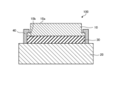
- sample holder that holds samples such as semiconductor wafers to be plasma processed.
- sample holder is constructed by joining a ceramic plate having a sample holding surface to a metal cooling member.
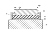
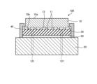
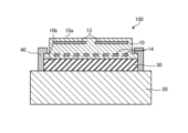
- FIG. 3 is a cross-sectional view schematically showing a sample holder according to another embodiment 1.
- FIG. The sample holder 100 shown in FIG. 3 further includes a bonding material 50.
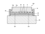
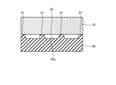
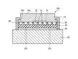
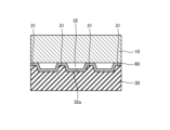
- FIG. 5 is an enlarged view of area A shown in FIG.
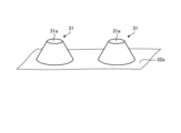
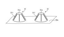
- FIG. 6 is a diagram showing an example of the external configuration of each convex portion shown in FIG. 5.
- each convex portion 31 may be tapered so that the width becomes narrower toward the ceramic plate 10.
- each convex portion 31 may be formed in a tapered shape whose width becomes narrower as it approaches the top of each convex portion 31 .
- the stress generated by the difference in expansion and contraction of can be further alleviated. Further, when the surface roughness Ra of the bottom surface 32a of the space 32 is large, the surface area of the bottom surface 32a of the space 32 can be increased. Thereby, for example, when a heat transfer gas is introduced into the space 32, heat exchange between the heat transfer gas and the heat-resistant member 30 can be promoted.
- FIG. 7 shows the case where the groove 311 is provided on the side surface of each convex portion 31, a protrusion may be provided on the side surface of each convex portion 31 instead of the groove 311. Further, both the groove 311 and the protrusion may be provided on the side surface of each convex portion 31.
- FIG. 8 is a cross-sectional view schematically showing a sample holder according to another third embodiment.
- the ceramic plate 10 has a plurality of convex portions 11 (an example of a second convex portion) in contact with the heat-resistant member 30 on the surface on the heat-resistant member 30 side, that is, the second surface 10b; It has a space 12 (an example of a second space) located around each convex portion 11.
- the plurality of convex portions 11 and spaces 12 can be formed, for example, by blasting the second surface 10b of the ceramic plate 10. Since the ceramic plate 10 has a plurality of convex portions 11 and spaces 12, the contact area between the heat-resistant member 30 and the ceramic plate 10 can be reduced. This allows the ceramic plate 10 to easily slide against the heat-resistant member 30, and it is possible to alleviate stress generated due to the difference in expansion and contraction of the heat-resistant member 30 and the ceramic plate 10 due to thermal cycles.
- Each convex portion 11 may be formed in a tapered shape similarly to each convex portion 31 shown in FIGS. 5 and 6. Furthermore, the surface roughness Ra of the end surface of each convex portion 11 that contacts the heat-resistant member 30 may be smaller than the surface roughness Ra of the bottom surface of the space 12 . Further, each convex portion 11 may have at least one of a protrusion and a groove on the side surface.
- the space 12 is located around each convex portion 11 and between the ceramic plate 10 and the heat-resistant member 30.
- the space 12 has a depth corresponding to the height of each convex portion 11 .
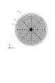
- a heat transfer gas such as helium may be introduced into such space 12, for example. That is, the space 12 may be a flow path for heat transfer gas.
- heat transfer gas may be introduced into the space 12 from a gas supply mechanism (not shown) through the gas introduction hole 121.
- the gas introduction hole 121 penetrates the base member 20, the bonding material 50, and the heat-resistant member 30, and communicates with the space 12.
- the coating layer 60 When the hardness of the coating layer 60 is high, even when frictional force acts on the heat-resistant member 30 due to the difference in thermal expansion between the heat-resistant member 30 and the ceramic plate 10, wear of the heat-resistant member 30 is reduced. , generation of particles from the heat-resistant member 30 can be reduced. If the electrical resistance of the coating layer 60 is small, the charge remaining on the first surface 10a of the ceramic plate 10, that is, the sample holding surface, can be released to the coating layer 60. It is possible to reduce the deterioration in detachability. Further, the coating layer 60 may have a lower electrical resistance than the heat-resistant member 30. Thereby, it is possible to further facilitate the release of charges remaining on the sample holding surface.
- FIG. 12 is a cross-sectional view schematically showing a sample holder according to another embodiment 5.
- two first electrodes 13, 13, which are electrostatic adsorption electrodes that adsorb and hold a sample such as a semiconductor wafer, are located inside the first surface 10a of the ceramic plate 10.
- two second electrodes 14, 14, which are electrostatic adsorption electrodes that adsorb and hold the heat-resistant member 30, may be located inside the ceramic plate 10 on the second surface 10b side.
- the ceramic plate 10 Since the ceramic plate 10 is completely adsorbed to the heat-resistant member 30 including the center, deformation of the first surface 10a, which is the sample holding surface, is reduced, and temperature uniformity within the sample holding surface is improved. Decrease is less likely to occur. In addition, compared to the case where the outer circumferential portion of the ceramic plate 10 is only mechanically fixed, deformation of the first surface 10a, which is the sample holding surface, is reduced, which prevents peeling of the sample from the sample holding surface and machining of the sample. Deterioration in accuracy is also less likely to occur. In this way, the sample holder 100 according to another embodiment 5 can withstand use in a high-temperature environment while reducing deformation of the sample holding surface.
Landscapes
- Physics & Mathematics (AREA)
- Engineering & Computer Science (AREA)
- Plasma & Fusion (AREA)
- Chemical & Material Sciences (AREA)
- Analytical Chemistry (AREA)
- Container, Conveyance, Adherence, Positioning, Of Wafer (AREA)
Priority Applications (4)
| Application Number | Priority Date | Filing Date | Title |
|---|---|---|---|
| US18/851,442 US20250218845A1 (en) | 2022-03-29 | 2023-03-22 | Sample holder |
| CN202380029658.2A CN118843929A (zh) | 2022-03-29 | 2023-03-22 | 试料保持工具 |
| JP2024512238A JP7846750B2 (ja) | 2022-03-29 | 2023-03-22 | 試料保持具 |
| KR1020247030516A KR20240148897A (ko) | 2022-03-29 | 2023-03-22 | 시료 유지구 |
Applications Claiming Priority (2)
| Application Number | Priority Date | Filing Date | Title |
|---|---|---|---|
| JP2022-054579 | 2022-03-29 | ||
| JP2022054579 | 2022-03-29 |
Publications (1)
| Publication Number | Publication Date |
|---|---|
| WO2023189979A1 true WO2023189979A1 (ja) | 2023-10-05 |
Family
ID=88201351
Family Applications (1)
| Application Number | Title | Priority Date | Filing Date |
|---|---|---|---|
| PCT/JP2023/011337 Ceased WO2023189979A1 (ja) | 2022-03-29 | 2023-03-22 | 試料保持具 |
Country Status (5)
| Country | Link |
|---|---|
| US (1) | US20250218845A1 (cg-RX-API-DMAC7.html) |
| JP (1) | JP7846750B2 (cg-RX-API-DMAC7.html) |
| KR (1) | KR20240148897A (cg-RX-API-DMAC7.html) |
| CN (1) | CN118843929A (cg-RX-API-DMAC7.html) |
| WO (1) | WO2023189979A1 (cg-RX-API-DMAC7.html) |
Cited By (2)
| Publication number | Priority date | Publication date | Assignee | Title |
|---|---|---|---|---|
| JP2024047964A (ja) * | 2022-09-27 | 2024-04-08 | 京セラ株式会社 | 試料保持具 |
| WO2026133942A1 (ja) * | 2024-12-19 | 2026-06-25 | 京セラ株式会社 | 試料保持具 |
Citations (6)
| Publication number | Priority date | Publication date | Assignee | Title |
|---|---|---|---|---|
| JPH0917849A (ja) * | 1995-06-28 | 1997-01-17 | Ngk Insulators Ltd | 半導体ウエハー保持装置、その製造方法およびその使用方法 |
| JP2004306254A (ja) * | 2003-03-27 | 2004-11-04 | Ibiden Co Ltd | 真空チャック |
| JP2006339344A (ja) * | 2005-06-01 | 2006-12-14 | Disco Abrasive Syst Ltd | チャックテーブル |
| JP2011159678A (ja) * | 2010-01-29 | 2011-08-18 | Sumitomo Electric Ind Ltd | 静電チャックを備えた基板保持体 |
| JP2013235931A (ja) * | 2012-05-08 | 2013-11-21 | Tanken Seal Seiko Co Ltd | 吸着盤 |
| JP2021034412A (ja) * | 2019-08-16 | 2021-03-01 | 日本特殊陶業株式会社 | 保持装置 |
Family Cites Families (4)
| Publication number | Priority date | Publication date | Assignee | Title |
|---|---|---|---|---|
| US9330953B2 (en) * | 2011-03-23 | 2016-05-03 | Sumitomo Osaka Cement Co., Ltd. | Electrostatic chuck device |
| JP6140457B2 (ja) * | 2013-01-21 | 2017-05-31 | 東京エレクトロン株式会社 | 接着方法、載置台及び基板処理装置 |
| JP6580999B2 (ja) | 2016-01-13 | 2019-09-25 | 日本特殊陶業株式会社 | 保持装置 |
| JP7386086B2 (ja) * | 2020-01-07 | 2023-11-24 | 日本特殊陶業株式会社 | 保持装置 |
-
2023
- 2023-03-22 US US18/851,442 patent/US20250218845A1/en active Pending
- 2023-03-22 CN CN202380029658.2A patent/CN118843929A/zh active Pending
- 2023-03-22 JP JP2024512238A patent/JP7846750B2/ja active Active
- 2023-03-22 WO PCT/JP2023/011337 patent/WO2023189979A1/ja not_active Ceased
- 2023-03-22 KR KR1020247030516A patent/KR20240148897A/ko active Pending
Patent Citations (6)
| Publication number | Priority date | Publication date | Assignee | Title |
|---|---|---|---|---|
| JPH0917849A (ja) * | 1995-06-28 | 1997-01-17 | Ngk Insulators Ltd | 半導体ウエハー保持装置、その製造方法およびその使用方法 |
| JP2004306254A (ja) * | 2003-03-27 | 2004-11-04 | Ibiden Co Ltd | 真空チャック |
| JP2006339344A (ja) * | 2005-06-01 | 2006-12-14 | Disco Abrasive Syst Ltd | チャックテーブル |
| JP2011159678A (ja) * | 2010-01-29 | 2011-08-18 | Sumitomo Electric Ind Ltd | 静電チャックを備えた基板保持体 |
| JP2013235931A (ja) * | 2012-05-08 | 2013-11-21 | Tanken Seal Seiko Co Ltd | 吸着盤 |
| JP2021034412A (ja) * | 2019-08-16 | 2021-03-01 | 日本特殊陶業株式会社 | 保持装置 |
Cited By (2)
| Publication number | Priority date | Publication date | Assignee | Title |
|---|---|---|---|---|
| JP2024047964A (ja) * | 2022-09-27 | 2024-04-08 | 京セラ株式会社 | 試料保持具 |
| WO2026133942A1 (ja) * | 2024-12-19 | 2026-06-25 | 京セラ株式会社 | 試料保持具 |
Also Published As
| Publication number | Publication date |
|---|---|
| JPWO2023189979A1 (cg-RX-API-DMAC7.html) | 2023-10-05 |
| JP7846750B2 (ja) | 2026-04-15 |
| CN118843929A (zh) | 2024-10-25 |
| US20250218845A1 (en) | 2025-07-03 |
| KR20240148897A (ko) | 2024-10-11 |
Similar Documents
| Publication | Publication Date | Title |
|---|---|---|
| CN111480222B (zh) | 静电卡盘装置及静电卡盘装置的制造方法 | |
| TWI688038B (zh) | 局部加熱之多區域基材支撐座 | |
| TWI705520B (zh) | 用於高溫製程之基板支撐組件 | |
| CN110767596B (zh) | 静电吸盘 | |
| CN103733327B (zh) | 具有加热器的基板支撑件 | |
| CN103370778B (zh) | 具有加热器与快速温度变化的基板支撑件 | |
| JP7846750B2 (ja) | 試料保持具 | |
| CN111512428A (zh) | 静电卡盘装置 | |
| JP2020080365A (ja) | ウェハーステージ、半導体製造装置、ウェハーステージの製造方法 | |
| US11309203B2 (en) | Wafer stage and method of manufacturing the same | |
| JPWO2023189979A5 (cg-RX-API-DMAC7.html) | ||
| WO2023286812A1 (ja) | 静電チャック | |
| JP7862530B2 (ja) | 試料保持具 | |
| WO2023189954A1 (ja) | 試料保持具 | |
| JP7604872B2 (ja) | 静電チャック装置 | |
| WO2024154758A1 (ja) | 静電チャック | |
| JP2024047964A (ja) | 試料保持具 | |
| JP6642170B2 (ja) | 静電チャック装置及びその製造方法 | |
| JP2013042049A (ja) | ウェハ支持装置 | |
| JP7742945B1 (ja) | サセプタ | |
| WO2025154609A1 (ja) | 試料保持具 | |
| CN114402427A (zh) | 可偏转压板以及相关方法 | |
| WO2025047725A1 (ja) | 試料保持具 | |
| JP2025089772A (ja) | 試料保持具 | |
| KR102896960B1 (ko) | 유지 장치 |
Legal Events
| Date | Code | Title | Description |
|---|---|---|---|
| 121 | Ep: the epo has been informed by wipo that ep was designated in this application |
Ref document number: 23779991 Country of ref document: EP Kind code of ref document: A1 |
|
| ENP | Entry into the national phase |
Ref document number: 20247030516 Country of ref document: KR Kind code of ref document: A |
|
| WWE | Wipo information: entry into national phase |
Ref document number: 1020247030516 Country of ref document: KR |
|
| ENP | Entry into the national phase |
Ref document number: 2024512238 Country of ref document: JP Kind code of ref document: A |
|
| WWE | Wipo information: entry into national phase |
Ref document number: 202380029658.2 Country of ref document: CN |
|
| WWE | Wipo information: entry into national phase |
Ref document number: 18851442 Country of ref document: US |
|
| NENP | Non-entry into the national phase |
Ref country code: DE |
|
| 122 | Ep: pct application non-entry in european phase |
Ref document number: 23779991 Country of ref document: EP Kind code of ref document: A1 |
|
| WWP | Wipo information: published in national office |
Ref document number: 18851442 Country of ref document: US |