WO2023189754A1 - Dispositif à semi-conducteur - Google Patents
Dispositif à semi-conducteur Download PDFInfo
- Publication number
- WO2023189754A1 WO2023189754A1 PCT/JP2023/010676 JP2023010676W WO2023189754A1 WO 2023189754 A1 WO2023189754 A1 WO 2023189754A1 JP 2023010676 W JP2023010676 W JP 2023010676W WO 2023189754 A1 WO2023189754 A1 WO 2023189754A1
- Authority
- WO
- WIPO (PCT)
- Prior art keywords
- region
- boundary
- semiconductor device
- chip
- cathode
- Prior art date
Links
- 239000004065 semiconductor Substances 0.000 title claims abstract description 187
- 239000002344 surface layer Substances 0.000 claims abstract description 57
- 239000011229 interlayer Substances 0.000 claims description 75
- 230000000149 penetrating effect Effects 0.000 claims 1
- 238000002955 isolation Methods 0.000 description 92
- 230000002093 peripheral effect Effects 0.000 description 80
- 229910052751 metal Inorganic materials 0.000 description 50
- 239000002184 metal Substances 0.000 description 50
- 108091006146 Channels Proteins 0.000 description 25
- 239000012535 impurity Substances 0.000 description 23
- 230000004048 modification Effects 0.000 description 12
- 238000012986 modification Methods 0.000 description 12
- VYPSYNLAJGMNEJ-UHFFFAOYSA-N Silicium dioxide Chemical compound O=[Si]=O VYPSYNLAJGMNEJ-UHFFFAOYSA-N 0.000 description 8
- 238000005192 partition Methods 0.000 description 8
- 229910052814 silicon oxide Inorganic materials 0.000 description 8
- 239000000969 carrier Substances 0.000 description 7
- 230000003247 decreasing effect Effects 0.000 description 7
- XUIMIQQOPSSXEZ-UHFFFAOYSA-N Silicon Chemical compound [Si] XUIMIQQOPSSXEZ-UHFFFAOYSA-N 0.000 description 6
- 230000000694 effects Effects 0.000 description 6
- 229910052710 silicon Inorganic materials 0.000 description 6
- 239000010703 silicon Substances 0.000 description 6
- 239000002356 single layer Substances 0.000 description 5
- 239000000758 substrate Substances 0.000 description 5
- 229910052581 Si3N4 Inorganic materials 0.000 description 4
- 230000005684 electric field Effects 0.000 description 4
- TWNQGVIAIRXVLR-UHFFFAOYSA-N oxo(oxoalumanyloxy)alumane Chemical compound O=[Al]O[Al]=O TWNQGVIAIRXVLR-UHFFFAOYSA-N 0.000 description 4
- HQVNEWCFYHHQES-UHFFFAOYSA-N silicon nitride Chemical compound N12[Si]34N5[Si]62N3[Si]51N64 HQVNEWCFYHHQES-UHFFFAOYSA-N 0.000 description 4
- 229910045601 alloy Inorganic materials 0.000 description 3
- 239000000956 alloy Substances 0.000 description 3
- 239000013078 crystal Substances 0.000 description 3
- 229910021420 polycrystalline silicon Inorganic materials 0.000 description 3
- 229920005591 polysilicon Polymers 0.000 description 3
- 239000005368 silicate glass Substances 0.000 description 3
- 229910000838 Al alloy Inorganic materials 0.000 description 2
- 229910001069 Ti alloy Inorganic materials 0.000 description 2
- 239000004020 conductor Substances 0.000 description 2
- 239000010410 layer Substances 0.000 description 2
- HBMJWWWQQXIZIP-UHFFFAOYSA-N silicon carbide Chemical compound [Si+]#[C-] HBMJWWWQQXIZIP-UHFFFAOYSA-N 0.000 description 2
- 229910010271 silicon carbide Inorganic materials 0.000 description 2
- 229910016570 AlCu Inorganic materials 0.000 description 1
- 229910000789 Aluminium-silicon alloy Inorganic materials 0.000 description 1
- 229910000881 Cu alloy Inorganic materials 0.000 description 1
- 102000004129 N-Type Calcium Channels Human genes 0.000 description 1
- 108090000699 N-Type Calcium Channels Proteins 0.000 description 1
- OAICVXFJPJFONN-UHFFFAOYSA-N Phosphorus Chemical compound [P] OAICVXFJPJFONN-UHFFFAOYSA-N 0.000 description 1
- ATJFFYVFTNAWJD-UHFFFAOYSA-N Tin Chemical compound [Sn] ATJFFYVFTNAWJD-UHFFFAOYSA-N 0.000 description 1
- 229910001080 W alloy Inorganic materials 0.000 description 1
- GDFCWFBWQUEQIJ-UHFFFAOYSA-N [B].[P] Chemical compound [B].[P] GDFCWFBWQUEQIJ-UHFFFAOYSA-N 0.000 description 1
- 238000009825 accumulation Methods 0.000 description 1
- 210000000746 body region Anatomy 0.000 description 1
- 230000015556 catabolic process Effects 0.000 description 1
- 230000006866 deterioration Effects 0.000 description 1
- 238000010586 diagram Methods 0.000 description 1
- 238000000926 separation method Methods 0.000 description 1
Images


Classifications
-
- H—ELECTRICITY
- H01—ELECTRIC ELEMENTS
- H01L—SEMICONDUCTOR DEVICES NOT COVERED BY CLASS H10
- H01L29/00—Semiconductor devices specially adapted for rectifying, amplifying, oscillating or switching and having potential barriers; Capacitors or resistors having potential barriers, e.g. a PN-junction depletion layer or carrier concentration layer; Details of semiconductor bodies or of electrodes thereof ; Multistep manufacturing processes therefor
- H01L29/02—Semiconductor bodies ; Multistep manufacturing processes therefor
- H01L29/06—Semiconductor bodies ; Multistep manufacturing processes therefor characterised by their shape; characterised by the shapes, relative sizes, or dispositions of the semiconductor regions ; characterised by the concentration or distribution of impurities within semiconductor regions
-
- H—ELECTRICITY
- H01—ELECTRIC ELEMENTS
- H01L—SEMICONDUCTOR DEVICES NOT COVERED BY CLASS H10
- H01L29/00—Semiconductor devices specially adapted for rectifying, amplifying, oscillating or switching and having potential barriers; Capacitors or resistors having potential barriers, e.g. a PN-junction depletion layer or carrier concentration layer; Details of semiconductor bodies or of electrodes thereof ; Multistep manufacturing processes therefor
- H01L29/02—Semiconductor bodies ; Multistep manufacturing processes therefor
- H01L29/12—Semiconductor bodies ; Multistep manufacturing processes therefor characterised by the materials of which they are formed
-
- H—ELECTRICITY
- H01—ELECTRIC ELEMENTS
- H01L—SEMICONDUCTOR DEVICES NOT COVERED BY CLASS H10
- H01L29/00—Semiconductor devices specially adapted for rectifying, amplifying, oscillating or switching and having potential barriers; Capacitors or resistors having potential barriers, e.g. a PN-junction depletion layer or carrier concentration layer; Details of semiconductor bodies or of electrodes thereof ; Multistep manufacturing processes therefor
- H01L29/66—Types of semiconductor device ; Multistep manufacturing processes therefor
- H01L29/68—Types of semiconductor device ; Multistep manufacturing processes therefor controllable by only the electric current supplied, or only the electric potential applied, to an electrode which does not carry the current to be rectified, amplified or switched
- H01L29/70—Bipolar devices
- H01L29/72—Transistor-type devices, i.e. able to continuously respond to applied control signals
- H01L29/739—Transistor-type devices, i.e. able to continuously respond to applied control signals controlled by field-effect, e.g. bipolar static induction transistors [BSIT]
-
- H—ELECTRICITY
- H01—ELECTRIC ELEMENTS
- H01L—SEMICONDUCTOR DEVICES NOT COVERED BY CLASS H10
- H01L29/00—Semiconductor devices specially adapted for rectifying, amplifying, oscillating or switching and having potential barriers; Capacitors or resistors having potential barriers, e.g. a PN-junction depletion layer or carrier concentration layer; Details of semiconductor bodies or of electrodes thereof ; Multistep manufacturing processes therefor
- H01L29/66—Types of semiconductor device ; Multistep manufacturing processes therefor
- H01L29/68—Types of semiconductor device ; Multistep manufacturing processes therefor controllable by only the electric current supplied, or only the electric potential applied, to an electrode which does not carry the current to be rectified, amplified or switched
- H01L29/76—Unipolar devices, e.g. field effect transistors
- H01L29/772—Field effect transistors
- H01L29/78—Field effect transistors with field effect produced by an insulated gate
-
- H—ELECTRICITY
- H01—ELECTRIC ELEMENTS
- H01L—SEMICONDUCTOR DEVICES NOT COVERED BY CLASS H10
- H01L29/00—Semiconductor devices specially adapted for rectifying, amplifying, oscillating or switching and having potential barriers; Capacitors or resistors having potential barriers, e.g. a PN-junction depletion layer or carrier concentration layer; Details of semiconductor bodies or of electrodes thereof ; Multistep manufacturing processes therefor
- H01L29/66—Types of semiconductor device ; Multistep manufacturing processes therefor
- H01L29/86—Types of semiconductor device ; Multistep manufacturing processes therefor controllable only by variation of the electric current supplied, or only the electric potential applied, to one or more of the electrodes carrying the current to be rectified, amplified, oscillated or switched
- H01L29/861—Diodes
- H01L29/868—PIN diodes
Definitions
- Patent Document 1 discloses a semiconductor device including an RC-IGBT (Reverse Conducting - Insulating Gate Bipolar Transistor).
- RC-IGBT Reverse Conducting - Insulating Gate Bipolar Transistor
- One embodiment provides a semiconductor device that contributes to improved electrical characteristics.
- One embodiment includes a chip having a first surface on one side and a second surface on the other side, a plurality of IGBT regions provided at intervals on the chip, and a plurality of IGBT regions between the plurality of IGBT regions in the chip. a boundary region provided in the boundary region, a first conductivity type cathode region formed in the surface layer portion of the second surface in the boundary region, and a second conductivity type cathode region formed in the surface layer portion of the first surface in the boundary region.
- a semiconductor device is provided, including a conductive type well region.
- One embodiment includes a chip having a first surface on one side and a second surface on the other side, a plurality of IGBT regions provided at intervals on the chip, and a plurality of IGBT regions between the plurality of IGBT regions in the chip. a boundary region provided in the boundary region, a first conductivity type cathode region formed in the surface layer portion of the second surface in the boundary region, and a second conductivity type cathode region formed in the surface layer portion of the first surface in the boundary region.
- a semiconductor device including an emitter electrode disposed on the interlayer insulating film so as to be electrically connected to the via electrode.
- One embodiment includes a chip having a first main surface on one side and a second main surface on the other side, a plurality of IGBT regions set on the first main surface, and a plurality of IGBT regions set on the first main surface. a boundary region set between the regions, an outer peripheral region set around the plurality of IGBT regions on the first main surface, an IGBT structure formed in each of the IGBT regions, and an IGBT structure formed in the boundary region. and an outer diode formed in the outer peripheral region.
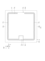
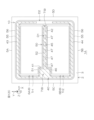
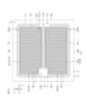
- FIG. 1 is a plan view showing a semiconductor device according to a first embodiment.
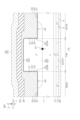
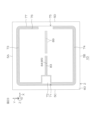
- FIG. 2 is a plan view showing an example layout of a plurality of IGBT regions, boundary regions, gate electrodes, and emitter electrodes.
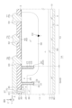
- FIG. 3 is a plan view showing a layout example of the gate wiring, the boundary cathode region, the boundary well region, the outer well region, and the outer cathode region.
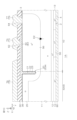
- FIG. 4 is an enlarged plan view showing an example layout of a plurality of IGBT regions and a boundary region.
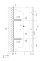
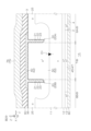
- FIG. 5 is a sectional view taken along the line V-V shown in FIG. 4.
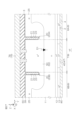
- FIG. 6 is a cross-sectional view taken along line VI-VI shown in FIG. 4.
- FIG. 5 is a sectional view taken along the line V-V shown in FIG. 4.
- FIG. 6 is a cross-sectional view taken along line VI-VI shown in FIG. 4.
- FIG. 5 is a sectional view taken along the line V-V shown in FIG. 4.
- FIG. 7 is a sectional view taken along line VII-VII shown in FIG. 4.
- FIG. 8 is an enlarged plan view showing an example of the layout of the peripheral portion of the IGBT region.
- FIG. 9 is a sectional view taken along line IX-IX shown in FIG. 8.
- FIG. 10 is a cross-sectional view taken along the line XX shown in FIG. 8.
- FIG. 11 is a cross-sectional view showing the peripheral edge of the chip.
- FIG. 12A is a plan view showing another example of the layout of the cathode region.
- FIG. 12B is a plan view showing another example of the layout of the cathode region.
- FIG. 12C is a plan view showing another example of the layout of the cathode region.
- FIG. 12A is a plan view showing another example of the layout of the cathode region.
- FIG. 12B is a plan view showing another example of the layout of the cathode region.
- FIG. 12C is a plan
- FIG. 12D is a plan view showing another example of the layout of the cathode region.
- FIG. 12E is a plan view showing another example of the layout of the cathode region.
- FIG. 12F is a plan view showing another example of the layout of the cathode region.
- FIG. 12G is a plan view showing another example of the layout of the cathode region.
- FIG. 12H is a plan view showing another example of the layout of the cathode region.
- FIG. 12I is a plan view showing another example of the layout of the cathode region.
- FIG. 12J is a plan view showing another example of the layout of the cathode region.
- FIG. 12K is a plan view showing another example of the layout of the cathode region.
- FIG. 12L is a plan view showing another example of the layout of the cathode region.
- FIG. 12M is a plan view showing another example of the layout of the cathode region.
- FIG. 12N is a plan view showing another example of the layout of the cathode region.
- FIG. 13 is a plan view showing the layout of a semiconductor device according to a reference example.
- FIG. 14 is a graph showing the relationship between peak surge current and forward voltage.
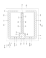
- FIG. 15 is a plan view showing a semiconductor device according to the second embodiment.
- FIG. 16 is a plan view showing an example layout of a plurality of IGBT regions, boundary regions, gate electrodes, and emitter electrodes.
- FIG. 17 is an enlarged plan view showing a layout example of a plurality of IGBT regions and a boundary region.
- FIG. 18 is a sectional view taken along the line XVIII-XVIII shown in FIG. 17.
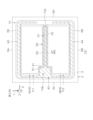
- FIG. 19 is a plan view showing a semiconductor device according to a third embodiment.
- FIG. 20 is a plan view showing an example layout of a plurality of IGBT regions, boundary regions, gate electrodes, and emitter electrodes.
- FIG. 21 is an enlarged plan view showing a layout example of a plurality of IGBT regions and a boundary region.
- FIG. 22 is a sectional view taken along the line XXII-XXII shown in FIG. 21.
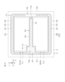
- FIG. 23 is a plan view showing a semiconductor device according to a fourth embodiment.
- FIG. 24 is a plan view showing an example layout of a plurality of IGBT regions, boundary regions, gate electrodes, and emitter electrodes.
- FIG. 25 is an enlarged plan view showing a layout example of a plurality of IGBT regions and a boundary region.
- FIG. 26 is a cross-sectional view showing a main part of the semiconductor device according to the fifth embodiment.
- FIG. 27 is a sectional view showing a main part of a semiconductor device according to a sixth embodiment.
- FIG. 28 is a plan view showing a modification applied to each of the embodiments described above.
- FIG. 29 is a plan view showing a modification applied to each of the embodiments described above.
- FIG. 30 is a plan view showing a modification applied to each of the embodiments described above.
- this phrase includes a numerical value (form) that is equal to the numerical value (form) of the comparison target; It also includes a numerical error (form error) in the range of ⁇ 10% based on (form).
- a numerical value that is equal to the numerical value (form) of the comparison target
- a numerical error form error in the range of ⁇ 10% based on (form).
- words such as “first”, “second”, “third”, etc. are used, but these are symbols attached to the name of each structure to clarify the order of explanation; It is not given for the purpose of limiting the name.
- FIG. 1 is a plan view showing a semiconductor device 1A according to the first embodiment.
- FIG. 2 is a plan view showing an example of the layout of a plurality of IGBT regions 6, boundary regions 7, gate electrodes 71, and emitter electrodes 75.
- FIG. 3 is a plan view showing an example layout of the gate wiring 40, the boundary cathode region 45, the boundary well region 50, the outer cathode region 55, and the outer well region 56.
- FIG. 4 is an enlarged plan view showing a layout example of the plurality of IGBT regions 6 and the boundary region 7. As shown in FIG.
- FIG. 5 is a cross-sectional view taken along the line V-V shown in FIG. 4.
- FIG. 6 is a cross-sectional view taken along line VI-VI shown in FIG. 4.
- FIG. 7 is a sectional view taken along line VII-VII shown in FIG. 4.
- FIG. 8 is an enlarged plan view showing a layout example of the peripheral portion of the IGBT region 6.
- FIG. 9 is a sectional view taken along line IX-IX shown in FIG. 8.
- FIG. 10 is a cross-sectional view taken along the line XX shown in FIG. 8.
- FIG. 11 is a cross-sectional view showing the peripheral portion of the chip 2. As shown in FIG.
- a semiconductor device 1A is an RC-IGBT semiconductor device (semiconductor switching device) having an RC-IGBT (Reverse Conducting - IGBT) integrally equipped with an IGBT (Insulated Gate Bipolar Transistor) and a diode. ).
- the diode is a freewheeling diode for the IGBT.
- the semiconductor device 1A includes a chip 2 having a hexahedral shape (specifically, a rectangular parallelepiped shape).
- Chip 2 may also be referred to as a "semiconductor chip.”
- the chip 2 has a single layer structure made of a silicon single crystal substrate (semiconductor substrate).
- the chip 2 has a first main surface 3 on one side, a second main surface 4 on the other side, and first to fourth side surfaces 5A to 5D connecting the first main surface 3 and the second main surface 4. ing.
- the first main surface 3 and the second main surface 4 are formed into a rectangular shape in a plan view (hereinafter simply referred to as "plan view") when viewed from the normal direction Z thereof.
- the normal direction Z is also the thickness direction of the chip 2.
- the first side face 5A and the second side face 5B extend in a first direction
- the third side surface 5C and the fourth side surface 5D extend in the second direction Y and face the first direction X.
- the semiconductor device 1A includes a plurality of IGBT regions 6 provided at intervals on the chip 2.
- Each IGBT region 6 is a region having an IGBT structure, and may be referred to as an "active region.”
- the multiple IGBT regions 6 include a first IGBT region 6A and a second IGBT region 6B.
- the first IGBT region 6A is provided in a region on the first side surface 5A side with respect to a straight line that crosses the center of the first main surface 3 in the first direction X.
- the second IGBT region 6B is provided in a region on the second side surface 5B side with respect to a straight line that crosses the center of the first main surface 3 in the first direction X.
- the plurality of IGBT regions 6 are each formed in a polygonal shape having four sides parallel to the first to fourth side surfaces 5A to 5D in plan view.
- the semiconductor device 1A includes a boundary region 7 provided in a region between a plurality of IGBT regions 6.
- the boundary region 7 is provided in a band shape extending in the first direction X in the region between the first IGBT region 6A and the second IGBT region 6B.
- the boundary region 7 is located on a straight line that crosses the center of the first main surface 3 in the first direction X.
- the boundary region 7 includes a first region 8 having a relatively large first width in the second direction Y, and a second region 9 having a second width smaller than the first width in the second direction Y.
- the first region 8 is provided on one side (the third side surface 5C side) in the first direction X as a portion that supports the terminal electrode.
- the first region 8 may also be referred to as a "pad region,” "wide region,” or "terminal support region.”
- the first region 8 is located on a straight line that crosses the center of the first main surface 3 in the first direction X in plan view, and is provided in a quadrangular shape near the center of the third side surface 5C.
- the first width of the first region 8 may be 100 ⁇ m or more and 800 ⁇ m or less.
- the first width is preferably 200 ⁇ m or more and 600 ⁇ m or less.
- the first width is set in a range of 350 ⁇ m or more and 450 ⁇ m or less.
- the second region 9 is provided on the other side (the fourth side surface 5D side) of the first region 8 in the first direction X as a portion that supports the wiring.
- the second region 9 is located on a straight line that crosses the center of the first main surface 3 in the first direction X, and is drawn out in a band shape from the first region 8 toward the center of the fourth side surface 5D.
- the second region 9 may be referred to as a "street region,” a "narrow region,” or a "wiring support region.”
- the second width of the second region 9 may be 0.1 ⁇ m or more and 500 ⁇ m or less.
- the second width is preferably 100 ⁇ m or less.
- the second width is 0.1 ⁇ m or more and 0.5 ⁇ m or less, 0.5 ⁇ m or more and 1 ⁇ m or less, 1 ⁇ m or more and 5 ⁇ m or less, 5 ⁇ m or more and 10 ⁇ m or less, 10 ⁇ m or more and 25 ⁇ m or less, 25 ⁇ m or more and 50 ⁇ m or less, 50 ⁇ m or more and 75 ⁇ m or less, and 75 ⁇ m or more. It may be set to a value belonging to any range of 100 ⁇ m or less.
- the semiconductor device 1A includes an outer peripheral region 10 provided at the peripheral edge of the chip 2 so as to collectively surround the plurality of IGBT regions 6.
- the outer peripheral region 10 is provided in an annular shape (square annular shape) extending along the first to fourth side surfaces 5A to 5D.
- the semiconductor device 1A includes an n-type (first conductivity type) drift region 11 formed inside the chip 2.
- Drift region 11 is formed throughout the interior of chip 2 .
- the chip 2 is made of an n-type semiconductor substrate (n-type semiconductor chip), and the drift region 11 is formed using the chip 2.
- the semiconductor device 1A includes an n-type buffer region 12 formed in the surface layer portion of the second main surface 4.
- the buffer region 12 is formed in a layered manner extending along the second main surface 4 over the entire second main surface 4 .
- Buffer region 12 has a higher n-type impurity concentration than drift region 11 .
- the presence or absence of the buffer area 12 is arbitrary, and a configuration without the buffer area 12 may be adopted.
- the semiconductor device 1A includes a p-type (second conductivity type) collector region 13 formed in the surface layer portion of the second main surface 4.
- the collector region 13 is formed in the surface layer portion of the buffer region 12 on the second main surface 4 side.
- the collector region 13 is formed in a layered shape extending along the second main surface 4 over the entire second main surface 4 .
- the collector region 13 is exposed from part of the second main surface 4 and the first to fourth side surfaces 5A to 5D.
- the semiconductor device 1A includes a plurality of trench isolation structures 20 formed on the first main surface 3 to partition a plurality of IGBT regions 6. A gate potential is applied to the plurality of trench isolation structures 20 .
- Trench isolation structure 20 may be referred to as a "trench gate isolation structure” or a "trench gate connection structure.”
- the plurality of trench isolation structures 20 include a first trench isolation structure 20A that defines the first IGBT region 6A, and a second trench isolation structure 20B that defines the second IGBT region 6B.
- the first trench isolation structure 20A surrounds the first IGBT region 6A and partitions the first IGBT region 6A from the boundary region 7 and the outer peripheral region 10.
- the first trench isolation structure 20A is formed into a polygonal ring shape having four sides parallel to the first to fourth side surfaces 5A to 5D in plan view.
- the second trench isolation structure 20B surrounds the second IGBT region 6B and partitions the second IGBT region 6B from the boundary region 7 and the outer peripheral region 10.
- the second trench isolation structure 20B is formed into a polygonal ring shape having four sides parallel to the first to fourth side surfaces 5A to 5D in plan view.
- the plurality of trench isolation structures 20 each have a bent portion so as to partition the first region 8 and the second region 9 of the boundary region 7 in plan view.
- each trench isolation structure 20 has a width less than the width of the second region 9 of the boundary region 7 .
- each trench isolation structure 20 may be 0.5 ⁇ m or more and 5 ⁇ m or less.
- the width of each trench isolation structure 20 is preferably 1 ⁇ m or more and 2.5 ⁇ m or less.
- Each trench isolation structure 20 may have a depth of 1 ⁇ m or more and 20 ⁇ m or less.
- the depth of each trench isolation structure 20 is preferably 4 ⁇ m or more and 10 ⁇ m or less.
- Trench isolation structure 20 includes an isolation trench 21 , an isolation insulating film 22 , and an isolation buried electrode 23 .
- the isolation trench 21 is dug down from the first main surface 3 toward the second main surface 4 and partitions the wall surface of the trench isolation structure 20.
- the isolation insulating film 22 is formed in a film shape along the wall surface of the isolation trench 21 and defines a recess space within the isolation trench 21 .
- the isolation insulating film 22 may include at least one of a silicon oxide film, a silicon nitride film, a silicon oxynitride film, and an aluminum oxide film. It is preferable that the isolation insulating film 22 has a single layer structure consisting of a single insulating film. It is particularly preferable that the isolation insulating film 22 includes a silicon oxide film made of an oxide of the chip 2 .
- the isolation buried electrode 23 is buried in the isolation trench 21 with the isolation insulating film 22 in between.
- the separate buried electrode 23 is made of conductive polysilicon. A gate potential is applied to the separated buried electrode 23.
- the structure on the second IGBT region 6B side is almost the same as the structure on the first IGBT region 6A side. Specifically, the structure on the second IGBT region 6B side is line symmetrical to the structure on the first IGBT region 6A side with respect to the boundary region 7. Below, the structure on the first IGBT region 6A side will be explained. Regarding the description of the structure on the second IGBT region 6B side, the description of the structure on the first IGBT region 6A side is applied and will be omitted.
- the semiconductor device 1A includes a p-type base region 25 formed in the surface layer portion of the first main surface 3 in the first IGBT region 6A.
- Base region 25 may be referred to as a "body region” or a "channel region.”
- the base region 25 is formed at a depth shallower than the trench isolation structure 20 and has a bottom portion located closer to the first main surface 3 than the bottom wall of the trench isolation structure 20 .
- the base region 25 extends in a layered manner along the first main surface 3 and is connected to the inner peripheral wall of the trench isolation structure 20 .
- the semiconductor device 1A includes a plurality of trench structures 30 formed on the first main surface 3 in the first IGBT region 6A.
- a gate potential is applied to the plurality of trench structures 30 .
- Trench structure 30 may be referred to as a "trench gate structure.”
- a plurality of trench structures 30 penetrate base region 25 to reach drift region 11 .
- the plurality of trench structures 30 are arranged at intervals in the first direction X in a plan view, and are each formed in a band shape extending in the second direction Y. That is, the plurality of trench structures 30 are arranged in stripes extending in the second direction Y.
- the plurality of trench structures 30 each have a first end 30A on the boundary region 7 side and a second end 30B on the outer peripheral region 10 side in the longitudinal direction (second direction Y).
- the first end 30A and the second end 30B are mechanically and electrically connected to the trench isolation structure 20.
- the plurality of trench structures 30 together with the trench isolation structure 20 constitute one ladder-like trench gate structure.
- the connection between trench structure 30 and trench isolation structure 20 may be considered as part of trench isolation structure 20 or may be considered as part of trench structure 30.
- the plurality of trench structures 30 may be arranged in the first direction X at intervals of 0.5 ⁇ m or more and 5 ⁇ m or less.
- the interval between the plurality of trench structures 30 is preferably 1 ⁇ m or more and 3 ⁇ m or less.
- the spacing between the plurality of trench structures 30 is less than the width of the second region 9 of the boundary region 7 .
- Each trench structure 30 may have a width of 0.5 ⁇ m or more and 5 ⁇ m or less.
- the width of each trench structure 30 is the width in a direction perpendicular to the direction in which each trench structure 30 extends.
- the width of each trench structure 30 is preferably 1 ⁇ m or more and 2.5 ⁇ m or less.
- the width of each trench structure 30 is less than the width of the second region 9 of the boundary region 7.
- the width of each trench structure 30 is approximately equal to the width of trench isolation structure 20.
- Each trench structure 30 may have a depth of 1 ⁇ m or more and 20 ⁇ m or less.
- the depth of each trench structure 30 is preferably 4 ⁇ m or more and 10 ⁇ m or less.
- the depth of each trench structure 30 is approximately equal to the depth of trench isolation structure 20.
- Trench structure 30 includes a gate trench 31, a gate insulating film 32, and a gate buried electrode 33.
- the gate trench 31 is dug down from the first main surface 3 toward the second main surface 4 and partitions the wall surface of the trench structure 30.
- the gate trench 31 communicates with the isolation trench 21 at both ends (first end 30A and second end 30B) in the second direction Y.
- the side wall of the gate trench 31 communicates with the side wall of the isolation trench 21, and the bottom wall of the gate trench 31 communicates with the bottom wall of the isolation trench 21.
- the gate insulating film 32 is formed in a film shape along the wall surface of the gate trench 31, and defines a recess space within the gate trench 31.
- the gate insulating film 32 may include at least one of a silicon oxide film, a silicon nitride film, a silicon oxynitride film, and an aluminum oxide film.
- the gate insulating film 32 has a single layer structure consisting of a single insulating film. It is particularly preferable that the gate insulating film 32 includes a silicon oxide film made of the oxide of the chip 2. In this embodiment, the gate insulating film 32 is made of the same insulating film as the isolation insulating film 22. Gate insulating film 32 is connected to isolation insulating film 22 at a communication portion between isolation trench 21 and gate trench 31 .
- the gate buried electrode 33 is buried in the gate trench 31 with the gate insulating film 32 in between.
- the gate buried electrode 33 is made of conductive polysilicon.
- a gate potential is applied to the gate buried electrode 33.
- the gate buried electrode 33 is connected to the separated buried electrode 23 at a communication portion between the separated trench 21 and the gate trench 31 .
- the semiconductor device 1A includes a plurality of n-type emitter regions 35 formed in the surface layer of the base region 25.
- the plurality of emitter regions 35 are arranged on both sides of the plurality of trench structures 30 and are each formed in a band shape extending along the plurality of trench structures 30 in plan view.
- Each of the plurality of emitter regions 35 has a higher n-type impurity concentration than the drift region 11.
- the semiconductor device 1A includes a plurality of n-type carrier storage regions 36 formed in a region immediately below the base region 25 within the chip 2.
- the plurality of carrier storage regions 36 suppress the discharge of carriers (holes) to the base region 25 and promote accumulation of carriers (holes) in the region directly under the plurality of trench structures 30 .
- the plurality of carrier storage regions 36 promotes lower on-resistance and lower on-voltage from the inside of the chip 2.
- the plurality of carrier storage regions 36 are arranged on both sides of the plurality of trench structures 30 and are each formed in a band shape extending along the plurality of trench structures 30 in plan view.
- a plurality of carrier storage regions 36 are each formed in a region between the bottom of the base region 25 and the bottom wall of the trench structure 30 in the thickness direction of the chip 2.
- the plurality of carrier storage regions 36 are spaced apart from the bottom wall of the trench structure 30 toward the base region 25 .
- the bottoms of the plurality of carrier storage regions 36 are preferably located closer to the bottom wall of the trench structure 30 than the middle part of the trench structure 30.
- the plurality of carrier storage regions 36 have a higher n-type impurity concentration than the drift region 11.
- the n-type impurity concentration of the plurality of carrier storage regions 36 is preferably lower than that of the emitter region 35.
- the presence or absence of the carrier storage area 36 is optional. Therefore, a configuration without the carrier storage area 36 may be adopted.
- the semiconductor device 1A includes a plurality of contact holes 37 formed in the first main surface 3 so as to expose the emitter region 35.
- the plurality of contact holes 37 are formed on both sides of the plurality of trench structures 30 at intervals in the first direction X from the plurality of trench structures 30 .
- the plurality of contact holes 37 may each be formed in a tapered shape in which the opening width narrows from the opening toward the bottom wall.
- the plurality of contact holes 37 may be spaced apart from the bottom of the emitter region 35 toward the first main surface 3 so as not to reach the base region 25. Of course, the plurality of contact holes 37 may extend through the emitter region 35 to reach the base region 25.
- the plurality of contact holes 37 are each formed in a band shape extending along the plurality of trench structures 30 in plan view. The plurality of contact holes 37 are shorter than the plurality of trench structures 30 in the longitudinal direction (second direction Y).
- the semiconductor device 1A includes a plurality of p-type contact regions 38 formed in a region different from the plurality of emitter regions 35 in the surface layer portion of the base region 25.
- the plurality of contact regions 38 are each formed in a band shape extending along the corresponding contact hole 37 in plan view.
- the bottoms of the plurality of contact regions 38 are each formed in a region between the bottom wall of the corresponding contact hole 37 and the bottom of the base region 25 .
- the plurality of contact regions 38 have a higher p-type impurity concentration than the base region 25.
- the first IGBT region 6A includes a base region 25, a plurality of trench structures 30, a plurality of emitter regions 35, a plurality of carrier storage regions 36, a plurality of contact holes 37, and a plurality of contact regions 38.
- the second IGBT region 6B like the first IGBT region 6A, includes a base region 25, a plurality of trench structures 30, a plurality of emitter regions 35, a plurality of carrier storage regions 36, a plurality of contact holes 37, and a plurality of contact regions 38. .
- the semiconductor device 1A includes a main surface insulating film 39 that covers the first main surface 3.
- Main surface insulating film 39 may include at least one of a silicon oxide film, a silicon nitride film, a silicon oxynitride film, and an aluminum oxide film. It is preferable that the main surface insulating film 39 has a single layer structure consisting of a single insulating film. It is particularly preferable that the main surface insulating film 39 includes a silicon oxide film made of an oxide of the chip 2 . In this embodiment, the main surface insulating film 39 is made of the same insulating film as the gate insulating film 32.
- the main surface insulating film 39 extends like a film along the first main surface 3 so as to cover the plurality of IGBT regions 6 , the boundary region 7 , and the outer peripheral region 10 .
- the main surface insulating film 39 may be continuous with the periphery of the chip 2 (first to fourth side surfaces 5A to 5D).
- the main surface insulating film 39 covers the first main surface 3 so as to expose the plurality of trench isolation structures 20 and the plurality of trench structures 30.
- main surface insulating film 39 is connected to isolation insulating film 22 and gate insulating film 32, and exposes isolation buried electrode 23 and gate buried electrode 33.
- the semiconductor device 1A includes a gate wiring 40 arranged anywhere above the first main surface 3. Specifically, the gate wiring 40 is arranged in a film shape anywhere on the main surface insulating film 39. In this form, the gate wiring 40 is made of a conductive polysilicon film. The gate wiring 40 is routed at least in the boundary region 7. In this embodiment, the gate wiring 40 is routed in the boundary region 7 and the outer peripheral region 10 in an arbitrary layout.
- the gate wiring 40 includes a pad wiring 41, a boundary wiring 42, a first outer wiring 43, and a second outer wiring 44.
- the pad wiring 41 is arranged on the first region 8 of the boundary region 7 and has a relatively large first wiring width in the second direction Y.
- the pad wiring 41 is formed into a rectangular shape in plan view.
- the pad wiring 41 has a width in the second direction Y that is larger than the width of the boundary region 7 (the first width of the first region 8).
- the pad wiring 41 is drawn out from above the boundary region 7 onto a plurality of trench isolation structures 20 adjacent to each other in the second direction Y.
- the pad wiring 41 is drawn out from above the boundary region 7 to above the plurality of IGBT regions 6 so as to cover the first ends 30A of the plurality of trench structures 30. Thereby, the pad wiring 41 is mechanically and electrically connected to the separated buried electrode 23 and the plurality of gate buried electrodes 33, and transmits the gate potential to the separated buried electrode 23 and the gate buried electrode 33.
- the pad wiring 41 is formed integrally with the separate buried electrode 23 and the plurality of gate buried electrodes 33.
- the boundary wiring 42 is drawn out from the pad wiring 41 onto the second region 9 of the boundary region 7, and has a second wiring width smaller than the first wiring width of the pad wiring 41 in the second direction Y.
- the boundary wiring 42 is formed in a band shape extending in the first direction X. In this form, the boundary wiring 42 crosses the center of the chip 2.
- the boundary wiring 42 has a width in the second direction Y that is larger than the width of the boundary region 7 (the second width of the second region 9).
- the boundary wiring 42 is drawn out from above the boundary region 7 onto a plurality of trench isolation structures 20 adjacent to each other in the second direction Y.
- the boundary wiring 42 is drawn out from above the boundary region 7 to above the plurality of IGBT regions 6 so as to cover the first ends 30A of the plurality of trench structures 30. Thereby, the boundary wiring 42 is mechanically and electrically connected to the separated buried electrode 23 and the plurality of gate buried electrodes 33, and transmits the gate potential to the separated buried electrode 23 and the gate buried electrodes 33. In this form, the boundary wiring 42 is formed integrally with the separated buried electrode 23 and the plurality of gate buried electrodes 33.
- the first outer wiring 43 is drawn out from the pad wiring 41 onto the outer peripheral region 10 and is formed in a band shape extending along the first side surface 5A and the third side surface 5C.
- the first outer wiring 43 may have a portion extending in a band shape along the fourth side surface 5D.
- the first outer wiring 43 has a portion extending along the first side surface 5A and drawn out from above the outer peripheral region 10 onto the first trench isolation structure 20A. In this form, the first outer wiring 43 also covers the second ends 30B of the plurality of trench structures 30 in the first IGBT region 6A.
- the first outer wiring 43 is mechanically and electrically connected to the separated buried electrode 23 and the plurality of gate buried electrodes 33.
- the first outer wiring 43 is formed integrally with the separate buried electrode 23 and the plurality of gate buried electrodes 33.
- the first outer wiring 43 transmits the gate potential from the outer peripheral region 10 side to the separated buried electrode 23 and the gate buried electrode 33.
- the second outer wiring 44 is drawn out from the pad wiring 41 onto the outer peripheral region 10 and is formed in a band shape extending along the second side surface 5B and the third side surface 5C.
- the second outer wiring 44 may have a portion extending in a band shape along the fourth side surface 5D.
- the second outer wiring 44 has a portion extending along the second side surface 5B and drawn out from above the outer peripheral region 10 onto the second trench isolation structure 20B. In this form, the second outer wiring 44 also covers the second ends 30B of the plurality of trench structures 30 in the second IGBT region 6B.
- the second outer wiring 44 is mechanically and electrically connected to the separated buried electrode 23 and the plurality of gate buried electrodes 33.
- the second outer wiring 44 is formed integrally with the separate buried electrode 23 and the plurality of gate buried electrodes 33.
- the second outer wiring 44 transmits the gate potential from the outer peripheral region 10 side to the separated buried electrode 23 and the gate buried electrode 33.
- semiconductor device 1A includes an n-type boundary cathode region 45 formed in the surface layer of second main surface 4 in boundary region 7.
- the boundary cathode region 45 is formed in a layered manner extending along the second main surface 4 .
- Boundary cathode region 45 passes through collector region 13 so as to be connected to buffer region 12 and is exposed from second main surface 4 .
- the boundary cathode region 45 has an n-type impurity concentration higher than the p-type impurity concentration of the collector region 13, and consists of a region in which the conductivity type of a part of the collector region 13 is replaced from the p-type to the n-type.
- the boundary cathode region 45 preferably has a higher n-type impurity concentration than the drift region 11 (buffer region 12).
- the boundary cathode region 45 is formed in a region sandwiched between the first trench isolation structure 20A and the second trench isolation structure 20B in plan view. That is, the boundary cathode region 45 is formed in a region sandwiched between the plurality of trench structures 30 on the first IGBT region 6A side and the plurality of trench structures 30 on the second IGBT region 6B side in plan view.
- the boundary cathode region 45 connects the base region 25 of each IGBT region 6 in the direction along the second main surface 4 (second direction Y) so as not to face the base region 25 of each IGBT region 6 in the thickness direction of the chip 2. It is preferable that they are formed with a space between them.
- the boundary cathode region 45 is formed at a distance from the plurality of trench structures 30 in the direction along the second main surface 4 (second direction Y) so as not to face the plurality of trench structures 30 in the thickness direction of the chip 2. It is particularly preferable that the In this form, the boundary cathode region 45 is formed by forming a plurality of trench isolation structures 20 in the direction along the second main surface 4 (second direction Y) so as not to face the plurality of trench isolation structures 20 in the thickness direction of the chip 2. They are formed at intervals from.
- the boundary cathode region 45 has a width smaller than the width of the boundary region 7 in the second direction Y. Further, the boundary cathode region 45 is formed only in the boundary region 7 and not in the plurality of IGBT regions 6. Further, the boundary cathode region 45 is formed in the surface layer portion of the second main surface 4 so that a part of the collector region 13 remains within the boundary region 7 . That is, the semiconductor device 1A includes the collector region 13 formed in the boundary region 7.
- the boundary cathode region 45 has a width smaller than the width of the gate wiring 40 (boundary wiring 42) in the second direction Y in plan view, and has a peripheral edge located inward from the peripheral edge of the gate wiring 40. It has a department. That is, in cross-sectional view, the entire boundary cathode region 45 faces the gate wiring 40 in the thickness direction of the chip 2.
- the boundary cathode region 45 may have a width larger than the width of the gate wiring 40 in a plan view, and a peripheral edge located outside the peripheral edge of the gate wiring 40.
- the boundary cathode region 45 is formed in a band shape extending along the boundary region 7 in plan view. In other words, the boundary cathode region 45 extends along the direction in which the plurality of trench structures 30 are arranged.
- the boundary cathode region 45 faces the gate wiring 40 in the thickness direction of the chip 2. Specifically, the boundary cathode region 45 faces the pad wiring 41 and the boundary wiring 42 in the thickness direction of the chip 2.
- the boundary cathode region 45 includes a first cathode region 46 formed in the first region 8 of the boundary region 7 and a second cathode region 47 formed in the second region 9 of the boundary region 7. include.
- the first cathode region 46 has a relatively large first cathode width in the second direction Y, and faces the pad wiring 41 in the thickness direction of the chip 2.
- the first cathode region 46 is formed into a rectangular shape in plan view.
- the first cathode region 46 has a first cathode width that is less than or equal to the first wiring width of the pad wiring 41 (more preferably less than the first wiring width).
- the first cathode region 46 has a first cathode width that is less than or equal to the first width (specifically, less than the first width) of the first region 8 of the boundary region 7 . That is, the first cathode region 46 has a planar area that is less than or equal to the planar area of the first region 8 (specifically, less than the planar area of the first region 8).
- the first cathode region 46 preferably has a first cathode width that is 1/10 or more of the first width.
- the second cathode region 47 has a second cathode width smaller than the first cathode width of the first cathode region 46 in the second direction Y, and extends from the first cathode region 46 toward the second region 9 of the boundary region 7. It is pulled out in a strip.
- the second cathode region 47 faces the boundary wiring 42 in the thickness direction of the chip 2.
- the second cathode region 47 is located on a straight line that crosses the center of the first main surface 3 in the first direction X.
- the second cathode region 47 includes a region on one side (third side surface 5C side) in the first direction X with respect to a straight line crossing the center of the first main surface 3 in the second direction Y, and a region on the other side ( 4th side surface 5D side) and extends in a band shape.
- the second cathode region 47 has a second cathode width that is less than or equal to the second wiring width of the boundary wiring 42 (more preferably less than the second wiring width).
- the second cathode region 47 has a second cathode width that is less than or equal to the second width (specifically less than the second width) of the second region 9 of the boundary region 7 . That is, the second cathode region 47 has a planar area that is less than or equal to the planar area of the second region 9 (specifically, less than the planar area of the second region 9).
- the second cathode region 47 preferably has a second cathode width that is 1/10 or more of the second width.
- the semiconductor device 1A includes a p-type boundary well region 50 formed in the surface layer of the first main surface 3 in the boundary region 7.
- Boundary well region 50 may be referred to as a "boundary anode region.”
- boundary well region 50 has a higher p-type impurity concentration than base regions 25 .
- the boundary well region 50 may have a lower p-type impurity concentration than the plurality of base regions 25.
- the boundary well region 50 is formed in a layer shape extending along the first main surface 3 and is exposed from the first main surface 3.
- Boundary well region 50 is formed in a region sandwiched between first trench isolation structure 20A and second trench isolation structure 20B. That is, the boundary well region 50 is formed in a region sandwiched between the plurality of trench structures 30 on the first IGBT region 6A side and the plurality of trench structures 30 on the second IGBT region 6B side.
- the boundary well region 50 is formed deeper than the plurality of base regions 25 and is connected to the plurality of trench isolation structures 20. Specifically, the boundary well region 50 is formed deeper than the plurality of trench isolation structures 20 (the plurality of trench structures 30) and has a portion that covers the bottom walls of the plurality of trench isolation structures 20.
- the boundary well region 50 has a width greater than the width of the boundary region 7 in the second direction Y, and is drawn out from the boundary region 7 into each IGBT region 6.
- the boundary well region 50 has a width larger than the width of the gate wiring 40 in the second direction Y, and has a peripheral edge that extends outward from the peripheral edge of the gate wiring 40 (toward the inner side of each IGBT region 6). It is preferable to have the following.
- Boundary well region 50 has a portion that traverses trench isolation structures 20 and covers the bottom walls of trench structures 30 .
- the boundary well region 50 covers the sidewalls of the trench isolation structure 20 and the sidewalls of the plurality of trench structures 30 in each IGBT region 6 and is connected to each base region 25 in the surface layer portion of the first main surface 3. Boundary well region 50 is electrically connected to base region 25 and emitter region 35 within each IGBT region 6 .
- the depth of the boundary well region 50 may be greater than or equal to 1 ⁇ m and less than or equal to 20 ⁇ m.
- the depth of the boundary well region 50 is preferably 5 ⁇ m or more and 10 ⁇ m or less.
- the boundary well region 50 faces the boundary cathode region 45 in the thickness direction of the chip 2. Specifically, the boundary well region 50 has a width greater than the width of the boundary cathode region 45 in the second direction Y, and has a portion (inner portion) facing the boundary cathode region 45 in the thickness direction of the chip 2. , and a portion (periphery) facing the collector region 13 in the thickness direction of the chip 2 .
- the boundary well region 50 faces the collector region 13 and the boundary cathode region 45 in a portion located within the boundary region 7 , and faces the collector region 13 in a portion located within each IGBT region 6 . That is, the boundary well region 50 has a portion facing the collector region 13 in each IGBT region 6 and the boundary region 7.
- the boundary well region 50 preferably faces the entire boundary cathode region 45 in cross-sectional view.
- the boundary well region 50 is formed in a band shape extending along the boundary region 7 in plan view. In other words, the boundary well region 50 extends along the direction in which the plurality of trench structures 30 are arranged.
- the boundary well region 50 faces the gate wiring 40 and the boundary cathode region 45 in the thickness direction of the chip 2. Specifically, the boundary well region 50 faces the pad wiring 41 and the boundary wiring 42 in the thickness direction of the chip 2, and faces the first cathode region 46 and the second cathode region 47 in the thickness direction of the chip 2. ing.
- the boundary well region 50 includes a first well region 51 formed in the first region 8 of the boundary region 7 and a second well region 52 formed in the second region 9 of the boundary region 7. include.
- the first well region 51 has a relatively large first well width in the second direction Y, and faces the pad wiring 41 and the first cathode region 46 in the thickness direction of the chip 2.
- the first well region 51 is formed into a rectangular shape in plan view.
- the first well region 51 has a first well width that is equal to or larger than the first cathode width of the first cathode region 46 (more preferably larger than the first cathode width).
- the first well region 51 preferably faces the entire first cathode region 46 in the thickness direction of the chip 2 in a cross-sectional view. It is particularly preferable that the first well region 51 has a planar area larger than or equal to the planar area of the first cathode region 46 (more preferably larger than the planar area of the first cathode region 46).
- the first well region 51 preferably has a first well width that is greater than or equal to the first wiring width of the pad wiring 41 (more preferably a first well width that is larger than the first wiring width).
- the first well region 51 preferably faces the entire area of the pad wiring 41 in the thickness direction of the chip 2 in a cross-sectional view. It is particularly preferable that the first well region 51 has a planar area larger than or equal to the planar area of the pad wiring 41 (more preferably larger than the planar area of the pad wiring 41).
- the first well region 51 has a first well width that is equal to or larger than the first width of the first region 8 of the boundary region 7 (more preferably larger than the first width). It is particularly preferable that the first well region 51 has a planar area equal to or larger than the planar area of the first region 8 (more preferably larger than the planar area of the first region 8).
- the first well width is preferably at most twice the first width (more preferably at most 1.5 times the first width).
- the second well region 52 is drawn out in a strip shape from the first well region 51 toward the second region 9 of the boundary region 7, and has a second well region smaller than the first well width of the first well region 51 in the second direction Y. It has a width.
- the second well region 52 faces the boundary wiring 42 and the second cathode region 47 in the thickness direction of the chip 2.
- the second well region 52 is located on a straight line that crosses the center of the first main surface 3 in the first direction X.
- the second well region 52 includes a region on one side (the third side surface 5C side) in the first direction 4th side surface 5D side) and extends in a band shape.
- the second well region 52 has a second well width that is equal to or larger than the second cathode width of the second cathode region 47 (more preferably larger than the second cathode width).
- the second well region 52 preferably faces the entire second cathode region 47 in the thickness direction of the chip 2 in a cross-sectional view. It is particularly preferable that the second well region 52 has a planar area that is greater than or equal to the planar area of the second cathode region 47 (more preferably larger than the planar area of the second cathode region 47).
- the second well region 52 has a second well width that is equal to or larger than the second wiring width of the boundary wiring 42 (more preferably larger than the second wiring width).
- the second well region 52 preferably faces the entire boundary wiring 42 in the thickness direction of the chip 2 in a cross-sectional view. It is particularly preferable that the second well region 52 has a planar area equal to or larger than the planar area of the boundary wiring 42 (more preferably larger than the planar area of the boundary wiring 42).
- the second well region 52 has a second well width that is equal to or larger than the second width of the second region 9 of the boundary region 7 (more preferably larger than the second width). It is particularly preferable that the second well region 52 has a planar area equal to or larger than the planar area of the second region 9 (more preferably larger than the planar area of the second region 9).
- the second well width is preferably at most twice the second width (more preferably at most 1.5 times the second width).
- the semiconductor device 1A includes an n-type outer cathode region 55 formed in the surface layer portion of the second main surface 4 in the outer peripheral region 10.
- the outer cathode region 55 is formed in a layered shape extending along the second main surface 4 .
- the outer cathode region 55 passes through the collector region 13 so as to be connected to the buffer region 12 and is exposed from the second main surface 4 .
- the outer cathode region 55 has an n-type impurity concentration higher than the p-type impurity concentration of the collector region 13, and is a region in which the conductivity type of a part of the collector region 13 is replaced from the p-type to the n-type. It is preferable that the outer cathode region 55 has a higher n-type impurity concentration than the drift region 11 (buffer region 12).
- the n-type impurity concentration of outer cathode region 55 is preferably approximately equal to the n-type impurity concentration of boundary cathode region 45 .
- the outer cathode region 55 is formed spaced inward from the periphery of the second main surface 4 (first to fourth side surfaces 5A to 5D).
- the outer cathode region 55 is formed in a band shape extending along the plurality of IGBT regions 6 in plan view.
- the outer cathode region 55 is formed in an annular shape surrounding the plurality of IGBT regions 6 in plan view.
- the outer cathode region 55 is formed in an annular shape (quadrangular annular shape) having four sides parallel to the periphery of the second main surface 4 .
- the outer cathode region 55 is formed at intervals from the base region 25 of each IGBT region 6 toward the periphery of the chip 2 so as not to face the base region 25 of each IGBT region 6 at least in the thickness direction of the chip 2.
- the outer cathode region 55 is formed at intervals from the plurality of trench structures 30 toward the periphery of the chip 2 so as not to face the plurality of trench structures 30 in the thickness direction of the chip 2.
- the outer cathode region 55 is formed at a distance from the plurality of trench isolation structures 20 toward the periphery of the chip 2 so as not to face the plurality of trench isolation structures 20 in the thickness direction of the chip 2. . That is, it is preferable that the outer cathode region 55 be formed only in the outer peripheral region 10 and not in the plurality of IGBT regions 6.
- the outer cathode region 55 may be connected to the boundary cathode region 45 at the connection portion between the boundary region 7 and the outer peripheral region 10.
- the outer cathode region 55 faces the first outer wiring 43 and the second outer wiring 44 of the gate wiring 40 in the thickness direction of the chip 2 .
- the ratio of the planar area of the cathode region to the planar area of the second main surface 4 is preferably 0.1% or more and 10% or less.
- the planar area of the cathode region is the total planar area of the border cathode region 45 and the outer cathode region 55.
- the proportion of the planar area of the cathode region is 0.1% or more and 1% or less, 1% or more and 2% or less, 2% or more and 4% or less, 4% or more and 6% or less, 6% or more and 8% or less, and 8%. It may belong to any one range of 10% or more.
- the semiconductor device 1A includes a p-type outer well region 56 formed in the surface layer of the first main surface 3 in the outer peripheral region 10.
- the outer well region 56 may be referred to as the "outer anode region.”
- outer well region 56 has a higher p-type impurity concentration than base regions 25 .
- the boundary well region 50 may have a lower p-type impurity concentration than the plurality of base regions 25.
- the p-type impurity concentration of the outer well region 56 is approximately equal to the p-type impurity concentration of the boundary well region 50.
- the outer well region 56 is formed in a layer shape extending along the first main surface 3 and is exposed from the first main surface 3.
- the outer well region 56 is formed at a distance inward from the periphery of the first main surface 3 (first to fourth side surfaces 5A to 5D).
- the outer well region 56 is formed in a band shape extending along the plurality of IGBT regions 6 in plan view.
- the outer well region 56 is formed in an annular shape surrounding the plurality of IGBT regions 6 in plan view.
- the outer well region 56 is formed in an annular shape (quadrangular annular shape) having four sides parallel to the periphery of the first main surface 3 .
- the outer well region 56 is formed deeper than the plurality of base regions 25. Specifically, the outer well region 56 is formed deeper than the plurality of trench isolation structures 20 (the plurality of trench structures 30). Outer well region 56 has approximately the same depth as border well region 50 in this configuration.
- the outer well region 56 is connected to the plurality of trench isolation structures 20.
- the outer well region 56 has a portion that covers the bottom walls of the plurality of trench isolation structures 20 .
- the outer well region 56 is drawn out from the outer peripheral region 10 into each IGBT region 6 .
- the outer well region 56 has a portion that traverses the plurality of trench isolation structures 20 and covers the bottom walls of the plurality of trench structures 30.
- the outer well region 56 covers the sidewalls of the trench isolation structure 20 and the plurality of trench structures 30 in each IGBT region 6, and is connected to the plurality of base regions 25 in the surface layer portion of the first main surface 3. Outer well region 56 is electrically connected to base region 25 and emitter region 35 within each IGBT region 6 .
- the outer well region 56 faces the outer cathode region 55 in the thickness direction of the chip 2.
- the outer well region 56 has a width larger than the width of the outer cathode region 55 and has a portion (inner portion) facing the outer cathode region 55 in the thickness direction of the chip 2, and a portion (inner portion) that is larger than the width of the outer cathode region 55. It has a portion (periphery) that faces the collector region 13 in the thickness direction. More specifically, the outer well region 56 has an inner edge on the inner side of the first main surface 3 and an outer edge on the peripheral edge side of the first main surface 3. The inner edge and outer edge of the outer well region 56 face the collector region 13 in the thickness direction of the chip 2.
- the outer well region 56 faces the collector region 13 and the outer cathode region 55 in a portion located within the outer peripheral region 10 (inner portion and outer edge portion), and a portion located within each IGBT region 6 (inner edge portion). portion) facing the collector region 13. That is, the outer well region 56 has a portion facing the collector region 13 in each IGBT region 6 and the outer peripheral region 10 .
- Border well region 50 preferably faces the entire border cathode region 45 .
- the outer well region 56 is connected to the boundary well region 50 at the junction between the boundary region 7 and the outer peripheral region 10.
- the outer cathode region 55 faces the first outer wiring 43 and the second outer wiring 44 of the gate wiring 40 in the thickness direction of the chip 2 .
- the semiconductor device 1A includes at least one (in this embodiment, a plurality of) p-type field regions 57 formed in the surface layer portion of the first main surface 3 in the outer peripheral region 10.
- the number of field regions 57 is arbitrary, and may be 1 or more and 20 or less (typically 3 or more and 10 or less).
- the plurality of field regions 57 may have a higher p-type impurity concentration than the plurality of base regions 25.
- the plurality of field regions 57 may have a higher p-type impurity concentration than the outer well region 56.
- the plurality of field regions 57 may have approximately the same p-type impurity concentration as the outer well region 56.
- the plurality of field regions 57 are formed in an electrically floating state.
- the plurality of field regions 57 are formed in a region between the periphery of the first main surface 3 and the outer well region 56 at intervals from the periphery of the first main surface 3 and the outer well region 56 . That is, the plurality of field regions 57 are formed at positions that do not face the outer cathode region 55 in the thickness direction of the chip 2.
- the plurality of field regions 57 are formed in a band shape extending along the outer well region 56 in plan view. In this embodiment, the plurality of field regions 57 are formed in an annular shape (quadrangular annular shape) surrounding the outer well region 56 in plan view.
- the plurality of field regions 57 are formed deeper than the plurality of base regions 25.
- the plurality of field regions 57 are formed with a constant depth.
- the plurality of field regions 57 are arranged such that the interval between the plurality of field regions 57 gradually increases toward the peripheral edge of the first main surface 3.
- each of the plurality of field regions 57 has a width smaller than the width of the outer well region 56. It is preferable that the outermost field region 57 among the plurality of field regions 57 is formed wider than the other field regions 57 .
- the width of each field region 57 may be 1 ⁇ m or more and 50 ⁇ m or less.
- the width of each field area 57 is 1 ⁇ m or more and 2.5 ⁇ m or less, 2.5 ⁇ m or more and 5 ⁇ m or less, 5 ⁇ m or more and 7.5 ⁇ m or less, 7.5 ⁇ m or more and 10 ⁇ m or less, 10 ⁇ m or more and 20 ⁇ m or less, 20 ⁇ m or more and 30 ⁇ m or less, and 30 ⁇ m or more and 40 ⁇ m or less. , and may be set to a value belonging to any one of the ranges of 40 ⁇ m or more and 50 ⁇ m or less.
- the width of each field region 57 is preferably 10 ⁇ m or more and 30 ⁇ m or less.
- the semiconductor device 1A includes an n-type channel stop region 58 formed in the surface layer of the first main surface 3 at intervals from the plurality of field regions 57 to the peripheral edge side of the first main surface 3 in the outer peripheral region 10.
- Channel stop region 58 has a higher n-type impurity concentration than drift region 11.
- the channel stop region 58 may be exposed from the first to fourth side surfaces 5A to 5D.
- the channel stop region 58 is formed in a band shape extending along the periphery of the first main surface 3 in plan view.
- the channel stop region 58 is formed in an annular shape (quadrangular annular shape) surrounding the plurality of field regions 57 in plan view.
- Channel stop region 58 is formed in an electrically floating state.
- the semiconductor device 1A includes an interlayer insulating film 60 that covers the main surface insulating film 39.
- Interlayer insulating film 60 may include at least one of a silicon oxide film, a silicon nitride film, a silicon oxynitride film, and an aluminum oxide film.
- the interlayer insulating film 60 may include at least one of a NSG (Non-doped Silicate Glass) film, a PSG (Phosphor Silicate Glass) film, and a BPSG (Boron Phosphor Silicate Glass) film as an example of a silicon oxide film. good.
- the interlayer insulating film 60 may have a single layer structure consisting of a single insulating film or a laminated structure including a plurality of insulating films.
- the interlayer insulating film 60 has a thickness that exceeds the thickness of the main surface insulating film 39.
- the interlayer insulating film 60 may extend in a layered manner along the first main surface 3 and may be continuous with the periphery of the chip 2 (first to fourth side surfaces 5A to 5D).
- the interlayer insulating film 60 selectively covers the plurality of IGBT regions 6 , the boundary region 7 , and the outer peripheral region 10 .
- the interlayer insulating film 60 covers the main surface insulating film 39, the plurality of trench isolation structures 20, and the plurality of trench structures 30 in each IGBT region 6.
- Interlayer insulating film 60 covers main surface insulating film 39 and gate wiring 40 in boundary region 7 and outer peripheral region 10 .
- the interlayer insulating film 60 has a plurality of contact openings 61 that expose the plurality of emitter regions 35 in each IGBT region 6.
- the plurality of contact openings 61 are formed in a one-to-one correspondence with the plurality of contact holes 37, and communicate with the corresponding contact holes 37, respectively.
- the plurality of contact openings 61 are each formed in a band shape extending along the corresponding contact hole 37 in plan view.
- the interlayer insulating film 60 includes at least one (in this form, a plurality of) gate openings 62 that selectively expose the gate wiring 40 in the boundary region 7 and the outer peripheral region 10.
- the plurality of gate openings 62 include at least one gate opening 62 that selectively exposes the pad wiring 41 , at least one gate opening 62 that selectively exposes the first outer wiring 43 , and a selected second outer wiring 44 .
- the gate opening 62 may include at least one gate opening 62 that exposes the gate.
- the interlayer insulating film 60 includes at least one (in this form, a plurality of) first well openings 63 that selectively expose the inner edge of the outer well region 56 in the outer peripheral region 10. Specifically, the plurality of first well openings 63 expose the inner edge of the outer well region 56 in the region between the plurality of trench isolation structures 20 and the gate wiring 40.
- the interlayer insulating film 60 includes at least one (one in this form) second well opening 64 that selectively exposes the outer edge of the outer well region 56 in the outer peripheral region 10 .
- the second well opening 64 exposes the outer edge of the outer well region 56 in a region closer to the peripheral edge of the first main surface 3 than the gate wiring 40 .
- the second well opening 64 is formed in a band shape extending along the plurality of IGBT regions 6.
- the second well opening 64 is formed in an annular shape (quadrangular annular shape) surrounding the plurality of IGBT regions 6 .
- the interlayer insulating film 60 includes at least one (plurality in this embodiment) field opening 65 that selectively exposes at least one (plurality in this embodiment) field region 57 in the outer peripheral region 10 .
- the plurality of field openings 65 expose the plurality of field regions 57 in a one-to-one correspondence.
- the plurality of field openings 65 are formed in a band shape extending along the plurality of field regions 57.
- the plurality of field openings 65 are formed in an annular shape (quadrangular annular shape) extending along the plurality of field regions 57.
- the interlayer insulating film 60 includes a channel stop opening 66 that exposes the channel stop region 58 in the outer peripheral region 10.
- Channel stop opening 66 is formed in a band shape extending along channel stop region 58 .
- the channel stop opening 66 is formed in an annular shape (quadrangular annular shape) extending along the channel stop region 58 and communicates with the periphery of the first main surface 3 .
- the semiconductor device 1A includes a plurality of via electrodes 70 embedded in an interlayer insulating film 60 so as to be electrically connected to a plurality of emitter regions 35.
- the plurality of via electrodes 70 are embedded in the plurality of contact openings 61 in the interlayer insulating film 60.
- the plurality of via electrodes 70 include a portion in contact with the chip 2 and a portion in contact with the interlayer insulating film 60.
- the plurality of via electrodes 70 are electrically connected to the emitter region 35 and the contact region 38 at the portions in contact with the chip 2 .
- Each via electrode 70 may include at least one of a Ti-based metal film, a W-based metal film, an Al-based metal film, and a Cu-based metal film.
- the Ti-based metal may include at least one of a pure Ti film (a Ti film with a purity of 99% or more) and a Ti alloy film (the same applies hereinafter).
- the Ti alloy film may be a TiN film.
- the W-based metal may include at least one of a pure W film (a W film with a purity of 99% or more) and a W alloy film (the same applies hereinafter).
- the Al-based metal may include at least one of a pure Al film (an Al film with a purity of 99% or more) and an Al alloy film (the same applies hereinafter).
- the Al alloy film may contain at least one of an AlCu alloy, an AlSi alloy, and an AlSiCu alloy.
- the Cu-based metal may include at least one of a pure Cu film (a Cu film with a purity of 99% or more) and a Cu alloy film (the same applies hereinafter).
- Each via electrode 70 may have a laminated structure including a Ti-based metal film and a W-based metal film.
- the semiconductor device 1A includes a gate electrode 71 disposed on the interlayer insulating film 60 so as to be electrically connected to the gate wiring 40.
- the gate electrode 71 is made of a conductive material different from that of the gate wiring 40.
- the gate electrode 71 is made of a metal film and has a lower resistance value than the gate wiring 40.
- Gate electrode 71 may also be referred to as "gate metal.”
- the gate electrode 71 may include at least one of a Ti-based metal film, a W-based metal film, an Al-based metal film, and a Cu-based metal film.
- the gate electrode 71 may have a laminated structure including a Ti-based metal film and an Al-based metal film.
- the gate electrode 71 is placed directly above the gate wiring 40 and can be routed in any layout in any region of the plurality of IGBT regions 6, the boundary region 7, and the outer peripheral region 10 depending on the layout of the gate wiring 40.
- the gate electrode 71 is arranged in the boundary region 7 and the outer peripheral region 10.
- gate electrode 71 includes a gate pad electrode 72, a first gate finger electrode 73, and a second gate finger electrode 74.
- the gate pad electrode 72 is placed directly above the pad wiring 41 of the gate wiring 40. Gate pad electrode 72 enters gate opening 62 from above interlayer insulating film 60 and is electrically connected to pad wiring 41 . When a via electrode similar to the via electrode 70 is buried in the gate opening 62, the gate pad electrode 72 may be electrically connected to the pad wiring 41 via the via electrode. In this form, the gate pad electrode 72 is formed into a rectangular shape in plan view.
- the gate pad electrode 72 faces the boundary cathode region 45 and the boundary well region 50 in the thickness direction of the chip 2. It is preferable that the gate pad electrode 72 is formed at intervals from the plurality of trench structures 30 in a plan view. It is preferable that the gate pad electrode 72 is formed at intervals from the plurality of trench isolation structures 20 in a plan view.
- the gate pad electrode 72 has a smaller planar area than the planar area of the boundary well region 50. It is particularly preferable that the gate pad electrode 72 has a planar area smaller than that of the pad wiring 41.
- the gate pad electrode 72 may have a planar area greater than or equal to the planar area of the boundary cathode region 45 or may have a planar area less than the planar area of the boundary cathode region 45. Of course, the gate pad electrode 72 may have an area larger than the planar area of the pad wiring 41.
- the first gate finger electrode 73 is drawn out from the gate pad electrode 72 directly above the first outer wiring 43.
- the first gate finger electrode 73 is formed in a band shape extending along the first outer wiring 43 .
- the first gate finger electrode 73 extends in a strip shape along the first side surface 5A and the third side surface 5C.
- the first gate finger electrode 73 enters the gate opening 62 from above the interlayer insulating film 60 and is electrically connected to the first outer wiring 43.
- the first gate finger electrode 73 may be electrically connected to the first outer wiring 43 via the via electrode.
- the first gate finger electrode 73 faces the outer cathode region 55 and the outer well region 56 in the thickness direction of the chip 2.
- the first gate finger electrode 73 is preferably formed at intervals from the plurality of trench structures 30 in plan view.
- the first gate finger electrode 73 is preferably formed at intervals from the plurality of trench isolation structures 20 (the plurality of trench structures 30) in plan view.
- the first gate finger electrode 73 is preferably formed to be narrower than the outer well region 56 in cross-sectional view. It is particularly preferable that the first gate finger electrode 73 has a planar area smaller than that of the first outer wiring 43 .
- the first gate finger electrode 73 may be formed narrower than the outer cathode region 55 or may be formed wider than the outer cathode region 55 in cross-sectional view.
- the second gate finger electrode 74 is drawn out from the gate pad electrode 72 directly above the second outer wiring 44 .
- the second gate finger electrode 74 is formed in a band shape extending along the second outer wiring 44 .
- the second gate finger electrode 74 extends in a band shape along the second side surface 5B and the third side surface 5C.
- the second gate finger electrode 74 enters the gate opening 62 from above the interlayer insulating film 60 and is electrically connected to the second outer wiring 44 . If a via electrode similar to the via electrode 70 is embedded within the gate opening 62, the second gate finger electrode 74 may be electrically connected to the second outer wiring 44 via the via electrode.
- the second gate finger electrode 74 faces the outer cathode region 55 and the outer well region 56 in the thickness direction of the chip 2.
- the second gate finger electrode 74 is preferably formed at intervals from the plurality of trench structures 30 in plan view.
- the first gate finger electrode 73 is preferably formed at intervals from the plurality of trench isolation structures 20 (the plurality of trench structures 30) in plan view.
- the second gate finger electrode 74 is preferably formed to be narrower than the outer well region 56 in cross-sectional view. It is particularly preferable that the second gate finger electrode 74 has a planar area smaller than that of the first outer wiring 43 .
- the second gate finger electrode 74 may be formed narrower than the outer cathode region 55 or may be formed wider than the outer cathode region 55 in cross-sectional view.
- the semiconductor device 1A includes an emitter electrode 75 arranged on the interlayer insulating film 60 at a distance from the gate wiring 40.
- the emitter electrode 75 is made of a conductive material different from that of the gate wiring 40.
- the emitter electrode 75 is made of a metal film.
- Emitter electrode 75 may also be referred to as "emitter metal.”
- the emitter electrode 75 may include at least one of a Ti-based metal film, a W-based metal film, an Al-based metal film, and a Cu-based metal film.
- the emitter electrode 75 may have a laminated structure including a Ti-based metal film and an Al-based metal film.
- the emitter electrode 75 is arranged on the interlayer insulating film 60 so as to cover the plurality of IGBT regions 6.
- the emitter electrode 75 collectively covers the plurality of via electrodes 70 and is electrically connected to the plurality of emitter regions 35 via the plurality of via electrodes 70 .
- the emitter electrode 75 has a portion that covers the boundary wiring 42 of the gate wiring 40 with the interlayer insulating film 60 interposed therebetween. That is, the emitter electrode 75 has a portion facing the gate wiring 40 (boundary wiring 42), the boundary cathode region 45, and the boundary well region 50 in the thickness direction of the chip 2.
- the emitter electrode 75 is drawn out from the plurality of IGBT regions 6 to the outer peripheral region 10 in plan view.
- the emitter electrode 75 has a portion that covers the first outer wiring 43 and the second outer wiring 44 of the gate wiring 40 with the interlayer insulating film 60 in between in the outer peripheral region 10 . That is, the emitter electrode 75 has a portion facing the gate wiring 40 (the first outer wiring 43 and the second outer wiring 44), the outer cathode region 55, and the outer well region 56 in the thickness direction of the chip 2.
- the emitter electrode 75 enters the first well opening 63 and the second well opening 64 and is electrically connected to the outer well region 56. Specifically, emitter electrode 75 includes emitter pad electrode 76 and emitter finger electrode 77 in this form.
- the emitter pad electrode 76 is arranged on the interlayer insulating film 60 so as to cover the plurality of IGBT regions 6 and the boundary region 7.
- the emitter pad electrode 76 faces the gate wiring 40 with the interlayer insulating film 60 in between, and is electrically connected to the plurality of emitter regions 35 via the plurality of via electrodes 70.
- the emitter pad electrode 76 is drawn out from the plurality of IGBT regions 6 to the outer peripheral region 10 and enters into the first well opening 63 from above the interlayer insulating film 60.
- Emitter pad electrode 76 is electrically connected to the inner edge of outer well region 56 within first well opening 63 .
- the emitter finger electrode 77 is drawn out from the emitter pad electrode 76 directly above the outer peripheral region 10.
- the emitter finger electrode 77 is drawn out to a region between the periphery of the first main surface 3 and the gate electrode 71, and extends in a band shape along the gate electrode 71.
- the emitter finger electrode 77 is formed in a ring shape (quadrangular ring shape) surrounding the gate electrode 71 and the emitter pad electrode 76.
- the emitter finger electrode 77 enters into the second well opening 64 from above the interlayer insulating film 60.
- the emitter finger electrode 77 is electrically connected to the outer edge within the second well opening 64 .
- emitter electrode 75 is electrically connected to outer well region 56 via the via electrode. You can leave it there.
- the semiconductor device 1A includes a plurality of field electrodes 78 formed on the interlayer insulating film 60 in the outer peripheral region 10.
- the plurality of field electrodes 78 may include at least one of a Ti-based metal film, a W-based metal film, an Al-based metal film, and a Cu-based metal film.
- the plurality of field electrodes 78 may have a laminated structure including a Ti-based metal film and an Al-based metal film.
- the plurality of field electrodes 78 are formed in one-to-one correspondence with the plurality of field regions 57.
- the plurality of field electrodes 78 are formed in a band shape extending along the corresponding field region 57.
- the plurality of field electrodes 78 are formed in an annular shape (quadrangular annular shape) extending along the corresponding field region 57.
- the plurality of field electrodes 78 enter the corresponding field openings 65 from above the interlayer insulating film 60 and are electrically connected to the corresponding field regions 57.
- Field electrode 78 is formed in an electrically floating state.
- the outermost field electrode 78 includes an extended portion extended toward the peripheral edge of the first main surface 3, and may be formed wider than the other field electrodes 78.
- the semiconductor device 1A includes a channel stop electrode 79 formed on the interlayer insulating film 60 in the outer peripheral region 10.
- Channel stop electrode 79 may include at least one of a Ti-based metal film, a W-based metal film, an Al-based metal film, and a Cu-based metal film.
- Channel stop electrode 79 may have a laminated structure including a Ti-based metal film and an Al-based metal film.
- Channel stop electrode 79 is formed in a band shape extending along channel stop region 58 .
- the channel stop electrode 79 is formed in an annular shape (quadrangular annular shape) extending along the channel stop region 58 .
- the channel stop electrode 79 enters the channel stop opening 66 from above the interlayer insulating film 60 and is electrically connected to the channel stop region 58.
- the channel stop electrode 79 may be formed at a distance from the periphery of the first main surface 3 inward (toward the IGBT region 6 side) so as to expose the channel stop region 58 .
- Channel stop electrode 79 is formed in an electrically floating state.
- the semiconductor device 1A includes a collector electrode 80 covering the second main surface 4.
- Collector electrode 80 is electrically connected to collector region 13 exposed from second main surface 4, boundary cathode region 45, and outer cathode region 55.
- Collector electrode 80 forms ohmic contact with collector region 13, boundary cathode region 45, and outer cathode region 55.
- the collector electrode 80 may cover the entire second main surface 4 so as to be continuous with the periphery of the chip 2 (first to fourth side surfaces 5A to 5D).
- the collector electrode 80 may include at least one of a Ti film, a Ni film, a Pd film, an Au film, an Ag film, and an Al film.
- the collector electrode 80 may have a single-film structure including a Ti film, a Ni film, an Au film, an Ag film, or an Al film.
- the collector electrode 80 may have a laminated structure in which at least two of a Ti film, a Ni film, a Pd film, an Au film, an Ag film, and an Al film are laminated in an arbitrary manner. It is preferable that the collector electrode 80 includes a Ti film that directly covers at least the second main surface 4.
- the collector electrode 80 may have a stacked structure including, for example, a Ti film, a Ni film, a Pd film, and an Au film stacked in this order from the second main surface 4 side.
- the semiconductor device 1A includes the IGBT structures TR1 and TR2 formed in each IGBT region 6, the boundary diode D1 formed in the boundary region 7, and the outer diode D2 formed in the outer peripheral region 10.
- Each IGBT structure TR1, TR2 includes a trench structure 30 as a gate, an emitter region 35 as an emitter, and a collector region 13 as a collector.
- the boundary diode D1 includes a boundary well region 50 as an anode and a boundary cathode region 45 as a cathode.
- the anode of the boundary diode D1 is electrically connected to the emitter of each IGBT structure TR1, TR2, and the cathode of the boundary diode D1 is electrically connected to the collector of each IGBT region 6.
- the boundary diode D1 functions as a first freewheeling diode related to each IGBT structure TR1, TR2.
- the outer diode D2 includes an outer well region 56 as an anode and an outer cathode region 55 as a cathode.
- the anode of the outer diode D2 is electrically connected to the emitter of each IGBT structure TR1, TR2, and the cathode of the outer diode D2 is electrically connected to the collector of each IGBT region 6.
- the outer diode D2 is forward-connected in parallel to the boundary diode D1.
- the outer diode D2 functions as a second freewheeling diode for each IGBT structure TR1, TR2.
- first layout example one layout example (hereinafter referred to as "first layout example") of the boundary cathode region 45 and the outer cathode region 55 is shown.
- the layout example of the boundary cathode region 45 and the outer cathode region 55 is not limited to the first layout example.
- Other layout examples of the boundary cathode region 45 and the outer cathode region 55 are shown below.
- 12A to 12N are plan views showing second to fifteenth layout examples of the boundary cathode region 45 and the outer cathode region 55.
- border cathode region 45 includes a second cathode region 47 spaced apart from first cathode region 46 .
- the length of the second cathode region 47 in the first direction X is arbitrary and adjusted as necessary.
- the boundary cathode region 45 includes a plurality of first cathode regions 46 arranged at intervals in the first region 8 of the boundary region 7.
- the plurality of first cathode regions 46 may be arranged at intervals in the first direction X and/or the second direction Y.
- Each first cathode region 46 may be formed in a circular shape, an elliptical shape, a quadrangular shape, a rectangular shape, or a polygonal shape in a plan view.
- the boundary cathode region 45 includes a plurality of second cathode regions 47 arranged at intervals in the second region 9 of the boundary region 7.
- the plurality of second cathode regions 47 may be arranged at intervals in the first direction X and/or the second direction Y.
- Each second cathode region 47 may be formed in a circular shape, an elliptical shape, a quadrangular shape, a rectangular shape, or a polygonal shape in a plan view.
- boundary cathode region 45 includes only first cathode region 46 and does not include second cathode region 47.
- boundary cathode region 45 does not include first cathode region 46 and only includes second cathode region 47.
- an outer cathode region 55 is connected to the first cathode region 46 of the boundary cathode region 45 and is spaced apart from the second cathode region 47 of the boundary cathode region 45.
- the outer cathode region 55 is connected to the second cathode region 47 of the boundary cathode region 45 and is spaced apart from the first cathode region 46 of the boundary cathode region 45.
- outer cathode region 55 is formed spaced apart from first cathode region 46 and second cathode region 47 of boundary cathode region 45 .
- boundary cathode region 45 includes only first cathode region 46 and does not include second cathode region 47. In such a structure, the outer cathode region 55 is spaced apart from the first cathode region 46 .
- boundary cathode region 45 does not include first cathode region 46 and only includes second cathode region 47. In such a structure, the outer cathode region 55 is spaced apart from the second cathode region 47 .
- a plurality of outer cathode regions 55 are arranged at intervals along the periphery of the first main surface 3 (a plurality of IGBT regions 6).
- the plurality of outer cathode regions 55 may be arranged at intervals in the first direction X and/or the second direction Y.
- Each outer cathode region 55 may be formed in a circular shape, an elliptical shape, a square shape, a rectangular shape, or a polygonal shape in a plan view.
- boundary cathode region 45 includes first cathode region 46 and second cathode region 47.
- the outer cathode region 55 is not formed. That is, only the collector region 13 and the boundary cathode region 45 are exposed from the second main surface 4.
- boundary cathode region 45 includes only first cathode region 46 and does not include second cathode region 47.
- the outer cathode region 55 is not formed. That is, only the collector region 13 and the first cathode region 46 are exposed from the second main surface 4.
- the boundary cathode region 45 does not include the first cathode region 46 and only includes the second cathode region 47.
- the outer cathode region 55 is not formed. That is, only the collector region 13 and the second cathode region 47 are exposed from the second main surface 4.
- the first to fifteenth layout examples can be combined as appropriate. Therefore, in the semiconductor device 1A, the features shown in at least two of the first to fifteenth layout examples (one or both of the features of the boundary cathode region 45 and the features of the outer cathode region 55) are optional. It may have a layout that is combined in the form of.
- FIG. 13 is a plan view showing a semiconductor device 100 according to a reference example.
- semiconductor device 100 includes a plurality of IGBT structures Tr1 and Tr2 and an outer diode D2, but does not include boundary diode D1 (boundary cathode region 45).
- boundary diode D1 boundary cathode region 45.
- the other structure of the semiconductor device 100 is the same as that of the semiconductor device 1A.
- FIG. 14 is a graph showing the relationship between peak surge current IFSM and forward voltage VF.
- the vertical axis represents the peak surge current IFSM [A]
- the horizontal axis represents the forward voltage VF [V] during normal operation.
- the peak surge current IFSM is the peak value of the commercial limit half-wave current (50 Hz or 60 Hz) for one cycle or more that is allowed without causing damage.
- FIG. 14 shows the first to fifth reference plot points PR1 to PR5 and the main plot point PM.
- the first to fifth reference plot points PR1 to PR5 indicate the characteristics of the semiconductor device 100 according to the reference example.
- the first to fifth reference plot points PR1 to PR5 are characteristics obtained by increasing or decreasing the planar area of the outer cathode region 55 (width of the outer cathode region 55) in the outer peripheral region 10.
- the main plot point PM indicates the characteristics of the semiconductor device 1A.
- the total planar area of the boundary diode D1 and the outer diode D2 is set to a value approximately equal to the planar area of the outer diode D2 related to the fifth reference plot point PR5.
- the forward voltage VF during normal operation increased or decreased as the planar area of the outer diode D2 increased or decreased.
- the forward voltage VF of the semiconductor device 100 according to the reference example decreased as the planar area of the outer diode D2 increased, and increased as the planar area of the outer diode D2 decreased.
- the forward voltage VF at the first reference plot point PR1 was about 1.48V
- the forward voltage VF at the fifth reference plot point PR5 was about 1.6V.
- the forward voltage VF of the semiconductor device 100 according to the reference example was more than 1.45V and less than 1.6V, and did not become less than 1.45V. From this, it was found that in the configuration of the semiconductor device 100 according to the reference example, the withstand capability against the peak surge current IFSM is relatively low, and the conduction loss due to the forward voltage VF during normal operation is relatively high.
- the peak surge current IFSM increased and at the same time, the forward voltage VF during normal operation decreased compared to the semiconductor device 100 according to the reference example. .
- the semiconductor device 1A it was possible to apply a peak surge current IFSM of 90 A or more and 125 A or less (specifically, 120 A or less).
- the forward voltage VF during normal operation was 1.45V or less.
- the forward voltage VF fell within the range of 1.35 V or more and 1.45 or less.
- the total planar area of the boundary diode D1 and the outer diode D2 is set to a value approximately equal to the planar area of the outer diode D2 related to the fifth reference plot point PR5. Therefore, even if the boundary diode D1 was formed in addition to the outer diode D2, the peak surge current IFSM and the forward voltage VF of the semiconductor device 1A were considered to be equivalent to those at the fifth reference plot point PR5.
- the peak surge current IFSM and forward voltage VF of the semiconductor device 1A were both superior to the peak surge current IFSM and forward voltage VF related to the fifth reference plot point PR5.
- the withstand capability against the peak surge current IFSM is higher and the conduction loss due to the forward voltage VF is lower.
- the results were obtained. From this, it was found that with the boundary diode D1, the peak surge current IFSM can be adjusted and improved independently of the limitation of the peak surge current IFSM caused by the planar area of the outer diode D2.
- the semiconductor device 1A includes the chip 2, a plurality of IGBT regions 6, a boundary region 7, an n-type boundary cathode region 45, and a p-type boundary well region 50.
- the chip 2 has a first main surface 3 on one side and a second main surface 4 on the other side.
- the plurality of IGBT regions 6 are provided on the chip 2 at intervals.
- the boundary region 7 is provided in a region between the plurality of IGBT regions 6 in the chip 2 .
- the boundary cathode region 45 is formed in the surface layer of the second main surface 4 in the boundary region 7 .
- the boundary well region 50 is formed in the surface layer of the first main surface 3 in the boundary region 7 .
- the boundary diode D1 including the boundary cathode region 45 and the boundary well region 50 can be formed using the boundary region 7 between the plurality of IGBT regions 6.
- the electrical influence from the plurality of IGBT regions 6 to the boundary diode D1 can be suppressed, and the electrical influence from the boundary diode D1 to the plurality of IGBT regions 6 can be suppressed.
- the size of the boundary region 7 is not easily influenced by the size of the chip 2, boundary diodes D1 having stable electrical characteristics can be formed in chips 2 having various sizes. Therefore, it is possible to provide a semiconductor device 1A that contributes to improved electrical characteristics.
- the boundary cathode region 45 is formed in the boundary region 7 .
- carriers (electrons) flowing through the plurality of IGBT regions 6 can be suppressed from flowing into the boundary cathode region 45 .
- the boundary diode D1 is not easily influenced electrically by the plurality of IGBT regions 6, the operation of the boundary diode D1 is stable. Therefore, it is possible to provide a semiconductor device 1A that contributes to improved electrical characteristics.
- the boundary cathode region 45 is configured to be applied with a collector potential
- the boundary well region 50 is configured so as to be applied with an emitter potential. That is, it is preferable that the boundary diode D1 is formed as a freewheeling diode for the plurality of IGBT regions 6.
- the boundary well region 50 has a portion facing the boundary cathode region 45 in the thickness direction of the chip 2. According to this structure, the current path connecting the boundary cathode region 45 and the boundary well region 50 can be appropriately shortened. Therefore, the boundary diode D1 having stable diode characteristics can be formed.
- the boundary cathode region 45 is formed narrower than the boundary region 7. According to this structure, the current path connecting the boundary cathode region 45 and the boundary well region 50 can be appropriately restricted within the boundary region 7. Preferably, the boundary well region 50 is formed wider than the boundary cathode region 45. It is preferable that the boundary well region 50 is formed wider than the boundary region 7. According to these structures, the electric field in the boundary region 7 can be relaxed by the boundary well region 50 while suppressing the inflow of carriers (electrons) into the boundary cathode region 45.
- the semiconductor device 1A includes a p-type collector region 13 formed in the surface layer portion of the second main surface 4 in the boundary region 7.
- the boundary well region 50 preferably has a portion facing the collector region 13 in the thickness direction of the chip 2. According to this structure, the spread of the diode current flowing between the boundary cathode region 45 and the boundary well region 50 can be suppressed by the collector region 13. That is, according to this structure, the current path connecting the boundary cathode region 45 and the boundary well region 50 can be appropriately restricted within the boundary region 7.
- the semiconductor device 1A includes a gate wiring 40 disposed on the first main surface 3 in the boundary region 7.
- the boundary cathode region 45 preferably faces the gate wiring 40 in the thickness direction of the chip 2.
- the boundary well region 50 faces the gate wiring 40 in the thickness direction of the chip 2.
- the boundary region 7 can be utilized as a region for arranging the gate wiring 40, and at the same time, the boundary diode D1 can be formed using the boundary region 7 located directly under the gate wiring 40. Therefore, it is possible to suppress the increase in size of the chip 2 due to the gate wiring 40 and the boundary diode D1.
- the boundary well region 50 is formed wider than the gate wiring 40. Further, it is preferable that the boundary cathode region 45 is formed narrower than the gate wiring 40.
- the semiconductor device 1A includes a p-type base region 25 formed in the surface layer portion of the first main surface 3 of each IGBT region 6.
- the boundary well region 50 is preferably formed deeper than the base region 25. According to this structure, the electric field in the boundary region 7 can be relaxed by the boundary well region 50, and the withstand voltage can be improved.
- the boundary well region 50 is electrically connected to the base region 25. According to this structure, the electric field relaxation effect of the boundary well region 50 can be appropriately improved.
- the boundary cathode region 45 does not face the base region 25 in the thickness direction of the chip 2 . According to this structure, the inflow of carriers (electrons) into the boundary cathode region 45 can be appropriately suppressed.
- the semiconductor device 1A includes a plurality of trench structures 30.
- the plurality of trench structures 30 are formed on the first main surface 3 to penetrate the base region 25 in each IGBT region 6, and are configured to be applied with a gate potential.
- the boundary well region 50 is preferably formed deeper than the trench structure 30 of each IGBT region 6. According to this structure, the boundary well region 50, which is deeper than the trench structure 30, can alleviate the electric field in the boundary region 7 and improve the breakdown voltage.
- the boundary cathode region 45 does not face the trench structure 30 of each IGBT region 6 in the thickness direction of the chip 2. According to this structure, the inflow of carriers (electrons) into the boundary cathode region 45 can be appropriately suppressed.
- the boundary well region 50 may be in contact with the trench structure 30 of each IGBT region 6 .
- each trench structure 30 includes a gate trench 31 formed on the first main surface 3, a gate insulating film 32 covering the wall surface of the gate trench 31, and a gate buried in the gate trench 31 with the gate insulating film 32 in between.
- an electrode 33 is included.
- the gate wiring 40 is preferably electrically and mechanically connected to the gate buried electrode 33.
- the gate wiring 40 may be formed integrally with the gate buried electrode 33.
- the boundary region 7 may include a relatively wide first region 8 and a second region 9 narrower than the first region 8.
- the gate wiring 40 includes a relatively wide pad wiring 41 (first wiring) in the first region 8 and a boundary wiring 42 (second wiring) narrower than the pad wiring 41 in the second region 9. Good too.
- the boundary well region 50 preferably faces at least one of the pad wiring 41 and the boundary wiring 42 in the thickness direction of the chip 2.
- the boundary cathode region 45 preferably faces at least one of the pad wiring 41 and the boundary wiring 42 in the thickness direction of the chip 2.
- the semiconductor device 1A includes an interlayer insulating film 60 formed on the first main surface 3.
- the semiconductor device 1A preferably includes an emitter electrode 75 disposed on the interlayer insulating film 60 so as to be electrically connected to the plurality of IGBT regions 6.
- the emitter electrode 75 may face the gate wiring 40 with the interlayer insulating film 60 interposed therebetween.
- the semiconductor device 1A includes a chip 2, a plurality of IGBT regions 6A and 6B, a boundary region 7, an outer peripheral region 10, a plurality of IGBT structures Tr1 and Tr2, a boundary diode D1, and an outer diode D2.
- the chip 2 has a first main surface 3 on one side and a second main surface 4 on the other side.
- the plurality of IGBT regions 6A and 6B are set on the first main surface 3 at intervals.
- the boundary region 7 is set between the plurality of IGBT regions 6A and 6B on the first main surface 3.
- the outer peripheral region 10 is set around the plurality of IGBT regions 6A and 6B on the first main surface 3.
- a plurality of IGBT structures Tr1 and Tr2 are formed in a plurality of IGBT regions 6A and 6B.
- the boundary diode D1 is formed in the boundary region 7.
- the outer diode D2 is formed in the outer peripheral region 10. According to this structure, compared to a structure in which only the outer diode D2 is formed (see FIG. 13), the withstand capability against the peak surge current IFSM is improved, and the conduction loss due to the forward voltage VF during normal operation is improved. (See Figure 14). Therefore, the semiconductor device 1A that contributes to improved electrical characteristics can be applied.
- the outer diode D2 is forward-connected in parallel to the boundary diode D1.
- the boundary diode D1 is preferably formed as a first freewheeling diode of the IGBT structures Tr1, Tr2.
- the outer diode D2 is preferably formed as a second freewheeling diode of the IGBT structures Tr1, Tr2.
- the boundary diode D1 includes a boundary cathode region 45 formed in the surface layer of the second main surface 4 of the boundary region 7 and a boundary well region 50 (boundary well region 50 formed in the surface layer of the first main surface 3 of the boundary region 7). anode region).
- the outer diode D2 includes an outer cathode region 55 (outer anode region) formed on the surface layer of the second main surface 4 of the outer peripheral region 10 and an outer cathode region 55 (outer anode region) formed on the surface layer of the first main surface 3 of the outer peripheral region 10.
- a well region 56 is included.
- boundary cathode region 45 is formed in the boundary region 7 at a distance from each IGBT region 6A, 6B in plan view.
- the boundary well region 50 preferably has a portion facing the boundary cathode region 45 in the thickness direction of the chip 2.
- the boundary well region 50 is formed wider than the boundary cathode region 45.
- the boundary region 7 may be set in a band shape extending in one direction in plan view.
- the boundary cathode region 45 may be formed in a band shape extending in one direction in plan view.
- the boundary well region 50 may be formed in a band shape extending in one direction in plan view.
- the outer cathode region 55 is formed in the outer peripheral region 10 at a distance from each IGBT region 6A, 6B in plan view. It is preferable that the outer well region 56 has a portion facing the outer cathode region 55 in the thickness direction of the chip 2. Preferably, the outer well region 56 is formed wider than the outer cathode region 55.
- the outer cathode region 55 may surround the plurality of IGBT regions 6A and 6B in plan view.
- the outer well region 56 may surround the plurality of IGBT regions 6A and 6B in plan view.
- the outer cathode region 55 may be connected to the border cathode region 45 .
- the outer well region 56 may be connected to the outer well region 56.
- the semiconductor device 1A includes a collector region 13 formed in the surface layer portion of the second main surface 4 of each IGBT region 6A, 6B. It is preferable that the collector region 13 has a portion located at the surface layer of the second main surface 4 of the boundary region 7 . It is preferable that the collector region 13 has a portion located in the surface layer portion of the second main surface 4 of the outer peripheral region 10.
- each IGBT structure Tr1, Tr2 includes a base region 25 formed in the surface layer portion of the first main surface 3 of each IGBT region 6A, 6B.
- Each IGBT structure Tr1, Tr2 preferably includes a plurality of trench structures 30 formed so as to penetrate the base region 25 on the first main surface 3 of each IGBT region 6A, 6B.
- Each IGBT structure Tr1, Tr2 preferably includes an emitter region 35 formed in a region along each trench structure 30 in the surface layer portion of the first main surface 3 of each IGBT region 6A, 6B.
- the semiconductor device 1A includes a plurality of trench isolation structures 20 formed on the first main surface 3 so as to partition the plurality of IGBT regions 6A and 6B.
- the boundary diode D1 is preferably formed in a region sandwiched between the plurality of trench isolation structures 20 in the boundary region 7.
- the semiconductor device 1A may include a boundary wiring 42 arranged on the first main surface 3 of the boundary region 7.
- the boundary diode D1 may face the boundary wiring 42 in the thickness direction of the chip 2.
- the semiconductor device 1A may include a first outer wiring 43 (second outer wiring 44) arranged on the first main surface 3 of the outer peripheral region 10.
- the outer diode D2 may face the first outer wiring 43 (second outer wiring 44) in the thickness direction of the chip 2.
- FIG. 15 is a plan view showing a semiconductor device 1B according to the second embodiment.
- FIG. 16 is a plan view showing the layout of multiple IGBT regions 6, boundary regions 7, gate electrodes 71, and emitter electrodes 75.
- FIG. 17 is an enlarged plan view showing the layout of the plurality of IGBT regions 6 and the boundary region 7. As shown in FIG. FIG. 18 is a sectional view taken along the line XVIII-XVIII shown in FIG. 17.
- interlayer insulating film 60 includes at least one (two in this form) boundary gate opening 81 that exposes boundary wiring 42 of gate wiring 40.
- the number of boundary gate openings 81 is arbitrary. Therefore, interlayer insulating film 60 may include a single boundary gate opening 81.
- the plurality of boundary gate openings 81 are each formed in a band shape extending in the first direction X, and are formed at intervals in the second direction Y.
- the planar shape of the boundary gate opening 81 is arbitrary.
- the boundary gate opening 81 may be formed in a circular shape, an elliptical shape, a square shape, or a polygonal shape in a plan view.
- the plurality of boundary gate openings 81 may be arranged at intervals in the first direction X.
- the semiconductor device 1B includes a plurality of gate via electrodes 82 embedded in a plurality of boundary gate openings 81 so as to be mechanically and electrically connected to the boundary wiring 42.
- Each gate via electrode 82 may include at least one of a Ti-based metal film, a W-based metal film, an Al-based metal film, and a Cu-based metal film.
- each gate via electrode 82 may have a stacked structure including a Ti-based metal film and a W-based metal film.
- the plurality of gate via electrodes 82 face the gate wiring 40 (boundary wiring 42), the boundary cathode region 45 (second cathode region 47), and the boundary well region 50 (second well region 52) in the thickness direction of the chip 2.
- the gate wiring 40 boundary wiring 42
- the boundary cathode region 45 second cathode region 47
- the boundary well region 50 second well region 52
- the gate electrode 71 includes a boundary gate finger electrode 83 drawn out from the gate pad electrode 72 directly above the boundary wiring 42 .
- the boundary gate finger electrode 83 is formed in a band shape extending along the boundary wiring 42 so as to cover the plurality of gate via electrodes 82 .
- the boundary gate finger electrode 83 is electrically connected to the boundary wiring 42 via the plurality of gate via electrodes 82. In other words, the boundary gate finger electrode 83 forms a current path having a lower resistance value than the boundary wiring 42.
- the boundary gate finger electrode 83 faces the gate wiring 40 (boundary wiring 42), the boundary cathode region 45 (second cathode region 47), and the boundary well region 50 (second well region 52) in the thickness direction of the chip 2. There is.
- the boundary gate finger electrode 83 has a width smaller than the width of the boundary well region 50 and has a peripheral edge located closer to the boundary region 7 than the peripheral edge of the boundary well region 50. Specifically, the boundary gate finger electrode 83 has a width smaller than the width of the boundary wiring 42 and has a peripheral edge located closer to the boundary region 7 than the peripheral edge of the boundary wiring 42 .
- the boundary gate finger electrode 83 has a width smaller than the width of the boundary region 7 and a peripheral edge located inward from the peripheral edge of the boundary region 7 . That is, the boundary gate finger electrode 83 is arranged only directly above the boundary region 7 in plan view, and is not arranged above each IGBT region 6.
- the boundary gate finger electrode 83 is arranged on the boundary region 7 at intervals from the plurality of trench structures 30 of the first IGBT region 6A and the plurality of trench structures 30 of the second IGBT region 6B in plan view. It is preferable that the boundary gate finger electrode 83 is arranged on the boundary region 7 at a distance from the first trench isolation structure 20A and the second trench isolation structure 20B in a plan view.
- the width of the boundary gate finger electrode 83 may be approximately equal to the width of the boundary cathode region 45, may be larger than the width of the boundary cathode region 45, or may be smaller than the width of the boundary cathode region 45.
- a form without the gate via electrode 82 described above may be adopted. In this case, the boundary gate finger electrode 83 enters into the boundary gate opening 81 from above the interlayer insulating film 60 and is mechanically and electrically connected to the boundary wiring 42 .
- the emitter electrode 75 has a notch 84 that extends in a strip shape along the boundary gate finger electrode 83 in plan view.
- the notch 84 defines a slit 85 that extends in a strip shape along the boundary gate finger electrode 83 between the notch 84 and the boundary gate finger electrode 83 .
- the slit 85 is formed directly above the boundary well region 50 in plan view. It is preferable that the slit 85 is not located in a region outside the boundary well region 50 in plan view. It is preferable that the slit 85 be formed directly above the boundary region 7 in plan view. It is particularly preferable that the slit 85 is not located in a region outside the boundary region 7 in plan view.
- the slit 85 is formed on the boundary region 7 at intervals from the plurality of trench structures 30 of the first IGBT region 6A and the plurality of trench structures 30 of the second IGBT region 6B. Furthermore, the slit 85 is formed on the boundary region 7 at a distance from the first trench isolation structure 20A and the second trench isolation structure 20B in plan view. The slit 85 may face either or both of the boundary cathode region 45 (second cathode region 47) and the boundary well region 50 (second well region 52) in the thickness direction of the chip 2.
- FIG. 19 is a plan view showing a semiconductor device 1C according to the third embodiment.
- FIG. 20 is a plan view showing a layout example of the plurality of IGBT regions 6, boundary region 7, gate electrode 71, and emitter electrode 75.
- FIG. 21 is an enlarged plan view showing a layout example of a plurality of IGBT regions 6 and a boundary region 7. As shown in FIG. FIG. 22 is a sectional view taken along the line XXII-XXII shown in FIG. 21.
- gate wiring 40 has at least one (one in this form) opening 86 formed directly above boundary region 7 so as to overlap boundary well region 50 in boundary wiring 42. have.
- the number of openings 86 is arbitrary. Opening 86 may be referred to as a "removal section” or a “separation section.”
- the opening 86 is formed inward of the boundary wiring 42 at a distance from the periphery of the boundary wiring 42 and exposes the main surface insulating film 39.
- the opening 86 may be formed to penetrate the periphery of the boundary wiring 42.
- the opening 86 is formed in a band shape extending along the boundary wiring 42 in plan view.
- the opening 86 is not located in a region outside the boundary region 7 in plan view. It is preferable that the opening 86 has a width in the second direction Y that is less than the width of the boundary region 7 . That is, it is preferable that the opening 86 be formed above the boundary region 7 at intervals from the plurality of trench structures 30 of the first IGBT region 6A and the plurality of trench structures 30 of the second IGBT region 6B. Furthermore, it is preferable that the opening 86 be formed above the boundary region 7 at a distance from the first trench isolation structure 20A and the second trench isolation structure 20B in plan view.
- the boundary well region 50 is formed in the surface layer portion of the first main surface 3 so as to face the opening 86 in the thickness direction of the chip 2.
- Boundary well region 50 preferably faces the entirety of opening 86 .
- the boundary cathode region 45 is formed on the surface layer of the second main surface 4 so as to face the opening 86 in the thickness direction of the chip 2 .
- the width of the boundary cathode region 45 may be greater than or equal to the width of the opening 86 or less than the width of the opening 86.
- the interlayer insulating film 60 is formed so as to enter into the opening 86 from above the boundary wiring 42 in the boundary region 7 , and has an opening covering portion 87 that covers the opening 86 .
- the opening covering portion 87 covers the side walls of the boundary wiring 42 and the main surface insulating film 39 within the opening 86 .
- the interlayer dielectric 60 includes at least one (in this embodiment, a plurality of) boundary contact openings 88 that expose the boundary well region 50 .
- a plurality of boundary contact apertures 88 are formed in aperture cover 87 to pass through aperture 86 .
- the plurality of boundary contact openings 88 may penetrate the main surface insulating film 39 and may be further dug down from the first main surface 3 toward the second main surface 4 side.
- the plurality of boundary contact openings 88 are each formed in the shape of a band extending in the first direction X within the opening 86, and are spaced apart in the second direction Y.
- the planar shape of the boundary contact opening 88 is arbitrary.
- the boundary contact opening 88 may be formed in a circular, elliptical, square, or polygonal shape in plan view. Further, the plurality of boundary contact openings 88 may be arranged at intervals in the first direction X.
- the semiconductor device 1C includes a plurality of boundary via electrodes 89 buried in the interlayer insulating film 60 so as to be electrically connected to the boundary well region 50.
- Each boundary via electrode 89 may include at least one of a Ti-based metal film, a W-based metal film, an Al-based metal film, and a Cu-based metal film.
- each boundary via electrode 89 may have a laminated structure including a Ti-based metal film and a W-based metal film.
- the plurality of boundary via electrodes 89 are respectively embedded in the plurality of boundary contact openings 88 in the opening covering portion 87. That is, the plurality of boundary via electrodes 89 are each formed in a band shape extending in the first direction X within the opening 86, and are spaced apart in the second direction Y.
- the plurality of boundary via electrodes 89 may be formed in a circular shape, an elliptical shape, a square shape, or a polygonal shape in plan view depending on the layout of the boundary contact opening 88.
- the plurality of boundary contact openings 88 may be arranged at intervals in the first direction X.
- the plurality of boundary via electrodes 89 pass through the opening 86 and face the gate wiring 40 (boundary wiring 42) across a part of the opening covering part 87 (interlayer insulating film 60) in the plane direction of the first main surface 3. are doing.
- a plurality of boundary via electrodes 89 are mechanically and electrically connected to boundary well region 50 within a plurality of boundary contact openings 88 .
- the plurality of boundary via electrodes 89 face the boundary cathode region 45 in the thickness direction of the chip 2 .
- the emitter electrode 75 has a portion that covers the opening covering portion 87 (interlayer insulating film 60) so as to be electrically connected to the plurality of boundary via electrodes 89.
- the emitter pad electrode 76 is mechanically and electrically connected to a plurality of boundary via electrodes 89 and electrically connected to the boundary well region 50 via the plurality of boundary via electrodes 89 .
- the semiconductor device 1C includes the chip 2, the plurality of IGBT regions 6, the boundary region 7, the n-type boundary cathode region 45, the p-type boundary well region 50, the interlayer insulating film 60, the boundary via electrode 89, and the emitter electrode 75.
- the chip 2 has a first main surface 3 on one side and a second main surface 4 on the other side.
- the plurality of IGBT regions 6 are provided on the chip 2 at intervals.
- the boundary region 7 is provided in a region between the plurality of IGBT regions 6 in the chip 2 .
- the boundary cathode region 45 is formed in the surface layer of the second main surface 4 in the boundary region 7 .
- the boundary well region 50 is formed in the surface layer of the first main surface 3 in the boundary region 7 .
- Boundary via electrode 89 is embedded in interlayer insulating film 60 so as to be electrically connected to boundary well region 50 .
- Emitter electrode 75 is arranged on interlayer insulating film 60 so as to be electrically connected to boundary via electrode 89 .
- the same effects as those related to the semiconductor device 1A can be achieved.
- a current path can be formed in the boundary region 7 to connect the boundary cathode region 45 and the boundary via electrode 89 via the boundary well region 50.
- the electrical characteristics of the boundary diode D1 can be stabilized. Therefore, it is possible to provide a semiconductor device 1C that contributes to improved electrical characteristics.
- the boundary well region 50 has a portion facing the boundary cathode region 45 in the thickness direction of the chip 2.
- the boundary via electrode 89 preferably faces the boundary cathode region 45 in the thickness direction of the chip 2 . According to these structures, a current path connecting the boundary cathode region 45 and the boundary via electrode 89 can be appropriately formed in the boundary region 7.
- the semiconductor device 1C includes a gate wiring 40 disposed on the first main surface 3 in the boundary region 7.
- the interlayer insulating film 60 covers the gate wiring 40.
- the boundary via electrode 89 is buried in the interlayer insulating film 60 with a space therebetween from the gate wiring 40 .
- boundary well region 50 has a portion facing the gate wiring 40 in the thickness direction of the chip 2. It is preferable that the boundary cathode region 45 has a portion facing the gate wiring in the thickness direction of the chip. According to these structures, a boundary diode D1 with stable electrical characteristics can be formed in the boundary region 7 directly under the gate wiring 40.
- the gate wiring 40 has an opening 86 formed at a position overlapping the boundary region 7.
- the boundary well region 50 has a portion facing the opening 86 in the thickness direction of the chip 2.
- the interlayer insulating film 60 has an opening covering part 87 that covers the opening part 86.
- the boundary via electrode 89 is buried in the opening covering portion 87. According to this structure, a current path connecting the boundary cathode region 45 and the boundary via electrode 89 can be appropriately formed in the boundary region 7 while ensuring the function of the gate wiring 40 in the boundary region 7.
- FIG. 23 is a plan view showing a semiconductor device 1D according to the fourth embodiment.
- FIG. 24 is a plan view showing an example layout of the plurality of IGBT regions 6, boundary region 7, gate electrode 71, and emitter electrode 75.
- FIG. 25 is an enlarged plan view showing a layout example of a plurality of IGBT regions 6 and a boundary region 7. As shown in FIG. The cross-sectional view taken along the line XVIII-XVIII in FIG. 25 corresponds to FIG. 18 described above, and the cross-sectional view taken along the line XXII-XXII in FIG. 25 corresponds to FIG. 22 described above.
- a semiconductor device 1D has both the characteristics of the semiconductor device 1B according to the second embodiment and the characteristics of the semiconductor device 1D according to the third embodiment. That is, like the semiconductor device 1B according to the second embodiment, the semiconductor device 1D is electrically connected to the boundary wiring 42 via the boundary gate opening 81, the gate via electrode 82 buried in the boundary gate opening 81, and the gate via electrode 82.
- the emitter electrode 75 (emitter pad electrode 76) includes a boundary gate finger electrode 83 and a cutout portion 84 (slit 85).
- the semiconductor device 1D also includes a gate wiring 40 (boundary wiring 42) having an opening 86, an interlayer insulating film 60 having an opening covering portion 87 and a boundary contact opening 88, and a boundary It includes a boundary via electrode 89 buried in the contact opening 88 and an emitter electrode 75 (emitter pad electrode 76 ) electrically connected to the boundary well region 50 via the boundary via electrode 89 .
- a gate wiring 40 boundary wiring 42
- an interlayer insulating film 60 having an opening covering portion 87 and a boundary contact opening 88
- a boundary It includes a boundary via electrode 89 buried in the contact opening 88 and an emitter electrode 75 (emitter pad electrode 76 ) electrically connected to the boundary well region 50 via the boundary via electrode 89 .
- the boundary gate finger electrode 83 is electrically connected to the boundary wiring 42 via the gate via electrode 82 in a region on the base end (pad wiring 41) side of the boundary wiring 42.
- the emitter electrode 75 is electrically connected to the boundary well region 50 via a boundary via electrode 89 in a region on the tip side of the boundary wiring 42 .
- FIG. 26 is a sectional view corresponding to FIG. 6 and showing a semiconductor device 1E according to the fifth embodiment.
- gate wiring 40 does not have boundary wiring 42 and includes pad wiring 41, first outer wiring 43, and second outer wiring 44.
- the second cathode region 47 does not face the gate wiring 40 in the thickness direction of the chip 2.
- the second well region 52 does not face the gate wiring 40 in the thickness direction of the chip 2.
- Such a structure is preferably applied when a chip 2 having a relatively small size and/or a trench structure 30 having a relatively small gate resistance is employed.
- FIG. 27 is a sectional view corresponding to FIG. 6 and showing a semiconductor device 1F according to the sixth embodiment.
- a semiconductor device 1F has a structure in which a boundary contact opening 88 and a boundary via electrode 89 according to the third embodiment are applied to the semiconductor device 1E according to the fifth embodiment. According to the semiconductor device 1F, the effects related to the boundary via electrode 89 can be achieved in a structure in which the boundary wiring 42 does not exist.
- FIG. 28 is a plan view showing a modification applied to each of the above-described embodiments.
- FIG. 28 shows an example in which a modification is applied to the semiconductor device 1A according to the first embodiment
- the modification shown in FIG. 28 can also be applied to the second to sixth embodiments described above.
- two IGBT regions 6 were shown.
- n (n ⁇ 3) IGBT regions 6 may be provided at intervals.
- n-1 boundary regions 7 are provided in the region between two adjacent IGBT regions 6.
- at least one boundary area 7 has the first area 8 and the second area 9, and not all boundary areas 7 necessarily have both the first area 8 and the second area 9.
- at least one border region 7 may have a uniform width (for example only the second region 9).
- FIG. 29 is a plan view showing a modification applied to each of the above-described embodiments.
- FIG. 29 shows an example in which a modification is applied to the semiconductor device 1A according to the first embodiment, the modification shown in FIG. 29 can also be applied to the second to sixth embodiments described above.
- an example was shown in which the boundary cathode region 45 does not face the trench isolation structure 20 in the thickness direction of the chip 2.
- boundary cathode region 45 may face the plurality of trench isolation structures 20 in the thickness direction of the chip 2.
- boundary cathode region 45 may face the plurality of trench structures 30 in the thickness direction of the chip 2. That is, the boundary cathode region 45 may have a portion drawn out from the boundary region 7 into each IGBT region 6 .
- FIG. 30 is a plan view showing a modification applied to each of the above-described embodiments.
- FIG. 30 shows an example in which a modification is applied to the semiconductor device 1A according to the first embodiment, the modification shown in FIG. 30 can also be applied to the second to sixth embodiments described above.
- FIG. 29 described above shows an example in which the boundary well region 50 is formed wider than the boundary cathode region 45 and faces the collector region 13 and the boundary cathode region 45 in the thickness direction of the chip 2.
- the boundary well region 50 may be formed narrower than the boundary cathode region 45 and may face only the boundary cathode region 45 in the thickness direction of the chip 2.
- the chip 2 is made of a silicon single crystal substrate.
- the chip 2 may be made of a SiC (silicon carbide) single crystal substrate.
- the n-type semiconductor region may be replaced with a p-type semiconductor region, and the p-type semiconductor region may be replaced with an n-type semiconductor region.
- the specific configuration in this case can be obtained by replacing "n type” with “p type” and simultaneously replacing “p type” with “n type” in the above description and accompanying drawings.
- the first direction X and the second direction Y are defined by the extending directions of the first to fourth side surfaces 5A to 5D.
- the first direction X and the second direction Y may be any direction as long as they maintain a mutually intersecting (specifically orthogonal) relationship.
- the first direction X may be a direction intersecting the first to fourth side surfaces 5A to 5D
- the second direction Y may be a direction intersecting the first to fourth side surfaces 5A to 5D.
- a chip (2) having a first surface (3) on one side and a second surface (4) on the other side, and a plurality of IGBT regions (6) provided at intervals on the chip (2). and a boundary region (7) provided in the region between the plurality of IGBT regions (6) in the chip (2), and a boundary region (7) formed in the surface layer part of the second surface (4) in the boundary region (7).
- the boundary region (7) further includes a second conductivity type (p type) collector region (13) formed in a surface layer portion of the second surface (4), and the well region (50) includes: The semiconductor device (1A to 1F) according to any one of A1 to A4, which has a portion facing the collector region (13) in the thickness direction of the chip (2).
- p type conductivity type
- the boundary region (7) further includes gate wiring (40, 42) disposed on the first surface (3), and the cathode region (45) has a thickness equal to that of the chip (2).
- the well region (50) faces the gate wires (40, 42) in the thickness direction of the chip (2).
- Each of the IGBT regions (6) further includes a base region (25) of a second conductivity type (p type) formed in a surface layer portion of the first surface (3), and the well region (50) , the semiconductor device (1A to 1F) according to any one of A1 to A8, which is formed deeper than the base region (25).
- p type second conductivity type
- Each of the IGBT regions (6) further includes a trench structure (30) formed on the first surface (3) through the base region (25) and to which a gate potential is applied; (50) is a semiconductor device (1A to 1F) according to any one of A9 to A11, which is formed deeper than the trench structure (30) of each of the IGBT regions (6).
- a chip (2) having a first surface (3) on one side and a second surface (4) on the other side, and a plurality of IGBT regions (6) provided at intervals on the chip (2). and a boundary region (7) provided in the region between the plurality of IGBT regions (6) in the chip (2), and a boundary region (7) formed in the surface layer part of the second surface (4) in the boundary region (7).
- the well region (50) has a portion facing the cathode region (45) in the thickness direction of the chip (2), and the via electrode (89) has a portion facing the cathode region (45) in the thickness direction of the chip (2).
- the semiconductor device (1A to 1F) according to A16 which faces the cathode region (45) in the horizontal direction.
- the interlayer insulating film (60) further includes gate wiring (40, 42) disposed on the first surface (3) in the boundary region (7), and the interlayer insulating film (60) ), and the via electrode (89) is buried in the interlayer insulating film (60) at a distance from the gate wiring (40, 42). 1F).
- the well region (50) has a portion facing the gate wiring (40, 42) in the thickness direction of the chip (2), and the cathode region (45) has a portion facing the gate wiring (40, 42) in the thickness direction of the chip (2).
- the gate wiring (40, 42) has an opening (86) formed at a position overlapping the boundary region (7), and the well region (50) has a thickness of the chip (2).
- the interlayer insulating film (60) has a portion facing the opening (86) in the lateral direction, the interlayer insulating film (60) has an opening covering portion (87) that covers the opening (86), and the via electrode (89) ) is the semiconductor device (1A to 1F) according to A18 or A19, which is embedded in the opening covering part (87).
- a chip (2) having a first main surface (3) on one side and a second main surface (4) on the other side, and a plurality of chips set at intervals on the first main surface (3).
- an outer peripheral region (10) is set around the plurality of IGBT regions (6, 6A, 6B), and an IGBT structure (TR1, TR2) formed in each of the IGBT regions (6, 6A, 6B).
- TR1, TR2 IGBT structure
- the boundary diode (D1) is formed as a first freewheeling diode of the IGBT structure (TR1, TR2), and the outer diode (D2) is formed as a second freewheeling diode of the IGBT structure (TR1, TR2).
- the boundary diode (D1) includes a boundary cathode region (45) formed in the surface layer of the second main surface (4) of the boundary region (7), and a boundary cathode region (45) formed in the surface layer of the second main surface (4) of the boundary region (7).
- the outer diode (D2) includes a boundary anode region (50) formed on the surface layer of the first main surface (3), and the outer diode (D2) is formed on the surface layer of the second main surface (4) of the outer peripheral region (10). Any one of B1 to B3, including an outer cathode region (55) formed and an outer anode region (56) formed in a surface layer portion of the first main surface (3) of the outer peripheral region (10).
- the semiconductor device (1A to 1F) described in .
- the boundary region (7) is set in a strip shape extending in one direction in a plan view
- the boundary cathode region (45) is set in a strip shape extending in the one direction in a plan view
- the boundary anode region ( 50) is a semiconductor device (1A to 1F) according to any one of B4 to B7, which is formed in a band shape extending in the one direction in plan view.
- the outer cathode region (55) is formed in the outer peripheral region (10) at a distance from each of the IGBT regions (6, 6A, 6B) in plan view.
- the outer anode region (56) has a portion facing the outer cathode region (55) in the thickness direction of the chip (2), according to any one of B4 to B9.
- the outer cathode region (55) surrounds the plurality of IGBT regions (6, 6A, 6B) in plan view, and the outer anode region (56) surrounds the plurality of IGBT regions (6, 6, 6B) in plan view. 6A, 6B), the semiconductor device (1A to 1F) according to any one of B4 to B11.
- B1 to B1 further including a plurality of trench isolation structures (20, 20A, 20B) formed on the first main surface (3) so as to partition the plurality of IGBT regions (6, 6A, 6B).
- the semiconductor device (1A to 1F) according to any one of B17.
- the boundary diode (D1) has a thickness equal to that of the chip (2).
- the semiconductor device (1A to 1F) according to any one of B1 to B18, which faces the boundary gate wiring (42) in the direction.
Landscapes
- Engineering & Computer Science (AREA)
- Microelectronics & Electronic Packaging (AREA)
- Power Engineering (AREA)
- Physics & Mathematics (AREA)
- Ceramic Engineering (AREA)
- Condensed Matter Physics & Semiconductors (AREA)
- General Physics & Mathematics (AREA)
- Computer Hardware Design (AREA)
- Insulated Gate Type Field-Effect Transistor (AREA)
Abstract
Ce dispositif à semi-conducteur comprend : une puce ayant une première surface sur un premier côté et une seconde surface sur l'autre côté ; une pluralité de régions de transistor IGBT disposées sur la puce de façon à être espacées les unes des autres ; une région de limite disposée sur la puce dans une région entre la pluralité de régions de transistor IGBT ; une première région de cathode de type conducteur formée dans la région de limite, dans une section de couche de surface de la seconde surface ; et une seconde région de puits de type conducteur formée dans la région de limite, dans une section de couche de surface de la première surface.
Applications Claiming Priority (4)
| Application Number | Priority Date | Filing Date | Title |
|---|---|---|---|
| JP2022-061085 | 2022-03-31 | ||
| JP2022061085 | 2022-03-31 | ||
| JP2022-061084 | 2022-03-31 | ||
| JP2022061084 | 2022-03-31 |
Publications (1)
| Publication Number | Publication Date |
|---|---|
| WO2023189754A1 true WO2023189754A1 (fr) | 2023-10-05 |
Family
ID=88201055
Family Applications (1)
| Application Number | Title | Priority Date | Filing Date |
|---|---|---|---|
| PCT/JP2023/010676 WO2023189754A1 (fr) | 2022-03-31 | 2023-03-17 | Dispositif à semi-conducteur |
Country Status (1)
| Country | Link |
|---|---|
| WO (1) | WO2023189754A1 (fr) |
Citations (3)
| Publication number | Priority date | Publication date | Assignee | Title |
|---|---|---|---|---|
| JP2016197678A (ja) * | 2015-04-06 | 2016-11-24 | 三菱電機株式会社 | 半導体装置 |
| JP2017147435A (ja) * | 2016-02-16 | 2017-08-24 | 富士電機株式会社 | 半導体装置 |
| JP2021192447A (ja) * | 2017-12-14 | 2021-12-16 | 富士電機株式会社 | 半導体装置 |
-
2023
- 2023-03-17 WO PCT/JP2023/010676 patent/WO2023189754A1/fr unknown
Patent Citations (3)
| Publication number | Priority date | Publication date | Assignee | Title |
|---|---|---|---|---|
| JP2016197678A (ja) * | 2015-04-06 | 2016-11-24 | 三菱電機株式会社 | 半導体装置 |
| JP2017147435A (ja) * | 2016-02-16 | 2017-08-24 | 富士電機株式会社 | 半導体装置 |
| JP2021192447A (ja) * | 2017-12-14 | 2021-12-16 | 富士電機株式会社 | 半導体装置 |
Similar Documents
| Publication | Publication Date | Title |
|---|---|---|
| US12080760B2 (en) | SiC semiconductor device | |
| US11121248B2 (en) | Semiconductor device | |
| US8212283B2 (en) | Reverse-conducting semiconductor device | |
| JP7407252B2 (ja) | 半導体装置 | |
| US10600897B2 (en) | Semiconductor device | |
| JP6640691B2 (ja) | 半導体装置及びその製造方法 | |
| US11133300B2 (en) | Semiconductor device | |
| US20200328274A1 (en) | Semiconductor device | |
| US11664448B2 (en) | Semiconductor device | |
| WO2023189754A1 (fr) | Dispositif à semi-conducteur | |
| WO2021060085A1 (fr) | Dispositif à semi-conducteur | |
| JP2017054928A (ja) | 半導体装置 | |
| US20230090314A1 (en) | Semiconductor device | |
| US11569351B2 (en) | Semiconductor device | |
| US20220077312A1 (en) | Semiconductor device and method of manufacturing semiconductor device | |
| US11177360B2 (en) | Semiconductor device | |
| WO2023189059A1 (fr) | Dispositif à semi-conducteur | |
| WO2024014362A1 (fr) | Dispositif à semi-conducteur | |
| JP7424782B2 (ja) | 半導体装置 | |
| JP2021005664A (ja) | 半導体装置 | |
| WO2023157422A1 (fr) | Dispositif à semi-conducteur | |
| WO2024009591A1 (fr) | Dispositif à semi-conducteur et procédé de fabrication de dispositif à semi-conducteur | |
| WO2023176056A1 (fr) | Dispositif à semi-conducteur | |
| US11437509B2 (en) | Semiconductor device | |
| WO2024101006A1 (fr) | Dispositif à semi-conducteur |
Legal Events
| Date | Code | Title | Description |
|---|---|---|---|
| 121 | Ep: the epo has been informed by wipo that ep was designated in this application |
Ref document number: 23779770 Country of ref document: EP Kind code of ref document: A1 |
|
| ENP | Entry into the national phase |
Ref document number: 2024511836 Country of ref document: JP Kind code of ref document: A |