WO2023189754A1 - Semiconductor device - Google Patents
Semiconductor device Download PDFInfo
- Publication number
- WO2023189754A1 WO2023189754A1 PCT/JP2023/010676 JP2023010676W WO2023189754A1 WO 2023189754 A1 WO2023189754 A1 WO 2023189754A1 JP 2023010676 W JP2023010676 W JP 2023010676W WO 2023189754 A1 WO2023189754 A1 WO 2023189754A1
- Authority
- WO
- WIPO (PCT)
- Prior art keywords
- region
- boundary
- semiconductor device
- chip
- cathode
- Prior art date
Links
- 239000004065 semiconductor Substances 0.000 title claims abstract description 187
- 239000002344 surface layer Substances 0.000 claims abstract description 57
- 239000011229 interlayer Substances 0.000 claims description 75
- 230000000149 penetrating effect Effects 0.000 claims 1
- 238000002955 isolation Methods 0.000 description 92
- 230000002093 peripheral effect Effects 0.000 description 80
- 229910052751 metal Inorganic materials 0.000 description 50
- 239000002184 metal Substances 0.000 description 50
- 108091006146 Channels Proteins 0.000 description 25
- 239000012535 impurity Substances 0.000 description 23
- 230000004048 modification Effects 0.000 description 12
- 238000012986 modification Methods 0.000 description 12
- VYPSYNLAJGMNEJ-UHFFFAOYSA-N Silicium dioxide Chemical compound O=[Si]=O VYPSYNLAJGMNEJ-UHFFFAOYSA-N 0.000 description 8
- 238000005192 partition Methods 0.000 description 8
- 229910052814 silicon oxide Inorganic materials 0.000 description 8
- 239000000969 carrier Substances 0.000 description 7
- 230000003247 decreasing effect Effects 0.000 description 7
- XUIMIQQOPSSXEZ-UHFFFAOYSA-N Silicon Chemical compound [Si] XUIMIQQOPSSXEZ-UHFFFAOYSA-N 0.000 description 6
- 230000000694 effects Effects 0.000 description 6
- 229910052710 silicon Inorganic materials 0.000 description 6
- 239000010703 silicon Substances 0.000 description 6
- 239000002356 single layer Substances 0.000 description 5
- 239000000758 substrate Substances 0.000 description 5
- 229910052581 Si3N4 Inorganic materials 0.000 description 4
- 230000005684 electric field Effects 0.000 description 4
- TWNQGVIAIRXVLR-UHFFFAOYSA-N oxo(oxoalumanyloxy)alumane Chemical compound O=[Al]O[Al]=O TWNQGVIAIRXVLR-UHFFFAOYSA-N 0.000 description 4
- HQVNEWCFYHHQES-UHFFFAOYSA-N silicon nitride Chemical compound N12[Si]34N5[Si]62N3[Si]51N64 HQVNEWCFYHHQES-UHFFFAOYSA-N 0.000 description 4
- 229910045601 alloy Inorganic materials 0.000 description 3
- 239000000956 alloy Substances 0.000 description 3
- 239000013078 crystal Substances 0.000 description 3
- 229910021420 polycrystalline silicon Inorganic materials 0.000 description 3
- 229920005591 polysilicon Polymers 0.000 description 3
- 239000005368 silicate glass Substances 0.000 description 3
- 229910000838 Al alloy Inorganic materials 0.000 description 2
- 229910001069 Ti alloy Inorganic materials 0.000 description 2
- 239000004020 conductor Substances 0.000 description 2
- 239000010410 layer Substances 0.000 description 2
- HBMJWWWQQXIZIP-UHFFFAOYSA-N silicon carbide Chemical compound [Si+]#[C-] HBMJWWWQQXIZIP-UHFFFAOYSA-N 0.000 description 2
- 229910010271 silicon carbide Inorganic materials 0.000 description 2
- 229910016570 AlCu Inorganic materials 0.000 description 1
- 229910000789 Aluminium-silicon alloy Inorganic materials 0.000 description 1
- 229910000881 Cu alloy Inorganic materials 0.000 description 1
- 102000004129 N-Type Calcium Channels Human genes 0.000 description 1
- 108090000699 N-Type Calcium Channels Proteins 0.000 description 1
- OAICVXFJPJFONN-UHFFFAOYSA-N Phosphorus Chemical compound [P] OAICVXFJPJFONN-UHFFFAOYSA-N 0.000 description 1
- ATJFFYVFTNAWJD-UHFFFAOYSA-N Tin Chemical compound [Sn] ATJFFYVFTNAWJD-UHFFFAOYSA-N 0.000 description 1
- 229910001080 W alloy Inorganic materials 0.000 description 1
- GDFCWFBWQUEQIJ-UHFFFAOYSA-N [B].[P] Chemical compound [B].[P] GDFCWFBWQUEQIJ-UHFFFAOYSA-N 0.000 description 1
- 238000009825 accumulation Methods 0.000 description 1
- 210000000746 body region Anatomy 0.000 description 1
- 230000015556 catabolic process Effects 0.000 description 1
- 230000006866 deterioration Effects 0.000 description 1
- 238000010586 diagram Methods 0.000 description 1
- 238000000926 separation method Methods 0.000 description 1
Images


Classifications
-
- H—ELECTRICITY
- H01—ELECTRIC ELEMENTS
- H01L—SEMICONDUCTOR DEVICES NOT COVERED BY CLASS H10
- H01L29/00—Semiconductor devices adapted for rectifying, amplifying, oscillating or switching, or capacitors or resistors with at least one potential-jump barrier or surface barrier, e.g. PN junction depletion layer or carrier concentration layer; Details of semiconductor bodies or of electrodes thereof ; Multistep manufacturing processes therefor
- H01L29/02—Semiconductor bodies ; Multistep manufacturing processes therefor
- H01L29/06—Semiconductor bodies ; Multistep manufacturing processes therefor characterised by their shape; characterised by the shapes, relative sizes, or dispositions of the semiconductor regions ; characterised by the concentration or distribution of impurities within semiconductor regions
-
- H—ELECTRICITY
- H01—ELECTRIC ELEMENTS
- H01L—SEMICONDUCTOR DEVICES NOT COVERED BY CLASS H10
- H01L29/00—Semiconductor devices adapted for rectifying, amplifying, oscillating or switching, or capacitors or resistors with at least one potential-jump barrier or surface barrier, e.g. PN junction depletion layer or carrier concentration layer; Details of semiconductor bodies or of electrodes thereof ; Multistep manufacturing processes therefor
- H01L29/02—Semiconductor bodies ; Multistep manufacturing processes therefor
- H01L29/12—Semiconductor bodies ; Multistep manufacturing processes therefor characterised by the materials of which they are formed
-
- H—ELECTRICITY
- H01—ELECTRIC ELEMENTS
- H01L—SEMICONDUCTOR DEVICES NOT COVERED BY CLASS H10
- H01L29/00—Semiconductor devices adapted for rectifying, amplifying, oscillating or switching, or capacitors or resistors with at least one potential-jump barrier or surface barrier, e.g. PN junction depletion layer or carrier concentration layer; Details of semiconductor bodies or of electrodes thereof ; Multistep manufacturing processes therefor
- H01L29/66—Types of semiconductor device ; Multistep manufacturing processes therefor
- H01L29/68—Types of semiconductor device ; Multistep manufacturing processes therefor controllable by only the electric current supplied, or only the electric potential applied, to an electrode which does not carry the current to be rectified, amplified or switched
- H01L29/70—Bipolar devices
- H01L29/72—Transistor-type devices, i.e. able to continuously respond to applied control signals
- H01L29/739—Transistor-type devices, i.e. able to continuously respond to applied control signals controlled by field-effect, e.g. bipolar static induction transistors [BSIT]
-
- H—ELECTRICITY
- H01—ELECTRIC ELEMENTS
- H01L—SEMICONDUCTOR DEVICES NOT COVERED BY CLASS H10
- H01L29/00—Semiconductor devices adapted for rectifying, amplifying, oscillating or switching, or capacitors or resistors with at least one potential-jump barrier or surface barrier, e.g. PN junction depletion layer or carrier concentration layer; Details of semiconductor bodies or of electrodes thereof ; Multistep manufacturing processes therefor
- H01L29/66—Types of semiconductor device ; Multistep manufacturing processes therefor
- H01L29/68—Types of semiconductor device ; Multistep manufacturing processes therefor controllable by only the electric current supplied, or only the electric potential applied, to an electrode which does not carry the current to be rectified, amplified or switched
- H01L29/76—Unipolar devices, e.g. field effect transistors
- H01L29/772—Field effect transistors
- H01L29/78—Field effect transistors with field effect produced by an insulated gate
-
- H—ELECTRICITY
- H01—ELECTRIC ELEMENTS
- H01L—SEMICONDUCTOR DEVICES NOT COVERED BY CLASS H10
- H01L29/00—Semiconductor devices adapted for rectifying, amplifying, oscillating or switching, or capacitors or resistors with at least one potential-jump barrier or surface barrier, e.g. PN junction depletion layer or carrier concentration layer; Details of semiconductor bodies or of electrodes thereof ; Multistep manufacturing processes therefor
- H01L29/66—Types of semiconductor device ; Multistep manufacturing processes therefor
- H01L29/86—Types of semiconductor device ; Multistep manufacturing processes therefor controllable only by variation of the electric current supplied, or only the electric potential applied, to one or more of the electrodes carrying the current to be rectified, amplified, oscillated or switched
- H01L29/861—Diodes
- H01L29/868—PIN diodes
Definitions
- Patent Document 1 discloses a semiconductor device including an RC-IGBT (Reverse Conducting - Insulating Gate Bipolar Transistor).
- RC-IGBT Reverse Conducting - Insulating Gate Bipolar Transistor
- One embodiment provides a semiconductor device that contributes to improved electrical characteristics.
- One embodiment includes a chip having a first surface on one side and a second surface on the other side, a plurality of IGBT regions provided at intervals on the chip, and a plurality of IGBT regions between the plurality of IGBT regions in the chip. a boundary region provided in the boundary region, a first conductivity type cathode region formed in the surface layer portion of the second surface in the boundary region, and a second conductivity type cathode region formed in the surface layer portion of the first surface in the boundary region.
- a semiconductor device is provided, including a conductive type well region.
- One embodiment includes a chip having a first surface on one side and a second surface on the other side, a plurality of IGBT regions provided at intervals on the chip, and a plurality of IGBT regions between the plurality of IGBT regions in the chip. a boundary region provided in the boundary region, a first conductivity type cathode region formed in the surface layer portion of the second surface in the boundary region, and a second conductivity type cathode region formed in the surface layer portion of the first surface in the boundary region.
- a semiconductor device including an emitter electrode disposed on the interlayer insulating film so as to be electrically connected to the via electrode.
- One embodiment includes a chip having a first main surface on one side and a second main surface on the other side, a plurality of IGBT regions set on the first main surface, and a plurality of IGBT regions set on the first main surface. a boundary region set between the regions, an outer peripheral region set around the plurality of IGBT regions on the first main surface, an IGBT structure formed in each of the IGBT regions, and an IGBT structure formed in the boundary region. and an outer diode formed in the outer peripheral region.
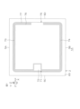
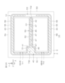
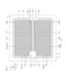
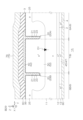
- FIG. 1 is a plan view showing a semiconductor device according to a first embodiment.
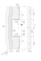
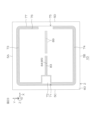
- FIG. 2 is a plan view showing an example layout of a plurality of IGBT regions, boundary regions, gate electrodes, and emitter electrodes.
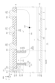
- FIG. 3 is a plan view showing a layout example of the gate wiring, the boundary cathode region, the boundary well region, the outer well region, and the outer cathode region.
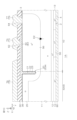
- FIG. 4 is an enlarged plan view showing an example layout of a plurality of IGBT regions and a boundary region.
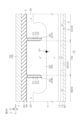
- FIG. 5 is a sectional view taken along the line V-V shown in FIG. 4.
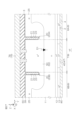
- FIG. 6 is a cross-sectional view taken along line VI-VI shown in FIG. 4.
- FIG. 5 is a sectional view taken along the line V-V shown in FIG. 4.
- FIG. 6 is a cross-sectional view taken along line VI-VI shown in FIG. 4.
- FIG. 5 is a sectional view taken along the line V-V shown in FIG. 4.
- FIG. 7 is a sectional view taken along line VII-VII shown in FIG. 4.
- FIG. 8 is an enlarged plan view showing an example of the layout of the peripheral portion of the IGBT region.
- FIG. 9 is a sectional view taken along line IX-IX shown in FIG. 8.
- FIG. 10 is a cross-sectional view taken along the line XX shown in FIG. 8.
- FIG. 11 is a cross-sectional view showing the peripheral edge of the chip.
- FIG. 12A is a plan view showing another example of the layout of the cathode region.
- FIG. 12B is a plan view showing another example of the layout of the cathode region.
- FIG. 12C is a plan view showing another example of the layout of the cathode region.
- FIG. 12A is a plan view showing another example of the layout of the cathode region.
- FIG. 12B is a plan view showing another example of the layout of the cathode region.
- FIG. 12C is a plan
- FIG. 12D is a plan view showing another example of the layout of the cathode region.
- FIG. 12E is a plan view showing another example of the layout of the cathode region.
- FIG. 12F is a plan view showing another example of the layout of the cathode region.
- FIG. 12G is a plan view showing another example of the layout of the cathode region.
- FIG. 12H is a plan view showing another example of the layout of the cathode region.
- FIG. 12I is a plan view showing another example of the layout of the cathode region.
- FIG. 12J is a plan view showing another example of the layout of the cathode region.
- FIG. 12K is a plan view showing another example of the layout of the cathode region.
- FIG. 12L is a plan view showing another example of the layout of the cathode region.
- FIG. 12M is a plan view showing another example of the layout of the cathode region.
- FIG. 12N is a plan view showing another example of the layout of the cathode region.
- FIG. 13 is a plan view showing the layout of a semiconductor device according to a reference example.
- FIG. 14 is a graph showing the relationship between peak surge current and forward voltage.
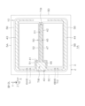
- FIG. 15 is a plan view showing a semiconductor device according to the second embodiment.
- FIG. 16 is a plan view showing an example layout of a plurality of IGBT regions, boundary regions, gate electrodes, and emitter electrodes.
- FIG. 17 is an enlarged plan view showing a layout example of a plurality of IGBT regions and a boundary region.
- FIG. 18 is a sectional view taken along the line XVIII-XVIII shown in FIG. 17.
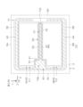
- FIG. 19 is a plan view showing a semiconductor device according to a third embodiment.
- FIG. 20 is a plan view showing an example layout of a plurality of IGBT regions, boundary regions, gate electrodes, and emitter electrodes.
- FIG. 21 is an enlarged plan view showing a layout example of a plurality of IGBT regions and a boundary region.
- FIG. 22 is a sectional view taken along the line XXII-XXII shown in FIG. 21.
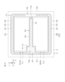
- FIG. 23 is a plan view showing a semiconductor device according to a fourth embodiment.
- FIG. 24 is a plan view showing an example layout of a plurality of IGBT regions, boundary regions, gate electrodes, and emitter electrodes.
- FIG. 25 is an enlarged plan view showing a layout example of a plurality of IGBT regions and a boundary region.
- FIG. 26 is a cross-sectional view showing a main part of the semiconductor device according to the fifth embodiment.
- FIG. 27 is a sectional view showing a main part of a semiconductor device according to a sixth embodiment.
- FIG. 28 is a plan view showing a modification applied to each of the embodiments described above.
- FIG. 29 is a plan view showing a modification applied to each of the embodiments described above.
- FIG. 30 is a plan view showing a modification applied to each of the embodiments described above.
- this phrase includes a numerical value (form) that is equal to the numerical value (form) of the comparison target; It also includes a numerical error (form error) in the range of ⁇ 10% based on (form).
- a numerical value that is equal to the numerical value (form) of the comparison target
- a numerical error form error in the range of ⁇ 10% based on (form).
- words such as “first”, “second”, “third”, etc. are used, but these are symbols attached to the name of each structure to clarify the order of explanation; It is not given for the purpose of limiting the name.
- FIG. 1 is a plan view showing a semiconductor device 1A according to the first embodiment.
- FIG. 2 is a plan view showing an example of the layout of a plurality of IGBT regions 6, boundary regions 7, gate electrodes 71, and emitter electrodes 75.
- FIG. 3 is a plan view showing an example layout of the gate wiring 40, the boundary cathode region 45, the boundary well region 50, the outer cathode region 55, and the outer well region 56.
- FIG. 4 is an enlarged plan view showing a layout example of the plurality of IGBT regions 6 and the boundary region 7. As shown in FIG.
- FIG. 5 is a cross-sectional view taken along the line V-V shown in FIG. 4.
- FIG. 6 is a cross-sectional view taken along line VI-VI shown in FIG. 4.
- FIG. 7 is a sectional view taken along line VII-VII shown in FIG. 4.
- FIG. 8 is an enlarged plan view showing a layout example of the peripheral portion of the IGBT region 6.
- FIG. 9 is a sectional view taken along line IX-IX shown in FIG. 8.
- FIG. 10 is a cross-sectional view taken along the line XX shown in FIG. 8.
- FIG. 11 is a cross-sectional view showing the peripheral portion of the chip 2. As shown in FIG.
- a semiconductor device 1A is an RC-IGBT semiconductor device (semiconductor switching device) having an RC-IGBT (Reverse Conducting - IGBT) integrally equipped with an IGBT (Insulated Gate Bipolar Transistor) and a diode. ).
- the diode is a freewheeling diode for the IGBT.
- the semiconductor device 1A includes a chip 2 having a hexahedral shape (specifically, a rectangular parallelepiped shape).
- Chip 2 may also be referred to as a "semiconductor chip.”
- the chip 2 has a single layer structure made of a silicon single crystal substrate (semiconductor substrate).
- the chip 2 has a first main surface 3 on one side, a second main surface 4 on the other side, and first to fourth side surfaces 5A to 5D connecting the first main surface 3 and the second main surface 4. ing.
- the first main surface 3 and the second main surface 4 are formed into a rectangular shape in a plan view (hereinafter simply referred to as "plan view") when viewed from the normal direction Z thereof.
- the normal direction Z is also the thickness direction of the chip 2.
- the first side face 5A and the second side face 5B extend in a first direction
- the third side surface 5C and the fourth side surface 5D extend in the second direction Y and face the first direction X.
- the semiconductor device 1A includes a plurality of IGBT regions 6 provided at intervals on the chip 2.
- Each IGBT region 6 is a region having an IGBT structure, and may be referred to as an "active region.”
- the multiple IGBT regions 6 include a first IGBT region 6A and a second IGBT region 6B.
- the first IGBT region 6A is provided in a region on the first side surface 5A side with respect to a straight line that crosses the center of the first main surface 3 in the first direction X.
- the second IGBT region 6B is provided in a region on the second side surface 5B side with respect to a straight line that crosses the center of the first main surface 3 in the first direction X.
- the plurality of IGBT regions 6 are each formed in a polygonal shape having four sides parallel to the first to fourth side surfaces 5A to 5D in plan view.
- the semiconductor device 1A includes a boundary region 7 provided in a region between a plurality of IGBT regions 6.
- the boundary region 7 is provided in a band shape extending in the first direction X in the region between the first IGBT region 6A and the second IGBT region 6B.
- the boundary region 7 is located on a straight line that crosses the center of the first main surface 3 in the first direction X.
- the boundary region 7 includes a first region 8 having a relatively large first width in the second direction Y, and a second region 9 having a second width smaller than the first width in the second direction Y.
- the first region 8 is provided on one side (the third side surface 5C side) in the first direction X as a portion that supports the terminal electrode.
- the first region 8 may also be referred to as a "pad region,” "wide region,” or "terminal support region.”
- the first region 8 is located on a straight line that crosses the center of the first main surface 3 in the first direction X in plan view, and is provided in a quadrangular shape near the center of the third side surface 5C.
- the first width of the first region 8 may be 100 ⁇ m or more and 800 ⁇ m or less.
- the first width is preferably 200 ⁇ m or more and 600 ⁇ m or less.
- the first width is set in a range of 350 ⁇ m or more and 450 ⁇ m or less.
- the second region 9 is provided on the other side (the fourth side surface 5D side) of the first region 8 in the first direction X as a portion that supports the wiring.
- the second region 9 is located on a straight line that crosses the center of the first main surface 3 in the first direction X, and is drawn out in a band shape from the first region 8 toward the center of the fourth side surface 5D.
- the second region 9 may be referred to as a "street region,” a "narrow region,” or a "wiring support region.”
- the second width of the second region 9 may be 0.1 ⁇ m or more and 500 ⁇ m or less.
- the second width is preferably 100 ⁇ m or less.
- the second width is 0.1 ⁇ m or more and 0.5 ⁇ m or less, 0.5 ⁇ m or more and 1 ⁇ m or less, 1 ⁇ m or more and 5 ⁇ m or less, 5 ⁇ m or more and 10 ⁇ m or less, 10 ⁇ m or more and 25 ⁇ m or less, 25 ⁇ m or more and 50 ⁇ m or less, 50 ⁇ m or more and 75 ⁇ m or less, and 75 ⁇ m or more. It may be set to a value belonging to any range of 100 ⁇ m or less.
- the semiconductor device 1A includes an outer peripheral region 10 provided at the peripheral edge of the chip 2 so as to collectively surround the plurality of IGBT regions 6.
- the outer peripheral region 10 is provided in an annular shape (square annular shape) extending along the first to fourth side surfaces 5A to 5D.
- the semiconductor device 1A includes an n-type (first conductivity type) drift region 11 formed inside the chip 2.
- Drift region 11 is formed throughout the interior of chip 2 .
- the chip 2 is made of an n-type semiconductor substrate (n-type semiconductor chip), and the drift region 11 is formed using the chip 2.
- the semiconductor device 1A includes an n-type buffer region 12 formed in the surface layer portion of the second main surface 4.
- the buffer region 12 is formed in a layered manner extending along the second main surface 4 over the entire second main surface 4 .
- Buffer region 12 has a higher n-type impurity concentration than drift region 11 .
- the presence or absence of the buffer area 12 is arbitrary, and a configuration without the buffer area 12 may be adopted.
- the semiconductor device 1A includes a p-type (second conductivity type) collector region 13 formed in the surface layer portion of the second main surface 4.
- the collector region 13 is formed in the surface layer portion of the buffer region 12 on the second main surface 4 side.
- the collector region 13 is formed in a layered shape extending along the second main surface 4 over the entire second main surface 4 .
- the collector region 13 is exposed from part of the second main surface 4 and the first to fourth side surfaces 5A to 5D.
- the semiconductor device 1A includes a plurality of trench isolation structures 20 formed on the first main surface 3 to partition a plurality of IGBT regions 6. A gate potential is applied to the plurality of trench isolation structures 20 .
- Trench isolation structure 20 may be referred to as a "trench gate isolation structure” or a "trench gate connection structure.”
- the plurality of trench isolation structures 20 include a first trench isolation structure 20A that defines the first IGBT region 6A, and a second trench isolation structure 20B that defines the second IGBT region 6B.
- the first trench isolation structure 20A surrounds the first IGBT region 6A and partitions the first IGBT region 6A from the boundary region 7 and the outer peripheral region 10.
- the first trench isolation structure 20A is formed into a polygonal ring shape having four sides parallel to the first to fourth side surfaces 5A to 5D in plan view.
- the second trench isolation structure 20B surrounds the second IGBT region 6B and partitions the second IGBT region 6B from the boundary region 7 and the outer peripheral region 10.
- the second trench isolation structure 20B is formed into a polygonal ring shape having four sides parallel to the first to fourth side surfaces 5A to 5D in plan view.
- the plurality of trench isolation structures 20 each have a bent portion so as to partition the first region 8 and the second region 9 of the boundary region 7 in plan view.
- each trench isolation structure 20 has a width less than the width of the second region 9 of the boundary region 7 .
- each trench isolation structure 20 may be 0.5 ⁇ m or more and 5 ⁇ m or less.
- the width of each trench isolation structure 20 is preferably 1 ⁇ m or more and 2.5 ⁇ m or less.
- Each trench isolation structure 20 may have a depth of 1 ⁇ m or more and 20 ⁇ m or less.
- the depth of each trench isolation structure 20 is preferably 4 ⁇ m or more and 10 ⁇ m or less.
- Trench isolation structure 20 includes an isolation trench 21 , an isolation insulating film 22 , and an isolation buried electrode 23 .
- the isolation trench 21 is dug down from the first main surface 3 toward the second main surface 4 and partitions the wall surface of the trench isolation structure 20.
- the isolation insulating film 22 is formed in a film shape along the wall surface of the isolation trench 21 and defines a recess space within the isolation trench 21 .
- the isolation insulating film 22 may include at least one of a silicon oxide film, a silicon nitride film, a silicon oxynitride film, and an aluminum oxide film. It is preferable that the isolation insulating film 22 has a single layer structure consisting of a single insulating film. It is particularly preferable that the isolation insulating film 22 includes a silicon oxide film made of an oxide of the chip 2 .
- the isolation buried electrode 23 is buried in the isolation trench 21 with the isolation insulating film 22 in between.
- the separate buried electrode 23 is made of conductive polysilicon. A gate potential is applied to the separated buried electrode 23.
- the structure on the second IGBT region 6B side is almost the same as the structure on the first IGBT region 6A side. Specifically, the structure on the second IGBT region 6B side is line symmetrical to the structure on the first IGBT region 6A side with respect to the boundary region 7. Below, the structure on the first IGBT region 6A side will be explained. Regarding the description of the structure on the second IGBT region 6B side, the description of the structure on the first IGBT region 6A side is applied and will be omitted.
- the semiconductor device 1A includes a p-type base region 25 formed in the surface layer portion of the first main surface 3 in the first IGBT region 6A.
- Base region 25 may be referred to as a "body region” or a "channel region.”
- the base region 25 is formed at a depth shallower than the trench isolation structure 20 and has a bottom portion located closer to the first main surface 3 than the bottom wall of the trench isolation structure 20 .
- the base region 25 extends in a layered manner along the first main surface 3 and is connected to the inner peripheral wall of the trench isolation structure 20 .
- the semiconductor device 1A includes a plurality of trench structures 30 formed on the first main surface 3 in the first IGBT region 6A.
- a gate potential is applied to the plurality of trench structures 30 .
- Trench structure 30 may be referred to as a "trench gate structure.”
- a plurality of trench structures 30 penetrate base region 25 to reach drift region 11 .
- the plurality of trench structures 30 are arranged at intervals in the first direction X in a plan view, and are each formed in a band shape extending in the second direction Y. That is, the plurality of trench structures 30 are arranged in stripes extending in the second direction Y.
- the plurality of trench structures 30 each have a first end 30A on the boundary region 7 side and a second end 30B on the outer peripheral region 10 side in the longitudinal direction (second direction Y).
- the first end 30A and the second end 30B are mechanically and electrically connected to the trench isolation structure 20.
- the plurality of trench structures 30 together with the trench isolation structure 20 constitute one ladder-like trench gate structure.
- the connection between trench structure 30 and trench isolation structure 20 may be considered as part of trench isolation structure 20 or may be considered as part of trench structure 30.
- the plurality of trench structures 30 may be arranged in the first direction X at intervals of 0.5 ⁇ m or more and 5 ⁇ m or less.
- the interval between the plurality of trench structures 30 is preferably 1 ⁇ m or more and 3 ⁇ m or less.
- the spacing between the plurality of trench structures 30 is less than the width of the second region 9 of the boundary region 7 .
- Each trench structure 30 may have a width of 0.5 ⁇ m or more and 5 ⁇ m or less.
- the width of each trench structure 30 is the width in a direction perpendicular to the direction in which each trench structure 30 extends.
- the width of each trench structure 30 is preferably 1 ⁇ m or more and 2.5 ⁇ m or less.
- the width of each trench structure 30 is less than the width of the second region 9 of the boundary region 7.
- the width of each trench structure 30 is approximately equal to the width of trench isolation structure 20.
- Each trench structure 30 may have a depth of 1 ⁇ m or more and 20 ⁇ m or less.
- the depth of each trench structure 30 is preferably 4 ⁇ m or more and 10 ⁇ m or less.
- the depth of each trench structure 30 is approximately equal to the depth of trench isolation structure 20.
- Trench structure 30 includes a gate trench 31, a gate insulating film 32, and a gate buried electrode 33.
- the gate trench 31 is dug down from the first main surface 3 toward the second main surface 4 and partitions the wall surface of the trench structure 30.
- the gate trench 31 communicates with the isolation trench 21 at both ends (first end 30A and second end 30B) in the second direction Y.
- the side wall of the gate trench 31 communicates with the side wall of the isolation trench 21, and the bottom wall of the gate trench 31 communicates with the bottom wall of the isolation trench 21.
- the gate insulating film 32 is formed in a film shape along the wall surface of the gate trench 31, and defines a recess space within the gate trench 31.
- the gate insulating film 32 may include at least one of a silicon oxide film, a silicon nitride film, a silicon oxynitride film, and an aluminum oxide film.
- the gate insulating film 32 has a single layer structure consisting of a single insulating film. It is particularly preferable that the gate insulating film 32 includes a silicon oxide film made of the oxide of the chip 2. In this embodiment, the gate insulating film 32 is made of the same insulating film as the isolation insulating film 22. Gate insulating film 32 is connected to isolation insulating film 22 at a communication portion between isolation trench 21 and gate trench 31 .
- the gate buried electrode 33 is buried in the gate trench 31 with the gate insulating film 32 in between.
- the gate buried electrode 33 is made of conductive polysilicon.
- a gate potential is applied to the gate buried electrode 33.
- the gate buried electrode 33 is connected to the separated buried electrode 23 at a communication portion between the separated trench 21 and the gate trench 31 .
- the semiconductor device 1A includes a plurality of n-type emitter regions 35 formed in the surface layer of the base region 25.
- the plurality of emitter regions 35 are arranged on both sides of the plurality of trench structures 30 and are each formed in a band shape extending along the plurality of trench structures 30 in plan view.
- Each of the plurality of emitter regions 35 has a higher n-type impurity concentration than the drift region 11.
- the semiconductor device 1A includes a plurality of n-type carrier storage regions 36 formed in a region immediately below the base region 25 within the chip 2.
- the plurality of carrier storage regions 36 suppress the discharge of carriers (holes) to the base region 25 and promote accumulation of carriers (holes) in the region directly under the plurality of trench structures 30 .
- the plurality of carrier storage regions 36 promotes lower on-resistance and lower on-voltage from the inside of the chip 2.
- the plurality of carrier storage regions 36 are arranged on both sides of the plurality of trench structures 30 and are each formed in a band shape extending along the plurality of trench structures 30 in plan view.
- a plurality of carrier storage regions 36 are each formed in a region between the bottom of the base region 25 and the bottom wall of the trench structure 30 in the thickness direction of the chip 2.
- the plurality of carrier storage regions 36 are spaced apart from the bottom wall of the trench structure 30 toward the base region 25 .
- the bottoms of the plurality of carrier storage regions 36 are preferably located closer to the bottom wall of the trench structure 30 than the middle part of the trench structure 30.
- the plurality of carrier storage regions 36 have a higher n-type impurity concentration than the drift region 11.
- the n-type impurity concentration of the plurality of carrier storage regions 36 is preferably lower than that of the emitter region 35.
- the presence or absence of the carrier storage area 36 is optional. Therefore, a configuration without the carrier storage area 36 may be adopted.
- the semiconductor device 1A includes a plurality of contact holes 37 formed in the first main surface 3 so as to expose the emitter region 35.
- the plurality of contact holes 37 are formed on both sides of the plurality of trench structures 30 at intervals in the first direction X from the plurality of trench structures 30 .
- the plurality of contact holes 37 may each be formed in a tapered shape in which the opening width narrows from the opening toward the bottom wall.
- the plurality of contact holes 37 may be spaced apart from the bottom of the emitter region 35 toward the first main surface 3 so as not to reach the base region 25. Of course, the plurality of contact holes 37 may extend through the emitter region 35 to reach the base region 25.
- the plurality of contact holes 37 are each formed in a band shape extending along the plurality of trench structures 30 in plan view. The plurality of contact holes 37 are shorter than the plurality of trench structures 30 in the longitudinal direction (second direction Y).
- the semiconductor device 1A includes a plurality of p-type contact regions 38 formed in a region different from the plurality of emitter regions 35 in the surface layer portion of the base region 25.
- the plurality of contact regions 38 are each formed in a band shape extending along the corresponding contact hole 37 in plan view.
- the bottoms of the plurality of contact regions 38 are each formed in a region between the bottom wall of the corresponding contact hole 37 and the bottom of the base region 25 .
- the plurality of contact regions 38 have a higher p-type impurity concentration than the base region 25.
- the first IGBT region 6A includes a base region 25, a plurality of trench structures 30, a plurality of emitter regions 35, a plurality of carrier storage regions 36, a plurality of contact holes 37, and a plurality of contact regions 38.
- the second IGBT region 6B like the first IGBT region 6A, includes a base region 25, a plurality of trench structures 30, a plurality of emitter regions 35, a plurality of carrier storage regions 36, a plurality of contact holes 37, and a plurality of contact regions 38. .
- the semiconductor device 1A includes a main surface insulating film 39 that covers the first main surface 3.
- Main surface insulating film 39 may include at least one of a silicon oxide film, a silicon nitride film, a silicon oxynitride film, and an aluminum oxide film. It is preferable that the main surface insulating film 39 has a single layer structure consisting of a single insulating film. It is particularly preferable that the main surface insulating film 39 includes a silicon oxide film made of an oxide of the chip 2 . In this embodiment, the main surface insulating film 39 is made of the same insulating film as the gate insulating film 32.
- the main surface insulating film 39 extends like a film along the first main surface 3 so as to cover the plurality of IGBT regions 6 , the boundary region 7 , and the outer peripheral region 10 .
- the main surface insulating film 39 may be continuous with the periphery of the chip 2 (first to fourth side surfaces 5A to 5D).
- the main surface insulating film 39 covers the first main surface 3 so as to expose the plurality of trench isolation structures 20 and the plurality of trench structures 30.
- main surface insulating film 39 is connected to isolation insulating film 22 and gate insulating film 32, and exposes isolation buried electrode 23 and gate buried electrode 33.
- the semiconductor device 1A includes a gate wiring 40 arranged anywhere above the first main surface 3. Specifically, the gate wiring 40 is arranged in a film shape anywhere on the main surface insulating film 39. In this form, the gate wiring 40 is made of a conductive polysilicon film. The gate wiring 40 is routed at least in the boundary region 7. In this embodiment, the gate wiring 40 is routed in the boundary region 7 and the outer peripheral region 10 in an arbitrary layout.
- the gate wiring 40 includes a pad wiring 41, a boundary wiring 42, a first outer wiring 43, and a second outer wiring 44.
- the pad wiring 41 is arranged on the first region 8 of the boundary region 7 and has a relatively large first wiring width in the second direction Y.
- the pad wiring 41 is formed into a rectangular shape in plan view.
- the pad wiring 41 has a width in the second direction Y that is larger than the width of the boundary region 7 (the first width of the first region 8).
- the pad wiring 41 is drawn out from above the boundary region 7 onto a plurality of trench isolation structures 20 adjacent to each other in the second direction Y.
- the pad wiring 41 is drawn out from above the boundary region 7 to above the plurality of IGBT regions 6 so as to cover the first ends 30A of the plurality of trench structures 30. Thereby, the pad wiring 41 is mechanically and electrically connected to the separated buried electrode 23 and the plurality of gate buried electrodes 33, and transmits the gate potential to the separated buried electrode 23 and the gate buried electrode 33.
- the pad wiring 41 is formed integrally with the separate buried electrode 23 and the plurality of gate buried electrodes 33.
- the boundary wiring 42 is drawn out from the pad wiring 41 onto the second region 9 of the boundary region 7, and has a second wiring width smaller than the first wiring width of the pad wiring 41 in the second direction Y.
- the boundary wiring 42 is formed in a band shape extending in the first direction X. In this form, the boundary wiring 42 crosses the center of the chip 2.
- the boundary wiring 42 has a width in the second direction Y that is larger than the width of the boundary region 7 (the second width of the second region 9).
- the boundary wiring 42 is drawn out from above the boundary region 7 onto a plurality of trench isolation structures 20 adjacent to each other in the second direction Y.
- the boundary wiring 42 is drawn out from above the boundary region 7 to above the plurality of IGBT regions 6 so as to cover the first ends 30A of the plurality of trench structures 30. Thereby, the boundary wiring 42 is mechanically and electrically connected to the separated buried electrode 23 and the plurality of gate buried electrodes 33, and transmits the gate potential to the separated buried electrode 23 and the gate buried electrodes 33. In this form, the boundary wiring 42 is formed integrally with the separated buried electrode 23 and the plurality of gate buried electrodes 33.
- the first outer wiring 43 is drawn out from the pad wiring 41 onto the outer peripheral region 10 and is formed in a band shape extending along the first side surface 5A and the third side surface 5C.
- the first outer wiring 43 may have a portion extending in a band shape along the fourth side surface 5D.
- the first outer wiring 43 has a portion extending along the first side surface 5A and drawn out from above the outer peripheral region 10 onto the first trench isolation structure 20A. In this form, the first outer wiring 43 also covers the second ends 30B of the plurality of trench structures 30 in the first IGBT region 6A.
- the first outer wiring 43 is mechanically and electrically connected to the separated buried electrode 23 and the plurality of gate buried electrodes 33.
- the first outer wiring 43 is formed integrally with the separate buried electrode 23 and the plurality of gate buried electrodes 33.
- the first outer wiring 43 transmits the gate potential from the outer peripheral region 10 side to the separated buried electrode 23 and the gate buried electrode 33.
- the second outer wiring 44 is drawn out from the pad wiring 41 onto the outer peripheral region 10 and is formed in a band shape extending along the second side surface 5B and the third side surface 5C.
- the second outer wiring 44 may have a portion extending in a band shape along the fourth side surface 5D.
- the second outer wiring 44 has a portion extending along the second side surface 5B and drawn out from above the outer peripheral region 10 onto the second trench isolation structure 20B. In this form, the second outer wiring 44 also covers the second ends 30B of the plurality of trench structures 30 in the second IGBT region 6B.
- the second outer wiring 44 is mechanically and electrically connected to the separated buried electrode 23 and the plurality of gate buried electrodes 33.
- the second outer wiring 44 is formed integrally with the separate buried electrode 23 and the plurality of gate buried electrodes 33.
- the second outer wiring 44 transmits the gate potential from the outer peripheral region 10 side to the separated buried electrode 23 and the gate buried electrode 33.
- semiconductor device 1A includes an n-type boundary cathode region 45 formed in the surface layer of second main surface 4 in boundary region 7.
- the boundary cathode region 45 is formed in a layered manner extending along the second main surface 4 .
- Boundary cathode region 45 passes through collector region 13 so as to be connected to buffer region 12 and is exposed from second main surface 4 .
- the boundary cathode region 45 has an n-type impurity concentration higher than the p-type impurity concentration of the collector region 13, and consists of a region in which the conductivity type of a part of the collector region 13 is replaced from the p-type to the n-type.
- the boundary cathode region 45 preferably has a higher n-type impurity concentration than the drift region 11 (buffer region 12).
- the boundary cathode region 45 is formed in a region sandwiched between the first trench isolation structure 20A and the second trench isolation structure 20B in plan view. That is, the boundary cathode region 45 is formed in a region sandwiched between the plurality of trench structures 30 on the first IGBT region 6A side and the plurality of trench structures 30 on the second IGBT region 6B side in plan view.
- the boundary cathode region 45 connects the base region 25 of each IGBT region 6 in the direction along the second main surface 4 (second direction Y) so as not to face the base region 25 of each IGBT region 6 in the thickness direction of the chip 2. It is preferable that they are formed with a space between them.
- the boundary cathode region 45 is formed at a distance from the plurality of trench structures 30 in the direction along the second main surface 4 (second direction Y) so as not to face the plurality of trench structures 30 in the thickness direction of the chip 2. It is particularly preferable that the In this form, the boundary cathode region 45 is formed by forming a plurality of trench isolation structures 20 in the direction along the second main surface 4 (second direction Y) so as not to face the plurality of trench isolation structures 20 in the thickness direction of the chip 2. They are formed at intervals from.
- the boundary cathode region 45 has a width smaller than the width of the boundary region 7 in the second direction Y. Further, the boundary cathode region 45 is formed only in the boundary region 7 and not in the plurality of IGBT regions 6. Further, the boundary cathode region 45 is formed in the surface layer portion of the second main surface 4 so that a part of the collector region 13 remains within the boundary region 7 . That is, the semiconductor device 1A includes the collector region 13 formed in the boundary region 7.
- the boundary cathode region 45 has a width smaller than the width of the gate wiring 40 (boundary wiring 42) in the second direction Y in plan view, and has a peripheral edge located inward from the peripheral edge of the gate wiring 40. It has a department. That is, in cross-sectional view, the entire boundary cathode region 45 faces the gate wiring 40 in the thickness direction of the chip 2.
- the boundary cathode region 45 may have a width larger than the width of the gate wiring 40 in a plan view, and a peripheral edge located outside the peripheral edge of the gate wiring 40.
- the boundary cathode region 45 is formed in a band shape extending along the boundary region 7 in plan view. In other words, the boundary cathode region 45 extends along the direction in which the plurality of trench structures 30 are arranged.
- the boundary cathode region 45 faces the gate wiring 40 in the thickness direction of the chip 2. Specifically, the boundary cathode region 45 faces the pad wiring 41 and the boundary wiring 42 in the thickness direction of the chip 2.
- the boundary cathode region 45 includes a first cathode region 46 formed in the first region 8 of the boundary region 7 and a second cathode region 47 formed in the second region 9 of the boundary region 7. include.
- the first cathode region 46 has a relatively large first cathode width in the second direction Y, and faces the pad wiring 41 in the thickness direction of the chip 2.
- the first cathode region 46 is formed into a rectangular shape in plan view.
- the first cathode region 46 has a first cathode width that is less than or equal to the first wiring width of the pad wiring 41 (more preferably less than the first wiring width).
- the first cathode region 46 has a first cathode width that is less than or equal to the first width (specifically, less than the first width) of the first region 8 of the boundary region 7 . That is, the first cathode region 46 has a planar area that is less than or equal to the planar area of the first region 8 (specifically, less than the planar area of the first region 8).
- the first cathode region 46 preferably has a first cathode width that is 1/10 or more of the first width.
- the second cathode region 47 has a second cathode width smaller than the first cathode width of the first cathode region 46 in the second direction Y, and extends from the first cathode region 46 toward the second region 9 of the boundary region 7. It is pulled out in a strip.
- the second cathode region 47 faces the boundary wiring 42 in the thickness direction of the chip 2.
- the second cathode region 47 is located on a straight line that crosses the center of the first main surface 3 in the first direction X.
- the second cathode region 47 includes a region on one side (third side surface 5C side) in the first direction X with respect to a straight line crossing the center of the first main surface 3 in the second direction Y, and a region on the other side ( 4th side surface 5D side) and extends in a band shape.
- the second cathode region 47 has a second cathode width that is less than or equal to the second wiring width of the boundary wiring 42 (more preferably less than the second wiring width).
- the second cathode region 47 has a second cathode width that is less than or equal to the second width (specifically less than the second width) of the second region 9 of the boundary region 7 . That is, the second cathode region 47 has a planar area that is less than or equal to the planar area of the second region 9 (specifically, less than the planar area of the second region 9).
- the second cathode region 47 preferably has a second cathode width that is 1/10 or more of the second width.
- the semiconductor device 1A includes a p-type boundary well region 50 formed in the surface layer of the first main surface 3 in the boundary region 7.
- Boundary well region 50 may be referred to as a "boundary anode region.”
- boundary well region 50 has a higher p-type impurity concentration than base regions 25 .
- the boundary well region 50 may have a lower p-type impurity concentration than the plurality of base regions 25.
- the boundary well region 50 is formed in a layer shape extending along the first main surface 3 and is exposed from the first main surface 3.
- Boundary well region 50 is formed in a region sandwiched between first trench isolation structure 20A and second trench isolation structure 20B. That is, the boundary well region 50 is formed in a region sandwiched between the plurality of trench structures 30 on the first IGBT region 6A side and the plurality of trench structures 30 on the second IGBT region 6B side.
- the boundary well region 50 is formed deeper than the plurality of base regions 25 and is connected to the plurality of trench isolation structures 20. Specifically, the boundary well region 50 is formed deeper than the plurality of trench isolation structures 20 (the plurality of trench structures 30) and has a portion that covers the bottom walls of the plurality of trench isolation structures 20.
- the boundary well region 50 has a width greater than the width of the boundary region 7 in the second direction Y, and is drawn out from the boundary region 7 into each IGBT region 6.
- the boundary well region 50 has a width larger than the width of the gate wiring 40 in the second direction Y, and has a peripheral edge that extends outward from the peripheral edge of the gate wiring 40 (toward the inner side of each IGBT region 6). It is preferable to have the following.
- Boundary well region 50 has a portion that traverses trench isolation structures 20 and covers the bottom walls of trench structures 30 .
- the boundary well region 50 covers the sidewalls of the trench isolation structure 20 and the sidewalls of the plurality of trench structures 30 in each IGBT region 6 and is connected to each base region 25 in the surface layer portion of the first main surface 3. Boundary well region 50 is electrically connected to base region 25 and emitter region 35 within each IGBT region 6 .
- the depth of the boundary well region 50 may be greater than or equal to 1 ⁇ m and less than or equal to 20 ⁇ m.
- the depth of the boundary well region 50 is preferably 5 ⁇ m or more and 10 ⁇ m or less.
- the boundary well region 50 faces the boundary cathode region 45 in the thickness direction of the chip 2. Specifically, the boundary well region 50 has a width greater than the width of the boundary cathode region 45 in the second direction Y, and has a portion (inner portion) facing the boundary cathode region 45 in the thickness direction of the chip 2. , and a portion (periphery) facing the collector region 13 in the thickness direction of the chip 2 .
- the boundary well region 50 faces the collector region 13 and the boundary cathode region 45 in a portion located within the boundary region 7 , and faces the collector region 13 in a portion located within each IGBT region 6 . That is, the boundary well region 50 has a portion facing the collector region 13 in each IGBT region 6 and the boundary region 7.
- the boundary well region 50 preferably faces the entire boundary cathode region 45 in cross-sectional view.
- the boundary well region 50 is formed in a band shape extending along the boundary region 7 in plan view. In other words, the boundary well region 50 extends along the direction in which the plurality of trench structures 30 are arranged.
- the boundary well region 50 faces the gate wiring 40 and the boundary cathode region 45 in the thickness direction of the chip 2. Specifically, the boundary well region 50 faces the pad wiring 41 and the boundary wiring 42 in the thickness direction of the chip 2, and faces the first cathode region 46 and the second cathode region 47 in the thickness direction of the chip 2. ing.
- the boundary well region 50 includes a first well region 51 formed in the first region 8 of the boundary region 7 and a second well region 52 formed in the second region 9 of the boundary region 7. include.
- the first well region 51 has a relatively large first well width in the second direction Y, and faces the pad wiring 41 and the first cathode region 46 in the thickness direction of the chip 2.
- the first well region 51 is formed into a rectangular shape in plan view.
- the first well region 51 has a first well width that is equal to or larger than the first cathode width of the first cathode region 46 (more preferably larger than the first cathode width).
- the first well region 51 preferably faces the entire first cathode region 46 in the thickness direction of the chip 2 in a cross-sectional view. It is particularly preferable that the first well region 51 has a planar area larger than or equal to the planar area of the first cathode region 46 (more preferably larger than the planar area of the first cathode region 46).
- the first well region 51 preferably has a first well width that is greater than or equal to the first wiring width of the pad wiring 41 (more preferably a first well width that is larger than the first wiring width).
- the first well region 51 preferably faces the entire area of the pad wiring 41 in the thickness direction of the chip 2 in a cross-sectional view. It is particularly preferable that the first well region 51 has a planar area larger than or equal to the planar area of the pad wiring 41 (more preferably larger than the planar area of the pad wiring 41).
- the first well region 51 has a first well width that is equal to or larger than the first width of the first region 8 of the boundary region 7 (more preferably larger than the first width). It is particularly preferable that the first well region 51 has a planar area equal to or larger than the planar area of the first region 8 (more preferably larger than the planar area of the first region 8).
- the first well width is preferably at most twice the first width (more preferably at most 1.5 times the first width).
- the second well region 52 is drawn out in a strip shape from the first well region 51 toward the second region 9 of the boundary region 7, and has a second well region smaller than the first well width of the first well region 51 in the second direction Y. It has a width.
- the second well region 52 faces the boundary wiring 42 and the second cathode region 47 in the thickness direction of the chip 2.
- the second well region 52 is located on a straight line that crosses the center of the first main surface 3 in the first direction X.
- the second well region 52 includes a region on one side (the third side surface 5C side) in the first direction 4th side surface 5D side) and extends in a band shape.
- the second well region 52 has a second well width that is equal to or larger than the second cathode width of the second cathode region 47 (more preferably larger than the second cathode width).
- the second well region 52 preferably faces the entire second cathode region 47 in the thickness direction of the chip 2 in a cross-sectional view. It is particularly preferable that the second well region 52 has a planar area that is greater than or equal to the planar area of the second cathode region 47 (more preferably larger than the planar area of the second cathode region 47).
- the second well region 52 has a second well width that is equal to or larger than the second wiring width of the boundary wiring 42 (more preferably larger than the second wiring width).
- the second well region 52 preferably faces the entire boundary wiring 42 in the thickness direction of the chip 2 in a cross-sectional view. It is particularly preferable that the second well region 52 has a planar area equal to or larger than the planar area of the boundary wiring 42 (more preferably larger than the planar area of the boundary wiring 42).
- the second well region 52 has a second well width that is equal to or larger than the second width of the second region 9 of the boundary region 7 (more preferably larger than the second width). It is particularly preferable that the second well region 52 has a planar area equal to or larger than the planar area of the second region 9 (more preferably larger than the planar area of the second region 9).
- the second well width is preferably at most twice the second width (more preferably at most 1.5 times the second width).
- the semiconductor device 1A includes an n-type outer cathode region 55 formed in the surface layer portion of the second main surface 4 in the outer peripheral region 10.
- the outer cathode region 55 is formed in a layered shape extending along the second main surface 4 .
- the outer cathode region 55 passes through the collector region 13 so as to be connected to the buffer region 12 and is exposed from the second main surface 4 .
- the outer cathode region 55 has an n-type impurity concentration higher than the p-type impurity concentration of the collector region 13, and is a region in which the conductivity type of a part of the collector region 13 is replaced from the p-type to the n-type. It is preferable that the outer cathode region 55 has a higher n-type impurity concentration than the drift region 11 (buffer region 12).
- the n-type impurity concentration of outer cathode region 55 is preferably approximately equal to the n-type impurity concentration of boundary cathode region 45 .
- the outer cathode region 55 is formed spaced inward from the periphery of the second main surface 4 (first to fourth side surfaces 5A to 5D).
- the outer cathode region 55 is formed in a band shape extending along the plurality of IGBT regions 6 in plan view.
- the outer cathode region 55 is formed in an annular shape surrounding the plurality of IGBT regions 6 in plan view.
- the outer cathode region 55 is formed in an annular shape (quadrangular annular shape) having four sides parallel to the periphery of the second main surface 4 .
- the outer cathode region 55 is formed at intervals from the base region 25 of each IGBT region 6 toward the periphery of the chip 2 so as not to face the base region 25 of each IGBT region 6 at least in the thickness direction of the chip 2.
- the outer cathode region 55 is formed at intervals from the plurality of trench structures 30 toward the periphery of the chip 2 so as not to face the plurality of trench structures 30 in the thickness direction of the chip 2.
- the outer cathode region 55 is formed at a distance from the plurality of trench isolation structures 20 toward the periphery of the chip 2 so as not to face the plurality of trench isolation structures 20 in the thickness direction of the chip 2. . That is, it is preferable that the outer cathode region 55 be formed only in the outer peripheral region 10 and not in the plurality of IGBT regions 6.
- the outer cathode region 55 may be connected to the boundary cathode region 45 at the connection portion between the boundary region 7 and the outer peripheral region 10.
- the outer cathode region 55 faces the first outer wiring 43 and the second outer wiring 44 of the gate wiring 40 in the thickness direction of the chip 2 .
- the ratio of the planar area of the cathode region to the planar area of the second main surface 4 is preferably 0.1% or more and 10% or less.
- the planar area of the cathode region is the total planar area of the border cathode region 45 and the outer cathode region 55.
- the proportion of the planar area of the cathode region is 0.1% or more and 1% or less, 1% or more and 2% or less, 2% or more and 4% or less, 4% or more and 6% or less, 6% or more and 8% or less, and 8%. It may belong to any one range of 10% or more.
- the semiconductor device 1A includes a p-type outer well region 56 formed in the surface layer of the first main surface 3 in the outer peripheral region 10.
- the outer well region 56 may be referred to as the "outer anode region.”
- outer well region 56 has a higher p-type impurity concentration than base regions 25 .
- the boundary well region 50 may have a lower p-type impurity concentration than the plurality of base regions 25.
- the p-type impurity concentration of the outer well region 56 is approximately equal to the p-type impurity concentration of the boundary well region 50.
- the outer well region 56 is formed in a layer shape extending along the first main surface 3 and is exposed from the first main surface 3.
- the outer well region 56 is formed at a distance inward from the periphery of the first main surface 3 (first to fourth side surfaces 5A to 5D).
- the outer well region 56 is formed in a band shape extending along the plurality of IGBT regions 6 in plan view.
- the outer well region 56 is formed in an annular shape surrounding the plurality of IGBT regions 6 in plan view.
- the outer well region 56 is formed in an annular shape (quadrangular annular shape) having four sides parallel to the periphery of the first main surface 3 .
- the outer well region 56 is formed deeper than the plurality of base regions 25. Specifically, the outer well region 56 is formed deeper than the plurality of trench isolation structures 20 (the plurality of trench structures 30). Outer well region 56 has approximately the same depth as border well region 50 in this configuration.
- the outer well region 56 is connected to the plurality of trench isolation structures 20.
- the outer well region 56 has a portion that covers the bottom walls of the plurality of trench isolation structures 20 .
- the outer well region 56 is drawn out from the outer peripheral region 10 into each IGBT region 6 .
- the outer well region 56 has a portion that traverses the plurality of trench isolation structures 20 and covers the bottom walls of the plurality of trench structures 30.
- the outer well region 56 covers the sidewalls of the trench isolation structure 20 and the plurality of trench structures 30 in each IGBT region 6, and is connected to the plurality of base regions 25 in the surface layer portion of the first main surface 3. Outer well region 56 is electrically connected to base region 25 and emitter region 35 within each IGBT region 6 .
- the outer well region 56 faces the outer cathode region 55 in the thickness direction of the chip 2.
- the outer well region 56 has a width larger than the width of the outer cathode region 55 and has a portion (inner portion) facing the outer cathode region 55 in the thickness direction of the chip 2, and a portion (inner portion) that is larger than the width of the outer cathode region 55. It has a portion (periphery) that faces the collector region 13 in the thickness direction. More specifically, the outer well region 56 has an inner edge on the inner side of the first main surface 3 and an outer edge on the peripheral edge side of the first main surface 3. The inner edge and outer edge of the outer well region 56 face the collector region 13 in the thickness direction of the chip 2.
- the outer well region 56 faces the collector region 13 and the outer cathode region 55 in a portion located within the outer peripheral region 10 (inner portion and outer edge portion), and a portion located within each IGBT region 6 (inner edge portion). portion) facing the collector region 13. That is, the outer well region 56 has a portion facing the collector region 13 in each IGBT region 6 and the outer peripheral region 10 .
- Border well region 50 preferably faces the entire border cathode region 45 .
- the outer well region 56 is connected to the boundary well region 50 at the junction between the boundary region 7 and the outer peripheral region 10.
- the outer cathode region 55 faces the first outer wiring 43 and the second outer wiring 44 of the gate wiring 40 in the thickness direction of the chip 2 .
- the semiconductor device 1A includes at least one (in this embodiment, a plurality of) p-type field regions 57 formed in the surface layer portion of the first main surface 3 in the outer peripheral region 10.
- the number of field regions 57 is arbitrary, and may be 1 or more and 20 or less (typically 3 or more and 10 or less).
- the plurality of field regions 57 may have a higher p-type impurity concentration than the plurality of base regions 25.
- the plurality of field regions 57 may have a higher p-type impurity concentration than the outer well region 56.
- the plurality of field regions 57 may have approximately the same p-type impurity concentration as the outer well region 56.
- the plurality of field regions 57 are formed in an electrically floating state.
- the plurality of field regions 57 are formed in a region between the periphery of the first main surface 3 and the outer well region 56 at intervals from the periphery of the first main surface 3 and the outer well region 56 . That is, the plurality of field regions 57 are formed at positions that do not face the outer cathode region 55 in the thickness direction of the chip 2.
- the plurality of field regions 57 are formed in a band shape extending along the outer well region 56 in plan view. In this embodiment, the plurality of field regions 57 are formed in an annular shape (quadrangular annular shape) surrounding the outer well region 56 in plan view.
- the plurality of field regions 57 are formed deeper than the plurality of base regions 25.
- the plurality of field regions 57 are formed with a constant depth.
- the plurality of field regions 57 are arranged such that the interval between the plurality of field regions 57 gradually increases toward the peripheral edge of the first main surface 3.
- each of the plurality of field regions 57 has a width smaller than the width of the outer well region 56. It is preferable that the outermost field region 57 among the plurality of field regions 57 is formed wider than the other field regions 57 .
- the width of each field region 57 may be 1 ⁇ m or more and 50 ⁇ m or less.
- the width of each field area 57 is 1 ⁇ m or more and 2.5 ⁇ m or less, 2.5 ⁇ m or more and 5 ⁇ m or less, 5 ⁇ m or more and 7.5 ⁇ m or less, 7.5 ⁇ m or more and 10 ⁇ m or less, 10 ⁇ m or more and 20 ⁇ m or less, 20 ⁇ m or more and 30 ⁇ m or less, and 30 ⁇ m or more and 40 ⁇ m or less. , and may be set to a value belonging to any one of the ranges of 40 ⁇ m or more and 50 ⁇ m or less.
- the width of each field region 57 is preferably 10 ⁇ m or more and 30 ⁇ m or less.
- the semiconductor device 1A includes an n-type channel stop region 58 formed in the surface layer of the first main surface 3 at intervals from the plurality of field regions 57 to the peripheral edge side of the first main surface 3 in the outer peripheral region 10.
- Channel stop region 58 has a higher n-type impurity concentration than drift region 11.
- the channel stop region 58 may be exposed from the first to fourth side surfaces 5A to 5D.
- the channel stop region 58 is formed in a band shape extending along the periphery of the first main surface 3 in plan view.
- the channel stop region 58 is formed in an annular shape (quadrangular annular shape) surrounding the plurality of field regions 57 in plan view.
- Channel stop region 58 is formed in an electrically floating state.
- the semiconductor device 1A includes an interlayer insulating film 60 that covers the main surface insulating film 39.
- Interlayer insulating film 60 may include at least one of a silicon oxide film, a silicon nitride film, a silicon oxynitride film, and an aluminum oxide film.
- the interlayer insulating film 60 may include at least one of a NSG (Non-doped Silicate Glass) film, a PSG (Phosphor Silicate Glass) film, and a BPSG (Boron Phosphor Silicate Glass) film as an example of a silicon oxide film. good.
- the interlayer insulating film 60 may have a single layer structure consisting of a single insulating film or a laminated structure including a plurality of insulating films.
- the interlayer insulating film 60 has a thickness that exceeds the thickness of the main surface insulating film 39.
- the interlayer insulating film 60 may extend in a layered manner along the first main surface 3 and may be continuous with the periphery of the chip 2 (first to fourth side surfaces 5A to 5D).
- the interlayer insulating film 60 selectively covers the plurality of IGBT regions 6 , the boundary region 7 , and the outer peripheral region 10 .
- the interlayer insulating film 60 covers the main surface insulating film 39, the plurality of trench isolation structures 20, and the plurality of trench structures 30 in each IGBT region 6.
- Interlayer insulating film 60 covers main surface insulating film 39 and gate wiring 40 in boundary region 7 and outer peripheral region 10 .
- the interlayer insulating film 60 has a plurality of contact openings 61 that expose the plurality of emitter regions 35 in each IGBT region 6.
- the plurality of contact openings 61 are formed in a one-to-one correspondence with the plurality of contact holes 37, and communicate with the corresponding contact holes 37, respectively.
- the plurality of contact openings 61 are each formed in a band shape extending along the corresponding contact hole 37 in plan view.
- the interlayer insulating film 60 includes at least one (in this form, a plurality of) gate openings 62 that selectively expose the gate wiring 40 in the boundary region 7 and the outer peripheral region 10.
- the plurality of gate openings 62 include at least one gate opening 62 that selectively exposes the pad wiring 41 , at least one gate opening 62 that selectively exposes the first outer wiring 43 , and a selected second outer wiring 44 .
- the gate opening 62 may include at least one gate opening 62 that exposes the gate.
- the interlayer insulating film 60 includes at least one (in this form, a plurality of) first well openings 63 that selectively expose the inner edge of the outer well region 56 in the outer peripheral region 10. Specifically, the plurality of first well openings 63 expose the inner edge of the outer well region 56 in the region between the plurality of trench isolation structures 20 and the gate wiring 40.
- the interlayer insulating film 60 includes at least one (one in this form) second well opening 64 that selectively exposes the outer edge of the outer well region 56 in the outer peripheral region 10 .
- the second well opening 64 exposes the outer edge of the outer well region 56 in a region closer to the peripheral edge of the first main surface 3 than the gate wiring 40 .
- the second well opening 64 is formed in a band shape extending along the plurality of IGBT regions 6.
- the second well opening 64 is formed in an annular shape (quadrangular annular shape) surrounding the plurality of IGBT regions 6 .
- the interlayer insulating film 60 includes at least one (plurality in this embodiment) field opening 65 that selectively exposes at least one (plurality in this embodiment) field region 57 in the outer peripheral region 10 .
- the plurality of field openings 65 expose the plurality of field regions 57 in a one-to-one correspondence.
- the plurality of field openings 65 are formed in a band shape extending along the plurality of field regions 57.
- the plurality of field openings 65 are formed in an annular shape (quadrangular annular shape) extending along the plurality of field regions 57.
- the interlayer insulating film 60 includes a channel stop opening 66 that exposes the channel stop region 58 in the outer peripheral region 10.
- Channel stop opening 66 is formed in a band shape extending along channel stop region 58 .
- the channel stop opening 66 is formed in an annular shape (quadrangular annular shape) extending along the channel stop region 58 and communicates with the periphery of the first main surface 3 .
- the semiconductor device 1A includes a plurality of via electrodes 70 embedded in an interlayer insulating film 60 so as to be electrically connected to a plurality of emitter regions 35.
- the plurality of via electrodes 70 are embedded in the plurality of contact openings 61 in the interlayer insulating film 60.
- the plurality of via electrodes 70 include a portion in contact with the chip 2 and a portion in contact with the interlayer insulating film 60.
- the plurality of via electrodes 70 are electrically connected to the emitter region 35 and the contact region 38 at the portions in contact with the chip 2 .
- Each via electrode 70 may include at least one of a Ti-based metal film, a W-based metal film, an Al-based metal film, and a Cu-based metal film.
- the Ti-based metal may include at least one of a pure Ti film (a Ti film with a purity of 99% or more) and a Ti alloy film (the same applies hereinafter).
- the Ti alloy film may be a TiN film.
- the W-based metal may include at least one of a pure W film (a W film with a purity of 99% or more) and a W alloy film (the same applies hereinafter).
- the Al-based metal may include at least one of a pure Al film (an Al film with a purity of 99% or more) and an Al alloy film (the same applies hereinafter).
- the Al alloy film may contain at least one of an AlCu alloy, an AlSi alloy, and an AlSiCu alloy.
- the Cu-based metal may include at least one of a pure Cu film (a Cu film with a purity of 99% or more) and a Cu alloy film (the same applies hereinafter).
- Each via electrode 70 may have a laminated structure including a Ti-based metal film and a W-based metal film.
- the semiconductor device 1A includes a gate electrode 71 disposed on the interlayer insulating film 60 so as to be electrically connected to the gate wiring 40.
- the gate electrode 71 is made of a conductive material different from that of the gate wiring 40.
- the gate electrode 71 is made of a metal film and has a lower resistance value than the gate wiring 40.
- Gate electrode 71 may also be referred to as "gate metal.”
- the gate electrode 71 may include at least one of a Ti-based metal film, a W-based metal film, an Al-based metal film, and a Cu-based metal film.
- the gate electrode 71 may have a laminated structure including a Ti-based metal film and an Al-based metal film.
- the gate electrode 71 is placed directly above the gate wiring 40 and can be routed in any layout in any region of the plurality of IGBT regions 6, the boundary region 7, and the outer peripheral region 10 depending on the layout of the gate wiring 40.
- the gate electrode 71 is arranged in the boundary region 7 and the outer peripheral region 10.
- gate electrode 71 includes a gate pad electrode 72, a first gate finger electrode 73, and a second gate finger electrode 74.
- the gate pad electrode 72 is placed directly above the pad wiring 41 of the gate wiring 40. Gate pad electrode 72 enters gate opening 62 from above interlayer insulating film 60 and is electrically connected to pad wiring 41 . When a via electrode similar to the via electrode 70 is buried in the gate opening 62, the gate pad electrode 72 may be electrically connected to the pad wiring 41 via the via electrode. In this form, the gate pad electrode 72 is formed into a rectangular shape in plan view.
- the gate pad electrode 72 faces the boundary cathode region 45 and the boundary well region 50 in the thickness direction of the chip 2. It is preferable that the gate pad electrode 72 is formed at intervals from the plurality of trench structures 30 in a plan view. It is preferable that the gate pad electrode 72 is formed at intervals from the plurality of trench isolation structures 20 in a plan view.
- the gate pad electrode 72 has a smaller planar area than the planar area of the boundary well region 50. It is particularly preferable that the gate pad electrode 72 has a planar area smaller than that of the pad wiring 41.
- the gate pad electrode 72 may have a planar area greater than or equal to the planar area of the boundary cathode region 45 or may have a planar area less than the planar area of the boundary cathode region 45. Of course, the gate pad electrode 72 may have an area larger than the planar area of the pad wiring 41.
- the first gate finger electrode 73 is drawn out from the gate pad electrode 72 directly above the first outer wiring 43.
- the first gate finger electrode 73 is formed in a band shape extending along the first outer wiring 43 .
- the first gate finger electrode 73 extends in a strip shape along the first side surface 5A and the third side surface 5C.
- the first gate finger electrode 73 enters the gate opening 62 from above the interlayer insulating film 60 and is electrically connected to the first outer wiring 43.
- the first gate finger electrode 73 may be electrically connected to the first outer wiring 43 via the via electrode.
- the first gate finger electrode 73 faces the outer cathode region 55 and the outer well region 56 in the thickness direction of the chip 2.
- the first gate finger electrode 73 is preferably formed at intervals from the plurality of trench structures 30 in plan view.
- the first gate finger electrode 73 is preferably formed at intervals from the plurality of trench isolation structures 20 (the plurality of trench structures 30) in plan view.
- the first gate finger electrode 73 is preferably formed to be narrower than the outer well region 56 in cross-sectional view. It is particularly preferable that the first gate finger electrode 73 has a planar area smaller than that of the first outer wiring 43 .
- the first gate finger electrode 73 may be formed narrower than the outer cathode region 55 or may be formed wider than the outer cathode region 55 in cross-sectional view.
- the second gate finger electrode 74 is drawn out from the gate pad electrode 72 directly above the second outer wiring 44 .
- the second gate finger electrode 74 is formed in a band shape extending along the second outer wiring 44 .
- the second gate finger electrode 74 extends in a band shape along the second side surface 5B and the third side surface 5C.
- the second gate finger electrode 74 enters the gate opening 62 from above the interlayer insulating film 60 and is electrically connected to the second outer wiring 44 . If a via electrode similar to the via electrode 70 is embedded within the gate opening 62, the second gate finger electrode 74 may be electrically connected to the second outer wiring 44 via the via electrode.
- the second gate finger electrode 74 faces the outer cathode region 55 and the outer well region 56 in the thickness direction of the chip 2.
- the second gate finger electrode 74 is preferably formed at intervals from the plurality of trench structures 30 in plan view.
- the first gate finger electrode 73 is preferably formed at intervals from the plurality of trench isolation structures 20 (the plurality of trench structures 30) in plan view.
- the second gate finger electrode 74 is preferably formed to be narrower than the outer well region 56 in cross-sectional view. It is particularly preferable that the second gate finger electrode 74 has a planar area smaller than that of the first outer wiring 43 .
- the second gate finger electrode 74 may be formed narrower than the outer cathode region 55 or may be formed wider than the outer cathode region 55 in cross-sectional view.
- the semiconductor device 1A includes an emitter electrode 75 arranged on the interlayer insulating film 60 at a distance from the gate wiring 40.
- the emitter electrode 75 is made of a conductive material different from that of the gate wiring 40.
- the emitter electrode 75 is made of a metal film.
- Emitter electrode 75 may also be referred to as "emitter metal.”
- the emitter electrode 75 may include at least one of a Ti-based metal film, a W-based metal film, an Al-based metal film, and a Cu-based metal film.
- the emitter electrode 75 may have a laminated structure including a Ti-based metal film and an Al-based metal film.
- the emitter electrode 75 is arranged on the interlayer insulating film 60 so as to cover the plurality of IGBT regions 6.
- the emitter electrode 75 collectively covers the plurality of via electrodes 70 and is electrically connected to the plurality of emitter regions 35 via the plurality of via electrodes 70 .
- the emitter electrode 75 has a portion that covers the boundary wiring 42 of the gate wiring 40 with the interlayer insulating film 60 interposed therebetween. That is, the emitter electrode 75 has a portion facing the gate wiring 40 (boundary wiring 42), the boundary cathode region 45, and the boundary well region 50 in the thickness direction of the chip 2.
- the emitter electrode 75 is drawn out from the plurality of IGBT regions 6 to the outer peripheral region 10 in plan view.
- the emitter electrode 75 has a portion that covers the first outer wiring 43 and the second outer wiring 44 of the gate wiring 40 with the interlayer insulating film 60 in between in the outer peripheral region 10 . That is, the emitter electrode 75 has a portion facing the gate wiring 40 (the first outer wiring 43 and the second outer wiring 44), the outer cathode region 55, and the outer well region 56 in the thickness direction of the chip 2.
- the emitter electrode 75 enters the first well opening 63 and the second well opening 64 and is electrically connected to the outer well region 56. Specifically, emitter electrode 75 includes emitter pad electrode 76 and emitter finger electrode 77 in this form.
- the emitter pad electrode 76 is arranged on the interlayer insulating film 60 so as to cover the plurality of IGBT regions 6 and the boundary region 7.
- the emitter pad electrode 76 faces the gate wiring 40 with the interlayer insulating film 60 in between, and is electrically connected to the plurality of emitter regions 35 via the plurality of via electrodes 70.
- the emitter pad electrode 76 is drawn out from the plurality of IGBT regions 6 to the outer peripheral region 10 and enters into the first well opening 63 from above the interlayer insulating film 60.
- Emitter pad electrode 76 is electrically connected to the inner edge of outer well region 56 within first well opening 63 .
- the emitter finger electrode 77 is drawn out from the emitter pad electrode 76 directly above the outer peripheral region 10.
- the emitter finger electrode 77 is drawn out to a region between the periphery of the first main surface 3 and the gate electrode 71, and extends in a band shape along the gate electrode 71.
- the emitter finger electrode 77 is formed in a ring shape (quadrangular ring shape) surrounding the gate electrode 71 and the emitter pad electrode 76.
- the emitter finger electrode 77 enters into the second well opening 64 from above the interlayer insulating film 60.
- the emitter finger electrode 77 is electrically connected to the outer edge within the second well opening 64 .
- emitter electrode 75 is electrically connected to outer well region 56 via the via electrode. You can leave it there.
- the semiconductor device 1A includes a plurality of field electrodes 78 formed on the interlayer insulating film 60 in the outer peripheral region 10.
- the plurality of field electrodes 78 may include at least one of a Ti-based metal film, a W-based metal film, an Al-based metal film, and a Cu-based metal film.
- the plurality of field electrodes 78 may have a laminated structure including a Ti-based metal film and an Al-based metal film.
- the plurality of field electrodes 78 are formed in one-to-one correspondence with the plurality of field regions 57.
- the plurality of field electrodes 78 are formed in a band shape extending along the corresponding field region 57.
- the plurality of field electrodes 78 are formed in an annular shape (quadrangular annular shape) extending along the corresponding field region 57.
- the plurality of field electrodes 78 enter the corresponding field openings 65 from above the interlayer insulating film 60 and are electrically connected to the corresponding field regions 57.
- Field electrode 78 is formed in an electrically floating state.
- the outermost field electrode 78 includes an extended portion extended toward the peripheral edge of the first main surface 3, and may be formed wider than the other field electrodes 78.
- the semiconductor device 1A includes a channel stop electrode 79 formed on the interlayer insulating film 60 in the outer peripheral region 10.
- Channel stop electrode 79 may include at least one of a Ti-based metal film, a W-based metal film, an Al-based metal film, and a Cu-based metal film.
- Channel stop electrode 79 may have a laminated structure including a Ti-based metal film and an Al-based metal film.
- Channel stop electrode 79 is formed in a band shape extending along channel stop region 58 .
- the channel stop electrode 79 is formed in an annular shape (quadrangular annular shape) extending along the channel stop region 58 .
- the channel stop electrode 79 enters the channel stop opening 66 from above the interlayer insulating film 60 and is electrically connected to the channel stop region 58.
- the channel stop electrode 79 may be formed at a distance from the periphery of the first main surface 3 inward (toward the IGBT region 6 side) so as to expose the channel stop region 58 .
- Channel stop electrode 79 is formed in an electrically floating state.
- the semiconductor device 1A includes a collector electrode 80 covering the second main surface 4.
- Collector electrode 80 is electrically connected to collector region 13 exposed from second main surface 4, boundary cathode region 45, and outer cathode region 55.
- Collector electrode 80 forms ohmic contact with collector region 13, boundary cathode region 45, and outer cathode region 55.
- the collector electrode 80 may cover the entire second main surface 4 so as to be continuous with the periphery of the chip 2 (first to fourth side surfaces 5A to 5D).
- the collector electrode 80 may include at least one of a Ti film, a Ni film, a Pd film, an Au film, an Ag film, and an Al film.
- the collector electrode 80 may have a single-film structure including a Ti film, a Ni film, an Au film, an Ag film, or an Al film.
- the collector electrode 80 may have a laminated structure in which at least two of a Ti film, a Ni film, a Pd film, an Au film, an Ag film, and an Al film are laminated in an arbitrary manner. It is preferable that the collector electrode 80 includes a Ti film that directly covers at least the second main surface 4.
- the collector electrode 80 may have a stacked structure including, for example, a Ti film, a Ni film, a Pd film, and an Au film stacked in this order from the second main surface 4 side.
- the semiconductor device 1A includes the IGBT structures TR1 and TR2 formed in each IGBT region 6, the boundary diode D1 formed in the boundary region 7, and the outer diode D2 formed in the outer peripheral region 10.
- Each IGBT structure TR1, TR2 includes a trench structure 30 as a gate, an emitter region 35 as an emitter, and a collector region 13 as a collector.
- the boundary diode D1 includes a boundary well region 50 as an anode and a boundary cathode region 45 as a cathode.
- the anode of the boundary diode D1 is electrically connected to the emitter of each IGBT structure TR1, TR2, and the cathode of the boundary diode D1 is electrically connected to the collector of each IGBT region 6.
- the boundary diode D1 functions as a first freewheeling diode related to each IGBT structure TR1, TR2.
- the outer diode D2 includes an outer well region 56 as an anode and an outer cathode region 55 as a cathode.
- the anode of the outer diode D2 is electrically connected to the emitter of each IGBT structure TR1, TR2, and the cathode of the outer diode D2 is electrically connected to the collector of each IGBT region 6.
- the outer diode D2 is forward-connected in parallel to the boundary diode D1.
- the outer diode D2 functions as a second freewheeling diode for each IGBT structure TR1, TR2.
- first layout example one layout example (hereinafter referred to as "first layout example") of the boundary cathode region 45 and the outer cathode region 55 is shown.
- the layout example of the boundary cathode region 45 and the outer cathode region 55 is not limited to the first layout example.
- Other layout examples of the boundary cathode region 45 and the outer cathode region 55 are shown below.
- 12A to 12N are plan views showing second to fifteenth layout examples of the boundary cathode region 45 and the outer cathode region 55.
- border cathode region 45 includes a second cathode region 47 spaced apart from first cathode region 46 .
- the length of the second cathode region 47 in the first direction X is arbitrary and adjusted as necessary.
- the boundary cathode region 45 includes a plurality of first cathode regions 46 arranged at intervals in the first region 8 of the boundary region 7.
- the plurality of first cathode regions 46 may be arranged at intervals in the first direction X and/or the second direction Y.
- Each first cathode region 46 may be formed in a circular shape, an elliptical shape, a quadrangular shape, a rectangular shape, or a polygonal shape in a plan view.
- the boundary cathode region 45 includes a plurality of second cathode regions 47 arranged at intervals in the second region 9 of the boundary region 7.
- the plurality of second cathode regions 47 may be arranged at intervals in the first direction X and/or the second direction Y.
- Each second cathode region 47 may be formed in a circular shape, an elliptical shape, a quadrangular shape, a rectangular shape, or a polygonal shape in a plan view.
- boundary cathode region 45 includes only first cathode region 46 and does not include second cathode region 47.
- boundary cathode region 45 does not include first cathode region 46 and only includes second cathode region 47.
- an outer cathode region 55 is connected to the first cathode region 46 of the boundary cathode region 45 and is spaced apart from the second cathode region 47 of the boundary cathode region 45.
- the outer cathode region 55 is connected to the second cathode region 47 of the boundary cathode region 45 and is spaced apart from the first cathode region 46 of the boundary cathode region 45.
- outer cathode region 55 is formed spaced apart from first cathode region 46 and second cathode region 47 of boundary cathode region 45 .
- boundary cathode region 45 includes only first cathode region 46 and does not include second cathode region 47. In such a structure, the outer cathode region 55 is spaced apart from the first cathode region 46 .
- boundary cathode region 45 does not include first cathode region 46 and only includes second cathode region 47. In such a structure, the outer cathode region 55 is spaced apart from the second cathode region 47 .
- a plurality of outer cathode regions 55 are arranged at intervals along the periphery of the first main surface 3 (a plurality of IGBT regions 6).
- the plurality of outer cathode regions 55 may be arranged at intervals in the first direction X and/or the second direction Y.
- Each outer cathode region 55 may be formed in a circular shape, an elliptical shape, a square shape, a rectangular shape, or a polygonal shape in a plan view.
- boundary cathode region 45 includes first cathode region 46 and second cathode region 47.
- the outer cathode region 55 is not formed. That is, only the collector region 13 and the boundary cathode region 45 are exposed from the second main surface 4.
- boundary cathode region 45 includes only first cathode region 46 and does not include second cathode region 47.
- the outer cathode region 55 is not formed. That is, only the collector region 13 and the first cathode region 46 are exposed from the second main surface 4.
- the boundary cathode region 45 does not include the first cathode region 46 and only includes the second cathode region 47.
- the outer cathode region 55 is not formed. That is, only the collector region 13 and the second cathode region 47 are exposed from the second main surface 4.
- the first to fifteenth layout examples can be combined as appropriate. Therefore, in the semiconductor device 1A, the features shown in at least two of the first to fifteenth layout examples (one or both of the features of the boundary cathode region 45 and the features of the outer cathode region 55) are optional. It may have a layout that is combined in the form of.
- FIG. 13 is a plan view showing a semiconductor device 100 according to a reference example.
- semiconductor device 100 includes a plurality of IGBT structures Tr1 and Tr2 and an outer diode D2, but does not include boundary diode D1 (boundary cathode region 45).
- boundary diode D1 boundary cathode region 45.
- the other structure of the semiconductor device 100 is the same as that of the semiconductor device 1A.
- FIG. 14 is a graph showing the relationship between peak surge current IFSM and forward voltage VF.
- the vertical axis represents the peak surge current IFSM [A]
- the horizontal axis represents the forward voltage VF [V] during normal operation.
- the peak surge current IFSM is the peak value of the commercial limit half-wave current (50 Hz or 60 Hz) for one cycle or more that is allowed without causing damage.
- FIG. 14 shows the first to fifth reference plot points PR1 to PR5 and the main plot point PM.
- the first to fifth reference plot points PR1 to PR5 indicate the characteristics of the semiconductor device 100 according to the reference example.
- the first to fifth reference plot points PR1 to PR5 are characteristics obtained by increasing or decreasing the planar area of the outer cathode region 55 (width of the outer cathode region 55) in the outer peripheral region 10.
- the main plot point PM indicates the characteristics of the semiconductor device 1A.
- the total planar area of the boundary diode D1 and the outer diode D2 is set to a value approximately equal to the planar area of the outer diode D2 related to the fifth reference plot point PR5.
- the forward voltage VF during normal operation increased or decreased as the planar area of the outer diode D2 increased or decreased.
- the forward voltage VF of the semiconductor device 100 according to the reference example decreased as the planar area of the outer diode D2 increased, and increased as the planar area of the outer diode D2 decreased.
- the forward voltage VF at the first reference plot point PR1 was about 1.48V
- the forward voltage VF at the fifth reference plot point PR5 was about 1.6V.
- the forward voltage VF of the semiconductor device 100 according to the reference example was more than 1.45V and less than 1.6V, and did not become less than 1.45V. From this, it was found that in the configuration of the semiconductor device 100 according to the reference example, the withstand capability against the peak surge current IFSM is relatively low, and the conduction loss due to the forward voltage VF during normal operation is relatively high.
- the peak surge current IFSM increased and at the same time, the forward voltage VF during normal operation decreased compared to the semiconductor device 100 according to the reference example. .
- the semiconductor device 1A it was possible to apply a peak surge current IFSM of 90 A or more and 125 A or less (specifically, 120 A or less).
- the forward voltage VF during normal operation was 1.45V or less.
- the forward voltage VF fell within the range of 1.35 V or more and 1.45 or less.
- the total planar area of the boundary diode D1 and the outer diode D2 is set to a value approximately equal to the planar area of the outer diode D2 related to the fifth reference plot point PR5. Therefore, even if the boundary diode D1 was formed in addition to the outer diode D2, the peak surge current IFSM and the forward voltage VF of the semiconductor device 1A were considered to be equivalent to those at the fifth reference plot point PR5.
- the peak surge current IFSM and forward voltage VF of the semiconductor device 1A were both superior to the peak surge current IFSM and forward voltage VF related to the fifth reference plot point PR5.
- the withstand capability against the peak surge current IFSM is higher and the conduction loss due to the forward voltage VF is lower.
- the results were obtained. From this, it was found that with the boundary diode D1, the peak surge current IFSM can be adjusted and improved independently of the limitation of the peak surge current IFSM caused by the planar area of the outer diode D2.
- the semiconductor device 1A includes the chip 2, a plurality of IGBT regions 6, a boundary region 7, an n-type boundary cathode region 45, and a p-type boundary well region 50.
- the chip 2 has a first main surface 3 on one side and a second main surface 4 on the other side.
- the plurality of IGBT regions 6 are provided on the chip 2 at intervals.
- the boundary region 7 is provided in a region between the plurality of IGBT regions 6 in the chip 2 .
- the boundary cathode region 45 is formed in the surface layer of the second main surface 4 in the boundary region 7 .
- the boundary well region 50 is formed in the surface layer of the first main surface 3 in the boundary region 7 .
- the boundary diode D1 including the boundary cathode region 45 and the boundary well region 50 can be formed using the boundary region 7 between the plurality of IGBT regions 6.
- the electrical influence from the plurality of IGBT regions 6 to the boundary diode D1 can be suppressed, and the electrical influence from the boundary diode D1 to the plurality of IGBT regions 6 can be suppressed.
- the size of the boundary region 7 is not easily influenced by the size of the chip 2, boundary diodes D1 having stable electrical characteristics can be formed in chips 2 having various sizes. Therefore, it is possible to provide a semiconductor device 1A that contributes to improved electrical characteristics.
- the boundary cathode region 45 is formed in the boundary region 7 .
- carriers (electrons) flowing through the plurality of IGBT regions 6 can be suppressed from flowing into the boundary cathode region 45 .
- the boundary diode D1 is not easily influenced electrically by the plurality of IGBT regions 6, the operation of the boundary diode D1 is stable. Therefore, it is possible to provide a semiconductor device 1A that contributes to improved electrical characteristics.
- the boundary cathode region 45 is configured to be applied with a collector potential
- the boundary well region 50 is configured so as to be applied with an emitter potential. That is, it is preferable that the boundary diode D1 is formed as a freewheeling diode for the plurality of IGBT regions 6.
- the boundary well region 50 has a portion facing the boundary cathode region 45 in the thickness direction of the chip 2. According to this structure, the current path connecting the boundary cathode region 45 and the boundary well region 50 can be appropriately shortened. Therefore, the boundary diode D1 having stable diode characteristics can be formed.
- the boundary cathode region 45 is formed narrower than the boundary region 7. According to this structure, the current path connecting the boundary cathode region 45 and the boundary well region 50 can be appropriately restricted within the boundary region 7. Preferably, the boundary well region 50 is formed wider than the boundary cathode region 45. It is preferable that the boundary well region 50 is formed wider than the boundary region 7. According to these structures, the electric field in the boundary region 7 can be relaxed by the boundary well region 50 while suppressing the inflow of carriers (electrons) into the boundary cathode region 45.
- the semiconductor device 1A includes a p-type collector region 13 formed in the surface layer portion of the second main surface 4 in the boundary region 7.
- the boundary well region 50 preferably has a portion facing the collector region 13 in the thickness direction of the chip 2. According to this structure, the spread of the diode current flowing between the boundary cathode region 45 and the boundary well region 50 can be suppressed by the collector region 13. That is, according to this structure, the current path connecting the boundary cathode region 45 and the boundary well region 50 can be appropriately restricted within the boundary region 7.
- the semiconductor device 1A includes a gate wiring 40 disposed on the first main surface 3 in the boundary region 7.
- the boundary cathode region 45 preferably faces the gate wiring 40 in the thickness direction of the chip 2.
- the boundary well region 50 faces the gate wiring 40 in the thickness direction of the chip 2.
- the boundary region 7 can be utilized as a region for arranging the gate wiring 40, and at the same time, the boundary diode D1 can be formed using the boundary region 7 located directly under the gate wiring 40. Therefore, it is possible to suppress the increase in size of the chip 2 due to the gate wiring 40 and the boundary diode D1.
- the boundary well region 50 is formed wider than the gate wiring 40. Further, it is preferable that the boundary cathode region 45 is formed narrower than the gate wiring 40.
- the semiconductor device 1A includes a p-type base region 25 formed in the surface layer portion of the first main surface 3 of each IGBT region 6.
- the boundary well region 50 is preferably formed deeper than the base region 25. According to this structure, the electric field in the boundary region 7 can be relaxed by the boundary well region 50, and the withstand voltage can be improved.
- the boundary well region 50 is electrically connected to the base region 25. According to this structure, the electric field relaxation effect of the boundary well region 50 can be appropriately improved.
- the boundary cathode region 45 does not face the base region 25 in the thickness direction of the chip 2 . According to this structure, the inflow of carriers (electrons) into the boundary cathode region 45 can be appropriately suppressed.
- the semiconductor device 1A includes a plurality of trench structures 30.
- the plurality of trench structures 30 are formed on the first main surface 3 to penetrate the base region 25 in each IGBT region 6, and are configured to be applied with a gate potential.
- the boundary well region 50 is preferably formed deeper than the trench structure 30 of each IGBT region 6. According to this structure, the boundary well region 50, which is deeper than the trench structure 30, can alleviate the electric field in the boundary region 7 and improve the breakdown voltage.
- the boundary cathode region 45 does not face the trench structure 30 of each IGBT region 6 in the thickness direction of the chip 2. According to this structure, the inflow of carriers (electrons) into the boundary cathode region 45 can be appropriately suppressed.
- the boundary well region 50 may be in contact with the trench structure 30 of each IGBT region 6 .
- each trench structure 30 includes a gate trench 31 formed on the first main surface 3, a gate insulating film 32 covering the wall surface of the gate trench 31, and a gate buried in the gate trench 31 with the gate insulating film 32 in between.
- an electrode 33 is included.
- the gate wiring 40 is preferably electrically and mechanically connected to the gate buried electrode 33.
- the gate wiring 40 may be formed integrally with the gate buried electrode 33.
- the boundary region 7 may include a relatively wide first region 8 and a second region 9 narrower than the first region 8.
- the gate wiring 40 includes a relatively wide pad wiring 41 (first wiring) in the first region 8 and a boundary wiring 42 (second wiring) narrower than the pad wiring 41 in the second region 9. Good too.
- the boundary well region 50 preferably faces at least one of the pad wiring 41 and the boundary wiring 42 in the thickness direction of the chip 2.
- the boundary cathode region 45 preferably faces at least one of the pad wiring 41 and the boundary wiring 42 in the thickness direction of the chip 2.
- the semiconductor device 1A includes an interlayer insulating film 60 formed on the first main surface 3.
- the semiconductor device 1A preferably includes an emitter electrode 75 disposed on the interlayer insulating film 60 so as to be electrically connected to the plurality of IGBT regions 6.
- the emitter electrode 75 may face the gate wiring 40 with the interlayer insulating film 60 interposed therebetween.
- the semiconductor device 1A includes a chip 2, a plurality of IGBT regions 6A and 6B, a boundary region 7, an outer peripheral region 10, a plurality of IGBT structures Tr1 and Tr2, a boundary diode D1, and an outer diode D2.
- the chip 2 has a first main surface 3 on one side and a second main surface 4 on the other side.
- the plurality of IGBT regions 6A and 6B are set on the first main surface 3 at intervals.
- the boundary region 7 is set between the plurality of IGBT regions 6A and 6B on the first main surface 3.
- the outer peripheral region 10 is set around the plurality of IGBT regions 6A and 6B on the first main surface 3.
- a plurality of IGBT structures Tr1 and Tr2 are formed in a plurality of IGBT regions 6A and 6B.
- the boundary diode D1 is formed in the boundary region 7.
- the outer diode D2 is formed in the outer peripheral region 10. According to this structure, compared to a structure in which only the outer diode D2 is formed (see FIG. 13), the withstand capability against the peak surge current IFSM is improved, and the conduction loss due to the forward voltage VF during normal operation is improved. (See Figure 14). Therefore, the semiconductor device 1A that contributes to improved electrical characteristics can be applied.
- the outer diode D2 is forward-connected in parallel to the boundary diode D1.
- the boundary diode D1 is preferably formed as a first freewheeling diode of the IGBT structures Tr1, Tr2.
- the outer diode D2 is preferably formed as a second freewheeling diode of the IGBT structures Tr1, Tr2.
- the boundary diode D1 includes a boundary cathode region 45 formed in the surface layer of the second main surface 4 of the boundary region 7 and a boundary well region 50 (boundary well region 50 formed in the surface layer of the first main surface 3 of the boundary region 7). anode region).
- the outer diode D2 includes an outer cathode region 55 (outer anode region) formed on the surface layer of the second main surface 4 of the outer peripheral region 10 and an outer cathode region 55 (outer anode region) formed on the surface layer of the first main surface 3 of the outer peripheral region 10.
- a well region 56 is included.
- boundary cathode region 45 is formed in the boundary region 7 at a distance from each IGBT region 6A, 6B in plan view.
- the boundary well region 50 preferably has a portion facing the boundary cathode region 45 in the thickness direction of the chip 2.
- the boundary well region 50 is formed wider than the boundary cathode region 45.
- the boundary region 7 may be set in a band shape extending in one direction in plan view.
- the boundary cathode region 45 may be formed in a band shape extending in one direction in plan view.
- the boundary well region 50 may be formed in a band shape extending in one direction in plan view.
- the outer cathode region 55 is formed in the outer peripheral region 10 at a distance from each IGBT region 6A, 6B in plan view. It is preferable that the outer well region 56 has a portion facing the outer cathode region 55 in the thickness direction of the chip 2. Preferably, the outer well region 56 is formed wider than the outer cathode region 55.
- the outer cathode region 55 may surround the plurality of IGBT regions 6A and 6B in plan view.
- the outer well region 56 may surround the plurality of IGBT regions 6A and 6B in plan view.
- the outer cathode region 55 may be connected to the border cathode region 45 .
- the outer well region 56 may be connected to the outer well region 56.
- the semiconductor device 1A includes a collector region 13 formed in the surface layer portion of the second main surface 4 of each IGBT region 6A, 6B. It is preferable that the collector region 13 has a portion located at the surface layer of the second main surface 4 of the boundary region 7 . It is preferable that the collector region 13 has a portion located in the surface layer portion of the second main surface 4 of the outer peripheral region 10.
- each IGBT structure Tr1, Tr2 includes a base region 25 formed in the surface layer portion of the first main surface 3 of each IGBT region 6A, 6B.
- Each IGBT structure Tr1, Tr2 preferably includes a plurality of trench structures 30 formed so as to penetrate the base region 25 on the first main surface 3 of each IGBT region 6A, 6B.
- Each IGBT structure Tr1, Tr2 preferably includes an emitter region 35 formed in a region along each trench structure 30 in the surface layer portion of the first main surface 3 of each IGBT region 6A, 6B.
- the semiconductor device 1A includes a plurality of trench isolation structures 20 formed on the first main surface 3 so as to partition the plurality of IGBT regions 6A and 6B.
- the boundary diode D1 is preferably formed in a region sandwiched between the plurality of trench isolation structures 20 in the boundary region 7.
- the semiconductor device 1A may include a boundary wiring 42 arranged on the first main surface 3 of the boundary region 7.
- the boundary diode D1 may face the boundary wiring 42 in the thickness direction of the chip 2.
- the semiconductor device 1A may include a first outer wiring 43 (second outer wiring 44) arranged on the first main surface 3 of the outer peripheral region 10.
- the outer diode D2 may face the first outer wiring 43 (second outer wiring 44) in the thickness direction of the chip 2.
- FIG. 15 is a plan view showing a semiconductor device 1B according to the second embodiment.
- FIG. 16 is a plan view showing the layout of multiple IGBT regions 6, boundary regions 7, gate electrodes 71, and emitter electrodes 75.
- FIG. 17 is an enlarged plan view showing the layout of the plurality of IGBT regions 6 and the boundary region 7. As shown in FIG. FIG. 18 is a sectional view taken along the line XVIII-XVIII shown in FIG. 17.
- interlayer insulating film 60 includes at least one (two in this form) boundary gate opening 81 that exposes boundary wiring 42 of gate wiring 40.
- the number of boundary gate openings 81 is arbitrary. Therefore, interlayer insulating film 60 may include a single boundary gate opening 81.
- the plurality of boundary gate openings 81 are each formed in a band shape extending in the first direction X, and are formed at intervals in the second direction Y.
- the planar shape of the boundary gate opening 81 is arbitrary.
- the boundary gate opening 81 may be formed in a circular shape, an elliptical shape, a square shape, or a polygonal shape in a plan view.
- the plurality of boundary gate openings 81 may be arranged at intervals in the first direction X.
- the semiconductor device 1B includes a plurality of gate via electrodes 82 embedded in a plurality of boundary gate openings 81 so as to be mechanically and electrically connected to the boundary wiring 42.
- Each gate via electrode 82 may include at least one of a Ti-based metal film, a W-based metal film, an Al-based metal film, and a Cu-based metal film.
- each gate via electrode 82 may have a stacked structure including a Ti-based metal film and a W-based metal film.
- the plurality of gate via electrodes 82 face the gate wiring 40 (boundary wiring 42), the boundary cathode region 45 (second cathode region 47), and the boundary well region 50 (second well region 52) in the thickness direction of the chip 2.
- the gate wiring 40 boundary wiring 42
- the boundary cathode region 45 second cathode region 47
- the boundary well region 50 second well region 52
- the gate electrode 71 includes a boundary gate finger electrode 83 drawn out from the gate pad electrode 72 directly above the boundary wiring 42 .
- the boundary gate finger electrode 83 is formed in a band shape extending along the boundary wiring 42 so as to cover the plurality of gate via electrodes 82 .
- the boundary gate finger electrode 83 is electrically connected to the boundary wiring 42 via the plurality of gate via electrodes 82. In other words, the boundary gate finger electrode 83 forms a current path having a lower resistance value than the boundary wiring 42.
- the boundary gate finger electrode 83 faces the gate wiring 40 (boundary wiring 42), the boundary cathode region 45 (second cathode region 47), and the boundary well region 50 (second well region 52) in the thickness direction of the chip 2. There is.
- the boundary gate finger electrode 83 has a width smaller than the width of the boundary well region 50 and has a peripheral edge located closer to the boundary region 7 than the peripheral edge of the boundary well region 50. Specifically, the boundary gate finger electrode 83 has a width smaller than the width of the boundary wiring 42 and has a peripheral edge located closer to the boundary region 7 than the peripheral edge of the boundary wiring 42 .
- the boundary gate finger electrode 83 has a width smaller than the width of the boundary region 7 and a peripheral edge located inward from the peripheral edge of the boundary region 7 . That is, the boundary gate finger electrode 83 is arranged only directly above the boundary region 7 in plan view, and is not arranged above each IGBT region 6.
- the boundary gate finger electrode 83 is arranged on the boundary region 7 at intervals from the plurality of trench structures 30 of the first IGBT region 6A and the plurality of trench structures 30 of the second IGBT region 6B in plan view. It is preferable that the boundary gate finger electrode 83 is arranged on the boundary region 7 at a distance from the first trench isolation structure 20A and the second trench isolation structure 20B in a plan view.
- the width of the boundary gate finger electrode 83 may be approximately equal to the width of the boundary cathode region 45, may be larger than the width of the boundary cathode region 45, or may be smaller than the width of the boundary cathode region 45.
- a form without the gate via electrode 82 described above may be adopted. In this case, the boundary gate finger electrode 83 enters into the boundary gate opening 81 from above the interlayer insulating film 60 and is mechanically and electrically connected to the boundary wiring 42 .
- the emitter electrode 75 has a notch 84 that extends in a strip shape along the boundary gate finger electrode 83 in plan view.
- the notch 84 defines a slit 85 that extends in a strip shape along the boundary gate finger electrode 83 between the notch 84 and the boundary gate finger electrode 83 .
- the slit 85 is formed directly above the boundary well region 50 in plan view. It is preferable that the slit 85 is not located in a region outside the boundary well region 50 in plan view. It is preferable that the slit 85 be formed directly above the boundary region 7 in plan view. It is particularly preferable that the slit 85 is not located in a region outside the boundary region 7 in plan view.
- the slit 85 is formed on the boundary region 7 at intervals from the plurality of trench structures 30 of the first IGBT region 6A and the plurality of trench structures 30 of the second IGBT region 6B. Furthermore, the slit 85 is formed on the boundary region 7 at a distance from the first trench isolation structure 20A and the second trench isolation structure 20B in plan view. The slit 85 may face either or both of the boundary cathode region 45 (second cathode region 47) and the boundary well region 50 (second well region 52) in the thickness direction of the chip 2.
- FIG. 19 is a plan view showing a semiconductor device 1C according to the third embodiment.
- FIG. 20 is a plan view showing a layout example of the plurality of IGBT regions 6, boundary region 7, gate electrode 71, and emitter electrode 75.
- FIG. 21 is an enlarged plan view showing a layout example of a plurality of IGBT regions 6 and a boundary region 7. As shown in FIG. FIG. 22 is a sectional view taken along the line XXII-XXII shown in FIG. 21.
- gate wiring 40 has at least one (one in this form) opening 86 formed directly above boundary region 7 so as to overlap boundary well region 50 in boundary wiring 42. have.
- the number of openings 86 is arbitrary. Opening 86 may be referred to as a "removal section” or a “separation section.”
- the opening 86 is formed inward of the boundary wiring 42 at a distance from the periphery of the boundary wiring 42 and exposes the main surface insulating film 39.
- the opening 86 may be formed to penetrate the periphery of the boundary wiring 42.
- the opening 86 is formed in a band shape extending along the boundary wiring 42 in plan view.
- the opening 86 is not located in a region outside the boundary region 7 in plan view. It is preferable that the opening 86 has a width in the second direction Y that is less than the width of the boundary region 7 . That is, it is preferable that the opening 86 be formed above the boundary region 7 at intervals from the plurality of trench structures 30 of the first IGBT region 6A and the plurality of trench structures 30 of the second IGBT region 6B. Furthermore, it is preferable that the opening 86 be formed above the boundary region 7 at a distance from the first trench isolation structure 20A and the second trench isolation structure 20B in plan view.
- the boundary well region 50 is formed in the surface layer portion of the first main surface 3 so as to face the opening 86 in the thickness direction of the chip 2.
- Boundary well region 50 preferably faces the entirety of opening 86 .
- the boundary cathode region 45 is formed on the surface layer of the second main surface 4 so as to face the opening 86 in the thickness direction of the chip 2 .
- the width of the boundary cathode region 45 may be greater than or equal to the width of the opening 86 or less than the width of the opening 86.
- the interlayer insulating film 60 is formed so as to enter into the opening 86 from above the boundary wiring 42 in the boundary region 7 , and has an opening covering portion 87 that covers the opening 86 .
- the opening covering portion 87 covers the side walls of the boundary wiring 42 and the main surface insulating film 39 within the opening 86 .
- the interlayer dielectric 60 includes at least one (in this embodiment, a plurality of) boundary contact openings 88 that expose the boundary well region 50 .
- a plurality of boundary contact apertures 88 are formed in aperture cover 87 to pass through aperture 86 .
- the plurality of boundary contact openings 88 may penetrate the main surface insulating film 39 and may be further dug down from the first main surface 3 toward the second main surface 4 side.
- the plurality of boundary contact openings 88 are each formed in the shape of a band extending in the first direction X within the opening 86, and are spaced apart in the second direction Y.
- the planar shape of the boundary contact opening 88 is arbitrary.
- the boundary contact opening 88 may be formed in a circular, elliptical, square, or polygonal shape in plan view. Further, the plurality of boundary contact openings 88 may be arranged at intervals in the first direction X.
- the semiconductor device 1C includes a plurality of boundary via electrodes 89 buried in the interlayer insulating film 60 so as to be electrically connected to the boundary well region 50.
- Each boundary via electrode 89 may include at least one of a Ti-based metal film, a W-based metal film, an Al-based metal film, and a Cu-based metal film.
- each boundary via electrode 89 may have a laminated structure including a Ti-based metal film and a W-based metal film.
- the plurality of boundary via electrodes 89 are respectively embedded in the plurality of boundary contact openings 88 in the opening covering portion 87. That is, the plurality of boundary via electrodes 89 are each formed in a band shape extending in the first direction X within the opening 86, and are spaced apart in the second direction Y.
- the plurality of boundary via electrodes 89 may be formed in a circular shape, an elliptical shape, a square shape, or a polygonal shape in plan view depending on the layout of the boundary contact opening 88.
- the plurality of boundary contact openings 88 may be arranged at intervals in the first direction X.
- the plurality of boundary via electrodes 89 pass through the opening 86 and face the gate wiring 40 (boundary wiring 42) across a part of the opening covering part 87 (interlayer insulating film 60) in the plane direction of the first main surface 3. are doing.
- a plurality of boundary via electrodes 89 are mechanically and electrically connected to boundary well region 50 within a plurality of boundary contact openings 88 .
- the plurality of boundary via electrodes 89 face the boundary cathode region 45 in the thickness direction of the chip 2 .
- the emitter electrode 75 has a portion that covers the opening covering portion 87 (interlayer insulating film 60) so as to be electrically connected to the plurality of boundary via electrodes 89.
- the emitter pad electrode 76 is mechanically and electrically connected to a plurality of boundary via electrodes 89 and electrically connected to the boundary well region 50 via the plurality of boundary via electrodes 89 .
- the semiconductor device 1C includes the chip 2, the plurality of IGBT regions 6, the boundary region 7, the n-type boundary cathode region 45, the p-type boundary well region 50, the interlayer insulating film 60, the boundary via electrode 89, and the emitter electrode 75.
- the chip 2 has a first main surface 3 on one side and a second main surface 4 on the other side.
- the plurality of IGBT regions 6 are provided on the chip 2 at intervals.
- the boundary region 7 is provided in a region between the plurality of IGBT regions 6 in the chip 2 .
- the boundary cathode region 45 is formed in the surface layer of the second main surface 4 in the boundary region 7 .
- the boundary well region 50 is formed in the surface layer of the first main surface 3 in the boundary region 7 .
- Boundary via electrode 89 is embedded in interlayer insulating film 60 so as to be electrically connected to boundary well region 50 .
- Emitter electrode 75 is arranged on interlayer insulating film 60 so as to be electrically connected to boundary via electrode 89 .
- the same effects as those related to the semiconductor device 1A can be achieved.
- a current path can be formed in the boundary region 7 to connect the boundary cathode region 45 and the boundary via electrode 89 via the boundary well region 50.
- the electrical characteristics of the boundary diode D1 can be stabilized. Therefore, it is possible to provide a semiconductor device 1C that contributes to improved electrical characteristics.
- the boundary well region 50 has a portion facing the boundary cathode region 45 in the thickness direction of the chip 2.
- the boundary via electrode 89 preferably faces the boundary cathode region 45 in the thickness direction of the chip 2 . According to these structures, a current path connecting the boundary cathode region 45 and the boundary via electrode 89 can be appropriately formed in the boundary region 7.
- the semiconductor device 1C includes a gate wiring 40 disposed on the first main surface 3 in the boundary region 7.
- the interlayer insulating film 60 covers the gate wiring 40.
- the boundary via electrode 89 is buried in the interlayer insulating film 60 with a space therebetween from the gate wiring 40 .
- boundary well region 50 has a portion facing the gate wiring 40 in the thickness direction of the chip 2. It is preferable that the boundary cathode region 45 has a portion facing the gate wiring in the thickness direction of the chip. According to these structures, a boundary diode D1 with stable electrical characteristics can be formed in the boundary region 7 directly under the gate wiring 40.
- the gate wiring 40 has an opening 86 formed at a position overlapping the boundary region 7.
- the boundary well region 50 has a portion facing the opening 86 in the thickness direction of the chip 2.
- the interlayer insulating film 60 has an opening covering part 87 that covers the opening part 86.
- the boundary via electrode 89 is buried in the opening covering portion 87. According to this structure, a current path connecting the boundary cathode region 45 and the boundary via electrode 89 can be appropriately formed in the boundary region 7 while ensuring the function of the gate wiring 40 in the boundary region 7.
- FIG. 23 is a plan view showing a semiconductor device 1D according to the fourth embodiment.
- FIG. 24 is a plan view showing an example layout of the plurality of IGBT regions 6, boundary region 7, gate electrode 71, and emitter electrode 75.
- FIG. 25 is an enlarged plan view showing a layout example of a plurality of IGBT regions 6 and a boundary region 7. As shown in FIG. The cross-sectional view taken along the line XVIII-XVIII in FIG. 25 corresponds to FIG. 18 described above, and the cross-sectional view taken along the line XXII-XXII in FIG. 25 corresponds to FIG. 22 described above.
- a semiconductor device 1D has both the characteristics of the semiconductor device 1B according to the second embodiment and the characteristics of the semiconductor device 1D according to the third embodiment. That is, like the semiconductor device 1B according to the second embodiment, the semiconductor device 1D is electrically connected to the boundary wiring 42 via the boundary gate opening 81, the gate via electrode 82 buried in the boundary gate opening 81, and the gate via electrode 82.
- the emitter electrode 75 (emitter pad electrode 76) includes a boundary gate finger electrode 83 and a cutout portion 84 (slit 85).
- the semiconductor device 1D also includes a gate wiring 40 (boundary wiring 42) having an opening 86, an interlayer insulating film 60 having an opening covering portion 87 and a boundary contact opening 88, and a boundary It includes a boundary via electrode 89 buried in the contact opening 88 and an emitter electrode 75 (emitter pad electrode 76 ) electrically connected to the boundary well region 50 via the boundary via electrode 89 .
- a gate wiring 40 boundary wiring 42
- an interlayer insulating film 60 having an opening covering portion 87 and a boundary contact opening 88
- a boundary It includes a boundary via electrode 89 buried in the contact opening 88 and an emitter electrode 75 (emitter pad electrode 76 ) electrically connected to the boundary well region 50 via the boundary via electrode 89 .
- the boundary gate finger electrode 83 is electrically connected to the boundary wiring 42 via the gate via electrode 82 in a region on the base end (pad wiring 41) side of the boundary wiring 42.
- the emitter electrode 75 is electrically connected to the boundary well region 50 via a boundary via electrode 89 in a region on the tip side of the boundary wiring 42 .
- FIG. 26 is a sectional view corresponding to FIG. 6 and showing a semiconductor device 1E according to the fifth embodiment.
- gate wiring 40 does not have boundary wiring 42 and includes pad wiring 41, first outer wiring 43, and second outer wiring 44.
- the second cathode region 47 does not face the gate wiring 40 in the thickness direction of the chip 2.
- the second well region 52 does not face the gate wiring 40 in the thickness direction of the chip 2.
- Such a structure is preferably applied when a chip 2 having a relatively small size and/or a trench structure 30 having a relatively small gate resistance is employed.
- FIG. 27 is a sectional view corresponding to FIG. 6 and showing a semiconductor device 1F according to the sixth embodiment.
- a semiconductor device 1F has a structure in which a boundary contact opening 88 and a boundary via electrode 89 according to the third embodiment are applied to the semiconductor device 1E according to the fifth embodiment. According to the semiconductor device 1F, the effects related to the boundary via electrode 89 can be achieved in a structure in which the boundary wiring 42 does not exist.
- FIG. 28 is a plan view showing a modification applied to each of the above-described embodiments.
- FIG. 28 shows an example in which a modification is applied to the semiconductor device 1A according to the first embodiment
- the modification shown in FIG. 28 can also be applied to the second to sixth embodiments described above.
- two IGBT regions 6 were shown.
- n (n ⁇ 3) IGBT regions 6 may be provided at intervals.
- n-1 boundary regions 7 are provided in the region between two adjacent IGBT regions 6.
- at least one boundary area 7 has the first area 8 and the second area 9, and not all boundary areas 7 necessarily have both the first area 8 and the second area 9.
- at least one border region 7 may have a uniform width (for example only the second region 9).
- FIG. 29 is a plan view showing a modification applied to each of the above-described embodiments.
- FIG. 29 shows an example in which a modification is applied to the semiconductor device 1A according to the first embodiment, the modification shown in FIG. 29 can also be applied to the second to sixth embodiments described above.
- an example was shown in which the boundary cathode region 45 does not face the trench isolation structure 20 in the thickness direction of the chip 2.
- boundary cathode region 45 may face the plurality of trench isolation structures 20 in the thickness direction of the chip 2.
- boundary cathode region 45 may face the plurality of trench structures 30 in the thickness direction of the chip 2. That is, the boundary cathode region 45 may have a portion drawn out from the boundary region 7 into each IGBT region 6 .
- FIG. 30 is a plan view showing a modification applied to each of the above-described embodiments.
- FIG. 30 shows an example in which a modification is applied to the semiconductor device 1A according to the first embodiment, the modification shown in FIG. 30 can also be applied to the second to sixth embodiments described above.
- FIG. 29 described above shows an example in which the boundary well region 50 is formed wider than the boundary cathode region 45 and faces the collector region 13 and the boundary cathode region 45 in the thickness direction of the chip 2.
- the boundary well region 50 may be formed narrower than the boundary cathode region 45 and may face only the boundary cathode region 45 in the thickness direction of the chip 2.
- the chip 2 is made of a silicon single crystal substrate.
- the chip 2 may be made of a SiC (silicon carbide) single crystal substrate.
- the n-type semiconductor region may be replaced with a p-type semiconductor region, and the p-type semiconductor region may be replaced with an n-type semiconductor region.
- the specific configuration in this case can be obtained by replacing "n type” with “p type” and simultaneously replacing “p type” with “n type” in the above description and accompanying drawings.
- the first direction X and the second direction Y are defined by the extending directions of the first to fourth side surfaces 5A to 5D.
- the first direction X and the second direction Y may be any direction as long as they maintain a mutually intersecting (specifically orthogonal) relationship.
- the first direction X may be a direction intersecting the first to fourth side surfaces 5A to 5D
- the second direction Y may be a direction intersecting the first to fourth side surfaces 5A to 5D.
- a chip (2) having a first surface (3) on one side and a second surface (4) on the other side, and a plurality of IGBT regions (6) provided at intervals on the chip (2). and a boundary region (7) provided in the region between the plurality of IGBT regions (6) in the chip (2), and a boundary region (7) formed in the surface layer part of the second surface (4) in the boundary region (7).
- the boundary region (7) further includes a second conductivity type (p type) collector region (13) formed in a surface layer portion of the second surface (4), and the well region (50) includes: The semiconductor device (1A to 1F) according to any one of A1 to A4, which has a portion facing the collector region (13) in the thickness direction of the chip (2).
- p type conductivity type
- the boundary region (7) further includes gate wiring (40, 42) disposed on the first surface (3), and the cathode region (45) has a thickness equal to that of the chip (2).
- the well region (50) faces the gate wires (40, 42) in the thickness direction of the chip (2).
- Each of the IGBT regions (6) further includes a base region (25) of a second conductivity type (p type) formed in a surface layer portion of the first surface (3), and the well region (50) , the semiconductor device (1A to 1F) according to any one of A1 to A8, which is formed deeper than the base region (25).
- p type second conductivity type
- Each of the IGBT regions (6) further includes a trench structure (30) formed on the first surface (3) through the base region (25) and to which a gate potential is applied; (50) is a semiconductor device (1A to 1F) according to any one of A9 to A11, which is formed deeper than the trench structure (30) of each of the IGBT regions (6).
- a chip (2) having a first surface (3) on one side and a second surface (4) on the other side, and a plurality of IGBT regions (6) provided at intervals on the chip (2). and a boundary region (7) provided in the region between the plurality of IGBT regions (6) in the chip (2), and a boundary region (7) formed in the surface layer part of the second surface (4) in the boundary region (7).
- the well region (50) has a portion facing the cathode region (45) in the thickness direction of the chip (2), and the via electrode (89) has a portion facing the cathode region (45) in the thickness direction of the chip (2).
- the semiconductor device (1A to 1F) according to A16 which faces the cathode region (45) in the horizontal direction.
- the interlayer insulating film (60) further includes gate wiring (40, 42) disposed on the first surface (3) in the boundary region (7), and the interlayer insulating film (60) ), and the via electrode (89) is buried in the interlayer insulating film (60) at a distance from the gate wiring (40, 42). 1F).
- the well region (50) has a portion facing the gate wiring (40, 42) in the thickness direction of the chip (2), and the cathode region (45) has a portion facing the gate wiring (40, 42) in the thickness direction of the chip (2).
- the gate wiring (40, 42) has an opening (86) formed at a position overlapping the boundary region (7), and the well region (50) has a thickness of the chip (2).
- the interlayer insulating film (60) has a portion facing the opening (86) in the lateral direction, the interlayer insulating film (60) has an opening covering portion (87) that covers the opening (86), and the via electrode (89) ) is the semiconductor device (1A to 1F) according to A18 or A19, which is embedded in the opening covering part (87).
- a chip (2) having a first main surface (3) on one side and a second main surface (4) on the other side, and a plurality of chips set at intervals on the first main surface (3).
- an outer peripheral region (10) is set around the plurality of IGBT regions (6, 6A, 6B), and an IGBT structure (TR1, TR2) formed in each of the IGBT regions (6, 6A, 6B).
- TR1, TR2 IGBT structure
- the boundary diode (D1) is formed as a first freewheeling diode of the IGBT structure (TR1, TR2), and the outer diode (D2) is formed as a second freewheeling diode of the IGBT structure (TR1, TR2).
- the boundary diode (D1) includes a boundary cathode region (45) formed in the surface layer of the second main surface (4) of the boundary region (7), and a boundary cathode region (45) formed in the surface layer of the second main surface (4) of the boundary region (7).
- the outer diode (D2) includes a boundary anode region (50) formed on the surface layer of the first main surface (3), and the outer diode (D2) is formed on the surface layer of the second main surface (4) of the outer peripheral region (10). Any one of B1 to B3, including an outer cathode region (55) formed and an outer anode region (56) formed in a surface layer portion of the first main surface (3) of the outer peripheral region (10).
- the semiconductor device (1A to 1F) described in .
- the boundary region (7) is set in a strip shape extending in one direction in a plan view
- the boundary cathode region (45) is set in a strip shape extending in the one direction in a plan view
- the boundary anode region ( 50) is a semiconductor device (1A to 1F) according to any one of B4 to B7, which is formed in a band shape extending in the one direction in plan view.
- the outer cathode region (55) is formed in the outer peripheral region (10) at a distance from each of the IGBT regions (6, 6A, 6B) in plan view.
- the outer anode region (56) has a portion facing the outer cathode region (55) in the thickness direction of the chip (2), according to any one of B4 to B9.
- the outer cathode region (55) surrounds the plurality of IGBT regions (6, 6A, 6B) in plan view, and the outer anode region (56) surrounds the plurality of IGBT regions (6, 6, 6B) in plan view. 6A, 6B), the semiconductor device (1A to 1F) according to any one of B4 to B11.
- B1 to B1 further including a plurality of trench isolation structures (20, 20A, 20B) formed on the first main surface (3) so as to partition the plurality of IGBT regions (6, 6A, 6B).
- the semiconductor device (1A to 1F) according to any one of B17.
- the boundary diode (D1) has a thickness equal to that of the chip (2).
- the semiconductor device (1A to 1F) according to any one of B1 to B18, which faces the boundary gate wiring (42) in the direction.
Abstract
This semiconductor device comprises: a chip having a first surface on one side and a second surface on the other side; a plurality of IGBT regions provided on the chip so as to be spaced apart from each other; a boundary region provided on the chip in an region between the plurality of IGBT regions; a first electroconductive-type cathode region formed in the boundary region, in a surface layer section of the second surface; and a second electroconductive-type well region formed in the boundary region, in a surface layer section of the first surface.
Description
この出願は、2022年3月31日提出の日本国特許出願2022-061084号、および、2022年3月31日提出の日本国特許出願2022-061085号に基づく優先権を主張しており、これらの出願の全内容はここに引用により組み込まれる。本発明は、半導体装置に関する。
This application claims priority based on Japanese Patent Application No. 2022-061084 filed on March 31, 2022 and Japanese Patent Application No. 2022-061085 filed on March 31, 2022. The entire contents of the application are hereby incorporated by reference. The present invention relates to a semiconductor device.
特許文献1は、RC-IGBT(Reverse Conducting - Insulating Gate Bipolar Transistor)を含む半導体装置を開示している。
Patent Document 1 discloses a semiconductor device including an RC-IGBT (Reverse Conducting - Insulating Gate Bipolar Transistor).
一実施形態は、電気的特性の向上に寄与する半導体装置を提供する。
One embodiment provides a semiconductor device that contributes to improved electrical characteristics.
一実施形態は、一方側の第1面および他方側の第2面を有するチップと、前記チップに間隔を空けて設けられた複数のIGBT領域と、前記チップにおいて複数の前記IGBT領域の間の領域に設けられた境界領域と、前記境界領域において前記第2面の表層部に形成された第1導電型のカソード領域と、前記境界領域において前記第1面の表層部に形成された第2導電型のウェル領域と、を含む、半導体装置を提供する。
One embodiment includes a chip having a first surface on one side and a second surface on the other side, a plurality of IGBT regions provided at intervals on the chip, and a plurality of IGBT regions between the plurality of IGBT regions in the chip. a boundary region provided in the boundary region, a first conductivity type cathode region formed in the surface layer portion of the second surface in the boundary region, and a second conductivity type cathode region formed in the surface layer portion of the first surface in the boundary region. A semiconductor device is provided, including a conductive type well region.
一実施形態は、一方側の第1面および他方側の第2面を有するチップと、前記チップに間隔を空けて設けられた複数のIGBT領域と、前記チップにおいて複数の前記IGBT領域の間の領域に設けられた境界領域と、前記境界領域において前記第2面の表層部に形成された第1導電型のカソード領域と、前記境界領域において前記第1面の表層部に形成された第2導電型のウェル領域と、前記境界領域において前記第1面の上に形成された層間絶縁膜と、前記ウェル領域に電気的に接続されるように前記層間絶縁膜に埋設されたビア電極と、前記ビア電極に電気的に接続されるように前記層間絶縁膜の上に配置されたエミッタ電極と、を含む、半導体装置を提供する。
One embodiment includes a chip having a first surface on one side and a second surface on the other side, a plurality of IGBT regions provided at intervals on the chip, and a plurality of IGBT regions between the plurality of IGBT regions in the chip. a boundary region provided in the boundary region, a first conductivity type cathode region formed in the surface layer portion of the second surface in the boundary region, and a second conductivity type cathode region formed in the surface layer portion of the first surface in the boundary region. a conductive type well region, an interlayer insulating film formed on the first surface in the boundary region, and a via electrode embedded in the interlayer insulating film so as to be electrically connected to the well region; A semiconductor device is provided, including an emitter electrode disposed on the interlayer insulating film so as to be electrically connected to the via electrode.
一実施形態は、一方側の第1主面および他方側の第2主面を有するチップと、前記第1主面に設定された複数のIGBT領域と、前記第1主面において複数の前記IGBT領域の間に設定された境界領域と、前記第1主面において複数の前記IGBT領域の周囲に設定された外周領域と、各前記IGBT領域に形成されたIGBT構造と、前記境界領域に形成された境界ダイオードと、前記外周領域に形成された外側ダイオードと、を含む、半導体装置を提供する。
One embodiment includes a chip having a first main surface on one side and a second main surface on the other side, a plurality of IGBT regions set on the first main surface, and a plurality of IGBT regions set on the first main surface. a boundary region set between the regions, an outer peripheral region set around the plurality of IGBT regions on the first main surface, an IGBT structure formed in each of the IGBT regions, and an IGBT structure formed in the boundary region. and an outer diode formed in the outer peripheral region.
上述のまたはさらに他の目的、特徴および効果は、添付図面の参照によって説明される実施形態により明らかにされる。
The above-mentioned and further objects, features and effects will be made clear by the embodiments described with reference to the accompanying drawings.
以下、添付図面を参照して、実施形態が詳細に説明される。添付図面は、模式図であり、厳密に図示されたものではなく、縮尺等は必ずしも一致しない。また、添付図面の間で対応する構造には同一の参照符号が付され、重複する説明は省略または簡略化される。説明が省略または簡略化された構造については、省略または簡略化される前になされた説明が適用される。
Hereinafter, embodiments will be described in detail with reference to the accompanying drawings. The attached drawings are schematic diagrams and are not strictly illustrated, and the scale etc. do not necessarily match. Further, corresponding structures in the accompanying drawings are denoted by the same reference numerals, and overlapping explanations are omitted or simplified. For structures whose explanations have been omitted or simplified, the explanation given before the abbreviation or simplification applies.
比較対象(comparison target)が存する説明において「ほぼ(substantially)等しい」の文言が使用される場合、この文言は、比較対象の数値(形態)と等しい数値(形態)を含む他、比較対象の数値(形態)を基準とする±10%の範囲の数値誤差(形態誤差)も含む。実施形態では「第1」、「第2」、「第3」等の文言が使用されるが、これらは説明順序を明確にするために各構造の名称に付された記号であり、各構造の名称を限定する趣旨で付されていない。
When the phrase "substantially equal" is used in a description that includes a comparison target, this phrase includes a numerical value (form) that is equal to the numerical value (form) of the comparison target; It also includes a numerical error (form error) in the range of ±10% based on (form). In the embodiment, words such as "first", "second", "third", etc. are used, but these are symbols attached to the name of each structure to clarify the order of explanation; It is not given for the purpose of limiting the name.
図1は、第1実施形態に係る半導体装置1Aを示す平面図である。図2は、複数のIGBT領域6、境界領域7、ゲート電極71およびエミッタ電極75のレイアウト例を示す平面図である。図3は、ゲート配線40、境界カソード領域45、境界ウェル領域50、外側カソード領域55および外側ウェル領域56のレイアウト例を示す平面図である。図4は、複数のIGBT領域6および境界領域7のレイアウト例を示す拡大平面図である。
FIG. 1 is a plan view showing a semiconductor device 1A according to the first embodiment. FIG. 2 is a plan view showing an example of the layout of a plurality of IGBT regions 6, boundary regions 7, gate electrodes 71, and emitter electrodes 75. FIG. 3 is a plan view showing an example layout of the gate wiring 40, the boundary cathode region 45, the boundary well region 50, the outer cathode region 55, and the outer well region 56. FIG. 4 is an enlarged plan view showing a layout example of the plurality of IGBT regions 6 and the boundary region 7. As shown in FIG.
図5は、図4に示すV-V線に沿う断面図である。図6は、図4に示すVI-VI線に沿う断面図である。図7は、図4に示すVII-VII線に沿う断面図である。図8は、IGBT領域6の周縁部のレイアウト例を示す拡大平面図である。図9は、図8に示すIX-IX線に沿う断面図である。図10は、図8に示すX-X線に沿う断面図である。図11は、チップ2の周縁部を示す断面図である。
FIG. 5 is a cross-sectional view taken along the line V-V shown in FIG. 4. FIG. 6 is a cross-sectional view taken along line VI-VI shown in FIG. 4. FIG. 7 is a sectional view taken along line VII-VII shown in FIG. 4. FIG. 8 is an enlarged plan view showing a layout example of the peripheral portion of the IGBT region 6. As shown in FIG. FIG. 9 is a sectional view taken along line IX-IX shown in FIG. 8. FIG. 10 is a cross-sectional view taken along the line XX shown in FIG. 8. FIG. 11 is a cross-sectional view showing the peripheral portion of the chip 2. As shown in FIG.
図1~図11を参照して、半導体装置1Aは、IGBT(Insulated Gate Bipolar Transistor)およびダイオードを一体的に備えたRC-IGBT(Reverse Conducting - IGBT)を有するRC-IGBT半導体装置(半導体スイッチング装置)である。ダイオードは、IGBTに対する還流ダイオードである。
Referring to FIGS. 1 to 11, a semiconductor device 1A is an RC-IGBT semiconductor device (semiconductor switching device) having an RC-IGBT (Reverse Conducting - IGBT) integrally equipped with an IGBT (Insulated Gate Bipolar Transistor) and a diode. ). The diode is a freewheeling diode for the IGBT.
半導体装置1Aは、六面体形状(具体的には直方体形状)のチップ2を含む。チップ2は、「半導体チップ」と称されてもよい。チップ2は、この形態(this embodiment)では、シリコン単結晶基板(半導体基板)からなる単層構造を有している。チップ2は、一方側の第1主面3、他方側の第2主面4、ならびに、第1主面3および第2主面4を接続する第1~第4側面5A~5Dを有している。
The semiconductor device 1A includes a chip 2 having a hexahedral shape (specifically, a rectangular parallelepiped shape). Chip 2 may also be referred to as a "semiconductor chip." In this embodiment, the chip 2 has a single layer structure made of a silicon single crystal substrate (semiconductor substrate). The chip 2 has a first main surface 3 on one side, a second main surface 4 on the other side, and first to fourth side surfaces 5A to 5D connecting the first main surface 3 and the second main surface 4. ing.
第1主面3および第2主面4は、それらの法線方向Zから見た平面視(以下、単に「平面視」という。)において四角形状に形成されている。法線方向Zは、チップ2の厚さ方向でもある。第1側面5Aおよび第2側面5Bは、第1主面3に沿う第1方向Xに延び、第1方向Xに交差(具体的には直交)する第2方向Yに対向している。第3側面5Cおよび第4側面5Dは、第2方向Yに延び、第1方向Xに対向している。
The first main surface 3 and the second main surface 4 are formed into a rectangular shape in a plan view (hereinafter simply referred to as "plan view") when viewed from the normal direction Z thereof. The normal direction Z is also the thickness direction of the chip 2. The first side face 5A and the second side face 5B extend in a first direction The third side surface 5C and the fourth side surface 5D extend in the second direction Y and face the first direction X.
半導体装置1Aは、チップ2に間隔を空けて設けられた複数のIGBT領域6を含む。各IGBT領域6は、IGBT構造を有する領域であり、「アクティブ領域」と称されてもよい。複数のIGBT領域6は、第1IGBT領域6Aおよび第2IGBT領域6Bを含む。
The semiconductor device 1A includes a plurality of IGBT regions 6 provided at intervals on the chip 2. Each IGBT region 6 is a region having an IGBT structure, and may be referred to as an "active region." The multiple IGBT regions 6 include a first IGBT region 6A and a second IGBT region 6B.
第1IGBT領域6Aは、第1主面3の中心を第1方向Xに横切る直線に対して第1側面5A側の領域に設けられている。第2IGBT領域6Bは、第1主面3の中心を第1方向Xに横切る直線に対して第2側面5B側の領域に設けられている。複数のIGBT領域6は、この形態では、平面視において第1~第4側面5A~5Dに平行な4辺を有する多角形状にそれぞれ形成されている。
The first IGBT region 6A is provided in a region on the first side surface 5A side with respect to a straight line that crosses the center of the first main surface 3 in the first direction X. The second IGBT region 6B is provided in a region on the second side surface 5B side with respect to a straight line that crosses the center of the first main surface 3 in the first direction X. In this embodiment, the plurality of IGBT regions 6 are each formed in a polygonal shape having four sides parallel to the first to fourth side surfaces 5A to 5D in plan view.
半導体装置1Aは、複数のIGBT領域6の間の領域に設けられた境界領域7を含む。具体的には、境界領域7は、第1IGBT領域6Aおよび第2IGBT領域6Bの間の領域において、第1方向Xに延びる帯状に設けられている。境界領域7は、この形態では、第1主面3の中心を第1方向Xに横切る直線上に位置している。
The semiconductor device 1A includes a boundary region 7 provided in a region between a plurality of IGBT regions 6. Specifically, the boundary region 7 is provided in a band shape extending in the first direction X in the region between the first IGBT region 6A and the second IGBT region 6B. In this embodiment, the boundary region 7 is located on a straight line that crosses the center of the first main surface 3 in the first direction X.
境界領域7は、第2方向Yに比較的大きい第1幅を有する第1領域8、第2方向Yに第1幅よりも小さい第2幅を有する第2領域9を含む。第1領域8は、端子電極を支持する部分として第1方向Xの一方側(第3側面5C側)の領域に設けられている。第1領域8は、「パッド領域」、「幅広領域」または「端子支持領域」と称されてもよい。
The boundary region 7 includes a first region 8 having a relatively large first width in the second direction Y, and a second region 9 having a second width smaller than the first width in the second direction Y. The first region 8 is provided on one side (the third side surface 5C side) in the first direction X as a portion that supports the terminal electrode. The first region 8 may also be referred to as a "pad region," "wide region," or "terminal support region."
第1領域8は、この形態では、平面視において第1主面3の中心を第1方向Xに横切る直線上に位置し、第3側面5Cの中央部近傍において四角形状に設けられている。第1領域8の第1幅は、100μm以上800μm以下であってもよい。第1幅は、200μm以上600μm以下であることが好ましい。第1幅は、この形態では、350μm以上450μm以下の範囲に設定されている。
In this form, the first region 8 is located on a straight line that crosses the center of the first main surface 3 in the first direction X in plan view, and is provided in a quadrangular shape near the center of the third side surface 5C. The first width of the first region 8 may be 100 μm or more and 800 μm or less. The first width is preferably 200 μm or more and 600 μm or less. In this embodiment, the first width is set in a range of 350 μm or more and 450 μm or less.
第2領域9は、配線を支持する部分として、第1領域8に対して第1方向Xの他方側(第4側面5D側)の領域に設けられている。第2領域9は、第1主面3の中心を第1方向Xに横切る直線上に位置し、第1領域8から第4側面5Dの中央部側に向けて帯状に引き出されている。第2領域9は、「ストリート領域」、「幅狭領域」または「配線支持領域」と称されてもよい。
The second region 9 is provided on the other side (the fourth side surface 5D side) of the first region 8 in the first direction X as a portion that supports the wiring. The second region 9 is located on a straight line that crosses the center of the first main surface 3 in the first direction X, and is drawn out in a band shape from the first region 8 toward the center of the fourth side surface 5D. The second region 9 may be referred to as a "street region," a "narrow region," or a "wiring support region."
第2領域9の第2幅は、0.1μm以上500μm以下であってもよい。第2幅は、100μm以下であることが好ましい。第2幅は、0.1μm以上0.5μm以下、0.5μm以上1μm以下、1μm以上5μm以下、5μm以上10μm以下、10μm以上25μm以下、25μm以上50μm以下、50μm以上75μm以下、および、75μm以上100μm以下のいずれかの範囲に属する値に設定されてもよい。
The second width of the second region 9 may be 0.1 μm or more and 500 μm or less. The second width is preferably 100 μm or less. The second width is 0.1 μm or more and 0.5 μm or less, 0.5 μm or more and 1 μm or less, 1 μm or more and 5 μm or less, 5 μm or more and 10 μm or less, 10 μm or more and 25 μm or less, 25 μm or more and 50 μm or less, 50 μm or more and 75 μm or less, and 75 μm or more. It may be set to a value belonging to any range of 100 μm or less.
半導体装置1Aは、複数のIGBT領域6を一括して取り囲むようにチップ2の周縁部に設けられた外周領域10を含む。外周領域10は、第1~第4側面5A~5Dに沿って延びる環状(四角環状)に設けられている。
The semiconductor device 1A includes an outer peripheral region 10 provided at the peripheral edge of the chip 2 so as to collectively surround the plurality of IGBT regions 6. The outer peripheral region 10 is provided in an annular shape (square annular shape) extending along the first to fourth side surfaces 5A to 5D.
半導体装置1Aは、チップ2の内部に形成されたn型(第1導電型)のドリフト領域11を含む。ドリフト領域11は、チップ2の内部の全域に形成されている。この形態では、チップ2がn型の半導体基板(n型の半導体チップ)からなり、ドリフト領域11はチップ2を利用して形成されている。
The semiconductor device 1A includes an n-type (first conductivity type) drift region 11 formed inside the chip 2. Drift region 11 is formed throughout the interior of chip 2 . In this embodiment, the chip 2 is made of an n-type semiconductor substrate (n-type semiconductor chip), and the drift region 11 is formed using the chip 2.
半導体装置1Aは、第2主面4の表層部に形成されたn型のバッファ領域12を含む。バッファ領域12は、この形態では、第2主面4の全域において第2主面4に沿って延びる層状に形成されている。バッファ領域12は、ドリフト領域11よりも高いn型不純物濃度を有している。バッファ領域12の有無は任意であり、バッファ領域12を有さない形態が採用されてもよい。
The semiconductor device 1A includes an n-type buffer region 12 formed in the surface layer portion of the second main surface 4. In this embodiment, the buffer region 12 is formed in a layered manner extending along the second main surface 4 over the entire second main surface 4 . Buffer region 12 has a higher n-type impurity concentration than drift region 11 . The presence or absence of the buffer area 12 is arbitrary, and a configuration without the buffer area 12 may be adopted.
半導体装置1Aは、第2主面4の表層部に形成されたp型(第2導電型)のコレクタ領域13を含む。コレクタ領域13は、この形態では、バッファ領域12の第2主面4側の表層部に形成されている。コレクタ領域13は、この形態では、第2主面4の全域において第2主面4に沿って延びる層状に形成されている。コレクタ領域13は、第2主面4および第1~第4側面5A~5Dの一部から露出している。
The semiconductor device 1A includes a p-type (second conductivity type) collector region 13 formed in the surface layer portion of the second main surface 4. In this embodiment, the collector region 13 is formed in the surface layer portion of the buffer region 12 on the second main surface 4 side. In this embodiment, the collector region 13 is formed in a layered shape extending along the second main surface 4 over the entire second main surface 4 . The collector region 13 is exposed from part of the second main surface 4 and the first to fourth side surfaces 5A to 5D.
半導体装置1Aは、複数のIGBT領域6を区画するように第1主面3に形成された複数のトレンチ分離構造20を含む。複数のトレンチ分離構造20には、ゲート電位が印加される。トレンチ分離構造20は、「トレンチゲート分離構造」または「トレンチゲート接続構造」と称されてもよい。複数のトレンチ分離構造20は、第1IGBT領域6Aを区画する第1トレンチ分離構造20A、および、第2IGBT領域6Bを区画する第2トレンチ分離構造20Bを含む。
The semiconductor device 1A includes a plurality of trench isolation structures 20 formed on the first main surface 3 to partition a plurality of IGBT regions 6. A gate potential is applied to the plurality of trench isolation structures 20 . Trench isolation structure 20 may be referred to as a "trench gate isolation structure" or a "trench gate connection structure." The plurality of trench isolation structures 20 include a first trench isolation structure 20A that defines the first IGBT region 6A, and a second trench isolation structure 20B that defines the second IGBT region 6B.
第1トレンチ分離構造20Aは、第1IGBT領域6Aを取り囲み、境界領域7および外周領域10から第1IGBT領域6Aを区画している。第1トレンチ分離構造20Aは、この形態では、平面視において第1~第4側面5A~5Dに平行な4辺を有する多角環状に形成されている。
The first trench isolation structure 20A surrounds the first IGBT region 6A and partitions the first IGBT region 6A from the boundary region 7 and the outer peripheral region 10. In this embodiment, the first trench isolation structure 20A is formed into a polygonal ring shape having four sides parallel to the first to fourth side surfaces 5A to 5D in plan view.
第2トレンチ分離構造20Bは、第2IGBT領域6Bを取り囲み、境界領域7および外周領域10から第2IGBT領域6Bを区画している。第2トレンチ分離構造20Bは、この形態では、平面視において第1~第4側面5A~5Dに平行な4辺を有する多角環状に形成されている。
The second trench isolation structure 20B surrounds the second IGBT region 6B and partitions the second IGBT region 6B from the boundary region 7 and the outer peripheral region 10. In this embodiment, the second trench isolation structure 20B is formed into a polygonal ring shape having four sides parallel to the first to fourth side surfaces 5A to 5D in plan view.
複数のトレンチ分離構造20は、平面視において境界領域7の第1領域8および第2領域9を区画するように屈曲した部分をそれぞれ有している。各トレンチ分離構造20は、境界領域7の第2領域9の幅未満の幅を有していることが好ましい。
The plurality of trench isolation structures 20 each have a bent portion so as to partition the first region 8 and the second region 9 of the boundary region 7 in plan view. Preferably, each trench isolation structure 20 has a width less than the width of the second region 9 of the boundary region 7 .
各トレンチ分離構造20の幅は、0.5μm以上5μm以下であってもよい。各トレンチ分離構造20の幅は、1μm以上2.5μm以下であることが好ましい。各トレンチ分離構造20は、1μm以上20μm以下の深さを有していてもよい。各トレンチ分離構造20の深さは、4μm以上10μm以下であることが好ましい。
The width of each trench isolation structure 20 may be 0.5 μm or more and 5 μm or less. The width of each trench isolation structure 20 is preferably 1 μm or more and 2.5 μm or less. Each trench isolation structure 20 may have a depth of 1 μm or more and 20 μm or less. The depth of each trench isolation structure 20 is preferably 4 μm or more and 10 μm or less.
以下、1つのトレンチ分離構造20の構成が説明される。トレンチ分離構造20は、分離トレンチ21、分離絶縁膜22および分離埋設電極23を含む。分離トレンチ21は、第1主面3から第2主面4に向けて掘り下がり、トレンチ分離構造20の壁面を区画している。
Hereinafter, the configuration of one trench isolation structure 20 will be explained. Trench isolation structure 20 includes an isolation trench 21 , an isolation insulating film 22 , and an isolation buried electrode 23 . The isolation trench 21 is dug down from the first main surface 3 toward the second main surface 4 and partitions the wall surface of the trench isolation structure 20.
分離絶縁膜22は、分離トレンチ21の壁面に沿って膜状に形成され、分離トレンチ21内においてリセス空間を区画している。分離絶縁膜22は、酸化シリコン膜、窒化シリコン膜、酸窒化シリコン膜および酸化アルミニウム膜のうちの少なくとも1つを含んでいてもよい。分離絶縁膜22は、単一の絶縁膜からなる単層構造を有していることが好ましい。分離絶縁膜22は、チップ2の酸化物からなる酸化シリコン膜を含むことが特に好ましい。
The isolation insulating film 22 is formed in a film shape along the wall surface of the isolation trench 21 and defines a recess space within the isolation trench 21 . The isolation insulating film 22 may include at least one of a silicon oxide film, a silicon nitride film, a silicon oxynitride film, and an aluminum oxide film. It is preferable that the isolation insulating film 22 has a single layer structure consisting of a single insulating film. It is particularly preferable that the isolation insulating film 22 includes a silicon oxide film made of an oxide of the chip 2 .
分離埋設電極23は、分離絶縁膜22を挟んで分離トレンチ21内に埋設されている。分離埋設電極23は、この形態では、導電性ポリシリコンからなる。分離埋設電極23には、ゲート電位が付与される。
The isolation buried electrode 23 is buried in the isolation trench 21 with the isolation insulating film 22 in between. In this form, the separate buried electrode 23 is made of conductive polysilicon. A gate potential is applied to the separated buried electrode 23.
以下、複数のIGBT領域6内の構造が説明される。第2IGBT領域6B側の構造は、第1IGBT領域6A側の構造とほぼ同じである。具体的には、第2IGBT領域6B側の構造は、第1IGBT領域6A側の構造と境界領域7に対して線対称である。以下では、第1IGBT領域6A側の構造が説明される。第2IGBT領域6B側の構造の説明については、第1IGBT領域6A側の構造の説明が適用され、省略される。
Hereinafter, the structure within the multiple IGBT regions 6 will be explained. The structure on the second IGBT region 6B side is almost the same as the structure on the first IGBT region 6A side. Specifically, the structure on the second IGBT region 6B side is line symmetrical to the structure on the first IGBT region 6A side with respect to the boundary region 7. Below, the structure on the first IGBT region 6A side will be explained. Regarding the description of the structure on the second IGBT region 6B side, the description of the structure on the first IGBT region 6A side is applied and will be omitted.
半導体装置1Aは、第1IGBT領域6Aにおいて第1主面3の表層部に形成されたp型のベース領域25を含む。ベース領域25は、「ボディ領域」または「チャネル領域」と称されてもよい。ベース領域25は、トレンチ分離構造20よりも浅い深さ位置に形成され、トレンチ分離構造20の底壁よりも第1主面3側に位置する底部を有している。ベース領域25は、第1主面3に沿って層状に延び、トレンチ分離構造20の内周壁に接続されている。
The semiconductor device 1A includes a p-type base region 25 formed in the surface layer portion of the first main surface 3 in the first IGBT region 6A. Base region 25 may be referred to as a "body region" or a "channel region." The base region 25 is formed at a depth shallower than the trench isolation structure 20 and has a bottom portion located closer to the first main surface 3 than the bottom wall of the trench isolation structure 20 . The base region 25 extends in a layered manner along the first main surface 3 and is connected to the inner peripheral wall of the trench isolation structure 20 .
半導体装置1Aは、第1IGBT領域6Aにおいて第1主面3に形成された複数のトレンチ構造30を含む。複数のトレンチ構造30には、ゲート電位が印加される。トレンチ構造30は、「トレンチゲート構造」と称されてもよい。複数のトレンチ構造30は、ドリフト領域11に至るようにベース領域25を貫通している。複数のトレンチ構造30は、平面視において第1方向Xに間隔を空けて配列され、第2方向Yに延びる帯状にそれぞれ形成されている。つまり、複数のトレンチ構造30は、第2方向Yに延びるストライプ状に配列されている。
The semiconductor device 1A includes a plurality of trench structures 30 formed on the first main surface 3 in the first IGBT region 6A. A gate potential is applied to the plurality of trench structures 30 . Trench structure 30 may be referred to as a "trench gate structure." A plurality of trench structures 30 penetrate base region 25 to reach drift region 11 . The plurality of trench structures 30 are arranged at intervals in the first direction X in a plan view, and are each formed in a band shape extending in the second direction Y. That is, the plurality of trench structures 30 are arranged in stripes extending in the second direction Y.
複数のトレンチ構造30は、長手方向(第2方向Y)に関して、境界領域7側の第1端部30Aおよび外周領域10側の第2端部30Bをそれぞれ有している。第1端部30Aおよび第2端部30Bは、トレンチ分離構造20に機械的および電気的に接続されている。つまり、複数のトレンチ構造30は、トレンチ分離構造20と共に1つの梯子状のトレンチゲート構造を構成している。トレンチ構造30およびトレンチ分離構造20の接続部は、トレンチ分離構造20の一部とみなされてもよいし、トレンチ構造30の一部とみなされてもよい。
The plurality of trench structures 30 each have a first end 30A on the boundary region 7 side and a second end 30B on the outer peripheral region 10 side in the longitudinal direction (second direction Y). The first end 30A and the second end 30B are mechanically and electrically connected to the trench isolation structure 20. In other words, the plurality of trench structures 30 together with the trench isolation structure 20 constitute one ladder-like trench gate structure. The connection between trench structure 30 and trench isolation structure 20 may be considered as part of trench isolation structure 20 or may be considered as part of trench structure 30.
複数のトレンチ構造30は、第1方向Xに0.5μm以上5μm以下の間隔を空けて配列されていてもよい。複数のトレンチ構造30の間隔は、1μm以上3μm以下であることが好ましい。複数のトレンチ構造30の間隔は、境界領域7の第2領域9の幅未満であることが好ましい。
The plurality of trench structures 30 may be arranged in the first direction X at intervals of 0.5 μm or more and 5 μm or less. The interval between the plurality of trench structures 30 is preferably 1 μm or more and 3 μm or less. Preferably, the spacing between the plurality of trench structures 30 is less than the width of the second region 9 of the boundary region 7 .
各トレンチ構造30は、0.5μm以上5μm以下の幅を有していてもよい。各トレンチ構造30の幅は、各トレンチ構造30が延びる方向に直交する方向の幅である。各トレンチ構造30の幅は、1μm以上2.5μm以下であることが好ましい。各トレンチ構造30の幅は、境界領域7の第2領域9の幅未満であることが好ましい。各トレンチ構造30の幅は、トレンチ分離構造20の幅とほぼ等しいことが好ましい。
Each trench structure 30 may have a width of 0.5 μm or more and 5 μm or less. The width of each trench structure 30 is the width in a direction perpendicular to the direction in which each trench structure 30 extends. The width of each trench structure 30 is preferably 1 μm or more and 2.5 μm or less. Preferably, the width of each trench structure 30 is less than the width of the second region 9 of the boundary region 7. Preferably, the width of each trench structure 30 is approximately equal to the width of trench isolation structure 20.
各トレンチ構造30は、1μm以上20μm以下の深さを有していてもよい。各トレンチ構造30の深さは、4μm以上10μm以下であることが好ましい。各トレンチ構造30の深さは、トレンチ分離構造20の深さとほぼ等しいことが好ましい。
Each trench structure 30 may have a depth of 1 μm or more and 20 μm or less. The depth of each trench structure 30 is preferably 4 μm or more and 10 μm or less. Preferably, the depth of each trench structure 30 is approximately equal to the depth of trench isolation structure 20.
以下、1つのトレンチ構造30の構成が説明される。トレンチ構造30は、ゲートトレンチ31、ゲート絶縁膜32およびゲート埋設電極33を含む。ゲートトレンチ31は、第1主面3から第2主面4に向けて掘り下がり、トレンチ構造30の壁面を区画している。ゲートトレンチ31は、この形態では、第2方向Yの両端部(第1端部30Aおよび第2端部30B)において分離トレンチ21に連通している。具体的には、ゲートトレンチ31の側壁は分離トレンチ21の側壁に連通し、ゲートトレンチ31の底壁は分離トレンチ21の底壁に連通している。
Hereinafter, the configuration of one trench structure 30 will be explained. Trench structure 30 includes a gate trench 31, a gate insulating film 32, and a gate buried electrode 33. The gate trench 31 is dug down from the first main surface 3 toward the second main surface 4 and partitions the wall surface of the trench structure 30. In this form, the gate trench 31 communicates with the isolation trench 21 at both ends (first end 30A and second end 30B) in the second direction Y. Specifically, the side wall of the gate trench 31 communicates with the side wall of the isolation trench 21, and the bottom wall of the gate trench 31 communicates with the bottom wall of the isolation trench 21.
ゲート絶縁膜32は、ゲートトレンチ31の壁面に沿って膜状に形成され、ゲートトレンチ31内においてリセス空間を区画している。ゲート絶縁膜32は、酸化シリコン膜、窒化シリコン膜、酸窒化シリコン膜および酸化アルミニウム膜のうちの少なくとも1つを含んでいてもよい。
The gate insulating film 32 is formed in a film shape along the wall surface of the gate trench 31, and defines a recess space within the gate trench 31. The gate insulating film 32 may include at least one of a silicon oxide film, a silicon nitride film, a silicon oxynitride film, and an aluminum oxide film.
ゲート絶縁膜32は、単一の絶縁膜からなる単層構造を有していることが好ましい。ゲート絶縁膜32は、チップ2の酸化物からなる酸化シリコン膜を含むことが特に好ましい。ゲート絶縁膜32は、この形態では、分離絶縁膜22と同一の絶縁膜からなる。ゲート絶縁膜32は、分離トレンチ21およびゲートトレンチ31の連通部において分離絶縁膜22に接続されている。
It is preferable that the gate insulating film 32 has a single layer structure consisting of a single insulating film. It is particularly preferable that the gate insulating film 32 includes a silicon oxide film made of the oxide of the chip 2. In this embodiment, the gate insulating film 32 is made of the same insulating film as the isolation insulating film 22. Gate insulating film 32 is connected to isolation insulating film 22 at a communication portion between isolation trench 21 and gate trench 31 .
ゲート埋設電極33は、ゲート絶縁膜32を挟んでゲートトレンチ31内に埋設されている。ゲート埋設電極33は、この形態では、導電性ポリシリコンからなる。ゲート埋設電極33には、ゲート電位が付与される。ゲート埋設電極33は、分離トレンチ21およびゲートトレンチ31の連通部において分離埋設電極23に接続されている。
The gate buried electrode 33 is buried in the gate trench 31 with the gate insulating film 32 in between. In this form, the gate buried electrode 33 is made of conductive polysilicon. A gate potential is applied to the gate buried electrode 33. The gate buried electrode 33 is connected to the separated buried electrode 23 at a communication portion between the separated trench 21 and the gate trench 31 .
半導体装置1Aは、ベース領域25の表層部に形成されたn型の複数のエミッタ領域35を含む。複数のエミッタ領域35は、複数のトレンチ構造30の両サイドに配置され、平面視において複数のトレンチ構造30に沿って延びる帯状にそれぞれ形成されている。複数のエミッタ領域35は、ドリフト領域11よりも高いn型不純物濃度をそれぞれ有している。
The semiconductor device 1A includes a plurality of n-type emitter regions 35 formed in the surface layer of the base region 25. The plurality of emitter regions 35 are arranged on both sides of the plurality of trench structures 30 and are each formed in a band shape extending along the plurality of trench structures 30 in plan view. Each of the plurality of emitter regions 35 has a higher n-type impurity concentration than the drift region 11.
半導体装置1Aは、チップ2内においてベース領域25の直下の領域に形成されたn型の複数のキャリアストレージ領域36を含む。複数のキャリアストレージ領域36は、ベース領域25へのキャリア(正孔)の排出を抑制し、複数のトレンチ構造30の直下の領域におけるキャリア(正孔)の蓄積を促す。つまり、複数のキャリアストレージ領域36は、チップ2の内部から低オン抵抗化および低オン電圧化を促す。
The semiconductor device 1A includes a plurality of n-type carrier storage regions 36 formed in a region immediately below the base region 25 within the chip 2. The plurality of carrier storage regions 36 suppress the discharge of carriers (holes) to the base region 25 and promote accumulation of carriers (holes) in the region directly under the plurality of trench structures 30 . In other words, the plurality of carrier storage regions 36 promotes lower on-resistance and lower on-voltage from the inside of the chip 2.
複数のキャリアストレージ領域36は、複数のトレンチ構造30の両サイドに配置され、平面視において複数のトレンチ構造30に沿って延びる帯状にそれぞれ形成されている。複数のキャリアストレージ領域36は、チップ2の厚さ方向に関してベース領域25の底部およびトレンチ構造30の底壁の間の領域にそれぞれ形成されている。複数のキャリアストレージ領域36は、トレンチ構造30の底壁からベース領域25側に離間していることが好ましい。
The plurality of carrier storage regions 36 are arranged on both sides of the plurality of trench structures 30 and are each formed in a band shape extending along the plurality of trench structures 30 in plan view. A plurality of carrier storage regions 36 are each formed in a region between the bottom of the base region 25 and the bottom wall of the trench structure 30 in the thickness direction of the chip 2. Preferably, the plurality of carrier storage regions 36 are spaced apart from the bottom wall of the trench structure 30 toward the base region 25 .
複数のキャリアストレージ領域36の底部は、トレンチ構造30の中間部よりもトレンチ構造30の底壁側に位置していることが好ましい。複数のキャリアストレージ領域36は、ドリフト領域11よりも高いn型不純物濃度を有している。複数のキャリアストレージ領域36のn型不純物濃度は、エミッタ領域35よりも低いことが好ましい。キャリアストレージ領域36の有無は任意である。したがって、キャリアストレージ領域36を有さない形態が採用されてもよい。
The bottoms of the plurality of carrier storage regions 36 are preferably located closer to the bottom wall of the trench structure 30 than the middle part of the trench structure 30. The plurality of carrier storage regions 36 have a higher n-type impurity concentration than the drift region 11. The n-type impurity concentration of the plurality of carrier storage regions 36 is preferably lower than that of the emitter region 35. The presence or absence of the carrier storage area 36 is optional. Therefore, a configuration without the carrier storage area 36 may be adopted.
半導体装置1Aは、エミッタ領域35を露出させるように第1主面3に形成された複数のコンタクト孔37を含む。複数のコンタクト孔37は、複数のトレンチ構造30から第1方向Xに間隔を空けて複数のトレンチ構造30の両サイドに形成されている。複数のコンタクト孔37は、開口から底壁に向けて開口幅が狭まる先細り形状にそれぞれ形成されていてもよい。
The semiconductor device 1A includes a plurality of contact holes 37 formed in the first main surface 3 so as to expose the emitter region 35. The plurality of contact holes 37 are formed on both sides of the plurality of trench structures 30 at intervals in the first direction X from the plurality of trench structures 30 . The plurality of contact holes 37 may each be formed in a tapered shape in which the opening width narrows from the opening toward the bottom wall.
複数のコンタクト孔37は、ベース領域25に至らないようにエミッタ領域35の底部から第1主面3側に離間していてもよい。むろん、複数のコンタクト孔37は、ベース領域25に至るようにエミッタ領域35を貫通していてもよい。複数のコンタクト孔37は、平面視において複数のトレンチ構造30に沿って延びる帯状にそれぞれ形成されている。長手方向(第2方向Y)に関して、複数のコンタクト孔37は、複数のトレンチ構造30よりも短い。
The plurality of contact holes 37 may be spaced apart from the bottom of the emitter region 35 toward the first main surface 3 so as not to reach the base region 25. Of course, the plurality of contact holes 37 may extend through the emitter region 35 to reach the base region 25. The plurality of contact holes 37 are each formed in a band shape extending along the plurality of trench structures 30 in plan view. The plurality of contact holes 37 are shorter than the plurality of trench structures 30 in the longitudinal direction (second direction Y).
半導体装置1Aは、ベース領域25の表層部において複数のエミッタ領域35とは異なる領域に形成されたp型の複数のコンタクト領域38を含む。複数のコンタクト領域38は、平面視において対応するコンタクト孔37に沿って延びる帯状にそれぞれ形成されている。複数のコンタクト領域38の底部は、対応するコンタクト孔37の底壁およびベース領域25の底部の間の領域にそれぞれ形成されている。複数のコンタクト領域38は、ベース領域25よりも高いp型不純物濃度を有している。
The semiconductor device 1A includes a plurality of p-type contact regions 38 formed in a region different from the plurality of emitter regions 35 in the surface layer portion of the base region 25. The plurality of contact regions 38 are each formed in a band shape extending along the corresponding contact hole 37 in plan view. The bottoms of the plurality of contact regions 38 are each formed in a region between the bottom wall of the corresponding contact hole 37 and the bottom of the base region 25 . The plurality of contact regions 38 have a higher p-type impurity concentration than the base region 25.
このように、第1IGBT領域6Aは、ベース領域25、複数のトレンチ構造30、複数のエミッタ領域35、複数のキャリアストレージ領域36、複数のコンタクト孔37および複数のコンタクト領域38を含む。第2IGBT領域6Bは、第1IGBT領域6Aと同様に、ベース領域25、複数のトレンチ構造30、複数のエミッタ領域35、複数のキャリアストレージ領域36、複数のコンタクト孔37および複数のコンタクト領域38を含む。
In this way, the first IGBT region 6A includes a base region 25, a plurality of trench structures 30, a plurality of emitter regions 35, a plurality of carrier storage regions 36, a plurality of contact holes 37, and a plurality of contact regions 38. The second IGBT region 6B, like the first IGBT region 6A, includes a base region 25, a plurality of trench structures 30, a plurality of emitter regions 35, a plurality of carrier storage regions 36, a plurality of contact holes 37, and a plurality of contact regions 38. .
半導体装置1Aは、第1主面3を被覆する主面絶縁膜39を含む。主面絶縁膜39は、酸化シリコン膜、窒化シリコン膜、酸窒化シリコン膜および酸化アルミニウム膜のうちの少なくとも1つを含んでいてもよい。主面絶縁膜39は、単一の絶縁膜からなる単層構造を有していることが好ましい。主面絶縁膜39は、チップ2の酸化物からなる酸化シリコン膜を含むことが特に好ましい。主面絶縁膜39は、この形態では、ゲート絶縁膜32と同一の絶縁膜からなる。
The semiconductor device 1A includes a main surface insulating film 39 that covers the first main surface 3. Main surface insulating film 39 may include at least one of a silicon oxide film, a silicon nitride film, a silicon oxynitride film, and an aluminum oxide film. It is preferable that the main surface insulating film 39 has a single layer structure consisting of a single insulating film. It is particularly preferable that the main surface insulating film 39 includes a silicon oxide film made of an oxide of the chip 2 . In this embodiment, the main surface insulating film 39 is made of the same insulating film as the gate insulating film 32.
主面絶縁膜39は、複数のIGBT領域6、境界領域7および外周領域10を被覆するように第1主面3に沿って膜状に延びている。主面絶縁膜39は、チップ2の周縁(第1~第4側面5A~5D)に連なっていてもよい。主面絶縁膜39は、複数のトレンチ分離構造20および複数のトレンチ構造30を露出させるように第1主面3を被覆している。具体的には、主面絶縁膜39は、分離絶縁膜22およびゲート絶縁膜32に接続され、分離埋設電極23およびゲート埋設電極33を露出させている。
The main surface insulating film 39 extends like a film along the first main surface 3 so as to cover the plurality of IGBT regions 6 , the boundary region 7 , and the outer peripheral region 10 . The main surface insulating film 39 may be continuous with the periphery of the chip 2 (first to fourth side surfaces 5A to 5D). The main surface insulating film 39 covers the first main surface 3 so as to expose the plurality of trench isolation structures 20 and the plurality of trench structures 30. Specifically, main surface insulating film 39 is connected to isolation insulating film 22 and gate insulating film 32, and exposes isolation buried electrode 23 and gate buried electrode 33.
半導体装置1Aは、第1主面3の上(anywhere above)に配置されたゲート配線40を含む。具体的には、ゲート配線40は、主面絶縁膜39の上(anywhere on)に膜状に配置されている。ゲート配線40は、この形態では、導電性ポリシリコン膜からなる。ゲート配線40は、少なくとも境界領域7に引き回されている。ゲート配線40は、この形態では、境界領域7および外周領域10に任意のレイアウトで引き回されている。
The semiconductor device 1A includes a gate wiring 40 arranged anywhere above the first main surface 3. Specifically, the gate wiring 40 is arranged in a film shape anywhere on the main surface insulating film 39. In this form, the gate wiring 40 is made of a conductive polysilicon film. The gate wiring 40 is routed at least in the boundary region 7. In this embodiment, the gate wiring 40 is routed in the boundary region 7 and the outer peripheral region 10 in an arbitrary layout.
具体的には、ゲート配線40は、パッド配線41、境界配線42、第1外側配線43および第2外側配線44を含む。パッド配線41は、境界領域7の第1領域8の上に配置され、第2方向Yに比較的大きい第1配線幅を有している。パッド配線41は、この形態では、平面視において四角形状に形成されている。パッド配線41は、第2方向Yに境界領域7の幅(第1領域8の第1幅)よりも大きい幅を有している。パッド配線41は、境界領域7の上から第2方向Yに隣り合う複数のトレンチ分離構造20の上に引き出されている。
Specifically, the gate wiring 40 includes a pad wiring 41, a boundary wiring 42, a first outer wiring 43, and a second outer wiring 44. The pad wiring 41 is arranged on the first region 8 of the boundary region 7 and has a relatively large first wiring width in the second direction Y. In this embodiment, the pad wiring 41 is formed into a rectangular shape in plan view. The pad wiring 41 has a width in the second direction Y that is larger than the width of the boundary region 7 (the first width of the first region 8). The pad wiring 41 is drawn out from above the boundary region 7 onto a plurality of trench isolation structures 20 adjacent to each other in the second direction Y.
パッド配線41は、この形態では、複数のトレンチ構造30の第1端部30Aを被覆するように境界領域7の上から複数のIGBT領域6の上に引き出されている。これにより、パッド配線41は、分離埋設電極23および複数のゲート埋設電極33に機械的および電気的に接続され、分離埋設電極23およびゲート埋設電極33にゲート電位を伝達する。パッド配線41は、この形態では、分離埋設電極23および複数のゲート埋設電極33と一体的に形成されている。
In this form, the pad wiring 41 is drawn out from above the boundary region 7 to above the plurality of IGBT regions 6 so as to cover the first ends 30A of the plurality of trench structures 30. Thereby, the pad wiring 41 is mechanically and electrically connected to the separated buried electrode 23 and the plurality of gate buried electrodes 33, and transmits the gate potential to the separated buried electrode 23 and the gate buried electrode 33. In this embodiment, the pad wiring 41 is formed integrally with the separate buried electrode 23 and the plurality of gate buried electrodes 33.
境界配線42は、パッド配線41から境界領域7の第2領域9の上に引き出され、第2方向Yにパッド配線41の第1配線幅よりも小さい第2配線幅を有している。境界配線42は、第1方向Xに延びる帯状に形成されている。境界配線42は、この形態では、チップ2の中心を横切っている。境界配線42は、第2方向Yに境界領域7の幅(第2領域9の第2幅)よりも大きい幅を有している。境界配線42は、境界領域7の上から第2方向Yに隣り合う複数のトレンチ分離構造20の上に引き出されている。
The boundary wiring 42 is drawn out from the pad wiring 41 onto the second region 9 of the boundary region 7, and has a second wiring width smaller than the first wiring width of the pad wiring 41 in the second direction Y. The boundary wiring 42 is formed in a band shape extending in the first direction X. In this form, the boundary wiring 42 crosses the center of the chip 2. The boundary wiring 42 has a width in the second direction Y that is larger than the width of the boundary region 7 (the second width of the second region 9). The boundary wiring 42 is drawn out from above the boundary region 7 onto a plurality of trench isolation structures 20 adjacent to each other in the second direction Y.
境界配線42は、この形態では、複数のトレンチ構造30の第1端部30Aを被覆するように境界領域7の上から複数のIGBT領域6の上に引き出されている。これにより、境界配線42は、分離埋設電極23および複数のゲート埋設電極33に機械的および電気的に接続され、分離埋設電極23およびゲート埋設電極33にゲート電位を伝達する。境界配線42は、この形態では、分離埋設電極23および複数のゲート埋設電極33と一体的に形成されている。
In this form, the boundary wiring 42 is drawn out from above the boundary region 7 to above the plurality of IGBT regions 6 so as to cover the first ends 30A of the plurality of trench structures 30. Thereby, the boundary wiring 42 is mechanically and electrically connected to the separated buried electrode 23 and the plurality of gate buried electrodes 33, and transmits the gate potential to the separated buried electrode 23 and the gate buried electrodes 33. In this form, the boundary wiring 42 is formed integrally with the separated buried electrode 23 and the plurality of gate buried electrodes 33.
第1外側配線43は、パッド配線41から外周領域10の上に引き出され、第1側面5Aおよび第3側面5Cに沿って延びる帯状に形成されている。第1外側配線43は、第4側面5Dに沿って帯状に延びる部分を有していてもよい。第1外側配線43は、第1側面5Aに沿って延びる部分において外周領域10の上から第1トレンチ分離構造20Aの上に引き出された部分を有している。第1外側配線43は、この形態では、第1IGBT領域6Aの複数のトレンチ構造30の第2端部30Bも被覆している。
The first outer wiring 43 is drawn out from the pad wiring 41 onto the outer peripheral region 10 and is formed in a band shape extending along the first side surface 5A and the third side surface 5C. The first outer wiring 43 may have a portion extending in a band shape along the fourth side surface 5D. The first outer wiring 43 has a portion extending along the first side surface 5A and drawn out from above the outer peripheral region 10 onto the first trench isolation structure 20A. In this form, the first outer wiring 43 also covers the second ends 30B of the plurality of trench structures 30 in the first IGBT region 6A.
これにより、第1外側配線43は、分離埋設電極23および複数のゲート埋設電極33に機械的および電気的に接続されている。第1外側配線43は、この形態では、分離埋設電極23および複数のゲート埋設電極33と一体的に形成されている。第1外側配線43は、外周領域10側から分離埋設電極23およびゲート埋設電極33にゲート電位を伝達する。
Thereby, the first outer wiring 43 is mechanically and electrically connected to the separated buried electrode 23 and the plurality of gate buried electrodes 33. In this embodiment, the first outer wiring 43 is formed integrally with the separate buried electrode 23 and the plurality of gate buried electrodes 33. The first outer wiring 43 transmits the gate potential from the outer peripheral region 10 side to the separated buried electrode 23 and the gate buried electrode 33.
第2外側配線44は、パッド配線41から外周領域10の上に引き出され、第2側面5Bおよび第3側面5Cに沿って延びる帯状に形成されている。第2外側配線44は、第4側面5Dに沿って帯状に延びる部分を有していてもよい。第2外側配線44は、第2側面5Bに沿って延びる部分において外周領域10の上から第2トレンチ分離構造20Bの上に引き出された部分を有している。第2外側配線44は、この形態では、第2IGBT領域6Bの複数のトレンチ構造30の第2端部30Bも被覆している。
The second outer wiring 44 is drawn out from the pad wiring 41 onto the outer peripheral region 10 and is formed in a band shape extending along the second side surface 5B and the third side surface 5C. The second outer wiring 44 may have a portion extending in a band shape along the fourth side surface 5D. The second outer wiring 44 has a portion extending along the second side surface 5B and drawn out from above the outer peripheral region 10 onto the second trench isolation structure 20B. In this form, the second outer wiring 44 also covers the second ends 30B of the plurality of trench structures 30 in the second IGBT region 6B.
これにより、第2外側配線44は、分離埋設電極23および複数のゲート埋設電極33に機械的および電気的に接続されている。第2外側配線44は、この形態では、分離埋設電極23および複数のゲート埋設電極33と一体的に形成されている。第2外側配線44は、外周領域10側から分離埋設電極23およびゲート埋設電極33にゲート電位を伝達する。
Thereby, the second outer wiring 44 is mechanically and electrically connected to the separated buried electrode 23 and the plurality of gate buried electrodes 33. In this embodiment, the second outer wiring 44 is formed integrally with the separate buried electrode 23 and the plurality of gate buried electrodes 33. The second outer wiring 44 transmits the gate potential from the outer peripheral region 10 side to the separated buried electrode 23 and the gate buried electrode 33.
図3および図6を参照して、半導体装置1Aは、境界領域7において第2主面4の表層部に形成されたn型の境界カソード領域45を含む。境界カソード領域45は、第2主面4に沿って延びる層状に形成されている。境界カソード領域45は、バッファ領域12に接続されるようにコレクタ領域13を貫通し、第2主面4から露出している。
Referring to FIGS. 3 and 6, semiconductor device 1A includes an n-type boundary cathode region 45 formed in the surface layer of second main surface 4 in boundary region 7. The boundary cathode region 45 is formed in a layered manner extending along the second main surface 4 . Boundary cathode region 45 passes through collector region 13 so as to be connected to buffer region 12 and is exposed from second main surface 4 .
境界カソード領域45は、コレクタ領域13のp型不純物濃度よりも高いn型不純物濃度を有し、コレクタ領域13の一部の導電型がp型からn型に置換された領域からなる。境界カソード領域45は、ドリフト領域11(バッファ領域12)よりも高いn型不純物濃度を有していることが好ましい。
The boundary cathode region 45 has an n-type impurity concentration higher than the p-type impurity concentration of the collector region 13, and consists of a region in which the conductivity type of a part of the collector region 13 is replaced from the p-type to the n-type. The boundary cathode region 45 preferably has a higher n-type impurity concentration than the drift region 11 (buffer region 12).
境界カソード領域45は、平面視において第1トレンチ分離構造20Aおよび第2トレンチ分離構造20Bによって挟まれた領域に形成されている。つまり、境界カソード領域45は、平面視において第1IGBT領域6A側の複数のトレンチ構造30および第2IGBT領域6B側の複数のトレンチ構造30によって挟まれた領域に形成されている。境界カソード領域45は、チップ2の厚さ方向に各IGBT領域6のベース領域25に対向しないように、第2主面4に沿う方向(第2方向Y)に各IGBT領域6のベース領域25から間隔を空けて形成されていることが好ましい。
The boundary cathode region 45 is formed in a region sandwiched between the first trench isolation structure 20A and the second trench isolation structure 20B in plan view. That is, the boundary cathode region 45 is formed in a region sandwiched between the plurality of trench structures 30 on the first IGBT region 6A side and the plurality of trench structures 30 on the second IGBT region 6B side in plan view. The boundary cathode region 45 connects the base region 25 of each IGBT region 6 in the direction along the second main surface 4 (second direction Y) so as not to face the base region 25 of each IGBT region 6 in the thickness direction of the chip 2. It is preferable that they are formed with a space between them.
境界カソード領域45は、チップ2の厚さ方向に複数のトレンチ構造30に対向しないように、第2主面4に沿う方向(第2方向Y)に複数のトレンチ構造30から間隔を空けて形成されていることが特に好ましい。境界カソード領域45は、この形態では、チップ2の厚さ方向に複数のトレンチ分離構造20に対向しないように、第2主面4に沿う方向(第2方向Y)に複数のトレンチ分離構造20から間隔を空けて形成されている。
The boundary cathode region 45 is formed at a distance from the plurality of trench structures 30 in the direction along the second main surface 4 (second direction Y) so as not to face the plurality of trench structures 30 in the thickness direction of the chip 2. It is particularly preferable that the In this form, the boundary cathode region 45 is formed by forming a plurality of trench isolation structures 20 in the direction along the second main surface 4 (second direction Y) so as not to face the plurality of trench isolation structures 20 in the thickness direction of the chip 2. They are formed at intervals from.
つまり、境界カソード領域45は、第2方向Yに境界領域7の幅よりも小さい幅を有している。また、境界カソード領域45は、境界領域7のみ形成され、複数のIGBT領域6に形成されていない。また、境界カソード領域45は、境界領域7内にコレクタ領域13の一部を残存させるように第2主面4の表層部に形成されている。つまり、半導体装置1Aは、境界領域7に形成されたコレクタ領域13を含む。
In other words, the boundary cathode region 45 has a width smaller than the width of the boundary region 7 in the second direction Y. Further, the boundary cathode region 45 is formed only in the boundary region 7 and not in the plurality of IGBT regions 6. Further, the boundary cathode region 45 is formed in the surface layer portion of the second main surface 4 so that a part of the collector region 13 remains within the boundary region 7 . That is, the semiconductor device 1A includes the collector region 13 formed in the boundary region 7.
境界カソード領域45は、この形態では、平面視において第2方向Yにゲート配線40(境界配線42)の幅よりも小さい幅を有し、ゲート配線40の周縁部よりも内方に位置する周縁部を有している。つまり、断面視において、境界カソード領域45の全域がチップ2の厚さ方向にゲート配線40に対向している。むろん、境界カソード領域45は、平面視においてゲート配線40の幅よりも大きい幅を有し、ゲート配線40の周縁部よりも外方に位置する周縁部を有していてもよい。
In this embodiment, the boundary cathode region 45 has a width smaller than the width of the gate wiring 40 (boundary wiring 42) in the second direction Y in plan view, and has a peripheral edge located inward from the peripheral edge of the gate wiring 40. It has a department. That is, in cross-sectional view, the entire boundary cathode region 45 faces the gate wiring 40 in the thickness direction of the chip 2. Of course, the boundary cathode region 45 may have a width larger than the width of the gate wiring 40 in a plan view, and a peripheral edge located outside the peripheral edge of the gate wiring 40.
境界カソード領域45は、平面視において境界領域7に沿って延びる帯状に形成されている。つまり、境界カソード領域45は、複数のトレンチ構造30の配列方向に沿って延びている。境界カソード領域45は、チップ2の厚さ方向にゲート配線40に対向している。具体的には、境界カソード領域45は、チップ2の厚さ方向にパッド配線41および境界配線42に対向している。
The boundary cathode region 45 is formed in a band shape extending along the boundary region 7 in plan view. In other words, the boundary cathode region 45 extends along the direction in which the plurality of trench structures 30 are arranged. The boundary cathode region 45 faces the gate wiring 40 in the thickness direction of the chip 2. Specifically, the boundary cathode region 45 faces the pad wiring 41 and the boundary wiring 42 in the thickness direction of the chip 2.
さらに具体的には、境界カソード領域45は、境界領域7の第1領域8に形成された第1カソード領域46、および、境界領域7の第2領域9に形成された第2カソード領域47を含む。第1カソード領域46は、第2方向Yに比較的大きい第1カソード幅を有し、チップ2の厚さ方向にパッド配線41に対向している。第1カソード領域46は、この形態では、平面視において四角形状に形成されている。
More specifically, the boundary cathode region 45 includes a first cathode region 46 formed in the first region 8 of the boundary region 7 and a second cathode region 47 formed in the second region 9 of the boundary region 7. include. The first cathode region 46 has a relatively large first cathode width in the second direction Y, and faces the pad wiring 41 in the thickness direction of the chip 2. In this embodiment, the first cathode region 46 is formed into a rectangular shape in plan view.
第1カソード領域46は、パッド配線41の第1配線幅以下(より好ましくは第1配線幅未満)の第1カソード幅を有していることが好ましい。第1カソード領域46は、この形態では、境界領域7の第1領域8の第1幅以下(具体的には第1幅未満)の第1カソード幅を有している。つまり、第1カソード領域46は、第1領域8の平面積以下(具体的には第1領域8の平面積未満)の平面積を有している。第1カソード領域46は、第1幅の1/10以上の第1カソード幅を有していることが好ましい。
It is preferable that the first cathode region 46 has a first cathode width that is less than or equal to the first wiring width of the pad wiring 41 (more preferably less than the first wiring width). In this embodiment, the first cathode region 46 has a first cathode width that is less than or equal to the first width (specifically, less than the first width) of the first region 8 of the boundary region 7 . That is, the first cathode region 46 has a planar area that is less than or equal to the planar area of the first region 8 (specifically, less than the planar area of the first region 8). The first cathode region 46 preferably has a first cathode width that is 1/10 or more of the first width.
第2カソード領域47は、第2方向Yに第1カソード領域46の第1カソード幅よりも小さい第2カソード幅を有し、第1カソード領域46から境界領域7の第2領域9に向けて帯状に引き出されている。第2カソード領域47は、チップ2の厚さ方向に境界配線42に対向している。
The second cathode region 47 has a second cathode width smaller than the first cathode width of the first cathode region 46 in the second direction Y, and extends from the first cathode region 46 toward the second region 9 of the boundary region 7. It is pulled out in a strip. The second cathode region 47 faces the boundary wiring 42 in the thickness direction of the chip 2.
第2カソード領域47は、この形態では、第1主面3の中心を第1方向Xに横切る直線上に位置している。具体的には、第2カソード領域47は、第1主面3の中心を第2方向Yに横切る直線に対して第1方向Xの一方側(第3側面5C側)の領域および他方側(第4側面5D側)の領域に位置するように帯状に延びている。
In this form, the second cathode region 47 is located on a straight line that crosses the center of the first main surface 3 in the first direction X. Specifically, the second cathode region 47 includes a region on one side (third side surface 5C side) in the first direction X with respect to a straight line crossing the center of the first main surface 3 in the second direction Y, and a region on the other side ( 4th side surface 5D side) and extends in a band shape.
第2カソード領域47は、境界配線42の第2配線幅以下(より好ましくは第2配線幅未満)の第2カソード幅を有していることが好ましい。第2カソード領域47は、この形態では、境界領域7の第2領域9の第2幅以下(具体的には第2幅未満)の第2カソード幅を有している。つまり、第2カソード領域47は、第2領域9の平面積以下(具体的には第2領域9の平面積未満)の平面積を有している。第2カソード領域47は、第2幅の1/10以上の第2カソード幅を有していることが好ましい。
It is preferable that the second cathode region 47 has a second cathode width that is less than or equal to the second wiring width of the boundary wiring 42 (more preferably less than the second wiring width). In this embodiment, the second cathode region 47 has a second cathode width that is less than or equal to the second width (specifically less than the second width) of the second region 9 of the boundary region 7 . That is, the second cathode region 47 has a planar area that is less than or equal to the planar area of the second region 9 (specifically, less than the planar area of the second region 9). The second cathode region 47 preferably has a second cathode width that is 1/10 or more of the second width.
半導体装置1Aは、境界領域7において第1主面3の表層部に形成されたp型の境界ウェル領域50を含む。境界ウェル領域50は、「境界アノード領域」と称されてもよい。境界ウェル領域50は、この形態では、複数のベース領域25よりも高いp型不純物濃度を有している。むろん、境界ウェル領域50は、複数のベース領域25よりも低いp型不純物濃度を有していてもよい。
The semiconductor device 1A includes a p-type boundary well region 50 formed in the surface layer of the first main surface 3 in the boundary region 7. Boundary well region 50 may be referred to as a "boundary anode region." In this embodiment, boundary well region 50 has a higher p-type impurity concentration than base regions 25 . Of course, the boundary well region 50 may have a lower p-type impurity concentration than the plurality of base regions 25.
境界ウェル領域50は、第1主面3に沿って延びる層状に形成され、第1主面3から露出している。境界ウェル領域50は、第1トレンチ分離構造20Aおよび第2トレンチ分離構造20Bによって挟まれた領域に形成されている。つまり、境界ウェル領域50は、第1IGBT領域6A側の複数のトレンチ構造30および第2IGBT領域6B側の複数のトレンチ構造30によって挟まれた領域に形成されている。
The boundary well region 50 is formed in a layer shape extending along the first main surface 3 and is exposed from the first main surface 3. Boundary well region 50 is formed in a region sandwiched between first trench isolation structure 20A and second trench isolation structure 20B. That is, the boundary well region 50 is formed in a region sandwiched between the plurality of trench structures 30 on the first IGBT region 6A side and the plurality of trench structures 30 on the second IGBT region 6B side.
境界ウェル領域50は、複数のベース領域25よりも深く形成され、複数のトレンチ分離構造20に接続されている。具体的には、境界ウェル領域50は、複数のトレンチ分離構造20(複数のトレンチ構造30)よりも深く形成され、複数のトレンチ分離構造20の底壁を被覆する部分を有している。
The boundary well region 50 is formed deeper than the plurality of base regions 25 and is connected to the plurality of trench isolation structures 20. Specifically, the boundary well region 50 is formed deeper than the plurality of trench isolation structures 20 (the plurality of trench structures 30) and has a portion that covers the bottom walls of the plurality of trench isolation structures 20.
境界ウェル領域50は、この形態では、第2方向Yに境界領域7の幅よりも大きい幅を有し、境界領域7から各IGBT領域6内に引き出されている。境界ウェル領域50は、第2方向Yにゲート配線40の幅よりも大きい幅を有し、ゲート配線40の周縁部よりも外方(各IGBT領域6の内方部側)に張り出した周縁部を有していることが好ましい。境界ウェル領域50は、複数のトレンチ分離構造20を横切って複数のトレンチ構造30の底壁を被覆する部分を有している。
In this form, the boundary well region 50 has a width greater than the width of the boundary region 7 in the second direction Y, and is drawn out from the boundary region 7 into each IGBT region 6. The boundary well region 50 has a width larger than the width of the gate wiring 40 in the second direction Y, and has a peripheral edge that extends outward from the peripheral edge of the gate wiring 40 (toward the inner side of each IGBT region 6). It is preferable to have the following. Boundary well region 50 has a portion that traverses trench isolation structures 20 and covers the bottom walls of trench structures 30 .
境界ウェル領域50は、各IGBT領域6内においてトレンチ分離構造20の側壁および複数のトレンチ構造30の側壁を被覆し、第1主面3の表層部において各ベース領域25に接続されている。境界ウェル領域50は、各IGBT領域6内においてベース領域25およびエミッタ領域35に電気的に接続されている。境界ウェル領域50の深さは、1μm以上20μm以下であってもよい。境界ウェル領域50の深さは、5μm以上10μm以下であることが好ましい。
The boundary well region 50 covers the sidewalls of the trench isolation structure 20 and the sidewalls of the plurality of trench structures 30 in each IGBT region 6 and is connected to each base region 25 in the surface layer portion of the first main surface 3. Boundary well region 50 is electrically connected to base region 25 and emitter region 35 within each IGBT region 6 . The depth of the boundary well region 50 may be greater than or equal to 1 μm and less than or equal to 20 μm. The depth of the boundary well region 50 is preferably 5 μm or more and 10 μm or less.
境界ウェル領域50は、チップ2の厚さ方向に境界カソード領域45に対向している。具体的には、境界ウェル領域50は、第2方向Yに境界カソード領域45の幅よりも大きい幅を有し、チップ2の厚さ方向に境界カソード領域45に対向する部分(内方部)、および、チップ2の厚さ方向にコレクタ領域13に対向する部分(周縁部)を有している。
The boundary well region 50 faces the boundary cathode region 45 in the thickness direction of the chip 2. Specifically, the boundary well region 50 has a width greater than the width of the boundary cathode region 45 in the second direction Y, and has a portion (inner portion) facing the boundary cathode region 45 in the thickness direction of the chip 2. , and a portion (periphery) facing the collector region 13 in the thickness direction of the chip 2 .
境界ウェル領域50は、この形態では、境界領域7内に位置する部分においてコレクタ領域13および境界カソード領域45に対向し、各IGBT領域6内に位置する部分においてコレクタ領域13に対向している。つまり、境界ウェル領域50は、各IGBT領域6および境界領域7においてコレクタ領域13に対向する部分を有している。境界ウェル領域50は、断面視において境界カソード領域45の全域に対向していることが好ましい。
In this form, the boundary well region 50 faces the collector region 13 and the boundary cathode region 45 in a portion located within the boundary region 7 , and faces the collector region 13 in a portion located within each IGBT region 6 . That is, the boundary well region 50 has a portion facing the collector region 13 in each IGBT region 6 and the boundary region 7. The boundary well region 50 preferably faces the entire boundary cathode region 45 in cross-sectional view.
境界ウェル領域50は、平面視において境界領域7に沿って延びる帯状に形成されている。つまり、境界ウェル領域50は、複数のトレンチ構造30の配列方向に沿って延びている。境界ウェル領域50は、チップ2の厚さ方向にゲート配線40および境界カソード領域45に対向している。具体的には、境界ウェル領域50は、チップ2の厚さ方向にパッド配線41および境界配線42に対向し、チップ2の厚さ方向に第1カソード領域46および第2カソード領域47に対向している。
The boundary well region 50 is formed in a band shape extending along the boundary region 7 in plan view. In other words, the boundary well region 50 extends along the direction in which the plurality of trench structures 30 are arranged. The boundary well region 50 faces the gate wiring 40 and the boundary cathode region 45 in the thickness direction of the chip 2. Specifically, the boundary well region 50 faces the pad wiring 41 and the boundary wiring 42 in the thickness direction of the chip 2, and faces the first cathode region 46 and the second cathode region 47 in the thickness direction of the chip 2. ing.
さらに具体的には、境界ウェル領域50は、境界領域7の第1領域8に形成された第1ウェル領域51、および、境界領域7の第2領域9に形成された第2ウェル領域52を含む。第1ウェル領域51は、第2方向Yに比較的大きい第1ウェル幅を有し、チップ2の厚さ方向にパッド配線41および第1カソード領域46に対向している。第1ウェル領域51は、この形態では、平面視において四角形状に形成されている。
More specifically, the boundary well region 50 includes a first well region 51 formed in the first region 8 of the boundary region 7 and a second well region 52 formed in the second region 9 of the boundary region 7. include. The first well region 51 has a relatively large first well width in the second direction Y, and faces the pad wiring 41 and the first cathode region 46 in the thickness direction of the chip 2. In this embodiment, the first well region 51 is formed into a rectangular shape in plan view.
第1ウェル領域51は、第1カソード領域46の第1カソード幅以上の(より好ましくは第1カソード幅よりも大きい)第1ウェル幅を有していることが好ましい。第1ウェル領域51は、断面視においてチップ2の厚さ方向に第1カソード領域46の全域に対向していることが好ましい。第1ウェル領域51は、第1カソード領域46の平面積以上(より好ましくは第1カソード領域46の平面積よりも大きい)の平面積を有していることが特に好ましい。
It is preferable that the first well region 51 has a first well width that is equal to or larger than the first cathode width of the first cathode region 46 (more preferably larger than the first cathode width). The first well region 51 preferably faces the entire first cathode region 46 in the thickness direction of the chip 2 in a cross-sectional view. It is particularly preferable that the first well region 51 has a planar area larger than or equal to the planar area of the first cathode region 46 (more preferably larger than the planar area of the first cathode region 46).
第1ウェル領域51は、パッド配線41の第1配線幅以上の第1ウェル幅(より好ましくは第1配線幅よりも大きい第1ウェル幅)を有していることが好ましい。第1ウェル領域51は、断面視においてチップ2の厚さ方向にパッド配線41の全域に対向していることが好ましい。第1ウェル領域51は、パッド配線41の平面積以上(より好ましくはパッド配線41の平面積よりも大きい)の平面積を有していることが特に好ましい。
The first well region 51 preferably has a first well width that is greater than or equal to the first wiring width of the pad wiring 41 (more preferably a first well width that is larger than the first wiring width). The first well region 51 preferably faces the entire area of the pad wiring 41 in the thickness direction of the chip 2 in a cross-sectional view. It is particularly preferable that the first well region 51 has a planar area larger than or equal to the planar area of the pad wiring 41 (more preferably larger than the planar area of the pad wiring 41).
第1ウェル領域51は、境界領域7の第1領域8の第1幅以上の(より好ましくは第1幅よりも大きい)第1ウェル幅を有していることが特に好ましい。第1ウェル領域51は、第1領域8の平面積以上(より好ましくは第1領域8の平面積よりも大きい)の平面積を有していることが特に好ましい。第1ウェル幅は、第1幅の2倍以下(より好ましくは第1幅の1.5倍以下)であることが好ましい。
It is particularly preferable that the first well region 51 has a first well width that is equal to or larger than the first width of the first region 8 of the boundary region 7 (more preferably larger than the first width). It is particularly preferable that the first well region 51 has a planar area equal to or larger than the planar area of the first region 8 (more preferably larger than the planar area of the first region 8). The first well width is preferably at most twice the first width (more preferably at most 1.5 times the first width).
第2ウェル領域52は、第1ウェル領域51から境界領域7の第2領域9に向けて帯状に引き出され、第2方向Yに第1ウェル領域51の第1ウェル幅よりも小さい第2ウェル幅を有している。第2ウェル領域52は、チップ2の厚さ方向に境界配線42および第2カソード領域47に対向している。
The second well region 52 is drawn out in a strip shape from the first well region 51 toward the second region 9 of the boundary region 7, and has a second well region smaller than the first well width of the first well region 51 in the second direction Y. It has a width. The second well region 52 faces the boundary wiring 42 and the second cathode region 47 in the thickness direction of the chip 2.
第2ウェル領域52は、この形態では、第1主面3の中心を第1方向Xに横切る直線上に位置している。具体的には、第2ウェル領域52は、第1主面3の中心を第2方向Yに横切る直線に対して第1方向Xの一方側(第3側面5C側)の領域および他方側(第4側面5D側)の領域に位置するように帯状に延びている。
In this form, the second well region 52 is located on a straight line that crosses the center of the first main surface 3 in the first direction X. Specifically, the second well region 52 includes a region on one side (the third side surface 5C side) in the first direction 4th side surface 5D side) and extends in a band shape.
第2ウェル領域52は、第2カソード領域47の第2カソード幅以上の(より好ましくは第2カソード幅よりも大きい)第2ウェル幅を有していることが好ましい。第2ウェル領域52は、断面視においてチップ2の厚さ方向に第2カソード領域47の全域に対向していることが好ましい。第2ウェル領域52は、第2カソード領域47の平面積以上(より好ましくは第2カソード領域47の平面積よりも大きい)の平面積を有していることが特に好ましい。
It is preferable that the second well region 52 has a second well width that is equal to or larger than the second cathode width of the second cathode region 47 (more preferably larger than the second cathode width). The second well region 52 preferably faces the entire second cathode region 47 in the thickness direction of the chip 2 in a cross-sectional view. It is particularly preferable that the second well region 52 has a planar area that is greater than or equal to the planar area of the second cathode region 47 (more preferably larger than the planar area of the second cathode region 47).
第2ウェル領域52は、境界配線42の第2配線幅以上の(より好ましくは第2配線幅よりも大きい)第2ウェル幅を有していることが好ましい。第2ウェル領域52は、断面視においてチップ2の厚さ方向に境界配線42の全域に対向していることが好ましい。第2ウェル領域52は、境界配線42の平面積以上(より好ましくは境界配線42の平面積よりも大きい)の平面積を有していることが特に好ましい。
It is preferable that the second well region 52 has a second well width that is equal to or larger than the second wiring width of the boundary wiring 42 (more preferably larger than the second wiring width). The second well region 52 preferably faces the entire boundary wiring 42 in the thickness direction of the chip 2 in a cross-sectional view. It is particularly preferable that the second well region 52 has a planar area equal to or larger than the planar area of the boundary wiring 42 (more preferably larger than the planar area of the boundary wiring 42).
第2ウェル領域52は、境界領域7の第2領域9の第2幅以上の(より好ましくは第2幅よりも大きい)第2ウェル幅を有していることが特に好ましい。第2ウェル領域52は、第2領域9の平面積以上(より好ましくは第2領域9の平面積よりも大きい)の平面積を有していることが特に好ましい。第2ウェル幅は、第2幅の2倍以下(より好ましくは第2幅の1.5倍以下)であることが好ましい。
It is particularly preferable that the second well region 52 has a second well width that is equal to or larger than the second width of the second region 9 of the boundary region 7 (more preferably larger than the second width). It is particularly preferable that the second well region 52 has a planar area equal to or larger than the planar area of the second region 9 (more preferably larger than the planar area of the second region 9). The second well width is preferably at most twice the second width (more preferably at most 1.5 times the second width).
半導体装置1Aは、外周領域10において第2主面4の表層部に形成されたn型の外側カソード領域55を含む。外側カソード領域55は、第2主面4に沿って延びる層状に形成されている。外側カソード領域55は、バッファ領域12に接続されるようにコレクタ領域13を貫通し、第2主面4から露出している。
The semiconductor device 1A includes an n-type outer cathode region 55 formed in the surface layer portion of the second main surface 4 in the outer peripheral region 10. The outer cathode region 55 is formed in a layered shape extending along the second main surface 4 . The outer cathode region 55 passes through the collector region 13 so as to be connected to the buffer region 12 and is exposed from the second main surface 4 .
外側カソード領域55は、コレクタ領域13のp型不純物濃度よりも高いn型不純物濃度を有し、コレクタ領域13の一部の導電型がp型からn型に置換された領域である。外側カソード領域55は、ドリフト領域11(バッファ領域12)よりも高いn型不純物濃度を有していることが好ましい。外側カソード領域55のn型不純物濃度は、境界カソード領域45のn型不純物濃度とほぼ等しいことが好ましい。
The outer cathode region 55 has an n-type impurity concentration higher than the p-type impurity concentration of the collector region 13, and is a region in which the conductivity type of a part of the collector region 13 is replaced from the p-type to the n-type. It is preferable that the outer cathode region 55 has a higher n-type impurity concentration than the drift region 11 (buffer region 12). The n-type impurity concentration of outer cathode region 55 is preferably approximately equal to the n-type impurity concentration of boundary cathode region 45 .
外側カソード領域55は、第2主面4の周縁(第1~第4側面5A~5D)から内方に間隔を空けて形成されている。外側カソード領域55は、平面視において複数のIGBT領域6に沿って延びる帯状に形成されている。外側カソード領域55は、この形態では、平面視において複数のIGBT領域6を取り囲む環状に形成されている。具体的には、外側カソード領域55は、第2主面4の周縁に平行な4辺を有する環状(四角環状)に形成されている。
The outer cathode region 55 is formed spaced inward from the periphery of the second main surface 4 (first to fourth side surfaces 5A to 5D). The outer cathode region 55 is formed in a band shape extending along the plurality of IGBT regions 6 in plan view. In this form, the outer cathode region 55 is formed in an annular shape surrounding the plurality of IGBT regions 6 in plan view. Specifically, the outer cathode region 55 is formed in an annular shape (quadrangular annular shape) having four sides parallel to the periphery of the second main surface 4 .
外側カソード領域55は、少なくともチップ2の厚さ方向に各IGBT領域6のベース領域25に対向しないように、各IGBT領域6のベース領域25からチップ2の周縁側に間隔を空けて形成されていることが好ましい。外側カソード領域55は、チップ2の厚さ方向に複数のトレンチ構造30に対向しないように、複数のトレンチ構造30からチップ2の周縁側に間隔を空けて形成されていることが好ましい。
The outer cathode region 55 is formed at intervals from the base region 25 of each IGBT region 6 toward the periphery of the chip 2 so as not to face the base region 25 of each IGBT region 6 at least in the thickness direction of the chip 2. Preferably. It is preferable that the outer cathode region 55 is formed at intervals from the plurality of trench structures 30 toward the periphery of the chip 2 so as not to face the plurality of trench structures 30 in the thickness direction of the chip 2.
外側カソード領域55は、チップ2の厚さ方向に複数のトレンチ分離構造20に対向しないように、複数のトレンチ分離構造20からチップ2の周縁側に間隔を空けて形成されていることが特に好ましい。つまり、外側カソード領域55は、外周領域10のみに形成され、複数のIGBT領域6に形成されていないことが好ましい。
It is particularly preferable that the outer cathode region 55 is formed at a distance from the plurality of trench isolation structures 20 toward the periphery of the chip 2 so as not to face the plurality of trench isolation structures 20 in the thickness direction of the chip 2. . That is, it is preferable that the outer cathode region 55 be formed only in the outer peripheral region 10 and not in the plurality of IGBT regions 6.
外側カソード領域55は、境界領域7および外周領域10の接続部において境界カソード領域45に接続されていてもよい。外側カソード領域55は、チップ2の厚さ方向にゲート配線40の第1外側配線43および第2外側配線44に対向している。
The outer cathode region 55 may be connected to the boundary cathode region 45 at the connection portion between the boundary region 7 and the outer peripheral region 10. The outer cathode region 55 faces the first outer wiring 43 and the second outer wiring 44 of the gate wiring 40 in the thickness direction of the chip 2 .
第2主面4の平面積に対するカソード領域の平面積の割合は、0.1%以上10%以下であることが好ましい。カソード領域の平面積は、境界カソード領域45の平面積および外側カソード領域55の平面積の総平面積である。カソード領域の平面積の割合は、0.1%以上1%以下、1%以上2%以下、2%以上4%以下、4%以上6%以下、6%以上8%以下、および、8%以上10%以下のいずれか1つの範囲に属していてもよい。
The ratio of the planar area of the cathode region to the planar area of the second main surface 4 is preferably 0.1% or more and 10% or less. The planar area of the cathode region is the total planar area of the border cathode region 45 and the outer cathode region 55. The proportion of the planar area of the cathode region is 0.1% or more and 1% or less, 1% or more and 2% or less, 2% or more and 4% or less, 4% or more and 6% or less, 6% or more and 8% or less, and 8%. It may belong to any one range of 10% or more.
半導体装置1Aは、外周領域10において第1主面3の表層部に形成されたp型の外側ウェル領域56を含む。外側ウェル領域56は、「外側アノード領域」と称されてもよい。外側ウェル領域56は、この形態では、複数のベース領域25よりも高いp型不純物濃度を有している。むろん、境界ウェル領域50は、複数のベース領域25よりも低いp型不純物濃度を有していてもよい。外側ウェル領域56のp型不純物濃度は、境界ウェル領域50のp型不純物濃度とほぼ等しいことが好ましい。
The semiconductor device 1A includes a p-type outer well region 56 formed in the surface layer of the first main surface 3 in the outer peripheral region 10. The outer well region 56 may be referred to as the "outer anode region." In this embodiment, outer well region 56 has a higher p-type impurity concentration than base regions 25 . Of course, the boundary well region 50 may have a lower p-type impurity concentration than the plurality of base regions 25. Preferably, the p-type impurity concentration of the outer well region 56 is approximately equal to the p-type impurity concentration of the boundary well region 50.
外側ウェル領域56は、第1主面3に沿って延びる層状に形成され、第1主面3から露出している。外側ウェル領域56は、第1主面3の周縁(第1~第4側面5A~5D)から内方に間隔を空けて形成されている。外側ウェル領域56は、平面視において複数のIGBT領域6に沿って延びる帯状に形成されている。外側ウェル領域56は、この形態では、平面視において複数のIGBT領域6を取り囲む環状に形成されている。具体的には、外側ウェル領域56は、第1主面3の周縁に平行な4辺を有する環状(四角環状)に形成されている。
The outer well region 56 is formed in a layer shape extending along the first main surface 3 and is exposed from the first main surface 3. The outer well region 56 is formed at a distance inward from the periphery of the first main surface 3 (first to fourth side surfaces 5A to 5D). The outer well region 56 is formed in a band shape extending along the plurality of IGBT regions 6 in plan view. In this form, the outer well region 56 is formed in an annular shape surrounding the plurality of IGBT regions 6 in plan view. Specifically, the outer well region 56 is formed in an annular shape (quadrangular annular shape) having four sides parallel to the periphery of the first main surface 3 .
外側ウェル領域56は、複数のベース領域25よりも深く形成されている。具体的には、外側ウェル領域56は、複数のトレンチ分離構造20(複数のトレンチ構造30)よりも深く形成されている。外側ウェル領域56は、この形態では、境界ウェル領域50とほぼ等しい深さを有している。
The outer well region 56 is formed deeper than the plurality of base regions 25. Specifically, the outer well region 56 is formed deeper than the plurality of trench isolation structures 20 (the plurality of trench structures 30). Outer well region 56 has approximately the same depth as border well region 50 in this configuration.
外側ウェル領域56は、複数のトレンチ分離構造20に接続されている。外側ウェル領域56は、複数のトレンチ分離構造20の底壁を被覆する部分を有している。外側ウェル領域56は、外周領域10から各IGBT領域6内に引き出されている。外側ウェル領域56は、複数のトレンチ分離構造20を横切って複数のトレンチ構造30の底壁を被覆する部分を有している。
The outer well region 56 is connected to the plurality of trench isolation structures 20. The outer well region 56 has a portion that covers the bottom walls of the plurality of trench isolation structures 20 . The outer well region 56 is drawn out from the outer peripheral region 10 into each IGBT region 6 . The outer well region 56 has a portion that traverses the plurality of trench isolation structures 20 and covers the bottom walls of the plurality of trench structures 30.
外側ウェル領域56は、各IGBT領域6内においてトレンチ分離構造20の側壁および複数のトレンチ構造30の側壁を被覆し、第1主面3の表層部において複数のベース領域25に接続されている。外側ウェル領域56は、各IGBT領域6内においてベース領域25およびエミッタ領域35に電気的に接続されている。
The outer well region 56 covers the sidewalls of the trench isolation structure 20 and the plurality of trench structures 30 in each IGBT region 6, and is connected to the plurality of base regions 25 in the surface layer portion of the first main surface 3. Outer well region 56 is electrically connected to base region 25 and emitter region 35 within each IGBT region 6 .
外側ウェル領域56は、チップ2の厚さ方向に外側カソード領域55に対向している。具体的には、外側ウェル領域56は、外側カソード領域55の幅よりも大きい幅を有し、チップ2の厚さ方向に外側カソード領域55に対向する部分(内方部)、および、チップ2の厚さ方向にコレクタ領域13に対向する部分(周縁部)を有している。さらに具体的には、外側ウェル領域56は、第1主面3の内方部側の内縁部および第1主面3の周縁部側の外縁部を有している。外側ウェル領域56の内縁部および外縁部は、チップ2の厚さ方向にコレクタ領域13に対向している。
The outer well region 56 faces the outer cathode region 55 in the thickness direction of the chip 2. Specifically, the outer well region 56 has a width larger than the width of the outer cathode region 55 and has a portion (inner portion) facing the outer cathode region 55 in the thickness direction of the chip 2, and a portion (inner portion) that is larger than the width of the outer cathode region 55. It has a portion (periphery) that faces the collector region 13 in the thickness direction. More specifically, the outer well region 56 has an inner edge on the inner side of the first main surface 3 and an outer edge on the peripheral edge side of the first main surface 3. The inner edge and outer edge of the outer well region 56 face the collector region 13 in the thickness direction of the chip 2.
外側ウェル領域56は、この形態では、外周領域10内に位置する部分(内方部および外縁部)においてコレクタ領域13および外側カソード領域55に対向し、各IGBT領域6内に位置する部分(内縁部)においてコレクタ領域13に対向している。つまり、外側ウェル領域56は、各IGBT領域6および外周領域10においてコレクタ領域13に対向する部分を有している。境界ウェル領域50は、境界カソード領域45の全域に対向していることが好ましい。
In this form, the outer well region 56 faces the collector region 13 and the outer cathode region 55 in a portion located within the outer peripheral region 10 (inner portion and outer edge portion), and a portion located within each IGBT region 6 (inner edge portion). portion) facing the collector region 13. That is, the outer well region 56 has a portion facing the collector region 13 in each IGBT region 6 and the outer peripheral region 10 . Border well region 50 preferably faces the entire border cathode region 45 .
外側ウェル領域56は、境界領域7および外周領域10の接続部において境界ウェル領域50に接続されている。外側カソード領域55は、チップ2の厚さ方向にゲート配線40の第1外側配線43および第2外側配線44に対向している。
The outer well region 56 is connected to the boundary well region 50 at the junction between the boundary region 7 and the outer peripheral region 10. The outer cathode region 55 faces the first outer wiring 43 and the second outer wiring 44 of the gate wiring 40 in the thickness direction of the chip 2 .
半導体装置1Aは、外周領域10において第1主面3の表層部に形成された少なくとも1つ(この形態では複数)のp型のフィールド領域57を含む。フィールド領域57の個数は任意であり、1個以上20個以下(典型的には、3個以上10個以下)であってもよい。
The semiconductor device 1A includes at least one (in this embodiment, a plurality of) p-type field regions 57 formed in the surface layer portion of the first main surface 3 in the outer peripheral region 10. The number of field regions 57 is arbitrary, and may be 1 or more and 20 or less (typically 3 or more and 10 or less).
複数のフィールド領域57は、複数のベース領域25よりも高いp型不純物濃度を有していてもよい。複数のフィールド領域57は、外側ウェル領域56よりも高いp型不純物濃度を有していてもよい。むろん、複数のフィールド領域57は、外側ウェル領域56とほぼ等しいp型不純物濃度を有していてもよい。複数のフィールド領域57は、電気的に浮遊状態に形成されている。
The plurality of field regions 57 may have a higher p-type impurity concentration than the plurality of base regions 25. The plurality of field regions 57 may have a higher p-type impurity concentration than the outer well region 56. Of course, the plurality of field regions 57 may have approximately the same p-type impurity concentration as the outer well region 56. The plurality of field regions 57 are formed in an electrically floating state.
複数のフィールド領域57は、第1主面3の周縁および外側ウェル領域56から間隔を空けて第1主面3の周縁および外側ウェル領域56の間の領域に形成されている。つまり、複数のフィールド領域57は、チップ2の厚さ方向に外側カソード領域55に対向しない位置に形成されている。複数のフィールド領域57は、平面視において外側ウェル領域56に沿って延びる帯状に形成されている。複数のフィールド領域57は、この形態では、平面視において外側ウェル領域56を取り囲む環状(四角環状)に形成されている。
The plurality of field regions 57 are formed in a region between the periphery of the first main surface 3 and the outer well region 56 at intervals from the periphery of the first main surface 3 and the outer well region 56 . That is, the plurality of field regions 57 are formed at positions that do not face the outer cathode region 55 in the thickness direction of the chip 2. The plurality of field regions 57 are formed in a band shape extending along the outer well region 56 in plan view. In this embodiment, the plurality of field regions 57 are formed in an annular shape (quadrangular annular shape) surrounding the outer well region 56 in plan view.
複数のフィールド領域57は、複数のベース領域25よりも深く形成されていることが好ましい。複数のフィールド領域57は、一定の深さで形成されていることが好ましい。複数のフィールド領域57は、複数のフィールド領域57の間隔が第1主面3の周縁側に向けて漸増するように配置されていることが好ましい。複数のフィールド領域57は、外側ウェル領域56の幅よりも小さい幅をそれぞれ有していることが好ましい。複数のフィールド領域57のうち最外のフィールド領域57は、他のフィールド領域57よりも幅広に形成されていることが好ましい。
Preferably, the plurality of field regions 57 are formed deeper than the plurality of base regions 25. Preferably, the plurality of field regions 57 are formed with a constant depth. Preferably, the plurality of field regions 57 are arranged such that the interval between the plurality of field regions 57 gradually increases toward the peripheral edge of the first main surface 3. Preferably, each of the plurality of field regions 57 has a width smaller than the width of the outer well region 56. It is preferable that the outermost field region 57 among the plurality of field regions 57 is formed wider than the other field regions 57 .
各フィールド領域57の幅は、1μm以上50μm以下であってもよい。各フィールド領域57の幅は、1μm以上2.5μm以下、2.5μm以上5μm以下、5μm以上7.5μm以下、7.5μm以上10μm以下、10μm以上20μm以下、20μm以上30μm以下、30μm以上40μm以下、および、40μm以上50μm以下のいずれかの範囲に属する値に設定されてもよい。各フィールド領域57の幅は、10μm以上30μm以下であることが好ましい。
The width of each field region 57 may be 1 μm or more and 50 μm or less. The width of each field area 57 is 1 μm or more and 2.5 μm or less, 2.5 μm or more and 5 μm or less, 5 μm or more and 7.5 μm or less, 7.5 μm or more and 10 μm or less, 10 μm or more and 20 μm or less, 20 μm or more and 30 μm or less, and 30 μm or more and 40 μm or less. , and may be set to a value belonging to any one of the ranges of 40 μm or more and 50 μm or less. The width of each field region 57 is preferably 10 μm or more and 30 μm or less.
半導体装置1Aは、外周領域10において複数のフィールド領域57から第1主面3の周縁側に間隔を空けて第1主面3の表層部に形成されたn型のチャネルストップ領域58を含む。チャネルストップ領域58は、ドリフト領域11よりも高いn型不純物濃度を有している。チャネルストップ領域58は、第1~第4側面5A~5Dから露出していてもよい。
The semiconductor device 1A includes an n-type channel stop region 58 formed in the surface layer of the first main surface 3 at intervals from the plurality of field regions 57 to the peripheral edge side of the first main surface 3 in the outer peripheral region 10. Channel stop region 58 has a higher n-type impurity concentration than drift region 11. The channel stop region 58 may be exposed from the first to fourth side surfaces 5A to 5D.
チャネルストップ領域58は、平面視において第1主面3の周縁に沿って延びる帯状に形成されている。チャネルストップ領域58は、この形態では、平面視において複数のフィールド領域57を取り囲む環状(四角環状)に形成されている。チャネルストップ領域58は、電気的に浮遊状態に形成されている。
The channel stop region 58 is formed in a band shape extending along the periphery of the first main surface 3 in plan view. In this embodiment, the channel stop region 58 is formed in an annular shape (quadrangular annular shape) surrounding the plurality of field regions 57 in plan view. Channel stop region 58 is formed in an electrically floating state.
半導体装置1Aは、主面絶縁膜39を被覆する層間絶縁膜60を含む。層間絶縁膜60は、酸化シリコン膜、窒化シリコン膜、酸窒化シリコン膜および酸化アルミニウム膜のうちの少なくとも1つを含んでいてもよい。層間絶縁膜60は、酸化シリコン膜の一例としてのNSG(Non-doped Silicate Glass)膜、PSG(Phosphor Silicate Glass)膜およびBPSG(Boron Phosphor Silicate Glass)膜のうちの少なくとも1つを含んでいてもよい。層間絶縁膜60は、単一の絶縁膜からなる単層構造、または、複数の絶縁膜を含む積層構造を有していてもよい。層間絶縁膜60は、主面絶縁膜39の厚さを超える厚さを有している。
The semiconductor device 1A includes an interlayer insulating film 60 that covers the main surface insulating film 39. Interlayer insulating film 60 may include at least one of a silicon oxide film, a silicon nitride film, a silicon oxynitride film, and an aluminum oxide film. The interlayer insulating film 60 may include at least one of a NSG (Non-doped Silicate Glass) film, a PSG (Phosphor Silicate Glass) film, and a BPSG (Boron Phosphor Silicate Glass) film as an example of a silicon oxide film. good. The interlayer insulating film 60 may have a single layer structure consisting of a single insulating film or a laminated structure including a plurality of insulating films. The interlayer insulating film 60 has a thickness that exceeds the thickness of the main surface insulating film 39.
層間絶縁膜60は、第1主面3に沿って層状に延び、チップ2の周縁(第1~第4側面5A~5D)に連なっていてもよい。層間絶縁膜60は、複数のIGBT領域6、境界領域7および外周領域10を選択的に被覆している。層間絶縁膜60は、各IGBT領域6において主面絶縁膜39、複数のトレンチ分離構造20および複数のトレンチ構造30を被覆している。層間絶縁膜60は、境界領域7および外周領域10において主面絶縁膜39およびゲート配線40を被覆している。
The interlayer insulating film 60 may extend in a layered manner along the first main surface 3 and may be continuous with the periphery of the chip 2 (first to fourth side surfaces 5A to 5D). The interlayer insulating film 60 selectively covers the plurality of IGBT regions 6 , the boundary region 7 , and the outer peripheral region 10 . The interlayer insulating film 60 covers the main surface insulating film 39, the plurality of trench isolation structures 20, and the plurality of trench structures 30 in each IGBT region 6. Interlayer insulating film 60 covers main surface insulating film 39 and gate wiring 40 in boundary region 7 and outer peripheral region 10 .
層間絶縁膜60は、各IGBT領域6において複数のエミッタ領域35を露出させる複数のコンタクト開口61を有している。複数のコンタクト開口61は、この形態では、複数のコンタクト孔37に対して1対1の対応関係で形成され、対応するコンタクト孔37にそれぞれ連通している。複数のコンタクト開口61は、平面視において対応するコンタクト孔37に沿って延びる帯状にそれぞれ形成されている。
The interlayer insulating film 60 has a plurality of contact openings 61 that expose the plurality of emitter regions 35 in each IGBT region 6. In this embodiment, the plurality of contact openings 61 are formed in a one-to-one correspondence with the plurality of contact holes 37, and communicate with the corresponding contact holes 37, respectively. The plurality of contact openings 61 are each formed in a band shape extending along the corresponding contact hole 37 in plan view.
層間絶縁膜60は、境界領域7および外周領域10においてゲート配線40を選択的に露出させる少なくとも1つ(この形態では複数)のゲート開口62を含む。複数のゲート開口62は、パッド配線41を選択的に露出させる少なくとも1つゲート開口62、第1外側配線43を選択的に露出させる少なくとも1つのゲート開口62、および、第2外側配線44を選択的に露出させる少なくとも1つのゲート開口62を含んでいてもよい。
The interlayer insulating film 60 includes at least one (in this form, a plurality of) gate openings 62 that selectively expose the gate wiring 40 in the boundary region 7 and the outer peripheral region 10. The plurality of gate openings 62 include at least one gate opening 62 that selectively exposes the pad wiring 41 , at least one gate opening 62 that selectively exposes the first outer wiring 43 , and a selected second outer wiring 44 . The gate opening 62 may include at least one gate opening 62 that exposes the gate.
層間絶縁膜60は、外周領域10において外側ウェル領域56の内縁部を選択的に露出させる少なくとも1つ(この形態では複数)の第1ウェル開口63を含む。具体的には、複数の第1ウェル開口63は、複数のトレンチ分離構造20およびゲート配線40の間の領域において、外側ウェル領域56の内縁部を露出させている。
The interlayer insulating film 60 includes at least one (in this form, a plurality of) first well openings 63 that selectively expose the inner edge of the outer well region 56 in the outer peripheral region 10. Specifically, the plurality of first well openings 63 expose the inner edge of the outer well region 56 in the region between the plurality of trench isolation structures 20 and the gate wiring 40.
層間絶縁膜60は、外周領域10において外側ウェル領域56の外縁部を選択的に露出させる少なくとも1つ(この形態では1つ)の第2ウェル開口64を含む。具体的には、第2ウェル開口64は、ゲート配線40よりも第1主面3の周縁側の領域において、外側ウェル領域56の外縁部を露出させている。第2ウェル開口64は、複数のIGBT領域6に沿って延びる帯状に形成されている。第2ウェル開口64は、この形態では、複数のIGBT領域6を取り囲む環状(四角環状)に形成されている。
The interlayer insulating film 60 includes at least one (one in this form) second well opening 64 that selectively exposes the outer edge of the outer well region 56 in the outer peripheral region 10 . Specifically, the second well opening 64 exposes the outer edge of the outer well region 56 in a region closer to the peripheral edge of the first main surface 3 than the gate wiring 40 . The second well opening 64 is formed in a band shape extending along the plurality of IGBT regions 6. In this embodiment, the second well opening 64 is formed in an annular shape (quadrangular annular shape) surrounding the plurality of IGBT regions 6 .
層間絶縁膜60は、外周領域10において少なくとも1つ(この形態では複数)のフィールド領域57を選択的に露出させる少なくとも1つ(この形態では複数)のフィールド開口65を含む。複数のフィールド開口65は、複数のフィールド領域57を1対1対応の関係で露出させている。複数のフィールド開口65は、複数のフィールド領域57に沿って延びる帯状に形成されている。複数のフィールド開口65は、この形態では、複数のフィールド領域57に沿って延びる環状(四角環状)に形成されている。
The interlayer insulating film 60 includes at least one (plurality in this embodiment) field opening 65 that selectively exposes at least one (plurality in this embodiment) field region 57 in the outer peripheral region 10 . The plurality of field openings 65 expose the plurality of field regions 57 in a one-to-one correspondence. The plurality of field openings 65 are formed in a band shape extending along the plurality of field regions 57. In this embodiment, the plurality of field openings 65 are formed in an annular shape (quadrangular annular shape) extending along the plurality of field regions 57.
層間絶縁膜60は、外周領域10においてチャネルストップ領域58を露出させるチャネルストップ開口66を含む。チャネルストップ開口66は、チャネルストップ領域58に沿って延びる帯状に形成されている。チャネルストップ開口66は、この形態では、チャネルストップ領域58に沿って延びる環状(四角環状)に形成され、第1主面3の周縁に連通している。
The interlayer insulating film 60 includes a channel stop opening 66 that exposes the channel stop region 58 in the outer peripheral region 10. Channel stop opening 66 is formed in a band shape extending along channel stop region 58 . In this embodiment, the channel stop opening 66 is formed in an annular shape (quadrangular annular shape) extending along the channel stop region 58 and communicates with the periphery of the first main surface 3 .
半導体装置1Aは、複数のエミッタ領域35に電気的に接続されるように層間絶縁膜60に埋設された複数のビア電極70を含む。具体的には、複数のビア電極70は、層間絶縁膜60の複数のコンタクト開口61に埋設されている。複数のビア電極70は、チップ2に接する部分および層間絶縁膜60に接する部分を含む。複数のビア電極70は、チップ2に接する部分においてエミッタ領域35およびコンタクト領域38に電気的に接続されている。
The semiconductor device 1A includes a plurality of via electrodes 70 embedded in an interlayer insulating film 60 so as to be electrically connected to a plurality of emitter regions 35. Specifically, the plurality of via electrodes 70 are embedded in the plurality of contact openings 61 in the interlayer insulating film 60. The plurality of via electrodes 70 include a portion in contact with the chip 2 and a portion in contact with the interlayer insulating film 60. The plurality of via electrodes 70 are electrically connected to the emitter region 35 and the contact region 38 at the portions in contact with the chip 2 .
各ビア電極70は、Ti系金属膜、W系金属膜、Al系金属膜およびCu系金属膜のうちの少なくとも1つを含んでいてもよい。Ti系金属は、純Ti膜(純度が99%以上のTi膜)およびTi合金膜のうちの少なくとも1つを含んでいてもよい(以下、同じ)。Ti合金膜は、TiN膜であってもよい。W系金属は、純W膜(純度が99%以上のW膜)およびW合金膜のうちの少なくとも1つを含んでいてもよい(以下、同じ)。
Each via electrode 70 may include at least one of a Ti-based metal film, a W-based metal film, an Al-based metal film, and a Cu-based metal film. The Ti-based metal may include at least one of a pure Ti film (a Ti film with a purity of 99% or more) and a Ti alloy film (the same applies hereinafter). The Ti alloy film may be a TiN film. The W-based metal may include at least one of a pure W film (a W film with a purity of 99% or more) and a W alloy film (the same applies hereinafter).
Al系金属は、純Al膜(純度が99%以上のAl膜)およびAl合金膜のうちの少なくとも1つを含んでいてもよい(以下、同じ)。Al合金膜は、AlCu合金、AlSi合金およびAlSiCu合金のうちの少なくとも1つを含んでいてもよい。Cu系金属は、純Cu膜(純度が99%以上のCu膜)およびCu合金膜のうちの少なくとも1つを含んでいてもよい(以下、同じ)。各ビア電極70は、Ti系金属膜およびW系金属膜を含む積層構造を有していてもよい。
The Al-based metal may include at least one of a pure Al film (an Al film with a purity of 99% or more) and an Al alloy film (the same applies hereinafter). The Al alloy film may contain at least one of an AlCu alloy, an AlSi alloy, and an AlSiCu alloy. The Cu-based metal may include at least one of a pure Cu film (a Cu film with a purity of 99% or more) and a Cu alloy film (the same applies hereinafter). Each via electrode 70 may have a laminated structure including a Ti-based metal film and a W-based metal film.
半導体装置1Aは、ゲート配線40に電気的に接続されるように層間絶縁膜60の上に配置されたゲート電極71を含む。ゲート電極71は、ゲート配線40とは異なる導電材料からなる。ゲート電極71は、この形態では、金属膜からなり、ゲート配線40よりも低い抵抗値を有している。ゲート電極71は、「ゲートメタル」と称されてもよい。ゲート電極71は、Ti系金属膜、W系金属膜、Al系金属膜およびCu系金属膜のうちの少なくとも1つを含んでいてもよい。ゲート電極71は、Ti系金属膜およびAl系金属膜を含む積層構造を有していてもよい。
The semiconductor device 1A includes a gate electrode 71 disposed on the interlayer insulating film 60 so as to be electrically connected to the gate wiring 40. The gate electrode 71 is made of a conductive material different from that of the gate wiring 40. In this embodiment, the gate electrode 71 is made of a metal film and has a lower resistance value than the gate wiring 40. Gate electrode 71 may also be referred to as "gate metal." The gate electrode 71 may include at least one of a Ti-based metal film, a W-based metal film, an Al-based metal film, and a Cu-based metal film. The gate electrode 71 may have a laminated structure including a Ti-based metal film and an Al-based metal film.
ゲート電極71は、ゲート配線40の直上に配置され、ゲート配線40のレイアウトに応じて複数のIGBT領域6、境界領域7および外周領域10の任意の領域に任意のレイアウトで引き回され得る。ゲート電極71は、この形態では、境界領域7および外周領域10に配置されている。具体的には、ゲート電極71は、ゲートパッド電極72、第1ゲートフィンガー電極73および第2ゲートフィンガー電極74を含む。
The gate electrode 71 is placed directly above the gate wiring 40 and can be routed in any layout in any region of the plurality of IGBT regions 6, the boundary region 7, and the outer peripheral region 10 depending on the layout of the gate wiring 40. In this form, the gate electrode 71 is arranged in the boundary region 7 and the outer peripheral region 10. Specifically, gate electrode 71 includes a gate pad electrode 72, a first gate finger electrode 73, and a second gate finger electrode 74.
ゲートパッド電極72は、ゲート配線40のパッド配線41の直上に配置されている。ゲートパッド電極72は、層間絶縁膜60の上からゲート開口62に入り込み、パッド配線41に電気的に接続されている。ビア電極70と同様のビア電極がゲート開口62内に埋設されている場合、ゲートパッド電極72は当該ビア電極を介してパッド配線41に電気的に接続されていてもよい。ゲートパッド電極72は、この形態では、平面視において四角形状に形成されている。
The gate pad electrode 72 is placed directly above the pad wiring 41 of the gate wiring 40. Gate pad electrode 72 enters gate opening 62 from above interlayer insulating film 60 and is electrically connected to pad wiring 41 . When a via electrode similar to the via electrode 70 is buried in the gate opening 62, the gate pad electrode 72 may be electrically connected to the pad wiring 41 via the via electrode. In this form, the gate pad electrode 72 is formed into a rectangular shape in plan view.
ゲートパッド電極72は、この形態では、チップ2の厚さ方向に境界カソード領域45および境界ウェル領域50に対向している。ゲートパッド電極72は、平面視において複数のトレンチ構造30から間隔を空けて形成されていることが好ましい。ゲートパッド電極72は、平面視において複数のトレンチ分離構造20から間隔を空けて形成されていることが好ましい。
In this form, the gate pad electrode 72 faces the boundary cathode region 45 and the boundary well region 50 in the thickness direction of the chip 2. It is preferable that the gate pad electrode 72 is formed at intervals from the plurality of trench structures 30 in a plan view. It is preferable that the gate pad electrode 72 is formed at intervals from the plurality of trench isolation structures 20 in a plan view.
ゲートパッド電極72は、境界ウェル領域50の平面積よりも小さい平面積を有していることが好ましい。ゲートパッド電極72は、パッド配線41の平面積よりも小さい平面積を有していることが特に好ましい。ゲートパッド電極72は、境界カソード領域45の平面積以上の平面積を有していてもよいし、境界カソード領域45の平面積未満の平面積を有していてもよい。むろん、ゲートパッド電極72は、パッド配線41の平面積以上の面積を有していてもよい。
It is preferable that the gate pad electrode 72 has a smaller planar area than the planar area of the boundary well region 50. It is particularly preferable that the gate pad electrode 72 has a planar area smaller than that of the pad wiring 41. The gate pad electrode 72 may have a planar area greater than or equal to the planar area of the boundary cathode region 45 or may have a planar area less than the planar area of the boundary cathode region 45. Of course, the gate pad electrode 72 may have an area larger than the planar area of the pad wiring 41.
第1ゲートフィンガー電極73は、ゲートパッド電極72から第1外側配線43の直上に引き出されている。第1ゲートフィンガー電極73は、第1外側配線43に沿って延びる帯状に形成されている。第1ゲートフィンガー電極73は、この形態では、第1側面5Aおよび第3側面5Cに沿って帯状に延びている。
The first gate finger electrode 73 is drawn out from the gate pad electrode 72 directly above the first outer wiring 43. The first gate finger electrode 73 is formed in a band shape extending along the first outer wiring 43 . In this form, the first gate finger electrode 73 extends in a strip shape along the first side surface 5A and the third side surface 5C.
第1ゲートフィンガー電極73は、層間絶縁膜60の上からゲート開口62に入り込み、第1外側配線43に電気的に接続されている。ビア電極70と同様のビア電極がゲート開口62内に埋設されている場合、第1ゲートフィンガー電極73は当該ビア電極を介して第1外側配線43に電気的に接続されていてもよい。
The first gate finger electrode 73 enters the gate opening 62 from above the interlayer insulating film 60 and is electrically connected to the first outer wiring 43. When a via electrode similar to the via electrode 70 is buried in the gate opening 62, the first gate finger electrode 73 may be electrically connected to the first outer wiring 43 via the via electrode.
第1ゲートフィンガー電極73は、この形態では、チップ2の厚さ方向に外側カソード領域55および外側ウェル領域56に対向している。第1ゲートフィンガー電極73は、平面視において複数のトレンチ構造30から間隔を空けて形成されていることが好ましい。第1ゲートフィンガー電極73は、平面視において複数のトレンチ分離構造20(複数のトレンチ構造30)から間隔を空けて形成されていることが好ましい。
In this form, the first gate finger electrode 73 faces the outer cathode region 55 and the outer well region 56 in the thickness direction of the chip 2. The first gate finger electrode 73 is preferably formed at intervals from the plurality of trench structures 30 in plan view. The first gate finger electrode 73 is preferably formed at intervals from the plurality of trench isolation structures 20 (the plurality of trench structures 30) in plan view.
第1ゲートフィンガー電極73は、断面視において外側ウェル領域56よりも幅狭に形成されていることが好ましい。第1ゲートフィンガー電極73は、第1外側配線43の平面積よりも小さい平面積を有していることが特に好ましい。第1ゲートフィンガー電極73は、断面視において外側カソード領域55よりも幅狭に形成されていてもよいし、外側カソード領域55よりも幅広に形成されていてもよい。
The first gate finger electrode 73 is preferably formed to be narrower than the outer well region 56 in cross-sectional view. It is particularly preferable that the first gate finger electrode 73 has a planar area smaller than that of the first outer wiring 43 . The first gate finger electrode 73 may be formed narrower than the outer cathode region 55 or may be formed wider than the outer cathode region 55 in cross-sectional view.
第2ゲートフィンガー電極74は、ゲートパッド電極72から第2外側配線44の直上に引き出されている。第2ゲートフィンガー電極74は、第2外側配線44に沿って延びる帯状に形成されている。第2ゲートフィンガー電極74は、この形態では、第2側面5Bおよび第3側面5Cに沿って帯状に延びている。
The second gate finger electrode 74 is drawn out from the gate pad electrode 72 directly above the second outer wiring 44 . The second gate finger electrode 74 is formed in a band shape extending along the second outer wiring 44 . In this form, the second gate finger electrode 74 extends in a band shape along the second side surface 5B and the third side surface 5C.
第2ゲートフィンガー電極74は、層間絶縁膜60の上からゲート開口62に入り込み、第2外側配線44に電気的に接続されている。ビア電極70と同様のビア電極がゲート開口62内に埋設されている場合、第2ゲートフィンガー電極74は当該ビア電極を介して第2外側配線44に電気的に接続されていてもよい。
The second gate finger electrode 74 enters the gate opening 62 from above the interlayer insulating film 60 and is electrically connected to the second outer wiring 44 . If a via electrode similar to the via electrode 70 is embedded within the gate opening 62, the second gate finger electrode 74 may be electrically connected to the second outer wiring 44 via the via electrode.
第2ゲートフィンガー電極74は、この形態では、チップ2の厚さ方向に外側カソード領域55および外側ウェル領域56に対向している。第2ゲートフィンガー電極74は、平面視において複数のトレンチ構造30から間隔を空けて形成されていることが好ましい。第1ゲートフィンガー電極73は、平面視において複数のトレンチ分離構造20(複数のトレンチ構造30)から間隔を空けて形成されていることが好ましい。
In this form, the second gate finger electrode 74 faces the outer cathode region 55 and the outer well region 56 in the thickness direction of the chip 2. The second gate finger electrode 74 is preferably formed at intervals from the plurality of trench structures 30 in plan view. The first gate finger electrode 73 is preferably formed at intervals from the plurality of trench isolation structures 20 (the plurality of trench structures 30) in plan view.
第2ゲートフィンガー電極74は、断面視において外側ウェル領域56よりも幅狭に形成されていることが好ましい。第2ゲートフィンガー電極74は、第1外側配線43の平面積よりも小さい平面積を有していることが特に好ましい。第2ゲートフィンガー電極74は、断面視において外側カソード領域55よりも幅狭に形成されていてもよいし、外側カソード領域55よりも幅広に形成されていてもよい。
The second gate finger electrode 74 is preferably formed to be narrower than the outer well region 56 in cross-sectional view. It is particularly preferable that the second gate finger electrode 74 has a planar area smaller than that of the first outer wiring 43 . The second gate finger electrode 74 may be formed narrower than the outer cathode region 55 or may be formed wider than the outer cathode region 55 in cross-sectional view.
半導体装置1Aは、ゲート配線40から間隔を空けて層間絶縁膜60の上に配置されたエミッタ電極75を含む。エミッタ電極75は、ゲート配線40とは異なる導電材料からなる。エミッタ電極75は、この形態では、金属膜からなる。エミッタ電極75は、「エミッタメタル」と称されてもよい。エミッタ電極75は、Ti系金属膜、W系金属膜、Al系金属膜およびCu系金属膜のうちの少なくとも1つを含んでいてもよい。エミッタ電極75は、Ti系金属膜およびAl系金属膜を含む積層構造を有していてもよい。
The semiconductor device 1A includes an emitter electrode 75 arranged on the interlayer insulating film 60 at a distance from the gate wiring 40. The emitter electrode 75 is made of a conductive material different from that of the gate wiring 40. In this form, the emitter electrode 75 is made of a metal film. Emitter electrode 75 may also be referred to as "emitter metal." The emitter electrode 75 may include at least one of a Ti-based metal film, a W-based metal film, an Al-based metal film, and a Cu-based metal film. The emitter electrode 75 may have a laminated structure including a Ti-based metal film and an Al-based metal film.
エミッタ電極75は、複数のIGBT領域6を被覆するように層間絶縁膜60の上に配置されている。エミッタ電極75は、複数のビア電極70を一括して被覆し、複数のビア電極70を介して複数のエミッタ領域35に電気的に接続されている。エミッタ電極75は、この形態では、層間絶縁膜60を挟んでゲート配線40の境界配線42を被覆する部分を有している。つまり、エミッタ電極75は、チップ2の厚さ方向にゲート配線40(境界配線42)、境界カソード領域45および境界ウェル領域50に対向する部分を有している。
The emitter electrode 75 is arranged on the interlayer insulating film 60 so as to cover the plurality of IGBT regions 6. The emitter electrode 75 collectively covers the plurality of via electrodes 70 and is electrically connected to the plurality of emitter regions 35 via the plurality of via electrodes 70 . In this embodiment, the emitter electrode 75 has a portion that covers the boundary wiring 42 of the gate wiring 40 with the interlayer insulating film 60 interposed therebetween. That is, the emitter electrode 75 has a portion facing the gate wiring 40 (boundary wiring 42), the boundary cathode region 45, and the boundary well region 50 in the thickness direction of the chip 2.
エミッタ電極75は、平面視において複数のIGBT領域6から外周領域10に引き出されている。エミッタ電極75は、この形態では、外周領域10において層間絶縁膜60を挟んでゲート配線40の第1外側配線43および第2外側配線44を被覆する部分を有している。つまり、エミッタ電極75は、チップ2の厚さ方向にゲート配線40(第1外側配線43および第2外側配線44)、外側カソード領域55および外側ウェル領域56に対向する部分を有している。
The emitter electrode 75 is drawn out from the plurality of IGBT regions 6 to the outer peripheral region 10 in plan view. In this embodiment, the emitter electrode 75 has a portion that covers the first outer wiring 43 and the second outer wiring 44 of the gate wiring 40 with the interlayer insulating film 60 in between in the outer peripheral region 10 . That is, the emitter electrode 75 has a portion facing the gate wiring 40 (the first outer wiring 43 and the second outer wiring 44), the outer cathode region 55, and the outer well region 56 in the thickness direction of the chip 2.
エミッタ電極75は、第1ウェル開口63および第2ウェル開口64に入り込み、外側ウェル領域56に電気的に接続されている。具体的には、エミッタ電極75は、この形態では、エミッタパッド電極76およびエミッタフィンガー電極77を含む。
The emitter electrode 75 enters the first well opening 63 and the second well opening 64 and is electrically connected to the outer well region 56. Specifically, emitter electrode 75 includes emitter pad electrode 76 and emitter finger electrode 77 in this form.
エミッタパッド電極76は、複数のIGBT領域6および境界領域7を被覆するように層間絶縁膜60の上に配置されている。エミッタパッド電極76は、層間絶縁膜60を挟んでゲート配線40に対向し、複数のビア電極70を介して複数のエミッタ領域35に電気的に接続されている。エミッタパッド電極76は、複数のIGBT領域6から外周領域10に引き出され、層間絶縁膜60の上から第1ウェル開口63内に入り込んでいる。エミッタパッド電極76は、第1ウェル開口63内において外側ウェル領域56の内縁部に電気的に接続されている。
The emitter pad electrode 76 is arranged on the interlayer insulating film 60 so as to cover the plurality of IGBT regions 6 and the boundary region 7. The emitter pad electrode 76 faces the gate wiring 40 with the interlayer insulating film 60 in between, and is electrically connected to the plurality of emitter regions 35 via the plurality of via electrodes 70. The emitter pad electrode 76 is drawn out from the plurality of IGBT regions 6 to the outer peripheral region 10 and enters into the first well opening 63 from above the interlayer insulating film 60. Emitter pad electrode 76 is electrically connected to the inner edge of outer well region 56 within first well opening 63 .
エミッタフィンガー電極77は、エミッタパッド電極76から外周領域10の直上に引き出されている。エミッタフィンガー電極77は、第1主面3の周縁およびゲート電極71の間の領域に引き出され、ゲート電極71に沿って帯状に延びている。エミッタフィンガー電極77は、この形態では、ゲート電極71およびエミッタパッド電極76を取り囲む環状(四角環状)に形成されている。エミッタフィンガー電極77は、層間絶縁膜60の上から第2ウェル開口64内に入り込んでいる。エミッタフィンガー電極77は、第2ウェル開口64内においての外縁部に電気的に接続されている。
The emitter finger electrode 77 is drawn out from the emitter pad electrode 76 directly above the outer peripheral region 10. The emitter finger electrode 77 is drawn out to a region between the periphery of the first main surface 3 and the gate electrode 71, and extends in a band shape along the gate electrode 71. In this embodiment, the emitter finger electrode 77 is formed in a ring shape (quadrangular ring shape) surrounding the gate electrode 71 and the emitter pad electrode 76. The emitter finger electrode 77 enters into the second well opening 64 from above the interlayer insulating film 60. The emitter finger electrode 77 is electrically connected to the outer edge within the second well opening 64 .
ビア電極70と同様のビア電極が第1ウェル開口63および/または第2ウェル開口64内に埋設されている場合、エミッタ電極75は当該ビア電極を介して外側ウェル領域56に電気的に接続されていてもよい。
When a via electrode similar to via electrode 70 is embedded in first well opening 63 and/or second well opening 64, emitter electrode 75 is electrically connected to outer well region 56 via the via electrode. You can leave it there.
半導体装置1Aは、外周領域10において層間絶縁膜60の上に形成された複数のフィールド電極78を含む。複数のフィールド電極78は、Ti系金属膜、W系金属膜、Al系金属膜およびCu系金属膜のうちの少なくとも1つを含んでいてもよい。複数のフィールド電極78は、Ti系金属膜およびAl系金属膜を含む積層構造を有していてもよい。
The semiconductor device 1A includes a plurality of field electrodes 78 formed on the interlayer insulating film 60 in the outer peripheral region 10. The plurality of field electrodes 78 may include at least one of a Ti-based metal film, a W-based metal film, an Al-based metal film, and a Cu-based metal film. The plurality of field electrodes 78 may have a laminated structure including a Ti-based metal film and an Al-based metal film.
複数のフィールド電極78は、複数のフィールド領域57に対して1対1対応の関係で形成されている。複数のフィールド電極78は、対応するフィールド領域57に沿って延びる帯状に形成されている。複数のフィールド電極78は、この形態では、対応するフィールド領域57に沿って延びる環状(四角環状)に形成されている。
The plurality of field electrodes 78 are formed in one-to-one correspondence with the plurality of field regions 57. The plurality of field electrodes 78 are formed in a band shape extending along the corresponding field region 57. In this embodiment, the plurality of field electrodes 78 are formed in an annular shape (quadrangular annular shape) extending along the corresponding field region 57.
複数のフィールド電極78は、層間絶縁膜60の上から対応するフィールド開口65に入り込み、対応するフィールド領域57に電気的に接続されている。フィールド電極78は、電気的に浮遊状態に形成されている。最外周のフィールド電極78は、第1主面3の周縁側に向けて引き出された引き出し部を含み、他のフィールド電極78よりも幅広に形成されていてもよい。
The plurality of field electrodes 78 enter the corresponding field openings 65 from above the interlayer insulating film 60 and are electrically connected to the corresponding field regions 57. Field electrode 78 is formed in an electrically floating state. The outermost field electrode 78 includes an extended portion extended toward the peripheral edge of the first main surface 3, and may be formed wider than the other field electrodes 78.
半導体装置1Aは、外周領域10において層間絶縁膜60の上に形成されたチャネルストップ電極79を含む。チャネルストップ電極79は、Ti系金属膜、W系金属膜、Al系金属膜およびCu系金属膜のうちの少なくとも1つを含んでいてもよい。チャネルストップ電極79は、Ti系金属膜およびAl系金属膜を含む積層構造を有していてもよい。チャネルストップ電極79は、チャネルストップ領域58に沿って延びる帯状に形成されている。チャネルストップ電極79は、この形態では、チャネルストップ領域58に沿って延びる環状(四角環状)に形成されている。
The semiconductor device 1A includes a channel stop electrode 79 formed on the interlayer insulating film 60 in the outer peripheral region 10. Channel stop electrode 79 may include at least one of a Ti-based metal film, a W-based metal film, an Al-based metal film, and a Cu-based metal film. Channel stop electrode 79 may have a laminated structure including a Ti-based metal film and an Al-based metal film. Channel stop electrode 79 is formed in a band shape extending along channel stop region 58 . In this embodiment, the channel stop electrode 79 is formed in an annular shape (quadrangular annular shape) extending along the channel stop region 58 .
チャネルストップ電極79は、層間絶縁膜60の上からチャネルストップ開口66に入り込み、チャネルストップ領域58に電気的に接続されている。チャネルストップ電極79は、チャネルストップ領域58を露出させるように第1主面3の周縁から内方(IGBT領域6側)に間隔を空けて形成されていてもよい。チャネルストップ電極79は、電気的に浮遊状態に形成されている。
The channel stop electrode 79 enters the channel stop opening 66 from above the interlayer insulating film 60 and is electrically connected to the channel stop region 58. The channel stop electrode 79 may be formed at a distance from the periphery of the first main surface 3 inward (toward the IGBT region 6 side) so as to expose the channel stop region 58 . Channel stop electrode 79 is formed in an electrically floating state.
半導体装置1Aは、第2主面4を被覆するコレクタ電極80を含む。コレクタ電極80は、第2主面4から露出したコレクタ領域13、境界カソード領域45および外側カソード領域55に電気的に接続されている。コレクタ電極80は、コレクタ領域13、境界カソード領域45および外側カソード領域55とオーミック接触を形成している。コレクタ電極80は、チップ2の周縁(第1~第4側面5A~5D)に連なるように第2主面4の全域を被覆していてもよい。
The semiconductor device 1A includes a collector electrode 80 covering the second main surface 4. Collector electrode 80 is electrically connected to collector region 13 exposed from second main surface 4, boundary cathode region 45, and outer cathode region 55. Collector electrode 80 forms ohmic contact with collector region 13, boundary cathode region 45, and outer cathode region 55. The collector electrode 80 may cover the entire second main surface 4 so as to be continuous with the periphery of the chip 2 (first to fourth side surfaces 5A to 5D).
コレクタ電極80は、Ti膜、Ni膜、Pd膜、Au膜、Ag膜およびAl膜のうちの少なくとも1つを含んでいてもよい。コレクタ電極80は、Ti膜、Ni膜、Au膜、Ag膜またはAl膜を含む単膜構造を有していてもよい。コレクタ電極80は、Ti膜、Ni膜、Pd膜、Au膜、Ag膜およびAl膜のうちの少なくとも2つを任意の態様で積層させた積層構造を有していてもよい。コレクタ電極80は、少なくとも第2主面4を直接被覆するTi膜を含むことが好ましい。コレクタ電極80は、たとえば、第2主面4側からこの順に積層されたTi膜、Ni膜、Pd膜およびAu膜を含む積層構造を有していてもよい。
The collector electrode 80 may include at least one of a Ti film, a Ni film, a Pd film, an Au film, an Ag film, and an Al film. The collector electrode 80 may have a single-film structure including a Ti film, a Ni film, an Au film, an Ag film, or an Al film. The collector electrode 80 may have a laminated structure in which at least two of a Ti film, a Ni film, a Pd film, an Au film, an Ag film, and an Al film are laminated in an arbitrary manner. It is preferable that the collector electrode 80 includes a Ti film that directly covers at least the second main surface 4. The collector electrode 80 may have a stacked structure including, for example, a Ti film, a Ni film, a Pd film, and an Au film stacked in this order from the second main surface 4 side.
このように、半導体装置1Aは、各IGBT領域6に形成されたIGBT構造TR1、TR2、境界領域7に形成された境界ダイオードD1、および、外周領域10に形成された外側ダイオードD2を含む。各IGBT構造TR1、TR2は、ゲートとしてのトレンチ構造30、エミッタとしてのエミッタ領域35、および、コレクタとしてのコレクタ領域13を含む。
In this way, the semiconductor device 1A includes the IGBT structures TR1 and TR2 formed in each IGBT region 6, the boundary diode D1 formed in the boundary region 7, and the outer diode D2 formed in the outer peripheral region 10. Each IGBT structure TR1, TR2 includes a trench structure 30 as a gate, an emitter region 35 as an emitter, and a collector region 13 as a collector.
境界ダイオードD1は、アノードとしての境界ウェル領域50およびカソードとしての境界カソード領域45を含む。境界ダイオードD1のアノードは各IGBT構造TR1、TR2のエミッタに電気的に接続され、境界ダイオードD1のカソードは各IGBT領域6のコレクタに電気的に接続されている。これにより、境界ダイオードD1は、各IGBT構造TR1、TR2に係る第1還流ダイオードとして機能する。
The boundary diode D1 includes a boundary well region 50 as an anode and a boundary cathode region 45 as a cathode. The anode of the boundary diode D1 is electrically connected to the emitter of each IGBT structure TR1, TR2, and the cathode of the boundary diode D1 is electrically connected to the collector of each IGBT region 6. Thereby, the boundary diode D1 functions as a first freewheeling diode related to each IGBT structure TR1, TR2.
外側ダイオードD2は、アノードとしての外側ウェル領域56およびカソードとしての外側カソード領域55を含む。外側ダイオードD2のアノードは、各IGBT構造TR1、TR2のエミッタに電気的に接続され、外側ダイオードD2のカソードは、各IGBT領域6のコレクタに電気的に接続されている。これにより、外側ダイオードD2は、境界ダイオードD1に対して順方向並列接続されている。また、外側ダイオードD2は、各IGBT構造TR1、TR2に係る第2還流ダイオードとして機能する。
The outer diode D2 includes an outer well region 56 as an anode and an outer cathode region 55 as a cathode. The anode of the outer diode D2 is electrically connected to the emitter of each IGBT structure TR1, TR2, and the cathode of the outer diode D2 is electrically connected to the collector of each IGBT region 6. Thereby, the outer diode D2 is forward-connected in parallel to the boundary diode D1. Furthermore, the outer diode D2 functions as a second freewheeling diode for each IGBT structure TR1, TR2.
図1~図11では、境界カソード領域45および外側カソード領域55の一つのレイアウト例(以下、「第1レイアウト例」という。)が示された。しかし、境界カソード領域45および外側カソード領域55のレイアウト例は、第1レイアウト例に制限されない。以下、境界カソード領域45および外側カソード領域55の他のレイアウト例が示される。図12A~図12Nは、境界カソード領域45および外側カソード領域55の第2~第15レイアウト例を示す平面図である。
1 to 11, one layout example (hereinafter referred to as "first layout example") of the boundary cathode region 45 and the outer cathode region 55 is shown. However, the layout example of the boundary cathode region 45 and the outer cathode region 55 is not limited to the first layout example. Other layout examples of the boundary cathode region 45 and the outer cathode region 55 are shown below. 12A to 12N are plan views showing second to fifteenth layout examples of the boundary cathode region 45 and the outer cathode region 55. FIG.
図12Aを参照して、第2レイアウト例では、境界カソード領域45が第1カソード領域46から間隔を空けて形成された第2カソード領域47を含む。第1方向Xにおける第2カソード領域47の長さは任意であり、必要に応じて調節される。
Referring to FIG. 12A, in the second layout example, border cathode region 45 includes a second cathode region 47 spaced apart from first cathode region 46 . The length of the second cathode region 47 in the first direction X is arbitrary and adjusted as necessary.
図12Bを参照して、第3レイアウト例では、境界カソード領域45が境界領域7の第1領域8に間隔を空けて配列された複数の第1カソード領域46を含む。複数の第1カソード領域46は、第1方向Xおよび/または第2方向Yに間隔を空けて配列されていてもよい。各第1カソード領域46は、平面視において円形状、長円形状、四角形状、長方形状または多角形状に形成されていてもよい。
Referring to FIG. 12B, in the third layout example, the boundary cathode region 45 includes a plurality of first cathode regions 46 arranged at intervals in the first region 8 of the boundary region 7. The plurality of first cathode regions 46 may be arranged at intervals in the first direction X and/or the second direction Y. Each first cathode region 46 may be formed in a circular shape, an elliptical shape, a quadrangular shape, a rectangular shape, or a polygonal shape in a plan view.
図12Cを参照して、第4レイアウト例では、境界カソード領域45が境界領域7の第2領域9に間隔を空けて配列された複数の第2カソード領域47を含む。複数の第2カソード領域47は、第1方向Xおよび/または第2方向Yに間隔を空けて配列されていてもよい。各第2カソード領域47は、平面視において円形状、長円形状、四角形状、長方形状または多角形状に形成されていてもよい。
Referring to FIG. 12C, in the fourth layout example, the boundary cathode region 45 includes a plurality of second cathode regions 47 arranged at intervals in the second region 9 of the boundary region 7. The plurality of second cathode regions 47 may be arranged at intervals in the first direction X and/or the second direction Y. Each second cathode region 47 may be formed in a circular shape, an elliptical shape, a quadrangular shape, a rectangular shape, or a polygonal shape in a plan view.
図12Dを参照して、第5レイアウト例では、境界カソード領域45が第1カソード領域46のみを含み、第2カソード領域47を含まない。図12Eを参照して、第6レイアウト例では、境界カソード領域45が第1カソード領域46を含まず、第2カソード領域47のみを含む。
Referring to FIG. 12D, in the fifth layout example, boundary cathode region 45 includes only first cathode region 46 and does not include second cathode region 47. Referring to FIG. 12E, in the sixth layout example, boundary cathode region 45 does not include first cathode region 46 and only includes second cathode region 47.
図12Fを参照して、第7レイアウト例では、外側カソード領域55が境界カソード領域45の第1カソード領域46に接続され、境界カソード領域45の第2カソード領域47から間隔を空けて形成されている。図12Gを参照して、第8レイアウト例では、外側カソード領域55が境界カソード領域45の第2カソード領域47に接続され、境界カソード領域45の第1カソード領域46から間隔を空けて形成されている。図12Hを参照して、第9レイアウト例では、外側カソード領域55が境界カソード領域45の第1カソード領域46および第2カソード領域47から間隔を空けて形成されている。
Referring to FIG. 12F, in the seventh layout example, an outer cathode region 55 is connected to the first cathode region 46 of the boundary cathode region 45 and is spaced apart from the second cathode region 47 of the boundary cathode region 45. There is. Referring to FIG. 12G, in the eighth layout example, the outer cathode region 55 is connected to the second cathode region 47 of the boundary cathode region 45 and is spaced apart from the first cathode region 46 of the boundary cathode region 45. There is. Referring to FIG. 12H, in the ninth layout example, outer cathode region 55 is formed spaced apart from first cathode region 46 and second cathode region 47 of boundary cathode region 45 .
図12Iを参照して、第10レイアウト例では、境界カソード領域45が第1カソード領域46のみを含み、第2カソード領域47を含まない。このような構造において、外側カソード領域55は、第1カソード領域46から間隔を空けて形成されている。図12Jを参照して、第11レイアウト例では、境界カソード領域45が第1カソード領域46を含まず、第2カソード領域47のみを含む。このような構造において、外側カソード領域55は、第2カソード領域47から間隔を空けて形成されている。
Referring to FIG. 12I, in the tenth layout example, boundary cathode region 45 includes only first cathode region 46 and does not include second cathode region 47. In such a structure, the outer cathode region 55 is spaced apart from the first cathode region 46 . Referring to FIG. 12J, in the eleventh layout example, boundary cathode region 45 does not include first cathode region 46 and only includes second cathode region 47. In such a structure, the outer cathode region 55 is spaced apart from the second cathode region 47 .
図12Kを参照して、第12レイアウト例では、複数の外側カソード領域55が第1主面3の周縁(複数のIGBT領域6)に沿って間隔を空けて配列されている。複数の外側カソード領域55は、第1方向Xおよび/または第2方向Yに間隔を空けて配列されていてもよい。各外側カソード領域55は、平面視において円形状、長円形状、四角形状、長方形状または多角形状に形成されていてもよい。
Referring to FIG. 12K, in the twelfth layout example, a plurality of outer cathode regions 55 are arranged at intervals along the periphery of the first main surface 3 (a plurality of IGBT regions 6). The plurality of outer cathode regions 55 may be arranged at intervals in the first direction X and/or the second direction Y. Each outer cathode region 55 may be formed in a circular shape, an elliptical shape, a square shape, a rectangular shape, or a polygonal shape in a plan view.
図12Lを参照して、第13レイアウト例では、境界カソード領域45が第1カソード領域46および第2カソード領域47を含む。一方、外側カソード領域55は形成されていない。つまり、コレクタ領域13および境界カソード領域45のみが、第2主面4から露出している。
Referring to FIG. 12L, in the thirteenth layout example, boundary cathode region 45 includes first cathode region 46 and second cathode region 47. On the other hand, the outer cathode region 55 is not formed. That is, only the collector region 13 and the boundary cathode region 45 are exposed from the second main surface 4.
図12Mを参照して、第14レイアウト例では、境界カソード領域45が第1カソード領域46のみを含み、第2カソード領域47を含まない。一方、外側カソード領域55は形成されていない。つまり、コレクタ領域13および第1カソード領域46のみが、第2主面4から露出している。
Referring to FIG. 12M, in the fourteenth layout example, boundary cathode region 45 includes only first cathode region 46 and does not include second cathode region 47. On the other hand, the outer cathode region 55 is not formed. That is, only the collector region 13 and the first cathode region 46 are exposed from the second main surface 4.
図12Nを参照して、第15レイアウト例では、境界カソード領域45が第1カソード領域46を含まず、第2カソード領域47のみを含む。一方、外側カソード領域55は形成されていない。つまり、コレクタ領域13および第2カソード領域47のみが、第2主面4から露出している。
Referring to FIG. 12N, in the fifteenth layout example, the boundary cathode region 45 does not include the first cathode region 46 and only includes the second cathode region 47. On the other hand, the outer cathode region 55 is not formed. That is, only the collector region 13 and the second cathode region 47 are exposed from the second main surface 4.
第1~第15レイアウト例(図1~図12N参照)は、それらの間で適宜組み合わされることができる。したがって、半導体装置1Aは、第1~第15レイアウト例のうちの少なくとも2つのレイアウト例に示された特徴(境界カソード領域45の特徴および外側カソード領域55の特徴のいずれか一方または双方)が任意の形態で組み合わされたレイアウトを有していてもよい。
The first to fifteenth layout examples (see FIGS. 1 to 12N) can be combined as appropriate. Therefore, in the semiconductor device 1A, the features shown in at least two of the first to fifteenth layout examples (one or both of the features of the boundary cathode region 45 and the features of the outer cathode region 55) are optional. It may have a layout that is combined in the form of.
図13は、参考例に係る半導体装置100を示す平面図である。図13を参照して、半導体装置100は、複数のIGBT構造Tr1、Tr2および外側ダイオードD2を含む一方、境界ダイオードD1(境界カソード領域45)を含まない。半導体装置100の他の構造は、半導体装置1Aと同様である。
FIG. 13 is a plan view showing a semiconductor device 100 according to a reference example. Referring to FIG. 13, semiconductor device 100 includes a plurality of IGBT structures Tr1 and Tr2 and an outer diode D2, but does not include boundary diode D1 (boundary cathode region 45). The other structure of the semiconductor device 100 is the same as that of the semiconductor device 1A.
図14は、尖頭サージ電流IFSMおよび順方向電圧VFの関係を示すグラフである。図14において、縦軸は尖頭サージ電流IFSM[A]を示し、横軸は通常動作時の順方向電圧VF[V]を示している。尖頭サージ電流IFSMは、破壊しない範囲で許容される1サイクル以上の商用制限半波電流(50Hzまたは60Hz)のピーク値である。図14には、第1~第5参考プロット点PR1~PR5およびメインプロット点PMが示されている。
FIG. 14 is a graph showing the relationship between peak surge current IFSM and forward voltage VF. In FIG. 14, the vertical axis represents the peak surge current IFSM [A], and the horizontal axis represents the forward voltage VF [V] during normal operation. The peak surge current IFSM is the peak value of the commercial limit half-wave current (50 Hz or 60 Hz) for one cycle or more that is allowed without causing damage. FIG. 14 shows the first to fifth reference plot points PR1 to PR5 and the main plot point PM.
第1~第5参考プロット点PR1~PR5は、参考例に係る半導体装置100の特性を示している。第1~第5参考プロット点PR1~PR5は、外周領域10において外側カソード領域55の平面積(外側カソード領域55の幅)を増減させることによって得られた特性である。外側カソード領域55の平面積は、第1参考プロット点PR1(平面積=最大)、第2参考プロット点PR2、第3参考プロット点PR3、第4参考プロット点PR4、第5参考プロット点PR5(平面積=最小)の順に小さくなっている。
The first to fifth reference plot points PR1 to PR5 indicate the characteristics of the semiconductor device 100 according to the reference example. The first to fifth reference plot points PR1 to PR5 are characteristics obtained by increasing or decreasing the planar area of the outer cathode region 55 (width of the outer cathode region 55) in the outer peripheral region 10. The planar area of the outer cathode region 55 is determined by the first reference plot point PR1 (planar area = maximum), the second reference plot point PR2, the third reference plot point PR3, the fourth reference plot point PR4, and the fifth reference plot point PR5 ( Plane area = minimum).
一方、メインプロット点PMは、半導体装置1Aの特性を示している。半導体装置1Aにおいて、境界ダイオードD1および外側ダイオードD2の総平面積は、第5参考プロット点PR5に係る外側ダイオードD2の平面積とほぼ等しい値に設定されている。
On the other hand, the main plot point PM indicates the characteristics of the semiconductor device 1A. In the semiconductor device 1A, the total planar area of the boundary diode D1 and the outer diode D2 is set to a value approximately equal to the planar area of the outer diode D2 related to the fifth reference plot point PR5.
第1~第5参考プロット点PR1~PR5を参照して、参考例に係る半導体装置100では、外側ダイオードD2の平面積を増減させたとしても尖頭サージ電流IFSMが85A程度であり、尖頭サージ電流IFSMに変化は見られなかった。一方、参考例に係る半導体装置100では、外側ダイオードD2の平面積の増減に伴って通常動作時の順方向電圧VFが増減した。具体的には、参考例に係る半導体装置100に係る順方向電圧VFは、外側ダイオードD2の平面積の増加に伴って減少し、外側ダイオードD2の平面積の減少に伴って増加した。
With reference to the first to fifth reference plot points PR1 to PR5, in the semiconductor device 100 according to the reference example, even if the planar area of the outer diode D2 is increased or decreased, the peak surge current IFSM is about 85A, and the peak surge current IFSM is about 85A. No change was observed in the surge current IFSM. On the other hand, in the semiconductor device 100 according to the reference example, the forward voltage VF during normal operation increased or decreased as the planar area of the outer diode D2 increased or decreased. Specifically, the forward voltage VF of the semiconductor device 100 according to the reference example decreased as the planar area of the outer diode D2 increased, and increased as the planar area of the outer diode D2 decreased.
第1参考プロット点PR1における順方向電圧VFは1.48V程度であり、第5参考プロット点PR5における順方向電圧VFは1.6V程度であった。つまり、参考例に係る半導体装置100に係る順方向電圧VFは、1.45Vを超えて1.6V以下であり、1.45V以下にはならなかった。このことから、参考例に係る半導体装置100の構成では、尖頭サージ電流IFSMに対する耐量が比較的低く、通常動作時の順方向電圧VFに起因する導通損失が比較的高いことが分かった。
The forward voltage VF at the first reference plot point PR1 was about 1.48V, and the forward voltage VF at the fifth reference plot point PR5 was about 1.6V. In other words, the forward voltage VF of the semiconductor device 100 according to the reference example was more than 1.45V and less than 1.6V, and did not become less than 1.45V. From this, it was found that in the configuration of the semiconductor device 100 according to the reference example, the withstand capability against the peak surge current IFSM is relatively low, and the conduction loss due to the forward voltage VF during normal operation is relatively high.
他方、メインプロット点PMを参照して、半導体装置1Aでは、参考例に係る半導体装置100と比較して、尖頭サージ電流IFSMが増加したと同時に、通常動作時の順方向電圧VFが低下した。具体的には、半導体装置1Aでは、90A以上125A以下(具体的には120A以下)の尖頭サージ電流IFSMを印加可能であった。また、通常動作時の順方向電圧VFは1.45V以下であった。具体的には、順方向電圧VFは、1.35V以上1.45以下の範囲に収まった。
On the other hand, referring to the main plot point PM, in the semiconductor device 1A, the peak surge current IFSM increased and at the same time, the forward voltage VF during normal operation decreased compared to the semiconductor device 100 according to the reference example. . Specifically, in the semiconductor device 1A, it was possible to apply a peak surge current IFSM of 90 A or more and 125 A or less (specifically, 120 A or less). Further, the forward voltage VF during normal operation was 1.45V or less. Specifically, the forward voltage VF fell within the range of 1.35 V or more and 1.45 or less.
半導体装置1Aにおいて、境界ダイオードD1および外側ダイオードD2の総平面積は、第5参考プロット点PR5に係る外側ダイオードD2の平面積とほぼ等しい値に設定されている。したがって、外側ダイオードD2に加えて境界ダイオードD1が形成されたとしても、半導体装置1Aに係る尖頭サージ電流IFSMおよび順方向電圧VFは第5参考プロット点PR5の場合と同等になると考えられた。
In the semiconductor device 1A, the total planar area of the boundary diode D1 and the outer diode D2 is set to a value approximately equal to the planar area of the outer diode D2 related to the fifth reference plot point PR5. Therefore, even if the boundary diode D1 was formed in addition to the outer diode D2, the peak surge current IFSM and the forward voltage VF of the semiconductor device 1A were considered to be equivalent to those at the fifth reference plot point PR5.
しかしながら、半導体装置1Aの尖頭サージ電流IFSMおよび順方向電圧VFは、いずれも第5参考プロット点PR5に係る尖頭サージ電流IFSMおよび順方向電圧VFよりも優れていた。つまり、半導体装置1Aに係る構成においては、参考例に係る半導体装置100と比較して、尖頭サージ電流IFSMに対する耐量が高くなり、順方向電圧VFに起因する導通損失が低くなるという想定外の結果が得られた。このことから、境界ダイオードD1によれば、外側ダイオードD2の平面積に起因する尖頭サージ電流IFSMの制限から切り離して、尖頭サージ電流IFSMを調節し、向上できることが分かった。
However, the peak surge current IFSM and forward voltage VF of the semiconductor device 1A were both superior to the peak surge current IFSM and forward voltage VF related to the fifth reference plot point PR5. In other words, in the configuration of the semiconductor device 1A, compared to the semiconductor device 100 of the reference example, the withstand capability against the peak surge current IFSM is higher and the conduction loss due to the forward voltage VF is lower. The results were obtained. From this, it was found that with the boundary diode D1, the peak surge current IFSM can be adjusted and improved independently of the limitation of the peak surge current IFSM caused by the planar area of the outer diode D2.
以上、半導体装置1Aは、チップ2、複数のIGBT領域6、境界領域7、n型の境界カソード領域45およびp型の境界ウェル領域50を含む。チップ2は、一方側の第1主面3および他方側の第2主面4を有している。複数のIGBT領域6は、チップ2に間隔を空けて設けられている。境界領域7は、チップ2において複数のIGBT領域6の間の領域に設けられている。境界カソード領域45は、境界領域7において第2主面4の表層部に形成されている。境界ウェル領域50は、境界領域7において第1主面3の表層部に形成されている。
As described above, the semiconductor device 1A includes the chip 2, a plurality of IGBT regions 6, a boundary region 7, an n-type boundary cathode region 45, and a p-type boundary well region 50. The chip 2 has a first main surface 3 on one side and a second main surface 4 on the other side. The plurality of IGBT regions 6 are provided on the chip 2 at intervals. The boundary region 7 is provided in a region between the plurality of IGBT regions 6 in the chip 2 . The boundary cathode region 45 is formed in the surface layer of the second main surface 4 in the boundary region 7 . The boundary well region 50 is formed in the surface layer of the first main surface 3 in the boundary region 7 .
この構造によれば、複数のIGBT領域6の間の境界領域7を利用して、境界カソード領域45および境界ウェル領域50を含む境界ダイオードD1を形成できる。これにより、複数のIGBT領域6から境界ダイオードD1への電気的な影響を抑制し、境界ダイオードD1から複数のIGBT領域6への電気的な影響を抑制できる。また、境界領域7のサイズはチップ2のサイズの影響を受け難いため、種々のサイズを有するチップ2において安定した電気的特性を有する境界ダイオードD1を形成できる。よって、電気的特性の向上に寄与する半導体装置1Aを提供できる。
According to this structure, the boundary diode D1 including the boundary cathode region 45 and the boundary well region 50 can be formed using the boundary region 7 between the plurality of IGBT regions 6. Thereby, the electrical influence from the plurality of IGBT regions 6 to the boundary diode D1 can be suppressed, and the electrical influence from the boundary diode D1 to the plurality of IGBT regions 6 can be suppressed. Furthermore, since the size of the boundary region 7 is not easily influenced by the size of the chip 2, boundary diodes D1 having stable electrical characteristics can be formed in chips 2 having various sizes. Therefore, it is possible to provide a semiconductor device 1A that contributes to improved electrical characteristics.
一例として、カソード領域がIGBT領域6の直下に形成されている場合、IGBT領域6の立ち上がり動作時において、IGBT領域6を流れるキャリア(電子)がカソード領域に流入する。その結果、IGBT領域6においてスイッチング遅延が生じ、IGBT領域6を流れる電流(具体的にはエミッタコレクタ電流)にスナップバック波形が形成される。
As an example, when the cathode region is formed directly under the IGBT region 6, carriers (electrons) flowing through the IGBT region 6 flow into the cathode region during the startup operation of the IGBT region 6. As a result, a switching delay occurs in the IGBT region 6, and a snapback waveform is formed in the current flowing through the IGBT region 6 (specifically, the emitter-collector current).
これに対して、境界カソード領域45が境界領域7に形成された構造によれば、複数のIGBT領域6を流れるキャリア(電子)が境界カソード領域45に流入することを抑制できる。これにより、スナップバック現象に起因するスイッチング特性の悪化を抑制できる。一方、境界ダイオードD1は複数のIGBT領域6からの電気的な影響を受け難いため、境界ダイオードD1の動作は安定する。よって、電気的特性の向上に寄与する半導体装置1Aを提供できる。
On the other hand, according to the structure in which the boundary cathode region 45 is formed in the boundary region 7 , carriers (electrons) flowing through the plurality of IGBT regions 6 can be suppressed from flowing into the boundary cathode region 45 . This makes it possible to suppress deterioration of switching characteristics caused by the snapback phenomenon. On the other hand, since the boundary diode D1 is not easily influenced electrically by the plurality of IGBT regions 6, the operation of the boundary diode D1 is stable. Therefore, it is possible to provide a semiconductor device 1A that contributes to improved electrical characteristics.
境界カソード領域45はコレクタ電位が付与されるように構成され、境界ウェル領域50はエミッタ電位が付与されるように構成されていることが好ましい。つまり、境界ダイオードD1は、複数のIGBT領域6に対する還流ダイオードとして形成されていることが好ましい。
Preferably, the boundary cathode region 45 is configured to be applied with a collector potential, and the boundary well region 50 is configured so as to be applied with an emitter potential. That is, it is preferable that the boundary diode D1 is formed as a freewheeling diode for the plurality of IGBT regions 6.
境界ウェル領域50は、チップ2の厚さ方向に境界カソード領域45に対向する部分を有していることが好ましい。この構造によれば、境界カソード領域45および境界ウェル領域50を結ぶ電流経路を適切に短縮できる。よって、安定したダイオード特性を有する境界ダイオードD1を形成できる。
It is preferable that the boundary well region 50 has a portion facing the boundary cathode region 45 in the thickness direction of the chip 2. According to this structure, the current path connecting the boundary cathode region 45 and the boundary well region 50 can be appropriately shortened. Therefore, the boundary diode D1 having stable diode characteristics can be formed.
境界カソード領域45は、境界領域7よりも幅狭に形成されていることが好ましい。この構造によれば、境界カソード領域45および境界ウェル領域50を結ぶ電流経路を境界領域7内に適切に制限できる。境界ウェル領域50は、境界カソード領域45よりも幅広に形成されていることが好ましい。境界ウェル領域50は、境界領域7よりも幅広に形成されていることが好ましい。これらの構造によれば、境界カソード領域45へのキャリア(電子)の流入を抑制しながら、境界領域7における電界を境界ウェル領域50によって緩和できる。
It is preferable that the boundary cathode region 45 is formed narrower than the boundary region 7. According to this structure, the current path connecting the boundary cathode region 45 and the boundary well region 50 can be appropriately restricted within the boundary region 7. Preferably, the boundary well region 50 is formed wider than the boundary cathode region 45. It is preferable that the boundary well region 50 is formed wider than the boundary region 7. According to these structures, the electric field in the boundary region 7 can be relaxed by the boundary well region 50 while suppressing the inflow of carriers (electrons) into the boundary cathode region 45.
半導体装置1Aは、境界領域7において第2主面4の表層部に形成されたp型のコレクタ領域13を含むことが好ましい。この場合、境界ウェル領域50は、チップ2の厚さ方向にコレクタ領域13に対向する部分を有していることが好ましい。この構造によれば、境界カソード領域45および境界ウェル領域50の間を流れるダイオード電流の拡がりをコレクタ領域13によって抑制できる。つまり、この構造によれば、境界カソード領域45および境界ウェル領域50を結ぶ電流経路を境界領域7内に適切に制限できる。
It is preferable that the semiconductor device 1A includes a p-type collector region 13 formed in the surface layer portion of the second main surface 4 in the boundary region 7. In this case, the boundary well region 50 preferably has a portion facing the collector region 13 in the thickness direction of the chip 2. According to this structure, the spread of the diode current flowing between the boundary cathode region 45 and the boundary well region 50 can be suppressed by the collector region 13. That is, according to this structure, the current path connecting the boundary cathode region 45 and the boundary well region 50 can be appropriately restricted within the boundary region 7.
半導体装置1Aは、境界領域7において第1主面3の上に配置されたゲート配線40を含むことが好ましい。この場合、境界カソード領域45は、チップ2の厚さ方向にゲート配線40に対向していることが好ましい。また、境界ウェル領域50は、チップ2の厚さ方向にゲート配線40に対向していることが好ましい。
It is preferable that the semiconductor device 1A includes a gate wiring 40 disposed on the first main surface 3 in the boundary region 7. In this case, the boundary cathode region 45 preferably faces the gate wiring 40 in the thickness direction of the chip 2. Further, it is preferable that the boundary well region 50 faces the gate wiring 40 in the thickness direction of the chip 2.
これらの構造によれば、境界領域7をゲート配線40の配置領域として活用できると同時に、ゲート配線40の直下に位置する境界領域7を利用して境界ダイオードD1を形成できる。よって、ゲート配線40および境界ダイオードD1に起因するチップ2の大型化を抑制できる。
According to these structures, the boundary region 7 can be utilized as a region for arranging the gate wiring 40, and at the same time, the boundary diode D1 can be formed using the boundary region 7 located directly under the gate wiring 40. Therefore, it is possible to suppress the increase in size of the chip 2 due to the gate wiring 40 and the boundary diode D1.
このような構造において、境界ウェル領域50は、ゲート配線40よりも幅広に形成されていることが好ましい。また、境界カソード領域45は、ゲート配線40よりも幅狭に形成されていることが好ましい。
In such a structure, it is preferable that the boundary well region 50 is formed wider than the gate wiring 40. Further, it is preferable that the boundary cathode region 45 is formed narrower than the gate wiring 40.
半導体装置1Aは、各IGBT領域6の第1主面3の表層部に形成されたp型のベース領域25を含むことが好ましい。この場合、境界ウェル領域50は、ベース領域25よりも深く形成されていることが好ましい。この構造によれば、境界ウェル領域50によって、境界領域7における電界を緩和し、耐圧を向上できる。
It is preferable that the semiconductor device 1A includes a p-type base region 25 formed in the surface layer portion of the first main surface 3 of each IGBT region 6. In this case, the boundary well region 50 is preferably formed deeper than the base region 25. According to this structure, the electric field in the boundary region 7 can be relaxed by the boundary well region 50, and the withstand voltage can be improved.
境界ウェル領域50は、ベース領域25に電気的に接続されていることが好ましい。この構造によれば、境界ウェル領域50による電界緩和効果を適切に向上できる。境界カソード領域45は、チップ2の厚さ方向にベース領域25に対向していないことが好ましい。この構造によれば、境界カソード領域45へのキャリア(電子)の流入を適切に抑制できる。
Preferably, the boundary well region 50 is electrically connected to the base region 25. According to this structure, the electric field relaxation effect of the boundary well region 50 can be appropriately improved. Preferably, the boundary cathode region 45 does not face the base region 25 in the thickness direction of the chip 2 . According to this structure, the inflow of carriers (electrons) into the boundary cathode region 45 can be appropriately suppressed.
半導体装置1Aは、複数のトレンチ構造30を含むことが好ましい。複数のトレンチ構造30は、各IGBT領域6においてベース領域25を貫通して第1主面3に形成され、ゲート電位が印加されるように構成される。この場合、境界ウェル領域50は、各IGBT領域6のトレンチ構造30よりも深く形成されることが好ましい。この構造によれば、トレンチ構造30よりも深い境界ウェル領域50によって、境界領域7における電界を緩和し、耐圧を向上できる。
It is preferable that the semiconductor device 1A includes a plurality of trench structures 30. The plurality of trench structures 30 are formed on the first main surface 3 to penetrate the base region 25 in each IGBT region 6, and are configured to be applied with a gate potential. In this case, the boundary well region 50 is preferably formed deeper than the trench structure 30 of each IGBT region 6. According to this structure, the boundary well region 50, which is deeper than the trench structure 30, can alleviate the electric field in the boundary region 7 and improve the breakdown voltage.
境界カソード領域45は、チップ2の厚さ方向に各IGBT領域6のトレンチ構造30に対向していないことが好ましい。この構造によれば、境界カソード領域45へのキャリア(電子)の流入を適切に抑制できる。境界ウェル領域50は、各IGBT領域6のトレンチ構造30に接していてもよい。
Preferably, the boundary cathode region 45 does not face the trench structure 30 of each IGBT region 6 in the thickness direction of the chip 2. According to this structure, the inflow of carriers (electrons) into the boundary cathode region 45 can be appropriately suppressed. The boundary well region 50 may be in contact with the trench structure 30 of each IGBT region 6 .
ゲート配線40は、各IGBT領域6のトレンチ構造30に電気的に接続されることが好ましい。各トレンチ構造30は、第1主面3に形成されたゲートトレンチ31、ゲートトレンチ31の壁面を被覆するゲート絶縁膜32、および、ゲート絶縁膜32を挟んでゲートトレンチ31に埋設されたゲート埋設電極33を含むことが好ましい。この場合、ゲート配線40は、ゲート埋設電極33に電気的および機械的に接続されていることが好ましい。ゲート配線40は、ゲート埋設電極33と一体的に形成されていてもよい。
It is preferable that the gate wiring 40 is electrically connected to the trench structure 30 of each IGBT region 6. Each trench structure 30 includes a gate trench 31 formed on the first main surface 3, a gate insulating film 32 covering the wall surface of the gate trench 31, and a gate buried in the gate trench 31 with the gate insulating film 32 in between. Preferably, an electrode 33 is included. In this case, the gate wiring 40 is preferably electrically and mechanically connected to the gate buried electrode 33. The gate wiring 40 may be formed integrally with the gate buried electrode 33.
境界領域7は、比較的幅広な第1領域8、および、第1領域8よりも幅狭な第2領域9を含んでいてもよい。ゲート配線40は、第1領域8において比較的幅広なパッド配線41(第1配線)を含み、第2領域9においてパッド配線41よりも幅狭な境界配線42(第2配線)を含んでいてもよい。
The boundary region 7 may include a relatively wide first region 8 and a second region 9 narrower than the first region 8. The gate wiring 40 includes a relatively wide pad wiring 41 (first wiring) in the first region 8 and a boundary wiring 42 (second wiring) narrower than the pad wiring 41 in the second region 9. Good too.
この場合、境界ウェル領域50は、チップ2の厚さ方向にパッド配線41および境界配線42の少なくとも一方に対向していることが好ましい。また、境界カソード領域45は、チップ2の厚さ方向にパッド配線41および境界配線42の少なくとも一方に対向していることが好ましい。
In this case, the boundary well region 50 preferably faces at least one of the pad wiring 41 and the boundary wiring 42 in the thickness direction of the chip 2. Further, the boundary cathode region 45 preferably faces at least one of the pad wiring 41 and the boundary wiring 42 in the thickness direction of the chip 2.
半導体装置1Aは、第1主面3の上に形成された層間絶縁膜60を含むことが好ましい。この場合、半導体装置1Aは、複数のIGBT領域6に電気的に接続されるように層間絶縁膜60の上に配置されたエミッタ電極75を含むことが好ましい。エミッタ電極75は、層間絶縁膜60を挟んでゲート配線40に対向していてもよい。
It is preferable that the semiconductor device 1A includes an interlayer insulating film 60 formed on the first main surface 3. In this case, the semiconductor device 1A preferably includes an emitter electrode 75 disposed on the interlayer insulating film 60 so as to be electrically connected to the plurality of IGBT regions 6. The emitter electrode 75 may face the gate wiring 40 with the interlayer insulating film 60 interposed therebetween.
別視点において、半導体装置1Aは、チップ2、複数のIGBT領域6A、6B、境界領域7、外周領域10、複数のIGBT構造Tr1、Tr2、境界ダイオードD1および外側ダイオードD2を含む。チップ2は、一方側の第1主面3および他方側の第2主面4を有している。複数のIGBT領域6A、6Bは、第1主面3に間隔を空けて設定されている。境界領域7は、第1主面3において複数のIGBT領域6A、6Bの間に設定されている。外周領域10は、第1主面3において複数のIGBT領域6A、6Bの周囲に設定されている。
From another perspective, the semiconductor device 1A includes a chip 2, a plurality of IGBT regions 6A and 6B, a boundary region 7, an outer peripheral region 10, a plurality of IGBT structures Tr1 and Tr2, a boundary diode D1, and an outer diode D2. The chip 2 has a first main surface 3 on one side and a second main surface 4 on the other side. The plurality of IGBT regions 6A and 6B are set on the first main surface 3 at intervals. The boundary region 7 is set between the plurality of IGBT regions 6A and 6B on the first main surface 3. The outer peripheral region 10 is set around the plurality of IGBT regions 6A and 6B on the first main surface 3.
複数のIGBT構造Tr1、Tr2は、複数のIGBT領域6A、6Bに形成されている。境界ダイオードD1は、境界領域7に形成されている。外側ダイオードD2は、外周領域10に形成されている。この構造によれば、外側ダイオードD2のみが形成された構造(図13参照)と比較して、尖頭サージ電流IFSMに対する耐量を向上し、通常動作時における順方向電圧VFに起因する導通損失を低減できる(図14参照)。よって、電気的特性の向上に寄与する半導体装置1Aを適用できる。
A plurality of IGBT structures Tr1 and Tr2 are formed in a plurality of IGBT regions 6A and 6B. The boundary diode D1 is formed in the boundary region 7. The outer diode D2 is formed in the outer peripheral region 10. According to this structure, compared to a structure in which only the outer diode D2 is formed (see FIG. 13), the withstand capability against the peak surge current IFSM is improved, and the conduction loss due to the forward voltage VF during normal operation is improved. (See Figure 14). Therefore, the semiconductor device 1A that contributes to improved electrical characteristics can be applied.
外側ダイオードD2は、境界ダイオードD1に順方向並列接続されていることが好ましい。境界ダイオードD1は、IGBT構造Tr1、Tr2の第1還流ダイオードとして形成されていることが好ましい。外側ダイオードD2は、IGBT構造Tr1、Tr2の第2還流ダイオードとして形成されていることが好ましい。
It is preferable that the outer diode D2 is forward-connected in parallel to the boundary diode D1. The boundary diode D1 is preferably formed as a first freewheeling diode of the IGBT structures Tr1, Tr2. The outer diode D2 is preferably formed as a second freewheeling diode of the IGBT structures Tr1, Tr2.
境界ダイオードD1は、境界領域7の第2主面4の表層部に形成された境界カソード領域45、および、境界領域7の第1主面3の表層部に形成された境界ウェル領域50(境界アノード領域)を含むことが好ましい。外側ダイオードD2は、外周領域10の第2主面4の表層部に形成された外側カソード領域55(外側アノード領域)、および、外周領域10の第1主面3の表層部に形成された外側ウェル領域56を含むことが好ましい。
The boundary diode D1 includes a boundary cathode region 45 formed in the surface layer of the second main surface 4 of the boundary region 7 and a boundary well region 50 (boundary well region 50 formed in the surface layer of the first main surface 3 of the boundary region 7). anode region). The outer diode D2 includes an outer cathode region 55 (outer anode region) formed on the surface layer of the second main surface 4 of the outer peripheral region 10 and an outer cathode region 55 (outer anode region) formed on the surface layer of the first main surface 3 of the outer peripheral region 10. Preferably, a well region 56 is included.
境界カソード領域45は、平面視において各IGBT領域6A、6Bから間隔を空けて境界領域7に形成されていることが好ましい。境界ウェル領域50は、チップ2の厚さ方向に境界カソード領域45に対向する部分を有していることが好ましい。境界ウェル領域50は、境界カソード領域45よりも幅広に形成されていることが好ましい。
It is preferable that the boundary cathode region 45 is formed in the boundary region 7 at a distance from each IGBT region 6A, 6B in plan view. The boundary well region 50 preferably has a portion facing the boundary cathode region 45 in the thickness direction of the chip 2. Preferably, the boundary well region 50 is formed wider than the boundary cathode region 45.
境界領域7は、平面視において一方方向に延びる帯状に設定されていてもよい。境界カソード領域45は、平面視において一方方向に延びる帯状に形成されていてもよい。境界ウェル領域50は、平面視において一方方向に延びる帯状に形成されていてもよい。
The boundary region 7 may be set in a band shape extending in one direction in plan view. The boundary cathode region 45 may be formed in a band shape extending in one direction in plan view. The boundary well region 50 may be formed in a band shape extending in one direction in plan view.
外側カソード領域55は、平面視において各IGBT領域6A、6Bから間隔を空けて外周領域10に形成されていることが好ましい。外側ウェル領域56は、チップ2の厚さ方向に外側カソード領域55に対向する部分を有していることが好ましい。外側ウェル領域56は、外側カソード領域55よりも幅広に形成されていることが好ましい。
It is preferable that the outer cathode region 55 is formed in the outer peripheral region 10 at a distance from each IGBT region 6A, 6B in plan view. It is preferable that the outer well region 56 has a portion facing the outer cathode region 55 in the thickness direction of the chip 2. Preferably, the outer well region 56 is formed wider than the outer cathode region 55.
外側カソード領域55は、平面視において複数のIGBT領域6A、6Bを取り囲んでいてもよい。外側ウェル領域56は、平面視において複数のIGBT領域6A、6Bを取り囲んでいてもよい。外側カソード領域55は、境界カソード領域45に接続されていてもよい。外側ウェル領域56は、外側ウェル領域56に接続されていてもよい。
The outer cathode region 55 may surround the plurality of IGBT regions 6A and 6B in plan view. The outer well region 56 may surround the plurality of IGBT regions 6A and 6B in plan view. The outer cathode region 55 may be connected to the border cathode region 45 . The outer well region 56 may be connected to the outer well region 56.
半導体装置1Aは、各IGBT領域6A、6Bの第2主面4の表層部に形成されたコレクタ領域13を含むことが好ましい。コレクタ領域13は、境界領域7の第2主面4の表層部に位置する部分を有していることが好ましい。コレクタ領域13は、外周領域10の第2主面4の表層部に位置する部分を有していることが好ましい。
It is preferable that the semiconductor device 1A includes a collector region 13 formed in the surface layer portion of the second main surface 4 of each IGBT region 6A, 6B. It is preferable that the collector region 13 has a portion located at the surface layer of the second main surface 4 of the boundary region 7 . It is preferable that the collector region 13 has a portion located in the surface layer portion of the second main surface 4 of the outer peripheral region 10.
各IGBT構造Tr1、Tr2は、各IGBT領域6A、6Bの第1主面3の表層部に形成されたベース領域25を含むことが好ましい。各IGBT構造Tr1、Tr2は、各IGBT領域6A、6Bの第1主面3においてベース領域25を貫通するように形成された複数のトレンチ構造30を含むことが好ましい。各IGBT構造Tr1、Tr2は、各IGBT領域6A、6Bの第1主面3の表層部において各トレンチ構造30に沿う領域に形成されたエミッタ領域35を含むことが好ましい。
It is preferable that each IGBT structure Tr1, Tr2 includes a base region 25 formed in the surface layer portion of the first main surface 3 of each IGBT region 6A, 6B. Each IGBT structure Tr1, Tr2 preferably includes a plurality of trench structures 30 formed so as to penetrate the base region 25 on the first main surface 3 of each IGBT region 6A, 6B. Each IGBT structure Tr1, Tr2 preferably includes an emitter region 35 formed in a region along each trench structure 30 in the surface layer portion of the first main surface 3 of each IGBT region 6A, 6B.
半導体装置1Aは、複数のIGBT領域6A、6Bを区画するように第1主面3に形成された複数のトレンチ分離構造20を含むことが好ましい。この場合、境界ダイオードD1は、境界領域7において複数のトレンチ分離構造20によって挟まれた領域に形成されていることが好ましい。
It is preferable that the semiconductor device 1A includes a plurality of trench isolation structures 20 formed on the first main surface 3 so as to partition the plurality of IGBT regions 6A and 6B. In this case, the boundary diode D1 is preferably formed in a region sandwiched between the plurality of trench isolation structures 20 in the boundary region 7.
半導体装置1Aは、境界領域7の第1主面3の上に配置された境界配線42を含んでいてもよい。この場合、境界ダイオードD1は、チップ2の厚さ方向に境界配線42に対向していてもよい。半導体装置1Aは、外周領域10の第1主面3の上に配置された第1外側配線43(第2外側配線44)を含んでいてもよい。この場合、外側ダイオードD2は、チップ2の厚さ方向に第1外側配線43(第2外側配線44)に対向していてもよい。
The semiconductor device 1A may include a boundary wiring 42 arranged on the first main surface 3 of the boundary region 7. In this case, the boundary diode D1 may face the boundary wiring 42 in the thickness direction of the chip 2. The semiconductor device 1A may include a first outer wiring 43 (second outer wiring 44) arranged on the first main surface 3 of the outer peripheral region 10. In this case, the outer diode D2 may face the first outer wiring 43 (second outer wiring 44) in the thickness direction of the chip 2.
図15は、第2実施形態に係る半導体装置1Bを示す平面図である。図16は、複数のIGBT領域6、境界領域7、ゲート電極71およびエミッタ電極75のレイアウトを示す平面図である。図17は、複数のIGBT領域6および境界領域7のレイアウトを示す拡大平面図である。図18は、図17に示すXVIII-XVIII線に沿う断面図である。
FIG. 15 is a plan view showing a semiconductor device 1B according to the second embodiment. FIG. 16 is a plan view showing the layout of multiple IGBT regions 6, boundary regions 7, gate electrodes 71, and emitter electrodes 75. FIG. 17 is an enlarged plan view showing the layout of the plurality of IGBT regions 6 and the boundary region 7. As shown in FIG. FIG. 18 is a sectional view taken along the line XVIII-XVIII shown in FIG. 17.
図15~図18を参照して、層間絶縁膜60は、この形態では、ゲート配線40の境界配線42を露出させる少なくとも1つ(この形態では2つ)の境界ゲート開口81を含む。境界ゲート開口81の個数は任意である。したがって、層間絶縁膜60は、単一の境界ゲート開口81を含んでいてもよい。
Referring to FIGS. 15 to 18, in this form, interlayer insulating film 60 includes at least one (two in this form) boundary gate opening 81 that exposes boundary wiring 42 of gate wiring 40. The number of boundary gate openings 81 is arbitrary. Therefore, interlayer insulating film 60 may include a single boundary gate opening 81.
複数の境界ゲート開口81は、この形態では、第1方向Xに延びる帯状にそれぞれ形成され、第2方向Yに間隔を空けて形成されている。境界ゲート開口81の平面形状は任意である。境界ゲート開口81は、平面視において円形状、楕円形状、四角形状または多角形状に形成されていてもよい。また、複数の境界ゲート開口81は、第1方向Xに間隔を空けて配列されていてもよい。
In this embodiment, the plurality of boundary gate openings 81 are each formed in a band shape extending in the first direction X, and are formed at intervals in the second direction Y. The planar shape of the boundary gate opening 81 is arbitrary. The boundary gate opening 81 may be formed in a circular shape, an elliptical shape, a square shape, or a polygonal shape in a plan view. Furthermore, the plurality of boundary gate openings 81 may be arranged at intervals in the first direction X.
半導体装置1Bは、境界配線42に機械的および電気的に接続されるように複数の境界ゲート開口81に埋設された複数のゲートビア電極82を含む。各ゲートビア電極82は、Ti系金属膜、W系金属膜、Al系金属膜およびCu系金属膜のうちの少なくとも1つを含んでいてもよい。
The semiconductor device 1B includes a plurality of gate via electrodes 82 embedded in a plurality of boundary gate openings 81 so as to be mechanically and electrically connected to the boundary wiring 42. Each gate via electrode 82 may include at least one of a Ti-based metal film, a W-based metal film, an Al-based metal film, and a Cu-based metal film.
各ゲートビア電極82は、ビア電極70と同様、Ti系金属膜およびW系金属膜を含む積層構造を有していてもよい。複数のゲートビア電極82は、チップ2の厚さ方向にゲート配線40(境界配線42)、境界カソード領域45(第2カソード領域47)および境界ウェル領域50(第2ウェル領域52)に対向していることが好ましい。
Like the via electrode 70, each gate via electrode 82 may have a stacked structure including a Ti-based metal film and a W-based metal film. The plurality of gate via electrodes 82 face the gate wiring 40 (boundary wiring 42), the boundary cathode region 45 (second cathode region 47), and the boundary well region 50 (second well region 52) in the thickness direction of the chip 2. Preferably.
ゲート電極71は、この形態では、ゲートパッド電極72から境界配線42の直上に引き出された境界ゲートフィンガー電極83を含む。境界ゲートフィンガー電極83は、複数のゲートビア電極82を被覆するように境界配線42に沿って延びる帯状に形成されている。
In this form, the gate electrode 71 includes a boundary gate finger electrode 83 drawn out from the gate pad electrode 72 directly above the boundary wiring 42 . The boundary gate finger electrode 83 is formed in a band shape extending along the boundary wiring 42 so as to cover the plurality of gate via electrodes 82 .
境界ゲートフィンガー電極83は、複数のゲートビア電極82を介して境界配線42に電気的に接続されている。つまり、境界ゲートフィンガー電極83は、境界配線42よりも低い抵抗値を有する電流経路を形成している。境界ゲートフィンガー電極83は、チップ2の厚さ方向にゲート配線40(境界配線42)、境界カソード領域45(第2カソード領域47)および境界ウェル領域50(第2ウェル領域52)に対向している。
The boundary gate finger electrode 83 is electrically connected to the boundary wiring 42 via the plurality of gate via electrodes 82. In other words, the boundary gate finger electrode 83 forms a current path having a lower resistance value than the boundary wiring 42. The boundary gate finger electrode 83 faces the gate wiring 40 (boundary wiring 42), the boundary cathode region 45 (second cathode region 47), and the boundary well region 50 (second well region 52) in the thickness direction of the chip 2. There is.
第2方向Yに関して、境界ゲートフィンガー電極83は、境界ウェル領域50の幅よりも小さい幅を有し、境界ウェル領域50の周縁よりも境界領域7側に位置する周縁を有している。具体的には、境界ゲートフィンガー電極83は、境界配線42の幅よりも小さい幅を有し、境界配線42の周縁よりも境界領域7側に位置する周縁を有している。
In the second direction Y, the boundary gate finger electrode 83 has a width smaller than the width of the boundary well region 50 and has a peripheral edge located closer to the boundary region 7 than the peripheral edge of the boundary well region 50. Specifically, the boundary gate finger electrode 83 has a width smaller than the width of the boundary wiring 42 and has a peripheral edge located closer to the boundary region 7 than the peripheral edge of the boundary wiring 42 .
境界ゲートフィンガー電極83は、この形態では、境界領域7の幅よりも小さい幅を有し、境界領域7の周縁よりも内方に位置する周縁を有している。つまり、境界ゲートフィンガー電極83は、平面視において境界領域7の直上のみに配置され、各IGBT領域6の上には配置されていない。
In this form, the boundary gate finger electrode 83 has a width smaller than the width of the boundary region 7 and a peripheral edge located inward from the peripheral edge of the boundary region 7 . That is, the boundary gate finger electrode 83 is arranged only directly above the boundary region 7 in plan view, and is not arranged above each IGBT region 6.
境界ゲートフィンガー電極83は、平面視において第1IGBT領域6Aの複数のトレンチ構造30および第2IGBT領域6Bの複数のトレンチ構造30から間隔を空けて境界領域7の上に配置されていることが好ましい。境界ゲートフィンガー電極83は、平面視において第1トレンチ分離構造20Aおよび第2トレンチ分離構造20Bから間隔を空けて境界領域7の上に配置されていることが好ましい。
It is preferable that the boundary gate finger electrode 83 is arranged on the boundary region 7 at intervals from the plurality of trench structures 30 of the first IGBT region 6A and the plurality of trench structures 30 of the second IGBT region 6B in plan view. It is preferable that the boundary gate finger electrode 83 is arranged on the boundary region 7 at a distance from the first trench isolation structure 20A and the second trench isolation structure 20B in a plan view.
境界ゲートフィンガー電極83の幅は、境界カソード領域45の幅とほぼ等しくてもよいし、境界カソード領域45の幅よりも大きくてもよいし、境界カソード領域45の幅よりも小さくてもよい。前述のゲートビア電極82を有さない形態が採用されてもよい。この場合、境界ゲートフィンガー電極83は、層間絶縁膜60の上から境界ゲート開口81内に入り込み、境界配線42に機械的および電気的に接続される。
The width of the boundary gate finger electrode 83 may be approximately equal to the width of the boundary cathode region 45, may be larger than the width of the boundary cathode region 45, or may be smaller than the width of the boundary cathode region 45. A form without the gate via electrode 82 described above may be adopted. In this case, the boundary gate finger electrode 83 enters into the boundary gate opening 81 from above the interlayer insulating film 60 and is mechanically and electrically connected to the boundary wiring 42 .
エミッタ電極75は、この形態では、平面視において境界ゲートフィンガー電極83に沿って帯状に延びる切欠き部84を有している。切欠き部84は、境界ゲートフィンガー電極83との間において、境界ゲートフィンガー電極83に沿って帯状に延びるスリット85を区画している。
In this form, the emitter electrode 75 has a notch 84 that extends in a strip shape along the boundary gate finger electrode 83 in plan view. The notch 84 defines a slit 85 that extends in a strip shape along the boundary gate finger electrode 83 between the notch 84 and the boundary gate finger electrode 83 .
スリット85は、平面視において境界ウェル領域50の直上に形成されている。スリット85は、平面視において境界ウェル領域50外の領域に位置していないことが好ましい。スリット85は、平面視において境界領域7の直上に形成されていることが好ましい。スリット85は、平面視において境界領域7外の領域に位置していないことが特に好ましい。
The slit 85 is formed directly above the boundary well region 50 in plan view. It is preferable that the slit 85 is not located in a region outside the boundary well region 50 in plan view. It is preferable that the slit 85 be formed directly above the boundary region 7 in plan view. It is particularly preferable that the slit 85 is not located in a region outside the boundary region 7 in plan view.
スリット85は、この形態では、第1IGBT領域6Aの複数のトレンチ構造30および第2IGBT領域6Bの複数のトレンチ構造30から間隔を空けて境界領域7の上に形成されている。また、スリット85は、平面視において第1トレンチ分離構造20Aおよび第2トレンチ分離構造20Bから間隔を空けて境界領域7の上に形成されている。スリット85は、チップ2の厚さ方向に境界カソード領域45(第2カソード領域47)および境界ウェル領域50(第2ウェル領域52)のいずれか一方または双方に対向していてもよい。
In this form, the slit 85 is formed on the boundary region 7 at intervals from the plurality of trench structures 30 of the first IGBT region 6A and the plurality of trench structures 30 of the second IGBT region 6B. Furthermore, the slit 85 is formed on the boundary region 7 at a distance from the first trench isolation structure 20A and the second trench isolation structure 20B in plan view. The slit 85 may face either or both of the boundary cathode region 45 (second cathode region 47) and the boundary well region 50 (second well region 52) in the thickness direction of the chip 2.
図19は、第3実施形態に係る半導体装置1Cを示す平面図である。図20は、複数のIGBT領域6、境界領域7、ゲート電極71およびエミッタ電極75のレイアウト例を示す平面図である。図21は、複数のIGBT領域6および境界領域7のレイアウト例を示す拡大平面図である。図22は、図21に示すXXII-XXII線に沿う断面図である。
FIG. 19 is a plan view showing a semiconductor device 1C according to the third embodiment. FIG. 20 is a plan view showing a layout example of the plurality of IGBT regions 6, boundary region 7, gate electrode 71, and emitter electrode 75. FIG. 21 is an enlarged plan view showing a layout example of a plurality of IGBT regions 6 and a boundary region 7. As shown in FIG. FIG. 22 is a sectional view taken along the line XXII-XXII shown in FIG. 21.
図19~図22を参照して、ゲート配線40は、境界配線42において境界ウェル領域50に重なるように境界領域7の直上に形成された少なくとも1つ(この形態では1つ)の開口部86を有している。開口部86の個数は任意である。開口部86は、「除去部」または「分断部」と称されてもよい。
Referring to FIGS. 19 to 22, gate wiring 40 has at least one (one in this form) opening 86 formed directly above boundary region 7 so as to overlap boundary well region 50 in boundary wiring 42. have. The number of openings 86 is arbitrary. Opening 86 may be referred to as a "removal section" or a "separation section."
開口部86は、この形態では、境界配線42の周縁から間隔を空けて境界配線42の内方部に形成され、主面絶縁膜39を露出させている。むろん、開口部86は、境界配線42の周縁を貫通するように形成されていてもよい。開口部86は、この形態では、平面視において境界配線42に沿って延びる帯状に形成されている。
In this form, the opening 86 is formed inward of the boundary wiring 42 at a distance from the periphery of the boundary wiring 42 and exposes the main surface insulating film 39. Of course, the opening 86 may be formed to penetrate the periphery of the boundary wiring 42. In this embodiment, the opening 86 is formed in a band shape extending along the boundary wiring 42 in plan view.
開口部86は、平面視において境界領域7外の領域に位置していないことが好ましい。開口部86は、第2方向Yに境界領域7の幅未満の幅を有していることが好ましい。つまり、開口部86は、第1IGBT領域6Aの複数のトレンチ構造30および第2IGBT領域6Bの複数のトレンチ構造30から間隔を空けて境界領域7の上に形成されていることが好ましい。また、開口部86は、平面視において第1トレンチ分離構造20Aおよび第2トレンチ分離構造20Bから間隔を空けて境界領域7の上に形成されていることが好ましい。
It is preferable that the opening 86 is not located in a region outside the boundary region 7 in plan view. It is preferable that the opening 86 has a width in the second direction Y that is less than the width of the boundary region 7 . That is, it is preferable that the opening 86 be formed above the boundary region 7 at intervals from the plurality of trench structures 30 of the first IGBT region 6A and the plurality of trench structures 30 of the second IGBT region 6B. Furthermore, it is preferable that the opening 86 be formed above the boundary region 7 at a distance from the first trench isolation structure 20A and the second trench isolation structure 20B in plan view.
境界ウェル領域50は、この形態では、チップ2の厚さ方向に開口部86に対向するように第1主面3の表層部に形成されている。境界ウェル領域50は、開口部86の全域に対向していることが好ましい。境界カソード領域45は、この形態では、チップ2の厚さ方向に開口部86に対向するように第2主面4の表層部に形成されている。第2方向Yに関して、境界カソード領域45の幅は、開口部86の幅以上であってもよいし、開口部86の幅未満であってもよい。
In this embodiment, the boundary well region 50 is formed in the surface layer portion of the first main surface 3 so as to face the opening 86 in the thickness direction of the chip 2. Boundary well region 50 preferably faces the entirety of opening 86 . In this embodiment, the boundary cathode region 45 is formed on the surface layer of the second main surface 4 so as to face the opening 86 in the thickness direction of the chip 2 . In the second direction Y, the width of the boundary cathode region 45 may be greater than or equal to the width of the opening 86 or less than the width of the opening 86.
層間絶縁膜60は、この形態では、境界領域7において境界配線42の上から開口部86内に入り込むように形成され、当該開口部86を被覆する開口被覆部87を有している。開口被覆部87は、開口部86内において境界配線42の側壁および主面絶縁膜39を被覆している。
In this form, the interlayer insulating film 60 is formed so as to enter into the opening 86 from above the boundary wiring 42 in the boundary region 7 , and has an opening covering portion 87 that covers the opening 86 . The opening covering portion 87 covers the side walls of the boundary wiring 42 and the main surface insulating film 39 within the opening 86 .
層間絶縁膜60は、この形態では、境界ウェル領域50を露出させる少なくとも1つ(この形態では複数)の境界コンタクト開口88を含む。複数の境界コンタクト開口88は、開口部86内を通過するように開口被覆部87に形成されている。複数の境界コンタクト開口88は、主面絶縁膜39を貫通し、第1主面3から第2主面4側にさらに掘り下がっていてもよい。
In this embodiment, the interlayer dielectric 60 includes at least one (in this embodiment, a plurality of) boundary contact openings 88 that expose the boundary well region 50 . A plurality of boundary contact apertures 88 are formed in aperture cover 87 to pass through aperture 86 . The plurality of boundary contact openings 88 may penetrate the main surface insulating film 39 and may be further dug down from the first main surface 3 toward the second main surface 4 side.
複数の境界コンタクト開口88は、この形態では、開口部86内において第1方向Xに延びる帯状にそれぞれ形成され、第2方向Yに間隔を空けて形成されている。境界コンタクト開口88の平面形状は任意である。境界コンタクト開口88は、平面視において円形状、楕円形状、四角形状または多角形状に形成されていてもよい。また、複数の境界コンタクト開口88は、第1方向Xに間隔を空けて配列されていてもよい。
In this embodiment, the plurality of boundary contact openings 88 are each formed in the shape of a band extending in the first direction X within the opening 86, and are spaced apart in the second direction Y. The planar shape of the boundary contact opening 88 is arbitrary. The boundary contact opening 88 may be formed in a circular, elliptical, square, or polygonal shape in plan view. Further, the plurality of boundary contact openings 88 may be arranged at intervals in the first direction X.
半導体装置1Cは、境界ウェル領域50に電気的に接続されるように層間絶縁膜60に埋設された複数の境界ビア電極89を含む。各境界ビア電極89は、Ti系金属膜、W系金属膜、Al系金属膜およびCu系金属膜のうちの少なくとも1つを含んでいてもよい。各境界ビア電極89は、ビア電極70と同様、Ti系金属膜およびW系金属膜を含む積層構造を有していてもよい。
The semiconductor device 1C includes a plurality of boundary via electrodes 89 buried in the interlayer insulating film 60 so as to be electrically connected to the boundary well region 50. Each boundary via electrode 89 may include at least one of a Ti-based metal film, a W-based metal film, an Al-based metal film, and a Cu-based metal film. Like the via electrode 70, each boundary via electrode 89 may have a laminated structure including a Ti-based metal film and a W-based metal film.
具体的には、複数の境界ビア電極89は、開口被覆部87において複数の境界コンタクト開口88にそれぞれ埋設されている。つまり、複数の境界ビア電極89は、開口部86内において第1方向Xに延びる帯状にそれぞれ形成され、第2方向Yに間隔を空けて形成されている。むろん、複数の境界ビア電極89は、境界コンタクト開口88のレイアウトに応じて、平面視において円形状、楕円形状、四角形状または多角形状に形成されていてもよい。また、複数の境界コンタクト開口88は、第1方向Xに間隔を空けて配列されていてもよい。
Specifically, the plurality of boundary via electrodes 89 are respectively embedded in the plurality of boundary contact openings 88 in the opening covering portion 87. That is, the plurality of boundary via electrodes 89 are each formed in a band shape extending in the first direction X within the opening 86, and are spaced apart in the second direction Y. Of course, the plurality of boundary via electrodes 89 may be formed in a circular shape, an elliptical shape, a square shape, or a polygonal shape in plan view depending on the layout of the boundary contact opening 88. Further, the plurality of boundary contact openings 88 may be arranged at intervals in the first direction X.
複数の境界ビア電極89は、開口部86を通過し、第1主面3の面方向に開口被覆部87(層間絶縁膜60)の一部を挟んでゲート配線40(境界配線42)に対向している。複数の境界ビア電極89は、複数の境界コンタクト開口88内において境界ウェル領域50に機械的および電気的に接続されている。複数の境界ビア電極89は、チップ2の厚さ方向に境界カソード領域45に対向している。
The plurality of boundary via electrodes 89 pass through the opening 86 and face the gate wiring 40 (boundary wiring 42) across a part of the opening covering part 87 (interlayer insulating film 60) in the plane direction of the first main surface 3. are doing. A plurality of boundary via electrodes 89 are mechanically and electrically connected to boundary well region 50 within a plurality of boundary contact openings 88 . The plurality of boundary via electrodes 89 face the boundary cathode region 45 in the thickness direction of the chip 2 .
エミッタ電極75は、この形態では、複数の境界ビア電極89に電気的に接続されるように開口被覆部87(層間絶縁膜60)を被覆する部分を有している。具体的には、エミッタパッド電極76が複数の境界ビア電極89に機械的および電気的に接続され、複数の境界ビア電極89を介して境界ウェル領域50に電気的に接続されている。
In this embodiment, the emitter electrode 75 has a portion that covers the opening covering portion 87 (interlayer insulating film 60) so as to be electrically connected to the plurality of boundary via electrodes 89. Specifically, the emitter pad electrode 76 is mechanically and electrically connected to a plurality of boundary via electrodes 89 and electrically connected to the boundary well region 50 via the plurality of boundary via electrodes 89 .
以上、半導体装置1Cは、チップ2、複数のIGBT領域6、境界領域7、n型の境界カソード領域45、p型の境界ウェル領域50、層間絶縁膜60、境界ビア電極89およびエミッタ電極75を含む。チップ2は、一方側の第1主面3および他方側の第2主面4を有している。複数のIGBT領域6は、チップ2に間隔を空けて設けられている。境界領域7は、チップ2において複数のIGBT領域6の間の領域に設けられている。
As described above, the semiconductor device 1C includes the chip 2, the plurality of IGBT regions 6, the boundary region 7, the n-type boundary cathode region 45, the p-type boundary well region 50, the interlayer insulating film 60, the boundary via electrode 89, and the emitter electrode 75. include. The chip 2 has a first main surface 3 on one side and a second main surface 4 on the other side. The plurality of IGBT regions 6 are provided on the chip 2 at intervals. The boundary region 7 is provided in a region between the plurality of IGBT regions 6 in the chip 2 .
境界カソード領域45は、境界領域7において第2主面4の表層部に形成されている。境界ウェル領域50は、境界領域7において第1主面3の表層部に形成されている。境界ビア電極89は、境界ウェル領域50に電気的に接続されるように層間絶縁膜60に埋設されている。エミッタ電極75は、境界ビア電極89に電気的に接続されるように層間絶縁膜60の上に配置されている。
The boundary cathode region 45 is formed in the surface layer of the second main surface 4 in the boundary region 7 . The boundary well region 50 is formed in the surface layer of the first main surface 3 in the boundary region 7 . Boundary via electrode 89 is embedded in interlayer insulating film 60 so as to be electrically connected to boundary well region 50 . Emitter electrode 75 is arranged on interlayer insulating film 60 so as to be electrically connected to boundary via electrode 89 .
この構造によれば、半導体装置1Aに係る効果と同様の効果が奏される。また、半導体装置1Cによれば、境界領域7において境界ウェル領域50を介して境界カソード領域45および境界ビア電極89を結ぶ電流経路を形成できる。これにより、境界ダイオードD1の電気的特性を安定化させることができる。よって、電気的特性の向上に寄与する半導体装置1Cを提供できる。
According to this structure, the same effects as those related to the semiconductor device 1A can be achieved. Further, according to the semiconductor device 1C, a current path can be formed in the boundary region 7 to connect the boundary cathode region 45 and the boundary via electrode 89 via the boundary well region 50. Thereby, the electrical characteristics of the boundary diode D1 can be stabilized. Therefore, it is possible to provide a semiconductor device 1C that contributes to improved electrical characteristics.
境界ウェル領域50は、チップ2の厚さ方向に境界カソード領域45に対向する部分を有していることが好ましい。境界ビア電極89は、チップ2の厚さ方向に境界カソード領域45に対向していることが好ましい。これらの構造によれば、境界カソード領域45および境界ビア電極89を結ぶ電流経路を境界領域7に適切に形成できる。
It is preferable that the boundary well region 50 has a portion facing the boundary cathode region 45 in the thickness direction of the chip 2. The boundary via electrode 89 preferably faces the boundary cathode region 45 in the thickness direction of the chip 2 . According to these structures, a current path connecting the boundary cathode region 45 and the boundary via electrode 89 can be appropriately formed in the boundary region 7.
半導体装置1Cは、境界領域7において第1主面3の上に配置されたゲート配線40を含むことが好ましい。この場合、層間絶縁膜60は、ゲート配線40を被覆していることが好ましい。また、境界ビア電極89は、ゲート配線40から間隔を空けて層間絶縁膜60に埋設されていることが好ましい。
Preferably, the semiconductor device 1C includes a gate wiring 40 disposed on the first main surface 3 in the boundary region 7. In this case, it is preferable that the interlayer insulating film 60 covers the gate wiring 40. Further, it is preferable that the boundary via electrode 89 is buried in the interlayer insulating film 60 with a space therebetween from the gate wiring 40 .
境界ウェル領域50は、チップ2の厚さ方向にゲート配線40に対向する部分を有していることが好ましい。境界カソード領域45は、前記チップの厚さ方向に前記ゲート配線に対向する部分を有していることが好ましい。これらの構造によれば、ゲート配線40の直下の境界領域7において電気的特性が安定した境界ダイオードD1を形成できる。
It is preferable that the boundary well region 50 has a portion facing the gate wiring 40 in the thickness direction of the chip 2. It is preferable that the boundary cathode region 45 has a portion facing the gate wiring in the thickness direction of the chip. According to these structures, a boundary diode D1 with stable electrical characteristics can be formed in the boundary region 7 directly under the gate wiring 40.
ゲート配線40は、境界領域7に重なる位置に形成された開口部86を有していることが好ましい。この場合、境界ウェル領域50は、チップ2の厚さ方向に開口部86に対向する部分を有していることが好ましい。また、層間絶縁膜60は、開口部86を被覆する開口被覆部87を有していることが好ましい。また、境界ビア電極89は、開口被覆部87に埋設されていることが好ましい。この構造によれば、境界領域7におけるゲート配線40の機能を確保しながら、境界カソード領域45および境界ビア電極89を結ぶ電流経路を境界領域7に適切に形成できる。
It is preferable that the gate wiring 40 has an opening 86 formed at a position overlapping the boundary region 7. In this case, it is preferable that the boundary well region 50 has a portion facing the opening 86 in the thickness direction of the chip 2. Further, it is preferable that the interlayer insulating film 60 has an opening covering part 87 that covers the opening part 86. Further, it is preferable that the boundary via electrode 89 is buried in the opening covering portion 87. According to this structure, a current path connecting the boundary cathode region 45 and the boundary via electrode 89 can be appropriately formed in the boundary region 7 while ensuring the function of the gate wiring 40 in the boundary region 7.
図23は、第4実施形態に係る半導体装置1Dを示す平面図である。図24は、複数のIGBT領域6、境界領域7、ゲート電極71およびエミッタ電極75のレイアウト例を示す平面図である。図25は、複数のIGBT領域6および境界領域7のレイアウト例を示す拡大平面図である。図25のXVIII-XVIII線に沿う断面図は前述の図18に対応し、図25のXXII-XXII線に沿う断面図は前述の図22に対応している。
FIG. 23 is a plan view showing a semiconductor device 1D according to the fourth embodiment. FIG. 24 is a plan view showing an example layout of the plurality of IGBT regions 6, boundary region 7, gate electrode 71, and emitter electrode 75. FIG. 25 is an enlarged plan view showing a layout example of a plurality of IGBT regions 6 and a boundary region 7. As shown in FIG. The cross-sectional view taken along the line XVIII-XVIII in FIG. 25 corresponds to FIG. 18 described above, and the cross-sectional view taken along the line XXII-XXII in FIG. 25 corresponds to FIG. 22 described above.
図23および図25を参照して、半導体装置1Dは、第2実施形態に係る半導体装置1Bの特徴および第3実施形態に係る半導体装置1Dの特徴の双方を有している。つまり、半導体装置1Dは、第2実施形態に係る半導体装置1Bと同様、境界ゲート開口81、境界ゲート開口81に埋設されたゲートビア電極82、ゲートビア電極82を介して境界配線42に電気的に接続された境界ゲートフィンガー電極83、および、切欠き部84(スリット85)を有するエミッタ電極75(エミッタパッド電極76)を含む。
Referring to FIGS. 23 and 25, a semiconductor device 1D has both the characteristics of the semiconductor device 1B according to the second embodiment and the characteristics of the semiconductor device 1D according to the third embodiment. That is, like the semiconductor device 1B according to the second embodiment, the semiconductor device 1D is electrically connected to the boundary wiring 42 via the boundary gate opening 81, the gate via electrode 82 buried in the boundary gate opening 81, and the gate via electrode 82. The emitter electrode 75 (emitter pad electrode 76) includes a boundary gate finger electrode 83 and a cutout portion 84 (slit 85).
また、半導体装置1Dは、第3実施形態に係る半導体装置1Cと同様、開口部86を有するゲート配線40(境界配線42)、開口被覆部87および境界コンタクト開口88を有する層間絶縁膜60、境界コンタクト開口88に埋設された境界ビア電極89、ならびに、境界ビア電極89を介して境界ウェル領域50に電気的に接続されたエミッタ電極75(エミッタパッド電極76)を含む。
Similarly to the semiconductor device 1C according to the third embodiment, the semiconductor device 1D also includes a gate wiring 40 (boundary wiring 42) having an opening 86, an interlayer insulating film 60 having an opening covering portion 87 and a boundary contact opening 88, and a boundary It includes a boundary via electrode 89 buried in the contact opening 88 and an emitter electrode 75 (emitter pad electrode 76 ) electrically connected to the boundary well region 50 via the boundary via electrode 89 .
図23~図25に示されるように、境界ゲートフィンガー電極83は、境界配線42の基端部(パッド配線41)側の領域においてゲートビア電極82を介して境界配線42に電気的に接続されている。一方、エミッタ電極75は、境界配線42の先端部側の領域において境界ビア電極89を介して境界ウェル領域50に電気的に接続されている。以上、半導体装置1Dによれば、半導体装置1Bに係る効果および半導体装置1Cに係る効果が奏される。
As shown in FIGS. 23 to 25, the boundary gate finger electrode 83 is electrically connected to the boundary wiring 42 via the gate via electrode 82 in a region on the base end (pad wiring 41) side of the boundary wiring 42. There is. On the other hand, the emitter electrode 75 is electrically connected to the boundary well region 50 via a boundary via electrode 89 in a region on the tip side of the boundary wiring 42 . As described above, according to the semiconductor device 1D, the effects related to the semiconductor device 1B and the effects related to the semiconductor device 1C are achieved.
図26は、図6に対応し、第5実施形態に係る半導体装置1Eを示す断面図である。図26を参照して、ゲート配線40は、この形態では、境界配線42を有さず、パッド配線41、第1外側配線43および第2外側配線44を含む。すなわち、第2カソード領域47は、チップ2の厚さ方向にゲート配線40に対向していない。また、第2ウェル領域52は、チップ2の厚さ方向にゲート配線40に対向していない。このような構造は、比較的小さいサイズを有するチップ2、および/または、比較的小さいゲート抵抗を有するトレンチ構造30が採用される場合に適用されることが好ましい。
FIG. 26 is a sectional view corresponding to FIG. 6 and showing a semiconductor device 1E according to the fifth embodiment. Referring to FIG. 26, in this form, gate wiring 40 does not have boundary wiring 42 and includes pad wiring 41, first outer wiring 43, and second outer wiring 44. Referring to FIG. That is, the second cathode region 47 does not face the gate wiring 40 in the thickness direction of the chip 2. Further, the second well region 52 does not face the gate wiring 40 in the thickness direction of the chip 2. Such a structure is preferably applied when a chip 2 having a relatively small size and/or a trench structure 30 having a relatively small gate resistance is employed.
図27は、図6に対応し、第6実施形態に係る半導体装置1Fを示す断面図である。図27を参照して、半導体装置1Fは、第5実施形態に係る半導体装置1Eにおいて第3実施形態に係る境界コンタクト開口88および境界ビア電極89が適用された構造を有している。半導体装置1Fによれば、境界配線42が存在しない構造において境界ビア電極89に係る効果が奏される。
FIG. 27 is a sectional view corresponding to FIG. 6 and showing a semiconductor device 1F according to the sixth embodiment. Referring to FIG. 27, a semiconductor device 1F has a structure in which a boundary contact opening 88 and a boundary via electrode 89 according to the third embodiment are applied to the semiconductor device 1E according to the fifth embodiment. According to the semiconductor device 1F, the effects related to the boundary via electrode 89 can be achieved in a structure in which the boundary wiring 42 does not exist.
図28は、前述の各実施形態に適用される変形例を示す平面図である。図28では、第1実施形態に係る半導体装置1Aに変形例が適用された例が示されているが、図28に示される変形例は前述の第2~第6実施形態にも適用できる。前述の各実施形態では、2つのIGBT領域6が示された。
FIG. 28 is a plan view showing a modification applied to each of the above-described embodiments. Although FIG. 28 shows an example in which a modification is applied to the semiconductor device 1A according to the first embodiment, the modification shown in FIG. 28 can also be applied to the second to sixth embodiments described above. In each of the embodiments described above, two IGBT regions 6 were shown.
しかし、図28に示されるように、n個(n≧3)のIGBT領域6が間隔を空けて設けられていてもよい。この場合、n-1個の境界領域7が、隣り合う2つのIGBT領域6の間の領域に設けられる。この場合、少なくとも1つの境界領域7が第1領域8および第2領域9を有していればよく、必ずしも全ての境界領域7が第1領域8および第2領域9の両方を有している必要はない。したがって、少なくとも1つの境界領域7は一様な幅(たとえば第2領域9のみ)を有していてもよい。各IGBT領域6内外の構造および各境界領域7内外の構造は、前述の各実施形態の場合と同様である。
However, as shown in FIG. 28, n (n≧3) IGBT regions 6 may be provided at intervals. In this case, n-1 boundary regions 7 are provided in the region between two adjacent IGBT regions 6. In this case, it is sufficient that at least one boundary area 7 has the first area 8 and the second area 9, and not all boundary areas 7 necessarily have both the first area 8 and the second area 9. There's no need. Therefore, at least one border region 7 may have a uniform width (for example only the second region 9). The structure inside and outside each IGBT region 6 and the structure inside and outside each boundary region 7 are the same as in each of the embodiments described above.
図29は、前述の各実施形態に適用される変形例を示す平面図である。図29では、第1実施形態に係る半導体装置1Aに変形例が適用された例が示されているが、図29に示される変形例は前述の第2~第6実施形態にも適用できる。前述の各実施形態では、境界カソード領域45がチップ2の厚さ方向にトレンチ分離構造20に対向していない例が示された。
FIG. 29 is a plan view showing a modification applied to each of the above-described embodiments. Although FIG. 29 shows an example in which a modification is applied to the semiconductor device 1A according to the first embodiment, the modification shown in FIG. 29 can also be applied to the second to sixth embodiments described above. In each of the embodiments described above, an example was shown in which the boundary cathode region 45 does not face the trench isolation structure 20 in the thickness direction of the chip 2.
しかし、境界カソード領域45は、チップ2の厚さ方向に複数のトレンチ分離構造20に対向していてもよい。むろん、境界カソード領域45は、チップ2の厚さ方向に複数のトレンチ構造30に対向していてもよい。つまり、境界カソード領域45は、境界領域7から各IGBT領域6内に引き出された部分を有していてもよい。
However, the boundary cathode region 45 may face the plurality of trench isolation structures 20 in the thickness direction of the chip 2. Of course, the boundary cathode region 45 may face the plurality of trench structures 30 in the thickness direction of the chip 2. That is, the boundary cathode region 45 may have a portion drawn out from the boundary region 7 into each IGBT region 6 .
図30は、前述の各実施形態に適用される変形例を示す平面図である。図30では、第1実施形態に係る半導体装置1Aに変形例が適用された例が示されているが、図30に示される変形例は前述の第2~第6実施形態にも適用できる。
FIG. 30 is a plan view showing a modification applied to each of the above-described embodiments. Although FIG. 30 shows an example in which a modification is applied to the semiconductor device 1A according to the first embodiment, the modification shown in FIG. 30 can also be applied to the second to sixth embodiments described above.
前述の図29では、境界ウェル領域50が境界カソード領域45よりも幅広に形成され、チップ2の厚さ方向にコレクタ領域13および境界カソード領域45に対向している例が示された。しかし、境界ウェル領域50は、境界カソード領域45よりも幅狭に形成され、チップ2の厚さ方向に境界カソード領域45のみに対向していてもよい。
FIG. 29 described above shows an example in which the boundary well region 50 is formed wider than the boundary cathode region 45 and faces the collector region 13 and the boundary cathode region 45 in the thickness direction of the chip 2. However, the boundary well region 50 may be formed narrower than the boundary cathode region 45 and may face only the boundary cathode region 45 in the thickness direction of the chip 2.
前述の各実施形態はさらに他の形態で実施できる。たとえば、前述の各実施形態では、チップ2がシリコン単結晶基板からなる例が示された。しかし、チップ2は、SiC(炭化シリコン)単結晶基板からなっていてもよい。
Each of the embodiments described above can be implemented in other forms. For example, in each of the embodiments described above, the chip 2 is made of a silicon single crystal substrate. However, the chip 2 may be made of a SiC (silicon carbide) single crystal substrate.
前述の各実施形態において、n型の半導体領域がp型の半導体領域に置き換えられ、p型の半導体領域がn型の半導体領域に置き換えられてもよい。この場合の具体的な構成は、前述の説明および添付図面において、「n型」を「p型」に置き換えると同時に、「p型」を「n型」に置き換えることによって得られる。
In each of the embodiments described above, the n-type semiconductor region may be replaced with a p-type semiconductor region, and the p-type semiconductor region may be replaced with an n-type semiconductor region. The specific configuration in this case can be obtained by replacing "n type" with "p type" and simultaneously replacing "p type" with "n type" in the above description and accompanying drawings.
前述の各実施形態では、第1方向Xおよび第2方向Yが第1~第4側面5A~5Dの延在方向によって規定された。しかし、第1方向Xおよび第2方向Yは、互いに交差(具体的には直交)する関係を維持する限り、任意の方向であってもよい。たとえば、第1方向Xは第1~第4側面5A~5Dに交差する方向であり、第2方向Yは第1~第4側面5A~5Dに交差する方向であってもよい。
In each of the embodiments described above, the first direction X and the second direction Y are defined by the extending directions of the first to fourth side surfaces 5A to 5D. However, the first direction X and the second direction Y may be any direction as long as they maintain a mutually intersecting (specifically orthogonal) relationship. For example, the first direction X may be a direction intersecting the first to fourth side surfaces 5A to 5D, and the second direction Y may be a direction intersecting the first to fourth side surfaces 5A to 5D.
以下、この明細書および図面から抽出される特徴例が示される。以下、括弧内の英数字等は前述の実施形態における対応構成要素等を表すが、各項目(Clause)の範囲を実施形態に限定する趣旨ではない。以下の項目に係る「半導体装置」は、「半導体スイッチング装置」または「RC-IGBT半導体装置」に置き換えられてもよい。
Examples of features extracted from this specification and drawings are shown below. Hereinafter, alphanumeric characters, etc. in parentheses represent corresponding components in the above-described embodiments, but this is not intended to limit the scope of each item (Clause) to the embodiments. "Semiconductor device" in the following items may be replaced with "semiconductor switching device" or "RC-IGBT semiconductor device."
[A1]一方側の第1面(3)および他方側の第2面(4)を有するチップ(2)と、前記チップ(2)に間隔を空けて設けられた複数のIGBT領域(6)と、前記チップ(2)において複数の前記IGBT領域(6)の間の領域に設けられた境界領域(7)と、前記境界領域(7)において前記第2面(4)の表層部に形成された第1導電型(n型)のカソード領域(45)と、前記境界領域(7)において前記第1面(3)の表層部に形成された第2導電型(p型)のウェル領域(50)と、を含む、半導体装置(1A~1F)。
[A1] A chip (2) having a first surface (3) on one side and a second surface (4) on the other side, and a plurality of IGBT regions (6) provided at intervals on the chip (2). and a boundary region (7) provided in the region between the plurality of IGBT regions (6) in the chip (2), and a boundary region (7) formed in the surface layer part of the second surface (4) in the boundary region (7). a cathode region (45) of a first conductivity type (n type) formed in the boundary region (7), and a well region of a second conductivity type (p type) formed in a surface layer portion of the first surface (3) in the boundary region (7). (50) and a semiconductor device (1A to 1F).
[A2]前記カソード領域(45)には、コレクタ電位が付与され、前記ウェル領域(50)には、エミッタ電位が付与される、A1に記載の半導体装置(1A~1F)。
[A2] The semiconductor device (1A to 1F) according to A1, wherein a collector potential is applied to the cathode region (45), and an emitter potential is applied to the well region (50).
[A3]前記ウェル領域(50)は、前記チップ(2)の厚さ方向に前記カソード領域(45)に対向する部分を有している、A1またはA2に記載の半導体装置(1A~1F)。
[A3] The semiconductor device (1A to 1F) according to A1 or A2, wherein the well region (50) has a portion facing the cathode region (45) in the thickness direction of the chip (2). .
[A4]前記ウェル領域(50)は、前記カソード領域(45)よりも幅広に形成されている、A1~A3のいずれか一つに記載の半導体装置(1A~1F)。
[A4] The semiconductor device (1A to 1F) according to any one of A1 to A3, wherein the well region (50) is formed wider than the cathode region (45).
[A5]前記境界領域(7)において前記第2面(4)の表層部に形成された第2導電型(p型)のコレクタ領域(13)をさらに含み、前記ウェル領域(50)は、前記チップ(2)の厚さ方向に前記コレクタ領域(13)に対向する部分を有している、A1~A4のいずれか一つに記載の半導体装置(1A~1F)。
[A5] The boundary region (7) further includes a second conductivity type (p type) collector region (13) formed in a surface layer portion of the second surface (4), and the well region (50) includes: The semiconductor device (1A to 1F) according to any one of A1 to A4, which has a portion facing the collector region (13) in the thickness direction of the chip (2).
[A6]前記境界領域(7)において前記第1面(3)の上に配置されたゲート配線(40、42)をさらに含み、前記カソード領域(45)は、前記チップ(2)の厚さ方向に前記ゲート配線(40、42)に対向し、前記ウェル領域(50)は、前記チップ(2)の厚さ方向に前記ゲート配線(40、42)に対向している、A1~A5のいずれか一つに記載の半導体装置(1A~1F)。
[A6] The boundary region (7) further includes gate wiring (40, 42) disposed on the first surface (3), and the cathode region (45) has a thickness equal to that of the chip (2). The well region (50) faces the gate wires (40, 42) in the thickness direction of the chip (2). The semiconductor device (1A to 1F) described in any one of the above.
[A7]前記ウェル領域(50)は、前記ゲート配線(40、42)よりも幅広に形成されている、A6に記載の半導体装置(1A~1F)。
[A7] The semiconductor device (1A to 1F) according to A6, wherein the well region (50) is formed wider than the gate wiring (40, 42).
[A8]前記カソード領域(45)は、前記ゲート配線(40、42)よりも幅狭に形成されている、A6またはA7に記載の半導体装置(1A~1F)。
[A8] The semiconductor device (1A to 1F) according to A6 or A7, wherein the cathode region (45) is formed narrower than the gate wiring (40, 42).
[A9]各前記IGBT領域(6)において前記第1面(3)の表層部に形成された第2導電型(p型)のベース領域(25)をさらに含み、前記ウェル領域(50)は、前記ベース領域(25)よりも深く形成されている、A1~A8のいずれか一つに記載の半導体装置(1A~1F)。
[A9] Each of the IGBT regions (6) further includes a base region (25) of a second conductivity type (p type) formed in a surface layer portion of the first surface (3), and the well region (50) , the semiconductor device (1A to 1F) according to any one of A1 to A8, which is formed deeper than the base region (25).
[A10]前記ウェル領域(50)は、前記ベース領域(25)に接続されている、A9に記載の半導体装置(1A~1F)。
[A10] The semiconductor device (1A to 1F) according to A9, wherein the well region (50) is connected to the base region (25).
[A11]前記カソード領域(45)は、前記チップ(2)の厚さ方向に前記ベース領域(25)に対向していない、A9またはA10に記載の半導体装置(1A~1F)。
[A11] The semiconductor device (1A to 1F) according to A9 or A10, wherein the cathode region (45) does not face the base region (25) in the thickness direction of the chip (2).
[A12]各前記IGBT領域(6)において前記ベース領域(25)を貫通して前記第1面(3)に形成され、ゲート電位が付与されるトレンチ構造(30)をさらに含み、前記ウェル領域(50)は、各前記IGBT領域(6)の前記トレンチ構造(30)よりも深く形成されている、A9~A11のいずれか一つに記載の半導体装置(1A~1F)。
[A12] Each of the IGBT regions (6) further includes a trench structure (30) formed on the first surface (3) through the base region (25) and to which a gate potential is applied; (50) is a semiconductor device (1A to 1F) according to any one of A9 to A11, which is formed deeper than the trench structure (30) of each of the IGBT regions (6).
[A13]前記カソード領域(45)は、前記チップ(2)の厚さ方向に各前記IGBT領域(6)の前記トレンチ構造(30)に対向していない、A12に記載の半導体装置(1A~1F)。
[A13] The semiconductor device (1A to 1A) according to A12, wherein the cathode region (45) does not face the trench structure (30) of each IGBT region (6) in the thickness direction of the chip (2). 1F).
[A14]前記ウェル領域(50)は、各前記IGBT領域(6)の前記トレンチ構造(30)に接するように前記境界領域(7)に形成されている、A12またはA13に記載の半導体装置(1A~1F)。
[A14] The semiconductor device according to A12 or A13, wherein the well region (50) is formed in the boundary region (7) so as to be in contact with the trench structure (30) of each IGBT region (6). 1A-1F).
[A15]前記第1面(3)を被覆する層間絶縁膜(60)と、前記層間絶縁膜(60)の上に配置され、複数の前記IGBT領域(6)に電気的に接続されたエミッタ電極(75)と、をさらに含む、A1~A14のいずれか一つに記載の半導体装置(1A~1F)。
[A15] An interlayer insulating film (60) covering the first surface (3), and an emitter disposed on the interlayer insulating film (60) and electrically connected to the plurality of IGBT regions (6). The semiconductor device (1A to 1F) according to any one of A1 to A14, further comprising an electrode (75).
[A16]一方側の第1面(3)および他方側の第2面(4)を有するチップ(2)と、前記チップ(2)に間隔を空けて設けられた複数のIGBT領域(6)と、前記チップ(2)において複数の前記IGBT領域(6)の間の領域に設けられた境界領域(7)と、前記境界領域(7)において前記第2面(4)の表層部に形成された第1導電型(n型)のカソード領域(45)と、前記境界領域(7)において前記第1面(3)の表層部に形成された第2導電型(p型)のウェル領域(50)と、前記境界領域(7)において前記第1面(3)の上に形成された層間絶縁膜(60)と、前記ウェル領域(50)に電気的に接続されるように前記層間絶縁膜(60)に埋設されたビア電極(89)と、前記ビア電極(89)に電気的に接続されるように前記層間絶縁膜(60)の上に配置されたエミッタ電極(75)と、を含む、半導体装置(1A~1F)。
[A16] A chip (2) having a first surface (3) on one side and a second surface (4) on the other side, and a plurality of IGBT regions (6) provided at intervals on the chip (2). and a boundary region (7) provided in the region between the plurality of IGBT regions (6) in the chip (2), and a boundary region (7) formed in the surface layer part of the second surface (4) in the boundary region (7). a cathode region (45) of a first conductivity type (n type) formed in the boundary region (7), and a well region of a second conductivity type (p type) formed in a surface layer portion of the first surface (3) in the boundary region (7). (50), an interlayer insulating film (60) formed on the first surface (3) in the boundary region (7), and an interlayer insulating film (60) formed on the first surface (3) in the boundary region (7); a via electrode (89) embedded in the insulating film (60); and an emitter electrode (75) disposed on the interlayer insulating film (60) so as to be electrically connected to the via electrode (89). , a semiconductor device (1A to 1F).
[A17]前記ウェル領域(50)は、前記チップ(2)の厚さ方向に前記カソード領域(45)に対向する部分を有し、前記ビア電極(89)は、前記チップ(2)の厚さ方向に前記カソード領域(45)に対向している、A16に記載の半導体装置(1A~1F)。
[A17] The well region (50) has a portion facing the cathode region (45) in the thickness direction of the chip (2), and the via electrode (89) has a portion facing the cathode region (45) in the thickness direction of the chip (2). The semiconductor device (1A to 1F) according to A16, which faces the cathode region (45) in the horizontal direction.
[A18]前記境界領域(7)において前記第1面(3)の上に配置されたゲート配線(40、42)をさらに含み、前記層間絶縁膜(60)は、前記ゲート配線(40、42)を被覆し、前記ビア電極(89)は、前記ゲート配線(40、42)から間隔を空けて前記層間絶縁膜(60)に埋設されている、A16またはA17に記載の半導体装置(1A~1F)。
[A18] The interlayer insulating film (60) further includes gate wiring (40, 42) disposed on the first surface (3) in the boundary region (7), and the interlayer insulating film (60) ), and the via electrode (89) is buried in the interlayer insulating film (60) at a distance from the gate wiring (40, 42). 1F).
[A19]前記ウェル領域(50)は、前記チップ(2)の厚さ方向に前記ゲート配線(40、42)に対向する部分を有し、前記カソード領域(45)は、前記チップ(2)の厚さ方向に前記ゲート配線(40、42)に対向する部分を有している、A18に記載の半導体装置(1A~1F)。
[A19] The well region (50) has a portion facing the gate wiring (40, 42) in the thickness direction of the chip (2), and the cathode region (45) has a portion facing the gate wiring (40, 42) in the thickness direction of the chip (2). The semiconductor device (1A to 1F) according to A18, having a portion facing the gate wiring (40, 42) in the thickness direction.
[A20]前記ゲート配線(40、42)は、前記境界領域(7)に重なる位置に形成された開口部(86)を有し、前記ウェル領域(50)は、前記チップ(2)の厚さ方向に前記開口部(86)に対向する部分を有し、前記層間絶縁膜(60)は、前記開口部(86)を被覆する開口被覆部(87)を有し、前記ビア電極(89)は、前記開口被覆部(87)に埋設されている、A18またはA19に記載の半導体装置(1A~1F)。
[A20] The gate wiring (40, 42) has an opening (86) formed at a position overlapping the boundary region (7), and the well region (50) has a thickness of the chip (2). The interlayer insulating film (60) has a portion facing the opening (86) in the lateral direction, the interlayer insulating film (60) has an opening covering portion (87) that covers the opening (86), and the via electrode (89) ) is the semiconductor device (1A to 1F) according to A18 or A19, which is embedded in the opening covering part (87).
[B1]一方側の第1主面(3)および他方側の第2主面(4)を有するチップ(2)と、前記第1主面(3)に間隔を空けて設定された複数のIGBT領域(6、6A、6B)と、前記第1主面(3)において複数の前記IGBT領域(6、6A、6B)の間に設定された境界領域(7)と、前記第1主面(3)において複数の前記IGBT領域(6、6A、6B)の周囲に設定された外周領域(10)と、各前記IGBT領域(6、6A、6B)に形成されたIGBT構造(TR1、TR2)と、前記境界領域(7)に形成された境界ダイオード(D1)と、前記外周領域(10)に形成された外側ダイオード(D2)と、を含む、半導体装置(1A~1F)。
[B1] A chip (2) having a first main surface (3) on one side and a second main surface (4) on the other side, and a plurality of chips set at intervals on the first main surface (3). IGBT regions (6, 6A, 6B), a boundary region (7) set between the plurality of IGBT regions (6, 6A, 6B) on the first main surface (3), and the first main surface In (3), an outer peripheral region (10) is set around the plurality of IGBT regions (6, 6A, 6B), and an IGBT structure (TR1, TR2) formed in each of the IGBT regions (6, 6A, 6B). ), a boundary diode (D1) formed in the boundary region (7), and an outer diode (D2) formed in the outer peripheral region (10).
[B2]前記外側ダイオード(D2)は、前記境界ダイオード(D1)に順方向並列接続されている、B1に記載の半導体装置(1A~1F)。
[B2] The semiconductor device (1A to 1F) according to B1, wherein the outer diode (D2) is forwardly connected in parallel to the boundary diode (D1).
[B3]前記境界ダイオード(D1)は、前記IGBT構造(TR1、TR2)の第1還流ダイオードとして形成され、前記外側ダイオード(D2)は、前記IGBT構造(TR1、TR2)の第2還流ダイオードとして形成されている、B1またはB2に記載の半導体装置(1A~1F)。
[B3] The boundary diode (D1) is formed as a first freewheeling diode of the IGBT structure (TR1, TR2), and the outer diode (D2) is formed as a second freewheeling diode of the IGBT structure (TR1, TR2). A semiconductor device (1A to 1F) according to B1 or B2, which is formed.
[B4]前記境界ダイオード(D1)は、前記境界領域(7)の前記第2主面(4)の表層部に形成された境界カソード領域(45)、および、前記境界領域(7)の前記第1主面(3)の表層部に形成された境界アノード領域(50)を含み、前記外側ダイオード(D2)は、前記外周領域(10)の前記第2主面(4)の表層部に形成された外側カソード領域(55)、および、前記外周領域(10)の前記第1主面(3)の表層部に形成された外側アノード領域(56)を含む、B1~B3のいずれか一つに記載の半導体装置(1A~1F)。
[B4] The boundary diode (D1) includes a boundary cathode region (45) formed in the surface layer of the second main surface (4) of the boundary region (7), and a boundary cathode region (45) formed in the surface layer of the second main surface (4) of the boundary region (7). The outer diode (D2) includes a boundary anode region (50) formed on the surface layer of the first main surface (3), and the outer diode (D2) is formed on the surface layer of the second main surface (4) of the outer peripheral region (10). Any one of B1 to B3, including an outer cathode region (55) formed and an outer anode region (56) formed in a surface layer portion of the first main surface (3) of the outer peripheral region (10). The semiconductor device (1A to 1F) described in .
[B5]前記境界カソード領域(45)は、平面視において各前記IGBT領域(6、6A、6B)から間隔を空けて前記境界領域(7)に形成されている、B4に記載の半導体装置(1A~1F)。
[B5] The semiconductor device according to B4 ( 1A-1F).
[B6]前記境界アノード領域(50)は、前記チップ(2)の厚さ方向に前記境界カソード領域(45)に対向する部分を有している、B4またはB5に記載の半導体装置(1A~1F)。
[B6] The semiconductor device (1A to B5) according to B4 or B5, wherein the boundary anode region (50) has a portion facing the boundary cathode region (45) in the thickness direction of the chip (2). 1F).
[B7]前記境界アノード領域(50)は、前記境界カソード領域(45)よりも幅広に形成されている、B4~B6のいずれか一つに記載の半導体装置(1A~1F)。
[B7] The semiconductor device (1A to 1F) according to any one of B4 to B6, wherein the boundary anode region (50) is formed wider than the boundary cathode region (45).
[B8]前記境界領域(7)は、平面視において一方方向に延びる帯状に設定され、前記境界カソード領域(45)は、平面視において前記一方方向に延びる帯状に形成され、前記境界アノード領域(50)は、平面視において前記一方方向に延びる帯状に形成されている、B4~B7のいずれか一つに記載の半導体装置(1A~1F)。
[B8] The boundary region (7) is set in a strip shape extending in one direction in a plan view, and the boundary cathode region (45) is set in a strip shape extending in the one direction in a plan view, and the boundary anode region ( 50) is a semiconductor device (1A to 1F) according to any one of B4 to B7, which is formed in a band shape extending in the one direction in plan view.
[B9]前記外側カソード領域(55)は、平面視において各前記IGBT領域(6、6A、6B)から間隔を空けて前記外周領域(10)に形成されている、B4~B8のいずれか一つに記載の半導体装置(1A~1F)。
[B9] The outer cathode region (55) is formed in the outer peripheral region (10) at a distance from each of the IGBT regions (6, 6A, 6B) in plan view. The semiconductor device (1A to 1F) described in .
[B10]前記外側アノード領域(56)は、前記チップ(2)の厚さ方向に前記外側カソード領域(55)に対向する部分を有している、B4~B9のいずれか一つに記載の半導体装置(1A~1F)。
[B10] The outer anode region (56) has a portion facing the outer cathode region (55) in the thickness direction of the chip (2), according to any one of B4 to B9. Semiconductor devices (1A to 1F).
[B11]前記外側アノード領域(56)は、前記外側カソード領域(55)よりも幅広に形成されている、B4~B10のいずれか一つに記載の半導体装置(1A~1F)。
[B11] The semiconductor device (1A to 1F) according to any one of B4 to B10, wherein the outer anode region (56) is formed wider than the outer cathode region (55).
[B12]前記外側カソード領域(55)は、平面視において複数の前記IGBT領域(6、6A、6B)を取り囲み、前記外側アノード領域(56)は、平面視において複数の前記IGBT領域(6、6A、6B)を取り囲んでいる、B4~B11のいずれか一つに記載の半導体装置(1A~1F)。
[B12] The outer cathode region (55) surrounds the plurality of IGBT regions (6, 6A, 6B) in plan view, and the outer anode region (56) surrounds the plurality of IGBT regions (6, 6, 6B) in plan view. 6A, 6B), the semiconductor device (1A to 1F) according to any one of B4 to B11.
[B13]前記外側カソード領域(55)は、前記境界カソード領域(45)に接続されている、B4~B12のいずれか一つに記載の半導体装置(1A~1F)。
[B13] The semiconductor device (1A to 1F) according to any one of B4 to B12, wherein the outer cathode region (55) is connected to the boundary cathode region (45).
[B14]前記外側アノード領域(56)は、前記外側アノード領域(56)に接続されている、B4~B13のいずれか一つに記載の半導体装置(1A~1F)。
[B14] The semiconductor device (1A to 1F) according to any one of B4 to B13, wherein the outer anode region (56) is connected to the outer anode region (56).
[B15]各前記IGBT領域(6、6A、6B)の前記第2主面(4)の表層部に形成されたコレクタ領域(13)をさらに含む、B1~B14のいずれか一つに記載の半導体装置(1A~1F)。
[B15] The device according to any one of B1 to B14, further including a collector region (13) formed in a surface layer portion of the second main surface (4) of each of the IGBT regions (6, 6A, 6B). Semiconductor devices (1A to 1F).
[B16]前記コレクタ領域(13)は、前記境界領域(7)の前記第2主面(4)の表層部に位置する部分を有している、B15に記載の半導体装置(1A~1F)。
[B16] The semiconductor device (1A to 1F) according to B15, wherein the collector region (13) has a portion located in a surface layer portion of the second main surface (4) of the boundary region (7). .
[B17]前記コレクタ領域(13)は、前記外周領域(10)の前記第2主面(4)の表層部に位置する部分を有している、B15またはB16に記載の半導体装置(1A~1F)。
[B17] The semiconductor device (1A - 1F).
[B18]複数の前記IGBT領域(6、6A、6B)を区画するように前記第1主面(3)に形成された複数のトレンチ分離構造(20、20A、20B)をさらに含む、B1~B17のいずれか一つに記載の半導体装置(1A~1F)。
[B18] B1 to B1, further including a plurality of trench isolation structures (20, 20A, 20B) formed on the first main surface (3) so as to partition the plurality of IGBT regions (6, 6A, 6B). The semiconductor device (1A to 1F) according to any one of B17.
[B19]前記境界領域(7)の前記第1主面(3)の上に配置された境界ゲート配線(42)をさらに含み、前記境界ダイオード(D1)は、前記チップ(2)の厚さ方向に前記境界ゲート配線(42)に対向している、B1~B18のいずれか一つに記載の半導体装置(1A~1F)。
[B19] Further including a boundary gate wiring (42) disposed on the first main surface (3) of the boundary region (7), the boundary diode (D1) has a thickness equal to that of the chip (2). The semiconductor device (1A to 1F) according to any one of B1 to B18, which faces the boundary gate wiring (42) in the direction.
[B20]前記外周領域(10)の前記第1主面(3)の上に配置された外側ゲート配線(43、44)をさらに含み、前記外側ダイオード(D2)は、前記チップ(2)の厚さ方向に前記外側ゲート配線(43、44)に対向している、B1~B19のいずれか一つに記載の半導体装置(1A~1F)。
[B20] Further including outer gate wiring (43, 44) disposed on the first main surface (3) of the outer peripheral region (10), the outer diode (D2) The semiconductor device (1A to 1F) according to any one of B1 to B19, which faces the outer gate wiring (43, 44) in the thickness direction.
以上、実施形態が詳細に説明されたが、これらは技術的内容を明らかにするために用いられた具体例に過ぎず、本発明はこれらの具体例に限定して解釈されるべきではなく、本発明の範囲は添付の請求の範囲によって限定される。
Although the embodiments have been described in detail above, these are only specific examples used to clarify the technical content, and the present invention should not be interpreted as being limited to these specific examples. The scope of the invention is limited by the following claims.
1A 半導体装置
1B 半導体装置
1C 半導体装置
1D 半導体装置
1E 半導体装置
1F 半導体装置
2 チップ
3 第1主面
4 第2主面
6 IGBT領域
7 境界領域
10 外周領域
13 コレクタ領域
20 トレンチ分離構造
20A 第1トレンチ分離構造
20B 第2トレンチ分離構造
25 ベース領域
30 トレンチ構造
40 ゲート配線
42 境界配線
43 第1外側配線
44 第2外側配線
45 境界カソード領域
50 境界ウェル領域
55 外側カソード領域
56 外側ウェル領域
60 層間絶縁膜
75 エミッタ電極
86 層間絶縁膜の開口部
87 開口被覆部
89 境界ビア電極1A Semiconductor device 1B Semiconductor device 1C Semiconductor device 1D Semiconductor device 1E Semiconductor device 1F Semiconductor device 2 Chip 3 First main surface 4 Second main surface 6 IGBT region 7 Boundary region 10 Peripheral region 13 Collector region 20 Trench isolation structure 20A First trench Isolation structure 20B Second trench isolation structure 25 Base region 30 Trench structure 40 Gate interconnect 42 Boundary interconnect 43 First outer interconnect 44 Second outer interconnect 45 Boundary cathode region 50 Boundary well region 55 Outer cathode region 56 Outer well region 60 Interlayer insulating film 75 Emitter electrode 86 Opening in interlayer insulating film 87 Opening covering part 89 Boundary via electrode
1B 半導体装置
1C 半導体装置
1D 半導体装置
1E 半導体装置
1F 半導体装置
2 チップ
3 第1主面
4 第2主面
6 IGBT領域
7 境界領域
10 外周領域
13 コレクタ領域
20 トレンチ分離構造
20A 第1トレンチ分離構造
20B 第2トレンチ分離構造
25 ベース領域
30 トレンチ構造
40 ゲート配線
42 境界配線
43 第1外側配線
44 第2外側配線
45 境界カソード領域
50 境界ウェル領域
55 外側カソード領域
56 外側ウェル領域
60 層間絶縁膜
75 エミッタ電極
86 層間絶縁膜の開口部
87 開口被覆部
89 境界ビア電極
Claims (20)
- 一方側の第1面および他方側の第2面を有するチップと、
前記チップに間隔を空けて設けられた複数のIGBT領域と、
前記チップにおいて複数の前記IGBT領域の間の領域に設けられた境界領域と、
前記境界領域において前記第2面の表層部に形成された第1導電型のカソード領域と、
前記境界領域において前記第1面の表層部に形成された第2導電型のウェル領域と、を含む、半導体装置。 a chip having a first surface on one side and a second surface on the other side;
a plurality of IGBT regions provided at intervals on the chip;
a boundary region provided in a region between the plurality of IGBT regions in the chip;
a first conductivity type cathode region formed in a surface layer portion of the second surface in the boundary region;
A semiconductor device comprising: a well region of a second conductivity type formed in a surface layer portion of the first surface in the boundary region. - 前記カソード領域には、コレクタ電位が付与され、
前記ウェル領域には、エミッタ電位が付与される、請求項1に記載の半導体装置。 A collector potential is applied to the cathode region,
2. The semiconductor device according to claim 1, wherein an emitter potential is applied to the well region. - 前記ウェル領域は、前記チップの厚さ方向に前記カソード領域に対向する部分を有している、請求項1または2に記載の半導体装置。 3. The semiconductor device according to claim 1, wherein the well region has a portion facing the cathode region in the thickness direction of the chip.
- 前記ウェル領域は、前記カソード領域よりも幅広に形成されている、請求項1~3のいずれか一項に記載の半導体装置。 4. The semiconductor device according to claim 1, wherein the well region is formed wider than the cathode region.
- 前記境界領域において前記第2面の表層部に形成された第2導電型のコレクタ領域をさらに含み、
前記ウェル領域は、前記チップの厚さ方向に前記コレクタ領域に対向する部分を有している、請求項1~4のいずれか一項に記載の半導体装置。 further comprising a collector region of a second conductivity type formed in a surface layer portion of the second surface in the boundary region,
5. The semiconductor device according to claim 1, wherein the well region has a portion facing the collector region in the thickness direction of the chip. - 前記境界領域において前記第1面の上に配置されたゲート配線をさらに含み、
前記カソード領域は、前記チップの厚さ方向に前記ゲート配線に対向し、
前記ウェル領域は、前記チップの厚さ方向に前記ゲート配線に対向している、請求項1~5のいずれか一項に記載の半導体装置。 further comprising a gate wiring disposed on the first surface in the boundary region,
The cathode region faces the gate wiring in the thickness direction of the chip,
6. The semiconductor device according to claim 1, wherein the well region faces the gate wiring in the thickness direction of the chip. - 前記ウェル領域は、前記ゲート配線よりも幅広に形成されている、請求項6に記載の半導体装置。 7. The semiconductor device according to claim 6, wherein the well region is formed wider than the gate wiring.
- 前記カソード領域は、前記ゲート配線よりも幅狭に形成されている、請求項6または7に記載の半導体装置。 8. The semiconductor device according to claim 6, wherein the cathode region is formed narrower than the gate wiring.
- 各前記IGBT領域において前記第1面の表層部に形成された第2導電型のベース領域をさらに含み、
前記ウェル領域は、前記ベース領域よりも深く形成されている、請求項1~8のいずれか一項に記載の半導体装置。 further comprising a second conductivity type base region formed in a surface layer portion of the first surface in each of the IGBT regions;
9. The semiconductor device according to claim 1, wherein the well region is formed deeper than the base region. - 前記ウェル領域は、前記ベース領域に接続されている、請求項9に記載の半導体装置。 The semiconductor device according to claim 9, wherein the well region is connected to the base region.
- 前記カソード領域は、前記チップの厚さ方向に前記ベース領域に対向していない、請求項9または10に記載の半導体装置。 11. The semiconductor device according to claim 9, wherein the cathode region does not face the base region in the thickness direction of the chip.
- 各前記IGBT領域において前記ベース領域を貫通して前記第1面に形成され、ゲート電位が付与されるトレンチ構造をさらに含み、
前記ウェル領域は、各前記IGBT領域の前記トレンチ構造よりも深く形成されている、請求項9~11のいずれか一項に記載の半導体装置。 Further comprising a trench structure penetrating the base region in each of the IGBT regions, formed on the first surface, and to which a gate potential is applied;
12. The semiconductor device according to claim 9, wherein the well region is formed deeper than the trench structure of each IGBT region. - 前記カソード領域は、前記チップの厚さ方向に各前記IGBT領域の前記トレンチ構造に対向していない、請求項12に記載の半導体装置。 13. The semiconductor device according to claim 12, wherein the cathode region does not face the trench structure of each IGBT region in the thickness direction of the chip.
- 前記ウェル領域は、各前記IGBT領域の前記トレンチ構造に接するように前記境界領域に形成されている、請求項12または13に記載の半導体装置。 14. The semiconductor device according to claim 12, wherein the well region is formed in the boundary region so as to be in contact with the trench structure of each IGBT region.
- 前記第1面を被覆する層間絶縁膜と、
前記層間絶縁膜の上に配置され、複数の前記IGBT領域に電気的に接続されたエミッタ電極と、をさらに含む、請求項1~14のいずれか一項に記載の半導体装置。 an interlayer insulating film covering the first surface;
15. The semiconductor device according to claim 1, further comprising an emitter electrode disposed on the interlayer insulating film and electrically connected to the plurality of IGBT regions. - 一方側の第1面および他方側の第2面を有するチップと、
前記チップに間隔を空けて設けられた複数のIGBT領域と、
前記チップにおいて複数の前記IGBT領域の間の領域に設けられた境界領域と、
前記境界領域において前記第2面の表層部に形成された第1導電型のカソード領域と、
前記境界領域において前記第1面の表層部に形成された第2導電型のウェル領域と、
前記境界領域において前記第1面の上に形成された層間絶縁膜と、
前記ウェル領域に電気的に接続されるように前記層間絶縁膜に埋設されたビア電極と、
前記ビア電極に電気的に接続されるように前記層間絶縁膜の上に配置されたエミッタ電極と、を含む、半導体装置。 a chip having a first surface on one side and a second surface on the other side;
a plurality of IGBT regions provided at intervals on the chip;
a boundary region provided in a region between the plurality of IGBT regions in the chip;
a first conductivity type cathode region formed in a surface layer portion of the second surface in the boundary region;
a well region of a second conductivity type formed in a surface layer portion of the first surface in the boundary region;
an interlayer insulating film formed on the first surface in the boundary region;
a via electrode buried in the interlayer insulating film so as to be electrically connected to the well region;
an emitter electrode disposed on the interlayer insulating film so as to be electrically connected to the via electrode. - 前記ウェル領域は、前記チップの厚さ方向に前記カソード領域に対向する部分を有し、
前記ビア電極は、前記チップの厚さ方向に前記カソード領域に対向している、請求項16に記載の半導体装置。 The well region has a portion facing the cathode region in the thickness direction of the chip,
17. The semiconductor device according to claim 16, wherein the via electrode faces the cathode region in the thickness direction of the chip. - 前記境界領域において前記第1面の上に配置されたゲート配線をさらに含み、
前記層間絶縁膜は、前記ゲート配線を被覆し、
前記ビア電極は、前記ゲート配線から間隔を空けて前記層間絶縁膜に埋設されている、請求項16または17に記載の半導体装置。 further comprising a gate wiring disposed on the first surface in the boundary region,
The interlayer insulating film covers the gate wiring,
18. The semiconductor device according to claim 16, wherein the via electrode is buried in the interlayer insulating film at a distance from the gate wiring. - 前記ウェル領域は、前記チップの厚さ方向に前記ゲート配線に対向する部分を有し、
前記カソード領域は、前記チップの厚さ方向に前記ゲート配線に対向する部分を有している、請求項18に記載の半導体装置。 The well region has a portion facing the gate wiring in the thickness direction of the chip,
19. The semiconductor device according to claim 18, wherein the cathode region has a portion facing the gate wiring in the thickness direction of the chip. - 前記ゲート配線は、前記境界領域に重なる位置に形成された開口部を有し、
前記ウェル領域は、前記チップの厚さ方向に前記開口部に対向する部分を有し、
前記層間絶縁膜は、前記開口部を被覆する開口被覆部を有し、
前記ビア電極は、前記開口被覆部に埋設されている、請求項18または19に記載の半導体装置。 The gate wiring has an opening formed at a position overlapping the boundary region,
The well region has a portion facing the opening in the thickness direction of the chip,
The interlayer insulating film has an opening covering part that covers the opening part,
20. The semiconductor device according to claim 18, wherein the via electrode is embedded in the opening covering section.
Applications Claiming Priority (4)
| Application Number | Priority Date | Filing Date | Title |
|---|---|---|---|
| JP2022061085 | 2022-03-31 | ||
| JP2022-061085 | 2022-03-31 | ||
| JP2022-061084 | 2022-03-31 | ||
| JP2022061084 | 2022-03-31 |
Publications (1)
| Publication Number | Publication Date |
|---|---|
| WO2023189754A1 true WO2023189754A1 (en) | 2023-10-05 |
Family
ID=88201055
Family Applications (1)
| Application Number | Title | Priority Date | Filing Date |
|---|---|---|---|
| PCT/JP2023/010676 WO2023189754A1 (en) | 2022-03-31 | 2023-03-17 | Semiconductor device |
Country Status (1)
| Country | Link |
|---|---|
| WO (1) | WO2023189754A1 (en) |
Citations (3)
| Publication number | Priority date | Publication date | Assignee | Title |
|---|---|---|---|---|
| JP2016197678A (en) * | 2015-04-06 | 2016-11-24 | 三菱電機株式会社 | Semiconductor device |
| JP2017147435A (en) * | 2016-02-16 | 2017-08-24 | 富士電機株式会社 | Semiconductor device |
| JP2021192447A (en) * | 2017-12-14 | 2021-12-16 | 富士電機株式会社 | Semiconductor device |
-
2023
- 2023-03-17 WO PCT/JP2023/010676 patent/WO2023189754A1/en unknown
Patent Citations (3)
| Publication number | Priority date | Publication date | Assignee | Title |
|---|---|---|---|---|
| JP2016197678A (en) * | 2015-04-06 | 2016-11-24 | 三菱電機株式会社 | Semiconductor device |
| JP2017147435A (en) * | 2016-02-16 | 2017-08-24 | 富士電機株式会社 | Semiconductor device |
| JP2021192447A (en) * | 2017-12-14 | 2021-12-16 | 富士電機株式会社 | Semiconductor device |
Similar Documents
| Publication | Publication Date | Title |
|---|---|---|
| US11121248B2 (en) | Semiconductor device | |
| US8212283B2 (en) | Reverse-conducting semiconductor device | |
| US20210305369A1 (en) | SiC SEMICONDUCTOR DEVICE | |
| US10600897B2 (en) | Semiconductor device | |
| JP7407252B2 (en) | semiconductor equipment | |
| US20110204414A1 (en) | Reverse-conducting semiconductor device | |
| JP6640691B2 (en) | Semiconductor device and manufacturing method thereof | |
| JP2023099712A (en) | Semiconductor device | |
| US11664448B2 (en) | Semiconductor device | |
| US11133300B2 (en) | Semiconductor device | |
| US20200328274A1 (en) | Semiconductor device | |
| WO2023189754A1 (en) | Semiconductor device | |
| WO2021060085A1 (en) | Semiconductor device | |
| US20230090314A1 (en) | Semiconductor device | |
| US11569351B2 (en) | Semiconductor device | |
| US20220077312A1 (en) | Semiconductor device and method of manufacturing semiconductor device | |
| WO2023189059A1 (en) | Semiconductor device | |
| JP2017054928A (en) | Semiconductor device | |
| WO2024014362A1 (en) | Semiconductor device | |
| JP7424782B2 (en) | semiconductor equipment | |
| WO2023157422A1 (en) | Semiconductor device | |
| WO2024009591A1 (en) | Semiconductor device and semiconductor device manufacturing method | |
| WO2023176056A1 (en) | Semiconductor device | |
| US11437509B2 (en) | Semiconductor device | |
| US11177360B2 (en) | Semiconductor device |
Legal Events
| Date | Code | Title | Description |
|---|---|---|---|
| 121 | Ep: the epo has been informed by wipo that ep was designated in this application |
Ref document number: 23779770 Country of ref document: EP Kind code of ref document: A1 |