WO2023189149A1 - 蓄電装置 - Google Patents
蓄電装置 Download PDFInfo
- Publication number
- WO2023189149A1 WO2023189149A1 PCT/JP2023/007634 JP2023007634W WO2023189149A1 WO 2023189149 A1 WO2023189149 A1 WO 2023189149A1 JP 2023007634 W JP2023007634 W JP 2023007634W WO 2023189149 A1 WO2023189149 A1 WO 2023189149A1
- Authority
- WO
- WIPO (PCT)
- Prior art keywords
- spacer
- seal portion
- active material
- material layer
- electrode active
- Prior art date
Links
- 238000003860 storage Methods 0.000 title claims abstract description 74
- 125000006850 spacer group Chemical group 0.000 claims abstract description 292
- 238000002347 injection Methods 0.000 claims abstract description 107
- 239000007924 injection Substances 0.000 claims abstract description 107
- 238000007789 sealing Methods 0.000 claims abstract description 42
- 238000003466 welding Methods 0.000 claims abstract description 18
- 239000007788 liquid Substances 0.000 claims description 134
- 239000007774 positive electrode material Substances 0.000 claims description 65
- 239000007773 negative electrode material Substances 0.000 claims description 53
- 230000002093 peripheral effect Effects 0.000 claims description 45
- 239000003792 electrolyte Substances 0.000 claims description 14
- 239000010410 layer Substances 0.000 description 136
- -1 polytetrafluoroethylene Polymers 0.000 description 21
- 238000000034 method Methods 0.000 description 19
- 238000004519 manufacturing process Methods 0.000 description 16
- 239000008151 electrolyte solution Substances 0.000 description 13
- 239000000463 material Substances 0.000 description 13
- 238000010586 diagram Methods 0.000 description 11
- 239000004698 Polyethylene Substances 0.000 description 10
- 239000004743 Polypropylene Substances 0.000 description 10
- 239000011888 foil Substances 0.000 description 10
- 229920000573 polyethylene Polymers 0.000 description 9
- 229920001155 polypropylene Polymers 0.000 description 9
- 238000010438 heat treatment Methods 0.000 description 8
- 229920005989 resin Polymers 0.000 description 7
- 239000011347 resin Substances 0.000 description 7
- OKTJSMMVPCPJKN-UHFFFAOYSA-N Carbon Chemical compound [C] OKTJSMMVPCPJKN-UHFFFAOYSA-N 0.000 description 6
- HBBGRARXTFLTSG-UHFFFAOYSA-N Lithium ion Chemical compound [Li+] HBBGRARXTFLTSG-UHFFFAOYSA-N 0.000 description 6
- 229910052782 aluminium Inorganic materials 0.000 description 6
- XAGFODPZIPBFFR-UHFFFAOYSA-N aluminium Chemical compound [Al] XAGFODPZIPBFFR-UHFFFAOYSA-N 0.000 description 6
- 229910001416 lithium ion Inorganic materials 0.000 description 6
- 229910052751 metal Inorganic materials 0.000 description 6
- 239000002184 metal Substances 0.000 description 6
- 239000002904 solvent Substances 0.000 description 6
- RYGMFSIKBFXOCR-UHFFFAOYSA-N Copper Chemical compound [Cu] RYGMFSIKBFXOCR-UHFFFAOYSA-N 0.000 description 5
- 239000011230 binding agent Substances 0.000 description 5
- WHXSMMKQMYFTQS-UHFFFAOYSA-N Lithium Chemical compound [Li] WHXSMMKQMYFTQS-UHFFFAOYSA-N 0.000 description 4
- SECXISVLQFMRJM-UHFFFAOYSA-N N-Methylpyrrolidone Chemical compound CN1CCCC1=O SECXISVLQFMRJM-UHFFFAOYSA-N 0.000 description 4
- 239000011149 active material Substances 0.000 description 4
- 229910052744 lithium Inorganic materials 0.000 description 4
- OKKJLVBELUTLKV-UHFFFAOYSA-N Methanol Chemical compound OC OKKJLVBELUTLKV-UHFFFAOYSA-N 0.000 description 3
- PXHVJJICTQNCMI-UHFFFAOYSA-N Nickel Chemical compound [Ni] PXHVJJICTQNCMI-UHFFFAOYSA-N 0.000 description 3
- 230000015572 biosynthetic process Effects 0.000 description 3
- 239000002800 charge carrier Substances 0.000 description 3
- 239000002131 composite material Substances 0.000 description 3
- 229910052802 copper Inorganic materials 0.000 description 3
- 239000010949 copper Substances 0.000 description 3
- 229910002804 graphite Inorganic materials 0.000 description 3
- 239000010439 graphite Substances 0.000 description 3
- XEEYBQQBJWHFJM-UHFFFAOYSA-N Iron Chemical compound [Fe] XEEYBQQBJWHFJM-UHFFFAOYSA-N 0.000 description 2
- RTAQQCXQSZGOHL-UHFFFAOYSA-N Titanium Chemical compound [Ti] RTAQQCXQSZGOHL-UHFFFAOYSA-N 0.000 description 2
- 239000012790 adhesive layer Substances 0.000 description 2
- 239000003125 aqueous solvent Substances 0.000 description 2
- 229910052799 carbon Inorganic materials 0.000 description 2
- 238000000576 coating method Methods 0.000 description 2
- 150000001875 compounds Chemical class 0.000 description 2
- 229920001940 conductive polymer Polymers 0.000 description 2
- 239000004020 conductor Substances 0.000 description 2
- 239000011889 copper foil Substances 0.000 description 2
- 239000007769 metal material Substances 0.000 description 2
- 238000007747 plating Methods 0.000 description 2
- 239000002861 polymer material Substances 0.000 description 2
- 239000002243 precursor Substances 0.000 description 2
- 150000003839 salts Chemical class 0.000 description 2
- 239000003566 sealing material Substances 0.000 description 2
- 238000005507 spraying Methods 0.000 description 2
- 230000037303 wrinkles Effects 0.000 description 2
- BQCIDUSAKPWEOX-UHFFFAOYSA-N 1,1-Difluoroethene Chemical compound FC(F)=C BQCIDUSAKPWEOX-UHFFFAOYSA-N 0.000 description 1
- IXPNQXFRVYWDDI-UHFFFAOYSA-N 1-methyl-2,4-dioxo-1,3-diazinane-5-carboximidamide Chemical compound CN1CC(C(N)=N)C(=O)NC1=O IXPNQXFRVYWDDI-UHFFFAOYSA-N 0.000 description 1
- 239000004925 Acrylic resin Substances 0.000 description 1
- 229920000178 Acrylic resin Polymers 0.000 description 1
- 229920002134 Carboxymethyl cellulose Polymers 0.000 description 1
- 229910015015 LiAsF 6 Inorganic materials 0.000 description 1
- 229910013063 LiBF 4 Inorganic materials 0.000 description 1
- 229910013684 LiClO 4 Inorganic materials 0.000 description 1
- 229910012851 LiCoO 2 Inorganic materials 0.000 description 1
- 229910010707 LiFePO 4 Inorganic materials 0.000 description 1
- 229910013210 LiNiMnCoO Inorganic materials 0.000 description 1
- 229910013870 LiPF 6 Inorganic materials 0.000 description 1
- NTIZESTWPVYFNL-UHFFFAOYSA-N Methyl isobutyl ketone Chemical compound CC(C)CC(C)=O NTIZESTWPVYFNL-UHFFFAOYSA-N 0.000 description 1
- UIHCLUNTQKBZGK-UHFFFAOYSA-N Methyl isobutyl ketone Natural products CCC(C)C(C)=O UIHCLUNTQKBZGK-UHFFFAOYSA-N 0.000 description 1
- 239000002033 PVDF binder Substances 0.000 description 1
- 229920002845 Poly(methacrylic acid) Polymers 0.000 description 1
- 239000004962 Polyamide-imide Substances 0.000 description 1
- 239000004642 Polyimide Substances 0.000 description 1
- NINIDFKCEFEMDL-UHFFFAOYSA-N Sulfur Chemical compound [S] NINIDFKCEFEMDL-UHFFFAOYSA-N 0.000 description 1
- ATJFFYVFTNAWJD-UHFFFAOYSA-N Tin Chemical compound [Sn] ATJFFYVFTNAWJD-UHFFFAOYSA-N 0.000 description 1
- 239000006230 acetylene black Substances 0.000 description 1
- 239000002253 acid Substances 0.000 description 1
- 150000007513 acids Chemical class 0.000 description 1
- 239000000853 adhesive Substances 0.000 description 1
- 230000001070 adhesive effect Effects 0.000 description 1
- 235000010443 alginic acid Nutrition 0.000 description 1
- 229920000615 alginic acid Polymers 0.000 description 1
- 125000005370 alkoxysilyl group Chemical group 0.000 description 1
- 239000000956 alloy Substances 0.000 description 1
- 229910045601 alloy Inorganic materials 0.000 description 1
- 239000000728 ammonium alginate Substances 0.000 description 1
- 235000010407 ammonium alginate Nutrition 0.000 description 1
- KPGABFJTMYCRHJ-YZOKENDUSA-N ammonium alginate Chemical compound [NH4+].[NH4+].O1[C@@H](C([O-])=O)[C@@H](OC)[C@H](O)[C@H](O)[C@@H]1O[C@@H]1[C@@H](C([O-])=O)O[C@@H](O)[C@@H](O)[C@H]1O KPGABFJTMYCRHJ-YZOKENDUSA-N 0.000 description 1
- 229910021383 artificial graphite Inorganic materials 0.000 description 1
- 239000006229 carbon black Substances 0.000 description 1
- 239000001768 carboxy methyl cellulose Substances 0.000 description 1
- 235000010948 carboxy methyl cellulose Nutrition 0.000 description 1
- 239000008112 carboxymethyl-cellulose Substances 0.000 description 1
- 229920002678 cellulose Polymers 0.000 description 1
- 239000000919 ceramic Substances 0.000 description 1
- 150000005678 chain carbonates Chemical class 0.000 description 1
- 239000011248 coating agent Substances 0.000 description 1
- 239000011247 coating layer Substances 0.000 description 1
- 239000010941 cobalt Substances 0.000 description 1
- 229910017052 cobalt Inorganic materials 0.000 description 1
- GUTLYIVDDKVIGB-UHFFFAOYSA-N cobalt atom Chemical compound [Co] GUTLYIVDDKVIGB-UHFFFAOYSA-N 0.000 description 1
- 239000011231 conductive filler Substances 0.000 description 1
- 230000008602 contraction Effects 0.000 description 1
- 238000007766 curtain coating Methods 0.000 description 1
- 150000005676 cyclic carbonates Chemical class 0.000 description 1
- 125000004122 cyclic group Chemical group 0.000 description 1
- 238000007607 die coating method Methods 0.000 description 1
- 238000003618 dip coating Methods 0.000 description 1
- 238000007599 discharging Methods 0.000 description 1
- 238000007606 doctor blade method Methods 0.000 description 1
- 238000010292 electrical insulation Methods 0.000 description 1
- 150000002148 esters Chemical class 0.000 description 1
- 150000002170 ethers Chemical class 0.000 description 1
- 229920001973 fluoroelastomer Polymers 0.000 description 1
- 239000007789 gas Substances 0.000 description 1
- 229920000578 graft copolymer Polymers 0.000 description 1
- 229910021385 hard carbon Inorganic materials 0.000 description 1
- 150000003949 imides Chemical class 0.000 description 1
- 238000001746 injection moulding Methods 0.000 description 1
- 229910010272 inorganic material Inorganic materials 0.000 description 1
- 239000011147 inorganic material Substances 0.000 description 1
- 229910052742 iron Inorganic materials 0.000 description 1
- 238000005304 joining Methods 0.000 description 1
- 239000011254 layer-forming composition Substances 0.000 description 1
- GELKBWJHTRAYNV-UHFFFAOYSA-K lithium iron phosphate Chemical compound [Li+].[Fe+2].[O-]P([O-])([O-])=O GELKBWJHTRAYNV-UHFFFAOYSA-K 0.000 description 1
- 229910003002 lithium salt Inorganic materials 0.000 description 1
- 159000000002 lithium salts Chemical class 0.000 description 1
- WPBNNNQJVZRUHP-UHFFFAOYSA-L manganese(2+);methyl n-[[2-(methoxycarbonylcarbamothioylamino)phenyl]carbamothioyl]carbamate;n-[2-(sulfidocarbothioylamino)ethyl]carbamodithioate Chemical compound [Mn+2].[S-]C(=S)NCCNC([S-])=S.COC(=O)NC(=S)NC1=CC=CC=C1NC(=S)NC(=O)OC WPBNNNQJVZRUHP-UHFFFAOYSA-L 0.000 description 1
- 238000002844 melting Methods 0.000 description 1
- 230000008018 melting Effects 0.000 description 1
- 239000002931 mesocarbon microbead Substances 0.000 description 1
- 150000002736 metal compounds Chemical class 0.000 description 1
- 229910052987 metal hydride Inorganic materials 0.000 description 1
- 150000002739 metals Chemical class 0.000 description 1
- 239000000203 mixture Substances 0.000 description 1
- 229910052759 nickel Inorganic materials 0.000 description 1
- 239000004745 nonwoven fabric Substances 0.000 description 1
- 238000012856 packing Methods 0.000 description 1
- 229920002312 polyamide-imide Polymers 0.000 description 1
- 229920000728 polyester Polymers 0.000 description 1
- 229920001721 polyimide Polymers 0.000 description 1
- 229920000642 polymer Polymers 0.000 description 1
- 229920000098 polyolefin Polymers 0.000 description 1
- 229920001343 polytetrafluoroethylene Polymers 0.000 description 1
- 239000004810 polytetrafluoroethylene Substances 0.000 description 1
- 229920002981 polyvinylidene fluoride Polymers 0.000 description 1
- 229910052710 silicon Inorganic materials 0.000 description 1
- 239000010703 silicon Substances 0.000 description 1
- 239000002356 single layer Substances 0.000 description 1
- 239000002002 slurry Substances 0.000 description 1
- 239000000661 sodium alginate Substances 0.000 description 1
- 235000010413 sodium alginate Nutrition 0.000 description 1
- 229940005550 sodium alginate Drugs 0.000 description 1
- 229910021384 soft carbon Inorganic materials 0.000 description 1
- 239000010935 stainless steel Substances 0.000 description 1
- 229910001220 stainless steel Inorganic materials 0.000 description 1
- 229920003048 styrene butadiene rubber Polymers 0.000 description 1
- 229910052717 sulfur Inorganic materials 0.000 description 1
- 239000011593 sulfur Substances 0.000 description 1
- 229920005992 thermoplastic resin Polymers 0.000 description 1
- 239000010936 titanium Substances 0.000 description 1
- 229910052719 titanium Inorganic materials 0.000 description 1
- XLYOFNOQVPJJNP-UHFFFAOYSA-N water Substances O XLYOFNOQVPJJNP-UHFFFAOYSA-N 0.000 description 1
Images


Classifications
-
- H—ELECTRICITY
- H01—ELECTRIC ELEMENTS
- H01M—PROCESSES OR MEANS, e.g. BATTERIES, FOR THE DIRECT CONVERSION OF CHEMICAL ENERGY INTO ELECTRICAL ENERGY
- H01M10/00—Secondary cells; Manufacture thereof
- H01M10/04—Construction or manufacture in general
-
- H—ELECTRICITY
- H01—ELECTRIC ELEMENTS
- H01M—PROCESSES OR MEANS, e.g. BATTERIES, FOR THE DIRECT CONVERSION OF CHEMICAL ENERGY INTO ELECTRICAL ENERGY
- H01M10/00—Secondary cells; Manufacture thereof
- H01M10/05—Accumulators with non-aqueous electrolyte
- H01M10/052—Li-accumulators
-
- H—ELECTRICITY
- H01—ELECTRIC ELEMENTS
- H01M—PROCESSES OR MEANS, e.g. BATTERIES, FOR THE DIRECT CONVERSION OF CHEMICAL ENERGY INTO ELECTRICAL ENERGY
- H01M10/00—Secondary cells; Manufacture thereof
- H01M10/05—Accumulators with non-aqueous electrolyte
- H01M10/056—Accumulators with non-aqueous electrolyte characterised by the materials used as electrolytes, e.g. mixed inorganic/organic electrolytes
- H01M10/0564—Accumulators with non-aqueous electrolyte characterised by the materials used as electrolytes, e.g. mixed inorganic/organic electrolytes the electrolyte being constituted of organic materials only
- H01M10/0566—Liquid materials
-
- H—ELECTRICITY
- H01—ELECTRIC ELEMENTS
- H01M—PROCESSES OR MEANS, e.g. BATTERIES, FOR THE DIRECT CONVERSION OF CHEMICAL ENERGY INTO ELECTRICAL ENERGY
- H01M10/00—Secondary cells; Manufacture thereof
- H01M10/05—Accumulators with non-aqueous electrolyte
- H01M10/058—Construction or manufacture
- H01M10/0585—Construction or manufacture of accumulators having only flat construction elements, i.e. flat positive electrodes, flat negative electrodes and flat separators
-
- H—ELECTRICITY
- H01—ELECTRIC ELEMENTS
- H01M—PROCESSES OR MEANS, e.g. BATTERIES, FOR THE DIRECT CONVERSION OF CHEMICAL ENERGY INTO ELECTRICAL ENERGY
- H01M4/00—Electrodes
- H01M4/02—Electrodes composed of, or comprising, active material
-
- H—ELECTRICITY
- H01—ELECTRIC ELEMENTS
- H01M—PROCESSES OR MEANS, e.g. BATTERIES, FOR THE DIRECT CONVERSION OF CHEMICAL ENERGY INTO ELECTRICAL ENERGY
- H01M4/00—Electrodes
- H01M4/02—Electrodes composed of, or comprising, active material
- H01M4/13—Electrodes for accumulators with non-aqueous electrolyte, e.g. for lithium-accumulators; Processes of manufacture thereof
-
- H—ELECTRICITY
- H01—ELECTRIC ELEMENTS
- H01M—PROCESSES OR MEANS, e.g. BATTERIES, FOR THE DIRECT CONVERSION OF CHEMICAL ENERGY INTO ELECTRICAL ENERGY
- H01M50/00—Constructional details or processes of manufacture of the non-active parts of electrochemical cells other than fuel cells, e.g. hybrid cells
- H01M50/10—Primary casings; Jackets or wrappings
- H01M50/183—Sealing members
- H01M50/184—Sealing members characterised by their shape or structure
-
- H—ELECTRICITY
- H01—ELECTRIC ELEMENTS
- H01M—PROCESSES OR MEANS, e.g. BATTERIES, FOR THE DIRECT CONVERSION OF CHEMICAL ENERGY INTO ELECTRICAL ENERGY
- H01M50/00—Constructional details or processes of manufacture of the non-active parts of electrochemical cells other than fuel cells, e.g. hybrid cells
- H01M50/10—Primary casings; Jackets or wrappings
- H01M50/183—Sealing members
- H01M50/186—Sealing members characterised by the disposition of the sealing members
-
- H—ELECTRICITY
- H01—ELECTRIC ELEMENTS
- H01M—PROCESSES OR MEANS, e.g. BATTERIES, FOR THE DIRECT CONVERSION OF CHEMICAL ENERGY INTO ELECTRICAL ENERGY
- H01M50/00—Constructional details or processes of manufacture of the non-active parts of electrochemical cells other than fuel cells, e.g. hybrid cells
- H01M50/10—Primary casings; Jackets or wrappings
- H01M50/183—Sealing members
- H01M50/19—Sealing members characterised by the material
- H01M50/197—Sealing members characterised by the material having a layered structure
-
- H—ELECTRICITY
- H01—ELECTRIC ELEMENTS
- H01M—PROCESSES OR MEANS, e.g. BATTERIES, FOR THE DIRECT CONVERSION OF CHEMICAL ENERGY INTO ELECTRICAL ENERGY
- H01M50/00—Constructional details or processes of manufacture of the non-active parts of electrochemical cells other than fuel cells, e.g. hybrid cells
- H01M50/60—Arrangements or processes for filling or topping-up with liquids; Arrangements or processes for draining liquids from casings
- H01M50/609—Arrangements or processes for filling with liquid, e.g. electrolytes
- H01M50/627—Filling ports
-
- Y—GENERAL TAGGING OF NEW TECHNOLOGICAL DEVELOPMENTS; GENERAL TAGGING OF CROSS-SECTIONAL TECHNOLOGIES SPANNING OVER SEVERAL SECTIONS OF THE IPC; TECHNICAL SUBJECTS COVERED BY FORMER USPC CROSS-REFERENCE ART COLLECTIONS [XRACs] AND DIGESTS
- Y02—TECHNOLOGIES OR APPLICATIONS FOR MITIGATION OR ADAPTATION AGAINST CLIMATE CHANGE
- Y02E—REDUCTION OF GREENHOUSE GAS [GHG] EMISSIONS, RELATED TO ENERGY GENERATION, TRANSMISSION OR DISTRIBUTION
- Y02E60/00—Enabling technologies; Technologies with a potential or indirect contribution to GHG emissions mitigation
- Y02E60/10—Energy storage using batteries
-
- Y—GENERAL TAGGING OF NEW TECHNOLOGICAL DEVELOPMENTS; GENERAL TAGGING OF CROSS-SECTIONAL TECHNOLOGIES SPANNING OVER SEVERAL SECTIONS OF THE IPC; TECHNICAL SUBJECTS COVERED BY FORMER USPC CROSS-REFERENCE ART COLLECTIONS [XRACs] AND DIGESTS
- Y02—TECHNOLOGIES OR APPLICATIONS FOR MITIGATION OR ADAPTATION AGAINST CLIMATE CHANGE
- Y02P—CLIMATE CHANGE MITIGATION TECHNOLOGIES IN THE PRODUCTION OR PROCESSING OF GOODS
- Y02P70/00—Climate change mitigation technologies in the production process for final industrial or consumer products
- Y02P70/50—Manufacturing or production processes characterised by the final manufactured product
Definitions
- the present disclosure relates to a power storage device.
- a power storage device that includes a laminate including a plurality of electrodes and a sealing body for sealing the side surface of the laminate (for example, see Patent Document 1).
- the sealing body includes a member including a seal portion welded to one side of the current collector of the electrode.
- a liquid injection port for injecting electrolyte into the internal space is formed in the seal portion.
- the thickness of the seal portion may be required to be relatively large. However, if the thickness of the seal portion becomes large, the current collector may be deformed due to thermal contraction of the seal portion when the seal portion is welded to one surface of the current collector.
- An object of the present disclosure is to provide a power storage device that can suppress deformation of a current collector.
- a power storage device of the present disclosure includes a laminate including a first electrode and a second electrode stacked in a stacking direction, and a sealing body for sealing a side surface of the laminate, and the first electrode includes a first electrode and a second electrode.
- the second electrode has a first current collector including one surface, and a positive electrode active material layer provided on the first surface, and the second electrode has a second current collector including a second surface opposite to the first surface.
- a negative electrode active material layer provided on the second surface, and the sealing body includes a first seal portion welded to the first surface so as to surround the positive electrode active material layer when viewed from the stacking direction.
- a second seal part including a second seal part welded to the second surface so as to surround the negative electrode active material layer when viewed from the stacking direction; a first seal part and a second seal part. and the respective outer edges of the first seal portion, the second seal portion, and the spacer located outside the respective outer edges of the first current collector and the second current collector when viewed from the stacking direction.
- a welded part formed by welding the spacer, and the spacer has a first liquid inlet that is formed by the first electrode, the second electrode, and the sealing body and communicates with the internal space in which the electrolyte is accommodated.
- the weld portion includes a second liquid inlet communicating with the first liquid inlet, and the thickness of the spacer is larger than the thickness of each of the first seal portion and the second seal portion.
- a first seal portion is welded to the first surface of the first current collector, and a second seal portion is welded to the second surface of the second current collector.
- the welded portion is formed by welding the outer edges of the first seal portion, the second seal portion, and the spacer.
- the thickness of the spacer is greater than the thickness of each of the first seal portion and the second seal portion, and the first liquid injection port is formed in the spacer.
- the thickness of the first seal portion or the second seal portion can be made sufficiently small while ensuring a sufficient thickness of the spacer to form the first liquid injection port. Therefore, according to this power storage device, deformation of the current collector due to welding of the first seal portion to the first surface or welding of the second seal portion to the second surface can be suppressed.
- the width of the second liquid inlet may be smaller than the width of the first liquid inlet. Thereby, backflow of the electrolytic solution accommodated in the internal space to the outside can be suppressed.
- the power storage device further includes a separator provided between the positive electrode active material layer and the negative electrode active material layer, the peripheral edge of the separator is located between the spacer and the second seal portion, and the separator
- the volume of the first region between the separator and the first electrode may be larger than the volume of the second region between the separator and the second electrode. In this case, since the first liquid injection port communicates with the first region having a large volume, smooth liquid injection can be realized.
- the area of the positive electrode active material layer may be smaller than the area of the negative electrode active material layer.
- the volume of the first region can be made larger than the volume of the second region, and as described above, smooth liquid injection can be realized.
- the thickness of the positive electrode active material layer may be greater than the thickness of the negative electrode active material layer.
- the volume of the first region can be made larger than the volume of the second region, and as described above, smooth liquid injection can be realized.
- the positive electrode active material layer may include a groove extending in the direction in which the first liquid injection port and the internal space are lined up. This prevents the flow of the electrolytic solution from being obstructed by the positive electrode active material layer, so that smooth injection can be achieved.
- the spacers may each have a frame shape and include a first spacer and a second spacer stacked in the stacking direction. This makes it easy to adjust the thickness of the spacer, making it easy to manufacture the power storage device.
- the power storage device further includes a separator provided between the positive electrode active material layer and the negative electrode active material layer, the first liquid injection port is formed in the first spacer, and the peripheral edge of the separator is formed in the second spacer. It may be welded to. Thereby, the peripheral edge of the separator can be fixed more reliably than, for example, when the peripheral edge of the separator is welded to the first spacer. Therefore, short circuit between the first electrode and the second electrode can be suppressed.
- the inner edge of the second spacer may be located inside the inner edge of the first spacer when viewed from the stacking direction. Thereby, it is possible to sufficiently secure a region of the second spacer for welding the separator. Therefore, the peripheral edge of the separator can be fixed more reliably, and a short circuit between the first electrode and the second electrode can be more reliably suppressed.
- the spacer may further include a third spacer stacked on the opposite side of the first spacer to the second spacer, and the first liquid injection port may be formed in each of the first spacer and the third spacer. .
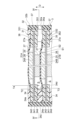
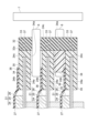
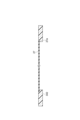
- FIG. 1 is a schematic cross-sectional view of a power storage device according to a first embodiment.
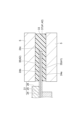
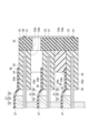
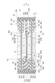
- FIG. 2 is a partially enlarged view of FIG. 1.
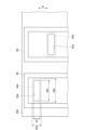
- FIG. 3 is a side view of the power storage device shown in FIG. 1.
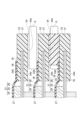
- FIG. 4 is a sectional view taken along line IV-IV in FIG. 2.
- FIG. 5 is a diagram showing steps of a method for manufacturing the power storage device shown in FIG. 1.
- FIG. 6 is a diagram showing steps of a method for manufacturing the power storage device shown in FIG. 1.
- FIG. 7 is a diagram showing steps of a method for manufacturing the power storage device shown in FIG. 1.
- FIG. 8 is a diagram showing steps of a method for manufacturing the power storage device shown in FIG. 1.
- FIG. 1 is a schematic cross-sectional view of a power storage device according to a first embodiment.
- FIG. 2 is a partially enlarged view of FIG. 1.
- FIG. 3 is a side view of the power storage device shown in FIG. 1.
- FIG. 4
- FIG. 9 is a diagram showing steps of a method for manufacturing the power storage device shown in FIG. 1.
- FIG. 10 is a diagram showing steps of a method for manufacturing the power storage device shown in FIG. 1.
- FIG. 11 is a diagram showing steps of a method for manufacturing the power storage device shown in FIG. 1.
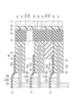
- FIG. 12 is a partially enlarged cross-sectional view of the power storage device according to the second embodiment.
- FIG. 13 is a diagram showing steps of a method for manufacturing the power storage device shown in FIG. 12.
- FIG. 14 is a diagram showing steps of a method for manufacturing the power storage device shown in FIG. 12.
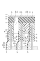
- FIG. 15 is a partially enlarged sectional view of a power storage device according to a third embodiment.
- FIG. 16 is a diagram showing steps of a method for manufacturing the power storage device shown in FIG. 15.
- FIG. 17 is a diagram showing steps of a method for manufacturing the power storage device shown in FIG. 15.
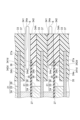
- a power storage device 1 according to the first embodiment shown in FIG. 1 is, for example, a power storage module used in a battery of a forklift, a hybrid vehicle, an electric vehicle, or the like.
- the power storage device 1 is, for example, a secondary battery such as a nickel-metal hydride secondary battery or a lithium ion secondary battery.
- power storage device 1 is a lithium ion secondary battery.
- power storage device 1 includes a laminate 2 and a sealing body 3.
- the laminate 2 includes a plurality of bipolar electrodes 21 , a positive terminal electrode 22 , and a negative terminal electrode 23 .
- the plurality of bipolar electrodes 21, positive terminal electrode 22, and negative terminal electrode 23 are stacked in the stacking direction D.
- Bipolar electrode 21 includes a current collector 24 , a positive electrode active material layer 25 , and a negative electrode active material layer 26 .
- the current collector 24 has, for example, a rectangular shape when viewed from the stacking direction D.
- Current collector 24 includes a surface 24a and a surface 24b opposite to surface 24a.
- the positive electrode active material layer 25 is provided on the surface 24a.
- the positive electrode active material layer 25 has, for example, a rectangular shape when viewed from the stacking direction D.
- the surface 24a includes an uncoated area where the positive electrode active material layer 25 is not provided.
- the uncoated area of the surface 24a surrounds the positive electrode active material layer 25 when viewed from the stacking direction D.
- the negative electrode active material layer 26 is provided on the surface 24b.
- the negative electrode active material layer 26 has, for example, a rectangular shape when viewed from the stacking direction D.
- the surface 24b includes an uncoated area where the negative electrode active material layer 26 is not provided.
- the uncoated area of the surface 24b surrounds the negative electrode active material layer 26 when viewed from the stacking direction D.
- the plurality of bipolar electrodes 21 are stacked such that the positive electrode active material layer 25 of one bipolar electrode 21 and the negative electrode active material layer 26 of the other bipolar electrode 21 face each other. That is, the plurality of bipolar electrodes 21 are arranged such that the surface 24a of the current collector 24 of one of the adjacent bipolar electrodes 21 and the surface 24b of the current collector 24 of the other bipolar electrode 21 face each other. are laminated on.
- the positive terminal electrode 22 is arranged on one side of the plurality of bipolar electrodes 21 in the stacking direction D.
- the positive terminal electrode 22 includes a current collector 24 and a positive active material layer 25 .
- the positive terminal electrode 22 differs from the bipolar electrode 21 in that it does not have the negative active material layer 26.
- the other configuration of the positive terminal electrode 22 may be the same as that of the bipolar electrode 21.
- the positive terminal electrode 22 is arranged such that the positive active material layer 25 of the positive terminal electrode 22 faces the negative active material layer 26 of the bipolar electrode 21 . That is, the positive terminal electrode 22 is stacked such that the surface 24a of the current collector 24 of the positive terminal electrode 22 and the surface 24b of the current collector 24 of the bipolar electrode 21 adjacent to the positive terminal electrode 22 face each other. .
- the negative terminal electrode 23 is arranged on the other side of the plurality of bipolar electrodes 21 in the stacking direction D.
- the negative terminal electrode 23 includes a current collector 24 and a negative active material layer 26 .
- the negative terminal electrode 23 differs from the bipolar electrode 21 in that it does not have the positive active material layer 25.
- the other configuration of the negative terminal electrode 23 may be the same as that of the bipolar electrode 21.
- the negative terminal electrode 23 is arranged such that the negative active material layer 26 of the negative terminal electrode 23 faces the positive active material layer 25 of the bipolar electrode 21 . That is, the negative terminal electrode 23 is stacked such that the surface 24b of the current collector 24 of the negative terminal electrode 23 and the surface 24a of the current collector 24 of the bipolar electrode 21 adjacent to the negative terminal electrode 23 face each other. .
- An internal space S containing an electrolytic solution is formed between each bipolar electrode 21, between the bipolar electrode 21 and the positive terminal electrode 22, and between the bipolar electrode 21 and the negative terminal electrode 23.
- the laminate 2 includes a plurality of separators 27.
- the separator 27 is arranged between each bipolar electrode 21 , between the bipolar electrode 21 and the positive terminal electrode 22 , and between the bipolar electrode 21 and the negative terminal electrode 23 .
- the separator 27 is located between the positive electrode active material layer 25 and the negative electrode active material layer 26 that face each other.
- the separator 27 has a sheet shape, for example.
- the separator 27 has, for example, a rectangular shape when viewed from the stacking direction D. When viewed from the stacking direction D, the outer edge of the separator 27 is located on the outer side of each of the outer edges of the positive electrode active material layer 25 and the outer edge of the negative electrode active material layer 26.
- the separator 27 is a member that allows charge carriers such as lithium ions to pass through. Separator 27 isolates adjacent electrodes 21, 22, and 23 from each other. This prevents electrical short circuits due to contact between the electrodes 21, 22, and 23.
- the current collector 24 is a chemically inert electrical conductor that allows current to continue flowing through the positive electrode active material layer 25 and the negative electrode active material layer 26 during discharging or charging of the lithium ion secondary battery.
- the material of the current collector 24 is, for example, a metal material, a conductive resin material, a conductive inorganic material, or the like.
- the conductive resin material include resins in which a conductive filler is added to a conductive polymer material or a non-conductive polymer material.
- the current collector 24 may include one or more layers containing the above-mentioned metal material or conductive resin material.
- a coating layer may be formed on the surface of the current collector 24 by a known method such as plating or spray coating.
- the current collector 24 may have a plate shape, a foil shape, a sheet shape, a film shape, a mesh shape, or the like, for example.
- the current collector 24 may be, for example, aluminum foil, copper foil, nickel foil, titanium foil, or stainless steel foil.
- the current collector 24 may be an alloy foil or clad foil of the above metal.
- the thickness of the current collector 24 may be in the range of 1 ⁇ m or more and 100 ⁇ m or less.
- the current collector 24 may be a laminate having a plurality of metal layers stacked in the stacking direction D.
- the current collector 24 may be a laminate in which an aluminum layer and a copper layer are integrated by, for example, plating one side of an aluminum foil with copper.
- the current collector 24 may be a laminate formed by bonding a plurality of metal foils together via a conductive adhesive.
- the current collector 24 has a first layer 241 and a second layer 242 stacked in the stacking direction D, and the first layer 241 and the second layer 242 are electrically connected. ing.
- the surface 24a of the current collector 24 is the surface of the first layer 241.
- the surface 24b of the current collector 24 is the surface of the second layer 242.
- the first layer 241 of the current collector 24 contains aluminum, and is, for example, aluminum foil.
- the second layer 242 of the current collector 24 contains copper, and is, for example, a copper foil. Note that the current collector 24 of the positive terminal electrode 22 does not need to have the second layer 242.
- the positive electrode active material layer 25 includes a positive electrode active material that can insert and release charge carriers such as lithium ions.
- the positive electrode active material include composite oxides, metallic lithium, and sulfur.
- the composition of the composite oxide includes, for example, at least one of iron, manganese, titanium, nickel, cobalt, and aluminum and lithium.
- the composite oxide include olivine-type lithium iron phosphate (LiFePO 4 ), LiCoO 2 , LiNiMnCoO 2 , and the like.
- the negative electrode active material layer 26 includes a negative electrode active material that can insert and release charge carriers such as lithium ions.
- negative electrode active materials include graphite, artificial graphite, highly oriented graphite, mesocarbon microbeads, carbon such as hard carbon and soft carbon, metal compounds, elements that can be alloyed with lithium or their compounds, boron-added carbon, etc. Can be mentioned.
- elements that can be alloyed with lithium include silicon and tin.
- Each of the positive electrode active material layer 25 and the negative electrode active material layer 26 may contain a binder and a conductive aid in addition to the active material.
- the binder plays the role of binding the active materials or conductive aids to each other and maintaining the conductive network in the electrode.
- fluororesins such as polyvinylidene fluoride, polytetrafluoroethylene, and fluororubber, thermoplastic resins such as polypropylene and polyethylene, imide resins such as polyimide and polyamideimide, alkoxysilyl group-containing resins, and polyacrylics are used.
- the conductive aid is a conductive material such as acetylene black, carbon black, graphite, etc., and can improve electrical conductivity.
- N-methyl-2-pyrrolidone or the like is used as the viscosity adjusting solvent.
- an active material layer-forming composition is prepared in the form of a slurry by mixing an active material, a solvent, and, if necessary, a binder and a conductive aid. After coating on 24a or surface 24b, it is dried.
- Solvents are, for example, N-methyl-2-pyrrolidone, methanol, methyl isobutyl ketone, water. In order to increase the electrode density, the dried material may be compressed.
- the separator 27 is, for example, a porous sheet or nonwoven fabric containing a polymer that absorbs and retains the electrolyte.
- the material of the separator 27 is, for example, polypropylene, polyethylene, polyolefin, polyester, or the like.
- the separator 27 may have a single layer structure or a multilayer structure.
- the separator 27 includes, for example, a base material layer and a pair of adhesive layers, and may be adhesively fixed to the positive electrode active material layer 25 and the negative electrode active material layer 26 by the pair of adhesive layers.
- Separator 27 may include a ceramic layer serving as a heat-resistant layer.
- the separator 27 may be reinforced with a vinylidene fluoride resin compound.
- Examples of the electrolytic solution impregnated into the separator 27 include a liquid containing a non-aqueous solvent and an electrolyte salt dissolved in the non-aqueous solvent.
- the electrolyte salt of the electrolytic solution known lithium salts such as LiClO 4 , LiAsF 6 , LiPF 6 , LiBF 4 , LiCF 3 SO 3 , LiN(FSO 2 ) 2 , LiN(CF 3 SO 2 ) 2 and the like can be used.
- the nonaqueous solvent known solvents such as cyclic carbonates, cyclic esters, chain carbonates, chain esters, and ethers can be used. Note that two or more of these known solvent materials may be used in combination.
- the sealing body 3 is a member that seals the internal space S.
- the sealing body 3 is provided on the side surface of the laminate 2 .
- the sealing body 3 seals the side surface of the laminate 2 .
- the sealing body 3 has a rectangular cylindrical shape, for example.
- the sealing body 3 has electrical insulation properties.
- the sealing body 3 has a main body portion 31 and a welded portion 32.
- the main body portion 31 is provided at the outer edge of the laminate 2 .
- the main body portion 31 is composed of a plurality of independent members.
- the main body part 31 has a plurality of seal parts 33 and a plurality of spacers 34.
- the seal portion 33 includes a seal portion 35 provided on the surface 24a of the current collector 24, a seal portion 36 provided on the surface 24b of the current collector 24, and a seal portion 37 provided on the side surface of the current collector 24. It has .
- Each seal portion 35, 36 has a rectangular frame shape, for example, when viewed from the stacking direction.
- the seal portion 35 surrounds the positive electrode active material layer 25 and the negative electrode active material layer 26 when viewed from the stacking direction D.
- An inner edge 35d of the seal portion 35 is separated from the positive electrode active material layer 25.
- the outer edge 35c of the seal portion 35 substantially coincides with the outer edge 24c of the current collector 24 when viewed from the stacking direction D.
- Seal portion 35 is welded to surface 24a.
- the seal portion 36 surrounds the positive electrode active material layer 25 and the negative electrode active material layer 26 when viewed from the stacking direction D.
- An inner edge 36d of the seal portion 36 is separated from the negative electrode active material layer 26.
- the inner edge 36d of the seal portion 36 substantially coincides with the inner edge 35d of the seal portion 35 when viewed from the stacking direction D.
- the outer edge 36c of the seal portion 36 substantially coincides with the outer edge 24c of the current collector 24 when viewed from the stacking direction D. Seal portion 36 is welded to surface 24b.
- the seal portion 37 is provided on the side surface of the current collector 24.
- the seal portion 37 covers the side surface of the current collector 24.
- the seal portion 37 is welded to the side surface of the current collector 24.
- the seal portion 37 seals between the first layer 241 and the second layer 242.
- the seal portion 37 is connected to an outer edge 35c of the seal portion 35 and an outer edge 36c of the seal portion 36, respectively.
- the seal portions 35, 36, and 37 are part of the seal portion 33 integrally formed of the same material.
- the spacer 34 has, for example, a rectangular frame shape (see FIG. 4) with a portion cut out for a liquid injection port 34a to be described later.
- the spacer 34 is provided between a pair of adjacent seal portions 33 in the stacking direction D.
- the inner edge 34d of the spacer 34 is located on the opposite side of the positive electrode active material layer 25 or the negative electrode active material layer 26 with respect to the inner edge 35d of the seal portion 35 and the inner edge 36d of the seal portion 36, respectively, when viewed from the stacking direction. You may do so. That is, the inner edge 34d of the spacer 34 may be located further away from the positive electrode active material layer 25 or the negative electrode active material layer 26 than the inner edge 35d of the seal portion 35 and the inner edge 36d of the seal portion 36.
- the outer edge 34c of the spacer 34 substantially coincides with the outer edge 33c of the seal portion 33 when viewed from the stacking direction D.
- the inner edge 34d of the spacer 34 may be located closer to the positive electrode active material layer 25 or the negative electrode active material layer 26 than the inner edge 35d of the seal portion 35 and the inner edge 36d of the seal portion 36.
- each of the seal portion 33 and the spacer 34 is, for example, acid-modified polyethylene (acid-modified PE), acid-modified polypropylene (acid-modified PP), polyethylene, or polypropylene.
- Each of the seal portion 33 and the spacer 34 has electrolyte resistance.
- the materials of the seal portion 33 and the spacer 34 may be the same or different.
- the material of the seal portion 33 is, for example, acid-modified polyethylene or acid-modified polypropylene.
- the material of the spacer 34 is, for example, polyethylene or polypropylene.
- Acid-modified polyethylene and acid-modified polypropylene are easier to bond to metals than non-acid-modified polyethylene and non-acid-modified polypropylene.
- the bonding strength of the seal portions 35, 36 to the current collector 24 can be improved by forming the seal portions 35, 36 from acid-modified polyethylene or acid-modified polypropylene.
- the welded part 32 is provided on the outside of the main body part 31.
- the welded portion 32 is integrated by welding the outer edges of each seal portion 33 and each spacer 34 .
- the welded portion 32 has, for example, a rectangular cylindrical shape.
- the welded portion 32 extends continuously in the stacking direction D from one end of the stacked body 2 to the other end.
- each seal portion 33 and each A welded portion 32 is formed by welding the outer edges of each of the spacers 34.
- the welded portion 32 may be formed such that the inner edge of the welded portion 32 does not overlap each current collector 24 when viewed from the stacking direction D.
- power storage device 1 includes a first electrode 21A and a second electrode 21B adjacent to the first electrode 21A.
- the first electrode 21A and the second electrode 21B are a pair of mutually adjacent bipolar electrodes 21 shown in FIG.
- the first electrode 21A has a first current collector 24A
- the second electrode 21B has a second current collector 24B.
- Each of the first current collector 24A and the second current collector 24B is the current collector 24 shown in FIG.
- Each of the first current collector 24A and the second current collector 24B includes a first surface 24d and a second surface 24e.
- the first surface 24d is the surface 24a shown in FIG. 1, and the second surface 24e is the surface 24b shown in FIG.
- the main body portion 31 has a first seal portion 331 and a second seal portion 332.
- the first seal portion 331 is provided on the first current collector 24A
- the second seal portion 332 is provided on the second current collector 24B.
- Each of the first seal portion 331 and the second seal portion 332 is the seal portion 33 shown in FIG.
- the first seal portion 331 includes a first seal portion 351.
- the first seal portion 351 is welded to the first surface 24d of the first current collector 24A.
- the first seal portion 351 is the seal portion 35 shown in FIG.
- the second seal portion 332 includes a second seal portion 362.
- the second seal portion 362 is welded to the second surface 24e of the second current collector 24B.
- Second seal portion 362 is seal portion 36 shown in FIG.
- the spacer 34 together with the first electrode 21A, the first seal portion 331, the second electrode 21B, and the second seal portion 332, forms an internal space S for accommodating the electrolyte.
- the spacer 34 is sandwiched between a first seal portion 351 and a second seal portion 362.
- the spacer 34 is a separate member from the first seal part 331 and the second seal part 332.
- the spacer 34 is in contact with each of the first seal portion 351 and the second seal portion 362.
- the spacer 34 is not welded to each of the first seal portion 351 and the second seal portion 362.
- the thickness T1 of the spacer 34 is larger than the thickness T2 of the first seal portion 351 and the thickness T3 of the second seal portion 362, respectively.
- the thickness T1 of the spacer 34 is, for example, twice or more the thickness T2 of the first seal portion 351 or the thickness T3 of the second seal portion 362.
- the thickness T1 of the spacer 34 is smaller than the thickness T4 of the first seal portion 331 or the second seal portion 332. That is, the thickness T1 of the spacer 34 is smaller than the sum of the thickness of the current collector 24, the thickness T2 of the first seal portion 351, and the thickness T3 of the second seal portion 362. Note that the thickness T2 of the first seal portion 351 and the thickness T3 of the second seal portion 362 may be the same or different.
- the peripheral edge 27a of the separator 27 is located between the spacer 34 and the second seal portion 362.
- the peripheral edge 27a of the separator 27 may be sandwiched between the spacer 34 and the second seal portion 362 in a region excluding a liquid injection port 34a, which will be described later.
- the peripheral edge portion 27a of the separator 27 may be welded and fixed to the second seal portion 362.
- the separator 27 divides the internal space S into a first region S1 and a second region S2.
- the first region S1 is a region in the internal space S between the separator 27 and the first electrode 21A.
- the second region S2 is a region of the internal space S between the separator 27 and the second electrode 21B.
- the volume of the first region S1 is larger than the volume of the second region S2.
- the area of the positive electrode active material layer 25 is smaller than the area of the negative electrode active material layer 26.
- the outer edge of the positive electrode active material layer 25 is located inside the outer edge of the negative electrode active material layer 26.
- a plurality of grooves 25a are formed in the positive electrode active material layer 25.
- the peripheral edge 27a of the separator 27 is located between the spacer 34 and the second seal portion 362.
- the volume of the first region S1 is larger than the volume of the second region S2.
- the thickness of the positive electrode active material layer 25 may be greater than the thickness of the negative electrode active material layer 26. In this case, the volume of the first region S1 becomes even larger than the volume of the second region S2.
- the spacer 34 includes a liquid injection port (first liquid injection port) 34a.
- the liquid injection port 34a penetrates the spacer 34.
- the liquid injection port 34a opens at each of the outer edge 34c and the inner edge 34d of the spacer 34.
- the liquid injection port 34a communicates with the internal space S.
- the liquid injection port 34a functions as a path for injecting the electrolyte into the internal space S.
- the liquid injection ports 34a of the plurality of spacers 34 may be formed at different positions when viewed from the stacking direction D. As an example, the liquid injection ports 34a of the plurality of spacers 34 lined up in the stacking direction D are arranged diagonally with respect to the stacking direction D.
- the respective liquid injection ports 34a communicating with the internal spaces S adjacent to each other in the stacking direction D are arranged at shifted positions so as not to overlap each other when viewed from the stacking direction D.
- the liquid injection port 34a has, for example, a rectangular shape when viewed from a direction intersecting the outer surface 32b of the welded portion 32.
- the welded part 32 includes a plurality of liquid injection ports (second liquid injection ports) 32a.
- the liquid injection port 32a penetrates the welded portion 32.
- the liquid injection port 32a opens on the outer surface 32b of the welded portion 32.
- the liquid inlet 32a communicates with the liquid inlet 34a.
- the liquid injection port 32a functions as a path for injecting the electrolyte into the internal space S via the liquid injection port 34a.
- Each liquid injection port 32a is arranged diagonally with respect to the stacking direction D, similarly to the liquid injection port 34a.
- the respective liquid injection ports 32a communicating with the internal spaces S adjacent to each other in the stacking direction D are arranged at shifted positions so as not to overlap each other when viewed from the stacking direction D.
- the liquid injection port 32a has, for example, a rectangular shape when viewed from a direction intersecting the outer surface 32b of the welded portion 32.
- the area of the liquid inlet 32a is smaller than the area of the liquid inlet 34a.
- the liquid inlet 32a may be located inside the liquid inlet 34a, for example.
- the width W1 of the liquid injection port 32a in the stacking direction D is smaller than the width W2 of the liquid injection port 34a in the stacking direction D.
- the width W3 of the liquid inlet 32a in the direction intersecting the stacking direction D is smaller than the width W4 of the liquid inlet 34a in the direction intersecting the stacking direction D.
- a frame portion 38 surrounding the liquid injection port 32a is formed on the outer surface 32b.
- the frame portion 38 protrudes from the outer surface 32b.
- the frame portion 38 has a rectangular frame shape, for example, when viewed from a direction intersecting the outer surface 32b.
- the inner edge of the frame portion 38 is located on the outer side of the liquid inlet 32a and the liquid inlet 34a.
- the inner region of the frame portion 38 communicates with the liquid injection port 34a via the liquid injection port 32a.
- the positive electrode active material layer 25 includes a plurality of grooves 25a.
- Each groove 25a extends in the direction in which the liquid inlet 32a, the liquid inlet 34a, and the internal space S are lined up.
- Each groove 25a reaches both ends of the positive electrode active material layer 25 in the extending direction of the groove 25a.
- the depth of each groove 25a in the stacking direction D is the same as the thickness of the positive electrode active material layer 25 in the stacking direction D. That is, each groove 25a is formed in the stacking direction D to reach the first surface 24d of the first current collector 24A.
- the first surface 24d of the first current collector 24A is exposed in each groove 25a.
- Each groove 25a is a part of the first region S1.
- the electrolytic solution injected from the liquid injection ports 32a and 34a can move through the region between the positive electrode active material layer 25 and the spacer 34 and each groove 25a in the first region S1.
- the bipolar electrode 21, the seal member 41, and the seal member 42 are prepared. Subsequently, the seal member 41 is placed on the surface 24a of the current collector 24, and the seal member 42 is placed on the surface 24b of the current collector 24.
- the sealing member 41 and the sealing member 42 are arranged so as to protrude from the outer edge 24c of the current collector 24, respectively. That is, when viewed from the stacking direction D, the sealing member 41 disposed on the surface 24a of the current collector 24 and the sealing member 42 disposed on the surface 24b of the current collector 24 are connected to the current collector 24, respectively. It has an overlapping portion and a portion that does not overlap with the current collector 24.
- each of the sealing member 41 and the sealing member 42 are heated by the heater 5.
- the heater 5 is, for example, an impulse sealer. Heating of the sealing member 41 and the sealing member 42 is performed with the heater 5 sandwiching the current collector 24 via the sealing member 41 and the sealing member 42, respectively. As a result, a portion of the seal member 41 that overlaps with the surface 24a is welded to the surface 24a, thereby forming a seal portion 35, and a portion of the seal member 42 that overlaps with the surface 24b is welded to the surface 24b. A seal portion 36 is thereby formed.
- seal portion 33 is formed on the bipolar electrode 21.
- a seal portion 33 is also formed on the positive terminal electrode 22 and the negative terminal electrode 23 by a similar process.
- each electrode 21, 22, 23 with a seal portion 33 formed thereon and each spacer 34 are stacked.
- a spacer 34 is arranged between each seal portion 33 .
- the liquid injection port forming member 6 is inserted into the liquid injection port 34a of the spacer 34.
- the liquid injection port forming member 6 has a plate shape, for example.
- the liquid injection port forming member 6 extends from the outside of the spacer 34 to the internal space S.
- the width of the liquid injection port forming member 6 is smaller than the width of the liquid injection port 34a. That is, a clearance exists between the liquid injection port forming member 6 and the liquid injection port 34a.
- the heating device 7 is, for example, an infrared heater.
- the heating device 7 irradiates the outer surfaces of each seal portion 33 and each spacer 34 with infrared rays.
- the temperature of each seal portion 33 and each spacer 34 increases.
- the heating of each seal portion 33 and each spacer 34 is controlled by the heating device 7 so that the temperature thereof is equal to or higher than the melting point. As a result, the outer edges of each seal portion 33 and each spacer 34 are melted.
- each seal portion 33 and each spacer 34 When the outer edges of each seal portion 33 and each spacer 34 are melted, the melted liquid portion flows to fill the gap between the liquid injection port 34a and the liquid injection port forming member 6. When heating by the heating device 7 is stopped, the melted outer edges of each seal portion 33 and each spacer 34 cool and solidify to become a welded portion 32.
- each liquid injection port forming member 6 is pulled out from the liquid injection port 34a.
- a liquid injection port 32a is formed in the welded portion 32.
- the frame portion 38 is formed on the outer surface 32b of the welded portion 32 by, for example, injection molding.
- the electrolytic solution is injected into each internal space S through each liquid injection port 32a and each liquid injection port 34a.
- the equipment side nozzle 8 is pressed against the frame portion 38.
- the equipment side nozzle 8 has a support member 81 and a seal member 82.
- the seal member 82 is provided on the surface of the support member 81.
- the seal member 82 is, for example, an elastic body.
- the seal member 82 is, for example, a packing.
- a plurality of liquid injection ports 8a are formed in the equipment side nozzle 8. Each liquid injection port 8a corresponds to each liquid injection port 32a and each liquid injection port 34a. The surface of the seal member 82 is pressed against the frame portion 38.
- the seal member 82 When the surface of the seal member 82 is pressed against the frame portion 38, at least a portion of the frame portion 38 bites into the seal member 82. Thereby, the space between the frame portion 38 and the seal member 82 is sealed. Subsequently, the electrolytic solution is injected into the internal space S using the equipment side nozzle 8.
- each liquid injection port 32a is sealed. Specifically, by joining the sealing material 9 to the frame 38, the liquid injection port 32a surrounded by the frame 38 is sealed. Thereby, power storage device 1 shown in FIG. 1 is manufactured. Note that in FIG. 1, illustration of the frame portion 38 and the sealing material 9 is omitted.
- the first seal portion 351 is welded to the first surface 24d of the first current collector 24A, and the second seal portion 351 is welded to the second surface 24e of the second current collector 24B. 362 is welded. Furthermore, the welded portion 32 is formed by welding the outer edges of each seal portion 33 and each spacer 34 . Thereby, the internal space S can be reliably sealed. Further, the thickness T1 of the spacer 34 is larger than each of the thickness T2 of the first seal portion 351 and the thickness T3 of the second seal portion 362, and the liquid injection port 34a is formed in the spacer 34. .
- the sealing body 3 that defines the internal space S together with the electrodes disposed opposite to each other a sufficient thickness in the stacking direction D of the spacer 34 for forming the liquid injection port 34a is ensured, and the first set of The thickness in the stacking direction D of the first seal portion 351 welded to the electric body 24A or the second seal portion 362 welded to the second current collector 24B can be made sufficiently small. Therefore, according to the power storage device 1, the deformation (for example, wrinkles, etc.) of the first current collector 24A due to welding of the first seal portion 351 to the first surface 24d, or the deformation of the second seal portion to the second surface 24e.
- the width in the stacking direction D of the liquid injection port 34a, which serves as a flow path when injecting the electrolyte, can be increased, and the electrolyte can be efficiently injected into the internal space S. Can be done.
- the width of the liquid inlet 32a is smaller than the width of the liquid inlet 34a. Thereby, backflow of the electrolytic solution accommodated in the internal space S to the outside can be suppressed.
- the peripheral edge 27a of the separator 27 is fixed to the seal portion 36.
- the volume of the first region S1 of the interior space S is larger than the volume of the second region S2 of the interior space S.
- the area of the positive electrode active material layer 25 is smaller than the area of the negative electrode active material layer 26.
- the volume of the first region S1 can be made larger than the volume of the second region S2, and as described above, smooth liquid injection can be realized.
- the thickness of the positive electrode active material layer 25 is greater than the thickness of the negative electrode active material layer 26. Thereby, the volume of the first region S1 can be made larger than the volume of the second region S2, and as described above, smooth liquid injection can be realized.
- the positive electrode active material layer 25 includes a groove 25a extending in the direction in which the liquid injection port 34a and the internal space S are lined up. This prevents the flow of the electrolytic solution from being obstructed by the positive electrode active material layer 25, so that smooth injection can be achieved. In addition, since the grooves 25a reach the surface 24a of the current collector 24, gases generated during the formation of the positive electrode active material layer 25 on the surface 24a are efficiently removed from between the surface 24a and the positive electrode active material layer 25. It can be discharged well.
- the current collector 24 has a first layer 241 and a second layer 242.
- the seal portion 33 includes a seal portion 35 welded to the surface 24a, a seal portion 36 welded to the surface 24b, and a seal portion 37 welded to the side surface of the current collector 24.
- the seal length between the first layer 241 and the seal portion 33 is ensured, so that the electrolyte is distributed between the seal portion 35 and the surface 24a of the first layer 241 and between the seal portion 37 and the side surface of the first layer 241. It is possible to prevent the second layer 242 from coming into contact with the second layer 242 after entering between the two layers.
- the electrolyte is allowed to flow between the seal portion 36 and the surface 24b of the second layer 242 and between the seal portion 37 and the side surface of the second layer 242. It is possible to prevent the first layer 241 from coming into contact with the first layer 241 after entering between the two layers.
- the power storage device of the second embodiment mainly differs from the power storage device 1 of the first embodiment in that it includes a spacer 34A instead of the spacer 34.
- the spacer 34A is provided between the first seal part 331 and the second seal part 332.
- the spacer 34A includes a first spacer 341 and a second spacer 342. Each of the first spacer 341 and the second spacer 342 is a separate member.
- the first spacer 341 has, for example, a rectangular frame shape with a portion cut out for a liquid injection port 34a to be described later.
- the first spacer 341 is in contact with the first seal portion 351 of the first seal portion 331 .
- the first spacer 341 is not welded to the first seal portion 351.
- the inner edge 341d of the first spacer 341 is located on the opposite side of the positive electrode active material layer 25 with respect to the inner edge 35d of the first seal portion 351 when viewed from the stacking direction D. That is, the inner edge 341d of the first spacer 341 is located further away from the positive electrode active material layer 25 than the inner edge 35d of the first seal portion 351.
- the first spacer 341 includes a liquid injection port (first liquid injection port) 34a. That is, the liquid injection port 34a is formed in the first spacer 341.
- the liquid injection port 34a penetrates the first spacer 341.
- the liquid injection port 34a opens at each of the outer edge and inner edge 341d
- the second spacer 342 has a rectangular frame shape, for example.
- the second spacer 342 is provided between the first spacer 341 and the second seal portion 332.
- the second spacer 342 is in contact with the first spacer 341.
- the second spacer 342 is in contact with the second seal portion 362 of the second seal portion 332 .
- the second spacer 342 is not welded to the second seal portion 362.
- the inner edge 342d of the second spacer 342 is located on the opposite side of the negative electrode active material layer 26 with respect to the inner edge 36d of the second seal portion 362 when viewed from the stacking direction D. That is, the inner edge 342d of the second spacer 342 is located further away from the negative electrode active material layer 26 than the inner edge 36d of the second seal portion 362.
- the inner edge 342d of the second spacer 342 substantially coincides with the inner edge 341d of the first spacer 341 when viewed from the stacking direction D.
- the second spacer 342 does not include a liquid injection port.
- the second spacer 342 has a frame shape that is continuously connected in the circumferential direction.
- the thickness T11 of the first spacer 341 is larger than the thickness T2 of the first seal portion 351 and the thickness T3 of the second seal portion 362, respectively.
- the thickness T12 of the second spacer 342 is larger than the thickness T2 of the first seal portion 351 and the thickness T3 of the second seal portion 362, respectively.
- the thickness T11 of the first spacer 341 and the thickness T12 of the second spacer 342 are the same. That is, each of the thickness T11 of the first spacer 341 and the thickness T12 of the second spacer 342 is about half the thickness T1 of the spacer 34A.
- the thickness T11 of the first spacer 341 and the thickness T12 of the second spacer 342 may be different.
- the thickness T11 of the first spacer 341 may be greater than the thickness T12 of the second spacer 342.
- the thickness T11 of the first spacer 341 may be smaller than the thickness T12 of the second spacer 342.
- the thickness T11 of the first spacer 341 may be less than or equal to the thickness T2 of the first seal portion 351 or the thickness T3 of the second seal portion 362.
- the thickness T12 of the second spacer 342 may be less than or equal to the thickness T2 of the first seal portion 351 or the thickness T3 of the second seal portion 362.
- the peripheral edge 27a of the separator 27 is located between the first spacer 341 and the second spacer 342.
- the peripheral edge 27a of the separator 27 is welded to the second spacer 342.
- the peripheral edge 27a of the separator 27 is welded to the surface of the second spacer 342 that faces the first spacer 341.
- the peripheral edge 27a of the separator 27 is welded to the second spacer 342 over the entire circumference of the second spacer 342. That is, the portion of the separator 27 that is welded to the second spacer 342 has a rectangular frame shape when viewed from the stacking direction D.
- seal portions 33 are formed on each electrode 21, 22, 23 (see FIGS. 5 and 6).
- the peripheral edge 27a of the separator 27 is welded to the second spacer 342. Specifically, after the peripheral edge 27a of the separator 27 is placed on one side of the second spacer 342, the peripheral edge 27a of the separator 27 and the second spacer 342 are heated.
- the electrodes 21, 22, 23 on which the seal portion 33 is formed, the second spacer 342 and the first spacer 341 on which the separator 27 is welded are stacked.
- the first spacer 341 is arranged on one side of the second spacer 342 to which the peripheral edge 27a of the separator 27 is welded.
- the first spacer 341 and the second spacer 342 are arranged between each seal portion 33.
- the liquid injection port forming member 6 is inserted into the liquid injection port 34a.
- formation of a welded portion, injection of an electrolytic solution, sealing of a liquid injection port, etc. are performed. In this way, the power storage device of the second embodiment is manufactured.
- the spacer 34A includes a first spacer 341 and a second spacer 342, each of which is formed into a frame shape and stacked in the stacking direction D. This makes it easy to adjust the thickness of spacer 34A, making it easy to manufacture the power storage device. Further, since the spacer 34A includes a plurality of spacers, the thickness of each spacer 341, 342 is smaller than the distance between adjacent seal parts 33, and as a result, it is thinner than when a single spacer is used. can do. This makes it easier to wind the precursors of the spacers 341 and 342 into a roll, for example. Therefore, the precursors of the spacers 341 and 342 can be easily handled, and as a result, the power storage device can be manufactured easily.
- the peripheral edge 27a of the separator 27 is welded to the second spacer 342.
- the separator 27 is not welded to the first spacer 341 in the region of the first spacer 341 where the liquid injection port 34a is formed. Fixation may be insufficient.
- the peripheral edge 27a of the separator 27 is welded to the second spacer 342 in which the liquid injection port 34a is not formed. can be fixed to. Therefore, short circuit between each electrode 21, 22, 23 can be suppressed.
- the separator 27 When the separator 27 is welded to the first seal portion 351 or the second seal portion 362, after welding the first seal portion 351 or the second seal portion 362 to the current collector 24, the separator 27 is welded to the first seal portion 351 or the second seal portion 362. It may be welded to the portion 351 or the second seal portion 362. In such a case, since the first seal portion 351 or the second seal portion 362 is heated multiple times, the welding strength of the first seal portion 351 or the second seal portion 362 to the current collector 24 is reduced. There is a risk of it getting lost.
- the peripheral edge 27a of the separator 27 is welded to the second spacer 342, so that the first seal portion 351 or the second seal portion 362 is connected to the current collector 24. Decrease in welding strength is suppressed.
- the power storage device of the third embodiment differs from the power storage device of the second embodiment mainly in that it includes a spacer 34B instead of spacer 34A. As shown in FIG. 15, the spacer 34B is provided between the first seal part 331 and the second seal part 332.
- the spacer 34B includes a first spacer 341, a second spacer 342, and a third spacer 343. Each of the first spacer 341, second spacer 342, and third spacer 343 is a separate member.
- the thickness T11 of the first spacer 341 is approximately 1 ⁇ 3 of the thickness T1 of the spacer 34B.
- the other points of the first spacer 341 are the same as the first spacer 341 of the second embodiment.
- the second spacer 342 is provided between the first spacer 341 and the third spacer 343.
- the thickness T12 of the second spacer 342 is the same as the thickness T11 of the first spacer 341. That is, the thickness T12 of the second spacer 342 is about 1 ⁇ 3 of the thickness T1 of the spacer 34B.
- the inner edge 342d of the second spacer 342 is located inside the inner edge 341d of the first spacer 341 when viewed from the stacking direction D.
- the inner edge 342d of the second spacer 342 is located inside the inner edge 35d of the first seal portion 351 or the inner edge 36d of the second seal portion 362 when viewed from the stacking direction D.
- the width of the side portion of the second spacer 342 is greater than the width of the side portion of the first spacer 341.
- the other points of the second spacer 342 are the same as the second spacer 342 of the second embodiment.
- the third spacer 343 is stacked on the side opposite to the first spacer 341 with respect to the second spacer 342.
- the third spacer 343 has a rectangular frame shape, for example.
- the thickness T13 of the third spacer 343 is the same as the thickness T11 of the first spacer 341. That is, the thickness T13 of the third spacer 343 is about 1 ⁇ 3 of the thickness T1 of the spacer 34B.
- the third spacer 343 is in contact with the second seal portion 362 of the second seal portion 332 .
- the third spacer 343 is not welded to the second seal portion 362.
- the inner edge 343d of the third spacer 343 is located on the opposite side of the negative electrode active material layer 26 with respect to the inner edge 36d of the second seal portion 362 when viewed from the stacking direction D.
- the inner edge 343d of the third spacer 343 substantially coincides with the inner edge 341d of the first spacer 341 when viewed from the stacking direction D.
- the third spacer 343 includes a liquid injection port (first liquid injection port) 34a. That is, the liquid injection port 34a is also formed in the third spacer 343. The liquid injection port 34a passes through the third spacer 343. The liquid injection port 34a opens at each of the outer edge and inner edge 343d of the third spacer 343.
- the thickness T11 of the first spacer 341, the thickness T12 of the second spacer 342, and the thickness T13 of the third spacer 343 are each different from the thickness T2 of the first seal portion 351 and the thickness T3 of the second seal portion 362. greater than each.
- the thickness T11 of the first spacer 341, the thickness T12 of the second spacer 342, and the thickness T13 of the third spacer 343 may be different from each other similarly to the power storage device of the second embodiment.
- the thickness T13 of the third spacer 343 may be less than or equal to the thickness T2 of the first seal portion 351 or the thickness T3 of the second seal portion 362.
- the peripheral edge 27a of the separator 27 is welded to the second spacer 342.
- the peripheral edge 27a of the separator 27 is welded to the surface of the second spacer 342 that faces the first spacer 341.
- the peripheral edge 27a of the separator 27 is welded to a portion of the second spacer 342 that is inside the first spacer 341.
- the peripheral edge 27a of the separator 27 is welded to the second spacer 342 over the entire circumference of the second spacer 342. That is, the portion of the separator 27 that is welded to the second spacer 342 has a rectangular frame shape when viewed from the stacking direction D. Note that the peripheral edge portion 27a of the separator 27 may extend between the first spacer 341 and the second spacer 342.
- seal portions 33 are formed on each electrode 21, 22, 23 (see FIGS. 5 and 6).
- the peripheral edge 27a of the separator 27 is welded to the second spacer 342. Specifically, after the peripheral edge 27a of the separator 27 is placed on one side of the second spacer 342, the peripheral edge 27a of the separator 27 and the second spacer 342 are heated.
- the electrodes 21, 22, 23 on which the seal portion 33 is formed, the second spacer 342 on which the separator 27 is welded, the first spacer 341, and the third spacer 343 are stacked.
- the first spacer 341 is arranged on one side of the second spacer 342 to which the peripheral edge 27a of the separator 27 is welded.
- the third spacer 343 is arranged on the opposite side of the first spacer 341 with respect to the second spacer 342 .
- the first spacer 341 , the second spacer 342 , and the third spacer 343 are arranged between each seal portion 33 .
- the liquid injection port forming member 6 is inserted into the liquid injection port 34a.
- formation of a welded portion, injection of an electrolytic solution, sealing of a liquid injection port, etc. are performed. In this way, the power storage device of the third embodiment is manufactured.
- the inner edge 342d of the second spacer 342 is located inside the inner edge 341d of the first spacer 341. Thereby, a sufficient area of the second spacer 342 for welding the separator 27 can be secured. Therefore, the peripheral edge 27a of the separator 27 can be fixed more reliably, and short circuits between the electrodes 21, 22, 23 can be more reliably suppressed.
- the spacer 34B includes a third spacer 343 stacked on the opposite side of the first spacer 341 to the second spacer 342.
- the liquid injection port 34a is formed in each of the first spacer 341 and the third spacer 343. Thereby, liquid can be injected from both sides of the separator 27 in the stacking direction D. Therefore, smooth liquid injection can be achieved.
- the first electrode 21A is the positive terminal electrode 22
- the second electrode 21B is the bipolar electrode 21 adjacent to the positive terminal electrode 22.
- attention may be paid to the negative terminal electrode 23 and the bipolar electrode 21 adjacent to the negative terminal electrode 23.
- the first electrode 21A is the bipolar electrode 21 adjacent to the negative terminal electrode 23, and the second electrode 21B is the negative terminal electrode 23.
- the current collector 24 has the first layer 241 and the second layer 242, but the current collector 24 may have only one layer.
- the peripheral edge 27a of the separator 27 is welded to the surface of the second spacer 342 that faces the first spacer 341, but the peripheral edge 27a of the separator 27 is , may be welded to the surface of the second spacer 342 opposite to the first spacer 341.
- an example was shown in which the peripheral edge part 27a of the separator 27 is welded to the second spacer 342 over the entire circumference of the second spacer 342, but the peripheral edge part of the separator 27 27a may be welded to the second spacer 342 at predetermined intervals in the circumferential direction of the second spacer 342.
- the peripheral edge 27a of the separator 27 may be partially welded to the second spacer 342. Even in this case, the separator 27 can be welded to the second spacer 342 at intervals independent of the width of the liquid injection port 34a, so the peripheral edge 27a of the separator 27 can be reliably fixed. Note that in the second embodiment and the third embodiment, the separator 27 does not need to be welded to the spacers 34A, 34B. In the second embodiment and the third embodiment, the peripheral edge 27a of the separator 27 may be welded to the first seal portion 351 or the second seal portion 362. In the second embodiment and the third embodiment, the separator 27 does not need to be welded.
- the gist of the present disclosure is as follows [1] to [10].
- a laminate including a first electrode and a second electrode laminated in a stacking direction, and a sealing body for sealing a side surface of the laminate, wherein the first electrode has a first surface. and a positive electrode active material layer provided on the first surface, and the second electrode has a second current collector including a second surface opposite to the first surface. and a negative electrode active material layer provided on the second surface, and the sealing body is welded to the first surface so as to surround the positive electrode active material layer when viewed from the stacking direction.
- a first seal portion including a first seal portion; a second seal portion including a second seal portion welded to the second surface so as to surround the negative electrode active material layer when viewed from the stacking direction; a spacer sandwiched between the first seal portion and the second seal portion; and the spacer located outside the respective outer edges of the first current collector and the second current collector when viewed from the stacking direction.
- a welded part formed by welding outer edges of each of the first seal part, the second seal part, and the spacer, and the spacer includes the first electrode, the second electrode, and the sealing body.
- the welded portion includes a first liquid inlet that is formed by the spacer and communicates with an internal space in which an electrolytic solution is accommodated, and the welded part includes a second liquid inlet that communicates with the first liquid inlet, and the welded part includes a second liquid inlet that communicates with the first liquid inlet, and
- the power storage device has a thickness larger than each of the first seal portion and the second seal portion.
- the power storage device according to [7] Further comprising a separator provided between the positive electrode active material layer and the negative electrode active material layer, the first liquid injection port is formed in the first spacer, and the peripheral edge of the separator is , the power storage device according to [7], which is welded to the second spacer.
- the spacer further includes a third spacer stacked on a side opposite to the first spacer with respect to the second spacer, and the first liquid inlet is connected to the first spacer and the third spacer.
- SYMBOLS 1 Power storage device, 2... Laminated body, 3... Sealing body, 21... Bipolar electrode, 24... Current collector, 24a, 24b... Surface, 25... Positive electrode active material layer, 25a... Groove, 26... Negative electrode active material layer , 27... Separator, 27a... Peripheral part, 32... Welding part, 34... Spacer, 32a, 34a... Liquid inlet, 33... Seal part, 35, 36... Seal part, 341... First spacer, 342... Second spacer , 343...Third spacer, S...Internal space, S1...First region, S2...Second region.
Landscapes
- Chemical & Material Sciences (AREA)
- Chemical Kinetics & Catalysis (AREA)
- Electrochemistry (AREA)
- General Chemical & Material Sciences (AREA)
- Engineering & Computer Science (AREA)
- Manufacturing & Machinery (AREA)
- Materials Engineering (AREA)
- Physics & Mathematics (AREA)
- Condensed Matter Physics & Semiconductors (AREA)
- General Physics & Mathematics (AREA)
- Inorganic Chemistry (AREA)
- Secondary Cells (AREA)
Abstract
蓄電装置は、積層体と、積層体の側面を封止するための封止体と、を備えている。封止体は、第1集電体の第1表面に溶着された第1シール部分と、第2集電体の第2表面に溶着された第2シール部分と、第1シール部分及び第2シール部分によって挟まれたスペーサと、集電体の外縁よりも外側に位置する各シール部及びスペーサのそれぞれの外縁部の溶着によって形成された溶着部と、を有している。スペーサは、内部空間に連通する第1注液口を含んでいる。溶着部は、第1注液口に連通する第2注液口を含んでいる。スペーサの厚さは、第1シール部分の厚さ及び第2シール部分の厚さのそれぞれよりも大きい。
Description
本開示は、蓄電装置に関する。
従来、複数の電極を含む積層体、及び、積層体の側面を封止するための封止体を備える蓄電装置が知られている(例えば、特許文献1参照)。このような蓄電装置では、封止体は、電極の集電体の一方面に溶着されたシール部を含む部材を有している。シール部には、内部空間へ電解液を注入するための注液口が形成されている。
上述したような蓄電装置では、シール部に注液口を形成するために、シール部の厚さを比較的大きくすることが求められる場合がある。しかし、シール部の厚さが大きくなると、シール部が集電体の一方面に溶着される際に、シール部の熱収縮に起因して集電体が変形してしまうおそれがある。
本開示は、集電体の変形を抑制することができる蓄電装置を提供することを目的とする。
本開示の蓄電装置は、積層方向に積層された第1電極及び第2電極を含む積層体と、積層体の側面を封止するための封止体と、を備え、第1電極は、第1表面を含む第1集電体と、第1表面に設けられた正極活物質層と、を有し、第2電極は、第1表面に対向する第2表面を含む第2集電体と、第2表面に設けられた負極活物質層と、を有し、封止体は、積層方向から見た場合に正極活物質層を囲むように第1表面に溶着された第1シール部分を含む第1シール部と、積層方向から見た場合に負極活物質層を囲むように第2表面に溶着された第2シール部分を含む第2シール部と、第1シール部分及び第2シール部分によって挟まれたスペーサと、積層方向から見た場合に第1集電体及び第2集電体のそれぞれの外縁よりも外側に位置する第1シール部、第2シール部及びスペーサのそれぞれの外縁部の溶着によって形成された溶着部と、を有し、スペーサは、第1電極、第2電極及び封止体によって形成されると共に電解液が収容される内部空間に連通する第1注液口を含み、溶着部は、第1注液口に連通する第2注液口を含み、スペーサの厚さは、第1シール部分の厚さ及び第2シール部分のそれぞれの厚さよりも大きい。
この蓄電装置では、第1集電体の第1表面には第1シール部分が溶着され、第2集電体の第2表面には第2シール部分が溶着されている。しかも、第1シール部、第2シール部及びスペーサのそれぞれの外縁部の溶着によって溶着部が形成されている。これにより、内部空間を確実に封止することができる。また、スペーサの厚さは、第1シール部分及び第2シール部分のそれぞれの厚さよりも大きく、且つ、第1注液口は、スペーサに形成されている。これにより、第1注液口を形成するためにスペーサの厚さを十分に確保しつつ、第1シール部分又は第2シール部分の厚さを十分に小さくすることができる。したがって、この蓄電装置によれば、第1表面への第1シール部分の溶着又は第2表面への第2シール部分の溶着に起因する集電体の変形を抑制することができる。
第2注液口の幅は、第1注液口の幅よりも小さくてもよい。これにより、内部空間に収容されている電解液の外部への逆流を抑制することができる。
蓄電装置は、正極活物質層と負極活物質層との間に設けられたセパレータを更に備え、セパレータの周縁部は、スペーサと第2シール部分との間に位置し、内部空間のうち、セパレータと第1電極との間の第1領域の容積は、セパレータと第2電極との間の第2領域の容積よりも大きくてもよい。この場合、第1注液口は、容積が大きい第1領域に連通しているため、スムーズな注液を実現することができる。
積層方向から見た場合に、正極活物質層の面積は、負極活物質層の面積よりも小さくてもよい。これにより、第1領域の容積を第2領域の容積よりも大きくすることができ、上述したように、スムーズな注液を実現することができる。
正極活物質層の厚さは、負極活物質層の厚さよりも大きくてもよい。これにより、第1領域の容積を第2領域の容積よりも大きくすることができ、上述したように、スムーズな注液を実現することができる。
正極活物質層は、第1注液口と内部空間とが並ぶ方向において延在する溝を含んでいてもよい。これにより、電解液の流れが正極活物質層によって妨げられることが抑制されるため、スムーズな注液を実現することができる。
スペーサは、それぞれが枠状に形成され、積層方向に積層された第1スペーサ及び第2スペーサを含んでいてもよい。これにより、スペーサの厚さの調整が容易となるため、蓄電装置の製造が容易となる。
蓄電装置は、正極活物質層と負極活物質層との間に設けられたセパレータを更に備え、第1注液口は、第1スペーサに形成されており、セパレータの周縁部は、第2スペーサに溶着されていてもよい。これにより、例えばセパレータの周縁部が第1スペーサに溶着されている場合に比べ、セパレータの周縁部をより確実に固定することができる。そのため、第1電極と第2電極との間の短絡を抑制することができる。
積層方向から見た場合に、第2スペーサの内縁は、第1スペーサの内縁よりも内側に位置していてもよい。これにより、第2スペーサのうち、セパレータを溶着するための領域を十分に確保することができる。そのため、セパレータの周縁部をより確実に固定することができ、第1電極と第2電極との間の短絡をより確実に抑制することができる。
スペーサは、第2スペーサに対して第1スペーサとは反対側に積層された第3スペーサを更に含み、第1注液口は、第1スペーサ及び第3スペーサのそれぞれに形成されていてもよい。これにより、積層方向におけるセパレータの両側から注液することができる。そのため、スムーズな注液を実現することができる。
本開示によれば、集電体の変形を抑制することができる蓄電装置を提供することが可能となる。
以下、本開示の実施形態について、図面を参照して詳細に説明する。なお、各図において同一又は相当部分には同一符号を付し、重複する説明を省略する。
[第1実施形態]
図1に示される第1実施形態に係る蓄電装置1は、例えば、フォークリフト、ハイブリッド自動車、又は電気自動車等のバッテリに用いられる蓄電モジュールである。蓄電装置1は、例えばニッケル水素二次電池又はリチウムイオン二次電池等のような二次電池である。本実施形態では、蓄電装置1は、リチウムイオン二次電池である。
図1に示される第1実施形態に係る蓄電装置1は、例えば、フォークリフト、ハイブリッド自動車、又は電気自動車等のバッテリに用いられる蓄電モジュールである。蓄電装置1は、例えばニッケル水素二次電池又はリチウムイオン二次電池等のような二次電池である。本実施形態では、蓄電装置1は、リチウムイオン二次電池である。
図1に示されるように、蓄電装置1は、積層体2と、封止体3と、を備えている。積層体2は、複数のバイポーラ電極21と、正極終端電極22と、負極終端電極23と、を含んでいる。複数のバイポーラ電極21、正極終端電極22及び負極終端電極23は、積層方向Dにおいて積層されている。バイポーラ電極21は、集電体24と、正極活物質層25と、負極活物質層26と、を有している。
集電体24は、積層方向Dから見た場合に、例えば矩形状を呈している。集電体24は、表面24a、及び表面24aとは反対側の表面24bを含んでいる。
正極活物質層25は、表面24aに設けられている。正極活物質層25は、積層方向Dから見た場合に、例えば矩形状を呈している。表面24aは、正極活物質層25が設けられていない未塗工領域を含んでいる。表面24aの未塗工領域は、積層方向Dから見た場合に、正極活物質層25を囲んでいる。負極活物質層26は、表面24bに設けられている。負極活物質層26は、積層方向Dから見た場合に、例えば矩形状を呈している。表面24bは、負極活物質層26が設けられていない未塗工領域を含んでいる。表面24bの未塗工領域は、積層方向Dから見た場合に、負極活物質層26を囲んでいる。複数のバイポーラ電極21は、一のバイポーラ電極21の正極活物質層25と他のバイポーラ電極21の負極活物質層26とが対向するように、積層されている。すなわち、複数のバイポーラ電極21は、隣り合うバイポーラ電極21のうち、一方のバイポーラ電極21の集電体24の表面24aと、他方のバイポーラ電極21の集電体24の表面24bとが対向するように積層されている。
正極終端電極22は、複数のバイポーラ電極21に対して積層方向Dにおける一方側に配置されている。正極終端電極22は、集電体24と、正極活物質層25と、を有している。正極終端電極22は、負極活物質層26を有していない点で、バイポーラ電極21と異なる。正極終端電極22のその他の構成は、バイポーラ電極21と同じであってもよい。正極終端電極22は、正極終端電極22の正極活物質層25がバイポーラ電極21の負極活物質層26に対向するように配置されている。すなわち、正極終端電極22は、正極終端電極22の集電体24の表面24aと、正極終端電極22に隣り合うバイポーラ電極21の集電体24の表面24bとが対向するように積層されている。
負極終端電極23は、複数のバイポーラ電極21に対して積層方向Dにおける他方側に配置されている。負極終端電極23は、集電体24と、負極活物質層26と、を有している。負極終端電極23は、正極活物質層25を有していない点で、バイポーラ電極21と異なる。負極終端電極23のその他の構成は、バイポーラ電極21と同じであってもよい。負極終端電極23は、負極終端電極23の負極活物質層26がバイポーラ電極21の正極活物質層25に対向するように配置されている。すなわち、負極終端電極23は、負極終端電極23の集電体24の表面24bと、負極終端電極23に隣り合うバイポーラ電極21の集電体24の表面24aとが対向するように積層されている。各バイポーラ電極21の間、バイポーラ電極21と正極終端電極22との間、及び、バイポーラ電極21と負極終端電極23との間には、電解液が収容された内部空間Sが形成されている。
積層体2は、複数のセパレータ27を含んでいる。セパレータ27は、各バイポーラ電極21の間、バイポーラ電極21と正極終端電極22との間、及び、バイポーラ電極21と負極終端電極23との間に配置されている。セパレータ27は、互いに対向する正極活物質層25及び負極活物質層26の間に位置している。セパレータ27は、例えばシート状を呈している。セパレータ27は、積層方向Dから見た場合に、例えば矩形状を呈している。積層方向Dから見た場合に、セパレータ27の外縁は、正極活物質層25の外縁及び負極活物質層26の外縁のそれぞれよりも外側に位置している。セパレータ27は、リチウムイオン等の電荷担体を通過させる部材である。セパレータ27は、互いに隣接する各電極21,22,23を隔離する。これにより、各電極21,22,23の接触による電気的短絡が防止される。
集電体24は、リチウムイオン二次電池の放電又は充電の間、正極活物質層25及び負極活物質層26に電流を流し続けるための化学的に不活性な電気伝導体である。集電体24の材料は、例えば、金属材料、導電性樹脂材料、導電性無機材料等である。導電性樹脂材料としては、例えば、導電性高分子材料又は非導電性高分子材料に導電性フィラーが添加された樹脂等が挙げられる。集電体24は、上述した金属材料又は導電性樹脂材料を含む1以上の層を含んでいてもよい。集電体24の表面には、メッキ処理又はスプレーコート等の公知の方法による被覆層が形成されていてもよい。
集電体24は、例えば、板状、箔状、シート状、フィルム状又はメッシュ状等を呈していてもよい。集電体24が金属箔である場合、集電体24は、例えば、アルミニウム箔、銅箔、ニッケル箔、チタン箔又はステンレス鋼箔等であってもよい。集電体24は、上記金属の合金箔又はクラッド箔であってもよい。集電体24が箔状である場合、集電体24の厚さは、1μm以上100μm以下の範囲内であってもよい。集電体24は、積層方向Dに積層された複数の金属層を有する積層体であってもよい。集電体24は、例えばアルミニウム箔の片面に銅メッキすることによりアルミ層と銅層が一体化された積層体であってもよい。集電体24は、複数の金属箔が導電性接着剤を介して貼り合わせられることにより一体化された積層体であってもよい。本実施形態では、集電体24は、積層方向Dに積層された第1層241及び第2層242を有しており、第1層241と第2層242とは、電気的に接続されている。集電体24の表面24aは、第1層241の表面である。集電体24の表面24bは、第2層242の表面である。本実施形態では、集電体24の第1層241は、アルミニウムを含んでおり、例えばアルミ箔である。本実施形態では、集電体24の第2層242は、銅を含んでおり、例えば銅箔である。なお、正極終端電極22の集電体24は、第2層242を有していなくてもよい。
正極活物質層25は、リチウムイオン等の電荷担体を吸蔵及び放出し得る正極活物質を含む。正極活物質としては、例えば複合酸化物、金属リチウム、及び硫黄等が挙げられる。複合酸化物の組成には、例えば鉄、マンガン、チタン、ニッケル、コバルト、及びアルミニウムの少なくとも1つと、リチウムとが含まれる。複合酸化物としては、オリビン型リン酸鉄リチウム(LiFePO4)、LiCoO2、LiNiMnCoO2等が挙げられる。
負極活物質層26は、リチウムイオン等の電荷担体を吸蔵及び放出し得る負極活物質を含む。負極活物質としては、例えば黒鉛、人造黒鉛、高配向性グラファイト、メソカーボンマイクロビーズ、ハードカーボン、ソフトカーボン等のカーボン、金属化合物、リチウムと合金化可能な元素もしくはその化合物、ホウ素添加炭素等が挙げられる。リチウムと合金化可能な元素の例としては、シリコン(ケイ素)及びスズが挙げられる。
正極活物質層25及び負極活物質層26のそれぞれには、活物質のほか、結着剤及び導電助剤が含まれ得る。結着剤は、活物質又は導電助剤を互いに繋ぎ止め、電極中の導電ネットワークを維持する役割を果たす。結着剤としては、ポリフッ化ビニリデン、ポリテトラフルオロエチレン、フッ素ゴム等の含フッ素樹脂、ポリプロピレン、ポリエチレン等の熱可塑性樹脂、ポリイミド、ポリアミドイミド等のイミド系樹脂、アルコキシシリル基含有樹脂、ポリアクリル酸やポリメタクリル酸等のアクリル系樹脂、スチレン-ブタジエンゴム、カルボキシメチルセルロース、アルギン酸ナトリウム、アルギン酸アンモニウム等のアルギン酸塩、水溶性セルロースエステル架橋体、デンプン-アクリル酸グラフト重合体を例示することができる。これらの結着剤は、単独で又は複数で用いられ得る。導電助剤は、例えばアセチレンブラック、カーボンブラック、グラファイト等の導電性材料であり、電気伝導性を高めることができる。粘度調整溶媒には、例えば、N-メチル-2-ピロリドン等が用いられる。
表面24aへの正極活物質層25の形成、及び、表面24bへの負極活物質層26の形成には、例えばロールコート法、ダイコート法、ディップコート法、ドクターブレード法、スプレーコート法、カーテンコート法等の従来から公知の方法が用いられる。具体的には、活物質、溶剤、並びに必要に応じて結着剤及び導電助剤を混合してスラリー状の活物質層形成用組成物を製造し、当該活物質層形成用組成物を表面24a又は表面24bに塗布後、乾燥する。溶剤は、例えば、N-メチル-2-ピロリドン、メタノール、メチルイソブチルケトン、水である。電極密度を高めるべく、乾燥後のものを圧縮してもよい。
セパレータ27は、例えば、電解液を吸収保持するポリマーを含む多孔性シート又は不織布である。セパレータ27の材料は、例えば、ポリプロピレン、ポリエチレン、ポリオレフィン、ポリエステル等である。セパレータ27は、単層構造であってもよいし、多層構造であってもよい。セパレータ27が多層構造である場合、セパレータ27は、例えば、基材層及び一対の接着層を含み、一対の接着層により正極活物質層25及び負極活物質層26に接着固定されてもよい。セパレータ27は、耐熱層となるセラミック層を含んでもよい。セパレータ27は、フッ化ビニリデン樹脂化合物で補強されていてもよい。
セパレータ27に含浸される電解液としては、例えば、非水溶媒と非水溶媒に溶解した電解質塩とを含む液体などが挙げられる。電解液の電解質塩としては、LiClO4、LiAsF6、LiPF6、LiBF4、LiCF3SO3、LiN(FSO2)2、LiN(CF3SO2)2等の公知のリチウム塩を使用できる。また、非水溶媒として、環状カーボネート類、環状エステル類、鎖状カーボネート類、鎖状エステル類、エーテル類等の公知の溶媒を使用できる。なお、これら公知の溶媒材料を二種以上組合せて用いてもよい。
封止体3は、内部空間Sを封止する部材である。封止体3は、積層体2の側面に設けられている。封止体3は、積層体2の側面を封止している。封止体3は、例えば矩形筒状を呈している。封止体3は、電気絶縁性を有している。
封止体3は、本体部31と、溶着部32と、を有している。本体部31は、積層体2の外縁部に設けられている。本体部31は、複数の独立した部材によって構成されている。本体部31は、複数のシール部33と、複数のスペーサ34と、を有している。シール部33は、集電体24の表面24aに設けられたシール部分35と、集電体24の表面24bに設けられたシール部分36と、集電体24の側面に設けられたシール部分37と、を有している。
各シール部分35,36は、積層方向から見た場合に、例えば矩形枠状を呈している。シール部分35は、積層方向Dから見た場合に正極活物質層25及び負極活物質層26を囲んでいる。シール部分35の内縁35dは、正極活物質層25から離れている。シール部分35の外縁35cは、積層方向Dから見た場合に、集電体24の外縁24cと略一致している。シール部分35は、表面24aに溶着されている。シール部分36は、積層方向Dから見た場合に正極活物質層25及び負極活物質層26を囲んでいる。シール部分36の内縁36dは、負極活物質層26から離れている。シール部分36の内縁36dは、積層方向Dから見た場合に、シール部分35の内縁35dと略一致している。シール部分36の外縁36cは、積層方向Dから見た場合に、集電体24の外縁24cと略一致している。シール部分36は、表面24bに溶着されている。
シール部分37は、集電体24の側面に設けられている。シール部分37は、集電体24の側面を覆っている。シール部分37は、集電体24の側面に溶着されている。シール部分37は、第1層241及び第2層242の間を封止している。シール部分37は、シール部分35の外縁35c及びシール部分36の外縁36cのそれぞれに繋がっている。シール部分35,36,37は、同一の材料によって一体的に形成されたシール部33の一部の領域である。
スペーサ34は、例えば、後述する注液口34aのために一部が切り欠かれた矩形枠状(図4参照)を呈している。スペーサ34は、積層方向Dにおいて隣り合う一対のシール部33の間に設けられている。スペーサ34の内縁34dは、積層方向から見た場合に、シール部分35の内縁35d及びシール部分36の内縁36dのそれぞれに対して正極活物質層25又は負極活物質層26とは反対側に位置していてもよい。すなわち、スペーサ34の内縁34dは、シール部分35の内縁35d及びシール部分36の内縁36dよりも正極活物質層25又は負極活物質層26から離れて位置していてもよい。スペーサ34の外縁34cは、積層方向Dから見た場合に、シール部33の外縁33cと略一致している。なお、スペーサ34の内縁34dは、シール部分35の内縁35d及びシール部分36の内縁36dよりも正極活物質層25又は負極活物質層26に近い位置に配置されていてもよい。
シール部33及びスペーサ34のそれぞれの材料は、例えば、酸変性ポリエチレン(酸変性PE)、酸変性ポリプロピレン(酸変性PP)、ポリエチレン、又はポリプロピレン等である。シール部33及びスペーサ34のそれぞれは、耐電解質性を有している。シール部33及びスペーサ34のそれぞれの材料は、同じであってもよいし、互いに異なっていてもよい。本実施形態では、シール部33の材料は、例えば、酸変性ポリエチレン又は酸変性ポリプロピレンである。本実施形態では、スペーサ34の材料は、例えば、ポリエチレン又はポリプロピレンである。
酸変性ポリエチレン及び酸変性ポリプロピレンは、酸変性されていないポリエチレン及び酸変性されていないポリプロピレンと比較して、金属に接合しやすい。集電体24が金属からなる場合、シール部分35,36を酸変性ポリエチレン又は酸変性ポリプロピレンにより構成することで、集電体24に対するシール部分35,36の接合強度を向上させることができる。
溶着部32は、本体部31の外側に設けられている。溶着部32は、各シール部33及び各スペーサ34のそれぞれの外縁部を溶着することで一体化されている。溶着部32は、例えば矩形筒状を呈している。溶着部32は、積層方向Dにおいて積層体2の一端から他端まで連続的に延びている。本実施形態では、一例として、積層方向Dから見た場合に集電体24の外縁24c(シール部分35の外縁35c及びシール部分36の外縁36c)よりも外側に位置する各シール部33及び各スペーサ34のそれぞれの外縁部が溶着されることによって、溶着部32が形成されている。積層方向Dから見た場合に、溶着部32の内縁が各集電体24と重ならないように、溶着部32が形成されていてもよい。
以下、図2を参照して、互いに隣接する一対の電極(例えば、一対のバイポーラ電極21)に着目して説明する。図2に示されるように、蓄電装置1は、第1電極21A、及び第1電極21Aに隣接する第2電極21Bを備えている。第1電極21A及び第2電極21Bは、図1に示される互いに隣接する一対のバイポーラ電極21である。第1電極21Aは、第1集電体24Aを有しており、第2電極21Bは、第2集電体24Bを有している。第1集電体24A及び第2集電体24Bのそれぞれは、図1に示される集電体24である。第1集電体24A及び第2集電体24Bのそれぞれは、第1表面24d及び第2表面24eを含んでいる。第1表面24dは、図1に示される表面24aであり、第2表面24eは、図1に示される表面24bである。本体部31は、第1シール部331及び第2シール部332を有している。第1シール部331は、第1集電体24Aに設けられており、第2シール部332は、第2集電体24Bに設けられている。第1シール部331及び第2シール部332のそれぞれは、図1に示されるシール部33である。第1シール部331は、第1シール部分351を含んでいる。第1シール部分351は、第1集電体24Aの第1表面24dに溶着されている。第1シール部分351は、図1に示されるシール部分35である。第2シール部332は、第2シール部分362を含んでいる。第2シール部分362は、第2集電体24Bの第2表面24eに溶着されている。第2シール部分362は、図1に示されるシール部分36である。
スペーサ34は、第1電極21A、第1シール部331、第2電極21B及び第2シール部332と共に、電解液を収容するための内部空間Sを形成している。スペーサ34は、第1シール部分351と第2シール部分362とによって挟まれている。スペーサ34は、第1シール部331及び第2シール部332とは別部材である。スペーサ34は、第1シール部分351及び第2シール部分362のそれぞれに接触している。スペーサ34は、第1シール部分351及び第2シール部分362のそれぞれに溶着されていない。
スペーサ34の厚さT1は、第1シール部分351の厚さT2及び第2シール部分362の厚さT3のそれぞれよりも大きい。スペーサ34の厚さT1は、例えば、第1シール部分351の厚さT2又は第2シール部分362の厚さT3の2倍以上である。スペーサ34の厚さT1は、第1シール部331又は第2シール部332の厚さT4よりも小さい。つまり、スペーサ34の厚さT1は、集電体24の厚さ、第1シール部分351の厚さT2及び第2シール部分362の厚さT3の合計よりも小さい。なお、第1シール部分351の厚さT2と第2シール部分362の厚さT3とは、同じあってもよいし、異なっていてもよい。
セパレータ27の周縁部27aは、スペーサ34と第2シール部分362との間に位置している。セパレータ27の周縁部27aは、後述する注液口34aを除いた領域においてスペーサ34及び第2シール部分362によって挟まれていてもよい。セパレータ27の周縁部27aは、第2シール部分362に溶着固定されていてもよい。セパレータ27は、内部空間Sを第1領域S1及び第2領域S2に区画している。第1領域S1は、内部空間Sのうち、セパレータ27と第1電極21Aとの間の領域である。第2領域S2は、内部空間Sのうち、セパレータ27と第2電極21Bとの間の領域である。
第1領域S1の容積は、第2領域S2の容積よりも大きい。具体的には、積層方向Dから見た場合に、正極活物質層25の面積は、負極活物質層26の面積よりも小さい。積層方向Dから見た場合に、正極活物質層25の外縁は、負極活物質層26の外縁よりも内側に位置している。また、正極活物質層25には、後述する複数の溝25a(図4参照)が形成されている。さらに、上述したように、セパレータ27の周縁部27aは、スペーサ34と第2シール部分362との間に位置している。このような構成により、第1領域S1の容積は、第2領域S2の容積よりも大きくなっている。また、一例では、正極活物質層25の厚さは、負極活物質層26の厚さよりも大きくてもよい。この場合、第1領域S1の容積は、第2領域S2の容積よりもさらに大きくなる。
図2及び図3に示されるように、スペーサ34は、注液口(第1注液口)34aを含んでいる。注液口34aは、スペーサ34を貫通している。注液口34aは、スペーサ34の外縁34c及び内縁34dのそれぞれに開口している。注液口34aは、内部空間Sに連通している。注液口34aは、内部空間Sに電解液を注入するための経路として機能する。複数のスペーサ34の注液口34aのそれぞれは、積層方向Dから見た場合に、互いに異なる位置に形成されていてもよい。一例として、積層方向Dに並ぶ複数のスペーサ34の各注液口34aは、積層方向Dに対して斜めに並ぶように配置されている。積層方向Dに隣り合う内部空間Sに連通する各注液口34aは、それぞれ、積層方向Dから見た場合に、互いに重ならないように、ずれた位置に配置されている。注液口34aは、溶着部32の外側面32bに交差する方向から見た場合に、例えば矩形状を呈している。
溶着部32は、複数の注液口(第2注液口)32aを含んでいる。注液口32aは、溶着部32を貫通している。注液口32aは、溶着部32の外側面32bに開口している。注液口32aは、注液口34aに連通している。注液口32aは、注液口34aを介して内部空間Sに電解液を注入するための経路として機能する。各注液口32aは、注液口34aと同様に、積層方向Dに対して斜めに並ぶように配置されている。積層方向Dに隣り合う内部空間Sに連通する各注液口32aは、それぞれ、積層方向Dから見た場合に、互いに重ならないように、ずれた位置に配置されている。注液口32aは、溶着部32の外側面32bに交差する方向から見た場合に、例えば矩形状を呈している。
外側面32bに交差する方向から見た場合に、注液口32aの面積は、注液口34aの面積よりも小さい。外側面32bに交差する方向から見た場合に、注液口32aは、例えば、注液口34aの内側に位置していてもよい。積層方向Dにおける注液口32aの幅W1は、積層方向Dにおける注液口34aの幅W2よりも小さい。外側面32bに交差する方向から見た場合に、積層方向Dに交差する方向における注液口32aの幅W3は、積層方向Dに交差する方向における注液口34aの幅W4よりも小さい。
外側面32bには、注液口32aを取り囲む枠部38が形成されている。枠部38は、外側面32bから突出している。枠部38は、外側面32bに交差する方向から見た場合に、例えば矩形枠状を呈している。外側面32bに交差する方向から見た場合に、枠部38の内縁は、注液口32a及び注液口34aよりも外側に位置している。枠部38の内側の領域は、注液口32aを介して注液口34aに連通している。
図4に示されるように、正極活物質層25は、複数の溝25aを含んでいる。各溝25aは、注液口32a、注液口34a及び内部空間Sが並ぶ方向において延在している。各溝25aは、溝25aの延在方向における正極活物質層25の両端に至っている。積層方向Dにおける各溝25aの深さは、積層方向Dにおける正極活物質層25の厚さと同じである。つまり、各溝25aは、積層方向Dにおいて第1集電体24Aの第1表面24dに至るように形成されている。第1集電体24Aの第1表面24dは、各溝25aに露出している。各溝25aは、第1領域S1の一部である。注液口32a,34aから注入された電解液は、第1領域S1のうち、正極活物質層25とスペーサ34との間の領域及び各溝25aを介して移動可能である。
次に、蓄電装置1の製造方法について説明する。まず、図5に示されるように、バイポーラ電極21、シール部材41及びシール部材42を準備する。続いて、集電体24の表面24aにシール部材41を配置し、集電体24の表面24bにシール部材42を配置する。シール部材41及びシール部材42は、それぞれ、集電体24の外縁24cよりも突出するように配置される。すなわち、積層方向Dから見た場合に、集電体24の表面24aに配置されたシール部材41、及び集電体24の表面24bに配置されたシール部材42は、それぞれ、集電体24と重なる部分及び集電体24と重ならない部分を有している。
続いて、図6に示されるように、シール部材41及びシール部材42のそれぞれの表面をヒータ5によって加熱する。ヒータ5は、例えばインパルスシーラである。シール部材41及びシール部材42への加熱は、ヒータ5がシール部材41及びシール部材42のそれぞれを介して集電体24を挟んだ状態で行われる。これにより、シール部材41のうち表面24aと重なっている部分が表面24aに溶着されることでシール部分35が形成され、シール部材42のうち表面24bと重なっている部分が表面24bに溶着されることでシール部分36が形成される。また、シール部材41のうち集電体24の外縁24cよりも外側に位置する部分、及びシール部材42のうち集電体24の外縁24cよりも外側に位置する部分が溶融されることで、シール部分37が形成される。つまり、バイポーラ電極21にシール部33が形成される。同様の工程によって、正極終端電極22及び負極終端電極23にもシール部33が形成される。
続いて、図7に示されるように、シール部33が形成された各電極21,22,23、及び各スペーサ34を積層する。スペーサ34は、各シール部33の間に配置される。続いて、スペーサ34の注液口34aに、注液口形成部材6を挿入する。注液口形成部材6は、例えば板状を呈している。注液口形成部材6は、スペーサ34の外側から内部空間Sまで至っている。注液口形成部材6の幅は、注液口34aの幅よりも小さい。つまり、注液口形成部材6と注液口34aとの間には、クリアランスが存在する。
続いて、図8に示されるように、各シール部33及び各スペーサ34の外側面を加熱装置7によって溶融させる。具体的には、加熱装置7は、例えば赤外線ヒータ等である。加熱装置7は、各シール部33及び各スペーサ34の外側面に対して赤外線を照射する。各シール部33及び各スペーサ34の外側面に赤外線が照射されると、各シール部33及び各スペーサ34の温度が上昇する。各シール部33及び各スペーサ34は、それぞれ、融点以上の温度になるように、加熱装置7により加熱制御される。これにより、各シール部33及び各スペーサ34のそれぞれの外縁部が溶融する。各シール部33及び各スペーサ34の外縁部が溶融すると、溶融した液状の部分が流動することによって、注液口34aと注液口形成部材6との間の隙間が埋められる。溶融した各シール部33及び各スペーサ34のそれぞれの外縁部は、加熱装置7による加熱が停止されると、冷えて凝固することで溶着部32となる。
続いて、図9に示されるように、各注液口形成部材6を注液口34aから引き抜く。これにより、溶着部32に注液口32aが形成される。続いて、例えば射出成型等によって、溶着部32の外側面32bに枠部38を形成する。
続いて、図10に示されるように、各注液口32a及び各注液口34aを介して各内部空間Sに電解液を注入する。具体的には、枠部38に設備側ノズル8を押当てる。設備側ノズル8は、支持部材81及びシール部材82を有している。シール部材82は、支持部材81の表面に設けられている。シール部材82は、例えば弾性体である。シール部材82は、例えばパッキン等である。設備側ノズル8には、複数の注液口8aが形成されている。各注液口8aは、各注液口32a及び各注液口34aに対応している。シール部材82の表面は、枠部38に押当てられる。シール部材82の表面が枠部38に押当てられると、枠部38の少なくとも一部は、シール部材82へ食い込む。これにより、枠部38とシール部材82との間がシールされる。続いて、設備側ノズル8を用いて、内部空間Sに電解液を注液する。
続いて、図11に示されるように、各注液口32aを封止する。具体的には、枠部38に封止材9を接合することで、枠部38に取り囲まれた注液口32aを封止する。これにより、図1に示される蓄電装置1が製造される。なお、図1においては、枠部38及び封止材9の図示が省略されている。
以上説明したように、蓄電装置1では、第1集電体24Aの第1表面24dには第1シール部分351が溶着され、第2集電体24Bの第2表面24eには第2シール部分362が溶着されている。しかも、各シール部33及び各スペーサ34の外縁部の溶着によって溶着部32が形成されている。これにより、内部空間Sを確実に封止することができる。また、スペーサ34の厚さT1は、第1シール部分351の厚さT2及び第2シール部分362の厚さT3のそれぞれよりも大きく、且つ、注液口34aは、スペーサ34に形成されている。これにより、対向配置された電極とともに内部空間Sを画成する封止体3において、注液口34aを形成するためのスペーサ34の積層方向Dにおける厚さを十分に確保しつつ、第1集電体24Aに溶着される第1シール部分351又は第2集電体24Bに溶着される第2シール部分362の積層方向Dにおける厚さを十分に小さくすることができる。したがって、蓄電装置1によれば、第1表面24dへの第1シール部分351の溶着に起因する第1集電体24Aの変形(例えばしわ等)、又は第2表面24eへの第2シール部分362の溶着に起因する第2集電体24Bの変形(例えばしわ等)を抑制することができる。また、蓄電装置1によれば、電解液注入時の流路となる注液口34aの積層方向Dにおける幅を大きくすることができ、電解液の内部空間Sへの注入を効率的に行うことができる。
注液口32aの幅は、注液口の34aの幅よりも小さい。これにより、内部空間Sに収容されている電解液の外部への逆流を抑制することができる。
セパレータ27の周縁部27aは、シール部分36に固定されている。内部空間Sのうちの第1領域S1の容積は、内部空間Sのうちの第2領域S2の容積よりも大きい。これにより、注液口34aは、容積が大きい第1領域S1に連通しているため、スムーズな注液を実現することができる。
積層方向Dから見た場合に、正極活物質層25の面積は、負極活物質層26の面積よりも小さい。これにより、第1領域S1の容積を第2領域S2の容積よりも大きくすることができ、上述したように、スムーズな注液を実現することができる。
正極活物質層25の厚さは、負極活物質層26の厚さよりも大きい。これにより、第1領域S1の容積を第2領域S2の容積よりも大きくすることができ、上述したように、スムーズな注液を実現することができる。
正極活物質層25は、注液口34aと内部空間Sとが並ぶ方向において延在する溝25aを含んでいる。これにより、電解液の流れが正極活物質層25によって妨げられることが抑制されるため、スムーズな注液を実現することができる。また、溝25aが集電体24の表面24aに至っているため、表面24aへの正極活物質層25の形成の際に生じたガス等を、表面24aと正極活物質層25との間から効率良く排出させることができる。
集電体24は、第1層241及び第2層242を有している。シール部33は、表面24aに溶着されたシール部分35、表面24bに溶着されたシール部分36、及び、集電体24の側面に溶着されたシール部分37を含んでいる。これにより、第1層241とシール部33とのシール長が確保されているため、電解液がシール部分35と第1層241の表面24aとの間及びシール部分37と第1層241の側面との間に入り込んだ後、第2層242に接触することを抑制することができる。同様に、第2層242とシール部33とのシール長が確保されているため、電解液がシール部分36と第2層242の表面24bとの間及びシール部分37と第2層242の側面との間に入り込んだ後、第1層241に接触することを抑制することができる。
[第2実施形態]
第2実施形態の蓄電装置は、スペーサ34に代えてスペーサ34Aを備えている点で、第1実施形態の蓄電装置1と主に異なる。図12に示されるように、スペーサ34Aは、第1シール部331と第2シール部332との間に設けられている。スペーサ34Aは、第1スペーサ341及び第2スペーサ342を含んでいる。第1スペーサ341及び第2スペーサ342のそれぞれは、別部材である。
第2実施形態の蓄電装置は、スペーサ34に代えてスペーサ34Aを備えている点で、第1実施形態の蓄電装置1と主に異なる。図12に示されるように、スペーサ34Aは、第1シール部331と第2シール部332との間に設けられている。スペーサ34Aは、第1スペーサ341及び第2スペーサ342を含んでいる。第1スペーサ341及び第2スペーサ342のそれぞれは、別部材である。
第1スペーサ341は、例えば、後述する注液口34aのために一部が切り欠かれた矩形枠状を呈している。第1スペーサ341は、第1シール部331の第1シール部分351に接触している。第1スペーサ341は、第1シール部分351に溶着されていない。第1スペーサ341の内縁341dは、積層方向Dから見た場合に、第1シール部分351の内縁35dに対して正極活物質層25とは反対側に位置している。すなわち、第1スペーサ341の内縁341dは、第1シール部分351の内縁35dよりも正極活物質層25から離れて位置している。第1スペーサ341は、注液口(第1注液口)34aを含んでいる。つまり、注液口34aは、第1スペーサ341に形成されている。注液口34aは、第1スペーサ341を貫通している。注液口34aは、第1スペーサ341の外縁及び内縁341dのそれぞれに開口している。
第2スペーサ342は、例えば矩形枠状を呈している。第2スペーサ342は、第1スペーサ341と第2シール部332との間に設けられている。第2スペーサ342は、第1スペーサ341に接触している。第2スペーサ342は、第2シール部332の第2シール部分362に接触している。第2スペーサ342は、第2シール部分362に溶着されていない。第2スペーサ342の内縁342dは、積層方向Dから見た場合に、第2シール部分362の内縁36dに対して負極活物質層26とは反対側に位置している。すなわち、第2スペーサ342の内縁342dは、第2シール部分362の内縁36dよりも負極活物質層26から離れて位置している。第2スペーサ342の内縁342dは、積層方向Dから見た場合に、第1スペーサ341の内縁341dと略一致している。第2スペーサ342は、注液口を含んでいない。つまり、第2スペーサ342は、周方向において連続的に繋がっている枠状を呈している。
第1スペーサ341の厚さT11は、第1シール部分351の厚さT2及び第2シール部分362の厚さT3のそれぞれよりも大きい。第2スペーサ342の厚さT12は、第1シール部分351の厚さT2及び第2シール部分362の厚さT3のそれぞれよりも大きい。第1スペーサ341の厚さT11と第2スペーサ342の厚さT12とは、同じである。つまり、第1スペーサ341の厚さT11及び第2スペーサ342の厚さT12のそれぞれは、スペーサ34Aの厚さT1の半分程度である。第1スペーサ341の厚さT11と第2スペーサ342の厚さT12とは、異なっていてもよい。第1スペーサ341の厚さT11は、第2スペーサ342の厚さT12よりも大きくてもよい。第1スペーサ341の厚さT11は、第2スペーサ342の厚さT12よりも小さくてもよい。第1スペーサ341の厚さT11は、第1シール部分351の厚さT2又は第2シール部分362の厚さT3以下であってもよい。第2スペーサ342の厚さT12は、第1シール部分351の厚さT2又は第2シール部分362の厚さT3以下であってもよい。
セパレータ27の周縁部27aは、第1スペーサ341と第2スペーサ342との間に位置している。セパレータ27の周縁部27aは、第2スペーサ342に溶着されている。セパレータ27の周縁部27aは、第2スペーサ342のうち第1スペーサ341に対向する面に溶着されている。セパレータ27の周縁部27aは、第2スペーサ342の全周に亘って第2スペーサ342に溶着されている。つまり、セパレータ27のうち第2スペーサ342に溶着されている部分は、積層方向Dから見た場合に矩形枠状を呈している。
次に、第2実施形態に係る蓄電装置の製造方法について説明する。まず、第1実施形態と同様に、各電極21,22,23にシール部33を形成する(図5及び図6参照)。続いて、図13に示されるように、第2スペーサ342にセパレータ27の周縁部27aを溶着する。具体的には、セパレータ27の周縁部27aを第2スペーサ342の一方面に配置した後、セパレータ27の周縁部27a及び第2スペーサ342を加熱する。
続いて、図14に示されるように、シール部33が形成された各電極21,22,23、セパレータ27が溶着された第2スペーサ342及び第1スペーサ341を積層する。第1スペーサ341は、第2スペーサ342のうちセパレータ27の周縁部27aが溶着された一方面に配置される。第1スペーサ341及び第2スペーサ342は、各シール部33の間に配置される。続いて、第1実施形態と同様に、注液口34aに注液口形成部材6を挿入する。続いて、第1実施形態と同様に、溶着部の形成、電解液の注入及び注液口の封止等が実施される。これにより、第2実施形態の蓄電装置が製造される。
以上説明したように、スペーサ34Aは、それぞれが枠状に形成され、積層方向Dに積層された第1スペーサ341及び第2スペーサ342を含んでいる。これにより、スペーサ34Aの厚さの調整が容易となるため、蓄電装置の製造が容易となる。また、スペーサ34Aが複数のスペーサを含んでいるため、各スペーサ341,342の厚さは、隣り合うシール部33の間の距離よりも小さくなる結果、単一のスペーサを用いる場合に比べて薄くすることができる。これにより、例えば、スペーサ341,342の前駆体をロール状に巻きやすくなる。そのため、スペーサ341,342の前駆体の取扱いが容易となる結果、蓄電装置の製造が容易となる。
セパレータ27の周縁部27aは、第2スペーサ342に溶着されている。セパレータ27が第1スペーサ341に溶着されている場合には、第1スペーサ341のうち注液口34aが形成されている領域には、セパレータ27が第1スペーサ341に溶着されないため、セパレータ27の固定が不十分である場合がある。第2実施形態の蓄電装置の構成によれば、セパレータ27の周縁部27aが、注液口34aが形成されていない第2スペーサ342に溶着されているため、セパレータ27の周縁部27aをより確実に固定することができる。そのため、各電極21,22,23の間の短絡を抑制することができる。
セパレータ27が第1シール部分351又は第2シール部分362に溶着されている場合には、第1シール部分351又は第2シール部分362を集電体24に溶着した後に、セパレータ27を第1シール部分351又は第2シール部分362に溶着する場合がある。このような場合には、第1シール部分351又は第2シール部分362が複数回加熱されるため、第1シール部分351又は第2シール部分362の集電体24への溶着強度が低下してしまうおそれがある。第2実施形態の蓄電装置の構成によれば、セパレータ27の周縁部27aが、第2スペーサ342に溶着されているため、第1シール部分351又は第2シール部分362の集電体24への溶着強度の低下が抑制される。
[第3実施形態]
第3実施形態の蓄電装置は、スペーサ34Aに代えてスペーサ34Bを備えている点で、第2実施形態の蓄電装置と主に異なる。図15に示されるように、スペーサ34Bは、第1シール部331と第2シール部332との間に設けられている。スペーサ34Bは、第1スペーサ341、第2スペーサ342及び第3スペーサ343を含んでいる。第1スペーサ341、第2スペーサ342及び第3スペーサ343のそれぞれは、別部材である。
第3実施形態の蓄電装置は、スペーサ34Aに代えてスペーサ34Bを備えている点で、第2実施形態の蓄電装置と主に異なる。図15に示されるように、スペーサ34Bは、第1シール部331と第2シール部332との間に設けられている。スペーサ34Bは、第1スペーサ341、第2スペーサ342及び第3スペーサ343を含んでいる。第1スペーサ341、第2スペーサ342及び第3スペーサ343のそれぞれは、別部材である。
第1スペーサ341の厚さT11は、スペーサ34Bの厚さT1の1/3程度である。第1スペーサ341のその他の点は、第2実施形態の第1スペーサ341と同じである。第2スペーサ342は、第1スペーサ341と第3スペーサ343との間に設けられている。第2スペーサ342の厚さT12は、第1スペーサ341の厚さT11と同じである。つまり、第2スペーサ342の厚さT12は、スペーサ34Bの厚さT1の1/3程度である。第2スペーサ342の内縁342dは、積層方向Dから見た場合に、第1スペーサ341の内縁341dよりも内側に位置している。第2スペーサ342の内縁342dは、積層方向Dから見た場合に、第1シール部分351の内縁35d又は第2シール部分362の内縁36dよりも内側に位置している。第2スペーサ342の辺部の幅は、第1スペーサ341の辺部の幅よりも大きい。第2スペーサ342のその他の点は、第2実施形態の第2スペーサ342と同じである。
第3スペーサ343は、第2スペーサ342に対して第1スペーサ341とは反対側に積層されている。第3スペーサ343は、例えば矩形枠状を呈している。第3スペーサ343の厚さT13は、第1スペーサ341の厚さT11と同じである。つまり、第3スペーサ343の厚さT13は、スペーサ34Bの厚さT1の1/3程度である。第3スペーサ343は、第2シール部332の第2シール部分362に接触している。第3スペーサ343は、第2シール部分362に溶着されていない。第3スペーサ343の内縁343dは、積層方向Dから見た場合に、第2シール部分362の内縁36dに対して負極活物質層26とは反対側に位置している。第3スペーサ343の内縁343dは、積層方向Dから見た場合に、第1スペーサ341の内縁341dと略一致している。
第3スペーサ343は、注液口(第1注液口)34aを含んでいる。つまり、注液口34aは、第3スペーサ343にも形成されている。注液口34aは、第3スペーサ343を貫通している。注液口34aは、第3スペーサ343の外縁及び内縁343dのそれぞれに開口している。
第1スペーサ341の厚さT11、第2スペーサ342の厚さT12及び第3スペーサ343の厚さT13のそれぞれは、第1シール部分351の厚さT2及び第2シール部分362の厚さT3のそれぞれよりも大きい。第1スペーサ341の厚さT11、第2スペーサ342の厚さT12及び第3スペーサ343の厚さT13のそれぞれは、第2実施形態の蓄電装置と同様に、互いに異なっていてもよい。第3スペーサ343の厚さT13は、第1シール部分351の厚さT2又は第2シール部分362の厚さT3以下であってもよい。
セパレータ27の周縁部27aは、第2スペーサ342に溶着されている。セパレータ27の周縁部27aは、第2スペーサ342のうち第1スペーサ341に対向する面に溶着されている。セパレータ27の周縁部27aは、第2スペーサ342のうち第1スペーサ341よりも内側の部分に溶着されている。セパレータ27の周縁部27aは、第2スペーサ342の全周に亘って第2スペーサ342に溶着されている。つまり、セパレータ27のうち第2スペーサ342に溶着されている部分は、積層方向Dから見た場合に矩形枠状を呈している。なお、セパレータ27の周縁部27aは、第1スペーサ341と第2スペーサ342との間に至っていてもよい。
次に、第3実施形態に係る蓄電装置の製造方法について説明する。まず、第1実施形態と同様に、各電極21,22,23にシール部33を形成する(図5及び図6参照)。続いて、図16に示されるように、第2スペーサ342にセパレータ27の周縁部27aを溶着する。具体的には、セパレータ27の周縁部27aを第2スペーサ342の一方面に配置した後、セパレータ27の周縁部27a及び第2スペーサ342を加熱する。
続いて、図17に示されるように、シール部33が形成された各電極21,22,23、セパレータ27が溶着された第2スペーサ342、第1スペーサ341及び第3スペーサ343を積層する。第1スペーサ341は、第2スペーサ342のうちセパレータ27の周縁部27aが溶着された一方面に配置される。第3スペーサ343は、第2スペーサ342に対して第1スペーサ341とは反対側に配置される。第1スペーサ341、第2スペーサ342及び第3スペーサ343は、各シール部33の間に配置される。続いて、第1実施形態と同様に、注液口34aに注液口形成部材6を挿入する。続いて、第1実施形態と同様に、溶着部の形成、電解液の注入及び注液口の封止等が実施される。これにより、第3実施形態の蓄電装置が製造される。
以上説明したように、積層方向Dから見た場合に、第2スペーサ342の内縁342dは、第1スペーサ341の内縁341dよりも内側に位置している。これにより、第2スペーサ342のうち、セパレータ27を溶着するための領域を十分に確保することができる。そのため、セパレータ27の周縁部27aをより確実に固定することができ、各電極21,22,23の間の短絡をより確実に抑制することができる。
スペーサ34Bは、第2スペーサ342に対して第1スペーサ341とは反対側に積層された第3スペーサ343を含んでいる。注液口34aは、第1スペーサ341及び第3スペーサ343のそれぞれに形成されている。これにより、積層方向Dにおけるセパレータ27の両側から注液することができる。そのため、スムーズな注液を実現することができる。
以上、本開示の実施形態について説明したが、本開示は、上述した実施形態に限定されるものではない。
各実施形態では、一対のバイポーラ電極21に着目して説明したが、正極終端電極22、及び正極終端電極22に隣接するバイポーラ電極21に着目してもよい。この場合、第1電極21Aは、正極終端電極22であり、第2電極21Bは、正極終端電極22に隣接するバイポーラ電極21である。同様に、負極終端電極23、及び負極終端電極23に隣接するバイポーラ電極21に着目してもよい。この場合、第1電極21Aは、負極終端電極23に隣接するバイポーラ電極21であり、第2電極21Bは、負極終端電極23である。
各実施形態では、集電体24が第1層241及び第2層242を有している例を示したが、集電体24は、1つの層のみを有していてもよい。
第1実施形態では、セパレータ27の周縁部27aが、スペーサ34及び第2シール部分362によって挟まれている例を示したが、セパレータ27の周縁部27aは、第2シール部分362に溶着されていてもよい。
第2実施形態及び第3実施形態では、セパレータ27の周縁部27aが第2スペーサ342のうち第1スペーサ341に対向する面に溶着されている例を示したが、セパレータ27の周縁部27aは、第2スペーサ342のうち第1スペーサ341とは反対側の面に溶着されていてもよい。また、第2実施形態及び第3実施形態では、セパレータ27の周縁部27aが第2スペーサ342の全周に亘って第2スペーサ342に溶着されている例を示したが、セパレータ27の周縁部27aは、第2スペーサ342の周方向において所定の間隔ごとに、第2スペーサ342に溶着されていてもよい。つまり、セパレータ27の周縁部27aは、第2スペーサ342に部分的に溶着されていてもよい。この場合においても、注液口34aの幅に依存しない間隔ごとに、第2スペーサ342にセパレータ27を溶着することができるため、セパレータ27の周縁部27aを確実に固定することができる。なお、第2実施形態及び第3実施形態では、セパレータ27がスペーサ34A,34Bに溶着されていなくてもよい。第2実施形態及び第3実施形態では、セパレータ27の周縁部27aが第1シール部分351又は第2シール部分362に溶着されていてもよい。第2実施形態及び第3実施形態では、セパレータ27が溶着されていなくてもよい。
本開示の要旨は、以下の[1]~[10]のとおりである。
[1]積層方向に積層された第1電極及び第2電極を含む積層体と、前記積層体の側面を封止するための封止体と、を備え、前記第1電極は、第1表面を含む第1集電体と、前記第1表面に設けられた正極活物質層と、を有し、前記第2電極は、前記第1表面に対向する第2表面を含む第2集電体と、前記第2表面に設けられた負極活物質層と、を有し、前記封止体は、前記積層方向から見た場合に前記正極活物質層を囲むように前記第1表面に溶着された第1シール部分を含む第1シール部と、前記積層方向から見た場合に前記負極活物質層を囲むように前記第2表面に溶着された第2シール部分を含む第2シール部と、前記第1シール部分及び前記第2シール部分によって挟まれたスペーサと、前記積層方向から見た場合に前記第1集電体及び前記第2集電体のそれぞれの外縁よりも外側に位置する前記第1シール部、前記第2シール部及び前記スペーサのそれぞれの外縁部の溶着によって形成された溶着部と、を有し、前記スペーサは、前記第1電極、前記第2電極及び前記封止体によって形成されると共に電解液が収容される内部空間に連通する第1注液口を含み、前記溶着部は、前記第1注液口に連通する第2注液口を含み、前記スペーサの厚さは、前記第1シール部分及び前記第2シール部分のそれぞれの厚さよりも大きい、蓄電装置。
[2]前記第2注液口の幅は、前記第1注液口の幅よりも小さい、[1]に記載の蓄電装置。
[3]前記正極活物質層と前記負極活物質層との間に設けられたセパレータを更に備え、前記セパレータの周縁部は、前記スペーサと前記第2シール部分との間に位置し、前記内部空間のうち、前記セパレータと前記第1電極との間の第1領域の容積は、前記セパレータと前記第2電極との間の第2領域の容積よりも大きい、[1]又は[2]に記載の蓄電装置。
[4]前記積層方向から見た場合に、前記正極活物質層の面積は、前記負極活物質層の面積よりも小さい、[3]に記載の蓄電装置。
[5]前記正極活物質層の厚さは、前記負極活物質層の厚さよりも大きい、[3]又は[4]に記載の蓄電装置。
[6]前記正極活物質層は、前記第1注液口と前記内部空間とが並ぶ方向において延在する溝を含んでいる、[1]~[5]のいずれか一項に記載の蓄電装置。
[7]前記スペーサは、それぞれが枠状に形成され、前記積層方向に積層された第1スペーサ及び第2スペーサを含んでいる、[1]に記載の蓄電装置。
[8]前記正極活物質層と前記負極活物質層との間に設けられたセパレータを更に備え、前記第1注液口は、前記第1スペーサに形成されており、前記セパレータの周縁部は、前記第2スペーサに溶着されている、[7]に記載の蓄電装置。
[9]前記積層方向から見た場合に、前記第2スペーサの内縁は、前記第1スペーサの内縁よりも内側に位置している、[8]に記載の蓄電装置。
[10]前記スペーサは、前記第2スペーサに対して前記第1スペーサとは反対側に積層された第3スペーサを更に含み、前記第1注液口は、前記第1スペーサ及び前記第3スペーサのそれぞれに形成されている、[7]~[9]のいずれか一項に記載の蓄電装置。
1…蓄電装置、2…積層体、3…封止体、21…バイポーラ電極、24…集電体、24a,24b…表面、25…正極活物質層、25a…溝、26…負極活物質層、27…セパレータ、27a…周縁部、32…溶着部、34…スペーサ、32a,34a…注液口、33…シール部、35,36…シール部分、341…第1スペーサ、342…第2スペーサ、343…第3スペーサ、S…内部空間、S1…第1領域、S2…第2領域。
Claims (10)
- 積層方向に積層された第1電極及び第2電極を含む積層体と、
前記積層体の側面を封止するための封止体と、を備え、
前記第1電極は、第1表面を含む第1集電体と、前記第1表面に設けられた正極活物質層と、を有し、
前記第2電極は、前記第1表面に対向する第2表面を含む第2集電体と、前記第2表面に設けられた負極活物質層と、を有し、
前記封止体は、前記積層方向から見た場合に前記正極活物質層を囲むように前記第1表面に溶着された第1シール部分を含む第1シール部と、
前記積層方向から見た場合に前記負極活物質層を囲むように前記第2表面に溶着された第2シール部分を含む第2シール部と、
前記第1シール部分及び前記第2シール部分によって挟まれたスペーサと、
前記積層方向から見た場合に前記第1集電体及び前記第2集電体のそれぞれの外縁よりも外側に位置する前記第1シール部、前記第2シール部及び前記スペーサのそれぞれの外縁部の溶着によって形成された溶着部と、を有し、
前記スペーサは、前記第1電極、前記第2電極及び前記封止体によって形成されると共に電解液が収容される内部空間に連通する第1注液口を含み、
前記溶着部は、前記第1注液口に連通する第2注液口を含み、
前記スペーサの厚さは、前記第1シール部分及び前記第2シール部分のそれぞれの厚さよりも大きい、蓄電装置。 - 前記第2注液口の幅は、前記第1注液口の幅よりも小さい、請求項1に記載の蓄電装置。
- 前記正極活物質層と前記負極活物質層との間に設けられたセパレータを更に備え、
前記セパレータの周縁部は、前記スペーサと前記第2シール部分との間に位置し、
前記内部空間のうち、前記セパレータと前記第1電極との間の第1領域の容積は、前記セパレータと前記第2電極との間の第2領域の容積よりも大きい、請求項1又は2に記載の蓄電装置。 - 前記積層方向から見た場合に、前記正極活物質層の面積は、前記負極活物質層の面積よりも小さい、請求項3に記載の蓄電装置。
- 前記正極活物質層の厚さは、前記負極活物質層の厚さよりも大きい、請求項3に記載の蓄電装置。
- 前記正極活物質層は、前記第1注液口と前記内部空間とが並ぶ方向において延在する溝を含んでいる、請求項1に記載の蓄電装置。
- 前記スペーサは、それぞれが枠状に形成され、前記積層方向に積層された第1スペーサ及び第2スペーサを含んでいる、請求項1に記載の蓄電装置。
- 前記正極活物質層と前記負極活物質層との間に設けられたセパレータを更に備え、
前記第1注液口は、前記第1スペーサに形成されており、
前記セパレータの周縁部は、前記第2スペーサに溶着されている、請求項7に記載の蓄電装置。 - 前記積層方向から見た場合に、前記第2スペーサの内縁は、前記第1スペーサの内縁よりも内側に位置している、請求項8に記載の蓄電装置。
- 前記スペーサは、前記第2スペーサに対して前記第1スペーサとは反対側に積層された第3スペーサを更に含み、
前記第1注液口は、前記第1スペーサ及び前記第3スペーサのそれぞれに形成されている、請求項8に記載の蓄電装置。
Applications Claiming Priority (4)
| Application Number | Priority Date | Filing Date | Title |
|---|---|---|---|
| JP2022053493 | 2022-03-29 | ||
| JP2022-053493 | 2022-03-29 | ||
| JP2022-094629 | 2022-06-10 | ||
| JP2022094629A JP2023147142A (ja) | 2022-03-29 | 2022-06-10 | 蓄電装置 |
Publications (1)
| Publication Number | Publication Date |
|---|---|
| WO2023189149A1 true WO2023189149A1 (ja) | 2023-10-05 |
Family
ID=88201112
Family Applications (1)
| Application Number | Title | Priority Date | Filing Date |
|---|---|---|---|
| PCT/JP2023/007634 WO2023189149A1 (ja) | 2022-03-29 | 2023-03-01 | 蓄電装置 |
Country Status (1)
| Country | Link |
|---|---|
| WO (1) | WO2023189149A1 (ja) |
Citations (3)
| Publication number | Priority date | Publication date | Assignee | Title |
|---|---|---|---|---|
| JP2018120718A (ja) * | 2017-01-24 | 2018-08-02 | 株式会社豊田自動織機 | 蓄電モジュールの製造方法 |
| JP2019129070A (ja) * | 2018-01-24 | 2019-08-01 | 株式会社豊田自動織機 | バイポーラ電池の製造方法及びバイポーラ電池 |
| JP2021015699A (ja) * | 2019-07-11 | 2021-02-12 | 株式会社豊田自動織機 | 蓄電モジュール |
-
2023
- 2023-03-01 WO PCT/JP2023/007634 patent/WO2023189149A1/ja unknown
Patent Citations (3)
| Publication number | Priority date | Publication date | Assignee | Title |
|---|---|---|---|---|
| JP2018120718A (ja) * | 2017-01-24 | 2018-08-02 | 株式会社豊田自動織機 | 蓄電モジュールの製造方法 |
| JP2019129070A (ja) * | 2018-01-24 | 2019-08-01 | 株式会社豊田自動織機 | バイポーラ電池の製造方法及びバイポーラ電池 |
| JP2021015699A (ja) * | 2019-07-11 | 2021-02-12 | 株式会社豊田自動織機 | 蓄電モジュール |
Similar Documents
| Publication | Publication Date | Title |
|---|---|---|
| JP2021096910A (ja) | 蓄電装置の製造方法及び蓄電装置 | |
| WO2023189149A1 (ja) | 蓄電装置 | |
| JP3608047B2 (ja) | バイポーラ型二次電池の製造方法およびバイポーラ型二次電池 | |
| JP7367599B2 (ja) | 蓄電セル及び蓄電装置 | |
| JP2023147142A (ja) | 蓄電装置 | |
| WO2023218864A1 (ja) | 蓄電装置 | |
| WO2023189249A1 (ja) | 蓄電装置 | |
| JP2021174726A (ja) | 蓄電セル及び蓄電装置 | |
| WO2023120171A1 (ja) | 蓄電装置 | |
| WO2022154005A1 (ja) | 蓄電セル及び蓄電装置 | |
| JP7268584B2 (ja) | 蓄電装置及び蓄電装置の製造方法 | |
| WO2024062824A1 (ja) | 蓄電モジュール及び蓄電装置 | |
| WO2024053312A1 (ja) | 蓄電装置 | |
| JP7444029B2 (ja) | 蓄電セル及び蓄電装置 | |
| WO2023195364A1 (ja) | 蓄電装置 | |
| WO2023214511A1 (ja) | 蓄電モジュール | |
| WO2024053231A1 (ja) | 蓄電モジュール | |
| WO2024034465A1 (ja) | 蓄電モジュール及び蓄電モジュールの製造方法 | |
| JP2021082534A (ja) | 蓄電セルの製造方法及び蓄電セル | |
| JP2022123651A (ja) | 蓄電セル及び蓄電装置 | |
| JP2021082533A (ja) | 蓄電セルの製造方法 | |
| JP2024037418A (ja) | 蓄電装置及び蓄電装置の製造方法 | |
| JP2022077634A (ja) | 蓄電装置 | |
| JP2022086271A (ja) | 蓄電装置 | |
| JP2022109062A (ja) | 蓄電装置 |
Legal Events
| Date | Code | Title | Description |
|---|---|---|---|
| 121 | Ep: the epo has been informed by wipo that ep was designated in this application |
Ref document number: 23779179 Country of ref document: EP Kind code of ref document: A1 |