WO2023188787A1 - 電流センサおよびインサート成形部材の製造方法 - Google Patents
電流センサおよびインサート成形部材の製造方法 Download PDFInfo
- Publication number
- WO2023188787A1 WO2023188787A1 PCT/JP2023/003082 JP2023003082W WO2023188787A1 WO 2023188787 A1 WO2023188787 A1 WO 2023188787A1 JP 2023003082 W JP2023003082 W JP 2023003082W WO 2023188787 A1 WO2023188787 A1 WO 2023188787A1
- Authority
- WO
- WIPO (PCT)
- Prior art keywords
- magnetic shield
- plate surface
- current sensor
- base
- extending
- Prior art date
- Legal status (The legal status is an assumption and is not a legal conclusion. Google has not performed a legal analysis and makes no representation as to the accuracy of the status listed.)
- Ceased
Links
Images







Classifications
-
- G—PHYSICS
- G01—MEASURING; TESTING
- G01R—MEASURING ELECTRIC VARIABLES; MEASURING MAGNETIC VARIABLES
- G01R15/00—Details of measuring arrangements of the types provided for in groups G01R17/00 - G01R29/00, G01R33/00 - G01R33/26 or G01R35/00
- G01R15/14—Adaptations providing voltage or current isolation, e.g. for high-voltage or high-current networks
- G01R15/18—Adaptations providing voltage or current isolation, e.g. for high-voltage or high-current networks using inductive devices, e.g. transformers
-
- G—PHYSICS
- G01—MEASURING; TESTING
- G01R—MEASURING ELECTRIC VARIABLES; MEASURING MAGNETIC VARIABLES
- G01R15/00—Details of measuring arrangements of the types provided for in groups G01R17/00 - G01R29/00, G01R33/00 - G01R33/26 or G01R35/00
- G01R15/14—Adaptations providing voltage or current isolation, e.g. for high-voltage or high-current networks
- G01R15/20—Adaptations providing voltage or current isolation, e.g. for high-voltage or high-current networks using galvano-magnetic devices, e.g. Hall-effect devices, i.e. measuring a magnetic field via the interaction between a current and a magnetic field, e.g. magneto resistive or Hall effect devices
-
- G—PHYSICS
- G01—MEASURING; TESTING
- G01R—MEASURING ELECTRIC VARIABLES; MEASURING MAGNETIC VARIABLES
- G01R15/00—Details of measuring arrangements of the types provided for in groups G01R17/00 - G01R29/00, G01R33/00 - G01R33/26 or G01R35/00
- G01R15/14—Adaptations providing voltage or current isolation, e.g. for high-voltage or high-current networks
- G01R15/20—Adaptations providing voltage or current isolation, e.g. for high-voltage or high-current networks using galvano-magnetic devices, e.g. Hall-effect devices, i.e. measuring a magnetic field via the interaction between a current and a magnetic field, e.g. magneto resistive or Hall effect devices
- G01R15/207—Constructional details independent of the type of device used
-
- G—PHYSICS
- G01—MEASURING; TESTING
- G01R—MEASURING ELECTRIC VARIABLES; MEASURING MAGNETIC VARIABLES
- G01R19/00—Arrangements for measuring currents or voltages or for indicating presence or sign thereof
- G01R19/0092—Measuring current only
-
- B—PERFORMING OPERATIONS; TRANSPORTING
- B29—WORKING OF PLASTICS; WORKING OF SUBSTANCES IN A PLASTIC STATE IN GENERAL
- B29C—SHAPING OR JOINING OF PLASTICS; SHAPING OF MATERIAL IN A PLASTIC STATE, NOT OTHERWISE PROVIDED FOR; AFTER-TREATMENT OF THE SHAPED PRODUCTS, e.g. REPAIRING
- B29C45/00—Injection moulding, i.e. forcing the required volume of moulding material through a nozzle into a closed mould; Apparatus therefor
- B29C45/14—Injection moulding, i.e. forcing the required volume of moulding material through a nozzle into a closed mould; Apparatus therefor incorporating preformed parts or layers, e.g. injection moulding around inserts or for coating articles
- B29C45/14065—Positioning or centering articles in the mould
- B29C2045/14122—Positioning or centering articles in the mould using fixed mould wall projections for centering the insert
-
- B—PERFORMING OPERATIONS; TRANSPORTING
- B29—WORKING OF PLASTICS; WORKING OF SUBSTANCES IN A PLASTIC STATE IN GENERAL
- B29C—SHAPING OR JOINING OF PLASTICS; SHAPING OF MATERIAL IN A PLASTIC STATE, NOT OTHERWISE PROVIDED FOR; AFTER-TREATMENT OF THE SHAPED PRODUCTS, e.g. REPAIRING
- B29C45/00—Injection moulding, i.e. forcing the required volume of moulding material through a nozzle into a closed mould; Apparatus therefor
- B29C45/14—Injection moulding, i.e. forcing the required volume of moulding material through a nozzle into a closed mould; Apparatus therefor incorporating preformed parts or layers, e.g. injection moulding around inserts or for coating articles
- B29C45/14065—Positioning or centering articles in the mould
-
- B—PERFORMING OPERATIONS; TRANSPORTING
- B29—WORKING OF PLASTICS; WORKING OF SUBSTANCES IN A PLASTIC STATE IN GENERAL
- B29C—SHAPING OR JOINING OF PLASTICS; SHAPING OF MATERIAL IN A PLASTIC STATE, NOT OTHERWISE PROVIDED FOR; AFTER-TREATMENT OF THE SHAPED PRODUCTS, e.g. REPAIRING
- B29C45/00—Injection moulding, i.e. forcing the required volume of moulding material through a nozzle into a closed mould; Apparatus therefor
- B29C45/14—Injection moulding, i.e. forcing the required volume of moulding material through a nozzle into a closed mould; Apparatus therefor incorporating preformed parts or layers, e.g. injection moulding around inserts or for coating articles
- B29C45/14336—Coating a portion of the article, e.g. the edge of the article
-
- B—PERFORMING OPERATIONS; TRANSPORTING
- B29—WORKING OF PLASTICS; WORKING OF SUBSTANCES IN A PLASTIC STATE IN GENERAL
- B29K—INDEXING SCHEME ASSOCIATED WITH SUBCLASSES B29B, B29C OR B29D, RELATING TO MOULDING MATERIALS OR TO MATERIALS FOR MOULDS, REINFORCEMENTS, FILLERS OR PREFORMED PARTS, e.g. INSERTS
- B29K2705/00—Use of metals, their alloys or their compounds, for preformed parts, e.g. for inserts
-
- B—PERFORMING OPERATIONS; TRANSPORTING
- B29—WORKING OF PLASTICS; WORKING OF SUBSTANCES IN A PLASTIC STATE IN GENERAL
- B29K—INDEXING SCHEME ASSOCIATED WITH SUBCLASSES B29B, B29C OR B29D, RELATING TO MOULDING MATERIALS OR TO MATERIALS FOR MOULDS, REINFORCEMENTS, FILLERS OR PREFORMED PARTS, e.g. INSERTS
- B29K2995/00—Properties of moulding materials, reinforcements, fillers, preformed parts or moulds
- B29K2995/0003—Properties of moulding materials, reinforcements, fillers, preformed parts or moulds having particular electrical or magnetic properties, e.g. piezoelectric
- B29K2995/0008—Magnetic or paramagnetic
-
- B—PERFORMING OPERATIONS; TRANSPORTING
- B29—WORKING OF PLASTICS; WORKING OF SUBSTANCES IN A PLASTIC STATE IN GENERAL
- B29L—INDEXING SCHEME ASSOCIATED WITH SUBCLASS B29C, RELATING TO PARTICULAR ARTICLES
- B29L2031/00—Other particular articles
- B29L2031/34—Electrical apparatus, e.g. sparking plugs or parts thereof
Definitions
- the present invention relates to a current sensor and a method of manufacturing an insert molded member that constitutes a part of the current sensor, for example.
- Patent Document 1 discloses a plurality of metal bus bars, a plurality of magnetic sensors that detect an induced magnetic field generated by a current flowing through each of the bus bars, a circuit board on which the magnetic sensors are mounted, and the bus bar and the circuit board.
- a current sensor characterized in that the magnetic shield has a notch in at least one pair of diagonal corners thereof, and the case has a hole through which an edge of the notch of the magnetic shield is exposed. ing.
- the shape of the magnetic shield viewed along the direction in which current flows through the bus bar may be a flat plate shape as in Patent Document 1 above, or a U-shape as in the current detection device disclosed in Patent Document 2. It may also have a shape. Since the U-shaped magnetic shield extends to the sides of the bus bar, it is expected that the shielding effect will be enhanced.
- the magnetic shield is insert-molded in the case, so the positional relationship between the case and the magnetic shield can be precisely controlled, and measurement as a current sensor is possible. Accuracy can be improved.
- the marks of the positioning pins used to fix the magnetic shield inside the molding die during insert molding remain as holes, and these holes are , there is inevitably a portion where the magnetic shield is exposed.
- the magnetic shield has a soft magnetic part, and the soft magnetic part is often made of a metal-based material containing an iron-based alloy.
- the magnetic shield is often formed by punching or bending a metal plate made of an iron-based alloy material whose surface has been subjected to anti-corrosion treatment by plating or the like. Therefore, no anti-corrosion treatment is applied to the parts that become fractured surfaces during punching. For this reason, if a part of the magnetic shield that has not been treated with rust prevention is exposed through the hole, the iron-based alloy material will corrode and rust will form, causing the rust to fall off the magnetic shield and damage the case. There is a concern that it may spill inside or outside.
- An object of the present invention is to provide a means for preventing the above-mentioned rust-based problems in a current sensor having a magnetically shielded buried case obtained by insert molding. Furthermore, the present invention provides a method for manufacturing an insert molded member in which rust is less likely to be generated from the inserted member.
- a current sensor for solving the above problems includes a bus bar extending in one direction, a magnetic sensor facing the bus bar along a direction intersecting the direction in which the bus bar extends, and a bus bar extending in one direction.
- a magnetic shield having a base at least partially facing the bus bar on the side opposite to the side where the magnetic sensor is arranged; and a case having an insert molded part in which at least a part of the magnetic shield is insert molded.
- the exposed portion has rust prevention properties, so even if the metal plate is made of a material that is easily corroded, it is unlikely that rust will form from the magnetic shield and spill into the inside or outside of the current sensor.
- the exposed part may have rust prevention properties by being treated with an inorganic anti-rust treatment such as sacrificial anti-corrosion plating, an organic type such as a resin layer, or an anti-corrosion treatment such as the passive property of stainless steel. It may have rust prevention properties by providing a dense region with rust properties.
- the hole is, for example, a positioning pin mark of a magnetic shield when the insert molded part is formed by insert molding.
- the direction in which the bus bar extends is defined as a first direction
- the direction along the direction in which the magnetic sensor and the bus bar face each other and perpendicular to the first direction is defined as a third direction
- the direction orthogonal to the first direction and the third direction is defined as a third direction.
- the magnetic shield of the current sensor described above may include a bent metal plate whose plate surface has rust prevention properties.
- the exposed portion is composed of a first exposed portion consisting of a plate surface facing the first direction, a second exposed portion consisting of the plate surface facing the second direction, and a plate surface facing the third direction. It is preferable to have a third exposed portion.
- the rust prevention properties of the metal plate can be directly used as the rust prevention properties of the magnetic shield. Therefore, there is no need to perform any special treatment (rust prevention treatment) to improve the rust prevention properties of the magnetic shield.
- the base may have a plate surface with a normal line facing in the third direction.
- the magnetic shield includes a first extending portion extending from an end in the first direction of the base in a direction perpendicular to the first direction and having a plate surface with a normal line facing the first direction; a second extending portion extending from the ends in the two directions in the third direction and having a plate surface with a normal line facing the second direction; the third exposed portion is constituted by the plate surface of the base;
- the first exposed portion is formed from the plate surface of the first extending portion
- the second exposed portion is formed from the plate surface of the second extending portion.
- the side surface of the metal plate is not exposed, so even if the side surface of the metal plate does not have special rust prevention properties, such as a punched cross section of a metal plate, good.
- At least the base of the magnetic shield of the current sensor described above may be composed of a multilayer body in which a plurality of metal plates are stacked one on top of the other.
- at least one of the plurality of metal plates constituting the multilayer body may have a first extending portion or a second extending portion.
- the metal plate forming a layer on one end side in the stacking direction of the multilayer body among the plurality of metal plates has the first extension part or the second extension part, and the first extension part or the second extension part has the first extension part or the second extension part.
- the extending portion may extend toward the other end in the stacking direction of the multilayer body.
- At least one of the first extension part and the second extension part has a folded extension part that is folded back so that the extended tip part faces the plate surface of the base. Good too.
- At least a portion of the exposed portion may be formed from the plate surface of the folded extension portion.
- the magnetic shield may have two sidewall portions that are folded back at both ends in the second direction of the base and stand up along the third direction.
- a specific example of this case is a case where the magnetic shield has a U-shape when viewed along the first direction.
- the first extending portion may be provided on the side wall portion.
- the magnetic shield has two second extending portions which are formed by folding back both ends of the base in the second direction and which face each other in the second direction.
- a magnetic sensor may be located between the extensions.
- an embedded member (a specific example of which is a magnetic shield) formed by punching a metal plate having a rust-proofing surface is arranged inside a mold, and Provided is a method for manufacturing an insert molded member that is molded by supplying a resin material inside a mold.
- the buried member includes a first portion consisting of a plate surface facing the first direction, and a plate surface facing the second direction. It has a second portion consisting of a surface and a third portion consisting of a plate surface facing a third direction, and contacts a positioning pin for positioning the embedded member for each of the first to third portions inside the molding die. In this state, injection molding is performed.
- the buried member includes a base having a plate surface with a normal line facing the third direction, and a base part extending from an end in the first direction of the base part in a direction perpendicular to the first direction and having a normal line facing the first direction.
- a first extending portion having a plate surface facing in the direction; and a second extending portion extending from the end in the second direction of the base in the third direction and having a plate surface with a normal line facing in the second direction.
- the first portion is provided on the first extension
- the second portion is provided on the second extension
- the third portion is provided on the base.
- At least one of the first extension part and the second extension part has a folded extension part which is folded back so that the extended tip part faces the plate surface of the base part. Good too.
- at least one of the first to third parts may be provided in the folded extension.
- a current sensor having a magnetic shield embedded case that prevents problems caused by rust from forming in the hole portion of the positioning pin mark. Further, according to the present invention, there is also provided a method for manufacturing an insert molded member that prevents problems caused by rust from forming in the holes of the positioning pin marks.
- FIG. 1 is a diagram showing a cross section of the current sensor according to the first embodiment of the present invention taken along line A-A'.
- FIG. 1 is an explanatory diagram of a current sensor according to a first embodiment of the present invention.
- FIG. 3 is an explanatory diagram of a magnetic shield included in the current sensor according to the first embodiment of the present invention.
- FIG. 7 is an explanatory diagram of one raw material member of a magnetic shield included in a current sensor according to a second embodiment of the present invention. It is an explanatory view of the magnetic shield with which the current sensor concerning a 2nd embodiment of the present invention is provided. It is an explanatory view of a current sensor concerning a 2nd embodiment of the present invention.
- FIG. 1 is a diagram showing a cross section of the current sensor according to the first embodiment of the present invention taken along line A-A'.
- FIG. 1 is an explanatory diagram of a current sensor according to a first embodiment of the present invention.
- FIG. 3 is an explanatory diagram
- FIG. 7 is a diagram showing a cross section taken along line B-B' of a current sensor according to a second embodiment of the present invention.
- FIG. 7 is an explanatory diagram of a method of forming a case included in a current sensor according to a second embodiment of the present invention by insert molding, and is a top view of a magnetic shield that is insert molded.
- FIG. 2 is an explanatory diagram of a method of forming a case included in a current sensor according to a second embodiment of the present invention by insert molding, taken along the line CC' showing a state in which a magnetic shield is arranged inside a molding die.
- FIG. 3 is an explanatory diagram of a method of forming a case included in a current sensor according to a second embodiment of the present invention by insert molding, taken along the line DD' showing a state in which a magnetic shield is arranged inside a molding die.
- FIG. It is an explanatory view of the magnetic shield with which the current sensor concerning a 3rd embodiment of the present invention is provided. It is an explanatory view of a current sensor concerning a 3rd embodiment of the present invention.
- FIG. 7 is a diagram showing a cross section of a current sensor taken along line E-E' according to a third embodiment of the present invention. It is an explanatory view of the magnetic shield with which the current sensor concerning a 4th embodiment of the present invention is provided.
- FIG. 7 is a diagram (cross-sectional view taken along line F-F') for explaining the shielding effect of the magnetic shield included in the current sensor according to the fourth embodiment of the present invention. It is a figure (top view) explaining the shielding effect of the magnetic shield with which the current sensor concerning a 4th embodiment of the present invention is provided. It is a figure (sectional view) explaining the shielding effect of the magnetic shield with which the current sensor concerning a 1st embodiment of the present invention is provided. It is a figure (top view) explaining the shielding effect of the magnetic shield with which the current sensor concerning a 1st embodiment of the present invention is provided. It is an explanatory view of the raw material member of the magnetic shield with which the current sensor concerning a 5th embodiment of the present invention is provided. It is a top view of the magnetic shield with which the current sensor concerning 5th Embodiment of this invention is equipped. It is a side view of the magnetic shield with which the current sensor concerning 5th Embodiment of this invention is equipped.
- the Y1-Y2 direction is defined as a first direction
- the X1-X2 direction as a second direction
- the Z1-Z2 direction as a third direction
- the Z1 side in the Z1-Z2 direction (third direction) is referred to as "up”
- the Z2 side in the Z1-Z2 direction (third direction) is referred to as "down”
- the direction along the in-plane direction of the X-Y plane is referred to as "lateral”. ” is sometimes called.
- FIG. 1A is a diagram showing a cross section of the current sensor according to the first embodiment of the present invention, taken along line AA'.
- FIG. 1B is an explanatory diagram of the current sensor according to the first embodiment of the present invention.
- the lid and the substrate are not shown for convenience of explanation, and the magnetic sensor is shown as a virtual line.
- the current sensor 100 includes a bus bar 10, a magnetic sensor 20, a magnetic shield 30, and a case 40.
- the bus bar 10 extends in a first direction (Y1-Y2 direction), and a current to be measured flows through the bus bar 10.
- the magnetic sensor 20, which has a sensitivity axis along a second direction (X1-X2 direction), has a sensitivity axis along a third direction (Z1-Z2 direction) that intersects (orthogonally in this embodiment) the first direction (Y1-Y2 direction). and faces the bus bar 10.
- the magnetic sensor 20 is arranged facing the bus bar 10 on the Z1 side in the Z1-Z2 direction.
- the magnetic shield 30 has a base 31 at least partially facing the bus bar 10 on the side (Z2 side in the Z1-Z2 direction) opposite to the side on which the magnetic sensor 20 is arranged in the bus bar 10 (the Z1 side in the Z1-Z2 direction).
- the magnetic shield 30 is entirely composed of a base portion 31 .
- the magnetic shield 30 includes two side wall portions 32, 32 that are formed by folding back both ends of a base portion 31 made of a metal plate in the second direction (X1-X2 direction) and rising up along a third direction (Z1-Z2 direction). It has a U-shaped shape when viewed along the first direction (Y1-Y2 direction).
- the two side wall portions 32, 32 extend on the Z1 side in the Z1-Z2 direction until reaching the sides of the magnetic sensor 20 (X1-X2 direction), and are connected by the bottom wall portion 33 at the end on the Z2 side in the Z1-Z2 direction. connected.
- the bottom wall portion 33 which is a part of the base portion 31, faces the bus bar 10 in the third direction (Z1-Z2 direction).
- the magnetic shield 30 has a bent body of a metal plate having soft magnetism, and as shown in FIG. Stack them in the same direction to form a single body.
- the magnetic shield 30 attenuates the external magnetic field directed toward the magnetic sensor 20 from the side opposite to the magnetic sensor 20, thereby increasing the measurement accuracy of the magnetic sensor 20 that detects the induced magnetic field generated from the bus bar 10. I can do it.
- the magnetic shield 30 has a U-shaped cross section, and the side wall portion 32 extends in the Z1-Z2 direction Z1 side to the side of the magnetic sensor 20 (X1-X2 direction), so that the bottom wall It is possible to attenuate not only the external magnetic field from the Z2 side of the section 33 in the Z1-Z2 direction, but also the external magnetic field from the sides of the side wall section 32 (the X1 side in the X1-X2 direction, the X2 side in the X1-X2 direction). Further, the magnetic shield 30 can also function as a yoke for the induced magnetic field from the bus bar 10.
- the induced magnetic field from the bus bar 10 flows preferentially inside the magnetic shield 30 and is emitted from the upper end (Z2 side in the Z1-Z2 direction) of the side wall portion 32. Thereby, the induced magnetic field from the bus bar 10 is efficiently applied to the magnetic sensor 20.
- the case 40 has an insert-molded part in which at least a portion of the magnetic shield 30 is insert-molded.
- the entire magnetic shield 30 is insert molded into the case 40, and the entire case 40 is formed by insert molding. That is, the entire case 40 is an insert molded part. Note that, as shown in FIG. 1A, a part of the bus bar 10 is also insert-molded in the case 40.
- a molding die for integrally insert-molding the case 40 with the magnetic shield 30 and the bus bar 10 has positioning pins for positioning the magnetic shield 30 at a predetermined location within the mold.
- the positioning pin protrudes into the space of the mold that is filled with molding resin during molding and positions the magnetic shield 30. Therefore, the molding resin is not filled in the area where the positioning pin was, and the case 40 (insert molded part) has a plurality of holes that are the positioning pin marks of the magnetic shield 30 in insert molding.
- the case 40 has a hollow part extending in the Z1-Z2 direction and a hole opening on the Z2 side in the Z1-Z2 direction
- the bottom wall part 33 of the magnetic shield 30 located inside the case 40 has a hollow part extending in the Z1-Z2 direction.
- a first hole 71 is provided which is a trace of a positioning pin that contacts the side surface SS (the surface on the Y1 side in the Y1-Y2 direction, the surface on the Y2 side in the Y1-Y2 direction) and positions the magnetic shield 30 in the Y1-Y2 direction.
- the first exposed portion EP1 is constituted by the side surface SS of the side wall portion 32 facing the first direction (Y1-Y2 direction).
- the case 40 has a hollow part extending in the Z1-Z2 direction and a hole opening on the Z1 side in the Z1-Z2 direction.
- a second hole 72 is provided which is the trace of a positioning pin that contacts the magnetic shield 30 (or the X2 side in the X1-X2 direction) and positions the magnetic shield 30 in the X1-X2 direction.
- a portion of the side wall portion 32 of the magnetic shield 30 is exposed as a second exposed portion EP2.
- the second exposed portion EP2 is composed of a plate surface PS facing the second direction (X1-X2 direction).
- the case 40 has a third hole portion 73 that is formed of a hole extending in the Z1-Z2 direction and faces the top surface of the bottom wall portion 33 of the magnetic shield 30 located inside the case 40 (the surface on the Z1 side in the Z1-Z2 direction). provided. Inside (bottom) of the third hole portion 73, a part of the upper surface (surface on the Z1 side in the Z1-Z2 direction) of the bottom wall portion 33 of the magnetic shield 30 is exposed as a third exposed portion EP3.
- the third hole portion 73 is also provided so as to face the lower surface (the surface on the Z2 side in the Z1-Z2 direction) of the bottom wall portion 33 of the magnetic shield 30 located inside the case 40.
- the third exposed portion EP3 is composed of a plate surface PS facing the third direction (Z1-Z2 direction).
- the case 40 has a cavity portion 40c on the upper side (Z1 side in the Z1-Z2 direction), and the magnetic sensor 20 is disposed inside the cavity portion 40c with the magnetic sensor 20 attached to the substrate 50.
- a lid portion 60 is provided on the upper side of the substrate 50 (on the Z1 side in the Z1-Z2 direction), and the cavity portion 40c is a closed space.
- FIG. 2 is an explanatory diagram of a magnetic shield included in the current sensor according to the first embodiment of the present invention.
- the magnetic shield 30 is formed by bending a layered body made up of three soft magnetic metal plates 301, 302, and 303 stacked together into a U-shape.
- a multilayer body may be formed by stacking three metal plates 301, 302, and 303 bent into a U-shape.
- the metal plates 301, 302, and 303 constituting the multilayer body have rust prevention properties because the plate surface PS has been subjected to rust prevention treatment with a coating such as an organic-inorganic mixed coating, but the side surface SS has no rust prevention treatment. It has no anti-corrosion properties.
- the three metal plates 301, 302, and 303 punching is performed on the base material, which has been subjected to rust prevention treatment on both plate surfaces, and a rectangular raw material that is long in one direction (X1-X2 direction) is cut out. A member is formed. Therefore, since the portions of the metal plates 301, 302, and 303 that constitute the side surfaces SS become fractured surfaces during punching, no antirust treatment is performed. Therefore, in this embodiment, the fracture surfaces of the metal plates 301, 302, and 303 or the side surface SS of the magnetic shield 30 are subjected to rust prevention treatment by a method such as secondary plating. Note that the antirust treatment may be applied only to the portion that will become the first exposed portion EP1, or may be applied to the entire portion including the portion that will be the first exposed portion EP1.
- the type of rust prevention treatment is not particularly limited. Specific examples of rust prevention treatments include inorganic rust prevention treatments such as zinc plating and silica coating, organic rust prevention treatments such as polyvinyl alcohol coating, and composite rust prevention treatments that form organic-inorganic mixed coatings. be done.
- FIG. 3A is an explanatory diagram of one raw material member of the magnetic shield included in the current sensor according to the second embodiment of the present invention.
- FIG. 3B is an explanatory diagram of a magnetic shield included in the current sensor according to the second embodiment of the present invention.
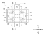
- FIG. 4A is an explanatory diagram of a current sensor according to a second embodiment of the present invention.
- FIG. 4B is a diagram showing a cross section taken along line BB' of a current sensor according to a second embodiment of the present invention.
- the basic structure of the current sensor 100A according to the second embodiment of the present invention is the same as that of the current sensor 100 according to the first embodiment, so only the differences will be explained, and the explanation of the common points will be omitted.
- the current sensor 100A according to the second embodiment is different from the current sensor 100 according to the first embodiment in the structure of the magnetic shield 30A.
- the magnetic shield 30A has a first extending portion 341, which will be described later.
- the raw material member 301A0 that provides the outermost metal plate 301A among the multilayered body made of three metal plates constituting the magnetic shield 30A is similar to the raw material members for other metal plates.
- the plate surface PS is subjected to rust prevention treatment, and has a basic shape of a rectangle that is long in one direction (X1-X2 direction), but in a direction that intersects the extending direction (X1-X2 direction) of the raw material member 301A0 (in this embodiment)
- the protruding portion 30p By bending the protruding portion 30p, as shown in FIG. 3B, the protruding portion 30p extends from the end of the base portion 31 (specifically, the bottom wall portion 33) in the first direction (Y1-Y2 direction) to the first direction.
- a first extending portion 341 extending in a perpendicular direction, in this embodiment, a third direction (Z1-Z2 direction) is formed. Therefore, the magnetic shield 30A according to the present embodiment includes the first extending portion 341 having the plate surface PS whose normal line faces in the first direction.
- the first exposed portion EP1 is constituted by the plate surface PS of the first extending portion 341.
- the first exposed portion EP1 is made of the plate surface PS that already has rust prevention properties at the stage of the raw material member 301A0, like the magnetic shield 30 of the current sensor 100 according to the first embodiment, the first exposed portion EP1 There is no need to perform any special rust prevention treatment on the exposed portion EP1.
- the side surface SS has a punched cross section and therefore does not have rust prevention properties, but even in such a case, the first embodiment Unlike the above, since the side surface SS does not constitute any exposed portion, no special anti-corrosion treatment is required.
- the first extending portion 341 is provided on the metal plate 301A forming a layer on one end side (Z2 side in the Z1-Z2 direction) in the stacking direction (third direction) of the multilayer body, and The first extending portion 341 extends toward the other end side (Z1 side in the Z1-Z2 direction) in the stacking direction (third direction) of the multilayer body.
- the portion of the metal plate 301A that constitutes the side wall portion 32 extends from the end of the base portion 31 in the second direction (X1-X2 direction) to the third direction (Z1-Z2 direction), and its normal line is in the second direction. It has a plate surface PS facing (X1-X2 direction). Therefore, when comparing the side wall portion 32 and the first extension portion 341, although the end portions of the base portion 31 from which they extend are different, they are common in that they extend in the third direction, and are oriented in a predetermined direction. They also have a plate surface PS in common.
- the side wall portion 32 can be positioned as the second extending portion.
- the metal plate 301A has a first extending portion 341 and a second extending portion (side wall portion 32). In this way, the metal plate 301A on one end side of the multilayer body has a plurality of extending portions whose normal lines face different directions, so that the ease of assembling the multilayer body may be improved.
- FIG. 5 is an explanatory diagram of a method of forming a case included in a current sensor according to a second embodiment of the present invention by insert molding, and is a top view of a magnetic shield formed by insert molding.
- FIG. 6A is an explanatory diagram of a method of forming a case included in a current sensor according to a second embodiment of the present invention by insert molding, and is a diagram showing a state in which a magnetic shield is arranged inside a molding die.
- FIG. 3 is a sectional view taken along line CC'.
- 6B is an explanatory diagram of a method of forming a case included in a current sensor according to a second embodiment of the present invention by insert molding, and is a diagram showing a state in which a magnetic shield is arranged inside a molding die. It is a sectional view taken along the line DD'.
- the magnetic shield 30A is positioned by positioning pins within the cavity formed by the upper mold 81 and lower mold 82 that constitute the molding die. Specifically, a positioning pin 931 extends from the upper mold 81 and is located above the magnetic shield 30A (Z1 side in the Z1-Z2 direction), and a positioning pin 931 extends from the lower mold 82 and is located below the magnetic shield 30A (Z1 side in the Z1-Z2 direction).
- the Z1-Z2 direction (third direction) of the magnetic shield 30A is positioned by the positioning pin 932 located on the side) contacting the plate surface PS of the magnetic shield 30A and sandwiching the bottom wall portion 33.
- the positioning pin 91 When the positioning pin 91 extending from the lower mold 82 and located in the Y1-Y2 direction of the magnetic shield 30A contacts the plate surface PS of the first extension part 341, the positioning pin 91 extends from the lower mold 82 and is positioned in the Y1-Y2 direction (first direction) of the magnetic shield 30A. is positioned.
- the positioning pins 92 extending from the upper mold 81 and located on the outside of the magnetic shield 30A in the X1-X2 direction contact the outer wall made of the plate surface PS of the side wall portion 32, thereby aligning the magnetic shield 30A in the X1-X2 direction (second direction). ) is positioned.
- the positioning pins 91 are provided on the lower mold 82 and the positioning pins 91 are provided on the upper mold 81, but the present invention is not limited thereto.
- the positioning pin 91 may be provided on the upper mold 81 and the positioning pin 91 may be provided on the lower mold 82, and both positioning pins may be provided on either the upper mold 81 or the lower mold 82. It's okay.
- the holes formed in the case after insert molding which are the marks of the positioning pins 91 and 92, have openings on the lower surface of the case. It is formed.
- the positioning pin 91 in the Y1-Y2 direction (first direction) contacts the plate surface PS of the first extension part 341, so the contact area between the positioning pin 91 and the magnetic shield 30A in the Y1-Y2 direction (first direction) can be increased. Therefore, in this embodiment, the positioning accuracy of the magnetic shield 30A inside the molding die can be higher than that in the first embodiment.
- the raw material member 301A0 that provides the metal plate 301A may have soft magnetism, or may be made of a material that does not have soft magnetism (for example, beryllium copper) with emphasis on workability.
- a molding resin is supplied into the mold (for example, by injection molding), thereby forming the case 40 in which the magnetic shield 30A is insert-molded. Ru.
- a portion of the bus bar 10 is also positioned inside the molding die, and is insert-molded together with the magnetic shield 30A.
- the insert molded member in which the magnetic shield 30A is embedded in the case 40 is an embedded member (magnetic shield 30A) obtained by punching a metal plate whose plate surface PS has rust prevention properties, and is inserted into the upper mold 81. and the lower mold 82, and is molded by supplying a resin-based material into the inside of the mold.
- the magnetic shield 30A which is an embedded member, has a plate surface PS of the first extending portion 341 as a first portion consisting of a plate surface PS facing the first direction (Y1-Y2 direction), and has a plate surface PS facing the first direction (Y1-Y2 direction). It has a plate surface PS on the outside of the side wall portion 32 as a second portion consisting of a plate surface PS facing the X1-X2 direction, and as a third portion consisting of the plate surface PS facing the third direction (Z1-Z2 direction), The bottom wall portion 33 has a plate surface PS.
- the first part of the buried member is provided in the first extension part 341, and the second part is provided in the second extension part. (the side wall portion 32), and the third portion is provided on the base portion 31, particularly the bottom wall portion 33.
- injection molding is performed inside the molding die with each of the first to third parts in contact with positioning pins 91, 92, 931, and 932 for positioning the buried member. Specifically, the first portion contacts the positioning pin 91, the second portion contacts the positioning pin 92, and the third portion contacts the positioning pins 931 and 932.
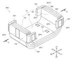
- FIG. 7 is an explanatory diagram of a magnetic shield included in a current sensor according to a third embodiment of the present invention.
- FIG. 8A is an explanatory diagram of a current sensor according to a third embodiment of the present invention.
- FIG. 8B is a diagram showing a cross section of the current sensor according to the third embodiment of the present invention, taken along line EE'.
- the current sensor 100B according to the third embodiment of the present invention has the same basic structure as the current sensor 100A according to the second embodiment, only the differences will be explained, and the explanation of the common points will be omitted.
- the current sensor 100B according to the third embodiment is different from the current sensor 100A according to the second embodiment in the structure of the magnetic shield 30B. Specifically, in the magnetic shield 30B, the extended tip portion of the first extension portion 341 is folded back so as to face the plate surface PS of the base portion 31 (bottom wall portion 33 in this embodiment). It has a protruding portion 35.
- the third exposed portion EP3 is constituted by the plate surface PS of the folded extension portion 35.
- the plate surface PS of the metal plate 303 also has rust prevention properties, but for example, the metal plate 301B that constitutes the folded extension portion 35 has a higher rust prevention property than other metal plates. If it is formed from a raw material member that has the following properties, the possibility of rusting can be more stably reduced. Moreover, if the multilayer body is caulked when forming the folded extension portion 35, the structural stability of the magnetic shield 30B can be improved.
- FIG. 9 is an explanatory diagram of a magnetic shield included in a current sensor according to a fourth embodiment of the present invention.
- the basic structure of the current sensor 100C according to the fourth embodiment of the present invention is the same as that of the current sensor 100A according to the second embodiment, so only the differences will be explained, and the explanation of the common points will be omitted.
- the shape of the metal plate 301C is different from the shape of the metal plate 301A. differ.
- the first extending portion 341 is provided on the side wall portion 32, and the first extending portion 341 is provided in the second direction among the directions orthogonal to the first direction (Y1-Y2 direction). It has a plate surface PS that extends in the (X1-X2 direction) and whose normal line faces the first direction.
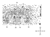
- FIG. 10A is a diagram illustrating the shielding effect of the magnetic shield included in the current sensor according to the fourth embodiment of the present invention, and is a cross section taken along the line F-F' in FIG. 9.
- FIG. 10B is a diagram illustrating the shielding effect of the magnetic shield included in the current sensor according to the fourth embodiment of the present invention, and is a diagram (top view) of the current sensor 100 viewed from the Z1 side in the Z1-Z2 direction.
- the substrate 50 and the lid part 60 are not shown.
- the bus bar 10 is replaced with a current line 10i.
- simulation results of the strength and direction of the induced magnetic field due to the current flowing through the current line 10i are shown by a plurality of arrowhead-shaped marks.
- FIG. 11A is a diagram (cross-sectional view) illustrating the shielding effect of the magnetic shield included in the current sensor according to the first embodiment of the present invention.
- FIG. 11B is a diagram (top view) illustrating the shielding effect of the magnetic shield included in the current sensor according to the first embodiment of the present invention.
- FIGS. 11A and 11B are shown in contrast with FIGS. 10A and 10B.
- the induced magnetic field generated by the current flowing through the bus bar 10 is A magnetic field is emitted from the end of the side wall portion 32 through the shield 30), and efficient application of the magnetic field to the magnetic sensor 20 is realized.
- the fourth embodiment since the magnetic field preferentially flows through the first extension part 341, the strong magnetic field is applied not only to the side wall part 32 but also to the first extension part 341. It is also released from the outlet 341.
- the magnetic field is preferentially emitted only from the side wall portion 32. Therefore, when comparing the magnetic flux density of the magnetic field applied to the magnetic sensor 20, the fourth embodiment has a higher magnetic flux density than the first embodiment.
- the magnetic field strength applied to the magnetic sensor 20 is at most 35 mT or less, but in FIG. 11 showing the fourth embodiment, the magnetic field strength applied to the magnetic sensor 20 is The magnetic field strength reaches a maximum of 45 mT. In this way, since the magnetic field from the bus bar 10 located inside the magnetic shield 30C is strongly applied, the influence of the external magnetic field is relatively reduced. Therefore, the fourth embodiment has higher detection sensitivity than the first embodiment and is less susceptible to external magnetic fields. According to this simulation, the adjacent influence error in the configuration of the first embodiment is 2.2%, but in the case of the configuration of the fourth embodiment, the adjacent influence error is reduced to 1.6%.
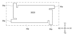
- FIG. 12A is an explanatory diagram of a raw material member of a magnetic shield included in a current sensor according to a fifth embodiment of the present invention.
- FIG. 12B is a top view (view from the Z1 side in the Z1-Z2 direction) of the magnetic shield included in the current sensor according to the fifth embodiment of the present invention.
- FIG. 12C is a side view (view from the Y2 side in the Y1-Y2 direction) of the magnetic shield included in the current sensor according to the fifth embodiment of the present invention.
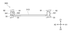
- the current sensor according to the fifth embodiment of the present invention has a structure as shown in Patent Document 1, for example, and the basic shape of the base 31D of the magnetic shield 30D is a flat plate shape. As shown, it has a first extending part 341 and a second extending part 342.
- the magnetic shield 30D is formed from a raw material member 30D0 as shown in FIG. 12A.
- the raw material member 30D0 is obtained by, for example, punching the raw metal plate PM.
- the raw material member 30D0 has a protrusion 30p extending in the X1-X2 direction (second direction) or the Y1-Y2 direction (first direction). By individually bending these protruding parts 30p in the Z1-Z2 direction Z1 side, the base 31D, the first extending part 341, and the second extending part 342 are formed as shown in FIGS. 12B and 12C.
- a magnetic shield 30D having the following properties is obtained.
- the magnetic shield 30D placed inside the molding die for insert molding contacts the positioning pin 91 in the Y1-Y2 direction (first direction) on the plate surface PS of the first extension part 341, and The projecting portion 342 comes into contact with the positioning pin 92 in the X1-X2 direction (second direction).
- the magnetic shield 30D contacts a positioning pin in the Z1-Z2 direction (second direction) on the plate surface PS of the base 31D. In this way, by contacting the positioning pins (positioning pin 91, positioning pin 92) with the extension parts (first extension part 341, second extension part 342), positioning can be performed regardless of the thickness of the metal plate.
- the folded extension portion 35 is folded back so as to face the plate surface PS of the metal plate 303 that is different from the metal plate 301B having the folded extension portion 35, but the folded extension portion 35 is not limited thereto.
- the metal plate 301B having the folded extension portion 35 may be folded so as to face the plate surface PS.
- the position where the folded extension portion 35 is provided is not limited either.
- the folded extension portion 35 may be provided in any of the first portion, second portion, and third portion of the buried member (magnetic shield), or may be provided in a plurality of different portions.
Landscapes
- Physics & Mathematics (AREA)
- General Physics & Mathematics (AREA)
- Engineering & Computer Science (AREA)
- Power Engineering (AREA)
- Measuring Instrument Details And Bridges, And Automatic Balancing Devices (AREA)
Priority Applications (2)
| Application Number | Priority Date | Filing Date | Title |
|---|---|---|---|
| JP2024511326A JPWO2023188787A1 (https=) | 2022-03-30 | 2023-01-31 | |
| US18/770,062 US20240361358A1 (en) | 2022-03-30 | 2024-07-11 | Current sensor and method of manufacturing insert-molded component |
Applications Claiming Priority (2)
| Application Number | Priority Date | Filing Date | Title |
|---|---|---|---|
| JP2022055196 | 2022-03-30 | ||
| JP2022-055196 | 2022-03-30 |
Related Child Applications (1)
| Application Number | Title | Priority Date | Filing Date |
|---|---|---|---|
| US18/770,062 Continuation US20240361358A1 (en) | 2022-03-30 | 2024-07-11 | Current sensor and method of manufacturing insert-molded component |
Publications (1)
| Publication Number | Publication Date |
|---|---|
| WO2023188787A1 true WO2023188787A1 (ja) | 2023-10-05 |
Family
ID=88200816
Family Applications (1)
| Application Number | Title | Priority Date | Filing Date |
|---|---|---|---|
| PCT/JP2023/003082 Ceased WO2023188787A1 (ja) | 2022-03-30 | 2023-01-31 | 電流センサおよびインサート成形部材の製造方法 |
Country Status (3)
| Country | Link |
|---|---|
| US (1) | US20240361358A1 (https=) |
| JP (1) | JPWO2023188787A1 (https=) |
| WO (1) | WO2023188787A1 (https=) |
Cited By (1)
| Publication number | Priority date | Publication date | Assignee | Title |
|---|---|---|---|---|
| WO2025074794A1 (ja) * | 2023-10-03 | 2025-04-10 | アルプスアルパイン株式会社 | 電流センサおよび電流センサの製造方法 |
Citations (8)
| Publication number | Priority date | Publication date | Assignee | Title |
|---|---|---|---|---|
| JPH0686080U (ja) * | 1993-05-21 | 1994-12-13 | スタンレー電気株式会社 | 電流検出装置 |
| JP2012247219A (ja) * | 2011-05-25 | 2012-12-13 | Glory Ltd | 磁気センサ用磁石アレイの製造方法及び磁気センサの製造方法 |
| JP2016031293A (ja) * | 2014-07-29 | 2016-03-07 | 株式会社東海理化電機製作所 | 磁気シールド及びその製造方法 |
| JP2017102022A (ja) * | 2015-12-02 | 2017-06-08 | アルプス電気株式会社 | 電流センサ |
| JP2018119994A (ja) * | 2015-02-02 | 2018-08-02 | 株式会社村田製作所 | 電流センサ |
| US20200267841A1 (en) * | 2019-02-15 | 2020-08-20 | Lg Electronics Inc. | Printed circuit board assembly |
| JP2021036200A (ja) * | 2017-12-13 | 2021-03-04 | アルプスアルパイン株式会社 | 電流センサ及び電流センサのケースの製造方法 |
| WO2022024610A1 (ja) * | 2020-07-28 | 2022-02-03 | アルプスアルパイン株式会社 | 電流センサ |
Family Cites Families (4)
| Publication number | Priority date | Publication date | Assignee | Title |
|---|---|---|---|---|
| US6956307B2 (en) * | 2004-03-08 | 2005-10-18 | Amsted Industries Incorporated | Soft magnetic composite powder metal cores |
| JP2009083742A (ja) * | 2007-10-01 | 2009-04-23 | Nishikawa Rubber Co Ltd | インサートパネル埋設ウェザーストリップおよびその製造方法 |
| US8317319B2 (en) * | 2010-09-24 | 2012-11-27 | Karl Hellberg | Co-axial multi-tip eyeglass retainer coupling and method of use |
| JP5900402B2 (ja) * | 2013-04-01 | 2016-04-06 | 株式会社デンソー | 電流センサ用の磁気シールド体 |
-
2023
- 2023-01-31 JP JP2024511326A patent/JPWO2023188787A1/ja active Pending
- 2023-01-31 WO PCT/JP2023/003082 patent/WO2023188787A1/ja not_active Ceased
-
2024
- 2024-07-11 US US18/770,062 patent/US20240361358A1/en active Pending
Patent Citations (8)
| Publication number | Priority date | Publication date | Assignee | Title |
|---|---|---|---|---|
| JPH0686080U (ja) * | 1993-05-21 | 1994-12-13 | スタンレー電気株式会社 | 電流検出装置 |
| JP2012247219A (ja) * | 2011-05-25 | 2012-12-13 | Glory Ltd | 磁気センサ用磁石アレイの製造方法及び磁気センサの製造方法 |
| JP2016031293A (ja) * | 2014-07-29 | 2016-03-07 | 株式会社東海理化電機製作所 | 磁気シールド及びその製造方法 |
| JP2018119994A (ja) * | 2015-02-02 | 2018-08-02 | 株式会社村田製作所 | 電流センサ |
| JP2017102022A (ja) * | 2015-12-02 | 2017-06-08 | アルプス電気株式会社 | 電流センサ |
| JP2021036200A (ja) * | 2017-12-13 | 2021-03-04 | アルプスアルパイン株式会社 | 電流センサ及び電流センサのケースの製造方法 |
| US20200267841A1 (en) * | 2019-02-15 | 2020-08-20 | Lg Electronics Inc. | Printed circuit board assembly |
| WO2022024610A1 (ja) * | 2020-07-28 | 2022-02-03 | アルプスアルパイン株式会社 | 電流センサ |
Cited By (1)
| Publication number | Priority date | Publication date | Assignee | Title |
|---|---|---|---|---|
| WO2025074794A1 (ja) * | 2023-10-03 | 2025-04-10 | アルプスアルパイン株式会社 | 電流センサおよび電流センサの製造方法 |
Also Published As
| Publication number | Publication date |
|---|---|
| JPWO2023188787A1 (https=) | 2023-10-05 |
| US20240361358A1 (en) | 2024-10-31 |
Similar Documents
| Publication | Publication Date | Title |
|---|---|---|
| US9366733B2 (en) | Sensor package and method for producing a sensor package having alignment marks or structures | |
| KR20110057262A (ko) | 프린트 배선판 및 그 제조 방법 | |
| JP5817508B2 (ja) | 電流検出装置 | |
| WO2023188787A1 (ja) | 電流センサおよびインサート成形部材の製造方法 | |
| CN1885451B (zh) | 线圈部件 | |
| US20210193369A1 (en) | Coil component | |
| US10453601B2 (en) | Coil device | |
| US7877867B2 (en) | Component fixing method | |
| JP7452398B2 (ja) | 電流センサ | |
| JP5099271B2 (ja) | 電流センサ及び電流センサの製造方法 | |
| US20240212919A1 (en) | Coil device | |
| JP5703518B2 (ja) | 電流センサ | |
| JP5083135B2 (ja) | 電流センサ及び電流センサの製造方法 | |
| KR20220099006A (ko) | 코일 부품 | |
| JP2006071456A (ja) | 電流計測装置 | |
| US20240339262A1 (en) | Magnetic component | |
| JP2013131549A (ja) | 部品実装ずれ判定方法 | |
| US20250123311A1 (en) | Quantifiable electromagnetic relay and electronic energy meter | |
| JP2009064911A (ja) | 電子回路モジュール | |
| JP2010129917A (ja) | コイル部品 | |
| US20230317351A1 (en) | Electronic component | |
| EP4734287A1 (en) | Antenna module | |
| JP2007173576A (ja) | コイル部品及びコイル部品の製造方法 | |
| JP2014098634A (ja) | 電流センサ | |
| JP5671276B2 (ja) | 小型モータ |
Legal Events
| Date | Code | Title | Description |
|---|---|---|---|
| 121 | Ep: the epo has been informed by wipo that ep was designated in this application |
Ref document number: 23776833 Country of ref document: EP Kind code of ref document: A1 |
|
| WWE | Wipo information: entry into national phase |
Ref document number: 2024511326 Country of ref document: JP |
|
| NENP | Non-entry into the national phase |
Ref country code: DE |
|
| 122 | Ep: pct application non-entry in european phase |
Ref document number: 23776833 Country of ref document: EP Kind code of ref document: A1 |