WO2023181587A1 - ジャンクションバリアショットキーダイオード - Google Patents
ジャンクションバリアショットキーダイオード Download PDFInfo
- Publication number
- WO2023181587A1 WO2023181587A1 PCT/JP2023/000365 JP2023000365W WO2023181587A1 WO 2023181587 A1 WO2023181587 A1 WO 2023181587A1 JP 2023000365 W JP2023000365 W JP 2023000365W WO 2023181587 A1 WO2023181587 A1 WO 2023181587A1
- Authority
- WO
- WIPO (PCT)
- Prior art keywords
- type semiconductor
- semiconductor layer
- layer
- schottky diode
- valence band
- Prior art date
- Legal status (The legal status is an assumption and is not a legal conclusion. Google has not performed a legal analysis and makes no representation as to the accuracy of the status listed.)
- Ceased
Links
Images






Classifications
-
- H—ELECTRICITY
- H10—SEMICONDUCTOR DEVICES; ELECTRIC SOLID-STATE DEVICES NOT OTHERWISE PROVIDED FOR
- H10D—INORGANIC ELECTRIC SEMICONDUCTOR DEVICES
- H10D8/00—Diodes
- H10D8/60—Schottky-barrier diodes
-
- H—ELECTRICITY
- H10—SEMICONDUCTOR DEVICES; ELECTRIC SOLID-STATE DEVICES NOT OTHERWISE PROVIDED FOR
- H10D—INORGANIC ELECTRIC SEMICONDUCTOR DEVICES
- H10D62/00—Semiconductor bodies, or regions thereof, of devices having potential barriers
- H10D62/80—Semiconductor bodies, or regions thereof, of devices having potential barriers characterised by the materials
- H10D62/82—Heterojunctions
-
- H—ELECTRICITY
- H10—SEMICONDUCTOR DEVICES; ELECTRIC SOLID-STATE DEVICES NOT OTHERWISE PROVIDED FOR
- H10D—INORGANIC ELECTRIC SEMICONDUCTOR DEVICES
- H10D62/00—Semiconductor bodies, or regions thereof, of devices having potential barriers
- H10D62/10—Shapes, relative sizes or dispositions of the regions of the semiconductor bodies; Shapes of the semiconductor bodies
- H10D62/102—Constructional design considerations for preventing surface leakage or controlling electric field concentration
- H10D62/103—Constructional design considerations for preventing surface leakage or controlling electric field concentration for increasing or controlling the breakdown voltage of reverse-biased devices
- H10D62/105—Constructional design considerations for preventing surface leakage or controlling electric field concentration for increasing or controlling the breakdown voltage of reverse-biased devices by having particular doping profiles, shapes or arrangements of PN junctions; by having supplementary regions, e.g. junction termination extension [JTE]
- H10D62/106—Constructional design considerations for preventing surface leakage or controlling electric field concentration for increasing or controlling the breakdown voltage of reverse-biased devices by having particular doping profiles, shapes or arrangements of PN junctions; by having supplementary regions, e.g. junction termination extension [JTE] having supplementary regions doped oppositely to or in rectifying contact with regions of the semiconductor bodies, e.g. guard rings with PN or Schottky junctions
-
- H—ELECTRICITY
- H10—SEMICONDUCTOR DEVICES; ELECTRIC SOLID-STATE DEVICES NOT OTHERWISE PROVIDED FOR
- H10D—INORGANIC ELECTRIC SEMICONDUCTOR DEVICES
- H10D62/00—Semiconductor bodies, or regions thereof, of devices having potential barriers
- H10D62/10—Shapes, relative sizes or dispositions of the regions of the semiconductor bodies; Shapes of the semiconductor bodies
- H10D62/117—Shapes of semiconductor bodies
-
- H—ELECTRICITY
- H10—SEMICONDUCTOR DEVICES; ELECTRIC SOLID-STATE DEVICES NOT OTHERWISE PROVIDED FOR
- H10D—INORGANIC ELECTRIC SEMICONDUCTOR DEVICES
- H10D62/00—Semiconductor bodies, or regions thereof, of devices having potential barriers
- H10D62/10—Shapes, relative sizes or dispositions of the regions of the semiconductor bodies; Shapes of the semiconductor bodies
- H10D62/124—Shapes, relative sizes or dispositions of the regions of semiconductor bodies or of junctions between the regions
- H10D62/126—Top-view geometrical layouts of the regions or the junctions
-
- H—ELECTRICITY
- H10—SEMICONDUCTOR DEVICES; ELECTRIC SOLID-STATE DEVICES NOT OTHERWISE PROVIDED FOR
- H10D—INORGANIC ELECTRIC SEMICONDUCTOR DEVICES
- H10D62/00—Semiconductor bodies, or regions thereof, of devices having potential barriers
- H10D62/80—Semiconductor bodies, or regions thereof, of devices having potential barriers characterised by the materials
- H10D62/875—Semiconductor bodies, or regions thereof, of devices having potential barriers characterised by the materials being semiconductor metal oxide, e.g. InGaZnO
Definitions
- the present invention relates to a junction barrier Schottky diode, and particularly to a junction barrier Schottky diode using gallium oxide.
- a Schottky barrier diode is a rectifying element that utilizes the Schottky barrier created by the junction of a metal and a semiconductor, and has the characteristics of a lower forward voltage and faster switching speed than a normal diode with a PN junction. are doing. For this reason, Schottky barrier diodes are sometimes used as switching elements for power devices.
- gallium oxide has a very large band gap of 4.8 to 4.9 eV and a large dielectric breakdown field of about 8 MV/cm, so Schottky barrier diodes using gallium oxide are suitable for switching power devices. It is very promising as a device.
- An example of a Schottky barrier diode using gallium oxide is described in Patent Document 1.
- Patent Document 1 discloses a junction barrier Schottky diode having a structure in which a p-type semiconductor material is embedded in a plurality of trenches provided in a gallium oxide layer. In this way, if a plurality of trenches are provided in the gallium oxide layer and a p-type semiconductor material is buried in the plurality of trenches, the mesa region located between the trenches becomes a depletion layer when a reverse voltage is applied. The channel region of the drift layer is pinched off. This makes it possible to significantly suppress leakage current when a reverse voltage is applied.
- the present invention aims to increase the surge resistance of a junction barrier Schottky diode using gallium oxide.
- a junction barrier Schottky diode includes a semiconductor substrate made of gallium oxide, a drift layer made of gallium oxide provided on the semiconductor substrate, an anode electrode in contact with the drift layer, a cathode electrode in contact with the semiconductor substrate, and an anode.
- the top level of the valence band of the p-type semiconductor layer is lower than the top level of the valence band of the first p-type semiconductor layer.
- the difference between the Fermi level and the top level of the valence band of the p-type semiconductor layer can be reduced, and the difference between the Fermi level and the top level of the valence band of the p-type semiconductor layer can be reduced. It becomes possible to reduce the difference between the upper end level of the valence band and the upper end level of the valence band of the drift layer.
- the second p-type semiconductor layer and the first p-type semiconductor layer may be stacked in this order on the flat upper surface of the drift layer. According to this, it becomes possible to produce with a simple manufacturing process.
- the drift layer may have a trench, and at least a portion of the p-type semiconductor layer may be buried in the trench. According to this, it becomes possible to expand the contact area between the p-type semiconductor layer and the drift layer.
- the energy difference between the Fermi level and the valence band top level of the first p-type semiconductor layer is 1 eV or less
- the energy difference between the valence band top level of the second p-type semiconductor layer and the valence band level of the drift layer is 1 eV or less
- the energy difference between the band top levels may be 2 eV or less. According to this, it is possible to bring the anode electrode and the first p-type semiconductor layer into ohmic contact, and it is also possible to sufficiently reduce the energy required to inject holes into the drift layer.
- the p-type semiconductor layer further includes a third p-type semiconductor layer located between the first p-type semiconductor layer and the second p-type semiconductor layer, and the value of the third p-type semiconductor layer is
- the electron band top level may be lower than the valence band top level of the first p-type semiconductor layer and higher than the valence band top level of the second p-type semiconductor layer. According to this, it becomes possible to further increase surge resistance.
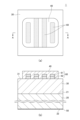
- FIG. 1(a) is a schematic plan view showing the configuration of a junction barrier Schottky diode 1 according to a first embodiment of the present invention. Further, FIG. 1(b) is a schematic cross-sectional view taken along the line AA shown in FIG. 1(a).
- FIG. 2 is an energy band diagram of the junction barrier Schottky diode 1, in which (a) shows the energy band in the first current path P1, and (b) shows the energy band in the second current path P2. .
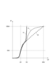
- FIG. 3 is a graph showing the relationship between forward voltage VF and forward current IF.
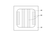
- FIG. 4 is a schematic plan view showing the structure of a junction barrier Schottky diode according to a first modification.
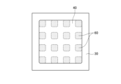
- FIG. 5 is a schematic plan view showing the configuration of a junction barrier Schottky diode according to a second modification.
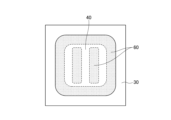
- FIG. 6 is a schematic plan view showing the structure of a junction barrier Schottky diode according to a third modification.
- FIG. 7 is a schematic plan view showing the configuration of a junction barrier Schottky diode according to a fourth modification.
- FIG. 8A is a schematic plan view showing the configuration of a junction barrier Schottky diode according to a fifth modification. Further, FIG. 8(b) is a schematic cross-sectional view taken along the line AA shown in FIG. 8(a).
- FIG. 9A is a schematic plan view showing the configuration of a junction barrier Schottky diode according to a sixth modification. Further, FIG.
- FIG. 9(b) is a schematic cross-sectional view taken along the line AA shown in FIG. 9(a).
- FIG. 10A is a schematic plan view showing the configuration of a junction barrier Schottky diode according to a seventh modification.
- FIG. 10(b) is a schematic cross-sectional view taken along the line AA shown in FIG. 10(a).
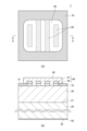
- FIG. 11(a) is a schematic plan view showing the configuration of a junction barrier Schottky diode 2 according to the second embodiment of the present invention.
- FIG. 11(b) is a schematic cross-sectional view taken along the line AA shown in FIG. 11(a).
- FIG. 12 is a schematic cross-sectional view showing the structure of a junction barrier Schottky diode according to an eighth modification.
- FIG. 13 is a schematic cross-sectional view showing the structure of a junction barrier Schottky diode 3 according to the third embodiment of the present invention.
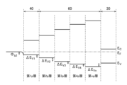
- FIG. 14 is an energy band diagram of the junction barrier Schottky diode 3, showing the energy band in the second current path P2.
- FIG. 15 is an energy band diagram according to a first example when the p-type semiconductor layer 60 has an n-layer structure.
- FIG. 16 is an energy band diagram according to a second example in which the p-type semiconductor layer 60 has an n-layer structure.
- FIG. 1(a) is a schematic plan view showing the configuration of a junction barrier Schottky diode 1 according to a first embodiment of the present invention. Further, FIG. 1(b) is a schematic cross-sectional view taken along the line AA shown in FIG. 1(a).
- the junction barrier Schottky diode 1 includes a semiconductor substrate 20 and a drift layer 30, both of which are made of gallium oxide ( ⁇ -Ga 2 O 3 ). Silicon (Si) or tin (Sn) is introduced into the semiconductor substrate 20 and the drift layer 30 as an n-type dopant.
- the dopant concentration is higher in the semiconductor substrate 20 than in the drift layer 30, so that the semiconductor substrate 20 functions as an n + layer and the drift layer 30 functions as an n ⁇ layer.
- the impurity concentration of the semiconductor substrate 20 is, for example, about 1 ⁇ 10 18 cm ⁇ 3
- the impurity concentration of the drift layer 30 is, for example, about 3 ⁇ 10 16 cm ⁇ 3 .
- the semiconductor substrate 20 is obtained by cutting a bulk crystal formed using a melt growth method or the like, and has a thickness of about 250 ⁇ m.
- the planar size of the semiconductor substrate 20 is not particularly limited, but it is generally selected depending on the amount of current flowing through the element. If the maximum amount of current in the forward direction is about 20A, the planar size of the semiconductor substrate 20 is 2.4mm ⁇ 2.4mm in plan view. It may be approximately 2.4 mm.
- the semiconductor substrate 20 has an upper surface 21 located on the upper surface side during mounting, and a back surface 22 opposite to the upper surface 21 and located on the lower surface side during mounting.
- a drift layer 30 is formed over the entire top surface 21 .
- the drift layer 30 is a thin film formed by epitaxially growing gallium oxide on the upper surface 21 of the semiconductor substrate 20 using reactive sputtering, PLD, MBE, MOCVD, HVPE, or the like.
- the film thickness of the drift layer 30 is not particularly limited, it is generally selected depending on the reverse dielectric strength of the element, and in order to ensure a dielectric strength of approximately 600V, it may be set to, for example, approximately 7 ⁇ m.
- an anode electrode 40 that makes Schottky contact with the drift layer 30 and a p-type semiconductor layer 60 that makes a pn junction with the drift layer 30 are formed.
- the anode electrode 40 is made of metal such as platinum (Pt), palladium (Pd), gold (Au), nickel (Ni), molybdenum (Mo), and copper (Cu).
- the anode electrode 40 may have a multilayer structure in which different metal films are laminated, for example, Pt/Au, Pt/Al, Pd/Au, Pd/Al, Pt/Ti/Au, or Pd/Ti/Au.
- the p-type semiconductor layer 60 includes a first p-type semiconductor layer 61 and a second p-type semiconductor layer 62.
- the p-type semiconductor layer 60 is formed in a double ring shape in plan view, and a second p-type semiconductor layer 62 and a first p-type semiconductor layer 61 are laminated in this order on the flat upper surface 31 of the drift layer 30. has been done.
- the first p-type semiconductor layer 61 comes into contact with the anode electrode 40
- the second p-type semiconductor layer 62 forms a pn junction with the drift layer 30.
- the side surface of the second p-type semiconductor layer 62 is also in contact with the anode electrode 40.
- the materials for the first and second p-type semiconductor layers 61 and 62 include Si, GaAs, GaN, SiC, Ge, ZnSe, CdS, InP, SiGe, AlN, BN, AlGaN, NiO, Cu2O , and Ir2.
- O 3 , Ag 2 O, etc. can be used, but at least as a material for the second p-type semiconductor layer 62, the upper end level of the valence band is equal to the upper end level of the valence band of the first p-type semiconductor layer 61. It is necessary to select a material with a lower temperature.
- NiO with an impurity concentration of about 1 ⁇ 10 19 cm ⁇ 3 can be selected as the first p-type semiconductor layer 61, and NiO with an impurity concentration of about 1 ⁇ 10 16 as the second p-type semiconductor layer 62.
- a BN of about cm ⁇ 3 can be selected.
- a cathode electrode 50 that makes ohmic contact with the semiconductor substrate 20 is provided on the back surface 22 of the semiconductor substrate 20 .
- the cathode electrode 50 is made of metal such as titanium (Ti), for example.
- the cathode electrode 50 may have a multilayer structure in which different metal films are laminated, for example, Ti/Au or Ti/Al.
- the first current path is a path through which current flows directly from the anode electrode 40 to the drift layer 30 without passing through the p-type semiconductor layer 60, as indicated by the symbol P1 in FIG. 1(b).
- the second current path is a path passing through the p-type semiconductor layer 60, as indicated by the symbol P2 in FIG. 1(b).
- FIG. 2 is an energy band diagram of the junction barrier Schottky diode 1 according to the present embodiment, in which (a) shows the energy band in the first current path P1, and (b) shows the energy band in the second current path P2. It shows.
- E F means the Fermi level
- E C means the lower end level of the conduction band
- E V means the upper end level of the valence band
- E g means the energy band gap.
- the p-type semiconductor layer 60 is interposed between the anode electrode 40 and the drift layer 30. Therefore, after a current flows through the first current path P1, when a higher forward voltage is applied, the second current path P2 is turned on. This significantly reduces on-resistance.
- FIG. 3 is a graph showing the relationship between forward voltage VF and forward current IF, where symbol A indicates the characteristics of the junction barrier Schottky diode 1 according to this embodiment, and symbol B indicates the characteristic of the general Schottky barrier diode. It shows the characteristics.
- A indicates the characteristics of the junction barrier Schottky diode 1 according to this embodiment
- symbol B indicates the characteristic of the general Schottky barrier diode. It shows the characteristics.
- FIG. 3 shows that in a typical Schottky barrier diode, when a sudden large current (surge current) of, for example, 100 A flows, a voltage of about 50 V is generated, and the diode burns out due to a large amount of heat generated.
- the second current path P2 is turned on, so the generated voltage is suppressed to about 5V. It will be done.
- the first p-type semiconductor layer 61 and the second p-type semiconductor layer 62 are arranged in this order between the anode electrode 40 and the drift layer 30.
- the energy difference between the Fermi level E F and the top level of the valence band of the first p-type semiconductor layer 61 is ⁇ b2
- the energy difference between the level and the top level of the valence band of the second p-type semiconductor layer 62 is ⁇ E V1
- the difference between the top level of the valence band of the second p-type semiconductor layer 62 and the top level of the valence band of the drift layer 30 is ⁇ E V1
- the energy difference between the positions is ⁇ E V2 .
- the band gap of the first p-type semiconductor layer 61 is E g1
- the band gap of the second p-type semiconductor layer 62 is E g2
- the band gap of the drift layer 30 is E g3 .
- the p-type semiconductor layer 60 The energy differences ⁇ b2 and ⁇ E V2 are reduced compared to the case where a single semiconductor material is used as the material. As a result, the energy required to inject holes into the drift layer 30 is reduced, and the contact resistance between the anode electrode 40 and the p-type semiconductor layer 60 is reduced. The surge resistance is increased compared to the case where the same semiconductor material is used.
- the materials for the first and second p-type semiconductor layers 61 and 62 it is preferable to select materials such that the energy difference ⁇ b2 is 1 eV or less and the energy difference ⁇ E V2 is 2 eV or less.
- the band gap E g1 of NiO is about 3.7 eV
- the band gap of BN is about 3.7 eV
- E g2 is about 6.2 eV
- the energy difference ⁇ b2 is 0.5 eV or less.
- the energy difference ⁇ E V2 is also 2 eV or less, and the energy required to inject holes into the drift layer 30 is sufficiently reduced.
- NiO is used as the material of the first p-type semiconductor layer 61 and AlN is used as the material of the second p-type semiconductor layer 62.
- Cu 2 O as the material of the first p-type semiconductor layer 61 and AlN as the material of the second p-type semiconductor layer 62
- GaN as the material of the first p-type semiconductor layer 61 and BN
- AlGaN may be used as the material of the first p-type semiconductor layer 61
- BN may be used as the material of the second p-type semiconductor layer 62
- BN may be used as the material of the first p-type semiconductor layer 62.
- CuGaO 2 may be used as the material for the p-type semiconductor layer 61
- BN may be used as the material for the second p-type semiconductor layer 62.
- the junction barrier Schottky diode 1 has a p-type semiconductor layer 60 formed of a stacked body of the first and second p-type semiconductor layers 61 and 62. Compared to the case where a single semiconductor material is used as the material of 60, it is possible to obtain a larger surge resistance. Moreover, since the p-type semiconductor layer 60 is formed on the flat upper surface 31 of the drift layer 30, it can be manufactured using a simple manufacturing process.
- the planar shape of the p-type semiconductor layer 60 is not limited to the shape shown in FIG. It may be dot-like as in the second modification example shown in FIG. 5, it may be a combination of rings and stripes as in the third modification example shown in FIG. It is also possible to use a combination of rings and dots as in the modified example. Further, a part of the p-type semiconductor layer 60 does not need to be covered with the anode electrode 40 as in the fifth modification shown in FIG. 8, or as in the sixth modification shown in FIG. The width of the p-type semiconductor layer 60 may be larger than that of the p-type semiconductor layer 60. Furthermore, as in a seventh modification shown in FIG.
- a field insulating film 70 may be provided on the upper surface 31 of the drift layer 30, and the end portion of the anode electrode 40 may be disposed on the field insulating film 70.
- FIG. 11(a) is a schematic plan view showing the configuration of a junction barrier Schottky diode 2 according to the second embodiment of the present invention. Further, FIG. 11(b) is a schematic cross-sectional view taken along the line AA shown in FIG. 11(a).
- the junction barrier Schottky diode 2 according to the second embodiment has a trench 32 provided in the drift layer 30, and a second p-type semiconductor layer 62 embedded in the trench 32. This is different from the junction barrier Schottky diode 1 according to the first embodiment.
- Other basic configurations are the same as the junction barrier Schottky diode 1 according to the first embodiment, so the same elements are denoted by the same reference numerals and redundant explanation will be omitted.
- the trench 32 has a depth that does not reach the semiconductor substrate 20 from the top surface 31 of the drift layer 30, and the second p-type semiconductor layer 62 is buried inside the trench 32.
- the depth of the trench 32 can be about 3 ⁇ m, and the width of the trench 32 can be about 1.5 ⁇ m.
- the first p-type semiconductor layer 61 is provided at a position outside the trench 32 and in contact with the second p-type semiconductor layer 62 . Therefore, in this embodiment, the anode electrode 40 and the second p-type semiconductor layer 62 are not in direct contact.
- the second p-type semiconductor layer 62 is embedded in the trench 32 provided in the drift layer 30, the second p-type semiconductor layer 62 is buried in the trench 32 provided in the drift layer 30.
- the contact area between the semiconductor layer 62 and the drift layer 30 increases. This makes it possible to further reduce the resistance value of the second current path P2.
- the entire second p-type semiconductor layer 62 is buried in the trench 32, but a part of the second p-type semiconductor layer 62 is provided outside the trench 32.
- the entire p-type semiconductor layer 60 including the first p-type semiconductor layer 61 may be buried in the trench 32 as in the modification shown in FIG.
- FIG. 13 is a schematic cross-sectional view showing the structure of a junction barrier Schottky diode 3 according to the third embodiment of the present invention.
- the junction barrier Schottky diode 3 according to the third embodiment is different from the junction barrier diode according to the first embodiment in that the p-type semiconductor layer 60 includes a third p-type semiconductor layer 63. This is different from the barrier Schottky diode 1.
- Other basic configurations are the same as the junction barrier Schottky diode 1 according to the first embodiment, so the same elements are denoted by the same reference numerals and redundant explanation will be omitted.
- the third p-type semiconductor layer 63 is located between the first p-type semiconductor layer 61 and the second p-type semiconductor layer 62.
- the material for the third p-type semiconductor layer 63 has a valence band upper level lower than the valence band upper level of the first p-type semiconductor layer 61, and a material for the second p-type semiconductor layer 63.
- a material having a higher valence band upper level than 62 is selected.
- FIG. 14 is an energy band diagram of the junction barrier Schottky diode 3 according to this embodiment, and shows the energy band in the second current path P2.
- the Fermi level E F and the upper valence band level of the first p-type semiconductor layer 61 The energy difference ⁇ b2 and the energy difference ⁇ E V2 between the valence band upper end level of the second p-type semiconductor layer 62 and the valence band upper end level of the drift layer 30 can be further reduced.
- the energy required to inject holes into the drift layer 30 is further reduced, and the contact resistance between the anode electrode 40 and the p-type semiconductor layer 60 is further reduced, so that surge resistance can be further increased. becomes possible.
- the p-type semiconductor layer 60 has a three-layer structure, it is possible to further increase the surge resistance. Furthermore, it is also possible to form the p-type semiconductor layer 60 into a layered structure of four or more layers. For example, when the p-type semiconductor layer has an n-layer structure, as shown in FIG. 15, the p-type semiconductor layer located on the anode electrode 40 side (the fourth p-type semiconductor layer in FIG. There may be some combinations in which the top level of the valence band of the layer) is lower than the top level of the valence band of the p-type semiconductor layer (np layer in FIG. 15) located on the drift layer 30 side.
- the upper end level of the valence band of the p-type semiconductor layer (np layer in FIG. 15) located closest to the drift layer 30 is lower than the upper end level of the valence band of the drift layer 30. I don't mind.
Landscapes
- Electrodes Of Semiconductors (AREA)
Abstract
Description
図1(a)は、本発明の第1の実施形態によるジャンクションバリアショットキーダイオード1の構成を示す模式的な平面図である。また、図1(b)は、図1(a)に示すA-A線に沿った略断面図である。
図11(a)は、本発明の第2の実施形態によるジャンクションバリアショットキーダイオード2の構成を示す模式的な平面図である。また、図11(b)は、図11(a)に示すA-A線に沿った略断面図である。
図13は、本発明の第3の実施形態によるジャンクションバリアショットキーダイオード3の構成を示す模式的な断面図である。
20 半導体基板
21 半導体基板の上面
22 半導体基板の裏面
30 ドリフト層
31 半導体基板の上面
32 トレンチ
40 アノード電極
50 カソード電極
60 p型半導体層
61 第1のp型半導体層
62 第2のp型半導体層
63 第3のp型半導体層
70 フィールド絶縁膜
P1 第1の電流パス
P2 第2の電流パス
Claims (5)
- 酸化ガリウムからなる半導体基板と、
前記半導体基板上に設けられた酸化ガリウムからなるドリフト層と、
前記ドリフト層と接するアノード電極と、
前記半導体基板と接するカソード電極と、
前記アノード電極及びドリフト層と接するp型半導体層と、を備え、
前記p型半導体層は、前記アノード電極と接する第1のp型半導体層と、前記ドリフト層と接する第2のp型半導体層とを含み、
前記第2のp型半導体層の価電子帯上端準位は、前記第1のp型半導体層の価電子帯上端準位よりも低いことを特徴とするジャンクションバリアショットキーダイオード。 - 前記第2のp型半導体層と前記第1のp型半導体層は、前記ドリフト層の平坦な上面にこの順に積層されていることを特徴とする請求項1に記載のジャンクションバリアショットキーダイオード。
- 前記ドリフト層はトレンチを有し、前記p型半導体層の少なくとも一部が前記トレンチに埋め込まれていることを特徴とする請求項1に記載のジャンクションバリアショットキーダイオード。
- フェルミレベルと前記第1のp型半導体層の価電子帯上端準位のエネルギー差は1eV以下であり、前記第2のp型半導体層の価電子帯上端準位と前記ドリフト層の価電子帯上端準位のエネルギー差が2eV以下であることを特徴とする請求項1乃至3のいずれか一項に記載のジャンクションバリアショットキーダイオード。
- 前記p型半導体層は、前記第1のp型半導体層と前記第2のp型半導体層の間に位置する第3のp型半導体層をさらに含み、
前記第3のp型半導体層の価電子帯上端準位は、前記第1のp型半導体層の価電子帯上端準位よりも低く、且つ、前記第2のp型半導体層の価電子帯上端準位よりも高いことを特徴とする請求項1乃至4のいずれか一項に記載のジャンクションバリアショットキーダイオード。
Priority Applications (3)
| Application Number | Priority Date | Filing Date | Title |
|---|---|---|---|
| DE112023001524.4T DE112023001524T5 (de) | 2022-03-23 | 2023-01-11 | Sperrschichtbarrieren-Schottky-Diode |
| CN202380026950.9A CN118872077A (zh) | 2022-03-23 | 2023-01-11 | 结势垒肖特基二极管 |
| US18/891,085 US20250015201A1 (en) | 2022-03-23 | 2024-09-20 | Junction barrier schottky diode |
Applications Claiming Priority (2)
| Application Number | Priority Date | Filing Date | Title |
|---|---|---|---|
| JP2022-047238 | 2022-03-23 | ||
| JP2022047238A JP7836205B2 (ja) | 2022-03-23 | 2022-03-23 | ジャンクションバリアショットキーダイオード |
Related Child Applications (1)
| Application Number | Title | Priority Date | Filing Date |
|---|---|---|---|
| US18/891,085 Continuation US20250015201A1 (en) | 2022-03-23 | 2024-09-20 | Junction barrier schottky diode |
Publications (1)
| Publication Number | Publication Date |
|---|---|
| WO2023181587A1 true WO2023181587A1 (ja) | 2023-09-28 |
Family
ID=88100943
Family Applications (1)
| Application Number | Title | Priority Date | Filing Date |
|---|---|---|---|
| PCT/JP2023/000365 Ceased WO2023181587A1 (ja) | 2022-03-23 | 2023-01-11 | ジャンクションバリアショットキーダイオード |
Country Status (5)
| Country | Link |
|---|---|
| US (1) | US20250015201A1 (ja) |
| JP (1) | JP7836205B2 (ja) |
| CN (1) | CN118872077A (ja) |
| DE (1) | DE112023001524T5 (ja) |
| WO (1) | WO2023181587A1 (ja) |
Families Citing this family (1)
| Publication number | Priority date | Publication date | Assignee | Title |
|---|---|---|---|---|
| TW202549515A (zh) * | 2024-05-31 | 2025-12-16 | 日商新電元工業股份有限公司 | 半導體裝置 |
Citations (5)
| Publication number | Priority date | Publication date | Assignee | Title |
|---|---|---|---|---|
| JP2016201448A (ja) * | 2015-04-09 | 2016-12-01 | トヨタ自動車株式会社 | ダイオード及びダイオードの製造方法 |
| JP2017135175A (ja) * | 2016-01-26 | 2017-08-03 | 豊田合成株式会社 | 半導体装置、電力変換装置及び半導体装置の製造方法 |
| WO2019003861A1 (ja) * | 2017-06-29 | 2019-01-03 | 三菱電機株式会社 | 酸化物半導体装置、および、酸化物半導体装置の製造方法 |
| JP2019036593A (ja) * | 2017-08-10 | 2019-03-07 | 株式会社タムラ製作所 | ダイオード |
| WO2020013242A1 (ja) * | 2018-07-12 | 2020-01-16 | 株式会社Flosfia | 半導体装置 |
Family Cites Families (3)
| Publication number | Priority date | Publication date | Assignee | Title |
|---|---|---|---|---|
| US8901699B2 (en) | 2005-05-11 | 2014-12-02 | Cree, Inc. | Silicon carbide junction barrier Schottky diodes with suppressed minority carrier injection |
| JP2009224603A (ja) | 2008-03-17 | 2009-10-01 | Toyota Central R&D Labs Inc | ダイオードの製造方法 |
| EP3823041A4 (en) | 2018-07-12 | 2022-04-20 | Flosfia Inc. | SEMICONDUCTOR DEVICE |
-
2022
- 2022-03-23 JP JP2022047238A patent/JP7836205B2/ja active Active
-
2023
- 2023-01-11 DE DE112023001524.4T patent/DE112023001524T5/de active Pending
- 2023-01-11 WO PCT/JP2023/000365 patent/WO2023181587A1/ja not_active Ceased
- 2023-01-11 CN CN202380026950.9A patent/CN118872077A/zh active Pending
-
2024
- 2024-09-20 US US18/891,085 patent/US20250015201A1/en active Pending
Patent Citations (5)
| Publication number | Priority date | Publication date | Assignee | Title |
|---|---|---|---|---|
| JP2016201448A (ja) * | 2015-04-09 | 2016-12-01 | トヨタ自動車株式会社 | ダイオード及びダイオードの製造方法 |
| JP2017135175A (ja) * | 2016-01-26 | 2017-08-03 | 豊田合成株式会社 | 半導体装置、電力変換装置及び半導体装置の製造方法 |
| WO2019003861A1 (ja) * | 2017-06-29 | 2019-01-03 | 三菱電機株式会社 | 酸化物半導体装置、および、酸化物半導体装置の製造方法 |
| JP2019036593A (ja) * | 2017-08-10 | 2019-03-07 | 株式会社タムラ製作所 | ダイオード |
| WO2020013242A1 (ja) * | 2018-07-12 | 2020-01-16 | 株式会社Flosfia | 半導体装置 |
Also Published As
| Publication number | Publication date |
|---|---|
| US20250015201A1 (en) | 2025-01-09 |
| CN118872077A (zh) | 2024-10-29 |
| JP2023141100A (ja) | 2023-10-05 |
| JP7836205B2 (ja) | 2026-03-26 |
| DE112023001524T5 (de) | 2025-02-27 |
Similar Documents
| Publication | Publication Date | Title |
|---|---|---|
| US11626522B2 (en) | Schottky barrier diode | |
| TWI798402B (zh) | 肖特基能障二極體 | |
| US11621357B2 (en) | Schottky barrier diode | |
| US11557681B2 (en) | Schottky barrier diode | |
| JP7456220B2 (ja) | ショットキーバリアダイオード | |
| WO2019003861A1 (ja) | 酸化物半導体装置、および、酸化物半導体装置の製造方法 | |
| JP7770170B2 (ja) | ジャンクションバリアショットキーダイオード | |
| US20240313129A1 (en) | Schottky barrier diode | |
| US20260006809A1 (en) | Junction barrier schottky diode | |
| US20250015201A1 (en) | Junction barrier schottky diode | |
| WO2024047965A1 (ja) | ショットキーバリアダイオード | |
| JP7836206B2 (ja) | ジャンクションバリアショットキーダイオード | |
| US20260013157A1 (en) | Schottky barrier diode |
Legal Events
| Date | Code | Title | Description |
|---|---|---|---|
| 121 | Ep: the epo has been informed by wipo that ep was designated in this application |
Ref document number: 23774188 Country of ref document: EP Kind code of ref document: A1 |
|
| WWE | Wipo information: entry into national phase |
Ref document number: 202380026950.9 Country of ref document: CN |
|
| WWE | Wipo information: entry into national phase |
Ref document number: 112023001524 Country of ref document: DE |
|
| WWP | Wipo information: published in national office |
Ref document number: 112023001524 Country of ref document: DE |
|
| 122 | Ep: pct application non-entry in european phase |
Ref document number: 23774188 Country of ref document: EP Kind code of ref document: A1 |