WO2023180849A1 - 半導体装置 - Google Patents
半導体装置 Download PDFInfo
- Publication number
- WO2023180849A1 WO2023180849A1 PCT/IB2023/052225 IB2023052225W WO2023180849A1 WO 2023180849 A1 WO2023180849 A1 WO 2023180849A1 IB 2023052225 W IB2023052225 W IB 2023052225W WO 2023180849 A1 WO2023180849 A1 WO 2023180849A1
- Authority
- WO
- WIPO (PCT)
- Prior art keywords
- insulator
- conductor
- transistor
- metal oxide
- region
- Prior art date
- Legal status (The legal status is an assumption and is not a legal conclusion. Google has not performed a legal analysis and makes no representation as to the accuracy of the status listed.)
- Ceased
Links
Images


Classifications
-
- H—ELECTRICITY
- H10—SEMICONDUCTOR DEVICES; ELECTRIC SOLID-STATE DEVICES NOT OTHERWISE PROVIDED FOR
- H10B—ELECTRONIC MEMORY DEVICES
- H10B12/00—Dynamic random access memory [DRAM] devices
-
- H—ELECTRICITY
- H10—SEMICONDUCTOR DEVICES; ELECTRIC SOLID-STATE DEVICES NOT OTHERWISE PROVIDED FOR
- H10D—INORGANIC ELECTRIC SEMICONDUCTOR DEVICES
- H10D30/00—Field-effect transistors [FET]
- H10D30/60—Insulated-gate field-effect transistors [IGFET]
- H10D30/67—Thin-film transistors [TFT]
- H10D30/6729—Thin-film transistors [TFT] characterised by the electrodes
- H10D30/6737—Thin-film transistors [TFT] characterised by the electrodes characterised by the electrode materials
- H10D30/6739—Conductor-insulator-semiconductor electrodes
-
- H—ELECTRICITY
- H10—SEMICONDUCTOR DEVICES; ELECTRIC SOLID-STATE DEVICES NOT OTHERWISE PROVIDED FOR
- H10B—ELECTRONIC MEMORY DEVICES
- H10B99/00—Subject matter not provided for in other groups of this subclass
-
- H—ELECTRICITY
- H10—SEMICONDUCTOR DEVICES; ELECTRIC SOLID-STATE DEVICES NOT OTHERWISE PROVIDED FOR
- H10D—INORGANIC ELECTRIC SEMICONDUCTOR DEVICES
- H10D30/00—Field-effect transistors [FET]
- H10D30/01—Manufacture or treatment
- H10D30/021—Manufacture or treatment of FETs having insulated gates [IGFET]
-
- H—ELECTRICITY
- H10—SEMICONDUCTOR DEVICES; ELECTRIC SOLID-STATE DEVICES NOT OTHERWISE PROVIDED FOR
- H10D—INORGANIC ELECTRIC SEMICONDUCTOR DEVICES
- H10D30/00—Field-effect transistors [FET]
- H10D30/60—Insulated-gate field-effect transistors [IGFET]
- H10D30/67—Thin-film transistors [TFT]
- H10D30/6729—Thin-film transistors [TFT] characterised by the electrodes
-
- H—ELECTRICITY
- H10—SEMICONDUCTOR DEVICES; ELECTRIC SOLID-STATE DEVICES NOT OTHERWISE PROVIDED FOR
- H10D—INORGANIC ELECTRIC SEMICONDUCTOR DEVICES
- H10D64/00—Electrodes of devices having potential barriers
- H10D64/01—Manufacture or treatment
- H10D64/011—Manufacture or treatment of electrodes ohmically coupled to a semiconductor
-
- H—ELECTRICITY
- H10—SEMICONDUCTOR DEVICES; ELECTRIC SOLID-STATE DEVICES NOT OTHERWISE PROVIDED FOR
- H10D—INORGANIC ELECTRIC SEMICONDUCTOR DEVICES
- H10D64/00—Electrodes of devices having potential barriers
- H10D64/20—Electrodes characterised by their shapes, relative sizes or dispositions
- H10D64/23—Electrodes carrying the current to be rectified, amplified, oscillated or switched, e.g. sources, drains, anodes or cathodes
-
- H—ELECTRICITY
- H10—SEMICONDUCTOR DEVICES; ELECTRIC SOLID-STATE DEVICES NOT OTHERWISE PROVIDED FOR
- H10D—INORGANIC ELECTRIC SEMICONDUCTOR DEVICES
- H10D84/00—Integrated devices formed in or on semiconductor substrates that comprise only semiconducting layers, e.g. on Si wafers or on GaAs-on-Si wafers
- H10D84/80—Integrated devices formed in or on semiconductor substrates that comprise only semiconducting layers, e.g. on Si wafers or on GaAs-on-Si wafers characterised by the integration of at least one component covered by groups H10D12/00 or H10D30/00, e.g. integration of IGFETs
- H10D84/82—Integrated devices formed in or on semiconductor substrates that comprise only semiconducting layers, e.g. on Si wafers or on GaAs-on-Si wafers characterised by the integration of at least one component covered by groups H10D12/00 or H10D30/00, e.g. integration of IGFETs of only field-effect components
- H10D84/83—Integrated devices formed in or on semiconductor substrates that comprise only semiconducting layers, e.g. on Si wafers or on GaAs-on-Si wafers characterised by the integration of at least one component covered by groups H10D12/00 or H10D30/00, e.g. integration of IGFETs of only field-effect components of only insulated-gate FETs [IGFET]
-
- H—ELECTRICITY
- H10—SEMICONDUCTOR DEVICES; ELECTRIC SOLID-STATE DEVICES NOT OTHERWISE PROVIDED FOR
- H10D—INORGANIC ELECTRIC SEMICONDUCTOR DEVICES
- H10D86/00—Integrated devices formed in or on insulating or conducting substrates, e.g. formed in silicon-on-insulator [SOI] substrates or on stainless steel or glass substrates
- H10D86/40—Integrated devices formed in or on insulating or conducting substrates, e.g. formed in silicon-on-insulator [SOI] substrates or on stainless steel or glass substrates characterised by multiple TFTs
- H10D86/60—Integrated devices formed in or on insulating or conducting substrates, e.g. formed in silicon-on-insulator [SOI] substrates or on stainless steel or glass substrates characterised by multiple TFTs wherein the TFTs are in active matrices
-
- H—ELECTRICITY
- H10—SEMICONDUCTOR DEVICES; ELECTRIC SOLID-STATE DEVICES NOT OTHERWISE PROVIDED FOR
- H10D—INORGANIC ELECTRIC SEMICONDUCTOR DEVICES
- H10D88/00—Three-dimensional [3D] integrated devices
-
- H—ELECTRICITY
- H10—SEMICONDUCTOR DEVICES; ELECTRIC SOLID-STATE DEVICES NOT OTHERWISE PROVIDED FOR
- H10D—INORGANIC ELECTRIC SEMICONDUCTOR DEVICES
- H10D88/00—Three-dimensional [3D] integrated devices
- H10D88/01—Manufacture or treatment
-
- H—ELECTRICITY
- H10—SEMICONDUCTOR DEVICES; ELECTRIC SOLID-STATE DEVICES NOT OTHERWISE PROVIDED FOR
- H10P—GENERIC PROCESSES OR APPARATUS FOR THE MANUFACTURE OR TREATMENT OF DEVICES COVERED BY CLASS H10
- H10P14/00—Formation of materials, e.g. in the shape of layers or pillars
- H10P14/40—Formation of materials, e.g. in the shape of layers or pillars of conductive or resistive materials
-
- H—ELECTRICITY
- H10—SEMICONDUCTOR DEVICES; ELECTRIC SOLID-STATE DEVICES NOT OTHERWISE PROVIDED FOR
- H10W—GENERIC PACKAGES, INTERCONNECTIONS, CONNECTORS OR OTHER CONSTRUCTIONAL DETAILS OF DEVICES COVERED BY CLASS H10
- H10W20/00—Interconnections in chips, wafers or substrates
- H10W20/01—Manufacture or treatment
-
- H—ELECTRICITY
- H10—SEMICONDUCTOR DEVICES; ELECTRIC SOLID-STATE DEVICES NOT OTHERWISE PROVIDED FOR
- H10W—GENERIC PACKAGES, INTERCONNECTIONS, CONNECTORS OR OTHER CONSTRUCTIONAL DETAILS OF DEVICES COVERED BY CLASS H10
- H10W20/00—Interconnections in chips, wafers or substrates
- H10W20/40—Interconnections external to wafers or substrates, e.g. back-end-of-line [BEOL] metallisations or vias connecting to gate electrodes
-
- H—ELECTRICITY
- H10—SEMICONDUCTOR DEVICES; ELECTRIC SOLID-STATE DEVICES NOT OTHERWISE PROVIDED FOR
- H10B—ELECTRONIC MEMORY DEVICES
- H10B12/00—Dynamic random access memory [DRAM] devices
- H10B12/01—Manufacture or treatment
- H10B12/02—Manufacture or treatment for one transistor one-capacitor [1T-1C] memory cells
- H10B12/05—Making the transistor
-
- H—ELECTRICITY
- H10—SEMICONDUCTOR DEVICES; ELECTRIC SOLID-STATE DEVICES NOT OTHERWISE PROVIDED FOR
- H10B—ELECTRONIC MEMORY DEVICES
- H10B12/00—Dynamic random access memory [DRAM] devices
- H10B12/30—DRAM devices comprising one-transistor - one-capacitor [1T-1C] memory cells
- H10B12/31—DRAM devices comprising one-transistor - one-capacitor [1T-1C] memory cells having a storage electrode stacked over the transistor
-
- H—ELECTRICITY
- H10—SEMICONDUCTOR DEVICES; ELECTRIC SOLID-STATE DEVICES NOT OTHERWISE PROVIDED FOR
- H10B—ELECTRONIC MEMORY DEVICES
- H10B41/00—Electrically erasable-and-programmable ROM [EEPROM] devices comprising floating gates
- H10B41/70—Electrically erasable-and-programmable ROM [EEPROM] devices comprising floating gates the floating gate being an electrode shared by two or more components
-
- H—ELECTRICITY
- H10—SEMICONDUCTOR DEVICES; ELECTRIC SOLID-STATE DEVICES NOT OTHERWISE PROVIDED FOR
- H10D—INORGANIC ELECTRIC SEMICONDUCTOR DEVICES
- H10D30/00—Field-effect transistors [FET]
- H10D30/60—Insulated-gate field-effect transistors [IGFET]
- H10D30/67—Thin-film transistors [TFT]
- H10D30/6729—Thin-film transistors [TFT] characterised by the electrodes
- H10D30/673—Thin-film transistors [TFT] characterised by the electrodes characterised by the shapes, relative sizes or dispositions of the gate electrodes
- H10D30/6733—Multi-gate TFTs
- H10D30/6734—Multi-gate TFTs having gate electrodes arranged on both top and bottom sides of the channel, e.g. dual-gate TFTs
-
- H—ELECTRICITY
- H10—SEMICONDUCTOR DEVICES; ELECTRIC SOLID-STATE DEVICES NOT OTHERWISE PROVIDED FOR
- H10D—INORGANIC ELECTRIC SEMICONDUCTOR DEVICES
- H10D30/00—Field-effect transistors [FET]
- H10D30/60—Insulated-gate field-effect transistors [IGFET]
- H10D30/67—Thin-film transistors [TFT]
- H10D30/674—Thin-film transistors [TFT] characterised by the active materials
- H10D30/6755—Oxide semiconductors, e.g. zinc oxide, copper aluminium oxide or cadmium stannate
-
- H—ELECTRICITY
- H10—SEMICONDUCTOR DEVICES; ELECTRIC SOLID-STATE DEVICES NOT OTHERWISE PROVIDED FOR
- H10D—INORGANIC ELECTRIC SEMICONDUCTOR DEVICES
- H10D84/00—Integrated devices formed in or on semiconductor substrates that comprise only semiconducting layers, e.g. on Si wafers or on GaAs-on-Si wafers
- H10D84/01—Manufacture or treatment
- H10D84/0123—Integrating together multiple components covered by H10D12/00 or H10D30/00, e.g. integrating multiple IGBTs
- H10D84/0126—Integrating together multiple components covered by H10D12/00 or H10D30/00, e.g. integrating multiple IGBTs the components including insulated gates, e.g. IGFETs
-
- H—ELECTRICITY
- H10—SEMICONDUCTOR DEVICES; ELECTRIC SOLID-STATE DEVICES NOT OTHERWISE PROVIDED FOR
- H10D—INORGANIC ELECTRIC SEMICONDUCTOR DEVICES
- H10D84/00—Integrated devices formed in or on semiconductor substrates that comprise only semiconducting layers, e.g. on Si wafers or on GaAs-on-Si wafers
- H10D84/01—Manufacture or treatment
- H10D84/02—Manufacture or treatment characterised by using material-based technologies
- H10D84/03—Manufacture or treatment characterised by using material-based technologies using Group IV technology, e.g. silicon technology or silicon-carbide [SiC] technology
- H10D84/038—Manufacture or treatment characterised by using material-based technologies using Group IV technology, e.g. silicon technology or silicon-carbide [SiC] technology using silicon technology, e.g. SiGe
-
- H—ELECTRICITY
- H10—SEMICONDUCTOR DEVICES; ELECTRIC SOLID-STATE DEVICES NOT OTHERWISE PROVIDED FOR
- H10D—INORGANIC ELECTRIC SEMICONDUCTOR DEVICES
- H10D84/00—Integrated devices formed in or on semiconductor substrates that comprise only semiconducting layers, e.g. on Si wafers or on GaAs-on-Si wafers
- H10D84/01—Manufacture or treatment
- H10D84/02—Manufacture or treatment characterised by using material-based technologies
- H10D84/08—Manufacture or treatment characterised by using material-based technologies using combinations of technologies, e.g. using both Si and SiC technologies or using both Si and Group III-V technologies
-
- H—ELECTRICITY
- H10—SEMICONDUCTOR DEVICES; ELECTRIC SOLID-STATE DEVICES NOT OTHERWISE PROVIDED FOR
- H10D—INORGANIC ELECTRIC SEMICONDUCTOR DEVICES
- H10D84/00—Integrated devices formed in or on semiconductor substrates that comprise only semiconducting layers, e.g. on Si wafers or on GaAs-on-Si wafers
- H10D84/80—Integrated devices formed in or on semiconductor substrates that comprise only semiconducting layers, e.g. on Si wafers or on GaAs-on-Si wafers characterised by the integration of at least one component covered by groups H10D12/00 or H10D30/00, e.g. integration of IGFETs
- H10D84/811—Combinations of field-effect devices and one or more diodes, capacitors or resistors
- H10D84/813—Combinations of field-effect devices and capacitor only
-
- H—ELECTRICITY
- H10—SEMICONDUCTOR DEVICES; ELECTRIC SOLID-STATE DEVICES NOT OTHERWISE PROVIDED FOR
- H10D—INORGANIC ELECTRIC SEMICONDUCTOR DEVICES
- H10D86/00—Integrated devices formed in or on insulating or conducting substrates, e.g. formed in silicon-on-insulator [SOI] substrates or on stainless steel or glass substrates
- H10D86/40—Integrated devices formed in or on insulating or conducting substrates, e.g. formed in silicon-on-insulator [SOI] substrates or on stainless steel or glass substrates characterised by multiple TFTs
- H10D86/421—Integrated devices formed in or on insulating or conducting substrates, e.g. formed in silicon-on-insulator [SOI] substrates or on stainless steel or glass substrates characterised by multiple TFTs having a particular composition, shape or crystalline structure of the active layer
- H10D86/423—Integrated devices formed in or on insulating or conducting substrates, e.g. formed in silicon-on-insulator [SOI] substrates or on stainless steel or glass substrates characterised by multiple TFTs having a particular composition, shape or crystalline structure of the active layer comprising semiconductor materials not belonging to the Group IV, e.g. InGaZnO
Definitions
- One embodiment of the present invention relates to a semiconductor device, a memory device, and an electronic device. Further, one embodiment of the present invention relates to a method for manufacturing a semiconductor device.
- one embodiment of the present invention is not limited to the above technical field.
- the technical fields of one embodiment of the present invention include semiconductor devices, display devices, light-emitting devices, power storage devices, storage devices, electronic devices, lighting devices, input devices (for example, touch sensors), input/output devices (for example, touch panels), An example of such a driving method or a manufacturing method thereof can be mentioned.
- a semiconductor device refers to any device that can function by utilizing semiconductor characteristics.
- Semiconductor elements such as transistors, semiconductor circuits, arithmetic devices, and storage devices are one form of semiconductor devices.
- Display devices liquid crystal display devices, light emitting display devices, etc.
- projection devices lighting devices, electro-optical devices, power storage devices, storage devices, semiconductor circuits, imaging devices, electronic equipment, and the like may be said to include semiconductor devices.
- LSI Large Scale Integration
- CPU Central Processing Unit
- memory storage device
- DRAM Dynamic Random Access Memory
- SRAM Static Random Access Memory
- flash memory flash memory
- Patent Document 1 and Non-Patent Document 1 disclose memory cells formed by stacking transistors.
- An object of one embodiment of the present invention is to provide a semiconductor device that can be miniaturized or highly integrated.
- An object of one embodiment of the present invention is to provide a semiconductor device that operates at high speed.
- An object of one embodiment of the present invention is to provide a semiconductor device with good electrical characteristics.
- An object of one embodiment of the present invention is to provide a semiconductor device with less variation in the electrical characteristics of transistors.
- An object of one embodiment of the present invention is to provide a highly reliable semiconductor device.
- An object of one embodiment of the present invention is to provide a semiconductor device with a large on-state current.
- An object of one embodiment of the present invention is to provide a semiconductor device with low power consumption.
- An object of one embodiment of the present invention is to provide a novel semiconductor device.
- An object of one embodiment of the present invention is to provide a method for manufacturing a semiconductor device with a small number of steps.
- An object of one aspect of the present invention is to provide a storage device with a large storage capacity.
- An object of one aspect of the present invention is to provide a storage device that occupies a small area.
- An object of one embodiment of the present invention is to provide a highly reliable storage device.
- An object of one embodiment of the present invention is to provide a storage device with low power consumption.
- An object of one aspect of the present invention is to provide a novel storage device.
- One embodiment of the present invention includes a metal oxide, a first conductor and a second conductor on the metal oxide, and a first insulator on the first conductor and the second conductor. , a second insulator on the first insulator, a third insulator on the metal oxide, and a third insulator between the first conductor and the second conductor; a fourth conductor on the third conductor and electrically connected to the third conductor; and a fourth insulator on the fourth conductor. , a fifth insulator provided inside the first opening formed in the fourth insulator, and a fifth conductor having a region overlapping with the fourth conductor via the fifth insulator.
- This is a semiconductor device having the following.
- the third insulator and the third conductor are provided inside the second opening formed in the first insulator and the second insulator.
- the metal oxide has a first region that overlaps the first conductor and extends in a first direction. In the first region, the edge of the metal oxide coincides with the edge of the first conductor. The first direction is parallel to the direction in which the fifth conductor extends.
- the semiconductor device further includes a sixth conductor, a sixth insulator, and a seventh conductor, and the metal oxide has a region overlapping with the sixth conductor, and the metal oxide has a region overlapping with the sixth conductor.
- the third opening formed in the insulator and the second insulator has a region overlapping with the sixth conductor, and the sixth insulator is formed in the first insulator inside the third opening.
- the seventh conductor is in contact with each side of the body and the second insulator, and is provided so as to fill the inside of the third opening via the sixth insulator, and the seventh conductor is It is preferable to have a region in contact with a part of the upper surface of the sixth conductor and a region in contact with a part of the side surface of the sixth conductor.
- the semiconductor device further includes a seventh insulator and an eighth insulator, the seventh insulator being located between the first conductor and the first insulator.
- the eighth insulator is located between the second conductor and the first insulator.
- each of the first conductor and the second conductor has a stacked structure, and the stacked structure includes a first conductive layer and a second conductive layer on the first conductive layer. It is preferable that the first conductive layer has a region having a higher nitrogen concentration than the second conductive layer.
- the present invention is a semiconductor device including a first transistor, a capacitor over the first transistor, a second transistor, and a fourth insulator.
- the first transistor includes a first metal oxide, a first conductor and a second conductor on the first metal oxide, and a first conductor and a second conductor on the first metal oxide.
- the capacitance includes a fourth conductor, a fifth insulator on the fourth conductor, and a fifth conductor having a region overlapping with the fourth conductor via the fifth insulator.
- the fourth conductor is electrically connected to the third conductor.
- the second transistor includes an eighth conductor and a second metal oxide on the eighth conductor and having a region overlapping with the eighth conductor.
- the fifth insulator and the fifth conductor are provided inside the first opening formed in the fourth insulator.
- the eighth conductor is provided inside the second opening formed in the fourth insulator.
- the top surface of the fifth conductor coincides with the top surface of the eighth conductor.
- the first metal oxide has a first region that overlaps with the first conductor and extends in the first direction, and in the first region, the first metal oxide Preferably, the end of the fifth conductor coincides with the end of the first conductor, and the first direction is parallel to the direction in which the fifth conductor extends.
- the semiconductor device further includes a sixth conductor, a sixth insulator, and a seventh conductor, and the first metal oxide has a region overlapping with the sixth conductor.
- the third opening formed in the first insulator and the second insulator has a region that overlaps with the sixth conductor, and the sixth insulator has an area inside the third opening.
- the seventh conductor is in contact with the respective side surfaces of the first insulator and the second insulator, and the seventh conductor is provided so as to fill the inside of the third opening via the sixth insulator. It is preferable that the conductor has a region in contact with a part of the upper surface of the sixth conductor and a region in contact with a part of the side surface of the sixth conductor.
- the semiconductor device further includes a seventh insulator and an eighth insulator, the seventh insulator being located between the first conductor and the first insulator.
- the eighth insulator is located between the second conductor and the first insulator.
- each of the first conductor and the second conductor has a stacked structure, and the stacked structure includes a first conductive layer and a second conductive layer on the first conductive layer. It is preferable that the first conductive layer has a region having a higher nitrogen concentration than the second conductive layer.
- a semiconductor device that can be miniaturized or highly integrated can be provided.
- a semiconductor device that operates at high speed can be provided.
- a semiconductor device having good electrical characteristics can be provided.
- a semiconductor device with less variation in electric characteristics of transistors can be provided.
- a highly reliable semiconductor device can be provided.
- a semiconductor device with a large on-state current can be provided.
- a semiconductor device with low power consumption can be provided.
- a novel semiconductor device can be provided.
- a method for manufacturing a semiconductor device with a small number of steps can be provided.
- a storage device with a large storage capacity can be provided.
- a storage device that occupies a small area can be provided.
- a highly reliable storage device can be provided.
- a storage device with low power consumption can be provided.
- a novel storage device can be provided.
- FIG. 1 is a cross-sectional view showing a configuration example of a semiconductor device.
- FIG. 2A is a top view showing a configuration example of a semiconductor device.
- FIG. 2B is a cross-sectional view showing a configuration example of a semiconductor device.
- 3A and 3B are cross-sectional views showing an example of the configuration of a semiconductor device.
- FIG. 4 is a cross-sectional view showing a configuration example of a semiconductor device.
- 5A and 5B are cross-sectional views showing an example of the configuration of a semiconductor device.
- FIG. 6 is a cross-sectional view showing a configuration example of a semiconductor device.
- FIG. 7A is a top view showing a configuration example of a semiconductor device.
- FIGS. 7B and 7C are cross-sectional views showing an example of the configuration of a semiconductor device.
- FIGS. 8A and 8C are top views showing a configuration example of a semiconductor device.
- FIG. 8B is a cross-sectional view showing a configuration example of a semiconductor device.
- 9A and 9B are cross-sectional views showing an example of the configuration of a semiconductor device.
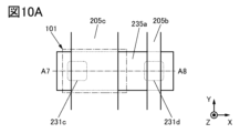
- FIG. 10A is a top view showing a configuration example of a semiconductor device.
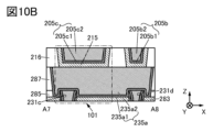
- FIG. 10B is a cross-sectional view showing a configuration example of a semiconductor device.
- FIG. 11 is a cross-sectional view showing a configuration example of a semiconductor device.
- FIG. 12 is a cross-sectional view showing a configuration example of a semiconductor device.
- FIG. 10A is a top view showing a configuration example of a semiconductor device.
- FIG. 10B is a cross-sectional view showing a configuration example of a semiconductor device.
- FIG. 11 is a cross-sectional
- FIG. 13 is a cross-sectional view showing a configuration example of a semiconductor device.
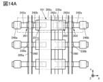
- 14A and 14B are top views showing a configuration example of a semiconductor device.
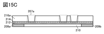
- 15A to 15E are cross-sectional views illustrating an example of a method for manufacturing a semiconductor device.
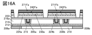
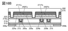
- 16A to 16C are cross-sectional views illustrating an example of a method for manufacturing a semiconductor device.
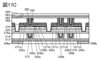
- 17A to 17C are cross-sectional views showing an example of a method for manufacturing a semiconductor device.
- 18A to 18C are cross-sectional views illustrating an example of a method for manufacturing a semiconductor device.
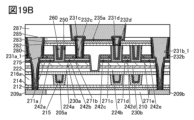
- 19A and 19B are cross-sectional views illustrating an example of a method for manufacturing a semiconductor device.
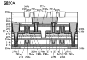
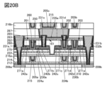
- 20A and 20B are cross-sectional views showing an example of a method for manufacturing a semiconductor device.
- FIG. 21 is a cross-sectional view showing an example of a method for manufacturing a semiconductor device.
- 22A and 22B are diagrams illustrating an example of a storage device.
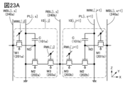
- 23A and 23B are circuit diagrams showing an example of a storage layer.
- FIG. 24 is a timing chart for explaining an example of the operation of a memory cell.
- 25A and 25B are circuit diagrams for explaining an example of the operation of a memory cell.
- 26A and 26B are circuit diagrams for explaining an example of the operation of a memory cell.
- FIG. 27 is a circuit diagram for explaining a configuration example of a semiconductor device.
- 28A and 28B are diagrams showing multi-gate transistors.
- 28C is a circuit diagram showing an example of a memory cell.
- 29A and 29B are diagrams showing an example of a semiconductor device.
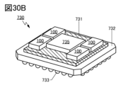
- 30A and 30B are diagrams showing an example of an electronic component.
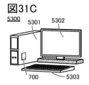
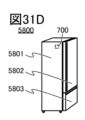
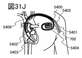
- 31A to 31J are diagrams illustrating an example of an electronic device.
- 32A to 32E are diagrams illustrating an example of an electronic device.
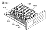
- 33A to 33C are diagrams illustrating an example of an electronic device.
- FIG. 34 is a diagram showing an example of space equipment.
- 35A and 35B are diagrams illustrating an example of medical equipment.
- FIG. 36 is a diagram illustrating the evaluation environment of the X-ray irradiation test.
- FIGS. 37A and 37B are cross-sectional STEM images of the prepared sample.
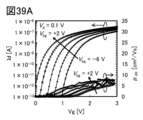
- FIG. 39A is a diagram showing Id-Vg characteristics of a prototype transistor.
- FIG. 39B is a diagram showing the back gate voltage dependence of SS.
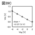
- FIG. 39C is a diagram showing the back gate voltage dependence of Vth.
- FIG. 40A is a diagram showing Id-Vg characteristics of a prototype transistor.
- FIG. 40B is a diagram showing the temperature dependence of SS.
- FIG. 40C is a diagram showing the temperature dependence of Vth.
- FIG. 41A is a diagram showing Id-Vg characteristics of an OS transistor.
- FIG. 41B is a diagram illustrating variations in SS due to X-ray irradiation.
- FIG. 41C is a diagram illustrating changes in ⁇ FE due to X-ray irradiation.
- FIG. 42A is a diagram showing the amount of variation in the threshold voltage of the OS transistor.
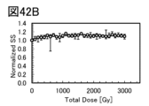
- FIG. 42B is a diagram showing the amount of variation in SS of the OS transistor.
- FIG. 42C is a diagram showing the amount of variation in field effect mobility of the OS transistor.
- 43A and 43B are diagrams showing the amount of variation in the threshold voltage of the OS transistor.
- FIG. 44 is a diagram showing the amount of variation in the threshold voltage of the OS transistor.
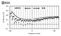
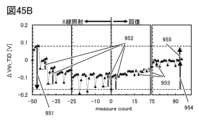
- 45A and 45B are diagrams showing the amount of variation in the threshold voltage of the OS transistor.
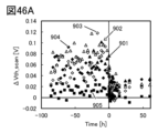
- 46A and 46B are diagrams showing the amount of variation in the threshold voltage of the OS transistor.
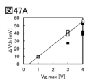
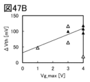
- FIG. 47A to 47D are diagrams showing the gate voltage dependence of TID deterioration components.
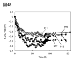
- FIG. 48 is a diagram showing the amount of variation in the threshold voltage of the OS transistor.
- FIG. 49 is a diagram showing the amount of variation in the threshold voltage of the OS transistor.
- FIG. 50 is a diagram showing the amount of variation in the threshold voltage of the OS transistor.
- FIG. 51 is a diagram showing the amount of variation in the threshold voltage of the OS transistor.
- FIG. 52 is a diagram showing the amount of variation in the threshold voltage of the OS transistor.
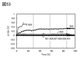
- FIG. 53 is a diagram showing the amount of variation in the threshold voltage of the OS transistor.
- 54A and 54B are diagrams showing the amount of variation in the threshold voltage of the OS transistor.
- 55A and 55B are diagrams showing the gate voltage dependence of the amount of variation in the threshold voltage of an OS transistor.
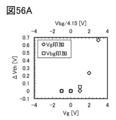
- 56A and 56B are diagrams showing the gate voltage dependence of the amount of variation in the threshold voltage of the OS transistor.
- FIG. 57 is a diagram showing the amount of variation in the threshold voltage of the OS transistor.
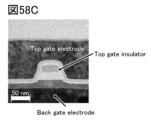
- 58A to 58C are cross-sectional STEM images of an OS transistor.
- 59A and 59B are diagrams showing Id-Vg characteristics of an OS transistor.
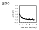
- FIG. 59C is a diagram showing the amount of variation in the threshold voltage of the OS transistor.
- FIG. 60A is a circuit diagram illustrating a memory cell.
- FIG. 60B is a circuit diagram illustrating the readout circuit.
- FIG. 61A is a flowchart showing a TID resistance test method.
- FIG. 61B is a flowchart illustrating the SEU resistance test method.
- FIGS. 62A and 62B are diagrams showing the results of the TID resistance test.
- 63A to 63C are diagrams illustrating error modes occurring in the OS memory.
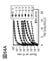
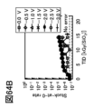
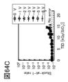
- 64A to 64D are diagrams showing the results of the TID resistance test.
- FIG. 65A is a diagram showing the results of the SEU resistance test.
- FIG. 65B is an error map of SEU in OS memory.
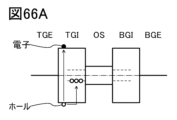
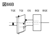
- 66A to 66C are energy band diagrams of OS transistors.
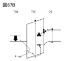
- 67A and 67B are energy band diagrams of OS transistors.
- 68A to 68C are diagrams illustrating error modes occurring in the OS memory.
- ordinal numbers such as “first” and “second” are used for convenience, and do not limit the number of components or the order of the components (for example, the order of steps or the order of lamination). It's not something you do. Further, the ordinal number attached to a constituent element in a certain part of this specification may not match the ordinal number attached to the constituent element in another part of this specification or in the claims.
- film and “layer” can be interchanged depending on the situation or circumstances.
- conductive layer can be changed to the term “conductive film.”
- insulating film can be changed to the term “insulating layer.”
- the term “insulator” can be replaced with an insulating film or an insulating layer.
- the term “conductor” can be replaced with a conductive film or a conductive layer.
- the term “semiconductor” can be translated as a semiconductor film or a semiconductor layer.
- oxynitride refers to a material whose composition contains more oxygen than nitrogen
- nitrided oxide refers to a material whose composition contains more nitrogen than oxygen.
- silicon oxynitride refers to a material whose composition contains more oxygen than nitrogen
- silicon nitride oxide refers to a material whose composition contains more nitrogen than oxygen. shows.
- the heights match refers to a configuration in which the heights from a reference surface (for example, a flat surface such as a substrate surface) are equal in cross-sectional view.
- a reference surface for example, a flat surface such as a substrate surface
- the surface of a single layer or a plurality of layers may be exposed by performing a planarization process (typically a CMP (Chemical Mechanical Polishing) process).
- CMP Chemical Mechanical Polishing
- the surfaces to be subjected to CMP processing have the same height from the reference surface.
- the heights of the plurality of layers may differ depending on the processing apparatus, processing method, or material of the surface to be processed during CMP processing.
- the heights match In this specification, this case is also treated as "the heights match.”
- the height of the top surface of the first layer and the height of the second layer are If the difference from the height of the top surface of the layer is 20 nm or less, it is also said that the heights match.
- the ends coincide means that at least a portion of the outlines of the stacked layers overlap when viewed from above. For example, this includes a case where the upper layer and the lower layer are processed using the same mask pattern or partially the same mask pattern. However, strictly speaking, the contours do not overlap, and the contour of the upper layer may be located inside the contour of the lower layer, or the contour of the upper layer may be located outside the contour of the lower layer. "Concordance”.
- match includes both a complete match and a general match.
- the code when the same code is used for multiple elements, especially when it is necessary to distinguish between them, the code includes an identifying symbol such as "_1", “[n]”, “[m,n]”, etc. In some cases, the symbol may be added to the description. In addition, in the drawings, etc., when a code for identification such as “_1”, “[n]”, “[m,n]”, etc. is added to the code, when there is no need to distinguish it in this specification etc. In some cases, no identification code is written.
- the expression that a layer, wiring, structure, etc. extends in a certain direction means that the layer, wiring, structure, etc. is arranged so as to extend in that direction. Note that when viewed from above, the layer, wiring, structure, etc. only needs to have a shape that extends in the relevant direction; may have portions extending in different directions.
- One embodiment of the present invention relates to a semiconductor device in which a memory layer is provided over a substrate.
- the storage layer includes first to third transistors and a capacitor, and can constitute a memory cell.
- a semiconductor device according to one embodiment of the present invention includes a memory cell and therefore has a function of storing data. Therefore, the semiconductor device of one embodiment of the present invention can be called a memory device.
- the first transistor includes a first metal oxide, first and second conductors on the first metal oxide, and a first conductor between the first conductor and the second conductor. a first insulator on a metal oxide; and a third conductor on the first insulator.
- the second transistor includes a second metal oxide, fourth and fifth conductors on the second metal oxide, and a second conductor between the fourth conductor and the fifth conductor. a second insulator on a metal oxide, and a sixth conductor on the second insulator.
- the third transistor includes a second metal oxide, fifth and seventh conductors on the second metal oxide, and a second conductor between the fifth conductor and the seventh conductor. a third insulator on a metal oxide; and an eighth conductor on the third insulator.
- the second transistor and the third transistor share the second metal oxide and the fifth conductor.
- the first metal oxide and each of the first and second conductors are electrically connected.
- the second metal oxide and each of the fourth and fifth conductors are electrically connected.
- the second metal oxide and each of the fifth and seventh conductors are electrically connected.
- the first metal oxide has a region that functions as a channel formation region of the first transistor.
- the first conductor has a region that functions as one of a source electrode and a drain electrode of the first transistor.
- the second conductor has a region that functions as the other of the source electrode and drain electrode of the first transistor.
- the third conductor has a region that functions as a gate electrode of the first transistor.
- the first insulator has a region that functions as a gate insulator for the first transistor.
- the second metal oxide has a region that functions as a channel formation region of the second transistor and a region that functions as a channel formation region of the third transistor.
- the fourth conductor has a region that functions as one of a source electrode and a drain electrode of the second transistor.
- the fifth conductor has a region that functions as the other of the source electrode and drain electrode of the second transistor and one of the source electrode and drain electrode of the third transistor.
- the sixth conductor has a region that functions as a gate electrode of the second transistor.
- the seventh conductor has a region that functions as the other of the source electrode and drain electrode of the third transistor.
- the eighth conductor has a region that functions as a gate electrode of the third transistor.
- the second insulator has a region that functions as a gate insulator for the second transistor.
- the third insulator has a region that functions as a gate insulator of the third transistor.
- the second transistor and the third transistor are adjacent to each other and share the second metal oxide and the fifth conductor, so that an area smaller than the area of two transistors (for example, 1.5 Two transistors can be formed in a single area (one area).
- transistors can be arranged with high density, and high integration in semiconductor devices can be achieved.
- a semiconductor device of one embodiment of the present invention includes a transistor (OS transistor) that includes a metal oxide in a region where a channel is formed (also referred to as a channel formation region).
- OS transistors have a small off-state current, so when used in a semiconductor device that can be used as a memory device, it is possible to retain memory content for a long period of time. In other words, since no refresh operation is required or the frequency of refresh operations is extremely low, the power consumption of the semiconductor device can be sufficiently reduced. Therefore, a semiconductor device with low power consumption can be provided. Further, since the frequency characteristics of the OS transistor are high, the semiconductor device can read and write data at high speed. Therefore, a semiconductor device with high operating speed can be provided.
- the fourth conductor included in the second transistor is provided extending in the channel width direction (direction perpendicular to the channel length direction) of the second transistor, and is used as a wiring. It has a functional area. With this configuration, there is no need to separately provide an electrode (wiring or plug) connected to one of the source electrode and drain electrode of the second transistor. Note that since the second metal oxide and the fourth conductor of the second transistor are processed using the same mask pattern, the second metal oxide is placed below the fourth conductor. Ru. Therefore, the region of the second metal oxide that overlaps with the fourth conductor is provided to extend in the channel width direction of the second transistor.
- a plurality of memory layers having the above structure are provided in a stacked manner. That is, a plurality of memory layers having the above configuration are provided, for example, in a direction perpendicular to the substrate surface.
- the storage capacity of the semiconductor device can be increased without increasing the area occupied by the memory cells, compared to the case where the storage layer is one layer. Therefore, the area occupied by one bit is reduced, and a small semiconductor device with a large storage capacity can be realized.
- each of the write bit line and the read bit line can be provided, for example, in a direction perpendicular to the substrate surface.
- connection electrodes formed by vertically connecting conductors of the n storage layers are connected in the vertical direction. It can be used as a write bit line and a read bit line extending to the same area.
- a conductor having a region functioning as a write bit line is provided so as to have a region in contact with the top surface and side surfaces of the first conductor.
- a conductor having a region functioning as a read bit line is provided so as to have a region in contact with the top surface and side surfaces of the seventh conductor.
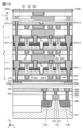
- FIG. 1 is a cross-sectional view illustrating a configuration example of a semiconductor device according to one embodiment of the present invention.
- the semiconductor device shown in FIG. 1 includes an insulator 210 on a substrate (not shown), a conductor 209a and a conductor 209b embedded in the insulator 210, an insulator 212 on the insulator 210, and an insulator 212 on the insulator 210.
- the upper insulator 214 and the n-layer memory layer 11 (memory layer 11_1 to memory layer 11_n) on the insulator 214 are provided extending in the Z direction (also referred to as the vertical direction), and are electrically connected to the conductor 209a.
- connection electrode 240a electrically connected to the conductor 209b
- connection electrode 240b electrically connected to the conductor 209b
- the insulator 181 on the storage layer 11_n the insulator 183 on the insulator 181
- connection electrode 240b electrically connected to the conductor 209b.
- An insulator 185 Note that each of the components included in the semiconductor device of this embodiment may have a single layer structure or a laminated structure.
- a memory cell array having a plurality of memory cells is provided in each of the memory layers 11_1 to 11_n.
- the memory cell includes a transistor 201, a transistor 202, a transistor 203, and a capacitor 101. Furthermore, the connection electrode 240a has a region that functions as a write bit line, and the connection electrode 240b has a region that functions as a read bit line.
- the direction parallel to the channel length direction of the illustrated transistor is defined as the X direction
- the direction parallel to the channel width direction of the illustrated transistor is defined as the Y direction.
- the X direction and the Y direction may be perpendicular to each other.
- a direction perpendicular to both the X direction and the Y direction that is, a direction perpendicular to the XY plane is defined as the Z direction.
- the X direction and the Y direction may be parallel to the substrate surface
- the Z direction may be perpendicular to the substrate surface.
- connection electrode 240a and the connection electrode 240b is formed by connecting conductors of each of the n-layer storage layers 11 in the Z direction.
- the connection electrode 240a is formed by connecting the conductor 231a_1 of the memory layer 11_1, the conductor 231a_2 of the memory layer 11_2, the conductor 231a_3 of the memory layer 11_3, etc. in the Z direction.
- the connection electrode 240b is formed by connecting the conductor 231b_1 of the memory layer 11_1, the conductor 231b_2 of the memory layer 11_2, the conductor 231b_3 of the memory layer 11_3, etc. in the Z direction.
- the conductor 209a and the conductor 209b function as part of a circuit element such as a switch, a transistor, a capacitor, an inductor, a resistance element, and a diode, or as a wiring, an electrode, or a terminal.
- a circuit element such as a switch, a transistor, a capacitor, an inductor, a resistance element, and a diode, or as a wiring, an electrode, or a terminal.
- a storage layer 11_1 which is the lowest layer, a storage layer 11_2 above the storage layer 11_1, and a storage layer 11_n which is the top layer are shown.
- the conductor 209a and the conductor 209b are electrically connected to a drive circuit for driving a memory cell provided in a storage layer of a semiconductor device.
- the drive circuit is provided below the conductor 209a and the conductor 209b.
- the transistors 201 to 203 are provided on an insulator 214. Here, the transistor 202 and the transistor 203 share some layers. A capacitor 101 is provided above the transistors 201 to 203.
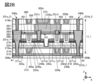
- FIGS. 2A and 2B are a top view and a cross-sectional view, respectively, showing configuration examples of the conductor 209a, the conductor 209b, the insulator 210, the insulator 212, the insulator 214, and the memory layer 11_1.
- FIG. 2B is a cross-sectional view of a portion indicated by a dashed line A1-A2 in FIG. 2A, and is also a cross-sectional view of the transistors 201 to 203 in the channel length direction. Note that in the top view of FIG. 2A, some elements are omitted for clarity.
- an insulator 216a and an insulator 215 are provided over the insulator 214, an insulator 282 is provided over the transistors 201 to 203, an insulator 283 is provided over the insulator 282, and an insulator 283 is provided over the insulator 282.
- a capacitor 101 is provided on the body 283.
- Each of the transistors 201 to 203 includes a conductor 205a on an insulator 214, an insulator 222 on the conductor 205a, an insulator 224 on the insulator 222, and a metal oxide 230 on the insulator 224. It has a pair of conductors 242 on the metal oxide 230, an insulator 250 on the metal oxide 230 between the pair of conductors 242, and a conductor 260 on the insulator 250.
- the transistor 201 includes an insulator 224a as an insulator 224, a metal oxide 230a as a metal oxide 230, and a conductor 242a and a conductor 242b as a pair of conductors 242.
- the transistor 202 includes an insulator 224b as an insulator 224, a metal oxide 230b as a metal oxide 230, and a conductor 242c and a conductor 242d as a pair of conductors 242.
- the transistor 203 includes an insulator 224b as an insulator 224, a metal oxide 230b as a metal oxide 230, and a conductor 242d and a conductor 242e as a pair of conductors 242.
- the transistor 202 and the transistor 203 share an insulator 224b, a metal oxide 230b, and a conductor 242d.
- a plurality of openings reaching the insulator 214 are provided in the insulator 216a. Furthermore, an insulator 215 and a conductor 205a are arranged inside each of the plurality of openings.
- the insulator 215 is provided in contact with the side wall of the opening and the top surface of the insulator 214 .
- the conductor 205a is provided so as to fill the recess formed in the insulator 215.
- the top surface of the conductor 205a matches the height of the top surface of the insulator 215 and the top surface of the insulator 216a, respectively.
- the conductor 205a has a region overlapping with the metal oxide 230a or the metal oxide 230b via the insulator 222 and the insulator 224.
- opening also includes grooves, slits, and the like. Further, a portion in which an opening is formed may be referred to as an opening.
- An insulator 222 is provided on the conductor 205a, the insulator 215, and the insulator 216a. Further, an insulator 275 is provided on the insulator 222 and the conductors 242a to 242e, and an insulator 280 is provided on the insulator 275.
- Each of the transistors 201 to 203 has a pair of insulators 271 between an insulator 275 and a pair of conductors 242.
- the transistor 201 includes an insulator 271a and an insulator 271b as a pair of insulators 271.
- the transistor 202 includes an insulator 271c and an insulator 271d as a pair of insulators 271.
- the transistor 203 includes an insulator 271d and an insulator 271e as a pair of insulators 271.
- the transistor 202 and the transistor 203 share an insulator 271d.
- the insulator 280 and the insulator 275 are provided with an opening that reaches the metal oxide 230a and an opening that reaches the metal oxide 230b. That is, the openings provided in the insulator 280 and the insulator 275 have regions that overlap with the metal oxide 230a or the metal oxide 230b.
- An insulator 250 and a conductor 260 are provided inside the opening. That is, the conductor 260 has a region that overlaps with the metal oxide 230a or the metal oxide 230b with the insulator 250 interposed therebetween.
- the insulator 250 has a region in contact with the sidewall of the opening, and a region in contact with the top surface and side surface of the metal oxide 230a or the metal oxide 230b. Further, the top surface of the conductor 260 matches the height of the top surface of the insulator 250 and the top surface of the insulator 280, respectively.
- An insulator 282 is provided on the insulator 280, the insulator 250, and the conductor 260, an insulator 283 is provided on the insulator 282, and an insulator 285 is provided on the insulator 283.
- the metal oxide 230a has a region that functions as a channel formation region of the transistor 201.
- the metal oxide 230b has a region that functions as a channel formation region of the transistor 202 and a region that functions as a channel formation region of the transistor 203.
- a semiconductor such as single crystal silicon, polycrystalline silicon, or amorphous silicon may be used instead of the metal oxide 230; for example, low temperature polysilicon (LTPS) may be used. Silicon) may also be used.
- the conductor 242a has a region that functions as one of a source electrode and a drain electrode of the transistor 201.
- the conductor 242b has a region that functions as the other of the source electrode and the drain electrode of the transistor 201.
- the conductor 242c has a region that functions as one of a source electrode and a drain electrode of the transistor 202.
- the conductor 242d has a region that functions as the other of the source electrode and the drain electrode of the transistor 202, and a region that functions as one of the source electrode and the drain electrode of the transistor 203.
- the conductor 242e has a region that functions as the other of the source electrode and the drain electrode of the transistor 203.
- the conductor 260 has a region that functions as a first gate electrode of the transistor 201, the transistor 202, or the transistor 203.
- the insulator 250 has a region that functions as a first gate insulator of the transistor 201, the transistor 202, or the transistor 203.
- the conductor 205a has a region that functions as the second gate electrode of the transistor 201, the transistor 202, or the transistor 203.
- the insulator 222 and the insulator 224a have a region that functions as a second gate insulator of the transistor 201.
- the insulator 222 and the insulator 224b have a region that functions as a second gate insulator of the transistor 202 and a region that functions as a second gate insulator of the transistor 203.
- the first gate electrode can be referred to as a top gate electrode or simply a gate electrode
- the second gate electrode can be referred to as a back gate electrode.
- the first gate electrode may be referred to as a back gate electrode
- the second gate electrode may be referred to as a top gate electrode or simply a gate electrode.
- the transistor 202 and the transistor 203 are adjacent to each other and share the metal oxide 230b and the conductor 242d.
- two transistors (the transistor 202 and the transistor 203) can be formed in an area smaller than the area of two transistors (for example, an area of 1.5 transistors). Therefore, the transistors can be arranged at a higher density than when the transistors 202 and 203 do not share the metal oxide 230b and the conductor 242d, and higher integration in the semiconductor device can be achieved.
- a conductor 242d is arranged in a region between the conductor 260 of the transistor 202 and the conductor 260 of the transistor 203. Therefore, an n-type region (low resistance region) can be formed in the region of the metal oxide 230b overlapping with the conductor 242d. Further, a current can also be caused to flow between the transistor 202 and the transistor 203 via the conductor 242d. Therefore, the resistance component between the transistors 202 and 203 can be extremely reduced compared to a configuration in which two transistors using silicon in the semiconductor layer in which a channel is formed (also referred to as Si transistors) are connected in series. .
- the capacitor 101 includes a conductor 235a, an insulator 215 on the conductor 235a, and a conductor 205c on the insulator 215.
- the conductor 235a is provided on the insulator 283 and on the conductor 260 included in the transistor 202. Further, the conductor 235a is electrically connected to the conductor 260.
- An insulator 287 is provided on the insulator 285. Insulator 287 and insulator 285 are provided with openings that reach insulator 283 . Furthermore, a conductor 235a is embedded inside the opening. Here, the top surface of the conductor 235a and the top surface of the insulator 287 match in height.
- An insulator 216b is provided on the conductor 235a and the insulator 287.
- the insulator 216b is provided with a first opening and a plurality of second openings that reach at least one of the insulator 287 and the conductor 235a.
- the first opening has a region overlapping with the conductor 235a, and each of the plurality of second openings has a region overlapping with any one of the transistors 201 to 203.
- An insulator 215 and a conductor 205c are provided inside the first opening, and an insulator 215 and a conductor 205b are provided inside the second opening.
- the insulator 215 is provided in contact with the side and bottom surfaces of each of the first and second openings.
- the conductor 205c is provided so as to fill a recess formed in the insulator 215 provided inside the first opening. At this time, the conductor 205c has a region that overlaps with the conductor 235a with the insulator 215 in between.
- the conductor 205b is provided so as to fill a recess formed in the insulator 215 provided inside the second opening.
- the top surface of the conductor 205c is at the same height as the top surface of the insulator 215, the top surface of the insulator 216b, and the top surface of the conductor 205b.
- the insulator 216b of the memory layer 11_1 is also the insulator 216a of the memory layer 11_2. Therefore, in this specification and the like, the insulator 216b may be replaced with the insulator 216a.
- the conductor 205b of the memory layer 11_1 is also the conductor 205a of the memory layer 11_2. Therefore, the conductor 205b of the memory layer 11_1 has a region that functions as the second gate electrode of the transistor 201, the transistor 202, or the transistor 203 of the memory layer 11_2. Further, the conductor 205b of the memory layer 11_1 has a region overlapping with the metal oxide 230a or the metal oxide 230b of the memory layer 11_2. Note that in this specification and the like, the conductor 205b may be replaced with the conductor 205a.
- conductor 205 when describing matters common to the conductors 205a to 205c, they may be referred to as the conductor 205.
- the conductor 235a has a region that functions as one electrode (also referred to as a lower electrode) of the capacitor 101.
- the insulator 215 has a region that functions as a dielectric of the capacitor 101.
- the conductor 205c has a region that functions as the other electrode (also referred to as an upper electrode) of the capacitor 101.
- the capacitor 101 constitutes an MIM (Metal-Insulator-Metal) capacitor.
- Openings reaching the conductor 242b are provided in the insulators 285, 283, 282, 280, 275, and 271b, and the conductor 231c is embedded inside the openings. Further, the insulator 285, the insulator 283, and the insulator 282 are provided with openings that reach the conductor 260 included in the transistor 202, and the conductor 231d is provided inside the openings.
- the conductor 231c electrically connects the conductor 242b and the conductor 235a. Furthermore, the conductor 231d electrically connects the conductor 260 and the conductor 235a included in the transistor 202.
- the conductor 242b having a region functioning as the other of the source electrode and the drain electrode of the transistor 201 has a region functioning as the gate electrode of the transistor 202 via the conductor 231c, the conductor 235a, and the conductor 231d. It is electrically connected to a conductor 260 that has a conductor 260.
- the conductor 235a has a region in contact with the upper surface of the conductor 231c and a region in contact with the upper surface of the conductor 231d.
- Insulator 285, insulator 283, insulator 282, insulator 280, insulator 275, insulator 222, insulator 216a, insulator 214, and insulator 212 are provided with openings that reach conductor 209a.
- a conductor 231a_1 is embedded inside the opening.
- the insulator 285, insulator 283, insulator 282, insulator 280, insulator 275, and insulator 222 of the memory layer 11_2 (not shown), as well as the insulator 216b and the insulator 287, include the conductor 231a_1.
- An opening is provided, and a conductor 231a_2 is embedded inside the opening.
- connection electrode 240a includes a conductor 231a_1 and a conductor 231a_2.
- the insulators 285, 283, 282, 280, 275, 222, 216a, 214, and 212 are provided with openings that reach the conductor 209b.
- a conductor 231b_1 is embedded inside the opening.
- the insulator 285, insulator 283, insulator 282, insulator 280, insulator 275, and insulator 222 of the memory layer 11_2 (not shown), as well as the insulator 216b and the insulator 287, include the conductor 231b_1.
- An opening is provided to reach the conductor 231b_2, and a conductor 231b_2 is embedded inside the opening.
- connection electrode 240b includes a conductor 231b_1 and a conductor 231b_2.
- the top surface of the conductor 231c, the top surface of the conductor 231d, the top surface of the conductor 231a_1, and the top surface of the conductor 231b_1 have the same height. Further, the conductor 231c, the conductor 231d, the conductor 231a_1, and the conductor 231b_1 can be formed using the same material and in the same process. Therefore, it is preferable that the conductor 231c, the conductor 231d, the conductor 231a_1, and the conductor 231b_1 have the same conductive material.
- the conductor 231a when describing matters common to the conductor 231a_1 and the conductor 231a_2, they may be referred to as the conductor 231a.
- the conductor 231b When describing matters common to the conductor 231b_1 and the conductor 231b_2, the conductor 231b may be referred to as the conductor 231b.
- FIG. 2B shows a configuration in which the insulator 216a is not provided with a conductor corresponding to the conductor 205c provided in the insulator 216b.
- the present invention is not limited to this.
- an insulator 215 and a conductor corresponding to the conductor 205c provided in the insulator 216b may be provided on the insulator 216a.
- the mask used when forming the opening in the insulator 216a and the mask used when forming the opening in the insulator 216b can be shared, so that manufacturing costs can be reduced.
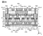
- FIG. 2B shows a configuration in which an insulator 215 is provided between the insulator 216a and the conductor 205a. Note that the present invention is not limited to this. For example, as shown in FIG. 3B, a configuration may be adopted in which the insulator 215 is not provided. By not providing the insulator 215, manufacturing costs can be reduced.
- FIG. 2B shows a configuration in which the upper surface of the conductor 231a_1 is in contact with the lower surface of the conductor 231a_2 and the upper surface of the conductor 231b_1 is in contact with the lower surface of the conductor 231b_2, the present invention is not limited to this.
- a conductor 231a_1 and a conductor 231a_2 may be connected via a conductor 235b
- a conductor 231b_1 and a conductor 231b_2 may be connected via a conductor 235c.
- a conductor 235a, a conductor 235b, and a conductor 235c are provided inside an opening formed in an insulator 287.
- the conductor 235b has a region in contact with the upper surface of the conductor 231a_1 and a region in contact with the lower surface of the conductor 231a_2.
- the conductor 235c has a region in contact with the upper surface of the conductor 231b_1 and a region in contact with the lower surface of the conductor 231b_2.
- FIG. 2B shows a configuration in which the components of the semiconductor device have a single layer structure
- the present invention is not limited to this. Some of the components included in the semiconductor device may have a stacked structure.
- FIG. 3B shows a configuration in which conductors 205b are provided in the insulators 216b in regions overlapping with the transistors 201 to 203, the present invention is not limited to this.
- a structure may be adopted in which the conductor 205b is not provided in the insulator 216b in a region overlapping with the transistor 202.
- the conductor 205c has a region that overlaps with the transistor 202.
- the conductor 205c is shared by the capacitor 101 and the transistor 202.
- the conductor 205c has a region that functions as the other electrode of the capacitor 101 and a region that functions as the second gate electrode of the transistor 202.
- an electric field generated outside the transistor 202 such as static electricity, can be prevented from acting on the metal oxide 230b. Therefore, it is possible to suppress variations in the electrical characteristics of the transistor due to the influence of an external electric field. Therefore, reliability of the semiconductor device can be improved.
- a configuration may be adopted in which the conductor 205b is not provided on the insulator 216b.
- the conductor 205c has a region overlapping with the transistors 201 to 203.
- the conductor 205c is shared by the capacitor 101 and the transistors 201 to 203.
- the conductor 205c has a region that functions as the other electrode of the capacitor 101 and a region that functions as the second gate electrode of each of the transistors 201 to 203.
- the area of the region where the conductor 205c and the conductor 235a overlap, the area of the region where the conductor 205c and the metal oxide 230a overlap, and the area of the region where the conductor 205c and the metal oxide 230b overlap are increased.
- the entire metal oxide can be overlapped with the conductor 205 in plan view.
- the capacitance of the capacitor 101 can be increased, and fluctuations in electrical characteristics due to the influence of an electric field generated outside the transistors 201 to 203 can be suitably suppressed.
- the semiconductor device shown in FIG. 2B can change the potentials of the second gate electrodes of the transistors 201 to 203 independently without interlocking with the potential of the other electrode of the capacitor 101. Therefore, the threshold voltages (Vth) of the transistors 201 to 203 can be controlled.
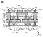
- each of a conductor 205, a metal oxide 230, a conductor 242, an insulator 271, an insulator 250, a conductor 260, conductors 231a to 231d, and a conductor 235a has a laminated structure. It becomes. Note that a preferable laminated structure of the constituent elements will be described later.
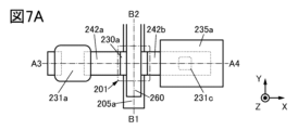
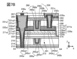
- FIG. 7B is a cross-sectional view showing a configuration example of a semiconductor device.
- a top view corresponding to the cross-sectional view of FIG. 7B is shown in FIG. 7A.
- FIG. 7B is a cross-sectional view of a portion indicated by a dashed line A3-A4 in FIG. 7A, and is also a cross-sectional view of the transistor 201 in the channel length direction.
- FIG. 7C is a cross-sectional view of the portion indicated by the dashed line B1-B2 in FIG. 7A, and is also a cross-sectional view of the transistor 201 in the channel width direction. Note that in the top view of FIG. 7A, some elements are omitted for clarity.
- the top and side surfaces of the metal oxide 230a and the side surfaces of the insulator 224a are covered with an insulator 250 and a conductor 260.
- the insulator 250 and the conductor 260 are provided inside the opening 258a that the insulator 280 and the insulator 275 have.
- a curved surface may be provided between the side surface of the metal oxide 230a and the top surface of the metal oxide 230a. That is, the end of the side surface and the end of the top surface may be curved (hereinafter also referred to as round shape).
- a conductor 260 having a region functioning as a first gate electrode.
- the conductor 205a is preferably provided larger than the area of the metal oxide 230a that does not overlap with the conductors 242a and 242b.
- the conductor 205a preferably extends also in a region outside the end of the metal oxide 230a in the channel width direction. That is, on the outside of the side surface of the metal oxide 230a in the channel width direction, the conductor 205a and the conductor 260 preferably overlap with each other with an insulator in between.
- the channel formation region of the metal oxide 230a is electrically surrounded by the electric field of the conductor 260 functioning as the first gate electrode and the electric field of the conductor 205a functioning as the second gate electrode. be able to.
- a structure of a transistor in which a channel formation region is electrically surrounded by at least the electric field of the first gate electrode is referred to as a surrounded channel (S-channel) structure.
- the S-channel structure disclosed in this specification and the like has a structure different from the Fin type structure and the planar type structure.
- the S-channel structure disclosed in this specification and the like can also be regarded as a type of Fin type structure.
- a Fin type structure refers to a structure in which a gate electrode is arranged so as to surround at least two or more surfaces (specifically, two, three, or four sides) of a channel.
- the channel formation region can be electrically surrounded.
- the S-channel structure is a structure that electrically surrounds the channel formation region, it is substantially equivalent to a GAA (Gate All Around) structure or an LGAA (Lateral Gate All Around) structure. You can say that.
- the transistor has an S-channel structure, a GAA structure, or an LGAA structure, the channel formation region formed at or near the interface between the oxide and the gate insulator can be formed in the entire bulk of the oxide. Therefore, it is possible to improve the current density flowing through the transistor, and thus it is expected that the on-state current of the transistor will be improved or the field effect mobility of the transistor will be increased.
- the transistor illustrated in FIG. 7B has an S-channel structure
- the semiconductor device of one embodiment of the present invention is not limited thereto.
- the transistor structure that can be used in one embodiment of the present invention may be one or more selected from a planar structure, a fin structure, and a GAA structure.
- connection electrode 240a has a region in contact with a part of the upper surface of the conductor 242a and a region in contact with a part of the side surface of the conductor 242a.
- connection electrode 240b has a region in contact with a part of the upper surface of the conductor 242e and a region in contact with a part of the side surface of the conductor 242e.
- the conductor 231a has a region in contact with a part of the upper surface of the conductor 242a and a region in contact with a part of the side surface of the conductor 242a.
- the conductor 231b has a region in contact with a part of the upper surface of the conductor 242e and a region in contact with a part of the side surface of the conductor 242e.
- connection resistance between the connection electrode 240b and the conductor 242e can be reduced by the connection electrode 240b being in contact with multiple surfaces of the conductor 242e. Furthermore, there is no need to provide connection electrodes, and the number of steps in the manufacturing process of the semiconductor device can be reduced.
- FIG. 7A shows a configuration in which the top surface shape of the conductor 231a is a quadrilateral with rounded corners
- the present invention is not limited to this.
- the top surface shape of the conductor 231a may be circular, elliptical, polygonal, or polygonal with rounded corners.
- the polygonal shape refers to a triangle, a quadrilateral, a pentagon, a hexagon, and the like.
- top shape of a certain component refers to the outline shape of the component in plan view.
- planar view refers to viewing from the normal direction of the surface on which the component is formed or the surface of the support (for example, a substrate) on which the component is formed.
- an insulator 232a is provided in contact with the side surface of the conductor 231a.
- a conductor 232a is provided, and a conductor 231a is provided in contact with a portion of the upper surface and a portion of the side surface of the conductor 242a, and a side surface of the insulator 232a.
- the conductor 231a is provided so as to fill the inside of the opening with the insulator 232a interposed therebetween.
- the insulator 232a includes an insulator 285, an insulator 283, an insulator 282, an insulator 280, an insulator 275, an insulator 271a, a metal oxide 230a, an insulator 224a, an insulator 222, and an insulator inside the opening. 216 , the insulator 214 , and the insulator 212 .
- FIG. 8B is a cross-sectional view showing a configuration example of a semiconductor device.
- a top view corresponding to the cross-sectional view of FIG. 8B is shown in FIG. 8A.
- FIG. 8B is a cross-sectional view of a portion indicated by a dashed line A5-A6 in FIG. 8A, and is also a cross-sectional view of the transistor 202 and the transistor 203 in the channel length direction. Note that in the top view of FIG. 8A, some elements are omitted for clarity.
- the cross-sectional view of FIG. 7C can be referred to.
- the cross-sectional view of the transistor 202 in the channel width direction can be referred to, except that the conductor 260 does not extend in the channel width direction.
- an insulator 232b is provided in contact with the side surface of the conductor 231b.
- a conductor 232b is provided, and a conductor 231b is provided in contact with a portion of the upper surface and a portion of the side surface of the conductor 242e, and a side surface of the insulator 232b.
- Insulator 232b includes insulator 285, insulator 283, insulator 282, insulator 280, insulator 275, insulator 271e, metal oxide 230b, insulator 224b, insulator 222, insulator 216 , the insulator 214 , and the insulator 212 .
- FIG. 8C shows a top view including the conductor 242c, the conductor 242d, the conductor 242e, and the metal oxide 230b. Note that in FIG. 8C, the respective outlines of the conductor 260 and the connection electrode 240b are indicated by dotted lines.
- the metal oxide 230b has a first region that overlaps with the conductor 242c and extends in the first direction, a second region that overlaps with the conductor 260 of the transistor 202, and a conductive region. It has a third region that overlaps with the body 242d and a fourth region that overlaps with the conductor 242e.
- the conductor 242c has a region overlapping with the metal oxide 230b
- the conductor 242d has a region overlapping with the metal oxide 230b
- the conductor 242e has a region overlapping with the metal oxide 230b.
- the end of the metal oxide 230b coincides with the end of the conductor 242c.
- the first region has a region extending in the channel width direction (Y direction) of the transistor 202. That is, the first direction is the Y direction.
- the conductor 242c has a region extending in the Y direction. Therefore, the conductor 242c can also function as a wiring.
- a metal oxide 230b is provided below a region of the conductor 242c that functions as a wiring.
- the end of the metal oxide 230b coincides with the end of the conductor 242d. Furthermore, in the fourth region, the end of the metal oxide 230b coincides with the end of the conductor 242e.
- FIGS. 9A and 9B an enlarged view of a part of the connection electrode 240a and its vicinity is shown in FIGS. 9A and 9B.
- FIG. 9A is an enlarged view of a part of the connection electrode 240a and its vicinity in the channel width direction.
- FIG. 9B is an enlarged view of a part of the connection electrode 240a and its vicinity in the channel length direction, and is also an enlarged view of a part of the connection electrode 240a and its vicinity in FIG. 7B.
- the insulator 232a has a region 237a, a region 238a, and a region 239a.
- the region 237a is a region in contact with one or more of the insulators 285, 283, 282, 280, 275, and 271a.
- the region 238a is a region in contact with one or more side surfaces of the metal oxide 230a, the insulator 224a, the insulator 222, the insulator 216, the insulator 214, and the insulator 212.
- Region 239a is a region between region 237a and region 238a.
- insulator 232a contacts the respective side surfaces of insulator 280 and insulator 275 inside the opening in which conductor 231a is provided.
- the width of the region of the conductor 231a included in the connection electrode 240a that is in contact with the side surface of the conductor 242a is defined as width W1.
- the width W1 is the distance between the conductors 242a.
- the width of the region of the conductor 231a of the connection electrode 240a that is in contact with the side surface of the insulator 232a in the region 237a is defined as width W2.
- the width W2 is the distance between the side surfaces of the insulator 232a in the region 237a.
- the width W2 is preferably larger than the width W1.
- the connection electrode 240a is in contact with at least a portion of the upper surface of the conductor 242a. Therefore, the area of the region where the connection electrode 240a and the conductor 242a are in contact can be increased.
- the connection electrode 240b may also have a similar configuration. Note that in this specification and the like, the contact between the connection electrode 240 and the conductor 242 is sometimes referred to as a top side contact.
- the opening in which the connection electrode 240a is provided preferably has a region that overlaps with the conductor 242a. With this configuration, the connection electrode 240a is in contact with at least a portion of the upper surface of the conductor 242a.
- the opening in which the connection electrode 240b is provided preferably has a region that overlaps with the conductor 242e. With this configuration, the connection electrode 240b is in contact with at least a portion of the upper surface of the conductor 242e.
- the top of the insulator 232a in the region 238a is preferably located below the upper surface of the conductor 242a.
- the conductor 231a can come into contact with at least a part of the side surface of the conductor 242a.
- the insulator 232a in the region 238a preferably has a region in contact with the side surface of the metal oxide 230a. With this configuration, it is possible to suppress impurities such as water and hydrogen contained in the insulator 280 and the like from entering the metal oxide 230a through the conductor 231a.
- the above-described positional relationship between the conductor 231a, the conductor 242a, and the insulator 232a is also applied to the conductor 231b, the conductor 242e, and the insulator 232b. Therefore, the above-mentioned conductor 231a, conductor 242a, and insulator 232a can be read as conductor 231b, conductor 242e, and insulator 232b, respectively.
- the insulator 232b has a region corresponding to the region 237a, a region corresponding to the region 238a, and a region corresponding to the region 239a.
- the insulator 232b contacts the respective side surfaces of the insulator 280 and the insulator 275 inside the opening where the conductor 231b is provided.
- FIG. 10B is a cross-sectional view showing a configuration example of a semiconductor device.
- a top view corresponding to the cross-sectional view of FIG. 10B is shown in FIG. 10A.
- FIG. 10B is a cross-sectional view of the portion indicated by the dashed line A7-A8 in FIG. 10A, and is also a cross-sectional view of the transistor 201 in the channel length direction. Note that in the top view of FIG. 10A, some elements are omitted for clarity.
- the conductor 205c has a region that overlaps with the conductor 235a. Further, the conductor 205c is provided extending in the Y direction. That is, the first direction in which the first region of metal oxide 230b extends is parallel to the direction in which conductor 205c extends. Further, as shown in FIG. 10B, the conductor 205c may have a two-layer stacked structure of a conductor 205c1 and a conductor 205c2 on the conductor 205c1. Note that the conductor 205c can be formed using the same material and in the same process as the conductor 205b. Therefore, it is preferable that the conductor 205c1 has the same conductive material as the conductor 205b1. It is preferable that the conductor 205c2 has the same conductive material as the conductor 205b2.
- the metal oxide that functions as a semiconductor is preferably 2.0 eV or more, more preferably 2.5 eV or more.
- metal oxide 230 it is preferable to use metal oxides such as indium oxide, gallium oxide, and zinc oxide. Further, as the metal oxide 230, it is preferable to use a metal oxide having two or three selected from among indium, element M, and zinc, for example.
- Element M is gallium, aluminum, silicon, boron, yttrium, tin, copper, vanadium, beryllium, titanium, iron, nickel, germanium, zirconium, molybdenum, lanthanum, cerium, neodymium, hafnium, tantalum, tungsten, and magnesium.
- the element M is preferably one or more selected from aluminum, gallium, yttrium, and tin.
- a metal oxide containing indium, element M, and zinc may be referred to as an In-M-Zn oxide.
- FIG. 2B shows a configuration in which the metal oxide 230 is a single layer
- the metal oxide 230 may have a laminated structure of two or more layers.
- the metal oxide 230 may have a two-layer stacked structure of a first metal oxide and a second metal oxide on the first metal oxide.
- the metal oxide 230a includes a metal oxide 230a1 as a first metal oxide and a metal oxide 230a2 as a second metal oxide.
- the metal oxide 230b includes a metal oxide 230b1 as a first metal oxide and a metal oxide 230b2 as a second metal oxide.
- the metal oxide 230 has a laminated structure of two or more layers, it is preferable that the metal oxide 230 has a laminated structure of a plurality of oxide layers having different chemical compositions.
- the metal oxide 230 has a two-layer stacked structure, atoms of element M with respect to the metal element that is the main component in the metal oxide used for the first metal oxide.
- the numerical ratio is larger than the atomic ratio of the element M to the metal element that is the main component in the metal oxide used for the second metal oxide.
- the atomic ratio of element M to In may be larger than the atomic ratio of element M to In in the metal oxide used for the second metal oxide. preferable. With this configuration, diffusion of at least one of impurities and oxygen from a structure formed below the first metal oxide to the second metal oxide can be suppressed.
- the atomic ratio of In to the element M may be larger than the atomic ratio of In to the element M in the metal oxide used for the first metal oxide. preferable. With this configuration, the transistor can obtain a large on-current and high frequency characteristics.
- the defect level at the interface between the first metal oxide and the second metal oxide can be reduced. Density can be reduced. Therefore, the influence of interface scattering on carrier conduction is reduced, and the transistor can obtain a large on-current and high frequency characteristics.
- the nearby composition includes a range of ⁇ 30% of the desired atomic ratio.
- the element M it is preferable to use gallium.
- the compositions of the metal oxides that can be used for the first metal oxide and the second metal oxide are not limited to the above.
- a metal oxide composition that can be used for the first metal oxide may be applied to the second metal oxide.
- the metal oxide compositions that can be used for the second metal oxide may be applied to the first metal oxide.
- the metal oxide 230 is a single layer, a metal oxide that can be used as the first metal oxide or the second metal oxide may be used as the metal oxide 230.
- the above atomic ratio is not limited to the atomic ratio of the formed metal oxide, but also the atomic ratio of the sputtering target used for forming the metal oxide film. It may be.
- the second metal oxide of the metal oxide 230 has a channel formation region and a source region and a drain region provided to sandwich the channel formation region in the transistor. At least a portion of the channel forming region overlaps with the conductor 260.
- the source region overlaps with one of the pair of conductors 242, and the drain region overlaps with the other of the pair of conductors 242. Note that the channel formation region, the source region, and the drain region may be formed not only in the second metal oxide of the metal oxide 230 but also in the first metal oxide of the metal oxide 230, respectively.
- a transistor using an oxide semiconductor when impurities and oxygen vacancies are present in a channel formation region in the oxide semiconductor, electrical characteristics tend to fluctuate, and reliability may deteriorate in some cases. Furthermore, hydrogen near the oxygen vacancy may form a defect in which hydrogen is present in the oxygen vacancy (hereinafter sometimes referred to as V OH ), and generate electrons that serve as carriers. Therefore, if the channel formation region in the oxide semiconductor contains oxygen vacancies, the transistor exhibits normally-on characteristics (a channel exists even when no voltage is applied to the gate electrode, and current flows through the transistor). It's easy to become. Therefore, in the channel formation region in the oxide semiconductor, impurities, oxygen vacancies, and V OH are preferably reduced as much as possible.
- the insulator can be converted to an oxide semiconductor. It can supply oxygen and reduce oxygen vacancies and V OH .
- excess oxygen oxygen that is desorbed by heating
- the insulator can be converted to an oxide semiconductor. It can supply oxygen and reduce oxygen vacancies and V OH .
- excess oxygen oxygen that is supplied to the source region or the drain region.
- the on-state current or field effect mobility of the transistor will be reduced.
- the amount of oxygen supplied to the source region or the drain region varies within the substrate plane, resulting in variations in the characteristics of a semiconductor device including a transistor.
- the channel formation region has a reduced carrier concentration and is preferably i-type or substantially i-type, whereas the source and drain regions have a high carrier concentration and are n-type. It is preferable. In other words, it is preferable to reduce oxygen vacancies and V OH in the channel formation region of the oxide semiconductor. Further, it is preferable that an excessive amount of oxygen is not supplied to the source region and the drain region, and that the amount of V OH in the source region and the drain region is not excessively reduced. Further, it is preferable to adopt a structure that suppresses a decrease in the conductivity of the conductor 260, the conductor 242, and the like.
- the channel forming region has fewer oxygen vacancies or has a lower impurity concentration than the source and drain regions, so it is a high resistance region with a lower carrier concentration. Therefore, the channel forming region can be said to be i-type (intrinsic) or substantially i-type.
- the carrier concentration of the channel forming region is 1 ⁇ 10 18 cm ⁇ 3 or less, less than 1 ⁇ 10 17 cm ⁇ 3 , less than 1 ⁇ 10 16 cm ⁇ 3 , less than 1 ⁇ 10 15 cm ⁇ 3 , or 1 ⁇ 10 14 It is preferably less than cm ⁇ 3 , less than 1 ⁇ 10 13 cm ⁇ 3 , less than 1 ⁇ 10 12 cm ⁇ 3 , less than 1 ⁇ 10 11 cm ⁇ 3 , or less than 1 ⁇ 10 10 cm ⁇ 3 . Further, the lower limit of the carrier concentration in the channel forming region is not particularly limited, but can be set to, for example, 1 ⁇ 10 ⁇ 9 cm ⁇ 3 .
- the impurity concentration in the metal oxide 230 is lowered to lower the defect level density.
- the term “high purity intrinsic” or “substantially high purity intrinsic” means that the impurity concentration is low and the defect level density is low.
- an oxide semiconductor (or metal oxide) with a low carrier concentration may be referred to as a high-purity intrinsic or substantially high-purity intrinsic oxide semiconductor (or metal oxide).
- the impurities in the metal oxide 230 refer to, for example, substances other than the main components that constitute the metal oxide.
- an element having a concentration of less than 0.1 atomic % can be considered an impurity.
- examples of impurities in the metal oxide 230 include hydrogen, nitrogen, alkali metals, alkaline earth metals, iron, nickel, and silicon.
- the source region and the drain region are low resistance regions with a high carrier concentration because they have many oxygen vacancies or have a high impurity concentration. That is, the source region and the drain region are n-type regions (low resistance regions) that have a higher carrier concentration than the channel forming region.
- the concentrations of metal elements and impurity elements detected within each region are not limited to a stepwise change from region to region, and may also vary continuously within each region. In other words, the concentration of the impurity element may decrease as the region is closer to the channel formation region.
- the impurity concentration in the metal oxide 230 In order to stabilize the electrical characteristics of the transistor, it is effective to reduce the impurity concentration in the metal oxide 230. Furthermore, in order to reduce the impurity concentration of the metal oxide 230, it is preferable to also reduce the impurity concentration in the adjacent film.
- the second metal oxide of the metal oxide 230 is preferably an oxide semiconductor having crystallinity.
- oxide semiconductors with crystallinity include CAAC-OS (c-axis aligned crystalline oxide semiconductor), nc-OS (nanocrystalline oxide semiconductor), and many others. Examples include crystalline oxide semiconductors, single crystal oxide semiconductors, and the like.
- CAAC-OS c-axis aligned crystalline oxide semiconductor
- nc-OS nanocrystalline oxide semiconductor
- Examples include crystalline oxide semiconductors, single crystal oxide semiconductors, and the like.
- it is preferable to use CAAC-OS or nc-OS it is particularly preferable to use CAAC-OS.
- CAAC-OS is a metal oxide that has a highly crystalline and dense structure and has few impurities and defects (for example, oxygen vacancies).
- heat treatment at a temperature that does not polycrystallize the metal oxide (e.g., 400°C or higher and 600°C or lower) allows CAAC-OS to have a more highly crystalline and dense structure. It can be done. In this way, by further increasing the density of the CAAC-OS, it is possible to further reduce the diffusion of impurities or oxygen in the CAAC-OS.
- CAAC-OS it is difficult to confirm clear grain boundaries, so it can be said that reduction in electron mobility due to grain boundaries is less likely to occur. Therefore, the metal oxide with CAAC-OS has stable physical properties. Therefore, metal oxides with CAAC-OS are resistant to heat and have high reliability.
- the extraction of oxygen from the second metal oxide by the source electrode or drain electrode is suppressed. can.
- oxygen can be suppressed from being extracted from the second metal oxide, so that the transistor is stable against high temperatures (so-called thermal budget) during the manufacturing process. Further, it is possible to suppress the conductivity of the conductor 242 from decreasing.
- the nc-OS has periodicity in the atomic arrangement in a minute region (for example, a region of 1 nm or more and 10 nm or less, particularly a region of 1 nm or more and 3 nm or less).
- the nc-OS has minute crystals (also referred to as nanocrystals).
- no regularity is observed in the crystal orientation between different nanocrystals, so no orientation is observed in the entire film. That is, when an nc-OS is used as the metal oxide 230, the film characteristics of the metal oxide 230 are constant regardless of the direction of carriers flowing in the metal oxide 230, so the electrical characteristics of the transistor are stable.
- the metal oxide 230 includes CAAC-OS, nc-OS, pseudo-amorphous oxide semiconductor (a-like OS), amorphous oxide semiconductor, polycrystalline oxide semiconductor, CAC-OS (cloud-aligned composite oxide semiconductor), two or more types may be included.
- the position of the peak (2 ⁇ value) indicating c-axis orientation may vary depending on the type, composition, etc. of the metal element constituting the CAAC-OS.
- a plurality of bright points (spots) are observed in the electron diffraction pattern of the CAAC-OS film. Note that a certain spot and another spot are observed at positions that are symmetrical with respect to the spot of the incident electron beam that has passed through the sample (also referred to as a direct spot) as the center of symmetry.
- electron beam diffraction also called nanobeam electron diffraction
- an electron beam with a probe diameter equal to or smaller than the nanocrystal for example, from 1 nm to 30 nm
- An electron diffraction pattern in which a plurality of spots are observed within a ring-shaped region centered on the spot may be obtained.
- the metal oxide 230 can be rephrased as a semiconductor layer including the channel formation region of the transistor 201.
- the material applicable to the semiconductor layer is not limited to a metal oxide that functions as a semiconductor (oxide semiconductor).
- a semiconductor such as single crystal silicon, polycrystalline silicon, or amorphous silicon may be used, and for example, LTPS may be used.
- the semiconductor layer may be a transition metal chalcogenide that functions as a semiconductor, such as molybdenum sulfide (typically MoS 2 ), molybdenum selenide (typically MoSe 2 ), molybdenum tellurium (typically MoTe 2 ), tungsten sulfide (typically WS 2 ), tungsten selenide (typically WSe 2 ), tungsten tellurium (typically WTe 2 ), hafnium sulfide (typically HfS 2 ). , hafnium selenide (typically HfSe 2 ), zirconium sulfide (typically ZrS 2 ), zirconium selenide (typically ZrSe 2 ), and the like may be used.
- molybdenum sulfide typically MoS 2
- molybdenum selenide typically MoSe 2
- molybdenum tellurium typically MoTe 2
- insulator 280 In order to supply oxygen to the channel formation region, it is preferable to use an insulator containing excess oxygen as the insulator 280. With this configuration, oxygen contained in the insulator 280 can be supplied to the channel formation region of the metal oxide 230.
- an oxide containing silicon such as silicon oxide, silicon oxynitride, silicon oxide added with fluorine, silicon oxide added with carbon, silicon oxide added with carbon and nitrogen, silicon oxide with holes, etc. It is preferable to use In particular, silicon oxide and silicon oxynitride are preferable because they are thermally stable. Further, materials such as silicon oxide, silicon oxynitride, and silicon oxide having vacancies are preferable because they can easily form a region containing oxygen that is released by heating.
- the insulator 280 functions as an interlayer film, it preferably has a low dielectric constant.
- a material with a low dielectric constant as an interlayer film, parasitic capacitance generated between wirings can be reduced.
- the above-mentioned oxide containing silicon is a material with a low dielectric constant, and is therefore preferable.
- the concentration of impurities such as water and hydrogen in the insulator 280 is reduced.
- the insulator 280 preferably includes silicon oxide or an oxide containing silicon such as silicon oxynitride.
- the side wall of the insulator 280 may be approximately perpendicular to the upper surface of the insulator 222, or may have a tapered shape.
- the side wall for example, the coverage of the insulator 250 provided in the opening of the insulator 280 is improved, and defects such as holes can be reduced.
- the sidewall approximately perpendicular to the upper surface of the insulator 222, it is possible to miniaturize or highly integrate the semiconductor device.
- a tapered shape refers to a shape in which at least a part of the side surface of the structure is inclined with respect to the substrate surface or the surface to be formed. For example, there is a region where the angle between the inclined side surface and the substrate surface or the surface to be formed (hereinafter sometimes referred to as a taper angle) is less than 90°.
- the side surfaces of the structure and the substrate surface do not necessarily have to be completely flat, and may be substantially planar with minute curvatures or substantially planar with minute irregularities.
- the insulator 250 has a region that functions as a first gate insulator.
- FIG. 2B shows a structure in which the insulator 250 is a single layer, the present invention is not limited to this, and may have a laminated structure of two or more layers.
- the insulator 250 may have a three-layer stacked structure of an insulator 250a, an insulator 250b over the insulator 250a, and an insulator 250c over the insulator 250b.
- insulator 250b In order to supply oxygen to the channel formation region, it is preferable to use an insulator that easily transmits oxygen as the insulator 250b. With this configuration, oxygen contained in the insulator 280 can be supplied to the channel formation region of the metal oxide 230 via the insulator 250b.
- the insulator 250b for example, silicon oxide, silicon oxynitride, silicon oxide added with fluorine, silicon oxide added with carbon, silicon oxide added with carbon and nitrogen, silicon oxide with holes, etc. can be used.
- silicon oxide and silicon oxynitride are preferable because they are stable against heat.
- the insulator 250b includes at least oxygen and silicon.
- the concentration of impurities such as water and hydrogen in the insulator 250b is reduced.
- the film thickness of the insulator 250b is preferably 0.5 nm or more and 20 nm or less, more preferably 1 nm or more and 15 nm or less.
- the film thickness of the insulator 250b is preferably 0.5 nm or more and 10 nm or less, and preferably 0.5 nm or more and 5 nm or less. is more preferable.
- the insulator 250b only needs to have a region with the above-mentioned film thickness at least in part.
- the insulator 250a is provided in contact with the lower surface of the insulator 250b, the upper surface of the metal oxide 230, and the side surface of the metal oxide 230.
- the insulator 250a preferably has barrier properties against oxygen. Since the insulator 250a has barrier properties against oxygen, oxygen contained in the insulator 250b can be supplied to the channel formation region, and oxygen contained in the insulator 250b can be prevented from being excessively supplied to the channel formation region. Therefore, it is possible to suppress excessive supply of oxygen to the source region and the drain region through the channel formation region, which would cause a decrease in the on-state current or a decrease in field effect mobility of the transistor.
- the insulator 250a is provided between the insulator 280 and the insulator 250b, and has a region in contact with the side wall of the opening that the insulator 280 has. With this configuration, oxygen contained in the insulator 280 can be supplied to the insulator 250b, and oxygen contained in the insulator 280 can be prevented from being excessively supplied to the insulator 250b.
- an insulator containing oxides of one or both of aluminum and hafnium is preferable to use as the insulator 250a.
- the insulator aluminum oxide, hafnium oxide, an oxide containing aluminum and hafnium (hafnium aluminate), an oxide containing hafnium and silicon (hafnium silicate), or the like can be used.
- the insulator 250a for example, magnesium oxide, gallium oxide, gallium zinc oxide, indium gallium zinc oxide, or the like may be used.
- the insulator 250a may be made of any material that is less permeable to oxygen than the insulator 250b, for example.
- the insulator 250a contains at least oxygen and aluminum.
- Aluminum oxide which can be suitably used as the insulator 250a, has a function of suppressing the diffusion of hydrogen (for example, at least one of hydrogen atoms and hydrogen molecules). Therefore, impurities such as hydrogen contained in the insulator 250b can be suppressed from diffusing into the metal oxide 230.
- the insulator 250a may be made of any material that is less permeable to hydrogen than, for example, the insulator 250b.
- the film thickness of the insulator 250a is preferably thin. By reducing the thickness of the insulator 250a, a fine transistor can be manufactured, and a semiconductor device that can be miniaturized or highly integrated can be provided. Further, by reducing the thickness of the insulator 250a, it is possible to suppress a decrease in the amount of oxygen supplied to the metal oxide 230 via the insulator 250b.
- the film thickness of the insulator 250a is 0.1 nm or more and 5.0 nm or less, preferably 0.5 nm or more and 3.0 nm or less, and more preferably 1.0 nm or more and less than 3.0 nm.
- the insulator 250a only needs to have a region with the thickness described above.
- the thickness of the insulator 250a has a region smaller than that of the insulator 250b.
- the insulator 250a only needs to have a region thinner than the insulator 250b at least in part.
- the film In order to reduce the film thickness of the insulator 250a as described above, it is preferable to form the film using an atomic layer deposition (ALD) method.
- ALD atomic layer deposition
- the ALD method include a thermal ALD method in which a reaction between a precursor and a reactant is performed using only thermal energy, and a PEALD method in which a plasma-excited reactant is used.
- PEALD method by using plasma, it is possible to form a film at a lower temperature, which may be preferable.
- the ALD method can deposit atoms one layer at a time, it is possible to form extremely thin films, to form structures with high aspect ratios, to form films with few defects such as pinholes, and to improve coverage. It has the advantage of being able to form an excellent film and being able to form a film at low temperatures. Therefore, the insulator 250a can be formed on the side surface of the opening formed in the insulator 280 and the like with good coverage and at a thin film thickness as described above.
- a film formed by the ALD method may contain more impurities such as carbon than a film formed by other film forming methods.
- the impurities can be quantified using secondary ion mass spectrometry (SIMS), X-ray photoelectron spectroscopy (XPS), or Auger electron spectroscopy (AES). Auger Electron Spectroscopy) It can be done using
- the insulator 250a is provided between the insulator 250b and the conductor 242.
- the side surface of the conductor 242 may be oxidized, and an insulator may be formed between the conductor 242 and the insulator 250a.
- the transistor may include the above insulator between the conductor 242 and the insulator 250a.
- the above insulator is formed in a self-aligned manner (also referred to as self-alignment) when forming the conductor 242 or in a step after forming the conductor 242. Therefore, the parasitic capacitance between the conductor 242 and the conductor 260 can be reduced in a self-aligned manner.
- the above insulator contains the element included in the conductor 242 and oxygen.
- the insulator when a material containing a metal element is used as the conductor 242, the insulator includes the metal element and oxygen. Further, for example, when a conductive material containing a metal element and nitrogen is used as the conductor 242, the insulator includes the metal element, oxygen, and nitrogen.
- the insulator 250c has barrier properties against hydrogen. Thereby, impurities such as hydrogen contained in the conductor 260 can be suppressed from diffusing into the insulator 250b and the metal oxide 230.
- silicon nitride formed by a PEALD method may be used as the insulator 250c.
- the insulator 250c includes at least nitrogen and silicon.
- aluminum oxide, magnesium oxide, hafnium oxide, gallium oxide, indium gallium zinc oxide, silicon nitride oxide, or the like may be used as the insulator 250c.
- a material that is less permeable to hydrogen than the insulator 250b may be used.
- the insulator 250c may further have barrier properties against oxygen. Insulator 250c is provided between insulator 250b and conductor 260. Therefore, oxygen contained in the insulator 250b can be prevented from diffusing into the conductor 260, and oxidation of the conductor 260 can be suppressed. Further, a decrease in the amount of oxygen supplied to the metal oxide 230 can be suppressed. Note that as the insulator 250c, for example, a material that is less permeable to oxygen than the insulator 250b may be used.
- the insulator 250c together with the insulator 250a, the insulator 250b, and the conductor 260, needs to be provided inside an opening formed in the insulator 280 or the like.
- the film thickness of the insulator 250c is thin.
- the thickness of the insulator 250c is 0.1 nm or more and 5.0 nm or less, preferably 0.5 nm or more and 3.0 nm or less, and more preferably 1.0 nm or more and 3.0 nm or less. In this case, at least a portion of the insulator 250c only needs to have a region with the thickness described above. Further, the thickness of the insulator 250c is preferably thinner than the thickness of the insulator 250b. In this case, the insulator 250c only needs to have a region thinner than the insulator 250b at least in part.
- the insulator 250 may have a four-layer stacked structure of insulators 250a to 250d. At this time, the insulator 250d is provided between the insulator 250b and the insulator 250c. It is preferable to use an insulator that has a function of suppressing oxygen diffusion as the insulator 250d. With this configuration, it is possible to suppress oxygen contained in the insulator 250b from diffusing into the conductor 260. In other words, a decrease in the amount of oxygen supplied to the metal oxide 230 can be suppressed. Furthermore, oxidation of the conductor 260 due to oxygen contained in the insulator 250b can be suppressed.
- the insulator 250d it is preferable to use an insulator containing oxides of one or both of aluminum and hafnium.
- the insulator aluminum oxide, hafnium oxide, an oxide containing aluminum and hafnium (hafnium aluminate), an oxide containing hafnium and silicon (hafnium silicate), or the like can be used.
- hafnium oxide is used as the insulator 250d.
- the insulator 250d contains at least oxygen and hafnium.
- the thickness of the insulator 250d is 0.5 nm or more and 5.0 nm or less, preferably 1.0 nm or more and 5.0 nm or less, and more preferably 1.0 nm or more and 3.0 nm or less. In this case, the insulator 250d only needs to have a region with the above thickness at least in part.
- an insulating material that is a high-k material with a high dielectric constant may be used for the insulator 250d.
- a laminated structure that is stable against heat and has a high dielectric constant can be obtained. Therefore, it is possible to reduce the gate potential applied during transistor operation while maintaining the physical thickness of the gate insulator. Further, it is possible to reduce the equivalent oxide thickness (EOT) of an insulator that functions as a gate insulator. Therefore, the dielectric strength voltage of the insulator 250 can be increased.
- EOT equivalent oxide thickness
- the insulator 250d can also serve as the function that the insulator 250c has.
- the manufacturing process of the semiconductor device can be simplified and productivity can be improved.
- barrier insulator refers to an insulator that has barrier properties.
- barrier property is defined as a function of suppressing the diffusion of a corresponding substance (also referred to as low permeability).
- the function is to capture and fix a corresponding substance (also called gettering).
- barrier insulators against oxygen include oxides containing one or both of aluminum and hafnium, magnesium oxide, gallium oxide, indium gallium zinc oxide, silicon nitride, and silicon nitride oxide.
- oxides containing one or both of aluminum and hafnium include aluminum oxide, hafnium oxide, oxides containing aluminum and hafnium (hafnium aluminate), and oxides containing hafnium and silicon (hafnium silicate). Can be mentioned.
- barrier insulators against hydrogen examples include oxides such as aluminum oxide, hafnium oxide, and tantalum oxide, and nitrides such as silicon nitride.
- the insulator 275 preferably has barrier properties against oxygen. Insulator 275 is provided between insulator 280 and conductor 242. With this configuration, it is possible to suppress oxygen contained in the insulator 280 from diffusing into the conductor 242. Therefore, it is possible to prevent the conductor 242 from being oxidized by the oxygen contained in the insulator 280, increasing its resistivity, and reducing the on-current.
- the insulator 275 is preferably at least less permeable to oxygen than the insulator 280.
- the channel formation region can be made into an i-type or substantially an i-type, and the source and drain regions can be made into an n-type, thereby providing a semiconductor device with good electrical characteristics. Can be provided. Moreover, by adopting the above structure, even if the semiconductor device is miniaturized or highly integrated, it can have good electrical characteristics. Further, by miniaturizing the transistor, high frequency characteristics can be improved. Specifically, the cutoff frequency can be improved.
- the conductor 205a is arranged so as to overlap the metal oxide 230 and the conductor 260.
- FIG. 2B shows a configuration in which the conductor 205a is a single layer
- the conductor 205a may have a laminated structure of two or more layers.
- the conductor 205a may have a two-layer stacked structure of a conductor 205a1 and a conductor 205a2 on the conductor 205a1.
- the conductor 205a When the conductor 205a has a two-layer stacked structure of the conductor 205a1 and the conductor 205a2, the conductor 205a1 is provided in contact with the bottom and sidewalls of the opening formed in the insulator 216.
- the conductor 205a2 is provided so as to fill the recess formed in the conductor 205a1.
- the top surface of the conductor 205a2 matches the height of the top surface of the conductor 205a1 and the top surface of the insulator 216, respectively.
- the conductor 205a1 suppresses the diffusion of impurities such as hydrogen atoms, hydrogen molecules, water molecules, nitrogen atoms, nitrogen molecules, nitrogen oxide molecules ( N2O , NO, NO2 , etc.), or copper atoms. It is preferable to use a functional conductive material. Alternatively, it is preferable to include a conductive material having a function of suppressing the diffusion of oxygen (for example, at least one of oxygen atoms and oxygen molecules).
- the conductor 205a1 By using a conductive material that has a function of reducing hydrogen diffusion for the conductor 205a1, impurities such as hydrogen contained in the conductor 205a2 are transferred to the metal oxide 230 through the insulator 216, the insulator 224, etc. It is possible to suppress the spread of Further, by using a conductive material having a function of suppressing oxygen diffusion for the conductor 205a1, it is possible to suppress the conductor 205a2 from being oxidized and the conductivity from decreasing. Examples of the conductive material having the function of suppressing oxygen diffusion include titanium, titanium nitride, tantalum, tantalum nitride, ruthenium, and ruthenium oxide.
- the conductor 205a1 can have a single layer structure or a laminated structure of the above-mentioned conductive materials.
- the conductor 205a1 preferably includes titanium nitride.
- the conductor 205a2 uses a conductive material containing tungsten, copper, or aluminum as a main component.
- the conductor 205a2 preferably includes tungsten.
- the conductor 205a can function as a second gate electrode.
- the threshold voltage (Vth) of the transistor can be controlled by changing the potential applied to the conductor 205a independently of the potential applied to the conductor 260 without interlocking with the potential applied to the conductor 260.
- Vth threshold voltage
- the electrical resistivity of the conductor 205a is designed in consideration of the potential applied to the conductor 205a, and the film thickness of the conductor 205a is set according to the electrical resistivity.
- the thickness of the insulator 216 is approximately the same as the thickness of the conductor 205a.
- the insulator 222 and the insulator 224 function as a second gate insulator.
- the insulator 222 preferably has a function of suppressing diffusion of hydrogen (for example, at least one of a hydrogen atom and a hydrogen molecule). Further, the insulator 222 preferably has a function of suppressing diffusion of oxygen (for example, at least one of oxygen atoms and oxygen molecules). For example, the insulator 222 preferably has a function of suppressing diffusion of one or both of hydrogen and oxygen more than the insulator 224.
- the insulator 222 preferably includes an oxide of one or both of aluminum and hafnium, which are insulating materials. It is preferable to use aluminum oxide, hafnium oxide, or an oxide containing aluminum and hafnium (hafnium aluminate) as the insulator. Alternatively, it is preferable to use an oxide containing hafnium and zirconium. When the insulator 222 is formed using such a material, the insulator 222 prevents oxygen from being released from the metal oxide 230 to the substrate side, and impurities such as hydrogen from the periphery of the transistor to the metal oxide 230.
- the insulator 222 functions as a layer that suppresses the diffusion of Therefore, by providing the insulator 222, impurities such as hydrogen can be suppressed from diffusing inside the transistor, and generation of oxygen vacancies in the metal oxide 230 can be suppressed. Further, it is possible to suppress the conductor 205a2 from reacting with oxygen contained in the insulator 224 and the metal oxide 230.
- aluminum oxide, bismuth oxide, germanium oxide, niobium oxide, silicon oxide, titanium oxide, tungsten oxide, yttrium oxide, or zirconium oxide may be added to the above insulator.
- these insulators may be nitrided.
- the insulator 222 may be used by stacking silicon oxide, silicon oxynitride, silicon nitride oxide, or silicon nitride on the above insulator.
- the insulator 222 may have a single layer structure or a multilayer structure of an insulator containing a so-called high-k material such as aluminum oxide, hafnium oxide, tantalum oxide, zirconium oxide, hafnium zirconium oxide, or the like.
- a so-called high-k material such as aluminum oxide, hafnium oxide, tantalum oxide, zirconium oxide, hafnium zirconium oxide, or the like.
- a material with a high dielectric constant such as lead zirconate titanate (PZT), strontium titanate (SrTiO 3 ), or (Ba,Sr)TiO 3 (BST) may be used in some cases. .
- the insulator 224 in contact with the metal oxide 230 preferably includes, for example, silicon oxide or silicon oxynitride.
- the insulator 222 and the insulator 224 may each have a laminated structure of two or more layers.
- the structure is not limited to a laminated structure made of the same material, but may be a laminated structure made of different materials.
- the conductor 242 and the conductor 260 it is preferable to use a conductive material that is difficult to oxidize or a conductive material that has a function of suppressing oxygen diffusion, respectively.
- the conductive material include a conductive material containing nitrogen and a conductive material containing oxygen. Thereby, it is possible to suppress a decrease in the conductivity of the conductor 242 and the conductor 260.
- the conductor 242 and the conductor 260 include at least metal and nitrogen.
- FIG. 2B shows a configuration in which the conductor 242 is a single layer, the present invention is not limited to this.
- the conductor 242 may have a laminated structure of two or more layers.
- the conductor 242 is shown as having a two-layer structure including a first conductor and a second conductor on the first conductor.
- the first conductor corresponds to the conductor 242a1
- the second conductor corresponds to the conductor 242a2.
- the first conductor corresponds to the conductor 242b1
- the second conductor corresponds to the conductor 242b2.
- the conductor 242c the first conductor corresponds to the conductor 242c1
- the second conductor corresponds to the conductor 242c2.
- the first conductor corresponds to the conductor 242d1
- the second conductor corresponds to the conductor 242d2.
- the first conductor corresponds to the conductor 242e1
- the second conductor corresponds to the conductor 242e2.
- the first conductor of the conductor 242 in contact with the metal oxide 230 is a conductive material that is difficult to oxidize or a conductive material that has a function of suppressing oxygen diffusion.
- the material is used. Thereby, it is possible to suppress the conductivity of the conductor 242 from decreasing. Further, it is preferable to use a material that easily absorbs (easily extracts) hydrogen as the first conductor of the conductor 242 because the hydrogen concentration of the metal oxide 230 can be reduced.
- the second conductor of the conductor 242 has higher conductivity than the first conductor of the conductor 242.
- the thickness of the second conductor of the conductor 242 is greater than the thickness of the first conductor of the conductor 242.
- the first conductor of the conductor 242 has a region where the nitrogen concentration is higher than that of the second conductor of the conductor 242.
- tantalum nitride or titanium nitride can be used as the first conductor of the conductor 242
- tungsten can be used as the second conductor of the conductor 242.
- a crystalline oxide such as CAAC-OS as the metal oxide 230.
- a metal oxide containing indium, zinc, and one or more selected from gallium, aluminum, and tin By using CAAC-OS, it is possible to suppress the conductor 242 from extracting oxygen from the metal oxide 230. Further, it is possible to suppress the conductivity of the conductor 242 from decreasing.
- a nitride containing tantalum for example, a nitride containing tantalum, a nitride containing titanium, a nitride containing molybdenum, a nitride containing tungsten, a nitride containing tantalum and aluminum, a nitride containing titanium and aluminum, etc. are used. It is preferable. In one aspect of the invention, nitrides containing tantalum are particularly preferred. Further, for example, ruthenium oxide, ruthenium nitride, an oxide containing strontium and ruthenium, or an oxide containing lanthanum and nickel may be used. These materials are preferable because they are conductive materials that are difficult to oxidize, or materials that maintain conductivity even after absorbing oxygen.
- hydrogen contained in the metal oxide 230 may diffuse into the conductor 242.
- hydrogen contained in the metal oxide 230 easily diffuses into the conductor 242, and the diffused hydrogen combines with nitrogen contained in the conductor 242.
- hydrogen contained in the metal oxide 230 or the like may be absorbed by the conductor 242.
- the conductor 260 is arranged so that its upper surface matches the height of the upper surface of the insulator 250 and the upper surface of the insulator 280.
- the conductor 260 functions as the first gate electrode of the transistor.
- FIG. 2B shows a configuration in which the conductor 260 is a single layer
- the conductor 260 may have a laminated structure of two or more layers.
- the conductor 260 may have a two-layer stacked structure of a conductor 260a and a conductor 260b on the conductor 260a.
- the conductor 260a is arranged so as to cover the bottom and side surfaces of the conductor 260b.
- the conductor 260 has a two-layer laminated structure, it is preferable to use a conductive material that is difficult to oxidize or a conductive material that has a function of suppressing oxygen diffusion as the conductor 260a.
- the conductor 260a it is preferable to use a conductive material that has a function of suppressing the diffusion of impurities such as hydrogen atoms, hydrogen molecules, water molecules, nitrogen atoms, nitrogen molecules, nitrogen oxide molecules, or copper atoms.
- impurities such as hydrogen atoms, hydrogen molecules, water molecules, nitrogen atoms, nitrogen molecules, nitrogen oxide molecules, or copper atoms.
- a conductive material that has a function of suppressing the diffusion of oxygen for example, at least one of oxygen atoms and oxygen molecules).
- the conductor 260a has a function of suppressing oxygen diffusion, it is possible to suppress a decrease in conductivity due to oxidation of the conductor 260b due to oxygen contained in the insulator 280, for example.
- the conductive material having the function of suppressing oxygen diffusion it is preferable to use, for example, titanium, titanium nitride, tantalum, tantalum nitride, ruthenium, or ruthenium oxide.
- the conductor 260b can be made of a conductive material containing tungsten, copper, or aluminum as a main component.
- the conductor 260b may have a laminated structure, for example, a laminated structure of titanium or titanium nitride and the above conductive material.
- the conductor 260 is formed in a self-aligned manner so as to fill, for example, an opening formed in the insulator 280.
- the conductor 260 can be reliably placed in the region between the pair of conductors 242 without alignment.
- One or more of the insulators 212, 214, 282, and 283 suppresses impurities such as water and hydrogen from diffusing into the transistor from the substrate side or from above the transistor. Preferably, it functions as a barrier insulating film. Therefore, one or more of the insulators 212, 214, 282, and 283 may contain hydrogen atoms, hydrogen molecules, water molecules, nitrogen atoms, nitrogen molecules, nitrogen oxide molecules (N 2 O, NO , NO 2 , etc.), and an insulating material that has a function of suppressing the diffusion of impurities such as copper atoms (the impurities are difficult to pass through). Alternatively, it is preferable to have an insulating material that has a function of suppressing the diffusion of oxygen (for example, at least one of oxygen atoms and oxygen molecules) (the above-mentioned oxygen is difficult to permeate).
- an insulating material that has a function of suppressing the diffusion of oxygen for example, at least one of oxygen atoms and oxygen molecules
- the insulator 212, the insulator 214, the insulator 282, and the insulator 283 each have an insulator having a function of suppressing the diffusion of impurities such as water and hydrogen, and oxygen; for example, aluminum oxide, Magnesium oxide, hafnium oxide, gallium oxide, indium gallium zinc oxide, silicon nitride, silicon nitride oxide, or the like can be used.
- impurities such as water and hydrogen, and oxygen
- oxygen for example, aluminum oxide, Magnesium oxide, hafnium oxide, gallium oxide, indium gallium zinc oxide, silicon nitride, silicon nitride oxide, or the like can be used.
- silicon nitride which has higher hydrogen barrier properties, as the insulator 212 and the insulator 283.
- the insulator 214 and the insulator 282 it is preferable to use aluminum oxide, magnesium oxide, or the like, which has a high function of capturing and fixing hydrogen.
- impurities such as water and hydrogen can be suppressed from diffusing from the substrate side to the transistor side via the insulators 212 and 214.
- impurities such as water and hydrogen can be suppressed from diffusing toward the transistor from an interlayer insulating film or the like disposed outside the insulators 282 and 283.
- oxygen contained in the insulator 280 and the like can be suppressed from diffusing above the transistor through the insulator 282 and the insulator 283.
- the insulators 216, 280, 285, 287, 181, and 185 each have a lower dielectric constant than the insulator 214.
- parasitic capacitance generated between wirings can be reduced.
- the insulator 216, the insulator 280, the insulator 285, the insulator 287, the insulator 181, and the insulator 185 are silicon oxide, silicon oxynitride, fluorine-doped silicon oxide, and carbon-doped silicon oxide, respectively. , silicon oxide to which carbon and nitrogen are added, and silicon oxide having vacancies.
- silicon oxide and silicon oxynitride are preferable because they are thermally stable.
- materials such as silicon oxide, silicon oxynitride, and silicon oxide having vacancies are preferable because they can easily form a region containing oxygen that is desorbed by heating.
- the upper surfaces of the insulator 216, the insulator 280, the insulator 285, the insulator 287, the insulator 181, and the insulator 185 may each be flattened.
- the conductor 235a of the capacitor 101 a material that can be used for the conductor 205a, the conductor 242, or the conductor 260 can be used.
- the conductor 235a is preferably formed using a film forming method with good coverage, such as an ALD method or a CVD method.
- FIG. 2B shows a configuration in which the conductor 235a is a single layer
- the conductor 235a may have a laminated structure of two or more layers.
- the conductor 235a may include a conductor 235a1 and a conductor 235a2 on the conductor 235a1.
- titanium nitride formed using an ALD method can be used as the conductor 235a1
- tungsten formed using a CVD method can be used as the conductor 235a2.
- a single layer structure of tungsten formed using a CVD method may be used as the conductor 235a.
- a high dielectric constant (high-k) material (a material with a high relative dielectric constant) for the insulator 215 included in the capacitor 101.
- the insulator 215 is preferably formed using a film forming method with good coverage, such as an ALD method or a CVD method.
- Examples of insulators made of high dielectric constant (high-k) materials include oxides, oxynitrides, nitride oxides, and nitrides containing one or more metal elements selected from aluminum, hafnium, zirconium, gallium, etc. Things can be mentioned. Further, the oxide, oxynitride, nitride oxide, or nitride may contain silicon. Furthermore, insulators made of the above-mentioned materials can be stacked and used.
- Insulators of high dielectric constant (high-k) materials include, for example, aluminum oxide, hafnium oxide, zirconium oxide, oxides containing aluminum and hafnium, oxynitrides containing aluminum and hafnium, oxides containing silicon and hafnium, Examples include oxynitrides containing silicon and hafnium, oxides containing silicon and zirconium, oxynitrides containing silicon and zirconium, oxides containing hafnium and zirconium, and oxynitrides containing hafnium and zirconium.
- high-k high dielectric constant
- insulators made of the above-mentioned materials in a laminated manner, and a laminated structure of a high dielectric constant (high-k) material and a material having a higher dielectric strength than the high dielectric constant (high-k) material is used.
- high-k high dielectric constant
- high-k high dielectric constant
- insulator 215 an insulator in which zirconium oxide, aluminum oxide, and zirconium oxide are laminated in this order can be used.
- an insulator in which zirconium oxide, aluminum oxide, zirconium oxide, and aluminum oxide are laminated in this order can be used.
- an insulating film in which hafnium zirconium oxide, aluminum oxide, hafnium zirconium oxide, and aluminum oxide are laminated in this order can be used.
- an insulator having a relatively high dielectric strength, such as aluminum oxide the dielectric strength is improved and electrostatic breakdown of the capacitor 101 can be suppressed.
- the conductor 205c can be formed using the same material and the same process as the conductor 205b.
- the conductor 205b can be formed using the same material and the same process as the conductor 205a. Therefore, it is preferable that the conductor 205c has the same conductive material as the conductor 205a or the conductor 205b.
- FIG. 2B shows a configuration in which the conductor 231 is a single layer
- the conductor 231 may have a laminated structure of two or more layers.
- the conductor 231 preferably has a laminated structure of a first conductor and a second conductor on the first conductor.
- the first conductor corresponds to the conductor 231a1
- the second conductor corresponds to the conductor 231a2.
- the conductor 231b the first conductor corresponds to the conductor 231b1
- the second conductor corresponds to the conductor 231b2.
- the second conductor of the conductor 231 is an insulator 285, an insulator 283, an insulator 282, an insulator 280, an insulator 275, an insulator 222, an insulator 216,
- the structure is such that the first conductor of the conductor 231 is provided inside the openings formed in the insulator 214 and the insulator 212, and the first conductor of the conductor 231 is located between the opening and the second conductor. I can do it.
- the first conductor of the conductor 231 has a region in contact with at least a portion of the top and side surfaces of the conductor 242 .
- the first conductor of the conductor 231 it is preferable to use a conductive material that has a function of suppressing the permeation of impurities such as water and hydrogen.
- the first conductor of the conductor 231 can have a single layer structure or a laminated structure using one or more of tantalum, tantalum nitride, titanium, titanium nitride, ruthenium, and ruthenium oxide, for example. . Thereby, impurities such as water and hydrogen can be prevented from entering the metal oxide 230 through the conductor 231.
- the conductor 231 also functions as wiring, it is preferable to use a conductor with high conductivity.
- a conductor with high conductivity For example, a conductive material containing tungsten, copper, or aluminum as a main component can be used for the second conductor of the conductor 231.
- the first conductor of the conductor 231 includes titanium and nitrogen
- the second conductor of the conductor 231 includes tungsten.
- the insulators 232 include an insulator 285, an insulator 283, an insulator 282, an insulator 280, an insulator 275, an insulator 271, a metal oxide 230, an insulator 222, an insulator 216, an insulator 214, and an insulator 212. It is located adjacent to the As the insulator 232, a barrier insulating film that can be used for the insulator 275 or the like may be used.
- the insulator 232 may be an insulator such as silicon nitride, aluminum oxide, silicon nitride oxide, or the like.
- FIG. 2B shows a configuration in which the insulator 232 is a single layer, the present invention is not limited to this.
- the insulator 232 may have a laminated structure of two or more layers.
- the insulator 232 is shown as having a two-layer structure of a first insulator and a second insulator on the first insulator.
- the first insulator corresponds to the insulator 232a1
- the second insulator corresponds to the insulator 232a2.
- the first insulator corresponds to the insulator 232b1
- the second insulator corresponds to the insulator 232b2.
- the first insulator in contact with the inner wall of the opening, such as the insulator 280, and the second insulator inside thereof are It is preferable to use a combination of a barrier insulating film against hydrogen and a barrier insulating film against hydrogen.
- a barrier insulating film against hydrogen aluminum oxide formed by an ALD method may be used as the first insulator, and silicon nitride formed by a PEALD method may be used as the second insulator.
- FIG. 12 is a cross-sectional view illustrating a configuration example of a semiconductor device according to one embodiment of the present invention.
- the semiconductor device shown in FIG. 12 shows an example in which a layer including, for example, a transistor 300 is provided below the structure shown in FIG.
- the transistor 300 can be provided, for example, in a memory cell drive circuit formed in a layer above the insulator 210. Note that the structure of the layer above the insulator 210 in FIG. 12 is the same as that in FIG. 1, so a detailed explanation will be omitted.
- a transistor 300 is illustrated.
- the transistor 300 is provided over a substrate 311 and includes a conductor 316 functioning as a gate, an insulator 315 functioning as a gate insulator, a semiconductor region 313 including a part of the substrate 311, and functioning as a source region or a drain region. It has a low resistance region 314a and a low resistance region 314b.
- the transistor 300 may be either a p-channel transistor or an n-channel transistor.
- the substrate 311 for example, a single crystal silicon substrate can be used.
- a semiconductor region 313 (a part of the substrate 311) in which a channel is formed has a convex shape.
- a conductor 316 is provided to cover the side and top surfaces of the semiconductor region 313 with an insulator 315 interposed therebetween.
- the conductor 316 may be made of a material that adjusts the work function.
- Such a transistor 300 is also called a FIN type transistor because it utilizes a convex portion of a semiconductor substrate.
- an insulator may be provided in contact with the upper portion of the convex portion to function as a mask for forming the convex portion.
- a semiconductor film having a convex shape may be formed by processing an SOI (Silicon on Insulator) substrate.
- transistor 300 shown in FIG. 12 is an example, and the structure is not limited, and an appropriate transistor can be used depending on the circuit configuration or driving method.
- a wiring layer including an interlayer film, wiring, plugs, etc. may be provided between each structure. Further, a plurality of wiring layers can be provided depending on the design. Further, in this specification and the like, the wiring and the plug electrically connected to the wiring may be integrated. That is, a part of the conductor may function as a wiring, and a part of the conductor may function as a plug.
- an insulator 320, an insulator 322, an insulator 324, and an insulator 326 are sequentially stacked and provided as interlayer films. Further, a conductor 328 and the like are embedded in the insulator 320 and the insulator 322. Further, a conductor 330 and the like are embedded in the insulator 324 and the insulator 326. Note that the conductor 328 and the conductor 330 function as a contact plug or wiring.
- the insulator that functions as an interlayer film may function as a flattening film that covers the uneven shape underneath.
- the upper surface of the insulator 322 may be planarized by a planarization process using, for example, chemical mechanical polishing (CMP) to improve flatness.
- CMP chemical mechanical polishing
- the OS transistor can be formed during a BEOL (back end of line) process for forming wiring of a semiconductor device. Therefore, an OS transistor can be formed directly above the transistor 300.
- FIG. 13 is a cross-sectional view showing an example in which two memory cells are arranged in the X direction.
- FIG. 13 shows a memory cell having a transistor 201, a transistor 202, a transistor 203, and a capacitor 101, and a memory cell having a transistor 201a, a transistor 202a, a transistor 203a, and a capacitor 101a, a transistor 201b, a transistor 202b, and a transistor. 203b, and a memory cell having a capacitor 101b.
- connection electrode 240b can be electrically connected to a conductor 242e included in the transistor 203a and a conductor 242e included in the transistor 203b. Therefore, the connection electrode 240b can be shared by, for example, two memory cells adjacent in the X direction. Further, the connection electrode 240a can be electrically connected to, for example, two conductors 242a adjacent to each other in the X direction. Therefore, the connection electrode 240a can also be shared by, for example, two memory cells adjacent in the X direction.
- FIG. 14A and 14B are plan views showing an example of a semiconductor device having the structure shown in FIG. 2A etc., and show an example of the structure in the XY plane.
- FIG. 14A shows a part of the conductor and the metal oxide 230 included in the semiconductor device shown in FIG. 2A.
- 14B shows the conductors 242a to 242e, the metal oxide 230, the connection electrodes 240a and 240b, the conductor 231c, and the conductor 260 in FIG. 14A.
- a memory cell including the transistor 201, the transistor 202, the transistor 203, and the capacitor 101 is indicated by a two-dot chain line. That is, FIGS. 14A and 14B are top views showing an example in which three memory cells are arranged in the Y direction. Note that at least the insulator is omitted in FIGS. 14A and 14B.
- the metal oxides 230b included in the transistors 202 and 203 are provided as a continuous layer.
- a memory cell array can be configured by arranging a plurality of memory cells in at least one of the X direction and the Y direction.
- Example of method for manufacturing semiconductor device An example of a method for manufacturing a semiconductor device according to one embodiment of the present invention will be described below. Here, the case of manufacturing the semiconductor device shown in FIG. 6 will be described as an example.
- an insulating material for forming an insulator, a conductive material for forming a conductor, or a semiconductor material for forming a semiconductor is produced using a sputtering method, a CVD method, an MBE method, a PLD method, or an ALD method.
- the film can be formed using a suitable method.
- sputtering methods include an RF sputtering method that uses a high frequency power source as a sputtering power source, a DC sputtering method that uses a DC power source, and a pulsed DC sputtering method that changes the voltage applied to the electrode in a pulsed manner.
- the RF sputtering method is mainly used when forming an insulating film
- the DC sputtering method is mainly used when forming a metal conductive film.
- the pulsed DC sputtering method is mainly used when forming a film of a compound such as an oxide, nitride, or carbide by a reactive sputtering method.
- the CVD method can be classified into a plasma CVD (PECVD) method that uses plasma, a thermal CVD (TCVD) method that uses heat, a photo CVD (Photo CVD) method that uses light, etc. Furthermore, depending on the raw material gas used, it can be divided into a metal CVD (MCVD) method and a metal organic CVD (MOCVD) method.
- PECVD plasma CVD
- TCVD thermal CVD
- Photo CVD Photo CVD
- MCVD metal CVD
- MOCVD metal organic CVD
- the plasma CVD method can obtain high-quality films at relatively low temperatures. Further, since the thermal CVD method does not use plasma, it is a film forming method that can reduce plasma damage to the object to be processed. For example, wiring, electrodes, elements (transistors, capacitors, etc.) included in a semiconductor device may be charged up by receiving charges from plasma. At this time, the accumulated charges may destroy wiring, electrodes, elements, etc. included in the semiconductor device. On the other hand, in the case of a thermal CVD method that does not use plasma, such plasma damage does not occur, so that the yield of semiconductor devices can be increased. Further, in the thermal CVD method, since plasma damage does not occur during film formation, a film with fewer defects can be obtained.
- the ALD method a thermal ALD method in which a reaction between a precursor and a reactant is performed using only thermal energy, a PEALD method in which a plasma-excited reactant is used, etc. can be used.
- the CVD method and the ALD method are different from the sputtering method in which particles emitted from a target or the like are deposited. Therefore, this is a film forming method that is not easily affected by the shape of the object to be processed and has good step coverage.
- the ALD method has excellent step coverage and excellent thickness uniformity, and is therefore suitable for, for example, coating the surface of an opening with a high aspect ratio.
- the ALD method since the ALD method has a relatively slow film formation rate, it may be preferable to use it in combination with other film formation methods that have a fast film formation rate, such as the CVD method.
- a film of any composition can be formed by changing the flow rate ratio of source gases.
- the flow rate ratio of source gases by changing the flow rate ratio of source gases during film formation, it is possible to form a film whose composition changes continuously.
- the time required for film forming is reduced because it does not require time for transport or pressure adjustment. can do. Therefore, it may be possible to improve the productivity of semiconductor devices.
- a film of any composition can be formed by simultaneously introducing a plurality of different types of precursors.
- a film of any composition can be formed by controlling the number of cycles for each precursor.
- a substrate (not shown) is prepared, and a conductor 209a, a conductor 209b, and an insulator 210 are formed on the substrate.
- an insulator 212 and an insulator 214 are formed in this order over the conductor 209a, the conductor 209b, and the insulator 210 (FIG. 15A).
- the insulator 212 and the insulator 214 are preferably formed using a sputtering method.
- silicon nitride is formed as the insulator 212 using a pulsed DC sputtering method.
- aluminum oxide is formed into a film using a pulsed DC sputtering method.
- an insulator such as silicon nitride By using an insulator such as silicon nitride through which impurities such as water and hydrogen are difficult to permeate, diffusion of impurities such as water and hydrogen contained in a layer below the insulator 212 can be suppressed.
- an insulator such as silicon nitride that is difficult for copper to pass through as the insulator 212 a metal that easily diffuses such as copper can be applied to the conductors (conductor 209a, conductor 209b, etc.) located below the insulator 212. Even if it is used, diffusion of the metal upward through the insulator 212 can be suppressed.
- an insulator that has a high ability to capture or fix hydrogen such as aluminum oxide
- an insulator 216a is formed on the insulator 214 (FIG. 15B).
- a silicon oxide film is formed as the insulator 216a using a pulsed DC sputtering method.
- the pulsed DC sputtering method it is possible to make the film thickness distribution more uniform and improve the sputter rate, film formation speed, and film quality.
- the insulator 212, the insulator 214, and the insulator 216a be formed continuously without being exposed to the atmosphere.
- a multi-chamber type film forming apparatus may be used. Thereby, the insulator 212, the insulator 214, and the insulator 216a can be formed while reducing hydrogen in the film, and furthermore, it is possible to reduce hydrogen mixing into the film between each film forming process.
- an opening 207a reaching the insulator 214 is formed in the insulator 216a (FIG. 15C).
- wet etching may be used to form the opening 207a, it is preferable to use dry etching for fine processing. Note that a portion of the insulator 214 may be removed due to the formation of the opening 207a. At this time, a recess is formed in the insulator 214 in a region overlapping with the opening 207a.
- a capacitively coupled plasma (CCP) etching device having parallel plate electrodes can be used as the dry etching device.
- a capacitively coupled plasma etching apparatus having parallel plate electrodes may have a configuration in which a high frequency voltage is applied to one electrode of the parallel plate electrodes.
- a configuration may be adopted in which a plurality of different high frequency voltages are applied to one electrode of a parallel plate type electrode.
- a configuration may be adopted in which a high frequency voltage of the same frequency is applied to each of the parallel plate type electrodes.
- a configuration may be adopted in which high frequency voltages having different frequencies are applied to each of the parallel plate type electrodes.
- a dry etching apparatus having a high-density plasma source can be used.
- an inductively coupled plasma (ICP) etching apparatus can be used as a dry etching apparatus having a high-density plasma source.
- an insulating film to become the insulator 215 and a conductive film to become the conductor 205a are formed in this order.
- the insulating film that becomes the insulator 215 is preferably formed using a film forming method that provides good coverage. Further, the insulating film is preferably formed using a high-k material, and may be formed to have a layered structure of a high-k material and a material having a higher dielectric strength than the high-k material. More preferred.
- zirconium oxide, aluminum oxide, and zirconium oxide are sequentially formed using an ALD method.
- zirconium oxide, aluminum oxide, zirconium oxide, and aluminum oxide may be sequentially formed using an ALD method.
- the conductive film that becomes the conductor 205a preferably has a laminated structure of a conductive film that has a function of suppressing permeation of oxygen and a conductive film that has a lower electrical resistivity than the conductive film that becomes the conductor 205a.
- the conductive film having the function of suppressing oxygen permeation preferably contains one or more of tantalum nitride, tungsten nitride, and titanium nitride, for example.
- the conductive film can have a laminated structure of a conductive film having a function of suppressing oxygen permeation and tantalum, tungsten, titanium, molybdenum, aluminum, copper, or a molybdenum-tungsten alloy.
- a titanium nitride film is formed as a lower layer and a tungsten film is formed as an upper layer as a conductive film to become the conductor 205a.
- a metal nitride in the lower layer of the conductor 205a it is possible to suppress the conductor 205a from being oxidized by, for example, oxygen contained in the insulator 216a.
- a metal that is easily diffused is used in the upper layer of the conductor 205a, it is possible to suppress the metal from diffusing out from the conductor 205a.
- a part of the insulating film that will become the insulator 215 and a part of the conductive film that will become the conductor 205a are removed, and the insulator 216a is exposed.
- an insulator 215 and a conductor 205a are formed so as to fill the opening 207a (FIG. 15D).
- a portion of the insulator 216a may be removed by the CMP process. This allows the insulator 216a to be planarized.
- a semiconductor device having the structure shown in FIG. 3B can be manufactured by forming a conductive film to become the conductor 205a and performing CMP treatment without forming an insulating film to become the insulator 215.
- an insulator 222 is formed on the insulator 216a, the insulator 215, and the conductor 205a (FIG. 15E).
- hafnium oxide is formed as the insulator 222 using an ALD method.
- the temperature of the heat treatment is preferably 250°C or more and 650°C or less, more preferably 300°C or more and 500°C or less, and even more preferably 320°C or more and 450°C or less.
- the heat treatment is performed in an atmosphere of nitrogen gas or inert gas, or an atmosphere containing 10 ppm or more, 1% or more, or 10% or more of oxidizing gas.
- the oxygen gas content be about 20%.
- the heat treatment may be performed under reduced pressure.
- heat treatment may be performed in an atmosphere containing 10 ppm or more, 1% or more, or 10% or more of an oxidizing gas to compensate for the desorbed oxygen.
- the gas used in the heat treatment is preferably highly purified.
- the amount of water contained in the gas used in the heat treatment is preferably 1 ppb or less, more preferably 0.1 ppb or less, and even more preferably 0.05 ppb or less.
- heat treatment is performed at a temperature of 400° C. for one hour at a flow rate ratio of nitrogen gas and oxygen gas of 4:1.
- impurities such as water and hydrogen contained in the insulator 222 can be removed, for example.
- an oxide containing hafnium is used as the insulator 222, a part of the insulator 222 may be crystallized by the heat treatment.
- the heat treatment can also be performed, for example, at a timing after the insulating film 224f is formed.
- an insulating film 224f is formed on the insulator 222 (FIG. 15E).
- a silicon oxide film is formed as the insulating film 224f using a sputtering method.
- the hydrogen concentration in the insulating film 224f can be reduced. Since the insulating film 224f comes into contact with the metal oxide 230 in a later step, it is preferable that the hydrogen concentration is reduced in this way.
- a metal oxide film 230f is formed on the insulating film 224f (FIG. 15E).
- a first metal oxide film is formed as a lower layer
- a second metal oxide film is formed as an upper layer.
- the first and second metal oxide films are preferably formed successively without being exposed to the atmospheric environment. By forming the film without exposing it to the atmosphere, it is possible to prevent impurities or moisture from the atmospheric environment from adhering to the first and second metal oxide films. The vicinity of the interface with the oxide film can be kept clean.
- a sputtering method is used to form the first and second metal oxide films.
- oxygen or a mixed gas of oxygen and a noble gas is used as the sputtering gas.
- a noble gas By increasing the proportion of oxygen contained in the sputtering gas, excess oxygen in the oxide film to be formed can be increased.
- an In-M-Zn oxide target can be used.
- the proportion of oxygen contained in the sputtering gas is preferably 70% or more, more preferably 80% or more, and even more preferably 100%.
- the proportion of oxygen contained in the sputtering gas is more than 30% and less than 100%, preferably more than 70% and less than 100%, excessive oxygen A type oxide semiconductor is formed.
- a transistor using an oxygen-rich oxide semiconductor in a channel formation region has relatively high reliability.
- one embodiment of the present invention is not limited thereto.
- the proportion of oxygen contained in the sputtering gas is 1% or more and 30% or less, preferably 5% or more and 20% or less, an oxygen-deficient oxide semiconductor is formed.
- a transistor using an oxygen-deficient oxide semiconductor in a channel formation region can achieve relatively high field-effect mobility. Furthermore, by performing film formation while heating the substrate, the crystallinity of the oxide film can be improved.
- each oxide film may be formed in accordance with the characteristics required for the first and second metal oxides of the metal oxide 230 by appropriately selecting the film formation conditions and atomic ratio.
- the insulating film 224f and the first and second metal oxide films of the metal oxide film 230f be formed by a sputtering method without being exposed to the atmosphere.
- the heat treatment may be performed within a temperature range in which the metal oxide film 230f does not become polycrystalline.
- the temperature of the heat treatment is preferably 250°C or more and 650°C or less, more preferably 400°C or more and 600°C or less.
- the atmosphere for the heat treatment includes an atmosphere similar to the atmosphere that can be applied to the heat treatment performed after the insulator 222 is formed.
- the gas used in the heat treatment is preferably highly purified.
- the heat treatment using highly purified gas it is possible to prevent moisture and the like from being taken into the metal oxide film 230f and the like as much as possible.
- the heat treatment is performed at a temperature of 400° C. for 1 hour with a flow rate ratio of nitrogen gas and oxygen gas of 4:1.
- impurities such as carbon, water, and hydrogen in the metal oxide film 230f
- the crystallinity of the metal oxide film 230f can be improved and a denser and more precise structure can be obtained.
- the crystal region in the metal oxide film 230f can be increased, and in-plane variations in crystallinity in the metal oxide film 230f can be reduced. Therefore, in-plane variations in the electrical characteristics of the transistor can be reduced. Therefore, a semiconductor device with less variation in the electrical characteristics of transistors can be provided.
- hydrogen in the insulator 216a, the insulating film 224f, and the metal oxide film 230f moves to the insulator 222 and is absorbed into the insulator 222.
- hydrogen in the insulator 216a, the insulating film 224f, and the metal oxide film 230f diffuses into the insulator 222. Therefore, the hydrogen concentration in the insulator 222 increases, but the hydrogen concentrations in the insulator 216a, the insulating film 224f, and the metal oxide film 230f decrease.
- the insulator 224 formed by processing the insulating film 224f functions as a gate insulator of the transistors 201 to 203
- the metal oxide 230a and metal oxide 230b formed by processing the metal oxide film 230f. functions as a channel formation region of the transistors 201 to 203.
- the transistors 201 to 203 formed using the insulating film 224f and the metal oxide film 230f with reduced hydrogen concentration are preferable because they have good reliability.
- a conductive film 242f is formed on the metal oxide film 230f (FIG. 15E).
- a tantalum nitride film may be formed using a sputtering method, and a tungsten film may be formed thereon using a sputtering method.
- heat treatment may be performed before forming the conductive film 242f.
- the heat treatment may be performed under reduced pressure to continuously form the conductive film 242f without exposure to the atmosphere. By performing such a treatment, moisture and hydrogen adsorbed on the surface of the metal oxide film 230f can be removed, and the moisture concentration and hydrogen concentration in the metal oxide film 230f can be further reduced.
- the temperature of the heat treatment is preferably 100°C or more and 400°C or less. In this embodiment, the temperature of the heat treatment is 200°C.
- an insulating film 271f is formed on the conductive film 242f (FIG. 15E).
- a silicon nitride film may be formed using a sputtering method, and a silicon oxide film may be formed thereon using a sputtering method.
- the conductive film 242f and the insulating film 271f by a sputtering method without exposing them to the atmosphere.
- a multi-chamber type film forming apparatus may be used.
- the conductive film 242f and the insulating film 271f can be formed with reduced amounts of hydrogen in each film, and furthermore, the amount of hydrogen mixed into the films between each film forming process can be reduced.
- a film to be a hard mask 291 is formed on the insulating film 271f, a resist mask 292 is formed on the film, and the film is etched to form a hard mask 291 in a desired shape (FIG. 15E). ).
- the insulating film 224f, the metal oxide film 230f, the conductive film 242f, and the insulating film 271f are processed into an island shape to form the insulator 224 (the insulator 224a and the insulator 224b).
- metal oxide 230 metal oxide 230a and metal oxide 230b
- conductive layer 242F conductive layer 242Fa and conductive layer 242Fb
- insulating layer 271F insulating layer 271Fa and insulating layer 271Fb
- the insulator 224a, the metal oxide 230a, the conductive layer 242Fa, and the insulating layer 271Fa are formed so that at least a portion thereof overlaps with the conductor 205a.
- the insulator 224b, the metal oxide 230b, the conductive layer 242Fb, and the insulating layer 271Fb are formed so that at least a portion thereof overlaps with the conductor 205a.
- the metal oxide 230b of the transistor 202 and the metal oxide 230b of the transistor 203 are a common layer.
- a resist mask is formed by removing or leaving the exposed area using a developer.
- a resist mask can be formed by exposing a resist to light using KrF excimer laser light, ArF excimer laser light, EUV (Extreme Ultraviolet) light, or the like.
- a liquid immersion technique may be used in which a liquid (for example, water) is filled between the substrate and the projection lens for exposure.
- the resist mask can be removed by performing dry etching treatment such as ashing, wet etching treatment, wet etching treatment after dry etching treatment, or dry etching treatment after wet etching treatment.
- a conductive film, a semiconductor film, an insulating film, or the like can be processed into a desired shape by performing an etching process through the resist mask.
- a conductor, a semiconductor, an insulator, or the like can be formed by using the lithography method and the etching method.
- an electron beam or an ion beam may be used instead of the light described above.
- a mask is not required.
- a dry etching method or a wet etching method can be used for the above processing. Processing by dry etching is suitable for microfabrication. Further, the processing of the insulating film 224f, the metal oxide film 230f, the conductive film 242f, and the insulating film 271f may be performed under different conditions.
- etching of the metal oxide film 230f may be performed after removing the resist mask 292, or may be performed with the resist mask 292 left. In the latter case, resist mask 292 may disappear during etching.
- the hard mask 291 may be removed by etching.
- the conductive layer 242Fa and the conductive layer 242Fb function as masks for the conductive layer 242Fa and the conductive layer 242Fb, respectively, the conductive layer 242Fa and the conductive layer 242Fb are curved between the side surface and the top surface, respectively, as shown in FIG. It has no surface.
- the conductor 242 shown in FIG. 6 has an angular end where the side surface and the top surface intersect. Since the end where the side surface and the top surface of the conductor 242 intersect is angular, the cross-sectional area of the conductor 242 becomes larger than when the end has a curved surface. As a result, the resistance of the conductor 242 is reduced, so that the on-state current of the transistor can be increased.
- the side surfaces of the insulator 224, the metal oxide 230, the conductive layer 242F, and the insulating layer 271F may have a tapered shape.
- the taper angle of the side surfaces of the insulator 224, the metal oxide 230, the conductive layer 242F, and the insulating layer 271F may be, for example, 60° or more and less than 90°.
- the structure is not limited to the above, and the side surfaces of the insulator 224, the metal oxide 230, the conductive layer 242F, and the insulating layer 271F may be approximately perpendicular to the upper surface of the insulator 222. With such a configuration, it is possible to reduce the area and increase the density when providing a plurality of transistors.
- an insulator 275 is formed on the insulating layer 271F, and an insulator 280 is formed on the insulator 275 (FIG. 16B).
- the insulator 280 it is preferable to form an insulating film that will become the insulator 280 and perform CMP treatment on the insulating film to form an insulator with a flat top surface.
- a silicon nitride film may be formed on the insulator 280 by, for example, a sputtering method, and the silicon nitride film may be subjected to CMP treatment until the insulator 280 is reached.
- an insulator for the insulator 275 that has a function of suppressing oxygen permeation.
- silicon nitride is preferably formed using an ALD method, specifically a PEALD method.
- the insulator 275 it is preferable to form a film of aluminum oxide using a sputtering method, and to form a film of silicon nitride thereon using a PEALD method.
- the insulator 224, the metal oxide 230, and the conductive layer 242F can be covered with the insulator 275 that has the function of suppressing oxygen diffusion. This can suppress direct diffusion of oxygen from the insulator 280 and the like into the insulator 224, the metal oxide 230, and the conductive layer 242F in a later step.
- the insulator 280 is preferably made of silicon oxide formed using a sputtering method, for example.
- a sputtering method By forming the insulator 280 using a sputtering method in an atmosphere containing oxygen, the insulator 280 containing excess oxygen can be formed.
- the hydrogen concentration in the insulator 280 can be reduced.
- the hydrogen concentration of the insulator 280 is preferably 1 ⁇ 10 20 atoms/cm 3 or less, more preferably 1 ⁇ 10 19 atoms/cm 3 or less, and even more preferably 1 ⁇ 10 18 atoms/cm 3 or less. Note that heat treatment may be performed before forming the insulating film.
- the heat treatment may be performed under reduced pressure to continuously form the insulating film without exposing it to the atmosphere. By performing such treatment, moisture and hydrogen adsorbed on the surface of the insulator 275 and the like can be removed, and further the moisture and hydrogen concentrations in the metal oxide 230 and the insulator 224 can be reduced.
- the heat treatment conditions described above can be used for the heat treatment.
- the conductive layer 242F, the insulating layer 271F, the insulator 275, and the insulator 280 are processed using a lithography method and an etching method to form an opening 258a that reaches the metal oxide 230a and an opening that reaches the metal oxide 230b. 258b and an opening 258c are formed.
- a conductor 242a, a conductor 242b, an insulator 271a, and an insulator 271b are formed.
- a conductor 242c, a conductor 242d, a conductor 242e, an insulator 271c, an insulator 271d, and an insulator 271e are formed (FIG. 16C).
- the opening 258a, the opening 258b, and the opening 258c have regions that overlap with the conductor 205a. Note that the processing of the conductive layer 242F, the processing of the insulating layer 271F, the processing of the insulator 275, and the processing of the insulator 280 may be performed under different conditions.
- the insulator 275 and the insulator 280 may be processed under the same conditions, and the conductive layer 242F may be processed under different conditions. Moreover, by these processes, a groove portion may be formed in a region overlapping with the opening 258a of the metal oxide 230a. Similarly, grooves may be formed in a region of the metal oxide 230b that overlaps with the opening 258b and a region that overlaps with the opening 258c.
- the above etching process prevents impurities from adhering to the top and side surfaces of the metal oxide 230, the side surfaces of the conductor 242, the side surfaces of the insulator 271, the side surfaces of the insulator 275, the side surfaces of the insulator 280, etc., or the inside of these. Diffusion of the impurity may occur. A step of removing such impurities may be performed. Further, especially when a dry etching method is used to form the openings 258a, 258b, and 258c, a damaged region may be formed on the surface of the metal oxide 230. Such damaged areas may be removed.
- the impurities include, for example, components contained in the insulator 280, the insulator 275, the insulator 271, and the conductor 242, components contained in the members of the device used to form the openings 258a to 258c, and Examples include those caused by components contained in the gas or liquid used for etching. Examples of such impurities include hafnium, aluminum, silicon, tantalum, fluorine, and chlorine.
- silicon may reduce the crystallinity of the metal oxide 230. Therefore, silicon is preferably removed from the surface of the metal oxide 230 and its vicinity. Further, it is preferable that the silicon concentration is reduced.
- the concentration of silicon on the surface of the metal oxide 230 and its vicinity is preferably 5.0 atom % or less, more preferably 2.0 atom % or less, more preferably 1.5 atom % or less, and 1.0 atom % or less. % or less, more preferably less than 0.3 atomic %.
- the region of the metal oxide 230 with low crystallinity be reduced or removed.
- the metal oxide 230 preferably has a layered CAAC structure.
- the metal oxide 230 near the lower ends of the conductors 242a to 242e have a CAAC structure.
- the region with low crystallinity of the metal oxide 230 is removed even at the drain end, which significantly affects the drain breakdown voltage, and the CAAC structure further reduces fluctuations in the electrical characteristics of the transistors 201 to 203. It can be suppressed. Further, the reliability of the transistors 201 to 203 can be improved.
- a cleaning process is performed to remove impurities that adhered to the surface of the metal oxide 230 during the etching process described above.
- the cleaning method include wet cleaning using a cleaning liquid (also called wet etching treatment), plasma treatment using plasma, and cleaning by heat treatment, and the above cleaning may be performed in an appropriate combination. Note that the groove portion may become deeper due to the cleaning treatment.
- Wet cleaning may be performed using an aqueous solution prepared by diluting one or more of ammonia water, oxalic acid, phosphoric acid, and hydrofluoric acid with carbonated water or pure water, pure water, carbonated water, or the like.
- ultrasonic cleaning may be performed using an aqueous solution of these, pure water, or carbonated water.
- these cleanings may be performed in an appropriate combination.
- an aqueous solution of hydrofluoric acid diluted with pure water may be referred to as diluted hydrofluoric acid
- an aqueous solution of ammonia water diluted with pure water may be referred to as diluted ammonia water.
- concentration, temperature, etc. of the aqueous solution are adjusted as appropriate depending on the impurities to be removed and the configuration of the semiconductor device to be cleaned.
- the ammonia concentration of the diluted ammonia water is preferably 0.01% or more and 5% or less, more preferably 0.1% or more and 0.5% or less.
- the hydrogen fluoride concentration of the diluted hydrofluoric acid is preferably 0.01 ppm or more and 100 ppm or less, more preferably 0.1 ppm or more and 10 ppm or less.
- a frequency of 200 kHz or more and more preferably a frequency of 900 kHz or more for ultrasonic cleaning.
- this frequency for example, damage to the metal oxide 230b can be reduced.
- the above-mentioned cleaning process may be performed multiple times, and the cleaning liquid may be changed for each cleaning process.
- the first cleaning process may be performed using diluted hydrofluoric acid or diluted aqueous ammonia
- the second cleaning process may be performed using pure water or carbonated water.
- a heat treatment may be performed after the above etching or after the above cleaning.
- the temperature of the heat treatment is preferably 100°C or higher and 450°C or lower, more preferably 350°C or higher and 400°C or lower.
- the heat treatment is performed in an atmosphere of nitrogen gas or inert gas, or an atmosphere containing 10 ppm or more, 1% or more, or 10% or more of oxidizing gas.
- the heat treatment is preferably performed in an oxygen atmosphere. Thereby, oxygen can be supplied to the metal oxide 230 and oxygen vacancies can be reduced. Further, by performing such heat treatment, the crystallinity of the metal oxide 230 can be improved. Further, the heat treatment may be performed under reduced pressure. Alternatively, after heat treatment in an oxygen atmosphere, heat treatment may be performed continuously in a nitrogen atmosphere without being exposed to the atmosphere.
- an insulating film 250f is formed.
- the insulating film 250f is preferably formed using an ALD method.
- the insulator 250 is preferably formed to have a small thickness, and it is preferable to reduce variations in the thickness.
- the ALD method is a film forming method in which a precursor and a reactant (for example, an oxidizing agent) are introduced alternately, and the film thickness can be adjusted by the number of times this cycle is repeated, making it possible to precisely adjust the film thickness. be.
- the insulating film 250f is preferably formed on the bottom and side surfaces of the openings 258a to 258c with good coverage. By using the ALD method, layers of atoms can be deposited one by one on the bottom and side surfaces of the openings 258a to 258c. Therefore, the insulator 250 can be formed with good coverage over the openings 258a to 258c.
- ozone (O 3 ), oxygen (O 2 ), water (H 2 O), or the like can be used as an oxidizing agent.
- oxygen (O 2 ), or the like can be used as an oxidizing agent that does not contain hydrogen, hydrogen that diffuses into the metal oxide 230b can be reduced.
- the insulating film 250f may be an insulating film that becomes the insulator 250a, or may have a laminated structure of an insulating film that becomes the insulator 250a and an insulating film that becomes the insulator 250b.
- an aluminum oxide film is formed as the insulating film 250f by a thermal ALD method, and a silicon oxide film is formed thereon by a PEALD method. Note that the aluminum oxide film is an insulating film that becomes the insulator 250a, and the silicon oxide film is an insulating film that becomes the insulator 250b.
- microwave processing refers to processing using, for example, a device having a power source that generates high-density plasma using microwaves.
- microwave refers to electromagnetic waves having a frequency of 300 MHz or more and 300 GHz or less.
- the microwave processing device that has a power source that generates high-density plasma using microwaves, for example.
- the frequency of the microwave processing device is preferably 300 MHz or more and 300 GHz or less, more preferably 2.4 GHz or more and 2.5 GHz or less, and can be set to 2.45 GHz, for example.
- the power of the power source for applying microwaves of the microwave processing device is preferably 1000 W or more and 10000 W or less, and preferably 2000 W or more and 5000 W or less.
- the microwave processing apparatus may have a power source for applying RF to the substrate side. Furthermore, by applying RF to the substrate side, oxygen ions generated by high-density plasma can be efficiently guided into the metal oxide 230.
- the microwave treatment is preferably performed under reduced pressure, and the pressure is preferably 10 Pa or more and 1000 Pa or less, and more preferably 300 Pa or more and 700 Pa or less.
- the processing temperature is preferably 750°C or lower, more preferably 500°C or lower, and can be, for example, about 250°C.
- heat treatment may be performed continuously without exposing to outside air.
- the temperature of the heat treatment is, for example, preferably 100°C or more and 750°C or less, more preferably 300°C or more and 500°C or less.
- the microwave treatment can be performed using oxygen gas and argon gas.
- the oxygen flow rate ratio (O 2 /(O 2 +Ar)) is greater than 0% and less than or equal to 100%, preferably greater than 0% and less than or equal to 50%, more preferably greater than or equal to 10% and less than or equal to 40%, and even more preferably 10%. % or more and 30% or less.
- the carrier concentration in the metal oxide 230 can be reduced.
- oxygen gas is turned into plasma using microwaves or high frequency waves such as RF, and the oxygen plasma is transferred to the conductor 242a of the metal oxide 230. and the conductor 242b, the region between the conductor 242c and the conductor 242d, and the region between the conductor 242d and the conductor 242e.
- V OH in the region can be separated and hydrogen can be removed from the region.
- V OH contained in the channel forming region can be reduced. Therefore, oxygen vacancies and V OH in the channel forming region can be reduced, and the carrier concentration can be lowered.
- oxygen radicals generated by the oxygen plasma to the oxygen vacancies formed in the channel formation region, it is possible to further reduce the oxygen vacancies in the channel formation region and lower the carrier concentration.
- the metal oxide 230 has a region that overlaps with any of the conductors 242a to 242e.
- the region can function as a source region or a drain region.
- the conductors 242a to 242e preferably function as a shielding film against the action of microwaves, high frequencies such as RF, or oxygen plasma when performing microwave processing in an atmosphere containing oxygen. Therefore, the conductors 242a to 242e preferably have a function of shielding electromagnetic waves of 300 MHz or more and 300 GHz or less, for example, 2.4 GHz or more and 2.5 GHz or less.
- the conductors 242a to 242e shield the effects of microwaves, high frequency waves such as RF, oxygen plasma, etc., and therefore these effects are limited to areas of the metal oxide 230 that overlap with any of the conductors 242a to 242e. It doesn't come close to that. Thereby, a reduction in V OH and an excessive amount of oxygen supply do not occur in the source region and the drain region due to the microwave treatment, so that a decrease in carrier concentration can be prevented.
- an insulating film serving as an insulator 250a having barrier properties against oxygen is provided in contact with the side surfaces of the conductors 242a to 242e. Thereby, it is possible to suppress the formation of an oxide film on the side surfaces of the conductors 242a to 242e due to microwave treatment.
- the film quality of the insulating film 250f can be improved, the reliability of the transistor is improved.
- the channel forming region can be made into i-type or substantially i-type. Furthermore, supply of excessive oxygen to a region functioning as a source region or a drain region can be suppressed, and conductivity can be maintained. Thereby, it is possible to suppress variations in the electrical characteristics of the transistor, and to suppress variations in the electrical characteristics of the transistor within the plane of the substrate.
- thermal energy may be directly transmitted to the metal oxide 230 due to electromagnetic interaction between the microwave and molecules in the metal oxide 230.
- This thermal energy may heat the metal oxide 230.
- Such heat treatment is sometimes called microwave annealing.
- microwave annealing By performing microwave treatment in an atmosphere containing oxygen, effects equivalent to oxygen annealing may be obtained.
- the metal oxide 230 contains hydrogen, it is conceivable that this thermal energy is transferred to the hydrogen in the metal oxide 230, thereby causing activated hydrogen to be released from the metal oxide 230.
- microwave treatment may not be performed after forming the insulating film 250f, but may be performed before forming the insulating film 250f.
- heat treatment may be performed while maintaining the reduced pressure state.
- hydrogen in the insulating film 25Of and the metal oxide 230 can be efficiently removed.
- some of the hydrogen may be gettered to the conductor 242 (conductor 242a to conductor 242e).
- the step of performing the heat treatment may be repeated multiple times while maintaining the reduced pressure state after the microwave treatment. By repeating the heat treatment, hydrogen in the insulating film 250f and the metal oxide 230 can be removed more efficiently.
- the heat treatment temperature is preferably 300°C or more and 500°C or less.
- the microwave treatment that is, microwave annealing, may also serve as the heat treatment. For example, if the metal oxide 230 is sufficiently heated by microwave annealing, the heat treatment may not be performed.
- an insulating film that will become the insulator 250c is formed on the insulating film 250f.
- the insulating film is preferably formed using the ALD method similarly to the insulating film 250f.
- the insulating film can be formed with a small thickness and good coverage.
- a silicon nitride film is formed as the insulating film by a PEALD method.
- the insulating film 250f is an insulating film that will become the insulator 250a
- an insulating film to become the insulator 250d is formed before forming an insulating film to become the insulator 250c.
- the insulating film is preferably formed using the ALD method similarly to the insulating film 250f. By using the ALD method, the insulating film can be formed with a small thickness and good coverage.
- a hafnium oxide film is formed as the insulating film by a thermal ALD method.
- an insulating film that will become the insulator 250 is formed, which is composed of an insulating film that will become the insulator 250a, an insulating film that will become the insulator 250b, and an insulating film that will become the insulator 250c.
- an insulating film that becomes the insulator 250 is formed, which is composed of an insulating film that becomes the insulator 250a, an insulating film that becomes the insulator 250b, an insulating film that becomes the insulator 250d, and an insulating film that becomes the insulator 250c.
- a conductive film that will become the conductor 260 is formed on the insulating film that will become the insulator 250.
- the conductive film may have a single layer or a laminated structure of two or more layers.
- the conductive film has a stacked structure of titanium nitride formed using a CVD method and tungsten formed using a CVD method.
- the insulating film that will become the insulator 250 and the conductive film that will become the conductor 260 are polished by CMP processing until the insulator 280 is exposed. That is, the portions of the insulating film that will become the insulator 250 and the conductive film that will become the conductor 260 exposed from the openings 258a to 258c are removed. As a result, the insulator 250 and the conductor 260 are formed inside each of the openings 258a to 258c (FIG. 17B).
- the insulator 250 is provided in contact with the bottom and side surfaces of the openings 258a to 258c. Further, the conductor 260 is formed so as to fill the openings 258a to 258c with the insulator 250 interposed therebetween. As a result, transistors 201 to 203 are formed. As described above, the transistors 201 to 203 can be manufactured in parallel through the same process.
- heat treatment may be performed under the same conditions as the above heat treatment.
- the treatment is performed at a temperature of 400° C. for 1 hour in a nitrogen atmosphere.
- the moisture concentration and hydrogen concentration in the insulator 280 can be reduced.
- the insulator 282 may be continuously formed without being exposed to the atmosphere.
- an insulator 282 is formed on the insulator 250, the conductor 260, and the insulator 280 (FIG. 17C).
- the insulator 282 is preferably formed using a sputtering method.
- the hydrogen concentration in the insulator 282 can be reduced by using a sputtering method that does not require the use of molecules containing hydrogen in the film formation gas.
- aluminum oxide is formed as the insulator 282 by pulsed DC sputtering using an aluminum target in an atmosphere containing oxygen gas.
- pulsed DC sputtering method it is possible to make the film thickness distribution more uniform and improve the sputter rate, film formation speed, and film quality.
- the insulator 282 may be formed in a two-layer stacked structure.
- oxygen can be added to the insulator 280 while forming the film. This allows the insulator 280 to contain excess oxygen. At this time, it is preferable to form the insulator 282 while heating the substrate.
- an insulator 283 is formed on the insulator 282 (FIG. 17C).
- the insulator 283 is preferably formed using a sputtering method. By using a sputtering method that does not require the use of molecules containing hydrogen in the film formation gas, the hydrogen concentration in the insulator 283 can be reduced.
- the insulator 283 may be multilayered. For example, a silicon nitride film may be formed using a sputtering method, and a silicon nitride film may be formed thereon using an ALD method.
- an insulator 285 is formed on the insulator 283 (FIG. 17C).
- silicon oxide is formed as the insulator 285 by a pulsed DC sputtering method using a silicon target in an atmosphere containing oxygen gas.
- an opening 288c reaching the conductor 242b is formed in the insulator 285, insulator 283, insulator 282, insulator 280, insulator 275, and insulator 271b.
- an opening 288d reaching the conductor 260 of the transistor 202 is formed in the insulator 285, the insulator 283, and the insulator 282.
- the opening 288a reaching the conductor 209a is connected to the insulator 285, insulator 283, insulator 282, insulator 280, insulator 275, insulator 271a, insulator 222, insulator 216a, insulator 214, and insulator 212. to form.
- the opening 288b reaching the conductor 209b is connected to the insulator 285, insulator 283, insulator 282, insulator 280, insulator 275, insulator 271e, insulator 222, insulator 216a, insulator 214, and insulator 212. (Fig. 18A).
- wet etching may be used to form these openings, it is preferable to use dry etching for fine processing.
- each of the openings 288a and 288b preferably has a first region having a first width and a second region having a second width larger than the first width.
- the first region is the region between the conductors 242a in the opening 288a, and the region between the conductors 242e in the opening 288b.
- the first width corresponds to the width W1 shown in FIG. 9B.
- the second region is a region overlapping with insulator 285, insulator 283, insulator 282, insulator 280, insulator 275, and insulator 271 of opening 288a and opening 288b, respectively.
- an insulating film 232f is formed (FIG. 18B). It is preferable to use an insulating film having a function of suppressing diffusion of at least one of oxygen and hydrogen as the insulating film 232f. For example, it is preferable to form a silicon nitride film using the PEALD method. Silicon nitride is preferable because it has high barrier properties against oxygen and hydrogen. Note that the insulating film 232f may have a stacked structure. As the insulating film 232f, for example, an aluminum oxide film may be formed using the ALD method, and a silicon nitride film may be formed thereon using the PEALD method.
- an aluminum oxide film can be formed at a lower temperature than a silicon nitride film. Therefore, by forming the aluminum oxide film before forming the silicon nitride film, oxidation of the conductor 260, the conductor 242, etc. can be suppressed.
- the insulating film 232f is anisotropically etched to form an insulator 232c in contact with the sidewall of the opening 288c, an insulator 232d in contact with the sidewall of the opening 288d, and an insulator 232d in contact with the sidewall of the opening 288a.
- a body 232a is formed, and an insulator 232b is formed in contact with the side wall of the opening 288b (FIG. 18C).
- the anisotropic etching of the insulating film 232f may be performed using, for example, a dry etching method.
- the insulator 232a By providing the insulator 232a on the side wall of the opening 288a, it is possible to suppress the permeation of oxygen from the outside and prevent oxidation of the conductor 231a to be formed next. Furthermore, it is possible to prevent impurities such as water and hydrogen contained in the insulator 280 and the like from diffusing into the conductor 231a. The same applies to the insulators 232b to 232d.
- the conductive film preferably has a laminated structure of a conductive film having a function of suppressing permeation of oxygen and a conductive film having a lower electrical resistivity than the conductive film.
- the same material as can be used for the conductor 205a can be used for the conductive film.
- the conductor 231c is formed so as to fill the opening 288c.
- a conductor 231d is formed to fill the opening 288d.
- a conductor 231a_1 is formed to fill the opening 288a.
- a conductor 231b_1 is formed to fill the opening 288b (FIG. 19A).
- part of the insulator 285 may be removed by the CMP process. This allows the insulator 285 to be planarized. In this way, the top surface of the conductor 231a_1, the top surface of the conductor 231b_1, the top surface of the conductor 231c, and the top surface of the conductor 231d have the same height.
- an insulator 287 is formed on the insulator 285, the conductor 231a_1, and the conductor 231b_1.
- the insulator 287 can be formed by a method similar to the method that can be used to form the insulator 216a or the insulator 280. Further, the insulator 287 can be made of the same material as the insulator 216a or the insulator 280.
- the insulator 287 and the insulator 285 are processed using a lithography method and an etching method to form openings that reach the conductor 231c and the conductor 231d.
- the opening is preferably formed larger than the upper surfaces of the conductor 231c and the conductor 231d.
- a conductive film that will become the conductor 235a is formed so as to fill the opening.
- the conductive film can be formed by a method similar to the method that can be used to form the conductive film that becomes the conductor 205a. Further, the same material as the material that can be used for the conductive film that becomes the conductor 205a can be used for the conductive film.
- a part of the conductive film that will become the conductor 235a is removed and the insulator 287 is exposed.
- a conductor 235a is formed to fill the opening (FIG. 19B).
- part of the insulator 287 may be removed by the CMP process. This allows the insulator 287 to be planarized.
- the conductor 235a is formed to be electrically connected to the conductor 231c and the conductor 231d, and is formed, for example, to have a region in contact with the conductor 231c and the conductor 231d. As described above, the conductor 235a is electrically connected to the conductor 242b through the conductor 231c, and is electrically connected to the conductor 260 of the transistor 202 through the conductor 231d.
- the insulator 285 can function as an etching stop film when forming the opening in the insulator 287.
- the insulator 285 can function as an etching stop film when forming the opening in the insulator 287.
- a semiconductor device having the configuration shown can be manufactured.
- an insulator 216b is formed on the conductor 235a and the insulator 287.
- the insulator 216b can be formed by a method similar to the method that can be used to form the insulator 216a. Furthermore, the same material as that used for the insulator 216a can be used for the insulator 216b.
- an opening 207b and an opening 207c reaching the insulator 287 are formed in the insulator 216b (FIG. 20A).
- the opening 207c has a region overlapping with the conductor 235a.
- the opening 207b has a region that overlaps with the metal oxide 230 and the conductor 260 provided above the opening 207b.
- wet etching may be used to form the openings 207b and 207c, it is preferable to use dry etching for fine processing.
- a portion of the insulator 287 may be removed due to the formation of the openings 207b and 207c. As a result, recesses may be formed in the insulator 287 in a region overlapping with the opening 207b and a region overlapping with the opening 207c.
- an insulating film to become the insulator 215, a conductive film to become the conductor 205b, and the conductor 205c are formed in this order.
- the conductive film can be formed by a method similar to the method that can be used to form the conductive film that becomes the conductor 205a. Further, the same material as the material that can be used for the conductive film that becomes the conductor 205a can be used for the conductive film.
- the capacitor 101 including the conductor 235a, the insulator 215, and the conductor 205c is formed.
- the memory layer 11_1 can be formed.
- the above-described formation of the transistor 201, the transistor 202, the transistor 203, and the capacitor 101 is repeated n-1 times to form the memory layers 11_2 to 11_n (FIG. 21).
- the conductor 205b is not formed on the insulator 287 of the memory layer 11_n because a transistor that constitutes the memory layer is not formed over the insulator 287 of the memory layer 11_n.
- the memory layers 11_1 to 11_n have a connection electrode 240a and a connection electrode 240b.
- the connection electrode 240a has conductors 231a_1 to 231a_n (not shown), which are electrically connected.
- the connection electrode 240b has conductors 231b_1 to 231b_n (not shown), which are electrically connected.
- the insulator 181 is formed on the conductor 205c and the insulator 216_n.
- the insulator 181 can be formed by a method similar to the method that can be used to form the insulator 287, the insulator 285, the insulator 280, the insulator 216a, or the insulator 212. Further, the insulator 181 can be made of the same material as the insulator 287, the insulator 285, the insulator 280, the insulator 216a, or the insulator 212.
- an insulator 183 is formed on the insulator 181, and an insulator 185 is formed on the insulator 183.
- the semiconductor device shown in FIG. 21 can be manufactured.
- FIG. 22A shows a schematic perspective view of a storage device according to one embodiment of the present invention.
- FIG. 22B shows a block diagram of a storage device according to one embodiment of the present invention.
- the memory device 100 shown in FIGS. 22A and 22B includes a drive circuit layer 50 and an n-layer (n is an integer greater than or equal to 1) memory layer 11. Each of the n-layer storage layers 11 has a memory cell array 15. Memory cell array 15 has a plurality of memory cells 10.
- the memory layer 11 is provided on the drive circuit layer 50.
- the n-layer memory layer 11 is provided on the drive circuit layer 50.
- the area occupied by the memory device 100 can be reduced.
- the storage capacity per unit area can be increased.
- the first storage layer is referred to as a storage layer 11_1
- the second storage layer is referred to as a storage layer 11_2
- the third storage layer is referred to as a storage layer 11_3.
- the k-th storage layer (k is an integer of 1 or more and n or less) is referred to as a storage layer 11_k
- the n-th storage layer is referred to as a storage layer 11_n.
- memory layer 11 when explaining matters related to the entire n-layer storage layer 11, or when indicating matters common to each layer of n-layer storage layers, it is simply written as "memory layer 11". There are cases.
- the drive circuit layer 50 includes a PSW 22 (power switch), a PSW 23, and a peripheral circuit 31.
- the peripheral circuit 31 includes a peripheral circuit 41, a control circuit 32, and a voltage generation circuit 33.
- each circuit, each signal, and each voltage can be removed or discarded as necessary. Alternatively, other circuits or other signals may be added.
- Signal BW, signal CE, signal GW, signal CLK, signal WAKE, signal ADDR, signal WDA, signal PON1, and signal PON2 are input signals from the outside, and signal RDA is an output signal to the outside.
- the signal CLK is a clock signal.
- Signal BW, signal CE, and signal GW are control signals.
- Signal CE is a chip enable signal
- signal GW is a global write enable signal
- signal BW is a byte write enable signal.
- Signal ADDR is an address signal.
- Signal WDA is write data
- signal RDA is read data.
- Signal PON1 and signal PON2 are power gating control signals. Note that the signal PON1 and the signal PON2 may be generated by the control circuit 32.
- the control circuit 32 is a logic circuit that has a function of controlling the overall operation of the storage device 100. For example, the control circuit performs a logical operation on the signal CE, the signal GW, and the signal BW to determine the operation mode (eg, write operation, read operation) of the storage device 100. Alternatively, the control circuit 32 generates a control signal for the peripheral circuit 41 so that this operation mode is executed.
- the control circuit performs a logical operation on the signal CE, the signal GW, and the signal BW to determine the operation mode (eg, write operation, read operation) of the storage device 100.
- the control circuit 32 generates a control signal for the peripheral circuit 41 so that this operation mode is executed.
- the voltage generation circuit 33 has a function of generating a negative voltage.
- the signal WAKE has a function of controlling input of the signal CLK to the voltage generation circuit 33. For example, when an H level signal is applied to the signal WAKE, the signal CLK is input to the voltage generation circuit 33, and the voltage generation circuit 33 generates a negative voltage.
- the peripheral circuit 41 is a circuit for writing and reading data to and from the memory cell 10.
- the peripheral circuit 41 includes a row decoder 42, a column decoder 44, a row driver 43, a column driver 45, an input circuit 47, and an output circuit 48 ( It has an Output Cir.) and a sense amplifier 46 (Sense Amplifier).
- the row decoder 42 and column decoder 44 have a function of decoding the signal ADDR.
- the row decoder 42 is a circuit for specifying a row to be accessed
- the column decoder 44 is a circuit for specifying a column to be accessed.
- the row driver 43 has a function of selecting the wiring WWL (write word line) or the wiring RWL (read word line) designated by the row decoder 42.
- the column driver 45 has a function of writing data into the memory cell 10, a function of reading data from the memory cell 10, a function of holding the read data, and the like.
- the column driver 45 has a function of selecting a wiring WBL (write bit line) and a wiring RBL (read bit line) designated by the column decoder 44.
- the input circuit 47 has a function of holding the signal WDA.
- the data held by the input circuit 47 is output to the column driver 45.
- the output data of the input circuit 47 is the data (Din) to be written into the memory cell 10.
- the data (Dout) read from the memory cell 10 by the column driver 45 is output to the output circuit 48.
- the output circuit 48 has a function of holding Dout. Further, the output circuit 48 has a function of outputting Dout to the outside of the storage device 100.
- the data output from the output circuit 48 is the signal RDA.
- the PSW 22 has a function of controlling the supply of VDD to the peripheral circuit 31.
- the PSW 23 has a function of controlling the supply of VHM to the row driver 43.
- the high power supply voltage of the storage device 100 is VDD
- the low power supply voltage is GND (ground potential).
- VHM is a high power supply voltage used to bring the word line to a high level, and is higher than VDD.
- the signal PON1 controls the on/off of the PSW22
- the signal PON2 controls the on/off of the PSW23.
- the number of power domains to which VDD is supplied is one, but the number may be plural. In this case, a power switch may be provided for each power domain.
- Each of the n-layer storage layers 11 has a memory cell array 15. Furthermore, the memory cell array 15 includes a plurality of memory cells 10. 22A and 22B show an example in which the memory cell array 15 includes a plurality of memory cells 10 arranged in a matrix of p rows and q columns (p and q are each independently an integer of 2 or more).
- the rows and columns extend in directions perpendicular to each other.
- the X direction is defined as a "row” and the Y direction is defined as a "column,” but the X direction may be defined as a "column” and the Y direction may be defined as a "row.”
- the memory cell 10 provided in the 1st row and 1st column is indicated as a memory cell 10[1,1] and the memory cell 10 provided in the pth row and qth column is indicated as a memory cell 10[p,q]. It shows. Further, the memory cell 10 provided in the i-th row and j-th column (i is an integer from 1 to p, and j is an integer from 1 to q) is indicated as a memory cell 10[i,j].
- Embodiment 1 can be referred to for an example of the cross-sectional configuration of the memory cell 10 corresponding to the circuit configuration.
- the memory cell 10 has a transistor M1, a transistor M2, a transistor M3, and a capacitor C.
- a memory cell composed of three transistors and one capacitor is also called a 3Tr1C type memory cell. Therefore, the memory cell 10 shown in this embodiment is a 3Tr1C type memory cell.
- the transistor M1 corresponds to the transistor 201, the transistor 201a, or the transistor 201b described in Embodiment 1.
- Transistor M2 corresponds to transistor 202, transistor 202a, or transistor 202b described in Embodiment 1.
- Transistor M3 corresponds to transistor 203, transistor 203a, or transistor 203b described in Embodiment 1.
- Capacitance C corresponds to capacitance 101 shown in Embodiment 1.
- Wiring WBL corresponds to connection electrode 240a shown in Embodiment 1.
- the wiring RBL corresponds to the connection electrode 240b shown in Embodiment 1.
- FIG. 23A shows a configuration example in which a part of the wiring WWL[j] functions as the gate of the transistor M1.
- One electrode of the capacitor C is electrically connected to the wiring PL[i,s]
- the other electrode of the capacitor C is electrically connected to the other of the source or drain of the transistor M1.
- FIG. 23A shows a configuration example in which a part of the wiring PL[i,s] functions as one electrode of the capacitor C.
- the gate of the transistor M2 is electrically connected to the other electrode of the capacitor C
- one of the source or drain of the transistor M2 is electrically connected to one of the source or drain of the transistor M3
- the source or drain of the transistor M2 is electrically connected to the other electrode of the capacitor C.
- the other one is electrically connected to the wiring PL[i,s].
- the gate of the transistor M3 is electrically connected to the wiring RWL[j]
- the other of the source or drain of the transistor M3 is electrically connected to the wiring RBL[i,s].
- a region where the other electrode of the capacitor C, the other source or drain of the transistor M1, and the gate of the transistor M2 are electrically connected and always at the same potential is referred to as a "node ND”. call.
- FIG. 23A shows a configuration example in which a part of the wiring WWL[j+1] functions as the gate of the transistor M1.
- One electrode of the capacitor C is electrically connected to the wiring PL[i,s+1]
- the other electrode of the capacitor C is electrically connected to the other of the source or drain of the transistor M1.
- FIG. 23A shows a configuration example in which a part of the wiring PL[i,s+1] functions as one electrode of the capacitor C.
- the gate of the transistor M2 is electrically connected to the other electrode of the capacitor C
- one of the source or drain of the transistor M2 is electrically connected to one of the source or drain of the transistor M3
- the source or drain of the transistor M2 is electrically connected to the other electrode of the capacitor C.
- the other one is electrically connected to the wiring PL[i,s+1].
- the gate of the transistor M3 is electrically connected to the wiring RWL[j+1], and the other of the source or drain of the transistor M3 is electrically connected to the wiring RBL[i,s].
- node ND the region where the other electrode of the capacitor C, the other source or drain of the transistor M1, and the gate of the transistor M2 are electrically connected and always at the same potential is referred to as a "node ND”. call.
- the wiring RBL[i,s] is the other source or drain of the transistor M3 included in the memory cell 10[i,j], and the other source or drain of the transistor M3 included in the memory cell 10[i,j+1]. electrically connected to. Therefore, wiring RBL[i,s] is shared by memory cell 10[i,j] and memory cell 10[i,j+1].
- the wiring WBL[i,s] is shared by the memory cell 10[i,j-1] and the memory cell 10[i,j]
- the wiring WBL[i,s+1] is shared by the memory cell 10[i,j-1] and the memory cell 10[i,j]. [i, j+1] and memory cell 10 [i, j+2].
- transistors each having a back gate may be used as the transistor M1, the transistor M2, and the transistor M3.
- the gate and the back gate are arranged so that a channel formation region of the semiconductor is sandwiched between the gate and the back gate.
- the gate and back gate are formed of a conductor.
- Backgates can function similarly to gates. Further, by changing the potential of the back gate, the threshold voltage of the transistor can be changed.
- the potential of the back gate may be the same as that of the gate, or may be a ground potential or an arbitrary potential.
- each of the transistor M1, the transistor M2, and the transistor M3 does not need to have a back gate.
- a transistor with a back gate may be used as the transistor M1
- transistors without a back gate may be used as the transistor M2 and the transistor M3.
- the gate and back gate are formed of a conductor, they also have a function of preventing an electric field generated outside the transistor from acting on the semiconductor in which the channel is formed (in particular, an electrostatic shielding function against static electricity). That is, it is possible to suppress variations in the electrical characteristics of the transistor due to the influence of external electric fields such as static electricity. Further, by providing a back gate, the amount of change in the threshold voltage of the transistor before and after a bias-thermal stress test (also referred to as a BT test) can be reduced.
- a bias-thermal stress test also referred to as a BT test
- the influence of an external electric field is reduced, and the off state can be stably maintained. Therefore, data written to the node ND can be stably held.
- the back gate By providing the back gate, the operation of the memory cell 10 is stabilized, and the reliability of the memory device including the memory cell 10 can be improved.
- the influence of an external electric field is reduced, and the off state can be stably maintained. Therefore, the leakage current between the wiring RBL and the wiring PL is reduced, and the power consumption of the memory device including the memory cell 10 can be reduced.
- the memory cell 10 may have the configuration of a semiconductor device shown in FIG. 5A.
- one electrode of the capacitor C may function as the back gates of the transistors M1 to M3. At this time, one electrode of the capacitor C may be provided so as to overlap the other electrode of the capacitor C and a region where the channels of the transistors M1 to M3 are formed.
- the memory cell 10 may have the configuration of a semiconductor device shown in FIG. 5B.
- a single crystal semiconductor, a polycrystalline semiconductor, a microcrystalline semiconductor, an amorphous semiconductor, or the like can be used alone or in combination.
- the semiconductor material silicon, germanium, etc. can be used, for example. Further, a compound semiconductor such as silicon germanium, silicon carbide, gallium arsenide, an oxide semiconductor, or a nitride semiconductor may be used.
- the transistors M1, M2, and M3 are preferably transistors (also referred to as "OS transistors") in which a semiconductor layer in which channels are formed uses an oxide semiconductor, which is a type of metal oxide. Since an oxide semiconductor has a band gap of 2 eV or more, its off-state current is extremely small. Therefore, power consumption of the memory cell 10 can be reduced. Therefore, power consumption of the memory device 100 including the memory cell 10 can be reduced.
- a memory cell including an OS transistor can be called an "OS memory”.
- the storage device 100 including the memory cell can also be called an "OS memory”.
- OS transistors operate stably even in high-temperature environments and have little variation in electrical characteristics.
- the off-state current hardly increases even in a high-temperature environment.
- the off-state current hardly increases even under an environmental temperature of room temperature or higher and 200° C. or lower.
- the on-state current is less likely to decrease even in a high-temperature environment. Therefore, the OS memory operates stably even in a high temperature environment and has high reliability.
- OS transistors have high resistance to radiation. Therefore, the OS memory can provide a highly reliable storage device with a low frequency of soft errors even in an environment where radiation may be incident. Note that a soft error is a defect in which part of the data stored in a memory cell is unintentionally reversed.
- OS memory can be suitably used when used in outer space.
- OS memory can be used in storage devices provided in space shuttles, artificial satellites, space probes, and the like.
- the radiation include X-rays and neutron beams.
- outer space refers to, for example, an altitude of 100 km or more, but outer space described in this specification may include the thermosphere, mesosphere, and stratosphere.
- the OS memory can be used in a storage device provided in a working robot at a nuclear power plant and a radioactive waste treatment or disposal site.
- it can be suitably used in a storage device installed in a remote-controlled robot that is operated remotely for dismantling nuclear reactor facilities, removing nuclear fuel or fuel debris, and conducting field surveys of spaces with a large amount of radioactive materials.
- an OS transistor can be suitably used as a transistor constituting a semiconductor device provided in an electronic device used for radiation medicine.
- An example of such electronic equipment is an X-ray detection panel for X-ray photography.
- n-channel transistors are used as transistors M1 to M3.
- FIG. 24 is a timing chart for explaining an example of the operation of the memory cell 10.
- 25A to 26B are circuit diagrams for explaining an example of the operation of the memory cell 10.
- H or L indicating potential L may be added adjacent to the interconnects and electrodes to indicate the potentials of the interconnects and electrodes.
- H or L may be added in enclosed letters to wiring and electrodes where a potential change has occurred. Further, when a transistor is in an off state, an "x" symbol may be added over the transistor.
- the potential H is higher than the potential L.
- the potential H may be the same potential as the high power supply potential VDD.
- the potential L is lower than the potential H.
- the potential L may be the same potential as the ground potential GND. In this embodiment, the potential L is set to be the same potential as the ground potential GND.
- the transistor M2 When the potential of the node ND reaches the potential H, the transistor M2 turns on. Further, since the potential of the wiring RWL is the potential L, the transistor M3 is in an off state. By keeping the transistor M3 in an off state, short circuit between the wiring RBL and the wiring PL can be prevented.
- the OS transistor is a transistor with an extremely small off-state current.
- an OS transistor as the transistor M1
- data written to the node ND can be held for a long period of time. Therefore, there is no need to refresh the potential of the node ND, and the power consumption of the memory cell 10 can be reduced. Therefore, power consumption of the storage device 100 can be reduced.
- the leakage current flowing between the wiring RBL and the wiring PL can be made extremely small during the write operation and the holding operation.
- an OS transistor has a higher dielectric breakdown voltage between a source and a drain than a transistor (also referred to as a Si transistor) in which silicon is used for the semiconductor layer in which a channel is formed.
- a transistor also referred to as a Si transistor
- a higher potential can be supplied to the node ND. Therefore, the potential range held at node ND can be increased. By enlarging the potential range held at the node ND, it becomes easier to hold multivalued data or hold analog data.
- the potential H is precharged (Pre) to the wiring RBL. That is, after setting the potential of the wiring RBL to the potential H, the wiring RBL is placed in a floating state (FIGS. 24 and 26A).
- period T4 potential H is supplied to the wiring RWL to turn on the transistor M3.
- the transistor M2 is in an on state, so the wiring RBL and the wiring PL are brought into conduction via the transistor M2 and the transistor M3.
- the wiring RBL and the wiring PL become conductive, the potential of the floating wiring RBL changes from the potential H to the potential L (FIGS. 24 and 26B).
- the memory cell 10 using an OS transistor uses a method of writing charge to the node ND via the OS transistor, the high voltage required in conventional flash memory is not required, and a high-speed write operation can also be realized. Further, unlike a flash memory, charge is not injected into or extracted from a floating gate or a charge trapping layer, so the memory cell 10 using an OS transistor can write and read data a substantially unlimited number of times. Unlike a flash memory, the memory cell 10 using an OS transistor does not suffer from instability due to an increase in electron capture centers even during repeated rewriting operations. The memory cell 10 using an OS transistor has less deterioration and higher reliability than conventional flash memory.
- the memory cell 10 using an OS transistor does not undergo structural changes at the atomic level, unlike magnetic memory or resistance change memory. Therefore, the memory cell 10 using the OS transistor has better rewrite durability than magnetic memory and resistance change memory.
- FIG. 27 is a circuit diagram showing a configuration example of a circuit 600 that includes the sense amplifier 46 and performs writing and reading of data signals.
- the circuit 600 is provided for each wiring WBL and for each wiring RBL.
- the circuit 600 includes transistors 661 to 666, a sense amplifier 46, an AND circuit 652, an analog switch 653, and an analog switch 654.
- the circuit 600 operates according to the signal SEN, the signal SEP, the signal BPR, the signal RSEL, the signal WSEL, the signal GRSEL, and the signal GWSEL.
- Data DIN input to the circuit 600 is written into the memory cell 10 via the wiring WBL electrically connected to the node NS via the AND circuit 652.
- the data DOUT written in the memory cell 10 is transmitted to the wiring RBL electrically connected to the node NSB via the analog switch 653, and is output from the circuit 600 as data DOUT.
- data DIN and data DOUT are internal signals and correspond to signal WDA and signal RDA, respectively.
- the transistor 661 is included in the precharge circuit.
- the wiring RBL is precharged to the precharge potential Vpre by the transistor 661. Note that in this embodiment, a case will be described in which the potential Vdd (high level) is used as the precharge potential Vpre (denoted as Vdd (Vpre) in FIG. 27).
- Signal BPR is a precharge signal, and the conduction state of transistor 661 is controlled by signal BPR.
- the sense amplifier 46 determines whether the data input to the wiring RBL is at a high level or a low level. Furthermore, the sense amplifier 46 functions as a latch circuit that temporarily holds data DIN input to the circuit 600 during a write operation.
- the sense amplifier 46 shown in FIG. 27 is a latch type sense amplifier.
- Sense amplifier 46 has two inverter circuits, and the input node of one inverter circuit is connected to the output node of the other inverter circuit.
- the input node of one inverter circuit is node NS and the output node is node NSB, complementary data is held at node NS and node NSB.
- the signal SEN and the signal SEP are sense amplifier enable signals for activating the sense amplifier 46, and the reference potential Vref is a read determination potential.
- Sense amplifier 46 determines whether the potential of node NSB at the time of activation is at high level or low level, based on reference potential Vref.
- the AND circuit 652 controls the conduction state between the node NS and the wiring WBL. Further, the analog switch 653 controls the conduction state between the node NSB and the wiring RBL. Furthermore, the analog switch 654 controls the conduction state between the node NS and the wiring that supplies the reference potential Vref.
- the potential of the wiring RBL is transmitted to the node NSB by the analog switch 653.
- the sense amplifier 46 determines that the wiring RBL is at a low level. Further, if the potential of the wiring RBL does not become lower than the reference potential Vref, the sense amplifier 46 determines that the wiring RBL is at a high level.
- the signal WSEL is a write selection signal and controls the AND circuit 652.
- Signal RSEL is a read selection signal and controls analog switch 653 and analog switch 654.
- Transistor 662 and transistor 663 are included in an output MUX (multiplexer) circuit.
- Signal GRSEL is a global read selection signal and controls the output MUX circuit.
- the output MUX circuit has a function of selecting the wiring RBL from which data is read.
- the output MUX circuit has a function of outputting the data DOUT read from the sense amplifier 46.
- Transistors 664 to 666 are included in the write driver circuit.
- Signal GWSEL is a global write selection signal and controls the write driver circuit.
- the write driver circuit has a function of writing data DIN into the sense amplifier 46.
- the write driver circuit has a function of selecting a column to write data DIN.
- the write driver circuit writes data in byte units, half word units, or one word units according to the signal GWSEL.
- a gain cell type memory cell requires at least two transistors per memory cell, and it is difficult to increase the number of memory cells that can be arranged per unit area.
- OS transistors as transistors included in the memory cells 10
- a plurality of memory cell arrays 15 can be stacked and provided. That is, the amount of data that can be stored per unit area can be increased.
- the gain cell type memory cell has a small capacity for storing charge, it can operate as a memory by amplifying the stored charge with a nearby transistor.
- an OS transistor with a very small off-state current as a transistor included in the memory cell 10
- the capacitance of the capacitor can be reduced.
- one or both of the gate capacitance of the transistor and the parasitic capacitance of the wiring can be used as the capacitor, and the capacitor can be omitted. That is, the area of the memory cell 10 can be reduced.
- OS transistors have small variations in electrical characteristics due to radiation irradiation, that is, have high resistance to radiation, and therefore can be suitably used even in environments where radiation may be incident. Therefore, by using an OS transistor as a transistor included in the memory cell 10, it is possible to provide the memory cell 10 with high radiation resistance.
- a failure also referred to as a permanent error or hard error
- TID Total Ionizing Dose
- a negative shift (normally-on characteristic) of the write transistor or read transistor is expected to be a cause of the failure.
- TID may refer to total ionizing dose effect. Therefore, “TID” described in this specification and the like can sometimes be paraphrased as “total dose effect.”
- a multi-gate transistor refers to a transistor that has multiple gates and that the multiple gates are electrically connected.
- a multi-gate transistor having two gates is particularly referred to as a double-gate transistor.
- a multi-gate transistor having three gates is particularly called a triple-gate transistor.
- FIG. 28A shows an example of a circuit symbol of the double-gate transistor 61.
- the transistor 61 has a configuration in which a transistor Tr1 and a transistor Tr2 are connected in series.
- a transistor Tr1 and a transistor Tr2 are connected in series.
- one of the source and drain of the transistor Tr1 is electrically connected to the terminal S
- the other of the source and drain of the transistor Tr1 is electrically connected to one of the source and drain of the transistor Tr2
- the source of the transistor Tr2 is electrically connected to the terminal S.
- the other of the drains are electrically connected to the terminal D.
- the gates of the transistor Tr1 and the transistor Tr2 are electrically connected, and also electrically connected to the terminal G.
- the transistor 61 shown in FIG. 28A has a function of switching the terminal S and the terminal D into a conductive state or a non-conductive state by changing the potential of the terminal G. Therefore, although the transistor 61, which is a double-gate transistor, includes the transistor Tr1 and the transistor Tr2, it substantially functions as one transistor. That is, in FIG. 28A, one of the source and drain of the transistor 61 is electrically connected to the terminal S, the other of the source and drain is electrically connected to the terminal D, and the gate is electrically connected to the terminal G. I can say that there is.
- the transistor Tr1 and the transistor Tr2 may have a semiconductor layer in common, it is preferable that they have an independent semiconductor layer. That is, it is preferable that the semiconductor layer of the transistor Tr1 and the semiconductor layer of the transistor Tr2 are separated. Compared to the case where the transistor Tr1 and the transistor Tr2 have a common semiconductor layer, the frequency that the transistor Tr1 and the transistor Tr2 fail at the same time can be reduced.
- FIG. 28B shows an example of a circuit symbol of the triple-gate transistor 62.
- the transistor 62 has a configuration in which a transistor Tr1, a transistor Tr2, and a transistor Tr3 are connected in series.
- one of the source and drain of the transistor Tr1 is electrically connected to the terminal S
- the other of the source and drain of the transistor Tr1 is electrically connected to one of the source and drain of the transistor Tr2
- the source of the transistor Tr2 is electrically connected to the terminal S.
- the other of the source and drain of the transistor Tr3 is electrically connected to one of the source and drain of the transistor Tr3, and the other of the source and drain of the transistor Tr3 is electrically connected to the terminal D.
- the gates of the transistor Tr1, the transistor Tr2, and the transistor Tr3 are electrically connected, and are also electrically connected to the terminal G.
- the transistor 62 shown in FIG. 28B has a function of switching the terminal S and the terminal D into a conductive state or a non-conductive state by changing the potential of the terminal G. Therefore, although the transistor 62, which is a triple-gate transistor, includes the transistor Tr1, the transistor Tr2, and the transistor Tr3, it substantially functions as one transistor. That is, in FIG. 28B, one of the source and drain of the transistor 62 is electrically connected to the terminal S, the other of the source and drain is electrically connected to the terminal D, and the gate is electrically connected to the terminal G. I can say that there is.
- the radiation resistance of the memory cell 10 can be further improved. can be increased.
- FIG. 28C shows an example of the configuration of the memory cell 10 when a double-gate transistor is used as the transistor M1.
- the transistor M1 shown in FIG. 28C has a back gate.
- the terminals electrically connected to the back gates of the transistor Tr1 and the transistor Tr2 that constitute the transistor M1 can be the same node.
- the terminal electrically connected to the back gate of the transistor Tr1 and the terminal electrically connected to the back gate of the transistor Tr2 may be separated.
- the transistor 61 as the transistor M1, the data written to the node ND can be stably held.
- a triple-gate transistor or a multi-gate transistor having four or more gates may be used as the transistor M1.
- FIG. 28C shows a configuration in which the transistor 61 is used as the transistor M1, it is preferable to use a multi-gate transistor as at least one of the transistors M1 to M3.
- a multi-gate transistor as the transistor M2
- a multi-gate transistor as the transistor M3, it is possible to prevent a memory cell different from the selected memory cell from being selected.
- the configurations of the semiconductor layers of the transistor M2 and the transistor M3 may be appropriately selected depending on the use of the memory cell 10.
- a plurality of circuits (systems) are mounted on the chip 1200 shown in FIGS. 29A and 29B.
- SoC system on chip
- the chip 1200 includes a CPU 1211, a GPU 1212, one or more analog calculation units 1213, one or more memory controllers 1214, one or more interfaces 1215, one or more network circuits 1216, and the like.
- the chip 1200 is provided with bumps (not shown) and is connected to the first surface of the package substrate 1201, as shown in FIG. 29B. Furthermore, a plurality of bumps 1202 are provided on the back surface of the first surface of the package substrate 1201 and are connected to a motherboard 1203.
- the motherboard 1203 may be provided with storage devices such as a DRAM 1221 and a flash memory 1222.
- storage devices such as a DRAM 1221 and a flash memory 1222.
- the NOSRAM described in the previous embodiment can be used as the DRAM 1221. This allows the DRAM 1221 to have lower power consumption, higher speed, and larger capacity.
- the CPU 1211 has multiple CPU cores. Further, it is preferable that the GPU 1212 has a plurality of GPU cores. Further, the CPU 1211 and the GPU 1212 may each have a memory that temporarily stores data. Alternatively, a memory common to the CPU 1211 and the GPU 1212 may be provided in the chip 1200. The aforementioned NOSRAM can be used as the memory. Further, the GPU 1212 is suitable for parallel calculation of a large amount of data, and can be used for image processing or product-sum calculation. By providing the GPU 1212 with an image processing circuit using an OS transistor or a product-sum calculation circuit, it becomes possible to perform image processing or product-sum calculation with low power consumption.
- the CPU 1211 and the GPU 1212 are provided on the same chip, the wiring between the CPU 1211 and the GPU 1212 can be shortened, and data transfer from the CPU 1211 to the GPU 1212 and data transfer between the memories of the CPU 1211 and the GPU 1212 are possible. , and after the calculation by the GPU 1212, the calculation result can be transferred from the GPU 1212 to the CPU 1211 at high speed.
- the analog calculation unit 1213 has one or both of an A/D (analog/digital) conversion circuit and a D/A (digital/analog) conversion circuit. Further, the analog calculation section 1213 may be provided with the above product-sum calculation circuit.
- the memory controller 1214 has a circuit that functions as a controller for the DRAM 1221 and a circuit that functions as an interface for the flash memory 1222.
- the interface 1215 has an interface circuit with external connection devices such as a display device, a speaker, a microphone, a camera, and a controller.
- the controller includes a mouse, a keyboard, a game controller, and the like.
- a USB Universal Serial Bus
- HDMI registered trademark
- High-Definition Multimedia Interface or the like can be used.
- the network circuit 1216 includes a network circuit such as a LAN (Local Area Network). It may also include a circuit for network security.
- LAN Local Area Network
- the above circuit (system) can be formed on the chip 1200 using the same manufacturing process. Therefore, even if the number of circuits required for the chip 1200 increases, there is no need to increase the manufacturing process, and the chip 1200 can be manufactured at low cost.
- a package substrate 1201 provided with a chip 1200 having a GPU 1212, a motherboard 1203 provided with a DRAM 1221, and a flash memory 1222 can be called a GPU module 1204.
- the GPU module 1204 has a chip 1200 using SoC technology, its size can be reduced. Furthermore, since it is excellent in image processing, it is suitable for use in portable electronic devices such as smartphones, tablet terminals, laptop PCs, and portable (portable) game consoles.
- a product-sum calculation circuit using the GPU 1212 can be used to create deep neural networks (DNNs), convolutional neural networks (CNNs), recurrent neural networks (RNNs), autoencoders, deep Boltzmann machines (DBMs), and deep belief networks ( DBN), etc.
- the chip 1200 can be used as an AI chip or the GPU module 1204 can be used as an AI system module.
- FIG. 30A shows a perspective view of the electronic component 700 and a board (mounted board 704) on which the electronic component 700 is mounted.
- An electronic component 700 shown in FIG. 30A includes a storage device 100, which is a storage device of one embodiment of the present invention, in a mold 711. In FIG. 30A, some descriptions are omitted to show the inside of the electronic component 700.
- the electronic component 700 has a land 712 on the outside of the mold 711.
- the land 712 is electrically connected to an electrode pad 713, and the electrode pad 713 is electrically connected to the memory device 100 via a wire 714.
- the electronic component 700 is mounted on a printed circuit board 702, for example.
- a mounting board 704 is completed by combining a plurality of such electronic components and electrically connecting them on the printed circuit board 702.
- the memory device 100 includes the drive circuit layer 50 and the memory layer 11 (including the memory cell array 15).
- FIG. 30B shows a perspective view of the electronic component 730.
- the electronic component 730 is an example of SiP (System in package) or MCM (Multi Chip Module).
- an interposer 731 is provided on a package substrate 732 (printed circuit board), and a semiconductor device 735 and a plurality of storage devices 100 are provided on the interposer 731.
- the storage device 100 is used as a high bandwidth memory (HBM).
- HBM high bandwidth memory
- the semiconductor device 735 an integrated circuit (semiconductor device) such as a CPU, a GPU, or a field programmable gate array (FPGA) can be used.
- a ceramic substrate, a plastic substrate, or a glass epoxy substrate can be used, for example.
- the interposer 731 for example, a silicon interposer or a resin interposer can be used.
- the interposer 731 has a plurality of wirings and has a function of electrically connecting a plurality of integrated circuits with different terminal pitches.
- the plurality of wirings are provided in a single layer or in multiple layers.
- the interposer 731 has a function of electrically connecting the integrated circuit provided on the interposer 731 to the electrodes provided on the package substrate 732.
- the interposer is sometimes called a "rewiring board” or an "intermediate board.”
- a through electrode is provided in the interposer 731, and the integrated circuit and the package substrate 732 are electrically connected using the through electrode.
- TSV Three Silicon Via
- interposer 731 It is preferable to use a silicon interposer as the interposer 731. Since silicon interposers do not require active elements, they can be manufactured at lower cost than integrated circuits. On the other hand, since wiring formation in a silicon interposer can be performed using a semiconductor process, it is easy to form fine wiring, which is difficult to do with a resin interposer.
- HBM In HBM, it is necessary to connect many wires to achieve a wide memory bandwidth. For this reason, an interposer mounting an HBM is required to form fine and high-density wiring. Therefore, it is preferable to use a silicon interposer as the interposer for mounting the HBM.
- a silicon interposer in SiP, MCM, etc. using a silicon interposer, reliability is less likely to deteriorate due to the difference in expansion coefficient between the integrated circuit and the interposer. Furthermore, since the silicon interposer has a highly flat surface, poor connection between the integrated circuit provided on the silicon interposer and the silicon interposer is less likely to occur. In particular, it is preferable to use a silicon interposer in a 2.5D package (2.5-dimensional packaging) in which a plurality of integrated circuits are arranged side by side on an interposer.
- 2.5D package 2.5-dimensional packaging
- a heat sink may be provided overlapping the electronic component 730.
- a heat sink it is preferable that the heights of the integrated circuits provided on the interposer 731 are the same.
- the storage device 100 and the semiconductor device 735 have the same height.
- an electrode 733 may be provided on the bottom of the package board 732.
- FIG. 30B shows an example in which the electrode 733 is formed with a solder ball. By providing solder balls in a matrix on the bottom of the package substrate 732, BGA (Ball Grid Array) mounting can be realized.
- the electrode 733 may be formed of a conductive pin. By providing conductive pins in a matrix on the bottom of the package substrate 732, PGA (Pin Grid Array) mounting can be realized.
- the electronic component 730 can be mounted on other boards using various mounting methods, not limited to BGA and PGA. Examples of implementation methods include SPGA (Staggered Pin Grid Array), LGA (Land Grid Array), QFP (Quad Flat Package), and QFJ (Quad Flat J-lead). d package) and QFN (Quad Flat Non-leaded package) can be mentioned.
- a storage device of one embodiment of the present invention can be used as a storage device of various electronic devices (for example, information terminals, computers, smartphones, electronic book terminals, digital still cameras, video cameras, recording/playback devices, navigation systems, and game consoles). Applicable. Further, it can also be used for image sensors, IoT (Internet of Things), healthcare-related equipment, and the like.
- IoT Internet of Things
- computer includes not only tablet computers, notebook computers, and desktop computers, but also large-sized computers such as server systems.
- FIGS. 31A to 31J and FIGS. 32A to 32E illustrate how the electronic component 700 or the electronic component 730 having the storage device described in the previous embodiment is included in each electronic device. It shows.
- Information terminal 5500 shown in FIG. 31A is a mobile phone (smartphone) that is a type of information terminal.
- the information terminal 5500 includes a housing 5510 and a display section 5511.
- the display section 5511 is equipped with a touch panel
- the housing 5510 is equipped with buttons.
- the information terminal 5500 can hold temporary files generated when an application is executed (for example, a cache when a web browser is used).
- FIG. 31B shows an information terminal 5900 that is an example of a wearable terminal.
- the information terminal 5900 includes a housing 5901, a display section 5902, an operation switch 5903, an operation switch 5904, a band 5905, and the like.
- the wearable terminal can hold temporary files generated when an application is executed by applying the storage device of one embodiment of the present invention.
- FIG. 31C shows a desktop information terminal 5300.
- the desktop information terminal 5300 includes an information terminal main body 5301, a display section 5302, and a keyboard 5303.
- the desktop information terminal 5300 can hold temporary files generated when an application is executed by applying the storage device of one embodiment of the present invention.
- smartphones, wearable terminals, and desktop information terminals have been described as electronic devices, but other information terminals include, for example, PDAs (Personal Digital Assistant), notebook information terminals, and Examples include workstations.
- PDAs Personal Digital Assistant
- notebook information terminals and Examples include workstations.
- FIG. 31D shows an electric refrigerator-freezer 5800 as an example of an electrical appliance.
- the electric refrigerator-freezer 5800 includes a housing 5801, a refrigerator door 5802, a freezer door 5803, and the like.
- the electric refrigerator-freezer 5800 is an electric refrigerator-freezer that is compatible with IoT (Internet of Things).
- the storage device of one embodiment of the present invention can be applied to an electric refrigerator-freezer 5800.
- the electric refrigerator-freezer 5800 can send and receive information such as foods stored in the electric refrigerator-freezer 5800 and expiration dates of the foods to an information terminal via the Internet, for example.
- the electric refrigerator-freezer 5800 can hold a temporary file generated when transmitting the information in a storage device according to one embodiment of the present invention.
- an electric refrigerator-freezer is explained as an electric appliance, but other electric appliances include air conditioners including vacuum cleaners, microwave ovens, electric ovens, rice cookers, water heaters, IH cookers, water servers, and air conditioners. appliances, washing machines, dryers, and audiovisual equipment.
- air conditioners including vacuum cleaners, microwave ovens, electric ovens, rice cookers, water heaters, IH cookers, water servers, and air conditioners. appliances, washing machines, dryers, and audiovisual equipment.
- FIG. 31E shows a portable game machine 5200, which is an example of a game machine.
- the portable game machine 5200 includes a housing 5201, a display portion 5202, buttons 5203, and the like.
- FIG. 31F shows a stationary game machine 7500, which is an example of a game machine.
- the stationary game machine 7500 can be particularly referred to as a stationary game machine for home use.
- Stationary game machine 7500 includes a main body 7520 and a controller 7522.
- a controller 7522 can be connected to the main body 7520 wirelessly or by wire.
- the controller 7522 can include a touch panel, a stick, a rotary knob, a sliding knob, etc. that serves as an input interface other than a display unit that displays game images and buttons.
- the shape of the controller 7522 is not limited to the shape shown in FIG. 31F, and the shape of the controller 7522 may be changed in various ways depending on the genre of the game.
- a trigger in a shooting game such as FPS (First Person Shooter), a trigger can be a button and a controller shaped like a gun can be used.
- a controller shaped like a musical instrument or music device can be used.
- the stationary game machine may not use a controller, but may instead be equipped with one or more of a camera, a depth sensor, and a microphone, and be operated by the game player's gestures or voice.
- the video of the game machine described above can be output by a display device such as a television device, a personal computer display, a game display, or a head-mounted display.
- a display device such as a television device, a personal computer display, a game display, or a head-mounted display.
- the storage device of one embodiment of the present invention By applying the storage device of one embodiment of the present invention to the portable game machine 5200 or the stationary game machine 7500, power consumption can be reduced. Further, by reducing power consumption, heat generation from the circuit can be reduced, and the influence of heat generation on the circuit itself, peripheral circuits, and modules can be reduced.
- FIGS. 31E and 31F portable game machines and home-use stationary game machines have been described as examples of game machines, but other game machines can be installed in entertainment facilities (game centers, amusement parks, etc.). These include arcade game machines, which are used in sports facilities, and pitching machines for batting practice, which are installed in sports facilities.
- a storage device can be applied to an automobile, which is a moving object, and around the driver's seat of the automobile.
- FIG. 31G shows an automobile 5700 that is an example of a moving object.
- the 5700 car is equipped with an instrument panel near the driver's seat that provides a variety of information by displaying the speedometer, tachometer, mileage, fuel gauge, gear status, air conditioner settings, etc. . Further, a storage device showing such information may be provided around the driver's seat.
- the storage device of one embodiment of the present invention can temporarily hold information
- the storage device can be used, for example, when necessary temporarily in a system that performs automatic driving of the automobile 5700, road guidance, or danger prediction. It can be used to hold specific information.
- the storage device according to one embodiment of the present invention may be configured to hold images from a driving recorder installed in the automobile 5700.
- moving body is not limited to a car.
- moving objects include trains, monorails, ships, and flying objects (helicopters, unmanned aerial vehicles (drones), airplanes, and rockets).
- a storage device can be applied to a camera.
- FIG. 31H shows a digital camera 6240, which is an example of an imaging device.
- the digital camera 6240 includes a housing 6241, a display section 6242, an operation switch 6243, a shutter button 6244, and the like, and a detachable lens 6246 is attached to the digital camera 6240.
- the digital camera 6240 is configured here so that the lens 6246 can be removed from the housing 6241 and replaced, the lens 6246 and the housing 6241 may be integrated.
- the digital camera 6240 may have a configuration in which a strobe device, a viewfinder, or the like can be separately attached.
- power consumption can be reduced. Further, by reducing power consumption, heat generation from the circuit can be reduced, and the influence of heat generation on the circuit itself, peripheral circuits, and modules can be reduced.
- a storage device can be applied to a video camera.
- FIG. 31I shows a video camera 6300, which is an example of an imaging device.
- the video camera 6300 includes a first housing 6301, a second housing 6302, a display portion 6303, an operation switch 6304, a lens 6305, a connecting portion 6306, and the like.
- the operation switch 6304 and the lens 6305 are provided in the first casing 6301, and the display portion 6303 is provided in the second casing 6302.
- the first casing 6301 and the second casing 6302 are connected by a connecting part 6306, and the angle between the first casing 6301 and the second casing 6302 can be changed by the connecting part 6306. be.
- the image on the display section 6303 may be switched according to the angle between the first casing 6301 and the second casing 6302 at the connection section 6306.
- the video camera 6300 can hold temporary files generated during encoding.
- a storage device can be applied to an implantable cardioverter defibrillator (ICD).
- ICD implantable cardioverter defibrillator
- FIG. 31J is a schematic cross-sectional view showing an example of an ICD.
- the ICD main body 5400 includes at least a battery 5401, an electronic component 700, a regulator, a control circuit, an antenna 5404, a wire 5402 to the right atrium, and a wire 5403 to the right ventricle.
- the ICD main body 5400 is surgically installed in the body, and the two wires are passed through the subclavian vein 5405 and the superior vena cava 5406, and one wire tip is placed in the right ventricle and the other wire tip is placed in the right atrium. to be done.
- the ICD main body 5400 has a function as a pacemaker, and paces the heart when the heart rate is out of a specified range. Furthermore, if the heart rate does not improve with pacing (such as rapid ventricular tachycardia or ventricular fibrillation), electric shock treatment is performed.
- pacing such as rapid ventricular tachycardia or ventricular fibrillation
- the ICD main body 5400 needs to constantly monitor heart rate in order to appropriately perform pacing and electric shock. Therefore, ICD main body 5400 has a sensor for detecting heart rate. Further, the ICD main body 5400 can store, for example, heart rate data acquired by the sensor, the number of times or time of pacing treatment, etc. in the electronic component 700.
- the ICD main body 5400 can have higher safety by having a plurality of batteries. Specifically, even if some of the batteries in the ICD main body 5400 become unusable, the remaining batteries can function, so it also functions as an auxiliary power source.
- the antenna 5404 that can receive power may have an antenna that can transmit physiological signals.
- physiological signals such as pulse rate, respiratory rate, heart rate, and body temperature can be checked with an external monitor device.
- a system for monitoring cardiac activity may be configured.
- a storage device can be applied to a computer such as a PC (Personal Computer), and an expansion device for an information terminal.
- FIG. 32A shows, as an example of the expansion device, an expansion device 6100 that is portable and equipped with a chip that can store information and is externally attached to a PC.
- the expansion device 6100 is connected to a PC via USB, for example, information can be stored using the chip.
- FIG. 32A illustrates a portable expansion device 6100
- the expansion device of one embodiment of the present invention is not limited to this, and for example, a relatively large expansion device equipped with a cooling fan. It may also be used as an expansion device.
- the expansion device 6100 includes a housing 6101, a cap 6102, a USB connector 6103, and a board 6104.
- a board 6104 is housed in a housing 6101.
- a circuit for driving a memory device of one embodiment of the present invention is provided on the substrate 6104.
- an electronic component 700 and a controller chip 6106 are attached to the board 6104.
- the USB connector 6103 functions as an interface for connecting to an external device.
- SD card A storage device according to one embodiment of the present invention can be applied to an SD card that can be attached to an information terminal or an electronic device such as a digital camera.
- FIG. 32B is a schematic diagram of the external appearance of the SD card
- FIG. 32C is a schematic diagram of the internal structure of the SD card.
- the SD card 5110 has a housing 5111, a connector 5112, and a board 5113.
- a connector 5112 functions as an interface for connecting to an external device.
- the board 5113 is housed in a housing 5111.
- the substrate 5113 is provided with a memory device and a circuit that drives the memory device.
- an electronic component 700 and a controller chip 5115 are attached to the board 5113.
- the circuit configurations of the electronic component 700 and the controller chip 5115 are not limited to those described above, and the circuit configurations may be changed as appropriate depending on the situation. For example, a write circuit, a row driver, a read circuit, etc. included in the electronic component may be incorporated into the controller chip 5115 instead of the electronic component 700.
- the capacity of the SD card 5110 can be increased.
- a wireless chip having a wireless communication function may be provided on the substrate 5113. Thereby, wireless communication can be performed between the external device and the SD card 5110, and data can be read from and written to the electronic component 700.
- SSD Solid State Drive
- electronic device such as an information terminal
- FIG. 32D is a schematic diagram of the external appearance of the SSD
- FIG. 32E is a schematic diagram of the internal structure of the SSD.
- the SSD 5150 includes a housing 5151, a connector 5152, and a board 5153.
- a connector 5152 functions as an interface for connecting to an external device.
- the board 5153 is housed in a housing 5151.
- the substrate 5153 is provided with a memory device and a circuit that drives the memory device.
- an electronic component 700, a memory chip 5155, and a controller chip 5156 are attached to the board 5153.
- the capacity of the SSD 5150 can be increased.
- a work memory is incorporated in the memory chip 5155.
- a DRAM chip may be used as the memory chip 5155.
- the controller chip 5156 incorporates a processor, an ECC (Error-Correcting Code) circuit, and the like. Note that the circuit configurations of the electronic component 700, the memory chip 5155, and the controller chip 5115 are not limited to those described above, and the circuit configurations may be changed as appropriate depending on the situation.
- the controller chip 5156 may also be provided with a memory that functions as a work memory.
- Computer 5600 shown in FIG. 33A is an example of a large-sized computer.
- a plurality of rack-mounted computers 5620 are stored in a rack 5610.
- the computer 5620 can have the configuration shown in the perspective view shown in FIG. 33B.
- a computer 5620 has a motherboard 5630, and the motherboard 5630 has a plurality of slots 5631 and a plurality of connection terminals.
- a PC card 5621 is inserted into the slot 5631.
- the PC card 5621 has a connection terminal 5623, a connection terminal 5624, and a connection terminal 5625, each of which is connected to the motherboard 5630.
- a PC card 5621 shown in FIG. 33C is an example of a processing board that includes a CPU, a GPU, a storage device, and the like.
- PC card 5621 has a board 5622.
- the board 5622 includes a connection terminal 5623, a connection terminal 5624, a connection terminal 5625, a semiconductor device 5626, a semiconductor device 5627, a semiconductor device 5628, and a connection terminal 5629.
- semiconductor devices other than the semiconductor device 5626, the semiconductor device 5627, and the semiconductor device 5628 are illustrated in FIG. Please refer to the description of semiconductor device 5628.
- connection terminal 5629 has a shape that can be inserted into the slot 5631 of the motherboard 5630, and the connection terminal 5629 functions as an interface for connecting the PC card 5621 and the motherboard 5630.
- the standard for the connection terminal 5629 is, for example, PCIe.
- connection terminal 5623, the connection terminal 5624, and the connection terminal 5625 can be used as an interface for supplying power or inputting signals to the PC card 5621, for example. Further, for example, it can be used as an interface for outputting a signal calculated by the PC card 5621.
- the respective standards of the connection terminal 5623, connection terminal 5624, and connection terminal 5625 include, for example, USB (Universal Serial Bus), SATA (Serial ATA), and SCSI (Small Computer System Interface). e).
- USB Universal Serial Bus
- SATA Serial ATA
- SCSI Serial Computer System Interface
- the respective standards include, for example, HDMI (registered trademark).
- the semiconductor device 5626 has a terminal (not shown) for inputting and outputting signals, and by inserting the terminal into a socket (not shown) provided on the board 5622, the semiconductor device 5626 and the board 5622 are electrically connected. can be connected to.
- the semiconductor device 5627 has a plurality of terminals, and the semiconductor device 5627 and the board 5622 are electrically connected by, for example, reflow soldering the terminals to wiring provided on the board 5622. be able to.
- Examples of the semiconductor device 5627 include an FPGA, a GPU, and a CPU.
- an electronic component 730 can be used as the semiconductor device 5627.
- the semiconductor device 5628 has a plurality of terminals, and the semiconductor device 5628 and the board 5622 are electrically connected by, for example, reflow soldering the terminals to wiring provided on the board 5622. be able to.
- An example of the semiconductor device 5628 is a memory device.
- the electronic component 700 can be used as the semiconductor device 5628.
- the computer 5600 can also function as a parallel computer. By using the computer 5600 as a parallel computer, for example, large-scale calculations required for artificial intelligence learning and inference can be performed.
- the electronic devices can be made smaller and have lower power consumption. Furthermore, since the storage device of one embodiment of the present invention consumes less power, heat generation from the circuit can be reduced. Therefore, the adverse effect of the heat generation on the circuit itself, peripheral circuits, and module can be reduced. Furthermore, by using the storage device of one embodiment of the present invention, an electronic device that operates stably even in a high-temperature environment can be achieved. Therefore, the reliability of electronic equipment can be improved.
- a semiconductor device of one embodiment of the present invention includes an OS transistor.
- OS transistors have small variations in electrical characteristics due to radiation irradiation. In other words, since it has high resistance to radiation, it can be suitably used in environments where radiation may be incident. For example, OS transistors can be suitably used when used in outer space.
- FIG. 34 shows an artificial satellite 6800 as an example of space equipment.
- the artificial satellite 6800 includes a body 6801, a solar panel 6802, an antenna 6803, a secondary battery 6805, and a control device 6807.
- a planet 6804 is illustrated in outer space.
- outer space refers to, for example, an altitude of 100 km or more, but outer space described in this specification may include one or more of the thermosphere, mesosphere, and stratosphere.
- outer space is an environment with more than 100 times higher radiation levels than on the ground.
- radiation include electromagnetic waves (electromagnetic radiation) represented by X-rays and gamma rays, and particle radiation represented by alpha rays, beta rays, neutron rays, proton rays, heavy ion rays, meson rays, etc. It will be done.
- the electric power necessary for the operation of the artificial satellite 6800 is generated.
- the power necessary for satellite 6800 to operate may not be generated.
- the solar panel is sometimes called a solar cell module.
- the satellite 6800 can generate signals.
- the signal is transmitted via antenna 6803 and can be received by a ground-based receiver or other satellite, for example.
- a ground-based receiver or other satellite for example.
- the position of the receiver that received the signal can be measured.
- the artificial satellite 6800 can constitute a satellite positioning system.
- control device 6807 has a function of controlling the artificial satellite 6800.
- the control device 6807 is configured using one or more selected from, for example, a CPU, a GPU, and a storage device.
- a semiconductor device including an OS transistor which is one embodiment of the present invention, is preferably used for the control device 6807.
- OS transistors Compared to Si transistors, OS transistors have smaller fluctuations in electrical characteristics due to radiation irradiation. In other words, it is highly reliable and can be suitably used even in environments where radiation may be incident.
- the artificial satellite 6800 can be configured to include a sensor.
- the artificial satellite 6800 can have a function of detecting sunlight reflected by hitting an object provided on the ground.
- the artificial satellite 6800 can have a function of detecting thermal infrared rays emitted from the earth's surface.
- the artificial satellite 6800 can have the function of, for example, an earth observation satellite.
- an artificial satellite is illustrated as an example of space equipment, but the present invention is not limited to this.
- the semiconductor device of one embodiment of the present invention can be suitably used for space equipment such as a spacecraft, a space capsule, and a space probe.
- a semiconductor device of one embodiment of the present invention includes an OS transistor.
- OS transistors have small variations in electrical characteristics due to radiation irradiation. In other words, since it has high resistance to radiation, it can be suitably used in environments where radiation may be incident. For example, OS transistors can be suitably used in medical equipment, specifically radiation medicine.
- FIG. 35A shows how the image capturing device 7800 is used to capture an X-ray image of a subject 7804.
- the image capturing device 7800 includes a scintillator 7801 and an image sensor 7802.
- the scintillator 7801 has a function of converting radiation such as X-rays or gamma rays into visible light. Since the image sensor 7802 detects X-rays, it can also be called an X-ray image sensor.
- X-rays 7803 emitted from an X-ray source pass through a subject 7804 such as a patient and enter the image capturing device 7800.
- a subject 7804 such as a patient
- the image capturing device 7800 enters the image capturing device 7800.
- X-rays 7803 enter scintillator 7801 visible light is emitted.
- the visible light is received by the image sensor 7802, and an X-ray image is captured.
- the image sensor 7802 has a pixel array, and the pixel array has a plurality of pixels arranged in a matrix in the row and column direction. Further, each of the plurality of pixels includes an OS transistor (OSFET) and a photodiode.
- OSFET OS transistor
- FIG. 35B A circuit diagram of a pixel included in the image sensor 7802 is shown in FIG. 35B.
- the pixel included in the image sensor 7802 includes a photodiode 7811 and a transistor 7812.
- the anode of the photodiode 7811 is electrically connected to the terminal 7813
- the cathode of the photodiode 7811 is electrically connected to one of the source and drain of the transistor 7812
- the other of the source and drain of the transistor 7812 is electrically connected to the wiring 7814. connected.
- the transistor 7812 has a gate (Top Gate) and a back gate (Back Gate).
- the photodiode 7811 is a light sensor element and operates to generate a current according to the light 7805 incident on the pixel.
- the transistor 7812 operates to output a current to the wiring 7814 according to the amount of light 7805 that the photodiode 7811 receives.
- the light 7805 is visible light emitted when the X-ray 7803 enters the scintillator 7801. Alternatively, it may be X-ray 7803.
- OS transistors have extremely low off-state current and high resistance to radiation. Therefore, an OS transistor can be suitably used as the transistor 7812.
- Figure 36 shows the evaluation environment for the X-ray irradiation test used in this example.
- An elevating table was provided in a chamber to which X-rays 8000 were irradiated, and a probe and a stage 8001 were installed on the elevating table.
- a diaphragm plate 8003 was placed between the X-ray source 8002 and the stage 8001.
- the aperture plate 8003 By arranging the aperture plate 8003, recoil X-rays can be blocked.
- X-ray irradiation to the coaxial arm of the probe can be reduced, and abnormal current flowing through the probe can be suppressed.
- the irradiation dose rate was measured using an Accu-Dose radiation measurement system model 2186 manufactured by Radcal. Further, 4156C manufactured by Keysight Technologies was used to evaluate the electrical characteristics of the OS transistor.
- X-ray irradiation device used for the X-ray irradiation test
- MX-160 Labo manufactured by Medi-Extech was used as the X-ray irradiation device used for the X-ray irradiation test.
- the X-ray source is tungsten
- the tube voltage range is 30 kV or more and 160 kV or less
- the tube current range is 0.3 mA or more and 3.0 mA or less.
- the conditions of the X-ray irradiation test were varied for each sample, and the variation in the electrical characteristics of the OS transistor in response to X-ray irradiation was evaluated.
- a first OS transistor group includes OS transistors 901 to 907.
- the second OS transistor group includes OS transistors 911 to 915, OS transistor 916-1, OS transistor 916-2, OS transistor 917, OS transistor 918-1, OS transistor 918-2, and OS transistor 919. It will be done.
- the third OS transistor group includes OS transistors 921 to 931.
- the design values of the OS transistors included in the first OS transistor group were a channel length of 200 nm and a channel width of 60 nm.
- the design values of the OS transistors included in the second OS transistor group and the third OS transistor group were a channel length of 60 nm and a channel width of 60 nm.
- FIG. 37A shows a cross-sectional STEM image of the OS transistor 901 in the channel length direction
- FIG. 37B shows a cross-sectional STEM image of the OS transistor 901 in the channel width direction
- Backgate insulator is a back gate insulating film
- CAAC-IGZO is a metal oxide
- S/D electrode is a source electrode or drain electrode
- Top gate electrode is a top gate.
- the top gate insulator is an electrode
- the top gate insulator is a top gate insulating film.
- the length of each component was measured based on the observation results of the cross-sectional STEM image.
- the gate length of the OS transistor 901 in the channel length direction was 218 nm.
- the EOT of the top gate insulating film (insulator 250) was 5.9 nm
- the EOT of the back gate insulating film (insulator 222 and insulator 224) was 24.6 nm.
- the metal oxide 230 included in the OS transistor 901 is separated for each element. Furthermore, the upper and side surfaces of the channel forming region of the metal oxide 230 are surrounded by a conductor 260 that functions as a top gate electrode. That is, the OS transistor 901 is a transistor with a TRI-GATE type (tri-gate type) structure. Further, below the channel forming region of the metal oxide 230, a conductor 205 functioning as a back gate electrode and an insulator 222 and an insulator 224 functioning as a back gate insulating film are provided. Therefore, it can be said that the OS transistor 901 has a transistor structure that is a combination of a Fin type structure and an SOI.
- the substrate was placed in an X-ray irradiation device, and static electricity was removed using an ionizer for 5 minutes (step S11 in FIG. 38).
- Id-Vg measurement of the OS transistor was performed (step S12 in FIG. 38).
- the source voltage Vs and back gate voltage Vbg were set to 0V, and the substrate temperature during Id-Vg measurements was set to room temperature.
- the drain current Id of the OS transistor 901 was measured when the drain voltage Vd was set to 0.1 V and the gate voltage Vg was swept from Vg_min to Vg_max. Subsequently, the drain current Id was measured when the drain voltage Vd was set to 1.2 V and the gate voltage Vg was swept from Vg_min to Vg_max. The measurement at the drain voltage Vd of 0.1V and the measurement at 1.2V were repeated alternately, and a total of 5 sets of measurements were performed. Note that sweeping the gate voltage Vg from Vg_min to Vg_max is called unidirectional sweeping.
- the drain voltage Vd was set to 0.1 V, the gate voltage Vg was swept from Vg_min to Vg_max, and then the drain current Id was measured when the gate voltage Vg was swept from Vg_max to Vg_min. Subsequently, the drain voltage Vd was set to 1.2 V, the gate voltage Vg was swept from Vg_min to Vg_max, and then the drain current Id was measured when the gate voltage Vg was swept from Vg_max to Vg_min.
- the measurement at the drain voltage Vd of 0.1V and the measurement at 1.2V were repeated alternately, and a total of n sets of measurements were performed (measurement at the drain voltage Vd of 0.1V was performed n times, 1. n measurements at 2V). Note that sweeping the gate voltage Vg from Vg_min to Vg_max and then from Vg_max to Vg_min is called a reciprocating sweep.
- the first OS transistor group and the second OS transistor group were irradiated with X-rays (step S13 in FIG. 38).
- the voltages applied to the terminals (source, drain, gate, and back gate) of the OS transistor were varied.
- the X-ray irradiation dose was 100 Gy, and the X-ray dose rate was 35.0 Gy/hr.
- Id-Vg measurements were performed on the OS transistors included in the first OS transistor group and the OS transistors included in the second OS transistor group (step S14 in FIG. 38).
- the conditions for Id-Vg measurement were the same as those for Id-Vg measurement before X-ray irradiation (step S12 in FIG. 38).
- the OS transistors included in the first OS transistor group and the OS transistors included in the second OS transistor group are each subjected to the aforementioned X-ray irradiation (steps in FIG. 38) until the total dose of irradiated X-rays reaches 3000 Gy. S13) and Id-Vg measurement (step S14 in FIG. 38) were repeated. Note that the X-ray dose of 3000 Gy is equivalent to the dose that a person would be exposed to for 30 years in a geostationary orbit.
- steps S13 and S14 in FIG. 38 were not performed.
- the probe was left at room temperature while being probed with an X-ray irradiation device (step S15 in FIG. 38).
- the potentials applied to the terminals (source, drain, gate, and back gate) of the OS transistors were varied when left standing. Note that the fact that the potential applied to the terminal is 0V can sometimes be translated into the fact that the potential applied to the terminal is the ground potential GND.
- Id-Vg measurement of the OS transistor was performed (step S16 in FIG. 38).
- the conditions for Id-Vg measurement were the same as those for Id-Vg measurement before X-ray irradiation (step S12 in FIG. 38). Leaving at room temperature (step S15 in FIG. 38) and Id-Vg measurement (step S16 in FIG. 38) were repeated.
- steps S13 and S14 in FIG. 38 were not performed in the third OS transistor group.
- the third OS transistor group was subjected to a +GBT stress test in which the same voltage was continuously applied without irradiation with X-rays.
- Table 1 shows the design values of each OS transistor, the conditions for Id-Vg measurement, and the voltage conditions applied to the terminals of the OS transistor when exposed to X-rays or left at room temperature.
- the threshold voltage (Vth) of the OS transistor was calculated using the constant current method.
- the gate voltage Vg through which a current of 1 pA flows is defined as the threshold voltage (Vth).
- FIG. 39A shows the drain current (denoted as “Id” in the diagram) versus gate voltage (denoted as “Vg” in the diagram) characteristic of the OS transistor 903.
- the Id-Vg characteristic shown in FIG. 39A shows that when the drain voltage to the source is 0.1V, the source voltage is 0V, and the temperature of the measurement environment is 27°C, the back gate voltage Vbg to the source changes every 2V from +2V to -6V. This is the result of measurement.
- the horizontal axis shows the gate voltage Vg [V]
- the first vertical axis shows the drain current Id [A]
- the second vertical axis (right vertical axis) shows the field effect movement.
- the degree ⁇ FE [cm 2 /Vs] is shown.
- the threshold voltage (Vth) and subthreshold swing value (SS) of the OS transistor 903 were calculated from the measured Id-Vg characteristics of the OS transistor 903. Note that the threshold voltage was calculated using a constant current method.
- the constant current method is a method in which the threshold voltage is the gate voltage when a constant current (1 pA in this case) flows based on the results of the Id-Vg characteristics.
- SS refers to the amount of change in gate voltage that changes the drain current in the subthreshold region by one order of magnitude when the drain voltage is constant.
- FIG. 39B shows the back gate voltage dependence of SS
- FIG. 39C shows the back gate voltage dependence of the threshold voltage.
- the horizontal axis indicates back gate voltage Vbg [V].
- the vertical axis of FIG. 39B is SS [mV/dec. ], and the vertical axis of FIG. 39C indicates Vth [V].
- FIG. 40A shows the drain current (denoted as “Id” in the diagram) versus gate voltage (denoted as “Vg” in the diagram) characteristic of the OS transistor 903.
- the Id-Vg characteristics shown in FIG. 40A are the results of measurement when the drain voltage to the source is 0.1V, the source voltage and the back gate voltage are 0V, and the temperature of the measurement environment is 125°C, 27°C, or -40°C. .
- the horizontal axis shows the gate voltage Vg [V]
- the first vertical axis shows the drain current Id [A]
- the second vertical axis shows the field effect movement.
- the degree ⁇ FE [cm 2 /Vs] is shown.
- the black triangles represent the drain current Id[A] at 125°C
- the black circles represent the drain current Id[A] at 27°C
- the black squares represent the drain current Id[A] at -40°C.
- the white triangle represents the field effect mobility ⁇ FE [cm 2 /Vs] at 125°C
- the white circle represents the field effect mobility ⁇ FE [cm 2 /Vs] at 27°C
- the white square represents the field effect mobility ⁇ FE [cm 2 /Vs] at -40°C.
- the field effect mobility ⁇ FE [cm 2 /Vs] is shown respectively.
- FIG. 40B shows the temperature dependence of SS
- FIG. 40C shows the temperature dependence of the threshold voltage.
- the horizontal axis indicates the temperature (Temp.) [° C.] of the measurement environment.
- the vertical axis of FIG. 40B is SS [mV/dec. ], and the vertical axis of FIG. 40C indicates Vth [V].
- Vth the amount of variation in Vth, SS, and ⁇ FE was small, and it was found that the OS transistor is relatively stable against temperature changes. In particular, regarding SS, almost no change was observed with respect to temperature.
- FIG. 41A shows the Id-Vg characteristics at the time.
- the Id-Vg characteristics shown in FIG. 41A are the results of measurement with the drain voltage to the source set to 0.1 V, the source voltage and back gate voltage set to 0 V, and the temperature of the measurement environment set to 25°C.
- the horizontal axis indicates gate voltage Vg [V]
- the vertical axis indicates drain current Id [A].
- FIG. 41B shows the dependence of SS on the total dose of X-rays
- FIG. 41C shows the dependence of the field effect mobility on the total dose of X-rays.
- the horizontal axis indicates the gate voltage Vg [V].
- the vertical axis of FIG. 41B is SS [mV/dec. ], and the vertical axis of FIG. 41C represents ⁇ FE [cm 2 /Vs].
- Vth, SS, and ⁇ FE of the OS transistor 903 are shown in FIGS. 42A to 42C.
- FIG. 42A is a plot of the amount of variation in threshold voltage ( ⁇ Vth).
- the horizontal axis shows the total dose (Total Dose) [Gy] of X-rays, and the vertical axis shows ⁇ Vth [V].
- the plot of FIG. 42A shows the median value of ⁇ Vth obtained in five Id-Vg measurements, and the error bar shows the maximum value and minimum value.
- FIG. 42B is a plot of the normalized SS.
- the horizontal axis shows the total dose (Total Dose) [Gy] of X-rays
- the vertical axis shows normalized SS (Normalized SS).
- the plot in FIG. 42B shows the median value of normalized SS obtained from five Id-Vg measurements, and the error bars show the maximum and minimum values.
- FIG. 42C is a plot of normalized ⁇ FE .
- the horizontal axis indicates the total dose (Total Dose) [Gy] of X-rays
- the vertical axis indicates normalized ⁇ FE (Normalized ⁇ FE ).
- the plot in FIG. 42C also shows the median value of normalized ⁇ FE obtained from five Id-Vg measurements, and the error bars show the maximum and minimum values.
- the threshold voltage Vth shifts in the negative direction due to TID. Furthermore, it was confirmed that the fluctuation of the threshold voltage becomes slower after the total dose is 300 Gy. Further, when the total dose was 3000 Gy, the variation amount ⁇ Vth of the threshold voltage was 300 mV. On the other hand, as shown in FIGS. 42B and 42C, the subthreshold slope SS and field effect mobility ⁇ FE did not change or were very small with respect to the total dose.
- FIG. 43A shows data superimposed from the first to fifth times regarding the fluctuation of the threshold voltage of the OS transistor 903.
- the horizontal axis indicates time (Time) [h]
- the vertical axis indicates the amount of variation in threshold voltage ( ⁇ Vth_recovery) [V].
- the time shown in FIG. 43A indicates a relative time with the end of the last X-ray irradiation as zero, and a negative value indicates a period (time) during which X-ray irradiation and Id-Vg measurement were repeated. irradiation), and a positive value indicates a period (recovery) during which leaving at room temperature and Id-Vg measurements were repeated after the end of X-ray irradiation.
- the vertical axis is adjusted so that ⁇ Vth in the Id-Vg measurement performed at the time when the last X-ray irradiation is completed (the time when the horizontal axis is zero) becomes zero.
- FIG. 43B shows the results for a period in which left at room temperature and Id-Vg measurements were repeated after the end of X-ray irradiation.
- Vth fluctuations in opposite directions were observed during X-ray irradiation and when left after X-ray irradiation. Specifically, after Vth shifted negatively due to TID, Vth shifted positively when left at room temperature. In other words, it is presumed that the deterioration due to TID (also referred to as TID deterioration) has been recovered. Moreover, from FIG. 43B, it was observed that the recovery speed was fast and saturated after about 5 hours of standing time. Finally, about 40% of the deterioration caused by TID was recovered by leaving it at room temperature for 60 hours.
- FIG. 44 shows the amount of variation in the threshold voltage of the OS transistor when the drain voltage Vd is 0.1V.
- the horizontal axis indicates time (Time) [h]
- the vertical axis indicates the amount of variation in threshold voltage ( ⁇ Vth_rec) [V].
- the time shown in FIG. 44 indicates a relative time with the end of the last X-ray irradiation as zero, and a negative value indicates a period in which X-ray irradiation and Id-Vg measurement were repeated.
- a positive value indicates a period during which the sample was left at room temperature and Id-Vg measurements were repeated after the completion of X-ray irradiation.
- the amount of variation in threshold voltage ( ⁇ Vth_rec) shown in FIG. 44 is the minimum value of threshold voltage calculated from the Id-Vg characteristics measured five times at the time when the last The relative threshold voltages are shown as zero.
- the plot of FIG. 44 shows the median value of the threshold voltage obtained in five Id-Vg measurements, and the error bar shows the maximum value and minimum value.
- FIG. 44 shows the results for OS transistors 901 to 905. Note that the OS transistors 901 to 905 have different Id-Vg measurement conditions (Vg_min, Vg_max, or sweep method).
- Vth fluctuations in opposite directions were observed during X-ray irradiation and when left after X-ray irradiation. Specifically, a negative shift in Vth was observed due to X-ray irradiation. This is presumed to be due to TID. Note that TID refers to deterioration of a semiconductor element due to accumulation of cosmic rays or radiation. Furthermore, a positive shift in Vth was observed when left after X-ray irradiation. In other words, it was found that the deterioration caused by TID (negative shift of Vth) can be recovered by leaving it after X-ray irradiation.
- FIG. 45A A graph in which the horizontal axis of FIG. 44 is converted into the number of Id-Vg measurements is shown in FIG. 45A.
- the horizontal axis indicates the number of Id-Vg measurements (measure count)
- the vertical axis indicates the amount of variation in threshold voltage ( ⁇ Vth_rec) [V].
- the number of Id-Vg measurements (measure count) is the relative number of measurements with the first Id-Vg measurement after the end of X-ray irradiation (the first Id-Vg measurement in step S16 in FIG. 38) as zero.
- Negative values indicate the period of repeated X-ray irradiation and Id-Vg measurements, and positive values indicate the period of repeated Id-Vg measurements and standing at room temperature after the end of X-ray irradiation. show. Note that only the amount of variation in the threshold voltage of the OS transistor 901 is plotted in FIG. 45A.
- FIG. 45B shows a graph in which the reference threshold voltage on the vertical axis in FIG. 45A is changed and the range on the horizontal axis is changed.
- the horizontal axis indicates the number of Id-Vg measurements (measure count)
- the vertical axis indicates the amount of variation in threshold voltage ( ⁇ Vth_TID) [V].
- the amount of variation in the threshold voltage ( ⁇ Vth_TID) shown in FIG. 45B is based on the threshold voltage obtained in Id-Vg measurement when the number of Id-Vg measurements (measurement count) is -50.
- the relative threshold voltages shown are shown below.
- the variation in the electrical characteristics of the OS transistor (variation in TID deterioration) in response to X-ray irradiation is divided into four components.
- the first component is the slow recovery and is the variation 954 minus the variation 952 shown in FIG. 45B.
- the second component is the initial recovery, which is the variation 952 minus the variation 953 shown in FIG. 45B.
- the third component is scan degradation and is variation 953 shown in FIG. 45B.
- the fourth component is non-recoverable TID degradation, which is variation 951 minus variation 954, or variation 955. That is, variation 951 is TID degradation, variation 952 is the sum of early recovery and scan degradation, variation 953 is scan degradation, variation 954 is the sum of early recovery, slow recovery, and scan degradation. Variation 955 is non-recoverable TID degradation.
- FIGS. 46A and 46B show graphs in which the vertical axis of FIG. 44 is changed to the amount of variation in threshold voltage ( ⁇ Vth_scan) related to scan deterioration.
- the horizontal axis indicates time (Time) [h]
- the vertical axis indicates the amount of variation in threshold voltage ( ⁇ Vth_scan) [V] related to scan deterioration.
- the amount of variation in threshold voltage related to scan deterioration ( ⁇ Vth_scan) shown in FIGS. 46A and 46B is calculated from the median value of threshold voltages obtained in five Id-Vg measurements to that obtained in the first Id-Vg measurement. It shows the value after subtracting the threshold voltage.
- FIG. 46A shows the results for the OS transistors 901 to 905
- FIG. 46B shows the results for the OS transistor 901.
- FIGS. 47A to 47D the gate voltage dependence of each component is shown in FIGS. 47A to 47D.
- the horizontal axis is the upper limit (Vg_max) [V] of the sweep range of the gate voltage
- the vertical axis is the variation amount ( ⁇ Vth) [mV] of the threshold voltage.
- the white marks shown in FIGS. 47A to 47D are the results when the lower limit (Vg_min) of the gate voltage sweep range is 0V or -1V
- the filled marks shown in FIGS. 47A to 47D are the results when Vg_min is -4V. This is the result.
- FIG. 47A shows the result of initial recovery, which is obtained by subtracting the average value of fluctuation 953 from the average value of fluctuation 952.
- FIG. 47B is the result of slow recovery, which is the value of variation 954 minus the average value of variation 952.
- FIG. 47C is the result of scan degradation and is the average value of fluctuation 953.
- FIG. 47D shows non-recoverable TID degradation, which is the value of variation 951 minus the value of variation 954.
- FIGS. 48 and 49 The amount of variation in the threshold voltage of the OS transistor when the drain voltage Vd is 0.1V is shown in FIGS. 48 and 49.
- the horizontal axis indicates time (Time) [h]
- the vertical axis indicates the amount of variation in threshold voltage ( ⁇ Vth_TID) [V].
- the time before X-ray irradiation is set to zero.
- the amount of variation in threshold voltage ( ⁇ Vth_TID) shown in FIGS. 48 and 49 is based on the average value of the threshold voltage calculated from the Id-Vg characteristics measured twice before X-ray irradiation.
- the relative threshold voltages shown are shown below. Furthermore, the plots in FIGS.
- FIG. 48 shows the results for OS transistor 906, OS transistor 907, OS transistor 911, and OS transistor 912. From FIG. 48, TID deterioration under the condition that all terminals (source, drain, gate, and back gate) were grounded was the same regardless of the design value of the transistor. Furthermore, under voltage application conditions assuming an off state of the OS transistor, a tendency for TID deterioration to increase was observed. The tendency for TID degradation to increase under voltage application conditions assuming an off state of the OS transistor was the same regardless of the design value of the transistor.
- FIG. 49 shows the results for OS transistors 911 to 913, OS transistor 915, OS transistor 921, and OS transistor 923. From FIG. 49, under the condition that the gate voltage Vg was +1V, there was no change in electrical characteristics (BT deterioration) due to voltage application. Furthermore, TID deterioration was halved compared to the condition where the gate voltage Vg was 0V. Further, under the condition that the gate voltage Vg is +3V, BT deterioration is large and TID may have disappeared. Therefore, a possible cause of the Vth variation mechanism (deterioration mechanism) due to TID is the accumulation of holes in the insulating film, which is considered in the case of Si transistors.
- Factors contributing to the difference in behavior due to applied voltage include offset of Vth fluctuation by electrons accumulated due to +GBT stress, sweeping out of charge due to drift due to electric field, and recovery of TID due to interfacial recombination due to induced electrons.
- FIGS. 50 to 54 The amount of variation in the threshold voltage of the OS transistor when the drain voltage Vd is 0.1V is shown in FIGS. 50 to 54.
- the horizontal axis indicates time (Time) [h]
- the vertical axis indicates the amount of variation in threshold voltage ( ⁇ Vth) [V].
- the time before X-ray irradiation is set to zero.
- the relative threshold voltages shown are shown below.
- the plots in FIGS. 50 to 54 show the median value of threshold voltages obtained in two Id-Vg measurements. Note that the error bars shown in FIG. 54 indicate the maximum and minimum values of the threshold voltage.
- the number of threshold voltages obtained by two Id-Vg measurements is four. That is, the median value of the threshold voltages shown in FIGS. 50 to 54 is calculated from the four obtained threshold voltages.
- FIG. 50 shows the results for the OS transistor 911, the OS transistors 913 to 915, the OS transistor 916-2, and the OS transistor 919.
- the TID deterioration under the condition where the gate voltage Vg is +2V is intermediate between the TID deterioration under the condition where the gate voltage Vg is +1V and the TID deterioration under the condition where the gate voltage Vg is +3V.
- Vth under the condition that the gate voltage Vg is +2V or more was apparently shifted to the positive side.
- ⁇ Vth was about ⁇ 0.4V when the total X-ray dose was 3000Gy.
- the larger the positive voltage applied to the gate voltage Vg the more ⁇ Vth shifted to the positive side.
- the larger the negative voltage applied to the gate voltage Vg the more negative the ⁇ Vth tended to shift.
- FIG. 51 shows the results for the OS transistor 921, the OS transistor 922, the OS transistor 924, and the OS transistors 926 to 928.
- the BT deterioration under the condition where the gate voltage Vg is +2V is between the BT deterioration under the condition where the gate voltage Vg is +1V and the BT deterioration under the condition where the gate voltage Vg is +3V.
- the larger the positive voltage applied to the gate voltage Vg the more ⁇ Vth shifted to the positive side.
- FIGS. 50 and 51 it is presumed that the variation in threshold voltage is dominated by electron trapping in the gate insulator. Note that under the condition that the top gate voltage was +1V or less, ⁇ Vth hardly changed.
- 66A to 66C are energy band diagrams of OS transistors.
- 66A to 66C show the work functions of the top gate electrode (TGE) and back gate electrode (BGE), as well as the top gate insulating film (TGI), metal oxide (OS), and back gate insulating film (BGI).
- TGE top gate electrode
- BGE back gate electrode
- TGI top gate insulating film
- OS metal oxide
- BGI back gate insulating film
- the valence band and conduction band of Note that in FIGS. 66A to 66C, the dashed line indicates the Fermi level in a state where no potential is applied to the top gate electrode and the back gate electrode, and the broken line indicates the level that traps electrons or holes. black circles indicate electrons and white circles indicate holes.
- FIG. 66A is an energy band diagram when the top gate voltage is 0V. At this time, the holes are trapped at a level in the top gate insulating film.
- FIG. 66B is an energy band diagram when the top gate voltage is greater than 0V.
- the holes are trapped at a level in the top gate insulating film.
- electrons are injected from the metal oxide into a level in the top gate insulating film. Note that it is estimated that some of the holes trapped in the levels in the top gate insulating film recombine with the electrons injected into the levels in the top gate insulating film.
- FIG. 66C is an energy band diagram when the top gate voltage is lower than 0V. At this time, holes are injected from the metal oxide into the level in the top gate insulating film.
- FIGS. 66B and 66C describe the case where a top gate voltage is applied, the same problem occurs with the back gate insulating film when a back gate voltage is applied.
- FIGS. 67A and 67B are energy band diagrams of OS transistors.
- 67A and 67B show the work function of the top gate electrode (TGE), the valence band and conduction band of the top gate insulating film (TGI), and the valence band and conduction band of the metal oxide (OS). It shows.
- the dashed line indicates the Fermi level when no potential is applied to the top gate electrode and the back gate electrode, and indicates the Fermi level between the valence band and conduction band of the top gate insulating film.
- a solid line shown in the figure indicates a level that traps an electron or a hole, a black circle indicates an electron, and a white circle indicates a hole.
- FIGS. 67A and 67B are energy band diagrams when the top gate voltage is higher than 2V.
- FIG. 67A shows an example of estimation regarding the fluctuation of the threshold voltage. That is, by irradiating with X-rays, holes are captured at the level of the top gate insulating film. However, the trapped holes are reduced by recombination with electrons injected from the metal oxide. This shifts the threshold voltage to the positive side.
- FIG. 67B shows an example of estimation regarding the fluctuation of the threshold voltage. That is, by being irradiated with X-rays, holes are captured at the level of the top gate insulating film, and the threshold voltage is shifted to the negative side. On the other hand, as electrons are injected from the metal oxide to a level in the top gate insulating film, the threshold voltage shifts to the positive side. At this time, since the amount of shift of the threshold voltage to the plus side is larger than the amount of shift of the threshold voltage to the minus side, the threshold voltage is shifted to the plus side.
- the phenomenon in which the threshold voltage varies is limited to the top gate insulating film, but a similar phenomenon may also occur in the back gate insulating film.
- FIG. 52 shows the results for OS transistor 911, OS transistor 913, OS transistor 916-2, OS transistor 917, and OS transistor 918-2.
- FIG. 53 shows the results for OS transistor 921, OS transistor 922, OS transistor 925 to OS transistor 931. From FIG. 53, under the condition that the back gate voltage Vbg was +4.15V, the result was that Vth had a positive drift of about 50 mV. The TID deterioration under the condition that the back gate voltage Vbg was +8.3V was greater than the TID deterioration under the condition that the voltage Vg was +2V.
- FIG. 54A shows the results for OS transistor 911, OS transistor 916-1, and OS transistor 918. Further, FIG. 54B shows the results for the OS transistor 911 and the OS transistor 912.
- FIG. 55A shows the dependence of the threshold voltage ( ⁇ Vth) on the gate voltage Vg
- FIG. 55B shows the dependence of the threshold voltage ( ⁇ Vth) on the back gate voltage Vbg.
- the plots indicated by diamonds are the results with X-ray irradiation
- the plots indicated by squares are the results without X-ray irradiation
- the plots indicated by triangles are the differences between these. Note that the difference is calculated on the assumption that the variation in characteristics due to X-ray irradiation is the sum of TID deterioration and BT deterioration, and that TID deterioration and BT deterioration are independent phenomena.
- FIGS. 56A and 56B Graphs created by adjusting the horizontal axes of FIGS. 55A and 55B are shown in FIGS. 56A and 56B, respectively.
- the horizontal axis of the graph was adjusted in consideration of EOT so that the electric field strengths of the gate voltage and the back gate voltage were approximately the same.
- the plots indicated by diamonds are the results when a gate voltage is applied
- the plots indicated by squares are the results when a back gate voltage is applied.
- FIG. 56A shows the result without X-ray irradiation
- FIG. 56B shows the above difference.
- FIG. 57 shows the threshold voltage of the OS transistor when the drain voltage Vd is 0.1V.
- the horizontal axis indicates time (Time) [h]
- the vertical axis indicates threshold voltage (Vth) [V].
- the time before X-ray irradiation is set to zero.
- the plot in FIG. 57 shows the median value of threshold voltages obtained in two Id-Vg measurements. Note that the error bars shown in FIG. 57 indicate the maximum and minimum values of the threshold voltage. Note that since the OS transistors other than the OS transistor 901 were swept back and forth, the number of threshold voltages obtained by two Id-Vg measurements is four. That is, the median value of the threshold voltages shown in FIG. 57 is calculated from the four obtained threshold voltages.
- the radiation resistance of the OS transistor was evaluated.
- a storage device including an OS memory was manufactured, and its resistance to hard errors due to TID and soft errors (SEU: Single Event Upset) during heavy ion beam irradiation was evaluated.
- the configuration of the OS transistor 911 manufactured in Example 1 can be referred to.
- the design value of the channel length was 60 nm
- the design value of the channel width was 60 nm.
- the EOT of the top gate insulating film was 5.0 nm
- the EOT of the back gate insulating film was 24.6 nm.
- FIGS. 58A and 58B A cross-sectional STEM image of the manufactured OS transistor was taken using Hitachi High-Tech's "HD-2700".
- Cross-sectional STEM images of the OS transistor in the channel length direction are shown in FIGS. 58A and 58B
- FIG. 58C is a cross-sectional STEM image of the OS transistor in the channel width direction.
- FIG. 58B is an enlarged view of the area surrounded by a square shown in FIG. 58A.
- the OS transistor can also be said to have a TGSA (Trench Gate Self-Aligned) structure.
- FIGS. TGSA Trench Gate Self-Aligned
- Backgate electrode is a backgate electrode
- Backgate insulator is a backgate insulating film
- CAAC-IGZO is a metal oxide
- S/D electrode is a source electrode or drain.
- Top gate electrode is a top gate electrode
- Top gate insulator is a top gate insulating film.
- the drain current (Id)-gate voltage (Vg) characteristics of the manufactured OS transistor were measured.
- FIG. 59A shows the Id-Vg characteristics of the OS transistor before irradiation with X-rays.
- the back gate voltage Vbg to the source is set to -6V, -4V, -2V, 0V, or The Id-Vg characteristics obtained by measurement at +2V are shown.
- the horizontal axis indicates gate voltage Vg [V]
- the vertical axis indicates drain current Id [A].
- the evaluation environment for the X-ray irradiation test used in this example is the same as the evaluation environment described in Example 1.
- the irradiation dose rate was measured using an ionization chamber dosimeter 10X6-6 manufactured by Radcal.
- the X-ray dose rate was 35 Gy (air)/h.
- the absorbed dose rate at 35 Gy (air)/h is estimated to be 102 Gy (SiO 2 )/h.
- Gy (SiO 2 ) is used as the unit of absorbed dose.
- FIG. 59B shows the Id-Vg characteristics of each OS transistor when the total dose of the irradiated X-rays was 8.7 kGy (SiO 2 ).
- FIG. 59B shows the Id-Vg characteristics obtained by measuring the drain voltage to the source at 0.1 V, the source voltage and back gate voltage at 0 V, and the temperature of the measurement environment at 25° C.
- the horizontal axis indicates gate voltage Vg [V]
- the vertical axis indicates drain current Id [A/FET] per OS transistor.
- the dashed line in FIG. 59B indicates the measurement lower limit (general detection limit) when the number of parallel transistors is 1, using a general measuring instrument
- the dotted line in FIG. 59B indicates the measurement lower limit when the number of parallel transistors is 1
- a numerical value (detection limit) when converting the measurement lower limit per transistor when measuring TEGs is shown.
- FIG. 59C shows variations in the threshold voltage Vth of the OS transistor due to X-ray irradiation.
- the vertical axis shows the amount of variation in threshold voltage ( ⁇ Vth) [V]
- the horizontal axis shows the total dose of X-rays [kGy (SiO 2 )].
- the gate voltage Vg through which a current of 1 pA flows is defined as the threshold voltage Vth.
- ⁇ OS memory> a chip including a memory device was manufactured.
- the storage device has four memory cell arrays. Furthermore, each memory cell array has memory cells arranged in a matrix.
- the circuit configuration of the memory cell is shown in FIG. 60A
- the circuit diagram of the readout circuit is shown in FIG. 60B
- the specifications are shown in Table 2.
- the memory cell includes transistors M1 to M3 and a capacitor C.
- the memory cell has a 3Tr1C (3T+1C) configuration, and stores data by accumulating charges in the capacitive element C.
- the transistors M1 to M3 are OS transistors. Therefore, the memory cell can be said to be an OS memory.
- the memory cell array manufactured in this example is sometimes referred to as an OS memory array.
- the threshold voltages of each of the transistors M1 to M3 can be independently controlled by applying a back gate voltage.
- the terminal connected to the back gate of transistor M1 is denoted as terminal BG1
- the terminal connected to the back gate of transistor M2 is denoted as terminal BG2
- the terminal connected to the back gate of transistor M3 is denoted as terminal BG3.
- the content described in Embodiment 2 can be referred to for the connection relationship of the components included in the memory cell shown in FIG. 60A, the wiring connected to the memory cell, and the like.
- each memory cell array is 57KB.
- the memory capacity of the storage device included in the chip is 228 KB.
- the memory cell array is controlled using a CMOS circuit (Si CMOS circuit) configured with Si transistors provided below a layer including an OS transistor.
- CMOS circuit Si CMOS circuit
- FIG. 61A shows a flowchart showing a TID resistance test method for OS memory.
- a write operation WRITE
- a hold operation HOLD
- a read operation READ
- the potentials applied to the terminals BG1 to BG3 were kept constant during one holding test (from the write operation to the read operation), and the potential of the wiring WWL during the holding operation was -0.8V.
- a 1-minute retention test was conducted by changing the terminal BG1, terminal BG2, and terminal BG3 as described above (step S24 in FIG. 61A).
- steps S22 to S24 were repeatedly performed until the amount of X-ray irradiation to the storage device reached the set value.
- the above is the explanation of the TID resistance test method for OS memory.
- FIG. 61B shows a flowchart showing the SEU resistance test method for OS memory.
- step S32 data "0" or data "1" is written into all memory cells (ALL0 or ALL1).
- FIGS. 62A and 62B show the TID dependence of the bit error rate (BER) after a write operation and a one-minute holding operation are sequentially performed immediately after X-ray irradiation.
- the vertical axis shows the bit error rate (BER)
- the horizontal axis shows the integrated X-ray dose (TID) [kGy (SiO 2 )].
- terminal BG2 and terminal BG3 show the results when terminal BG2 and terminal BG3 are set to -3.0V, and terminal BG1 is set to -6V, -5V, -4V, -3V, -2V, -1V, or 0V.
- terminal BG1 is set to -6V
- terminals BG2 and BG3 are set to -3.0V, -2.5V, -2.0V, -1.5V, -1.0V, -0.5V, Or, it is a result when it is 0.0V.
- FIGS. 63A to 63C and FIGS. 68A to 68C Note that an OS memory in which an error occurs is sometimes called an error cell.
- 63A and 68A are diagrams illustrating an error mode due to the influence of TID on transistor M1
- FIGS. 63B and 68B are diagrams illustrating an error mode due to the influence of TID on transistor M2
- FIG. 63C is a diagram illustrating an error mode due to the influence of TID on transistor M2.
- FIG. 68C is a diagram illustrating an error mode due to the influence of TID on transistor M3.
- SA indicates a sense amplifier.
- ON written near a transistor indicates that the transistor is in an on state
- OFF written near a transistor indicates that the relevant transistor is in an off state.
- H written near the wiring indicates that the potential H is supplied to the wiring
- L written near the wiring indicates that the potential L is supplied to the wiring.
- H written near the node ND indicates that the potential of the node ND is the potential H
- L written near the node ND indicates that the potential of the node ND is the potential L.
- + indicates a positive charge. Note that in FIGS. 68A and 68B, the wiring RWL is set as a selected line (Selected).
- a stuck-at-0 failure is an example of a failure caused by a holding error (TID at M1 hold error) of the transistor M1. Further, a stuck-at-0 fault occurs in an error cell (Stuck at "0" Dot-pattern).
- the initial value of the threshold voltage of the OS transistor included in the memory cell may have some variation. Furthermore, due to the X-ray irradiation, the threshold voltage of the OS transistor included in the memory cell is shifted negatively. As a result of variations in the initial value of the threshold voltage and negative shifts due to X-ray irradiation, the threshold voltage of a particular OS transistor deviates from the allowable threshold voltage range, resulting in each of the above-mentioned error modes. It is estimated that this will occur.
- FIGS. 64A to 64D show the results aggregated for each error mode.
- the horizontal axis indicates the integrated X-ray dose (TID).
- the vertical axes in FIGS. 64A and 64B indicate a stuck-at-0 rate, and the vertical axes in FIGS. 64C and 64D indicate a stuck-at-1 rate.
- 64A and 64C show the results when terminal BG2 and terminal BG3 are set to -3.0V, and terminal BG1 is set to -6V, -5V, -4V, -3V, -2V, -1V, or 0V.
- the terminal BG1 is set to -6V
- the terminals BG2 and BG3 are set to -3.0V, -2.5V, -2.0V, -1.5V, -1.0V, -0
- FIG. 65A shows the dependence of the soft error reaction cross section ⁇ (probability of error occurrence) on LET (Linear Energy Transfer).
- the vertical axis indicates the soft error reaction cross section (SEU cross section) ⁇ [cm 2 /bit], and the horizontal axis indicates LET [MeVcm 2 /mg].
- the plot indicated by a circle in FIG. 65A is the result for one OS memory array (clip1), and the plot indicated by a square in FIG. 65A is the result for another one of the OS memory arrays (clip2). Further, the result of ALL1 in the OS memory array is filled in, and the result of ALL0 in the OS memory array is shown in white. For comparison, the results of the SEU resistance test for SRAM that have been reported so far are also shown in FIG. 65A.
- the plots shown by diamonds in FIG. 65A are the results for SRAM (65nm bulk) manufactured using a 65nm process using a bulk silicon wafer, and the plots shown by triangles in FIG. These are the results for an SRAM (65 nm SOI) manufactured by this process.
- the OS memory had higher LET thresholds at which soft errors occur for both ALL0 and ALL1 than the general SRAM of the same generation.
- LET 3.3 MeVcm 2 /mg or less
- no soft error occurred in the OS memory regardless of whether the write pattern was ALL0 or ALL1.
- the reaction cross section ⁇ of the OS memory was about one order of magnitude lower than that of the general SRAM of the same generation. Therefore, it can be said that OS memory has high soft error resistance.
- FIG. 65B shows an SEU error map in the OS memory array.
- FIG. 65B is an error map in the SEU resistance test at LET of 69.2 MeVcm 2 /mg when the write pattern is ALL1.
- the left side of FIG. 65B shows an SEU error map in the OS memory array, and the right side of FIG. 65B shows an enlarged view of the area surrounded by a square in the error map.
Landscapes
- Thin Film Transistor (AREA)
- Semiconductor Memories (AREA)
Priority Applications (4)
| Application Number | Priority Date | Filing Date | Title |
|---|---|---|---|
| CN202380028618.6A CN118891737A (zh) | 2022-03-22 | 2023-03-09 | 半导体装置 |
| JP2024508821A JPWO2023180849A1 (https=) | 2022-03-22 | 2023-03-09 | |
| KR1020247031982A KR20240162061A (ko) | 2022-03-22 | 2023-03-09 | 반도체 장치 |
| US18/847,289 US20250212461A1 (en) | 2022-03-22 | 2023-03-09 | Semiconductor device |
Applications Claiming Priority (6)
| Application Number | Priority Date | Filing Date | Title |
|---|---|---|---|
| JP2022-045938 | 2022-03-22 | ||
| JP2022045938 | 2022-03-22 | ||
| JP2022075018 | 2022-04-28 | ||
| JP2022-075018 | 2022-04-28 | ||
| JP2022-113195 | 2022-07-14 | ||
| JP2022113195 | 2022-07-14 |
Publications (1)
| Publication Number | Publication Date |
|---|---|
| WO2023180849A1 true WO2023180849A1 (ja) | 2023-09-28 |
Family
ID=88100283
Family Applications (1)
| Application Number | Title | Priority Date | Filing Date |
|---|---|---|---|
| PCT/IB2023/052225 Ceased WO2023180849A1 (ja) | 2022-03-22 | 2023-03-09 | 半導体装置 |
Country Status (4)
| Country | Link |
|---|---|
| US (1) | US20250212461A1 (https=) |
| JP (1) | JPWO2023180849A1 (https=) |
| KR (1) | KR20240162061A (https=) |
| WO (1) | WO2023180849A1 (https=) |
Cited By (1)
| Publication number | Priority date | Publication date | Assignee | Title |
|---|---|---|---|---|
| CN119852632A (zh) * | 2025-03-24 | 2025-04-18 | 宁德时代新能源科技股份有限公司 | 电池装置及用电装置 |
Citations (4)
| Publication number | Priority date | Publication date | Assignee | Title |
|---|---|---|---|---|
| WO2020008296A1 (ja) * | 2018-07-06 | 2020-01-09 | 株式会社半導体エネルギー研究所 | 半導体装置、および半導体装置の作製方法 |
| JP2020017326A (ja) * | 2018-07-27 | 2020-01-30 | 株式会社半導体エネルギー研究所 | 半導体装置、半導体ウエハ、および電子機器 |
| JP2020077884A (ja) * | 2015-01-16 | 2020-05-21 | 株式会社半導体エネルギー研究所 | 記憶装置 |
| JP2021108407A (ja) * | 2014-09-19 | 2021-07-29 | 株式会社半導体エネルギー研究所 | 半導体装置 |
Family Cites Families (1)
| Publication number | Priority date | Publication date | Assignee | Title |
|---|---|---|---|---|
| CN114424339A (zh) | 2019-09-20 | 2022-04-29 | 株式会社半导体能源研究所 | 半导体装置及半导体装置的制造方法 |
-
2023
- 2023-03-09 JP JP2024508821A patent/JPWO2023180849A1/ja active Pending
- 2023-03-09 WO PCT/IB2023/052225 patent/WO2023180849A1/ja not_active Ceased
- 2023-03-09 KR KR1020247031982A patent/KR20240162061A/ko active Pending
- 2023-03-09 US US18/847,289 patent/US20250212461A1/en active Pending
Patent Citations (4)
| Publication number | Priority date | Publication date | Assignee | Title |
|---|---|---|---|---|
| JP2021108407A (ja) * | 2014-09-19 | 2021-07-29 | 株式会社半導体エネルギー研究所 | 半導体装置 |
| JP2020077884A (ja) * | 2015-01-16 | 2020-05-21 | 株式会社半導体エネルギー研究所 | 記憶装置 |
| WO2020008296A1 (ja) * | 2018-07-06 | 2020-01-09 | 株式会社半導体エネルギー研究所 | 半導体装置、および半導体装置の作製方法 |
| JP2020017326A (ja) * | 2018-07-27 | 2020-01-30 | 株式会社半導体エネルギー研究所 | 半導体装置、半導体ウエハ、および電子機器 |
Cited By (1)
| Publication number | Priority date | Publication date | Assignee | Title |
|---|---|---|---|---|
| CN119852632A (zh) * | 2025-03-24 | 2025-04-18 | 宁德时代新能源科技股份有限公司 | 电池装置及用电装置 |
Also Published As
| Publication number | Publication date |
|---|---|
| US20250212461A1 (en) | 2025-06-26 |
| JPWO2023180849A1 (https=) | 2023-09-28 |
| KR20240162061A (ko) | 2024-11-14 |
Similar Documents
| Publication | Publication Date | Title |
|---|---|---|
| WO2023180849A1 (ja) | 半導体装置 | |
| US20250133824A1 (en) | Semiconductor device | |
| US20250151254A1 (en) | Semiconductor device and method for manufacturing the semiconductor device | |
| US20250212387A1 (en) | Semiconductor device and method for manufacturing the semiconductor device | |
| US20250126843A1 (en) | Semiconductor device and method for manufacturing the semiconductor device | |
| WO2023144652A1 (ja) | 記憶装置 | |
| US20250151295A1 (en) | Semiconductor device | |
| CN118891737A (zh) | 半导体装置 | |
| US20250113545A1 (en) | Semiconductor device | |
| US20250226234A1 (en) | Method for manufacturing stack and method for manufacturing semiconductor device | |
| US20250120182A1 (en) | Semiconductor device | |
| US20250185340A1 (en) | Semiconductor device | |
| US20250159900A1 (en) | Semiconductor device | |
| JP7730833B2 (ja) | 半導体装置、および半導体装置の駆動方法 | |
| CN118679862A (zh) | 半导体装置及半导体装置的制造方法 | |
| CN118872401A (zh) | 半导体装置 | |
| CN118749229A (zh) | 半导体装置 | |
| WO2024252246A1 (ja) | 半導体装置、半導体装置の作製方法 | |
| WO2023144653A1 (ja) | 記憶装置 | |
| CN118872402A (zh) | 半导体装置及半导体装置的制造方法 | |
| WO2024042404A1 (ja) | 半導体装置 | |
| WO2023209486A1 (ja) | 半導体装置、及び記憶装置 |
Legal Events
| Date | Code | Title | Description |
|---|---|---|---|
| 121 | Ep: the epo has been informed by wipo that ep was designated in this application |
Ref document number: 23774082 Country of ref document: EP Kind code of ref document: A1 |
|
| WWE | Wipo information: entry into national phase |
Ref document number: 18847289 Country of ref document: US |
|
| ENP | Entry into the national phase |
Ref document number: 2024508821 Country of ref document: JP Kind code of ref document: A |
|
| WWE | Wipo information: entry into national phase |
Ref document number: 202380028618.6 Country of ref document: CN |
|
| ENP | Entry into the national phase |
Ref document number: 20247031982 Country of ref document: KR Kind code of ref document: A |
|
| NENP | Non-entry into the national phase |
Ref country code: DE |
|
| 122 | Ep: pct application non-entry in european phase |
Ref document number: 23774082 Country of ref document: EP Kind code of ref document: A1 |
|
| WWP | Wipo information: published in national office |
Ref document number: 18847289 Country of ref document: US |