WO2023176370A1 - 半導体素子および半導体装置 - Google Patents
半導体素子および半導体装置 Download PDFInfo
- Publication number
- WO2023176370A1 WO2023176370A1 PCT/JP2023/006742 JP2023006742W WO2023176370A1 WO 2023176370 A1 WO2023176370 A1 WO 2023176370A1 JP 2023006742 W JP2023006742 W JP 2023006742W WO 2023176370 A1 WO2023176370 A1 WO 2023176370A1
- Authority
- WO
- WIPO (PCT)
- Prior art keywords
- semiconductor device
- main body
- dimension
- semiconductor
- die pad
- Prior art date
- Legal status (The legal status is an assumption and is not a legal conclusion. Google has not performed a legal analysis and makes no representation as to the accuracy of the status listed.)
- Ceased
Links
Images


Classifications
-
- H—ELECTRICITY
- H10—SEMICONDUCTOR DEVICES; ELECTRIC SOLID-STATE DEVICES NOT OTHERWISE PROVIDED FOR
- H10W—GENERIC PACKAGES, INTERCONNECTIONS, CONNECTORS OR OTHER CONSTRUCTIONAL DETAILS OF DEVICES COVERED BY CLASS H10
- H10W74/00—Encapsulations, e.g. protective coatings
- H10W74/10—Encapsulations, e.g. protective coatings characterised by their shape or disposition
- H10W74/111—Encapsulations, e.g. protective coatings characterised by their shape or disposition the semiconductor body being completely enclosed
-
- H—ELECTRICITY
- H10—SEMICONDUCTOR DEVICES; ELECTRIC SOLID-STATE DEVICES NOT OTHERWISE PROVIDED FOR
- H10D—INORGANIC ELECTRIC SEMICONDUCTOR DEVICES
- H10D1/00—Resistors, capacitors or inductors
- H10D1/20—Inductors
-
- H—ELECTRICITY
- H10—SEMICONDUCTOR DEVICES; ELECTRIC SOLID-STATE DEVICES NOT OTHERWISE PROVIDED FOR
- H10P—GENERIC PROCESSES OR APPARATUS FOR THE MANUFACTURE OR TREATMENT OF DEVICES COVERED BY CLASS H10
- H10P95/00—Generic processes or apparatus for manufacture or treatments not covered by the other groups of this subclass
-
- H—ELECTRICITY
- H10—SEMICONDUCTOR DEVICES; ELECTRIC SOLID-STATE DEVICES NOT OTHERWISE PROVIDED FOR
- H10W—GENERIC PACKAGES, INTERCONNECTIONS, CONNECTORS OR OTHER CONSTRUCTIONAL DETAILS OF DEVICES COVERED BY CLASS H10
- H10W70/00—Package substrates; Interposers; Redistribution layers [RDL]
- H10W70/40—Leadframes
- H10W70/411—Chip-supporting parts, e.g. die pads
- H10W70/417—Bonding materials between chips and die pads
-
- H—ELECTRICITY
- H10—SEMICONDUCTOR DEVICES; ELECTRIC SOLID-STATE DEVICES NOT OTHERWISE PROVIDED FOR
- H10W—GENERIC PACKAGES, INTERCONNECTIONS, CONNECTORS OR OTHER CONSTRUCTIONAL DETAILS OF DEVICES COVERED BY CLASS H10
- H10W70/00—Package substrates; Interposers; Redistribution layers [RDL]
- H10W70/40—Leadframes
- H10W70/421—Shapes or dispositions
- H10W70/424—Cross-sectional shapes
-
- H—ELECTRICITY
- H10—SEMICONDUCTOR DEVICES; ELECTRIC SOLID-STATE DEVICES NOT OTHERWISE PROVIDED FOR
- H10W—GENERIC PACKAGES, INTERCONNECTIONS, CONNECTORS OR OTHER CONSTRUCTIONAL DETAILS OF DEVICES COVERED BY CLASS H10
- H10W70/00—Package substrates; Interposers; Redistribution layers [RDL]
- H10W70/40—Leadframes
- H10W70/481—Leadframes for devices being provided for in groups H10D8/00 - H10D48/00
-
- H—ELECTRICITY
- H10—SEMICONDUCTOR DEVICES; ELECTRIC SOLID-STATE DEVICES NOT OTHERWISE PROVIDED FOR
- H10W—GENERIC PACKAGES, INTERCONNECTIONS, CONNECTORS OR OTHER CONSTRUCTIONAL DETAILS OF DEVICES COVERED BY CLASS H10
- H10W72/00—Interconnections or connectors in packages
- H10W72/071—Connecting or disconnecting
- H10W72/075—Connecting or disconnecting of bond wires
-
- H—ELECTRICITY
- H10—SEMICONDUCTOR DEVICES; ELECTRIC SOLID-STATE DEVICES NOT OTHERWISE PROVIDED FOR
- H10W—GENERIC PACKAGES, INTERCONNECTIONS, CONNECTORS OR OTHER CONSTRUCTIONAL DETAILS OF DEVICES COVERED BY CLASS H10
- H10W72/00—Interconnections or connectors in packages
- H10W72/50—Bond wires
-
- H—ELECTRICITY
- H10—SEMICONDUCTOR DEVICES; ELECTRIC SOLID-STATE DEVICES NOT OTHERWISE PROVIDED FOR
- H10W—GENERIC PACKAGES, INTERCONNECTIONS, CONNECTORS OR OTHER CONSTRUCTIONAL DETAILS OF DEVICES COVERED BY CLASS H10
- H10W90/00—Package configurations
- H10W90/811—Multiple chips on leadframes
-
- H—ELECTRICITY
- H10—SEMICONDUCTOR DEVICES; ELECTRIC SOLID-STATE DEVICES NOT OTHERWISE PROVIDED FOR
- H10W—GENERIC PACKAGES, INTERCONNECTIONS, CONNECTORS OR OTHER CONSTRUCTIONAL DETAILS OF DEVICES COVERED BY CLASS H10
- H10W44/00—Electrical arrangements for controlling or matching impedance
- H10W44/20—Electrical arrangements for controlling or matching impedance at high-frequency [HF] or radio frequency [RF]
-
- H—ELECTRICITY
- H10—SEMICONDUCTOR DEVICES; ELECTRIC SOLID-STATE DEVICES NOT OTHERWISE PROVIDED FOR
- H10W—GENERIC PACKAGES, INTERCONNECTIONS, CONNECTORS OR OTHER CONSTRUCTIONAL DETAILS OF DEVICES COVERED BY CLASS H10
- H10W90/00—Package configurations
- H10W90/701—Package configurations characterised by the relative positions of pads or connectors relative to package parts
- H10W90/751—Package configurations characterised by the relative positions of pads or connectors relative to package parts of bond wires
- H10W90/753—Package configurations characterised by the relative positions of pads or connectors relative to package parts of bond wires between laterally-adjacent chips
-
- H—ELECTRICITY
- H10—SEMICONDUCTOR DEVICES; ELECTRIC SOLID-STATE DEVICES NOT OTHERWISE PROVIDED FOR
- H10W—GENERIC PACKAGES, INTERCONNECTIONS, CONNECTORS OR OTHER CONSTRUCTIONAL DETAILS OF DEVICES COVERED BY CLASS H10
- H10W90/00—Package configurations
- H10W90/701—Package configurations characterised by the relative positions of pads or connectors relative to package parts
- H10W90/751—Package configurations characterised by the relative positions of pads or connectors relative to package parts of bond wires
- H10W90/756—Package configurations characterised by the relative positions of pads or connectors relative to package parts of bond wires between a chip and a stacked lead frame, conducting package substrate or heat sink
Definitions
- the present disclosure relates to a semiconductor element and a semiconductor device including the semiconductor element.
- the semiconductor device disclosed in Patent Document 1 is equipped with a control element (controller) and a drive element (gate driver).
- the semiconductor device drives a switching element such as an IGBT. Therefore, the semiconductor device is used for inverter circuits and the like.
- the power supply voltage supplied to the drive element is higher than the voltage applied to the switching element, so the power supply voltage supplied to the control element and the power supply voltage supplied to the drive element are different. is different. Therefore, a difference occurs between the voltage applied to the control element and its conductive path and the voltage applied to the drive element and its conductive path.
- an insulating element is interposed in the electrical signal transmission path between the control element and the drive element, so that the control element and its conductive path and the drive element and its conductive path are insulated from each other. ing. This prevents each of the control element and the drive element from dielectric breakdown.
- the insulating element is bonded to the die pad.
- the bonding is performed through a bonding layer made of a paste containing metal particles.
- the bonding layer may creep up the insulating element. If the bonding layer creeps up excessively, there is a risk that the bonding layer will adhere to the wire conductively bonded to the insulating element. This causes a short circuit between the die pad and the wire.
- An object of the present disclosure is to provide a semiconductor device that is improved over the conventional semiconductor device. Particularly, in view of the above-mentioned circumstances, one object of the present disclosure is to provide a semiconductor element capable of suppressing the creeping up of a bonding layer, and a semiconductor device including the semiconductor element.
- a semiconductor device provided by a first aspect of the present disclosure includes a main body portion having a main surface and a back surface facing opposite to each other in a first direction, and a plurality of semiconductor devices arranged on the main surface and electrically connected to the main body portion.
- the main body portion has a first side surface facing in a second direction perpendicular to the first direction.
- the first side includes a first edge furthest from the back surface.
- the main body portion has a second side surface connected to the first edge and located between the first side surface and the main surface in the first direction.
- the second side surface overlaps the back surface when viewed in the first direction.
- the surface roughness of the first side surface is different from the surface roughness of the second side surface.
- a semiconductor device provided by a second aspect of the present disclosure includes a semiconductor element provided by the first aspect of the present disclosure, a first die pad facing the back surface, and the first die pad and the semiconductor element.
- the device includes a bonding layer to be bonded, and a plurality of wires individually conductively bonded to the plurality of electrodes. The plurality of wires straddle the first side surface and the second side surface, and the bonding layer is in contact with the first side surface.
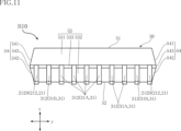
- FIG. 1 is a plan view of a semiconductor device according to a first embodiment of the present disclosure.
- FIG. 2 is a sectional view taken along line II-II in FIG.
- FIG. 3 is a partially enlarged view of FIG. 2.
- FIG. 4 is a cross-sectional view illustrating the manufacturing process of the semiconductor element shown in FIG.
- FIG. 5 is a cross-sectional view illustrating the manufacturing process of the semiconductor element shown in FIG.
- FIG. 6 is a cross-sectional view of a semiconductor element according to a modification of the first embodiment of the present disclosure.
- FIG. 7 is a partially enlarged view of FIG. 6.
- FIG. 8 is a plan view of the semiconductor device according to the first embodiment of the present disclosure.
- FIG. 9 is a plan view corresponding to FIG.
- FIG. 10 is a front view of the semiconductor device shown in FIG. 8.
- 11 is a left side view of the semiconductor device shown in FIG. 8.
- 12 is a right side view of the semiconductor device shown in FIG. 8.
- FIG. 13 is a sectional view taken along line XIII-XIII in FIG. 9.
- FIG. 14 is a cross-sectional view taken along line XIV-XIV in FIG. 9.
- FIG. 15 is a partially enlarged view of FIG. 9.
- FIG. 16 is a cross-sectional view taken along line XVI-XVI in FIG. 15.
- FIG. 17 is a partially enlarged sectional view of the semiconductor device shown in FIG. 8, and the structure of the bonding layer is different from that shown in FIG. 16.
- FIG. 16 is a front view of the semiconductor device shown in FIG. 8.
- 11 is a left side view of the semiconductor device shown in FIG. 8.
- 12 is a right side view of the semiconductor device shown in FIG. 8.
- FIG. 13 is a sectional view taken along line
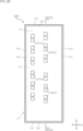
- FIG. 18 is a plan view of a semiconductor device according to a second embodiment of the present disclosure, in which only the outline of the sealing resin is illustrated.
- FIG. 19 is a sectional view taken along line XIX-XIX in FIG. 18.
- FIG. 20 is a plan view of a semiconductor element according to a second embodiment of the present disclosure.
- FIG. 21 is a cross-sectional view taken along line XXI-XXI in FIG. 20.
- FIG. 22 is a partially enlarged view of FIG. 21, showing the second edge of the second side surface and its vicinity.
- FIG. 23 is a partially enlarged view of FIG. 21, showing the first edge of the first side surface and the vicinity thereof.
- FIG. 24 is a cross-sectional view of a semiconductor element according to a modification of the second embodiment of the present disclosure.
- FIG. 25 is a partially enlarged view of FIG. 24.
- FIG. 26 is a plan view of a semiconductor element according to a modification of the third embodiment of the present disclosure.
- FIG. 27 is a cross-sectional view taken along line XXVII-XXVII in FIG. 26.
- semiconductor element A10 A semiconductor device A10 according to a first embodiment of the present disclosure will be described based on FIGS. 1 to 3.
- the semiconductor element A10 includes a main body 11, a plurality of electrodes 12, and a passivation film 13.
- first direction z An example of a direction perpendicular to the first direction z is referred to as a "second direction x.”
- second direction x An example of a direction perpendicular to both the first direction z and the second direction x is referred to as a "third direction y.”
- the semiconductor element A10 transmits electrical signals such as PWM (Pulse Width Modulation) control signals in an insulated state.
- the semiconductor element A10 is of an inductive type.
- An example of the inductive semiconductor element A10 is an insulation type transformer.
- An isolation transformer performs electrical signal transmission in an insulated state by inductively coupling two inductors (coils).
- the two inductors include a transmitting inductor and a receiving inductor. Each of the two inductors is stacked in the first direction z.
- a dielectric layer made of silicon dioxide (SiO 2 ) or the like is located between the transmitting inductor and the receiving inductor.
- the transmitting inductor and the receiving inductor are electrically insulated by the dielectric layer.
- the semiconductor element A10 may be of a capacitive type.
- a capacitor is an example of the capacitive semiconductor element A10.
- the main body portion 11 has a rectangular shape when viewed in the first direction z.
- the dimension of the main body part 11 in the third direction y is larger than the dimension of the main body part 11 in the second direction x. Therefore, when viewed in the first direction z, the main body portion 11 has a rectangular shape with the long side extending in the third direction y.
- Main body portion 11 includes a semiconductor substrate 11A and a semiconductor layer 11B.
- the semiconductor substrate 11A supports the semiconductor layer 11B.
- the composition of the semiconductor substrate 11A includes silicon (Si), for example.
- the semiconductor layer 11B is stacked on the semiconductor substrate 11A.
- the semiconductor layer 11B includes the two inductors described above and the dielectric layer described above. Further, the semiconductor layer 11B includes a rewiring layer that is electrically connected to the two inductors.
- the main body 11 has a main surface 111, a back surface 112, two first side surfaces 113, and two second side surfaces 114.
- the main surface 111 and the back surface 112 face oppositely to each other in the first direction z.
- the two first side surfaces 113 face opposite to each other in the second direction x.
- the two second side surfaces 114 face oppositely to each other in the second direction x.
- the two second side surfaces 114 are individually connected to the two first side surfaces 113.
- Each of the two first side surfaces 113 and the two second side surfaces 114 extends in the third direction y.
- the description of the two first side surfaces 113 and the two second side surfaces 114 will be limited to one of the two first side surfaces 113 and one of the two second side surfaces 114 connected thereto.
- the first side surface 113 has a first edge 113A farthest from the back surface 112.
- the second side surface 114 is connected to the first edge 113A.
- the second side surface 114 is located between the first side surface 113 and the main surface 111 in the first direction z.
- the second side surface 114 overlaps the back surface 112 when viewed in the first direction z.
- the second side surface 114 includes a first region 114A and a second region 114B.
- the first region 114A faces the second direction x.
- the second region 114B is connected to the first edge 113A and the first region 114A.
- the second region 114B is curved toward the back surface 112.
- the dimension h1 of the first side surface 113 in the first direction z is larger than the dimension h2 of the second side surface 114 in the first direction z.
- the dimension h1 is 50% or more of the dimension of the main body portion 11 in the first direction z. Therefore, the dimension h1 is different from the dimension h2.
- the surface roughness of the second side surface 114 is smaller than the surface roughness of the first side surface 113. Therefore, the surface roughness of the first side surface 113 is different from the surface roughness of the second side surface 114. Furthermore, the surface roughness of each of the first side surface 113 and the second side surface 114 is greater than the surface roughness of the back surface 112.
- the second region 114B forms a curved surface with a radius of curvature r1.
- the plurality of electrodes 12 are arranged on the main surface 111 of the main body 11, as shown in FIGS. 1 and 2.
- the plurality of electrodes 12 are electrically connected to a rewiring layer that is a part of the semiconductor layer 11B of the main body portion 11.
- the multiple electrodes 12 include multiple first electrodes 121 and multiple second electrodes 122.
- the plurality of first electrodes 121 are arranged along the third direction y.
- the plurality of second electrodes 122 are located on one side of the plurality of first electrodes 121 in the second direction x.
- the plurality of second electrodes 122 are arranged along the third direction y.
- the composition of the plurality of electrodes 12 includes, for example, aluminum (Al).
- the passivation film 13 is laminated on the main surface 111 of the main body portion 11, as shown in FIG. As shown in FIG. 1, the passivation film 13 surrounds the plurality of electrodes 12 when viewed in the first direction z. Passivation film 13 is an insulator.
- the composition of the passivation film 13 includes, for example, silicon nitride (Si 3 N 4 ).
- a method for forming the first side surface 113 and the second side surface 114 of the main body portion 11 of the semiconductor element A10 will be described based on FIGS. 4 and 5.
- a main body portion 11 including a semiconductor substrate 11A and a semiconductor layer 11B, a plurality of electrodes 12, and a passivation film 13 are formed prior to these formations.
- a tape 80 is attached to the back surface 112 of the main body part 11.
- Tape 80 is a dicing tape.
- a plurality of grooves 83 are formed by removing a portion of each of the main body portion 11 and the passivation film 13 using the first blade 81 having a width b1.
- the width b1 is 25 ⁇ m or more and 40 ⁇ m or less.
- the plurality of grooves 83 are formed from the side facing the main surface 111 of the main body portion 11 toward the back surface 112 in the first direction z.
- the plurality of grooves 83 are formed in a lattice shape along each of the second direction x and the third direction y.
- the main body portion 11 is cut by the second blade 82 having a width b2.
- the width b2 is smaller than the width b1 of the first blade 81.
- the width b2 is 15 ⁇ m or more and 25 ⁇ m or less.
- the surface roughness of the second blade 82 is greater than that of the first blade 81.
- FIGS. 6 and 7 a semiconductor element A11 that is a modification of the semiconductor element A10 will be described.
- the cross-sectional position in FIG. 6 is the same (or substantially the same) as the cross-sectional position in FIG. 2.
- the configurations of the first side surface 113 and the second side surface 114 are different from the configuration of the semiconductor element A10.
- a dimension h2 of the second side surface 114 in the first direction z is larger than a dimension h1 of the first side surface 113 in the first direction z.
- the surface roughness of the second side surface 114 is greater than the surface roughness of the first side surface 113. Also in the semiconductor element A11, when it is assumed that the surface roughness of the second region 114B is 0 (double-dashed line shown in FIG. 7) in a cross section with the first direction z and the second direction x as in-plane directions, The second region 114B forms a curved surface with a radius of curvature r1.
- the semiconductor device B10 includes a control element 61, a driving element 62, a semiconductor element A10, a first die pad 21, a second die pad 22, a bonding layer 29, a plurality of first terminals 31, a plurality of second terminals 32, and a sealing resin 50. Equipped with Further, the semiconductor device B10 includes a plurality of first wires 41, a plurality of second wires 42, a plurality of third wires 43, and a plurality of fourth wires 44.
- the semiconductor device B10 is surface mounted on a wiring board of an inverter device such as an electric vehicle or a hybrid vehicle.
- the package format of the semiconductor device B10 is SOP (Small Outline Package). However, the package format of the semiconductor device B10 is not limited to SOP.
- FIG. 9 shows only the outer shape of the sealing resin 50. In FIG. 9, the outer shape of the sealing resin 50 is shown by an imaginary line (two-dot chain line).
- the control element 61, the drive element 62, and the semiconductor element A10 are elements that serve as the functional center of the semiconductor device B10.
- the control element 61, the drive element 62, and the semiconductor element A10 are composed of individual elements.
- the drive element 62 is located on the opposite side of the control element 61 with respect to the semiconductor element A10 in the second direction x. When viewed in the first direction z, the control element 61 and the drive element 62 have a rectangular shape with the long side extending in the third direction y.
- the control element 61 controls the drive element 62.
- the control element 61 includes a circuit that converts an electrical signal input from another semiconductor device into a PWM control signal, a transmission circuit that transmits the PWM control signal to the drive element 62, and a circuit that converts the electrical signal from the drive element 62. and a receiving circuit for receiving the signal.
- the drive element 62 drives a switching element located outside the semiconductor device B10.
- the switching element is, for example, an IGBT (Insulated Gate Bipolar Transistor) or a MOSFET (Metal-Oxide-Semiconductor Field-Effect Transistor).
- the driving element 62 includes a receiving circuit that receives a PWM control signal, a circuit that drives a switching element based on the PWM control signal, and a transmitting circuit that transmits an electric signal to the control element 61. Examples of the electrical signal include an output signal from a temperature sensor placed near the motor.
- the voltage applied to the control element 61 and the voltage applied to the drive element 62 are relatively different. Therefore, a potential difference is generated between the control element 61 and the drive element 62.
- the voltage applied to the drive element 62 is higher than the voltage applied to the control element 61.
- the power supply voltage supplied to the drive element 62 is higher than the power supply voltage supplied to the control element 61.
- the first circuit including the control element 61 as a component and the second circuit including the drive element 62 as a component are insulated from each other by the semiconductor element A10.
- the semiconductor element A10 is electrically connected to the first circuit and the second circuit.
- the components of the first circuit include a first die pad 21, a plurality of first terminals 31, a plurality of first wires 41, and a plurality of third wires 43, which will be described later.
- the components of the second circuit include a second die pad 22, a plurality of second terminals 32, a plurality of second wires 42, and a plurality of fourth wires 44, which will be described later.
- the first circuit and the second circuit have relatively different potentials.
- the potential of the second circuit is higher than the potential of the first circuit.
- the semiconductor element A10 relays mutual signals in the first circuit and the second circuit.
- the voltage applied to the ground of the control element 61 is approximately 0V, whereas the voltage applied to the ground of the drive element 62 is transiently 600V or more. There is.
- the control element 61 has a plurality of electrodes 611.
- the plurality of electrodes 611 are provided on the upper surface of the control element 61 (a surface facing in the same direction as the first mounting surface 211A of the first pad portion 211 of the first die pad 21 described later).
- the composition of the plurality of electrodes 611 includes, for example, aluminum.
- the plurality of electrodes 611 are electrically connected to a circuit configured in the control element 61.
- the drive element 62 has a plurality of electrodes 621.
- the plurality of electrodes 621 are provided on the upper surface of the drive element 62 (a surface facing in the same direction as a second mounting surface 221A of a second pad portion 221 of a second die pad 22, which will be described later).
- the composition of the plurality of electrodes 621 includes, for example, aluminum.
- the plurality of electrodes 621 are electrically connected to a circuit configured in the drive element 62.
- the semiconductor element A10 is located between the control element 61 and the drive element 62 in the second direction x. Therefore, the control element 61 is located on the opposite side of the drive element 62 with respect to the semiconductor element A10 in the second direction x.
- the plurality of first electrodes 121 of the semiconductor element A10 are located closer to the control element 61 than the drive element 62 in the second direction x.
- the plurality of second electrodes 122 of the semiconductor element A10 are located on the opposite side of the control element 61 with respect to the plurality of first electrodes 121 in the second direction x.
- the first die pad 21, the second die pad 22, the plurality of first terminals 31, and the plurality of second terminals 32 are connected to the control element 61, the drive element 62, the semiconductor element A10, and the wiring board on which the semiconductor device B10 is mounted. Configure a conduction path.
- the first die pad 21, the second die pad 22, the plurality of first terminals 31, and the plurality of second terminals 32 are obtained from the same lead frame.
- the lead frame contains copper in its composition.
- the first die pad 21 and the second die pad 22 are separated from each other in the second direction x, as shown in FIGS. 8 and 9.
- the control element 61 is mounted on the first die pad 21, and the drive element 62 is mounted on the second die pad 22.
- the voltage applied to the second die pad 22 is relatively different from the voltage applied to the first die pad 21.
- the voltage applied to the second die pad 22 is higher than the voltage applied to the first die pad 21.
- the first die pad 21 has a first pad part 211 and two first hanging lead parts 212.
- the control element 61 is mounted on the first pad section 211.
- the first pad portion 211 has a first mounting surface 211A facing in the first direction z.
- the control element 61 is bonded to the first mounting surface 211A via the bonding layer 29.
- the bonding layer 29 is made of a paste containing metal particles.
- the composition of the metal particles is, for example, silver (Ag). Therefore, bonding layer 29 is a conductor. In addition, the bonding layer 29 may be solder.
- the first pad portion 211 is covered with a sealing resin 50.
- the thickness of the first pad portion 211 is, for example, 150 ⁇ m or more and 200 ⁇ m or less.
- the back surface 112 of the main body 11 of the semiconductor element A10 faces the first mounting surface 211A of the first die pad 21.
- the main body portion 11 is bonded to the first mounting surface 211A via the bonding layer 29.
- the bonding layer 29 is in contact with the first side surface 113 of the main body portion 11 .
- the bonding layer 29 reaches the first edge 113A of the first side surface 113. That is, the bonding layer 29 is also in contact with the first edge 113A.
- the bonding layer 29 may be in contact with the first side surface 113 and the second side surface 114 of the main body portion 11. In this case, the bonding layer 29 straddles the first edge 113A of the first side surface 113.
- a plurality of through holes 213 are formed in the first pad portion 211.
- Each of the plurality of through holes 213 penetrates the first pad portion 211 in the first direction z and extends in the third direction y.
- at least one of the plurality of through holes 213 is located between the control element 61 and the semiconductor element A10.
- the plurality of through holes 213 are arranged along the third direction y.
- the two first hanging lead parts 212 are connected to both sides of the first pad part 211 in the third direction y.
- the two first hanging lead parts 212 have a covering part 212A and an exposed part 212B.
- the covering portion 212A is connected to the first pad portion 211 and is covered with the sealing resin 50.
- the covering portion 212A includes a section extending in the second direction x.
- the exposed portion 212B is connected to the covering portion 212A and exposed from the sealing resin 50. When viewed in the first direction z, the exposed portion 212B extends in the second direction x.
- the exposed portion 212B is bent in a gullwing shape when viewed in the third direction y.
- tin (Sn) plating may be applied to the surface of the exposed portion 212B.
- the second die pad 22 has a second pad part 221 and two second hanging lead parts 222.
- the drive element 62 is mounted on the second pad section 221.
- the second pad portion 221 has a second mounting surface 221A facing in the first direction z.
- the drive element 62 is bonded to the second mounting surface 221A via the bonding layer 29.
- the second pad portion 221 is covered with a sealing resin 50.
- the thickness of the second pad portion 221 is, for example, 150 ⁇ m or more and 200 ⁇ m or less.
- the area of the second pad portion 221 is smaller than the area of the first pad portion 211 of the first die pad 21 .
- the second pad section 221 overlaps the first pad section 211 when viewed in the second direction x.
- the two second hanging lead parts 222 extend from both sides of the second pad part 221 in the third direction y.
- the two second hanging lead parts 222 have a covering part 222A and an exposed part 222B.
- the covering portion 222A is connected to the second pad portion 221 and covered with the sealing resin 50.
- the covering portion 222A includes a section extending in the second direction x.
- the exposed portion 222B is connected to the covering portion 222A and exposed from the sealing resin 50.
- the exposed portion 222B extends in the second direction x.
- the exposed portion 222B is bent in a gull wing shape when viewed in the third direction y.
- tin plating may be applied to the surface of the exposed portion 222B.
- the plurality of first terminals 31 are located on the opposite side of the drive element 62 with respect to the semiconductor element A10 in the second direction x.
- the plurality of first terminals 31 are arranged along the third direction y. At least one of the plurality of first terminals 31 is electrically connected to the control element 61 via the third wire 43.
- the plurality of first terminals 31 are located between the two first hanging lead parts 212 of the first die pad 21 in the third direction y.
- the plurality of first terminals 31 include a plurality of first intermediate terminals 31A and two first side terminals 31B.
- the two first side terminals 31B are located on both sides of the plurality of first intermediate terminals 31A in the third direction y.
- the plurality of first terminals 31 have a covering portion 311 and an exposed portion 312.
- the covering portion 311 is covered with a sealing resin 50.
- the dimension of the covering portion 311 of each of the two first side terminals 31B in the second direction x is larger than the dimension of the covering portion 311 of each of the plurality of first intermediate terminals 31A in the second direction x.
- the exposed portion 312 is connected to the covering portion 311 and exposed from the sealing resin 50.
- the exposed portion 312 extends in the second direction x.
- the exposed portion 312 is bent in a gullwing shape.
- the shape of the exposed portion 312 is equal to the shape of the exposed portion 212B of each of the two first hanging lead portions 212 of the first die pad 21.
- the surface of the exposed portion 312 may be plated with tin, for example.
- the plurality of second terminals 32 are located on the opposite side of the control element 61 with respect to the semiconductor element A10 in the second direction x.
- the plurality of second terminals 32 are arranged along the third direction y. At least one of the plurality of second terminals 32 is electrically connected to the drive element 62 via the fourth wire 44.
- the plurality of second terminals 32 include a plurality of second intermediate terminals 32A and two second side terminals 32B.
- Two second hanging lead parts 222 of the second die pad 22 are located on both sides of the plurality of second intermediate terminals 32A in the third direction y.
- the two second side terminals 32B are located so as to sandwich the plurality of second intermediate terminals 32A and the two second hanging lead parts 222 in between in the third direction y.
- the plurality of second terminals 32 have a covering portion 321 and an exposed portion 322.
- the covering portion 321 is covered with a sealing resin 50.
- the dimension of the covering portion 321 of each of the two second side terminals 32B in the second direction x is larger than the dimension of the covering portion 321 of each of the plurality of second intermediate terminals 32A in the second direction x.
- the exposed portion 322 is connected to the covering portion 321 and exposed from the sealing resin 50. When viewed in the first direction z, the exposed portion 322 extends in the second direction x. As shown in FIG. 10, the exposed portion 322 is bent in a gullwing shape when viewed in the third direction y. The shape of the exposed portion 322 is equal to the shape of the exposed portion 222B of each of the two second hanging lead portions 222 of the second die pad 22.
- the surface of the exposed portion 322 may be plated with tin, for example.
- the plurality of first wires 41, the plurality of second wires 42, the plurality of third wires 43, and the plurality of fourth wires 44 are connected to the first die pad 21, the second die pad 22, the plurality of first terminals 31, and the plurality of Together with the second terminal 32, the control element 61, the drive element 62, and the semiconductor element A10 constitute a conduction path for performing a predetermined function.
- the plurality of first wires 41 are electrically connected to the plurality of first electrodes 121 of the semiconductor element A10 and the plurality of electrodes 611 of the control element 61, as shown in FIGS. 9 and 13. Thereby, the control element 61 and the semiconductor element A10 are electrically connected to each other.
- the plurality of first wires 41 are arranged along the third direction y.
- the composition of the plurality of first wires 41 includes gold (Au).
- the plurality of second wires 42 are electrically connected to the plurality of second electrodes 122 of the semiconductor element A10 and the plurality of electrodes 621 of the drive element 62, as shown in FIGS. 9 and 13. Thereby, the drive element 62 and the semiconductor element A10 are electrically connected to each other.
- the plurality of second wires 42 are arranged along the third direction y. In the semiconductor device B ⁇ b>10 , the plurality of second wires 42 straddle between the first pad portion 211 of the first die pad 21 and the second pad portion 221 of the second die pad 22 .
- the composition of the plurality of second wires 42 includes gold.
- the plurality of third wires 43 are electrically connected to the plurality of electrodes 611 of the control element 61 and the covering portions 311 of the plurality of first terminals 31, as shown in FIGS. 9 and 13. Thereby, at least one of the plurality of first terminals 31 is electrically connected to the control element 61. Furthermore, at least one of the plurality of third wires 43 is conductively bonded to one of the plurality of electrodes 611 and one of the covering parts 212A of the two first hanging lead parts 212 of the first die pad 21. As a result, at least one of the two first suspension lead portions 212 is electrically connected to the control element 61. As a result, at least one of the two first suspension lead portions 212 serves as a ground terminal of the control element 61.
- the composition of the plurality of third wires 43 includes gold.
- the composition of the plurality of first wires 41 may include copper.
- the plurality of fourth wires 44 are electrically connected to the plurality of electrodes 621 of the drive element 62 and the covering portions 321 of the plurality of second terminals 32, as shown in FIGS. 9 and 13. Thereby, at least one of the plurality of second terminals 32 is electrically connected to the drive element 62. Further, at least one of the plurality of fourth wires 44 is electrically conductively bonded to one of the plurality of electrodes 621 and one of the covering parts 222A of the two second hanging lead parts 222 of the second die pad 22. As a result, at least one of the two second suspension lead portions 222 is electrically connected to the drive element 62. As a result, at least one of the two second suspension lead portions 222 serves as a ground terminal of the drive element 62.
- the composition of the plurality of fourth wires 44 includes gold. In addition, the composition of the plurality of fourth wires 44 may include copper.
- the plurality of first wires 41 straddle one of the two first side surfaces 113 of the main body section 11 and one of the two second side surfaces 114 of the main body section 11 connected thereto.
- the plurality of second wires 42 straddle the other of the two first side surfaces 113 and the other of the two second side surfaces 114 connected thereto.
- the sealing resin 50 includes a control element 61, a driving element 62, a semiconductor element A10, a first die pad 21, a second die pad 22, a plurality of first terminals 31, and a plurality of second terminals 32. covering at least a portion of each of the above. Furthermore, the sealing resin 50 covers the plurality of first wires 41 , the plurality of second wires 42 , the plurality of third wires 43 , and the plurality of fourth wires 44 .
- the sealing resin 50 is an insulator.
- the sealing resin 50 is made of a material containing, for example, epoxy resin.
- the sealing resin 50 has a rectangular shape when viewed in the first direction z.
- the sealing resin 50 has a top surface 51, a bottom surface 52, two first side surfaces 53, and two second side surfaces 54.
- the top surface 51 and the bottom surface 52 are located apart from each other in the first direction z.
- the top surface 51 and the bottom surface 52 face oppositely to each other in the first direction z.
- Each of the top surface 51 and the bottom surface 52 is substantially flat.
- the two first side surfaces 53 are connected to the top surface 51 and the bottom surface 52, and are located apart from each other in the second direction x. From the first side surface 53 located on one side in the second direction x among the two first side surfaces 53, the exposed portions 212B of the two first hanging lead portions 212 of the first die pad 21 and the plurality of first terminals 31 are exposed. The exposed portion 312 is exposed. From the first side surface 53 located on the other side in the second direction x of the two first side surfaces 53, the exposed portions 212B of the two second hanging lead portions 222 of the second die pad 22 and the plurality of second terminals 32 are exposed. The exposed portion 322 is exposed.
- each of the two first side surfaces 53 includes a first upper portion 531, a first lower portion 532, and a first intermediate portion 533.
- the first upper portion 531 is connected to the top surface 51 on one side in the first direction z, and connected to the first intermediate portion 533 on the other side in the first direction z.
- the first upper portion 531 is inclined with respect to the top surface 51.
- the first lower portion 532 is connected to the bottom surface 52 on one side in the first direction z, and connected to the first intermediate portion 533 on the other side in the first direction z.
- the first lower portion 532 is inclined with respect to the bottom surface 52.
- the first intermediate portion 533 is connected to the first upper portion 531 on one side in the first direction z, and connected to the first lower portion 532 on the other side in the first direction z.
- the in-plane directions of the first intermediate portion 533 are the first direction z and the third direction y.
- the first intermediate portion 533 is located outward from the top surface 51 and the bottom surface 52. From the first intermediate portions 533 of the two first side surfaces 53, the exposed portions 212B of the two first hanging lead portions 212 of the first die pad 21 and the exposed portions 212B of the two second hanging lead portions 222 of the second die pad 22.
- the exposed portions 312 of the plurality of first terminals 31 and the exposed portions 322 of the plurality of second terminals 32 are exposed.
- the two second side surfaces 54 are connected to the top surface 51 and the bottom surface 52, and are located apart from each other in the third direction y.
- the first die pad 21, the second die pad 22, the plurality of first terminals 31, and the plurality of second terminals 32 are located apart from the two second side surfaces 54.
- each of the two second side surfaces 54 includes a second upper portion 541, a second lower portion 542, and a second intermediate portion 543.
- the second upper portion 541 is connected to the top surface 51 on one side in the first direction z, and connected to the second intermediate portion 543 on the other side in the first direction z.
- the second upper portion 541 is inclined with respect to the top surface 51.
- the second lower portion 542 is connected to the bottom surface 52 on one side in the first direction z, and connected to the second intermediate portion 543 on the other side in the first direction z.
- the second lower portion 542 is inclined with respect to the bottom surface 52.
- the second intermediate portion 543 is connected to the second upper portion 541 on one side in the first direction z, and connected to the second lower portion 542 on the other side in the first direction z.
- the in-plane directions of the second intermediate portion 543 are the first direction z and the third direction y.
- the second intermediate portion 543 is located outward from the top surface 51 and the bottom surface 52 when viewed in the first direction z.
- a half-bridge circuit including a low side (low potential side) switching element and a high side (high potential side) switching element is generally configured.
- the following description deals with the case where these switching elements are MOSFETs.
- the reference potentials of the source of the switching element and the gate driver that drives the switching element are both ground.
- the reference potentials of the source of the switching element and the gate driver that drives the switching element both correspond to the potential at the output node of the half-bridge circuit.
- the reference potential of the gate driver that drives the high-side switching element changes.
- the reference potential is equivalent to the voltage applied to the drain of the high-side switching element (for example, 600 V or more).
- the ground of the control element 61 and the ground of the drive element 62 are configured to be separated. Therefore, when the semiconductor device B10 is used as a gate driver for driving a high-side switching element, a voltage equivalent to the voltage applied to the drain of the high-side switching element is transiently applied to the ground of the driving element 62. applied.
- FIG. 18 shows only the outer shape of the sealing resin 50.
- the outer shape of the sealing resin 50 is shown with imaginary lines.
- the configuration of the semiconductor element A10 is different from the configuration of the semiconductor device B10.
- the semiconductor element A10 is bonded to the second mounting surface 221A of the second pad portion 221 of the second die pad 22. Similar to the semiconductor device B10, the main body portion 11 of the semiconductor element A10 is bonded to the second mounting surface 221A via the bonding layer 29. In the semiconductor device B20 as well, the bonding layer 29 is in contact with the first side surface 113 of the main body portion 11. Therefore, in the semiconductor device B20, the plurality of first wires 41 span between the first pad section 211 of the first die pad 21 and the second pad section 221. In this way, even if the potential of the second pad section 221 is higher than the potential of the first pad section 211, the semiconductor element A10 can be mounted on the second pad section 221.
- the main body portion 11 of the semiconductor element A10 has a first side surface 113 facing in the second direction x, and a second side surface 114 connected to the first edge 113A of the first side surface 113.
- the second side surface 114 is located between the first side surface 113 and the main surface 111 of the main body portion 11 in the first direction z.
- the second side surface 114 overlaps the back surface 112 of the main body portion 11 when viewed in the first direction z.
- the surface tension of the bonding layer 29 at the first edge 113A makes it difficult for the bonding layer 29 to creep up to the side where the main surface 111 is located rather than the first edge 113A.
- the surface roughness of the first side surface 113 is different from the surface roughness of the second side surface 114.
- creeping of the bonding layer 29 against the semiconductor element A10 can be efficiently controlled.
- the bonding layer 29 is formed on the first side surface 113 before the bonding layer 29 reaches the first edge 113A. You can stop the creeping up.
- the surface roughness of the second side surface 114 is larger than the surface roughness of the first side surface 113 as in the semiconductor element A11, as shown in FIG. You can stop the creeping. Therefore, according to the above-mentioned configuration and the present configuration, it is possible to suppress the rising of the bonding layer 29 in the semiconductor element A10.
- the surface roughness of the second side surface 114 is smaller than the surface roughness of the first side surface 113, in order to reliably stop the creeping up of the bonding layer 29 on the first side surface 113, the surface roughness of the first side surface 113 in the first direction z is It is preferable that the dimension h1 is larger than the dimension h2 of the second side surface 114 in the first direction z.
- the surface roughness of the first blade 81 shown in FIG. 4 is set to be smaller than the surface roughness of the second blade 82 shown in FIG. It is possible to prevent defects from occurring on the main surface 111 of the main body portion 11.
- the second side surface 114 is It is preferable that the dimension h2 is larger than the dimension h1 of the first side surface 113 in the first direction z.
- the plurality of first wires 41 and the plurality of second wires 42 straddle the first side surface 113 and the second side surface 114.
- each of the first die pad 21, the second die pad 22, the plurality of first terminals 31, and the plurality of second terminals 32 is located on either of the two first side surfaces 53 of the sealing resin 50. It is exposed from the top.
- the two first hanging lead parts 212 of the first die pad 21 are exposed from one side of the sealing resin 50 in the second direction x, and the two second hanging lead parts 222 of the second die pad 22 are sealed. This is obtained by exposing the stopper resin 50 from the other side in the second direction x.
- the first die pad 21, the second die pad 22, the plurality of first terminals 31, and the plurality of second terminals 32 are located apart from the two second side surfaces 54 of the sealing resin 50.
- the first die pad 21, the second die pad 22, the plurality of first terminals 31, and the plurality of second terminals 32 are all not exposed from the two second side surfaces 54. This configuration contributes to improving the dielectric strength of the semiconductor device B10.
- a plurality of through holes 213 are formed in the first pad portion 211 of the first die pad 21, which has a larger area than the second pad portion 221 of the second die pad 22.
- semiconductor element A20 A semiconductor element A20 according to a second embodiment of the present disclosure will be described based on FIGS. 20 to 23.
- the same or similar elements as those of the semiconductor element A10 described above are given the same reference numerals, and redundant explanation will be omitted.
- the configuration of the main body portion 11 is different from the configuration of the semiconductor device A10.
- the main body portion 11 has two third side surfaces 115.
- the two third side surfaces 115 face oppositely to each other in the second direction x.
- the two third side surfaces 115 are individually connected to the two second side surfaces 114.
- Each of the two third side surfaces 115 extends in the third direction y.
- the description of the two third side surfaces 115 will be limited to either one of the two third side surfaces 115 connected to either of the two second side surfaces 114.
- the second side surface 114 has a second edge 114C that is farthest from the back surface 112.
- the third side surface 115 is connected to the second edge 114C.
- the third side surface 115 is located between the second side surface 114 and the main surface 111 of the main body portion 11 in the first direction z.
- the third side surface 115 overlaps the back surface 112 of the main body portion 11 when viewed in the first direction z.
- the third side surface 115 includes a third region 115A.
- the third region 115A is connected to the second edge 114C.
- the third region 115A is curved toward the back surface 112 of the main body portion 11.
- the dimension h1 of the first side surface 113 in the first direction z is smaller than the dimension h2 of the second side surface 114 in the first direction z.
- the dimension h3 of the third side surface 115 in the first direction z is smaller than the dimension h2.
- the surface roughness of the third side surface 115 is smaller than the surface roughness of the second side surface 114.
- the surface roughness of the third side surface 115 is greater than that of the back surface 112.
- the surface roughness of the second side surface 114 is greater than the surface roughness of the first side surface 113.
- the third region 115A forms a curved surface with a radius of curvature r2.
- the radius of curvature r2 is larger than the radius of curvature r1 shown in FIG.
- semiconductor element A21 Next, as shown in FIGS. 24 and 25, a semiconductor element A21, which is a modification of the semiconductor element A20, will be described.
- the cross-sectional position in FIG. 24 is the same (or substantially the same) as the cross-sectional position in FIG. 21.
- the configurations of the second side surface 114 and the third side surface 115 are different from the configuration of the semiconductor element A20.
- a dimension h3 of the third side surface 115 in the first direction z is larger than a dimension h2 of the second side surface 114 in the first direction z.
- the surface roughness of the third side surface 115 is greater than the surface roughness of the second side surface 114. Also in the semiconductor element A21, when it is assumed that the surface roughness of the third region 115A is 0 (double-dashed line shown in FIG. 25) in a cross section with the first direction z and the second direction x as in-plane directions, The third region 115A forms a curved surface with a radius of curvature r2.
- the main body portion 11 of the semiconductor element A20 has a first side surface 113 facing in the second direction x, and a second side surface 114 connected to the first edge 113A of the first side surface 113.
- the second side surface 114 is located between the first side surface 113 and the main surface 111 of the main body portion 11 in the first direction z.
- the second side surface 114 overlaps the back surface 112 of the main body portion 11 when viewed in the first direction z.
- the surface roughness of the first side surface 113 is different from the surface roughness of the second side surface 114. Therefore, according to this configuration, it is possible to suppress the rising of the bonding layer 29 also in the semiconductor element A20.
- the semiconductor element A20 has the same configuration as the semiconductor element A10, so that the same effect as that of the semiconductor element A10 can be achieved.
- the main body portion 11 has a third side surface 115 connected to the second edge 114C of the second side surface 114.
- the third side surface 115 is located between the second side surface 114 and the main surface 111 of the main body portion 11 in the first direction z.
- the third side surface 115 overlaps the back surface 112 of the main body portion 11 when viewed in the first direction z.
- semiconductor element A30 A semiconductor element A30 according to a third embodiment of the present disclosure will be described based on FIGS. 26 and 27.
- the same or similar elements as those of the semiconductor element A10 described above are given the same reference numerals, and redundant explanation will be omitted.
- the configuration of the main body portion 11 is different from the configuration of the semiconductor device A10.
- the main body portion 11 has two fourth side surfaces 116 and two fifth side surfaces 117.
- the two fourth side surfaces 116 face oppositely to each other in the third direction y.
- the two fifth side surfaces 117 face oppositely to each other in the third direction y.
- the two fifth side surfaces 117 are individually connected to the two fourth side surfaces 116.
- Each of the two fourth side surfaces 116 and the two fifth side surfaces 117 extends in the third direction y.
- each of the two fourth side surfaces 116 has a third edge 116A furthest from the back surface 112.
- the two fifth side surfaces 117 are individually connected to the third edges 116A of the two fourth side surfaces 116.
- the two fifth side surfaces 117 are located between the two fourth side surfaces 116 and the main surface 111 of the main body portion 11 in the first direction z.
- the two fifth side surfaces 117 overlap the back surface 112 of the main body 11 when viewed in the first direction z.
- the dimension h4 in the first direction z of each of the two fourth side surfaces 116 is equal to the dimension h1 in the first direction z of the first side surface 113 shown in FIG. h5 in the first direction z of each of the two fifth side surfaces 117 is equal to h2 in the first direction z of the second side surface 114 shown in FIG. Therefore, dimension h4 is larger than dimension h5.
- the main body section 11 has two first side surfaces 113, two second side surfaces 114, two fourth side surfaces 116, and two fifth side surfaces 117, the periphery of the main surface 111 of the main body section 11 It is surrounded by the back surface 112 of.
- the main body portion 11 of the semiconductor element A30 has a first side surface 113 facing in the second direction x, and a second side surface 114 connected to the first edge 113A of the first side surface 113.
- the second side surface 114 is located between the first side surface 113 and the main surface 111 of the main body portion 11 in the first direction z.
- the second side surface 114 overlaps the back surface 112 of the main body portion 11 when viewed in the first direction z.
- the surface roughness of the first side surface 113 is different from the surface roughness of the second side surface 114. Therefore, according to this configuration, it is possible to suppress the rising of the bonding layer 29 also in the semiconductor element A30.
- the semiconductor element A30 has the same configuration as the semiconductor element A10, so that it can achieve the same effects as the semiconductor element A10.
- a main body portion having a main surface and a back surface facing oppositely to each other in the first direction; a plurality of electrodes arranged on the main surface and electrically connected to the main body,
- the main body portion has a first side surface facing in a second direction perpendicular to the first direction,
- the first side surface includes a first edge furthest from the back surface,
- the main body portion has a second side surface connected to the first edge and located between the first side surface and the main surface in the first direction, When viewed in the first direction, the second side surface overlaps the back surface,
- a semiconductor device wherein the first side surface has a surface roughness different from that of the second side surface.
- the dimension of the first side surface in the first direction is larger than the dimension of the second side surface in the first direction,
- Appendix 3. The semiconductor device according to appendix 2, wherein a dimension of the first side surface in the first direction is 50% or more of a dimension of the main body portion in the first direction.
- Appendix 4. The dimension of the second side surface in the first direction is larger than the dimension of the first side surface in the first direction, The semiconductor device according to appendix 1, wherein the second side surface has a surface roughness greater than the first side surface.
- the second side surface includes a first region facing the second direction, and a second region connected to the first edge and the first region, 5.
- the semiconductor device according to any one of appendices 1 to 4, wherein the second region is curved toward the back surface.
- the second side surface includes a second edge furthest from the back surface,
- the main body portion has a third side surface connected to the second edge and located between the second side surface and the main surface in the first direction,
- the semiconductor device according to any one of appendices 1 to 5, wherein the third side surface overlaps the back surface when viewed in the first direction.
- Appendix 7 The dimension of the second side surface in the first direction is larger than the dimension of the third side surface in the first direction,
- the semiconductor device according to appendix 6, wherein the third side surface has a smaller surface roughness than the second side surface.
- the dimension of the third side surface in the first direction is larger than the dimension of the second side surface in the first direction
- Appendix 9. The semiconductor device according to any one of appendices 1 to 8, wherein the main surface is surrounded by a periphery of the back surface when viewed in the first direction.
- Appendix 10. The semiconductor according to any one of Supplementary Notes 1 to 9, wherein a dimension of the main body in a third direction perpendicular to the first direction and the second direction is larger than a dimension of the main body in the second direction. element. Appendix 11.
- a semiconductor device according to any one of Supplementary Notes 1 to 10, a first die pad facing the back surface; a bonding layer bonding the first die pad and the semiconductor element; a plurality of wires individually conductively bonded to the plurality of electrodes, The plurality of wires straddle the first side surface and the second side surface, The semiconductor device, wherein the bonding layer is in contact with the first side surface. Appendix 12. The semiconductor device according to appendix 11, wherein the bonding layer is in contact with the first edge. Appendix 13.
- the plurality of electrodes include a plurality of first electrodes and a plurality of second electrodes
- the plurality of wires include a plurality of first wires individually conductively joined to the plurality of first electrodes, and a plurality of second wires individually conductively joined to the plurality of second electrodes,
- the plurality of first wires are electrically conductively bonded to the drive element, 13.
- the control element is mounted on the first die pad, The semiconductor device according to appendix 13, wherein the drive element is mounted on the second die pad. Appendix 15. The semiconductor device according to appendix 14, wherein the control element is located on the opposite side of the drive element with respect to the semiconductor element in the second direction. Appendix 16. 16. The semiconductor device according to any one of appendices 13 to 15, further comprising a sealing resin that covers the semiconductor element, the control element, the drive element, and the plurality of wires. Appendix 17.
Landscapes
- Structures Or Materials For Encapsulating Or Coating Semiconductor Devices Or Solid State Devices (AREA)
- Engineering & Computer Science (AREA)
- Power Engineering (AREA)
Priority Applications (2)
| Application Number | Priority Date | Filing Date | Title |
|---|---|---|---|
| JP2024507659A JPWO2023176370A1 (https=) | 2022-03-17 | 2023-02-24 | |
| US18/883,501 US20250006775A1 (en) | 2022-03-17 | 2024-09-12 | Semiconductor element and semiconductor device |
Applications Claiming Priority (2)
| Application Number | Priority Date | Filing Date | Title |
|---|---|---|---|
| JP2022042701 | 2022-03-17 | ||
| JP2022-042701 | 2022-03-17 |
Related Child Applications (1)
| Application Number | Title | Priority Date | Filing Date |
|---|---|---|---|
| US18/883,501 Continuation US20250006775A1 (en) | 2022-03-17 | 2024-09-12 | Semiconductor element and semiconductor device |
Publications (1)
| Publication Number | Publication Date |
|---|---|
| WO2023176370A1 true WO2023176370A1 (ja) | 2023-09-21 |
Family
ID=88023448
Family Applications (1)
| Application Number | Title | Priority Date | Filing Date |
|---|---|---|---|
| PCT/JP2023/006742 Ceased WO2023176370A1 (ja) | 2022-03-17 | 2023-02-24 | 半導体素子および半導体装置 |
Country Status (3)
| Country | Link |
|---|---|
| US (1) | US20250006775A1 (https=) |
| JP (1) | JPWO2023176370A1 (https=) |
| WO (1) | WO2023176370A1 (https=) |
Citations (6)
| Publication number | Priority date | Publication date | Assignee | Title |
|---|---|---|---|---|
| JP2014090117A (ja) * | 2012-10-31 | 2014-05-15 | Rohm Co Ltd | 半導体装置、半導体装置の実装構造、および半導体装置の製造方法 |
| WO2014167745A1 (ja) * | 2013-04-10 | 2014-10-16 | 三菱電機株式会社 | 半導体装置、半導体装置の製造方法 |
| JP2016207714A (ja) * | 2015-04-16 | 2016-12-08 | ローム株式会社 | 半導体装置 |
| JP2017135295A (ja) * | 2016-01-29 | 2017-08-03 | サンケン電気株式会社 | 半導体素子 |
| JP2018157168A (ja) * | 2017-03-21 | 2018-10-04 | 東芝メモリ株式会社 | 半導体装置及びその製造方法 |
| WO2019163941A1 (ja) * | 2018-02-22 | 2019-08-29 | 京セラ株式会社 | パワーモジュール用基板およびパワーモジュール |
-
2023
- 2023-02-24 WO PCT/JP2023/006742 patent/WO2023176370A1/ja not_active Ceased
- 2023-02-24 JP JP2024507659A patent/JPWO2023176370A1/ja active Pending
-
2024
- 2024-09-12 US US18/883,501 patent/US20250006775A1/en active Pending
Patent Citations (6)
| Publication number | Priority date | Publication date | Assignee | Title |
|---|---|---|---|---|
| JP2014090117A (ja) * | 2012-10-31 | 2014-05-15 | Rohm Co Ltd | 半導体装置、半導体装置の実装構造、および半導体装置の製造方法 |
| WO2014167745A1 (ja) * | 2013-04-10 | 2014-10-16 | 三菱電機株式会社 | 半導体装置、半導体装置の製造方法 |
| JP2016207714A (ja) * | 2015-04-16 | 2016-12-08 | ローム株式会社 | 半導体装置 |
| JP2017135295A (ja) * | 2016-01-29 | 2017-08-03 | サンケン電気株式会社 | 半導体素子 |
| JP2018157168A (ja) * | 2017-03-21 | 2018-10-04 | 東芝メモリ株式会社 | 半導体装置及びその製造方法 |
| WO2019163941A1 (ja) * | 2018-02-22 | 2019-08-29 | 京セラ株式会社 | パワーモジュール用基板およびパワーモジュール |
Also Published As
| Publication number | Publication date |
|---|---|
| US20250006775A1 (en) | 2025-01-02 |
| JPWO2023176370A1 (https=) | 2023-09-21 |
Similar Documents
| Publication | Publication Date | Title |
|---|---|---|
| JP7792472B2 (ja) | 半導体装置 | |
| WO2022202129A1 (ja) | 半導体装置 | |
| US20240047438A1 (en) | Semiconductor equipment | |
| WO2023112677A1 (ja) | 半導体装置および半導体装置の製造方法 | |
| US20230307424A1 (en) | Semiconductor device | |
| US20240312877A1 (en) | Semiconductor device | |
| JP7798800B2 (ja) | 半導体装置 | |
| JP7843276B2 (ja) | 半導体装置 | |
| WO2023176370A1 (ja) | 半導体素子および半導体装置 | |
| JP7837876B2 (ja) | 半導体装置 | |
| JP7791168B2 (ja) | 半導体装置 | |
| WO2023223843A1 (ja) | 半導体装置 | |
| US20240030109A1 (en) | Semiconductor device | |
| US20250309068A1 (en) | Semiconductor device | |
| WO2024202966A1 (ja) | 半導体装置 | |
| US20260096448A1 (en) | Semiconductor device | |
| WO2024257543A1 (ja) | 半導体装置 | |
| JP2025145876A (ja) | 半導体装置 | |
| WO2025069992A1 (ja) | 半導体装置 | |
| WO2022176690A1 (ja) | 半導体装置、半導体装置の設計方法および半導体装置の製造方法 | |
| WO2025216041A1 (ja) | 半導体装置およびインバータシステム | |
| JP2025130771A (ja) | 半導体装置 | |
| JP2025121430A (ja) | 半導体装置、半導体装置の設計方法および半導体装置の製造方法 | |
| WO2025177840A1 (ja) | 半導体装置および車両 |
Legal Events
| Date | Code | Title | Description |
|---|---|---|---|
| 121 | Ep: the epo has been informed by wipo that ep was designated in this application |
Ref document number: 23770329 Country of ref document: EP Kind code of ref document: A1 |
|
| ENP | Entry into the national phase |
Ref document number: 2024507659 Country of ref document: JP Kind code of ref document: A |
|
| NENP | Non-entry into the national phase |
Ref country code: DE |
|
| 122 | Ep: pct application non-entry in european phase |
Ref document number: 23770329 Country of ref document: EP Kind code of ref document: A1 |