WO2023176037A1 - 光学部材及び光学装置 - Google Patents
光学部材及び光学装置 Download PDFInfo
- Publication number
- WO2023176037A1 WO2023176037A1 PCT/JP2022/040455 JP2022040455W WO2023176037A1 WO 2023176037 A1 WO2023176037 A1 WO 2023176037A1 JP 2022040455 W JP2022040455 W JP 2022040455W WO 2023176037 A1 WO2023176037 A1 WO 2023176037A1
- Authority
- WO
- WIPO (PCT)
- Prior art keywords
- optical
- light
- fillers
- optical member
- optical element
- Prior art date
- Legal status (The legal status is an assumption and is not a legal conclusion. Google has not performed a legal analysis and makes no representation as to the accuracy of the status listed.)
- Ceased
Links
Images




Classifications
-
- G—PHYSICS
- G02—OPTICS
- G02B—OPTICAL ELEMENTS, SYSTEMS OR APPARATUS
- G02B6/00—Light guides; Structural details of arrangements comprising light guides and other optical elements, e.g. couplings
- G02B6/24—Coupling light guides
- G02B6/26—Optical coupling means
- G02B6/262—Optical details of coupling light into, or out of, or between fibre ends, e.g. special fibre end shapes or associated optical elements
-
- G—PHYSICS
- G02—OPTICS
- G02B—OPTICAL ELEMENTS, SYSTEMS OR APPARATUS
- G02B6/00—Light guides; Structural details of arrangements comprising light guides and other optical elements, e.g. couplings
- G02B6/24—Coupling light guides
- G02B6/26—Optical coupling means
-
- G—PHYSICS
- G02—OPTICS
- G02B—OPTICAL ELEMENTS, SYSTEMS OR APPARATUS
- G02B6/00—Light guides; Structural details of arrangements comprising light guides and other optical elements, e.g. couplings
- G02B6/24—Coupling light guides
- G02B6/26—Optical coupling means
- G02B6/32—Optical coupling means having lens focusing means positioned between opposed fibre ends
-
- G—PHYSICS
- G02—OPTICS
- G02B—OPTICAL ELEMENTS, SYSTEMS OR APPARATUS
- G02B6/00—Light guides; Structural details of arrangements comprising light guides and other optical elements, e.g. couplings
- G02B6/24—Coupling light guides
- G02B6/26—Optical coupling means
- G02B6/34—Optical coupling means utilising prism or grating
-
- G—PHYSICS
- G02—OPTICS
- G02B—OPTICAL ELEMENTS, SYSTEMS OR APPARATUS
- G02B6/00—Light guides; Structural details of arrangements comprising light guides and other optical elements, e.g. couplings
- G02B6/24—Coupling light guides
- G02B6/42—Coupling light guides with opto-electronic elements
-
- G—PHYSICS
- G02—OPTICS
- G02B—OPTICAL ELEMENTS, SYSTEMS OR APPARATUS
- G02B6/00—Light guides; Structural details of arrangements comprising light guides and other optical elements, e.g. couplings
- G02B6/24—Coupling light guides
- G02B6/42—Coupling light guides with opto-electronic elements
- G02B6/4201—Packages, e.g. shape, construction, internal or external details
- G02B6/4204—Packages, e.g. shape, construction, internal or external details the coupling comprising intermediate optical elements, e.g. lenses, holograms
- G02B6/4206—Optical features
-
- G—PHYSICS
- G02—OPTICS
- G02B—OPTICAL ELEMENTS, SYSTEMS OR APPARATUS
- G02B6/00—Light guides; Structural details of arrangements comprising light guides and other optical elements, e.g. couplings
- G02B6/24—Coupling light guides
- G02B6/42—Coupling light guides with opto-electronic elements
- G02B6/4201—Packages, e.g. shape, construction, internal or external details
- G02B6/4219—Mechanical fixtures for holding or positioning the elements relative to each other in the couplings; Alignment methods for the elements, e.g. measuring or observing methods especially used therefor
- G02B6/4236—Fixing or mounting methods of the aligned elements
- G02B6/424—Mounting of the optical light guide
- G02B6/4243—Mounting of the optical light guide into a groove
Definitions
- the present invention relates to an optical member and an optical device.
- a semiconductor optical coupling device described in Patent Document 1 As an invention related to a conventional optical member, for example, a semiconductor optical coupling device described in Patent Document 1 is known.
- This semiconductor optical coupling device includes a laser diode, an optical isolator, and an optical fiber.
- a laser diode emits light.
- the light emitted by the laser diode passes through the optical isolator and enters the end face of the optical fiber.
- the optical isolator prevents light reflected by the end face of the optical fiber from entering the laser diode.
- an object of the present invention is to provide an optical member and an optical device that can reduce the size of the optical member and the cost of the optical member.
- An optical member includes: A first optical element including a medium and a plurality of fillers provided in the medium and having an aspherical shape, the first optical element changing the traveling direction of light passing through the medium. Motoko and a holding part that holds the optical fiber so that the light emitted from the first optical element is incident on the end face of the optical fiber; It is equipped with
- the size of the optical member and the cost of the optical member can be reduced.
- FIG. 1 is a perspective view of the optical member 10.
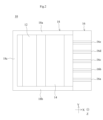
- FIG. 2 is a top view of the optical member 10.
- FIG. 3 is a perspective view of the optical device 1.
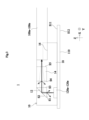
- FIG. 4 is an exploded view of the optical device 1.
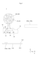
- FIG. 5 is a diagram of the lens portion 14 viewed in the negative direction of the X-axis.
- FIG. 6 is a perspective view of the optical device 1001.
- FIG. 7 is a perspective view of the optical device 1a.
- FIG. 8 is a perspective view of the optical device 1b.
- FIG. 9 is a perspective view of the gradient index lens 140.
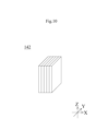
- FIG. 10 is a perspective view of the gradient index lens 142.
- FIG. 11 is a perspective view of the gradient index lenses 14a to 14e of the optical member 10c.
- FIG. 1 is a perspective view of the optical member 10.
- FIG. 2 is a top view of the optical member 10.
- FIG. 3 is a perspective view of the optical device 1.
- FIG. 4 is an exploded view of the optical device 1.
- FIG. 5 is a diagram of the lens portion 14 viewed in the negative direction of the X-axis.
- direction is defined as follows. As shown in FIG. 3, the direction in which the light emitting elements 120a to 120e emit light is defined as the positive direction of the Z axis. The direction in which the light reflected by the prism 12 travels is defined as the positive direction of the X-axis. The direction in which the optical fibers 100a to 100e are lined up is defined as the positive direction of the Y axis. The X-axis, Y-axis, and Z-axis are orthogonal to each other. Moreover, the X-axis, Y-axis, and Z-axis in this embodiment do not need to correspond with the X-axis, Y-axis, and Z-axis when the optical device 1 is used.
- the optical device 1 is a transmitting device of an optical communication system. As shown in FIGS. 3 and 4, the optical device 1 includes an optical member 10, optical fibers 100a to 100e, a circuit board 110, and light emitting elements 120a to 120e.
- the optical member 10 has a function of forming an optical path, a function of condensing light, and a function of changing the traveling direction of light. More specifically, the optical member 10 includes a prism 12, a lens section 14, a holding section 16, and a frame 18, as shown in FIGS. 1 and 2.
- the prism 12 is a second optical element that includes a medium M2 and a plurality of fillers P2 provided in the medium M2 and having an aspherical shape.
- the prism 12 changes the traveling direction of light passing through the medium M2.
- the prism 12 has a right isosceles triangular shape when viewed in the Y-axis direction.
- the prism 12 has an entrance surface S1 through which light enters, a reflection surface S2 through which light is reflected, and an exit surface S3 through which light exits.
- the entrance surface S1 has a normal line extending toward the negative direction of the Z axis.
- the reflective surface S2 has a normal line extending in the positive direction of the Z-axis and in the negative direction of the X-axis.
- the exit surface S3 has a normal extending in the positive direction of the X-axis.
- the medium M2 of the prism 12 is glass.
- Glass is a material that is amorphous and exhibits a glass transition phenomenon.
- the glass include simple oxide glasses such as SiO 2 , B 2 O 3 , P 2 O 5 , GeO 2 , As 2 O 3 , Li 2 O--SiO 2 , Na 2 O--SiO 2 , K 2 silicate glasses such as O-SiO 2 , aluminosilicate glasses such as Na 2 O-Al 2 O 3 -SiO 2 , CaO-Al 2 O 3 -SiO 2 , LiO 2 -Ba 2 -O 3 , Borate glasses such as Na2O - B2O3 , aluminoborate glasses such as CaO- Al2O3 - B2O3 , Na2O - Al2O3 -B2O3 - SiO It is a second class borosilicate glass.
- the plurality of fillers P2 are metal oxide particles such as crystalline silica, amorphous silica, alumina, magnesium oxide, and titanium oxide.
- the refractive index of the plurality of fillers is a value between the upper limit value n1 and the lower limit value n2 of the refractive index of the medium M2 of the prism 12 (second optical element).
- the refractive index of the plurality of fillers P2 and the refractive index of the medium M2 be close to each other.
- the higher the amorphousness of the plurality of fillers P2 the higher the transparency of the plurality of fillers P2.
- the plurality of fillers P2 have a non-spherical shape.
- a non-spherical shape is a shape that is not a sphere.
- a non-spherical shape is a shape in which the distance from the center to the outer edge is not constant, such as a rectangular parallelepiped shape or an ellipsoidal shape.
- the non-spherical shape may be a shape in which a large number of irregularities are provided on the surface of a sphere.
- the plurality of fillers P2 have an ellipsoidal shape.
- the plurality of fillers P2 have a longitudinal direction and a lateral direction. The longitudinal direction is the length direction of the longest portion of the plurality of fillers P2.
- the lateral direction is the length direction of the shortest portion of the plurality of fillers P2 among the directions orthogonal to the longitudinal direction.
- L1 be the length of the plurality of fillers P2 in the longitudinal direction.
- L2 be the length of the plurality of fillers P2 in the lateral direction.
- the wavelength of light be ⁇ .
- L2/L1>L1/ ⁇ holds true. Note that L1 and L2 are average values of 20 of the plurality of fillers P2 included in the prism 12.
- the plurality of fillers P2 are uniformly dispersed throughout the prism 12. Thereby, the plurality of fillers P2 are provided on the optical path. In particular, the plurality of fillers P2 are provided on the entrance surface S1.
- the lens section 14 includes gradient index lenses 14a to 14e and a support section 14f.
- the gradient index lenses 14a to 14e are arranged in this order toward the positive direction of the Y-axis. Since the gradient index lenses 14a to 14e have the same structure, the gradient index lens 14a will be described as an example.
- the gradient index lens 14a has a cylindrical shape with a central axis extending in the front-rear direction.
- the gradient index lens 14a has an entrance surface S4 and an exit surface S5, as shown in FIG.
- the entrance surface S4 and the exit surface S5 are arranged in this order in the positive direction of the X-axis.
- the entrance surface S4 has a normal line extending toward the negative direction of the X-axis.
- the exit surface S5 has a normal extending in the positive direction of the X-axis.
- the gradient index lens 14a is a first optical element that includes a medium M1 and a plurality of fillers P1 provided in the medium M1 and having an aspherical shape.
- the gradient index lens 14a changes the traveling direction of light passing through the medium M1. Specifically, as shown in FIG. 5, the refractive index of the gradient index lens 14a decreases as it moves away from the central axis of the gradient index lens 14a when viewed in the X-axis direction. Thereby, as shown in FIG. 3, the gradient index lens 14a condenses the light traveling in the positive direction of the X-axis within the medium M1 to a focal point located on the central axis of the gradient index lens 14a. . The focal point is located on the positive side of the X-axis from the exit surface S5. As a result, the gradient index lens 14a can change the diameter of light.
- the medium M1 of the gradient index lens 14a is glass.
- Glass is a material that is amorphous and exhibits a glass transition phenomenon.
- the glass include simple oxide glasses such as SiO 2 , B 2 O 3 , P 2 O 5 , GeO 2 , As 2 O 3 , Li 2 O-SiO 2 , Na 2 O-SiO 2 , K 2 silicate glasses such as O-SiO 2 , aluminosilicate glasses such as Na 2 O-Al 2 O 3 -SiO 2 , CaO-Al 2 O 3 -SiO 2 , LiO 2 -Ba 2 -O 3 , Borate glasses such as Na2O - B2O3 , aluminoborate glasses such as CaO- Al2O3 - B2O3 , Na2O - Al2O3 -B2O3 - SiO It is a second class borosilicate glass.
- Examples of methods for giving the gradient index lens 14a a refractive index distribution include the method described below. By impregnating cylindrical glass with molten salt, ions in the glass are replaced with ions in the molten salt, and metal ions permeate the cylindrical glass.
- the plurality of fillers P1 are metal oxide particles such as crystalline silica, amorphous silica, alumina, magnesium oxide, and titanium oxide.
- the refractive index of the plurality of fillers P1 is a value between the upper limit value n1 and the lower limit value n2 of the refractive index of the medium M1 of the gradient index lens 14a (first optical element).
- the refractive index of the plurality of fillers P1 and the refractive index of the medium M1 be close to each other.
- the plurality of fillers P1 have a non-spherical shape. Specifically, the plurality of fillers P1 have an ellipsoidal shape.
- the plurality of fillers P1 have a longitudinal direction and a lateral direction.
- the longitudinal direction is the length direction of the longest portion of the plurality of fillers P1.
- the lateral direction is the length direction of the shortest portion of the plurality of fillers P1 among the directions perpendicular to the longitudinal direction.
- L1 be the length of the plurality of fillers P1 in the longitudinal direction.
- L2 be the length of the plurality of fillers P1 in the lateral direction.
- the wavelength of light be ⁇ . At this time, L2/L1>L1/ ⁇ holds true. Note that L1 and L2 are average values of 20 fillers among the plurality of fillers P1 included in the gradient index lens 14a.
- the plurality of fillers P1 are uniformly dispersed throughout the gradient index lenses 14a to 14e. Thereby, the plurality of fillers P1 are provided on the optical path. In particular, the plurality of fillers P1 are provided on the entrance surface S4.
- the support portion 14f supports the gradient index lenses 14a to 14e. Specifically, the support portion 14f has an ellipsoidal shape.
- the gradient index lenses 14a to 14e are embedded in the support portion 14f. However, each of the entrance surfaces S4 of the gradient index lenses 14a to 14e is exposed from the negative side surface of the X-axis of the support portion 14f. Each of the exit surfaces S5 of the gradient index lenses 14a to 14e is exposed from the surface of the support portion 14f on the positive side of the X-axis.
- the material of the support portion 14f is the same glass as the medium M1 of the gradient index lens 14a.
- the gradient index lenses 14a to 14e as described above are located on the positive side of the X-axis of the prism 12. Thereby, the entrance surface S4 of the gradient index lenses 14a to 14e overlaps the exit surface S3 of the prism 12 when viewed in the X-axis direction.
- the holding part 16 holds the optical fiber 100a so that each of the lights emitted from the gradient index lenses 14a to 14e (first optical element) is incident on the end surface T of the optical fibers 100a to 100e. ⁇ Hold 100e. More specifically, the holding part 16 is located on the positive side of the X-axis of the lens part 14. As shown in FIG. 1, the holding portion 16 has a plate shape having a positive principal surface SP and a negative principal surface SM. The positive principal surface SP and the negative principal surface SM are arranged in this order in the negative direction of the Z-axis. Further, grooves 16a to 16e extending in the X-axis direction are provided on the front main surface SP of the holding portion 16.
- the grooves 16a to 16e are arranged in this order in the positive direction of the Y-axis.
- Each of the optical fibers 100a to 100e is fixed to the grooves 16a to 16e with an adhesive.
- the optical axes of the optical fibers 100a to 100e coincide with the central axes of the gradient index lenses 14a to 14e.
- the material of the holding part 16 is the same glass as the medium M2 of the prism 12 and the medium M1 of the gradient index lens 14a.
- the frame 18 supports the prism 12, the lens section 14, and the holding section 16. More specifically, the frame 18 includes support parts 18a, 18b and a connecting part 18c. Each of the support parts 18a and 18b is a plate having two main surfaces aligned in the Y-axis direction. The support portions 18a and 18b are arranged in this order in the negative direction of the Y-axis. The end of the holding portion 16 on the positive side of the Y-axis and the end of the lens portion 14 on the positive side of the Y-axis are in contact with the support portion 18a. The Y-axis negative end of the holding portion 16 and the Y-axis negative end of the lens portion 14 are in contact with the support portion 18b. The surface of the holding portion 16 located on the negative side of the X-axis is in contact with the positive end of the support portion 18a in the X-axis direction and the positive end of the support portion 18b in the X-axis direction.
- the connecting portion 18c is a plate having two main surfaces aligned in the X-axis direction.
- the end of the connecting portion 18c on the positive side of the Y axis is in contact with the supporting portion 18a.
- the Y-axis negative end of the connecting portion 18c is in contact with the supporting portion 18b.
- the material of the holding part 16 is the same glass as the medium M2 of the prism 12 and the medium M1 of the gradient index lens 14a.
- the lens portion 14 (first optical element), prism 12 (second optical element), holding portion 16, and frame 18 as described above are integrally molded. That is, the lens portion 14 (first optical element), prism 12 (second optical element), holding portion 16, and frame 18 cannot be separated without damaging them.
- the circuit board 110 has a plate shape, as shown in FIGS. 3 and 4. Therefore, the circuit board 110 has a positive principal surface S11 and a negative principal surface S12.
- the positive principal surface S11 is located on the positive side of the Z axis of the negative principal surface S12. Electric circuits such as wiring are provided on the surface and inside of the circuit board 110.
- the circuit board 110 is located on the negative side of the optical member 10 in the Z-axis direction.
- the light emitting elements 120a to 120e emit light in the positive direction of the Z axis.
- the light emitting elements 120a to 120e are, for example, vertical cavity surface emitting lasers (VCSEL).
- the wavelength of the light is, for example, 1310 nm.
- the light emitting elements 120a to 120e are mounted on the front main surface S11 of the circuit board 110.
- the light emitting elements 120a to 120e overlap the entrance surface S1 of the prism 12 when viewed in the Z-axis direction.
- the light emitting elements 120a to 120e emit light in the positive direction of the Z axis.
- the light travels in the positive direction of the Z-axis while the diameter expands in a direction perpendicular to the direction of travel, or while the diameter remains unchanged.
- the light emitted by the light emitting elements 120a to 120e enters the prism 12 (second optical element) via the entrance surface S1.
- the light travels in the positive direction of the X-axis by being reflected by the reflective surface S2.
- the light then exits from the prism 12 via the exit surface S3.
- the light emitted from the prism 12 enters the gradient index lenses 14a to 14e (first optical element) via the entrance surface S4.
- the light is focused when passing through the gradient index lenses 14a to 14e.
- the light then exits from the gradient index lenses 14a to 14e via the exit surface S5. After this, the light enters the optical fibers 100a-100e.
- FIG. 6 is a perspective view of the optical device 1001.
- the optical device 1001 differs from the optical device 1 in that the prism 1012 does not include a plurality of fillers P2, and the gradient index lenses 1014a to 1014e (not shown) do not include a plurality of fillers P1. .
- the semiconductor optical coupling device described in Patent Document 1 includes an optical isolator.
- the gradient index lenses 14a to 14e include a plurality of fillers P1.
- the prism 12 includes a plurality of fillers P2.
- part of the light is reflected by the plurality of fillers P1 while traveling in the medium M1.
- part of the light is reflected by the plurality of fillers P2 while traveling in the medium M2.
- the plurality of fillers P1 and P2 have a non-spherical shape. Therefore, the light reflected by the plurality of fillers P1 does not travel in the negative direction of the X-axis, as shown in FIG. 3.
- the light reflected by the plurality of fillers P2 does not travel in the negative direction of the Z-axis. Therefore, the light reflected by the plurality of fillers P1 and P2 becomes difficult to enter the light emitting elements 120a to 120e.
- the optical member 10 by providing the plurality of fillers P1 and P2 without adding a new element, reflected light is suppressed from entering the light emitting elements 120a to 120e. Therefore, the size of the optical member 10 and the cost of the optical member 10 can be reduced.
- the plurality of fillers P1 and P2 are provided on the optical path. Thereby, light becomes more likely to be reflected by the plurality of fillers P1 and P2.
- the plurality of fillers P1 and P2 are provided on the entrance surfaces S1 and S4.
- the light reflected by the incident surface S1 is reflected by the plurality of fillers P2 in a direction other than the negative direction of the Z axis.
- the light reflected by the entrance surface S4 is reflected by the plurality of fillers P1 in a direction other than the negative direction of the X-axis.
- the light reflected by the plurality of fillers P1 and P2 becomes difficult to enter the light emitting elements 120a to 120e.
- the refractive index of the plurality of fillers P1 is a value between the upper limit value n1 and the lower limit value n2 of the refractive index of the medium M1 of the gradient index lenses 14a to 14e. Therefore, the influence of the plurality of fillers P1 on the optical characteristics of the gradient index lenses 14a to 14e can be reduced.
- the length of the plurality of fillers P1 and P2 in the longitudinal direction is L1
- the length of the plurality of fillers P1 and P2 in the transverse direction is L2
- the wavelength of light is ⁇
- L2/L1>L1/ ⁇ holds true.
- Rayleigh scattering occurs.
- Spherical fillers increase backscattered components due to Rayleigh scattering, but non-spherical fillers can suppress this.
- the prism 12 and the gradient index lenses 14a to 14e are integrally molded. This suppresses variations in the positional relationship between the prism 12 and the gradient index lenses 14a to 14e.
- FIG. 7 is a perspective view of the optical device 1a.
- the optical member 10a differs from the optical member 10 in that it does not include a prism 12.
- each of the light emitting elements 120a to 120e is located on the negative side of the X axis of the gradient index lenses 14a to 14e. Then, the light emitted from each of the light emitting elements 120a to 120e enters the gradient index lenses 14a to 14e (first optical elements).
- the other structure of the optical member 10a is the same as that of the optical member 10, so a description thereof will be omitted.
- the optical member 10a can have the same effects as the optical member 10.
- FIG. 8 is a perspective view of the optical device 1b.
- FIG. 9 is a perspective view of the gradient index lens 140.
- FIG. 10 is a perspective view of the gradient index lens 142.
- the optical member 10b differs from the optical member 10a in that it includes a gradient index lens 140 (first optical element) and a gradient index lens 142 instead of gradient index lenses 14a to 14e (first optical elements). It differs from The refractive index of the gradient index lens 140 decreases as it moves away from the center in the Z-axis direction in the positive and negative directions of the Z-axis direction. Thereby, the gradient index lens 140 condenses light traveling in the positive direction of the X-axis so that the diameter thereof becomes smaller in the Z-axis direction. Further, the gradient index lens 140 includes a medium and a plurality of fillers.
- the refractive index of the gradient index lens 142 decreases as it moves away from the center in the Y-axis direction in the positive and negative directions of the Y-axis direction.
- the gradient index lens 142 condenses light traveling in the positive direction of the X-axis so that the diameter thereof becomes smaller in the Y-axis direction.
- the gradient index lens 142 includes a medium and a plurality of fillers.
- optical member 10b The other structure of the optical member 10b is the same as that of the optical member 10a, so a description thereof will be omitted.
- the optical member 10b can have the same effects as the optical member 10a.
- FIG. 11 is a perspective view of the gradient index lenses 14a to 14e of the optical member 10c.
- the optical member 10c differs from the optical member 10 in the positions where the plurality of fillers P1 are provided. More specifically, the gradient index lenses 14a to 14e have a focal point. The condensing point is a position where the diameter of light is the smallest in the gradient index lenses 14a to 14e (first optical element). The plurality of fillers P1 are located at the focal point. Thereby, the light is effectively scattered by the plurality of fillers P1.
- the rest of the structure of the optical member 10c is the same as that of the optical member 10, so a description thereof will be omitted.
- the optical member 10c can have the same effects as the optical member 10.
- optical member according to the present invention is not limited to the optical members 10, 10a to 10c, and can be modified within the scope of the gist thereof. Furthermore, the structures of the optical members 10, 10a to 10c may be combined arbitrarily.
- first optical element and the second optical element may be optical elements other than the prism and the gradient index lens.
- the plurality of fillers may be provided at positions other than the light condensing point. Further, the plurality of fillers may not be provided at the light condensing point.
- the plurality of fillers do not need to be provided on the incident surface.
- the optical device may include a receiving device in addition to the transmitting device. That is, the optical device may include a light receiving element in addition to the light emitting element.
- the first optical element and the second optical element corresponding to the light emitting element may include a medium and a plurality of fillers.
- the positions of the gradient index lens 140 and the gradient index lens 142 may be switched.
- the optical member may not include a gradient index lens but may include a prism.
- the prism is the first optical element.
- the refractive index of the gradient index lens may change stepwise.
- Optical device 10 10a to 10c: Optical member 12: Prism 14: Lens parts 14a to 14e, 140, 142: Gradient index lens 14f: Supporting part 16: Holding parts 16a to 16e: Groove 18 : Frame bodies 18a, 18b: Support part 18c: Connecting parts 100a to 100e: Optical fiber 110: Circuit board 120a to 120e: Light emitting elements M1, M2: Medium P1, P2: Filler S1, S4: Incident surface S11, SP: Positive Principal surface S12, SM: Negative principal surface S2: Reflective surface S3, S5: Output surface T: End surface
Landscapes
- Physics & Mathematics (AREA)
- General Physics & Mathematics (AREA)
- Optics & Photonics (AREA)
- Optical Couplings Of Light Guides (AREA)
- Optical Elements Other Than Lenses (AREA)
Priority Applications (3)
| Application Number | Priority Date | Filing Date | Title |
|---|---|---|---|
| CN202280089418.7A CN118575110A (zh) | 2022-03-17 | 2022-10-28 | 光学构件以及光学装置 |
| JP2024507499A JP7568164B2 (ja) | 2022-03-17 | 2022-10-28 | 光学部材及び光学装置 |
| US18/775,101 US20240369782A1 (en) | 2022-03-17 | 2024-07-17 | Optical member and optical device |
Applications Claiming Priority (2)
| Application Number | Priority Date | Filing Date | Title |
|---|---|---|---|
| JP2022-042718 | 2022-03-17 | ||
| JP2022042718 | 2022-03-17 |
Related Child Applications (1)
| Application Number | Title | Priority Date | Filing Date |
|---|---|---|---|
| US18/775,101 Continuation US20240369782A1 (en) | 2022-03-17 | 2024-07-17 | Optical member and optical device |
Publications (1)
| Publication Number | Publication Date |
|---|---|
| WO2023176037A1 true WO2023176037A1 (ja) | 2023-09-21 |
Family
ID=88023218
Family Applications (1)
| Application Number | Title | Priority Date | Filing Date |
|---|---|---|---|
| PCT/JP2022/040455 Ceased WO2023176037A1 (ja) | 2022-03-17 | 2022-10-28 | 光学部材及び光学装置 |
Country Status (4)
| Country | Link |
|---|---|
| US (1) | US20240369782A1 (https=) |
| JP (1) | JP7568164B2 (https=) |
| CN (1) | CN118575110A (https=) |
| WO (1) | WO2023176037A1 (https=) |
Cited By (3)
| Publication number | Priority date | Publication date | Assignee | Title |
|---|---|---|---|---|
| WO2025022695A1 (ja) * | 2023-07-26 | 2025-01-30 | 株式会社村田製作所 | 光結合器、光電変換回路モジュール及び光トランシーバ |
| WO2025022694A1 (ja) * | 2023-07-26 | 2025-01-30 | 株式会社村田製作所 | 光結合器の製造方法、光結合器、光電変換回路モジュール及び光トランシーバ |
| WO2026058583A1 (ja) * | 2024-09-12 | 2026-03-19 | パナソニックIpマネジメント株式会社 | 光学システムおよび光コネクタ |
Citations (7)
| Publication number | Priority date | Publication date | Assignee | Title |
|---|---|---|---|---|
| JPS556320A (en) * | 1978-06-27 | 1980-01-17 | Ritsuo Hasumi | Spectral module |
| US5026160A (en) * | 1989-10-04 | 1991-06-25 | The United States Of America As Represented By The Secretary Of The Navy | Monolithic optical programmable spectrograph (MOPS) |
| JP2005321651A (ja) * | 2004-05-10 | 2005-11-17 | Seiko Epson Corp | 光通信モジュール |
| JP2007304298A (ja) * | 2006-05-11 | 2007-11-22 | Central Glass Co Ltd | 光能動素子実装基板 |
| JP2009037001A (ja) * | 2007-08-01 | 2009-02-19 | National Institute Of Advanced Industrial & Technology | 光結合用接着剤とそれを用いた光結合方法 |
| WO2009054229A1 (ja) * | 2007-10-25 | 2009-04-30 | Konica Minolta Opto, Inc. | 光学素子の製造方法 |
| WO2020150551A1 (en) * | 2019-01-18 | 2020-07-23 | Samtec, Inc. | Sealed optical transceiver |
-
2022
- 2022-10-28 JP JP2024507499A patent/JP7568164B2/ja active Active
- 2022-10-28 CN CN202280089418.7A patent/CN118575110A/zh active Pending
- 2022-10-28 WO PCT/JP2022/040455 patent/WO2023176037A1/ja not_active Ceased
-
2024
- 2024-07-17 US US18/775,101 patent/US20240369782A1/en active Pending
Patent Citations (7)
| Publication number | Priority date | Publication date | Assignee | Title |
|---|---|---|---|---|
| JPS556320A (en) * | 1978-06-27 | 1980-01-17 | Ritsuo Hasumi | Spectral module |
| US5026160A (en) * | 1989-10-04 | 1991-06-25 | The United States Of America As Represented By The Secretary Of The Navy | Monolithic optical programmable spectrograph (MOPS) |
| JP2005321651A (ja) * | 2004-05-10 | 2005-11-17 | Seiko Epson Corp | 光通信モジュール |
| JP2007304298A (ja) * | 2006-05-11 | 2007-11-22 | Central Glass Co Ltd | 光能動素子実装基板 |
| JP2009037001A (ja) * | 2007-08-01 | 2009-02-19 | National Institute Of Advanced Industrial & Technology | 光結合用接着剤とそれを用いた光結合方法 |
| WO2009054229A1 (ja) * | 2007-10-25 | 2009-04-30 | Konica Minolta Opto, Inc. | 光学素子の製造方法 |
| WO2020150551A1 (en) * | 2019-01-18 | 2020-07-23 | Samtec, Inc. | Sealed optical transceiver |
Cited By (3)
| Publication number | Priority date | Publication date | Assignee | Title |
|---|---|---|---|---|
| WO2025022695A1 (ja) * | 2023-07-26 | 2025-01-30 | 株式会社村田製作所 | 光結合器、光電変換回路モジュール及び光トランシーバ |
| WO2025022694A1 (ja) * | 2023-07-26 | 2025-01-30 | 株式会社村田製作所 | 光結合器の製造方法、光結合器、光電変換回路モジュール及び光トランシーバ |
| WO2026058583A1 (ja) * | 2024-09-12 | 2026-03-19 | パナソニックIpマネジメント株式会社 | 光学システムおよび光コネクタ |
Also Published As
| Publication number | Publication date |
|---|---|
| US20240369782A1 (en) | 2024-11-07 |
| CN118575110A (zh) | 2024-08-30 |
| JP7568164B2 (ja) | 2024-10-16 |
| JPWO2023176037A1 (https=) | 2023-09-21 |
Similar Documents
| Publication | Publication Date | Title |
|---|---|---|
| JP7568164B2 (ja) | 光学部材及び光学装置 | |
| JP6429921B2 (ja) | 光分岐モジュール | |
| US9995892B2 (en) | Optical communication modules | |
| JP6810596B2 (ja) | 波長分割多重デバイス、波長分割多重システム、および波長分割多重デバイスを形成する方法 | |
| US10386575B2 (en) | Optical assembly and method for coupling a waveguide array to a photonic-integrated circuit | |
| WO2013140922A1 (ja) | 光レセプタクルおよびこれを備えた光モジュール | |
| US9500819B2 (en) | Optical module | |
| US10649147B2 (en) | Optical module | |
| JP2012194372A (ja) | レンズアレイおよびこれを備えた光モジュール | |
| KR20240127265A (ko) | 파이버 대 칩 통합을 위한 광학 커플링 어댑터 | |
| WO2023181496A1 (ja) | 光接続ユニット | |
| JP2010008542A (ja) | 光伝送モジュール | |
| US20230236368A1 (en) | Optical module package using bi-angled silica waveguide | |
| JP2017134228A (ja) | 光導波路 | |
| JP2025018126A (ja) | 光結合器、光電変換回路モジュール及び光トランシーバ | |
| US20180306973A1 (en) | Housing for Packaging Optical Transmitter Module and Optical Transmitter Module | |
| US20230090783A1 (en) | Optical wiring component | |
| JP2016212414A (ja) | 導波路用結合回路 | |
| JP2025018125A (ja) | 光結合器、光電変換回路モジュール及び光トランシーバ | |
| WO2023026574A1 (ja) | 光学素子 | |
| JP7782721B2 (ja) | 光結合器、光電変換回路モジュール及び光トランシーバ | |
| JP7835298B2 (ja) | 光結合器の製造方法、光結合器、光電変換回路モジュール及び光トランシーバ | |
| JP6796627B2 (ja) | 光コネクタ部、及び、光接続構造体 | |
| US10302883B2 (en) | Optical coupling assemblies | |
| JPH11218638A (ja) | 光学構成素子 |
Legal Events
| Date | Code | Title | Description |
|---|---|---|---|
| 121 | Ep: the epo has been informed by wipo that ep was designated in this application |
Ref document number: 22932300 Country of ref document: EP Kind code of ref document: A1 |
|
| WWE | Wipo information: entry into national phase |
Ref document number: 2024507499 Country of ref document: JP |
|
| WWE | Wipo information: entry into national phase |
Ref document number: 202280089418.7 Country of ref document: CN |
|
| NENP | Non-entry into the national phase |
Ref country code: DE |
|
| 122 | Ep: pct application non-entry in european phase |
Ref document number: 22932300 Country of ref document: EP Kind code of ref document: A1 |