WO2023167161A1 - 半導体装置 - Google Patents
半導体装置 Download PDFInfo
- Publication number
- WO2023167161A1 WO2023167161A1 PCT/JP2023/007193 JP2023007193W WO2023167161A1 WO 2023167161 A1 WO2023167161 A1 WO 2023167161A1 JP 2023007193 W JP2023007193 W JP 2023007193W WO 2023167161 A1 WO2023167161 A1 WO 2023167161A1
- Authority
- WO
- WIPO (PCT)
- Prior art keywords
- region
- ring
- concentration
- well
- regions
- Prior art date
- Legal status (The legal status is an assumption and is not a legal conclusion. Google has not performed a legal analysis and makes no representation as to the accuracy of the status listed.)
- Ceased
Links
Images







Classifications
-
- H—ELECTRICITY
- H10—SEMICONDUCTOR DEVICES; ELECTRIC SOLID-STATE DEVICES NOT OTHERWISE PROVIDED FOR
- H10D—INORGANIC ELECTRIC SEMICONDUCTOR DEVICES
- H10D89/00—Aspects of integrated devices not covered by groups H10D84/00 - H10D88/00
- H10D89/60—Integrated devices comprising arrangements for electrical or thermal protection, e.g. protection circuits against electrostatic discharge [ESD]
- H10D89/601—Integrated devices comprising arrangements for electrical or thermal protection, e.g. protection circuits against electrostatic discharge [ESD] for devices having insulated gate electrodes, e.g. for IGFETs or IGBTs
- H10D89/611—Integrated devices comprising arrangements for electrical or thermal protection, e.g. protection circuits against electrostatic discharge [ESD] for devices having insulated gate electrodes, e.g. for IGFETs or IGBTs using diodes as protective elements
-
- H—ELECTRICITY
- H10—SEMICONDUCTOR DEVICES; ELECTRIC SOLID-STATE DEVICES NOT OTHERWISE PROVIDED FOR
- H10D—INORGANIC ELECTRIC SEMICONDUCTOR DEVICES
- H10D30/00—Field-effect transistors [FET]
- H10D30/01—Manufacture or treatment
- H10D30/021—Manufacture or treatment of FETs having insulated gates [IGFET]
-
- H—ELECTRICITY
- H10—SEMICONDUCTOR DEVICES; ELECTRIC SOLID-STATE DEVICES NOT OTHERWISE PROVIDED FOR
- H10D—INORGANIC ELECTRIC SEMICONDUCTOR DEVICES
- H10D30/00—Field-effect transistors [FET]
- H10D30/60—Insulated-gate field-effect transistors [IGFET]
-
- H—ELECTRICITY
- H10—SEMICONDUCTOR DEVICES; ELECTRIC SOLID-STATE DEVICES NOT OTHERWISE PROVIDED FOR
- H10D—INORGANIC ELECTRIC SEMICONDUCTOR DEVICES
- H10D84/00—Integrated devices formed in or on semiconductor substrates that comprise only semiconducting layers, e.g. on Si wafers or on GaAs-on-Si wafers
-
- H—ELECTRICITY
- H10—SEMICONDUCTOR DEVICES; ELECTRIC SOLID-STATE DEVICES NOT OTHERWISE PROVIDED FOR
- H10D—INORGANIC ELECTRIC SEMICONDUCTOR DEVICES
- H10D84/00—Integrated devices formed in or on semiconductor substrates that comprise only semiconducting layers, e.g. on Si wafers or on GaAs-on-Si wafers
- H10D84/01—Manufacture or treatment
- H10D84/02—Manufacture or treatment characterised by using material-based technologies
- H10D84/03—Manufacture or treatment characterised by using material-based technologies using Group IV technology, e.g. silicon technology or silicon-carbide [SiC] technology
- H10D84/038—Manufacture or treatment characterised by using material-based technologies using Group IV technology, e.g. silicon technology or silicon-carbide [SiC] technology using silicon technology, e.g. SiGe
Definitions
- the present disclosure relates to semiconductor devices.
- MOSFET metal-oxide-semiconductor field-effect transistor
- a semiconductor device is a semiconductor device including a MOSFET, comprising: a semiconductor layer of a first conductivity type; a body region of a second conductivity type formed on a surface of the semiconductor layer; a drain region of a second conductivity type formed in a surface, spaced apart from the semiconductor layer around the body region, and extending in a first direction orthogonal to a thickness direction of the semiconductor layer; and a surface of the semiconductor layer.
- a first well region of a first conductivity type formed separately from the drain region in a second direction perpendicular to both the thickness direction of the semiconductor layer and the first direction; a gate insulating film formed on the semiconductor layer between the region and the body region; and a field oxide film formed on a surface of the body region between the gate insulating film and the drain region.
- a gate electrode formed on the gate insulating film and the field oxide film, a second conductivity type source region formed on the surface of the first well region, and a thickness direction of the semiconductor layer, , an exposed region formed in the first well region at a position different from the source region, a first contact portion joined to the source region, and a second contact portion joined to the exposed region in a Schottky junction; , a third contact portion joined to the gate electrode; and wiring electrically connecting the first contact portion, the second contact portion, and the third contact portion to each other.
- a semiconductor device is a semiconductor device including a MOSFET, and includes: a semiconductor layer of a second conductivity type; a drain region of a first conductivity type extending in the direction of the semiconductor layer; a first conductivity type source region, a gate insulating film formed on the semiconductor layer between the drain region and the source region, a gate electrode formed on the gate insulating film; a ring-shaped region which is a semiconductor region of the second conductivity type formed in a ring shape so as to surround both the drain region and the source region; an exposed region formed in a position different from the high-concentration region in the ring-shaped region when viewed from the thickness direction of the semiconductor layer; and a first ring joined to the high-concentration region a second ring-side contact portion Schottky-junctioned to the exposed region; and a wiring electrically connecting the first ring-side contact portion, the second ring-side contact portion, and the gate electrode to each other. And prepare.
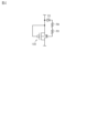
- FIG. 1 is a circuit diagram showing an example of a circuit configuration of a semiconductor integrated circuit including a protection circuit according to the first embodiment.
- FIG. 2 is a plan view schematically showing an example of the planar structure of the second MOSFET of the protection circuit.
- FIG. 3 is a cross-sectional view schematically showing the cross-sectional structure of the second MOSFET taken along line F3-F3 of FIG.
- FIG. 4 is a circuit diagram showing the second MOSFET and parasitic elements.
- FIG. 5 is a plan view schematically showing a planar structure of a comparative MOSFET.
- FIG. 6 is a cross-sectional view schematically showing the cross-sectional structure of the comparative MOSFET taken along line F6-F6 of FIG.
- FIG. 1 is a circuit diagram showing an example of a circuit configuration of a semiconductor integrated circuit including a protection circuit according to the first embodiment.
- FIG. 2 is a plan view schematically showing an example of the planar structure of the second MOSFET of the
- FIG. 7 is a circuit diagram showing comparative MOSFETs and parasitic elements.
- FIG. 8 is a characteristic diagram showing IV characteristics of the second MOSFET and the comparison MOSFET.
- FIG. 9 is a plan view schematically showing an example of the planar structure of the second MOSFET of the first modified example.
- FIG. 10 is a plan view schematically showing an example of the planar structure of the second MOSFET of the second modified example.
- FIG. 11 is a plan view schematically showing an example of the planar structure of the second MOSFET of the third modification.
- FIG. 12 is a plan view schematically showing an example of the planar structure of the second MOSFET of the fourth modification.
- FIG. 13 is a plan view schematically showing an example of the planar structure of the second MOSFET of the fifth modification.
- FIG. 14 is a plan view schematically showing an example of the planar structure of the second MOSFET of the sixth modification.
- FIG. 15 is a plan view schematically showing an example of the planar structure of the second MOSFET of the seventh modification.
- FIG. 16 is a plan view schematically showing an example of the planar structure of the second MOSFET of the eighth modification.
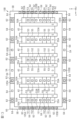
- FIG. 17 is a plan view schematically showing an example of the planar structure of the protection circuit of the second embodiment.
- 18 is a cross-sectional view schematically showing the cross-sectional structure of the protection circuit of FIG. 17.
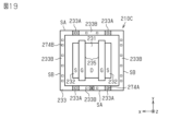
- FIG. 19 is a plan view schematically showing an example of the planar structure of the third MOSFET of the first modified example.
- FIG. 20 is a plan view schematically showing an example of the planar structure of the third MOSFET of the second modification.
- FIG. 1 A configuration in which the semiconductor device of the first embodiment is implemented as a protection circuit 10 will be described with reference to FIGS. 1 to 4.
- FIG. 1 A configuration in which the semiconductor device of the first embodiment is implemented as a protection circuit 10 will be described with reference to FIGS. 1 to 4.
- FIG. 1 A configuration in which the semiconductor device of the first embodiment is implemented as a protection circuit 10 will be described with reference to FIGS. 1 to 4.
- FIG. 1 A configuration in which the semiconductor device of the first embodiment is implemented as a protection circuit 10 will be described with reference to FIGS. 1 to 4.
- the protection circuit 10 is a circuit that is connected to a semiconductor integrated circuit (LSI) 1 including an internal circuit CIT formed with, for example, a plurality of transistors, and protects the internal circuit CIT from ESD.
- the semiconductor integrated circuit 1 has a package structure in which an internal circuit CIT is sealed with a sealing resin (not shown). In other words, the protection circuit 10 is sealed with the sealing resin together with the internal circuit CIT.
- the semiconductor integrated circuit 1 includes a power electrode PE, a ground electrode PG, and an input electrode PI connected to the internal circuit CIT. These electrodes PE, PG and PI are exposed from the sealing resin.
- the power supply electrode PE is an electrode that supplies power supply voltage to the internal circuit CIT.
- the ground electrode PG is an electrode used to connect the internal circuit CIT to the ground.
- the input electrode PI is an electrode that is electrically connected to an external control circuit and inputs a signal to the internal circuit CIT.
- the semiconductor integrated circuit 1 includes a first wiring W1 connected to the power electrode PE, a second wiring W2 connected to the ground electrode PG, and a third wiring W3 connected to the input electrode PI. Each wiring W1 to W3 is connected to the internal circuit CIT.
- the semiconductor integrated circuit 1 also includes a fourth wiring W4 that transmits a signal output from the internal circuit CIT.
- the protection circuit 10 is a circuit that protects the internal circuit CIT from current caused by ESD that tries to flow into the internal circuit CIT via the power supply electrode PE and the input electrode PI.
- the protection circuit 10 includes a first MOSFET 10A connected between the input electrode PI and the ground electrode PG, a second MOSFET 10B connected between the power electrode PE and the input electrode PI, and a MOSFET 10B connected between the power electrode PE and the ground electrode PG. and a third MOSFET 10C connected therebetween.
- the first MOSFET 10A can be said to be provided between the third wiring W3 and the second wiring W2, and the second MOSFET 10B can be said to be provided between the first wiring W1 and the third wiring W3. is provided between the first wiring W1 and the second wiring W2.
- Both the first MOSFET 10A and the third MOSFET 10C are n-type MOSFETs, and the second MOSFET 10B is a p-type MOSFET.
- the first MOSFET 10A and the second MOSFET 10B are connected in series. More specifically, the source of the second MOSFET 10B is connected to the power supply electrode PE (first wiring W1), and the drain of the second MOSFET 10B is connected to the input electrode PI (third wiring W3). The drain of the first MOSFET 10A is connected to the input electrode PI (third wiring W3), and the source of the first MOSFET 10A is connected to the ground electrode PG (second wiring W2). In the first embodiment, the source of the second MOSFET 10B is connected between the power electrode PE and the internal circuit CIT in the first wiring W1.
- the drain of the first MOSFET 10A and the drain of the second MOSFET 10B are connected between the input electrode PI of the third wiring W3 and the internal circuit CIT.
- the source of the first MOSFET 10A is connected between the ground electrode PG and the internal circuit CIT in the second wiring W2.
- the third MOSFET 10C is arranged on the opposite side of the internal circuit CIT from the first MOSFET 10A and the second MOSFET 10B.
- the drain of the third MOSFET 10C is connected to the first wiring W1, and the source of the third MOSFET 10C is connected to the second wiring W2.
- the gate of the first MOSFET 10A is connected to the source of the first MOSFET 10A through the first resistance element R1.
- the gate of the second MOSFET 10B is connected to the source of the second MOSFET 10B through the second resistance element R2.
- the gate of the third MOSFET 10C is connected to the source of the third MOSFET 10C via the third resistance element R3.
- the first to third resistance elements R1 to R3 are electrically connected between the gates and sources of the corresponding first to third MOSFETs 10A to 10C.
- the back gates of the first to third MOSFETs 10A to 10C are connected to the corresponding sources of the first to third MOSFETs 10A to 10C.
- FIG. 2 shows an example of a planar structure of the second MOSFET 10B that is part of the protection circuit 10.
- FIG. 3 shows an example of the cross-sectional structure of the second MOSFET 10B.
- FIG. 2 omits an element isolation region 70 and its surrounding structure, which will be described later.
- the source region 53 and the high-concentration region 54, which will be described later, and the source region 53 and the exposed region 55, which will be described later, are shown side by side.
- the protection circuit 10 includes a semiconductor substrate 20 and a first conductivity type (n-type in the first embodiment) semiconductor layer 30 formed on the semiconductor substrate 20 .
- Semiconductor substrate 20 is made of a material containing silicon (Si), for example.
- the semiconductor substrate 20 is a Si substrate.
- Semiconductor substrate 20 has a thickness of, for example, 100 ⁇ m or more and 700 ⁇ m or less.
- the impurity concentration of the semiconductor substrate 20 is 1 ⁇ 10 13 cm ⁇ 3 or more and 1 ⁇ 10 16 cm ⁇ 3 or less.
- the semiconductor layer 30 is, for example, a layer formed by epitaxial growth from the semiconductor substrate 20, and is made of, for example, a material containing Si.
- Semiconductor layer 30 has a thickness of, for example, 2 ⁇ m or more and 20 ⁇ m or less.
- the impurity concentration of the semiconductor layer 30 is 1 ⁇ 10 14 cm ⁇ 3 or more and 1 ⁇ 10 16 cm ⁇ 3 or less.
- the thickness direction of the semiconductor layer 30 is the "z direction”. Viewing the protection circuit 10 from the z-direction is referred to as "plan view”. In this case, planar view includes the meaning of "viewing from the thickness direction of the semiconductor layer 30".
- the two directions that are perpendicular to each other are referred to as the "x-direction" and the "y-direction", respectively.
- the y-direction corresponds to the "first direction”
- the x-direction corresponds to the "second direction”.
- the second MOSFET 10B is formed in the semiconductor layer 30 formed on the semiconductor substrate 20. As shown in FIG. Although not shown, both the first MOSFET 10A and the third MOSFET 10C are also formed in the semiconductor layer 30. As shown in FIG. The first MOSFET 10A and the third MOSFET 10C have the same configuration as the second MOSFET 10B except that the conductivity type is reversed. Therefore, in the following description, the configuration of the second MOSFET 10B will be described, and the description of the configurations of the first MOSFET 10A and the third MOSFET 10C will be omitted.
- the surface 30s of the semiconductor layer 30 includes a body region 40 of the second conductivity type (p-type in the first embodiment), a first well region 50A of the first conductivity type (n-type in the first embodiment), and a first well region 50A.
- a second well region 50B of the same first conductivity type as the first well region 50A is provided.
- a ring-shaped region 60 formed in a ring shape so as to surround the body region 40, the first well region 50A and the second well region 50B, and a second well region 60 surrounding the ring-shaped region 60
- a conductive type (p-type in the first embodiment) element isolation region 70 is provided on the surface 30s of the semiconductor layer 30.
- the ring-shaped region 60 is a semiconductor region of the first conductivity type (n-type in the first embodiment).
- the portion surrounded by the element isolation region 70 is the element formation region of the second MOSFET 10B.
- the element forming region is the region in which the body region 40, the first well region 50A and the second well region 50B are formed.
- a ring-shaped region 60 is formed in the element forming region.
- a plurality of body regions 40, a plurality of first well regions 50A, and a plurality of second well regions 50B may be formed in the element forming region. As shown in FIG. 2, in the first embodiment, two body regions 40, one first well region 50A, and two second well regions 50B are formed side by side in the element formation region.
- the direction in which the body regions 40, the first well regions 50A, and the second well regions 50B are arranged is defined as the x direction.
- the semiconductor layer 30 is interposed between the body region 40 and the first well region 50A and the second well region 50B in the x direction.
- the first well region 50A is arranged in the center of the element formation region in the second direction (x direction).
- the two second well regions 50B are distributed on both sides of the first well region 50A in the x direction.
- the body region 40 is arranged between the second well region 50B and the first well region 50A in the x direction.
- the two second well regions 50B are arranged at both ends of the element formation region in the second direction (x direction).
- the first well region 50A and the second well region 50B are arranged with the body region 40 interposed therebetween in the second direction (x direction).
- the number of body regions 40, first well regions 50A, and second well regions 50B in the element forming region can be changed arbitrarily.
- Body region 40 extends in the y direction. That is, the body region 40 extends in a first direction perpendicular to the arrangement direction (x direction, second direction) of the body region 40, the first well region 50A, and the second well region 50B in plan view.
- the width dimension (dimension in the x direction) of the body region 40 is larger than the width dimension (dimension in the x direction) of the first well region 50A.
- Body region 40 has a higher impurity concentration than semiconductor layer 30 .
- the impurity concentration of the body region 40 of the first embodiment is 1 ⁇ 10 15 cm ⁇ 3 or more and 1 ⁇ 10 17 cm ⁇ 3 or less.
- An intermediate body region 41 of the second conductivity type (p type in the first embodiment) is formed on the surface 40s of the body region 40 .
- the intermediate body region 41 is arranged apart from the semiconductor layer 30 surrounding the body region 40 .
- Intermediate body region 41 extends in the y-direction.
- Intermediate body region 41 has a higher impurity concentration than body region 40 .
- the impurity concentration of the intermediate body region 41 of the first embodiment is 1 ⁇ 10 17 cm ⁇ 3 or more and 1 ⁇ 10 19 cm ⁇ 3 or less.
- a drain region 42 of the second conductivity type (p + type in the first embodiment) is formed on the surface of the intermediate body region 41 . It can also be said that the drain region 42 is formed on the surface 40 s of the body region 40 . Like the intermediate body region 41 , the drain region 42 is arranged apart from the semiconductor layer 30 surrounding the body region 40 . The drain region 42 extends in the y direction (first direction). Drain region 42 has a higher impurity concentration than intermediate body region 41 . That is, the impurity concentration of the drain region 42 is higher than that of the body region 40 .
- the impurity concentration of the drain region 42 of the first embodiment is 1 ⁇ 10 18 cm ⁇ 3 or more and 1 ⁇ 10 20 cm ⁇ 3 or less.
- the second MOSFET 10B of the first embodiment has a source region in which p-type impurities are double-diffused at a first concentration and a second concentration higher than the first concentration, like the intermediate body region 41 and the drain region 42. including.
- a buried body region 43 is formed at a position adjacent to the body region 40 in the z direction.
- the embedded body region 43 is formed at a position closer to the semiconductor substrate 20 than the body region 40 in the z direction.
- the embedded body region 43 has an impurity concentration higher than that of the semiconductor layer 30 .
- the impurity concentration of the buried body region 43 of the first embodiment is 1 ⁇ 10 15 cm ⁇ 3 or more and 1 ⁇ 10 17 cm ⁇ 3 or less.
- the first well region 50A extends in the y direction.
- the first well region 50 ⁇ /b>A has an impurity concentration higher than that of the semiconductor layer 30 .
- First well region 50A has the same impurity concentration as body region 40, for example.
- the impurity concentration of the first well region 50A of the first embodiment is 1 ⁇ 10 15 cm ⁇ 3 or more and 1 ⁇ 10 17 cm ⁇ 3 or less.
- a source intermediate region 51 of the second conductivity type (p-type in the first embodiment) is formed on the surface 50s of the first well region 50A.
- a plurality of intermediate source regions 51 are formed in the first well region 50A.
- the plurality of intermediate source regions 51 are arranged apart from each other in the y direction.
- Each source intermediate region 51 has a higher impurity concentration than the first well region 50A.
- the impurity concentration of each source intermediate region 51 in the first embodiment is 1 ⁇ 10 17 cm ⁇ 3 or more and 1 ⁇ 10 19 cm ⁇ 3 or less.
- An exposed region 55 is formed in a position different from the source region 53 in the first well region 50A in plan view.
- the exposed region 55 is formed in a position different from the intermediate source region 51 and the source region 53 in the first well region 50A in plan view. Therefore, the exposed region 55 is a region where the first well region 50A is exposed to the surface 30s of the semiconductor layer 30. As shown in FIG. That is, the exposed region 55 is part of the first well region 50A. Therefore, the impurity concentration of the exposed region 55 is equal to the impurity concentration of the first well region 50A, and is 1 ⁇ 10 15 cm ⁇ 3 or more and 1 ⁇ 10 17 cm ⁇ 3 or less. It can be said that the exposed region 55 has a lower impurity concentration than the intermediate source region 51 .
- a source region 53 of the second conductivity type (p + type in the first embodiment) is formed on the surface of each source intermediate region 51 . It can also be said that each source region 53 is formed on the surface 50s of the first well region 50A. Source region 53 has a higher impurity concentration than source intermediate region 51 .
- the impurity concentration of each source region 53 in the first embodiment is 1 ⁇ 10 18 cm ⁇ 3 or more and 1 ⁇ 10 20 cm ⁇ 3 or less.
- the second MOSFET 10B of the first embodiment has a source region in which n-type impurities are double-diffused at a third concentration and a fourth concentration higher than the third concentration, like the intermediate source region 51 and the source region 53. including.
- the second well region 50B extends in the y direction.
- the second well region 50B has the same impurity concentration as the first well region 50A.
- a source intermediate region 51 and a source region 53 are formed on the surface 50s of the second well region 50B, similarly to the well region 50A.
- An intermediate region 52 of the first conductivity type (n type in the first embodiment) is formed in the surface 50s of the second well region 50B.
- the source intermediate region 51 and the intermediate region 52 are formed side by side in the y direction (first direction).
- a plurality of each of source intermediate regions 51 and intermediate regions 52 are provided.
- the multiple intermediate regions 52 are arranged apart from each other in the y direction. Each intermediate region 52 has a higher impurity concentration than the second well region 50B.
- the impurity concentration of each intermediate region 52 in the first embodiment is 1 ⁇ 10 17 cm ⁇ 3 or more and 1 ⁇ 10 19 cm ⁇ 3 or less.
- Each intermediate region 52 has the same impurity concentration as each source intermediate region 51 .
- a high concentration region 54 of the first conductivity type (n + type in the first embodiment) is formed on the surface of each intermediate region 52 . It can also be said that each high-concentration region 54 is formed on the surface 50s of the second well region 50B. It can also be said that the source region 53 and the high-concentration region 54 are formed side by side in the y direction. High concentration region 54 has a higher impurity concentration than intermediate region 52 . Therefore, the high concentration region 54 has a higher impurity concentration than the second well region 50B.
- the impurity concentration of each high-concentration region 54 in the first embodiment is 1 ⁇ 10 18 cm ⁇ 3 or more and 1 ⁇ 10 20 cm ⁇ 3 or less. Each high concentration region 54 has the same impurity concentration as each source region 53 .
- the high-concentration region 54 and the intermediate region 52 are not formed, and the source intermediate region 51, the source region 53 and the exposed region 55 are formed.
- the source regions 53 and the exposed regions 55 are formed side by side in the first direction (x direction).
- the intermediate source region 51 is formed at the same position as the source region 53 in plan view, but is not formed at the same position as the exposed region 55 .
- No exposed region 55 is formed in the second well region 50B, and an intermediate source region 51, an intermediate region 52, a source region 53, and a high concentration region 54 are formed.
- the source region 53 and the high concentration region 54 are formed side by side in the first direction (x direction).
- the source intermediate region 51 and the intermediate region 52 are formed side by side in the first direction (x direction).
- a first conductivity type (n-type in the first embodiment) high breakdown voltage region 56 is formed as a deep well region in the semiconductor layer 30 at the same position as the well regions 50A and 50B.
- the high breakdown voltage region 56 extends in the y direction.
- the high breakdown voltage region 56 has an impurity concentration higher than that of the semiconductor layer 30 .
- the impurity concentration of the high breakdown voltage region 56 of the first embodiment is 1 ⁇ 10 15 cm ⁇ 3 or more and 1 ⁇ 10 17 cm ⁇ 3 or less.
- Ring-shaped region 60 is formed apart from body region 40, first well region 50A, and second well region 50B in both the x-direction and y-direction.
- the ring-shaped region 60 has an impurity concentration higher than that of the semiconductor layer 30 .
- the impurity concentration of the ring-shaped region 60 of the first embodiment is 1 ⁇ 10 15 cm ⁇ 3 or more and 1 ⁇ 10 17 cm ⁇ 3 or less.
- Ring-shaped region 60 has, for example, the same impurity concentration as well regions 50A and 50B.
- a ring-side intermediate region 61 of the first conductivity type (n-type in the first embodiment) is formed on the surface 60s of the ring-shaped region 60 .
- the ring-side intermediate region 61 is formed in a ring shape in plan view, like the ring-shaped region 60 .
- the ring-side intermediate region 61 has an impurity concentration higher than that of the ring-shaped region 60 .
- the impurity concentration of the ring-side intermediate region 61 of the first embodiment is 1 ⁇ 10 17 cm ⁇ 3 or more and 1 ⁇ 10 19 cm ⁇ 3 or less.
- Ring-side intermediate region 61 has, for example, the same impurity concentration as intermediate region 52 .
- a ring-side high-concentration region 62 of the first conductivity type (n + -type in the first embodiment) is formed on the surface of the ring-side intermediate region 61 .
- the ring-side high-concentration region 62 is formed in a ring shape in plan view, like the ring-shaped region 60 and the ring-side intermediate region 61 .
- the ring-side high-concentration region 62 has an impurity concentration higher than that of the ring-side intermediate region 61 .
- the impurity concentration of the ring-side high-concentration region 62 of the first embodiment is 1 ⁇ 10 18 cm ⁇ 3 or more and 1 ⁇ 10 20 cm ⁇ 3 or less.
- Ring-side high-concentration region 62 has, for example, the same impurity concentration as high-concentration region 54 .
- a ring-side high-voltage region 63 of the first conductivity type (n-type in the first embodiment) is formed as a deep well region in the semiconductor layer 30 at the same position as the ring-shaped region 60 .
- the ring-side high-breakdown-voltage region 63 is formed in a ring shape in plan view, like the ring-shaped region 60 .
- the ring-side high-breakdown-voltage region 63 has an impurity concentration higher than that of the semiconductor layer 30 .
- the impurity concentration of the ring-side high breakdown voltage region 63 of the first embodiment is 1 ⁇ 10 15 cm ⁇ 3 or more and 1 ⁇ 10 17 cm ⁇ 3 or less.
- Ring-side high-breakdown-voltage region 63 has, for example, the same impurity concentration as high-breakdown-voltage region 56 .
- a buried layer 31 of a first conductivity type (n type in the first embodiment) is formed.
- the embedded layer 31 is formed apart from each of the well regions 50A and 50B in the z-direction.
- the embedded layer 31 is formed over the entire element formation region in plan view.
- the embedded layer 31 is formed at the boundary between the semiconductor substrate 20 and the semiconductor layer 30 .
- the buried layer 31 has an impurity concentration higher than that of the semiconductor layer 30 .
- the impurity concentration of the buried layer 31 of the first embodiment is 1 ⁇ 10 16 cm ⁇ 3 or more and 1 ⁇ 10 20 cm ⁇ 3 or less.
- the element isolation region 70 is formed apart from the ring-shaped region 60 in both the x-direction and the y-direction.
- the element isolation region 70 has an impurity concentration higher than that of the semiconductor layer 30 .
- the impurity concentration of the element isolation region 70 of the first embodiment is 1 ⁇ 10 15 cm ⁇ 3 or more and 1 ⁇ 10 17 cm ⁇ 3 or less.
- Element isolation region 70 has, for example, the same impurity concentration as body region 40 .
- An isolation-side intermediate region 71 of the second conductivity type (p-type in the first embodiment) is formed on the surface 70s of the isolation region 70 .
- the element isolation side intermediate region 71 is formed in a ring shape in plan view, like the element isolation region 70 .
- the isolation-side intermediate region 71 has an impurity concentration higher than that of the isolation region 70 .
- the impurity concentration of the isolation-side intermediate region 71 of the first embodiment is 1 ⁇ 10 17 cm ⁇ 3 or more and 1 ⁇ 10 19 cm ⁇ 3 or less.
- Element isolation side intermediate region 71 has, for example, the same impurity concentration as intermediate region 52 .
- An isolation-side high-concentration region 72 of the second conductivity type (p + -type in the first embodiment) is formed on the surface of the isolation-side intermediate region 71 .
- the isolation-side high-concentration region 72 is formed in a ring shape in plan view, like the isolation-side intermediate region 71 and the isolation-side region 70 .
- the isolation-side high-concentration region 72 has an impurity concentration higher than that of the isolation-side intermediate region 71 .
- the impurity concentration of the element isolation side high concentration region 72 of the first embodiment is 1 ⁇ 10 18 cm ⁇ 3 or more and 1 ⁇ 10 20 cm ⁇ 3 or less.
- Element isolation side high concentration region 72 has the same impurity concentration as high concentration region 54, for example.
- an element isolation side high breakdown voltage region 73 of the second conductivity type (p type in the first embodiment) is formed as a deep well region.
- the isolation-side high-breakdown-voltage region 73 is formed in a ring shape in plan view, similarly to the isolation region 70 .
- the isolation-side high-breakdown-voltage region 73 has an impurity concentration higher than that of the semiconductor layer 30 .
- the impurity concentration of the isolation-side high-breakdown-voltage region 73 of the first embodiment is 1 ⁇ 10 15 cm ⁇ 3 or more and 1 ⁇ 10 17 cm ⁇ 3 or less.
- An element isolation-side buried layer 74 is formed in the semiconductor layer 30 at a position overlapping the element isolation region 70 in plan view.
- the element isolation-side buried layer 74 is formed in a ring shape in plan view, like the element isolation region 70 .
- the isolation-side buried layer 74 is formed closer to the semiconductor substrate 20 than the isolation-side high-voltage region 73 .
- the element isolation-side buried layer 74 has an impurity concentration higher than that of the element isolation region 70 .
- the impurity concentration of the element isolation side buried layer 74 of the first embodiment is 1 ⁇ 10 16 cm ⁇ 3 or more and 1 ⁇ 10 20 cm ⁇ 3 or less.
- elements are isolated by LOCOS (Local Oxidation of Silicon). Therefore, the surface 30s of the semiconductor layer 30 is formed with a field oxide film 80 embedded therein.
- Field oxide film 80 constitutes an insulating layer for element isolation, and is formed of a material containing SiO 2 , for example.
- Field oxide film 80 includes first to fourth openings 81 to 84 .
- the first opening 81 exposes the drain region 42 .
- a plurality of first openings 81 are provided so as to be separated from each other in the y direction. Therefore, the field oxide film 80 partially covers the drain region 42 .
- the second opening 82 is exposed from the outer peripheral edge of the body region 40 to the outer peripheral edges of the well regions 50A and 50B adjacent to the body region 40 in the x-direction. Therefore, it can be said that the field oxide film 80 covers the surface 40 s of the body region 40 .
- a plurality of second openings 82 are provided so as to be separated from each other in the y direction. More specifically, second opening 82 exposes a portion of each of source region 53 , high concentration region 54 and exposed region 55 . Field oxide film 80 thus covers the remaining portion of each of source region 53 , high concentration region 54 , and exposed region 55 .
- a gate insulating film 85 is formed on the semiconductor layer 30 between the well regions 50A, 50B and the body region 40 in the x direction. That is, it can be said that the field oxide film 80 is formed in the portion between the gate insulating film 85 and the drain region 42 on the surface 40s of the body region 40 in the x direction.
- Gate insulating film 85 is made of a material containing SiO 2 , for example.
- a gate electrode 10BG is formed on the gate insulating film 85 .
- Gate electrode 10BG is formed over gate insulating film 85 and partly over field oxide film 80 .
- gate electrode 10BG is formed on gate insulating film 85 and field oxide film 80 .
- Gate electrode 10BG contains, for example, at least one of polysilicon, cobalt (Co), hafnium (Hf), zirconium (Zr), aluminum (Al), titanium (Ti), tantalum (Ta), and molybdenum (Mo). made of materials that contain
- the third opening 83 exposes the ring-side high-concentration region 62 of the ring-shaped region 60 .
- a plurality of third openings 83 are formed so as to be separated from each other in the circumferential direction of the ring-side high-concentration region 62 .
- the field oxide film 80 covers both the ring-shaped region 60 and the ring-side intermediate region 61, and the semiconductor layer 30 between the well regions 50A, 50B and the ring-shaped region 60 in the x direction. Also, the field oxide film 80 partially covers the ring-side high-concentration region 62 .
- the fourth opening 84 exposes the isolation-side high-concentration region 72 of the isolation region 70 .
- a plurality of fourth openings 84 are formed so as to be separated from each other in the circumferential direction of the isolation-side high-concentration region 72 .
- the field oxide film 80 covers both the element isolation region 70 and the element isolation side intermediate region 71 and the semiconductor layer 30 between the ring-shaped region 60 and the element isolation region 70 in the x direction. Also, the field oxide film 80 partially covers the element isolation side high-concentration region 72 .
- Protection circuit 10 includes an insulating layer 90 covering both field oxide film 80 and gate electrode 10BG.
- Insulating layer 90 is made of a material containing SiO 2 , for example.
- the insulating layer 90 includes first to seventh openings 91 to 97 penetrating the insulating layer 90 in the z-direction.
- the first opening 91 is formed inside the first opening 81 in plan view.
- the first opening 91 is formed at a position overlapping the drain region 42 in plan view. Therefore, the drain region 42 is exposed from the insulating layer 90 through the first opening 91 .
- the insulating layer 90 is formed within the first opening 81 .
- Each of the second opening 92 to the fourth opening 94 is formed within the second opening 82 in plan view.
- An insulating layer 90 is formed within the second opening 82 .
- the second opening 92 is formed at a position overlapping the source region 53 in plan view. Therefore, the source region 53 is exposed from the insulating layer 90 through the second opening 92 .
- the third opening 93 is formed at a position overlapping the high-concentration region 54 in plan view. Therefore, the high-concentration region 54 is exposed from the insulating layer 90 through the third opening 93 .
- the fourth opening 94 is formed at a position overlapping the exposed region 55 in plan view. Therefore, the exposed region 55 is exposed from the insulating layer 90 through the fourth opening 94 .
- the fifth opening 95 is formed at a position overlapping the gate electrode 10BG in plan view. Therefore, part of the gate electrode 10BG is exposed from the insulating layer 90 through the fifth opening 95 .
- the sixth opening 96 is formed inside the third opening 83 in plan view.
- the sixth opening 96 is formed at a position overlapping the ring-side high-concentration region 62 in plan view. Therefore, the ring-side high-concentration region 62 is exposed from the insulating layer 90 through the sixth opening 96 .
- the seventh opening 97 is formed inside the fourth opening 84 in plan view.
- the seventh opening 97 is formed at a position that overlaps with the isolation-side high-concentration region 72 in plan view. Therefore, the element isolation side high-concentration region 72 is exposed from the insulating layer 90 through the seventh opening 97 .
- the protection circuit 10 includes first to seventh contact portions 101 to 107 as contact portions to be joined to the semiconductor region.
- the first to seventh contact portions 101 to 107 are made of a conductive material containing at least one of Cu (copper), Al and Ti, for example.
- the first to seventh contact portions 101 to 107 penetrate through the insulating layer 90 .
- the first contact portion 101 is joined to the source region 53 . More specifically, the first contact portion 101 is formed by filling the second opening 92 with a conductive material. The first contact portion 101 forms an ohmic contact with the source region 53 .
- the first contact portion 101 corresponds to the "source contact".
- the second contact portion 102 is Schottky-junctioned with the exposed region 55 . More specifically, the second contact portion 102 is formed by filling the fourth opening 94 with a conductive material. Since the impurity concentration of the exposed region 55 is low, a Schottky barrier is formed in the portion where the second contact portion 102 and the exposed region 55 are in contact with each other.
- the third contact portion 103 is joined to the gate electrode 10BG. More specifically, the third contact portion 103 is formed by filling the fifth opening 95 with a conductive material. The third contact portion 103 forms ohmic contact with the gate electrode 10BG. Here, in the first embodiment, the third contact portion 103 corresponds to the "gate contact".
- the fourth contact portion 104 is joined to the high-concentration region 54 . More specifically, the fourth contact portion 104 is formed by filling the third opening 93 with a conductive material. The fourth contact portion 104 forms ohmic contact with the high concentration region 54 .
- the fifth contact portion 105 is joined to the ring-side high-concentration region 62 . More specifically, the fifth contact portion 105 is formed by filling the sixth opening 96 with a conductive material. The fifth contact portion 105 forms ohmic contact with the ring-side high-concentration region 62 .
- the sixth contact portion 106 is joined to the drain region 42 . More specifically, the sixth contact portion 106 is formed by filling the first opening 91 with a conductive material. The sixth contact portion 106 forms an ohmic contact with the drain region 42 .
- the seventh contact portion 107 is joined to the element isolation side high concentration region 72 . More specifically, the seventh contact portion 107 is formed by filling the seventh opening 97 with a conductive material. The seventh contact portion 107 forms an ohmic contact with the element isolation side high concentration region 72 .
- a source wiring 110 , a drain wiring 120 and an outermost wiring 130 are formed on the insulating layer 90 .
- These wirings 110, 120, 130 are made of a material containing at least one of Cu, Al, and Ti, for example.
- the source wiring 110 corresponds to "wiring".
- the source wiring 110 constitutes the source of the second MOSFET 10B.
- Source line 110 includes an inner source line 111 and an outer source line 112 .
- Inner source wiring 111 and outer source wiring 112 are electrically connected to each other.
- the inner source wiring 111 electrically connects the first contact portion 101, the second contact portion 102, and the third contact portion 103 to each other. Therefore, the inner source wiring 111, the first contact portion 101, the second contact portion 102 and the third contact portion 103 electrically connect the source region 53, the exposed region 55 and the gate electrode 10BG to each other.
- the inner source wiring 111, the first contact portion 101, the second contact portion 102, and the third contact portion 103 form an ohmic contact.
- the outer source wiring 112 electrically connects the first contact portion 101 and the third contact portion 103 to each other.
- the outer source wiring 112 is electrically connected to the fourth contact portion 104 .
- the outer source wiring 112 is electrically connected to the fifth contact portion 105 . Therefore, the source region 53, the gate electrode 10BG, the high-concentration region 54, and the ring side are connected by the outer source wiring 112, the first contact portion 101, the third contact portion 103, the fourth contact portion 104, and the fifth contact portion 105.
- High concentration regions 62 are electrically connected to each other.
- the outer source wiring 112, the first contact portion 101, the third contact portion 103, the fourth contact portion 104, and the fifth contact portion 105 form an ohmic contact.
- the drain wiring 120 is connected to the sixth contact portion 106 . That is, the drain wiring 120 is electrically connected with the drain region 42 .
- the drain wiring 120 constitutes the drain of the second MOSFET 10B.
- the drain wiring 120 and the sixth contact portion 106 form an ohmic contact.
- the outermost peripheral wiring 130 is connected to the seventh contact portion 107 .
- the outermost peripheral wiring 130 is electrically connected to the isolation-side high-concentration region 72 .
- the outermost peripheral wiring 130 is connected to the ground. Therefore, the element isolation region 70 is electrically connected to the ground via the seventh contact portion 107 and the outermost peripheral wiring 130 .
- the outermost peripheral wiring 130 and the seventh contact portion 107 constitute ohmic contact.
- each second well region 50B a plurality of (three in the first embodiment) source regions 53 and a plurality of (four in the first embodiment) high concentration regions 54 are formed.
- source regions 53 and high-concentration regions 54 are alternately arranged in the first direction (y direction).
- high-concentration regions 54 are formed at both ends of each second well region 50B in the y direction, and source regions 53 are formed at the center of each second well region 50B in the y direction.
- the high-concentration regions 54 at both ends in the y direction of each second well region 50B are referred to as "end high-concentration regions 54A”, and the source regions 53 at the center of each second well region 50B in the y-direction are referred to as "central source regions”. area 53A”.
- the y-direction dimension of the end high-concentration region 54A is larger than the y-direction dimension of the high-concentration region 54 formed closer to the center in the y-direction than the end high-concentration region 54A. Since the end high-concentration region 54A and the other high-concentration region 54 have the same dimension in the x direction, the area of the end high-concentration region 54A in plan view is larger than the area of the other high-concentration region 54 in plan view. .
- the plurality of high-concentration regions 54 (end high-concentration regions 54A) formed in each second well region 50B are arranged symmetrically in the x-direction and the y-direction.
- the plurality of high-concentration regions 54 (end high-concentration regions 54A) are arranged point-symmetrically with respect to the center of the element forming region (the center in the x direction and the center in the y direction).
- the dimension in the y-direction of the central source region 53A is larger than the dimension in the y-direction of the source region 53 formed closer to the end in the y-direction than the central source region 53A. Since the central source region 53A and the other source regions 53 have the same dimension in the x direction, the area of the central source region 53A in plan view is larger than the area of the other source regions 53 in plan view.
- the first contact portion 101 is joined to each of the central source region 53A and the other source regions 53 in each second well region 50B.
- two first contact portions 101 are joined to the central source region 53A. These two first contact portions 101 are aligned in the x-direction and spaced apart in the y-direction.
- the fourth contact portion 104 is not joined to the end high-concentration region 54A.
- the fourth contact portion 104 is joined to the high concentration region 54 other than the end high concentration region 54A in each second well region 50B.
- two fourth contact portions 104 are individually joined to two high-concentration regions 54 in each second well region 50B. Therefore, it can be said that the second MOSFET 10B has four fourth contact portions 104 .
- a plurality of (three in the first embodiment) source regions 53 and a plurality of (four in the first embodiment) exposed regions 55 are formed in the first well region 50A.
- the first well region 50A is formed such that an exposed region 55 and a source region 53 are arranged side by side in the first direction (y direction).
- the source regions 53 and the exposed regions 55 are alternately arranged in the y-direction in the first well region 50A.
- the positions of the plurality of source regions 53 of the first well region 50A in the first direction (y direction) and the positions of the plurality of source regions 53 of the second well regions 50B in the first direction (y direction) are aligned with each other.
- the positions of the plurality of exposed regions 55 of the first well region 50A in the first direction (y-direction) and the positions of the plurality of high-concentration regions 54 of the second well regions 50B in the first direction (y-direction) are aligned with each other. ing.
- the exposed regions 55 at both ends of the first well region 50A in the y direction are referred to as "end exposed regions 55A".
- the plurality of source regions 53 in the first well region 50A like each second well region 50B, includes a central source region 53A.
- the y-direction dimension of the end exposed region 55A is larger than the y-direction dimension of the other exposed regions 55 in the first well region 50A. Since the x-direction dimension of the end exposed region 55A and the y-direction dimension of the other exposed region 55 are equal to each other, the area of the end exposed region 55A in plan view is larger than the area of the other exposed region 55 in plan view. is also big.
- the exposed regions 55 (end exposed regions 55A) formed in the first well region 50A are arranged symmetrically in the x direction. Since the exposed region 55 (end exposed region 55A) is formed only in the first well region 50A formed in the center of the element forming region in the x direction, the exposed region 55 (end exposed region 55A) is and symmetrically arranged in the y direction. The exposed region 55 (end exposed region 55A) is formed at a position adjacent to the source region 53 (central source region 53A) in the x direction. That is, in each second well region 50B, the distance between the exposed region 55 (end exposed region 55A) and the source region 53 (central source region 53A) is the same.
- the exposed region 55 is formed instead of the high-concentration region 54. Therefore, in the second MOSFET 10B, the first well region 50A is not formed and the area of the high-concentration region 54 is reduced compared to the configuration in which the second well region 50B is formed. In other words, in the second MOSFET 10B, the first well region 50A is not formed and the number of high concentration regions 54 is reduced compared to the configuration in which the second well region 50B is formed.
- the first contact portion 101 is joined to each of the central source region 53A and the other source regions 53 in the first well region 50A.
- two first contact portions 101 are joined to the central source region 53A, like each second well region 50B.
- the second contact portion 102 is not joined to the end exposed region 55A.
- the second contact portion 102 is joined (Schottky junction) to the exposed region 55 other than the end exposed region 55A in the first well region 50A.
- two second contact portions 102 are individually bonded to two exposed regions 55 in the first well region 50A. Therefore, it can be said that the second MOSFET 10B has two second contact portions 102 . That is, in the first embodiment, the number of second contact portions 102 in Schottky contact with the exposed region 55 is less than the number of fourth contact portions 104 in ohmic contact with the high-concentration region 54 .
- a plurality of third contact portions 103 joined to the gate electrode 10BG are provided at both ends of the element forming region in the y direction.
- a plurality of fifth contact portions 105 joined to the ring-side high-concentration region 62 are provided apart from each other in the circumferential direction of the ring-side high-concentration region 62 .
- a plurality of sixth contact portions 106 joined to the drain region 42 are provided at positions closer to the center than both end portions of the drain region 42 in the y direction.
- the plurality of sixth contact portions 106 are aligned with each other in the x direction and spaced apart from each other in the y direction.
- the number of each of the third contact portion 103, the fifth contact portion 105, and the sixth contact portion 106 can be changed arbitrarily.
- a parasitic PNP transistor is formed between the backgate and source of the second MOSFET 10B.
- the parasitic PNP transistor has its emitter electrically connected to source region 53 , its collector electrically connected to drain region 42 , and its base electrically connected to exposed region 55 or heavily doped region 54 .
- FIG. 5 shows a planar structure of one MOSFET (hereinafter referred to as “comparative MOSFET 10X”) of the protection circuit of the comparative example
- FIG. 6 shows a cross-sectional structure of the comparative MOSFET 10X
- FIG. A typical circuit diagram is shown.
- FIG. 8 is a characteristic diagram showing IV characteristics in the protection circuit of the comparative example and the protection circuit 10 of the first embodiment.
- the common components of the comparison MOSFET 10X and the second MOSFET 10B of the protection circuit 10 of the first embodiment are denoted by common reference numerals, and their description is omitted.
- a solid line in FIG. 8 indicates the IV characteristic of the second MOSFET 10B of the first embodiment
- a two-dot chain line in FIG. 8 indicates the IV characteristic of the comparative MOSFET 10X.
- the comparative MOSFET 10X differs from the second MOSFET 10B of the first embodiment in that the high-concentration regions 54 are arranged and the exposed regions 55 are not formed. More specifically, in comparison MOSFET 10X, first well region 50A is not formed, but second well region 50B is formed. The first contact portion 101 is in ohmic contact with the source region 53 and the fourth contact portion 104 is in ohmic contact with the high concentration region 54 .
- the back gate of the comparison MOSFET 10X is electrically connected to the source of the comparison MOSFET 10X via the second well region 50B, the intermediate region 52, the high concentration region 54, and the fourth contact portion 104. Therefore, substantially only the deep resistance component RH of the second well region 50B is included between the base and emitter of the parasitic PNP transistor of the comparison MOSFET 10X shown in FIG.
- FIG. 4 shows an equivalent circuit diagram of the second MOSFET 10B and the second contact portion 102.
- the base of the parasitic PNP transistor is connected to heavily doped region 54 and exposed region 55 (both see FIG. 3).
- the base-emitter voltage can be made larger than that of comparison MOSFET 10X.
- the distance between the base and the emitter of the parasitic PNP transistor of the second MOSFET 10B is the deep portion of the first well region 50A (the first well region in the z direction).
- the second MOSFET 10B when the collector-emitter voltage of the parasitic PNP rises, Zener breakdown occurs due to the electric field caused by the reverse bias of the base-collector PN junction. The electron-hole pairs generated thereby are collected by the base and collector, thereby generating a base-collector current. Since this current generates a base-emitter voltage, majority carrier conduction between the emitter and the collector becomes dominant, and a large collector current flows between the collector and the emitter. In addition, when the base-emitter voltage increases, the potential barrier between the emitter and the base decreases, so p-type majority carriers in the emitter easily move to the collector. As a result, since the collector current increases, the on-resistance of the second MOSFET 10B decreases.
- the protection circuit 10 protects the internal circuit CIT (see FIG. 1) from this fluctuating voltage V.
- the protection circuit 10 must operate so that the voltage V is less than the first voltage value VDL, which is the lower limit of the voltage at which the internal circuit CIT is destroyed.
- the protection circuit 10 needs to operate at a voltage higher than the second voltage value VS, which is higher than the upper limit value of the voltage range, so as not to operate within the voltage range of the operating region of the internal circuit CIT.
- the protection circuit 10 needs to operate in a voltage range higher than the second voltage value VS and lower than the first voltage value VDL.
- both the second MOSFET 10B and the comparison MOSFET 10X increase the current I as the voltage V increases in the above voltage range.
- the base-emitter voltage of the parasitic PNP transistor of the second MOSFET 10B is higher than the base-emitter voltage of the parasitic PNP transistor of the comparison MOSFET 10X.
- second MOSFET 10B carries current Ia larger than current Ix flowing through comparison MOSFET 10X.
- the second MOSFET 10B makes it more difficult for the current to flow through the internal circuit CIT than the comparison MOSFET 10X, so that the internal circuit CIT is protected.
- the second MOSFET 10B has a higher ESD withstand voltage in an HBM (Human Body Model) method in an ESD test than the comparative MOSFET 10X.
- HBM method Human Body Model
- the HBM method is a test that simulates a case where static electricity is discharged from a human body to a device.
- the HBM method complies with ANSI/ESDA/JEDEC JS-001-2017, for example.
- ESD withstand voltage results are described below.
- the positive ESD withstand voltage is the ESD withstand voltage when the voltage is applied to the positive side
- the negative ESD withstand voltage is the ESD withstand voltage when the voltage is applied to the negative side.
- the comparative MOSFET 10X has a plus polarity ESD breakdown voltage of 5000V and a minus polarity ESD breakdown voltage of -12000V.
- the second MOSFET 10B has a plus polarity ESD breakdown voltage of 5750V and a minus polarity ESD breakdown voltage of ⁇ 6750V.
- the absolute value of the negative polarity ESD withstand voltage of the HBM method is sufficiently larger than the absolute value of the positive polarity ESD withstand voltage. That is, in the comparative MOSFET 10X, the negative polarity ESD withstand voltage was excessively high, and the balance with the positive polarity ESD withstand voltage was poor.
- the second MOSFET 10B has a higher positive polarity ESD withstand voltage according to the HBM method than the comparative MOSFET 10X.
- the second MOSFET 10B has a lower HBM negative polarity ESD withstand voltage than the comparative MOSFET 10X. Therefore, in the second MOSFET 10B, the difference between the absolute value of the positive ESD withstand voltage and the absolute value of the negative ESD withstand voltage is small in the HBM method. That is, in the second MOSFET 10B, the balance between the negative ESD withstand voltage and the positive ESD withstand voltage is well balanced.
- the positive ESD withstand voltage can be increased.
- the negative ESD withstand voltage is lowered by reducing the high-concentration region 54, but the negative ESD withstand voltage is originally sufficiently high, and the absolute value of the negative ESD withstand voltage is still higher than the positive ESD withstand voltage. , it is possible to suppress the problem of ESD withstand voltage.
- the protection circuit 10 including the first to third MOSFETs 10A, 10B, and 10C includes a first conductivity type semiconductor layer 30 and a second conductivity type body region 40 formed on the surface 30s of the semiconductor layer 30. , a drain region 42 of the second conductivity type formed on the surface 40s of the body region 40, spaced apart from the semiconductor layer 30 around the body region 40 and extending in the y direction, and a drain region 42 formed on the surface 30s of the semiconductor layer 30 , a first well region 50A of a first conductivity type formed separated from the drain region 42 in the x-direction, and a gate isolation formed on the semiconductor layer 30 between the first well region 50A and the body region 40.
- a source wiring 110 electrically connecting the first contact portion 101, the second contact portion 102, and the third contact portion 103 to each other is provided.
- the Schottky barrier (diode component) between the exposed region 55 and the second contact portion 102, the resistance component of the first well region 50A, and the resistance component of the exposed region 55 contribute to the base of the parasitic PNP transistor.
- the emitter voltage increases.
- the current flowing through the second MOSFET 10B due to ESD can be increased.
- the first MOSFET 10A and the third MOSFET 10C have the same configuration as the second MOSFET 10B, the current caused by ESD flowing through the first and third MOSFETs 10A and 10C can be increased. Therefore, the ESD resistance of the protection circuit 10 can be enhanced.
- the protection circuit 10 has a second well in which the exposed region 55 is not formed and which includes the source region 53 and the high-concentration region 54 formed at a position different from the source region 53 in plan view. It further includes a region 50B and a fourth contact portion 104 joined to the high-concentration region 54 .
- the heavily doped regions 54 have a higher impurity concentration than the exposed regions 55 .
- the source wiring 110 is electrically connected to the fourth contact portion 104 .
- the positive ESD withstand voltage can be increased, and the number of the exposed regions 55 can be reduced.
- the negative polarity ESD withstand voltage can be increased.
- the second MOSFET 10B includes both the exposed region 55 and the high-concentration region 54, so that the positive ESD withstand voltage and the negative ESD withstand voltage can be adjusted. Therefore, the positive ESD withstand voltage and the negative ESD withstand voltage of the second MOSFET 10B can be balanced. Therefore, the ESD withstand voltage required for the protection circuit 10 can be easily achieved.
- the high-concentration regions 54 are arranged symmetrically in the x-direction and the y-direction. According to this configuration, when collector current flows from the ring-shaped region 60 and the plurality of source regions 53 to the plurality of drain regions 42 due to the parasitic PNP transistor of the second MOSFET 10B, the magnitude of the collector current flowing through the plurality of drain regions 42 is variation can be suppressed.
- the protection circuit 10 is formed on the surface 50s of the second well region 50B, and is made of a semiconductor of the first conductivity type that is higher in impurity concentration than the second well region 50B and lower in impurity concentration than the high-concentration region 54. It has an intermediate region 52 which is a region. A high-concentration region 54 is formed on the surface of the intermediate region 52 . The exposed region 55 is a region different from the intermediate region 52 in the surface 50s of the second well region 50B.
- the exposed region 55 has a lower impurity concentration than the intermediate region 52. Therefore, the Schottky barrier between the exposed region 55 and the second contact portion 102 can be increased. Further, the intermediate region 52 can suppress electric field concentration in the gate electrode 10BG.
- the semiconductor regions are the first well region 50A, the second well region 50B, the drain region 42, the source region 53, the high-concentration region 54, the exposed region 55, and the ring-shaped region 60. shows only
- the element isolation configuration in the protection circuit 10 can be arbitrarily changed.
- STI Shallow Trench Isolation
- the protection circuit 10 may include at least one of a first well region 50A and a second well region 50B, and four body regions 40 (drain regions 42). good.
- a first well region 50A or a second well region 50B is formed in both the central portion and both end portions of the element formation region in the x direction in the protection circuit 10 in FIGS.
- the drain regions 42 and the first well regions 50A or the second well regions 50B are alternately arranged in the x direction.
- a gate electrode 10BG is formed between the drain region 42 and the first well region 50A or the second well region 50B adjacent to the drain region 42 in the x direction.
- the gate electrode 10BG is formed in a strip shape extending in the y direction in plan view. 9 to 15, the drain region 42 is indicated by "D”, the well regions 50A and 50B are indicated by "S”, and the gate electrode 10BG is indicated by "G".
- the layout of the high concentration region 54 and the exposed region 55 can be changed arbitrarily.
- the arrangement of the high-concentration regions 54 and the exposed regions 55 may be changed, for example, as in first to fourth modified examples shown in FIGS. 9-12.
- the arrangement manner of the drain region 42 and the sixth contact portion 106 (see FIG. 2) is the same as the arrangement manner of the drain region 42 and the sixth contact portion 106 of the first embodiment. be.
- the arrangement of the ring-side high-concentration region 62 and the fifth contact portion 105 is the same as the ring-side high-concentration region 62 and the fifth contact portion 105 of the first embodiment. is the same as the arrangement of Therefore, the description of the drain region 42 and the sixth contact portion 106 is omitted below. 9 to 12, the fifth contact portion 105 and the sixth contact portion 106 are omitted.
- first modified example As shown in FIG. 9, in the first modified example, there is one second well region 50B, which is formed in the center of the element forming region in the second direction (x direction). On the other hand, a plurality of first well regions 50A (four in the first modification) are formed. Two first well regions 50A out of the four first well regions 50A are formed at both ends of the element forming region in the second direction (x direction). The remaining two well regions 50A are formed between the first well region 50A and the second well region 50B at both ends in the second direction (x direction) of the element forming region.
- a plurality of high concentration regions 54 and a plurality of source regions 53 are formed in the second well region 50B.
- a high concentration region 54 and a source region 53 are formed side by side in the first direction (y direction) in the second well region 50B.
- the high-concentration regions 54 and the source regions 53 are alternately arranged in the y-direction in the second well region 50B.
- a plurality of source regions 53 and a plurality of exposed regions 55 are formed in each first well region 50A.
- the layout of the source regions 53 and the exposed regions 55 is the same as the layout of the source regions 53 and the exposed regions 55 in the first well region 50A of the first embodiment.
- the total area of the plurality of exposed regions 55 is larger than the total area of the plurality of high-concentration regions 54. . In other words, the number of exposed regions 55 is greater than the number of high-concentration regions 54 .
- the arrangement of the first contact portions 101 and the second contact portions 102 in the first well region 50A is the same as the arrangement of the first contact portions 101 and the second contact portions 102 in the first well region 50A of the first embodiment. be.
- the arrangement of the first contact portions 101 and the fourth contact portions 104 in the second well region 50B is the same as the arrangement of the first contact portions 101 and the fourth contact portions 104 in the second well region 50B of the first embodiment. be. Therefore, in the first modified example, the number of second contact portions 102 is greater than the number of fourth contact portions 104 .
- the plurality of high-concentration regions 54 are arranged symmetrically in the y direction. Since the second well region 50B is formed in the center of the element formation region in the x-direction, the plurality of high-concentration regions 54 (end high-concentration regions 54A) can be said to be arranged symmetrically in the x- and y-directions. . Also, the plurality of exposed regions 55 (end exposed regions 55A) are arranged symmetrically in the x-direction and the y-direction.
- one to three of the four first well regions 50A may be changed to the second well regions 50B.
- the second well regions 50B are formed at the center of the element formation region in the x direction and at both ends of the element formation region in the x direction, and between the both ends and the center of the device formation region in the x direction.
- a first well region 50A may be formed in each.
- the number of second contact portions 102 connected to the exposed region 55 in Schottky contact is greater than the number of fourth contact portions 104 connected to the high-concentration region 54, so that the second MOSFET 10B positive polarity ESD withstand voltage can be improved.
- a high-concentration region 54 is formed in the first well region 50A.
- the high-concentration region 54 is formed at a different position from the source region 53 and the exposed region 55 in the first well region 50A in plan view.
- the second well region 50B is not formed.
- the high concentration region 54 of the first well regions 50A is formed in the center of each first well region 50A in the y direction. More specifically, each first well region 50A includes a plurality of (four in the second modified example) source regions 53, a plurality of (two in the second modified example) exposed regions 55, and one high concentration region. 54 and .
- the plurality of source regions 53 are formed on both sides of the high-concentration region 54 in the y direction and both ends of the first well region 50A in the y direction.
- the exposed regions 55 are formed between the source regions 53 adjacent in the y direction. As shown in FIG. 10, the multiple high-concentration regions 54 are arranged symmetrically in the x-direction.
- the multiple high-concentration regions 54 are arranged symmetrically in the x-direction and the y-direction.
- the number of exposed regions 55 is greater than the number of high-concentration regions 54 in each first well region 50A.
- the area of the high concentration region 54 is larger than the area of each exposed region 55 in each first well region 50A. Therefore, the area of the exposed region 55 is equal to the area of the high-concentration region 54 in each first well region 50A.
- the second well region 50B (see FIG. 9) is not formed and the first well region 50A is formed. equal to the total area of
- the first contact portion 101 is joined to the source region 53 closer to the center than both ends in the y direction of each first well region 50A.
- the second contact portion 102 is Schottky-junctioned to each exposed region 55 .
- the two fourth contact portions 104 are joined to the high concentration region 54 . In other words, there are two second contact portions 102 and two fourth contact portions 104 in each first well region 50A. Therefore, in the second modification, the number of second contact portions 102 is equal to the number of fourth contact portions 104 in second MOSFET 10B.
- one to four of the five first well regions 50A may be changed to the second well regions 50B.
- a high-concentration region 54 is formed in the center of the second well region 50B in the y direction.
- a plurality (three) of high-concentration regions 54 and a plurality (three) of source regions 53 are alternately arranged.
- the number of the second contact portions 102 connected to the exposed region 55 is equal to the number of the fourth contact portions 104 connected to the high-concentration region 54. It is possible to balance the polarity ESD withstand voltage and the negative polarity ESD withstand voltage.
- the element formation region includes a plurality of (two in the third modification) first well regions 50A and a plurality (three in the third modification) of the second well regions 50A.
- a well region 50B is formed.
- the second well regions 50B are formed at both ends and the center of the element forming region in the second direction (x direction).
- the first well region 50A is formed between the second well regions 50B adjacent in the second direction (x direction). That is, the first well regions 50A and the second well regions 50B are alternately arranged in the second direction (x direction).
- Two high concentration regions 54 and three source regions 53 are formed in the second well region 50B.
- the high concentration regions 54 and the source regions 53 are alternately arranged in the first direction (y direction).
- the source regions 53 are arranged in the center of the first well region 50A in the y direction and both ends in the y direction.
- the area of each source region 53 in plan view is larger than the area of each high-concentration region 54 in plan view.
- the high-concentration regions 54 are formed between the source regions 53 at both ends in the y-direction and the source region 53 in the center in the y-direction.
- Three high-concentration regions 54, two source regions 53, and two exposed regions 55 are formed in the first well region 50A.
- a source region 53, a high-concentration region 54, and an exposed region 55 are formed side by side in the y direction.
- the high-concentration regions 54 are formed at both ends of the first well region 50A in the y direction and at the central portion of the first well region 50A in the y direction. Therefore, the high-concentration region 54 of the first well region 50A and the high-concentration region 54 of the second well region 50B are formed at different positions in the y direction.
- the plurality of high-concentration regions 54 (end high-concentration regions 54A) are arranged symmetrically in the x-direction and the y-direction. Also, the plurality of exposed regions 55 are arranged symmetrically in the x-direction and the y-direction.
- the total area of the multiple high-concentration regions 54 (end high-concentration regions 54A) in the second MOSFET 10B is larger than the total area of the multiple exposed regions 55 .
- the number of high-concentration regions 54 (end high-concentration regions 54A) in the second MOSFET 10B is greater than the number of exposed regions 55 .
- Two first contact portions 101 can be connected to each source region 53 in the second well region 50B. Two first contact portions 101 are joined to the central source region 53 . On the other hand, one first contact portion 101 is joined to the source region 53 at the end. A fourth contact portion 104 is joined to each high-concentration region 54 . There are two fourth contact portions 104 in each second well region 50B.
- the first contact portion 101 is joined to each source region 53 in the first well region 50A.
- the second contact portion 102 is Schottky-junctioned to each exposed region 55 .
- a fourth contact portion 104 is joined to each high-concentration region 54 .
- the collector current flowing through the plurality of drain regions 42 It is possible to suppress the variation in the size of .
- the negative polarity ESD withstand voltage of the second MOSFET 10B is improved. can be achieved.
- the second well region 50B is not formed in the element forming region. That is, five first well regions 50A are formed in the element forming region.
- a plurality of (three in the fourth modified example) source regions 53 and a plurality of (four in the fourth modified example) exposed regions 55 are formed in the first well region 50A.
- the source regions 53 and the exposed regions 55 are alternately arranged in the first direction (y direction).
- a source region 53 is formed in the center of the first well region 50A, and exposed regions 55 (end exposed regions 55A) are formed at both ends thereof.
- the exposed regions 55 are arranged symmetrically in the x and y directions.
- the arrangement of contacts in each first well region 50A is the same as the arrangement of contacts in the first well region 50A of the first embodiment. According to the configuration of the fourth modification, the positive ESD withstand voltage of the second MOSFET 10B can be further increased.
- a plurality of ring-side high-concentration regions 62 are provided so as to be separated from each other in the circumferential direction of ring-shaped region 60 .
- No ring-side intermediate region 61 (see FIG. 3) is formed in the portion between the ring-side high-concentration regions 62 adjacent in the circumferential direction of the ring-shaped region 60 .
- the ring-side intermediate region 61 is formed at the same position as the ring-side high concentration region 62 in plan view. That is, a ring-side exposed region 64 where the ring-shaped region 60 is exposed is formed between the ring-side high-concentration regions 62 adjacent in the circumferential direction of the ring-shaped region 60 . Therefore, a plurality of ring-side exposed regions 64 are formed.
- the ring-side high-concentration regions 62 and the ring-side exposed regions 64 are alternately arranged in the circumferential direction of the ring-shaped region 60 .
- each ring-shaped region 60 in plan view is rectangular.
- Each ring-shaped region 60 includes a pair of sides SA separated in the y direction and a pair of sides SB separated in the x direction.
- a pair of sides SA extends along the x direction. It can be said that the pair of sides SA extends along the direction in which the drain region 42 and the well regions 50A and 50B are arranged.
- a pair of sides SB extends along the y direction. It can be said that the pair of sides SB extends along the direction in which the drain region 42 and the well regions 50A and 50B extend.
- a plurality of (five in the fifth modification) ring-side high-concentration regions 62 are formed on each side SA.
- Each ring-side high-concentration region 62 is formed at a position facing the first well region 50A in the y direction.
- a ring-side exposed region 64 is formed in a portion between the ring-side high-concentration regions 62 adjacent in the direction (x-direction) in which each side SA extends.
- the ring-side high-concentration regions 62 and the ring-side exposed regions 64 are alternately arranged in the direction in which each side SA extends. Therefore, the ring-side exposed region 64 is formed at a position facing the drain region 42 in the y direction. Also, the ring-side exposed region 64 is formed at a position facing the gate electrode 10BG in the y direction.
- a plurality of (four in the fifth modification) ring-side high-concentration regions 62 are formed on each side SB.
- Each ring-side high-concentration region 62 is formed at a position facing in the second direction (x-direction) the first well regions 50A formed at both end portions in the second direction (x-direction) of the element forming region.
- a plurality of ring-side high-concentration regions 62 on each side SB are arranged apart from each other in the y direction. Therefore, a plurality of ring-side exposed regions 64 are formed on each side SB.
- the plurality of ring-side exposed regions 64 are rings formed at positions facing in the second direction (x-direction) the first well regions 50A formed at both end portions in the second direction (x-direction) of the element forming region. Includes side exposed areas. Also, the plurality of ring-side exposed regions 64 include ring-side exposed regions formed at positions shifted from the first well region 50A in the y direction in each side SB. In the fifth modification, ring-side exposed regions 64 are formed at the four corner positions of the ring-shaped region 60 .
- each ring-side exposed region 64 on each side SA is larger than the area of each ring-side high-concentration region 62 .
- the total area of the plurality of ring-side exposed regions 64 on each side SB is larger than the total area of the plurality of ring-side high-concentration regions 62 . Therefore, in the second MOSFET 10B, the total area of the ring-side exposed regions 64 is larger than the total area of the ring-side heavily doped regions 62 .
- a first ring-side contact portion 105A is joined to each ring-side high-concentration region 62 .
- a second ring-side contact portion 105B is Schottky-bonded to each ring-side exposed region 64 .
- the number of second ring-side contact portions 105B is greater than the number of first ring-side contact portions 105A.
- the number of second ring-side contact portions 105B Schottky-junctioned to ring-side exposed region 64 is equal to the number of first ring-side contact portions 105A joined to ring-side high-concentration region 62. , the plus polarity ESD withstand voltage of the second MOSFET 10B can be increased.
- the number of ring-side high-concentration regions 62 can be arbitrarily changed. Also, the number of each of the first ring-side contact portions 105A and the second ring-side contact portions 105B can be changed arbitrarily. In one example, the number of first ring-side contact portions 105A may be equal to the number of second ring-side contact portions 105B. In one example, the number of second ring-side contact portions 105B may be less than the number of first ring-side contact portions 105A.
- the ring-shaped region 60 is formed with a plurality of ring-side high-concentration regions 62 and a plurality of ring-side exposed regions 64 .
- the manner of arrangement of the plurality of ring-side high-concentration regions 62 and the plurality of ring-side exposed regions 64 is different from that of the fifth modification.
- the arrangement of the ring-side high-concentration regions 62 and the ring-side exposed regions 64 on each side SA is the same as in the fifth modification.
- the ring-side high concentration region 62 is not formed on each side SB. That is, each side SB is formed by the ring-side exposed region 64 . Therefore, the total area of the ring-side exposed regions 64 is larger than the total area of the ring-side high-concentration regions 62 . The difference between the total area of the ring-side exposed region 64 and the total area of the ring-side high-concentration region 62 is larger than in the fifth modification.
- the first ring-side contact portion 105A is joined to each ring-side high-concentration region 62 .
- the second ring-side contact portion 105B is Schottky-bonded to each ring-side exposed region 64 .
- the number of second ring-side contact portions 105B is greater than the number of first ring-side contact portions 105A.
- the number of second ring-side contact portions 105B is greater than the number of second ring-side contact portions 105B in the fifth modification. According to the configuration of the sixth modification, the positive ESD withstand voltage can be further increased compared to the fifth modification.
- the ring-shaped region 60 is formed with a plurality of ring-side high-concentration regions 62 and a plurality of ring-side exposed regions 64 .
- the arrangements of the plurality of ring-side high-concentration regions 62 and the plurality of ring-side exposed regions 64 are different from the fifth modification and the sixth modification.
- the ring-side high-concentration region 62 is formed only in the center of each side SB in the y direction. Therefore, the total area of the ring-side exposed regions 64 is larger than the total area of the ring-side high-concentration regions 62 . The difference between the total area of the ring-side exposed region 64 and the total area of the ring-side high-concentration region 62 is larger than in the sixth modification.
- the first ring-side contact portion 105A is joined to each ring-side high-concentration region 62 .
- the second ring-side contact portion 105B is Schottky-bonded to each ring-side exposed region 64 .
- the number of second ring-side contact portions 105B is greater than the number of first ring-side contact portions 105A.
- the number of second ring-side contact portions 105B is greater than the number of second ring-side contact portions 105B in the sixth modification. According to the configuration of the seventh modification, it is possible to further increase the positive polarity ESD withstand voltage as compared with the sixth modification.
- a plurality of ring-side high-concentration regions 62 are arranged symmetrically in the x-direction and the y-direction.
- a plurality of ring-side high-concentration regions 62 are arranged point-symmetrically with respect to the center of the element formation region.
- the multiple ring-side exposed regions 64 are symmetrically arranged in the x-direction and the y-direction.
- the plurality of ring-side exposed regions 64 are arranged point-symmetrically with respect to the center of the element formation region.
- the layout of the high-concentration region 54 and the exposed region 55 and the layout of the ring-side high-concentration region 62 and the ring-side exposed region 64 can be changed arbitrarily. In one example, it may be modified as in the eighth modified example shown in FIG.
- the first well region 50A is not formed in the element formation region. That is, five second well regions 50B are formed in the element forming region.
- the layout of the source regions 53 and the high-concentration regions 54 in each second well region 50B is the same as the layout of the source regions 53 and the high-concentration regions 54 in the second well region 50B of the first modification.
- the arrangement manner of the first contact portions 101 and the fourth contact portions 104 in each second well region 50B is the arrangement manner of the first contact portions 101 and the fourth contact portions 104 in the second well region 50B of the first modified example. is similar to
- a plurality of ring-side high-concentration regions 62 and a plurality of ring-side exposed regions 64 are formed in the ring-shaped region 60 .
- the arrangement of the ring-side high-concentration regions 62 and the ring-side exposed regions 64 in the eighth modification is the same as the arrangement of the ring-side high-concentration regions 62 and the ring-side exposed regions 64 in the fifth modification.
- the layout of the first ring-side contact portion 105A and the second ring-side contact portion 105B is the same as the layout of the first ring-side contact portion 105A and the second ring-side contact portion 105B in the fifth modification.
- the ring-side exposed region 64 and the second ring-side contact portion 105B Schottky-junctioned to the ring-side exposed region 64 are provided, the base-emitter of the parasitic PNP transistor in the second MOSFET 10B voltage can be increased. Therefore, it is possible to increase the current flowing through the second MOSFET 10B caused by ESD. Therefore, the positive ESD withstand voltage of the second MOSFET 10B can be increased.
- the positive ESD withstand voltage of the second MOSFET 10B can be increased. .
- the first ring-side contact portion 105A may be joined to only some of the ring-side high-concentration regions 62 among the plurality of ring-side high-concentration regions 62 . That is, the plurality of ring-side high-concentration regions 62 are divided into ring-side high-concentration regions 62 joined to the first ring-side contact portion 105A and ring-side high-concentration regions 62 not joined to the first ring-side contact portion 105A. , may include
- the second ring-side contact portion 105B may be Schottky-bonded to only some of the ring-side exposed regions 64 among the plurality of ring-side exposed regions 64 . That is, the plurality of ring-side exposed regions 64 are composed of the ring-side exposed region 64 Schottky-junctioned with the second ring-side contact portion 105B and the ring-side exposed region 64 not Schottky-junctioned with the second ring-side contact portion 105B. and may include
- the configuration inside the ring-shaped region 60 may be changed to any one of the first to fourth modified examples.
- the configuration inside the ring-shaped region 60 may be changed to each well region 50B of the eighth modification.
- the plurality of high-concentration regions 54 may be arranged asymmetrically in the x-direction or the y-direction.
- the plurality of exposed regions 55 may be arranged asymmetrically in the x direction or the y direction.
- drain region 42 (body region 40) can be changed arbitrarily.
- drain regions 42 may be formed at both ends in the x direction of the element forming region.
- FIG. 17 shows an example of the layout of the first to third MOSFETs 210A-210C of the protection circuit 200
- FIG. 18 shows an example of the cross-sectional structure of the first to third MOSFETs 210A-210C.
- the protection circuit 200 includes a first MOSFET 210A, a second MOSFET 210B and a third MOSFET 210C.
- the first MOSFET 210A and the third MOSFET 210C are n-type MOSFETs, and the second MOSFET 210B is a p-type MOSFET.
- the connection configuration of the MOSFETs 210A-210C in the protection circuit 200 is the same as the connection configuration of the MOSFETs 10A-10C of the first embodiment (see FIG. 1).
- the first MOSFET 210A, the second MOSFET 210B, and the third MOSFET 210C are arranged side by side in the x direction.
- the first MOSFET 210A is arranged between the second MOSFET 210B and the third MOSFET 210C in the x-direction.
- the protection circuit 200 includes a semiconductor substrate 220 of a second conductivity type (p-type in the second embodiment) and a semiconductor substrate 220 of the second conductivity type (p-type in the second embodiment) formed on the semiconductor substrate 220 . and a semiconductor layer 230 of the type).
- the impurity concentration of the semiconductor substrate 220 is, for example, the same as in the first embodiment.
- the z direction is the thickness direction of the semiconductor layer 230 .
- plane view includes the meaning of "viewed from the z-direction”. Therefore, “planar view” includes the meaning of "viewing from the thickness direction of the semiconductor layer”.
- First to fifth epitaxial layers 230A to 230E are formed on the surface layer portion of the semiconductor layer 230.
- the first epitaxial layer 230A is a semiconductor layer of the first conductivity type (n-type in the second embodiment) corresponding to the first MOSFET 210A.
- the second epitaxial layer 230B is a second conductivity type (p-type in the second embodiment) semiconductor layer corresponding to the second MOSFET 210B, and is formed adjacent to the first epitaxial layer 230A in the x direction.
- the third epitaxial layer 230C is a second conductivity type (p-type in the second embodiment) semiconductor layer corresponding to the third MOSFET 210C, and is opposite to the first epitaxial layer 230A in the x direction from the second epitaxial layer 230B. are formed in adjacent positions on the sides.
- the fourth epitaxial layer 230D is a semiconductor layer of the second conductivity type (p-type in the second embodiment) formed on the first epitaxial layer 230A in plan view. The fourth epitaxial layer 230D is separated from the second epitaxial layer 230B and the third epitaxial layer 230C in both directions and the x direction.
- the fifth epitaxial layer 230E is a semiconductor layer of the first conductivity type (n type in the second embodiment) formed on the second epitaxial layer 230B.
- the fifth epitaxial layer 230E is formed apart from the first epitaxial layer 230A in the x direction.
- Each of the epitaxial layers 230A to 230E has a higher impurity concentration than a portion of the semiconductor layer 230 closer to the semiconductor substrate 220 than each of the epitaxial layers 230A to 230E.
- the impurity concentration of the portion of the semiconductor layer 230 closer to the semiconductor substrate 220 than the epitaxial layers 230A to 230E is, for example, the same as the impurity concentration of the semiconductor layer 30 (see FIG. 3) of the first embodiment.
- the impurity concentration of each epitaxial layer 230A-230E is, for example, the same as that of the body region 40 (see FIG. 3) of the first embodiment.
- a plurality of drain regions 231, a plurality of source regions 232, and a plurality of drain regions 231 and a plurality of source regions 232 are surrounded on a surface 230s of the semiconductor layer 230 (surfaces of the third to fifth epitaxial layers 230C to 230E).
- a ring-shaped region 233 is formed.
- Each drain region 231 and each source region 232 corresponding to the first MOSFET 210A and the third MOSFET 210C is of the first conductivity type (n + type in the second embodiment), and the ring-shaped region 233 is of the second conductivity type (n + type in the second embodiment). p + type).
- the drain region 231 and the source region 232 corresponding to the second MOSFET 210B are of the second conductivity type (p + type in the second embodiment), and the ring-shaped region 233 is of the first conductivity type (n + type in the second embodiment). type).
- the impurity concentration of each of the drain region 231, the source region 232, and the ring-shaped region 233 is, for example, the same as in the first embodiment.
- a gate insulating film 234 is formed on the surface 230 s of the semiconductor layer 230 .
- a gate electrode 235 is formed on the gate insulating film 234 .
- Gate insulating film 234 is made of a material containing, for example, silicon oxide (SiO 2 ).
- Gate insulating film 234 is formed to expose each drain region 231 and each source region 232 . That is, the gate insulating film 234 is formed on the semiconductor layer 230 between the drain region 231 and the source region 232 in the x direction. Therefore, the gate electrodes 235 on each gate insulating film 234 are arranged apart from each other in the x direction. In plan view, the gate electrode 235 is arranged between the drain region 231 and the source region 232 in the x direction.
- the first MOSFET 210A is formed on the surface of the fourth epitaxial layer 230D.
- the first MOSFET 210A of the second embodiment includes one drain region 231, two source regions 232, two gate electrodes 235, and a ring-shaped region 233 surrounding these drain regions 231 and source regions 232.
- One drain region 231 and two source regions 232 are arranged apart from each other in the x-direction.
- the drain region 231 is arranged between the source regions 232 in the x-direction. Therefore, each source region 232 is arranged at a position adjacent to the ring-shaped region 233 in the x direction.
- the gate electrode 235 is arranged between the drain region 231 and the source region 232 .
- the drain region 231, each source region 232, and each gate electrode 235 are formed in a strip shape whose longitudinal direction is the y direction in plan view. That is, each of the drain region 231, each source region 232, and each gate electrode 235 extends in the y-direction.
- Each source region 232 is formed apart from the drain region 231 in the x direction.
- the width dimension (dimension in the x direction) of the drain region 231 is larger than the width dimension (dimension in the x direction) of each source region 232 .
- the y direction corresponds to the "first direction” and the x direction corresponds to the "second direction”.
- a first peripheral region 236A surrounding the ring-shaped region 233 is formed around the first MOSFET 210A.
- the first peripheral region 236A is a semiconductor region separating the first MOSFET 210A and the third MOSFET 210C.
- the first peripheral region 236A is of the first conductivity type (n + type in the second embodiment).
- the first peripheral region 236A is formed on the surface of the first epitaxial layer 230A.
- the first peripheral region 236A is formed to surround the fourth epitaxial layer 230D.
- the first outer peripheral region 236A is electrically connected to the drain region 231, for example.
- the second MOSFET 210B is formed on the surface of the fifth epitaxial layer 230E.
- the second MOSFET 210B of the second embodiment includes one drain region 231, two source regions 232, two gate electrodes 235, and a ring-shaped region 233, similar to the first MOSFET 210A.
- the layout of these regions and the gate electrode 235 is the same as that of the first MOSFET 210A.
- a second peripheral region 236B surrounding the ring-shaped region 233 is formed around the second MOSFET 210B.
- the second peripheral region 236B is a semiconductor region separating the second MOSFET 210B and the first MOSFET 210A.
- the second peripheral region 236B is of the second conductivity type (p + type in the second embodiment).
- the second peripheral region 236B is formed on the surface of the second epitaxial layer 230B.
- the second peripheral region 236B is formed to surround the fifth epitaxial layer 230E.
- the second outer peripheral region 236B includes a portion adjacent to the first outer peripheral region 236A.
- the second peripheral region 236B is electrically connected to the source region 232, for example.
- the third MOSFET 210C is formed on the surface of the third epitaxial layer 230C.
- the third MOSFET 210C of the second embodiment includes one drain region 231, two source regions 232, two gate electrodes 235, and a ring-shaped region 233, similar to the first MOSFET 210A.
- the layout of these regions and the gate electrode 235 is the same as that of the first MOSFET 210A.
- a plurality of isolation bands 237 are formed on the surface 230 s of the semiconductor layer 230 .
- a plurality of element isolation bands 237 are formed between the source region 232 and the ring-shaped region 233 in each of the MOSFETs 210A to 210C, between the first MOSFET 210A and the third MOSFET 210C, between the first MOSFET 210C and the second MOSFET 210B, and between the peripheral regions 236A and 236B. and the ring-shaped region 233 .
- An insulating layer 240 is formed on the surface 230 s of the semiconductor layer 230 so as to cover the gate electrode 235 and the isolation band 237 .
- Insulating layer 240 is made of a material containing SiO 2 , for example.
- the insulating layer 240 includes a plurality of first openings 241 , a plurality of second openings 242 and a plurality of third openings 243 .
- a plurality of first openings 241 are formed so as to individually expose the drain region 231, the source region 232, the gate electrode 235, the ring-shaped region 233, and the first peripheral region 236A of the first MOSFET 210A from the insulating layer 240.
- a plurality of second openings 242 are formed so as to individually expose the drain region 231, source region 232, gate electrode 235, ring-shaped region 233, and second peripheral region 236B of the second MOSFET 210B from the insulating layer 240.
- a plurality of third openings 243 are formed to individually expose the drain region 231, the source region 232, the gate electrode 235, and the ring-shaped region 233 of the third MOSFET 210C from the insulating layer 240.
- the protection circuit 200 includes first to fourth contact portions 251 to 254 joined to the first MOSFET 210A, first to fourth contact portions 261 to 264 joined to the second MOSFET 210B, and first to fourth contact portions 261 to 264 joined to the third MOSFET 210C. and third contact portions 271 to 273.
- Each of the first to fourth contact portions 251 to 254 is embedded in the plurality of first openings 241 individually.
- the first contact portion 251 is joined to the drain region 231 of the first MOSFET 210A.
- the second contact portion 252 is joined to the source region 232 of the first MOSFET 210A.
- the third contact portion 253 is joined to the gate electrode 235 of the first MOSFET 210A.
- the fourth contact portion 254 is joined to the first outer peripheral region 236A.
- Each of the first to fourth contact portions 261 to 264 is embedded in the plurality of second openings 242 individually.
- the first contact portion 261 is joined to the drain region 231 of the second MOSFET 210B.
- the second contact portion 262 is joined to the source region 232 of the second MOSFET 210B.
- the third contact portion 263 is joined to the gate electrode 235 of the second MOSFET 210B.
- the fourth contact portion 264 is joined to the second outer peripheral region 236B.
- Each of the first to third contact portions 271 to 273 is individually embedded in the multiple third openings 243 .
- the first contact portion 271 is joined to the drain region 231 of the third MOSFET 210C.
- the second contact portion 272 is joined to the source region 232 of the third MOSFET 210C.
- the third contact portion 273 is joined to the gate electrode 235 of the third MOSFET 210C.
- the first contact portions 251 , 261 , 271 form ohmic contact with the drain region 231 .
- the second contact portions 252 , 262 and 272 form ohmic contact with the source region 232 .
- Third contact portions 253 , 263 , 273 form ohmic contact with gate electrode 235 .
- the fourth contact portion 254 makes ohmic contact with the first outer peripheral region 236A.
- the fourth contact portion 264 makes ohmic contact with the second outer peripheral region 236B.
- FIG. 17 omits contact portions other than the contacts provided in the ring-shaped region 233 .
- a plurality of high concentration regions 233A are formed on each surface 233s of the ring-shaped regions 233 of the first to third MOSFETs 210A to 210C.
- the plurality of high-concentration regions 233 ⁇ /b>A are arranged apart from each other in the circumferential direction of the ring-shaped region 233 . Therefore, on the surface 233s of each ring-shaped region 233, an exposed region 233B is formed at a position different from the high-concentration region 233A in plan view. That is, in the ring-shaped region 233, the high-concentration regions 233A and the exposed regions 233B are alternately arranged in the circumferential direction.
- the impurity concentration of the high-concentration region 233A is higher than that of the ring-shaped region 233 .
- the impurity concentration of the high concentration region 233A is higher than the impurity concentration of the exposed region 233B.
- the impurity concentration of the high concentration region 233A is 1 ⁇ 10 18 cm ⁇ 3 or more and 1 ⁇ 10 20 cm ⁇ 3 or less.
- the impurity concentration of the exposed region 233B is 1 ⁇ 10 15 cm ⁇ 3 or more and 1 ⁇ 10 17 cm ⁇ 3 or less.
- High concentration region 233A has the same impurity concentration as source region 232, for example.
- the exposed region 233B has the same impurity concentration as the ring-shaped region 233.
- each ring-shaped region 233 in plan view is rectangular.
- Each ring-shaped region 233 includes a pair of sides SA separated in the y direction and a pair of sides SB separated in the x direction.
- a pair of sides SA extends along the x direction. It can be said that the pair of sides SA extends along the direction in which the drain region 231 and the source region 232 are arranged.
- a pair of sides SB extends along the y direction. It can be said that the pair of sides SB extends along the direction in which each of the drain region 231 and the source region 232 extends.
- a plurality of (two in the second embodiment) high concentration regions 233A are formed on each side SA.
- Each high concentration region 233A is formed at a position facing the source region 232 in the y direction.
- the exposed region 233B is formed at a position facing the drain region 231 in the y direction.
- the exposed region 233B is formed at a position facing the gate electrode 235 in the y direction.
- a plurality of (four in the second embodiment) high-concentration regions 233A are formed on each side SB.
- Each high-concentration region 233A is formed at a position facing the source region 232 in the x-direction.
- a plurality of high-concentration regions 233A on each side SB are arranged apart from each other in the y direction. Therefore, a plurality of exposed regions 233B are formed on each side SB.
- the plurality of exposed regions 233B includes exposed regions formed at positions facing the source regions 232 in the x-direction.
- the plurality of exposed regions 233B include exposed regions formed at positions shifted from the source regions 232 in the y direction on each side SB.
- exposed regions 233B are formed at the four corner positions of the ring-shaped region 233 .
- each exposed region 233B on each side SA is larger than the area of each high-concentration region 233A.
- the total area of the multiple exposed regions 233B in each of the MOSFETs 210A-210C is larger than the total area of the multiple high concentration regions 233A.
- a first ring-side contact portion 255A is joined to each high-concentration region 233A of the first MOSFET 210A.
- the first ring-side contact portion 255A makes ohmic contact with the high-concentration region 233A.
- a second ring-side contact portion 255B is Schottky-junctioned to each exposed region 233B of the first MOSFET 210A.
- Each of the first ring-side contact portion 255A and the second ring-side contact portion 255B is embedded in the corresponding first opening 241 .
- the number of second ring-side contact portions 255B is greater than the number of first ring-side contact portions 255A.
- a part of the plurality of second ring-side contact portions 255B is joined to the exposed region 233B at a position shifted from the source region 232 in the y direction.
- a part of the plurality of second ring-side contact portions 255B is joined to the exposed region 233B at a position facing the drain region 231 in the y direction.
- a first ring-side contact portion 265A is joined to each high-concentration region 233A of the second MOSFET 210B.
- the first ring-side contact portion 265A is in ohmic contact with the high concentration region 233A.
- a second ring-side contact portion 265B is Schottky-junctioned to each exposed region 233B of the second MOSFET 210B.
- the arrangement of these ring-side contact portions 265A and 265B is the same as the arrangement of the first ring-side contact portion 255A and the second ring-side contact portion 255B.
- a first ring-side contact portion 274A is joined to each high-concentration region 233A of the third MOSFET 210C.
- the first ring-side contact portion 274A is in ohmic contact with the high concentration region 233A.
- a second ring-side contact portion 274B is Schottky-junctioned to each exposed region 233B of the third MOSFET 210C.
- the arrangement of these ring-side contact portions 274A and 274B is the same as the arrangement of the first ring-side contact portion 255A and the second ring-side contact portion 255B.
- the number of high-concentration regions 233A can be arbitrarily changed.
- the number of each of the first ring-side contact portions 255A and the second ring-side contact portions 255B can be changed arbitrarily.
- the number of second ring-side contact portions 255B may be equal to the number of first ring-side contact portions 255A.
- the number of second ring-side contact portions 255B may be less than the number of first ring-side contact portions 255A.
- the number of the first ring-side contact portions 265A, 274A and the number of the second ring-side contact portions 265B, 274B can also be changed arbitrarily, similarly to the first ring-side contact portion 255A and the second ring-side contact portion 255B. can be changed to
- the protection circuit 200 includes drain wirings 281A to 281C and source wirings 282A to 282C. These wirings 281A to 281C and 282A to 282C are formed on the insulating layer 240. As shown in FIG. These wirings 281A to 281C and 282A to 282C are made of a material containing at least one of Cu, Al and Ti, for example.
- the source wirings 282A to 282C correspond to "wirings".
- the drain wiring 281A is joined to the first contact portion 251, the drain wiring 281B is joined to the first contact portion 261, and the drain wiring 281C is joined to the first contact portion 271.
- the drain wire 281A is electrically connected to the drain region 231 of the first MOSFET 210A
- the drain wire 281B is electrically connected to the drain region 231 of the second MOSFET 210B
- the drain wire 281C is electrically connected to the drain region 231 of the third MOSFET 210C. properly connected.
- the source wiring 282A electrically connects the first ring-side contact portion 255A, the second ring-side contact portion 255B, and the gate electrode 235 of the first MOSFET 210A to each other. More specifically, the source wiring 282A is joined to the second contact portion 252, the third contact portion 253, the first ring-side contact portion 255A, and the second ring-side contact portion 255B. Therefore, the source wiring 282A is electrically connected to the source region 232 of the first MOSFET 210A, the gate electrode 235, and the high-concentration region 233A and the exposed region 233B of the ring-shaped region 233.
- the source wiring 282B electrically connects the first ring-side contact portion 265A, the second ring-side contact portion 265B, and the gate electrode 235 of the second MOSFET 210B to each other. More specifically, the source wiring 282B is joined to the second contact portion 262, the third contact portion 263, the first ring-side contact portion 265A, and the second ring-side contact portion 255B. Therefore, the source wiring 282B is electrically connected to the source region 232 of the second MOSFET 210B, the gate electrode 235, and the high-concentration region 233A and the exposed region 233B of the ring-shaped region 233.
- the source wiring 282C electrically connects the first ring-side contact portion 274A, the second ring-side contact portion 274B, and the gate electrode 235 of the third MOSFET 210C to each other. More specifically, the source wiring 282C is joined to the second contact portion 272, the third contact portion 273, the first ring-side contact portion 274A, and the second ring-side contact portion 274B. Therefore, the source wiring 282C is electrically connected to the source region 232 of the third MOSFET 210C, the gate electrode 235, and the high-concentration region 233A and the exposed region 233B of the ring-shaped region 233.
- a parasitic NPN transistor is formed between the drain and source of each of the first MOSFET 210A and the third MOSFET 210C.
- the parasitic NPN transistor has its collector electrically connected to drain region 231, its emitter electrically connected to source region 232, and its base electrically connected to exposed region 233B or heavily doped region 233A.
- the resistance component of the exposed region 233B and shots between the exposed region 233B and the second ring-side contact portions 255B and 274B are between the base and the emitter of the parasitic NPN transistor of each of the MOSFETs 210A and 210C.
- a diode component due to the key junction is included, so the base-emitter voltage tends to increase. As the base-emitter voltage increases, collector current flows more easily.
- a parasitic PNP transistor is formed between the drain and source of the second MOSFET 210B.
- the parasitic PNP transistor has its emitter electrically connected to source region 232, its collector electrically connected to drain region 231, and its base electrically connected to exposed region 233B or heavily doped region 233A.
- the resistance component of the exposed region 233B and the Schottky junction between the exposed region 233B and the second ring-side contact portion 265B create a diode between the base and the emitter of the parasitic PNP transistor of the second MOSFET 210B. and , the base-emitter voltage tends to increase. As the base-emitter voltage increases, collector current flows more easily.
- the protection circuit 200 including the first to third MOSFETs 210A, 210B, and 210C includes a second conductivity type semiconductor layer 230 and a first conductivity type MOSFET formed on a surface 230s of the semiconductor layer 230 and extending in the y direction.
- drain region 231 a drain region 231, a first conductivity type source region 232 formed on the surface 230s of the semiconductor layer 230 and separated from the drain region 231 in the x direction, and a semiconductor between the drain region 231 and the source region 232
- a ring-shaped region 233 which is a conductive type semiconductor region, a high-concentration region 233A formed on a surface 233s of the ring-shaped region 233 and having an impurity concentration higher than that of the ring-shaped region 233, and the ring-shaped region 233 when viewed from the z direction.
- an exposed region 233B formed at a position different from the high-concentration region 233A, first ring-side contact portions 255A, 265A, and 274A joined to the high-concentration region 233A, and second ring-side contact portions 255A, 265A, and 274A joined to the exposed region 233B.
- Source wirings 282A to electrically connect the ring-side contact portions 255B, 265B, 274B, the first ring-side contact portions 255A, 265A, 274A, the second ring-side contact portions 255B, 265B, 274B, and the gate electrode 235 to each other. 282C;
- the base of the parasitic transistor formed in each of the MOSFETs 210A-210C is electrically connected to the exposed region 233B, so the collector current of the parasitic transistor can be increased.
- the current flowing through each of the MOSFETs 210A to 210C due to ESD can be increased. Therefore, the ESD tolerance of the protection circuit 200 can be enhanced.
- the protection circuit 200 includes the number of first ring-side contact portions 255A, 265A, and 274A joined to the high-concentration region 233A and the second ring-side contact portions 255B, 265B, and 274B joined to the exposed region 233B. It is configured to be able to adjust the number of That is, when it is desired to increase the positive ESD withstand voltage of the protection circuit 200, the number of the second ring-side contact portions 255B, 265B, and 274B Schottky-junctioned to the exposed region 233B is increased to increase the negative ESD withstand voltage of the protection circuit 200.
- the number of first ring-side contact portions 255A, 265A, and 274A joined to the high-concentration region 233A is increased.
- the positive ESD withstand voltage and the negative ESD withstand voltage of the protection circuit 200 can be adjusted according to the number of ring-side contact portions 255A, 265A, 274A, 255B, 265B, and 274B.
- the direction in which the first to third MOSFETs 210A to 210C are arranged may be different from the direction in which the source region 232 and the drain region 231 are arranged.
- the arrangement direction of the first to third MOSFETs 210A to 210C and the arrangement direction of the source region 232 and the drain region 231 may be orthogonal to each other in plan view.
- the arrangement mode of the high-concentration region 233A in the ring-shaped region 233 can be arbitrarily changed.
- the first modification shown in FIG. 19 and the second modification shown in FIG. 20 may be modified. 19 and 20, the first to third contact portions 271 to 273 are omitted.
- the high-concentration region 233A is not formed on each side SB of the ring-shaped region 233. As shown in FIG. Therefore, each side SB of the ring-shaped region 233 is formed only by the exposed region 233B.
- the arrangement of the high-concentration regions 233A on each side SA of the ring-shaped region 233 is the same as in the second embodiment.
- the number of exposed regions 233B in the first modified example is smaller than in the second embodiment. Therefore, the difference between the total area of the plurality of exposed regions 233B and the total area of the plurality of high-concentration regions 233A in each of the MOSFETs 210A-210C is larger than in the second embodiment.
- each side SB of the ring-shaped region 233 a plurality of (six in the first modified example) second ring-side contact portions 274B are Schottky-bonded to the exposed region 233B. Therefore, in the first modified example, the number of second ring-side contact portions 274B is greater than the number of first ring-side contact portions 274A.
- each side SA of the ring-shaped area 233 is formed only by the exposed area 233B.
- a high-concentration region 233A is formed in the central portion of each side SB in the y direction.
- the number of exposed regions 233B in the first modified example is smaller than in the first modified example. Therefore, the difference between the total area of the plurality of exposed regions 233B and the total area of the plurality of high-concentration regions 233A in each of the MOSFETs 210A-210C is larger than in the first modification.
- each side SA of the ring-shaped region 233 a plurality of (four in the second modification) second ring-side contact portions 274B are Schottky-bonded to the exposed region 233B.
- a plurality of (four in the second modification) second ring-side contact portions 274B are Schottky-bonded to the exposed region 233B. Therefore, in the second modification, the number of second ring-side contact portions 274B is greater than the number of first ring-side contact portions 274A. Note that the first modified example shown in FIG. 19 and the second modified example shown in FIG. 20 may be combined.
- one or two of the first to third MOSFETs 10A to 10C may have a configuration in which the exposed regions 55 and 233B are not formed.
- one or two of the first to third MOSFETs 10A to 10C may have a configuration in which the high-concentration regions 54 and 233A are not formed.
- the conductivity types of the first to third MOSFETs 10A to 10C may be reversed. That is, the first MOSFET 10A (210A) and the third MOSFET 10C (210C) may be p-type MOSFETs, and the second MOSFET 10B (210B) may be an n-type MOSFET.
- the structure of the protection circuit 10,200 can be changed arbitrarily.
- the protection circuits 10, 200 may omit the third MOSFETs 10C, 210C.
- "at least one of A and B" should be understood as meaning "A only, or B only, or both A and B.”
- a first member is formed on a second member means that in some embodiments the first member may be placed directly on the second member in contact with the second member, but in other implementations the first member may be disposed directly on the second member. It is contemplated that the configuration allows the first member to be positioned over the second member without contacting the second member. That is, the term “on” does not exclude structures in which another member is formed between the first member and the second member.
- the z-direction used in the present disclosure does not necessarily have to be the vertical direction, nor does it have to match the vertical direction perfectly.
- the various structures according to this disclosure are not limited to the z-direction "top” and “bottom” described herein being the vertical “top” and “bottom”.
- the x-direction may be vertical, or the y-direction may be vertical.
- a semiconductor device (10) comprising MOSFETs (10A to 10C), a first conductivity type semiconductor layer (30); a second conductivity type body region (40) formed on the surface (30s) of the semiconductor layer (30); formed on the surface (40s) of the body region (40), spaced apart from the semiconductor layer around the body region (40), and perpendicular to the thickness direction (z direction) of the semiconductor layer (30) a second conductivity type drain region (42) extending in a first direction (y-direction) to A second direction (x direction) formed on the surface (30s) of the semiconductor layer (30) and orthogonal to both the thickness direction (z direction) and the first direction (y direction) of the semiconductor layer (30) a first conductivity type first well region (50A) formed apart from the drain region (42) in a gate insulating film (85) formed on the semiconductor layer (30) between the first well region (50A) and the body region (40); a field oxide film (80) formed in a portion between the gate insulating film (85) and the drain region
- the exposed region (55) is not formed, and is formed at a position different from the source region (53) when viewed from the thickness direction (z direction) of the semiconductor layer (30).
- the first well region (50A), the second well region (50B), and the body region (40) are arranged side by side in the second direction (x direction),
- the semiconductor device according to appendix 2 wherein the first well region (50A) and the second well region (50B) are arranged to sandwich the body region (40) in the second direction (x direction).
- the second well region (50B) is formed in the second direction (x direction).
- the first well region (50A) is located between the second well regions (50B) arranged at both end portions in the second direction (x direction) of the element forming region in the second direction (x direction).
- a plurality of the first well regions (50A) are provided, The plurality of first well regions (50A), the second well regions (50B), and the body regions (40) are arranged side by side in the second direction (x direction), The second well region (50B) is formed in the second direction (x direction), and The semiconductor device according to appendix 2, wherein the plurality of first well regions (50A) are dispersed on both sides of the second well region (50B) in the second direction (x direction).
- the first well region (50A) and the second well region (50B) are arranged with the body region (40) interposed therebetween in the second direction (x direction), When viewed from the thickness direction (z direction) of the semiconductor layer (30), the first well region (50A) includes the source region (53) and the exposed region (55) in the first well region (50A). ) and includes a first conductivity type high concentration region (54) having a higher impurity concentration than the first well region (50A), The high concentration region (54) of the first well region (50A) and the high concentration region (54) of the second well region (50B) are arranged at positions shifted from each other in the first direction (y direction).
- the first well region (50A) When viewed from the thickness direction (z direction) of the semiconductor layer (30), the first well region (50A) includes the source region (53) and the exposed region (55) in the first well region (50A). ) and includes a first conductivity type high concentration region (54) having a higher impurity concentration than the first well region (50A), The high concentration region (54) of the first well region (50A) is formed only in the center of the first well region (50A) in the first direction (y direction), The semiconductor device according to appendix 2, wherein the high concentration region (54) of the second well region (50B) is formed only in the center of the second well region (50B) in the first direction (y direction).
- the impurity concentration of the high-concentration region (54) is 1 ⁇ 10 18 cm ⁇ 3 or more and 1 ⁇ 10 20 cm ⁇ 3 or less, 8.
- the high-concentration region (54) is formed on the surface of the intermediate region (51), When viewed from the thickness direction (z direction) of the semiconductor layer (30), the intermediate region (51) is formed in a position different from the source region (53) in the first well region (50A).
- Appendix 10 The semiconductor device according to any one of Appendices 2 to 9, wherein the high-concentration regions (54) are arranged symmetrically with respect to both the first direction (y direction) and the second direction (x direction). .
- a ring-shaped region (60) formed in a ring shape so as to surround the body region (40), the first well region (50A), and the second well region (50B); a ring-side high-concentration region (62) formed on the surface (60s) of the ring-shaped region (60) and having a higher impurity concentration than the exposed region (55);
- the ring-shaped region (60) is formed at a position different from the ring-side high-concentration region (62).
- a ring-side exposed region (64) having a lower impurity concentration than the concentration region (62); a first ring-side contact portion (105A) joined to the ring-side high-concentration region (62); 11.
- a semiconductor device (200) comprising MOSFETs (210A to 210C), a second conductivity type semiconductor layer (230); A first conductivity type drain region (231) formed on the surface (230s) of the semiconductor layer (230) and extending in a first direction (y direction) perpendicular to the thickness direction (z direction) of the semiconductor layer (230).
- the shape of the ring-shaped region (233) viewed from the thickness direction (z direction) of the semiconductor layer (230) is rectangular,
- the high-concentration region (233A) includes a pair of sides (SA) separated in the first direction (y direction) and a pair of sides (SA) separated in the second direction (x direction) among the four sides of the ring-shaped region (233).
- SA first direction
- SA second direction
- x direction the second direction
- the high-concentration region (233A) is not formed on a pair of sides (SB) separated in the second direction (x direction) among the four sides of the ring-shaped region (233). 15.
- a plurality of the source regions (232) are provided,
- the shape of the ring-shaped region (233) viewed from the thickness direction (z direction) of the semiconductor layer (230) is rectangular, When viewed from the thickness direction (z direction) of the semiconductor layer (230), the plurality of source regions (232) are arranged side by side in the second direction (x direction) within the ring-shaped region (233).
- the source regions (232) are arranged at both ends in the second direction (x direction) in the ring-shaped region (233),
- the high-concentration region (233A) includes a portion of a pair of sides (SA) separated in the first direction (y-direction) facing the source region (232) in the first direction (y-direction); Supplementary Note 13, wherein the pair of sides (SB) separated in the second direction (x direction) are formed on both the portion facing the source region (232) in the second direction (x direction).
- the impurity concentration of the high-concentration region (233A) is 1 ⁇ 10 18 cm ⁇ 3 or more and 1 ⁇ 10 20 cm ⁇ 3 or less; 17.
- Appendix 18 The semiconductor device according to any one of appendices 1 to 10, wherein the exposed regions (55) are arranged symmetrically in the first direction (y direction) and the second direction (x direction).
- Both the exposed region (55) and the high-concentration region (54) are arranged symmetrically in the first direction (y direction) and the second direction (x direction).
- (Appendix 20) 13 The semiconductor device according to appendix 11 or 12, wherein the ring-side high concentration region (62) is arranged symmetrically in the first direction (y direction) and the second direction (x direction).
- Appendix 27 The semiconductor according to any one of Appendices 13 to 17, wherein the number of said second ring-side contact portions (255B, 265B, 274B) is greater than the number of said first ring-side contact portions (255A, 265A, 274A). Device.
- Appendix 28 The semiconductor according to any one of Appendices 13 to 17, wherein the number of said first ring-side contact portions (255A, 265A, 274A) is greater than the number of said second ring-side contact portions (255B, 265B, 274B). Device.
- a semiconductor device (10) comprising MOSFETs (10A to 10C), a first conductivity type semiconductor layer (30); a second conductivity type body region (40) formed on the surface (30s) of the semiconductor layer (30); is formed on the surface (40s) of the body region (40), is spaced apart from the semiconductor layer (30) around the body region (40), and is arranged in the thickness direction (z direction) of the semiconductor layer (30).
- a second conductivity type drain region (42) extending in a first direction (y-direction) perpendicular to the A second direction (x direction) formed on the surface (30s) of the semiconductor layer (30) and orthogonal to both the thickness direction (z direction) and the first direction (y direction) of the semiconductor layer (30) a well region (50B) of a first conductivity type formed separately from the drain region (42) in a gate insulating film (85) formed on the semiconductor layer (30) between the well region (50B) and the body region (40); a field oxide film (80) formed in a portion between the gate insulating film (85) and the drain region (42) on the surface (40s) of the body region (40); a gate electrode (10BG) formed on the gate insulating film (85) and the field oxide film (80); a second conductivity type source region (53) formed on the surface (50s) of the well region (50B); A high-concentration region (54) of a first conductivity type formed in a position different from that of the source region (53)
- a ring-shaped region (60) formed in a ring shape to surround the body region (40) and the well region (50B); a ring-side high-concentration region (62) formed on the surface (60s) of the ring-shaped region (60) and having a higher impurity concentration than the exposed region (55);
- the ring-shaped region (60) is formed at a position different from the ring-side high-concentration region (62).
- a semiconductor device (10) comprising:
Landscapes
- Insulated Gate Type Field-Effect Transistor (AREA)
- Metal-Oxide And Bipolar Metal-Oxide Semiconductor Integrated Circuits (AREA)
Priority Applications (4)
| Application Number | Priority Date | Filing Date | Title |
|---|---|---|---|
| DE112023001175.3T DE112023001175T5 (de) | 2022-03-01 | 2023-02-28 | Halbleitervorrichtung |
| JP2024504684A JPWO2023167161A1 (https=) | 2022-03-01 | 2023-02-28 | |
| CN202380023420.9A CN118749135A (zh) | 2022-03-01 | 2023-02-28 | 半导体装置 |
| US18/794,649 US20240395796A1 (en) | 2022-03-01 | 2024-08-05 | Semiconductor device |
Applications Claiming Priority (2)
| Application Number | Priority Date | Filing Date | Title |
|---|---|---|---|
| JP2022030840 | 2022-03-01 | ||
| JP2022-030840 | 2022-03-01 |
Related Child Applications (1)
| Application Number | Title | Priority Date | Filing Date |
|---|---|---|---|
| US18/794,649 Continuation US20240395796A1 (en) | 2022-03-01 | 2024-08-05 | Semiconductor device |
Publications (1)
| Publication Number | Publication Date |
|---|---|
| WO2023167161A1 true WO2023167161A1 (ja) | 2023-09-07 |
Family
ID=87883711
Family Applications (1)
| Application Number | Title | Priority Date | Filing Date |
|---|---|---|---|
| PCT/JP2023/007193 Ceased WO2023167161A1 (ja) | 2022-03-01 | 2023-02-28 | 半導体装置 |
Country Status (5)
| Country | Link |
|---|---|
| US (1) | US20240395796A1 (https=) |
| JP (1) | JPWO2023167161A1 (https=) |
| CN (1) | CN118749135A (https=) |
| DE (1) | DE112023001175T5 (https=) |
| WO (1) | WO2023167161A1 (https=) |
Families Citing this family (1)
| Publication number | Priority date | Publication date | Assignee | Title |
|---|---|---|---|---|
| US20240429227A1 (en) * | 2023-06-23 | 2024-12-26 | Globalfoundries U.S. Inc. | Structures for an electrostatic discharge protection device |
Citations (2)
| Publication number | Priority date | Publication date | Assignee | Title |
|---|---|---|---|---|
| WO2018088165A1 (ja) * | 2016-11-09 | 2018-05-17 | 株式会社デンソー | 半導体装置 |
| WO2021106939A1 (ja) * | 2019-11-29 | 2021-06-03 | ローム株式会社 | 半導体装置 |
-
2023
- 2023-02-28 CN CN202380023420.9A patent/CN118749135A/zh active Pending
- 2023-02-28 WO PCT/JP2023/007193 patent/WO2023167161A1/ja not_active Ceased
- 2023-02-28 JP JP2024504684A patent/JPWO2023167161A1/ja active Pending
- 2023-02-28 DE DE112023001175.3T patent/DE112023001175T5/de active Pending
-
2024
- 2024-08-05 US US18/794,649 patent/US20240395796A1/en active Pending
Patent Citations (2)
| Publication number | Priority date | Publication date | Assignee | Title |
|---|---|---|---|---|
| WO2018088165A1 (ja) * | 2016-11-09 | 2018-05-17 | 株式会社デンソー | 半導体装置 |
| WO2021106939A1 (ja) * | 2019-11-29 | 2021-06-03 | ローム株式会社 | 半導体装置 |
Also Published As
| Publication number | Publication date |
|---|---|
| JPWO2023167161A1 (https=) | 2023-09-07 |
| US20240395796A1 (en) | 2024-11-28 |
| DE112023001175T5 (de) | 2024-12-19 |
| CN118749135A (zh) | 2024-10-08 |
Similar Documents
| Publication | Publication Date | Title |
|---|---|---|
| CN103370792B (zh) | 绝缘栅极型半导体装置 | |
| US6407413B1 (en) | Semiconductor device with guard ring and Zener diode layer thereover | |
| JP6637012B2 (ja) | 半導体装置 | |
| JP5798024B2 (ja) | 半導体装置 | |
| CN105556669B (zh) | 半导体装置 | |
| JP2008251923A (ja) | 半導体装置 | |
| US20020153564A1 (en) | Semiconductor device | |
| JP5243773B2 (ja) | 静電気保護用半導体装置 | |
| US10978870B2 (en) | Electrostatic discharge protection device | |
| US20090032906A1 (en) | Electro static discharge device and method for manufacturing an electro static discharge device | |
| CN106960841A (zh) | 高压晶体管 | |
| JP3298455B2 (ja) | 半導体装置 | |
| WO2023167161A1 (ja) | 半導体装置 | |
| JP2004363136A (ja) | 半導体回路装置 | |
| JP4821086B2 (ja) | 半導体装置 | |
| JP5022013B2 (ja) | 静電気保護用半導体装置および自動車用複合ic | |
| US7112828B2 (en) | Semiconductor device | |
| JP3753692B2 (ja) | オープンドレイン用mosfet及びこれを用いた半導体集積回路装置 | |
| JPH11251533A (ja) | 半導体集積回路装置及びその製造方法 | |
| JP4746734B2 (ja) | 半導体装置 | |
| JP7461188B2 (ja) | 半導体集積回路 | |
| CN114695340B (zh) | 半导体装置 | |
| JP2009141071A (ja) | 静電気保護用半導体素子 | |
| JP2009038101A (ja) | 半導体装置 | |
| JP2012028380A (ja) | 半導体装置 |
Legal Events
| Date | Code | Title | Description |
|---|---|---|---|
| 121 | Ep: the epo has been informed by wipo that ep was designated in this application |
Ref document number: 23763419 Country of ref document: EP Kind code of ref document: A1 |
|
| ENP | Entry into the national phase |
Ref document number: 2024504684 Country of ref document: JP Kind code of ref document: A |
|
| WWE | Wipo information: entry into national phase |
Ref document number: 202380023420.9 Country of ref document: CN |
|
| WWE | Wipo information: entry into national phase |
Ref document number: 112023001175 Country of ref document: DE |
|
| 122 | Ep: pct application non-entry in european phase |
Ref document number: 23763419 Country of ref document: EP Kind code of ref document: A1 |