WO2023167076A1 - 垂直共振器型発光素子 - Google Patents
垂直共振器型発光素子 Download PDFInfo
- Publication number
- WO2023167076A1 WO2023167076A1 PCT/JP2023/006504 JP2023006504W WO2023167076A1 WO 2023167076 A1 WO2023167076 A1 WO 2023167076A1 JP 2023006504 W JP2023006504 W JP 2023006504W WO 2023167076 A1 WO2023167076 A1 WO 2023167076A1
- Authority
- WO
- WIPO (PCT)
- Prior art keywords
- plane
- layer
- multilayer
- vertical cavity
- concave reflecting
- Prior art date
- Legal status (The legal status is an assumption and is not a legal conclusion. Google has not performed a legal analysis and makes no representation as to the accuracy of the status listed.)
- Ceased
Links
Images


Classifications
-
- H—ELECTRICITY
- H01—ELECTRIC ELEMENTS
- H01S—DEVICES USING THE PROCESS OF LIGHT AMPLIFICATION BY STIMULATED EMISSION OF RADIATION [LASER] TO AMPLIFY OR GENERATE LIGHT; DEVICES USING STIMULATED EMISSION OF ELECTROMAGNETIC RADIATION IN WAVE RANGES OTHER THAN OPTICAL
- H01S5/00—Semiconductor lasers
- H01S5/10—Construction or shape of the optical resonator, e.g. extended or external cavity, coupled cavities, bent-guide, varying width, thickness or composition of the active region
- H01S5/18—Surface-emitting [SE] lasers, e.g. having both horizontal and vertical cavities
- H01S5/183—Surface-emitting [SE] lasers, e.g. having both horizontal and vertical cavities having only vertical cavities, e.g. vertical cavity surface-emitting lasers [VCSEL]
- H01S5/18361—Structure of the reflectors, e.g. hybrid mirrors
- H01S5/18369—Structure of the reflectors, e.g. hybrid mirrors based on dielectric materials
-
- H—ELECTRICITY
- H01—ELECTRIC ELEMENTS
- H01S—DEVICES USING THE PROCESS OF LIGHT AMPLIFICATION BY STIMULATED EMISSION OF RADIATION [LASER] TO AMPLIFY OR GENERATE LIGHT; DEVICES USING STIMULATED EMISSION OF ELECTROMAGNETIC RADIATION IN WAVE RANGES OTHER THAN OPTICAL
- H01S5/00—Semiconductor lasers
- H01S5/02—Structural details or components not essential to laser action
- H01S5/0206—Substrates, e.g. growth, shape, material, removal or bonding
- H01S5/0207—Substrates having a special shape
-
- H—ELECTRICITY
- H01—ELECTRIC ELEMENTS
- H01S—DEVICES USING THE PROCESS OF LIGHT AMPLIFICATION BY STIMULATED EMISSION OF RADIATION [LASER] TO AMPLIFY OR GENERATE LIGHT; DEVICES USING STIMULATED EMISSION OF ELECTROMAGNETIC RADIATION IN WAVE RANGES OTHER THAN OPTICAL
- H01S5/00—Semiconductor lasers
- H01S5/04—Processes or apparatus for excitation, e.g. pumping, e.g. by electron beams
- H01S5/042—Electrical excitation ; Circuits therefor
- H01S5/0425—Electrodes, e.g. characterised by the structure
- H01S5/04252—Electrodes, e.g. characterised by the structure characterised by the material
- H01S5/04253—Electrodes, e.g. characterised by the structure characterised by the material having specific optical properties, e.g. transparent electrodes
-
- H—ELECTRICITY
- H01—ELECTRIC ELEMENTS
- H01S—DEVICES USING THE PROCESS OF LIGHT AMPLIFICATION BY STIMULATED EMISSION OF RADIATION [LASER] TO AMPLIFY OR GENERATE LIGHT; DEVICES USING STIMULATED EMISSION OF ELECTROMAGNETIC RADIATION IN WAVE RANGES OTHER THAN OPTICAL
- H01S5/00—Semiconductor lasers
- H01S5/04—Processes or apparatus for excitation, e.g. pumping, e.g. by electron beams
- H01S5/042—Electrical excitation ; Circuits therefor
- H01S5/0425—Electrodes, e.g. characterised by the structure
- H01S5/04254—Electrodes, e.g. characterised by the structure characterised by the shape
-
- H—ELECTRICITY
- H01—ELECTRIC ELEMENTS
- H01S—DEVICES USING THE PROCESS OF LIGHT AMPLIFICATION BY STIMULATED EMISSION OF RADIATION [LASER] TO AMPLIFY OR GENERATE LIGHT; DEVICES USING STIMULATED EMISSION OF ELECTROMAGNETIC RADIATION IN WAVE RANGES OTHER THAN OPTICAL
- H01S5/00—Semiconductor lasers
- H01S5/04—Processes or apparatus for excitation, e.g. pumping, e.g. by electron beams
- H01S5/042—Electrical excitation ; Circuits therefor
- H01S5/0425—Electrodes, e.g. characterised by the structure
- H01S5/04256—Electrodes, e.g. characterised by the structure characterised by the configuration
- H01S5/04257—Electrodes, e.g. characterised by the structure characterised by the configuration having positive and negative electrodes on the same side of the substrate
-
- H—ELECTRICITY
- H01—ELECTRIC ELEMENTS
- H01S—DEVICES USING THE PROCESS OF LIGHT AMPLIFICATION BY STIMULATED EMISSION OF RADIATION [LASER] TO AMPLIFY OR GENERATE LIGHT; DEVICES USING STIMULATED EMISSION OF ELECTROMAGNETIC RADIATION IN WAVE RANGES OTHER THAN OPTICAL
- H01S5/00—Semiconductor lasers
- H01S5/10—Construction or shape of the optical resonator, e.g. extended or external cavity, coupled cavities, bent-guide, varying width, thickness or composition of the active region
- H01S5/18—Surface-emitting [SE] lasers, e.g. having both horizontal and vertical cavities
- H01S5/183—Surface-emitting [SE] lasers, e.g. having both horizontal and vertical cavities having only vertical cavities, e.g. vertical cavity surface-emitting lasers [VCSEL]
- H01S5/18308—Surface-emitting [SE] lasers, e.g. having both horizontal and vertical cavities having only vertical cavities, e.g. vertical cavity surface-emitting lasers [VCSEL] having a special structure for lateral current or light confinement
- H01S5/18322—Position of the structure
- H01S5/1833—Position of the structure with more than one structure
- H01S5/18333—Position of the structure with more than one structure only above the active layer
-
- H—ELECTRICITY
- H01—ELECTRIC ELEMENTS
- H01S—DEVICES USING THE PROCESS OF LIGHT AMPLIFICATION BY STIMULATED EMISSION OF RADIATION [LASER] TO AMPLIFY OR GENERATE LIGHT; DEVICES USING STIMULATED EMISSION OF ELECTROMAGNETIC RADIATION IN WAVE RANGES OTHER THAN OPTICAL
- H01S5/00—Semiconductor lasers
- H01S5/10—Construction or shape of the optical resonator, e.g. extended or external cavity, coupled cavities, bent-guide, varying width, thickness or composition of the active region
- H01S5/18—Surface-emitting [SE] lasers, e.g. having both horizontal and vertical cavities
- H01S5/183—Surface-emitting [SE] lasers, e.g. having both horizontal and vertical cavities having only vertical cavities, e.g. vertical cavity surface-emitting lasers [VCSEL]
- H01S5/18341—Intra-cavity contacts
-
- H—ELECTRICITY
- H01—ELECTRIC ELEMENTS
- H01S—DEVICES USING THE PROCESS OF LIGHT AMPLIFICATION BY STIMULATED EMISSION OF RADIATION [LASER] TO AMPLIFY OR GENERATE LIGHT; DEVICES USING STIMULATED EMISSION OF ELECTROMAGNETIC RADIATION IN WAVE RANGES OTHER THAN OPTICAL
- H01S5/00—Semiconductor lasers
- H01S5/10—Construction or shape of the optical resonator, e.g. extended or external cavity, coupled cavities, bent-guide, varying width, thickness or composition of the active region
- H01S5/18—Surface-emitting [SE] lasers, e.g. having both horizontal and vertical cavities
- H01S5/183—Surface-emitting [SE] lasers, e.g. having both horizontal and vertical cavities having only vertical cavities, e.g. vertical cavity surface-emitting lasers [VCSEL]
- H01S5/18361—Structure of the reflectors, e.g. hybrid mirrors
-
- H—ELECTRICITY
- H01—ELECTRIC ELEMENTS
- H01S—DEVICES USING THE PROCESS OF LIGHT AMPLIFICATION BY STIMULATED EMISSION OF RADIATION [LASER] TO AMPLIFY OR GENERATE LIGHT; DEVICES USING STIMULATED EMISSION OF ELECTROMAGNETIC RADIATION IN WAVE RANGES OTHER THAN OPTICAL
- H01S5/00—Semiconductor lasers
- H01S5/10—Construction or shape of the optical resonator, e.g. extended or external cavity, coupled cavities, bent-guide, varying width, thickness or composition of the active region
- H01S5/18—Surface-emitting [SE] lasers, e.g. having both horizontal and vertical cavities
- H01S5/183—Surface-emitting [SE] lasers, e.g. having both horizontal and vertical cavities having only vertical cavities, e.g. vertical cavity surface-emitting lasers [VCSEL]
- H01S5/18386—Details of the emission surface for influencing the near- or far-field, e.g. a grating on the surface
-
- H—ELECTRICITY
- H01—ELECTRIC ELEMENTS
- H01S—DEVICES USING THE PROCESS OF LIGHT AMPLIFICATION BY STIMULATED EMISSION OF RADIATION [LASER] TO AMPLIFY OR GENERATE LIGHT; DEVICES USING STIMULATED EMISSION OF ELECTROMAGNETIC RADIATION IN WAVE RANGES OTHER THAN OPTICAL
- H01S5/00—Semiconductor lasers
- H01S5/30—Structure or shape of the active region; Materials used for the active region
- H01S5/34—Structure or shape of the active region; Materials used for the active region comprising quantum well or superlattice structures, e.g. single quantum well [SQW] lasers, multiple quantum well [MQW] lasers or graded index separate confinement heterostructure [GRINSCH] lasers
- H01S5/343—Structure or shape of the active region; Materials used for the active region comprising quantum well or superlattice structures, e.g. single quantum well [SQW] lasers, multiple quantum well [MQW] lasers or graded index separate confinement heterostructure [GRINSCH] lasers in AIIIBV compounds, e.g. AlGaAs-laser, InP-based laser
- H01S5/34333—Structure or shape of the active region; Materials used for the active region comprising quantum well or superlattice structures, e.g. single quantum well [SQW] lasers, multiple quantum well [MQW] lasers or graded index separate confinement heterostructure [GRINSCH] lasers in AIIIBV compounds, e.g. AlGaAs-laser, InP-based laser with a well layer based on Ga(In)N or Ga(In)P, e.g. blue laser
Definitions
- the present invention relates to a vertical cavity light emitting device such as a vertical cavity surface emitting laser (VCSEL).
- VCSEL vertical cavity surface emitting laser
- Patent Document 1 discloses a vertical cavity semiconductor laser having an n-electrode and a p-electrode connected to an n-type semiconductor layer and a p-type semiconductor layer, respectively.
- an optical cavity is formed by opposing reflecting mirrors.
- a voltage is applied to a semiconductor layer through an electrode, and light emitted from the semiconductor layer resonates in the optical resonator to generate laser light.
- vertical cavity semiconductor laser devices have lower luminous efficiency than, for example, horizontal cavity semiconductor lasers having a cavity in the in-plane direction of a semiconductor layer including an active layer. mentioned.
- the transverse mode of light emitted from a vertical cavity semiconductor laser element tends to be multimode rather than single mode. Therefore, it has been difficult to obtain single-mode light with a stable transverse mode.
- a vertical cavity light emitting device comprises a gallium nitride based semiconductor substrate, a first multilayer reflector made of a nitride semiconductor and formed on the substrate, and formed on the first multilayer reflector.
- the reflecting structure is characterized by having a reflecting structure extending to the outside of the region 1 and having a concave reflecting surface facing the first multilayer film reflecting mirror.
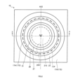
- FIG. 1 is a perspective view of a surface emitting laser of Example 1.
- FIG. 1 is a top view of a surface emitting laser of Example 1.
- FIG. 1 is a cross-sectional view of a surface emitting laser of Example 1.
- FIG. 10 is a top view of a surface-emitting laser of Modification 1;
- FIG. 11 is a cross-sectional view of a surface-emitting laser of Modification 2;
- FIG. 11 is a cross-sectional view of a surface-emitting laser according to Modification 3;
- FIG. 10 is a cross-sectional view of a surface-emitting laser of a modified example;
- FIG. 10 is a cross-sectional view of a surface-emitting laser of Example 2;
- FIG. 1 is a perspective view of a vertical cavity surface emitting laser (VCSEL: Vertical Cavity Surface Emitting Laser, hereinafter also simply referred to as a surface emitting laser) 10 according to Example 1.
- VCSEL Vertical Cavity Surface Emitting Laser
- the substrate 11 is a gallium nitride semiconductor substrate, such as an undoped GaN substrate.
- the substrate 11 is, for example, a substrate having a rectangular top surface shape.
- the upper surface of the substrate 11 is a plane that is 0.5° off from the C plane in the M plane direction. Further, the upper surface of the substrate 11 is hardly turned off from the C plane to the A plane direction, and the off angle from the C plane to the A plane direction is 0 ⁇ 0.01°.
- the axis that passes through the center of the top surface of the substrate 11 and is perpendicular to the top surface will be referred to as a central axis AX1.
- the substrate 11 is also arranged in the resonator, so it is preferable that the substrate 11 has high light transmittance. Therefore, the substrate 11 is preferably undoped.
- the convex portion 11P is a convex portion formed in a circular region centered on the central axis AX1 on the lower surface of the substrate 11 and having a downwardly convex curved surface.
- the convex portion 11P has a plano-convex lens shape.
- the optical axis of the lens shape formed by the convex portion 11P coincides with the central axis AX1.
- the back surface multilayer film reflector 12 (indicated by a two-dot chain line in the figure) is a dielectric multilayer film reflector made of a dielectric film formed on the surface of the convex portion 11P.
- the rear multilayer film reflector 12 is formed by alternately laminating a low refractive index dielectric film made of SiO 2 and a high refractive index dielectric film made of Nb 2 O 5 and having a higher refractive index than the low refractive index dielectric film. It is a dielectric multilayer reflector.
- the rear multilayer reflector 12 is a distributed Bragg reflector (DBR) made of a dielectric material.
- the rear multilayer reflector 12 is composed of four pairs of Nb 2 O 5 /SiO 2 layers formed on the surface of the convex portion 11P.
- a concave reflection structure 12R having an upward concave reflection surface 12RS is formed by the rear multilayer film reflector 12 and the convex portion 11P.
- the upper surface of the rear multilayer film reflector 12 is the concave reflecting surface 12RS.
- the first multilayer reflector 13 is a semiconductor multilayer reflector composed of semiconductor layers grown on the substrate 11 .
- a low refractive index semiconductor film having a composition of AlInN and a high refractive index semiconductor film having a GaN composition and having a higher refractive index than the low refractive index semiconductor film are alternately laminated. It is formed by In other words, the first multilayer reflector 13 is a distributed Bragg reflector (DBR) made of semiconductor material.
- DBR distributed Bragg reflector
- the first multilayer reflector 13 for example, a buffer layer having a GaN composition is provided on the upper surface of the substrate 11, and the high refractive index semiconductor film and the low refractive index semiconductor film are alternately formed on the buffer layer. formed by letting In this embodiment, the first multilayer reflector 13 consists of 35 pairs of GaN/AlInN layers laminated on a 1 ⁇ m thick GaN underlayer formed on the upper surface of the substrate 11 .
- the first multilayer film reflector 13 having such a structure has a reflectance of about 80% with respect to light emitted from the active layer 19 .
- the semiconductor structure layer 15 is a laminated structure composed of a plurality of semiconductor layers formed on the first multilayer reflector 13 .
- the semiconductor structure layer 15 includes an n-type semiconductor layer (first semiconductor layer) 17 formed on the first multilayer reflector 13 and a light-emitting layer (or active layer) formed on the n-type semiconductor layer 17. 19 and a p-type semiconductor layer (second semiconductor layer) 21 formed on the active layer 19 .
- the n-type semiconductor layer 17 as the first conductivity type semiconductor layer is a semiconductor layer formed on the first multilayer film reflector 13 .
- the n-type semiconductor layer 17 is a semiconductor layer having a GaN composition and being doped with Si as an n-type impurity.
- the n-type semiconductor layer 17 has a prismatic lower portion 17A and a cylindrical upper portion 17B disposed thereon.
- the n-type semiconductor layer 17 has a columnar upper portion 17B protruding from an upper surface 17S of a prismatic lower portion 17A.
- the n-type semiconductor layer 17 has a mesa-shaped structure including the upper portion 17B.
- the active layer 19 is formed on the upper portion 17B of the n-type semiconductor layer 17, and is a layer having a quantum well structure including well layers having an InGaN composition and barrier layers having a GaN composition. Light is generated in the active layer 19 in the surface emitting laser 10 .
- the active layer 19 is formed so that its emission center is brought on the central axis AX1.
- the p-type semiconductor layer 21 as the second conductivity type semiconductor layer is a semiconductor layer having a GaN composition formed on the active layer 19 .
- the p-type semiconductor layer 21 is doped with Mg as a p-type impurity.
- the n-electrode 23 is a metal electrode provided on the upper surface 17S of the lower portion 17A of the n-type semiconductor layer 17 and electrically connected to the n-type semiconductor layer 17.
- N-electrode 23 is formed in an annular shape so as to surround upper portion 17B of n-type semiconductor layer 17 .
- the n-electrode 23 is in electrical contact with the n-type semiconductor layer 17 and forms a first electrode layer that supplies current to the semiconductor structure layer 15 from the outside.
- the insulating layer 25 is a layer made of an insulator formed on the p-type semiconductor layer 21 .
- the insulating layer 25 is made of a material, such as SiO 2 , having a lower refractive index than the material forming the p-type semiconductor layer 21 .
- the insulating layer 25 is annularly formed on the p-type semiconductor layer 21 and has an opening (not shown) exposing the p-type semiconductor layer 21 in the central portion.
- the transparent electrode 27 is a transparent metal oxide film formed on the upper surface of the insulating layer 25 .
- the transparent electrode 27 covers the entire upper surface of the insulating layer 25 and the entire upper surface of the p-type semiconductor layer 21 exposed through the opening formed in the central portion of the insulating layer 25 .
- the metal oxide film that forms the transparent electrode 27 for example, ITO or IZO, which is transparent to the light emitted from the active layer 19, can be used.
- the p-electrode 29 is a metal electrode formed on the transparent electrode 27 .
- the p-electrode 29 is electrically connected via the transparent electrode 27 to the upper surface of the p-type semiconductor layer 21 exposed from the opening of the insulating layer 25 .
- the transparent electrode 27 and the p-electrode 29 form a second electrode layer that is in electrical contact with the p-type semiconductor layer 21 and supplies current to the semiconductor structure layer 15 from the outside.
- the p-electrode 29 is annularly formed on the upper surface of the transparent electrode 27 along the outer edge of the upper surface.
- the second multilayer reflector 31 is a cylindrical multilayer reflector formed in a region surrounded by the p-electrode 29 on the upper surface of the transparent electrode 27 .
- the second multilayer film reflector 31 is composed of a low refractive index dielectric film made of SiO2 and a high refractive index dielectric film made of Nb2O5 and having a higher refractive index than the low refractive index dielectric film . It is a laminated dielectric multilayer reflector.
- the second multilayer reflector 31 is a distributed Bragg reflector (DBR) made of dielectric material.
- DBR distributed Bragg reflector
- the second multilayer reflector 31 comprises a spacer layer of Nb 2 O 5 formed on the upper surface of the transparent electrode 27, and 10.5 pairs of Nb 2 O deposited on the spacer layer. 5 /SiO 2 layers.
- the second multilayer film reflector 31 having such a configuration has a reflectance of 99% or more with respect to light emitted from the active layer 19 .
- the reflectance of the second multilayer film reflector 31 is higher than the reflectance of the first multilayer film reflector 13 .
- FIG. 2 is a top view of the surface emitting laser 10.
- the axis along the m-axis direction in the same plane as the upper surface of the substrate 11 is defined as a lateral axis AX2.
- the surface-emitting laser 10 includes a semiconductor structure layer 15 including an n-type semiconductor layer 17 formed on a substrate 11 having a rectangular top surface, an active layer 19 having a circular top surface, and a p-type semiconductor layer 21 . (see FIG. 1).
- An insulating layer 25 and a transparent electrode 27 are formed on the p-type semiconductor layer 21 .
- a p-electrode 29 and a second multilayer film reflector 31 are formed on the transparent electrode 27 .
- the insulating layer 25 has an opening 25H which is a circular opening exposing the p-type semiconductor layer 21 of the insulating layer 25 described above. As shown in FIG. 2, the opening 25H is formed in the central portion of the insulating layer 25 when viewed from above the surface emitting laser 10, and is covered by the second multilayer reflector 31 when viewed from above the surface emitting laser 10. It is In other words, the opening 25 ⁇ /b>H is formed in a region of the insulating layer 25 facing the lower surface of the multilayer film reflector 31 . In this embodiment, the opening 25H has a diameter of 10 ⁇ m.
- the opening 25H has a circular shape centered on the central axis AX1. Therefore, the p-type semiconductor layer 21 is electrically connected to the transparent electrode 27 via the electrical contact surface 21S in the circular area exposed from the opening 25H on the upper surface of the p-type semiconductor layer 21.
- the convex portion 11P (thick dashed line in the figure) has a circular shape centered on the central axis AX1 when viewed from above.
- the convex portion 11P is formed over a region facing the electrical contact surface 21S on the lower surface of the substrate 11.
- the convex portion 11P is formed to overlap the electrical contact surface 21S when viewed from above, that is, in the normal direction of the upper surface of the substrate 11, and extends to the outside of the outer edge of the electrical contact surface 21S, ie, the outline.
- the convex portion 11P extends to the outside of the p-electrode 29, that is, to the outside of the upper portion 17B of the n-type semiconductor layer 17 when viewed from above.
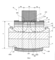
- FIG. 3 is a cross-sectional view of the surface emitting laser 10 taken along line 3-3 in FIG.
- the surface emitting laser 10 has the substrate 11 which is a GaN substrate, and the first multilayer reflector 13 is formed on the substrate 11 .
- the rear multilayer film reflector 12 is formed as the third multilayer film reflector. Therefore, the convex portion 11P and the rear multilayer reflector 12 form a concave reflection structure 12R having a concave reflecting surface facing the active layer 19 and the second multilayer reflector 31. As shown in FIG.
- the rear multilayer film reflector 12 has a function of concentrating the light that has passed through the first multilayer film reflector 13 and reached the rear multilayer film reflector 12 in a region along the central axis AX1.
- the semiconductor structural layer 15 is formed on the first multilayer reflector 13 .
- the semiconductor structure layer 15 is a laminate in which an n-type semiconductor layer 17, an active layer 19 and a p-type semiconductor layer 21 are formed in this order. At the center of the upper surface of the p-type semiconductor layer 21, a protruding portion 21P protruding upward is formed.
- the n-type semiconductor layer 17 is a 350 nm-thick n-GaN layer doped with Si.
- the active layer 19 has a multiple quantum well structure in which four pairs of 3 nm GaInN layers and 4 nm GaN layers are laminated.
- an undoped GaN layer with a thickness of 120 nm and an electron barrier layer of Mg-doped AlGaN (Al composition: 30%) with a thickness of 10 nm are formed.
- a p-type semiconductor layer 21 made of a p-GaN layer having a thickness is formed.
- the insulating layer 25 is formed so as to cover the region other than the protruding portion 21P on the upper surface of the p-type semiconductor layer 21 .
- the insulating layer 25 is made of a material having a lower refractive index than the p-type semiconductor layer 21 as described above.
- the insulating layer 25 has an opening 25H that exposes the protrusion 21P.
- the opening 25H and the protrusion 21P have the same shape, and the inner surface of the opening 25H and the outer surface of the protrusion 21P are in contact with each other.
- the insulating layer 25 is a layer of 20 nm SiO 2 .
- the upper surface of the insulating layer 25 is arranged at the same level as the upper surface of the protruding portion 21P of the p-type semiconductor layer 21 .
- the protruding portion 21P on the upper surface of the p-type semiconductor layer 21 protrudes from the surrounding area of the protruding portion 21P on the upper surface of the p-type semiconductor layer 21 by 20 nm. Therefore, the p-type semiconductor layer 21 has a layer thickness of 83 nm in the projecting portion 21P and a layer thickness of 63 nm in other regions.
- the transparent electrode 27 is formed so as to cover the upper surface of the insulating layer 25 and the protruding portion 21P exposed from the opening 25H of the insulating layer 25 . That is, the transparent electrode 27 is in electrical contact with the p-type semiconductor layer 21 in the region exposed through the opening 25H on the upper surface of the p-type semiconductor layer 21 . In other words, the region exposed through the opening 25H on the upper surface of the p-type semiconductor layer 21 serves as an electrical contact surface 21S that provides electrical contact between the p-type semiconductor layer 21 and the transparent electrode 27.
- the p-electrode 29 is a metal electrode as described above, and is formed along the outer edge of the top surface of the transparent electrode 27 . That is, the p-electrode 29 is in electrical contact with the transparent electrode 27 . Therefore, the p-electrode 29 is in electrical contact or connection with the p-type semiconductor layer 21 through the transparent electrode 27 at the electrical contact surface 21S exposed through the opening 25H on the upper surface of the p-type semiconductor layer 21.
- the second multilayer reflector 31 is located on the upper surface of the transparent electrode 27 and in the area above the opening 25H of the insulating layer 25, in other words, the area on the electrical contact surface 21S, that is, the central portion of the upper surface of the transparent electrode 27. formed.
- the lower surface of the second multilayer reflector 31 faces the upper surface of the first multilayer reflector 13 and the upper surface of the rear multilayer reflector 12 with the transparent electrode 27 and the semiconductor structure layer 15 interposed therebetween.
- a first resonator OC1 is formed between the first multilayer reflector 13 and the second multilayer reflector 31, and between the rear multilayer reflector 12 and the second multilayer reflector 31.
- a second resonator OC2 is formed.
- the resonator OC that resonates the light emitted from the active layer 19 includes the first resonator OC1 and the second resonator OC2.
- the reflectance of the second multilayer reflector 31 is slightly higher than the reflectance of the reflection structure composed of the back multilayer reflector 12 and the first multilayer reflector 13 . Therefore, part of the light resonating between the rear multilayer reflector 12 and the first multilayer reflector 13 and the second multilayer reflector 31 is transmitted through the first multilayer reflector 13 and the substrate 11 . and the rear multilayer film reflecting mirror 12, and taken out to the outside.
- the operation of the surface emitting laser 10 will be described.
- the surface-emitting laser 10 when a voltage is applied between the n-electrode 23 and the p-electrode 29, a current flows in the semiconductor structure layer 15 as indicated by the bold dashed-dotted arrow in the figure, and light is emitted from the active layer 19. is emitted.
- the light emitted from the active layer 19 is repeatedly reflected between the first multilayer reflector 13, the back multilayer reflector 12, and the second multilayer reflector 31, and reaches a resonance state (i.e., laser oscillation). do).
- the opening 25H has a current confinement structure that limits the current supply range in the active layer 19.
- FIG. That is, in the surface emitting laser, the p-type semiconductor layer 21 and the insulating layer 25 form a current confinement structure.
- a columnar region having the electrical contact surface 21S as a bottom surface is formed in the active layer 19 between the first multilayer reflector 13 and the second multilayer reflector 31.
- a current confinement structure is formed in which the current is confined to one region of the active layer so that the current flows only in the central region CA.
- a central region CA which includes a region through which current flows within the active layer 19, is defined by an electrical contact surface 21S.
- the first multilayer reflector 13 has a lower reflectance than the second multilayer reflector 31 . Therefore, part of the light coming from the second multilayer reflecting mirror 31 and the active layer 19 and reaching the first multilayer reflecting mirror 13 is transmitted to the rear multilayer reflecting mirror 12, and is transmitted to the second multilayer reflecting mirror 12. Resonance also occurs between the film reflecting mirror 31 and the rear multilayer film reflecting mirror 12 . A part of the resonated light is transmitted through the first multilayer film reflector 13, the back multilayer film reflector 12, and the substrate 11 and extracted to the outside.
- the surface emitting laser 10 emits light from the bottom surface of the substrate 11 in a direction perpendicular to the in-plane directions of the bottom surface of the substrate 11 excluding the protrusions 11P and the in-plane direction of each layer of the semiconductor structure layer 15 .
- the lower surface of the substrate 11 serves as the light emitting surface of the surface emitting laser 10 .
- the electrical contact surface 21S of the p-type semiconductor layer 21 of the semiconductor structure layer 15 and the opening 25H of the insulating layer 25 define the light emission center, which is the center of the light emission region in the active layer 19, and the central axis of the resonator OC. (luminescence central axis) is defined.
- the center axis of the resonator OC passes through the center of the electrical contact surface 21S of the p-type semiconductor layer 21 and extends along the direction perpendicular to the in-plane direction of the semiconductor structure layer 15 .
- the light emission central axis of the resonator OC is the same as the central axis AX1.
- the central axis AX1 is also referred to as the light emitting central axis AX1.
- the light emitting region of the active layer 19 is, for example, a region having a predetermined width from which light having a predetermined intensity or more is emitted in the active layer 19, the center of which is the light emitting center. Further, for example, the light emitting region of the active layer 19 is a region into which a current having a predetermined density or more is injected in the active layer 19, and the center thereof is the light emitting center. A straight line perpendicular to the in-plane direction of the upper surface of the substrate 11 or each layer of the semiconductor structure layer 15 passing through the center of light emission is the center axis of light emission AX1.
- the light emission central axis AX1 is a straight line extending along the cavity length direction of the cavity OC constituted by the first multilayer reflector 13, the back multilayer reflector 12, and the second multilayer reflector 31. . Also, the emission center axis AX1 corresponds to the optical axis of the laser light emitted from the surface emitting laser 10 .
- the insulating layer 25 has a lower refractive index than the p-type semiconductor layer 21 .
- the layer thicknesses of the active layer 19 and the n-type semiconductor layer 17 are set to any in-plane thickness. The locations are the same as long as they are in the same layer.
- the equivalent refractive index (back surface is the optical distance between the multilayer reflector 12 and the first multilayer reflector 13 and the second multilayer reflector 31 and corresponds to the resonance wavelength) is the p-type semiconductor layer 21 and the insulating layer 25 , the cylindrical central region CA having the electrical contact surface 21S as the bottom surface and the cylindrical peripheral region PA surrounding it.
- the equivalent refractive index of the peripheral area PA is lower than that of the central area CA. is also lower, ie the equivalent resonant wavelength in the central area CA is smaller than the equivalent resonant wavelength in the peripheral area PA.
- the light-emitting region from which light is emitted in the active layer 19 is the portion of the active layer 19 that overlaps with the central region CA, in other words, the region that overlaps with the electrical contact surface 21S when viewed from above.
- the central region CA including the light emitting region of the active layer 19 and the central region CA surrounding and surrounding the central region CA are formed by the p-type semiconductor layer 21 and the insulating layer 25 forming the current confining structure.
- a peripheral area PA having a lower refractive index than CA is formed.
- the p-type semiconductor layer 21 and the insulating layer 25 forming the current confinement structure also form a light confinement structure that confines light in the central region.
- the light that has passed through the first multilayer reflector 13 and reaches the rear multilayer reflector 12 is reflected by the concave reflecting structure 12 R formed by the rear multilayer reflector 12 . It is converged in the central area CA by the surface 12RS. That is, the light is confined in the central area CA also by the rear multilayer film reflecting mirror 12 .
- the resonator OC is formed by the rear multilayer reflector 12, the first multilayer reflector 13, and the second multilayer reflector 31, as described above.
- the rear multilayer reflector 12 is removed from the surface-emitting laser 10 of the present application, and the reflectances of the first multilayer reflector 13 and the second multilayer reflector 31 are made close to form a resonator alone.
- a configuration hereinafter also referred to as a comparative configuration.
- the diameter of the opening 25H that forms the current confining structure that limits the flow of current into the active layer 19 and defines the light emitting region is about 5.5 .mu.m or less, the extracted light is unlikely to be single mode. It has been found by the inventors of the present application.
- the current injection region had to be kept small in the case of a comparative configuration in which light was confined simply by a structure forming a current confinement structure and the transverse mode was controlled to a single mode. This is because when the current injection region of the active layer is increased to increase the optical output, spatial hole burning occurs near the emission center of the active layer, resulting in a decrease in optical gain near the emission center.
- This spatial hole burning is a phenomenon in which the light density is excessively increased in a specific region of the active layer, resulting in a large amount of stimulated emission, and the injected carriers are consumed in the region where the light density is high, resulting in a decrease in carrier density. is.
- the opening 25H is made larger than 5.5 ⁇ m in order to increase the light output
- the light confinement effect caused by the current confinement structure causes the light to concentrate too much around the emission center of the active layer.
- the light density becomes excessively high, and hole burning occurs.
- the optical gain of the cavity in the width direction will have a plurality of peaks, and the transverse modes of the extracted light will be multiple modes.
- the rear multilayer reflecting mirror 12 and the first multilayer reflecting mirror 13 form a reflecting structure for reflecting light upward
- the second multilayer reflecting mirror 31 form a reflecting structure that reflects light downward, and these form a resonator.
- part of the light from the first resonator OC1 composed of the first multilayer reflector 13 and the second multilayer reflector 31 is transmitted to the first multilayer reflector. 13 and directed downward.
- a second resonator OC2 is also formed between the second multilayer reflector 31 and the rear multilayer reflector 12 having the concave reflecting surface 12RS that reflects while converging toward the central axis AX1.
- the luminous center It is possible to reduce the light density in the region around the axis AX1 and suppress the occurrence of spatial hole burning.
- the surface emitting laser 10 not only the light confining structure formed between the first multilayer reflector 13 and the second multilayer reflector 31 but also the rear multilayer reflector 12 It has another lateral light confinement structure that concentrates light in the central area CA. Moreover, since the reflectance of the first multilayer film reflector 13 is low as described above, the first resonator between the first multilayer film reflector 13 and the second multilayer film reflector 31 The light confinement effect by the current confinement structure, which is strongly generated in OC1, becomes milder than in the conventional case.
- the optical confinement effect by the current confinement structure causes resonance only in the first resonator OC1 between the first multilayer reflector 13 and the second multilayer reflector 31. It becomes looser than the comparative configuration. Instead, the rear multilayer reflector 12 having a concave reflecting surface 12RS that reflects the light passing through the first multilayer reflector 13 and directed downward while converging upward toward the central axis AX1, It is in the form of compensating for the light confinement effect by the current confinement structure that has become moderate.
- the surface-emitting laser 10 hole burning does not occur even if the current injection region of the active layer 19 is enlarged by enlarging the opening 25H, and the light intensity distribution of the emitted light can easily maintain the Gaussian distribution. . That is, in the surface-emitting laser 10, the transverse mode of the emitted light is likely to be maintained in a single mode.
- the curvature radius R of the concave reflecting surface 12RS of the concave reflecting structure 12R preferably satisfies the following formula (1).
- Z is originally the distance between the reflecting surface of the concave reflecting structure and the active layer 19, but since the distance between the active layer 19 and the lower surface of the second multilayer film reflecting mirror 31 is small enough to approximate, It is the distance between the reflecting surface of the reflecting structure 12R and the lower surface of the second multilayer film reflecting mirror 31 (see FIG. 3).
- n eq is the equivalent refractive index of the semiconductor between the reflecting surface of the concave reflecting structure 12R and the lower surface of the second multilayer reflector 31;
- This relationship is derived from the position of 1/e of the light intensity at the peak from the position of the peak in the light intensity distribution in the plane perpendicular to the emission direction of the light emitted from the surface-emitting laser 10 in the first cavity OC1.
- ⁇ 0 which is the distance to , i.e., 1/2 of the beam spot diameter, and Eq. (2) below.
- the above formula (1) is derived from the above formula (2) showing the relationship between ⁇ 0 and R. Specifically, the condition is that the spot diameter ⁇ 0 of the light output from the first resonator OC1 is 1.65 ⁇ m at maximum, and the spot diameter of the light output from the second resonator OC2 is less than this. It is derived by introducing the condition that it is preferable to be large into the above formula (1).
- the upper surface of the substrate 11 is a plane that is 0.5° off from the C-plane in the M-plane direction.
- the optical gain of the light having the polarization direction in the m-axis direction is changed to the other direction.
- the laser light having the polarization direction in the m-axis direction easily oscillates. Therefore, most of the light emitted from the central region CA of the surface emitting laser 10 has the polarization direction in the m-axis direction. That is, the surface-emitting laser 10 emits more light that has a polarization direction along the horizontal axis AX2.
- the surface emitting laser of the present invention it becomes easy to increase the emission output while maintaining the transverse mode of the emitted light in the single mode. In addition, it has high luminous efficiency, and it is possible to stably obtain emitted light in a specific polarization direction. This is very effective when the light emitted from the surface emitting laser is used in a device having an optical system using liquid crystals or polarizers.
- a GaN substrate whose upper surface is a crystal plane inclined from the C plane to the M plane is prepared as described above.
- a GaN layer (thickness: 1 ⁇ m) is formed as a base layer on the upper surface of the substrate 11 by metal-organic vapor phase epitaxy (MOVPE). After that, 35 pairs of n-GaN/AlInN layers are formed on the underlying layer to form the first multilayer reflector 13 .
- MOVPE metal-organic vapor phase epitaxy
- Si-doped n-GaN (layer thickness: 350 nm) is formed on the first multilayer reflector 13 to form an n-type semiconductor layer 17, and GaInN (layer thickness: 3 nm) and GaN (layer thickness: 3 nm) are formed thereon.
- the active layer 19 is formed by laminating four pairs of layers each having a layer thickness of 4 nm).
- the surrounding portions of the p-type semiconductor layer 21, the active layer 19 and the n-type semiconductor layer 17 are etched to form a mesa shape in which the upper surface 17S of the n-type semiconductor layer 17 is exposed in the surrounding portions.
- the semiconductor structure layer 15 having a columnar portion composed of the n-type semiconductor layer 17, the active layer 19 and the p-type semiconductor layer 21 shown in FIG. 1 is completed.
- the periphery of the central portion of the upper surface of the p-type semiconductor layer 21 is etched to form a protruding portion 21P.
- an insulating layer 25 is formed by forming a film of SiO 2 to a thickness of 20 nm on the semiconductor structure layer 15 and partially removing it to form an opening 25H. In other words, SiO 2 is buried in the etched away portion of the upper surface of the p-type semiconductor layer 21 .
- an ITO film having a thickness of 20 nm is formed on the insulating layer 25 to form a transparent electrode 27, and an Au film is formed on the upper surface of the transparent electrode 27 and the upper surface 17S of the n-type semiconductor layer 17 to form a p-electrode 29 and an n-electrode. 23 is formed.
- a 38 nm Nb 2 O 5 film is formed on the transparent electrode 27 as a spacer layer (not shown).
- a pair of films are formed to form the second multilayer film reflector 31 .
- the convex portion 11P is formed on the back surface of the substrate 11 .
- the convex portion 11P is formed by a reflow process such that the center axis of the lens shape coincides with the light emission center axis AX1. Note that the convex portion 11P may be formed using exposure patterning and dry etching.
- a resist is deposited on the back surface of the substrate 11 in the same shape as the projections 11P, the entire back surface of the substrate 11 is dry-etched, and the shape of the resist is transferred to the back surface of the substrate 11. You may form the convex part 11P by this.
- Modification 1 A surface-emitting laser 40, which is a first modification of the surface-emitting laser 10 according to the first embodiment of the present invention, will be described below. Modification 1 differs from the surface emitting laser 10 in that the convex portion 11P is not circular, that is, the concave reflecting surface formed by the concave reflecting structure 12R is not circular.
- FIG. 4 is a top view of the surface-emitting laser 40 of Modification 1.
- the top surface shape of the convex portion 11P has an elliptical shape whose major axis is in the same direction as the lateral axis AX2. That is, the convex portion 11P has an elliptical upper surface shape having a major axis along the m-axis direction when viewed from above.
- the convex portion 11P has an elliptical shape with a long axis in the m-axis direction
- the reflecting surface of the concave reflecting structure 12R has an elliptical upper surface shape with a long axis in the m-axis direction. Then, in the central area CA of the light polarized along the m-axis, the optical gain of the light polarized along the m-axis increases and the loss in the m-axis decreases. , was discovered by the inventor of the present invention.
- the surface-emitting laser 40 a large amount of light having a polarization direction along the m-axis can be extracted from the lower surface of the substrate 11, which is the light emitting surface of the surface-emitting laser 10, and Emission of light having a polarization direction other than the parallel direction can be suppressed. Therefore, according to the surface emitting laser 40, it is possible to further suppress variations in the polarization direction of the light extracted from the light emitting surface in the in-plane direction of the light emitting surface.
- the shape of the convex portion 11P for further suppressing the variation in the polarization direction in other words, the shape of the upper surface of the reflecting surface of the concave reflecting structure 12R may be any shape as long as the direction along the lateral axis AX2 is the longitudinal direction. may be in the shape of In other words, the shape of the upper surface of the convex portion 11P may be any shape other than an ellipse as long as it has a longitudinal direction along the horizontal axis AX2.
- the shape of the upper surface of the convex portion 11P may be rectangular or rectangular with the longitudinal direction along the lateral axis AX2. Further, for example, the shape of the upper surface of the convex portion 11P may be an elliptical shape having the same contour as that of a land track whose longitudinal direction is along the direction of the lateral axis AX2. Further, for example, the shape of the upper surface of the convex portion 11P may be a diamond shape whose longitudinal direction is along the direction of the axis AX2.
- a surface-emitting laser 50 which is a modification 2 of the surface-emitting laser 10 of the first embodiment of the present invention, will be described below with reference to FIG.
- the surface-emitting laser 50 of Modification 2 differs from the surface-emitting laser 10 of Example 1 in that the rear multilayer reflector 12 is not formed.
- FIG. 5 is a cross-sectional view showing a cut surface when the surface-emitting laser 50 is cut along the same cutting line as shown in FIG. 2, that is, a cut surface corresponding to FIG.
- the surface-emitting laser 50 does not have the rear multilayer film reflector 12, but has a diffraction grating 53 (inside the dashed line in the figure) made up of a plurality of slit grooves 51 on the surface of the convex portion 11P. formed. That is, the convex portion 11P and the diffraction grating 53 form a concave reflecting structure 55R having a concave reflecting surface 55RS.
- the slit groove 51 has its longitudinal direction in the same direction as the lateral axis AX2 (see FIG. 2), which is the axis along the direction perpendicular to the paper surface of FIG. That is, the slit groove 51 has a longitudinal direction along the m-axis direction when viewed from above.
- the diffraction grating 53 formed by the slit grooves 51 provides a high reflectance for light whose polarization direction is the extension direction of each of the slit grooves 51 forming the diffraction grating, that is, the m-axis direction. That is, since the diffraction grating 53 made up of the slit grooves 51 is formed, the reflectance of the light whose polarization direction is the m-axis direction is higher than that of light having other polarization directions, and the m-axis direction is the polarization direction.
- the light that is set to is preferentially easier to oscillate.
- the diffraction grating 53 made up of the slit grooves 51 is formed on the lower surface of the substrate 11 to form the concave reflection structure 55R, thereby further controlling the polarization of the emitted light. It is possible to stably obtain emitted light in which directional light is dominant.
- the slit grooves 51 can be formed by performing an etching process such as dry etching on the lower surface of the substrate 11 in the final step of manufacturing the surface emitting laser 10 of the first embodiment described above.
- a surface-emitting laser 60 that is a third modification of the first embodiment of the present invention will be described below with reference to FIG.
- the surface emitting laser 60 differs from the surface emitting laser 10 of Example 1 in that a tunnel junction structure is formed in the semiconductor structure layer 15 instead of the insulating layer 25 in order to form the above-described current confinement structure.
- the surface emitting laser 60 differs from the surface emitting laser 10 in the structure above the p-type semiconductor layer 21 .
- FIG. 6 is a cross-sectional view showing a cut surface when the surface-emitting laser 60 is cut along the same cutting line as shown in FIG. 2, that is, a cut surface corresponding to FIG.
- a tunnel junction layer 61 is formed on the projecting portion 21P of the p-type semiconductor layer 21.
- a tunnel junction layer 61 is formed in the central region CA within the semiconductor structure layer 15 .
- the tunnel junction layer 61 is formed on the p-type semiconductor layer 21 and includes a highly doped p-type semiconductor layer 61A, which is a p-type semiconductor layer having an impurity concentration higher than that of the p-type semiconductor layer 21, and on the highly doped p-type semiconductor layer 61A. and a highly doped n-type semiconductor layer 61 ⁇ /b>B, which is an n-type semiconductor layer having an impurity concentration higher than that of the n-type semiconductor layer 17 .
- the n-type semiconductor layer 63 is formed on the p-type semiconductor layer 21 and the tunnel junction layer 61 .
- the n-type semiconductor layer 63 is formed to bury the tunnel junction layer 61 on the upper surface of the p-type semiconductor layer 21 .
- the n-type semiconductor layer 63 is formed to cover the side surfaces of the protruding portion 21 ⁇ /b>P and the side surfaces and upper surface of the tunnel junction layer 61 .
- the second multilayer reflector 65 is formed on the upper surface of the n-type semiconductor layer 63 and is an n-type semiconductor layer having the same doping concentration as the n-type semiconductor layer 17 . That is, the n-type semiconductor layer 63 has a doping concentration lower than that of the highly doped n-type semiconductor layer 61B.
- the tunnel junction layer 61 and the n-type semiconductor layer 63 Due to such a laminated structure of the p-type semiconductor layer 21, the tunnel junction layer 61 and the n-type semiconductor layer 63, a tunnel effect occurs in the tunnel junction layer 61 portion. As a result, in the surface-emitting laser 60, between the p-type semiconductor layer 21 and the n-type semiconductor layer 63, a current flows only through the tunnel junction layer 61, and a current is confined in the central region CA. It is formed.
- the second multilayer reflector 65 is a semiconductor multilayer reflector comprising a semiconductor layer formed on the n-type semiconductor layer 63 .
- a low refractive index semiconductor film having a composition of AlInN and a high refractive index semiconductor film having a GaN composition and having a higher refractive index than the low refractive index semiconductor film are alternately laminated. and has the characteristics of an n-type semiconductor.
- the second multilayer reflector 65 is a distributed Bragg reflector (DBR) made of semiconductor material.
- DBR distributed Bragg reflector
- the p-side electrode 67 is a metal electrode formed along the periphery of the top surface of the second multilayer film reflector 65 .
- the second multilayer reflector 65 is conductive, from the p-side electrode 67, the second multilayer reflector 65, the n-type semiconductor layer 63, the tunnel junction layer 61, the p-type semiconductor A current flows through layer 21 , active layer 19 and n-type semiconductor layer 17 to n-electrode 23 .
- the tunnel junction layer 61 that forms a tunnel junction in the same region as the electrical contact surface 21S when viewed from above, the same current constriction effect as the electrical contact surface 21S is formed. , a light confinement effect can be obtained.
- the n-electrode 23 is formed on the n-type semiconductor layer 17 in the first embodiment and modified examples 1 to 3 above, the n-side electrode may be formed on the rear surface of the substrate 11 instead.
- FIG. 7 shows a case where an n-side electrode 68 is formed in the region around the convex portion 11P, that is, in the region outside the concave reflecting structure 12R, instead of the n-electrode 23 in the surface emitting laser 10 of the first embodiment.
- a cross-sectional view is shown.
- the substrate 11 must be doped because the substrate 11 serves as a current path.
- the substrate 11 is also arranged in the resonator, so it is preferable that the substrate 11 has high light transmittance. Therefore, the n-type dopant with which the substrate 11 is doped is preferably Si rather than oxygen, and the dopant concentration is preferably low.
- the n-type dopant with which the substrate 11 is doped is preferably Si rather than oxygen, and the dopant concentration is preferably low.
- the substrate 11 it is preferable that 80% of the regions in the first resonator OC1 and the second resonator OC2 have a Si dopant concentration of 2 ⁇ 10 18 /cm 3 or less.
- the area of 1 ⁇ 10 18 /cm 3 or less occupies 80%.
- the portion where the n-side electrode is formed needs to have a high dopant concentration.
- the substrate 11 satisfying the above dopant concentration condition is formed.
- oxygen may be used as the dopant for the portion where the n-side electrode is to be formed, since it is a region outside the resonator OC.
- FIG. 8 is a cross-sectional view showing a cut surface when the surface-emitting laser 79 is cut along the same cutting line as shown in FIG. 2, that is, a cut surface corresponding to FIG.
- a concave reflecting structure 71R having a concave reflecting surface 71RS is provided below the substrate 11.
- the forming output coupler 71 is arranged. In other words, the output coupler 71 is spaced below the substrate 11 .
- the output coupler 71 consists of a transparent substrate 72 having a concave surface 72S facing the lower surface of the substrate 11 and an external multilayer reflector 73 which is a dielectric DBR covering the concave surface 72S.
- a concave reflecting structure 71 R corresponding to the concave reflecting structure 12 R of the surface emitting laser 10 is formed by the transparent substrate 72 and the external multilayer film reflector 73 .
- a second resonator OC2 is formed between the second multilayer reflector 31 and the external multilayer reflector 73. As shown in FIG.
- the rear surface of the substrate 11 is formed with, for example, four pairs of AR coats of Nb 2 O 5 /SiO 2 so that the rear surface of the substrate 11 does not reflect light.
- Such a configuration using the output coupler 71 instead of the concave reflecting structure 12R formed by the convex portion 11P formed on the lower surface of the substrate 11 is used when the concave reflecting structure 12R has to be enlarged in the surface emitting laser 10 from the design point of view.
- This configuration is advantageous for
- the concave reflection structure 12R when a large number of surface-emitting lasers 10 are formed on a wafer and separated into individual pieces, if the concave reflection structure 12R must be enlarged, the number of surface-emitting lasers 10 to be manufactured per wafer is reduced to the convex portion. It may be limited by the size of 11P. In such a case, by replacing the concave reflecting structure 12R with the concave reflecting structure 71R of the external output coupler 71, it is possible to increase the size of the concave reflecting structure without reducing the number of surface emitting lasers manufactured per wafer. can.
- the upper surface of the substrate 11 is 0.5° off from the C plane in the direction of the M plane, that is, when the off angle from the C plane to the direction of the M plane is 0.5°.
- the off angle is not limited to this angle. If the off angle is, for example, about 0.3° to 0.8°, the above-described polarization control effect can be sufficiently obtained. Further, when the off-angle of the upper surface of the substrate 11 is 0.8° or less, the semiconductor multilayer film constituting the first multilayer reflector 13 can be stably formed to have a sufficient reflectance. .
- the upper surface of the substrate 11 is turned off in the direction of the M plane from the C plane. It does not have to be almost off in the direction.
- the off angle from the C plane to the A plane direction is about 0.3° to 0.8° for the same reason as the explanation about the range of the off angle of the C plane. and the off angle from the C plane to the M plane is preferably 0 ⁇ 0.1°.
- the longitudinal direction of the upper surface shape of the protrusion 11P in Modification 1 and the longitudinal direction of the slit groove 51 in Modification 2 are described in the lateral direction. It should be understood by rereading that the axis AX2 corresponds to the a axis.
- the upper surface of the substrate 11 When the upper surface of the substrate 11 is turned off from the C plane to the A plane direction, a large amount of light having a polarization direction along the a-axis direction can be extracted, and light having a polarization direction other than the direction along the a-axis can be extracted. emission can be suppressed. Therefore, according to the surface emitting laser 10, it is possible to suppress variations in the polarization direction of the light extracted from the light emitting surface in the in-plane direction of the light emitting surface.
- the substrate 11 may be a C-plane substrate in which the C-plane is exposed on the upper surface.
Landscapes
- Physics & Mathematics (AREA)
- Condensed Matter Physics & Semiconductors (AREA)
- General Physics & Mathematics (AREA)
- Electromagnetism (AREA)
- Optics & Photonics (AREA)
- Semiconductor Lasers (AREA)
Priority Applications (1)
| Application Number | Priority Date | Filing Date | Title |
|---|---|---|---|
| US18/842,138 US20250392103A1 (en) | 2022-03-01 | 2023-02-22 | Vertical cavity light-emitting element |
Applications Claiming Priority (2)
| Application Number | Priority Date | Filing Date | Title |
|---|---|---|---|
| JP2022030773A JP2023127163A (ja) | 2022-03-01 | 2022-03-01 | 垂直共振器型発光素子 |
| JP2022-030773 | 2022-03-01 |
Publications (1)
| Publication Number | Publication Date |
|---|---|
| WO2023167076A1 true WO2023167076A1 (ja) | 2023-09-07 |
Family
ID=87883581
Family Applications (1)
| Application Number | Title | Priority Date | Filing Date |
|---|---|---|---|
| PCT/JP2023/006504 Ceased WO2023167076A1 (ja) | 2022-03-01 | 2023-02-22 | 垂直共振器型発光素子 |
Country Status (3)
| Country | Link |
|---|---|
| US (1) | US20250392103A1 (https=) |
| JP (1) | JP2023127163A (https=) |
| WO (1) | WO2023167076A1 (https=) |
Citations (7)
| Publication number | Priority date | Publication date | Assignee | Title |
|---|---|---|---|---|
| JP2001168461A (ja) * | 1999-10-01 | 2001-06-22 | Fuji Xerox Co Ltd | 面発光型半導体レーザ及びレーザアレイ |
| US20020176473A1 (en) * | 2001-05-23 | 2002-11-28 | Aram Mooradian | Wavelength selectable, controlled chirp, semiconductor laser |
| JP2011096856A (ja) * | 2009-10-29 | 2011-05-12 | Sony Corp | 半導体レーザ |
| JP2013229580A (ja) * | 2012-03-22 | 2013-11-07 | Palo Alto Research Center Inc | 第3の反射器を組み込んだ面発光レーザ |
| JP2016086156A (ja) * | 2014-10-22 | 2016-05-19 | 株式会社東芝 | 光学デバイスおよび光学デバイスを製造する方法 |
| JP2020188206A (ja) * | 2019-05-16 | 2020-11-19 | スタンレー電気株式会社 | 垂直共振器型面発光素子 |
| US20210399522A1 (en) * | 2020-06-23 | 2021-12-23 | Hewlett Packard Enterprise Development Lp | Coupled-cavity vcsels for enhanced modulation bandwidth |
-
2022
- 2022-03-01 JP JP2022030773A patent/JP2023127163A/ja active Pending
-
2023
- 2023-02-22 WO PCT/JP2023/006504 patent/WO2023167076A1/ja not_active Ceased
- 2023-02-22 US US18/842,138 patent/US20250392103A1/en active Pending
Patent Citations (7)
| Publication number | Priority date | Publication date | Assignee | Title |
|---|---|---|---|---|
| JP2001168461A (ja) * | 1999-10-01 | 2001-06-22 | Fuji Xerox Co Ltd | 面発光型半導体レーザ及びレーザアレイ |
| US20020176473A1 (en) * | 2001-05-23 | 2002-11-28 | Aram Mooradian | Wavelength selectable, controlled chirp, semiconductor laser |
| JP2011096856A (ja) * | 2009-10-29 | 2011-05-12 | Sony Corp | 半導体レーザ |
| JP2013229580A (ja) * | 2012-03-22 | 2013-11-07 | Palo Alto Research Center Inc | 第3の反射器を組み込んだ面発光レーザ |
| JP2016086156A (ja) * | 2014-10-22 | 2016-05-19 | 株式会社東芝 | 光学デバイスおよび光学デバイスを製造する方法 |
| JP2020188206A (ja) * | 2019-05-16 | 2020-11-19 | スタンレー電気株式会社 | 垂直共振器型面発光素子 |
| US20210399522A1 (en) * | 2020-06-23 | 2021-12-23 | Hewlett Packard Enterprise Development Lp | Coupled-cavity vcsels for enhanced modulation bandwidth |
Also Published As
| Publication number | Publication date |
|---|---|
| JP2023127163A (ja) | 2023-09-13 |
| US20250392103A1 (en) | 2025-12-25 |
Similar Documents
| Publication | Publication Date | Title |
|---|---|---|
| JP7754653B2 (ja) | 垂直共振器型発光素子 | |
| JP7453489B2 (ja) | 波長変換装置及び発光装置 | |
| CN112913094B (zh) | 垂直谐振器式发光元件 | |
| US20250158360A1 (en) | Vertical cavity surface emitting device | |
| JP4233366B2 (ja) | 光ポンピング可能な垂直エミッタを有する面発光半導体レーザ装置 | |
| CN101641847A (zh) | 光子晶体激光器及其制造方法 | |
| US20060088072A1 (en) | Semiconductor laser apparatus | |
| CN114051682B (zh) | 垂直腔面发光器件 | |
| JP7795900B2 (ja) | 垂直共振器型発光素子 | |
| JP7810774B2 (ja) | 垂直共振器型発光素子 | |
| US20240380173A1 (en) | Vertical cavity light-emitting element | |
| JP2017204579A (ja) | 垂直共振器型発光素子及び垂直共振器型発光素子の製造方法 | |
| JP3932466B2 (ja) | 半導体レーザ | |
| WO2023167076A1 (ja) | 垂直共振器型発光素子 | |
| US20250266664A1 (en) | Semiconductor laser element | |
| JP2003332684A (ja) | 面発光レーザ素子 | |
| JPH01308091A (ja) | 面発光型半導体レーザ装置 |
Legal Events
| Date | Code | Title | Description |
|---|---|---|---|
| 121 | Ep: the epo has been informed by wipo that ep was designated in this application |
Ref document number: 23763335 Country of ref document: EP Kind code of ref document: A1 |
|
| NENP | Non-entry into the national phase |
Ref country code: DE |
|
| 122 | Ep: pct application non-entry in european phase |
Ref document number: 23763335 Country of ref document: EP Kind code of ref document: A1 |