WO2023162964A1 - 光回路基板 - Google Patents
光回路基板 Download PDFInfo
- Publication number
- WO2023162964A1 WO2023162964A1 PCT/JP2023/006186 JP2023006186W WO2023162964A1 WO 2023162964 A1 WO2023162964 A1 WO 2023162964A1 JP 2023006186 W JP2023006186 W JP 2023006186W WO 2023162964 A1 WO2023162964 A1 WO 2023162964A1
- Authority
- WO
- WIPO (PCT)
- Prior art keywords
- core
- optical
- circuit board
- optical component
- clad
- Prior art date
- Legal status (The legal status is an assumption and is not a legal conclusion. Google has not performed a legal analysis and makes no representation as to the accuracy of the status listed.)
- Ceased
Links
Images



Classifications
-
- G—PHYSICS
- G02—OPTICS
- G02B—OPTICAL ELEMENTS, SYSTEMS OR APPARATUS
- G02B6/00—Light guides; Structural details of arrangements comprising light guides and other optical elements, e.g. couplings
- G02B6/24—Coupling light guides
- G02B6/42—Coupling light guides with opto-electronic elements
-
- G—PHYSICS
- G02—OPTICS
- G02B—OPTICAL ELEMENTS, SYSTEMS OR APPARATUS
- G02B6/00—Light guides; Structural details of arrangements comprising light guides and other optical elements, e.g. couplings
- G02B6/10—Light guides; Structural details of arrangements comprising light guides and other optical elements, e.g. couplings of the optical waveguide type
- G02B6/12—Light guides; Structural details of arrangements comprising light guides and other optical elements, e.g. couplings of the optical waveguide type of the integrated circuit kind
-
- G—PHYSICS
- G02—OPTICS
- G02B—OPTICAL ELEMENTS, SYSTEMS OR APPARATUS
- G02B6/00—Light guides; Structural details of arrangements comprising light guides and other optical elements, e.g. couplings
- G02B6/10—Light guides; Structural details of arrangements comprising light guides and other optical elements, e.g. couplings of the optical waveguide type
- G02B6/12—Light guides; Structural details of arrangements comprising light guides and other optical elements, e.g. couplings of the optical waveguide type of the integrated circuit kind
- G02B6/13—Integrated optical circuits characterised by the manufacturing method
- G02B6/138—Integrated optical circuits characterised by the manufacturing method by using polymerisation
-
- G—PHYSICS
- G02—OPTICS
- G02B—OPTICAL ELEMENTS, SYSTEMS OR APPARATUS
- G02B6/00—Light guides; Structural details of arrangements comprising light guides and other optical elements, e.g. couplings
- G02B6/24—Coupling light guides
- G02B6/42—Coupling light guides with opto-electronic elements
- G02B6/4201—Packages, e.g. shape, construction, internal or external details
- G02B6/4204—Packages, e.g. shape, construction, internal or external details the coupling comprising intermediate optical elements, e.g. lenses, holograms
- G02B6/4214—Packages, e.g. shape, construction, internal or external details the coupling comprising intermediate optical elements, e.g. lenses, holograms the intermediate optical element having redirecting reflective means, e.g. mirrors, prisms for deflecting the radiation from horizontal to down- or upward direction toward a device
-
- G—PHYSICS
- G02—OPTICS
- G02B—OPTICAL ELEMENTS, SYSTEMS OR APPARATUS
- G02B6/00—Light guides; Structural details of arrangements comprising light guides and other optical elements, e.g. couplings
- G02B6/24—Coupling light guides
- G02B6/42—Coupling light guides with opto-electronic elements
- G02B6/4201—Packages, e.g. shape, construction, internal or external details
- G02B6/4219—Mechanical fixtures for holding or positioning the elements relative to each other in the couplings; Alignment methods for the elements, e.g. measuring or observing methods especially used therefor
- G02B6/4236—Fixing or mounting methods of the aligned elements
- G02B6/424—Mounting of the optical light guide
-
- G—PHYSICS
- G02—OPTICS
- G02B—OPTICAL ELEMENTS, SYSTEMS OR APPARATUS
- G02B6/00—Light guides; Structural details of arrangements comprising light guides and other optical elements, e.g. couplings
- G02B6/24—Coupling light guides
- G02B6/42—Coupling light guides with opto-electronic elements
- G02B6/43—Arrangements comprising a plurality of opto-electronic elements and associated optical interconnections
Definitions
- the present invention relates to an optical circuit board and an optical component mounting structure using the same.
- optical fibers that can transmit large amounts of data at high speed have been used for information communication.
- Optical signals are transmitted and received between the optical fiber and the optical component.
- Such an optical component is mounted on an optical circuit board as described in Patent Document 1, for example.
- An optical circuit board includes a wiring board having an upper surface including a first mounting area and a second mounting area adjacent to the first mounting area, and an optical waveguide located in the first mounting area.
- the optical waveguide includes a first lower clad, a first core and a first upper clad from the upper surface side of the wiring substrate.
- the first lower cladding includes a first portion located in the first mounting area and a second portion located in the second mounting area. The first portion and the second portion have the same height.
- An optical component mounting structure includes the optical circuit board described above and an optical component located in the second mounting area.
- An optical component has an optical transmission line including a second upper clad, a second core and a second lower clad from the upper surface side of the wiring board.
- the second core includes a linear portion and a planar portion.
- the second upper clad When viewed from the wiring board side, the second upper clad has a recess having a planar portion as a bottom at a position overlapping the second portion. The planar portion located on the bottom and the second portion are in contact.
- FIG. 1 is a plan view showing an optical component mounting structure in which optical components and electronic components are mounted on an optical circuit board according to an embodiment of the present disclosure
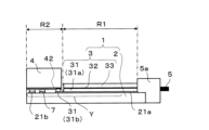
- FIG. 2 is an enlarged explanatory view for explaining a cross section of a region X shown in FIG. 1
- FIG. FIG. 3 is a plan view of a region Y shown in FIG. 2 (excluding optical components)
- 1 is an explanatory diagram of an example of an optical component mounted on an optical circuit board according to an embodiment of the present disclosure, viewed from the wiring board side
- FIG. FIG. 4 is an explanatory diagram for explaining a process of manufacturing an optical circuit board according to an embodiment of the present disclosure
- 4 is an enlarged explanatory view for explaining a cross section of a region Z1 shown in FIG.
- FIG. 4 is an enlarged explanatory view for explaining a cross section of a region Z2 shown in FIG. 3 when an optical component is mounted on the optical circuit board according to the embodiment of the present disclosure
- FIG. 5 is a plan view for explaining another form in which an optical component is mounted on an optical circuit board according to an embodiment of the present disclosure
- FIG. 9 is an enlarged explanatory view for explaining cross sections of regions Z3 and Z4 shown in FIG. 8 in another form in which optical components are mounted on the optical circuit board according to the embodiment of the present disclosure
- the first lower clad has a first portion located in the first mounting region and a second portion located in the second mounting region. two portions, the first portion and the second portion having the same height.
- FIG. 1 is a plan view showing an optical component mounting structure 10 in which optical components 4 and electronic components 6 are mounted on an optical circuit board 1 according to an embodiment of the present disclosure.
- An optical circuit board 1 includes a wiring board 2 and an optical waveguide 3.
- a wiring board 2 included in the optical circuit board 1 according to one embodiment, a wiring board generally used for an optical circuit board can be used.
- such a wiring board 2 includes, for example, a core board and buildup layers laminated on both sides of the core board.
- the core substrate is not particularly limited as long as it is an insulating material. Examples of insulating materials include resins such as epoxy resins, bismaleimide-triazine resins, polyimide resins, and polyphenylene ether resins. These resins may be used in combination of two or more.
- the core substrate usually has through-hole conductors for electrically connecting the upper and lower surfaces of the core substrate.
- the core substrate may contain a reinforcing material.
- reinforcing materials include insulating cloth materials such as glass fibers, glass nonwoven fabrics, aramid nonwoven fabrics, aramid fibers, and polyester fibers. Two or more reinforcing materials may be used in combination.
- inorganic fillers such as silica, barium sulfate, talc, clay, glass, calcium carbonate, and titanium oxide may be dispersed in the core substrate.
- the buildup layer has a structure in which insulating layers and conductor layers are alternately laminated.
- a part of the conductor layer positioned on the outermost surface (the conductor layer positioned on the upper surface of the wiring board 2) includes a conductor layer 21a on which the optical waveguide 3 is positioned.
- the conductor layer 21a is made of metal such as copper.
- the insulating layer included in the buildup layer is not particularly limited as long as it is an insulating material, like the core substrate. Examples of insulating materials include resins such as epoxy resins, bismaleimide-triazine resins, polyimide resins, and polyphenylene ether resins. These resins may be used in combination of two or more.
- each insulating layer may be made of the same resin or different resins.
- the insulating layer and the core substrate included in the buildup layer may be made of the same resin or different resins.
- the buildup layers usually have via-hole conductors for electrically connecting the layers.
- inorganic fillers such as silica, barium sulfate, talc, clay, glass, calcium carbonate, and titanium oxide may be dispersed in the insulating layer included in the buildup layer.
- a first mounting area R1 and a second mounting area R2 are positioned adjacent to each other.
- the surface of the wiring board 2 may be partially covered with a solder resist.
- the solder resist is made of a resin such as an acrylic-modified epoxy resin.
- the optical waveguide 3 included in the optical circuit board 1 is located on the surface of the conductor layer 21 a present on the surface of the wiring board 2 .
- the conductor layer 21a is made of metal such as copper.
- FIG. 2 is an enlarged explanatory view explaining a cross section of the region X shown in FIG.
- the optical waveguide 3 has a structure in which a first lower clad 31, a first core 32 and a first upper clad 33 are laminated in this order from the conductor layer 21a side.
- the first lower clad 31 included in the optical waveguide 3 is formed on the surface of the wiring substrate 2, specifically, the surface of the conductor layer 21a existing over the first mounting region R1 and the second mounting region R2 on the surface of the wiring substrate 2. located in The material forming the first lower clad 31 is not limited, and examples thereof include resins such as epoxy resin and silicon resin.
- the first upper clad 33 included in the optical waveguide 3 is also made of resin such as epoxy resin or silicon resin.
- the first lower clad 31 and the first upper clad 33 may be made of the same material or different materials. Furthermore, the first lower clad 31 and the first upper clad 33 may have the same thickness or different thicknesses.
- the first lower clad 31 and the first upper clad 33 each have a thickness of approximately 5 ⁇ m or more and 150 ⁇ m or less, for example.
- the first core 32 included in the optical waveguide 3 is a portion through which light entering the optical waveguide 3 propagates. Specifically, the end surface of the second core 42 (linear portion 42a) included in the optical component 4, which will be described later, and the end surface of the first core 32 of the optical waveguide 3 are positioned to face each other. Optical signals are transmitted and received between the first core 32 and the second core 42 (linear portion 42a) at this end face.
- the material forming the first core 32 is not limited, and is appropriately set in consideration of, for example, light transmittance and wavelength characteristics of propagating light. Examples of materials include resins such as epoxy resins and silicone resins.
- the first core 32 has a thickness of, for example, about 3 ⁇ m or more and 50 ⁇ m or less.
- the first lower clad 31 includes a first portion 31a and a second portion 31b.
- FIG. 3 is a plan view of the region Y shown in FIG. 2 (excluding the optical component 4 and the first upper clad 33 of the optical waveguide 3).
- the first portion 31a is located in the first mounting region R1 and has the first core 32 formed on the upper surface thereof.
- the second portion 31b is located in the second mounting area R2 where the optical component 4 is mounted.
- the height L1 of the first portion 31a of the first lower clad 31 and the height L2 of the second portion 31b are the same. Since the first portion 31a and the second portion 31b have the same height, when the optical component 4 is mounted on the optical circuit board 1, the first core 32 of the optical waveguide 3 and the second core 42 of the optical component 4 are separated from each other. (the linear portion 42a) can be aligned with high accuracy in the height direction (thickness direction of the optical circuit board 1). As a result, transmission loss can be reduced.
- the height L1 of the first portion 31a can be defined as the distance from the upper surface of the wiring board 2 to the upper surface of the first portion 31a in the thickness direction of the optical circuit board 1, as shown in FIG.
- the height L2 of the second portion 31b can be defined as the distance from the upper surface of the wiring board 2 to the upper surface of the second portion 31b in the thickness direction of the optical circuit board 1, as shown in FIG.
- (first (height L1 of portion 31a/height L2 of second portion 31b) ⁇ 100 includes a range of 90% to 110%.
- the second portions 31b positioned in the second mounting region R2 may be provided at, for example, at least two locations. When the second portions 31b are provided in at least two locations, the optical component 4 is stably supported by the second portions 31b after being aligned.
- the shape of the second mounting region R2 when viewed from above is set according to the shape of the optical component 4 to be mounted, and is not limited.
- the second portion 31b is positioned near the four corners of the second mounting region R2.
- the vicinity of the corner can be defined as, for example, a state where the corner of the second mounting region R2 overlaps the second portion 31b.
- the first core 32 may have a covered portion 32a and a first exposed portion 321, as shown in FIG.
- the covering portion 32a is located on the surface of the first portion 31a, and is a linear portion having two end faces and covered with the first upper clad 33 except for the two end faces.
- the first exposed portion 321 is located on the surface of the first portion 31 a and is a portion that is located across the covered portion 32 a and is not covered with the first upper clad 33 .
- the covered portion 32a is the portion through which the light entering the optical waveguide 3 propagates.
- the end surface of the second core 42 (linear portion 42a) included in the optical component 4 and the end surface of the coated portion 32a of the optical waveguide 3 are positioned to face each other. Optical signals are transmitted and received between the covering portion 32a and the second core 42 (linear portion 42a) on this end surface.
- the first exposed portion 321 functions as an alignment mark for planar alignment when the optical component 4 is mounted on the optical circuit board 1 .
- the second portion 31b is used as described above.
- the first core 32 may have a second exposed portion 322 as shown in FIG.
- the second exposed portion 322 is located on the surface of the second portion 31 b and is not covered with the first upper clad 33 .
- the second exposed portion 322 is located in a portion that can be seen even after the optical component 4 is mounted, and functions as an alignment mark when mounting other components. As will be described later, when the second core 42 of the optical component 4 and the first core 32 of the optical waveguide 3 are adiabatically coupled, the second exposed portion 322 abuts and supports the optical component 4 .
- a method for manufacturing an optical circuit board according to the present disclosure is not particularly limited as long as it can manufacture an optical circuit board having the structure described above.
- a method for manufacturing an optical circuit board 1 according to an embodiment of the present disclosure includes the following steps (a) to (e).
- a wiring board 2 is prepared as shown in FIG.
- the wiring board 2 has a first mounting region R1 and a second mounting region R2 adjacent to each other on its upper surface.
- the first mounting region R1 of the wiring board 2 includes a conductor layer 21a that is part of the conductor layer located on the outermost surface (the conductor layer located on the upper surface of the wiring board 2).
- the second mounting region R2 of the wiring board 2 includes pads 21b that are part of the conductor layer located on the outermost surface.
- the conductor layer 21a and the pads 21b are made of metal such as copper.
- step (b) the first portion 31a of the first lower clad 31 is placed in the first mounting region R1, and the second portion 31b of the first lower clad 31 is placed in the second mounting region R2. made of the same material. Specifically, a resin layer made of resin such as epoxy resin or silicon resin is laminated so as to cover the first mounting region R1 and the second mounting region R2. Then, exposure and development are performed to form the first portion 31a of the first lower clad 31 and the second portion 31b of the first lower clad 31 at the same time.
- resin layer made of resin such as epoxy resin or silicon resin
- the first core 32 is formed along the upper surface of the first portion 31a of the first lower clad 31, as shown in FIG.
- the first core 32 is made of resin such as epoxy resin or silicone resin, as described above.
- the first core 32 includes a linear covered portion 32a for transmitting and receiving optical signals to and from the optical component 4, and optionally a first exposed portion 321 and/or a first exposed portion 321 not covered with the first upper clad 33. Alternatively, a second exposed portion 322 may be included.
- FIG. 5 does not show the first exposed portion 321 and the second exposed portion.
- a first upper clad 33 covering the upper surface of the first portion 31a of the first lower clad 31 and the first core 32 is formed.
- the first upper clad 33 is also made of resin such as epoxy resin or silicon resin.
- the first lower clad 31 and the first upper clad 33 may be made of the same material or different materials.
- the first lower clad 31 and the first upper clad 33 may have the same thickness or different thicknesses.
- step (e) as shown in FIG. 5, the first portion 31a of the first lower clad 31, the covering portion 32a of the first core 32, and the end faces of the first upper clad 33 are ground to form the optical waveguide 3. to form
- the optical circuit board 1 is obtained.
- the first portion 31a and the second portion 31b of the first lower clad 31 have the same height. Since the first portion 31a and the second portion 31b have the same height, when the optical component 4 is mounted on the optical circuit board 1, the first core 32 (coating portion 32a) of the optical waveguide 3 and the optical component 4 are separated from each other.
- the second core 42 (linear portion 42a) can be positioned in the height direction with high accuracy. As a result, transmission loss can be reduced.
- providing a plurality of second portions 31b rather than one second portion 31b can stably support the optical component 4, and the alignment accuracy in the height direction of the optical circuit board 1 can be improved. improves.
- the second mounting region R2 has a rectangular shape, as shown in FIG. may be located on the side of
- the size of the second portion 31b is also not limited as long as it is a size that does not interfere with mounting of the optical component 4 and transmission.
- the second portion 31b may be provided so as to be elongated on the sides of the square.
- An optical component mounting structure 10 according to an embodiment of the present disclosure, as shown in FIG. 1, has a structure in which optical components 4 and electronic components 6 are mounted on an optical circuit board 1 according to an embodiment. .
- the optical component 4 mounted on the optical component mounting structure 10 includes an optical transmission line. Examples of the optical component 4 including such an optical transmission line include a silicon photonics device. Examples of the electronic component 6 include an ASIC (Application Specific Integrated Circuit) and a driver IC.
- ASIC Application Specific Integrated Circuit
- the optical component 4 is electrically connected to the pads 21b located in the second mounting region R2 of the wiring board 2 via the solder 7, as shown in FIG.
- Pads 21 b are part of a conductor layer located on the upper surface of wiring board 2 .
- the optical component 4 included in the optical component mounting structure 10 includes a second upper clad 43, a second core 42 and a second lower clad from the upper surface side of the wiring board 2. It has an optical transmission line including 41 .
- FIG. 4 is an explanatory diagram of an example of the optical component 4 mounted on the optical circuit board 1 according to one embodiment, viewed from the wiring board 2 side.
- FIG. 6 is an enlarged explanatory view for explaining a cross section of the region Z1 shown in FIG. 3 when the optical component 4 is mounted on the optical circuit board 1 according to one embodiment.
- FIG. 7 is an enlarged explanatory view for explaining the cross section of the region Z2 shown in FIG. 3 when the optical component 4 is mounted on the optical circuit board 1 according to one embodiment.
- the optical component 4 examples include silicon photonics devices.
- the second core 42 included in the silicon photonics device is made of, for example, silicon (Si), and the second lower clad 41 and the second upper clad 43 are made of, for example, silicon dioxide ( SiO 2 ).
- the silicon photonics device may further include a passivation film, a light source section, a photodetector section, and the like.
- the second lower clad 41 and the second upper clad 43 may have the same thickness or may have different thicknesses.
- the second lower clad 41 and the second upper clad 43 each have a thickness of approximately 1 ⁇ m or more and 20 ⁇ m or less, for example.
- the second core 42 includes a linear portion 42a and a planar portion 42b. Since the linear portion 42a and the planar portion 42b are generally formed from the same layer at the same time, they have the same height. In FIG. 4, the linear portion 42a is shown to be visible for the sake of explanation, but it is actually located between the second lower clad 41 and the second upper clad 43. As shown in FIG. Therefore, when the optical component 4 is viewed from the wiring board 2 side, the linear portion 42a is covered with the second upper clad 43 and cannot be seen.
- the end face of the linear portion 42a included in the second core 42 is positioned to face the end face of the coated portion 32a included in the optical waveguide 3, as described above. Optical signals are transmitted and received between the covering portion 32a and the linear portion 42a on this end face. Therefore, the thickness and the shape of the end surface of the linear portion 42a are appropriately set according to the thickness and the shape of the end surface of the covering portion 32a included in the optical waveguide 3.
- the second upper clad 43 has a concave portion 44 whose bottom is the planar portion 42b at a position overlapping the second portion 31b.
- the recess 44 is positioned so as to overlap the second portion 31b. Therefore, depending on the position of the second portion 31b, the recess 44 may be a notch as shown in FIG.
- Such cutouts are also referred to as "recesses" in this specification for convenience.
- the planar portion 42b located at the bottom of the recess 44 and the second portion 31b are in contact with each other.
- the linear portion 42a and the planar portion 42b have the same height.
- the first portion 31a and the second portion 31b have the same height. Therefore, by bringing the planar portion 42b positioned at the bottom of the recess 44 into contact with the second portion 31b, as shown in FIG.
- the position in the height direction of the second core 42 (linear portion 42a) of the component 4 can be aligned with high precision. After alignment, the optical component 4 is stably supported by the second portion 31b.
- the second core 42 includes island-shaped portions 42c located on the surface of the second lower clad 41 with the linear portion 42a interposed therebetween.
- the island-shaped portion 42 c functions as an alignment mark for alignment in the planar direction when the optical component 4 is mounted on the optical circuit board 1 .
- the first exposed portion 321 included in the optical waveguide 3 and the island-shaped portion 42c included in the optical component 4 are aligned in the planar direction.
- the first core 32 continuously extends from the covering portion 32a toward the second mounting region R2, and the first upper clad 33 It may further have a third exposed portion 323 that is not covered with.
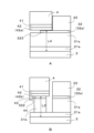
- the height L3 of the second exposed portion 322 and the height L4 of the third exposed portion 323 are the same.
- the height L3 of the second exposed portion 322 can be defined as the distance from the upper surface of the wiring board 2 to the upper surface of the second exposed portion 322 in the thickness direction of the optical circuit board 1 as shown in FIG. 9B, for example. can.
- the height L4 of the third exposed portion 323 can be defined as the distance from the upper surface of the wiring board 2 to the upper surface of the third exposed portion 323 in the thickness direction of the optical circuit board 1 as shown in FIG. 9A, for example. can.
- the height L3 of the second exposed portion 322 and the height L4 of the third exposed portion 323 are the same, not only when they are perfectly matched, but also in consideration of manufacturing errors and the like, for example, (height L3 of second exposed portion 322/height L4 of third portion 323) ⁇ 100 includes a range of 90% to 110%.
- FIGS. 9A and 9B are enlarged explanatory views for explaining cross sections of regions Z3 and Z4 shown in FIG. 8 when the optical component 4 is mounted on the optical circuit board 1 according to one embodiment.
- the second core 42 (linear portion 42a) of the optical component 4 and the third exposed portion 323 of the first core 32 can be overlapped to facilitate adiabatic coupling for transmission.
- the optical circuit board on which such an optical component 4 is mounted in the second mounting region R2 has a height L1 from the top surface of the wiring board 2 to the top of the third exposed portion 323, and a height L1 from the top surface of the wiring board 2 to the second exposed portion.
- the height L2 to the top of 322 is the same. This facilitates alignment in the height direction between the end face of the first core 32 and the end face of the second core 42 of the optical component 4 .
- the optical component 4 can be easily mounted horizontally on the wiring board 2. Become.
- the width W1 of the first portion 31a of the first lower clad 31 where the third exposed portion 323 of the first core 32 is located is equal to the width W1 where the covering portion 32a of the first core 32 is located. It may be smaller than the width W2 of the first portion 31 a of the first lower clad 31 .
- the area where the second core 42 of the optical component 4 is located is narrow, it becomes easy to overlap the optical component 4 and the third exposed portion 323 .
- an electric signal from the wiring board 2 is propagated through the solder 7 to the light source section included in the optical component 4 (silicon photonics device).
- the light source unit that receives the propagated electrical signal emits light.
- An optical fiber in which the emitted optical signal passes through the second core 42 (linear portion 42a) of the optical component 4 and the first core 32 (coated portion 32a) of the optical waveguide 3 and is connected via the optical connector 5a. 5.
- optical circuit board 2 wiring board 21a conductor layer 21b pad 3 optical waveguide 31 first lower clad 31a first portion 31b second portion 32 first core 32a covering portion 321 first exposed portion 322 second exposed portion 323 third exposed portion 33 first upper clad 4 optical component 41 second lower clad 42 second core 42a linear portion 42b planar portion 42c island portion 43 second upper clad 44 concave portion 5 optical fiber 5a optical connector 6 electronic component 7 solder 10 optical component mounting Structure R1 First mounting area R2 Second mounting area
Landscapes
- Physics & Mathematics (AREA)
- General Physics & Mathematics (AREA)
- Optics & Photonics (AREA)
- Engineering & Computer Science (AREA)
- Microelectronics & Electronic Packaging (AREA)
- Optical Integrated Circuits (AREA)
- Optical Couplings Of Light Guides (AREA)
Priority Applications (4)
| Application Number | Priority Date | Filing Date | Title |
|---|---|---|---|
| CN202380022098.8A CN118696257A (zh) | 2022-02-22 | 2023-02-21 | 光电路基板 |
| US18/838,791 US20250155657A1 (en) | 2022-02-22 | 2023-02-21 | Optical circuit board |
| KR1020247027129A KR20240132507A (ko) | 2022-02-22 | 2023-02-21 | 광회로 기판 |
| JP2024503164A JP7744501B2 (ja) | 2022-02-22 | 2023-02-21 | 光回路基板 |
Applications Claiming Priority (2)
| Application Number | Priority Date | Filing Date | Title |
|---|---|---|---|
| JP2022025565 | 2022-02-22 | ||
| JP2022-025565 | 2022-02-22 |
Publications (1)
| Publication Number | Publication Date |
|---|---|
| WO2023162964A1 true WO2023162964A1 (ja) | 2023-08-31 |
Family
ID=87765928
Family Applications (1)
| Application Number | Title | Priority Date | Filing Date |
|---|---|---|---|
| PCT/JP2023/006186 Ceased WO2023162964A1 (ja) | 2022-02-22 | 2023-02-21 | 光回路基板 |
Country Status (6)
| Country | Link |
|---|---|
| US (1) | US20250155657A1 (https=) |
| JP (1) | JP7744501B2 (https=) |
| KR (1) | KR20240132507A (https=) |
| CN (1) | CN118696257A (https=) |
| TW (1) | TWI854503B (https=) |
| WO (1) | WO2023162964A1 (https=) |
Cited By (2)
| Publication number | Priority date | Publication date | Assignee | Title |
|---|---|---|---|---|
| WO2025127057A1 (ja) * | 2023-12-15 | 2025-06-19 | イビデン株式会社 | 配線基板 |
| WO2025197844A1 (ja) * | 2024-03-19 | 2025-09-25 | イビデン株式会社 | 光導波路及び導波路搭載基板 |
Citations (8)
| Publication number | Priority date | Publication date | Assignee | Title |
|---|---|---|---|---|
| US5721797A (en) * | 1996-05-28 | 1998-02-24 | Lucent Technologies Inc. | Apparatus and method for mounting a laser to a substrate and aligning the laser with an optical conduit |
| JP2000347052A (ja) * | 1999-04-02 | 2000-12-15 | Toppan Printing Co Ltd | 光・電気配線基板及びその製造方法並びに実装基板 |
| JP2001091794A (ja) * | 1999-09-20 | 2001-04-06 | Nec Corp | 光モジュールの実装方法及び実装構造 |
| JP2002202425A (ja) * | 2000-12-28 | 2002-07-19 | Nec Corp | 光モジュール及びその製造方法 |
| JP2003517630A (ja) * | 1999-07-16 | 2003-05-27 | ハイブリッド マイクロ テクノロジーズ アンパーツゼルスカブ | Si基板上の能動光学素子および受動光学素子のハイブリッド集積 |
| KR20050070263A (ko) * | 2003-12-30 | 2005-07-07 | 마이크로솔루션스 주식회사 | 복합형 광소자, 복합형 광소자용 실리콘 광학 벤치,복합형 광소자용 평면형 광도파로 소자, 복합형 광소자의제조방법, 및 이를 위한 광소자의 광축 정렬 방법 |
| JP2005266179A (ja) * | 2004-03-17 | 2005-09-29 | Omron Corp | 光導波路装置及び光導波路装置の製造方法並びに光導波路装置の中間体 |
| JP2021026022A (ja) * | 2019-07-31 | 2021-02-22 | 京セラ株式会社 | 光導波路モジュール及び光源モジュール |
Family Cites Families (2)
| Publication number | Priority date | Publication date | Assignee | Title |
|---|---|---|---|---|
| JPS6264832U (https=) | 1985-10-09 | 1987-04-22 | ||
| CN103066148B (zh) * | 2012-12-28 | 2015-05-20 | 武汉电信器件有限公司 | 一种硅上二氧化硅基的混合集成光电子芯片及其制作方法 |
-
2023
- 2023-02-21 US US18/838,791 patent/US20250155657A1/en active Pending
- 2023-02-21 KR KR1020247027129A patent/KR20240132507A/ko not_active Withdrawn
- 2023-02-21 JP JP2024503164A patent/JP7744501B2/ja active Active
- 2023-02-21 CN CN202380022098.8A patent/CN118696257A/zh active Pending
- 2023-02-21 WO PCT/JP2023/006186 patent/WO2023162964A1/ja not_active Ceased
- 2023-02-22 TW TW112106510A patent/TWI854503B/zh active
Patent Citations (8)
| Publication number | Priority date | Publication date | Assignee | Title |
|---|---|---|---|---|
| US5721797A (en) * | 1996-05-28 | 1998-02-24 | Lucent Technologies Inc. | Apparatus and method for mounting a laser to a substrate and aligning the laser with an optical conduit |
| JP2000347052A (ja) * | 1999-04-02 | 2000-12-15 | Toppan Printing Co Ltd | 光・電気配線基板及びその製造方法並びに実装基板 |
| JP2003517630A (ja) * | 1999-07-16 | 2003-05-27 | ハイブリッド マイクロ テクノロジーズ アンパーツゼルスカブ | Si基板上の能動光学素子および受動光学素子のハイブリッド集積 |
| JP2001091794A (ja) * | 1999-09-20 | 2001-04-06 | Nec Corp | 光モジュールの実装方法及び実装構造 |
| JP2002202425A (ja) * | 2000-12-28 | 2002-07-19 | Nec Corp | 光モジュール及びその製造方法 |
| KR20050070263A (ko) * | 2003-12-30 | 2005-07-07 | 마이크로솔루션스 주식회사 | 복합형 광소자, 복합형 광소자용 실리콘 광학 벤치,복합형 광소자용 평면형 광도파로 소자, 복합형 광소자의제조방법, 및 이를 위한 광소자의 광축 정렬 방법 |
| JP2005266179A (ja) * | 2004-03-17 | 2005-09-29 | Omron Corp | 光導波路装置及び光導波路装置の製造方法並びに光導波路装置の中間体 |
| JP2021026022A (ja) * | 2019-07-31 | 2021-02-22 | 京セラ株式会社 | 光導波路モジュール及び光源モジュール |
Cited By (2)
| Publication number | Priority date | Publication date | Assignee | Title |
|---|---|---|---|---|
| WO2025127057A1 (ja) * | 2023-12-15 | 2025-06-19 | イビデン株式会社 | 配線基板 |
| WO2025197844A1 (ja) * | 2024-03-19 | 2025-09-25 | イビデン株式会社 | 光導波路及び導波路搭載基板 |
Also Published As
| Publication number | Publication date |
|---|---|
| CN118696257A (zh) | 2024-09-24 |
| TW202343048A (zh) | 2023-11-01 |
| JP7744501B2 (ja) | 2025-09-25 |
| JPWO2023162964A1 (https=) | 2023-08-31 |
| KR20240132507A (ko) | 2024-09-03 |
| TWI854503B (zh) | 2024-09-01 |
| US20250155657A1 (en) | 2025-05-15 |
Similar Documents
| Publication | Publication Date | Title |
|---|---|---|
| JP7617248B2 (ja) | 光回路基板およびそれを用いた光学部品実装構造体 | |
| JP7744501B2 (ja) | 光回路基板 | |
| CN114127601B (zh) | 光电路基板以及使用了该光电路基板的电子部件安装构造体 | |
| US12481109B2 (en) | Optical circuit board and electronic component mounting structure using the same | |
| JP7818626B2 (ja) | 光回路基板および光学部品実装構造体 | |
| JP7813873B2 (ja) | 光回路基板 | |
| JP7710784B2 (ja) | 光回路基板および光学部品実装構造体 | |
| TWI917915B (zh) | 光迴路基板及安裝構造體 | |
| JP7788203B2 (ja) | 光回路基板およびそれを用いた光学部品実装構造体 | |
| WO2023095768A1 (ja) | 光回路基板 | |
| WO2025206001A1 (ja) | 光回路基板および実装構造体 | |
| WO2025183093A1 (ja) | 光回路基板および実装構造体 | |
| US20250199237A1 (en) | Optical waveguide device and substrate with optical waveguides | |
| WO2024204111A1 (ja) | 光回路基板および実装構造体 |
Legal Events
| Date | Code | Title | Description |
|---|---|---|---|
| 121 | Ep: the epo has been informed by wipo that ep was designated in this application |
Ref document number: 23759965 Country of ref document: EP Kind code of ref document: A1 |
|
| ENP | Entry into the national phase |
Ref document number: 2024503164 Country of ref document: JP Kind code of ref document: A |
|
| ENP | Entry into the national phase |
Ref document number: 20247027129 Country of ref document: KR Kind code of ref document: A |
|
| WWE | Wipo information: entry into national phase |
Ref document number: 18838791 Country of ref document: US Ref document number: 202380022098.8 Country of ref document: CN |
|
| NENP | Non-entry into the national phase |
Ref country code: DE |
|
| 122 | Ep: pct application non-entry in european phase |
Ref document number: 23759965 Country of ref document: EP Kind code of ref document: A1 |
|
| WWP | Wipo information: published in national office |
Ref document number: 18838791 Country of ref document: US |