WO2023157624A1 - Interposer, semiconductor package, and methods for manufacturing same - Google Patents
Interposer, semiconductor package, and methods for manufacturing same Download PDFInfo
- Publication number
- WO2023157624A1 WO2023157624A1 PCT/JP2023/002842 JP2023002842W WO2023157624A1 WO 2023157624 A1 WO2023157624 A1 WO 2023157624A1 JP 2023002842 W JP2023002842 W JP 2023002842W WO 2023157624 A1 WO2023157624 A1 WO 2023157624A1
- Authority
- WO
- WIPO (PCT)
- Prior art keywords
- interposer
- layer structure
- outer layer
- insulating resin
- semiconductor package
- Prior art date
Links
Images


Classifications
-
- H—ELECTRICITY
- H01—ELECTRIC ELEMENTS
- H01L—SEMICONDUCTOR DEVICES NOT COVERED BY CLASS H10
- H01L23/00—Details of semiconductor or other solid state devices
- H01L23/12—Mountings, e.g. non-detachable insulating substrates
-
- H—ELECTRICITY
- H01—ELECTRIC ELEMENTS
- H01L—SEMICONDUCTOR DEVICES NOT COVERED BY CLASS H10
- H01L23/00—Details of semiconductor or other solid state devices
- H01L23/12—Mountings, e.g. non-detachable insulating substrates
- H01L23/14—Mountings, e.g. non-detachable insulating substrates characterised by the material or its electrical properties
-
- H—ELECTRICITY
- H01—ELECTRIC ELEMENTS
- H01L—SEMICONDUCTOR DEVICES NOT COVERED BY CLASS H10
- H01L23/00—Details of semiconductor or other solid state devices
- H01L23/32—Holders for supporting the complete device in operation, i.e. detachable fixtures
-
- H—ELECTRICITY
- H01—ELECTRIC ELEMENTS
- H01L—SEMICONDUCTOR DEVICES NOT COVERED BY CLASS H10
- H01L25/00—Assemblies consisting of a plurality of individual semiconductor or other solid state devices ; Multistep manufacturing processes thereof
- H01L25/03—Assemblies consisting of a plurality of individual semiconductor or other solid state devices ; Multistep manufacturing processes thereof all the devices being of a type provided for in the same subgroup of groups H01L27/00 - H01L33/00, or in a single subclass of H10K, H10N, e.g. assemblies of rectifier diodes
- H01L25/04—Assemblies consisting of a plurality of individual semiconductor or other solid state devices ; Multistep manufacturing processes thereof all the devices being of a type provided for in the same subgroup of groups H01L27/00 - H01L33/00, or in a single subclass of H10K, H10N, e.g. assemblies of rectifier diodes the devices not having separate containers
- H01L25/065—Assemblies consisting of a plurality of individual semiconductor or other solid state devices ; Multistep manufacturing processes thereof all the devices being of a type provided for in the same subgroup of groups H01L27/00 - H01L33/00, or in a single subclass of H10K, H10N, e.g. assemblies of rectifier diodes the devices not having separate containers the devices being of a type provided for in group H01L27/00
-
- H—ELECTRICITY
- H01—ELECTRIC ELEMENTS
- H01L—SEMICONDUCTOR DEVICES NOT COVERED BY CLASS H10
- H01L25/00—Assemblies consisting of a plurality of individual semiconductor or other solid state devices ; Multistep manufacturing processes thereof
- H01L25/03—Assemblies consisting of a plurality of individual semiconductor or other solid state devices ; Multistep manufacturing processes thereof all the devices being of a type provided for in the same subgroup of groups H01L27/00 - H01L33/00, or in a single subclass of H10K, H10N, e.g. assemblies of rectifier diodes
- H01L25/04—Assemblies consisting of a plurality of individual semiconductor or other solid state devices ; Multistep manufacturing processes thereof all the devices being of a type provided for in the same subgroup of groups H01L27/00 - H01L33/00, or in a single subclass of H10K, H10N, e.g. assemblies of rectifier diodes the devices not having separate containers
- H01L25/07—Assemblies consisting of a plurality of individual semiconductor or other solid state devices ; Multistep manufacturing processes thereof all the devices being of a type provided for in the same subgroup of groups H01L27/00 - H01L33/00, or in a single subclass of H10K, H10N, e.g. assemblies of rectifier diodes the devices not having separate containers the devices being of a type provided for in group H01L29/00
-
- H—ELECTRICITY
- H01—ELECTRIC ELEMENTS
- H01L—SEMICONDUCTOR DEVICES NOT COVERED BY CLASS H10
- H01L25/00—Assemblies consisting of a plurality of individual semiconductor or other solid state devices ; Multistep manufacturing processes thereof
- H01L25/18—Assemblies consisting of a plurality of individual semiconductor or other solid state devices ; Multistep manufacturing processes thereof the devices being of types provided for in two or more different subgroups of the same main group of groups H01L27/00 - H01L33/00, or in a single subclass of H10K, H10N
-
- H—ELECTRICITY
- H05—ELECTRIC TECHNIQUES NOT OTHERWISE PROVIDED FOR
- H05K—PRINTED CIRCUITS; CASINGS OR CONSTRUCTIONAL DETAILS OF ELECTRIC APPARATUS; MANUFACTURE OF ASSEMBLAGES OF ELECTRICAL COMPONENTS
- H05K3/00—Apparatus or processes for manufacturing printed circuits
- H05K3/46—Manufacturing multilayer circuits
Definitions
- the present invention relates to an interposer for mounting a semiconductor device, a semiconductor package in which the semiconductor device is mounted on the interposer, and a method of manufacturing them.
- SiP System In Package
- HBM High Bandwidth Memory
- the HBM generally has a narrow pitch of about 55 ⁇ m between the connection terminals, and it is necessary to form the same degree of connection terminals on the interposer.
- the interposer as described above is connected to the FC-BGA, and the CTE (Coefficient of Thermal Expansion) of the FC-BGA is about 18 ppm/°C, which is higher than the CTE of the semiconductor chip, which is 3 ppm/°C. . Therefore, the interposer is required to have a function of alleviating the CTE mismatch between the semiconductor chip and the FC-BGA. Furthermore, for the convenience of assembly as a semiconductor package, it is desirable to be able to mount the semiconductor device on the interposer and then mount it on the FC-BGA. For this reason, the interposer must be able to exist as an independent unit separate from the FC-BGA.
- Patent Document 1 in order to suppress warpage of the interposer, as a method of manufacturing a semiconductor package (1), a plate-like first reinforcing member (5A) and a first conductor pattern wiring board laminate (2A) are used. and a plate-shaped second reinforcing member (4A) disposed on a second conductor pattern (224); and heating the laminate (20) to remove the insulating layer.
- a step of thermally curing a step of selectively removing a portion of the first reinforcing member (5A) to form an opening for exposing the first conductor pattern (224); ) to form an opening 41 for exposing the second conductor pattern (221) and the second conductor pattern (221) exposed from the opening of the second reinforcing member (4A) ) and connecting the semiconductor element (3).
- the interposer shown in Patent Document 1 has a structure in which a fiber base material is impregnated with a resin composition, the diameter of vias that can be formed is limited to a diameter of 50 ⁇ m. Also, the pitch between vias is limited to 130 ⁇ m, making it difficult to mount an HBM, which is a stacked DRAM.
- interposers such as fan-out packages and silicon interposers, and semiconductor packages using these interposers, are not supposed to go through a step of mounting a semiconductor device after inspecting the interposer itself. For this reason, in the conventional manufacturing method, a plurality of chips are mounted on the interposer under the condition that the interposer itself is not guaranteed to be inspected. As a result, the yield of semiconductor packages is the sum of interposer manufacturing defects and chip mounting defects, and cannot be separated from each other.
- the SiP manufacturing yield can be simply described by the following trial calculation formula (1).
- "Interposer Yield” (Y INTERPOSER ): (value between 0 and 1)
- Geometric mean yield of semiconductor chip mounting (mounting yield” (Y ASSEMBRY ): (value between 0 and 1)
- SiP manufacturing yield (Y TOTAL ): (value between 0 and 1)
- the manufacturing yield of SiP is as follows.
- (Y TOTAL ) (Y INTERPOSER ) x (Y ASSEMBRY ) N (1)
- the SiP manufacturing yield is the power of the interposer yield and the geometric mean yield of chip mounting multiplied by the number of chips.
- the overall manufacturing yield of SiP is extremely low.
- an object of the present invention is to provide an interposer capable of forming terminals for connection of a semiconductor device with a narrow pitch of 60 ⁇ m or less, and allowing electrical inspection of the interposer itself before mounting the semiconductor device.
- one representative interposer of the present invention is an inner layer structure including at least one inner layer wiring layer; a first outer layer structure disposed on the first main surface of the inner layer structure and having higher rigidity than the inner layer structure;
- the inner wiring layer includes wiring arranged on the surface of the first insulating resin layer and a conductive member connected to the wiring and penetrating the first insulating resin layer,
- the first outer layer structure and the second outer layer structure each include a second insulating resin layer and a conductive member penetrating through the second insulating resin,
- the first outer layer structure and/or the second outer layer structure is a terminal that can be connected to a semiconductor device and that can be electrically tested on a surface opposite to the surface that is connected to the inner layer structure. It has
- an interposer capable of forming connection terminals of a semiconductor device with a narrow pitch of 60 ⁇ m or less and being electrically inspectable before mounting the semiconductor device.
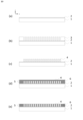
- FIG. 1 is a cross-sectional view of the interposer and semiconductor package of the first embodiment.
- FIG. 2 is a diagram showing the relationship between the overall CTE and the CTE of the outer wiring layer.
- FIG. 3 is a diagram showing the relationship between the manufacturing defect rate and the thickness.
- FIG. 4 is a schematic diagram showing a modification of the interposer of the first embodiment.
- FIG. 5 is a schematic diagram showing a modification of the interposer of the first embodiment.
- FIG. 6 is a schematic diagram showing a modification of the interposer of the first embodiment.
- 7A and 7B are diagrams for explaining a manufacturing process of the interposer and the semiconductor package according to the first embodiment.
- 8A and 8B are diagrams for explaining the steps of manufacturing the interposer and the semiconductor package of the first embodiment.
- FIGS. 9A and 9B are diagrams for explaining the steps of manufacturing the interposer and the semiconductor package according to the first embodiment.
- 10A and 10B are diagrams for explaining the steps of manufacturing the interposer and the semiconductor package of the first embodiment.
- 11A and 11B are diagrams for explaining the manufacturing process of the interposer of the modification of the first embodiment.
- 12A and 12B are diagrams for explaining the manufacturing process of the semiconductor package of the first embodiment.
- 13A and 13B are diagrams for explaining the manufacturing process of the semiconductor package of the first embodiment.
- FIG. 14 is a schematic diagram showing the interposer of the second embodiment.
- 15A and 15B are diagrams illustrating a method for manufacturing an interposer according to the second embodiment.
- FIG. 16 is a schematic diagram showing the interposer and semiconductor package of the third embodiment.
- FIG. 17A and 17B are diagrams illustrating a method for manufacturing an interposer according to the third embodiment.
- 18A and 18B are diagrams illustrating a method for manufacturing an interposer according to the third embodiment.
- FIG. 19 is a schematic diagram showing the interposer and semiconductor package of the fourth embodiment.
- 20A and 20B are diagrams illustrating a method for manufacturing an interposer and a semiconductor package according to the fourth embodiment.
- 21A and 21B are diagrams for explaining a method for manufacturing a semiconductor package according to the fourth embodiment.
- FIG. 22 is a diagram explaining an outline of a four-point bending test.
- FIG. 23 is a table showing standard values of deflection speed in a four-point bending test.
- FIG. 24 is a diagram showing the relationship between the thickness of the interposer and the ratio of the load and the amount of deflection in the four-point bending test.
- FIG. 25 is a schematic diagram showing the interposer and semiconductor package of the fifth embodiment.
- 26A and 26B are diagrams illustrating a method for manufacturing an interposer and a semiconductor package according to the fifth embodiment.
- 27A and 27B are diagrams illustrating a method for manufacturing an interposer and a semiconductor package according to Modification 1 of the fifth embodiment.
- 28A and 28B are diagrams for explaining a method for manufacturing an interposer and a semiconductor package according to Modification 2 of the fifth embodiment.
- the term “surface” may refer not only to the surface of the plate-like member, but also to the interface between the layers included in the plate-like member that is substantially parallel to the surface of the plate-like member.
- the terms “upper surface” and “lower surface” refer to the upper or lower surface of the drawing when a plate-like member or a layer included in the plate-like member is illustrated.
- the “upper surface” and “lower surface” may also be referred to as “first surface” and "second surface”.
- the “side surface” means a surface of a plate-like member or a layer included in the plate-like member or a portion of the thickness of the layer. Furthermore, a part of a surface and a side surface may be collectively referred to as an "end”. Moreover, “upper” means the vertically upward direction when the plate-like member or layer is placed horizontally. Further, “upward” and “downward” opposite to this are sometimes referred to as “Z-axis positive direction” and “Z-axis negative direction”, and horizontal directions are referred to as “X-axis direction” and "Y-axis direction”. It is sometimes called “direction”.
- planar shape and planar view mean the shape when a surface or layer is viewed from above.
- cross-sectional shape and cross-sectional view mean the shape of a plate-like member or layer cut in a specific direction and viewed from the horizontal direction.
- core means the core of a face or layer, but not the periphery.
- central direction means a direction from the periphery of a surface or layer toward the center of the planar shape of the surface or layer.
- FIG. 1(a) is an example of a schematic cross-sectional view of an interposer 100 according to a first embodiment of the present invention.
- FIG. 1B is a schematic sectional view of a semiconductor package 150 in which semiconductor devices 50 and 51 are mounted on the interposer 100 of the first embodiment.
- the first surface side the side on which the semiconductor devices 50 and 51 are mounted
- the side where the interposer 100 is connected to the motherboard or FC-BGA is referred to as the "first surface side.” 2 sides”.
- the second connection terminals 17 are arranged on the second surface side of the second outer layer structure 11 .
- the second connection terminal 17 serves as a connection terminal to the FC-BGA board or motherboard.
- the interposer 100 in FIG. 1( a ) is mainly composed of a first outer layer structure 5 , an inner layer structure 7 and a second outer layer structure 11 .
- the first outer layer structure 5 is arranged above the inner layer structure 7, that is, in the positive Z-axis direction.
- the first outer layer structure 5 is formed of a second insulating resin layer 6, and the second insulating resin layer 6 is formed with a conductive member 4 penetrating through the second insulating resin layer 6 in the Z-axis direction. there is
- the conductive member 4 penetrating the second insulating resin layer 6 can function as a pad for the external connection terminal of the first outer layer structure 5 .
- a first connection terminal 16 is arranged on the first surface side of the first outer layer structure 5 .
- the inner layer structure 7 is arranged between the first outer layer structure 5 and the second outer layer structure 11 .
- the inner layer structure 7 has at least one inner layer wiring layer, and the inner layer wiring layer includes a first insulating resin layer 8, a wiring 10 disposed on the surface of the first insulating resin layer, and a wiring 10 for the wiring 10.
- a conductive member is provided that connects and penetrates the first insulating resin layer in the Z-axis direction. Also, the conductive member penetrating the first insulating resin layer can function as the via 9 of the inner wiring layer.
- a first connection terminal (solder) 16 is arranged on the first surface side of the first outer layer structure 5 .
- the second outer layer structure 11 is arranged below the inner layer structure 7, that is, in the negative Z-axis direction.
- the second outer layer structure 11 is formed of a second insulating resin layer 12, and a conductive member is formed in the second insulating resin layer 12 so as to penetrate the second insulating resin layer 12 in the Z-axis direction.
- the conductive member penetrating the second insulating resin layer 12 is connected to the outermost wiring layer of the inner layer structure 7 and can function as a pad for the external connection terminal of the second outer layer structure 11 .
- pads 15 of external connection terminals and second connection terminals (solder) 17 are arranged on the second surface side of the second outer layer structure 11 .
- the total thickness including the inner layer structure 7, the first outer layer structure 5 and the second outer layer structure 11 is preferably 50 ⁇ m or more.
- the thicknesses of the first outer layer structure 5 and the second outer layer structure 11 of the interposer 100 in the present embodiment are not limited to the thicknesses employed in the present embodiment.
- the second outer layer structure 11 has higher physical rigidity than the inner layer structure 7, the sum of the thicknesses of the first outer layer structure 5 and the second outer layer structure 11 is thicker than the inner layer structure 7. is desirable. That is, it is desirable that the thickness of the first outer layer structure 5 and the second outer layer structure 11 be more than half of the total thickness of the interposer 100 .
- FIG. 1B shows a semiconductor package 150 in which semiconductor devices 50 and 51 are fixed to the first surface side of the interposer 100 explained in FIG.
- first connection terminal 16 and the second connection terminal 17 are made of solder, the solder type and solder composition are not limited by the present invention, and known conductive materials can be used. 1(a) and 1(b), the first connection terminal 16 is formed flush with the conductive member 4 of the first outer layer structure 5. The positional relationship and shape of the member 4 are not limited to this. Similarly, the second connection terminals 17 are formed in alignment with the external terminal pads 15 on the vias 14 of the second external layer structure 11, but are not necessarily limited to such a structure.
- the inner layer structure 7 forms a fine wiring structure required for a SiP interposer on which a plurality of semiconductor devices are mounted.
- the input/output terminal portion of the inner layer structure 7 is formed by the first outer layer structure 5 and the second outer layer structure 11 for physical rigidity. Since the input/output terminal portion has a margin in the wiring rule compared to the fine wiring in the inner layer structure 7, the first outer layer structure 5 and the second outer layer structure 11 are formed using a rigid material. becomes possible. Therefore, by sandwiching the inner layer structure 7 having no physical rigidity between the first outer layer structure 5 and the second outer layer structure 11 having physical rigidity, the interposer 100 as a whole is configured as a device having rigidity. becomes possible. In other words, by dividing the functions of the circuit fine characteristics and the physical rigidity characteristics into the inner layer structure 7 and the two outer layer structures and combining the contradictory characteristics, an interposer that combines the excellent characteristics of both is realized. It is.
- the second insulating resin layer forming the first outer layer structure 5 and the second outer layer structure 11 is preferably selected from non-photosensitive insulating resins containing fillers.
- the second insulating resin layer is a non-photosensitive resin layer containing a filler, and may be selected from prepregs, built-up resins, and molded resins having an elastic modulus of 5 GPa or more and a linear thermal expansion coefficient CTE of 20 ppm or less. More preferred.
- the first insulating resin layer that can be applied to the inner layer structure 7 in the present embodiment is a photosensitive insulating resin or a built-up resin, and has general material properties such as a CTE of 20 ppm to 80 ppm/° C. and an elastic modulus of 1.5. It is a low modulus and high CTE material ranging from to 10 GPa or less. Therefore, if the interposer is formed only from the above materials, the CTE is lower than the CTE of FC-BGA, 18 ppm/° C., and it is difficult to realize an interposer that functions as a buffer against the low CTE of the semiconductor device.
- the second insulating resin layer used for the first outer layer structure 5 and the second outer layer structure 11 has a CTE of 20 ppm/° C. or less and a high elastic modulus of 5 GPa or more.
- FIG. 2 shows simulation results of the relationship between the CTE of the entire interposer with a total thickness of 50 ⁇ m and the CTE and elastic modulus of the materials used for the first outer layer structure and the second outer layer structure in the present invention.
- the CTE of the entire interposer is plotted on the Y-axis, and the CTE of the X first and second outer wiring layers are plotted. Simulation conditions are as follows. The CTE and elastic modulus of the first outer wiring layer and the second outer wiring layer were calculated as the same factor.
- the results of the simulation under these conditions are shown in the graph of FIG. That is, as is clear from FIG. 2, by using the CTE of the first outer layer structure 5 and the second outer layer structure 11 of 20 ppm/° C. or less, the CTE of the entire interposer 100 is reduced to that of the FC-BGA of the prior art. It can be seen that it can be made lower than the substrate. It can also be seen that the more highly elastic materials are used for the first outer layer structure 5 and the second outer layer structure 11, the greater the effect of reducing the CTE of the entire interposer. From these facts, it was found that the CTE of the entire interposer can be effectively reduced if the elastic moduli of the first outer layer structure 5 and the second outer layer structure 11 are 5 GPa or more. It is desirable to select from 5 GPa or more.
- the conductive members 4, vias 14, and pads 15 of the first outer layer structure 5 and the second outer layer structure 11 of the interposer 100 of the embodiment shown in FIG. and the wiring of the inner layer structure 7 are electrically connected. Therefore, the first outer layer structure 5 and the second outer layer structure 11 are basically formed with connection paths in the Z direction.
- wiring suitable for miniaturization is used to realize wiring routing in the Z-axis direction and in the direction perpendicular to the Z-axis, that is, in the horizontal direction. Copper is basically used as the conductive member used in the interposer in this embodiment.
- a high ratio makes it difficult to achieve a low CTE for the entire interposer 100 . Therefore, it is desirable that the residual copper ratio in the first outer layer structure 5 and the second outer layer structure 11 is 80% or less. More desirably, it is 50% or less. More desirably, it is 30% or less.
- FIG. 22 is a diagram explaining an outline of a four-point bending test.
- FIG. 23 is a table showing the standard values of the test speed of the four-point bending test. The rigidity of the interposer 100 is evaluated based on the load and deflection amount when a test piece 101 obtained by processing the interposer 100 is subjected to a bending test.
- the bending test includes a 3-point bending test and a 4-point bending test, and the 4-point bending test is adopted in this embodiment.
- the bending force applied to the test piece is not uniform, and the test piece 101 bends and stretches on the inside and outside of the bend. For this reason, in a multi-layered structure such as the interposer 100, different results may be obtained depending on the arrangement of each material in the thickness direction.
- the bending force applied to the test piece 101 is uniform, enabling highly accurate measurement.
- test conditions for the four-point bending test for evaluating the interposer 100 are as follows. ⁇ Dimensions of test piece 101: length 80 mm x width 15 mm x height h (thickness of interposer 100) mm ⁇ Distance L between fulcrums: 66 mm ⁇ Indenter radius r1: 2 mm ⁇ Distance between indenters L′: 22 mm ⁇ Support radius r2: 2 mm ⁇ Deflection speed V: Calculated by the following formula 1
- the interposer 100 does not have a shape with specific dimensions for use as a test piece, first, the interposer 100 is processed to have a specific size (length 80 mm ⁇ width 15 mm ⁇ height h mm) as a test piece.
- the interposer 100 may be used as the test piece 101 as it is if it has specific dimensions specified by the test conditions.
- the test equipment used in the four-point bending test satisfies the distance L between the fulcrums, the radius r1 of the indenter, the distance L′ between the indenters, the radius of the support r2, and the test speed specified in FIG. do.
- the test apparatus used in the 4-point bending test comprises two cylindrical supports 61 and two cylindrical indenters 60 that meet ISO 5893.
- the test speed V is calculated from Equation (5).
- a strain rate of 0.01 [1/min] (1%/min) is selected.
- a load of F/2 is applied to each of the indenters 60 in order to apply a load F to the vertical and horizontal surfaces of the test piece 101 .
- the load F is a load such that the deflection speed of the test piece 101 becomes the test speed V.
- FIG. From the load F and the amount of deflection obtained by the four-point bending test, the ratio of the amount of load F to the amount of deflection is calculated.
- the rigidity of the interposer can be evaluated from the ratio between the load F of the indenter and the amount of deflection obtained at this time.
- the inner layer structure 7 having a fine wiring structure is formed by forming the first outer layer structure 5 and the second outer layer structure 11 over both surfaces of the inner layer structure 7. Reliability can be improved. If the first outer layer structure 5 and the second outer layer structure 11 are only partially formed on the upper and lower surfaces of the inner layer structure 7, cracks may occur in the inner layer structure 7 due to deformation and stress concentration. It turns out.
- the first outer layer structure 5 and the second outer layer structure 11 need to be formed on the entire surfaces of both surfaces of the inner layer structure 7 .
- physical properties and specific materials used for the first outer layer structure 5 and the second outer layer structure 11 are not specified in this embodiment, the CTE of the first outer layer structure 5 and the second outer layer structure 11 is Close is preferred.
- the probe load is 0.05 N and the maximum deflection amount of the probe is 0.4 mm. 125 N/mm, and if the test piece exhibits a value of 125 N/mm or more, it can be judged that it has sufficient rigidity.
- the ratio of the load/deflection amount of the indenter in the four-point bending test of the interposer 100 is set to 0.125 N/mm or more, the interposer 100 can be satisfactorily electrically inspected. That is, a needle-like electrode called a probe used for electrical inspection is brought into contact with the electrode exposed in the outermost layer of the interposer 100, and sufficient electrical contact can be obtained between the probe and the electrode.
- the test speed V is 30 mm/sec.
- the load F indicates 5.7 N
- the deflection amount is 7 mm
- the ratio of the load/deflection amount of the indenter is 0.814 N/mm, which satisfies the requirement.
- FIG. 24 is an example of a diagram showing, in a solid line, the relationship between the Y axis: the ratio of the load/deflection amount of the indenter in the four-point bending test of the interposer, and the X axis: the thickness of the interposer.
- 0.125 N/mm which is the threshold value of the load/deflection amount ratio of the probe in the electrical inspection, is also written with a dashed line.
- the inner layer structure 7 shown in FIGS. 1( a ) and 1 ( b ) is composed of a first insulating resin layer 8 , wiring 10 , and inner wiring layer vias 9 penetrating the first insulating resin layer 8 .
- the thickness, the number of layers, the wiring layer pattern, the shape of vias, the taper direction of vias, the number of vias, and the like of the constituent elements of the inner wiring layer in this embodiment are not limited by this embodiment.
- the inner layer structure 7 may have a single inner wiring layer or a plurality of inner wiring layers, and the number of layers and thickness are not limited by the present embodiment. When assuming application to SiP, it is preferable that the inner wiring layer is formed in a plurality of layers.
- the second insulating resin layer 12 which is a component of the first outer layer structure 5 and the second outer layer structure 11 in FIG. It can be selected from resins, epoxy-cyanate resins, cyanate resins, benzocyclobutenes, polyimides, polybenzoxazoles, and the like. Further, it may contain filler or glass cloth.
- the first insulating resin layer 8 which is a constituent element of the inner layer structure 7 in FIG. etc. can be applied.
- a non-photosensitive insulating resin may be used for the first insulating resin layer 8 .
- the first insulating resin layer 8 can use epoxy-phenol resin, epoxy-phenol ester resin, epoxy-cyanate resin, cyanate resin, benzocyclobutene, polyimide, and polybenzoxazole.
- the first insulating resin layer 8 may further contain filler or glass cloth. Thereby, the first insulating resin layer 8 can impart high rigidity to the interposer.
- first insulating resin layer 8 is a photosensitive insulating resin
- minute vias with a diameter of 20 ⁇ m or less can be formed with a photolithographic positional accuracy of ⁇ 3 ⁇ m or less. Therefore, it is possible to maximize the number of semiconductor devices mounted on the interposer and maximize the number of connection vias.
- it is a photosensitive insulating resin, it is advantageous in that the via formation time does not depend on the number of vias and can be formed all at once.
- vias are formed by laser processing or the like, but the positional accuracy is about ⁇ 10 ⁇ m, and processing time increases as the number of vias increases.
- the thickness of the first insulating resin layer 8 is 25 ⁇ m or less.
- the thickness of the first insulating resin layer 8 referred to here refers to the resin thickness between upper and lower copper wiring patterns.
- the thickness of the first insulating resin layer is 25 ⁇ m or more, it becomes difficult to form small vias having a diameter of 20 ⁇ m or less, and it becomes difficult to increase the wiring density.
- the thickness of the first insulating resin layer is 15 ⁇ m or less. More preferably, it is 10 ⁇ m or less.
- the thickness of the first insulating resin layer 8 can be appropriately adjusted according to the wiring rule to be applied and the impedance matching of the circuit.
- the diameter of the via 9 in the inner wiring layer is 40 ⁇ m or less.
- the diameter of the via 9 referred to here refers to the maximum diameter portion. If the diameter of the via 9 is 40 ⁇ m or more, it will hinder the high wiring density. More preferably, the diameter is 30 ⁇ m or less. More preferably, the thickness is 20 ⁇ m or less because it can contribute to increasing the wiring density.
- the material used for the wiring 10 may contain single metals such as copper, aluminum, nickel, silver, gold, tungsten, iron, niobium, tantalum, titanium, and chromium, their alloys, or additive elements. A layered structure of these various materials may also be used. Alternatively, conductive paste containing these materials, carbon, conductive resin, or the like may be used. For example, when forming a metal layer on the first insulating resin layer 8 by sputtering, it is common practice to form titanium, chromium, nickel, etc. as a single layer or an alloy layer, and then form copper. It is also preferable to form a layer by electroless copper plating or electroless nickel plating on the upper surface of the first insulating resin layer 8 . Electrolytic copper plating is generally used for the wiring 10 because it is convenient and inexpensive.
- FIG. 4 shows a modification in which the first connection terminal 16 and the second connection terminal 17 are partitioned by the solder resist 21 .
- the connection terminals may be partitioned with a solder resist.
- FIG. 5 is a modified example in which the first outer layer structure 5 is formed of multiple layers.
- the first outer layer structure 5 may be formed of a single layer or may be formed of multiple layers. Whether it is a single layer or multiple layers can be adjusted according to the rigidity required for the interposer. When the first outer layer structure 5 is composed of multiple layers, the thickness of the interposer is greater than 50 ⁇ m, which further increases the rigidity, which is preferable.
- FIG. 6 shows a modification in which the second outer layer structure 11 is formed of multiple layers.
- the second outer layer structure 11 may be formed of a single layer or may be formed of multiple layers. Whether it is a single layer or multiple layers can be adjusted according to the rigidity required for the interposer. Further, the modified examples of FIGS. 4 to 6 may be used in combination on the front and back.
- the conductive member 4 of the second insulating resin layer 6 may include wiring or pads. In addition, wiring may be included in addition to the pads 15 of the second insulating resin layer 12 in the second outer layer structure 11, and modifications thereof are also included in the scope of the present invention. Further, the solder connection interface between the first connection terminal 16 and the second connection terminal 17 can be appropriately surface-treated. The type and thickness of the surface treatment are not particularly limited.
- an interposer can be obtained by the following steps. 1) a first step of forming a first outer layer structure on a support substrate; 2) a second step of forming an inner layer structure above the first outer layer structure; 3) a third step of forming a second outer layer structure above the inner layer structure; 4) a fourth step of separating the first outer layer structure and the support substrate; a fifth step of forming connection terminals on the outermost layers of the first outer layer structure and the second outer layer structure;
- the interposer or the semiconductor package can be manufactured by separating from the support substrate. ⁇ Because there is no supporting substrate, it is possible to perform surface treatment, solder bump formation, and protruding electrode formation on the connection terminals exposed on both sides of the substrate. Thus, the first and second connection terminals can be formed on both sides of the interposer.
- a support substrate 1 is prepared.
- the support substrate 1 for example, a substrate obtained by providing a laser peeling layer on a glass substrate and providing a metal layer 2 on the laser peeling layer can be used.
- the metal layer 2 may be formed by electroless plating or sputtering.
- a support substrate may be used in which a carrier copper foil is formed as the metal layer 2 on a CCL (Cupper Clad laminate) substrate via a prepreg.
- the carrier copper foil has a three-layer structure of carrier copper foil-release layer-ultrathin copper foil, and is a copper foil that can be physically and easily separated at the release layer interface.
- the type of support substrate is not limited to those described above, and various known substrates can be used.
- FIG. 7(b) shows a substrate on which a resist pattern 3 is formed by patterning after forming a resist layer on the metal layer 2 .
- the thickness of the resist is appropriately determined in consideration of the height of the pad to be formed.
- the liquid resist was coated with a thickness of 70 ⁇ m, and a pattern was formed so as to form cylindrical pads with a pitch of 55 ⁇ m and a diameter of 25 ⁇ m as pads of the first connection terminals.
- the conductive member 4 is formed by electrolytic copper plating after the step of FIG. 7(b). After that, the resist was removed.
- the columnar conductive member 4 functions as a pad.
- the copper-plated conductive member 4 is formed with an average height of 65 ⁇ m in the Z direction.
- a known copper roughening treatment (CZ treatment) or a silane coupling treatment may be appropriately performed after displacement tin plating.
- FIG. 7(d) is a diagram in which a non-photosensitive insulating resin that becomes the first outer layer structure 5 is formed.
- the second insulating resin layer 6 made of a non-photosensitive resin in the present embodiment is a non-photosensitive resin containing at least a filler, and is selected from prepregs, built-up resins, and mold resins having an elastic modulus of 5 GPa or more and a CTE of 20 ppm or less. It is desirable that In this embodiment, the second insulating resin layer 6 is formed by vacuum lamination using a film-like molding resin having a thickness of 70 ⁇ m.
- the type, thickness, and formation method of the non-photosensitive resin are not limited to those of this embodiment, and appropriate materials and formation methods can be selected.
- FIG. 7(e) is obtained by grinding the second insulating resin layer 6 with a grinder to expose the conductive member 4 that will be the pad of the first outer layer structure 5 .
- the method of exposing the pad is not limited to the method of this embodiment, and may be polishing with a known grinder, buffing, belt polishing, fly-cut method, or CMP.
- the conductive member 4 that serves as a pad is formed in the second insulating resin layer 6 of the first outer layer structure 5 .
- the first outer layer structure 5 was formed with a thickness of 60 ⁇ m.
- the first insulating resin layer 8 of the inner layer structure 7 is formed above the first outer layer structure 5, and the vias 9 are formed.
- the first insulating resin layer 8 is formed with a thickness of 6 ⁇ m using a photosensitive insulating resin, and vias 9 with a diameter of 15 ⁇ m are formed.
- the vias 9 can be formed by laser processing.
- laser processing general laser processing such as CO 2 laser and UV laser can be used.
- desmear treatment may be appropriately performed after laser processing. Thereby, the residue after laser processing can be removed.
- the first insulating resin layer 8 is formed with a thickness of 10 ⁇ m, and the via 9 with a diameter of 15 ⁇ m is formed.
- FIG. 8G shows a structure in which a seed metal layer (not shown) is formed on the first insulating resin layer 8, a resist pattern 3 is formed, and vias 9 and wiring 10 of the inner wiring layer are formed by electroplating.
- a wiring 10 with a thickness of 2.3 ⁇ m (6 ⁇ m+2.3 ⁇ m including vias) was formed using electroplating.
- a non-photosensitive insulating resin is used for the first insulating resin layer 8, in this embodiment, as in FIG. formed.
- a wiring 10 with a thickness of 5 ⁇ m (10 ⁇ m+5 ⁇ m if vias are included) was formed using electroplating.
- FIG. 8(h) shows a diagram in which the seed metal layer is removed after removing the resist pattern 3, and an internal wiring layer composed of the first insulating resin layer 8, the vias 9, and the wiring 10 is formed.
- the wiring forming method and the insulating resin layer forming method are not limited to the method of the present embodiment, and appropriate forming methods can be selected.
- FIG. 8(i) shows an inner layer structure 7 in which four wirings 10 and four first insulating resin layers 8 are laminated by repeating the steps shown in FIGS. 8(f) to (h) three more times. It is.
- the thickness of the first insulating resin layer 8 per layer is 6 ⁇ m
- the thickness of the wiring 10 is 2 ⁇ m
- the thickness of the wiring 10 in the outermost layer is 12 ⁇ m. This is to prevent the wiring from penetrating when making a via hole in the second insulating resin layer 12 of the outer wiring layer with a laser.
- the thickness of the inner layer structure 7 is 36 ⁇ m.
- the steps shown in FIGS. By repeating the process three more times, the wiring 10 and the first insulating resin layer 8 can each obtain a four-layer lamination.
- the thickness of the first insulating resin layer 8 per layer is 10 ⁇ m
- the thickness of the wiring 10 is 5 ⁇ m
- the thickness of the wiring 10 of the outermost layer is 12 ⁇ m as described above.
- the thickness of the inner layer structure 7 is 52 ⁇ m.
- FIG. 8(j) is a diagram for explaining the process of forming the second outer layer structure 11.
- a prepreg and a copper foil with a carrier which will be the second insulating resin layer 12 of the second outer layer structure 11, are formed above the inner layer structure 7 by lamination press.
- a copper foil with a carrier having a thickness of 18 ⁇ m and a thickness of 3 ⁇ m on the thin foil side is used, and a thin copper foil 13 of 3 ⁇ m is arranged on the prepreg side.
- a prepreg having a thickness of 70 ⁇ m was used.
- the steps after FIG. 8J are common to the case of using the photosensitive insulating resin and the non-photosensitive insulating resin for the first insulating resin layer 8 .
- FIG. 9(k) shows the carrier foil removed from the carrier-attached copper foil and vias 14 formed in the second outer layer structure 11 using a CO 2 laser. After that, the laser opening was subjected to desmear treatment, and electroless copper plating was formed in the via portion to a thickness of 0.6 ⁇ m (not shown). In this embodiment, vias with a diameter of 60 ⁇ m are formed at a pitch of 150 ⁇ m.
- the pads 15 are formed by electrolytic copper plating.
- the surface layer portion of the pad 15 was formed from an electrolytic copper plating layer having a thickness of 18 ⁇ m. That is, the pad 15 has a surface layer thickness (not including the via) of 18 ⁇ m, and includes the via portion (via depth of 70 ⁇ m+18 ⁇ m).
- FIG. 9(m) is a view of forming the second outer layer structure 11 by removing the thin copper foil 13 and the electroless copper plating layer by etching after removing the resist pattern 3 .
- pads 15 having a diameter of 75 ⁇ m and a pad thickness of 15 ⁇ m are formed at a pitch of 150 ⁇ m on the second outer layer structure.
- FIG. 9(n) is an upside-down view of FIG. 9(m), showing the step of removing the support substrate 1.
- FIG. 9 After providing a protective sheet on the surface of the second outer layer structure 11 (not shown), the metal layer 2 is removed by etching, and the protective sheet of the second outer layer structure 11 is further removed (not shown), whereby the first An interposer 100 in which the conductive member 4 and the pad 15 are exposed to the outer layer structure 5 can be obtained.
- the first outer layer structure 5 and the second outer layer structure 11 selected from high-elasticity, low-CTE materials are formed on both surfaces of the inner layer structure 7.
- the interposer 100 having a total thickness of 50 ⁇ m or more is formed.
- the interposer formed in this manner has a rigidity that enables it to be transported as a single interposer. Further, since the support is removed from the interposer, both sides of the interposer are exposed, and the first connection terminals 16 and the second connection terminals 17 can be formed on the front and back sides of the interposer. Become.
- FIG. 10(o) shows a step of surface-treating the conductive member 4 (pad) that is the external connection terminal of the first outer layer structure 5 and the pad 15 that is the external connection terminal of the second outer layer structure 11 .
- Appropriate known methods can be adopted for the type and thickness of these surface treatments.
- solder can be formed on both pad layers.
- a known method such as a screen printing method, a ball mounting method, an electroplating method, or filling molten solder after forming a resist pattern can be appropriately employed.
- electroless Ni/Pd/Au was applied to both surfaces as surface treatment, and solder was formed using a front/back ball mounting method. In this way, the interposer 100 of the present embodiment in which the first connection terminals 16 and the second connection terminals 17 are formed on the first outer layer structure 5 and the second outer layer structure 11 can be obtained.
- FIG. 10(p) shows a process of electrically inspecting the interposer 100 by bringing the electrical inspection probes into contact with the first connection terminals 16 and the second connection terminals 17 on both sides of the interposer 100 at the same time.
- a specific electrical inspection and manufacturing procedure using the results are as follows. 1) a first inspection step of electrically inspecting the interposer from the connection terminals; 2) a first judgment step of judging whether the interposer is good or bad based on the result of the first inspection step; 3) a temporary connection step of mounting the semiconductor device on the interposer judged to be "good” in the first judgment step; 4) a second inspection step of electrically inspecting the semiconductor package temporarily connected in the temporary connection step; 5) a second judgment step of judging the quality of the semiconductor package based on the result of the second inspection step; 6) A repair step of repairing and/or replacing the mounting of the semiconductor measures that were determined to be "no" in the second determination step,
- a third inspection step of electrically inspecting the semiconductor package after the repair step a third judgment step of judging the quality of the semiconductor package based on the result of the third inspection step
- the interposer 100 As described above, the interposer 100 according to the present embodiment has a rigidity that enables it to be transported as a single interposer. Therefore, the interposer 100 itself can be electrically inspected before the semiconductor device is mounted, and the quality of the interposer can be determined. Therefore, it is possible to provide only the interposers that are determined to be non-defective products for the subsequent semiconductor package manufacturing process, thereby contributing to the improvement of the SiP assembly yield.
- FIG. 10(q) shows a step of dicing the panel raw fabric in which a plurality of interposers are continuously formed in a grid pattern according to the present embodiment into individual pieces by dicing at the AA portion, and cutting out the individual interposers.
- FIG. 4 is a diagram showing; Thus, the interposer 100 in this embodiment can be manufactured.
- FIG. 11(a) is similar to FIG. 7(a), and shows a state in which the supporting substrate 1 is, for example, a glass substrate on which a laser peeling layer is provided, and a metal layer 2 is provided on the laser peeling layer. .
- the metal layer 2 may be formed by electroless plating or sputtering, or a carrier copper foil may be formed as the metal layer 2 on a CCL (Copper Clad laminate) substrate via a prepreg.
- a second insulating resin layer 6, which will be a first outer layer structure 5, is formed on the support substrate 1.
- FIG. 11(b) a second insulating resin layer 6, which will be a first outer layer structure 5 is formed on the support substrate 1.
- vias for forming pads of the first outer layer structure 5 are formed by laser processing. After forming the via, a desmear treatment or the like may be performed as appropriate. After that, as shown in FIG. 11D, a metal layer (not shown) is formed on the entire surface including the inside of the via, and a resist pattern 3 is formed. After that, electroplating is performed to fill the vias with metal to form the conductive member 4 .
- the first outer layer structure 5 can be obtained by removing the exposed unnecessary metal layer by etching after removing the photoresist.
- the first outer layer structure made of a single layer was explained, but it is also possible to form a first outer layer structure made up of multiple layers as shown in FIG. 5 by the method of this modified example. is.
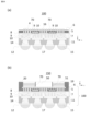
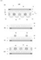
- FIG. 12(a) is a schematic cross-sectional view of a process of mounting semiconductor devices 50 and 51 on an interposer and manufacturing a semiconductor package.
- the interposer used in the present embodiment has undergone an electrical inspection as a single interposer and has been confirmed to be a non-defective product.
- TCB Thermo-Compression bonding
- TCB Thermo-Compression bonding
- NCF Non-Conductive Film
- NCP Non-Conductive Paste
- FIG. 12B is a diagram showing electrical inspection of SiP as a semiconductor package in this embodiment.
- the inspection probe 18 By bringing the inspection probe 18 into contact with the second connection terminal 17 and conducting an electrical inspection, it is possible to inspect the "mounting yield ( YASSEMBRY )" including the individually mounted semiconductor devices, and it is possible to inspect the mounting failure or the semiconductor device. Defects can be identified.
- FIG. 12(c) is a schematic cross-sectional view showing a process of partially removing the semiconductor device 52 having a defective mounting or defect identified in the previous step and replacing it with a non-defective semiconductor device 53.
- FIG. 12(c) is a schematic cross-sectional view showing a process of partially removing the semiconductor device 52 having a defective mounting or defect identified in the previous step and replacing it with a non-defective semiconductor device 53.
- FIG. 12(c) is a schematic cross-sectional view showing a process of partially removing the semiconductor device 52 having a defective mounting or defect identified in the previous step and replacing it with a non-defective semiconductor device 53.
- FIG. 12(c) is a schematic cross-sectional view showing a process of partially removing the semiconductor device 52 having a defective mounting or defect identified in the previous step and replacing it with a non-defective semiconductor device 53.
- FIG. 13(d) is a diagram showing a capillary underfill process for forming the underfill 19 using the underfill supply device 54 on the semiconductor package 150 according to the present embodiment on which a plurality of semiconductor devices are mounted. After inspection and repair, the underfill 19 can be used to fix the semiconductor device to the interposer in this embodiment.
- FIG. 13(e) is a schematic cross-sectional view in which a mold resin 20 is further formed on the semiconductor device. This is not necessarily an essential step in the fixing step using the mold resin. In addition, a known appropriate method can be adopted for fixing with a mold. Furthermore, the upper surface of the mold resin 20 may be polished to expose the upper end of the semiconductor device.
- the semiconductor package 150 on which the semiconductor device is mounted can be produced through the steps of FIGS. 12(a) to 13(d) or (e).
- the interposer can have an intermediate value between the semiconductor device and the FC-BGA substrate. It can mediate matching of CTE with BGA and contributes to improvement of connection reliability. 4) A mode of direct connection to the motherboard via FC-BGA can also be selected as appropriate.
- FIG. 14 is a schematic cross-sectional view of an interposer 100 according to the second embodiment.
- the formation area of the inner layer structure 7 is smaller than that of the first outer layer structure 5 and the second outer layer structure 11, and the inner layer structure 7 is exposed on the side surface of the interposer. There is no difference. That is, in the interposer 100 of the second embodiment, the side surface of the inner wiring layer is covered by the second outer layer structure 11 .
- FIG. 15(f) is a process corresponding to FIG. 7(f).
- the vias 10 are formed and the first insulating resin layer 8 on the side surface 30 of the interposer is removed.
- the first insulating resin layer 8 is a non-photosensitive insulating resin
- the side surface 30 of the interposer can be removed by laser ablation simultaneously with the formation of the via 10 .
- the removal of the side surface 30 can be easily performed by development removal using photolithography.
- FIG. 15(i) is a process schematic diagram after repeating the formation of the inner layer wiring layer three times, and corresponds to FIG. 8(i).
- the removal of the first insulating resin layer 8 on the side surface 30 may be performed by collectively using laser ablation after forming a plurality of inner wiring layers. .
- the insulating resin end may be removed by half dicing.
- the resist may be removed by dry etching after forming the resist, or the resin may be dissolved and removed by wet etching.
- the method for removing the first insulating resin layer 8 on the side surface 30 is not limited to the method described in the present embodiment, and any known removal method can be employed as appropriate.
- FIG. 15(j) is a diagram for explaining the process corresponding to FIG. 8(j).
- a prepreg and a copper foil with a carrier which will be the second insulating resin layer 12 of the second outer layer structure 11, are formed above the inner layer structure 7 by lamination press.
- the side surface 30 of the inner layer structure 7 is covered with the second insulating resin layer 12 .
- FIG. 15(j-2) is a schematic diagram of a stereoscopic view of the structure shown in FIG. 15(j).
- the inner layer structure 7 is formed with an area smaller than that of the first outer layer structure 5, and has a structure in which the second outer layer structure 11 is formed on the upper surface thereof.
- FIG. 15(q) is a diagram explaining the process corresponding to FIG. 10(q).
- dicing is performed at the AA portion of FIG. 15(q) so that the inner wiring layer is not exposed on the side surface 30 of the interposer 100 and is covered with the second insulating resin layer 6. shape.
- FIG. 16(a) is a schematic cross-sectional view of the interposer 100 of the third embodiment in this embodiment.
- the third embodiment differs from the first embodiment in that projecting electrodes are provided on the first outer layer structure 5 and the second outer layer structure 11 .
- projecting electrodes 22 are placed above the first outer layer structure 5, that is, above the conductive member penetrating the first insulating resin layer, or below the second outer layer structure, that is, the second insulating resin.
- a projecting electrode 23 is formed below the penetrating conductive member.
- the interposer alone can be used in the manufacturing process. Transport is possible. At the same time, since there is no supporting substrate, it is also possible to form projecting electrodes on both sides of the interposer. As for the method of forming the protruding electrodes 22 and 23, a well-known electrode forming method can be appropriately adopted.
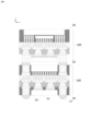
- FIG. 16B shows an example of a semiconductor package in which semiconductor devices 50 and 51 are connected and mounted on both sides of an interposer 100 as an example of the third embodiment.
- the external connection terminals With different heights, it becomes possible to mount the semiconductor device 50 or 51 on both sides of the interposer, thereby improving the degree of freedom in mounting the semiconductor device.
- the underfill 19 or the mold resin 20 may be formed on the semiconductor devices 50 and 51, respectively.
- well-known mounting techniques can be appropriately adopted.
- the manufacturing method of the third embodiment will be described with reference to FIG.
- the same reference numerals are given to the same or equivalent components as in the above-described first embodiment, the description thereof will be simplified or omitted, and only the differences from the first embodiment will be described.
- the first half of the manufacturing method of the third embodiment can be produced by the same steps as those shown in FIGS.
- the interposer, the semiconductor package, and the manufacturing method thereof according to the third embodiment will be described with reference to FIGS.
- FIG. 17(l) corresponds to FIG. 8(l) of the first embodiment, and can be produced by the same method as in the first embodiment up to this step.
- FIG. 17(m) is a cross-sectional view of the interposer 100 from which the resist 3 and the support substrate 1 shown in FIG. 17(l) are removed. Note that FIG. 17(m) is shown upside down with respect to FIG. 17(l) for the sake of convenience.
- the metal layer 2 and the thin copper foil 13 of the carrier copper foil are formed on the first outer layer structure 5 and the second outer layer structure 11, respectively.
- FIG. 17(n) is a diagram for explaining the process of forming the first connection terminal 16 and the second connection terminal 17.
- a resist pattern 3 is formed on both sides of the metal layer 2 and the thin copper foil 13 of the carrier copper foil, electrolytic Ni plating and electrolytic Sn—Ag plating serving as solder are formed to form the first connection.
- a terminal 16 and a second connection terminal 17 can be formed.
- external connection terminals may be formed on each side by forming a protective layer on one side and forming a resist 3 on the other side. Furthermore, it is also possible to form a protective sheet on one side after forming resist patterns on both sides and then electroplating one side at a time.
- the electroplating method and the resist pattern forming method can be appropriately selected from known pattern forming methods, and are not limited to the above methods. Further, after this step, the solder layer may be heated in a reflow furnace to form round bumps.
- FIG. 18(o) is a diagram for explaining the process of forming the projecting electrodes 22 and 23.
- the respective Any shape can be formed by changing the value of the current flowing through the seed layer.
- the formed thickness and volume are greatly different, it is also possible to form resist patterns on both sides, form a protective sheet on one side, and then perform electrolytic plating on each side.
- the electroplating method and the resist pattern forming method can be appropriately selected from known pattern forming methods, and are not limited to the above methods.
- the solder layer may be heated in a reflow furnace to form round bumps.
- FIG. 18(p) is a diagram showing the interposer 100 in the third embodiment. After removing the resist 3 from the substrate of FIG. 18(o), the metal layer 2 and the thin copper foil layer of the carrier copper foil are removed by etching. Further, by heating the solder layer in a reflow furnace to form round bumps, the interposer 100 in the third embodiment can be obtained.
- a semiconductor device can be stacked and mounted above the first outer layer structure 5 by utilizing the steps obtained by the projecting electrodes. is possible, and the SiP integration rate can be further improved.
- the fourth embodiment is a semiconductor package in which a semiconductor device is mounted on the interposer of the third embodiment. It differs from the first embodiment in that it is possible to stack and mount semiconductor devices above the first outer layer structure 5 and below the second outer layer structure 11 using the protruding electrodes in the third embodiment. . Furthermore, in the fourth embodiment, the interposers 100 can be stacked on each other using projecting electrodes, which is also different from the first embodiment.
- FIG. 19(a) is a fourth embodiment of the interposer in this embodiment.
- FIG. 19(a) forms the first connection terminal 16 and the second connection terminal 17 by electrolytic Ni and electrolytic Sn—Ag plating on the projecting electrodes 22 and 23 described in FIG. 18(o) of the third embodiment. The difference is that they are not.
- FIG. 19(b) shows a process after mounting the semiconductor devices 50 and 51 on the first connection terminals 16 and the second connection terminals 17 on which the projecting electrodes are not formed in the interposer 100 of the fourth embodiment.
- FIG. 20(c) shows the semiconductor package in this embodiment after molding resin is formed on both sides of the interposer on which the semiconductor device of FIG. 19(b) is mounted.
- FIG. 20(d) shows the semiconductor package shown in FIG. 20(c) by grinding the mold resin formed on the outermost surface of the semiconductor package so that the protruding electrodes 22 and 23 and the semiconductor device 50, 51 shows an exposed view of the surface of 51.
- FIG. 21 is a diagram showing an example of a semiconductor package in which a plurality of semiconductor packages are stacked.
- 21 shows a semiconductor package in which the semiconductor package (upper stage) shown in FIG. 16B, which is the third embodiment, is stacked on the semiconductor package (lower stage) shown in FIG. there is
- such lamination of interposers and lamination of semiconductor devices is not limited to the combination described above, and any number of lamination can be configured within the range of physical processing, and the types of semiconductor devices and interposers to be combined can be varied. Needless to say, it can be arbitrarily selected.
- the interposer laminated structure can be realized by using the interposer according to the present embodiment, which can contribute to the improvement of the functionality of the semiconductor package by advanced SiP.
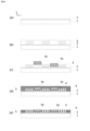
- FIG. 25(a) is a cross-sectional schematic diagram of an interposer 100 in which a built-in component 70 is embedded in the interposer 100 of the fifth embodiment.
- FIG. 25B is a cross-sectional schematic diagram of a semiconductor package 150 in which the semiconductor devices 50 and 51 are mounted on the interposer 100 of the fifth embodiment.
- the fifth embodiment differs from the first embodiment in that a built-in component 70 is embedded.
- the built-in component 70 may be electrically connected to the first connection terminals 16 on the upper surface. Alternatively, if there are built-in component connection terminals (not shown) on the bottom surface of the built-in component 70, they are electrically connected to the first connection terminal 16 or the second connection terminal 17 through the via 9 and the wiring 10 of the inner layer structure 7. may be Alternatively, if there are connection terminals on both the upper surface and the lower surface of the built-in component 70, both connection terminals may be electrically connected at the same time.
- the size of the built-in component 70 is preferably at least smaller than that of the interposer 100 and is of a size that does not impose restrictions on the mounting of the semiconductor device and wiring routing, but is not limited by this embodiment.
- the number of embedded parts 70 to be embedded is preferably such that it does not impose restrictions on the mounting of the semiconductor device and the routing of wiring, but is not limited by this embodiment.
- the thickness of the built-in component 70 is desirably thinner than that of the interposer 100 at least when built into the interposer 100 . It is desirable that the thickness is such that it does not impose restrictions on the mounting of the semiconductor device or the routing of the wiring, but it is not limited by this embodiment. For example, it is desirable that the thickness of the built-in component 70 is 10 ⁇ m or more and 1 mm or less.
- the thickness of the built-in part 70 is less than 10 ⁇ m, even if a highly rigid material, which will be described later, is used, not only will the interposer itself not be able to exhibit sufficient rigidity, but there is also a risk that the built-in part will be damaged. There is If the thickness of the built-in part 70 is more than 1 mm, the thickness of the interposer itself needs to be increased, which not only increases manufacturing time and cost, but also makes it difficult to incorporate the built-in part inside the interposer.
- the built-in component 70 can be selected from components based on silicon, ceramic, glass, and compound semiconductors.
- the silicon-based parts are, for example, capacitors, inductors, chip parts having rewiring functions, and semiconductor chips having arithmetic functions on silicon wafers. Additionally, the silicon-based component may be a functional module containing one or more of these elements.
- Ceramic-based component are, for example, components having independent functions such as capacitors, inductors, and wiring. Furthermore, the ceramic-based component may be a functional module containing one or more of these elements.
- Ceramic materials are also, for example, alumina, yttria, cordierite, cermet, sapphire, zirconia, steatite, forsterite, silicon carbide, aluminum nitride, silicon nitride, LTCC (Low Temperature Co-fired Ceramics), but others material.
- glass-based parts are, for example, parts having independent functions such as capacitors, inductors, and wiring. Additionally, the glass-based component may be a functional module containing one or more of these elements. Examples of glass materials include soda lime glass, borosilicate glass, crystallized glass, and quartz glass, but other materials may be used.
- Components based on compound semiconductors include, for example, high-frequency devices and optical semiconductors containing compound semiconductors such as GaAs, InP, and InGaAlP, LEDs and laser diodes containing InGaN, and power semiconductor materials containing SiC and GaN. Other materials may be used.
- a typical insulating resin material has a linear thermal expansion coefficient CTE of 30 to 100 ppm/K and an elastic modulus of 1 to 30 GPa.
- silicon, ceramic, glass, and compound semiconductor materials have a CTE of 12 ppm/K or less, and an elastic modulus of 60 to 470 GPa, and have low thermal expansion and high elasticity as compared with insulating resin materials. Accordingly, by embedding the component in the interposer 100, the interposer 100 can be provided with high thermal dimensional stability and rigidity at the same time.
- thermal dimensional stability refers to the property that the interposer is resistant to thermal deformation due to thermal cycles.
- FIG. 26(a) is a process corresponding to FIG. 7(a) of the first embodiment.
- a supporting substrate is prepared as shown in FIG. 26(a). The same support substrate as described in the first embodiment can be used.
- FIG. 26(b) is a diagram showing the process of forming the resist pattern 3 on the portion other than the portion where the built-in component 70 is mounted.
- a resist pattern 3 is formed on the portion other than the portion where the built-in component 70 is mounted.
- a liquid resist is formed with a thickness of 120 ⁇ m, and openings are formed so that columnar pads can be formed with the same pitch and diameter as in the first embodiment.
- FIG. 26(c) is a diagram in which the conductive member 4 is formed with an average thickness of 120 ⁇ m by electrolytic copper plating, the resist pattern 3 is removed, and the built-in component 70 is mounted.
- a silicon capacitor is mounted as the built-in component 70 .
- the silicon capacitor has a total thickness of 120 ⁇ m and a size of 5 mm ⁇ 5 mm square, for example.
- the silicon capacitor is fixed to the support substrate with an adhesive, but other methods may be used.
- FIG. 26(d) is a step corresponding to FIG. 7(d).
- FIG. 26(d) is a diagram showing the process of forming the second insulating resin layer 6, which will become the first outer layer structure 5, by vacuum lamination using a 150 ⁇ m thick film mold resin.
- the second insulating resin layer 6 is formed by vacuum lamination using a film-like molding resin having a thickness of 150 ⁇ m.
- FIG. 26(e) is a diagram showing a process of polishing the mold resin and the Si base material of the silicon capacitor using a grinder to expose a part of the built-in component 70 and the conductive member 4.
- the mold resin and the Si base material of the silicon capacitor are ground using a grinder to expose part of the built-in component 70 and the conductive member 4.
- the second insulating resin layer 6 that forms the first outer layer structure 5 is polished, and the first outer layer structure 5 is adjusted and polished to a thickness of 100 ⁇ m.
- the method of exposing a portion of the built-in component 70 and the conductive member 4 is not limited to the method of this embodiment, and similar to FIG. It may be CMP.
- the conductive member 4 that serves as a pad is formed in the second insulating resin layer 6 of the first outer layer structure 5 .
- the inner layer structure 7 is formed in the same manner as described in FIGS. 8(f) to (i) of the first embodiment, and the same as described in FIGS. 25(a) by forming the second outer layer structure 11 and further forming the first connection terminal 16 and the second connection terminal 17 by the method shown in FIGS. 9(n) to 10(q). It is possible to form the interposer 100 in a modification of .
- the semiconductor package 150 can be manufactured using the inspection method, the semiconductor device assembly method, and the repair method shown in FIGS. 12(a) to 13(e) of the first embodiment.
- the interposer 100 shown in FIG. 27( a ) is a diagram showing a modification of the fifth embodiment in which the built-in component 70 is accommodated on the lower surface of the first outer layer structure 5 and inside the inner layer structure 7 .
- the method of manufacturing the interposer 100 shown in FIG. 27(a) is the same as that of the first embodiment shown in FIGS. .
- FIG.7(e) is transferred to FIG.27(b), and it demonstrates.
- On the second insulating resin layer 6 shown in FIG. 27(b), a built-in component 70 is mounted so as to be electrically connected to the conductive member 4 as shown in FIG. 27(c).
- a conductive paste may be formed on the terminal for connection, or solder connection may be used.
- an underfill may be provided in the gap between the built-in component 70 and the first outer layer structure 5 .
- a substrate having four inner layer structures 7 shown in FIG. 27(d) is obtained by the same method as shown in FIGS. 8(f) to (i) of the first embodiment.
- the built-in component 70 shown in FIG. 27(d) may be electrically connected to the first connection terminal through the conductive member 4.
- connection terminals (not shown) are provided on the upper surface of the built-in component 70 shown in FIGS. As shown in FIG.
- connecting terminals (not shown) on the upper surface of the internal component 70 and the wiring 10 of the inner layer structure are electrically connected via the pads 15 and the vias 9, whereby the first and second connections are established. It may be electrically connected to the terminal. Alternatively, if there are connection terminals on both the upper surface and the lower surface of the built-in component 70, both connection terminals may be electrically connected at the same time.
- FIG. 28( a ) is a modified example in which the built-in component 70 is housed inside the second outer layer structure 11 .
- the manufacturing method of the interposer 100 of FIG. 28(a) is the same as that of FIGS. 7(a) to (e) and FIGS. 8(f) to (i) of the first embodiment.
- FIG. 8(i) will be transferred to FIG. 28(b) for explanation.
- FIG. 28(b) is a diagram after four layers of the inner layer structure 7 are formed, like FIG. 8(i) of the first embodiment. Subsequently, the built-in component 70 is mounted on a part of the wiring 10 as shown in FIG. 28(c).
- FIG. 28(d) shows a diagram in which the steps of FIGS. 8(j) to 9(m) of the first embodiment are performed.
- the interposer 100 in this modification shown in FIG. 27(a) can be formed by the same method as shown in FIGS. 9(n) to 10(q).
- FIG. 25(a) which is the fifth embodiment in this modified example, FIGS. It may be combined with a modification in which terminals 17 are partitioned using a solder resist. Furthermore, as described with reference to FIG. 5, it may be combined with a structure in which two or more layers of the first outer layer structure 5 are formed. Moreover, as described with reference to FIG. 6, it may be combined with a structure in which the second outer layer structure 11 is formed of two or more layers. Alternatively, a method of forming vias in the first outer layer structure 5 by laser processing in the manufacturing method shown in FIG. 11 may be employed.
- the interposer 100 of the present embodiment it is possible to contribute to the improvement of the self-sustainability of the interposer 100 by embedding a part whose base material is a highly rigid material in the interposer. As a result, the rigidity of the interposer 100 can be improved, and at the same time, it is possible to add the function of the built-in parts to the interposer, which has only the function of rewiring, and contribute to the enhancement of functionality.
- interposer 100 of this embodiment built-in components can be mounted very close to the semiconductor device, effectively reducing signal and power noise and stabilizing the power supply to the chip.
- the interposer by providing an interposer that can be independently transported by itself without a support, the following five effects are achieved. 1) Since the interposer itself has the rigidity to withstand the electrical inspection without having a support substrate, it is possible to guarantee the electrical inspection of the interposer itself before mounting the semiconductor device. As a result, it is possible to eliminate defective semiconductor packages caused by mounting an expensive semiconductor device on a defective interposer.
- interposer of the present disclosure can exist independently of the support or FC-BGA, it is possible to mount the semiconductor package on the FC-BGA or motherboard, greatly improving the degree of mounting freedom. can be made
- the present invention is not limited to the above-described embodiments, and various modifications are possible without departing from the gist of the present invention.
- the first outer layer structure is formed first with respect to the second outer layer structure, but the order of formation is not limited in any way.
- the second outer layer structure (connection side to BGA or motherboard) may be formed first, and the first outer layer structure may be formed later.
- the manufacturing method of the present disclosure may be manufactured in a state in which one interposer is formed on a square panel or a circular wafer in which a plurality of interposers are arranged.
- the shape of the manufacturing panel and the thickness and size of the support substrate described in the present disclosure are not limited at all, and appropriate shapes and sizes can be adopted.
- an inner layer structure including at least one inner layer wiring layer; a first outer layer structure disposed on the first surface of the inner layer structure and having higher rigidity than the inner layer structure;
- an interposer comprising a second outer layer structure disposed on the second surface of the inner layer structure and having higher rigidity than the inner layer structure
- the inner wiring layer includes wiring arranged on the surface of the first insulating resin layer and a conductive member connected to the wiring and penetrating the first insulating resin layer
- the first outer layer structure and the second outer layer structure each include a second insulating resin layer and a conductive member penetrating the second insulating resin layer
- the first outer layer structure and/or the second outer layer structure is a terminal that can be connected to a semiconductor device and that can be electrically tested on a surface opposite to the surface that is connected to the inner layer structure.
- An interposer comprising: (Aspect 2) The interposer according to claim 1, The interposer, wherein the first outer layer structure and the second outer layer structure cover at least the first surface and the second surface of the inner layer structure. (Aspect 3) In the interposer according to aspect 1 or 2, The first insulating resin layer is a photosensitive resin, The interposer, wherein the second insulating resin layer is a non-photosensitive resin containing a filler. (Aspect 4) In the interposer according to any one of aspects 1 to 3, An interposer, wherein the first insulating resin layer and the second insulating resin layer are made of a non-photosensitive resin.
- the second insulating resin layer includes any one of a prepreg, a built-up resin, and a mold resin having physical properties such as an elastic modulus of 5 GPa or more and a CTE of 20 ppm or less.
- the second insulating resin layer includes any one of a prepreg, a built-up resin, and a mold resin having physical properties such as an elastic modulus of 5 GPa or more and a CTE of 20 ppm or less.
- An interposer, wherein the sum of the thicknesses of the first outer layer structure and the second outer layer structure is greater than the thickness of the inner layer structure.
- An interposer, wherein either the first outer layer structure or the second outer layer structure also covers the side surface of the inner layer structure.
- a projecting electrode is provided above the conductive member that penetrates the first insulating resin layer and/or below the conductive member that penetrates the second insulating resin layer, The interposer, wherein the projecting electrodes can be used as connection terminals.
- ⁇ Measurement method> The distance L between the fulcrums is 66 mm, the indenter radius r1 is 2 mm, and the inter-indenter distance L' is 22 mm with respect to the vertical and horizontal surfaces of the test piece with dimensions of 80 mm long x 15 mm wide x h (thickness of the test piece) mm.
- a four-point bending test is performed at a test speed V calculated by the following formula. (Mode 10)
- the interposer according to aspect 9 when the thickness h of the test piece is 300 ⁇ m, the measured load is 5.7 N and the amount of deflection is 7 mm when the test speed V is 30 mm/sec. interposer.
- a semiconductor package wherein a semiconductor device mounted on a connection terminal formed on a projecting electrode and a semiconductor device mounted on a connection terminal on which the projecting electrode is not formed are stacked and mounted.
- a semiconductor package wherein a plurality of said semiconductor packages are connected by projecting electrodes and stacked.
Abstract
The purpose of the present invention is to provide a system in package (SiP) in which the quality of an interposer can be checked before a semiconductor device is mounted thereon, and that has high yield. Accordingly, provided is an interposer comprising: an inner-layer structure which includes at least one inner-layer wiring layer; a first outer-layer structure which is disposed on a first surface of the inner-layer structure and has higher stiffness than the inner-layer structure; and a second outer-layer structure which is disposed on a second surface of the inner-layer structure and has higher stiffness than the inner-layer structure. The inner-layer wiring layer comprises a wire disposed on a surface of a first insulating resin layer and a conductive member which connects to the wire and penetrates through the first insulating resin layer. The first outer-layer structure and the second outer-layer structure each comprises a second insulating resin layer and a conductive member penetrating through the second insulating resin. A terminal that can be connected to a semiconductor device and allows for electric testing is formed on a surface of the first outer-layer structure and/or the second outer-layer structure on the opposite side to the surface thereof connected to the inner-layer structure.
Description
本発明は半導体装置を実装するためのインターポーザ、インターポーザに半導体装置を実装した半導体パッケージ及びそれらの製造方法に関する。
The present invention relates to an interposer for mounting a semiconductor device, a semiconductor package in which the semiconductor device is mounted on the interposer, and a method of manufacturing them.
近年では、複数個の異種半導体装置(半導体チップ)をインターポーザ上に搭載し、一つの高機能半導体パッケージとする、SiP(System In Package)が実用化されている。この手法によればプロセスコストを増大させることなく、高機能化された一つの半導体装置である「半導体パッケージ」を得ることができる。
In recent years, SiP (System In Package) has been put into practical use, in which a plurality of different types of semiconductor devices (semiconductor chips) are mounted on an interposer to form a single high-performance semiconductor package. According to this technique, it is possible to obtain a "semiconductor package", which is a highly functional semiconductor device, without increasing the process cost.
また、上記のSiPに搭載される半導体装置としては、積層DRAMであるHBM(High Bandwidth Memory)が多く用いられる傾向にある。HBMは、一般的に接続端子のピッチは55μm程度の狭ピッチであり、インターポーザにも同程度の接続端子を形成する必要がある。
In addition, HBM (High Bandwidth Memory), which is a stacked DRAM, tends to be widely used as a semiconductor device mounted on the SiP. The HBM generally has a narrow pitch of about 55 μm between the connection terminals, and it is necessary to form the same degree of connection terminals on the interposer.
また、上記のようなインターポーザは、FC-BGAに接続されることとなるが、FC-BGAのCTE(Coefficient of Thermal Expansion)は18ppm/℃程度であり、半導体チップのCTE3ppm/℃と比較すると高い。このため、インターポーザには、半導体チップとFC-BGAの間のCTEのミスマッチを緩和する機能を有することが求められる。
さらに、半導体パッケージとしての組み立ての利便性のためには、半導体装置をインターポーザに実装した後に、これをFC-BGAに実装できることが望ましい。このため、インターポーザはFC-BGAと別個に自立する単体として存在できる必要がある。 In addition, the interposer as described above is connected to the FC-BGA, and the CTE (Coefficient of Thermal Expansion) of the FC-BGA is about 18 ppm/°C, which is higher than the CTE of the semiconductor chip, which is 3 ppm/°C. . Therefore, the interposer is required to have a function of alleviating the CTE mismatch between the semiconductor chip and the FC-BGA.
Furthermore, for the convenience of assembly as a semiconductor package, it is desirable to be able to mount the semiconductor device on the interposer and then mount it on the FC-BGA. For this reason, the interposer must be able to exist as an independent unit separate from the FC-BGA.
特許文献1においては、インターポーザの反りを抑制するために、半導体パッケージ(1)の製造方法として、板状の第1補強部材(5A)と、第1導体パターン配線基板用積層体(2A)と、第2導体パターン(224)上に配置された板状の第2補強部材(4A)とを有する積層体(20)を用意する工程と、積層体(20)を加熱して前記絶縁層を熱硬化する工程と、第1補強部材(5A)の一部を選択的に除去して、第1導体パターン(224)を露出させるための開口部を形成する工程と、第2補強部材(4A)の一部を選択的に除去して第2導体パターン(221)を露出させるための開口部41を形成する工程と第2補強部材(4A)の開口部から露出する第2導体パターン(221)に、半導体素子(3)を接続する工程とを含む技術を開示している。
In Patent Document 1, in order to suppress warpage of the interposer, as a method of manufacturing a semiconductor package (1), a plate-like first reinforcing member (5A) and a first conductor pattern wiring board laminate (2A) are used. and a plate-shaped second reinforcing member (4A) disposed on a second conductor pattern (224); and heating the laminate (20) to remove the insulating layer. a step of thermally curing; a step of selectively removing a portion of the first reinforcing member (5A) to form an opening for exposing the first conductor pattern (224); ) to form an opening 41 for exposing the second conductor pattern (221) and the second conductor pattern (221) exposed from the opening of the second reinforcing member (4A) ) and connecting the semiconductor element (3).
しかし、特許文献1として示すインターポーザは、繊維基材に樹脂組成物を含浸させた構造であるため、形成できるビアの口径は直径50μmが限界となる。また、ビアとビアとのピッチについても130μmが限界となり、積層DRAMであるHBMを搭載することが難しい。
However, since the interposer shown in Patent Document 1 has a structure in which a fiber base material is impregnated with a resin composition, the diameter of vias that can be formed is limited to a diameter of 50 μm. Also, the pitch between vias is limited to 130 μm, making it difficult to mount an HBM, which is a stacked DRAM.
さらに、ファンナウトパッケージやシリコンインターポーザ等の従来のインターポーザ及びこれらを用いた半導体パッケージにおいては、インターポーザ自体を検査した後に半導体装置を実装する工程を経ることが想定されていない。
このため、従来の製造方法では、インターポーザ自体が検査保証されていない状況で、複数個のチップをインターポーザに実装することになる。
その結果、半導体パッケージの歩留まりは、インターポーザの製造不良とチップ実装不良の合算であり、夫々切り分けることができない。 Furthermore, conventional interposers such as fan-out packages and silicon interposers, and semiconductor packages using these interposers, are not supposed to go through a step of mounting a semiconductor device after inspecting the interposer itself.
For this reason, in the conventional manufacturing method, a plurality of chips are mounted on the interposer under the condition that the interposer itself is not guaranteed to be inspected.
As a result, the yield of semiconductor packages is the sum of interposer manufacturing defects and chip mounting defects, and cannot be separated from each other.
具体的には、SiPの製造歩留まりは、簡易的に以下の試算式(1)によって記述できる。
「インターポーザ歩留まり」(YINTERPOSER):(0~1の値)
半導体チップの実装の相乗平均歩留まり(「実装歩留まり」(YASSEMBRY):(0~1の値)
SiPへの半導体装置の搭載個数:N(1以上の整数)
SiPの製造歩留まり(YTOTAL):(0~1の値)
とすると、SiPの製造歩留まりは以下のとおりとなる。
(YTOTAL)=(YINTERPOSER)×(YASSEMBRY)N ・・・・・(1) Specifically, the SiP manufacturing yield can be simply described by the following trial calculation formula (1).
"Interposer Yield" (Y INTERPOSER ): (value between 0 and 1)
Geometric mean yield of semiconductor chip mounting ("mounting yield" (Y ASSEMBRY ): (value between 0 and 1)
Number of semiconductor devices mounted on SiP: N (integer of 1 or more)
SiP manufacturing yield (Y TOTAL ): (value between 0 and 1)
Then, the manufacturing yield of SiP is as follows.
(Y TOTAL ) = (Y INTERPOSER ) x (Y ASSEMBRY ) N (1)
式(1)に記載の通り、SiPの製造歩留まりはインターポーザ収率と、チップ実装の相乗平均歩留まりのチップ数の累乗となる。
ここで、「インターポーザ歩留まり」(YINTERPOSER)及び「実装歩留まり」(YASSEMBRY)がともに90%であり、7個のチップを搭載するSiPの場合
(YINTERPOSER)=(YASSEMBRY)=90%、 N=7・・・・・・(2)
(YTOTAL)=0.97=47.8%・・・・・・・・・・・・・(3)
となり、各プロセス歩留まりが90%としても、SiP全体の製造歩留は極めて低くなる問題を生じる。 As described in equation (1), the SiP manufacturing yield is the power of the interposer yield and the geometric mean yield of chip mounting multiplied by the number of chips.
Here, the "interposer yield" (Y INTERPOSER ) and the "mounting yield" (Y ASSEMBRY ) are both 90%, and in the case of a SiP with seven chips (Y INTERPOSER )=(Y ASSEMBRY )=90%, N=7 (2)
(Y TOTAL )=0.9 7 =47.8% (3)
As a result, even if the yield of each process is 90%, the overall manufacturing yield of SiP is extremely low.
複数の半導体装置を実装して1つの半導体パッケージを構成するSiPでは、個々の半導体装置が検査良品であったとしても、インターポーザの製造不良、実装不良が1か所でもある場合、SiP全体(複数個半導体装置全部)の廃棄に繋がる。この結果、搭載チップ数が増大すると、SiP製造歩留まりは指数関数的に低下し、かつ廃棄される良品チップ数も増大する問題がある。
In a SiP in which a plurality of semiconductor devices are mounted to form a single semiconductor package, even if each individual semiconductor device passes the inspection, if there is even one defect in the manufacturing or mounting of the interposer, the whole SiP (a plurality of This leads to the disposal of all individual semiconductor devices). As a result, when the number of mounted chips increases, the SiP manufacturing yield decreases exponentially, and the number of non-defective chips that are discarded also increases.
さらに、従来の製造方法では、搭載半導体装置全面をモールド樹脂で固めるため、製造不良の存在する個々の半導体装置をリペアのために交換等をすることは不可能となる問題がある。
Furthermore, in the conventional manufacturing method, since the entire surface of the mounted semiconductor device is solidified with mold resin, there is a problem that it is impossible to replace individual semiconductor devices with manufacturing defects for repair.
そこで、本発明では、60μm以下の狭ピッチの半導体装置の接続用端子が形成可能であって、半導体装置の実装前にインターポーザ自体を電気検査可能なインターポーザを提供することを目的とする。
Therefore, an object of the present invention is to provide an interposer capable of forming terminals for connection of a semiconductor device with a narrow pitch of 60 μm or less, and allowing electrical inspection of the interposer itself before mounting the semiconductor device.
上記の課題を解決するため、代表的な本発明のインターポーザの一つは、
少なくとも1層の内層配線層を含む内層構造体と、
前記内層構造体の第1主面上に配置され、前記内層構造体よりも剛性の高い第1外層構造体と、
前記内層構造体の第2主面上に配置され、前記内層構造体よりも剛性の高い第2外層構造体を備えるインターポーザにおいて、
前記内層配線層は、第1絶縁樹脂層の表面に配置された配線及び前記配線に接続し、前記第1絶縁樹脂層を貫通する導電部材を備えており、
前記第1外層構造体及び前記第2外層構造体は、第2絶縁樹脂層と前記第2絶縁樹脂を貫通する導電部材を備えており、
前記第1外層構造体及び/または前記第2外層構造体は、前記内層構造体に接続されている面と反対側の面において、半導体装置と接続可能であり、かつ、電気検査が可能な端子を備えている。 In order to solve the above problems, one representative interposer of the present invention is
an inner layer structure including at least one inner layer wiring layer;
a first outer layer structure disposed on the first main surface of the inner layer structure and having higher rigidity than the inner layer structure;
In an interposer comprising a second outer layer structure disposed on the second main surface of the inner layer structure and having higher rigidity than the inner layer structure,
The inner wiring layer includes wiring arranged on the surface of the first insulating resin layer and a conductive member connected to the wiring and penetrating the first insulating resin layer,
The first outer layer structure and the second outer layer structure each include a second insulating resin layer and a conductive member penetrating through the second insulating resin,
The first outer layer structure and/or the second outer layer structure is a terminal that can be connected to a semiconductor device and that can be electrically tested on a surface opposite to the surface that is connected to the inner layer structure. It has
本発明によれば、60μm以下の狭ピッチの半導体装置の接続用端子が形成可能であって、半導体装置の実装前にインターポーザ自体を電気検査可能なインターポーザを提供することができる。
上記した以外の課題、構成および効果は、以下の実施をするための形態における説明により明らかにされる。 According to the present invention, it is possible to provide an interposer capable of forming connection terminals of a semiconductor device with a narrow pitch of 60 μm or less and being electrically inspectable before mounting the semiconductor device.
Problems, configurations, and effects other than those described above will be clarified by the description in the following embodiments.
以下、図面を参照して、本発明の実施形態について説明する。なお、この実施形態により本発明が限定されるものではない。また、図面の記載において、同一部分には同一の符号を付して示している。第1および第2の呼称は特に順序や構成を限定するものではなく、説明便宜上規定するものである。
Hereinafter, embodiments of the present invention will be described with reference to the drawings. It should be noted that the present invention is not limited by this embodiment. Moreover, in the description of the drawings, the same parts are denoted by the same reference numerals. The first and second names do not particularly limit the order or configuration, but are defined for convenience of explanation.
図面において示す各構成要素の位置、大きさ、形状、範囲などは、発明の理解を容易にするため、実際の位置、大きさ、形状、範囲などを表していない場合がある。このため、本発明は、必ずしも、図面に開示された位置、大きさ、形状、範囲などに限定されない。
The position, size, shape, range, etc. of each component shown in the drawings may not represent the actual position, size, shape, range, etc. in order to facilitate the understanding of the invention. As such, the present invention is not necessarily limited to the locations, sizes, shapes, extents, etc., disclosed in the drawings.
なお、本開示において、「面」とは、板状部材の面のみならず、板状部材に含まれる層について、板状部材の面と略平行な層の界面も指すことがある。また、「上面」、「下面」とは、板状部材や板状部材に含まれる層を図示した場合の、図面上の上方又は下方に示される面を意味する。なお、「上面」、「下面」については、「第1面」、「第2面」と称することもある。
In the present disclosure, the term "surface" may refer not only to the surface of the plate-like member, but also to the interface between the layers included in the plate-like member that is substantially parallel to the surface of the plate-like member. In addition, the terms "upper surface" and "lower surface" refer to the upper or lower surface of the drawing when a plate-like member or a layer included in the plate-like member is illustrated. The "upper surface" and "lower surface" may also be referred to as "first surface" and "second surface".
また、「側面」とは、板状部材や板状部材に含まれる層における面や層の厚みの部分を意味する。さらに、面の一部及び側面を合わせて「端部」ということがある。
また、「上方」とは、板状部材又は層を水平に載置した場合の垂直上方の方向を意味する。さらに、「上方」及びこれと反対の「下方」については、これらを「Z軸プラス方向」、「Z軸マイナス方向」ということがあり、水平方向については、「X軸方向」、「Y軸方向」ということがある。 In addition, the “side surface” means a surface of a plate-like member or a layer included in the plate-like member or a portion of the thickness of the layer. Furthermore, a part of a surface and a side surface may be collectively referred to as an "end".
Moreover, "upper" means the vertically upward direction when the plate-like member or layer is placed horizontally. Further, "upward" and "downward" opposite to this are sometimes referred to as "Z-axis positive direction" and "Z-axis negative direction", and horizontal directions are referred to as "X-axis direction" and "Y-axis direction". It is sometimes called "direction".
また、「平面形状」、「平面視」とは、上方から面又は層を視認した場合の形状を意味する。さらに、「断面形状」、「断面視」とは、板状部材又は層を特定の方向で切断した場合の水平方向から視認した場合の形状を意味する。
さらに、「中心部」とは、面又は層の周辺部ではない中心部を意味する。そして、「中心方向」とは、面又は層の周辺部から面又は層の平面形状における中心に向かう方向を意味する。 Further, "planar shape" and "planar view" mean the shape when a surface or layer is viewed from above. Furthermore, the terms "cross-sectional shape" and "cross-sectional view" mean the shape of a plate-like member or layer cut in a specific direction and viewed from the horizontal direction.
Further, "core" means the core of a face or layer, but not the periphery. The term "central direction" means a direction from the periphery of a surface or layer toward the center of the planar shape of the surface or layer.
(第1実施形態)
<インターポーザの構造>
図1(a)は本発明における第1実施形態のインターポーザ100の断面模式図の例である。図1(b)は第1実施形態のインターポーザ100に、半導体装置50および51を搭載した半導体パッケージ150の断面模式図である。
なお、本開示では、インターポーザ100の上下の面について、半導体装置50および51が搭載される側を「第1面側」と称し、インターポーザ100がマザーボードあるいはFC-BGAへの接続する側を「第2面側」と称する。 (First embodiment)
<Interposer structure>
FIG. 1(a) is an example of a schematic cross-sectional view of aninterposer 100 according to a first embodiment of the present invention. FIG. 1B is a schematic sectional view of a semiconductor package 150 in which semiconductor devices 50 and 51 are mounted on the interposer 100 of the first embodiment.
In the present disclosure, regarding the top and bottom surfaces of theinterposer 100, the side on which the semiconductor devices 50 and 51 are mounted is referred to as the "first surface side", and the side where the interposer 100 is connected to the motherboard or FC-BGA is referred to as the "first surface side." 2 sides".
<インターポーザの構造>
図1(a)は本発明における第1実施形態のインターポーザ100の断面模式図の例である。図1(b)は第1実施形態のインターポーザ100に、半導体装置50および51を搭載した半導体パッケージ150の断面模式図である。
なお、本開示では、インターポーザ100の上下の面について、半導体装置50および51が搭載される側を「第1面側」と称し、インターポーザ100がマザーボードあるいはFC-BGAへの接続する側を「第2面側」と称する。 (First embodiment)
<Interposer structure>
FIG. 1(a) is an example of a schematic cross-sectional view of an
In the present disclosure, regarding the top and bottom surfaces of the
本実施形態ではまた、第2外層構造体11の第2面側に第2接続端子17が配置されている。第2接続端子17はFC-BGA基板あるいはマザーボードへの接続端子となる。
図1(a)におけるインターポーザ100は、主に、第1外層構造体5、内層構造体7、第2外層構造体11から構成される。
第1外層構造体5は、内層構造体7の上方、つまりZ軸プラス方向に配置されている。また、第1外層構造体5は第2絶縁樹脂層6で形成されており、第2絶縁樹脂層6には、Z軸方向に第2絶縁樹脂層6を貫通する導電部材4が形成されている。第2絶縁樹脂層6を貫通する導電部材4は、第1外層構造体5の外部接続端子のパッドとして機能することができる。
また、第1外層構造体5の第1面側に第1接続端子16が配置されている。 Also in this embodiment, thesecond connection terminals 17 are arranged on the second surface side of the second outer layer structure 11 . The second connection terminal 17 serves as a connection terminal to the FC-BGA board or motherboard.
Theinterposer 100 in FIG. 1( a ) is mainly composed of a first outer layer structure 5 , an inner layer structure 7 and a second outer layer structure 11 .
The firstouter layer structure 5 is arranged above the inner layer structure 7, that is, in the positive Z-axis direction. The first outer layer structure 5 is formed of a second insulating resin layer 6, and the second insulating resin layer 6 is formed with a conductive member 4 penetrating through the second insulating resin layer 6 in the Z-axis direction. there is The conductive member 4 penetrating the second insulating resin layer 6 can function as a pad for the external connection terminal of the first outer layer structure 5 .
Afirst connection terminal 16 is arranged on the first surface side of the first outer layer structure 5 .
図1(a)におけるインターポーザ100は、主に、第1外層構造体5、内層構造体7、第2外層構造体11から構成される。
第1外層構造体5は、内層構造体7の上方、つまりZ軸プラス方向に配置されている。また、第1外層構造体5は第2絶縁樹脂層6で形成されており、第2絶縁樹脂層6には、Z軸方向に第2絶縁樹脂層6を貫通する導電部材4が形成されている。第2絶縁樹脂層6を貫通する導電部材4は、第1外層構造体5の外部接続端子のパッドとして機能することができる。
また、第1外層構造体5の第1面側に第1接続端子16が配置されている。 Also in this embodiment, the
The
The first
A
内層構造体7は、第1外層構造体5及び第2外層構造体11との間に配置されている。
内層構造体7は、少なくとも1層の内層配線層を備えており、内層配線層は、第1絶縁樹脂層8、第1絶縁樹脂層の表面に配置された配線10、及び、前記配線10に接続し、第1絶縁樹脂層をZ軸方向に貫通する導電部材を備えている。また、第1絶縁樹脂層を貫通する導電部材は、内層配線層のビア9として機能することができる。
また、第1外層構造体5の第1面側には、第1接続端子(半田)16が配置されている。 Theinner layer structure 7 is arranged between the first outer layer structure 5 and the second outer layer structure 11 .
Theinner layer structure 7 has at least one inner layer wiring layer, and the inner layer wiring layer includes a first insulating resin layer 8, a wiring 10 disposed on the surface of the first insulating resin layer, and a wiring 10 for the wiring 10. A conductive member is provided that connects and penetrates the first insulating resin layer in the Z-axis direction. Also, the conductive member penetrating the first insulating resin layer can function as the via 9 of the inner wiring layer.
A first connection terminal (solder) 16 is arranged on the first surface side of the firstouter layer structure 5 .
内層構造体7は、少なくとも1層の内層配線層を備えており、内層配線層は、第1絶縁樹脂層8、第1絶縁樹脂層の表面に配置された配線10、及び、前記配線10に接続し、第1絶縁樹脂層をZ軸方向に貫通する導電部材を備えている。また、第1絶縁樹脂層を貫通する導電部材は、内層配線層のビア9として機能することができる。
また、第1外層構造体5の第1面側には、第1接続端子(半田)16が配置されている。 The
The
A first connection terminal (solder) 16 is arranged on the first surface side of the first
第2外層構造体11は、内層構造体7の下方、つまりZ軸マイナス方向に配置されている。
また、第2外層構造体11は第2絶縁樹脂層12で形成されており、第2絶縁樹脂層12には、Z軸方向に第2絶縁樹脂層12を貫通する導電部材が形成されている。第2絶縁樹脂層12を貫通する導電部材は、内層構造体7の最外層の配線層と接続するとともに、第2外層構造体11の外部接続端子のパッドとして機能することができる。
また、第2外層構造体11の第2面側には、外部接続端子のパッド15及び第2接続端子(半田)17が配置されている。 The secondouter layer structure 11 is arranged below the inner layer structure 7, that is, in the negative Z-axis direction.
In addition, the secondouter layer structure 11 is formed of a second insulating resin layer 12, and a conductive member is formed in the second insulating resin layer 12 so as to penetrate the second insulating resin layer 12 in the Z-axis direction. . The conductive member penetrating the second insulating resin layer 12 is connected to the outermost wiring layer of the inner layer structure 7 and can function as a pad for the external connection terminal of the second outer layer structure 11 .
Also,pads 15 of external connection terminals and second connection terminals (solder) 17 are arranged on the second surface side of the second outer layer structure 11 .
また、第2外層構造体11は第2絶縁樹脂層12で形成されており、第2絶縁樹脂層12には、Z軸方向に第2絶縁樹脂層12を貫通する導電部材が形成されている。第2絶縁樹脂層12を貫通する導電部材は、内層構造体7の最外層の配線層と接続するとともに、第2外層構造体11の外部接続端子のパッドとして機能することができる。
また、第2外層構造体11の第2面側には、外部接続端子のパッド15及び第2接続端子(半田)17が配置されている。 The second
In addition, the second
Also,
なお、インターポーザ100のZ軸方向の厚さは、内層構造体7、第1外層構造体5および第2外層構造体11を含む総厚が50μm以上であることが望ましい。
また、本実施形態におけるインターポーザ100の第1外層構造体5及び第2外層構造体11の厚みは、本実施形態で採用する厚さに限定されるものではないが、第1外層構造体5及び第2外層構造体11が内層構造体7に比較して物理的剛性が高い場合には、第1外層構造体5及び第2外層構造体11の厚みの和が内層構造体7よりも厚いことが望ましい。すなわち第1外層構造体5と第2外層構造体11は、インターポーザ100の総厚の半分以上あることが望ましい。 As for the thickness of theinterposer 100 in the Z-axis direction, the total thickness including the inner layer structure 7, the first outer layer structure 5 and the second outer layer structure 11 is preferably 50 μm or more.
In addition, the thicknesses of the firstouter layer structure 5 and the second outer layer structure 11 of the interposer 100 in the present embodiment are not limited to the thicknesses employed in the present embodiment. When the second outer layer structure 11 has higher physical rigidity than the inner layer structure 7, the sum of the thicknesses of the first outer layer structure 5 and the second outer layer structure 11 is thicker than the inner layer structure 7. is desirable. That is, it is desirable that the thickness of the first outer layer structure 5 and the second outer layer structure 11 be more than half of the total thickness of the interposer 100 .
また、本実施形態におけるインターポーザ100の第1外層構造体5及び第2外層構造体11の厚みは、本実施形態で採用する厚さに限定されるものではないが、第1外層構造体5及び第2外層構造体11が内層構造体7に比較して物理的剛性が高い場合には、第1外層構造体5及び第2外層構造体11の厚みの和が内層構造体7よりも厚いことが望ましい。すなわち第1外層構造体5と第2外層構造体11は、インターポーザ100の総厚の半分以上あることが望ましい。 As for the thickness of the
In addition, the thicknesses of the first
<半導体パッケージの構造>
図1(b)は、図1(a)で説明したインターポーザ100の第1面側に半導体装置50,51をアンダーフィル19及びモールド樹脂20によって固定した半導体パッケージ150である。 <Semiconductor package structure>
FIG. 1B shows asemiconductor package 150 in which semiconductor devices 50 and 51 are fixed to the first surface side of the interposer 100 explained in FIG.
図1(b)は、図1(a)で説明したインターポーザ100の第1面側に半導体装置50,51をアンダーフィル19及びモールド樹脂20によって固定した半導体パッケージ150である。 <Semiconductor package structure>
FIG. 1B shows a
なお、第1接続端子16、および第2接続端子17は半田であるが、本発明により半田種類や半田組成は限定されず公知の導電材料を用いることができる。また、図1(a)、図1(b)における第1接続端子16は、第1外層構造体5の導電部材4の上方に面一に形成されているが、第1接続端子16と導電部材4の位置関係や形状はこれに限定されるものではない。
同様に、第2接続端子17は、第2外層構造体11のビア14上の外部端子のパッド15に整合して形成されているが、必ずしもこのような構造に限定されるものではない。 Although thefirst connection terminal 16 and the second connection terminal 17 are made of solder, the solder type and solder composition are not limited by the present invention, and known conductive materials can be used. 1(a) and 1(b), the first connection terminal 16 is formed flush with the conductive member 4 of the first outer layer structure 5. The positional relationship and shape of the member 4 are not limited to this.
Similarly, thesecond connection terminals 17 are formed in alignment with the external terminal pads 15 on the vias 14 of the second external layer structure 11, but are not necessarily limited to such a structure.
同様に、第2接続端子17は、第2外層構造体11のビア14上の外部端子のパッド15に整合して形成されているが、必ずしもこのような構造に限定されるものではない。 Although the
Similarly, the
<第1絶縁樹脂層及び第2絶縁樹脂層>
図1(a)の実施形態におけるインターポーザ100は、複数の半導体装置を搭載するSiP用インターポーザとして適用する場合、配線ルールが少なくともL/S=8/8μm以下の微細配線が必要となる。このため、内層構造体7を構成する第1絶縁樹脂層8の厚みは25μm以下とすることが望ましい。
この結果、内層構造体7は、例え内層配線層が多層積層回路であっても、可撓性を有し、物理的剛性のない態様とならざるを得ない。 <First insulating resin layer and second insulating resin layer>
When theinterposer 100 in the embodiment of FIG. 1(a) is applied as a SiP interposer on which a plurality of semiconductor devices are mounted, fine wiring with a wiring rule of at least L/S=8/8 μm or less is required. Therefore, it is desirable that the thickness of the first insulating resin layer 8 constituting the inner layer structure 7 is 25 μm or less.
As a result, even if the inner wiring layer is a multi-layered circuit, theinner layer structure 7 must be flexible and have no physical rigidity.
図1(a)の実施形態におけるインターポーザ100は、複数の半導体装置を搭載するSiP用インターポーザとして適用する場合、配線ルールが少なくともL/S=8/8μm以下の微細配線が必要となる。このため、内層構造体7を構成する第1絶縁樹脂層8の厚みは25μm以下とすることが望ましい。
この結果、内層構造体7は、例え内層配線層が多層積層回路であっても、可撓性を有し、物理的剛性のない態様とならざるを得ない。 <First insulating resin layer and second insulating resin layer>
When the
As a result, even if the inner wiring layer is a multi-layered circuit, the
このため、本実施例においては、複数の半導体装置を搭載するSiP用インターポーザに求められる微細配線引き回しの構造を内層構造体7で形成している。その上で、内層構造体7の入出力端子の部分を、物理的剛性を第1外層構造体5及び第2外層構造体11で形成することとしている。入出力端子の部分は、内層構造体7における微細配線に比較して、配線ルールに余裕があるため、第1外層構造体5及び第2外層構造体11は剛性を有する材料を用いて形成することが可能となる。
このため、物理的剛性を有しない内層構造体7を、物理的剛性を備える第1外層構造体5及び第2外層構造体11によって挟み込むことにより、インターポーザ100を全体として剛性を備える装置に構成することが可能となる。つまり、回路の微細特性と物理的剛性の特性を内層構造体7と2つの外層構造体とで機能分割を図り、相反する特性を組み合わせることによって、両者の優れた特性を兼ね備えたインターポーザを実現したものである。 For this reason, in the present embodiment, theinner layer structure 7 forms a fine wiring structure required for a SiP interposer on which a plurality of semiconductor devices are mounted. In addition, the input/output terminal portion of the inner layer structure 7 is formed by the first outer layer structure 5 and the second outer layer structure 11 for physical rigidity. Since the input/output terminal portion has a margin in the wiring rule compared to the fine wiring in the inner layer structure 7, the first outer layer structure 5 and the second outer layer structure 11 are formed using a rigid material. becomes possible.
Therefore, by sandwiching theinner layer structure 7 having no physical rigidity between the first outer layer structure 5 and the second outer layer structure 11 having physical rigidity, the interposer 100 as a whole is configured as a device having rigidity. becomes possible. In other words, by dividing the functions of the circuit fine characteristics and the physical rigidity characteristics into the inner layer structure 7 and the two outer layer structures and combining the contradictory characteristics, an interposer that combines the excellent characteristics of both is realized. It is.
このため、物理的剛性を有しない内層構造体7を、物理的剛性を備える第1外層構造体5及び第2外層構造体11によって挟み込むことにより、インターポーザ100を全体として剛性を備える装置に構成することが可能となる。つまり、回路の微細特性と物理的剛性の特性を内層構造体7と2つの外層構造体とで機能分割を図り、相反する特性を組み合わせることによって、両者の優れた特性を兼ね備えたインターポーザを実現したものである。 For this reason, in the present embodiment, the
Therefore, by sandwiching the
<外層構造体のCTEと弾性率>
第1外層構造体5および第2外層構造体11を構成する第2絶縁樹脂層にはフィラーを含有する非感光性絶縁樹脂から選択することが好ましい。また、第2絶縁樹脂層は、フィラーを含有する非感光性樹脂層であり、弾性率が5GPa以上、線熱膨張係数CTEが20ppm以下のプリプレグ、ビルトアップ樹脂、モールド樹脂から選択されることがさらに好ましい。
本実施形態における内層構造体7に適用可能な第1絶縁樹脂層は、感光性絶縁樹脂やビルトアップ樹脂であり、一般的な材料物性はCTEが20ppm~80ppm/℃、弾性率は1.5から10GPa以下の範囲の低弾性かつ高CTE材料である。
このため、上記の材料だけから形成されたインターポーザであると、FC-BGAのCTE18ppm/℃よりもCTEが低く、半導体装置の低CTEとの緩衝機能を果たすインターポーザの実現は困難である。
本実施形態では、この点においても、第1外層構造体5及び第2外層構造体11に用いる第2絶縁樹脂層について、CTEが20ppm/℃以下であって、かつ、5GPa以上の高弾性率を有するモールド樹脂やプリプレグ、ビルトアップ樹脂から選択することで、インターポーザ全体のCTEをFC-BGAのCTEである15~30ppm/℃以下にすることが可能となる。 <CTE and elastic modulus of the outer layer structure>
The second insulating resin layer forming the firstouter layer structure 5 and the second outer layer structure 11 is preferably selected from non-photosensitive insulating resins containing fillers. The second insulating resin layer is a non-photosensitive resin layer containing a filler, and may be selected from prepregs, built-up resins, and molded resins having an elastic modulus of 5 GPa or more and a linear thermal expansion coefficient CTE of 20 ppm or less. More preferred.
The first insulating resin layer that can be applied to theinner layer structure 7 in the present embodiment is a photosensitive insulating resin or a built-up resin, and has general material properties such as a CTE of 20 ppm to 80 ppm/° C. and an elastic modulus of 1.5. It is a low modulus and high CTE material ranging from to 10 GPa or less.
Therefore, if the interposer is formed only from the above materials, the CTE is lower than the CTE of FC-BGA, 18 ppm/° C., and it is difficult to realize an interposer that functions as a buffer against the low CTE of the semiconductor device.
Also in this respect, in the present embodiment, the second insulating resin layer used for the firstouter layer structure 5 and the second outer layer structure 11 has a CTE of 20 ppm/° C. or less and a high elastic modulus of 5 GPa or more. By selecting from mold resins, prepregs, and built-up resins, it is possible to reduce the CTE of the entire interposer to 15 to 30 ppm/° C. or less, which is the CTE of FC-BGA.
第1外層構造体5および第2外層構造体11を構成する第2絶縁樹脂層にはフィラーを含有する非感光性絶縁樹脂から選択することが好ましい。また、第2絶縁樹脂層は、フィラーを含有する非感光性樹脂層であり、弾性率が5GPa以上、線熱膨張係数CTEが20ppm以下のプリプレグ、ビルトアップ樹脂、モールド樹脂から選択されることがさらに好ましい。
本実施形態における内層構造体7に適用可能な第1絶縁樹脂層は、感光性絶縁樹脂やビルトアップ樹脂であり、一般的な材料物性はCTEが20ppm~80ppm/℃、弾性率は1.5から10GPa以下の範囲の低弾性かつ高CTE材料である。
このため、上記の材料だけから形成されたインターポーザであると、FC-BGAのCTE18ppm/℃よりもCTEが低く、半導体装置の低CTEとの緩衝機能を果たすインターポーザの実現は困難である。
本実施形態では、この点においても、第1外層構造体5及び第2外層構造体11に用いる第2絶縁樹脂層について、CTEが20ppm/℃以下であって、かつ、5GPa以上の高弾性率を有するモールド樹脂やプリプレグ、ビルトアップ樹脂から選択することで、インターポーザ全体のCTEをFC-BGAのCTEである15~30ppm/℃以下にすることが可能となる。 <CTE and elastic modulus of the outer layer structure>
The second insulating resin layer forming the first
The first insulating resin layer that can be applied to the
Therefore, if the interposer is formed only from the above materials, the CTE is lower than the CTE of FC-BGA, 18 ppm/° C., and it is difficult to realize an interposer that functions as a buffer against the low CTE of the semiconductor device.
Also in this respect, in the present embodiment, the second insulating resin layer used for the first
第1外層構造体5及び第2外層構造体11に用いる第2絶縁樹脂層のCTEを20ppm/℃以下とした場合には、以下に説明する様に、インターポーザ100全体のCTEを低減できる効果を奏する。
図2に本発明における総厚50μmのインターポーザ全体のCTEと第1外層構造体及び第2外層構造体の使用材料のCTEおよび弾性率の関係のシミュレーション結果を記載する。Y軸にインターポーザ全体のCTE、X第一および第二外層配線層のCTEを記載する。シミュレーション条件は下記である。尚、第一外層配線層及び第二外層配線層のCTEと弾性率は同値の因子として計算した。 When the CTE of the second insulating resin layer used for the firstouter layer structure 5 and the second outer layer structure 11 is set to 20 ppm/° C. or less, the effect of reducing the CTE of the entire interposer 100 is obtained as described below. Play.
FIG. 2 shows simulation results of the relationship between the CTE of the entire interposer with a total thickness of 50 μm and the CTE and elastic modulus of the materials used for the first outer layer structure and the second outer layer structure in the present invention. The CTE of the entire interposer is plotted on the Y-axis, and the CTE of the X first and second outer wiring layers are plotted. Simulation conditions are as follows. The CTE and elastic modulus of the first outer wiring layer and the second outer wiring layer were calculated as the same factor.
図2に本発明における総厚50μmのインターポーザ全体のCTEと第1外層構造体及び第2外層構造体の使用材料のCTEおよび弾性率の関係のシミュレーション結果を記載する。Y軸にインターポーザ全体のCTE、X第一および第二外層配線層のCTEを記載する。シミュレーション条件は下記である。尚、第一外層配線層及び第二外層配線層のCTEと弾性率は同値の因子として計算した。 When the CTE of the second insulating resin layer used for the first
FIG. 2 shows simulation results of the relationship between the CTE of the entire interposer with a total thickness of 50 μm and the CTE and elastic modulus of the materials used for the first outer layer structure and the second outer layer structure in the present invention. The CTE of the entire interposer is plotted on the Y-axis, and the CTE of the X first and second outer wiring layers are plotted. Simulation conditions are as follows. The CTE and elastic modulus of the first outer wiring layer and the second outer wiring layer were calculated as the same factor.
・第一外層構造体
厚み:20μm、銅配線の体積比率10%固定 CTE、弾性率は因子
・第二外層構造体
厚み:20μm、銅配線の体積比率30%固定 CTE、弾性率は因子
・内層構造体
厚み:10μm、CTE:65ppm/℃、弾性率2GPa、銅配線厚2μm、銅配線体積比率85%
インターポーザ総厚50μm
参考値:FC-BGA基板全体のCTEは18ppm/℃ グラフ中一点鎖線。 ・First outer layer structure thickness: 20 μm, copper wiring volume ratio fixed at 10% CTE, elastic modulus is a factor ・Second outer layer structure thickness: 20 μm, copper wiring volume ratio fixed at 30% CTE, elastic modulus is a factor ・inner layer Structure thickness: 10 µm, CTE: 65 ppm/°C, modulus ofelasticity 2 GPa, copper wiring thickness 2 µm, copper wiring volume ratio 85%
Interposertotal thickness 50 μm
Reference value: CTE of the entire FC-BGA substrate is 18 ppm/° C. Chain line in the graph.
厚み:20μm、銅配線の体積比率10%固定 CTE、弾性率は因子
・第二外層構造体
厚み:20μm、銅配線の体積比率30%固定 CTE、弾性率は因子
・内層構造体
厚み:10μm、CTE:65ppm/℃、弾性率2GPa、銅配線厚2μm、銅配線体積比率85%
インターポーザ総厚50μm
参考値:FC-BGA基板全体のCTEは18ppm/℃ グラフ中一点鎖線。 ・First outer layer structure thickness: 20 μm, copper wiring volume ratio fixed at 10% CTE, elastic modulus is a factor ・Second outer layer structure thickness: 20 μm, copper wiring volume ratio fixed at 30% CTE, elastic modulus is a factor ・inner layer Structure thickness: 10 µm, CTE: 65 ppm/°C, modulus of
Interposer
Reference value: CTE of the entire FC-BGA substrate is 18 ppm/° C. Chain line in the graph.
このような条件下でシミュレーションを行った結果は、図2のグラフに示すとおりである。すなわち、図2から明らかなように、第1外層構造体5及び第2外層構造体11のCTEが20ppm/℃以下のものを使用することで、インターポーザ100全体のCTEは従来技術のFC-BGA基板よりも低く出来ることがわかる。
第1外層構造体5及び第2外層構造体11で高弾性材料を用いる程、インターポーザ全体のCTE低減効果が大きいこともわかる。
これらのことから、第1外層構造体5及び第2外層構造体11の弾性率が5GPa以上あれば効果的にインターポーザ全体のCTEを低減できることが判明し、CTEは20ppm/℃以下、弾性率は5GPa以上から選択されることが望ましい。 The results of the simulation under these conditions are shown in the graph of FIG. That is, as is clear from FIG. 2, by using the CTE of the firstouter layer structure 5 and the second outer layer structure 11 of 20 ppm/° C. or less, the CTE of the entire interposer 100 is reduced to that of the FC-BGA of the prior art. It can be seen that it can be made lower than the substrate.
It can also be seen that the more highly elastic materials are used for the firstouter layer structure 5 and the second outer layer structure 11, the greater the effect of reducing the CTE of the entire interposer.
From these facts, it was found that the CTE of the entire interposer can be effectively reduced if the elastic moduli of the firstouter layer structure 5 and the second outer layer structure 11 are 5 GPa or more. It is desirable to select from 5 GPa or more.
第1外層構造体5及び第2外層構造体11で高弾性材料を用いる程、インターポーザ全体のCTE低減効果が大きいこともわかる。
これらのことから、第1外層構造体5及び第2外層構造体11の弾性率が5GPa以上あれば効果的にインターポーザ全体のCTEを低減できることが判明し、CTEは20ppm/℃以下、弾性率は5GPa以上から選択されることが望ましい。 The results of the simulation under these conditions are shown in the graph of FIG. That is, as is clear from FIG. 2, by using the CTE of the first
It can also be seen that the more highly elastic materials are used for the first
From these facts, it was found that the CTE of the entire interposer can be effectively reduced if the elastic moduli of the first
<外層構造体の構成・残銅率>
図1(a)に示した実施形態のインターポーザ100の第1外層構造体5および第2外層構造体11の導電部材4及びビア14、パッド15は、第1接続端子16および第2接続端子17と内層構造体7の配線を電気的に接続する機能を有する。このため、第1外層構造体5および第2外層構造体11においては、基本的にZ方向の接続経路で形成されている。
一方、内層構造体7においては、微細化に適した配線を用いてZ軸方向及びZ軸に直行する方向、すなわち、水平方向の配線引き回しを実現している。
本実施形態におけるインターポーザに用いられる導電部材としては基本的に銅が用いられるが、銅のCTEは16ppm/℃と比較的高いので第1外層構造体5及び第2外層構造体11において、銅体積率が高いと、インターポーザ100全体のCTEを低くすることが困難となる。
このため、第1外層構造体5及び第2外層構造体11における残銅率は80%以下であることが望ましい。より望ましくは50%以下であることが望ましい。さらに望ましくは30%以下であることが望ましい。 <Structure/remaining copper ratio of outer layer structure>
Theconductive members 4, vias 14, and pads 15 of the first outer layer structure 5 and the second outer layer structure 11 of the interposer 100 of the embodiment shown in FIG. and the wiring of the inner layer structure 7 are electrically connected. Therefore, the first outer layer structure 5 and the second outer layer structure 11 are basically formed with connection paths in the Z direction.
On the other hand, in theinner layer structure 7, wiring suitable for miniaturization is used to realize wiring routing in the Z-axis direction and in the direction perpendicular to the Z-axis, that is, in the horizontal direction.
Copper is basically used as the conductive member used in the interposer in this embodiment. A high ratio makes it difficult to achieve a low CTE for theentire interposer 100 .
Therefore, it is desirable that the residual copper ratio in the firstouter layer structure 5 and the second outer layer structure 11 is 80% or less. More desirably, it is 50% or less. More desirably, it is 30% or less.
図1(a)に示した実施形態のインターポーザ100の第1外層構造体5および第2外層構造体11の導電部材4及びビア14、パッド15は、第1接続端子16および第2接続端子17と内層構造体7の配線を電気的に接続する機能を有する。このため、第1外層構造体5および第2外層構造体11においては、基本的にZ方向の接続経路で形成されている。
一方、内層構造体7においては、微細化に適した配線を用いてZ軸方向及びZ軸に直行する方向、すなわち、水平方向の配線引き回しを実現している。
本実施形態におけるインターポーザに用いられる導電部材としては基本的に銅が用いられるが、銅のCTEは16ppm/℃と比較的高いので第1外層構造体5及び第2外層構造体11において、銅体積率が高いと、インターポーザ100全体のCTEを低くすることが困難となる。
このため、第1外層構造体5及び第2外層構造体11における残銅率は80%以下であることが望ましい。より望ましくは50%以下であることが望ましい。さらに望ましくは30%以下であることが望ましい。 <Structure/remaining copper ratio of outer layer structure>
The
On the other hand, in the
Copper is basically used as the conductive member used in the interposer in this embodiment. A high ratio makes it difficult to achieve a low CTE for the
Therefore, it is desirable that the residual copper ratio in the first
<インターポーザの剛性評価方法>
次に、図22、図23を参照してインターポーザ100の剛性評価方法について説明する。
図22は、4点曲げ試験の概略を説明する図である。
また、図23は、4点曲げ試験の試験速度の規格値を示す表である。
インターポーザ100は、インターポーザ100を加工した試験片101を曲げ試験で試験した場合の荷重とたわみ量で剛性を評価する。 <Interposer rigidity evaluation method>
Next, a method for evaluating the rigidity of theinterposer 100 will be described with reference to FIGS. 22 and 23. FIG.
FIG. 22 is a diagram explaining an outline of a four-point bending test.
Moreover, FIG. 23 is a table showing the standard values of the test speed of the four-point bending test.
The rigidity of theinterposer 100 is evaluated based on the load and deflection amount when a test piece 101 obtained by processing the interposer 100 is subjected to a bending test.
次に、図22、図23を参照してインターポーザ100の剛性評価方法について説明する。
図22は、4点曲げ試験の概略を説明する図である。
また、図23は、4点曲げ試験の試験速度の規格値を示す表である。
インターポーザ100は、インターポーザ100を加工した試験片101を曲げ試験で試験した場合の荷重とたわみ量で剛性を評価する。 <Interposer rigidity evaluation method>
Next, a method for evaluating the rigidity of the
FIG. 22 is a diagram explaining an outline of a four-point bending test.
Moreover, FIG. 23 is a table showing the standard values of the test speed of the four-point bending test.
The rigidity of the
曲げ試験には3点曲げ試験と4点曲げ試験があるが、本実施形態では4点曲げ試験を採用する。
3点曲げ試験の場合、試験片に加わる曲げの力が一様とならず、試験片101の曲げの内側と外側で屈曲・伸張となる。このため、インターポーザ100のような複数層で構成される積層体では、厚み方向の各材料の配置によって得られる結果が異なる虞がある。
一方、4点曲げ試験の場合、試験片101に加わる曲げの力が一様となり、精度の高い測定が可能となる。 The bending test includes a 3-point bending test and a 4-point bending test, and the 4-point bending test is adopted in this embodiment.
In the case of the three-point bending test, the bending force applied to the test piece is not uniform, and thetest piece 101 bends and stretches on the inside and outside of the bend. For this reason, in a multi-layered structure such as the interposer 100, different results may be obtained depending on the arrangement of each material in the thickness direction.
On the other hand, in the case of the four-point bending test, the bending force applied to thetest piece 101 is uniform, enabling highly accurate measurement.
3点曲げ試験の場合、試験片に加わる曲げの力が一様とならず、試験片101の曲げの内側と外側で屈曲・伸張となる。このため、インターポーザ100のような複数層で構成される積層体では、厚み方向の各材料の配置によって得られる結果が異なる虞がある。
一方、4点曲げ試験の場合、試験片101に加わる曲げの力が一様となり、精度の高い測定が可能となる。 The bending test includes a 3-point bending test and a 4-point bending test, and the 4-point bending test is adopted in this embodiment.
In the case of the three-point bending test, the bending force applied to the test piece is not uniform, and the
On the other hand, in the case of the four-point bending test, the bending force applied to the
インターポーザ100を評価する4点曲げ試験の、試験条件は以下の通りである。
・試験片101の寸法:縦80mm×横15mm×高さh(インターポーザ100の厚み)mm
・支点間距離L:66mm
・圧子半径r1:2mm
・圧子間距離L’:22mm
・支持体半径r2:2mm
・たわみ速度V:以下の式1により算出 The test conditions for the four-point bending test for evaluating theinterposer 100 are as follows.
・Dimensions of test piece 101:length 80 mm x width 15 mm x height h (thickness of interposer 100) mm
・Distance L between fulcrums: 66 mm
・Indenter radius r1: 2 mm
・Distance between indenters L′: 22 mm
・Support radius r2: 2 mm
・Deflection speed V: Calculated by the followingformula 1
・試験片101の寸法:縦80mm×横15mm×高さh(インターポーザ100の厚み)mm
・支点間距離L:66mm
・圧子半径r1:2mm
・圧子間距離L’:22mm
・支持体半径r2:2mm
・たわみ速度V:以下の式1により算出 The test conditions for the four-point bending test for evaluating the
・Dimensions of test piece 101:
・Distance L between fulcrums: 66 mm
・Indenter radius r1: 2 mm
・Distance between indenters L′: 22 mm
・Support radius r2: 2 mm
・Deflection speed V: Calculated by the following
インターポーザ100が、試験片とするための特定の寸法の形状でない場合には、まず、インターポーザ100を試験片としての特定の大きさ(縦80mm×横15mm×高さhmm)に加工する。
インターポーザ100が、試験条件で指定された特定の寸法ならばそのまま試験片101として使用してもよい。 If theinterposer 100 does not have a shape with specific dimensions for use as a test piece, first, the interposer 100 is processed to have a specific size (length 80 mm×width 15 mm×height h mm) as a test piece.
Theinterposer 100 may be used as the test piece 101 as it is if it has specific dimensions specified by the test conditions.
インターポーザ100が、試験条件で指定された特定の寸法ならばそのまま試験片101として使用してもよい。 If the
The
4点曲げ試験で使用する試験装置は、試験条件で指定された支点間距離L、圧子半径r1、圧子間距離L’、支持体半径r2、図23に記載された試験速度を満たすものを使用する。
4点曲げ試験で使用する試験装置は、ISO 5893を満たす、2本の円柱状の支持体61と2本の円柱状の圧子60を備える。 The test equipment used in the four-point bending test satisfies the distance L between the fulcrums, the radius r1 of the indenter, the distance L′ between the indenters, the radius of the support r2, and the test speed specified in FIG. do.
The test apparatus used in the 4-point bending test comprises twocylindrical supports 61 and two cylindrical indenters 60 that meet ISO 5893.
4点曲げ試験で使用する試験装置は、ISO 5893を満たす、2本の円柱状の支持体61と2本の円柱状の圧子60を備える。 The test equipment used in the four-point bending test satisfies the distance L between the fulcrums, the radius r1 of the indenter, the distance L′ between the indenters, the radius of the support r2, and the test speed specified in FIG. do.
The test apparatus used in the 4-point bending test comprises two
試験速度Vは、式(5)より算出する。

ここで、本発明では、ひずみ速度は、0.01[1/min](1%/min)を選択する。
The test speed V is calculated from Equation (5).
Here, in the present invention, a strain rate of 0.01 [1/min] (1%/min) is selected.
4点曲げ試験では、試験片101の縦横の面に圧子で荷重Fをかけるために、圧子60にそれぞれF/2の荷重をかける。
ここで、荷重Fは、試験片101のたわみ速度が試験速度Vとなるような荷重である。
4点曲げ試験で得た場合の荷重Fとたわみ量から、荷重Fとたわみ量の比を算出する。
この時に得られる圧子の荷重Fとたわみ量の比からインターポーザの剛性を評価できる。 In the four-point bending test, a load of F/2 is applied to each of theindenters 60 in order to apply a load F to the vertical and horizontal surfaces of the test piece 101 .
Here, the load F is a load such that the deflection speed of thetest piece 101 becomes the test speed V. FIG.
From the load F and the amount of deflection obtained by the four-point bending test, the ratio of the amount of load F to the amount of deflection is calculated.
The rigidity of the interposer can be evaluated from the ratio between the load F of the indenter and the amount of deflection obtained at this time.
ここで、荷重Fは、試験片101のたわみ速度が試験速度Vとなるような荷重である。
4点曲げ試験で得た場合の荷重Fとたわみ量から、荷重Fとたわみ量の比を算出する。
この時に得られる圧子の荷重Fとたわみ量の比からインターポーザの剛性を評価できる。 In the four-point bending test, a load of F/2 is applied to each of the
Here, the load F is a load such that the deflection speed of the
From the load F and the amount of deflection obtained by the four-point bending test, the ratio of the amount of load F to the amount of deflection is calculated.
The rigidity of the interposer can be evaluated from the ratio between the load F of the indenter and the amount of deflection obtained at this time.
<外層構造体の効果:クラック抑制>
一般的に、内層構造体7には、温度変化などに起因してクラックが発生し、配線層の断線に繋がる不具合が発生することが懸念される。この点、本実施形態のインターポーザ100では、内層構造体7の両全面にわたり、第1外層構造体5及び第2外層構造体11を形成することにより、微細な配線構造を有する内層構造体7の信頼性を高めることができる。
なお、第1外層構造体5及び第2外層構造体11が、内層構造体7の上面及び下面に部分的にしか形成されない場合には、内層構造体7に変形や応力集中によるクラックが発生することが判明している。
このため、第1外層構造体5及び第2外層構造体11は、内層構造体7の両面の全面に形成する必要がある。
なお、本実施例においては、第1外層構造体5及び第2外層構造体11の物性および特定の使用材料は特に規定しないが、第1外層構造体5及び第2外層構造体11のCTEは近しいことが好ましい。 <Effect of outer layer structure: suppression of cracks>
In general, there is concern that cracks may occur in theinner layer structure 7 due to changes in temperature, etc., leading to disconnection of wiring layers. In this regard, in the interposer 100 of the present embodiment, the inner layer structure 7 having a fine wiring structure is formed by forming the first outer layer structure 5 and the second outer layer structure 11 over both surfaces of the inner layer structure 7. Reliability can be improved.
If the firstouter layer structure 5 and the second outer layer structure 11 are only partially formed on the upper and lower surfaces of the inner layer structure 7, cracks may occur in the inner layer structure 7 due to deformation and stress concentration. It turns out.
Therefore, the firstouter layer structure 5 and the second outer layer structure 11 need to be formed on the entire surfaces of both surfaces of the inner layer structure 7 .
Although physical properties and specific materials used for the firstouter layer structure 5 and the second outer layer structure 11 are not specified in this embodiment, the CTE of the first outer layer structure 5 and the second outer layer structure 11 is Close is preferred.
一般的に、内層構造体7には、温度変化などに起因してクラックが発生し、配線層の断線に繋がる不具合が発生することが懸念される。この点、本実施形態のインターポーザ100では、内層構造体7の両全面にわたり、第1外層構造体5及び第2外層構造体11を形成することにより、微細な配線構造を有する内層構造体7の信頼性を高めることができる。
なお、第1外層構造体5及び第2外層構造体11が、内層構造体7の上面及び下面に部分的にしか形成されない場合には、内層構造体7に変形や応力集中によるクラックが発生することが判明している。
このため、第1外層構造体5及び第2外層構造体11は、内層構造体7の両面の全面に形成する必要がある。
なお、本実施例においては、第1外層構造体5及び第2外層構造体11の物性および特定の使用材料は特に規定しないが、第1外層構造体5及び第2外層構造体11のCTEは近しいことが好ましい。 <Effect of outer layer structure: suppression of cracks>
In general, there is concern that cracks may occur in the
If the first
Therefore, the first
Although physical properties and specific materials used for the first
<外層構造体の効果:検査>
電気検査装置においては、プローブ荷重は0.05Nであり、プローブの最大たわみ量は0.4mmであるから、この比をとって、電気検査における圧子の荷重/たわみ量の比の閾値を0.125N/mmとし、試験片がこれ以上の値を示す場合には、十分な剛性を有していると判断することができる。本実施形態においては、インターポーザ100の4点曲げ試験における圧子の荷重/たわみ量の比を0.125N/mm以上とすれば、インターポーザ100について、電気検査を良好に実施することができる。つまり、電気検査に用いるプローブと呼ばれる針状の電極を、インターポーザ100の最外層に露出する電極にコンタクトさせ、プローブと電極の十分な電気的接触を得ることが可能となる。
例えば、試験片101の厚みhが、300μmである場合、試験速度Vは、30mm/secである。このとき、荷重Fが5.7Nを示す場合、たわみ量は7mmであり、圧子の荷重/たわみ量の比は、0.814N/mmであり、当該要件を満たすこととなる。 <Effect of outer layer structure: inspection>
In the electrical inspection apparatus, the probe load is 0.05 N and the maximum deflection amount of the probe is 0.4 mm. 125 N/mm, and if the test piece exhibits a value of 125 N/mm or more, it can be judged that it has sufficient rigidity. In this embodiment, if the ratio of the load/deflection amount of the indenter in the four-point bending test of theinterposer 100 is set to 0.125 N/mm or more, the interposer 100 can be satisfactorily electrically inspected. That is, a needle-like electrode called a probe used for electrical inspection is brought into contact with the electrode exposed in the outermost layer of the interposer 100, and sufficient electrical contact can be obtained between the probe and the electrode.
For example, when the thickness h of thetest piece 101 is 300 μm, the test speed V is 30 mm/sec. At this time, when the load F indicates 5.7 N, the deflection amount is 7 mm, and the ratio of the load/deflection amount of the indenter is 0.814 N/mm, which satisfies the requirement.
電気検査装置においては、プローブ荷重は0.05Nであり、プローブの最大たわみ量は0.4mmであるから、この比をとって、電気検査における圧子の荷重/たわみ量の比の閾値を0.125N/mmとし、試験片がこれ以上の値を示す場合には、十分な剛性を有していると判断することができる。本実施形態においては、インターポーザ100の4点曲げ試験における圧子の荷重/たわみ量の比を0.125N/mm以上とすれば、インターポーザ100について、電気検査を良好に実施することができる。つまり、電気検査に用いるプローブと呼ばれる針状の電極を、インターポーザ100の最外層に露出する電極にコンタクトさせ、プローブと電極の十分な電気的接触を得ることが可能となる。
例えば、試験片101の厚みhが、300μmである場合、試験速度Vは、30mm/secである。このとき、荷重Fが5.7Nを示す場合、たわみ量は7mmであり、圧子の荷重/たわみ量の比は、0.814N/mmであり、当該要件を満たすこととなる。 <Effect of outer layer structure: inspection>
In the electrical inspection apparatus, the probe load is 0.05 N and the maximum deflection amount of the probe is 0.4 mm. 125 N/mm, and if the test piece exhibits a value of 125 N/mm or more, it can be judged that it has sufficient rigidity. In this embodiment, if the ratio of the load/deflection amount of the indenter in the four-point bending test of the
For example, when the thickness h of the
図24は、Y軸:インターポーザの4点曲げ試験による圧子の荷重/たわみ量の比と、X軸:インターポーザの厚みとした場合の両者の関係を実線で示した図の一例である。
図24は、電気検査におけるプローブの荷重/たわみ量の比の閾値である0.125N/mmを破線で併記している。
インターポーザ100の4点曲げ試験による圧子の荷重/たわみ量の比をこの0.125N/mm以上とすることで、プローブのたわみ量がプローブのたわみによるインターポーザの変形量を上回ることができるのであるから、この条件を満たすことにより、プローブと電極の十分な電気的接触を得ることができ、より信頼性の高い電気検査を行うことができる。 FIG. 24 is an example of a diagram showing, in a solid line, the relationship between the Y axis: the ratio of the load/deflection amount of the indenter in the four-point bending test of the interposer, and the X axis: the thickness of the interposer.
In FIG. 24, 0.125 N/mm, which is the threshold value of the load/deflection amount ratio of the probe in the electrical inspection, is also written with a dashed line.
By setting the ratio of the load to the amount of deflection of the indenter in the four-point bending test of theinterposer 100 to 0.125 N/mm or more, the amount of deflection of the probe can exceed the amount of deformation of the interposer due to the deflection of the probe. By satisfying this condition, it is possible to obtain sufficient electrical contact between the probe and the electrode, and to perform electrical inspection with higher reliability.
図24は、電気検査におけるプローブの荷重/たわみ量の比の閾値である0.125N/mmを破線で併記している。
インターポーザ100の4点曲げ試験による圧子の荷重/たわみ量の比をこの0.125N/mm以上とすることで、プローブのたわみ量がプローブのたわみによるインターポーザの変形量を上回ることができるのであるから、この条件を満たすことにより、プローブと電極の十分な電気的接触を得ることができ、より信頼性の高い電気検査を行うことができる。 FIG. 24 is an example of a diagram showing, in a solid line, the relationship between the Y axis: the ratio of the load/deflection amount of the indenter in the four-point bending test of the interposer, and the X axis: the thickness of the interposer.
In FIG. 24, 0.125 N/mm, which is the threshold value of the load/deflection amount ratio of the probe in the electrical inspection, is also written with a dashed line.
By setting the ratio of the load to the amount of deflection of the indenter in the four-point bending test of the
<内層構造体の構成>
図1(a)及び図1(b)に記載の内層構造体7は、第1絶縁樹脂層8、配線10、第1絶縁樹脂層8を貫通する内層配線層のビア9から構成される。本実施形態における内層配線層の構成要素の厚み、層数、配線層パターン、ビア形状、ビアのテーパーの向き、ビア数等は本実施形態により限定されない。
内層構造体7は内層配線層が単層であっても複数層形成されていてもよく、本実施形態により層数および厚みが限定されるものではないが、本実施形態によりインターポーザ100においては、SiPへの適用を想定する場合、内層配線層は複数層形成されていることが好ましい。 <Configuration of inner layer structure>
Theinner layer structure 7 shown in FIGS. 1( a ) and 1 ( b ) is composed of a first insulating resin layer 8 , wiring 10 , and inner wiring layer vias 9 penetrating the first insulating resin layer 8 . The thickness, the number of layers, the wiring layer pattern, the shape of vias, the taper direction of vias, the number of vias, and the like of the constituent elements of the inner wiring layer in this embodiment are not limited by this embodiment.
Theinner layer structure 7 may have a single inner wiring layer or a plurality of inner wiring layers, and the number of layers and thickness are not limited by the present embodiment. When assuming application to SiP, it is preferable that the inner wiring layer is formed in a plurality of layers.
図1(a)及び図1(b)に記載の内層構造体7は、第1絶縁樹脂層8、配線10、第1絶縁樹脂層8を貫通する内層配線層のビア9から構成される。本実施形態における内層配線層の構成要素の厚み、層数、配線層パターン、ビア形状、ビアのテーパーの向き、ビア数等は本実施形態により限定されない。
内層構造体7は内層配線層が単層であっても複数層形成されていてもよく、本実施形態により層数および厚みが限定されるものではないが、本実施形態によりインターポーザ100においては、SiPへの適用を想定する場合、内層配線層は複数層形成されていることが好ましい。 <Configuration of inner layer structure>
The
The
<内層配線層の配線ルール>
図1(a)に示した内層構造体7の内層配線層における配線10の配線設計ルールは、チップ間微細接続に適用可能な配線設計ルールであることが望ましい。好ましくはL/S=15/15μm以下であることが望ましい、より好ましくは10/10μm以下であることが望ましい。さらに好ましくはL/S=8/8μm以下であることが望ましい。L/Sが15μm以上である場合、従来技術のFC-BGAの配線ルールと同等となり、HBM等の実装には適さない。 <Wiring rule for inner wiring layer>
The wiring design rule for thewiring 10 in the inner wiring layer of the inner wiring structure 7 shown in FIG. L/S is preferably 15/15 μm or less, more preferably 10/10 μm or less. More preferably, L/S=8/8 μm or less. If L/S is 15 μm or more, the wiring rule is the same as that of FC-BGA of the prior art, and is not suitable for mounting HBM or the like.
図1(a)に示した内層構造体7の内層配線層における配線10の配線設計ルールは、チップ間微細接続に適用可能な配線設計ルールであることが望ましい。好ましくはL/S=15/15μm以下であることが望ましい、より好ましくは10/10μm以下であることが望ましい。さらに好ましくはL/S=8/8μm以下であることが望ましい。L/Sが15μm以上である場合、従来技術のFC-BGAの配線ルールと同等となり、HBM等の実装には適さない。 <Wiring rule for inner wiring layer>
The wiring design rule for the
<外層構造体の絶縁樹脂:非感光性樹脂>
図1(a)の第1外層構造体5及び第2外層構造体11の構成要素である第2絶縁樹脂層12は、非感光性絶縁樹脂であれば、エポキシ‐フェノール樹脂、エポキシ‐フェノールエステル樹脂、エポキシ‐シアネート樹脂、シアネート樹脂、ベンゾシクロブテン、ポリイミド、ポリベンゾオキサゾール等から選択できる。さらにフィラーやガラスクロスを含有していてもよい。 <Insulating resin of outer layer structure: non-photosensitive resin>
The second insulatingresin layer 12, which is a component of the first outer layer structure 5 and the second outer layer structure 11 in FIG. It can be selected from resins, epoxy-cyanate resins, cyanate resins, benzocyclobutenes, polyimides, polybenzoxazoles, and the like. Further, it may contain filler or glass cloth.
図1(a)の第1外層構造体5及び第2外層構造体11の構成要素である第2絶縁樹脂層12は、非感光性絶縁樹脂であれば、エポキシ‐フェノール樹脂、エポキシ‐フェノールエステル樹脂、エポキシ‐シアネート樹脂、シアネート樹脂、ベンゾシクロブテン、ポリイミド、ポリベンゾオキサゾール等から選択できる。さらにフィラーやガラスクロスを含有していてもよい。 <Insulating resin of outer layer structure: non-photosensitive resin>
The second insulating
<内層構造体の絶縁樹脂層:感光性樹脂>
図1(a)の内層構造体7の構成要素である第1絶縁樹脂層8の材料は、感光性絶縁樹脂であれば、ベンゾシクロブテン、ポリイミド、ポリベンゾオキサゾール、エポキシ樹脂、エポキシアクリレート、アクリレート等の公知技術を適用することができる。
例えば、第1絶縁樹脂層8は、少なくともL/S=8/8μm以下微細配線形成が必要なことから、微細配線形成に有利な感光性絶縁樹脂であってもよい。 <Insulating resin layer of inner layer structure: photosensitive resin>
The material of the first insulatingresin layer 8, which is a constituent element of the inner layer structure 7 in FIG. etc. can be applied.
For example, the first insulatingresin layer 8 may be made of a photosensitive insulating resin that is advantageous for forming fine wiring, since it is necessary to form fine wiring of at least L/S=8/8 μm or less.
図1(a)の内層構造体7の構成要素である第1絶縁樹脂層8の材料は、感光性絶縁樹脂であれば、ベンゾシクロブテン、ポリイミド、ポリベンゾオキサゾール、エポキシ樹脂、エポキシアクリレート、アクリレート等の公知技術を適用することができる。
例えば、第1絶縁樹脂層8は、少なくともL/S=8/8μm以下微細配線形成が必要なことから、微細配線形成に有利な感光性絶縁樹脂であってもよい。 <Insulating resin layer of inner layer structure: photosensitive resin>
The material of the first insulating
For example, the first insulating
<内層構造体の絶縁樹脂層:非感光性樹脂>
第1絶縁樹脂層8は、非感光性絶縁樹脂を用いてもよい。例えば、第1絶縁樹脂層8は、エポキシ‐フェノール樹脂、エポキシ‐フェノールエステル樹脂、エポキシ‐シアネート樹脂、シアネート樹脂、ベンゾシクロブテン、ポリイミド、ポリベンゾオキサゾールを用いることができる。第1絶縁樹脂層8は、さらにフィラーやガラスクロスを含有していてもよい。これにより、第1絶縁樹脂層8は、インターポーザに高い剛性を付与できる。 <Insulating resin layer of inner layer structure: non-photosensitive resin>
A non-photosensitive insulating resin may be used for the first insulatingresin layer 8 . For example, the first insulating resin layer 8 can use epoxy-phenol resin, epoxy-phenol ester resin, epoxy-cyanate resin, cyanate resin, benzocyclobutene, polyimide, and polybenzoxazole. The first insulating resin layer 8 may further contain filler or glass cloth. Thereby, the first insulating resin layer 8 can impart high rigidity to the interposer.
第1絶縁樹脂層8は、非感光性絶縁樹脂を用いてもよい。例えば、第1絶縁樹脂層8は、エポキシ‐フェノール樹脂、エポキシ‐フェノールエステル樹脂、エポキシ‐シアネート樹脂、シアネート樹脂、ベンゾシクロブテン、ポリイミド、ポリベンゾオキサゾールを用いることができる。第1絶縁樹脂層8は、さらにフィラーやガラスクロスを含有していてもよい。これにより、第1絶縁樹脂層8は、インターポーザに高い剛性を付与できる。 <Insulating resin layer of inner layer structure: non-photosensitive resin>
A non-photosensitive insulating resin may be used for the first insulating
<内層構造体の第1絶縁樹脂層:感光性樹脂のメリット>
第1絶縁樹脂層8が感光性絶縁樹脂である場合、直径20μm以下の微小ビアの形成が±3μm以下のフォトリソグラフィーの位置精度で形成することができる。このため、インターポーザに搭載する半導体装置の数を最大化することや、接続ビアの数についても最大化することが可能となる。
感光性絶縁樹脂であれば、ビア形成時間がビア数に依存せず、一括で形成することができる点で有利である。なお、非感光性絶縁樹脂を用いた場合、レーザー加工などによってビアを形成するが、位置精度が±10μm程度となり、ビアの数が増加すると加工時間が長くなる。 <First insulating resin layer of inner layer structure: Advantages of photosensitive resin>
When the first insulatingresin layer 8 is a photosensitive insulating resin, minute vias with a diameter of 20 μm or less can be formed with a photolithographic positional accuracy of ±3 μm or less. Therefore, it is possible to maximize the number of semiconductor devices mounted on the interposer and maximize the number of connection vias.
If it is a photosensitive insulating resin, it is advantageous in that the via formation time does not depend on the number of vias and can be formed all at once. When a non-photosensitive insulating resin is used, vias are formed by laser processing or the like, but the positional accuracy is about ±10 μm, and processing time increases as the number of vias increases.
第1絶縁樹脂層8が感光性絶縁樹脂である場合、直径20μm以下の微小ビアの形成が±3μm以下のフォトリソグラフィーの位置精度で形成することができる。このため、インターポーザに搭載する半導体装置の数を最大化することや、接続ビアの数についても最大化することが可能となる。
感光性絶縁樹脂であれば、ビア形成時間がビア数に依存せず、一括で形成することができる点で有利である。なお、非感光性絶縁樹脂を用いた場合、レーザー加工などによってビアを形成するが、位置精度が±10μm程度となり、ビアの数が増加すると加工時間が長くなる。 <First insulating resin layer of inner layer structure: Advantages of photosensitive resin>
When the first insulating
If it is a photosensitive insulating resin, it is advantageous in that the via formation time does not depend on the number of vias and can be formed all at once. When a non-photosensitive insulating resin is used, vias are formed by laser processing or the like, but the positional accuracy is about ±10 μm, and processing time increases as the number of vias increases.
<内層配線層の絶縁樹脂層の厚み>
第1絶縁樹脂層8の厚みは、25μm以下とすることが望ましい。ここで言う第1絶縁樹脂層8の厚みは上下層の銅配線パターン間の樹脂厚を指す。第1絶縁樹脂層の厚みが25μm以上であると、直径20μm以下の小径ビアの形成が難しくなり、配線密度を上げることが困難となる。より好ましくは第1絶縁樹脂層の厚みは15μm以下である。さらに好ましくは10μm以下である。
なお、第1絶縁樹脂層8の厚みは、適用する配線ルールや回路のインピーダンス整合によって適宜調整することが可能である。 <Thickness of insulating resin layer of inner wiring layer>
It is desirable that the thickness of the first insulatingresin layer 8 is 25 μm or less. The thickness of the first insulating resin layer 8 referred to here refers to the resin thickness between upper and lower copper wiring patterns. When the thickness of the first insulating resin layer is 25 μm or more, it becomes difficult to form small vias having a diameter of 20 μm or less, and it becomes difficult to increase the wiring density. More preferably, the thickness of the first insulating resin layer is 15 μm or less. More preferably, it is 10 μm or less.
The thickness of the first insulatingresin layer 8 can be appropriately adjusted according to the wiring rule to be applied and the impedance matching of the circuit.
第1絶縁樹脂層8の厚みは、25μm以下とすることが望ましい。ここで言う第1絶縁樹脂層8の厚みは上下層の銅配線パターン間の樹脂厚を指す。第1絶縁樹脂層の厚みが25μm以上であると、直径20μm以下の小径ビアの形成が難しくなり、配線密度を上げることが困難となる。より好ましくは第1絶縁樹脂層の厚みは15μm以下である。さらに好ましくは10μm以下である。
なお、第1絶縁樹脂層8の厚みは、適用する配線ルールや回路のインピーダンス整合によって適宜調整することが可能である。 <Thickness of insulating resin layer of inner wiring layer>
It is desirable that the thickness of the first insulating
The thickness of the first insulating
<内層配線層のビア径>
内層配線層のビア9の直径は、40μm以下であることが望ましい。ここで言うビア9の直径は、最大直径部を指す。ビア9の直径は40μm以上であると配線高密度化に支障を生じる。より好ましくは直径30μm以下が望ましい。さらに好ましくは20μm以下であることが配線高密度化に寄与できるので望ましい。 <Via diameter of inner wiring layer>
It is desirable that the diameter of the via 9 in the inner wiring layer is 40 μm or less. The diameter of the via 9 referred to here refers to the maximum diameter portion. If the diameter of the via 9 is 40 μm or more, it will hinder the high wiring density. More preferably, the diameter is 30 μm or less. More preferably, the thickness is 20 μm or less because it can contribute to increasing the wiring density.
<内層配線層の配線層の厚み>
配線10の厚みは、15μm以下であることが望ましい。より好ましくは10μm以下であることが望ましい。さらに好ましくは8μm以下であることが望ましい。15μm以上である場合、使用するフォトレジストにもよるが、L/S=15/15μm以下の微細配線形成が困難となる。配線層の厚みは、適用する配線ルールや回路のインピーダンス整合によって適宜調整することが望ましい。 <Wiring Layer Thickness of Inner Wiring Layer>
It is desirable that the thickness of thewiring 10 is 15 μm or less. More preferably, it is 10 μm or less. More preferably, it is 8 μm or less. If it is 15 μm or more, depending on the photoresist used, it becomes difficult to form fine wiring with L/S=15/15 μm or less. It is desirable to adjust the thickness of the wiring layer appropriately according to the applied wiring rule and the impedance matching of the circuit.
配線10の厚みは、15μm以下であることが望ましい。より好ましくは10μm以下であることが望ましい。さらに好ましくは8μm以下であることが望ましい。15μm以上である場合、使用するフォトレジストにもよるが、L/S=15/15μm以下の微細配線形成が困難となる。配線層の厚みは、適用する配線ルールや回路のインピーダンス整合によって適宜調整することが望ましい。 <Wiring Layer Thickness of Inner Wiring Layer>
It is desirable that the thickness of the
<内層配線層の配線層材料>
配線10の用いる材料は、銅、アルミニウム、ニッケル、銀、金、タングステン、鉄、ニオブ、タンタル、チタン、クロムからなる単体金属およびその合金あるいは添加元素を含んでいてもよい。またこれらの各種材料の層状構造としてもよい。あるいは、これらの材料を含む導電性ペースト、あるいはカーボン、導電性樹脂等であってもよい。
例えば、第1絶縁樹脂層8上にスパッタで金属層を形成する場合、チタン、クロム、ニッケル等を単一の層または合金層として形成した後に、銅を形成することが一般的に行われる。第1絶縁樹脂層8の上面に無電解銅めっきあるいは無電解ニッケルめっきによる層を形成することも好ましい。配線10は電解銅めっきであることが一般的で簡便かつ安価で望ましい。 <Wiring layer material for inner wiring layer>
The material used for thewiring 10 may contain single metals such as copper, aluminum, nickel, silver, gold, tungsten, iron, niobium, tantalum, titanium, and chromium, their alloys, or additive elements. A layered structure of these various materials may also be used. Alternatively, conductive paste containing these materials, carbon, conductive resin, or the like may be used.
For example, when forming a metal layer on the first insulatingresin layer 8 by sputtering, it is common practice to form titanium, chromium, nickel, etc. as a single layer or an alloy layer, and then form copper. It is also preferable to form a layer by electroless copper plating or electroless nickel plating on the upper surface of the first insulating resin layer 8 . Electrolytic copper plating is generally used for the wiring 10 because it is convenient and inexpensive.
配線10の用いる材料は、銅、アルミニウム、ニッケル、銀、金、タングステン、鉄、ニオブ、タンタル、チタン、クロムからなる単体金属およびその合金あるいは添加元素を含んでいてもよい。またこれらの各種材料の層状構造としてもよい。あるいは、これらの材料を含む導電性ペースト、あるいはカーボン、導電性樹脂等であってもよい。
例えば、第1絶縁樹脂層8上にスパッタで金属層を形成する場合、チタン、クロム、ニッケル等を単一の層または合金層として形成した後に、銅を形成することが一般的に行われる。第1絶縁樹脂層8の上面に無電解銅めっきあるいは無電解ニッケルめっきによる層を形成することも好ましい。配線10は電解銅めっきであることが一般的で簡便かつ安価で望ましい。 <Wiring layer material for inner wiring layer>
The material used for the
For example, when forming a metal layer on the first insulating
<インターポーザの厚さ>
本実施形態におけるインターポーザ100の厚さは、少なくとも50μm以上であることが望ましい。図3に示すように、厚さが50μmより薄い場合、インターポーザ100自体に十分な剛性が得られず、後の外部接続端子形成工程、電気検査工程、半導体装置組み立て工程で不良発生が極めて多くなる。
本発明によれば、半導体装置を搭載する前段階でインターポーザ単体の電気検査が可能となるので、式(4)に記載するインターポーザの製造・検査後の歩留まりは、
(YINTERPOSER)=100%・・・・・・・・・・・(4)
とすることができる。よってSiP製造歩留まり(YTOTAL)の向上に貢献することができる。 <Thickness of interposer>
It is desirable that the thickness of theinterposer 100 in this embodiment is at least 50 μm or more. As shown in FIG. 3, if the thickness is less than 50 μm, the interposer 100 itself does not have sufficient rigidity, and many defects occur in the subsequent external connection terminal formation process, electrical inspection process, and semiconductor device assembly process. .
According to the present invention, it is possible to perform an electrical inspection of a single interposer before mounting a semiconductor device.
(Y INTERPOSER )=100% (4)
can be Therefore, it can contribute to the improvement of the SiP manufacturing yield (Y TOTAL ).
本実施形態におけるインターポーザ100の厚さは、少なくとも50μm以上であることが望ましい。図3に示すように、厚さが50μmより薄い場合、インターポーザ100自体に十分な剛性が得られず、後の外部接続端子形成工程、電気検査工程、半導体装置組み立て工程で不良発生が極めて多くなる。
本発明によれば、半導体装置を搭載する前段階でインターポーザ単体の電気検査が可能となるので、式(4)に記載するインターポーザの製造・検査後の歩留まりは、
(YINTERPOSER)=100%・・・・・・・・・・・(4)
とすることができる。よってSiP製造歩留まり(YTOTAL)の向上に貢献することができる。 <Thickness of interposer>
It is desirable that the thickness of the
According to the present invention, it is possible to perform an electrical inspection of a single interposer before mounting a semiconductor device.
(Y INTERPOSER )=100% (4)
can be Therefore, it can contribute to the improvement of the SiP manufacturing yield (Y TOTAL ).
<第1実施形態の変形例>
次に、インターポーザの図4から図6を参照して、第1実施形態のインターポーザの変形例について説明する。
図4は第1接続端子16および第2接続端子17がソルダーレジスト21で区画されている変形例である。接続端子はソルダーレジストで区画されていてもよい。 <Modified Example of First Embodiment>
Next, a modification of the interposer of the first embodiment will be described with reference to FIGS. 4 to 6 of the interposer.
FIG. 4 shows a modification in which thefirst connection terminal 16 and the second connection terminal 17 are partitioned by the solder resist 21 . The connection terminals may be partitioned with a solder resist.
次に、インターポーザの図4から図6を参照して、第1実施形態のインターポーザの変形例について説明する。
図4は第1接続端子16および第2接続端子17がソルダーレジスト21で区画されている変形例である。接続端子はソルダーレジストで区画されていてもよい。 <Modified Example of First Embodiment>
Next, a modification of the interposer of the first embodiment will be described with reference to FIGS. 4 to 6 of the interposer.
FIG. 4 shows a modification in which the
図5は、第1外層構造体5が複数層で形成されている変形例である。第1外層構造体5は、単層で形成されていても、複数層で形成されていてもよい。単層か複数層かは、適宜インターポーザに要求される剛性で調整することができる。第1外層構造体5が複数層で構成される場合には、インターポーザ厚は、50μmよりも大きくなり、剛性がさらに高まるため、好ましい。
FIG. 5 is a modified example in which the first outer layer structure 5 is formed of multiple layers. The first outer layer structure 5 may be formed of a single layer or may be formed of multiple layers. Whether it is a single layer or multiple layers can be adjusted according to the rigidity required for the interposer. When the first outer layer structure 5 is composed of multiple layers, the thickness of the interposer is greater than 50 μm, which further increases the rigidity, which is preferable.
図6は、第2外層構造体11が複数層で形成されている変形例である。第2外層構造体11は、単層で形成されていても、複数層で形成されていてもよい。単層か複数層かは、適宜インターポーザに要求される剛性で調整することができる。
さらに図4から6の変形例を表裏で組み合わせて用いてもよい。さらに、第2絶縁樹脂層6の導電部材4には、配線あるいは、パットを含んでもよい。また、第2外層構造体11における第2絶縁樹脂層12のパッド15以外に配線を含んでもよく、これらの変形例も本発明の範疇に含まれるものである。また、第1接続端子16、第2接続端子17の半田接続界面は適宜表面処理を行うことができる。表面処理の種類や厚みは特に限定されない。 FIG. 6 shows a modification in which the secondouter layer structure 11 is formed of multiple layers. The second outer layer structure 11 may be formed of a single layer or may be formed of multiple layers. Whether it is a single layer or multiple layers can be adjusted according to the rigidity required for the interposer.
Further, the modified examples of FIGS. 4 to 6 may be used in combination on the front and back. Furthermore, theconductive member 4 of the second insulating resin layer 6 may include wiring or pads. In addition, wiring may be included in addition to the pads 15 of the second insulating resin layer 12 in the second outer layer structure 11, and modifications thereof are also included in the scope of the present invention. Further, the solder connection interface between the first connection terminal 16 and the second connection terminal 17 can be appropriately surface-treated. The type and thickness of the surface treatment are not particularly limited.
さらに図4から6の変形例を表裏で組み合わせて用いてもよい。さらに、第2絶縁樹脂層6の導電部材4には、配線あるいは、パットを含んでもよい。また、第2外層構造体11における第2絶縁樹脂層12のパッド15以外に配線を含んでもよく、これらの変形例も本発明の範疇に含まれるものである。また、第1接続端子16、第2接続端子17の半田接続界面は適宜表面処理を行うことができる。表面処理の種類や厚みは特に限定されない。 FIG. 6 shows a modification in which the second
Further, the modified examples of FIGS. 4 to 6 may be used in combination on the front and back. Furthermore, the
(製造工程の概略説明)
本発明におけるインターポーザ製造方法の概略は下記の工程からなる。
まず、支持基板を準備したのち、以下の工程によって、インターポーザを得ることができる。
1)支持基板の上に第1外層構造体を形成する第1の工程、
2)前記第1外層構造体の上方に内層構造体を形成する第2の工程、
3)前記内層構造体の上方に第2外層構造体を形成する第3の工程、
4)前記第1外層構造体と支持基板とを剥離する第4の工程、
前記第1外層構造体及び第2外層構造体の最外層上に接続端子を形成する第5の工程 (Overview of manufacturing process)
The outline of the interposer manufacturing method in the present invention consists of the following steps.
First, after preparing a support substrate, an interposer can be obtained by the following steps.
1) a first step of forming a first outer layer structure on a support substrate;
2) a second step of forming an inner layer structure above the first outer layer structure;
3) a third step of forming a second outer layer structure above the inner layer structure;
4) a fourth step of separating the first outer layer structure and the support substrate;
a fifth step of forming connection terminals on the outermost layers of the first outer layer structure and the second outer layer structure;
第1外層構造体及び第2外層構造体の形成が完了すると、支持基板がなくともインターポーザ単体で十分な剛性を確保することができる。このため、以降の工程では、支持基板から剥離してインターポーザあるいは半導体パッケージを製造することができるようになる。
・支持基板がないため、基板両面に露出する接続端子に表面処理や、半田バンプ形成、突起電極形成が可能となる。こうしてインターポーザ両面に第一および第二接続端子を形成できる。 When the formation of the first outer layer structure and the second outer layer structure is completed, sufficient rigidity can be secured by the interposer alone without the support substrate. Therefore, in subsequent steps, the interposer or the semiconductor package can be manufactured by separating from the support substrate.
・Because there is no supporting substrate, it is possible to perform surface treatment, solder bump formation, and protruding electrode formation on the connection terminals exposed on both sides of the substrate. Thus, the first and second connection terminals can be formed on both sides of the interposer.
(製造方法の詳細説明)
以下では、図7から図10を参照して、インターポーザ及び半導体パッケージの製造方法の詳細について説明する。 (Detailed description of manufacturing method)
Details of the method for manufacturing the interposer and the semiconductor package will be described below with reference to FIGS. 7 to 10 .
以下では、図7から図10を参照して、インターポーザ及び半導体パッケージの製造方法の詳細について説明する。 (Detailed description of manufacturing method)
Details of the method for manufacturing the interposer and the semiconductor package will be described below with reference to FIGS. 7 to 10 .
<支持基板準備工程>
図7(a)に示すように、まず、支持基板1を準備する。支持基板1は、例えば、ガラス基板上にレーザー剥離層を設け、レーザー剥離層上に金属層2を設けたものを用いることができる。金属層2は無電解めっき、スパッタによって形成してもよい。あるいは、CCL(Cupper Clad laminate)基板上にプリプレグを介して、金属層2としてキャリア銅箔を形成した支持基板を用いてもよい。ここで、キャリア銅箔は、キャリア銅箔-剥離層-極薄銅箔の3層構造となっており、剥離層界面で物理的に容易に剥離することができる銅箔である。支持基板の種類は上記したものに限定されず、公知の様々な基板を用いることができる。 <Supporting substrate preparation process>
As shown in FIG. 7A, first, asupport substrate 1 is prepared. As the support substrate 1, for example, a substrate obtained by providing a laser peeling layer on a glass substrate and providing a metal layer 2 on the laser peeling layer can be used. The metal layer 2 may be formed by electroless plating or sputtering. Alternatively, a support substrate may be used in which a carrier copper foil is formed as the metal layer 2 on a CCL (Cupper Clad laminate) substrate via a prepreg. Here, the carrier copper foil has a three-layer structure of carrier copper foil-release layer-ultrathin copper foil, and is a copper foil that can be physically and easily separated at the release layer interface. The type of support substrate is not limited to those described above, and various known substrates can be used.
図7(a)に示すように、まず、支持基板1を準備する。支持基板1は、例えば、ガラス基板上にレーザー剥離層を設け、レーザー剥離層上に金属層2を設けたものを用いることができる。金属層2は無電解めっき、スパッタによって形成してもよい。あるいは、CCL(Cupper Clad laminate)基板上にプリプレグを介して、金属層2としてキャリア銅箔を形成した支持基板を用いてもよい。ここで、キャリア銅箔は、キャリア銅箔-剥離層-極薄銅箔の3層構造となっており、剥離層界面で物理的に容易に剥離することができる銅箔である。支持基板の種類は上記したものに限定されず、公知の様々な基板を用いることができる。 <Supporting substrate preparation process>
As shown in FIG. 7A, first, a
図7(b)は金属層2上にレジスト層形成後、パターニングしてレジストパターン3を形成した基板である。レジストの厚みは形成するパッド高さを鑑みて適宜決定する。本発明の実施例では、液状レジスト70μmで塗布し、第1接続端子のパッドとして55μmmピッチ、直径25μmの円柱パッドが形成できるようパターンを形成した。
FIG. 7(b) shows a substrate on which a resist pattern 3 is formed by patterning after forming a resist layer on the metal layer 2 . The thickness of the resist is appropriately determined in consideration of the height of the pad to be formed. In the embodiment of the present invention, the liquid resist was coated with a thickness of 70 μm, and a pattern was formed so as to form cylindrical pads with a pitch of 55 μm and a diameter of 25 μm as pads of the first connection terminals.
図7(c)は図7(b)の工程の後に、電解銅めっきにより、導電部材4を形成する。その後、レジスト剥離を行ったものである。円柱形上の導電部材4は、パッドとして機能することとなる。本実施形態では、銅めっきによる導電部材4のZ方向の平均高さを65μmで形成した。
なお、次工程で第1外層構造体5を構成する第1絶縁樹脂層8(非感光性樹脂)を形成する前に、銅パターンと非感光性絶縁樹脂との密着性を向上するために、
例えば、公知の銅の粗化処理(CZ処理)や、置換スズめっき後にシランカップリング処理を適宜行ってもよい。 In FIG. 7(c), theconductive member 4 is formed by electrolytic copper plating after the step of FIG. 7(b). After that, the resist was removed. The columnar conductive member 4 functions as a pad. In this embodiment, the copper-plated conductive member 4 is formed with an average height of 65 μm in the Z direction.
Before forming the first insulating resin layer 8 (non-photosensitive resin) constituting the firstouter layer structure 5 in the next step, in order to improve the adhesion between the copper pattern and the non-photosensitive insulating resin,
For example, a known copper roughening treatment (CZ treatment) or a silane coupling treatment may be appropriately performed after displacement tin plating.
なお、次工程で第1外層構造体5を構成する第1絶縁樹脂層8(非感光性樹脂)を形成する前に、銅パターンと非感光性絶縁樹脂との密着性を向上するために、
例えば、公知の銅の粗化処理(CZ処理)や、置換スズめっき後にシランカップリング処理を適宜行ってもよい。 In FIG. 7(c), the
Before forming the first insulating resin layer 8 (non-photosensitive resin) constituting the first
For example, a known copper roughening treatment (CZ treatment) or a silane coupling treatment may be appropriately performed after displacement tin plating.
図7(d)は、第1外層構造体5となる非感光性絶縁樹脂を形成した図である。本実施形態における非感光性樹脂からなる第2絶縁樹脂層6は、少なくともフィラー含有する非感光性樹脂であり、弾性率が5GPa以上、CTEが20ppm以下のプリプレグ、ビルトアップ樹脂、モールド樹脂から選択されることが望ましい。本実施形態では、70μm厚のフィルム状モールド樹脂を用いて、真空ラミネートにより第2絶縁樹脂層6を形成した。非感光性樹脂の種類、厚み、形成方法は本実施形態に限るものではなく、適宜の材料や形成方法を選択することが可能である。
FIG. 7(d) is a diagram in which a non-photosensitive insulating resin that becomes the first outer layer structure 5 is formed. The second insulating resin layer 6 made of a non-photosensitive resin in the present embodiment is a non-photosensitive resin containing at least a filler, and is selected from prepregs, built-up resins, and mold resins having an elastic modulus of 5 GPa or more and a CTE of 20 ppm or less. It is desirable that In this embodiment, the second insulating resin layer 6 is formed by vacuum lamination using a film-like molding resin having a thickness of 70 μm. The type, thickness, and formation method of the non-photosensitive resin are not limited to those of this embodiment, and appropriate materials and formation methods can be selected.
図7(e)は、第2絶縁樹脂層6をグラインダーで研削し、第1外層構造体5のパッドとなる導電部材4を露出させたものである。パッドの露出方法は、本実施形態の方法に限定されるものではなく、公知のグラインダーによる研磨、バフ研磨、ベルト研磨、フライカット法、CMPであってもよい。これにより、本実施形態では第1外層構造体5の第2絶縁樹脂層6の中にパッドとなる導電部材4が形成されることとなる。本実施形態では、第1外層構造体5は、厚さ60μmで形成した。
FIG. 7(e) is obtained by grinding the second insulating resin layer 6 with a grinder to expose the conductive member 4 that will be the pad of the first outer layer structure 5 . The method of exposing the pad is not limited to the method of this embodiment, and may be polishing with a known grinder, buffing, belt polishing, fly-cut method, or CMP. As a result, in the present embodiment, the conductive member 4 that serves as a pad is formed in the second insulating resin layer 6 of the first outer layer structure 5 . In this embodiment, the first outer layer structure 5 was formed with a thickness of 60 μm.
図8(f)は、第1外層構造体5の上方に内層構造体7の第1絶縁樹脂層8を形成し、ビア9を形成したものである。本実施形態においては、第1絶縁樹脂層8を感光性絶縁樹脂を用いて6μm厚で形成し、直径15μmのビア9を形成している。
In FIG. 8(f), the first insulating resin layer 8 of the inner layer structure 7 is formed above the first outer layer structure 5, and the vias 9 are formed. In this embodiment, the first insulating resin layer 8 is formed with a thickness of 6 μm using a photosensitive insulating resin, and vias 9 with a diameter of 15 μm are formed.
第1絶縁樹脂層8に非感光性樹脂を用いた場合、レーザー加工によってビア9を形成することができる。レーザー加工は、一般的レーザー加工、例えばCO2レーザー、UVレーザーを用いることができる。
また、レーザー加工後に適宜デスミア処理を行ってもよい。これにより、レーザー加工後の残渣を除去することができる。
本実施例の場合、第1絶縁樹脂層8を10μm厚で形成し、直径15μmのビア9を形成している。 When a non-photosensitive resin is used for the first insulatingresin layer 8, the vias 9 can be formed by laser processing. For laser processing, general laser processing such as CO 2 laser and UV laser can be used.
Moreover, desmear treatment may be appropriately performed after laser processing. Thereby, the residue after laser processing can be removed.
In this embodiment, the first insulatingresin layer 8 is formed with a thickness of 10 μm, and the via 9 with a diameter of 15 μm is formed.
また、レーザー加工後に適宜デスミア処理を行ってもよい。これにより、レーザー加工後の残渣を除去することができる。
本実施例の場合、第1絶縁樹脂層8を10μm厚で形成し、直径15μmのビア9を形成している。 When a non-photosensitive resin is used for the first insulating
Moreover, desmear treatment may be appropriately performed after laser processing. Thereby, the residue after laser processing can be removed.
In this embodiment, the first insulating
図8(g)は、第1絶縁樹脂層8にシード金属層(非図示)を形成した後に、レジストパターン3を形成し、さらに電解めっきによって内層配線層のビア9及び配線10を形成したものである。本実施形態においては、シード金属層としてTi/Cu=50/300nmをスパッタリングにより形成し、レジスト厚は5μmで形成した。これにより、L/S=2/2μmのレジストパターン3を形成後、電解めっきを用いて厚さ2.3μm(ビア含むと6μm+2.3μm)の配線10を形成した。
FIG. 8G shows a structure in which a seed metal layer (not shown) is formed on the first insulating resin layer 8, a resist pattern 3 is formed, and vias 9 and wiring 10 of the inner wiring layer are formed by electroplating. is. In this embodiment, Ti/Cu=50/300 nm was formed as the seed metal layer by sputtering, and the resist was formed with a thickness of 5 μm. Thus, after forming a resist pattern 3 with L/S=2/2 μm, a wiring 10 with a thickness of 2.3 μm (6 μm+2.3 μm including vias) was formed using electroplating.
第1絶縁樹脂層8に非感光性絶縁樹脂を用いた場合、本実施形態では、図8(g)と同様にシード金属層として無電解銅めっきを0.8μmで形成し、レジスト厚10μmで形成した。
これにより、L/S=5/5μmのレジストパターン3を形成後、電解めっきを用いて厚さ5μm(ビアを含む場合、10μm+5μm)の配線10を形成した。 When a non-photosensitive insulating resin is used for the first insulatingresin layer 8, in this embodiment, as in FIG. formed.
Thus, after forming a resistpattern 3 with L/S=5/5 μm, a wiring 10 with a thickness of 5 μm (10 μm+5 μm if vias are included) was formed using electroplating.
これにより、L/S=5/5μmのレジストパターン3を形成後、電解めっきを用いて厚さ5μm(ビアを含む場合、10μm+5μm)の配線10を形成した。 When a non-photosensitive insulating resin is used for the first insulating
Thus, after forming a resist
図8(h)は、レジストパターン3を剥離後にシード金属層を除去し、第1絶縁樹脂層8およびビア9と配線10からなる内層配線層が形成された図を示している。
なお、配線形成方法、絶縁樹脂層の形成方法は本実施形態の方法に限定されるものではなく、適宜の形成方法を選択することが可能である。 FIG. 8(h) shows a diagram in which the seed metal layer is removed after removing the resistpattern 3, and an internal wiring layer composed of the first insulating resin layer 8, the vias 9, and the wiring 10 is formed.
The wiring forming method and the insulating resin layer forming method are not limited to the method of the present embodiment, and appropriate forming methods can be selected.
なお、配線形成方法、絶縁樹脂層の形成方法は本実施形態の方法に限定されるものではなく、適宜の形成方法を選択することが可能である。 FIG. 8(h) shows a diagram in which the seed metal layer is removed after removing the resist
The wiring forming method and the insulating resin layer forming method are not limited to the method of the present embodiment, and appropriate forming methods can be selected.
図8(i)は図8(f)~(h)に示した工程をさらに3回繰り返すことで、配線10および第1絶縁樹脂層8がそれぞれ4層積層された内層構造体7を示したものである。1層当たりの第1絶縁樹脂層8の厚さは6μm、配線10の厚さは2μmとし、最外層の配線10の厚さは12μmとしている。これは、外層配線層の第2絶縁樹脂層12にレーザーでビア穴をあける際に、配線が貫通してしまうのを避けるためのものである。
この結果、内層構造体7の厚みは36μmとなっている。 FIG. 8(i) shows aninner layer structure 7 in which four wirings 10 and four first insulating resin layers 8 are laminated by repeating the steps shown in FIGS. 8(f) to (h) three more times. It is. The thickness of the first insulating resin layer 8 per layer is 6 μm, the thickness of the wiring 10 is 2 μm, and the thickness of the wiring 10 in the outermost layer is 12 μm. This is to prevent the wiring from penetrating when making a via hole in the second insulating resin layer 12 of the outer wiring layer with a laser.
As a result, the thickness of theinner layer structure 7 is 36 μm.
この結果、内層構造体7の厚みは36μmとなっている。 FIG. 8(i) shows an
As a result, the thickness of the
内層構造体7は、第1絶縁樹脂層8に非感光性絶縁樹脂を用いた場合であっても、図8(i)と同様に、図8(f)~(h)に示した工程をさらに3回繰り返すことで、配線10および第1絶縁樹脂層8がそれぞれ4層積層を得ることができる。このとき、1層当たりの第1絶縁樹脂層8の厚さは10μm、配線10の厚さは5μmとし、前述同様に最外層の配線10の厚さは12μmとしている。
この結果、内層構造体7の厚みは52μmとなっている。 Even if theinner layer structure 7 uses a non-photosensitive insulating resin for the first insulating resin layer 8, the steps shown in FIGS. By repeating the process three more times, the wiring 10 and the first insulating resin layer 8 can each obtain a four-layer lamination. At this time, the thickness of the first insulating resin layer 8 per layer is 10 μm, the thickness of the wiring 10 is 5 μm, and the thickness of the wiring 10 of the outermost layer is 12 μm as described above.
As a result, the thickness of theinner layer structure 7 is 52 μm.
この結果、内層構造体7の厚みは52μmとなっている。 Even if the
As a result, the thickness of the
図8(j)は、第2外層構造体11を形成する工程を説明する図である。まず、内層構造体7の上方に、第2外層構造体11の第2絶縁樹脂層12となるプリプレグ、キャリア付き銅箔を積層プレスで形成する。本実施例では、キャリア箔厚18μm、薄箔側3μm厚のキャリア付き銅箔を用い、3μmの薄銅箔13をプリプレグ側に配置した。プリプレグは70μm厚のものを用いた。なお、図8(j)以降の工程は、第1絶縁樹脂層8に感光性絶縁樹脂および非感光性絶縁樹脂を用いた場合と共通である。
FIG. 8(j) is a diagram for explaining the process of forming the second outer layer structure 11. FIG. First, a prepreg and a copper foil with a carrier, which will be the second insulating resin layer 12 of the second outer layer structure 11, are formed above the inner layer structure 7 by lamination press. In this embodiment, a copper foil with a carrier having a thickness of 18 μm and a thickness of 3 μm on the thin foil side is used, and a thin copper foil 13 of 3 μm is arranged on the prepreg side. A prepreg having a thickness of 70 μm was used. The steps after FIG. 8J are common to the case of using the photosensitive insulating resin and the non-photosensitive insulating resin for the first insulating resin layer 8 .
図9(k)は、キャリア付き銅箔からキャリア箔を剥離除去し、さらにCO2レーザーを用いて第2外層構造体11にビア14を形成したものを示している。この後、レーザー開口部をデスミア処理し、さらに無電解銅めっきによりビア部へ0.6μm厚の無電解銅めっきを形成した(非図示)。本実施形態では、直径60μmのビアを150μmピッチで形成した。
FIG. 9(k) shows the carrier foil removed from the carrier-attached copper foil and vias 14 formed in the second outer layer structure 11 using a CO 2 laser. After that, the laser opening was subjected to desmear treatment, and electroless copper plating was formed in the via portion to a thickness of 0.6 μm (not shown). In this embodiment, vias with a diameter of 60 μm are formed at a pitch of 150 μm.
図9(l)は、レジストパターン3を形成した後に、電解銅めっきによりパッド15を形成したものである。本実施例では、18μm厚の電解銅めっき層により、パッド15の表層部を形成した。つまり、パッド15は、表層厚(ビアを含まず)は18μmとなり、ビア部分を含むと(ビア深度70μm+18μm)となる。
In FIG. 9(l), after forming the resist pattern 3, the pads 15 are formed by electrolytic copper plating. In this example, the surface layer portion of the pad 15 was formed from an electrolytic copper plating layer having a thickness of 18 μm. That is, the pad 15 has a surface layer thickness (not including the via) of 18 μm, and includes the via portion (via depth of 70 μm+18 μm).
図9(m)は、レジストパターン3の除去後、薄銅箔13及び無電解銅めっき層をエッチング除去し、第2外層構造体11を形成した図である。本実施形態では、第2外層構造体に直径75μm、パッド厚15μmのパッド15が、150μmピッチで形成されている。
FIG. 9(m) is a view of forming the second outer layer structure 11 by removing the thin copper foil 13 and the electroless copper plating layer by etching after removing the resist pattern 3 . In this embodiment, pads 15 having a diameter of 75 μm and a pad thickness of 15 μm are formed at a pitch of 150 μm on the second outer layer structure.
図9(n)は、図9(m)の上下を反転して示した図であり、支持基板1を除去する工程を示したものである。第2外層構造体11の表面に保護シートを設けた後に(非図示)金属層2をエッチング除去し、さらに第2外層構造体11の保護シートを除去(非図時)することによって、第1外層構造体5に導電部材4とパッド15が露出したインターポーザ100を得ることができる。本実施形態によれば、図9(n)以降の工程は、内層構造体7の両面に、高弾性、低CTE材料から選択される第1外層構造体5及び第2外層構造体11が形成されており、総厚50μm以上のインターポーザ100が形成されることとなる。このように形成されたインターポーザは、インターポーザ単体で、搬送することができる剛性を有している。また、インターポーザからは、支持体が除去されていることから、インターポーザの両面が露出された状態となっており、インターポーザ表裏に第1接続端子16及び第2接続端子17を形成することが可能となる。
FIG. 9(n) is an upside-down view of FIG. 9(m), showing the step of removing the support substrate 1. FIG. After providing a protective sheet on the surface of the second outer layer structure 11 (not shown), the metal layer 2 is removed by etching, and the protective sheet of the second outer layer structure 11 is further removed (not shown), whereby the first An interposer 100 in which the conductive member 4 and the pad 15 are exposed to the outer layer structure 5 can be obtained. According to this embodiment, in the steps after FIG. 9(n), the first outer layer structure 5 and the second outer layer structure 11 selected from high-elasticity, low-CTE materials are formed on both surfaces of the inner layer structure 7. Thus, the interposer 100 having a total thickness of 50 μm or more is formed. The interposer formed in this manner has a rigidity that enables it to be transported as a single interposer. Further, since the support is removed from the interposer, both sides of the interposer are exposed, and the first connection terminals 16 and the second connection terminals 17 can be formed on the front and back sides of the interposer. Become.
図10(o)は、第1外層構造体5の外部接続端子である導電部材4(パッド)と第2外層構造体11の外部接続端子のパッド15に表面処理を行う工程を示している。これらの表面処理の種類や厚みは適宜の公知の手法を採用することができる。
表面処理後には、両パッド層上に半田を形成することができる。この半田の形成方法についても、スクリーン印刷法、ボール搭載法、電気めっき法、レジストパターン形成後に溶融半田充填する等の公知方法を適宜に採用することができる。本実施形態では、表面処理として無電解Ni/Pd/Auを両面に実施し、表裏ボール搭載工法を用いて半田形成した。こうして、第1外層構造体5及び第2外層構造体11上に第1接続端子16及び第2接続端子17が形成された本実施形態におけるインターポーザ100を得ることができる。 FIG. 10(o) shows a step of surface-treating the conductive member 4 (pad) that is the external connection terminal of the firstouter layer structure 5 and the pad 15 that is the external connection terminal of the second outer layer structure 11 . Appropriate known methods can be adopted for the type and thickness of these surface treatments.
After surface treatment, solder can be formed on both pad layers. As for the method of forming this solder, a known method such as a screen printing method, a ball mounting method, an electroplating method, or filling molten solder after forming a resist pattern can be appropriately employed. In this embodiment, electroless Ni/Pd/Au was applied to both surfaces as surface treatment, and solder was formed using a front/back ball mounting method. In this way, theinterposer 100 of the present embodiment in which the first connection terminals 16 and the second connection terminals 17 are formed on the first outer layer structure 5 and the second outer layer structure 11 can be obtained.
表面処理後には、両パッド層上に半田を形成することができる。この半田の形成方法についても、スクリーン印刷法、ボール搭載法、電気めっき法、レジストパターン形成後に溶融半田充填する等の公知方法を適宜に採用することができる。本実施形態では、表面処理として無電解Ni/Pd/Auを両面に実施し、表裏ボール搭載工法を用いて半田形成した。こうして、第1外層構造体5及び第2外層構造体11上に第1接続端子16及び第2接続端子17が形成された本実施形態におけるインターポーザ100を得ることができる。 FIG. 10(o) shows a step of surface-treating the conductive member 4 (pad) that is the external connection terminal of the first
After surface treatment, solder can be formed on both pad layers. As for the method of forming this solder, a known method such as a screen printing method, a ball mounting method, an electroplating method, or filling molten solder after forming a resist pattern can be appropriately employed. In this embodiment, electroless Ni/Pd/Au was applied to both surfaces as surface treatment, and solder was formed using a front/back ball mounting method. In this way, the
図10(p)は、インターポーザ100の両面の第1接続端子16及び第2接続端子17に対して電気検査探針を同時に接触させてインターポーザ100の電気検査を実施する工程を示している。
FIG. 10(p) shows a process of electrically inspecting the interposer 100 by bringing the electrical inspection probes into contact with the first connection terminals 16 and the second connection terminals 17 on both sides of the interposer 100 at the same time.
具体的な電気検査及びその結果を活用した製造手順は、以下のとおりとなる。
1) 接続端子からインターポーザの電気検査を行う第1の検査工程、
2) 第1の検査工程の結果に基づき、インターポーザの良否を判断する第1の判断工程、
3) 第1の判断工程において「良」と判断されたインターポーザに、半導体装置を搭載する仮接続工程、
4) 仮接続工程で仮接続された半導体パッケージに対して、電気検査を行う第2の検査工程、
5) 第2の検査工程の結果に基づき、半導体パッケージの良否を判断する第2の判断工程、
6) 第2の判断工程において「否」と判断された半導体措置に対して、実装の修復及び/又は交換を行う補修工程、 A specific electrical inspection and manufacturing procedure using the results are as follows.
1) a first inspection step of electrically inspecting the interposer from the connection terminals;
2) a first judgment step of judging whether the interposer is good or bad based on the result of the first inspection step;
3) a temporary connection step of mounting the semiconductor device on the interposer judged to be "good" in the first judgment step;
4) a second inspection step of electrically inspecting the semiconductor package temporarily connected in the temporary connection step;
5) a second judgment step of judging the quality of the semiconductor package based on the result of the second inspection step;
6) A repair step of repairing and/or replacing the mounting of the semiconductor measures that were determined to be "no" in the second determination step,
なお、上記の製造手順に加えて、以下の手順を実行してもよい。
7) 補修工程の後に半導体パッケージに対して電気検査を行う第3の検査工程、
8) 第3の検査工程の結果に基づき、半導体パッケージの良否を判断する第3の判断工程、
9) 第3の判断工程において「良」と判断された半導体パッケージの半導体装置とインターポーザとの間隙にアンダーフィルを供給する固定工程、 In addition to the manufacturing procedure described above, the following procedure may be performed.
7) a third inspection step of electrically inspecting the semiconductor package after the repair step;
8) a third judgment step of judging the quality of the semiconductor package based on the result of the third inspection step;
9) A fixing step of supplying underfill to the gap between the semiconductor device and the interposer of the semiconductor package judged to be "good" in the third judging step;
電気検査を実施することが実施可能な物理的要件(例えば、剛性の程度)については、例えば、4点曲げ試験による荷重(N)とそれに対応するたわみ量(mm:曲げ頂点のZ方向変位量)の関係から物理的特性値をとることも考えられる。
またJIS規格におけるJIS7017などにより、曲げ変形の弾性率(Δ応力/Δひずみ:単位ひずみ量当たりの応力)によって定めることも可能である。 For physical requirements (e.g., degree of rigidity) for which electrical inspection can be performed, for example, the load (N) by a four-point bending test and the corresponding deflection amount (mm: Z-direction displacement amount of the bending vertex ), it is also conceivable to take physical characteristic values from the relationship.
It is also possible to determine the elastic modulus of bending deformation (.DELTA.stress/.DELTA.strain: stress per unit strain amount) according to JIS7017 in the JIS standard.
(第1実施形態の効果)
本実施形態によるインターポーザ100は、前述したように、インターポーザ単体で、搬送することができる剛性を有しており、インターポーザの両面に第1接続端子16及び第2接続端子17が露出して形成されていることから、半導体装置の搭載前にインターポーザ100自体の電気検査を行うことができ、インターポーザの良否判定を行うことができる。このため、この後の半導体パッケージ製造工程に対して、良品と判断されインターポーザのみを提供することができ、SiP組立歩留まり向上に貢献することができる。 (Effect of the first embodiment)
As described above, theinterposer 100 according to the present embodiment has a rigidity that enables it to be transported as a single interposer. Therefore, the interposer 100 itself can be electrically inspected before the semiconductor device is mounted, and the quality of the interposer can be determined. Therefore, it is possible to provide only the interposers that are determined to be non-defective products for the subsequent semiconductor package manufacturing process, thereby contributing to the improvement of the SiP assembly yield.
本実施形態によるインターポーザ100は、前述したように、インターポーザ単体で、搬送することができる剛性を有しており、インターポーザの両面に第1接続端子16及び第2接続端子17が露出して形成されていることから、半導体装置の搭載前にインターポーザ100自体の電気検査を行うことができ、インターポーザの良否判定を行うことができる。このため、この後の半導体パッケージ製造工程に対して、良品と判断されインターポーザのみを提供することができ、SiP組立歩留まり向上に貢献することができる。 (Effect of the first embodiment)
As described above, the
図10(q)は、本実施形態における複数個のインターポーザが格子状に連続的に形成されているパネル原反をA-A部分でダイシングすることで個片化し、個々のインターポーザを切り出す工程を示す図である。こうして本実施形態におけるインターポーザ100を製造することができる。
FIG. 10(q) shows a step of dicing the panel raw fabric in which a plurality of interposers are continuously formed in a grid pattern according to the present embodiment into individual pieces by dicing at the AA portion, and cutting out the individual interposers. FIG. 4 is a diagram showing; Thus, the interposer 100 in this embodiment can be manufactured.
(第1実施形態の変形例)
次に、図11(a)~(e)を参照して、第1実施形態の変形例による製造工程を説明する。
図11(a)は、図7(a)と同様であり、支持基板1は、例えば、ガラス基板上にレーザー剥離層を設け、レーザー剥離層上に金属層2を設けた状態を示している。金属層2は無電解めっき、スパッタによって形成してもよいし、CCL(Cupper Clad laminate)基板上にプリプレグを介して、金属層2としてキャリア銅箔を形成してもよい。
次に図11(b)においては、支持基板1上に第1外層構造体5となる第2絶縁樹脂層6を形成する。 (Modified example of the first embodiment)
Next, a manufacturing process according to a modification of the first embodiment will be described with reference to FIGS.
FIG. 11(a) is similar to FIG. 7(a), and shows a state in which the supportingsubstrate 1 is, for example, a glass substrate on which a laser peeling layer is provided, and a metal layer 2 is provided on the laser peeling layer. . The metal layer 2 may be formed by electroless plating or sputtering, or a carrier copper foil may be formed as the metal layer 2 on a CCL (Copper Clad laminate) substrate via a prepreg.
Next, in FIG. 11(b), a second insulatingresin layer 6, which will be a first outer layer structure 5, is formed on the support substrate 1. Next, as shown in FIG.
次に、図11(a)~(e)を参照して、第1実施形態の変形例による製造工程を説明する。
図11(a)は、図7(a)と同様であり、支持基板1は、例えば、ガラス基板上にレーザー剥離層を設け、レーザー剥離層上に金属層2を設けた状態を示している。金属層2は無電解めっき、スパッタによって形成してもよいし、CCL(Cupper Clad laminate)基板上にプリプレグを介して、金属層2としてキャリア銅箔を形成してもよい。
次に図11(b)においては、支持基板1上に第1外層構造体5となる第2絶縁樹脂層6を形成する。 (Modified example of the first embodiment)
Next, a manufacturing process according to a modification of the first embodiment will be described with reference to FIGS.
FIG. 11(a) is similar to FIG. 7(a), and shows a state in which the supporting
Next, in FIG. 11(b), a second insulating
その後、図11(c)に示すように、レーザー加工によって、第1外層構造体5のパッドを形成するためのビアを形成する。ビアの形成後には、デスミア処理等を適宜実施してもよい。
その後、図11(d)に示すように、ビア内を含む全面に金属層(非図示)を形成し、レジストパターン3を形成する。その後、電解めっきを行い、ビア内に金属を充填し、導電部材4を形成する。
次に、図11(e)に示すように、フォトレジスト除去後、露出する不要な金属層をエッチング除去することにより第1外層構造体5を得ることができる。
なお、本変形例では、単層からなる第1外層構造体を説明したが、図5に示すような複数層で形成する第1外層構造体を、本変形例の方法で形成することも可能である。 After that, as shown in FIG. 11(c), vias for forming pads of the firstouter layer structure 5 are formed by laser processing. After forming the via, a desmear treatment or the like may be performed as appropriate.
After that, as shown in FIG. 11D, a metal layer (not shown) is formed on the entire surface including the inside of the via, and a resistpattern 3 is formed. After that, electroplating is performed to fill the vias with metal to form the conductive member 4 .
Next, as shown in FIG. 11(e), the firstouter layer structure 5 can be obtained by removing the exposed unnecessary metal layer by etching after removing the photoresist.
In this modified example, the first outer layer structure made of a single layer was explained, but it is also possible to form a first outer layer structure made up of multiple layers as shown in FIG. 5 by the method of this modified example. is.
その後、図11(d)に示すように、ビア内を含む全面に金属層(非図示)を形成し、レジストパターン3を形成する。その後、電解めっきを行い、ビア内に金属を充填し、導電部材4を形成する。
次に、図11(e)に示すように、フォトレジスト除去後、露出する不要な金属層をエッチング除去することにより第1外層構造体5を得ることができる。
なお、本変形例では、単層からなる第1外層構造体を説明したが、図5に示すような複数層で形成する第1外層構造体を、本変形例の方法で形成することも可能である。 After that, as shown in FIG. 11(c), vias for forming pads of the first
After that, as shown in FIG. 11D, a metal layer (not shown) is formed on the entire surface including the inside of the via, and a resist
Next, as shown in FIG. 11(e), the first
In this modified example, the first outer layer structure made of a single layer was explained, but it is also possible to form a first outer layer structure made up of multiple layers as shown in FIG. 5 by the method of this modified example. is.
(半導体装置組み立て方法)
次に、図12を参照して、本実施形態におけるインターポーザへ半導体装置を搭載し
半導体パッケージを製造する方法について説明する。 (Semiconductor device assembly method)
Next, with reference to FIG. 12, a method of mounting a semiconductor device on an interposer and manufacturing a semiconductor package according to this embodiment will be described.
次に、図12を参照して、本実施形態におけるインターポーザへ半導体装置を搭載し
半導体パッケージを製造する方法について説明する。 (Semiconductor device assembly method)
Next, with reference to FIG. 12, a method of mounting a semiconductor device on an interposer and manufacturing a semiconductor package according to this embodiment will be described.
図12(a)は、インターポーザ上に半導体装置50および51を搭載し、半導体パッケージを製造する工程の概略断面図である。本実施形態において用いられるインターポーザは、インターポーザ単体としての電気検査を実施済みであり、良品であることが確認されたものを用いている。
FIG. 12(a) is a schematic cross-sectional view of a process of mounting semiconductor devices 50 and 51 on an interposer and manufacturing a semiconductor package. The interposer used in the present embodiment has undergone an electrical inspection as a single interposer and has been confirmed to be a non-defective product.
半導体装置の実装方法は、例えば、マスリフロー、TCB(Thermo-Compression bonding)などの公知の実装技術を用いることができる。TCBを用いれば、複数半導体装置の搭載中やリフロー中に位置ズレや、インターポーザの高温加熱によるCTEミスマッチが発生しにくい。
また、本実施形態におけるアンダーフィル工程は、NCF(Non-Conductive Film)やNCP(Non-Conductive Paste)等は採用せず、キャピラリーアンダーフィルを用いることが望ましい。これは、キャピラリーアンダーフィルを採用すれば、後の電気検査において、半導体装置に不良が発見された場合、不良となった半導体装置の交換が容易であるためである。 As a method for mounting the semiconductor device, known mounting techniques such as mass reflow and TCB (Thermo-Compression bonding) can be used. If a TCB is used, misalignment during mounting of a plurality of semiconductor devices or during reflow and CTE mismatch due to high-temperature heating of the interposer are less likely to occur.
Further, in the underfill process of the present embodiment, it is desirable to use capillary underfill instead of using NCF (Non-Conductive Film) or NCP (Non-Conductive Paste). This is because, if a capillary underfill is employed, it is easy to replace the defective semiconductor device when a defect is found in the semiconductor device in the subsequent electrical inspection.
次に、図12(b)は、本実施形態における半導体パッケージとしてのSiPの電気検査を示す図である。第2接続端子17に検査プローブ18を接触させて電気検査行うことにより、個々に搭載された半導体装置を含めた「実装歩留まり(YASSEMBRY)」を検査することができ、実装不良あるいは半導体装置の不良を特定することができる。
Next, FIG. 12B is a diagram showing electrical inspection of SiP as a semiconductor package in this embodiment. By bringing the inspection probe 18 into contact with the second connection terminal 17 and conducting an electrical inspection, it is possible to inspect the "mounting yield ( YASSEMBRY )" including the individually mounted semiconductor devices, and it is possible to inspect the mounting failure or the semiconductor device. Defects can be identified.
図12(c)は、前工程で特定した実装不良あるいは不良の半導体装置52を部分的に取り外し、良品の半導体装置53に交換する工程を示した断面模式図である。本実施形態においては、搭載した半導体装置は、モールド樹脂やアンダーフィルでチップ固定しないため、実装不良の箇所や不良の半導体装置を部分的修正することが可能となる。修正後に式(4)で示す(YASSEMBRY)=100%にすることができる。
よって本実施形態におけるインターポーザによれば、統合するチップ個数NによることなくSiP組立全歩留まり(YTOTAL)の向上に貢献することができる。修正は、TCB実装の逆の工程を行うことで実行可能である。 FIG. 12(c) is a schematic cross-sectional view showing a process of partially removing thesemiconductor device 52 having a defective mounting or defect identified in the previous step and replacing it with a non-defective semiconductor device 53. FIG. In the present embodiment, since the mounted semiconductor device is not chip-fixed with mold resin or underfill, it is possible to partially correct the portion of the defective mounting or the defective semiconductor device. After correction, (Y ASSEMBRY )=100% shown in equation (4).
Therefore, according to the interposer of this embodiment, it is possible to contribute to the improvement of the SiP assembly total yield (Y TOTAL ) regardless of the number N of chips to be integrated. The modification can be done by doing the reverse steps of the TCB implementation.
よって本実施形態におけるインターポーザによれば、統合するチップ個数NによることなくSiP組立全歩留まり(YTOTAL)の向上に貢献することができる。修正は、TCB実装の逆の工程を行うことで実行可能である。 FIG. 12(c) is a schematic cross-sectional view showing a process of partially removing the
Therefore, according to the interposer of this embodiment, it is possible to contribute to the improvement of the SiP assembly total yield (Y TOTAL ) regardless of the number N of chips to be integrated. The modification can be done by doing the reverse steps of the TCB implementation.
図13(d)は、複数の半導体装置が搭載された本実施形態による半導体パッケージ150にアンダーフィル供給装置54を用いてアンダーフィル19を形成するキャピラリーアンダーフィル工程を示す図である。検査修正後にアンダーフィル19を用いて、半導体装置を本実施形態におけるインターポーザに固定することができる。
FIG. 13(d) is a diagram showing a capillary underfill process for forming the underfill 19 using the underfill supply device 54 on the semiconductor package 150 according to the present embodiment on which a plurality of semiconductor devices are mounted. After inspection and repair, the underfill 19 can be used to fix the semiconductor device to the interposer in this embodiment.
図13(e)は、さらに半導体装置上にモールド樹脂20を形成した断面模式図である。本モールド樹脂による固定工程では必ずしも必須の工程ではない。また、モールドによる固定は、公知の適宜の方法を採用することができる。さらにモールド樹脂20上面を研磨し、半導体装置の上端を露出させてもよい。
FIG. 13(e) is a schematic cross-sectional view in which a mold resin 20 is further formed on the semiconductor device. This is not necessarily an essential step in the fixing step using the mold resin. In addition, a known appropriate method can be adopted for fixing with a mold. Furthermore, the upper surface of the mold resin 20 may be polished to expose the upper end of the semiconductor device.
以上のとおり、図12(a)から図13(d)あるいは(e)の工程を経て、半導体装置が搭載された、半導体パッケージ150を作成することができる。本実施形態によれば、インターポーザが独立して存在するため、下記利点が得られる。
1)(YINTERPOSER)=100%の検査保証済みインターポーザを実装工程で用いることができる。さらにリペア回収により(YASSEMBRY)=100%に近づけることができる。よってSiP組立全歩留まりを向上させることが可能となる。
2)FC-BGAとインターポーザ100が独立しているので、インターポーザに半導体装置を搭載し、半導体パッケージとした後にFC-BGAやマザーボードに実装することも可能であるし、インターポーザをFC-BGAやマザーボードに実装した後に半導体装置を搭載することも可能となり、製造工程の自由度を向上することができる。
3)各部材のCTEについても、インターポーザが半導体装置とFC-BGA基板の中間値とすることができるため、半導体装置とインターポーザを先に組立て、後にBGAへ実装することによって、半導体装置とFC-BGAとのCTEの整合を仲介することができ、接続信頼性向上に寄与する。
4)FC-BGAを介さす直接マザーボードに接続する形態も適宜選択することができる。 As described above, thesemiconductor package 150 on which the semiconductor device is mounted can be produced through the steps of FIGS. 12(a) to 13(d) or (e). According to this embodiment, since the interposer exists independently, the following advantages are obtained.
1) (Y INTERPOSER ) = 100% test-guaranteed interposers can be used in the packaging process. Furthermore, repair collection can bring (Y ASSEMBRY )=100% closer. Therefore, it becomes possible to improve the SiP assembly overall yield.
2) Since the FC-BGA and theinterposer 100 are independent, it is possible to mount the semiconductor device on the interposer and mount it on the FC-BGA or motherboard after forming a semiconductor package. It is also possible to mount the semiconductor device after mounting on the substrate, and the degree of freedom in the manufacturing process can be improved.
3) As for the CTE of each component, the interposer can have an intermediate value between the semiconductor device and the FC-BGA substrate. It can mediate matching of CTE with BGA and contributes to improvement of connection reliability.
4) A mode of direct connection to the motherboard via FC-BGA can also be selected as appropriate.
1)(YINTERPOSER)=100%の検査保証済みインターポーザを実装工程で用いることができる。さらにリペア回収により(YASSEMBRY)=100%に近づけることができる。よってSiP組立全歩留まりを向上させることが可能となる。
2)FC-BGAとインターポーザ100が独立しているので、インターポーザに半導体装置を搭載し、半導体パッケージとした後にFC-BGAやマザーボードに実装することも可能であるし、インターポーザをFC-BGAやマザーボードに実装した後に半導体装置を搭載することも可能となり、製造工程の自由度を向上することができる。
3)各部材のCTEについても、インターポーザが半導体装置とFC-BGA基板の中間値とすることができるため、半導体装置とインターポーザを先に組立て、後にBGAへ実装することによって、半導体装置とFC-BGAとのCTEの整合を仲介することができ、接続信頼性向上に寄与する。
4)FC-BGAを介さす直接マザーボードに接続する形態も適宜選択することができる。 As described above, the
1) (Y INTERPOSER ) = 100% test-guaranteed interposers can be used in the packaging process. Furthermore, repair collection can bring (Y ASSEMBRY )=100% closer. Therefore, it becomes possible to improve the SiP assembly overall yield.
2) Since the FC-BGA and the
3) As for the CTE of each component, the interposer can have an intermediate value between the semiconductor device and the FC-BGA substrate. It can mediate matching of CTE with BGA and contributes to improvement of connection reliability.
4) A mode of direct connection to the motherboard via FC-BGA can also be selected as appropriate.
(第2実施形態)
次に、図14を参照して、第2実施形態について説明する。図14は、第2実施形態にかかわるインターポーザ100の概略断面図である。第2実施形態は、第1実施形態に対して、内層構造体7の形成面積が、第1外層構造体5及び第2外層構造体11より小さく、インターポーザ側面に内層構造体7が露出していない点で異なる。つまり、第2実施形態のインターポーザ100においては、内層配線層の側面が第2外層構造体11で包含されている。 (Second embodiment)
Next, with reference to FIG. 14, a second embodiment will be described. FIG. 14 is a schematic cross-sectional view of aninterposer 100 according to the second embodiment. In the second embodiment, the formation area of the inner layer structure 7 is smaller than that of the first outer layer structure 5 and the second outer layer structure 11, and the inner layer structure 7 is exposed on the side surface of the interposer. There is no difference. That is, in the interposer 100 of the second embodiment, the side surface of the inner wiring layer is covered by the second outer layer structure 11 .
次に、図14を参照して、第2実施形態について説明する。図14は、第2実施形態にかかわるインターポーザ100の概略断面図である。第2実施形態は、第1実施形態に対して、内層構造体7の形成面積が、第1外層構造体5及び第2外層構造体11より小さく、インターポーザ側面に内層構造体7が露出していない点で異なる。つまり、第2実施形態のインターポーザ100においては、内層配線層の側面が第2外層構造体11で包含されている。 (Second embodiment)
Next, with reference to FIG. 14, a second embodiment will be described. FIG. 14 is a schematic cross-sectional view of an
(第2実施形態の製造方法)
次に、図15を参照して、第2実施形態の製造方法について説明する。以下の説明において、上述の第1実施形態と同一又は同等の構成要素については同一の符号を付し、その説明を簡略又は省略し、第1実施形態との相違点のみを説明する。
第2実施形態の製造方法の前半は、第1実施形態製造方法を説明した図7(a)~(e)と同工程で作成することができる。以降では、第1実施形態との相違点について図15(f)から(q)を用いて第2実施形態のインターポーザ、半導体パッケージ及びそれらの製造方法について説明する。 (Manufacturing method of the second embodiment)
Next, a manufacturing method according to the second embodiment will be described with reference to FIG. In the following description, the same reference numerals are given to the same or equivalent components as in the above-described first embodiment, the description thereof will be simplified or omitted, and only the differences from the first embodiment will be described.
The first half of the manufacturing method of the second embodiment can be produced by the same steps as those shown in FIGS. 7A to 7E that describe the manufacturing method of the first embodiment. Hereinafter, the interposer, the semiconductor package, and the manufacturing method thereof of the second embodiment will be described with reference to FIGS.
図15(f)は図7(f)に対応する工程である。第2実施形態においては、第1外層構造体5上に内層構造体7の第1絶縁樹脂層8を形成した後、ビア10の形成とともにインターポーザの側面30の第1絶縁樹脂層8を除去する。第1絶縁樹脂層8が非感光性絶縁樹脂の場合、ビア10形成と同時にレーザーアブレーションによって、インターポーザの側面30を除去できる。第1絶縁樹脂層8が感光性絶縁樹脂の場合は、側面30の除去は、フォトリソグラフィーによる現像除去で容易に行うことができる。
FIG. 15(f) is a process corresponding to FIG. 7(f). In the second embodiment, after the first insulating resin layer 8 of the inner layer structure 7 is formed on the first outer layer structure 5, the vias 10 are formed and the first insulating resin layer 8 on the side surface 30 of the interposer is removed. . When the first insulating resin layer 8 is a non-photosensitive insulating resin, the side surface 30 of the interposer can be removed by laser ablation simultaneously with the formation of the via 10 . When the first insulating resin layer 8 is a photosensitive insulating resin, the removal of the side surface 30 can be easily performed by development removal using photolithography.
図15(i)は内層配線層の形成を3回繰り返した後の工程概略図で、図8(i)に対応する。第1絶縁樹脂層8が非感光性絶縁樹脂の場合、側面30の第1絶縁樹脂層8の除去は、複数の内層配線層を形成した後に、まとめてレーザーアブレーションを用いて除去してもよい。または、ハーフダイシングにより絶縁樹脂端部を除去してもよい。
さらにはレジスト形成後ドライエッチングで除去してもよく、ウエットエッチングで樹脂を溶解除去してもよい。側面30の第1絶縁樹脂層8の除去方法は本実施形態で説明した方法に限らず、公知の除去方法を適宜に採用することができる。 FIG. 15(i) is a process schematic diagram after repeating the formation of the inner layer wiring layer three times, and corresponds to FIG. 8(i). When the first insulatingresin layer 8 is a non-photosensitive insulating resin, the removal of the first insulating resin layer 8 on the side surface 30 may be performed by collectively using laser ablation after forming a plurality of inner wiring layers. . Alternatively, the insulating resin end may be removed by half dicing.
Further, the resist may be removed by dry etching after forming the resist, or the resin may be dissolved and removed by wet etching. The method for removing the first insulatingresin layer 8 on the side surface 30 is not limited to the method described in the present embodiment, and any known removal method can be employed as appropriate.
さらにはレジスト形成後ドライエッチングで除去してもよく、ウエットエッチングで樹脂を溶解除去してもよい。側面30の第1絶縁樹脂層8の除去方法は本実施形態で説明した方法に限らず、公知の除去方法を適宜に採用することができる。 FIG. 15(i) is a process schematic diagram after repeating the formation of the inner layer wiring layer three times, and corresponds to FIG. 8(i). When the first insulating
Further, the resist may be removed by dry etching after forming the resist, or the resin may be dissolved and removed by wet etching. The method for removing the first insulating
図15(j)は、図8(j)に対応した工程を説明する図である。まず、内層構造体7の上方に、第2外層構造体11の第2絶縁樹脂層12となるプリプレグ、キャリア付き銅箔を積層プレスで形成する。本第2実施形態では、内層構造体7の側面30は第2絶縁樹脂層12で覆われる構造となる。
図15(j-2)は、図15(j)に示した構造を立体視した模式図である。内層構造体7は第1外層構造体5よりも小さい面積で形成されており、その上面に第2外層構造体11が形成された構造となる。 FIG. 15(j) is a diagram for explaining the process corresponding to FIG. 8(j). First, a prepreg and a copper foil with a carrier, which will be the second insulatingresin layer 12 of the second outer layer structure 11, are formed above the inner layer structure 7 by lamination press. In the second embodiment, the side surface 30 of the inner layer structure 7 is covered with the second insulating resin layer 12 .
FIG. 15(j-2) is a schematic diagram of a stereoscopic view of the structure shown in FIG. 15(j). Theinner layer structure 7 is formed with an area smaller than that of the first outer layer structure 5, and has a structure in which the second outer layer structure 11 is formed on the upper surface thereof.
図15(j-2)は、図15(j)に示した構造を立体視した模式図である。内層構造体7は第1外層構造体5よりも小さい面積で形成されており、その上面に第2外層構造体11が形成された構造となる。 FIG. 15(j) is a diagram for explaining the process corresponding to FIG. 8(j). First, a prepreg and a copper foil with a carrier, which will be the second insulating
FIG. 15(j-2) is a schematic diagram of a stereoscopic view of the structure shown in FIG. 15(j). The
図15(q)は、図10(q)に対応した工程を説明する図である。第2実施形態においては、ダイシングは図15(q)のA-A部分で切離することで、インターポーザ100の側面30に内層配線層を露出することなく、第2絶縁樹脂層6によって覆われた形状とすることができる。
FIG. 15(q) is a diagram explaining the process corresponding to FIG. 10(q). In the second embodiment, dicing is performed at the AA portion of FIG. 15(q) so that the inner wiring layer is not exposed on the side surface 30 of the interposer 100 and is covered with the second insulating resin layer 6. shape.
(第2実施形態の効果)
これによって、内層構造体の側面を保護することが可能となり、インターポーザ100の剛性をさらに十分に確保することができる。また、内部構造体がすべての面で第2絶縁樹脂層12によって覆われていることから、CTEの相違に起因する応力歪みに対しても、より高い耐性を有することとなる。
より具体的には、第1外層構造体及び第2外層構造体は、弾性率が5GPa以下、CTE20ppm/℃以下の高弾性かつ低CTE材料を用いるため、内層配線層側面を保護・補強することができる。特に熱サイクルストレスによる内層構造体7の側面30のクラックや層間剥離を抑制する効果がある。 (Effect of Second Embodiment)
As a result, it is possible to protect the side surfaces of the inner layer structure, and to secure the rigidity of theinterposer 100 more sufficiently. Moreover, since the internal structure is covered with the second insulating resin layer 12 on all surfaces, it has a higher resistance to stress distortion caused by the difference in CTE.
More specifically, since the first outer layer structure and the second outer layer structure use a highly elastic and low CTE material having an elastic modulus of 5 GPa or less and a CTE of 20 ppm/°C or less, the side surfaces of the inner wiring layer must be protected and reinforced. can be done. In particular, it is effective in suppressing cracks and delamination of theside surface 30 of the inner layer structure 7 due to thermal cycle stress.
これによって、内層構造体の側面を保護することが可能となり、インターポーザ100の剛性をさらに十分に確保することができる。また、内部構造体がすべての面で第2絶縁樹脂層12によって覆われていることから、CTEの相違に起因する応力歪みに対しても、より高い耐性を有することとなる。
より具体的には、第1外層構造体及び第2外層構造体は、弾性率が5GPa以下、CTE20ppm/℃以下の高弾性かつ低CTE材料を用いるため、内層配線層側面を保護・補強することができる。特に熱サイクルストレスによる内層構造体7の側面30のクラックや層間剥離を抑制する効果がある。 (Effect of Second Embodiment)
As a result, it is possible to protect the side surfaces of the inner layer structure, and to secure the rigidity of the
More specifically, since the first outer layer structure and the second outer layer structure use a highly elastic and low CTE material having an elastic modulus of 5 GPa or less and a CTE of 20 ppm/°C or less, the side surfaces of the inner wiring layer must be protected and reinforced. can be done. In particular, it is effective in suppressing cracks and delamination of the
(第3実施形態)
次に、図16を参照して、第3実施形態について説明する。図16(a)は、本実施形態における第3実施形態のインターポーザ100の概略断面図である。第3実施形態は、第1実施形態に対して、第1外層構造体5及び第2外層構造体11に突起電極を備えている点で第1実施形態と異なる。 (Third embodiment)
Next, with reference to FIG. 16, a third embodiment will be described. FIG. 16(a) is a schematic cross-sectional view of theinterposer 100 of the third embodiment in this embodiment. The third embodiment differs from the first embodiment in that projecting electrodes are provided on the first outer layer structure 5 and the second outer layer structure 11 .
次に、図16を参照して、第3実施形態について説明する。図16(a)は、本実施形態における第3実施形態のインターポーザ100の概略断面図である。第3実施形態は、第1実施形態に対して、第1外層構造体5及び第2外層構造体11に突起電極を備えている点で第1実施形態と異なる。 (Third embodiment)
Next, with reference to FIG. 16, a third embodiment will be described. FIG. 16(a) is a schematic cross-sectional view of the
以下、図16を参照して、第3実施形態のインターポーザ、半導体パッケージ及びそれらの製造方法について説明する。
第3実施形態は、第1外層構造体5の上方、つまり、第1絶縁樹脂層を貫通する導電部材の上方に突起電極22、あるいは第2外層構造体の下方、つまり、第2絶縁樹脂を貫通する導電部材の下方に突起電極23が形成されている。第1外層構造体の上方に形成された突起電極22上に半田を形成することで、第1接続端子及び第2接続端子のそれぞれの中に高さの異なる外部接続端子を形成することが可能となる。
第3実施形態においても、内層構造体7の両面に第1外層構造体5及び第2外層構造体11を形成することで、支持基板から分離した後であっても、インターポーザ単独で製造工程における搬送が可能である。同時に、支持基板がないことから、インターポーザの両面に突起電極の形成を施すことも可能となっている。
なお、突起電極22及び23の形成方法は、公知技術の電極形成方法を適宜採用することができる。 An interposer, a semiconductor package, and a method for manufacturing them according to the third embodiment will be described below with reference to FIG. 16 .
In the third embodiment, projectingelectrodes 22 are placed above the first outer layer structure 5, that is, above the conductive member penetrating the first insulating resin layer, or below the second outer layer structure, that is, the second insulating resin. A projecting electrode 23 is formed below the penetrating conductive member. By forming solder on the projecting electrodes 22 formed above the first outer layer structure, it is possible to form external connection terminals having different heights in each of the first connection terminals and the second connection terminals. becomes.
Also in the third embodiment, by forming the firstouter layer structure 5 and the second outer layer structure 11 on both surfaces of the inner layer structure 7, even after separation from the support substrate, the interposer alone can be used in the manufacturing process. Transport is possible. At the same time, since there is no supporting substrate, it is also possible to form projecting electrodes on both sides of the interposer.
As for the method of forming the protruding electrodes 22 and 23, a well-known electrode forming method can be appropriately adopted.
第3実施形態は、第1外層構造体5の上方、つまり、第1絶縁樹脂層を貫通する導電部材の上方に突起電極22、あるいは第2外層構造体の下方、つまり、第2絶縁樹脂を貫通する導電部材の下方に突起電極23が形成されている。第1外層構造体の上方に形成された突起電極22上に半田を形成することで、第1接続端子及び第2接続端子のそれぞれの中に高さの異なる外部接続端子を形成することが可能となる。
第3実施形態においても、内層構造体7の両面に第1外層構造体5及び第2外層構造体11を形成することで、支持基板から分離した後であっても、インターポーザ単独で製造工程における搬送が可能である。同時に、支持基板がないことから、インターポーザの両面に突起電極の形成を施すことも可能となっている。
なお、突起電極22及び23の形成方法は、公知技術の電極形成方法を適宜採用することができる。 An interposer, a semiconductor package, and a method for manufacturing them according to the third embodiment will be described below with reference to FIG. 16 .
In the third embodiment, projecting
Also in the third embodiment, by forming the first
As for the method of forming the protruding
図16(b)は、第3実施形態の一例として、インターポーザ100両面に半導体装置50および51が夫々接続搭載された半導体パッケージの例である。高さの異なる外部接続端子を形成することにより、半導体装置50あるいは51をインターポーザの両面に搭載することが可能となり、半導体装置の実装の自由度を向上することが可能となっている。
なお、夫々の半導体装置50及び51にアンダーフィル19あるいはモールド樹脂20を形成してもよいことは言うまでもない。半導体装置へのアンダーフィル19やモールド樹脂20の形成方法あるいは構造は公知技術の実装技術を適宜採用することができる。 FIG. 16B shows an example of a semiconductor package in which semiconductor devices 50 and 51 are connected and mounted on both sides of an interposer 100 as an example of the third embodiment. By forming the external connection terminals with different heights, it becomes possible to mount the semiconductor device 50 or 51 on both sides of the interposer, thereby improving the degree of freedom in mounting the semiconductor device.
Needless to say, theunderfill 19 or the mold resin 20 may be formed on the semiconductor devices 50 and 51, respectively. As for the method or structure of forming the underfill 19 and the mold resin 20 on the semiconductor device, well-known mounting techniques can be appropriately adopted.
なお、夫々の半導体装置50及び51にアンダーフィル19あるいはモールド樹脂20を形成してもよいことは言うまでもない。半導体装置へのアンダーフィル19やモールド樹脂20の形成方法あるいは構造は公知技術の実装技術を適宜採用することができる。 FIG. 16B shows an example of a semiconductor package in which
Needless to say, the
(第3実施形態の製造方法)
次に、図17を参照して、第3実施形態の製造方法を説明する。以下の説明において、上述の第1実施形態と同一又は同等の構成要素については同一の符号を付し、その説明を簡略又は省略し、第1実施形態との相違点のみを説明する。
第3実施形態の製造方法の前半は、第1実施形態製造方法を説明した図7(a)~図9(l)と同工程で作成することができる。以降では、第1実施形態との相違点について図17(l)から図21を用いて第3実施形態のインターポーザ、半導体パッケージ及びそれらの製造方法について説明する。 (Manufacturing method of the third embodiment)
Next, the manufacturing method of the third embodiment will be described with reference to FIG. In the following description, the same reference numerals are given to the same or equivalent components as in the above-described first embodiment, the description thereof will be simplified or omitted, and only the differences from the first embodiment will be described.
The first half of the manufacturing method of the third embodiment can be produced by the same steps as those shown in FIGS. Hereinafter, the interposer, the semiconductor package, and the manufacturing method thereof according to the third embodiment will be described with reference to FIGS.
図17(l)は、第1実施形態の図8(l)に対応しており、この工程までは第1実施形態と同方法で作成できる。
FIG. 17(l) corresponds to FIG. 8(l) of the first embodiment, and can be produced by the same method as in the first embodiment up to this step.
図17(m)の工程は、図17(l)に記載のレジスト3と支持基板1を除去したインターポーザ100の断面図である。なお、図17(m)において、便宜上、図17(l)に対して上下を反転させて表記している。
図17(m)においては、第1外層構造体5及び第2外層構造体11上の夫々に、金属層2およびキャリア銅箔の薄銅箔13が形成されている。 The step of FIG. 17(m) is a cross-sectional view of theinterposer 100 from which the resist 3 and the support substrate 1 shown in FIG. 17(l) are removed. Note that FIG. 17(m) is shown upside down with respect to FIG. 17(l) for the sake of convenience.
In FIG. 17(m), themetal layer 2 and the thin copper foil 13 of the carrier copper foil are formed on the first outer layer structure 5 and the second outer layer structure 11, respectively.
図17(m)においては、第1外層構造体5及び第2外層構造体11上の夫々に、金属層2およびキャリア銅箔の薄銅箔13が形成されている。 The step of FIG. 17(m) is a cross-sectional view of the
In FIG. 17(m), the
次に、図17(n)は、第1接続端子16、第2接続端子17を形成する工程を説明する図である。図17(m)に続いて、金属層2およびキャリア銅箔の薄銅箔13の両面にレジストパターン3を形成し、電解Niめっき、半田となる電解Sn-Agめっきを形成し、第1接続端子16及び第2接続端子17を形成することができる。第1接続端子16及び第2接続端子17の形成厚および体積を第1外層構造体側と第2外層構造体側で異ならせる場合には、電解めっき工程において、それぞれのシード層に流す電流値を変えることで、任意の形状に形成することができる。あるいは、図17(m)の工程において、片面に保護層を形成し、他方の面にはレジスト3を形成することで、片面ずつ外部接続端子を形成してもよい。さらに、両面のレジストパターン形成後、片面に保護シートを形成した後に片面ずつ電解めっきを実施しても形成することができる。電解めっき方法、レジストパターン形成方法は公知のパターン形成方法を適宜選択することが可能であり、上記の方法に限定されるものではない。また、本工程後に半田層をリフロー炉で加熱してラウンドバンプとしてもよい。
Next, FIG. 17(n) is a diagram for explaining the process of forming the first connection terminal 16 and the second connection terminal 17. FIG. Subsequently to FIG. 17(m), a resist pattern 3 is formed on both sides of the metal layer 2 and the thin copper foil 13 of the carrier copper foil, electrolytic Ni plating and electrolytic Sn—Ag plating serving as solder are formed to form the first connection. A terminal 16 and a second connection terminal 17 can be formed. When the formation thickness and volume of the first connection terminal 16 and the second connection terminal 17 are to be different between the first outer layer structure side and the second outer layer structure side, in the electroplating step, the current value to be applied to each seed layer is changed. Therefore, it can be formed into an arbitrary shape. Alternatively, in the step of FIG. 17(m), external connection terminals may be formed on each side by forming a protective layer on one side and forming a resist 3 on the other side. Furthermore, it is also possible to form a protective sheet on one side after forming resist patterns on both sides and then electroplating one side at a time. The electroplating method and the resist pattern forming method can be appropriately selected from known pattern forming methods, and are not limited to the above methods. Further, after this step, the solder layer may be heated in a reflow furnace to form round bumps.
図18(o)は、突起電極22及び23を形成する工程を説明する図である。図17(n)の工程後にレジストパターン剥離後、新たにレジストパターン3を形成し、電解銅めっき、電解Niめっき、電解Sn-Agめっきを実施することによって、突起電極22及び23を形成することができる。
第1接続端子16および突起電極22、第2接続端子17および突起電極23の形成厚および体積を第1外層構造体側と第2外層構造体側で異ならせる場合には、電解めっき工程において、それぞれのシード層に流す電流値を変えることで、任意の形状に形成することができる。形成厚および体積が大きく異なる場合には、両面のレジストパターン形成後、片面に保護シートを形成した後に片面ずつ電解めっきを実施しても形成することができる。電解めっき方法、レジストパターン形成方法は公知のパターン形成方法を適宜選択することが可能であり、上記の方法に限定されるものではない。また、本工程後に半田層をリフロー炉で加熱してラウンドバンプとしてもよい。 FIG. 18(o) is a diagram for explaining the process of forming the projecting electrodes 22 and 23. FIG. After removing the resist pattern after the step of FIG. 17(n), a new resist pattern 3 is formed, and electrolytic copper plating, electrolytic Ni plating, and electrolytic Sn—Ag plating are performed to form the projecting electrodes 22 and 23. can be done.
When the formation thickness and volume of thefirst connection terminal 16 and the projecting electrode 22 and the second connection terminal 17 and the projecting electrode 23 are different between the first outer layer structure side and the second outer layer structure side, the respective Any shape can be formed by changing the value of the current flowing through the seed layer. When the formed thickness and volume are greatly different, it is also possible to form resist patterns on both sides, form a protective sheet on one side, and then perform electrolytic plating on each side. The electroplating method and the resist pattern forming method can be appropriately selected from known pattern forming methods, and are not limited to the above methods. Further, after this step, the solder layer may be heated in a reflow furnace to form round bumps.
第1接続端子16および突起電極22、第2接続端子17および突起電極23の形成厚および体積を第1外層構造体側と第2外層構造体側で異ならせる場合には、電解めっき工程において、それぞれのシード層に流す電流値を変えることで、任意の形状に形成することができる。形成厚および体積が大きく異なる場合には、両面のレジストパターン形成後、片面に保護シートを形成した後に片面ずつ電解めっきを実施しても形成することができる。電解めっき方法、レジストパターン形成方法は公知のパターン形成方法を適宜選択することが可能であり、上記の方法に限定されるものではない。また、本工程後に半田層をリフロー炉で加熱してラウンドバンプとしてもよい。 FIG. 18(o) is a diagram for explaining the process of forming the projecting
When the formation thickness and volume of the
図18(p)は、第3実施形態におけるインターポーザ100を示す図である。図18(o)の基板のレジスト3を剥離後、金属層2およびキャリア銅箔の薄銅箔層をエッチング除去する。さらに半田層をリフロー炉で加熱してラウンドバンプとすることで、第3実施形態におけるインターポーザ100を得ることができる。
FIG. 18(p) is a diagram showing the interposer 100 in the third embodiment. After removing the resist 3 from the substrate of FIG. 18(o), the metal layer 2 and the thin copper foil layer of the carrier copper foil are removed by etching. Further, by heating the solder layer in a reflow furnace to form round bumps, the interposer 100 in the third embodiment can be obtained.
(第3実施形態の効果)
第3実施形態のインターポーザによれば、第4実施形態において後述するように、突起電極によって得られた段差を活用して、第1外層構造体5の上方に半導体装置を積層して搭載することが可能となり、SiPの集積率をさらに向上させることができる。 (Effect of the third embodiment)
According to the interposer of the third embodiment, as will be described later in the fourth embodiment, a semiconductor device can be stacked and mounted above the firstouter layer structure 5 by utilizing the steps obtained by the projecting electrodes. is possible, and the SiP integration rate can be further improved.
第3実施形態のインターポーザによれば、第4実施形態において後述するように、突起電極によって得られた段差を活用して、第1外層構造体5の上方に半導体装置を積層して搭載することが可能となり、SiPの集積率をさらに向上させることができる。 (Effect of the third embodiment)
According to the interposer of the third embodiment, as will be described later in the fourth embodiment, a semiconductor device can be stacked and mounted above the first
(第4実施形態)
次に、図19を参照して、第4実施形態について説明する。第4実施形態は、第3実施形態のインターポーザに対して半導体装置を搭載した半導体パッケージである。第3実施形態における突起電極を用いて、第1外層構造体5の上方及び第2外層構造体11の下方に半導体装置を積層して搭載することを可能としている点で第1実施形態と異なる。
さらに、第4実施形態では、突起電極を用いてインターポーザ100を相互に積層することも可能であり、この点でも第1実施形態と異なる。 (Fourth embodiment)
Next, referring to FIG. 19, a fourth embodiment will be described. The fourth embodiment is a semiconductor package in which a semiconductor device is mounted on the interposer of the third embodiment. It differs from the first embodiment in that it is possible to stack and mount semiconductor devices above the firstouter layer structure 5 and below the second outer layer structure 11 using the protruding electrodes in the third embodiment. .
Furthermore, in the fourth embodiment, theinterposers 100 can be stacked on each other using projecting electrodes, which is also different from the first embodiment.
次に、図19を参照して、第4実施形態について説明する。第4実施形態は、第3実施形態のインターポーザに対して半導体装置を搭載した半導体パッケージである。第3実施形態における突起電極を用いて、第1外層構造体5の上方及び第2外層構造体11の下方に半導体装置を積層して搭載することを可能としている点で第1実施形態と異なる。
さらに、第4実施形態では、突起電極を用いてインターポーザ100を相互に積層することも可能であり、この点でも第1実施形態と異なる。 (Fourth embodiment)
Next, referring to FIG. 19, a fourth embodiment will be described. The fourth embodiment is a semiconductor package in which a semiconductor device is mounted on the interposer of the third embodiment. It differs from the first embodiment in that it is possible to stack and mount semiconductor devices above the first
Furthermore, in the fourth embodiment, the
図19(a)は本実施形態におけるインターポーザの第四の実施形態である。図19(a)は先の第3実施形態の図18(o)で説明した突起電極22および23上に電解Niおよび電解Sn-Agめっきによる第1接続端子16及び第2接続端子17を形成していない点で相違している。
FIG. 19(a) is a fourth embodiment of the interposer in this embodiment. FIG. 19(a) forms the first connection terminal 16 and the second connection terminal 17 by electrolytic Ni and electrolytic Sn—Ag plating on the projecting electrodes 22 and 23 described in FIG. 18(o) of the third embodiment. The difference is that they are not.
図19(b)は、第4実施形態のインターポーザ100において、突起電極を形成していない第1接続端子16及び第2接続端子17上に半導体装置50および51を搭載した後の工程を示している。
FIG. 19(b) shows a process after mounting the semiconductor devices 50 and 51 on the first connection terminals 16 and the second connection terminals 17 on which the projecting electrodes are not formed in the interposer 100 of the fourth embodiment. there is
さらに、図20(c)は、は図19(b)の半導体装置が搭載されたインターポーザ両面にモールド樹脂を形成した後の本実施形態における半導体パッケージである。
そして、図20(d)は、図20(c)に示した半導体パッケージについて、半導体パッケージの最表面に形成されたモールド樹脂を研削することによって、突起電極22および突起電極23および半導体装置50、51の表面を露出した図を示している。 Further, FIG. 20(c) shows the semiconductor package in this embodiment after molding resin is formed on both sides of the interposer on which the semiconductor device of FIG. 19(b) is mounted.
FIG. 20(d) shows the semiconductor package shown in FIG. 20(c) by grinding the mold resin formed on the outermost surface of the semiconductor package so that the protruding electrodes 22 and 23 and the semiconductor device 50, 51 shows an exposed view of the surface of 51. FIG.
そして、図20(d)は、図20(c)に示した半導体パッケージについて、半導体パッケージの最表面に形成されたモールド樹脂を研削することによって、突起電極22および突起電極23および半導体装置50、51の表面を露出した図を示している。 Further, FIG. 20(c) shows the semiconductor package in this embodiment after molding resin is formed on both sides of the interposer on which the semiconductor device of FIG. 19(b) is mounted.
FIG. 20(d) shows the semiconductor package shown in FIG. 20(c) by grinding the mold resin formed on the outermost surface of the semiconductor package so that the protruding
露出した突起電極22及び23上に表面処理を実施し、第1接続端子16および第2接続端子17を形成する。
その後、第1接続端子16および第2接続端子17に対して表面処理としてNi/Pd/Au処理を実施し、片面ずつ半田ボール搭載とリフローにより第1接続端子16および第2接続端子17を完成させる。
なお、表面処理の種類や方法、半田組成、種類、半田形成方法は、公知の処理方法を適宜採用することができる。 Surface treatment is performed on the exposed projecting electrodes 22 and 23 to form the first connection terminal 16 and the second connection terminal 17 .
Thereafter, Ni/Pd/Au treatment is performed as surface treatment on thefirst connection terminals 16 and the second connection terminals 17, and the first connection terminals 16 and the second connection terminals 17 are completed by solder ball mounting and reflow one side at a time. Let
As for the type and method of surface treatment, the composition and type of solder, and the method of forming solder, known processing methods can be appropriately adopted.
その後、第1接続端子16および第2接続端子17に対して表面処理としてNi/Pd/Au処理を実施し、片面ずつ半田ボール搭載とリフローにより第1接続端子16および第2接続端子17を完成させる。
なお、表面処理の種類や方法、半田組成、種類、半田形成方法は、公知の処理方法を適宜採用することができる。 Surface treatment is performed on the exposed projecting
Thereafter, Ni/Pd/Au treatment is performed as surface treatment on the
As for the type and method of surface treatment, the composition and type of solder, and the method of forming solder, known processing methods can be appropriately adopted.
図21は、複数の半導体パッケージを積層した半導体パッケージの例を示した図である。
図21の工程においては、図20(d)に示した半導体パッケージ(下段)上に、第3実施形態である図16(b)に示した半導体パッケージ(上段)を積層した半導体パッケージを示している。
また、このようなインターポーザの積層や半導体装置の積層は上述した組み合わせに限られるものではなく、物理的に加工が可能な範囲で任意の数の積層を構成でき、組み合わせる半導体装置やインターポーザの種類も任意に選択することができることは言うまでもない。
以上のように、本実施形態におけるインターポーザを用いてインターポーザ積層構造も可能となり、高度なSiPによる半導体パッケージの高機能化に寄与することができる。 FIG. 21 is a diagram showing an example of a semiconductor package in which a plurality of semiconductor packages are stacked.
21 shows a semiconductor package in which the semiconductor package (upper stage) shown in FIG. 16B, which is the third embodiment, is stacked on the semiconductor package (lower stage) shown in FIG. there is
In addition, such lamination of interposers and lamination of semiconductor devices is not limited to the combination described above, and any number of lamination can be configured within the range of physical processing, and the types of semiconductor devices and interposers to be combined can be varied. Needless to say, it can be arbitrarily selected.
As described above, the interposer laminated structure can be realized by using the interposer according to the present embodiment, which can contribute to the improvement of the functionality of the semiconductor package by advanced SiP.
(第4実施形態の効果)
以上のように支持体を備えることなく独立して製造工程を搬送可能なインターポーザを活用することにより、インターポーザの両面に突起電極を形成することが可能となり、この突起電極を用いて、インターポーザの両面に段差を有する接続端子を設けることが可能となる。その結果、インターポーザの両面にそれぞれ複数の半導体装置を搭載することが可能となると同時に、これらのインターポーザを相互に接続することも可能となり、SiPの集積化、高機能化を格段に高めることが可能となる。 (Effect of the fourth embodiment)
As described above, by utilizing an interposer capable of independently carrying a manufacturing process without a support, it becomes possible to form protruding electrodes on both sides of the interposer. It is possible to provide a connection terminal having a step at the bottom. As a result, it becomes possible to mount a plurality of semiconductor devices on each side of the interposer, and at the same time, it becomes possible to connect these interposers to each other. becomes.
(第5実施形態)
次に、図25を参照して、第5実施形態について説明する。
図25(a)は、第5実施形態のインターポーザ100に内蔵部品70が埋設されているインターポーザ100の断面模式図である。
図25(b)は、第5の実施形態のインターポーザ100に、半導体装置50および51を搭載した半導体パッケージ150の断面模式図である。
第5実施形態は、第1実施形態に対して、内蔵部品70が埋設されている点で第1実施形態と異なる。 (Fifth embodiment)
Next, referring to FIG. 25, a fifth embodiment will be described.
FIG. 25(a) is a cross-sectional schematic diagram of aninterposer 100 in which a built-in component 70 is embedded in the interposer 100 of the fifth embodiment.
FIG. 25B is a cross-sectional schematic diagram of asemiconductor package 150 in which the semiconductor devices 50 and 51 are mounted on the interposer 100 of the fifth embodiment.
The fifth embodiment differs from the first embodiment in that a built-incomponent 70 is embedded.
次に、図25を参照して、第5実施形態について説明する。
図25(a)は、第5実施形態のインターポーザ100に内蔵部品70が埋設されているインターポーザ100の断面模式図である。
図25(b)は、第5の実施形態のインターポーザ100に、半導体装置50および51を搭載した半導体パッケージ150の断面模式図である。
第5実施形態は、第1実施形態に対して、内蔵部品70が埋設されている点で第1実施形態と異なる。 (Fifth embodiment)
Next, referring to FIG. 25, a fifth embodiment will be described.
FIG. 25(a) is a cross-sectional schematic diagram of an
FIG. 25B is a cross-sectional schematic diagram of a
The fifth embodiment differs from the first embodiment in that a built-in
内蔵部品70は、上面にある第1接続端子16と電気的に接続されていてもよい。あるいは、内蔵部品70下面に内蔵部品接続端子(非図示)がある場合、内層構造体7のビア9および配線10を介して第1接続端子16あるいは、第2接続端子17と電気的に接続していてもよい。
あるいは、内蔵部品70の上面と下面の両方に接続端子がある場合、同時に両方の接続端子と電気接続してもよい。 The built-incomponent 70 may be electrically connected to the first connection terminals 16 on the upper surface. Alternatively, if there are built-in component connection terminals (not shown) on the bottom surface of the built-in component 70, they are electrically connected to the first connection terminal 16 or the second connection terminal 17 through the via 9 and the wiring 10 of the inner layer structure 7. may be
Alternatively, if there are connection terminals on both the upper surface and the lower surface of the built-incomponent 70, both connection terminals may be electrically connected at the same time.
あるいは、内蔵部品70の上面と下面の両方に接続端子がある場合、同時に両方の接続端子と電気接続してもよい。 The built-in
Alternatively, if there are connection terminals on both the upper surface and the lower surface of the built-in
内蔵部品70の大きさは、少なくともインターポーザ100よりも面積が小さく、半導体装置搭載や、配線引き回しに制約を生じない大きさであることが望ましいが、本実施形態により限定されるものではない。
埋設する内蔵部品70の個数は、半導体装置搭載や、配線引き回しに制約を生じない程度が望ましいが、本実施形態により限定されるものではない。 The size of the built-incomponent 70 is preferably at least smaller than that of the interposer 100 and is of a size that does not impose restrictions on the mounting of the semiconductor device and wiring routing, but is not limited by this embodiment.
The number of embeddedparts 70 to be embedded is preferably such that it does not impose restrictions on the mounting of the semiconductor device and the routing of wiring, but is not limited by this embodiment.
埋設する内蔵部品70の個数は、半導体装置搭載や、配線引き回しに制約を生じない程度が望ましいが、本実施形態により限定されるものではない。 The size of the built-in
The number of embedded
内蔵部品70の厚さは、少なくともインターポーザ100に内蔵する場合、インターポーザよりも薄いことが望ましい。半導体装置搭載や、配線引き回しに制約を生じない厚さであることが望ましいが、本実施形態により限定されるものではない。
例えば、内蔵部品70の厚さは、10μm以上1mm以下であることが望ましい。 The thickness of the built-incomponent 70 is desirably thinner than that of the interposer 100 at least when built into the interposer 100 . It is desirable that the thickness is such that it does not impose restrictions on the mounting of the semiconductor device or the routing of the wiring, but it is not limited by this embodiment.
For example, it is desirable that the thickness of the built-incomponent 70 is 10 μm or more and 1 mm or less.
例えば、内蔵部品70の厚さは、10μm以上1mm以下であることが望ましい。 The thickness of the built-in
For example, it is desirable that the thickness of the built-in
内蔵部品70の厚さが10μmより薄い場合、後述する剛性の高い材料を用いる場合であっても、インターポーザ自体が十分な剛性を発揮することが出来ないばかりでなく、内蔵した部品が破損する恐れがある。
内蔵部品70の厚さが1mmより厚い場合、インターポーザ自体の厚みを厚くする必要があり、製造時間とコストがかかるばかりでなく、インターポーザ内部へ内蔵すること自体が困難となる。 If the thickness of the built-inpart 70 is less than 10 μm, even if a highly rigid material, which will be described later, is used, not only will the interposer itself not be able to exhibit sufficient rigidity, but there is also a risk that the built-in part will be damaged. There is
If the thickness of the built-inpart 70 is more than 1 mm, the thickness of the interposer itself needs to be increased, which not only increases manufacturing time and cost, but also makes it difficult to incorporate the built-in part inside the interposer.
内蔵部品70の厚さが1mmより厚い場合、インターポーザ自体の厚みを厚くする必要があり、製造時間とコストがかかるばかりでなく、インターポーザ内部へ内蔵すること自体が困難となる。 If the thickness of the built-in
If the thickness of the built-in
内蔵部品70は、シリコン、セラミック、ガラス、化合物半導体を基体とする部品から選択することができる。
The built-in component 70 can be selected from components based on silicon, ceramic, glass, and compound semiconductors.
ここで、シリコンを基体とする部品は、例えば、シリコンウエハ上にキャパシタ、インダクタ、再配線機能を有するチップ部品、演算機能を有する半導体チップである。
さらに、シリコンを基体とする部品は、これらの要素1つ以上を含む機能モジュールであってもよい。 Here, the silicon-based parts are, for example, capacitors, inductors, chip parts having rewiring functions, and semiconductor chips having arithmetic functions on silicon wafers.
Additionally, the silicon-based component may be a functional module containing one or more of these elements.
また、セラミックを基体とする部品は、例えば、キャパシタ、インダクタ、配線の単独機能を有する部品である。
さらに、セラミックを基体とする部品は、これらの要素を1つ以上含む機能モジュールであってもよい。 Components based on ceramics are, for example, components having independent functions such as capacitors, inductors, and wiring.
Furthermore, the ceramic-based component may be a functional module containing one or more of these elements.
さらに、セラミックを基体とする部品は、これらの要素を1つ以上含む機能モジュールであってもよい。 Components based on ceramics are, for example, components having independent functions such as capacitors, inductors, and wiring.
Furthermore, the ceramic-based component may be a functional module containing one or more of these elements.
また、セラミック材料は、例えば、アルミナ、イットリア、コージライト、サーメット、サファイア、ジルコニア、ステアタイト、フォルステライト、炭化ケイ素、窒化アルミ、窒化ケイ素、LTCC(Low Temperature Co-fired Ceramics)であるが、その他の材料であってもよい。
Ceramic materials are also, for example, alumina, yttria, cordierite, cermet, sapphire, zirconia, steatite, forsterite, silicon carbide, aluminum nitride, silicon nitride, LTCC (Low Temperature Co-fired Ceramics), but others material.
また、ガラスを基体とする部品は、例えば、キャパシタ、インダクタ、配線の単独機能を有する部品である。
さらに、ガラスを基体とする部品は、これらの要素を1つ以上含む機能モジュールであってもよい。
また、ガラス材料としては、例えば、ソーダライムガラス、ホウケイ酸ガラス、結晶化ガラス、石英ガラスであるが、その他の材料であってもよい。 Further, glass-based parts are, for example, parts having independent functions such as capacitors, inductors, and wiring.
Additionally, the glass-based component may be a functional module containing one or more of these elements.
Examples of glass materials include soda lime glass, borosilicate glass, crystallized glass, and quartz glass, but other materials may be used.
また、化合物半導体を基体とする部品は、例えば、GaAsやInP、InGaAlPなどの化合物半導体を含む高周波デバイスや光半導体、InGaNを含むLEDやレーザーダイオード、SiCやGaNを含むパワー半導体材料であるが、その他の材料であってもよい。
Components based on compound semiconductors include, for example, high-frequency devices and optical semiconductors containing compound semiconductors such as GaAs, InP, and InGaAlP, LEDs and laser diodes containing InGaN, and power semiconductor materials containing SiC and GaN. Other materials may be used.
表1に示すように、一般的な絶縁樹脂材料では、線熱膨張係数CTEは、30~100ppm/K、弾性率は1~30GPaの範囲である。
一方では、シリコン、セラミック、ガラス、化合物半導体材料のCTEは、12ppm/K以下、弾性率は、60~470GPaであり、絶縁樹脂材料と比較すると低熱膨張かつ高弾性となる。
これにより、インターポーザ100に部品を内蔵することによって、インターポーザ100に高い熱的寸法安定性と剛性を同時に付与することできる。
ここで、熱的寸法安定性とは、熱サイクルにより、インターポーザが熱変形をしにくい性質を示す。

As shown in Table 1, a typical insulating resin material has a linear thermal expansion coefficient CTE of 30 to 100 ppm/K and an elastic modulus of 1 to 30 GPa.
On the other hand, silicon, ceramic, glass, and compound semiconductor materials have a CTE of 12 ppm/K or less, and an elastic modulus of 60 to 470 GPa, and have low thermal expansion and high elasticity as compared with insulating resin materials.
Accordingly, by embedding the component in theinterposer 100, the interposer 100 can be provided with high thermal dimensional stability and rigidity at the same time.
Here, the term "thermal dimensional stability" refers to the property that the interposer is resistant to thermal deformation due to thermal cycles.
一方では、シリコン、セラミック、ガラス、化合物半導体材料のCTEは、12ppm/K以下、弾性率は、60~470GPaであり、絶縁樹脂材料と比較すると低熱膨張かつ高弾性となる。
これにより、インターポーザ100に部品を内蔵することによって、インターポーザ100に高い熱的寸法安定性と剛性を同時に付与することできる。
ここで、熱的寸法安定性とは、熱サイクルにより、インターポーザが熱変形をしにくい性質を示す。
On the other hand, silicon, ceramic, glass, and compound semiconductor materials have a CTE of 12 ppm/K or less, and an elastic modulus of 60 to 470 GPa, and have low thermal expansion and high elasticity as compared with insulating resin materials.
Accordingly, by embedding the component in the
Here, the term "thermal dimensional stability" refers to the property that the interposer is resistant to thermal deformation due to thermal cycles.
(第5実施形態の製造方法)
次に、図26を参照して、第5実施形態である図25(a)記載のインターポーザ100の製造方法について説明する。
以下の説明において、上述の第1実施形態等と同一又は同等の構成要素については同一の符号を付し、その説明を簡略又は省略し、第1実施形態等との相違点のみを説明する。 (Manufacturing method of the fifth embodiment)
Next, a method for manufacturing theinterposer 100 shown in FIG. 25(a), which is the fifth embodiment, will be described with reference to FIG.
In the following description, the same reference numerals are given to the same or equivalent components as those of the above-described first embodiment and the like, the description thereof will be simplified or omitted, and only the differences from the first embodiment and the like will be described.
次に、図26を参照して、第5実施形態である図25(a)記載のインターポーザ100の製造方法について説明する。
以下の説明において、上述の第1実施形態等と同一又は同等の構成要素については同一の符号を付し、その説明を簡略又は省略し、第1実施形態等との相違点のみを説明する。 (Manufacturing method of the fifth embodiment)
Next, a method for manufacturing the
In the following description, the same reference numerals are given to the same or equivalent components as those of the above-described first embodiment and the like, the description thereof will be simplified or omitted, and only the differences from the first embodiment and the like will be described.
図26(a)は、第1実施形態の図7(a)に対応する工程である。
第5実施形態においては、まずは図26(a)で支持基板を準備する。支持基板は先の第1実施形態で説明したものと同じものを用いることができる。 FIG. 26(a) is a process corresponding to FIG. 7(a) of the first embodiment.
In the fifth embodiment, first, a supporting substrate is prepared as shown in FIG. 26(a). The same support substrate as described in the first embodiment can be used.
図26(b)は、内蔵部品70が搭載される部分以外にレジストパターン3が形成する工程を示した図である。
図26(b)に示すように、内蔵部品70が搭載される部分以外にレジストパターン3を形成する。本実施例では、液状レジストを120μmで形成し、第1実施形態と同ピッチ、同径で円柱パッドが形成できるよう開口を形成する。 FIG. 26(b) is a diagram showing the process of forming the resistpattern 3 on the portion other than the portion where the built-in component 70 is mounted.
As shown in FIG. 26(b), a resistpattern 3 is formed on the portion other than the portion where the built-in component 70 is mounted. In this embodiment, a liquid resist is formed with a thickness of 120 μm, and openings are formed so that columnar pads can be formed with the same pitch and diameter as in the first embodiment.
図26(b)に示すように、内蔵部品70が搭載される部分以外にレジストパターン3を形成する。本実施例では、液状レジストを120μmで形成し、第1実施形態と同ピッチ、同径で円柱パッドが形成できるよう開口を形成する。 FIG. 26(b) is a diagram showing the process of forming the resist
As shown in FIG. 26(b), a resist
図26(c)は、電解銅めっきにより、導電部材4を平均厚さ120μmで形成した後に、レジストパターン3を剥離し、さらに内蔵部品70を搭載した図である。
本実施形態では、内蔵部品70としてシリコンキャパシタを搭載する。
また、シリコンキャパシタは、例えば、総厚が120μmで、5mm×5mm角である。
本実施形態では、シリコンキャパシタは、支持基板と接着剤を介して固定するが、その他の方法で固定してもよい。 FIG. 26(c) is a diagram in which theconductive member 4 is formed with an average thickness of 120 μm by electrolytic copper plating, the resist pattern 3 is removed, and the built-in component 70 is mounted.
In this embodiment, a silicon capacitor is mounted as the built-incomponent 70 .
Also, the silicon capacitor has a total thickness of 120 μm and a size of 5 mm×5 mm square, for example.
In this embodiment, the silicon capacitor is fixed to the support substrate with an adhesive, but other methods may be used.
本実施形態では、内蔵部品70としてシリコンキャパシタを搭載する。
また、シリコンキャパシタは、例えば、総厚が120μmで、5mm×5mm角である。
本実施形態では、シリコンキャパシタは、支持基板と接着剤を介して固定するが、その他の方法で固定してもよい。 FIG. 26(c) is a diagram in which the
In this embodiment, a silicon capacitor is mounted as the built-in
Also, the silicon capacitor has a total thickness of 120 μm and a size of 5 mm×5 mm square, for example.
In this embodiment, the silicon capacitor is fixed to the support substrate with an adhesive, but other methods may be used.
図26(d)は図7(d)に対応する工程である。
図26(d)は、150μm厚のフィルム状モールド樹脂を用いて、真空ラミネートにより第1外層構造体5となる第2絶縁樹脂層6を形成する工程を示した図である。
本実施形態では150μm厚のフィルム状モールド樹脂を用いて、真空ラミネートにより第2絶縁樹脂層6を形成する。 FIG. 26(d) is a step corresponding to FIG. 7(d).
FIG. 26(d) is a diagram showing the process of forming the second insulatingresin layer 6, which will become the first outer layer structure 5, by vacuum lamination using a 150 μm thick film mold resin.
In this embodiment, the second insulatingresin layer 6 is formed by vacuum lamination using a film-like molding resin having a thickness of 150 μm.
図26(d)は、150μm厚のフィルム状モールド樹脂を用いて、真空ラミネートにより第1外層構造体5となる第2絶縁樹脂層6を形成する工程を示した図である。
本実施形態では150μm厚のフィルム状モールド樹脂を用いて、真空ラミネートにより第2絶縁樹脂層6を形成する。 FIG. 26(d) is a step corresponding to FIG. 7(d).
FIG. 26(d) is a diagram showing the process of forming the second insulating
In this embodiment, the second insulating
図26(e)は、グラインダーを用いて、モールド樹脂と、シリコンキャパシタのSi基材を研磨し、内蔵部品70の一部と導電部材4を露出する工程を示した図である。
図26(e)の工程では、グラインダーを用いて、モールド樹脂と、シリコンキャパシタのSi基材を研磨し、内蔵部品70の一部と導電部材4を露出する。
本実施形態では、第1外層構造体5となる第2絶縁樹脂層6を研磨して第1外層構造体5を100μmになるように調整して研磨した。
内蔵部品70の一部と導電部材4の露出方法は、本実施形態の方法に限定されるものではなく、図7と同様に、公知のグラインダーによる研磨、バフ研磨、ベルト研磨、フライカット法、CMPであってもよい。これにより、本実施形態では第1外層構造体5の第2絶縁樹脂層6の中にパッドとなる導電部材4が形成されることとなる。 FIG. 26(e) is a diagram showing a process of polishing the mold resin and the Si base material of the silicon capacitor using a grinder to expose a part of the built-incomponent 70 and the conductive member 4. FIG.
In the step of FIG. 26(e), the mold resin and the Si base material of the silicon capacitor are ground using a grinder to expose part of the built-incomponent 70 and the conductive member 4. In the step of FIG.
In the present embodiment, the second insulatingresin layer 6 that forms the first outer layer structure 5 is polished, and the first outer layer structure 5 is adjusted and polished to a thickness of 100 μm.
The method of exposing a portion of the built-incomponent 70 and the conductive member 4 is not limited to the method of this embodiment, and similar to FIG. It may be CMP. As a result, in the present embodiment, the conductive member 4 that serves as a pad is formed in the second insulating resin layer 6 of the first outer layer structure 5 .
図26(e)の工程では、グラインダーを用いて、モールド樹脂と、シリコンキャパシタのSi基材を研磨し、内蔵部品70の一部と導電部材4を露出する。
本実施形態では、第1外層構造体5となる第2絶縁樹脂層6を研磨して第1外層構造体5を100μmになるように調整して研磨した。
内蔵部品70の一部と導電部材4の露出方法は、本実施形態の方法に限定されるものではなく、図7と同様に、公知のグラインダーによる研磨、バフ研磨、ベルト研磨、フライカット法、CMPであってもよい。これにより、本実施形態では第1外層構造体5の第2絶縁樹脂層6の中にパッドとなる導電部材4が形成されることとなる。 FIG. 26(e) is a diagram showing a process of polishing the mold resin and the Si base material of the silicon capacitor using a grinder to expose a part of the built-in
In the step of FIG. 26(e), the mold resin and the Si base material of the silicon capacitor are ground using a grinder to expose part of the built-in
In the present embodiment, the second insulating
The method of exposing a portion of the built-in
以降は、第1実施形態の図8(f)~(i)で説明したのと同様に、内層構造体7の形成し、図8(j)~図9(m)で説明したのと同様に第2外層構造体11を形成し、さらに、図9(n)~図10(q)の方法で第1接続端子16および第2接続端子17を形成することで、図25(a)記載の変形例におけるインターポーザ100を形成することができる。
After that, the inner layer structure 7 is formed in the same manner as described in FIGS. 8(f) to (i) of the first embodiment, and the same as described in FIGS. 25(a) by forming the second outer layer structure 11 and further forming the first connection terminal 16 and the second connection terminal 17 by the method shown in FIGS. 9(n) to 10(q). It is possible to form the interposer 100 in a modification of .
さらに、第1実施形態の図12(a)~図13(e)の検査方法、半導体装置の組み立て方法、および修正方法を用いて、半導体パッケージ150を作成することができる。
Furthermore, the semiconductor package 150 can be manufactured using the inspection method, the semiconductor device assembly method, and the repair method shown in FIGS. 12(a) to 13(e) of the first embodiment.
(第5実施形態の変形例1)
図27(a)記載のインターポーザ100は、第5実施形態において、第1外層構造体5下面でかつ内層構造体7内に内蔵部品70を収容した変形例を示す図である。
図27(a)のインターポーザ100の製造方法は、第1実施形態の図7(a)~(e)と同じ方法で、図7(e)記載の第1外層構造体5の形成までを行う。
以降は、図7(e)を図27(b)に転記して説明する。
図27(b)で示された第2絶縁樹脂層6の上に、図27(c)記載のように内蔵部品70を導電部材4に電気的に接続するように実装搭載する。
実装搭載方法は、導電性ペーストを端子に形成して接続してもよいし、半田接続してもよい。または、内蔵部品70と第1外層構造体5の間隙にアンダーフィルを設けてもよい。以降は、第1実施形態の図8(f)~(i)に記載されたのと同じ方法で図27(d)記載の内層構造体7が4層形成された基板を得る。
図27(d)記載の内蔵部品70は、導電部材4を介して第1接続端子と電気的に接続されてもよい。あるいは、図27(c)および(d)記載の内蔵部品70上面に接続端子(非図示)を有する場合、第1実施形態において、図8(f)~(i)において説明した工程を経て、図27(d)のように内蔵部品70上面の接続端子(非図示)と内層構造体の配線10とをパッド15、ビア9を介して電気的に接続することで、第1および第2接続端子と電気的に接続されていてもよい。
あるいは、内蔵部品70の上面と下面の両方に接続端子がある場合、同時に両方の接続端子と電気接続してもよい。 (Modification 1 of the fifth embodiment)
Theinterposer 100 shown in FIG. 27( a ) is a diagram showing a modification of the fifth embodiment in which the built-in component 70 is accommodated on the lower surface of the first outer layer structure 5 and inside the inner layer structure 7 .
The method of manufacturing theinterposer 100 shown in FIG. 27(a) is the same as that of the first embodiment shown in FIGS. .
Henceforth, FIG.7(e) is transferred to FIG.27(b), and it demonstrates.
On the second insulatingresin layer 6 shown in FIG. 27(b), a built-in component 70 is mounted so as to be electrically connected to the conductive member 4 as shown in FIG. 27(c).
As for the mounting method, a conductive paste may be formed on the terminal for connection, or solder connection may be used. Alternatively, an underfill may be provided in the gap between the built-incomponent 70 and the first outer layer structure 5 . Thereafter, a substrate having four inner layer structures 7 shown in FIG. 27(d) is obtained by the same method as shown in FIGS. 8(f) to (i) of the first embodiment.
The built-incomponent 70 shown in FIG. 27(d) may be electrically connected to the first connection terminal through the conductive member 4. As shown in FIG. Alternatively, if connection terminals (not shown) are provided on the upper surface of the built-in component 70 shown in FIGS. As shown in FIG. 27(d), connecting terminals (not shown) on the upper surface of the internal component 70 and the wiring 10 of the inner layer structure are electrically connected via the pads 15 and the vias 9, whereby the first and second connections are established. It may be electrically connected to the terminal.
Alternatively, if there are connection terminals on both the upper surface and the lower surface of the built-incomponent 70, both connection terminals may be electrically connected at the same time.
図27(a)記載のインターポーザ100は、第5実施形態において、第1外層構造体5下面でかつ内層構造体7内に内蔵部品70を収容した変形例を示す図である。
図27(a)のインターポーザ100の製造方法は、第1実施形態の図7(a)~(e)と同じ方法で、図7(e)記載の第1外層構造体5の形成までを行う。
以降は、図7(e)を図27(b)に転記して説明する。
図27(b)で示された第2絶縁樹脂層6の上に、図27(c)記載のように内蔵部品70を導電部材4に電気的に接続するように実装搭載する。
実装搭載方法は、導電性ペーストを端子に形成して接続してもよいし、半田接続してもよい。または、内蔵部品70と第1外層構造体5の間隙にアンダーフィルを設けてもよい。以降は、第1実施形態の図8(f)~(i)に記載されたのと同じ方法で図27(d)記載の内層構造体7が4層形成された基板を得る。
図27(d)記載の内蔵部品70は、導電部材4を介して第1接続端子と電気的に接続されてもよい。あるいは、図27(c)および(d)記載の内蔵部品70上面に接続端子(非図示)を有する場合、第1実施形態において、図8(f)~(i)において説明した工程を経て、図27(d)のように内蔵部品70上面の接続端子(非図示)と内層構造体の配線10とをパッド15、ビア9を介して電気的に接続することで、第1および第2接続端子と電気的に接続されていてもよい。
あるいは、内蔵部品70の上面と下面の両方に接続端子がある場合、同時に両方の接続端子と電気接続してもよい。 (
The
The method of manufacturing the
Henceforth, FIG.7(e) is transferred to FIG.27(b), and it demonstrates.
On the second insulating
As for the mounting method, a conductive paste may be formed on the terminal for connection, or solder connection may be used. Alternatively, an underfill may be provided in the gap between the built-in
The built-in
Alternatively, if there are connection terminals on both the upper surface and the lower surface of the built-in
(第5実施形態の変形例2)
図28(a)記載のインターポーザ100は第2外層構造体11内に内蔵部品70を収容した変形例である。
図28(a)のインターポーザ100の製造方法は、第1実施形態の図7(a)~(e)及び図8(f)~(i)までと同じ方法で作成する。
以降は、図8(i)を図28(b)に転記して説明する。
図28(b)は、第1実施形態の図8(i)と同様に、内層構造体7を4層形成した後の図である。
続いて、図28(c)のように内蔵部品70を配線10の一部に実装搭載する。実装搭載方法は本変形例により限定されない。例えば、導電性ペーストを端子に形成して接続してもよいし、半田接続してもよい。
続いて、図28(d)は、第1実施形態の図8(j)~図9(m)までの工程を実施した図を示す。さらに、図9(n)~図10(q)記載と同じ方法で図27(a)記載の本変形例におけるインターポーザ100を形成することができる。 (Modification 2 of the fifth embodiment)
Theinterposer 100 shown in FIG. 28( a ) is a modified example in which the built-in component 70 is housed inside the second outer layer structure 11 .
The manufacturing method of theinterposer 100 of FIG. 28(a) is the same as that of FIGS. 7(a) to (e) and FIGS. 8(f) to (i) of the first embodiment.
Hereinafter, FIG. 8(i) will be transferred to FIG. 28(b) for explanation.
FIG. 28(b) is a diagram after four layers of theinner layer structure 7 are formed, like FIG. 8(i) of the first embodiment.
Subsequently, the built-incomponent 70 is mounted on a part of the wiring 10 as shown in FIG. 28(c). The mounting method is not limited by this modified example. For example, a conductive paste may be applied to the terminals for connection, or soldering may be used for connection.
Next, FIG. 28(d) shows a diagram in which the steps of FIGS. 8(j) to 9(m) of the first embodiment are performed. Furthermore, theinterposer 100 in this modification shown in FIG. 27(a) can be formed by the same method as shown in FIGS. 9(n) to 10(q).
図28(a)記載のインターポーザ100は第2外層構造体11内に内蔵部品70を収容した変形例である。
図28(a)のインターポーザ100の製造方法は、第1実施形態の図7(a)~(e)及び図8(f)~(i)までと同じ方法で作成する。
以降は、図8(i)を図28(b)に転記して説明する。
図28(b)は、第1実施形態の図8(i)と同様に、内層構造体7を4層形成した後の図である。
続いて、図28(c)のように内蔵部品70を配線10の一部に実装搭載する。実装搭載方法は本変形例により限定されない。例えば、導電性ペーストを端子に形成して接続してもよいし、半田接続してもよい。
続いて、図28(d)は、第1実施形態の図8(j)~図9(m)までの工程を実施した図を示す。さらに、図9(n)~図10(q)記載と同じ方法で図27(a)記載の本変形例におけるインターポーザ100を形成することができる。 (
The
The manufacturing method of the
Hereinafter, FIG. 8(i) will be transferred to FIG. 28(b) for explanation.
FIG. 28(b) is a diagram after four layers of the
Subsequently, the built-in
Next, FIG. 28(d) shows a diagram in which the steps of FIGS. 8(j) to 9(m) of the first embodiment are performed. Furthermore, the
本変形例における第5実施形態である図25(a)およびその変形例である図27(a)、図28(a)と、図4で説明した両面の第1接続端子16および第2接続端子17に対してソルダーレジストを用いて区画した変形例と組み合わせてもよい。
さらに、図5の説明の通り、第1外層構造体5を2層以上形成する構造と組み合わせてもよい。
また、図6の説明の通り、第2外層構造体11を2層以上で形成する構造と組み合わせてもよい。
また、図11に記載の製造方法で、第1外層構造体5にレーザー加工によってビアを形成する方法を採用してもよい。 FIG. 25(a) which is the fifth embodiment in this modified example, FIGS. It may be combined with a modification in whichterminals 17 are partitioned using a solder resist.
Furthermore, as described with reference to FIG. 5, it may be combined with a structure in which two or more layers of the firstouter layer structure 5 are formed.
Moreover, as described with reference to FIG. 6, it may be combined with a structure in which the secondouter layer structure 11 is formed of two or more layers.
Alternatively, a method of forming vias in the firstouter layer structure 5 by laser processing in the manufacturing method shown in FIG. 11 may be employed.
さらに、図5の説明の通り、第1外層構造体5を2層以上形成する構造と組み合わせてもよい。
また、図6の説明の通り、第2外層構造体11を2層以上で形成する構造と組み合わせてもよい。
また、図11に記載の製造方法で、第1外層構造体5にレーザー加工によってビアを形成する方法を採用してもよい。 FIG. 25(a) which is the fifth embodiment in this modified example, FIGS. It may be combined with a modification in which
Furthermore, as described with reference to FIG. 5, it may be combined with a structure in which two or more layers of the first
Moreover, as described with reference to FIG. 6, it may be combined with a structure in which the second
Alternatively, a method of forming vias in the first
本発明における第1実施形態から第4実施形態までの方法と、本変形例における第5実施形態とを組み合わせてもよい。
先の本発明における変形例、実施形態の組み合わせは適宜実施することができ本発明の範疇にある。 The methods of the first to fourth embodiments of the present invention may be combined with the fifth embodiment of this modified example.
Modifications and combinations of embodiments of the present invention described above can be implemented as appropriate and are within the scope of the present invention.
(第5実施形態の発明の効果)
本実施形態のインターポーザ100によれば、インターポーザに剛性の高い材料を基体とする部品を内蔵することで、インターポーザ100の自立性の向上に寄与することができる。
これにより、インターポーザ100の剛性向上と同時に、再配線のみの機能であるインターポーザに対して、内蔵部品の持つ機能を付加することが可能となり、高機能化に寄与することができる。 (Effect of the invention of the fifth embodiment)
According to theinterposer 100 of the present embodiment, it is possible to contribute to the improvement of the self-sustainability of the interposer 100 by embedding a part whose base material is a highly rigid material in the interposer.
As a result, the rigidity of theinterposer 100 can be improved, and at the same time, it is possible to add the function of the built-in parts to the interposer, which has only the function of rewiring, and contribute to the enhancement of functionality.
本実施形態のインターポーザ100によれば、インターポーザに剛性の高い材料を基体とする部品を内蔵することで、インターポーザ100の自立性の向上に寄与することができる。
これにより、インターポーザ100の剛性向上と同時に、再配線のみの機能であるインターポーザに対して、内蔵部品の持つ機能を付加することが可能となり、高機能化に寄与することができる。 (Effect of the invention of the fifth embodiment)
According to the
As a result, the rigidity of the
本実施形態のインターポーザ100によれば、半導体装置の極近傍に内蔵部品を近接搭載することが可能となり、シグナルや電源ノイズ低減、チップへの電源供給安定化等を効果的に行う事ができる。あるいは、光半導体部品を半導体装置近傍への内蔵が可能となり、光伝送と電気伝送を融合したパッケージ基板等への応用ができる。
According to the interposer 100 of this embodiment, built-in components can be mounted very close to the semiconductor device, effectively reducing signal and power noise and stabilizing the power supply to the chip. Alternatively, it becomes possible to embed an optical semiconductor component in the vicinity of a semiconductor device, so that it can be applied to a package substrate or the like in which optical transmission and electric transmission are combined.
(実施形態の効果のまとめ)
本開示の実施形態によれば、支持体を備えることなく、単体で独立して搬送が可能なインターポーザを提供することにより、下記5つの効果を奏する。
1)インターポーザ自体が、支持基板を備えることなく電気検査に耐える剛性を有することにより、半導体装置を搭載する前段階で、インターポーザ単体自体の電気検査保証が可能となる。これによって、不良のインターポーザに高価な半導体装置を搭載することによる、不良の半導体パッケージの発生をなくすことができる。 (Summary of Effects of Embodiment)
According to the embodiment of the present disclosure, by providing an interposer that can be independently transported by itself without a support, the following five effects are achieved.
1) Since the interposer itself has the rigidity to withstand the electrical inspection without having a support substrate, it is possible to guarantee the electrical inspection of the interposer itself before mounting the semiconductor device. As a result, it is possible to eliminate defective semiconductor packages caused by mounting an expensive semiconductor device on a defective interposer.
2)支持体を備えることなく、単体で独立して搬送が可能なインターポーザを用いることにより、インターポーザの両面に、高さの異なる外部接続端子を形成することができる。これによって、インターポーザの両面に半導体装置を複数積層することが可能となるとともに、半導体パッケージ同士のインテグレーション等、実装自由度を向上することができる。その結果、高度なSiPインテグレーションに寄与することができる。
2) External connection terminals with different heights can be formed on both sides of the interposer by using an interposer that can be transported independently without a support. As a result, it becomes possible to stack a plurality of semiconductor devices on both sides of the interposer, and it is possible to improve the degree of freedom in mounting such as integration between semiconductor packages. As a result, it can contribute to advanced SiP integration.
3)インターポーザ自体の電気検査が可能となることにより、半導体パッケージについて、不良が発見された場合には、半導体装置の実装の修復や交換により、良品のインターポーザや半導体装置を破棄することなく、最大限に救済が可能となり、全体の製造コストを大幅に低下させることが可能となる。
3) Since the interposer itself can be electrically inspected, if a defect is found in the semiconductor package, the mounting of the semiconductor device can be repaired or replaced without discarding the non-defective interposer or semiconductor device. As a result, it is possible to reduce the overall manufacturing cost significantly.
4)上述1)と3)の効果により、複数の半導体装置を統合するSiP組み立て歩留まり向上に大きく寄与することができる
4) Due to the effects of 1) and 3) above, it is possible to greatly contribute to improving the SiP assembly yield for integrating a plurality of semiconductor devices.
5)本開示のインターポーザは、支持体又はFC-BGAとは独立して存在可能であるため、半導体パッケージをFC-BGA又はマザーボードへの搭載することが可能となり、実装の自由度を大幅に向上させることができる。
5) Since the interposer of the present disclosure can exist independently of the support or FC-BGA, it is possible to mount the semiconductor package on the FC-BGA or motherboard, greatly improving the degree of mounting freedom. can be made
以上、本発明の実施の形態について説明したが、本発明は、上述した実施の形態に限定されるものではなく、本発明の要旨を逸脱しない範囲において種々の変更が可能である。
例えば、上述した実施形態においては、第1外層構造体は第2外層構造体に対して先に形成する例で説明したが、これらの形成順序は何ら限定されるものではなく、支持基板上に第2外層構造体(BGAやマザーボードへの接続側)から作成し、第1外層構造体を後に形成してもよい。 Although the embodiments of the present invention have been described above, the present invention is not limited to the above-described embodiments, and various modifications are possible without departing from the gist of the present invention.
For example, in the above-described embodiment, the first outer layer structure is formed first with respect to the second outer layer structure, but the order of formation is not limited in any way. The second outer layer structure (connection side to BGA or motherboard) may be formed first, and the first outer layer structure may be formed later.
また、本実施形態におけるインターポーザ実施形態の製造方法の概略を示す図7(a)~図10(p)では、便宜上、1つのインターポーザのみを図示している。しかし、本開示の製造方法は、1つのインターポーザが複数配置された角型パネル又は円形のウエハー上に形成された状態で製造してもよいことは言うまでもない。
さらに、本開示において説明した製造パネルの形状や支持基板の厚みやサイズについても何ら限定されるものではなく、適宜の形状や大きさのものを採用することができる。 For convenience, only one interposer is shown in FIGS. However, it goes without saying that the manufacturing method of the present disclosure may be manufactured in a state in which one interposer is formed on a square panel or a circular wafer in which a plurality of interposers are arranged.
Furthermore, the shape of the manufacturing panel and the thickness and size of the support substrate described in the present disclosure are not limited at all, and appropriate shapes and sizes can be adopted.
また、本発明は以下のような態様をとることもできる。
(態様1)
少なくとも1層の内層配線層を含む内層構造体と、
前記内層構造体の第1面上に配置され、前記内層構造体よりも剛性の高い第1外層構造体と、
前記内層構造体の第2面上に配置され、前記内層構造体よりも剛性の高い第2外層構造体を備えるインターポーザにおいて、
前記内層配線層は、第1絶縁樹脂層の表面に配置された配線及び前記配線に接続し、前記第1絶縁樹脂層を貫通する導電部材を備えており、
前記第1外層構造体及び前記第2外層構造体は、第2絶縁樹脂層と前記第2絶縁樹脂層を貫通する導電部材を備えており、
前記第1外層構造体及び/または前記第2外層構造体は、前記内層構造体に接続されている面と反対側の面において、半導体装置と接続可能であり、かつ、電気検査が可能な端子を備えている
ことを特徴とするインターポーザ。
(態様2)
請求項1に記載のインターポーザにおいて、
前記第1外層構造体及び前記第2外層構造体は、少なくとも前記内層構造体の第1面及び第2面を覆っている
ことを特徴とするインターポーザ。
(態様3)
態様1または2に記載のインターポーザにおいて、
前記第1絶縁樹脂層は、感光性樹脂であり、
前記第2絶縁樹脂層は、フィラーを含有した非感光性樹脂である
ことを特徴とするインターポーザ。
(態様4)
態様1乃至3のいずれか一項に記載のインターポーザにおいて、
前記第1絶縁樹脂層および前記第2絶縁樹脂層が、非感光性樹脂である
ことを特徴とするインターポーザ。
(態様5)
態様1乃至4のいずれか一項に記載のインターポーザにおいて、
前記第2絶縁樹脂層は、弾性率が5GPa以上、CTEが20ppm以下の物性を有するプリプレグ、ビルトアップ樹脂またはモールド樹脂のいずれかを含んで構成されている
ことを特徴とするインターポーザ。
(態様6)
態様1乃至5のいずれか一項に記載のインターポーザにおいて、
前記第1外層構造体及び前記第2外層構造体の厚みの和は前記内層構造体の厚みより大きいことを特徴とするインターポーザ。
(態様7)
態様1乃至6のいずれか一項に記載のインターポーザにおいて、
前記第1外層構造体及び前記第2外層構造体のいずれかは、前記内層構造体の側面も覆っている
ことを特徴とするインターポーザ。
(態様8)
態様1乃至7のいずれか一項に記載のインターポーザにおいて、
前記第1絶縁樹脂層を貫通する導電部材の上方及び/又は前記第2絶縁樹脂層を貫通する導電部材の下方に突起電極を備えており、
前記突起電極は、接続端子として使用可能である
ことを特徴とするインターポーザ。
(態様9)
態様1乃至8のいずれか一項に記載のインターポーザにおいて、
前記インターポーザの試験片を下記測定方法で測定した荷重/たわみ量の比が0.125N/mm以上である
ことを特徴とするインターポーザ。
<測定方法>
縦80mm×横15mm×高さh(試験片の厚み)mmの寸法の試験片の縦横の面に対して支点間距離Lが66mmで、圧子半径r1が2mmで、圧子間距離L’が22mmの圧子で挟み、試験速度Vを以下の式により算出した速度で4点曲げ試験をする。

(態様10)
態様9に記載のインターポーザにおいて
試験片の厚みhが、300μmである場合、試験速度Vが30mm/secでした場合に、測定した荷重が5.7N、たわみ量が7mmである
ことを特徴とするインターポーザ。
(態様11)
態様1乃至10のいずれか一項に記載のインターポーザにおいて、
前記インターポーザ内に埋設した内蔵部品を備え、
前記第1外層構造体または前記第2外層構造体は、前記内蔵部品と電気的に接続される端子とを、有することを特徴とするインターポーザ。
(態様12)
態様11に記載のインターポーザにおいて、
前記内蔵部品は、シリコン、セラミック、ガラス、化合物半導体を基体とする部品であることを特徴とするインターポーザ。
(態様13)
態様1乃至12のいずれか一項に記載のインターポーザに半導体装置を搭載した、
半導体パッケージ。
(態様14)
態様13に記載の半導体パッケージにおいて、
半導体装置は、突起電極に形成された接続端子に搭載された半導体装置及び前記突起電極が形成されていない接続端子に搭載された半導体装置が積層されて搭載されている
ことを特徴とする半導体パッケージ。
(態様15)
請求項13又は14に記載の半導体パッケージにおいて、
複数の前記半導体パッケージが、突起電極によって接続され、積層されている
ことを特徴とする半導体パッケージ。
(態様16)
支持基板の上に第1外層構造体を形成する第1の工程、
前記第1外層構造体の上方に内層構造体を形成する第2の工程、
前記内層構造体の下方に第2外層構造体形成する第3の工程、
前記第1外層構造体と支持基板とを剥離する第4の工程、
前記第1外層構造体及び第2外層構造体の最外層上に接続端子を形成する第5の工程
を含むインターポーザの製造方法。
(態様17)
態様16に記載のインターポーザの製造方法において、
内蔵部品を搭載する第6の工程を含むインターポーザの製造方法。
(態様18)
態様1乃至12のいずれか一項に記載のインターポーザにおいて、
接続端子から前記インターポーザの電気検査を行う第1の検査工程、
前記第1の検査工程の結果に基づき、前記インターポーザの良否を判断する第1の判断工程、
前記第1の判断工程において「良」と判断されたインターポーザに、半導体装置を搭載する仮接続工程、
前記仮接続された半導体パッケージに対して、電気検査を行う第2の検査工程、
前記第2の検査工程の結果に基づき、半導体パッケージの良否を判断する第2の判断工程、
前記第2の判断工程において「否」と判断された半導体措置に対して、実装の修復及び/又は交換を行う補修工程
を含む半導体パッケージの製造方法。
(態様19)
態様18に記載の半導体パッケージの製造方法において、
前記補修工程の後に半導体パッケージに対して電気検査を行う第3の検査工程、
前記第3の検査工程の結果に基づき、半導体パッケージの良否を判断する第3の判断工程、
前記第3の判断工程において「良」と判断された半導体パッケージの半導体装置と前記インターポーザとの間隙にアンダーフィルを供給する固定工程
を含む半導体パッケージの製造方法。 Moreover, the present invention can also take the following aspects.
(Aspect 1)
an inner layer structure including at least one inner layer wiring layer;
a first outer layer structure disposed on the first surface of the inner layer structure and having higher rigidity than the inner layer structure;
In an interposer comprising a second outer layer structure disposed on the second surface of the inner layer structure and having higher rigidity than the inner layer structure,
The inner wiring layer includes wiring arranged on the surface of the first insulating resin layer and a conductive member connected to the wiring and penetrating the first insulating resin layer,
The first outer layer structure and the second outer layer structure each include a second insulating resin layer and a conductive member penetrating the second insulating resin layer,
The first outer layer structure and/or the second outer layer structure is a terminal that can be connected to a semiconductor device and that can be electrically tested on a surface opposite to the surface that is connected to the inner layer structure. An interposer comprising:
(Aspect 2)
The interposer according toclaim 1,
The interposer, wherein the first outer layer structure and the second outer layer structure cover at least the first surface and the second surface of the inner layer structure.
(Aspect 3)
In the interposer according to aspect 1 or 2,
The first insulating resin layer is a photosensitive resin,
The interposer, wherein the second insulating resin layer is a non-photosensitive resin containing a filler.
(Aspect 4)
In the interposer according to any one ofaspects 1 to 3,
An interposer, wherein the first insulating resin layer and the second insulating resin layer are made of a non-photosensitive resin.
(Aspect 5)
In the interposer according to any one ofaspects 1 to 4,
The interposer, wherein the second insulating resin layer includes any one of a prepreg, a built-up resin, and a mold resin having physical properties such as an elastic modulus of 5 GPa or more and a CTE of 20 ppm or less.
(Aspect 6)
In the interposer according to any one ofaspects 1 to 5,
An interposer, wherein the sum of the thicknesses of the first outer layer structure and the second outer layer structure is greater than the thickness of the inner layer structure.
(Aspect 7)
In the interposer according to any one ofaspects 1 to 6,
An interposer, wherein either the first outer layer structure or the second outer layer structure also covers the side surface of the inner layer structure.
(Aspect 8)
In the interposer according to any one ofaspects 1 to 7,
A projecting electrode is provided above the conductive member that penetrates the first insulating resin layer and/or below the conductive member that penetrates the second insulating resin layer,
The interposer, wherein the projecting electrodes can be used as connection terminals.
(Aspect 9)
In the interposer according to any one ofaspects 1 to 8,
An interposer having a load/deflection ratio of 0.125 N/mm or more when a test piece of the interposer is measured by the following measuring method.
<Measurement method>
The distance L between the fulcrums is 66 mm, the indenter radius r1 is 2 mm, and the inter-indenter distance L' is 22 mm with respect to the vertical and horizontal surfaces of the test piece with dimensions of 80 mm long x 15 mm wide x h (thickness of the test piece) mm. A four-point bending test is performed at a test speed V calculated by the following formula.
(Mode 10)
In the interposer according toaspect 9, when the thickness h of the test piece is 300 μm, the measured load is 5.7 N and the amount of deflection is 7 mm when the test speed V is 30 mm/sec. interposer.
(Aspect 11)
In the interposer according to any one ofaspects 1 to 10,
comprising built-in parts embedded in the interposer,
The interposer, wherein the first outer layer structure or the second outer layer structure has a terminal electrically connected to the built-in component.
(Aspect 12)
In the interposer according toaspect 11,
The interposer, wherein the built-in component is a component based on silicon, ceramic, glass, or a compound semiconductor.
(Aspect 13)
A semiconductor device is mounted on the interposer according to any one ofaspects 1 to 12,
semiconductor package.
(Aspect 14)
In the semiconductor package according toaspect 13,
A semiconductor package, wherein a semiconductor device mounted on a connection terminal formed on a projecting electrode and a semiconductor device mounted on a connection terminal on which the projecting electrode is not formed are stacked and mounted. .
(Aspect 15)
In the semiconductor package according to claim 13 or 14,
A semiconductor package, wherein a plurality of said semiconductor packages are connected by projecting electrodes and stacked.
(Aspect 16)
a first step of forming a first outer layer structure on a support substrate;
a second step of forming an inner layer structure above the first outer layer structure;
a third step of forming a second outer layer structure below the inner layer structure;
a fourth step of separating the first outer layer structure and the supporting substrate;
A method of manufacturing an interposer, including a fifth step of forming connection terminals on the outermost layers of the first outer layer structure and the second outer layer structure.
(Aspect 17)
In the method for manufacturing an interposer according toaspect 16,
A method of manufacturing an interposer, including a sixth step of mounting an internal component.
(Aspect 18)
In the interposer according to any one ofaspects 1 to 12,
a first inspection step of electrically inspecting the interposer from the connection terminal;
a first judgment step of judging whether the interposer is good or bad based on the result of the first inspection step;
A temporary connection step of mounting a semiconductor device on the interposer judged to be "good" in the first judgment step;
a second inspection step of electrically inspecting the temporarily connected semiconductor package;
a second judgment step of judging the quality of the semiconductor package based on the result of the second inspection step;
A method of manufacturing a semiconductor package, including a repair step of repairing and/or replacing the mounting of the semiconductor device determined to be "no" in the second determination step.
(Aspect 19)
In the method for manufacturing a semiconductor package according toaspect 18,
a third inspection step of electrically inspecting the semiconductor package after the repair step;
a third judgment step of judging the quality of the semiconductor package based on the result of the third inspection step;
A method of manufacturing a semiconductor package, including a fixing step of supplying an underfill to a gap between the semiconductor device of the semiconductor package judged to be "good" in the third judging step and the interposer.
(態様1)
少なくとも1層の内層配線層を含む内層構造体と、
前記内層構造体の第1面上に配置され、前記内層構造体よりも剛性の高い第1外層構造体と、
前記内層構造体の第2面上に配置され、前記内層構造体よりも剛性の高い第2外層構造体を備えるインターポーザにおいて、
前記内層配線層は、第1絶縁樹脂層の表面に配置された配線及び前記配線に接続し、前記第1絶縁樹脂層を貫通する導電部材を備えており、
前記第1外層構造体及び前記第2外層構造体は、第2絶縁樹脂層と前記第2絶縁樹脂層を貫通する導電部材を備えており、
前記第1外層構造体及び/または前記第2外層構造体は、前記内層構造体に接続されている面と反対側の面において、半導体装置と接続可能であり、かつ、電気検査が可能な端子を備えている
ことを特徴とするインターポーザ。
(態様2)
請求項1に記載のインターポーザにおいて、
前記第1外層構造体及び前記第2外層構造体は、少なくとも前記内層構造体の第1面及び第2面を覆っている
ことを特徴とするインターポーザ。
(態様3)
態様1または2に記載のインターポーザにおいて、
前記第1絶縁樹脂層は、感光性樹脂であり、
前記第2絶縁樹脂層は、フィラーを含有した非感光性樹脂である
ことを特徴とするインターポーザ。
(態様4)
態様1乃至3のいずれか一項に記載のインターポーザにおいて、
前記第1絶縁樹脂層および前記第2絶縁樹脂層が、非感光性樹脂である
ことを特徴とするインターポーザ。
(態様5)
態様1乃至4のいずれか一項に記載のインターポーザにおいて、
前記第2絶縁樹脂層は、弾性率が5GPa以上、CTEが20ppm以下の物性を有するプリプレグ、ビルトアップ樹脂またはモールド樹脂のいずれかを含んで構成されている
ことを特徴とするインターポーザ。
(態様6)
態様1乃至5のいずれか一項に記載のインターポーザにおいて、
前記第1外層構造体及び前記第2外層構造体の厚みの和は前記内層構造体の厚みより大きいことを特徴とするインターポーザ。
(態様7)
態様1乃至6のいずれか一項に記載のインターポーザにおいて、
前記第1外層構造体及び前記第2外層構造体のいずれかは、前記内層構造体の側面も覆っている
ことを特徴とするインターポーザ。
(態様8)
態様1乃至7のいずれか一項に記載のインターポーザにおいて、
前記第1絶縁樹脂層を貫通する導電部材の上方及び/又は前記第2絶縁樹脂層を貫通する導電部材の下方に突起電極を備えており、
前記突起電極は、接続端子として使用可能である
ことを特徴とするインターポーザ。
(態様9)
態様1乃至8のいずれか一項に記載のインターポーザにおいて、
前記インターポーザの試験片を下記測定方法で測定した荷重/たわみ量の比が0.125N/mm以上である
ことを特徴とするインターポーザ。
<測定方法>
縦80mm×横15mm×高さh(試験片の厚み)mmの寸法の試験片の縦横の面に対して支点間距離Lが66mmで、圧子半径r1が2mmで、圧子間距離L’が22mmの圧子で挟み、試験速度Vを以下の式により算出した速度で4点曲げ試験をする。
態様9に記載のインターポーザにおいて
試験片の厚みhが、300μmである場合、試験速度Vが30mm/secでした場合に、測定した荷重が5.7N、たわみ量が7mmである
ことを特徴とするインターポーザ。
(態様11)
態様1乃至10のいずれか一項に記載のインターポーザにおいて、
前記インターポーザ内に埋設した内蔵部品を備え、
前記第1外層構造体または前記第2外層構造体は、前記内蔵部品と電気的に接続される端子とを、有することを特徴とするインターポーザ。
(態様12)
態様11に記載のインターポーザにおいて、
前記内蔵部品は、シリコン、セラミック、ガラス、化合物半導体を基体とする部品であることを特徴とするインターポーザ。
(態様13)
態様1乃至12のいずれか一項に記載のインターポーザに半導体装置を搭載した、
半導体パッケージ。
(態様14)
態様13に記載の半導体パッケージにおいて、
半導体装置は、突起電極に形成された接続端子に搭載された半導体装置及び前記突起電極が形成されていない接続端子に搭載された半導体装置が積層されて搭載されている
ことを特徴とする半導体パッケージ。
(態様15)
請求項13又は14に記載の半導体パッケージにおいて、
複数の前記半導体パッケージが、突起電極によって接続され、積層されている
ことを特徴とする半導体パッケージ。
(態様16)
支持基板の上に第1外層構造体を形成する第1の工程、
前記第1外層構造体の上方に内層構造体を形成する第2の工程、
前記内層構造体の下方に第2外層構造体形成する第3の工程、
前記第1外層構造体と支持基板とを剥離する第4の工程、
前記第1外層構造体及び第2外層構造体の最外層上に接続端子を形成する第5の工程
を含むインターポーザの製造方法。
(態様17)
態様16に記載のインターポーザの製造方法において、
内蔵部品を搭載する第6の工程を含むインターポーザの製造方法。
(態様18)
態様1乃至12のいずれか一項に記載のインターポーザにおいて、
接続端子から前記インターポーザの電気検査を行う第1の検査工程、
前記第1の検査工程の結果に基づき、前記インターポーザの良否を判断する第1の判断工程、
前記第1の判断工程において「良」と判断されたインターポーザに、半導体装置を搭載する仮接続工程、
前記仮接続された半導体パッケージに対して、電気検査を行う第2の検査工程、
前記第2の検査工程の結果に基づき、半導体パッケージの良否を判断する第2の判断工程、
前記第2の判断工程において「否」と判断された半導体措置に対して、実装の修復及び/又は交換を行う補修工程
を含む半導体パッケージの製造方法。
(態様19)
態様18に記載の半導体パッケージの製造方法において、
前記補修工程の後に半導体パッケージに対して電気検査を行う第3の検査工程、
前記第3の検査工程の結果に基づき、半導体パッケージの良否を判断する第3の判断工程、
前記第3の判断工程において「良」と判断された半導体パッケージの半導体装置と前記インターポーザとの間隙にアンダーフィルを供給する固定工程
を含む半導体パッケージの製造方法。 Moreover, the present invention can also take the following aspects.
(Aspect 1)
an inner layer structure including at least one inner layer wiring layer;
a first outer layer structure disposed on the first surface of the inner layer structure and having higher rigidity than the inner layer structure;
In an interposer comprising a second outer layer structure disposed on the second surface of the inner layer structure and having higher rigidity than the inner layer structure,
The inner wiring layer includes wiring arranged on the surface of the first insulating resin layer and a conductive member connected to the wiring and penetrating the first insulating resin layer,
The first outer layer structure and the second outer layer structure each include a second insulating resin layer and a conductive member penetrating the second insulating resin layer,
The first outer layer structure and/or the second outer layer structure is a terminal that can be connected to a semiconductor device and that can be electrically tested on a surface opposite to the surface that is connected to the inner layer structure. An interposer comprising:
(Aspect 2)
The interposer according to
The interposer, wherein the first outer layer structure and the second outer layer structure cover at least the first surface and the second surface of the inner layer structure.
(Aspect 3)
In the interposer according to
The first insulating resin layer is a photosensitive resin,
The interposer, wherein the second insulating resin layer is a non-photosensitive resin containing a filler.
(Aspect 4)
In the interposer according to any one of
An interposer, wherein the first insulating resin layer and the second insulating resin layer are made of a non-photosensitive resin.
(Aspect 5)
In the interposer according to any one of
The interposer, wherein the second insulating resin layer includes any one of a prepreg, a built-up resin, and a mold resin having physical properties such as an elastic modulus of 5 GPa or more and a CTE of 20 ppm or less.
(Aspect 6)
In the interposer according to any one of
An interposer, wherein the sum of the thicknesses of the first outer layer structure and the second outer layer structure is greater than the thickness of the inner layer structure.
(Aspect 7)
In the interposer according to any one of
An interposer, wherein either the first outer layer structure or the second outer layer structure also covers the side surface of the inner layer structure.
(Aspect 8)
In the interposer according to any one of
A projecting electrode is provided above the conductive member that penetrates the first insulating resin layer and/or below the conductive member that penetrates the second insulating resin layer,
The interposer, wherein the projecting electrodes can be used as connection terminals.
(Aspect 9)
In the interposer according to any one of
An interposer having a load/deflection ratio of 0.125 N/mm or more when a test piece of the interposer is measured by the following measuring method.
<Measurement method>
The distance L between the fulcrums is 66 mm, the indenter radius r1 is 2 mm, and the inter-indenter distance L' is 22 mm with respect to the vertical and horizontal surfaces of the test piece with dimensions of 80 mm long x 15 mm wide x h (thickness of the test piece) mm. A four-point bending test is performed at a test speed V calculated by the following formula.
In the interposer according to
(Aspect 11)
In the interposer according to any one of
comprising built-in parts embedded in the interposer,
The interposer, wherein the first outer layer structure or the second outer layer structure has a terminal electrically connected to the built-in component.
(Aspect 12)
In the interposer according to
The interposer, wherein the built-in component is a component based on silicon, ceramic, glass, or a compound semiconductor.
(Aspect 13)
A semiconductor device is mounted on the interposer according to any one of
semiconductor package.
(Aspect 14)
In the semiconductor package according to
A semiconductor package, wherein a semiconductor device mounted on a connection terminal formed on a projecting electrode and a semiconductor device mounted on a connection terminal on which the projecting electrode is not formed are stacked and mounted. .
(Aspect 15)
In the semiconductor package according to claim 13 or 14,
A semiconductor package, wherein a plurality of said semiconductor packages are connected by projecting electrodes and stacked.
(Aspect 16)
a first step of forming a first outer layer structure on a support substrate;
a second step of forming an inner layer structure above the first outer layer structure;
a third step of forming a second outer layer structure below the inner layer structure;
a fourth step of separating the first outer layer structure and the supporting substrate;
A method of manufacturing an interposer, including a fifth step of forming connection terminals on the outermost layers of the first outer layer structure and the second outer layer structure.
(Aspect 17)
In the method for manufacturing an interposer according to
A method of manufacturing an interposer, including a sixth step of mounting an internal component.
(Aspect 18)
In the interposer according to any one of
a first inspection step of electrically inspecting the interposer from the connection terminal;
a first judgment step of judging whether the interposer is good or bad based on the result of the first inspection step;
A temporary connection step of mounting a semiconductor device on the interposer judged to be "good" in the first judgment step;
a second inspection step of electrically inspecting the temporarily connected semiconductor package;
a second judgment step of judging the quality of the semiconductor package based on the result of the second inspection step;
A method of manufacturing a semiconductor package, including a repair step of repairing and/or replacing the mounting of the semiconductor device determined to be "no" in the second determination step.
(Aspect 19)
In the method for manufacturing a semiconductor package according to
a third inspection step of electrically inspecting the semiconductor package after the repair step;
a third judgment step of judging the quality of the semiconductor package based on the result of the third inspection step;
A method of manufacturing a semiconductor package, including a fixing step of supplying an underfill to a gap between the semiconductor device of the semiconductor package judged to be "good" in the third judging step and the interposer.
1:支持基板 2:金属層 3:レジストパターン 4:導電部材 5:第1外層構造体 6:第2絶縁樹脂層 7:内層構造体 8:第1絶縁樹脂層 9:ビア 10:配線 11:第2外層構造体 12:第2絶縁樹脂層 13:薄銅箔 14:ビア 15:パッド 16:第1接続端子 17:第2接続端子 18:検査プローブ 19:アンダーフィル 20:モールド樹脂 21:ソルダーレジスト 22:突起電極 23:突起電極 30:インターポーザの側面 50、51、52、53:半導体装置 54:アンダーフィル供給装置 60:圧子 61:支持体 70:内蔵部品 100:インターポーザ 150:半導体パッケージ
1: support substrate 2: metal layer 3: resist pattern 4: conductive member 5: first outer layer structure 6: second insulating resin layer 7: inner layer structure 8: first insulating resin layer 9: via 10: wiring 11: Second outer layer structure 12: Second insulating resin layer 13: Thin copper foil 14: Via 15: Pad 16: First connection terminal 17: Second connection terminal 18: Inspection probe 19: Underfill 20: Mold resin 21: Solder Resist 22: protruding electrode 23: protruding electrode 30: side surface of interposer 50, 51, 52, 53: semiconductor device 54: underfill supply device 60: indenter 61: support 70: built-in component 100: interposer 150: semiconductor package
Claims (19)
- 少なくとも1層の内層配線層を含む内層構造体と、
前記内層構造体の第1面上に配置され、前記内層構造体よりも剛性の高い第1外層構造体と、
前記内層構造体の第2面上に配置され、前記内層構造体よりも剛性の高い第2外層構造体を備えるインターポーザにおいて、
前記内層配線層は、第1絶縁樹脂層の表面に配置された配線及び前記配線に接続し、前記第1絶縁樹脂層を貫通する導電部材を備えており、
前記第1外層構造体及び前記第2外層構造体は、第2絶縁樹脂層と前記第2絶縁樹脂層を貫通する導電部材を備えており、
前記第1外層構造体及び/または前記第2外層構造体は、前記内層構造体に接続されている面と反対側の面において、半導体装置と接続可能であり、かつ、電気検査が可能な端子を備えている
ことを特徴とするインターポーザ。 an inner layer structure including at least one inner layer wiring layer;
a first outer layer structure disposed on the first surface of the inner layer structure and having higher rigidity than the inner layer structure;
In an interposer comprising a second outer layer structure disposed on the second surface of the inner layer structure and having higher rigidity than the inner layer structure,
The inner wiring layer includes wiring arranged on the surface of the first insulating resin layer and a conductive member connected to the wiring and penetrating the first insulating resin layer,
The first outer layer structure and the second outer layer structure each include a second insulating resin layer and a conductive member penetrating the second insulating resin layer,
The first outer layer structure and/or the second outer layer structure is a terminal that can be connected to a semiconductor device and that can be electrically tested on a surface opposite to the surface that is connected to the inner layer structure. An interposer comprising: - 請求項1に記載のインターポーザにおいて、
前記第1外層構造体及び前記第2外層構造体は、少なくとも前記内層構造体の第1面及び第2面を覆っている
ことを特徴とするインターポーザ。 The interposer according to claim 1,
The interposer, wherein the first outer layer structure and the second outer layer structure cover at least the first surface and the second surface of the inner layer structure. - 請求項1に記載のインターポーザにおいて、
前記第1絶縁樹脂層は、感光性樹脂であり、
前記第2絶縁樹脂層は、フィラーを含有した非感光性樹脂である
ことを特徴とするインターポーザ。 The interposer according to claim 1,
The first insulating resin layer is a photosensitive resin,
The interposer, wherein the second insulating resin layer is a non-photosensitive resin containing a filler. - 請求項1に記載のインターポーザにおいて、
前記第1絶縁樹脂層および前記第2絶縁樹脂層が、非感光性樹脂である
ことを特徴とするインターポーザ。 The interposer according to claim 1,
An interposer, wherein the first insulating resin layer and the second insulating resin layer are made of a non-photosensitive resin. - 請求項1に記載のインターポーザにおいて、
前記第2絶縁樹脂層は、弾性率が5GPa以上、CTEが20ppm以下の物性を有するプリプレグ、ビルトアップ樹脂またはモールド樹脂のいずれかを含んで構成されている
ことを特徴とするインターポーザ。 The interposer according to claim 1,
The interposer, wherein the second insulating resin layer includes any one of a prepreg, a built-up resin, and a mold resin having physical properties such as an elastic modulus of 5 GPa or more and a CTE of 20 ppm or less. - 請求項1に記載のインターポーザにおいて、
前記第1外層構造体及び前記第2外層構造体の厚みの和は前記内層構造体の厚みより大きいことを特徴とするインターポーザ。 The interposer according to claim 1,
An interposer, wherein the sum of the thicknesses of the first outer layer structure and the second outer layer structure is greater than the thickness of the inner layer structure. - 請求項1に記載のインターポーザにおいて、
前記第1外層構造体及び前記第2外層構造体のいずれかは、前記内層構造体の側面も覆っている
ことを特徴とするインターポーザ。 The interposer according to claim 1,
An interposer, wherein either the first outer layer structure or the second outer layer structure also covers the side surface of the inner layer structure. - 請求項1に記載のインターポーザにおいて、
前記第1絶縁樹脂層を貫通する導電部材の上方及び/又は前記第2絶縁樹脂層を貫通する導電部材の下方に突起電極を備えており、
前記突起電極は、接続端子として使用可能である
ことを特徴とするインターポーザ。 The interposer according to claim 1,
A projecting electrode is provided above the conductive member that penetrates the first insulating resin layer and/or below the conductive member that penetrates the second insulating resin layer,
The interposer, wherein the projecting electrodes can be used as connection terminals. - 請求項1に記載のインターポーザにおいて、
前記インターポーザの試験片を下記測定方法で測定した荷重/たわみ量の比が0.125N/mm以上である
ことを特徴とするインターポーザ。
<測定方法>
縦80mm×横15mm×高さh(試験片の厚み)mmの寸法の試験片の縦横の面に対して支点間距離Lが66mmで、圧子半径r1が2mmで、圧子間距離L’が22mmの圧子で挟み、試験速度Vを以下の式により算出した速度で4点曲げ試験をする。

An interposer having a load/deflection ratio of 0.125 N/mm or more when a test piece of the interposer is measured by the following measuring method.
<Measurement method>
The distance L between the fulcrums is 66 mm, the indenter radius r1 is 2 mm, and the inter-indenter distance L' is 22 mm with respect to the vertical and horizontal surfaces of the test piece with dimensions of 80 mm long x 15 mm wide x h (thickness of the test piece) mm. A four-point bending test is performed at a test speed V calculated by the following formula.
- 請求項9に記載のインターポーザにおいて
試験片の厚みhが、300μmである場合、試験速度Vが30mm/secでした場合に、測定した荷重が5.7N、たわみ量が7mmである
ことを特徴とするインターポーザ。 In the interposer according to claim 9, when the thickness h of the test piece is 300 μm, the measured load is 5.7 N and the deflection amount is 7 mm when the test speed V is 30 mm / sec. interposer. - 請求項1に記載のインターポーザにおいて、
前記インターポーザ内に埋設した内蔵部品を備え、
前記第1外層構造体または前記第2外層構造体は、前記内蔵部品と電気的に接続される端子とを、有することを特徴とするインターポーザ。 The interposer according to claim 1,
comprising built-in parts embedded in the interposer,
The interposer, wherein the first outer layer structure or the second outer layer structure has a terminal electrically connected to the built-in component. - 請求項11に記載のインターポーザにおいて、
前記内蔵部品は、シリコン、セラミック、ガラス、化合物半導体を基体とする部品であることを特徴とするインターポーザ。 The interposer according to claim 11,
The interposer, wherein the built-in component is a component based on silicon, ceramic, glass, or a compound semiconductor. - 請求項1に記載のインターポーザに半導体装置を搭載した、
半導体パッケージ。 A semiconductor device mounted on the interposer according to claim 1,
semiconductor package. - 請求項13に記載の半導体パッケージにおいて、
半導体装置は、突起電極に形成された接続端子に搭載された半導体装置及び前記突起電極が形成されていない接続端子に搭載された半導体装置が積層されて搭載されている
ことを特徴とする半導体パッケージ。 14. The semiconductor package of claim 13,
A semiconductor package, wherein a semiconductor device mounted on a connection terminal formed on a projecting electrode and a semiconductor device mounted on a connection terminal on which the projecting electrode is not formed are stacked and mounted. . - 請求項13に記載の半導体パッケージにおいて、
複数の前記半導体パッケージが、突起電極によって接続され、積層されている
ことを特徴とする半導体パッケージ。 14. The semiconductor package of claim 13,
A semiconductor package, wherein a plurality of said semiconductor packages are connected by projecting electrodes and stacked. - 支持基板の上に第1外層構造体を形成する第1の工程、
前記第1外層構造体の上方に内層構造体を形成する第2の工程、
前記内層構造体の下方に第2外層構造体形成する第3の工程、
前記第1外層構造体と支持基板とを剥離する第4の工程、
前記第1外層構造体及び第2外層構造体の最外層上に接続端子を形成する第5の工程
を含むインターポーザの製造方法。 a first step of forming a first outer layer structure on a support substrate;
a second step of forming an inner layer structure above the first outer layer structure;
a third step of forming a second outer layer structure below the inner layer structure;
a fourth step of separating the first outer layer structure and the supporting substrate;
A method of manufacturing an interposer, including a fifth step of forming connection terminals on the outermost layers of the first outer layer structure and the second outer layer structure. - 請求項16に記載のインターポーザの製造方法において、
内蔵部品を搭載する第6の工程を含むインターポーザの製造方法。 In the method for manufacturing an interposer according to claim 16,
A method of manufacturing an interposer, including a sixth step of mounting an internal component. - 請求項1に記載のインターポーザにおいて、
接続端子から前記インターポーザの電気検査を行う第1の検査工程、
前記第1の検査工程の結果に基づき、前記インターポーザの良否を判断する第1の判断工程、
前記第1の判断工程において「良」と判断されたインターポーザに、半導体装置を搭載する仮接続工程、
前記仮接続工程で仮接続された半導体パッケージに対して、電気検査を行う第2の検査工程、
前記第2の検査工程の結果に基づき、半導体パッケージの良否を判断する第2の判断工程、
前記第2の判断工程において「否」と判断された半導体措置に対して、実装の修復及び/又は交換を行う補修工程
を含む半導体パッケージの製造方法。 The interposer according to claim 1,
a first inspection step of electrically inspecting the interposer from the connection terminals;
a first judgment step of judging whether the interposer is good or bad based on the result of the first inspection step;
A temporary connection step of mounting a semiconductor device on the interposer judged to be "good" in the first judgment step;
a second inspection step of electrically inspecting the semiconductor package temporarily connected in the temporary connection step;
a second judgment step of judging the quality of the semiconductor package based on the result of the second inspection step;
A method of manufacturing a semiconductor package, including a repair step of repairing and/or replacing the mounting of the semiconductor device determined to be "no" in the second determination step. - 請求項18に記載の半導体パッケージの製造方法において、
前記補修工程の後に半導体パッケージに対して電気検査を行う第3の検査工程、
前記第3の検査工程の結果に基づき、半導体パッケージの良否を判断する第3の判断工程、
前記第3の判断工程において「良」と判断された半導体パッケージの半導体装置と前記インターポーザとの間隙にアンダーフィルを供給する固定工程
を含む半導体パッケージの製造方法。 In the method for manufacturing a semiconductor package according to claim 18,
a third inspection step of electrically inspecting the semiconductor package after the repair step;
a third judgment step of judging the quality of the semiconductor package based on the result of the third inspection step;
A method of manufacturing a semiconductor package, including a fixing step of supplying an underfill to a gap between the semiconductor device of the semiconductor package judged to be "good" in the third judging step and the interposer.
Applications Claiming Priority (4)
| Application Number | Priority Date | Filing Date | Title |
|---|---|---|---|
| JP2022021044 | 2022-02-15 | ||
| JP2022-021044 | 2022-02-15 | ||
| JP2022188815 | 2022-11-28 | ||
| JP2022-188815 | 2022-11-28 |
Publications (1)
| Publication Number | Publication Date |
|---|---|
| WO2023157624A1 true WO2023157624A1 (en) | 2023-08-24 |
Family
ID=87578489
Family Applications (1)
| Application Number | Title | Priority Date | Filing Date |
|---|---|---|---|
| PCT/JP2023/002842 WO2023157624A1 (en) | 2022-02-15 | 2023-01-30 | Interposer, semiconductor package, and methods for manufacturing same |
Country Status (2)
| Country | Link |
|---|---|
| TW (1) | TW202347639A (en) |
| WO (1) | WO2023157624A1 (en) |
Citations (5)
| Publication number | Priority date | Publication date | Assignee | Title |
|---|---|---|---|---|
| JP2007266136A (en) * | 2006-03-27 | 2007-10-11 | Fujitsu Ltd | Multilayer wiring board, semiconductor device, and solder resist |
| JP2009004709A (en) * | 2007-06-25 | 2009-01-08 | Fujitsu Ltd | Circuit board, its manufacturing method, and electronic apparatus |
| JP2009141041A (en) * | 2007-12-05 | 2009-06-25 | Shinko Electric Ind Co Ltd | Package for mounting electronic component |
| JP2009224739A (en) * | 2008-03-19 | 2009-10-01 | Shinko Electric Ind Co Ltd | Multilayer wiring board and its manufacturing method |
| JP2020088069A (en) * | 2018-11-20 | 2020-06-04 | 凸版印刷株式会社 | Semiconductor package substrate and manufacturing method thereof |
-
2023
- 2023-01-30 WO PCT/JP2023/002842 patent/WO2023157624A1/en unknown
- 2023-02-14 TW TW112105122A patent/TW202347639A/en unknown
Patent Citations (5)
| Publication number | Priority date | Publication date | Assignee | Title |
|---|---|---|---|---|
| JP2007266136A (en) * | 2006-03-27 | 2007-10-11 | Fujitsu Ltd | Multilayer wiring board, semiconductor device, and solder resist |
| JP2009004709A (en) * | 2007-06-25 | 2009-01-08 | Fujitsu Ltd | Circuit board, its manufacturing method, and electronic apparatus |
| JP2009141041A (en) * | 2007-12-05 | 2009-06-25 | Shinko Electric Ind Co Ltd | Package for mounting electronic component |
| JP2009224739A (en) * | 2008-03-19 | 2009-10-01 | Shinko Electric Ind Co Ltd | Multilayer wiring board and its manufacturing method |
| JP2020088069A (en) * | 2018-11-20 | 2020-06-04 | 凸版印刷株式会社 | Semiconductor package substrate and manufacturing method thereof |
Also Published As
| Publication number | Publication date |
|---|---|
| TW202347639A (en) | 2023-12-01 |
Similar Documents
| Publication | Publication Date | Title |
|---|---|---|
| JP4108643B2 (en) | Wiring board and semiconductor package using the same | |
| US6784530B2 (en) | Circuit component built-in module with embedded semiconductor chip and method of manufacturing | |
| JP2004335641A (en) | Method of manufacturing substrate having built-in semiconductor element | |
| US7838779B2 (en) | Wiring board, method for manufacturing same, and semiconductor package | |
| US7365416B2 (en) | Multi-level semiconductor module and method for fabricating the same | |
| US20110127664A1 (en) | Electronic package including high density interposer and circuitized substrate assembly utilizing same | |
| JPWO2010024233A1 (en) | Wiring board capable of incorporating functional elements and method for manufacturing the same | |
| JP5367523B2 (en) | Wiring board and method of manufacturing wiring board | |
| US8245392B2 (en) | Method of making high density interposer and electronic package utilizing same | |
| JP2003304065A (en) | Circuit board device, its manufacturing method, semiconductor device, and method of manufacturing the same | |
| US20090038830A1 (en) | Substrate for mounting ic chip and method of manufacturing the same | |
| JPWO2006100909A1 (en) | Semiconductor device and manufacturing method thereof | |
| JP2005019938A (en) | Semiconductor device and its manufacturing method | |
| US20090294993A1 (en) | Packaging substrate structure | |
| JP2001015882A (en) | Circuit board incorporating strain gauge and manufacture of the same | |
| WO2023157624A1 (en) | Interposer, semiconductor package, and methods for manufacturing same | |
| JP3589928B2 (en) | Semiconductor device | |
| JP4324732B2 (en) | Manufacturing method of semiconductor device | |
| JP7404665B2 (en) | Flip chip package, flip chip package substrate and flip chip package manufacturing method | |
| JP4417294B2 (en) | Probe card component built-in substrate and manufacturing method thereof | |
| JP2004079816A (en) | Chip-shaped electronics component and its fabricating process, quasi-wafer used for the process and its fabricating process and mounting structure | |
| JPH0763786A (en) | Probe structure | |
| JPH0763787A (en) | Probe structure | |
| JP2008098202A (en) | Multilayer wiring circuit board, multilayer wiring circuit board structure | |
| JP4203277B2 (en) | Multilayer wiring board |
Legal Events
| Date | Code | Title | Description |
|---|---|---|---|
| 121 | Ep: the epo has been informed by wipo that ep was designated in this application |
Ref document number: 23756152 Country of ref document: EP Kind code of ref document: A1 |