WO2023157098A1 - 顕微鏡、画像処理装置、画像処理方法、及び画像処理プログラム - Google Patents
顕微鏡、画像処理装置、画像処理方法、及び画像処理プログラム Download PDFInfo
- Publication number
- WO2023157098A1 WO2023157098A1 PCT/JP2022/006016 JP2022006016W WO2023157098A1 WO 2023157098 A1 WO2023157098 A1 WO 2023157098A1 JP 2022006016 W JP2022006016 W JP 2022006016W WO 2023157098 A1 WO2023157098 A1 WO 2023157098A1
- Authority
- WO
- WIPO (PCT)
- Prior art keywords
- image
- sample
- optical system
- state
- dimensional point
- Prior art date
- Legal status (The legal status is an assumption and is not a legal conclusion. Google has not performed a legal analysis and makes no representation as to the accuracy of the status listed.)
- Ceased
Links
Images


Classifications
-
- G—PHYSICS
- G02—OPTICS
- G02B—OPTICAL ELEMENTS, SYSTEMS OR APPARATUS
- G02B21/00—Microscopes
- G02B21/0004—Microscopes specially adapted for specific applications
- G02B21/002—Scanning microscopes
- G02B21/0024—Confocal scanning microscopes (CSOMs) or confocal "macroscopes"; Accessories which are not restricted to use with CSOMs, e.g. sample holders
- G02B21/0032—Optical details of illumination, e.g. light-sources, pinholes, beam splitters, slits, fibers
-
- G—PHYSICS
- G02—OPTICS
- G02B—OPTICAL ELEMENTS, SYSTEMS OR APPARATUS
- G02B21/00—Microscopes
- G02B21/0004—Microscopes specially adapted for specific applications
- G02B21/002—Scanning microscopes
- G02B21/0024—Confocal scanning microscopes (CSOMs) or confocal "macroscopes"; Accessories which are not restricted to use with CSOMs, e.g. sample holders
- G02B21/0052—Optical details of the image generation
- G02B21/006—Optical details of the image generation focusing arrangements; selection of the plane to be imaged
-
- G—PHYSICS
- G02—OPTICS
- G02B—OPTICAL ELEMENTS, SYSTEMS OR APPARATUS
- G02B21/00—Microscopes
- G02B21/24—Base structure
- G02B21/241—Devices for focusing
- G02B21/244—Devices for focusing using image analysis techniques
-
- G—PHYSICS
- G02—OPTICS
- G02B—OPTICAL ELEMENTS, SYSTEMS OR APPARATUS
- G02B21/00—Microscopes
- G02B21/36—Microscopes arranged for photographic purposes or projection purposes or digital imaging or video purposes including associated control and data processing arrangements
-
- G—PHYSICS
- G02—OPTICS
- G02B—OPTICAL ELEMENTS, SYSTEMS OR APPARATUS
- G02B21/00—Microscopes
- G02B21/36—Microscopes arranged for photographic purposes or projection purposes or digital imaging or video purposes including associated control and data processing arrangements
- G02B21/365—Control or image processing arrangements for digital or video microscopes
- G02B21/367—Control or image processing arrangements for digital or video microscopes providing an output produced by processing a plurality of individual source images, e.g. image tiling, montage, composite images, depth sectioning, image comparison
Definitions
- the present invention relates to a microscope, an image processing device, an image processing method, and an image processing program.
- Non-Patent Document 1 As a technique for generating an image of a sample based on the detected light from the sample when the sample is irradiated with the illumination light by the optical system, for example, there is the technique described in Non-Patent Document 1 below.
- the technique described in Non-Patent Document 1 estimates the three-dimensional structure of a sample based on a two-dimensional image of the sample and a three-dimensional point spread intensity distribution of an optical system.
- the technique described in Non-Patent Document 1 requires the use of a special phase plate in order to estimate the three-dimensional structure over a wide range in the optical axis direction of the optical system (hereinafter, this direction will be referred to as the Z direction as appropriate). . Therefore, it is desired to improve the resolution and sectioning ability in the optical axis direction of the optical system of the microscope more easily.
- an optical system for irradiating a sample with illumination light and guiding detected light from the sample to a detector, and generating an image of the sample based on a signal from the detector and processing the image.
- an image processing device wherein a first three-dimensional point spread intensity distribution based on the optical system in the first state is a second three-dimensional point spread intensity distribution based on the optical system in a second state different from the first state , the image processing device provides a first image in a first focal plane based on the signal acquired through the optical system in the first state, and a first image based on the signal acquired through the optical system in the second state.
- a signal obtained without changing the relative positional relationship in the optical axis direction between the sample and the irradiation position of the illumination light including the second image of the second focal plane that substantially matches the first focal plane and the optical axis direction of the optical system.
- a generation unit that generates an image group based on the image group, the first three-dimensional point spread intensity distribution, and the second three-dimensional point spread intensity distribution, based on the first estimated sample plane on the sample along the optical axis direction and an estimating unit for estimating the structure of each of the plurality of planes, and outputting an estimated image based on the estimated structure, wherein the estimating unit includes at least one of the following.
- the optical system irradiates the sample with illumination light and guides the detected light from the sample to the detector, and generates an image of the sample based on the signal from the detector and processes the image.
- an image processing device wherein the first three-dimensional point spread amplitude distribution based on the optical system in the first state is a second three-dimensional point spread amplitude distribution based on the optical system in the second state different from the first state , the image processing device provides a first image in a first focal plane based on the signal acquired through the optical system in the first state, and a first image based on the signal acquired through the optical system in the second state.
- a signal obtained without changing the relative positional relationship in the optical axis direction between the sample and the irradiation position of the illumination light including the second image of the second focal plane that substantially matches the first focal plane and the optical axis direction of the optical system.
- a generation unit that generates an image group based on the image group, the first three-dimensional point spread amplitude distribution, and the second three-dimensional point spread amplitude distribution, along the optical axis direction, a first estimated sample surface on the sample; and an estimating unit for estimating the structure of each of the plurality of planes, and outputting an estimated image based on the estimated structure, wherein the estimating unit includes at least one of the following.
- image processing for generating an image of the sample based on the detection signal in the detector of the detected light from the sample when the sample is irradiated with the illumination light by the optical system, and processing the image.
- An apparatus wherein a first three-dimensional point spread intensity distribution based on the optical system in a first state is relative to a second three-dimensional point spread intensity distribution based on the optical system in a second state different from the first state if different, a first image in a first focal plane based on signals acquired with the optical system in a first state and a second image in a second focal plane based on signals acquired with the optical system in a second state; a generation unit that generates an image group based on signals obtained without changing the relative positional relationship in the optical axis direction of the optical system between the sample and the irradiation position of the illumination light; and the image group and the first three-dimensional point spread intensity distribution.
- the estimating unit includes at least one of the following. i) Perform weighting processing on the estimated structures of each of the plurality of planes and output an integrated image as an estimated image. ii) After performing different weighting processes in the optical axis direction on the first three-dimensional point spread intensity distribution and the second three-dimensional point spread intensity distribution, the structure is estimated, and the image integrated with the weighting of 1. is output as an estimated image.
- an image of the sample is generated based on a detection signal in a detector of the detected light from the sample when the sample is irradiated with the illumination light by the optical system, and the image is processed.
- the first three-dimensional point spread intensity distribution based on the optical system in the first state is different from the second three-dimensional point spread intensity distribution based on the second state optical system different from the first state , a first image in a first focal plane based on signals acquired with the optical system in a first state and a second image in a second focal plane based on signals acquired with the optical system in a second state;
- Generating an image group based on signals acquired without changing the relative positional relationship in the optical axis direction of the optical system with the irradiation position of light; estimating the structure of each of a plurality of surfaces of the sample including the first estimated sample surface along the optical axis direction based on the three-dimensional point spread intensity distribution, and outputting an estimated image based on the estimated structure;
- an image of the sample is generated based on the detection signal in the detector of the detected light from the sample when the sample is irradiated with the illumination light by the optical system, and the image is processed,
- the computer determines that the first three-dimensional point spread intensity distribution based on the optical system in the first state is different from the second three-dimensional point spread intensity distribution based on the optical system in the second state, which is different from the first state , a first image in a first focal plane based on signals acquired with the optical system in a first state and a second image in a second focal plane based on signals acquired with the optical system in a second state;
- Generating an image group based on signals acquired without changing the relative positional relationship in the optical axis direction of the optical system with the irradiation position of light; estimating the structure of each of a plurality of surfaces of the sample including the first estimated sample surface along the optical axis direction based on the three-dimensional point spread intensity distribution, and outputting an estimated image based on the
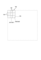
- FIG. 1 is a schematic diagram showing an example of a configuration of a microscope according to a first embodiment
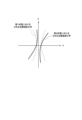
- FIG. FIG. 5 is a diagram showing an example in which the Z-direction intensity profile of the three-dimensional point spread intensity distribution differs between the optical system in the first state and the optical system in the second state according to the first embodiment
- FIG. 4 is a diagram schematically showing the relationship between a focal plane, a sample plane, a first plane, a second plane, and an estimated sample plane according to the first embodiment
- FIG. 4 is a diagram showing an example of a plurality of images generated by the generator of the first embodiment
- FIG. 4 is a diagram showing an example of a two-dimensional point spread intensity distribution on a first surface and a two-dimensional point spread intensity distribution on a second surface in the optical system in the first state and the optical system in the second state of the first embodiment; 4 is a flow chart showing the flow of an image processing method according to the first embodiment; It is a figure which shows an example of the estimation image based on the structure estimated by the estimation part of 1st Embodiment. It is a schematic diagram showing an example of a configuration of a microscope according to a second embodiment.
- FIG. 10 is a diagram schematically showing the relationship between the focal plane, the sample plane, the first plane, the second plane, and the estimated sample plane according to the second embodiment; FIG.
- FIG. 11 is a schematic diagram showing an example of the configuration of a microscope according to a third embodiment; It is a figure which shows the structure of the detector based on 3rd Embodiment.
- FIG. 11 is a diagram schematically showing the relationship between the focal plane, the sample plane, the first plane, the second plane, and the estimated sample plane according to the third embodiment; It is a schematic diagram showing an example of a configuration of a microscope according to a fourth embodiment.
- FIG. 11 is a diagram showing the outline of the XZ cross section of the three-dimensional point spread intensity distribution in the first state and the outline of the XZ cross section of the three-dimensional point spread intensity distribution in the second state according to the fourth embodiment;
- FIG. 11 is a diagram showing the outline of the XZ cross section of the three-dimensional point spread intensity distribution in the first state and the outline of the XZ cross section of the three-dimensional point spread intensity distribution in the second state according to the fourth embodiment;
- FIG. 11 is a diagram showing an example of a two-dimensional point spread intensity distribution on a first surface and a two-dimensional point spread intensity distribution on a second surface in the optical system in the first state and the optical system in the second state of the fourth embodiment;
- FIG. 11 is a schematic diagram showing an example of the configuration of a microscope according to a fifth embodiment;
- FIG. 11 is a diagram showing an example of a two-dimensional point spread intensity distribution on a first surface and a two-dimensional point spread intensity distribution on a second surface in the optical system in the first state and the optical system in the second state according to the fifth embodiment;
- FIG. 11 is a schematic diagram showing an example of the configuration of a microscope according to a sixth embodiment;
- FIG. 12 is a diagram showing an example of a two-dimensional point spread intensity distribution on the first surface and a two-dimensional point spread intensity distribution on the second surface in the optical system in the first state and the optical system in the second state of the sixth embodiment;
- FIG. 11 is a schematic diagram showing an example of the configuration of a microscope according to a seventh embodiment;
- FIG. 12 is a diagram showing an example of a two-dimensional point spread intensity distribution on the first surface and a two-dimensional point spread intensity distribution on the second surface in the optical system in the first state and the optical system in the second state of the seventh embodiment;
- FIG. 21 is a schematic diagram showing an example of the configuration of a microscope according to an eighth embodiment;
- FIG. 21 is a schematic diagram showing an example of the configuration of a microscope according to a ninth embodiment;
- FIG. 20 is a diagram showing an example of a two-dimensional point spread intensity distribution on the first surface and a two-dimensional point spread intensity distribution on the second surface in the optical system in the first state and the optical system in the second state of the ninth embodiment
- FIG. 22 is a schematic diagram showing an example of the configuration of a microscope according to the tenth embodiment
- FIG. 20 is a diagram showing an example of a two-dimensional point spread intensity distribution on the first surface and a two-dimensional point spread intensity distribution on the second surface in the optical system in the first state and the optical system in the second state of the tenth embodiment
- FIG. 21 is a schematic diagram showing an example of the configuration of a microscope according to an eleventh embodiment
- FIG. 20 is a diagram showing examples of two-dimensional point spread amplitude distributions on the first surface and two-dimensional point spread amplitude distributions on the second surface in the optical system in the first state and the optical system in the second state of the eleventh embodiment;
- FIG. 21 is a schematic diagram showing an example of the configuration of a microscope according to a twelfth embodiment;
- FIG. 22 is a diagram showing examples of a plurality of images generated by a generation unit according to the twelfth embodiment;
- FIG. 22 is a diagram showing an example of an estimated image based on the structure estimated by the estimation unit of the twelfth embodiment;
- FIG. 1 is a schematic diagram showing an example of the configuration of a microscope according to the first embodiment.
- the microscope 1A will be described as a confocal microscope.
- the microscope 1A includes a microscope body 10A and an image processing device 100A.
- the microscope main body 10A includes a light source 11, an optical system 12, a scanning control section 13, and a detector 15A.
- the light source 11 emits illumination light L1 such as a laser.
- the light source 11 may be a monochromatic (single wavelength) light source or a polychromatic (multiple wavelengths) light source.
- the light source 11 may be either a laser that emits continuous wave light or a laser that emits pulsed light. Also, the light source 11 may be an LED or a lamp instead of a laser.
- a substance that emits fluorescence is used as the sample 8 , it is preferable to select a wavelength that excites the fluorescent substance contained in the sample 8 as the wavelength of the light source 11 .
- a wavelength for multiphoton excitation of the fluorescent substance contained in the sample 8 may be selected as the wavelength of the light source 11 .
- the light source 11 may be replaceably (attachable or detachable) provided in the microscope main body 10A.
- the light source 11 may be externally attached to the microscope main body 10A during observation with the microscope main body 10A.
- illumination light L1 may enter the microscope main body 10A from a light source 11 outside the microscope main body 10A via an existing optical member such as an optical fiber.
- the optical system 12 irradiates the sample 8 with the illumination light L1 from the light source 11 and guides the detection light L2 from the sample 8 to the detector 15A.
- the optical system 12 includes a collimator lens 120, an objective lens 121, a pupil projection lens 122, a lens 123, a deflection section 124, an optical path separation element 125, a condenser lens 126, and the like.
- the collimator lens 120 converts the illumination light L1 emitted from the light source 11 such as a laser into substantially parallel light.
- the optical path separation element 125 is composed of a dichroic mirror or the like. The optical path separation element 125 causes the illumination light L1 that has passed through the collimator lens 120 to enter the deflection section 124 .
- the deflection unit 124 causes the incident illumination light L1 to enter the objective lens 121 through the pupil projection lens 122 and the lens 123 .
- the deflection unit 124 is provided with an X-direction deflection mirror and a Y-direction deflection mirror.
- the deflection unit 124 is arranged substantially conjugate with the pupil position of the objective lens 121 via the objective lens 121 , the lens 123 and the pupil projection lens 122 with respect to the sample 8 .
- the objective lens 121 irradiates the sample 8 held on the stage 2 with the incident illumination light L1.
- the objective lens 121 forms an illumination area 14 on the sample 8 in which the illumination light L1 is condensed to a size about the resolution limit of the objective lens 121 .
- the illumination area 14 on the sample 8 will be the illumination area 14 with light of the single wavelength.
- the illumination area 14 on the sample 8 will be the illumination area 14 including multiple wavelengths.
- the scanning control unit 13 controls the X-direction deflection mirror and the Y-direction deflection mirror of the deflection unit 124 to swing in a predetermined direction, so that the illumination area 14 is aligned with the plane perpendicular to the optical axis direction of the illumination light L1 on the sample 8. Scan along.
- the scanning control unit 13 moves the stage 2 holding the sample 8 along a plane perpendicular to the optical axis direction of the illumination light L1, thereby relatively scanning the illumination area 14 and the sample 8 on the stage 2.
- both scanning by the deflection unit 124 and scanning by the stage 2 may be performed.
- the detection light L2 is refracted by the objective lens 121, passes through the lens 123 and the pupil projection lens 122, and reaches the deflection section .
- the detection light L2 is returned (descanned) along substantially the same optical path as the illumination light L1 by being reflected by the deflector 124 and reaches the optical path separation element 125 .
- the detection light L2 passes through the optical path separation element 125 and the condenser lens 126 and enters the detector 15A.
- the optical system that guides the illumination light L1 emitted from the light source 11 to the sample 8 is the illumination optical system. That is, each optical member (optical path separating element 125, deflection unit 124, pupil projection lens 122, lens 123, objective lens 121, etc.) arranged on the optical path from the optical path separating element 125 to the sample 8 constitutes an illumination optical system. do.
- An optical system that guides the light emitted from the sample 8 to the detector 15A is a detection optical system.
- each optical member (objective lens 121, pupil projection lens 122, lens 123, deflection unit 124, optical path separation element 125, condenser lens 126, etc.) arranged on the optical path from the sample 8 to the detector 15A detects Configure the optical system.
- the detector 15A is arranged at a position that is conjugate with the illumination area 14 on the sample 8 via the detection optical system, that is, at a position that forms an image with the illumination area 14 on the sample 8 via the detection optical system.
- a fluorescence image 15m of the sample 8 excited in the illumination region 14 is formed as an image of the illumination region 14 on the light receiving surface of the detector 15A.
- the detector 15A detects an image 15m formed on the light receiving surface of the detector 15A.
- the detector 15A is a point detector 151 whose light receiving surface is sufficiently smaller than the fluorescence image 15m of the sample 8.
- the point detector 151 includes a photoelectric conversion element (not shown) made of semiconductor or the like.
- a photoelectric conversion element (not shown) of the detector 15A outputs a signal (electrical signal) corresponding to the detected amount of light to the image processing device 100A.
- the detector 15A can be moved between a plurality of positions by the detector control section 16 within a plane orthogonal to the optical axis direction of the detection light L2.
- the detector 15A is movable between any first position G1 and second position G2 within a plane orthogonal to the optical axis direction of the detection light L2. ing.
- the movement of the detector 15A is controlled by the detector controller 16 within a plane orthogonal to the optical axis direction of the detection light L2.
- the detector 15A moves on a plane orthogonal to the optical axis direction, and detects the light amount of the image 15m at each of a plurality of positions on the plane orthogonal to the optical axis direction.
- FIG. 2 is a diagram showing an example in which the Z-direction intensity profile of the three-dimensional point spread intensity distribution differs between the optical system in the first state and the optical system in the second state according to the embodiment.
- Detector 15A changes its position relative to light source 11 when its position on the plane perpendicular to the optical axis direction changes.
- the three-dimensional point spread intensity distribution (3D-PSF) via the optical system 12 changes. That is, as shown in FIG. 2, the first state A1 in which the detector 15A is positioned at an arbitrary first position G1 is different from the first position G1 in the plane orthogonal to the optical axis direction.
- the three-dimensional point image intensity distribution via the optical system 12 is different from the second state A2 located at the arbitrary second position G2.
- the three-dimensional point image intensity distribution is a function that quantitatively expresses the intensity distribution of the detection light L2 emitted from a point object existing on the sample 8 and detected by the detector 15A.
- the system and the optical system in the second state are determined by the relative relationships with the light source 11, the optical system 12, and the detector 15A, respectively. Therefore, the optical system in the first state and the optical system in the second state include the light source 11, the optical system 12, and the detector 15A. It should be noted that the same applies when the configuration of the optical system 12 and the detector are different as in other embodiments.
- the image processing device 100A generates an image of the sample 8 based on the signal from the detector 15A and processes the image.
- the image processing apparatus 100A is composed of a computer such as a personal computer.
- the image processing apparatus 100A includes hardware such as a CPU and memory.
- the image processing apparatus 100A functionally has the following configuration by executing predetermined processing in cooperation with a CPU, memory, etc., and an image processing program stored in the memory or storage device.
- the image processing device 100A functionally includes a signal receiving section 101, a generating section 102, and an estimating section 103.
- the signal receiving section 101 receives a signal corresponding to the amount of light of the image 15m output from the detector 15A.
- the generator 102 generates a two-dimensional image of the sample 8 on the focal plane F based on the signal corresponding to the light intensity from the detector 15A and the relative positional relationship between the illumination region 14 and the sample 8 when the light intensity signal is detected. An image (two-dimensional image data) is generated.
- FIG. 3 is a diagram schematically showing the relationship between the focal plane, the sample plane, the first plane, the second plane, and the estimated sample plane according to the embodiment.
- the focal plane F in the optical system in each state is a plane defined from the three-dimensional point spread intensity distribution of the optical system in each state.
- the position of the focal plane F in the optical system in each state can change in the optical axis direction (Z direction) depending on the position of the detector 15A with respect to the light source 11.
- the position of the detector 15A in the first state A1 (first position G1) is different from the position of the detector 15A in the second state A2 (second position G2). Therefore, the three-dimensional point spread intensity distribution through the optical system differs between the first state A1 and the second state A2.
- the position in the optical axis direction (Z direction) can be different from the second focal plane Fb, which is the focal plane in A2.
- the positions of the first focal plane Fa and the second focal plane Fb match in the optical axis direction (Z direction).
- the first focal plane Fa and the second focal plane Fb are matched if they are equal to or less than the size of the image intensity distribution.
- the focal plane F is, for example, the central position of the Gaussian when three-dimensional Gaussian fitting is performed to obtain an approximate function of the three-dimensional point spread intensity distribution of the optical system 12 in each corresponding state. It is an existing plane (XY plane).
- the focal plane F intersects the plane (XY plane) at the position where the maximum brightness of the three-dimensional point spread intensity distribution of the optical system in each corresponding state exists in the Z direction, or the axial direction (Z direction).
- the plane (XY plane) where the maximum value of the integrated value of the three-dimensional point spread distribution of the optical system in each corresponding state exists on the corresponding plane may be defined.
- the focal plane F is, for example, the XY plane in the Z coordinate where the central position of Gaussian exists when the three-dimensional point spread intensity distribution of the optical system in a certain state is subjected to 3D Gaussian fitting.
- the detector 15A detects the image 15m at multiple positions in a plane orthogonal to the optical axis direction. Therefore, the generation unit 102 generates a plurality of images G of the sample 8 based on the amount of light detected by the detector 15A at a plurality of positions in a plane perpendicular to the optical axis direction. As shown in FIG. 3, in the generation unit 102, the surface of the sample 8 (this is called the first sample A first image Ga of the surface Sa) is generated. In the generation unit 102, based on the amount of light detected by the detector 15A in the second state A2, the surface of the sample 8 (referred to as the second sample surface Sb) at the position corresponding to the second focal plane Fb in the Z direction. 2 images Gb are generated.
- the focal planes F of the optical system in all states for acquiring the images G of the plurality of samples generated by the generation unit 102 are at the same position or close to each other in the Z direction.
- the distribution of the Z coordinates of all focal planes F falls within a range of 10% or less of the Z resolution (half width of the Z profile of the three-dimensional point spread intensity distribution) of each optical system in all states. In this case, it is expressed that a plurality of focal planes F are substantially coincident.
- the generation unit 102 generates all focal planes based on the signal corresponding to the light intensity from the detector 15A and the relative positional relationship between the illumination region 14 and the sample 8 when the light intensity signal is detected.
- a two-dimensional image G of the sample 8 at F is generated.
- a two-dimensional image G is represented by the following formula (1).
- I (x, y, z) is the image G
- h (x, y, z) is the three-dimensional point spread intensity distribution in the optical system 12
- s (x, y, z) is the fluorescence in the sample 8. molecular distribution.
- FIG. 4 is a diagram illustrating an example of a plurality of images generated by the generation unit;
- the image group of the plurality of images G generated by the generation unit 102 is the first focal plane Fa based on the signal from the detector 15A via the optical system 12 in the first state A1.
- the second focal plane Fb substantially coincides with the first focal plane Fa in the optical axis direction (Z direction). 2 images Gb.
- the first image Ga is an observation image obtained with the first focal plane Fa aligned with the first sample plane Sa of the sample 8 .
- the second image Gb is an observation image obtained with the second focal plane Fb aligned with the second sample plane Sb of the sample 8 .
- m1 to m3 are objects in the sample 8.
- Data of a plurality of images G generated by the generating unit 102 are input to the estimating unit 103 .
- the detector 15A is positioned at a plurality of positions in a plane orthogonal to the optical axis direction to detect the amount of light of the image 15m
- the plurality of images G are obtained when the focal plane F of the optical system in each state corresponds to each sample surface.
- the photograph was taken in a state suitable for S.
- the positions (Z coordinates) in the Z direction of the focal planes F of the optical systems in all the states for acquiring a plurality of images G approximately match each other based on the above definition.
- the estimation unit 103 sets an estimated sample surface for estimating the structure of the sample 8.
- the estimation unit 103 generates a first estimated sample surface Q1 at a position corresponding to the first surface P1 in the Z direction and a second estimated sample surface Q2 at a position corresponding to the second surface P2 in the Z direction. to deduce the structure of sample 8, respectively.
- the first plane P1 is determined to substantially coincide with the focal plane F.
- the first plane P1 has a Z coordinate of The first plane P1 is selected so that it is less than or equal to Zmax and greater than or equal to Zmin.
- the estimating unit 103 estimates the structure of each of the plurality of estimated sample surfaces along the optical axis direction (Z direction) of the optical system 12 based on the plurality of images G generated by the generating unit 102, and calculates the structure of the first estimated sample.
- An estimated image Ie of the surface Q1 is output.
- the second plane P2 is set as a non-focal plane. That is, the second plane P2 is set outside the z-coordinate range (Zmin to Zmax) of the focal plane F.
- the estimating unit 103 calculates the two-dimensional point spread intensity distribution of the first plane P1 and the second plane P2 in the three-dimensional point spread intensity distribution of each of the optical systems in all states for acquiring the multiple images G, or stored in advance.
- the point spread h Let x, y, z1) be the two-dimensional point spread intensity distribution H1 on the first plane P1.
- FIG. 5 shows the two-dimensional point spread intensity distribution of the first surface P1 and the two-dimensional spot spread intensity distribution of the second surface P2 in the optical system in the first state of the embodiment, and the first It is a figure which shows the example of the two-dimensional point spread intensity distribution of the surface P1, and the two-dimensional point spread intensity distribution of the 2nd surface P2.
- FIG. 5 shows the present embodiment, as shown in FIG.
- the two-dimensional point spread H1a of the first plane P1 and the second plane P2 is a two-dimensional point on the first surface P1 in the second three-dimensional point spread based on the optical system in the second state A2 different from the first state A1.
- the second relative relationship between the image intensity distribution H1b and the two-dimensional point spread intensity distribution H2b on the second surface P2 is different.
- the estimating unit 103 uses at least one set of images G to estimate the structure of each of a plurality of surfaces including the first estimated sample surface Q1 on the sample 8 along the optical axis direction (Z direction) of the optical system 12.
- the estimating unit 103 utilizes the fact that the two-dimensional point spread intensity distributions have different relative relationships, and uses at least one pair of images G to estimate the first estimated sample plane Q1 and the second estimated sample plane Q2.
- the structure of sample 8 in is deduced separately. If there is no difference in the relative relationship between the two-dimensional point spread intensity distributions, the structure of the sample 8 on the first estimated sample surface Q1 and the second estimated sample surface Q2 cannot be correctly estimated.
- the estimating unit 103 calculates the structure of the sample 8 on the first estimated sample plane Q1 and the second estimated sample plane Q2 by combining the two-dimensional point spread intensity distribution on the first plane P1 and the two-dimensional point spread intensity on the second plane P2. It can be estimated based on the difference in relative intensity of the distributions.
- the optical system in the first state A1 the first relative intensity between the two-dimensional point spread intensity distribution on the first surface P1 and the two-dimensional point spread intensity distribution on the second surface P2, and the optical system in the second state A2 , there is preferably a predetermined difference between the second relative intensity of the two-dimensional point spread intensity distribution on the first plane P1 and the second relative intensity distribution of the two-dimensional spot spread on the second plane P2.
- I f 1 be the sum of the luminance of the two-dimensional point spread H1a on the first surface P1 of the optical system in the first state A1, and the luminance of the two-dimensional point spread H1b on the second surface P2 of the optical system in the first state A1.
- I df be the total sum
- I f 2 be the luminance sum of the two-dimensional point spread H1b on the first surface P1 of the optical system in the second state A2
- I f 2 be the sum of the second surfaces P2 of the optical system in the second state A2.
- s is a P-dimensional vector representing a three-dimensional distribution of fluorescent molecules
- (x n , y n ) are the coordinates of the illumination area 14 of the illumination light L1
- (x p , y p , z p ) are the coordinates of the sample space.
- hm represents the three-dimensional point spread intensity distribution of the optical system when the detector 15A is placed at the m-th position (state).
- the estimation unit 103 estimates the distribution of fluorescent molecules in the sample 8 by minimizing the error function F(s) represented by the following formula (6).
- the estimation unit 103 performs processing to find ⁇ that minimizes the error function represented by the above equation (7). If the gradient method is used in the estimator 103, the following equation (8) is obtained at the i-th iteration.
- d i represents the gradient of the error function F(s) with respect to ⁇
- the estimation unit 103 estimates the distribution of fluorescent molecules on the first estimated sample surface Q1 and the second estimated sample surface Q2.
- the estimation unit 103 separately estimates the structure of the sample 8 on the first estimated sample plane Q1 and the second estimated sample plane Q2. direction) may be set at different positions.
- the second estimated sample surface Q2 may be set on the + side and the - side of the optical axis direction (Z direction) with respect to the first estimated sample surface Q1.
- each process executed by the image processing device 100A of the microscope main body 10A is executed by the image processing device 100A based on a program pre-stored in the image processing device 100A.
- This program may be provided by being recorded on a computer-readable storage medium (eg, non-transitory tangible media).
- FIG. 6 is a flow chart showing the flow of the image processing method according to the embodiment.
- the sample 8 set on the stage 2 is irradiated with the illumination light L1 from the light source 11 .
- Illumination light L1 emitted from the light source 11 passes through a collimator lens 120, an optical path separation element 125, a deflector 124, a pupil projection lens 122, an imaging lens 123, and an objective lens 121, and reaches a sample held on the stage 2. 8 are illuminated. Thereby, an illumination area 14 in which the illumination light L1 is condensed by the objective lens 121 is formed on the sample 8.
- the scanning control unit 13 controls the oscillation of the deflection unit 124 to two-dimensionally scan the illumination region 14 on the sample 8 in the XY directions. While the illumination region 14 is two-dimensionally scanned on the sample 8 in the XY directions, the relative positional relationship in the Z direction between the sample 8 and the objective lens 121 is not changed (maintained and fixed), and the illumination region 14 is located on the sample. 8 is scanned in the predetermined Z plane.
- Light (detection light) L2 emitted from the sample 8 by irradiation of the illumination area passes through the objective lens 121, the imaging lens 123, the pupil projection lens 122, the deflection unit 124, the optical path separation element 125, and the condenser lens 126, Incident on the detector 15A.
- step S12 the detector control unit 16 moves the detector 15A to a plurality of positions within the XY plane, and at each position, the detector 15A controls the fluorescence of the sample 8 formed on the light receiving surface of the detector 15A. is detected.
- a photoelectric conversion element (not shown) of the detector 15A outputs a signal (electrical signal) corresponding to the amount of received light to the image processing device 100A. Even when the detector 15A is moved to a plurality of positions in the XY plane, the relative positional relationship in the Z direction between the sample 8 and the objective lens 121 is not changed (maintained and fixed), and the illumination area 14 is the same as that of the sample 8.
- a predetermined Z plane is scanned.
- step S13 the image processing device 100A generates an image G of the sample 8 based on the signal from the detector 15A, and processes the generated image G.
- a signal receiving unit 101 of the image processing apparatus 100A receives a signal output from the detector 15A corresponding to the light amount of the fluorescence image 15m of the sample 8 received by the photoelectric conversion element (not shown).
- the generator 102 generates a two-dimensional image of the sample 8 on the focal plane F based on the signal corresponding to the light intensity from the detector 15A and the relative positional relationship between the illumination region 14 and the sample 8 when the light intensity signal is detected.
- the generator 102 generates a plurality of images G (image group) based on the amount of light detected by the detector 15A at a plurality of positions within the XY plane.
- An image G is an image acquired without changing the relative positional relationship in the Z direction between the sample 8 and the objective lens 121 (optical system 12).
- the image group of the plurality of images G generated by the generation unit 102 is the first focal plane based on the signal from the detector 15A via the optical system 12 in the first state A1 in which the detector 15A is positioned at the first position G1.
- the first image Ga of Fa and the first focal plane Fa and the optical axis direction and a second image Gb of a second focal plane Fb substantially coincident in the Z direction).
- the first image Ga is obtained with the first focal plane Fa aligned with the first sample plane Sa of the sample 8 .
- the second image Gb is obtained with the second focal plane Fb aligned with the second sample plane Sb of the sample 8 .
- the estimating unit 103 estimates the structure of each of the plurality of surfaces of the sample 8 along the optical axis direction (Z direction) of the optical system based on the group of images generated by the generating unit 102. output an estimated image Ie based on the structure obtained.
- the estimation unit 103 receives data of a plurality of images G (image group) generated by the generation unit 102 .
- the estimating unit 103 calculates or stores in advance the two-dimensional point spread intensity distributions of the first plane P1 and the second plane P2 in the three-dimensional point spread distribution based on the optical system.
- the first plane P1 is determined to substantially coincide with the focal plane F.
- the second surface P2 is a non-focal surface and differs from the first surface P1 in the optical axis direction (Z direction) of the optical system.
- a first relative relationship between the two-dimensional point spread intensity distribution of the first surface P1 and the two-dimensional point spread intensity distribution of the second surface P2 in the first three-dimensional point spread intensity distribution based on the optical system in the first state A1 is the two-dimensional point image intensity distribution of the first surface P1 and the two-dimensional point image of the second surface P2 in the second three-dimensional point image intensity distribution based on the optical system in the second state A2 different from the first state A1 Different for a second relative relationship with the intensity distribution.
- the estimating unit 103 uses at least one set of images G to estimate the structure of each of a plurality of surfaces including the first estimated sample surface Q1 on the sample 8 along the optical axis direction (Z direction) of the optical system.
- the sample surface S corresponding to the first surface P1 is defined as a first estimated sample surface Q1
- the sample surface S corresponding to the second surface P2 is defined as a second estimated sample surface Q2.
- the estimating unit 103 calculates the structure of the sample 8 on the first estimated sample plane Q1 and the second estimated sample plane Q2 by combining the two-dimensional point spread intensity distribution on the first plane P1 and the two-dimensional point spread intensity on the second plane P2. Estimate based on relative intensity with distribution.
- the estimation unit 103 estimates the structure of each of a plurality of estimated sample surfaces (estimated sample surfaces) and outputs an estimated image Ie based on the estimated structure. For example, the estimated image on the first estimated sample plane Q1 and the estimated image on the second estimated sample plane Q2 are respectively weighted differently, and the summed (integrated) image is defined as Ie.
- w k is a weight for the estimated image at the k-th estimated sample plane Q k and can take any real value.
- the estimated image Ie obtained in this way is the first image Ga and the second image Ga
- the structure of the non-focal plane is relatively reduced compared to Gb, and it can be said that the resolution in the optical axis direction (Z direction) is improved.
- the weight it is possible to change the sectioning ability of the estimated image Ie. Further, consider a modified three-dimensional point spread intensity distribution given by the following equation, in which different weights are assigned to z of the three-dimensional point spread intensity distribution.
- wz is the weight for each z of the three-dimensional point spread intensity distribution, and can take any positive real value other than 0.
- an estimated image Ie equivalent to the above is obtained by integrating the estimated images on each estimated sample plane with a weight of 1.
- the flowchart showing the flow of the image processing method shown in FIG. 6 is also applied to other embodiments.
- other embodiments differ in the microscope main body (optical system configuration, type of detector) and image processing device (as a result, the optical system in the first state and the optical system in the second state are different)
- the content of each step in the flowchart can be applied by replacing the configuration and function of the microscope main body and the image processing apparatus of each embodiment.
- FIG. 7 is a diagram showing an example of an estimated image Ie based on the structure estimated by the estimation unit of the first embodiment.
- the estimating unit 103 analyzes the plurality of first images Ga and second images Gb (see FIG. 4) acquired in the first state A1 and the second state A2 to obtain the first estimated sample surface
- the objects m2 and m3 that do not exist on Q1 are removed or reduced, and an estimated image Ie in which the object m1 that exists on the first estimated sample plane Q1 is emphasized is output.
- the detector 15A composed of the point detector 151 performs detection at a plurality of positions, thereby obtaining the first image based on the signal from the point detector 151 in the first state A1.
- the first estimated sample in the sample 8 Estimate the structure of each of a plurality of planes including the plane Q1. Therefore, the sample structure can be estimated based on more image information obtained by the point detector 151 performing detection at a plurality of positions.
- the object existing on the first estimated sample plane Q1 can be estimated with higher accuracy, and an estimated image Ie with improved Z resolution and sectioning performance can be obtained.
- the Z resolution refers to the half width of the Z profile at the (x, y) coordinates where the peak intensity of the three-dimensional point spread is present.
- the sectioning ability indicates the half width of the Z profile of the integrated values in the xy plane of the three-dimensional point image.
- FIG. 8 is a schematic diagram showing an example of the configuration of a microscope according to the second embodiment.
- the same reference numerals may be given to the same configurations as in the above-described embodiment, and the description thereof may be omitted or simplified.
- the microscope 1B includes a microscope body 10B and an image processing device 100B.
- the microscope main body 10B includes a light source 11, an optical system 12, a scanning control section 13, and a detector 15B.
- the optical system 12 of the microscope body 10B irradiates the sample 8 with the illumination light L1 from the light source 11 and guides the detection light L2 from the sample 8 to the detector 15B.
- the detector 15B includes a plurality of point detectors 152.
- the multiple point detectors 152 are arranged in a plane perpendicular to the optical axis direction of the detection light L2.
- the plurality of point detectors 152 are integrally attached to a base member (not shown) or the like.
- the number of installed point detectors 152, arrangement, etc. are not limited at all.
- the plurality of point detectors 152 may be linearly arranged in one direction along a plane orthogonal to the optical axis direction of the detection light L2.
- the plurality of point detectors 152 may be discretely arranged within a plane orthogonal to the optical axis direction of the detection light L2. In FIG. 8, for example, three point detectors 152 are arranged along the vertical direction of the page of FIG.
- Each point detector 152 includes a photoelectric conversion element (not shown) made of semiconductor or the like.
- a photoelectric conversion element (not shown) of each point detector 152 outputs a signal (electrical signal) corresponding to the amount of received light to the image processing device 100B.
- the detector 15B detects the light amount of the image 15m at each of the plurality of point detectors 152 at a plurality of positions in a plane orthogonal to the optical axis direction.
- a plurality of point detectors 152 constituting the detector 15B are different in position on a plane orthogonal to the optical axis direction. Therefore, the relative position with respect to the light source 11 changes between the plurality of point detectors 152 .
- the three-dimensional point spread intensity distribution (3D-PSF) through the optical system 12 changes as shown in FIG.
- FIG. 8 focusing on two point detectors 152 among the plurality of point detectors 152, the detector 152 in the first state A11 located at the first position G11 and the detector 152 in the first state A11 are perpendicular to the optical axis direction.
- the three-dimensional point image intensity distribution via the optical system 12 is different from the point detector 152 in the second state A12 located at an arbitrary second position G12 different from the first position G11 in the plane.
- the image processing device 100B generates multiple images of the sample 8 based on the signals from the multiple point detectors 152 of the detector 15B, and processes these images.
- the image processing apparatus 100B includes a signal receiving section 101, a generating section 102, and an estimating section 103, and each function is as described in the first embodiment, and is also applied to the present embodiment.
- the position of the focal plane F in the optical system in each state can change in the optical axis direction (Z direction) depending on the positions of the plurality of point detectors 152 with respect to the light source 11 .
- the detector 15B in the first state A11 located at the first position G11 and the detector 15B in the second state A12 located at the second position G12 are three-dimensional points via the optical system 12. The image intensity distribution is different.
- the first focal plane Fa which is the focal plane in the first state A11
- the second focal plane Fb which is the focal plane in the second state A12
- Z direction optical axis direction
- the detector 15B since the detector 15B includes a plurality of point detectors 152, it is possible to acquire a large number of images at the same time. Therefore, the sample structure can be estimated based on more image information obtained by the multiple point detectors 152 . As a result, the object existing on the first estimated sample surface Q1 can be more easily estimated, and an estimated image Ie with improved Z-resolution and sectioning performance can be obtained. In addition, since the detector 15B includes a plurality of point detectors 152, the amount of light can be detected at a plurality of positions at the same time, so that more rapid processing can be performed.
- FIG. 10 is a schematic diagram showing an example of the configuration of a microscope according to the third embodiment.
- the same reference numerals may be given to the same configurations as in the above-described embodiment, and the description thereof may be omitted or simplified.
- the microscope 1C includes a microscope body 10C and an image processing device 100C. 10 C of microscope main bodies are provided with the light source 11, the optical system 12, the scanning control part 13, and the detector 15C.
- the optical system 12 of the microscope main body 10C irradiates the sample 8 with the illumination light L1 from the light source 11 and guides the detection light L2 from the sample 8 to the detector 15C.
- FIG. 11 is a diagram showing the configuration of a detector according to the third embodiment.
- the detector 15C detects the light of the image 15m formed on the light receiving surface of the detector 15C.
- the detector 15C is a so-called two-dimensional detector (2D detector), and is configured by arranging a plurality of detectors 153 two-dimensionally.
- the plurality of detectors 153 are arranged in a first direction along a plane orthogonal to the optical axis direction (horizontal direction in FIG. 11) and in a second direction along a plane orthogonal to the optical axis direction and intersecting the first direction. A plurality of them are arranged in each direction (vertical direction on the paper surface of FIG. 11).
- each detection unit 153 is a pixel that detects light and has a light-receiving surface sufficiently smaller than the fluorescence image 15m of the sample 8 .
- the detection unit 153 includes a photoelectric conversion element (not shown) made of semiconductor or the like.
- the light receiving surface of detector 15C receives the light of image 15m.
- Each of the plurality of detection units 153 forming the detector 15C outputs a signal (electrical signal) corresponding to the amount of received light to the image processing device 100C.
- FIG. 12 is a diagram schematically showing the relationship between the focal plane, the sample plane, the first plane, the second plane, and the estimated sample plane according to the third embodiment. If the positions on the plane orthogonal to the optical axis direction are different among the plurality of detecting portions 153 of the detector 15C, the relative positions with respect to the light source 11 are changed. When the relative position of the detector 15C detector 153 with respect to the light source 11 changes, the three-dimensional point spread intensity distribution (3D-PSF) through the optical system 12 changes as shown in FIG. That is, as shown in FIG.
- 3D-PSF three-dimensional point spread intensity distribution
- the optical system in the first state A21 including the light source 11, the optical system 12, and the detection unit 153 positioned at the first position G21 is different from that of the optical system in the second state A22 including the light source 11, the optical system 12, and the detection unit 153 positioned at the second position G22.
- the image processing device 100C generates multiple images of the sample 8 based on the signals from the multiple detection units 153 of the detector 15C, and processes these images.
- the image processing apparatus 100C includes a signal receiving unit 101, a generating unit 102, and an estimating unit 103, and each function is also applied in this embodiment as described in the first embodiment.
- the focal plane F in the optical system in each state is a plane defined from the three-dimensional point spread intensity distribution of the optical system in each state.
- the description in the first embodiment also applies to this embodiment. Therefore, all focal planes are substantially coincident.
- the detector 15C includes a plurality of detectors 153 arranged two-dimensionally, so that the amount of light can be detected at a plurality of positions at the same time. , can be processed more quickly.
- the plurality of detectors 153 arranged two-dimensionally can obtain more image information in the same scanning time. A more accurate estimated image Ie is obtained.
- FIG. 13 is a schematic diagram showing an example of the configuration of a microscope according to the fourth embodiment.
- the same reference numerals may be given to the same configurations as in the above-described embodiment, and the description thereof may be omitted or simplified.
- the microscope 1D includes a microscope body 10D and an image processing device 100D.
- a microscope body 10D includes a light source 11, an optical system 12, a scanning control section 13, and a detector 15D.
- the detector 15D detects the detection light L2 from the sample 8.
- the detector 15D comprises a point detector 154.
- the point detector 154 includes a photoelectric conversion element (not shown) made of semiconductor or the like. Each photoelectric conversion element (not shown) of the point detector 154 outputs a signal (electrical signal) corresponding to the amount of received light to the image processing device 100D.
- the point detector 154 is fixedly provided.
- the optical system 12 is provided with an optical element 17D.
- the optical element 17D switches the optical system 12 between the first state A31 and the second state A32.
- the optical element 17D is provided so as to move back and forth with respect to the optical path of the detection light L2.
- the optical element 17D is configured to be switchable between a first state A31 in which the optical element 17D is positioned outside the optical path of the detection light L2 and a second state A32 in which the optical element 17D enters the optical path of the detection light L2.
- a glass parallel plate 171 is provided as the optical element 17D.
- the glass parallel plate 171 is arranged, for example, between the optical path separation element 125 and the condenser lens 126 . In the second state A32 in which the parallel glass plate 171 enters the optical path of the detection light L2, the detection light L2 shifts in the direction intersecting the optical axis direction (Z direction).
- FIG. 14 is a diagram showing the outline of the XZ cross section of the three-dimensional point spread intensity distribution in the first state and the outline of the XZ cross section of the three-dimensional point spread intensity distribution in the second state according to the fourth embodiment.
- the detection light L2 shifts in a plane orthogonal to the optical axis direction (Z direction), thereby producing a three-dimensional point spread intensity distribution (3D-PSF ) changes.
- a second state A32 in which the glass parallel plate 171 is positioned on the optical path of the detection light L2.
- the three-dimensional point image intensity distribution through the optical system 12 is different, and the three-dimensional point image intensity distribution in the second state A32 is tilted with respect to the three-dimensional point image intensity distribution in the first state A31.
- the image processing device 100D generates an image of the sample 8 based on the signal from the point detector 154 of the detector 15D and processes the image.
- the generator 102 generates an image of the focal plane F of the optical system based on the signal from the point detector 154 .
- the generation unit 102 causes the point detector 154 to An image G of the sample 8 is generated based on the detected amount of light.
- the generation unit 102 generates a first image of the surface of the sample 8 (first sample surface Sa) at a position corresponding to the first focal plane Fa in the Z direction based on the amount of light detected by the detector 15D in the first state A31. Generate Ga.
- the generation unit 102 generates a second image of the surface of the sample 8 (second sample surface Sb) at a position corresponding to the second focal plane Fb in the Z direction based on the amount of light detected by the detector 15D in the second state A32.
- FIG. 15 shows the two-dimensional point spread intensity distribution on the first surface and the two-dimensional spot spread intensity distribution on the second surface in each of the optical system in the first state and the optical system in the second state of the fourth embodiment. It is a diagram. As shown in FIG. 15, in the first three-dimensional point image intensity distribution based on the optical system in the first state A31, a two-dimensional point image intensity distribution H31a on the first surface P1 and a two-dimensional point image on the second surface P2 The first relative relationship with the intensity distribution H32a is the two-dimensional point spread intensity distribution H31b on the first surface P1 in the second three-dimensional point spread intensity distribution based on the optical system in the second state A32 different from the first state A31. , with respect to a second relative relationship with the two-dimensional point spread H32b on the second surface P2.
- the estimating unit 103 calculates the structure of the sample 8 on the first estimated sample plane Q1 and the second estimated sample plane Q2 by the two-dimensional point spread intensity distribution on the first plane P1 and the two-dimensional point spread intensity distribution on the second plane P2. Estimate based on relativity. In the present embodiment, the estimating unit 103, for example, calculates the structure of the sample 8 on the first estimated sample plane Q1 and the second estimated sample plane Q2 by dividing the two-dimensional point spread intensity distribution on the first plane P1 and the It is estimated based on the relative position of the two-dimensional point spread intensity distribution.
- the center-of-gravity position vector of the two-dimensional point spread H1a on the first surface P1 of the optical system in the first state A31 is r f 1
- the two-dimensional point spread H2a on the second surface P2 of the optical system in the first state A31 Let r df 1 be the center-of-gravity position vector of .
- the relative position vector r rel of the two-dimensional point spread H2a on the second surface P2 of the optical system in the first state A31 with respect to the two-dimensional point spread H1a on the first surface P1 of the optical system in the first state A31 1 is calculated by the following formula (9).
- the center-of-gravity position vector of the two-dimensional point spread H1b on the first surface P1 of the optical system in the second state A32 is r f 2
- the two-dimensional point spread H2b on the second surface P2 of the optical system in the second state A32 Let r df 2 be the center-of-gravity position vector of .
- the relative position vector of the two-dimensional point spread H2b on the second surface P2 of the optical system in the second state A32 with respect to the two-dimensional point spread H1b on the first surface P1 of the optical system in the second state A32 is It is calculated by the following formula (10).
- the difference between the relative position vector r rel 1 in the first state A31 and the relative position vector r rel 2 in the second state A32 is the two-dimensional point spread H1a on the first plane P1 in the first state A31, and the half-value width of the two-dimensional point spread H1b on the first surface P1 in the second state A32. Therefore, of the two-dimensional point spread intensity distribution H1a on the first surface P1 in the first state A31 and the two-dimensional point spread H1b on the first surface P1 in the second state A32, the smaller one is set as ⁇ . In this case, it is preferable to satisfy the following formula (11).
- the microscope 1D and the image processing apparatus 100D by switching the optical system 12 between the first state A31 and the second state A32 by the optical element 17D, the first estimated sample surface Q1 on the sample 8 is included. Estimate the structure of each of a plurality of faces. As the estimation method, the method described in (Estimation of Three-Dimensional Distribution of Objects) described above is applied. As a result, the object existing on the first estimated sample plane Q1 can be estimated with higher accuracy, and an estimated image with improved Z resolution and sectioning performance can be obtained.
- the point detector 154 is used as the detector 15D. Instead of the point detector 154, a plurality of point detectors 152, A two-dimensional detector including a plurality of detectors 153 two-dimensionally arranged as shown in the third embodiment may be used. In the fourth embodiment, the glass parallel plate 171 is provided as the optical element 17D, but a phase plate may be used instead.
- FIG. 16 is a schematic diagram showing an example of the configuration of a microscope according to the fifth embodiment.
- the same reference numerals may be given to the same configurations as in the above-described embodiment, and the description thereof may be omitted or simplified.
- the microscope 1E includes a microscope body 10E and an image processing device 100E.
- the microscope body 10E includes a light source 11, an optical system 12, a scanning control section 13, and a detector 15D.
- the optical system 12 is provided with an optical element 17E.
- the optical element 17E switches the optical system 12 between the first state A41 and the second state A42.
- the optical element 17E is provided so as to move forward and backward with respect to the optical path of the illumination light L1.
- the optical element 17E is configured to be switchable between a first state A41 in which the optical element 17E is positioned outside the optical path of the illumination light L1 and a second state A42 in which the optical element 17E enters the optical path of the illumination light L1.
- a glass parallel plate 172 is provided as the optical element 17E.
- a glass parallel plate 172 is arranged between the collimator lens 120 and the optical path separation element 125 . In the second state A42 in which the parallel glass plate 172 enters the optical path of the illumination light L1, the illumination light L1 shifts in a direction intersecting the optical axis direction (Z direction).
- the illumination light L1 shifts in a direction intersecting the optical axis direction (Z direction), thereby producing a three-dimensional point spread intensity distribution (3D-PSF) through the optical system 12. is different. Also in the present embodiment, as shown in FIG. 14, the three-dimensional point spread intensity distribution in the first state A41 is tilted with respect to the three-dimensional point spread distribution in the second state A42.
- the generation unit 102 of the image processing apparatus 100E generates the surface of the sample 8 (first sample surface Sa ) to generate the first image Ga.
- the generation unit 102 generates a second image of the surface of the sample 8 (second sample surface Sb) at a position corresponding to the second focal plane Fb in the Z direction based on the amount of light detected by the detector 15D in the second state A42. Gb.
- FIG. 17 shows examples of the two-dimensional point spread intensity distribution on the first surface and the two-dimensional spot spread intensity distribution on the second surface in the optical system in the first state and the optical system in the second state of the fifth embodiment. It is a diagram.
- the estimating unit 103 calculates the structure of the sample 8 on the first estimated sample plane Q1 and the second estimated sample plane Q2 using the two-dimensional point spread intensity distribution on the first plane P1 and the second It is estimated based on the relative relationship of the two-dimensional point spread intensity distribution on the plane P2.
- the estimating unit 103 calculates the structure of the sample 8 on the first estimated sample plane Q1 and the second estimated sample plane Q2 by dividing the two-dimensional point spread intensity distribution on the first plane P1 and the It is estimated based on the relative position of the two-dimensional point spread intensity distribution.
- the microscope 1E and the image processing apparatus 100E by switching the optical system 12 between the first state A41 and the second state A42 by the optical element 17E, the first estimated sample plane Q1 on the sample 8 is included. Estimate the structure of each of a plurality of faces. As a result, the object existing on the first estimated sample plane Q1 can be estimated with higher accuracy, and an estimated image with improved Z resolution and sectioning performance can be obtained.
- the point detector 154 is used as the detector 15D.
- a plurality of point detectors 152 A two-dimensional detector including a plurality of detectors 153 two-dimensionally arranged as shown in the third embodiment may be used.
- the glass parallel plate 172 is provided as the optical element 17E in the fifth embodiment, a phase plate may be used instead.
- FIG. 18 is a schematic diagram showing an example of the configuration of a microscope according to the sixth embodiment.
- the same reference numerals may be given to the same configurations as in the above-described embodiment, and the description thereof may be omitted or simplified.
- the microscope 1G includes a microscope body 10G and an image processing device 100G.
- the microscope body 10G includes a light source 11, an optical system 12, a scanning control section 13, and a detector 15D.
- the optical system 12 is provided with an optical element 17G.
- the optical element 17G switches the optical system 12 between the first state A61 and the second state A62.
- the optical element 17G is provided so as to move back and forth with respect to the optical path of the detection light L2.
- the optical element 17G is configured to be switchable between a first state A61 in which the optical element 17G is positioned outside the optical path of the detection light L2 and a second state A62 in which the optical element 17G enters the optical path of the detection light L2.
- a cylindrical lens 174 is provided as the optical element 17G. Cylindrical lens 174 is arranged between optical path separation element 125 and condensing lens 126 . In the second state A62 in which the cylindrical lens 174 enters the optical path of the detection light L2, the fluorescence image 15m formed on the light receiving surface of the detector 15D is deformed.
- the cylindrical lens 174 includes a pair of first lens 174a and second lens 174b along the optical axis direction of the optical path of the detection light L2.
- the first lens 174a and the second lens 174b have curved surfaces w1 and w2 that protrude into a cylindrical shape.
- the curved surface w1 of the first lens 174a is formed in a cylindrical shape with a first direction (vertical direction in FIG. 18) along a plane intersecting the optical axis direction as an axis.
- the curved surface w2 of the second lens 174b is formed in a cylindrical shape with the second direction along the plane intersecting the optical axis direction (the direction perpendicular to the paper surface in FIG. 18) as the axis. This suppresses the shift of the focal plane in the optical axis direction, and substantially matches the focal planes in the first state and the second state.
- the three-dimensional point spread (3D-PSF) via the optical system 12 changes.
- 3D-PSF three-dimensional point spread intensity distribution
- the image processing device 100G generates an image of the sample 8 based on the signal from the point detector 154 of the detector 15D and processes the image.
- the generator 102 generates an image of the focal plane F of the optical system based on the signal from the point detector 154 .
- the generator 102 generates an image G of the sample 8 based on the amount of light detected by the point detector 154 in each of the first state A61 and the second state A62.
- the generation unit 102 generates a first image of the surface of the sample 8 (first sample surface Sa) at a position corresponding to the first focal plane Fa in the Z direction based on the amount of light detected by the detector 15D in the first state A61. Generate Ga.
- the generation unit 102 generates a second image of the surface of the sample 8 (second sample surface Sb) at a position corresponding to the second focal plane Fb in the Z direction based on the amount of light detected by the detector 15D in the second state A62. Gb.
- FIG. 19 shows the two-dimensional point spread intensity distribution on the first surface P1 and the two-dimensional spot spread intensity distribution on the second surface P2 in the optical system in the first state and the optical system in the second state of the sixth embodiment. It is a diagram. As shown in FIG. 19, in the first three-dimensional point spread intensity distribution based on the optical system 12 in the first state A61, a two-dimensional point spread H61a on the first plane P1 and a two-dimensional point spread on the second plane P2 The first relative relationship with the image intensity distribution H62a is the two-dimensional point spread H61b of the first surface P1 in the second three-dimensional point spread based on the optical system in the second state A62 different from the first state A61. and the second relative relationship with the two-dimensional point spread H62b on the second surface P2.
- the estimating unit 103 calculates the structure of the sample 8 on the first estimated sample plane Q1 and the second estimated sample plane Q2 using the two-dimensional point spread intensity distribution on the first plane P1 and the second It is estimated based on the relative relationship of the two-dimensional point spread intensity distribution on the plane P2.
- the estimating unit 103 calculates the structure of the sample 8 on the first estimated sample plane Q1 and the second estimated sample plane Q2 by dividing the two-dimensional point spread intensity distribution on the first plane P1 and the It is estimated based on the relative shape of the two-dimensional point spread intensity distribution.
- the center-of-gravity position vector of the two-dimensional point spread H1a on the first surface P1 of the optical system in the first state A61 is shifted to the origin, and two-dimensional Fourier transform is performed to obtain the frequency distribution O1a.
- the center-of-gravity position vector of the two-dimensional point spread H2a on the second surface P2 of the optical system in the first state A61 is shifted to the origin, and two-dimensional Fourier transform is performed to obtain the frequency distribution O2a.
- the center-of-gravity position vector of the two-dimensional point spread H1b on the second surface P2 of the optical system in the second state A62 is shifted to come to the origin, and two-dimensional Fourier transform is performed to obtain the frequency distribution O1b.
- the center-of-gravity position vector of the two-dimensional point spread H2b on the second surface P2 of the optical system in the second state A62 is shifted to come to the origin, and two-dimensional Fourier transform is performed to obtain the frequency distribution O2b.
- the converted two-dimensional point spread intensity distributions H3 and H4 are calculated by the following equations (12) and (13).
- FT ⁇ 1 denotes the inverse Fourier transform.
- w is a decimal number for preventing 0%, and is set to 10 ⁇ 5 , for example. Since it is desirable that there is a sufficient difference in the relative shape of the two-dimensional point spread intensity distribution, when the correlation coefficient between H2b and H3 is ⁇ 1, and the correlation coefficient between H2a and H4 is ⁇ 2, ⁇ 1 ⁇ 0.9 and ⁇ 2 ⁇ 0.9 is desirable.
- the microscope 1G and the image processing apparatus 100G by switching the optical system 12 between the first state A61 and the second state A62 by the optical element 17G, the first estimated sample plane Q1 on the sample 8 is included. Estimate the structure of each of a plurality of faces. As the estimation method, the method described in (Estimation of Three-Dimensional Structure of Object) described above is applied. As a result, the object existing on the first estimated sample plane Q1 can be estimated with higher accuracy, and an estimated image with improved Z resolution and sectioning performance can be obtained.
- the point detector 154 is used as the detector 15D. Instead of the point detector 154, a plurality of point detectors 152, A two-dimensional detector including a plurality of detectors 153 two-dimensionally arranged as shown in the third embodiment may be used.
- FIG. 20 is a schematic diagram showing an example of the configuration of a microscope according to the seventh embodiment.
- the same reference numerals may be given to the same configurations as in the above-described embodiment, and the description thereof may be omitted or simplified.
- the microscope 1H includes a microscope body 10H and an image processing device 100H.
- the microscope main body 10H includes a light source 11, an optical system 12, a scanning control section 13, and a detector 15D.
- the optical system 12 is provided with an optical element 17H.
- the optical element 17H switches the optical system 12 between a first state A71 and a second state A72.
- pinhole members 175A and 175B are provided as the optical element 17H.
- the pinhole member 175A and the pinhole member 175B differ in the size (inner diameter) of the formed pinhole.
- the pinhole size of one pinhole member 175A is smaller than the pinhole size of the other pinhole member 175B.
- Such pinhole members 175A and 175B are provided between the condenser lens 126 and the detector 15D so as to be alternately movable forward and backward with respect to the optical path of the detection light L2.
- the optical element 17H can be switched between a first state A71 in which the pinhole member 175A is positioned on the optical path of the detection light L2 and a second state A72 in which the pinhole member 175B is positioned on the optical path of the detection light L2. is configured to The amount of the detection light L2 passing through the pinhole differs between the first state A71 and the second state A72.
- the optical system 12 In a first state A71 in which the pinhole member 175A is positioned on the optical path of the detection light L2, and a second state A72 in which the pinhole member 175B is positioned on the optical path of the detection light L2, the optical system 12 The three-dimensional point spread intensity distribution is different.
- the generation unit 102 of the image processing apparatus 100H generates the surface of the sample 8 (first sample surface Sa ) to generate the first image Ga.
- the generation unit 102 generates a second image of the surface of the sample 8 (second sample surface Sb) at a position corresponding to the second focal plane Fb in the Z direction based on the amount of light detected by the detector 15D in the second state A72. Gb.
- FIG. 21 shows an example of the two-dimensional point spread intensity distribution on the first surface and the two-dimensional spot spread intensity distribution on the second surface in the optical system in the first state and the optical system in the second state of the seventh embodiment. It is a diagram.
- the estimating unit 103 calculates the structure of the sample 8 on the first estimated sample plane Q1 and the second estimated sample plane Q2 by the two-dimensional point spread intensity distribution on the first plane P1 and the two-dimensional point spread intensity distribution on the second plane P2. Estimate based on relativity.
- the estimating unit 103 calculates the structure of the sample 8 on the first estimated sample plane Q1 and the second estimated sample plane Q2 as two-dimensional points on the first plane P1. It is estimated based on the image intensity distribution and the relative intensity of the two-dimensional point spread intensity distribution on the second plane P2.
- the microscope 1H and the image processing apparatus 100H by switching the optical system 12 between the first state A71 and the second state A72 by the optical element 17H, the first estimated sample surface Q1 on the sample 8 is included. Estimate the structure of each of a plurality of faces. As a result, the object existing on the first estimated sample plane Q1 can be estimated with higher accuracy, and an estimated image with improved Z resolution and sectioning performance can be obtained.
- the point detector 154 is used as the detector 15D. Instead of the point detector 154, a plurality of point detectors 152, A two-dimensional detector including a plurality of detectors 153 two-dimensionally arranged as shown in the third embodiment may be used.
- FIG. 22 is a schematic diagram showing an example of the configuration of a microscope according to the eighth embodiment;
- the same reference numerals may be given to the same configurations as in the above-described embodiment, and the description thereof may be omitted or simplified.
- the microscope 1I includes a microscope body 10I and an image processing device 100I.
- the microscope main body 10I includes a light source 11, an optical system 12, a scanning control section 13, and a detector 15D.
- the optical system 12 is provided with an optical element 17I.
- the optical element 17I switches the optical system 12 between the first state A81 and the second state A82.
- pinhole members 176A and 176B are provided as the optical element 17I.
- the pinhole members 176A and 176B are provided between the condenser lens 126 and the detector 15D so as to alternately advance and retreat with respect to the optical path of the detection light L2.
- the pinhole member 176A and the pinhole member 176B have different pinhole shapes.
- the shape of the pinhole of one pinhole member 176A is, for example, a circular shape formed at the center of the optical path of the detection light L2.
- the shape of the pinhole of the other pinhole member 176B is, for example, an annular shape (so-called annular pinhole) formed radially outward with respect to the center of the optical path of the detection light L2. If the shape of the pinhole formed in the pinhole member 176A and the pinhole member 176B is different, the shape of each pinhole may be appropriately changed to another shape.
- the optical element 17I can be switched between a first state A81 in which the pinhole member 176A is positioned on the optical path of the detection light L2 and a second state A82 in which the pinhole member 176B is positioned on the optical path of the detection light L2. is configured to
- the light amount of the detection light L2 passing through the pinhole differs between the first state A81 and the second state A82, and the three-dimensional point spread intensity distribution (3D-PSF) through the optical system 12 differs.
- the profile in the Z direction differs between the three-dimensional point spread intensity distribution in the first state A81 and the three-dimensional spot spread intensity distribution in the second state A82.
- the optical element 17I switches the optical system 12 between the first state A81 and the second state A82, thereby estimating the structure of each of a plurality of surfaces of the sample 8 including the first estimated sample surface Q1. .
- the object existing on the first estimated sample plane Q1 can be estimated with high accuracy, and an estimated image with improved Z resolution and sectioning performance can be obtained.
- FIG. 23 is a schematic diagram showing an example of the configuration of a microscope according to the ninth embodiment.
- the same reference numerals may be given to the same configurations as in the above-described embodiment, and the description thereof may be omitted or simplified.
- the microscope 1J includes a microscope body 10J and an image processing device 100J.
- the microscope main body 10J includes a light source 21, an illumination optical system 22 that irradiates the sample 8 with illumination light L11 from the light source 21, and a detector 25J.
- the light source 21 emits illumination light L11 such as a laser.
- the light source 21 may be a monochromatic (single wavelength) light source or a polychromatic (multiple wavelengths) light source.
- the light source 21 may be either a laser that emits continuous wave light or a laser that emits pulsed light. Also, the light source 21 may be an LED or a lamp instead of a laser.
- a substance that emits fluorescence is used as the sample 8 , it is preferable to select a wavelength that excites the fluorescent substance contained in the sample 8 as the wavelength of the light source 21 .
- a wavelength for multiphoton excitation of the fluorescent substance contained in the sample 8 may be selected as the wavelength of the light source 21 .
- the light source 21 may be replaceably (attachable or detachable) provided on the microscope main body 10J.
- the light source 21 may be externally attached to the microscope main body 10J during observation with the microscope main body 10J.
- illumination light L11 may enter the microscope main body 10J from a light source 21 outside the microscope main body 10J via an existing optical member such as an optical fiber.
- the optical system 22 irradiates the sample 8 with the illumination light L11 from the light source 21 and guides the detection light from the sample 8 to the detector 25J.
- the optical system 22 includes a collimator lens 220, an objective lens 221, a lens 224, an optical path separating element 225, an imaging lens 223, and the like.
- the collimator lens 220 converts the illumination light L11 emitted from the light source 21 such as a laser into substantially parallel light.
- the lens 224 guides the substantially parallel light to the optical path separation element 225 while converging the light.
- the optical path separating element 225 is composed of a dichroic mirror or the like.
- the optical path separation element 225 guides the illumination light L11 that has passed through the lens 224 to the objective lens 221 .
- the objective lens 221 collectively irradiates the sample 8 held on the stage 2 with the incident illumination light L11.
- Light (detection light) L22 emitted from the sample 8 by irradiation with the illumination light L11 enters the objective lens 221 .
- the detection light L22 passes through the objective lens 221, the optical path separating element 225, and the imaging lens 223 and enters the detector 25J.
- the detector 25J is arranged at a position conjugate with the illumination area of the illumination light L11 on the sample 8 via the detection optical system.
- a fluorescence image 25m of the sample 8 excited by the illumination light L11 is formed on the light receiving surface of the detector 25J.
- the detector 25J detects the light of the image 25m formed on the light receiving surface of the detector 25J.
- the detector 25J is configured by arranging a plurality of detectors 251 two-dimensionally.
- the detection unit 251 includes a photoelectric conversion element (not shown) made of semiconductor or the like.
- the light receiving surface of detector 25J receives the light of image 25m.
- Each of the plurality of detectors 251 forming the detector 25J outputs a signal (electrical signal) corresponding to the amount of received light to the image processing device 100J.
- the optical system 22 is provided with an optical element 27J.
- the optical element 27J switches the optical system 22 between a first state A91 and a second state A92.
- a diaphragm 271 is provided as the optical element 27J.
- the diaphragm 271 is arranged between the optical path separating element 225 and the imaging lens 223 and near the conjugate position of the pupil of the objective lens 221 .
- a relay optical system may be arranged and arranged at a pupil conjugate position.
- the diaphragm 271 is configured to be switchable between a first state A91 and a second state A92 by changing the aperture diameter. In the first state A91, the aperture diameter of the diaphragm 271 is made larger than in the second state A92.
- the three-dimensional point spread intensity distribution (3D-PSF) via the optical system 22 differs.
- the three-dimensional point image intensity distribution through the optical system 22 differs between the first state A91 and the second state A92.
- the image processing device 100J generates an image of the sample 8 based on the signals from each of the plurality of detection units 251, and processes the image.
- the image processing device 100J is a processing device such as a personal computer.
- the image processing apparatus 100J includes hardware such as a CPU and memory.
- the image processing apparatus 100J functionally has the following configuration by executing predetermined processing in cooperation with a CPU, memory, etc., and an image processing program stored in the memory or storage device.
- the image processing apparatus 100J includes a signal receiving section 101, a generating section 102, and an estimating section 103, and each function is as described in the first embodiment, and is also applied to the present embodiment.
- FIG. 24 is an example of the two-dimensional point spread intensity distribution on the first surface P1 and the two-dimensional spot spread intensity distribution on the second surface P2 in the optical system in the first state and the optical system in the second state of the ninth embodiment. It is a figure which shows. In the present embodiment, between the first state A91 and the second state A92, the relative relationship (position, shape , intensity) are different. That is, as shown in FIG.
- the first relative relationship with the dimensional point spread H92a is the second three-dimensional point spread in the second three-dimensional point spread based on the optical system 22 in the second state A92 in which the degree of opening of the diaphragm 271 is different from the first state A91.
- the second relative relationship between the two-dimensional point spread intensity distribution H91b of P1 and the two-dimensional spot spread intensity distribution of the second surface P2 is different.
- FIG. 25 is a schematic diagram showing an example of the configuration of a microscope according to the tenth embodiment;
- the same reference numerals may be given to the same configurations as in the above-described embodiment, and the description thereof may be omitted or simplified.
- the microscope 1K includes a microscope body 10K and an image processing device 100K.
- the microscope body 10K includes a light source 21, an illumination optical system 22 that collectively irradiates the sample 8 with the illumination light L11 from the light source 21, and a detector 25J.
- the optical system 22 is provided with an optical element 27K.
- the optical element 27K switches the optical system 22 between the first state A93 and the second state A94.
- a diaphragm 272 is provided as the optical element 27K.
- the diaphragm 272 is arranged between the optical path separating element 225 and the imaging lens 223 and near the conjugate position of the pupil of the objective lens 221 .
- a relay optical system may be arranged and arranged at a pupil conjugate position.
- the diaphragm 272 is provided so as to be movable in a direction orthogonal to the optical axis direction (Z direction) of the detection light L22 while keeping the aperture diameter constant.
- the diaphragm 272 switches between the first state A93 and the second state A94 by changing its position in the direction orthogonal to the optical axis direction.
- the diaphragm 272 in the first state A93, the diaphragm 272 is arranged at the center of the optical axis, and in the second state A94, the diaphragm 272 is shifted from the center of the optical axis in a direction orthogonal to the optical axis direction (Z direction).
- the position of the diaphragm 272 is different between the first state A93 and the second state A94, so that the three-dimensional point spread intensity distribution (3D-PSF) through the optical system 22 is different.
- 3D-PSF three-dimensional point spread intensity distribution
- a first state A93 in which the diaphragm 272 is positioned at the center of the optical axis and a second state A94 in which the diaphragm 272 is positioned away from the center of the optical axis of the detection light L22 three-dimensional point Image intensity distribution is different.
- Each detector 251 detects the amount of light of the image 25m at each of a plurality of positions on a plane perpendicular to the optical axis direction.
- the three-dimensional point spread intensity distribution of the second state A94 is tilted with respect to the three-dimensional point spread intensity distribution of the first state A93.
- the generation unit 102 of the image processing device 100K generates a first image Ga of the surface of the sample 8 at a position corresponding to the first focal plane Fa in the Z direction based on the amount of light detected by the detector 25J in the first state A93. Generate. The generation unit 102 generates a second image Gb of the surface of the sample 8 at a position corresponding to the second focal plane Fb in the Z direction based on the amount of light detected by the detector 25J in the second state A94.
- FIG. 26 is a diagram showing the two-dimensional point spread intensity distribution on the first surface and the two-dimensional spot spread intensity distribution on the second surface in the optical system in the first state and the optical system in the second state of the tenth embodiment; be.
- the estimating unit 103 calculates the structure of the sample 8 on the first estimated sample plane Q1 and the second estimated sample plane Q2 from the two-dimensional point spread intensity distribution on the first plane P1 and the second It is estimated based on the relative relationship of the two-dimensional point spread intensity distribution on the plane P2.
- the estimating unit 103 calculates the structure of the sample 8 on the first estimated sample plane Q1 and the second estimated sample plane Q2 by dividing the two-dimensional point spread intensity distribution on the first plane P1 and the It is estimated based on the relative position of the two-dimensional point spread intensity distribution.
- the optical element 27K is provided with the diaphragm 272.
- the prism, the phase plate, and the cylindrical lens are moved with respect to the optical axis of the detection light L22, You may make it advance and retreat with respect to the optical path of the detection light L22.
- FIG. 27 is a schematic diagram showing an example of the configuration of a microscope according to the eleventh embodiment.
- the same reference numerals may be given to the same configurations as in the above-described embodiment, and the description thereof may be omitted or simplified.
- the microscope 1L includes a microscope body 10L and an image processing device 100L.
- the microscope main body 10L is a holography microscope and includes a light source 31, an optical system 32, and a detector 35L.
- the light source 31 emits illumination light L31 such as a laser.
- the optical system 32 irradiates the sample 8 with the illumination light L31 from the light source 31 and guides the transmitted light L33 from the sample 8 to the detector 35L.
- the optical system 32 includes a beam splitter 321, a lens 322, a deflection section 323, a half mirror 324, a phase shift mirror 325, a beam combiner 327, a lens 328, and the like.
- the optical system 32 irradiates the sample 8 with part of the illumination light L31 from the light source 31 via the beam splitter 321 .
- the light (transmitted light) L33 that has passed through the sample 8 enters the beam combiner 327 via the deflector 323 .
- the rest of the illumination light L31 passes through the beam splitter 321 and enters the beam combiner 327 as the reference light L34 through the half mirror 324 and the phase shift mirror 325 .
- interference occurs between the transmitted light L33 and the reference light L34, and the interference light enters the detector 35L as the detection light L32.
- An interference fringe pattern 35m is formed by the detection light L32 on the light receiving surface of the detector 35L.
- the detector 35L detects the light of the interference fringe pattern 35m formed on the light receiving surface of the detector 35L.
- the detector 35L is configured by arranging a plurality of detectors 351 two-dimensionally.
- the detection unit 351 includes a photoelectric conversion element (not shown) made of semiconductor or the like.
- the light receiving surface of the detector 35L receives the light of the interference fringe pattern 35m.
- Each of the plurality of detection units 351 forming the detector 35L outputs a signal (electrical signal) corresponding to the intensity of the received light to the image processing device 100L.
- the complex amplitude distribution of the transmitted light L33 can be restored by obtaining a plurality of images by shifting the phase shift mirror in the optical axis direction and analyzing them using a phase shift method or the like. Since information on the complex refractive index of the sample 8 is reflected in this distribution, it can be said that it is an image of the sample 8 .
- the optical system 32 is provided with an optical element 37L.
- the optical element 37L switches the optical system 32 between the first state A101 and the second state A102.
- a phase plate 371 is provided as the optical element 37L.
- the phase plate 371 is provided so as to move forward and backward with respect to the optical path of the detection light L32.
- the optical element 37L is configured to be switchable between a first state A101 in which the optical element 37L is positioned outside the optical path of the detection light L32 and a second state A102 in which the optical element 37L enters the optical path of the detection light L32. It is In the second state A102 in which the phase plate 371 enters the optical path of the detection light L32, the phase of the detection light L32 changes.
- the phase plate 371 for example, one that generates a spiral three-dimensional point spread amplitude distribution for the detection light L32 can be used.
- a point image based on the optical system 32 Amplitude distribution is different.
- the image processing device 100L generates an image of the sample 8 based on the signals from each of the plurality of detection units 351, and processes the image.
- the image processing device 100L is a processing device such as a personal computer.
- the image processing device 100L includes hardware such as a CPU and memory.
- the image processing apparatus 100L functionally has the following configuration by executing predetermined processing in cooperation with a CPU, memory, etc., and an image processing program stored in the memory or storage device.
- the image processing device 100L functionally includes a signal receiving unit 101, a generating unit 102, and an estimating unit 103.
- the signal receiver 101 receives signals according to the intensity of the light of the interference fringe pattern 35m, which are output from the plurality of detectors 351.
- FIG. The generator 102 generates an image of the focal plane F in the optical system 32 based on the signals from the plurality of detectors 351 .
- the generation unit 102 generates images G of the plurality of samples 8 based on the intensity of light detected by each detection unit 351 in each of the first state A101 and the second state A102.
- the generation unit 102 generates a first image Ga of the sample 8 at a position corresponding to the focal plane F in the Z direction based on the intensity of light detected by the detection unit 351 in the first state A101.
- the generation unit 102 generates a second image Gb of the sample 8 at a position corresponding to the second focal plane Fb in the Z direction based on the intensity of light detected by the detection unit 351 in the second state A102.
- FIG. 28 shows the two-dimensional point spread amplitude distribution on the first plane P1 and the two-dimensional point spread amplitude distribution on the second plane P2 in the optical system in the first state and the optical system in the second state of the eleventh embodiment. It is a diagram.
- the estimating unit 103 calculates or stores in advance the two-dimensional point spread distributions of the first plane P1 and the second plane P2 in the three-dimensional point spread distribution of the optical system in each state as a two-dimensional image.
- the estimating unit 103 calculates the structure of the sample 8 on the first estimated sample plane Q1 and the second estimated sample plane Q2 from the two-dimensional point spread amplitude distribution on the first plane P1 and the two-dimensional point spread amplitude distribution on the second plane P2. Estimate based on relativity. In the present embodiment, the estimating unit 103, for example, determines the structure of the sample 8 on the first estimated sample plane Q1 and the second estimated sample plane Q2 by dividing the two-dimensional point spread amplitude distribution on the first plane P1 and the It is estimated based on the relative position of the two-dimensional point spread amplitude distribution.
- FIG. 29 is a schematic diagram showing an example of the configuration of a scanning microscope according to the twelfth embodiment.
- the microscope 1M includes a microscope body 10M and an image processing device 100M.
- the microscope main body 10M includes a light source 11, an optical system 12, a scanning control section 13, a stage moving mechanism 18, and a detector 15C.
- the stage moving mechanism 18 raises and lowers the stage 2 holding the sample 8 .
- the stage moving mechanism 18 moves the stage 2 holding the sample 8 in the optical axis direction (Z direction). At this time, the position of the focal plane F of the optical system 12 with respect to the sample 8 changes by moving the sample 8 in the optical axis direction by the stage moving mechanism 18, but the position of the focal plane F of the optical system 12 itself does not change. .
- FIG. 30 is a diagram showing an example of a plurality of images generated by the generation unit of the twelfth embodiment.
- the focal plane of the optical system 12 is matched with a plurality of sample surfaces having different positions in the optical axis direction by the stage moving mechanism 18, and the light of the image 15m by the detector 15C is detected at each position. detection.
- the positions of the first focal plane Fa and the second focal plane Fb substantially match in the optical axis direction (Z direction).
- the stage moving mechanism 18 moves the sample 8 supported on the stage 2 in the optical axis direction so that the first focal plane Fa in the optical system 12 in the first state A201 is the third sample surface of the sample 8.
- the positions of the third sample surface Sc and the fourth sample surface Sd are different from those of the first sample surface Sa and the second sample surface Sb in the optical axis direction (Z direction).
- the third estimated sample surface is located near the third sample surface and the fourth sample surface. A surface that matches the third estimated sample surface when the first surface matches the first estimated sample surface is defined as the third surface.
- the estimation unit 103 calculates the first plane P1, the second plane P2, and the third plane P3 (the first plane P1 and the third surface P3) is calculated or stored in advance. For example, the structure of the sample 8 that does not match the focal plane (second estimated sample plane) can be reconstructed.
- FIG. 31 is a diagram showing an example of an estimated image based on the structure estimated by the estimation unit of the twelfth embodiment.
- the estimation unit 103 uses the plurality of images Ga, Gb, Gc, and Gd to determine the structure of the sample 8 on the first estimated sample plane Q1, the second estimated sample plane Q2, and the third estimated sample plane Q3 on the first plane P1. Relative relationship between the two-dimensional point spread intensity distribution and the two-dimensional point spread intensity distribution on the second surface P2, or relative relationship between the two-dimensional point spread intensity distribution on the first surface P1 and the two-dimensional point spread intensity distribution on the third surface P3 Estimate based on relationships.
- the relative relationship between the two-dimensional point spread intensity distribution on the first surface P1 and the two-dimensional point spread intensity distribution on the second surface P2 and in the optical system in the second state A202, It is desirable that there is a predetermined difference between the relative relationship (intensity, position, shape) between the two-dimensional point image intensity distribution on the first surface P1 and the two-dimensional point image intensity distribution on the second surface P2.
- various known algorithms can be used for estimating the object in the estimating unit 103 .
- an algorithm based on the gradient method is used.
- a three-dimensional captured image Im captured by the detection unit 153 arranged at the m-th position is represented by the following equation (14).
- s is a P-dimensional vector representing a three-dimensional distribution of fluorescent molecules
- ( xn , yn , zn ) are the coordinates of the illumination area 14 of the illumination light L1
- ( xp , yp , zp ) are the coordinates of the sample space.
- hm represents the three-dimensional point spread intensity distribution of the optical system for the detection unit 153 at the m-th position.
- the estimating unit 103 estimates the fluorescent molecule distribution in the sample 8 by minimizing the error function F(s) represented by the following formula (16).
- I mes is an image (N-dimensional vector) actually acquired by the detector 15A arranged at the m-th position.
- the sample 8 is moved in the optical axis direction of the optical system 12, and the focal plane is aligned with a plurality of sample surfaces S for observation. Structures at a plurality of estimated sample planes Q1, Q3 can be estimated. Furthermore, it is also possible to estimate the structure in the plane between the estimated sample planes Q1 and Q3. Therefore, it is possible to reduce the number of shots during three-dimensional shooting, leading to shortening of the shooting time.
Landscapes
- Physics & Mathematics (AREA)
- Chemical & Material Sciences (AREA)
- Analytical Chemistry (AREA)
- General Physics & Mathematics (AREA)
- Optics & Photonics (AREA)
- Engineering & Computer Science (AREA)
- Multimedia (AREA)
- Computer Vision & Pattern Recognition (AREA)
- Microscoopes, Condenser (AREA)
Priority Applications (5)
| Application Number | Priority Date | Filing Date | Title |
|---|---|---|---|
| CN202280086254.2A CN118511103A (zh) | 2022-02-15 | 2022-02-15 | 显微镜、图像处理装置、图像处理方法以及图像处理程序 |
| EP22927001.2A EP4481464A4 (en) | 2022-02-15 | 2022-02-15 | MICROSCOPE, IMAGE PROCESSING DEVICE, IMAGE PROCESSING METHOD, AND IMAGE PROCESSING PROGRAM |
| JP2024500745A JP7845453B2 (ja) | 2022-02-15 | 2022-02-15 | 顕微鏡、画像処理装置、画像処理方法、及び画像処理プログラム |
| PCT/JP2022/006016 WO2023157098A1 (ja) | 2022-02-15 | 2022-02-15 | 顕微鏡、画像処理装置、画像処理方法、及び画像処理プログラム |
| US18/779,361 US20240418971A1 (en) | 2022-02-15 | 2024-07-22 | Microscope, image processing device, image processing method, and image processing program |
Applications Claiming Priority (1)
| Application Number | Priority Date | Filing Date | Title |
|---|---|---|---|
| PCT/JP2022/006016 WO2023157098A1 (ja) | 2022-02-15 | 2022-02-15 | 顕微鏡、画像処理装置、画像処理方法、及び画像処理プログラム |
Related Child Applications (1)
| Application Number | Title | Priority Date | Filing Date |
|---|---|---|---|
| US18/779,361 Continuation US20240418971A1 (en) | 2022-02-15 | 2024-07-22 | Microscope, image processing device, image processing method, and image processing program |
Publications (1)
| Publication Number | Publication Date |
|---|---|
| WO2023157098A1 true WO2023157098A1 (ja) | 2023-08-24 |
Family
ID=87577768
Family Applications (1)
| Application Number | Title | Priority Date | Filing Date |
|---|---|---|---|
| PCT/JP2022/006016 Ceased WO2023157098A1 (ja) | 2022-02-15 | 2022-02-15 | 顕微鏡、画像処理装置、画像処理方法、及び画像処理プログラム |
Country Status (5)
| Country | Link |
|---|---|
| US (1) | US20240418971A1 (https=) |
| EP (1) | EP4481464A4 (https=) |
| JP (1) | JP7845453B2 (https=) |
| CN (1) | CN118511103A (https=) |
| WO (1) | WO2023157098A1 (https=) |
Citations (2)
| Publication number | Priority date | Publication date | Assignee | Title |
|---|---|---|---|---|
| JP2015108837A (ja) * | 2015-01-07 | 2015-06-11 | キヤノン株式会社 | 画像処理装置及び画像処理方法 |
| JP2020154314A (ja) * | 2019-03-21 | 2020-09-24 | カール ツァイス マイクロスコピー ゲーエムベーハーCarl Zeiss Microscopy Gmbh | 高分解能走査顕微鏡のための方法 |
Family Cites Families (2)
| Publication number | Priority date | Publication date | Assignee | Title |
|---|---|---|---|---|
| JP6253266B2 (ja) * | 2013-06-11 | 2017-12-27 | オリンパス株式会社 | 共焦点画像生成装置 |
| JP6284372B2 (ja) * | 2014-01-21 | 2018-02-28 | オリンパス株式会社 | 走査型レーザ顕微鏡および超解像画像生成方法 |
-
2022
- 2022-02-15 JP JP2024500745A patent/JP7845453B2/ja active Active
- 2022-02-15 WO PCT/JP2022/006016 patent/WO2023157098A1/ja not_active Ceased
- 2022-02-15 EP EP22927001.2A patent/EP4481464A4/en active Pending
- 2022-02-15 CN CN202280086254.2A patent/CN118511103A/zh active Pending
-
2024
- 2024-07-22 US US18/779,361 patent/US20240418971A1/en active Pending
Patent Citations (2)
| Publication number | Priority date | Publication date | Assignee | Title |
|---|---|---|---|---|
| JP2015108837A (ja) * | 2015-01-07 | 2015-06-11 | キヤノン株式会社 | 画像処理装置及び画像処理方法 |
| JP2020154314A (ja) * | 2019-03-21 | 2020-09-24 | カール ツァイス マイクロスコピー ゲーエムベーハーCarl Zeiss Microscopy Gmbh | 高分解能走査顕微鏡のための方法 |
Non-Patent Citations (2)
| Title |
|---|
| C. ROIDER ET AL.: "Deconvolution approach for 3D scanning microscopy with helical phase engineering", BIOMEDICAL OPTICS EXPRESS, vol. 24, no. 14, 2016, pages 15456 |
| See also references of EP4481464A4 |
Also Published As
| Publication number | Publication date |
|---|---|
| US20240418971A1 (en) | 2024-12-19 |
| JPWO2023157098A1 (https=) | 2023-08-24 |
| EP4481464A4 (en) | 2025-12-24 |
| JP7845453B2 (ja) | 2026-04-14 |
| EP4481464A1 (en) | 2024-12-25 |
| CN118511103A (zh) | 2024-08-16 |
Similar Documents
| Publication | Publication Date | Title |
|---|---|---|
| US8019136B2 (en) | Optical sectioning microscopy | |
| JP5690394B2 (ja) | 焦点調整装置および焦点調整方法 | |
| JP2023052179A (ja) | 顕微鏡の自動焦点システム、装置及び方法 | |
| US10310246B2 (en) | Converter, illuminator, and light sheet fluorescence microscope | |
| US20050121596A1 (en) | Auto-focusing method and device | |
| CN108601505B (zh) | 成像设备、成像方法和成像系统 | |
| US10976532B2 (en) | Structured illumination microscopy system using digital micromirror device and time-complex structured illumination, and operation method therefor | |
| JP7472134B2 (ja) | 試料の3次元領域の蛍光信号を検出するための方法および装置 | |
| US10437050B2 (en) | Phase-modulation-element adjustment system and method for decreasing wavefront aberration | |
| CN110927945A (zh) | 三维宽视场和高分辨层析成像方法及装置 | |
| US10976533B2 (en) | Tiling light sheet selective plane illumination microscopy using discontinuous light sheets | |
| JP2020536276A (ja) | 高分解能共焦点顕微鏡 | |
| CN109425978A (zh) | 具有改进的截面厚度的高分辨率2d显微镜检查 | |
| WO2012128367A1 (ja) | 光干渉断層観察装置、画像間の相対位置決定方法および画像間の相対位置決定プログラム | |
| CN116183568A (zh) | 一种三维结构光照明超分辨显微成像的高保真重构的方法和装置 | |
| JP5626367B2 (ja) | 焦点位置維持装置及び顕微鏡 | |
| KR101505745B1 (ko) | 이중 검출 반사 공초점 현미경 및 이를 사용하는 시편의 높이의 정보를 검출하는 방법 | |
| CN110174816A (zh) | 确定光刻掩模焦点位置的方法和执行这种方法的度量系统 | |
| JP4852758B2 (ja) | 電子顕微方法およびそれを用いた電子顕微鏡 | |
| CN108700732B (zh) | 用于确定物体的高度位置的方法 | |
| WO2023157098A1 (ja) | 顕微鏡、画像処理装置、画像処理方法、及び画像処理プログラム | |
| JP2019074594A (ja) | 顕微鏡装置 | |
| US12335614B2 (en) | Method and device for determining the optimal position of the focal plane for examining a specimen by microscopy | |
| WO2016051283A2 (en) | Interferometric system with variable optics for non-coherent light source and method of interferometric system alignment | |
| EP4685542A1 (en) | Sample image acquisition device and sample image generation device |
Legal Events
| Date | Code | Title | Description |
|---|---|---|---|
| 121 | Ep: the epo has been informed by wipo that ep was designated in this application |
Ref document number: 22927001 Country of ref document: EP Kind code of ref document: A1 |
|
| WWE | Wipo information: entry into national phase |
Ref document number: 202280086254.2 Country of ref document: CN |
|
| ENP | Entry into the national phase |
Ref document number: 2024500745 Country of ref document: JP Kind code of ref document: A |
|
| WWE | Wipo information: entry into national phase |
Ref document number: 2022927001 Country of ref document: EP |
|
| NENP | Non-entry into the national phase |
Ref country code: DE |
|
| ENP | Entry into the national phase |
Ref document number: 2022927001 Country of ref document: EP Effective date: 20240916 |