WO2023156886A1 - 有機金属錯体、発光デバイス、発光装置、電子機器および照明装置 - Google Patents
有機金属錯体、発光デバイス、発光装置、電子機器および照明装置 Download PDFInfo
- Publication number
- WO2023156886A1 WO2023156886A1 PCT/IB2023/051143 IB2023051143W WO2023156886A1 WO 2023156886 A1 WO2023156886 A1 WO 2023156886A1 IB 2023051143 W IB2023051143 W IB 2023051143W WO 2023156886 A1 WO2023156886 A1 WO 2023156886A1
- Authority
- WO
- WIPO (PCT)
- Prior art keywords
- light
- layer
- same
- different
- substituted
- Prior art date
Links
- 150000004696 coordination complex Chemical class 0.000 title abstract description 5
- 238000005286 illumination Methods 0.000 title description 2
- -1 deuterium) Chemical class 0.000 claims abstract description 79
- BTBUEUYNUDRHOZ-UHFFFAOYSA-N Borate Chemical compound [O-]B([O-])[O-] BTBUEUYNUDRHOZ-UHFFFAOYSA-N 0.000 claims abstract description 71
- 239000003446 ligand Substances 0.000 claims abstract description 65
- 125000003118 aryl group Chemical group 0.000 claims abstract description 48
- IJGRMHOSHXDMSA-UHFFFAOYSA-N Atomic nitrogen Chemical group N#N IJGRMHOSHXDMSA-UHFFFAOYSA-N 0.000 claims abstract description 46
- 125000000217 alkyl group Chemical group 0.000 claims abstract description 46
- 150000002431 hydrogen Chemical group 0.000 claims abstract description 38
- 229910052739 hydrogen Inorganic materials 0.000 claims abstract description 38
- 239000001257 hydrogen Substances 0.000 claims abstract description 38
- YZCKVEUIGOORGS-OUBTZVSYSA-N Deuterium Chemical compound [2H] YZCKVEUIGOORGS-OUBTZVSYSA-N 0.000 claims abstract description 37
- 229910052805 deuterium Inorganic materials 0.000 claims abstract description 37
- 125000000753 cycloalkyl group Chemical group 0.000 claims abstract description 36
- 229910052757 nitrogen Chemical group 0.000 claims abstract description 27
- OKTJSMMVPCPJKN-UHFFFAOYSA-N Carbon Chemical group [C] OKTJSMMVPCPJKN-UHFFFAOYSA-N 0.000 claims abstract description 25
- 229910052799 carbon Inorganic materials 0.000 claims abstract description 24
- 125000004432 carbon atom Chemical group C* 0.000 claims description 111
- 239000000758 substrate Substances 0.000 claims description 81
- 125000002524 organometallic group Chemical group 0.000 claims description 51
- 238000001514 detection method Methods 0.000 claims description 16
- 238000004891 communication Methods 0.000 claims description 15
- 125000005346 substituted cycloalkyl group Chemical group 0.000 claims 1
- 239000010410 layer Substances 0.000 description 777
- 239000000463 material Substances 0.000 description 164
- 238000005401 electroluminescence Methods 0.000 description 155
- 239000010408 film Substances 0.000 description 132
- 238000002347 injection Methods 0.000 description 119
- 239000007924 injection Substances 0.000 description 119
- 230000032258 transport Effects 0.000 description 114
- 238000000034 method Methods 0.000 description 97
- 230000006870 function Effects 0.000 description 79
- 239000004065 semiconductor Substances 0.000 description 62
- 239000000126 substance Substances 0.000 description 55
- YMWUJEATGCHHMB-UHFFFAOYSA-N Dichloromethane Chemical compound ClCCl YMWUJEATGCHHMB-UHFFFAOYSA-N 0.000 description 45
- 150000002390 heteroarenes Chemical class 0.000 description 43
- 150000002894 organic compounds Chemical class 0.000 description 34
- 239000011701 zinc Substances 0.000 description 32
- 238000005530 etching Methods 0.000 description 30
- 230000005525 hole transport Effects 0.000 description 30
- 238000010586 diagram Methods 0.000 description 28
- 125000001072 heteroaryl group Chemical group 0.000 description 25
- 239000000203 mixture Substances 0.000 description 25
- 238000005192 partition Methods 0.000 description 25
- 230000005281 excited state Effects 0.000 description 23
- 238000004519 manufacturing process Methods 0.000 description 22
- 229910052751 metal Inorganic materials 0.000 description 22
- 238000000295 emission spectrum Methods 0.000 description 21
- 239000002184 metal Substances 0.000 description 21
- 238000000206 photolithography Methods 0.000 description 20
- XUIMIQQOPSSXEZ-UHFFFAOYSA-N Silicon Chemical compound [Si] XUIMIQQOPSSXEZ-UHFFFAOYSA-N 0.000 description 18
- 230000015572 biosynthetic process Effects 0.000 description 18
- 239000011347 resin Substances 0.000 description 18
- 229920005989 resin Polymers 0.000 description 18
- 229910052710 silicon Inorganic materials 0.000 description 18
- 239000010703 silicon Substances 0.000 description 18
- 239000007787 solid Substances 0.000 description 18
- ODHXBMXNKOYIBV-UHFFFAOYSA-N triphenylamine Chemical compound C1=CC=CC=C1N(C=1C=CC=CC=1)C1=CC=CC=C1 ODHXBMXNKOYIBV-UHFFFAOYSA-N 0.000 description 18
- 150000001875 compounds Chemical class 0.000 description 17
- 125000001425 triazolyl group Chemical group 0.000 description 17
- 125000001997 phenyl group Chemical group [H]C1=C([H])C([H])=C(*)C([H])=C1[H] 0.000 description 16
- 229910052782 aluminium Inorganic materials 0.000 description 15
- 125000003226 pyrazolyl group Chemical group 0.000 description 15
- 239000000370 acceptor Substances 0.000 description 14
- XAGFODPZIPBFFR-UHFFFAOYSA-N aluminium Chemical compound [Al] XAGFODPZIPBFFR-UHFFFAOYSA-N 0.000 description 14
- 239000002346 layers by function Substances 0.000 description 14
- 230000008569 process Effects 0.000 description 14
- 238000010438 heat treatment Methods 0.000 description 13
- 238000003786 synthesis reaction Methods 0.000 description 13
- 238000001771 vacuum deposition Methods 0.000 description 13
- 229910052738 indium Inorganic materials 0.000 description 12
- APFVFJFRJDLVQX-UHFFFAOYSA-N indium atom Chemical compound [In] APFVFJFRJDLVQX-UHFFFAOYSA-N 0.000 description 12
- 125000001424 substituent group Chemical group 0.000 description 12
- GYHNNYVSQQEPJS-UHFFFAOYSA-N Gallium Chemical compound [Ga] GYHNNYVSQQEPJS-UHFFFAOYSA-N 0.000 description 11
- 229910052733 gallium Inorganic materials 0.000 description 11
- 239000000243 solution Substances 0.000 description 11
- 230000007704 transition Effects 0.000 description 11
- 238000007740 vapor deposition Methods 0.000 description 11
- 239000007983 Tris buffer Substances 0.000 description 10
- 239000003086 colorant Substances 0.000 description 10
- 238000003384 imaging method Methods 0.000 description 10
- 230000003287 optical effect Effects 0.000 description 10
- 238000012545 processing Methods 0.000 description 10
- VYPSYNLAJGMNEJ-UHFFFAOYSA-N silicon dioxide Inorganic materials O=[Si]=O VYPSYNLAJGMNEJ-UHFFFAOYSA-N 0.000 description 10
- 239000002904 solvent Substances 0.000 description 10
- PXHVJJICTQNCMI-UHFFFAOYSA-N Nickel Chemical compound [Ni] PXHVJJICTQNCMI-UHFFFAOYSA-N 0.000 description 9
- 229910052581 Si3N4 Inorganic materials 0.000 description 9
- 238000000862 absorption spectrum Methods 0.000 description 9
- 238000004768 lowest unoccupied molecular orbital Methods 0.000 description 9
- HQVNEWCFYHHQES-UHFFFAOYSA-N silicon nitride Chemical compound N12[Si]34N5[Si]62N3[Si]51N64 HQVNEWCFYHHQES-UHFFFAOYSA-N 0.000 description 9
- 229910052721 tungsten Inorganic materials 0.000 description 9
- 239000010937 tungsten Substances 0.000 description 9
- ZLMJMSJWJFRBEC-UHFFFAOYSA-N Potassium Chemical compound [K] ZLMJMSJWJFRBEC-UHFFFAOYSA-N 0.000 description 8
- 239000003990 capacitor Substances 0.000 description 8
- 238000005229 chemical vapour deposition Methods 0.000 description 8
- 230000000694 effects Effects 0.000 description 8
- 229910052760 oxygen Inorganic materials 0.000 description 8
- 239000001301 oxygen Substances 0.000 description 8
- 229910052700 potassium Inorganic materials 0.000 description 8
- 239000011591 potassium Substances 0.000 description 8
- WFKWXMTUELFFGS-UHFFFAOYSA-N tungsten Chemical compound [W] WFKWXMTUELFFGS-UHFFFAOYSA-N 0.000 description 8
- XEEYBQQBJWHFJM-UHFFFAOYSA-N Iron Chemical compound [Fe] XEEYBQQBJWHFJM-UHFFFAOYSA-N 0.000 description 7
- ZOKXTWBITQBERF-UHFFFAOYSA-N Molybdenum Chemical compound [Mo] ZOKXTWBITQBERF-UHFFFAOYSA-N 0.000 description 7
- XLOMVQKBTHCTTD-UHFFFAOYSA-N Zinc monoxide Chemical compound [Zn]=O XLOMVQKBTHCTTD-UHFFFAOYSA-N 0.000 description 7
- 229910045601 alloy Inorganic materials 0.000 description 7
- 239000000956 alloy Substances 0.000 description 7
- QVGXLLKOCUKJST-UHFFFAOYSA-N atomic oxygen Chemical compound [O] QVGXLLKOCUKJST-UHFFFAOYSA-N 0.000 description 7
- 238000001312 dry etching Methods 0.000 description 7
- 230000005284 excitation Effects 0.000 description 7
- 238000005259 measurement Methods 0.000 description 7
- 229910044991 metal oxide Inorganic materials 0.000 description 7
- 150000004706 metal oxides Chemical class 0.000 description 7
- 229910052750 molybdenum Inorganic materials 0.000 description 7
- 239000011733 molybdenum Substances 0.000 description 7
- 229910021421 monocrystalline silicon Inorganic materials 0.000 description 7
- 230000007261 regionalization Effects 0.000 description 7
- 239000003566 sealing material Substances 0.000 description 7
- 239000010409 thin film Substances 0.000 description 7
- 239000010936 titanium Substances 0.000 description 7
- 229910052727 yttrium Inorganic materials 0.000 description 7
- VDHOGVHFPFGPIP-UHFFFAOYSA-N 9-[3-[5-(3-carbazol-9-ylphenyl)pyridin-3-yl]phenyl]carbazole Chemical compound C12=CC=CC=C2C2=CC=CC=C2N1C1=CC(C=2C=NC=C(C=2)C=2C=CC=C(C=2)N2C3=CC=CC=C3C3=CC=CC=C32)=CC=C1 VDHOGVHFPFGPIP-UHFFFAOYSA-N 0.000 description 6
- LFQSCWFLJHTTHZ-UHFFFAOYSA-N Ethanol Chemical compound CCO LFQSCWFLJHTTHZ-UHFFFAOYSA-N 0.000 description 6
- YXFVVABEGXRONW-UHFFFAOYSA-N Toluene Chemical compound CC1=CC=CC=C1 YXFVVABEGXRONW-UHFFFAOYSA-N 0.000 description 6
- 238000000231 atomic layer deposition Methods 0.000 description 6
- 239000011575 calcium Substances 0.000 description 6
- IYYZUPMFVPLQIF-UHFFFAOYSA-N dibenzothiophene Chemical compound C1=CC=C2C3=CC=CC=C3SC2=C1 IYYZUPMFVPLQIF-UHFFFAOYSA-N 0.000 description 6
- 239000011521 glass Substances 0.000 description 6
- AMWRITDGCCNYAT-UHFFFAOYSA-L hydroxy(oxo)manganese;manganese Chemical compound [Mn].O[Mn]=O.O[Mn]=O AMWRITDGCCNYAT-UHFFFAOYSA-L 0.000 description 6
- 229910052744 lithium Inorganic materials 0.000 description 6
- 239000011777 magnesium Substances 0.000 description 6
- 239000000843 powder Substances 0.000 description 6
- 239000002096 quantum dot Substances 0.000 description 6
- 229910052715 tantalum Inorganic materials 0.000 description 6
- GUVRBAGPIYLISA-UHFFFAOYSA-N tantalum atom Chemical compound [Ta] GUVRBAGPIYLISA-UHFFFAOYSA-N 0.000 description 6
- VWQVUPCCIRVNHF-UHFFFAOYSA-N yttrium atom Chemical compound [Y] VWQVUPCCIRVNHF-UHFFFAOYSA-N 0.000 description 6
- JYEUMXHLPRZUAT-UHFFFAOYSA-N 1,2,3-triazine Chemical group C1=CN=NN=C1 JYEUMXHLPRZUAT-UHFFFAOYSA-N 0.000 description 5
- GEQBRULPNIVQPP-UHFFFAOYSA-N 2-[3,5-bis(1-phenylbenzimidazol-2-yl)phenyl]-1-phenylbenzimidazole Chemical compound C1=CC=CC=C1N1C2=CC=CC=C2N=C1C1=CC(C=2N(C3=CC=CC=C3N=2)C=2C=CC=CC=2)=CC(C=2N(C3=CC=CC=C3N=2)C=2C=CC=CC=2)=C1 GEQBRULPNIVQPP-UHFFFAOYSA-N 0.000 description 5
- FYYHWMGAXLPEAU-UHFFFAOYSA-N Magnesium Chemical compound [Mg] FYYHWMGAXLPEAU-UHFFFAOYSA-N 0.000 description 5
- KDLHZDBZIXYQEI-UHFFFAOYSA-N Palladium Chemical compound [Pd] KDLHZDBZIXYQEI-UHFFFAOYSA-N 0.000 description 5
- JUJWROOIHBZHMG-UHFFFAOYSA-N Pyridine Chemical group C1=CC=NC=C1 JUJWROOIHBZHMG-UHFFFAOYSA-N 0.000 description 5
- FZWLAAWBMGSTSO-UHFFFAOYSA-N Thiazole Chemical group C1=CSC=N1 FZWLAAWBMGSTSO-UHFFFAOYSA-N 0.000 description 5
- ATJFFYVFTNAWJD-UHFFFAOYSA-N Tin Chemical compound [Sn] ATJFFYVFTNAWJD-UHFFFAOYSA-N 0.000 description 5
- RTAQQCXQSZGOHL-UHFFFAOYSA-N Titanium Chemical compound [Ti] RTAQQCXQSZGOHL-UHFFFAOYSA-N 0.000 description 5
- 150000004982 aromatic amines Chemical class 0.000 description 5
- 239000012298 atmosphere Substances 0.000 description 5
- 125000003785 benzimidazolyl group Chemical group N1=C(NC2=C1C=CC=C2)* 0.000 description 5
- 239000000872 buffer Substances 0.000 description 5
- 239000000969 carrier Substances 0.000 description 5
- 238000006243 chemical reaction Methods 0.000 description 5
- 238000000576 coating method Methods 0.000 description 5
- 239000010949 copper Substances 0.000 description 5
- 230000002950 deficient Effects 0.000 description 5
- 239000002019 doping agent Substances 0.000 description 5
- 230000005669 field effect Effects 0.000 description 5
- 239000000706 filtrate Substances 0.000 description 5
- 229910000449 hafnium oxide Inorganic materials 0.000 description 5
- WIHZLLGSGQNAGK-UHFFFAOYSA-N hafnium(4+);oxygen(2-) Chemical compound [O-2].[O-2].[Hf+4] WIHZLLGSGQNAGK-UHFFFAOYSA-N 0.000 description 5
- 229910052749 magnesium Inorganic materials 0.000 description 5
- 238000002156 mixing Methods 0.000 description 5
- 229910000476 molybdenum oxide Inorganic materials 0.000 description 5
- QJGQUHMNIGDVPM-UHFFFAOYSA-N nitrogen group Chemical group [N] QJGQUHMNIGDVPM-UHFFFAOYSA-N 0.000 description 5
- 125000002971 oxazolyl group Chemical group 0.000 description 5
- TWNQGVIAIRXVLR-UHFFFAOYSA-N oxo(oxoalumanyloxy)alumane Chemical compound O=[Al]O[Al]=O TWNQGVIAIRXVLR-UHFFFAOYSA-N 0.000 description 5
- PQQKPALAQIIWST-UHFFFAOYSA-N oxomolybdenum Chemical compound [Mo]=O PQQKPALAQIIWST-UHFFFAOYSA-N 0.000 description 5
- 230000000737 periodic effect Effects 0.000 description 5
- BASFCYQUMIYNBI-UHFFFAOYSA-N platinum Chemical compound [Pt] BASFCYQUMIYNBI-UHFFFAOYSA-N 0.000 description 5
- 229920003227 poly(N-vinyl carbazole) Polymers 0.000 description 5
- 229910021420 polycrystalline silicon Inorganic materials 0.000 description 5
- 125000000714 pyrimidinyl group Chemical group 0.000 description 5
- 239000010453 quartz Substances 0.000 description 5
- 125000001567 quinoxalinyl group Chemical class N1=C(C=NC2=CC=CC=C12)* 0.000 description 5
- 238000010992 reflux Methods 0.000 description 5
- 229910052814 silicon oxide Inorganic materials 0.000 description 5
- 239000002356 single layer Substances 0.000 description 5
- 238000004544 sputter deposition Methods 0.000 description 5
- 238000003756 stirring Methods 0.000 description 5
- 229910052718 tin Inorganic materials 0.000 description 5
- 229910052719 titanium Inorganic materials 0.000 description 5
- XLYOFNOQVPJJNP-UHFFFAOYSA-N water Substances O XLYOFNOQVPJJNP-UHFFFAOYSA-N 0.000 description 5
- 229910001868 water Inorganic materials 0.000 description 5
- IYZMXHQDXZKNCY-UHFFFAOYSA-N 1-n,1-n-diphenyl-4-n,4-n-bis[4-(n-phenylanilino)phenyl]benzene-1,4-diamine Chemical compound C1=CC=CC=C1N(C=1C=CC(=CC=1)N(C=1C=CC(=CC=1)N(C=1C=CC=CC=1)C=1C=CC=CC=1)C=1C=CC(=CC=1)N(C=1C=CC=CC=1)C=1C=CC=CC=1)C1=CC=CC=C1 IYZMXHQDXZKNCY-UHFFFAOYSA-N 0.000 description 4
- OYPRJOBELJOOCE-UHFFFAOYSA-N Calcium Chemical compound [Ca] OYPRJOBELJOOCE-UHFFFAOYSA-N 0.000 description 4
- 229910052684 Cerium Inorganic materials 0.000 description 4
- RYGMFSIKBFXOCR-UHFFFAOYSA-N Copper Chemical compound [Cu] RYGMFSIKBFXOCR-UHFFFAOYSA-N 0.000 description 4
- WHXSMMKQMYFTQS-UHFFFAOYSA-N Lithium Chemical compound [Li] WHXSMMKQMYFTQS-UHFFFAOYSA-N 0.000 description 4
- 229920001609 Poly(3,4-ethylenedioxythiophene) Polymers 0.000 description 4
- YTPLMLYBLZKORZ-UHFFFAOYSA-N Thiophene Chemical class C=1C=CSC=1 YTPLMLYBLZKORZ-UHFFFAOYSA-N 0.000 description 4
- 229910052769 Ytterbium Inorganic materials 0.000 description 4
- 238000010521 absorption reaction Methods 0.000 description 4
- 229910052783 alkali metal Inorganic materials 0.000 description 4
- 150000001340 alkali metals Chemical class 0.000 description 4
- 229910052784 alkaline earth metal Inorganic materials 0.000 description 4
- 150000001342 alkaline earth metals Chemical class 0.000 description 4
- 229910021417 amorphous silicon Inorganic materials 0.000 description 4
- 125000005605 benzo group Chemical group 0.000 description 4
- 229910052792 caesium Inorganic materials 0.000 description 4
- TVFDJXOCXUVLDH-UHFFFAOYSA-N caesium atom Chemical compound [Cs] TVFDJXOCXUVLDH-UHFFFAOYSA-N 0.000 description 4
- XJHCXCQVJFPJIK-UHFFFAOYSA-M caesium fluoride Chemical compound [F-].[Cs+] XJHCXCQVJFPJIK-UHFFFAOYSA-M 0.000 description 4
- 229910052791 calcium Inorganic materials 0.000 description 4
- ZMIGMASIKSOYAM-UHFFFAOYSA-N cerium Chemical group [Ce][Ce][Ce][Ce][Ce][Ce][Ce][Ce][Ce][Ce][Ce][Ce][Ce][Ce][Ce][Ce][Ce][Ce][Ce][Ce][Ce][Ce][Ce][Ce][Ce][Ce][Ce][Ce][Ce][Ce][Ce][Ce][Ce][Ce][Ce][Ce][Ce][Ce] ZMIGMASIKSOYAM-UHFFFAOYSA-N 0.000 description 4
- VYLVYHXQOHJDJL-UHFFFAOYSA-K cerium trichloride Chemical compound Cl[Ce](Cl)Cl VYLVYHXQOHJDJL-UHFFFAOYSA-K 0.000 description 4
- 229910052802 copper Inorganic materials 0.000 description 4
- 239000013078 crystal Substances 0.000 description 4
- 238000000151 deposition Methods 0.000 description 4
- 230000006866 deterioration Effects 0.000 description 4
- 125000005331 diazinyl group Chemical group N1=NC(=CC=C1)* 0.000 description 4
- 230000005283 ground state Effects 0.000 description 4
- 229910052735 hafnium Inorganic materials 0.000 description 4
- 125000002883 imidazolyl group Chemical group 0.000 description 4
- 230000006872 improvement Effects 0.000 description 4
- 239000011810 insulating material Substances 0.000 description 4
- CPLXHLVBOLITMK-UHFFFAOYSA-N magnesium oxide Inorganic materials [Mg]=O CPLXHLVBOLITMK-UHFFFAOYSA-N 0.000 description 4
- 239000000395 magnesium oxide Substances 0.000 description 4
- AXZKOIWUVFPNLO-UHFFFAOYSA-N magnesium;oxygen(2-) Chemical compound [O-2].[Mg+2] AXZKOIWUVFPNLO-UHFFFAOYSA-N 0.000 description 4
- 239000011159 matrix material Substances 0.000 description 4
- 150000002739 metals Chemical class 0.000 description 4
- 229910052759 nickel Inorganic materials 0.000 description 4
- 125000004433 nitrogen atom Chemical group N* 0.000 description 4
- WCPAKWJPBJAGKN-UHFFFAOYSA-N oxadiazole Chemical group C1=CON=N1 WCPAKWJPBJAGKN-UHFFFAOYSA-N 0.000 description 4
- 238000000059 patterning Methods 0.000 description 4
- 229920000172 poly(styrenesulfonic acid) Polymers 0.000 description 4
- 229920000642 polymer Polymers 0.000 description 4
- 229940005642 polystyrene sulfonic acid Drugs 0.000 description 4
- 238000007639 printing Methods 0.000 description 4
- 125000002943 quinolinyl group Chemical group N1=C(C=CC2=CC=CC=C12)* 0.000 description 4
- 229910052761 rare earth metal Inorganic materials 0.000 description 4
- 230000002194 synthesizing effect Effects 0.000 description 4
- JBQYATWDVHIOAR-UHFFFAOYSA-N tellanylidenegermanium Chemical compound [Te]=[Ge] JBQYATWDVHIOAR-UHFFFAOYSA-N 0.000 description 4
- 150000003852 triazoles Chemical group 0.000 description 4
- 239000011787 zinc oxide Substances 0.000 description 4
- SPDPTFAJSFKAMT-UHFFFAOYSA-N 1-n-[4-[4-(n-[4-(3-methyl-n-(3-methylphenyl)anilino)phenyl]anilino)phenyl]phenyl]-4-n,4-n-bis(3-methylphenyl)-1-n-phenylbenzene-1,4-diamine Chemical group CC1=CC=CC(N(C=2C=CC(=CC=2)N(C=2C=CC=CC=2)C=2C=CC(=CC=2)C=2C=CC(=CC=2)N(C=2C=CC=CC=2)C=2C=CC(=CC=2)N(C=2C=C(C)C=CC=2)C=2C=C(C)C=CC=2)C=2C=C(C)C=CC=2)=C1 SPDPTFAJSFKAMT-UHFFFAOYSA-N 0.000 description 3
- XESMNQMWRSEIET-UHFFFAOYSA-N 2,9-dinaphthalen-2-yl-4,7-diphenyl-1,10-phenanthroline Chemical compound C1=CC=CC=C1C1=CC(C=2C=C3C=CC=CC3=CC=2)=NC2=C1C=CC1=C(C=3C=CC=CC=3)C=C(C=3C=C4C=CC=CC4=CC=3)N=C21 XESMNQMWRSEIET-UHFFFAOYSA-N 0.000 description 3
- 229920000178 Acrylic resin Polymers 0.000 description 3
- 239000004925 Acrylic resin Substances 0.000 description 3
- ROFVEXUMMXZLPA-UHFFFAOYSA-N Bipyridyl Chemical class N1=CC=CC=C1C1=CC=CC=N1 ROFVEXUMMXZLPA-UHFFFAOYSA-N 0.000 description 3
- RTZKZFJDLAIYFH-UHFFFAOYSA-N Diethyl ether Chemical compound CCOCC RTZKZFJDLAIYFH-UHFFFAOYSA-N 0.000 description 3
- YCKRFDGAMUMZLT-UHFFFAOYSA-N Fluorine atom Chemical compound [F] YCKRFDGAMUMZLT-UHFFFAOYSA-N 0.000 description 3
- 229910052779 Neodymium Inorganic materials 0.000 description 3
- MUBZPKHOEPUJKR-UHFFFAOYSA-N Oxalic acid Chemical compound OC(=O)C(O)=O MUBZPKHOEPUJKR-UHFFFAOYSA-N 0.000 description 3
- 239000004793 Polystyrene Substances 0.000 description 3
- BQCADISMDOOEFD-UHFFFAOYSA-N Silver Chemical compound [Ag] BQCADISMDOOEFD-UHFFFAOYSA-N 0.000 description 3
- NINIDFKCEFEMDL-UHFFFAOYSA-N Sulfur Chemical compound [S] NINIDFKCEFEMDL-UHFFFAOYSA-N 0.000 description 3
- HCHKCACWOHOZIP-UHFFFAOYSA-N Zinc Chemical compound [Zn] HCHKCACWOHOZIP-UHFFFAOYSA-N 0.000 description 3
- QCWXUUIWCKQGHC-UHFFFAOYSA-N Zirconium Chemical compound [Zr] QCWXUUIWCKQGHC-UHFFFAOYSA-N 0.000 description 3
- DGEZNRSVGBDHLK-UHFFFAOYSA-N [1,10]phenanthroline Chemical group C1=CN=C2C3=NC=CC=C3C=CC2=C1 DGEZNRSVGBDHLK-UHFFFAOYSA-N 0.000 description 3
- XHCLAFWTIXFWPH-UHFFFAOYSA-N [O-2].[O-2].[O-2].[O-2].[O-2].[V+5].[V+5] Chemical compound [O-2].[O-2].[O-2].[O-2].[O-2].[V+5].[V+5] XHCLAFWTIXFWPH-UHFFFAOYSA-N 0.000 description 3
- WZJYKHNJTSNBHV-UHFFFAOYSA-N benzo[h]quinoline Chemical class C1=CN=C2C3=CC=CC=C3C=CC2=C1 WZJYKHNJTSNBHV-UHFFFAOYSA-N 0.000 description 3
- 239000004305 biphenyl Substances 0.000 description 3
- 229910052796 boron Inorganic materials 0.000 description 3
- 150000001716 carbazoles Chemical class 0.000 description 3
- 230000008859 change Effects 0.000 description 3
- 239000011651 chromium Substances 0.000 description 3
- 238000011161 development Methods 0.000 description 3
- 230000018109 developmental process Effects 0.000 description 3
- AJNVQOSZGJRYEI-UHFFFAOYSA-N digallium;oxygen(2-) Chemical compound [O-2].[O-2].[O-2].[Ga+3].[Ga+3] AJNVQOSZGJRYEI-UHFFFAOYSA-N 0.000 description 3
- ZUOUZKKEUPVFJK-UHFFFAOYSA-N diphenyl Chemical group C1=CC=CC=C1C1=CC=CC=C1 ZUOUZKKEUPVFJK-UHFFFAOYSA-N 0.000 description 3
- DKHNGUNXLDCATP-UHFFFAOYSA-N dipyrazino[2,3-f:2',3'-h]quinoxaline-2,3,6,7,10,11-hexacarbonitrile Chemical group C12=NC(C#N)=C(C#N)N=C2C2=NC(C#N)=C(C#N)N=C2C2=C1N=C(C#N)C(C#N)=N2 DKHNGUNXLDCATP-UHFFFAOYSA-N 0.000 description 3
- 238000010894 electron beam technology Methods 0.000 description 3
- 125000006575 electron-withdrawing group Chemical group 0.000 description 3
- 239000011737 fluorine Substances 0.000 description 3
- 229910052731 fluorine Inorganic materials 0.000 description 3
- 229910001195 gallium oxide Inorganic materials 0.000 description 3
- 239000007789 gas Substances 0.000 description 3
- 239000010931 gold Substances 0.000 description 3
- VBJZVLUMGGDVMO-UHFFFAOYSA-N hafnium atom Chemical group [Hf] VBJZVLUMGGDVMO-UHFFFAOYSA-N 0.000 description 3
- AMGQUBHHOARCQH-UHFFFAOYSA-N indium;oxotin Chemical compound [In].[Sn]=O AMGQUBHHOARCQH-UHFFFAOYSA-N 0.000 description 3
- 229910052742 iron Inorganic materials 0.000 description 3
- VLKZOEOYAKHREP-UHFFFAOYSA-N n-Hexane Chemical compound CCCCCC VLKZOEOYAKHREP-UHFFFAOYSA-N 0.000 description 3
- QEFYFXOXNSNQGX-UHFFFAOYSA-N neodymium atom Chemical compound [Nd] QEFYFXOXNSNQGX-UHFFFAOYSA-N 0.000 description 3
- 150000004767 nitrides Chemical class 0.000 description 3
- 239000012299 nitrogen atmosphere Substances 0.000 description 3
- QGLKJKCYBOYXKC-UHFFFAOYSA-N nonaoxidotritungsten Chemical compound O=[W]1(=O)O[W](=O)(=O)O[W](=O)(=O)O1 QGLKJKCYBOYXKC-UHFFFAOYSA-N 0.000 description 3
- 239000011368 organic material Substances 0.000 description 3
- BPUBBGLMJRNUCC-UHFFFAOYSA-N oxygen(2-);tantalum(5+) Chemical compound [O-2].[O-2].[O-2].[O-2].[O-2].[Ta+5].[Ta+5] BPUBBGLMJRNUCC-UHFFFAOYSA-N 0.000 description 3
- IEQIEDJGQAUEQZ-UHFFFAOYSA-N phthalocyanine Chemical compound N1C(N=C2C3=CC=CC=C3C(N=C3C4=CC=CC=C4C(=N4)N3)=N2)=C(C=CC=C2)C2=C1N=C1C2=CC=CC=C2C4=N1 IEQIEDJGQAUEQZ-UHFFFAOYSA-N 0.000 description 3
- 239000000047 product Substances 0.000 description 3
- 238000004549 pulsed laser deposition Methods 0.000 description 3
- 125000003373 pyrazinyl group Chemical group 0.000 description 3
- PBMFSQRYOILNGV-UHFFFAOYSA-N pyridazine Chemical group C1=CC=NN=C1 PBMFSQRYOILNGV-UHFFFAOYSA-N 0.000 description 3
- 150000002910 rare earth metals Chemical class 0.000 description 3
- 230000006798 recombination Effects 0.000 description 3
- 238000005215 recombination Methods 0.000 description 3
- 230000002441 reversible effect Effects 0.000 description 3
- 238000007789 sealing Methods 0.000 description 3
- 238000000926 separation method Methods 0.000 description 3
- 229910052709 silver Inorganic materials 0.000 description 3
- 239000004332 silver Substances 0.000 description 3
- SEEPANYCNGTZFQ-UHFFFAOYSA-N sulfadiazine Chemical compound C1=CC(N)=CC=C1S(=O)(=O)NC1=NC=CC=N1 SEEPANYCNGTZFQ-UHFFFAOYSA-N 0.000 description 3
- 229910052717 sulfur Inorganic materials 0.000 description 3
- 239000011593 sulfur Substances 0.000 description 3
- 229910001936 tantalum oxide Inorganic materials 0.000 description 3
- UGNWTBMOAKPKBL-UHFFFAOYSA-N tetrachloro-1,4-benzoquinone Chemical class ClC1=C(Cl)C(=O)C(Cl)=C(Cl)C1=O UGNWTBMOAKPKBL-UHFFFAOYSA-N 0.000 description 3
- YLQBMQCUIZJEEH-UHFFFAOYSA-N tetrahydrofuran Natural products C=1C=COC=1 YLQBMQCUIZJEEH-UHFFFAOYSA-N 0.000 description 3
- 229910001930 tungsten oxide Inorganic materials 0.000 description 3
- 229910001935 vanadium oxide Inorganic materials 0.000 description 3
- 238000001039 wet etching Methods 0.000 description 3
- NAWDYIZEMPQZHO-UHFFFAOYSA-N ytterbium Chemical compound [Yb] NAWDYIZEMPQZHO-UHFFFAOYSA-N 0.000 description 3
- 229910052725 zinc Inorganic materials 0.000 description 3
- 229910052726 zirconium Inorganic materials 0.000 description 3
- 125000006376 (C3-C10) cycloalkyl group Chemical group 0.000 description 2
- FYADHXFMURLYQI-UHFFFAOYSA-N 1,2,4-triazine Chemical class C1=CN=NC=N1 FYADHXFMURLYQI-UHFFFAOYSA-N 0.000 description 2
- XOYZGLGJSAZOAG-UHFFFAOYSA-N 1-n,1-n,4-n-triphenyl-4-n-[4-[4-(n-[4-(n-phenylanilino)phenyl]anilino)phenyl]phenyl]benzene-1,4-diamine Chemical group C1=CC=CC=C1N(C=1C=CC(=CC=1)N(C=1C=CC=CC=1)C=1C=CC(=CC=1)C=1C=CC(=CC=1)N(C=1C=CC=CC=1)C=1C=CC(=CC=1)N(C=1C=CC=CC=1)C=1C=CC=CC=1)C1=CC=CC=C1 XOYZGLGJSAZOAG-UHFFFAOYSA-N 0.000 description 2
- JFJNVIPVOCESGZ-UHFFFAOYSA-N 2,3-dipyridin-2-ylpyridine Chemical group N1=CC=CC=C1C1=CC=CN=C1C1=CC=CC=N1 JFJNVIPVOCESGZ-UHFFFAOYSA-N 0.000 description 2
- FQJQNLKWTRGIEB-UHFFFAOYSA-N 2-(4-tert-butylphenyl)-5-[3-[5-(4-tert-butylphenyl)-1,3,4-oxadiazol-2-yl]phenyl]-1,3,4-oxadiazole Chemical compound C1=CC(C(C)(C)C)=CC=C1C1=NN=C(C=2C=C(C=CC=2)C=2OC(=NN=2)C=2C=CC(=CC=2)C(C)(C)C)O1 FQJQNLKWTRGIEB-UHFFFAOYSA-N 0.000 description 2
- IXHWGNYCZPISET-UHFFFAOYSA-N 2-[4-(dicyanomethylidene)-2,3,5,6-tetrafluorocyclohexa-2,5-dien-1-ylidene]propanedinitrile Chemical compound FC1=C(F)C(=C(C#N)C#N)C(F)=C(F)C1=C(C#N)C#N IXHWGNYCZPISET-UHFFFAOYSA-N 0.000 description 2
- ZVFQEOPUXVPSLB-UHFFFAOYSA-N 3-(4-tert-butylphenyl)-4-phenyl-5-(4-phenylphenyl)-1,2,4-triazole Chemical compound C1=CC(C(C)(C)C)=CC=C1C(N1C=2C=CC=CC=2)=NN=C1C1=CC=C(C=2C=CC=CC=2)C=C1 ZVFQEOPUXVPSLB-UHFFFAOYSA-N 0.000 description 2
- PUMOFXXLEABBTC-UHFFFAOYSA-N 3-(9h-carbazol-3-yl)-9h-carbazole Chemical class C1=CC=C2C3=CC(C4=CC=C5NC=6C(C5=C4)=CC=CC=6)=CC=C3NC2=C1 PUMOFXXLEABBTC-UHFFFAOYSA-N 0.000 description 2
- TVMBOHMLKCZFFW-UHFFFAOYSA-N 3-N,6-N,9-triphenyl-3-N,6-N-bis(9-phenylcarbazol-3-yl)carbazole-3,6-diamine Chemical compound C1=CC=CC=C1N(C=1C=C2C3=CC(=CC=C3N(C=3C=CC=CC=3)C2=CC=1)N(C=1C=CC=CC=1)C=1C=C2C3=CC=CC=C3N(C=3C=CC=CC=3)C2=CC=1)C1=CC=C(N(C=2C=CC=CC=2)C=2C3=CC=CC=2)C3=C1 TVMBOHMLKCZFFW-UHFFFAOYSA-N 0.000 description 2
- CINYXYWQPZSTOT-UHFFFAOYSA-N 3-[3-[3,5-bis(3-pyridin-3-ylphenyl)phenyl]phenyl]pyridine Chemical compound C1=CN=CC(C=2C=C(C=CC=2)C=2C=C(C=C(C=2)C=2C=C(C=CC=2)C=2C=NC=CC=2)C=2C=C(C=CC=2)C=2C=NC=CC=2)=C1 CINYXYWQPZSTOT-UHFFFAOYSA-N 0.000 description 2
- LGDCSNDMFFFSHY-UHFFFAOYSA-N 4-butyl-n,n-diphenylaniline Polymers C1=CC(CCCC)=CC=C1N(C=1C=CC=CC=1)C1=CC=CC=C1 LGDCSNDMFFFSHY-UHFFFAOYSA-N 0.000 description 2
- AWXGSYPUMWKTBR-UHFFFAOYSA-N 4-carbazol-9-yl-n,n-bis(4-carbazol-9-ylphenyl)aniline Chemical compound C12=CC=CC=C2C2=CC=CC=C2N1C1=CC=C(N(C=2C=CC(=CC=2)N2C3=CC=CC=C3C3=CC=CC=C32)C=2C=CC(=CC=2)N2C3=CC=CC=C3C3=CC=CC=C32)C=C1 AWXGSYPUMWKTBR-UHFFFAOYSA-N 0.000 description 2
- HIPBXXJLAKCQKW-UHFFFAOYSA-N 4-phenyl-2-[6-(4-phenylbenzo[h]quinazolin-2-yl)pyridin-2-yl]benzo[h]quinazoline Chemical compound N1=C(C=CC=C1C1=NC2=C3C(=CC=C2C(=N1)C1=CC=CC=C1)C=CC=C3)C1=NC2=C3C(=CC=C2C(=N1)C1=CC=CC=C1)C=CC=C3 HIPBXXJLAKCQKW-UHFFFAOYSA-N 0.000 description 2
- NSPMIYGKQJPBQR-UHFFFAOYSA-N 4H-1,2,4-triazole Chemical compound C=1N=CNN=1 NSPMIYGKQJPBQR-UHFFFAOYSA-N 0.000 description 2
- VFUDMQLBKNMONU-UHFFFAOYSA-N 9-[4-(4-carbazol-9-ylphenyl)phenyl]carbazole Chemical group C12=CC=CC=C2C2=CC=CC=C2N1C1=CC=C(C=2C=CC(=CC=2)N2C3=CC=CC=C3C3=CC=CC=C32)C=C1 VFUDMQLBKNMONU-UHFFFAOYSA-N 0.000 description 2
- VIJYEGDOKCKUOL-UHFFFAOYSA-N 9-phenylcarbazole Chemical compound C1=CC=CC=C1N1C2=CC=CC=C2C2=CC=CC=C21 VIJYEGDOKCKUOL-UHFFFAOYSA-N 0.000 description 2
- UJOBWOGCFQCDNV-UHFFFAOYSA-N 9H-carbazole Chemical group C1=CC=C2C3=CC=CC=C3NC2=C1 UJOBWOGCFQCDNV-UHFFFAOYSA-N 0.000 description 2
- ZOXJGFHDIHLPTG-UHFFFAOYSA-N Boron Chemical group [B] ZOXJGFHDIHLPTG-UHFFFAOYSA-N 0.000 description 2
- ZKHISQHQYQCSJE-UHFFFAOYSA-N C1=CC=CC=C1N(C=1C=CC(=CC=1)N(C=1C=CC=CC=1)C=1C=C(C=C(C=1)N(C=1C=CC=CC=1)C=1C=CC(=CC=1)N(C=1C=CC=CC=1)C=1C=CC=CC=1)N(C=1C=CC=CC=1)C=1C=CC(=CC=1)N(C=1C=CC=CC=1)C=1C=CC=CC=1)C1=CC=CC=C1 Chemical compound C1=CC=CC=C1N(C=1C=CC(=CC=1)N(C=1C=CC=CC=1)C=1C=C(C=C(C=1)N(C=1C=CC=CC=1)C=1C=CC(=CC=1)N(C=1C=CC=CC=1)C=1C=CC=CC=1)N(C=1C=CC=CC=1)C=1C=CC(=CC=1)N(C=1C=CC=CC=1)C=1C=CC=CC=1)C1=CC=CC=C1 ZKHISQHQYQCSJE-UHFFFAOYSA-N 0.000 description 2
- 229910004664 Cerium(III) chloride Inorganic materials 0.000 description 2
- HEDRZPFGACZZDS-UHFFFAOYSA-N Chloroform Chemical compound ClC(Cl)Cl HEDRZPFGACZZDS-UHFFFAOYSA-N 0.000 description 2
- VYZAMTAEIAYCRO-UHFFFAOYSA-N Chromium Chemical compound [Cr] VYZAMTAEIAYCRO-UHFFFAOYSA-N 0.000 description 2
- OKKJLVBELUTLKV-UHFFFAOYSA-N Methanol Chemical class OC OKKJLVBELUTLKV-UHFFFAOYSA-N 0.000 description 2
- 229910015711 MoOx Inorganic materials 0.000 description 2
- 239000004372 Polyvinyl alcohol Substances 0.000 description 2
- KYQCOXFCLRTKLS-UHFFFAOYSA-N Pyrazine Chemical compound C1=CN=CC=N1 KYQCOXFCLRTKLS-UHFFFAOYSA-N 0.000 description 2
- CZPWVGJYEJSRLH-UHFFFAOYSA-N Pyrimidine Chemical compound C1=CN=CN=C1 CZPWVGJYEJSRLH-UHFFFAOYSA-N 0.000 description 2
- WYURNTSHIVDZCO-UHFFFAOYSA-N Tetrahydrofuran Chemical compound C1CCOC1 WYURNTSHIVDZCO-UHFFFAOYSA-N 0.000 description 2
- WGLPBDUCMAPZCE-UHFFFAOYSA-N Trioxochromium Chemical compound O=[Cr](=O)=O WGLPBDUCMAPZCE-UHFFFAOYSA-N 0.000 description 2
- 230000001133 acceleration Effects 0.000 description 2
- QVQLCTNNEUAWMS-UHFFFAOYSA-N barium oxide Chemical compound [Ba]=O QVQLCTNNEUAWMS-UHFFFAOYSA-N 0.000 description 2
- 239000002585 base Substances 0.000 description 2
- 229910052790 beryllium Inorganic materials 0.000 description 2
- ATBAMAFKBVZNFJ-UHFFFAOYSA-N beryllium atom Chemical group [Be] ATBAMAFKBVZNFJ-UHFFFAOYSA-N 0.000 description 2
- 230000008033 biological extinction Effects 0.000 description 2
- 125000000319 biphenyl-4-yl group Chemical group [H]C1=C([H])C([H])=C([H])C([H])=C1C1=C([H])C([H])=C([*])C([H])=C1[H] 0.000 description 2
- 230000000903 blocking effect Effects 0.000 description 2
- FJDQFPXHSGXQBY-UHFFFAOYSA-L caesium carbonate Chemical compound [Cs+].[Cs+].[O-]C([O-])=O FJDQFPXHSGXQBY-UHFFFAOYSA-L 0.000 description 2
- 229910000024 caesium carbonate Inorganic materials 0.000 description 2
- 125000000609 carbazolyl group Chemical group C1(=CC=CC=2C3=CC=CC=C3NC12)* 0.000 description 2
- 229910052804 chromium Inorganic materials 0.000 description 2
- 229910000423 chromium oxide Inorganic materials 0.000 description 2
- 239000011248 coating agent Substances 0.000 description 2
- 239000010941 cobalt Substances 0.000 description 2
- 229910017052 cobalt Inorganic materials 0.000 description 2
- GUTLYIVDDKVIGB-UHFFFAOYSA-N cobalt atom Chemical compound [Co] GUTLYIVDDKVIGB-UHFFFAOYSA-N 0.000 description 2
- 239000004020 conductor Substances 0.000 description 2
- 239000000470 constituent Substances 0.000 description 2
- PMHQVHHXPFUNSP-UHFFFAOYSA-M copper(1+);methylsulfanylmethane;bromide Chemical compound Br[Cu].CSC PMHQVHHXPFUNSP-UHFFFAOYSA-M 0.000 description 2
- 125000004093 cyano group Chemical group *C#N 0.000 description 2
- 230000006378 damage Effects 0.000 description 2
- 239000000412 dendrimer Substances 0.000 description 2
- 229920000736 dendritic polymer Polymers 0.000 description 2
- TXCDCPKCNAJMEE-UHFFFAOYSA-N dibenzofuran Chemical compound C1=CC=C2C3=CC=CC=C3OC2=C1 TXCDCPKCNAJMEE-UHFFFAOYSA-N 0.000 description 2
- 230000005684 electric field Effects 0.000 description 2
- 239000003822 epoxy resin Substances 0.000 description 2
- 238000011156 evaluation Methods 0.000 description 2
- 238000001704 evaporation Methods 0.000 description 2
- 238000000605 extraction Methods 0.000 description 2
- 238000007667 floating Methods 0.000 description 2
- 239000011888 foil Substances 0.000 description 2
- 150000002240 furans Chemical class 0.000 description 2
- 229910052732 germanium Inorganic materials 0.000 description 2
- GNPVGFCGXDBREM-UHFFFAOYSA-N germanium atom Chemical group [Ge] GNPVGFCGXDBREM-UHFFFAOYSA-N 0.000 description 2
- PCHJSUWPFVWCPO-UHFFFAOYSA-N gold Chemical compound [Au] PCHJSUWPFVWCPO-UHFFFAOYSA-N 0.000 description 2
- 229910052737 gold Inorganic materials 0.000 description 2
- 125000005843 halogen group Chemical group 0.000 description 2
- 238000004770 highest occupied molecular orbital Methods 0.000 description 2
- 238000007654 immersion Methods 0.000 description 2
- 229910052747 lanthanoid Inorganic materials 0.000 description 2
- 150000002602 lanthanoids Chemical class 0.000 description 2
- 229910052746 lanthanum Inorganic materials 0.000 description 2
- FZLIPJUXYLNCLC-UHFFFAOYSA-N lanthanum atom Chemical group [La] FZLIPJUXYLNCLC-UHFFFAOYSA-N 0.000 description 2
- MRELNEQAGSRDBK-UHFFFAOYSA-N lanthanum(3+);oxygen(2-) Chemical compound [O-2].[O-2].[O-2].[La+3].[La+3] MRELNEQAGSRDBK-UHFFFAOYSA-N 0.000 description 2
- 238000005499 laser crystallization Methods 0.000 description 2
- 239000004973 liquid crystal related substance Substances 0.000 description 2
- PQXKHYXIUOZZFA-UHFFFAOYSA-M lithium fluoride Chemical compound [Li+].[F-] PQXKHYXIUOZZFA-UHFFFAOYSA-M 0.000 description 2
- FUJCRWPEOMXPAD-UHFFFAOYSA-N lithium oxide Chemical compound [Li+].[Li+].[O-2] FUJCRWPEOMXPAD-UHFFFAOYSA-N 0.000 description 2
- 229910001947 lithium oxide Inorganic materials 0.000 description 2
- 239000011572 manganese Substances 0.000 description 2
- 239000007769 metal material Substances 0.000 description 2
- FQPSGWSUVKBHSU-UHFFFAOYSA-N methacrylamide Chemical compound CC(=C)C(N)=O FQPSGWSUVKBHSU-UHFFFAOYSA-N 0.000 description 2
- 125000002496 methyl group Chemical group [H]C([H])([H])* 0.000 description 2
- 238000012986 modification Methods 0.000 description 2
- 230000004048 modification Effects 0.000 description 2
- 238000001451 molecular beam epitaxy Methods 0.000 description 2
- WOYDRSOIBHFMGB-UHFFFAOYSA-N n,9-diphenyl-n-(9-phenylcarbazol-3-yl)carbazol-3-amine Chemical compound C1=CC=CC=C1N(C=1C=C2C3=CC=CC=C3N(C=3C=CC=CC=3)C2=CC=1)C1=CC=C(N(C=2C=CC=CC=2)C=2C3=CC=CC=2)C3=C1 WOYDRSOIBHFMGB-UHFFFAOYSA-N 0.000 description 2
- IBHBKWKFFTZAHE-UHFFFAOYSA-N n-[4-[4-(n-naphthalen-1-ylanilino)phenyl]phenyl]-n-phenylnaphthalen-1-amine Chemical group C1=CC=CC=C1N(C=1C2=CC=CC=C2C=CC=1)C1=CC=C(C=2C=CC(=CC=2)N(C=2C=CC=CC=2)C=2C3=CC=CC=C3C=CC=2)C=C1 IBHBKWKFFTZAHE-UHFFFAOYSA-N 0.000 description 2
- PLDDOISOJJCEMH-UHFFFAOYSA-N neodymium(3+);oxygen(2-) Chemical compound [O-2].[O-2].[O-2].[Nd+3].[Nd+3] PLDDOISOJJCEMH-UHFFFAOYSA-N 0.000 description 2
- 229910000484 niobium oxide Inorganic materials 0.000 description 2
- URLJKFSTXLNXLG-UHFFFAOYSA-N niobium(5+);oxygen(2-) Chemical compound [O-2].[O-2].[O-2].[O-2].[O-2].[Nb+5].[Nb+5] URLJKFSTXLNXLG-UHFFFAOYSA-N 0.000 description 2
- DYIZHKNUQPHNJY-UHFFFAOYSA-N oxorhenium Chemical compound [Re]=O DYIZHKNUQPHNJY-UHFFFAOYSA-N 0.000 description 2
- 229910052763 palladium Inorganic materials 0.000 description 2
- 238000005240 physical vapour deposition Methods 0.000 description 2
- 238000000623 plasma-assisted chemical vapour deposition Methods 0.000 description 2
- 229920003023 plastic Polymers 0.000 description 2
- 239000004033 plastic Substances 0.000 description 2
- 229910052697 platinum Inorganic materials 0.000 description 2
- 229920000078 poly(4-vinyltriphenylamine) Polymers 0.000 description 2
- 229920006122 polyamide resin Polymers 0.000 description 2
- 229920000767 polyaniline Polymers 0.000 description 2
- 229920000647 polyepoxide Polymers 0.000 description 2
- 229920000139 polyethylene terephthalate Polymers 0.000 description 2
- 239000005020 polyethylene terephthalate Substances 0.000 description 2
- 229920001721 polyimide Polymers 0.000 description 2
- 229920005591 polysilicon Polymers 0.000 description 2
- 229920002451 polyvinyl alcohol Polymers 0.000 description 2
- 125000002924 primary amino group Chemical group [H]N([H])* 0.000 description 2
- 238000006862 quantum yield reaction Methods 0.000 description 2
- 229910003449 rhenium oxide Inorganic materials 0.000 description 2
- 229910000033 sodium borohydride Inorganic materials 0.000 description 2
- 239000012279 sodium borohydride Substances 0.000 description 2
- 238000004528 spin coating Methods 0.000 description 2
- 239000010935 stainless steel Substances 0.000 description 2
- 229910001220 stainless steel Inorganic materials 0.000 description 2
- 238000003860 storage Methods 0.000 description 2
- 238000000859 sublimation Methods 0.000 description 2
- 230000008022 sublimation Effects 0.000 description 2
- FHCPAXDKURNIOZ-UHFFFAOYSA-N tetrathiafulvalene Chemical compound S1C=CSC1=C1SC=CS1 FHCPAXDKURNIOZ-UHFFFAOYSA-N 0.000 description 2
- 238000002230 thermal chemical vapour deposition Methods 0.000 description 2
- 229930192474 thiophene Chemical class 0.000 description 2
- 150000003613 toluenes Chemical class 0.000 description 2
- 238000012546 transfer Methods 0.000 description 2
- 229910052723 transition metal Inorganic materials 0.000 description 2
- 150000003624 transition metals Chemical class 0.000 description 2
- 238000002834 transmittance Methods 0.000 description 2
- TVIVIEFSHFOWTE-UHFFFAOYSA-K tri(quinolin-8-yloxy)alumane Chemical compound [Al+3].C1=CN=C2C([O-])=CC=CC2=C1.C1=CN=C2C([O-])=CC=CC2=C1.C1=CN=C2C([O-])=CC=CC2=C1 TVIVIEFSHFOWTE-UHFFFAOYSA-K 0.000 description 2
- 229910052720 vanadium Inorganic materials 0.000 description 2
- GPPXJZIENCGNKB-UHFFFAOYSA-N vanadium Chemical group [V]#[V] GPPXJZIENCGNKB-UHFFFAOYSA-N 0.000 description 2
- UPWZWQGQRNPKTE-UHFFFAOYSA-N 1,2,3-trimethylidenecyclopropane Chemical class C=C1C(=C)C1=C UPWZWQGQRNPKTE-UHFFFAOYSA-N 0.000 description 1
- RTSZQXSYCGBHMO-UHFFFAOYSA-N 1,2,4-trichloro-3-prop-1-ynoxybenzene Chemical compound CC#COC1=C(Cl)C=CC(Cl)=C1Cl RTSZQXSYCGBHMO-UHFFFAOYSA-N 0.000 description 1
- 125000005918 1,2-dimethylbutyl group Chemical group 0.000 description 1
- YJTKZCDBKVTVBY-UHFFFAOYSA-N 1,3-Diphenylbenzene Chemical group C1=CC=CC=C1C1=CC=CC(C=2C=CC=CC=2)=C1 YJTKZCDBKVTVBY-UHFFFAOYSA-N 0.000 description 1
- VRHPTNPRFKGMEH-UHFFFAOYSA-N 1-N,3-N,5-N-triphenyl-1-N,3-N,5-N-tris(9-phenylcarbazol-3-yl)benzene-1,3,5-triamine Chemical compound C1=CC=CC=C1N(C=1C=C2C3=CC=CC=C3N(C=3C=CC=CC=3)C2=CC=1)C1=CC(N(C=2C=CC=CC=2)C=2C=C3C4=CC=CC=C4N(C=4C=CC=CC=4)C3=CC=2)=CC(N(C=2C=CC=CC=2)C=2C=C3C4=CC=CC=C4N(C=4C=CC=CC=4)C3=CC=2)=C1 VRHPTNPRFKGMEH-UHFFFAOYSA-N 0.000 description 1
- NXVCHTPHKWNQBW-UHFFFAOYSA-N 1-n,1-n,4-n-triphenyl-4-n-(9,9'-spirobi[fluorene]-2-yl)benzene-1,4-diamine Chemical compound C1=CC=CC=C1N(C=1C=CC(=CC=1)N(C=1C=CC=CC=1)C=1C=C2C3(C4=CC=CC=C4C4=CC=CC=C43)C3=CC=CC=C3C2=CC=1)C1=CC=CC=C1 NXVCHTPHKWNQBW-UHFFFAOYSA-N 0.000 description 1
- QXPAPGDQRWESTP-UHFFFAOYSA-N 1-n,1-n,4-n-triphenyl-4-n-(9-phenylcarbazol-3-yl)benzene-1,4-diamine Chemical compound C1=CC=CC=C1N(C=1C=CC(=CC=1)N(C=1C=CC=CC=1)C=1C=C2C3=CC=CC=C3N(C=3C=CC=CC=3)C2=CC=1)C1=CC=CC=C1 QXPAPGDQRWESTP-UHFFFAOYSA-N 0.000 description 1
- JYLIWIHHHFIIJG-UHFFFAOYSA-N 1-n,3-n-diphenyl-1-n,3-n-bis(9-phenylcarbazol-3-yl)benzene-1,3-diamine Chemical compound C1=CC=CC=C1N(C=1C=C2C3=CC=CC=C3N(C=3C=CC=CC=3)C2=CC=1)C1=CC=CC(N(C=2C=CC=CC=2)C=2C=C3C4=CC=CC=C4N(C=4C=CC=CC=4)C3=CC=2)=C1 JYLIWIHHHFIIJG-UHFFFAOYSA-N 0.000 description 1
- FQNVFRPAQRVHKO-UHFFFAOYSA-N 1-n,4-n-bis(4-methylphenyl)-1-n,4-n-diphenylbenzene-1,4-diamine Chemical compound C1=CC(C)=CC=C1N(C=1C=CC(=CC=1)N(C=1C=CC=CC=1)C=1C=CC(C)=CC=1)C1=CC=CC=C1 FQNVFRPAQRVHKO-UHFFFAOYSA-N 0.000 description 1
- 125000001637 1-naphthyl group Chemical group [H]C1=C([H])C([H])=C2C(*)=C([H])C([H])=C([H])C2=C1[H] 0.000 description 1
- NYPMWIHVZGWERR-UHFFFAOYSA-N 10-(3-dibenzothiophen-4-ylphenyl)phenanthro[9,10-b]pyrazine Chemical compound C1=C2C3=CC=CC=C3C3=NC=CN=C3C2=CC=C1C1=CC(C2=C3SC=4C(C3=CC=C2)=CC=CC=4)=CC=C1 NYPMWIHVZGWERR-UHFFFAOYSA-N 0.000 description 1
- KMVWNDHKTPHDMT-UHFFFAOYSA-N 2,4,6-tripyridin-2-yl-1,3,5-triazine Chemical compound N1=CC=CC=C1C1=NC(C=2N=CC=CC=2)=NC(C=2N=CC=CC=2)=N1 KMVWNDHKTPHDMT-UHFFFAOYSA-N 0.000 description 1
- OMFPHPKRNHPLKZ-UHFFFAOYSA-N 2,4-bis(4-naphthalen-1-ylphenyl)-6-(4-pyridin-3-ylphenyl)pyrimidine Chemical compound C1(=CC=CC2=CC=CC=C12)C1=CC=C(C=C1)C1=NC(=CC(=N1)C1=CC=C(C=C1)C1=CC=CC2=CC=CC=C12)C1=CC=C(C=C1)C=1C=NC=CC=1 OMFPHPKRNHPLKZ-UHFFFAOYSA-N 0.000 description 1
- CNSRBJWFPJMRFB-UHFFFAOYSA-N 2,8-diphenyl-4-[4-(9-phenylfluoren-9-yl)phenyl]dibenzothiophene Chemical compound C1=CC=CC=C1C1=CC=C(SC=2C3=CC(=CC=2C=2C=CC(=CC=2)C2(C4=CC=CC=C4C4=CC=CC=C42)C=2C=CC=CC=2)C=2C=CC=CC=2)C3=C1 CNSRBJWFPJMRFB-UHFFFAOYSA-N 0.000 description 1
- STTGYIUESPWXOW-UHFFFAOYSA-N 2,9-dimethyl-4,7-diphenyl-1,10-phenanthroline Chemical compound C=12C=CC3=C(C=4C=CC=CC=4)C=C(C)N=C3C2=NC(C)=CC=1C1=CC=CC=C1 STTGYIUESPWXOW-UHFFFAOYSA-N 0.000 description 1
- UOCMXZLNHQBBOS-UHFFFAOYSA-N 2-(1,3-benzoxazol-2-yl)phenol zinc Chemical compound [Zn].Oc1ccccc1-c1nc2ccccc2o1.Oc1ccccc1-c1nc2ccccc2o1 UOCMXZLNHQBBOS-UHFFFAOYSA-N 0.000 description 1
- YDNOJUAQBFXZCR-UHFFFAOYSA-N 2-(2,3,4,5,6-pentafluorophenyl)acetonitrile Chemical compound FC1=C(F)C(F)=C(CC#N)C(F)=C1F YDNOJUAQBFXZCR-UHFFFAOYSA-N 0.000 description 1
- GJLCPQHEVZERAU-UHFFFAOYSA-N 2-(3-dibenzothiophen-4-ylphenyl)-1-phenylbenzimidazole Chemical compound C1=CC=CC=C1N1C2=CC=CC=C2N=C1C1=CC=CC(C=2C=3SC4=CC=CC=C4C=3C=CC=2)=C1 GJLCPQHEVZERAU-UHFFFAOYSA-N 0.000 description 1
- IZJOTDOLRQTPHC-UHFFFAOYSA-N 2-(4-carbazol-9-ylphenyl)-5-phenyl-1,3,4-oxadiazole Chemical compound C1=CC=CC=C1C1=NN=C(C=2C=CC(=CC=2)N2C3=CC=CC=C3C3=CC=CC=C32)O1 IZJOTDOLRQTPHC-UHFFFAOYSA-N 0.000 description 1
- PJEQASXKXVZLEK-UHFFFAOYSA-N 2-N',7-N'-diphenyl-2-N',7-N'-bis[4-(N-phenylanilino)phenyl]-9,9'-spirobi[fluorene]-2',7'-diamine Chemical compound C1=CC=CC=C1N(C=1C=CC(=CC=1)N(C=1C=CC=CC=1)C=1C=C2C3(C4=CC=CC=C4C4=CC=CC=C43)C3=CC(=CC=C3C2=CC=1)N(C=1C=CC=CC=1)C=1C=CC(=CC=1)N(C=1C=CC=CC=1)C=1C=CC=CC=1)C1=CC=CC=C1 PJEQASXKXVZLEK-UHFFFAOYSA-N 0.000 description 1
- CXZFXTXWAUBLBH-UHFFFAOYSA-N 2-[3-(2,6-dimethylpyridin-3-yl)-5-phenanthren-9-ylphenyl]-4,6-diphenyl-1,3,5-triazine Chemical compound CC1=CC=C(C(C)=N1)C1=CC(=CC(=C1)C1=NC(=NC(=N1)C1=CC=CC=C1)C1=CC=CC=C1)C1=CC2=C(C=CC=C2)C2=C1C=CC=C2 CXZFXTXWAUBLBH-UHFFFAOYSA-N 0.000 description 1
- JFUKEQIRCAQIPW-UHFFFAOYSA-N 2-[3-(3-dibenzothiophen-4-ylphenyl)phenyl]-4,6-diphenyl-1,3,5-triazine Chemical compound S1C2=C(C=CC=C2)C2=CC=CC(=C12)C1=CC(=CC=C1)C1=CC(=CC=C1)C1=NC(=NC(=N1)C1=CC=CC=C1)C1=CC=CC=C1 JFUKEQIRCAQIPW-UHFFFAOYSA-N 0.000 description 1
- CUDDLYMAQMEZDS-UHFFFAOYSA-N 2-[3-[3-(9,9-dimethylfluoren-2-yl)phenyl]phenyl]-4,6-diphenyl-1,3,5-triazine Chemical compound CC1(C)C2=CC=CC=C2C2=C1C=C(C=C2)C1=CC=CC(=C1)C1=CC(=CC=C1)C1=NC(=NC(=N1)C1=CC=CC=C1)C1=CC=CC=C1 CUDDLYMAQMEZDS-UHFFFAOYSA-N 0.000 description 1
- LLXZUMSHKWCWPG-UHFFFAOYSA-N 2-[7-(dicyanomethylidene)-1,3,4,5,6,8,9,10-octafluoropyren-2-ylidene]propanedinitrile Chemical compound N#CC(C#N)=C1C(F)=C2C(F)=C(F)C3=C(F)C(=C(C#N)C#N)C(F)=C(C(F)=C4F)C3=C2C4=C1F LLXZUMSHKWCWPG-UHFFFAOYSA-N 0.000 description 1
- 125000006176 2-ethylbutyl group Chemical group [H]C([H])([H])C([H])([H])C([H])(C([H])([H])*)C([H])([H])C([H])([H])[H] 0.000 description 1
- 125000005916 2-methylpentyl group Chemical group 0.000 description 1
- TUMRGNWURXLFBN-UHFFFAOYSA-N 2-n,7-n-bis(4-carbazol-9-ylphenyl)-9,9-dimethyl-2-n,7-n-diphenylfluorene-2,7-diamine Chemical compound C1=C2C(C)(C)C3=CC(N(C=4C=CC=CC=4)C=4C=CC(=CC=4)N4C5=CC=CC=C5C5=CC=CC=C54)=CC=C3C2=CC=C1N(C=1C=CC(=CC=1)N1C2=CC=CC=C2C2=CC=CC=C21)C1=CC=CC=C1 TUMRGNWURXLFBN-UHFFFAOYSA-N 0.000 description 1
- HONWGFNQCPRRFM-UHFFFAOYSA-N 2-n-(3-methylphenyl)-1-n,1-n,2-n-triphenylbenzene-1,2-diamine Chemical compound CC1=CC=CC(N(C=2C=CC=CC=2)C=2C(=CC=CC=2)N(C=2C=CC=CC=2)C=2C=CC=CC=2)=C1 HONWGFNQCPRRFM-UHFFFAOYSA-N 0.000 description 1
- 125000001622 2-naphthyl group Chemical group [H]C1=C([H])C([H])=C2C([H])=C(*)C([H])=C([H])C2=C1[H] 0.000 description 1
- ILDKHSWQKHOBBM-UHFFFAOYSA-N 2-phenyl-4-(4-phenylphenyl)-6-(9,9'-spirobi[fluorene]-2-yl)-1,3,5-triazine Chemical compound C1=CC=CC=C1C1=CC=C(C=2N=C(N=C(N=2)C=2C=CC=CC=2)C=2C=C3C4(C5=CC=CC=C5C5=CC=CC=C54)C4=CC=CC=C4C3=CC=2)C=C1 ILDKHSWQKHOBBM-UHFFFAOYSA-N 0.000 description 1
- GYUPAYHPAZQUMB-UHFFFAOYSA-N 2-phenyl-9-[3-(9-phenyl-1,10-phenanthrolin-2-yl)phenyl]-1,10-phenanthroline Chemical compound C1=CC=CC=C1C1=CC=C(C=CC=2C3=NC(=CC=2)C=2C=C(C=CC=2)C=2N=C4C5=NC(=CC=C5C=CC4=CC=2)C=2C=CC=CC=2)C3=N1 GYUPAYHPAZQUMB-UHFFFAOYSA-N 0.000 description 1
- DMEVMYSQZPJFOK-UHFFFAOYSA-N 3,4,5,6,9,10-hexazatetracyclo[12.4.0.02,7.08,13]octadeca-1(18),2(7),3,5,8(13),9,11,14,16-nonaene Chemical group N1=NN=C2C3=CC=CC=C3C3=CC=NN=C3C2=N1 DMEVMYSQZPJFOK-UHFFFAOYSA-N 0.000 description 1
- GWHSOUPRKHXZPK-UHFFFAOYSA-N 3,6-bis(3,5-diphenylphenyl)-9-phenylcarbazole Chemical compound C1=CC=CC=C1C1=CC(C=2C=CC=CC=2)=CC(C=2C=C3C4=CC(=CC=C4N(C=4C=CC=CC=4)C3=CC=2)C=2C=C(C=C(C=2)C=2C=CC=CC=2)C=2C=CC=CC=2)=C1 GWHSOUPRKHXZPK-UHFFFAOYSA-N 0.000 description 1
- DDCBCMPRTJJARO-UHFFFAOYSA-N 3,6-bis(dicyanomethylidene)-2,5-difluorocyclohexa-1,4-diene-1,4-dicarbonitrile Chemical compound FC1=C(C#N)C(=C(C#N)C#N)C(F)=C(C#N)C1=C(C#N)C#N DDCBCMPRTJJARO-UHFFFAOYSA-N 0.000 description 1
- MKAQNAJLIITRHR-UHFFFAOYSA-N 3-(3-dibenzothiophen-4-ylphenyl)phenanthro[9,10-b]pyrazine Chemical compound C1=CC=C2C3=NC(C=4C=CC=C(C=4)C4=C5SC=6C(C5=CC=C4)=CC=CC=6)=CN=C3C3=CC=CC=C3C2=C1 MKAQNAJLIITRHR-UHFFFAOYSA-N 0.000 description 1
- WAJDLGKOJABKAN-UHFFFAOYSA-N 3-(4-naphthalen-1-ylphenyl)-9-phenylcarbazole Chemical compound C1=CC=CC=C1N1C2=CC=C(C=3C=CC(=CC=3)C=3C4=CC=CC=C4C=CC=3)C=C2C2=CC=CC=C21 WAJDLGKOJABKAN-UHFFFAOYSA-N 0.000 description 1
- WQRYZOAFWABMBD-UHFFFAOYSA-N 3-(4-phenanthren-9-ylphenyl)-9-phenylcarbazole Chemical compound C1=CC=CC=C1N1C2=CC=C(C=3C=CC(=CC=3)C=3C4=CC=CC=C4C4=CC=CC=C4C=3)C=C2C2=CC=CC=C21 WQRYZOAFWABMBD-UHFFFAOYSA-N 0.000 description 1
- PZLZJGZGJHZQAU-UHFFFAOYSA-N 3-(4-tert-butylphenyl)-4-(4-ethylphenyl)-5-(4-phenylphenyl)-1,2,4-triazole Chemical compound C1=CC(CC)=CC=C1N1C(C=2C=CC(=CC=2)C(C)(C)C)=NN=C1C1=CC=C(C=2C=CC=CC=2)C=C1 PZLZJGZGJHZQAU-UHFFFAOYSA-N 0.000 description 1
- NRELWBPPAKVJAI-UHFFFAOYSA-N 3-(9-naphthalen-2-ylcarbazol-3-yl)-9-phenylcarbazole Chemical compound C1=CC=CC=C1N1C2=CC=C(C=3C=C4C5=CC=CC=C5N(C=5C=C6C=CC=CC6=CC=5)C4=CC=3)C=C2C2=CC=CC=C21 NRELWBPPAKVJAI-UHFFFAOYSA-N 0.000 description 1
- QIEWTACDLJLBTE-UHFFFAOYSA-N 3-N,6-N,9-triphenyl-3-N,6-N-bis[4-(N-phenylanilino)phenyl]carbazole-3,6-diamine Chemical compound C1=CC=CC=C1N(C=1C=CC(=CC=1)N(C=1C=CC=CC=1)C=1C=C2C3=CC(=CC=C3N(C=3C=CC=CC=3)C2=CC=1)N(C=1C=CC=CC=1)C=1C=CC(=CC=1)N(C=1C=CC=CC=1)C=1C=CC=CC=1)C1=CC=CC=C1 QIEWTACDLJLBTE-UHFFFAOYSA-N 0.000 description 1
- DPECCMXOGAHFKQ-UHFFFAOYSA-N 3-N,6-N-dinaphthalen-1-yl-9-phenyl-3-N,6-N-bis[4-(N-phenylanilino)phenyl]carbazole-3,6-diamine Chemical compound C1=CC=CC=C1N(C=1C=CC(=CC=1)N(C=1C=C2C3=CC(=CC=C3N(C=3C=CC=CC=3)C2=CC=1)N(C=1C=CC(=CC=1)N(C=1C=CC=CC=1)C=1C=CC=CC=1)C=1C2=CC=CC=C2C=CC=1)C=1C2=CC=CC=C2C=CC=1)C1=CC=CC=C1 DPECCMXOGAHFKQ-UHFFFAOYSA-N 0.000 description 1
- PCUTZMWETFJZDZ-UHFFFAOYSA-N 3-[3-(3-carbazol-9-ylphenyl)phenyl]phenanthro[9,10-b]pyrazine Chemical compound C12=CC=CC=C2C2=CC=CC=C2N1C1=CC(C=2C=CC=C(C=2)C=2N=C3C4=CC=CC=C4C4=CC=CC=C4C3=NC=2)=CC=C1 PCUTZMWETFJZDZ-UHFFFAOYSA-N 0.000 description 1
- MFWOWURWNZHYLA-UHFFFAOYSA-N 3-[3-(3-dibenzothiophen-4-ylphenyl)phenyl]phenanthro[9,10-b]pyrazine Chemical compound C1=CC=C2C3=NC(C=4C=CC=C(C=4)C=4C=CC=C(C=4)C4=C5SC=6C(C5=CC=C4)=CC=CC=6)=CN=C3C3=CC=CC=C3C2=C1 MFWOWURWNZHYLA-UHFFFAOYSA-N 0.000 description 1
- XZHTVOLZMMZGQX-UHFFFAOYSA-N 3-[3-[4-(9-phenylcarbazol-3-yl)phenyl]phenyl]phenanthro[9,10-b]pyrazine Chemical compound C1=CC=C(C=C1)N2C3=C(C=C(C=C3)C4=CC=C(C=C4)C5=CC(=CC=C5)C6=CN=C7C8=CC=CC=C8C9=CC=CC=C9C7=N6)C1=CC=CC=C12 XZHTVOLZMMZGQX-UHFFFAOYSA-N 0.000 description 1
- IHPRFEGMZFFUMH-UHFFFAOYSA-N 3-[4-(3,6-diphenylcarbazol-9-yl)phenyl]phenanthro[9,10-b]pyrazine Chemical compound C1=CC=CC=C1C1=CC=C(N(C=2C=CC(=CC=2)C=2N=C3C4=CC=CC=C4C4=CC=CC=C4C3=NC=2)C=2C3=CC(=CC=2)C=2C=CC=CC=2)C3=C1 IHPRFEGMZFFUMH-UHFFFAOYSA-N 0.000 description 1
- KFAXKWRCSUWNHX-UHFFFAOYSA-N 3-[9-(4,6-diphenyl-1,3,5-triazin-2-yl)dibenzofuran-2-yl]-9-phenylcarbazole Chemical compound C1(=CC=CC=C1)C1=NC(=NC(=N1)C1=CC=CC=C1)C1=CC=CC2=C1C1=C(O2)C=CC(=C1)C=1C=CC=2N(C3=CC=CC=C3C=2C=1)C1=CC=CC=C1 KFAXKWRCSUWNHX-UHFFFAOYSA-N 0.000 description 1
- MYTPBXDNSPHTLI-UHFFFAOYSA-N 3-[9-[3-(4,6-diphenyl-1,3,5-triazin-2-yl)phenyl]carbazol-2-yl]-9-phenylcarbazole Chemical compound C1=CC=CC=C1C1=NC(C=2C=CC=CC=2)=NC(C=2C=C(C=CC=2)N2C3=CC(=CC=C3C3=CC=CC=C32)C=2C=C3C4=CC=CC=C4N(C=4C=CC=CC=4)C3=CC=2)=N1 MYTPBXDNSPHTLI-UHFFFAOYSA-N 0.000 description 1
- QVSJCRDHNCCXFC-UHFFFAOYSA-N 3-[9-[4-(4,6-diphenyl-1,3,5-triazin-2-yl)phenyl]carbazol-3-yl]-9-phenylcarbazole Chemical compound C1=CC=CC=C1C1=NC(C=2C=CC=CC=2)=NC(C=2C=CC(=CC=2)N2C3=CC=C(C=C3C3=CC=CC=C32)C=2C=C3C4=CC=CC=C4N(C=4C=CC=CC=4)C3=CC=2)=N1 QVSJCRDHNCCXFC-UHFFFAOYSA-N 0.000 description 1
- OGGKVJMNFFSDEV-UHFFFAOYSA-N 3-methyl-n-[4-[4-(n-(3-methylphenyl)anilino)phenyl]phenyl]-n-phenylaniline Chemical group CC1=CC=CC(N(C=2C=CC=CC=2)C=2C=CC(=CC=2)C=2C=CC(=CC=2)N(C=2C=CC=CC=2)C=2C=C(C)C=CC=2)=C1 OGGKVJMNFFSDEV-UHFFFAOYSA-N 0.000 description 1
- 125000005917 3-methylpentyl group Chemical group 0.000 description 1
- ALEAISKRDWWJRK-UHFFFAOYSA-N 4,6-bis(3-dibenzothiophen-4-ylphenyl)pyrimidine Chemical compound C12=CC=CC=C2SC2=C1C=CC=C2C1=CC(C=2C=C(N=CN=2)C=2C=CC=C(C=2)C2=C3SC=4C(C3=CC=C2)=CC=CC=4)=CC=C1 ALEAISKRDWWJRK-UHFFFAOYSA-N 0.000 description 1
- DGVHCUNJUVMAKG-UHFFFAOYSA-N 4,6-bis(3-phenanthren-9-ylphenyl)pyrimidine Chemical compound C1=CC=C2C(C=3C=CC=C(C=3)C=3C=C(N=CN=3)C=3C=CC=C(C=3)C=3C4=CC=CC=C4C4=CC=CC=C4C=3)=CC3=CC=CC=C3C2=C1 DGVHCUNJUVMAKG-UHFFFAOYSA-N 0.000 description 1
- DHDHJYNTEFLIHY-UHFFFAOYSA-N 4,7-diphenyl-1,10-phenanthroline Chemical compound C1=CC=CC=C1C1=CC=NC2=C1C=CC1=C(C=3C=CC=CC=3)C=CN=C21 DHDHJYNTEFLIHY-UHFFFAOYSA-N 0.000 description 1
- UTKXUMCKRYEWMJ-UHFFFAOYSA-N 4,8-bis(3-dibenzothiophen-4-ylphenyl)-[1]benzofuro[3,2-d]pyrimidine Chemical compound C1=CC=C(C=2SC3=C(C=21)C=CC=C3)C=1C=C(C=CC=1)C=1C2=C(N=CN=1)C1=C(O2)C=CC(=C1)C1=CC(=CC=C1)C1=CC=CC2=C1SC1=C2C=CC=C1 UTKXUMCKRYEWMJ-UHFFFAOYSA-N 0.000 description 1
- WCLJYPCISBEIQN-UHFFFAOYSA-N 4-(3-dibenzothiophen-4-ylphenyl)-8-(4-phenylphenyl)-[1]benzofuro[3,2-d]pyrimidine Chemical compound C1(=CC=C(C=C1)C=1C=CC2=C(C=1)C=1N=CN=C(C=1O2)C1=CC(=CC=C1)C1=CC=CC2=C1SC1=C2C=CC=C1)C1=CC=CC=C1 WCLJYPCISBEIQN-UHFFFAOYSA-N 0.000 description 1
- UKRBUIZTFUNHPY-UHFFFAOYSA-N 4-(3-dibenzothiophen-4-ylphenyl)-8-naphthalen-2-yl-[1]benzofuro[3,2-d]pyrimidine Chemical compound C1=CC2=CC=C(C3=CC=C4OC5=C(C4=C3)N=CN=C5C3=CC(C4=C5SC6=C(C=CC=C6)C5=CC=C4)=CC=C3)C=C2C=C1 UKRBUIZTFUNHPY-UHFFFAOYSA-N 0.000 description 1
- YRPQGNMFBXDAOQ-UHFFFAOYSA-N 4-(4-naphthalen-2-ylphenyl)-2-[6-[4-(4-naphthalen-2-ylphenyl)-6-phenylpyrimidin-2-yl]pyridin-2-yl]-6-phenylpyrimidine Chemical compound N1=C(C=CC=C1C1=NC(=CC(=N1)C1=CC=C(C=C1)C1=CC2=CC=CC=C2C=C1)C1=CC=CC=C1)C1=NC(=CC(=N1)C1=CC=C(C=C1)C1=CC2=CC=CC=C2C=C1)C1=CC=CC=C1 YRPQGNMFBXDAOQ-UHFFFAOYSA-N 0.000 description 1
- RVTNHUBWDWSZKX-UHFFFAOYSA-N 4-[3-[3-(9-phenylfluoren-9-yl)phenyl]phenyl]dibenzofuran Chemical compound C1=CC=CC=C1C1(C=2C=C(C=CC=2)C=2C=C(C=CC=2)C=2C=3OC4=CC=CC=C4C=3C=CC=2)C2=CC=CC=C2C2=CC=CC=C21 RVTNHUBWDWSZKX-UHFFFAOYSA-N 0.000 description 1
- DIVZFUBWFAOMCW-UHFFFAOYSA-N 4-n-(3-methylphenyl)-1-n,1-n-bis[4-(n-(3-methylphenyl)anilino)phenyl]-4-n-phenylbenzene-1,4-diamine Chemical compound CC1=CC=CC(N(C=2C=CC=CC=2)C=2C=CC(=CC=2)N(C=2C=CC(=CC=2)N(C=2C=CC=CC=2)C=2C=C(C)C=CC=2)C=2C=CC(=CC=2)N(C=2C=CC=CC=2)C=2C=C(C)C=CC=2)=C1 DIVZFUBWFAOMCW-UHFFFAOYSA-N 0.000 description 1
- SGXMYLCJBJLHKM-UHFFFAOYSA-N 4-phenyl-2-[6-[6-(4-phenylbenzo[h]quinazolin-2-yl)pyridin-2-yl]pyridin-2-yl]benzo[h]quinazoline Chemical compound N1=C(C=CC=C1C1=NC2=C3C(=CC=C2C(=N1)C1=CC=CC=C1)C=CC=C3)C1=NC(=CC=C1)C1=NC2=C3C(=CC=C2C(=N1)C1=CC=CC=C1)C=CC=C3 SGXMYLCJBJLHKM-UHFFFAOYSA-N 0.000 description 1
- OPYUBDQDQKABTN-UHFFFAOYSA-N 4-phenyl-6-[4-(9-phenylfluoren-9-yl)phenyl]dibenzothiophene Chemical compound C1=CC=CC=C1C1=CC=CC2=C1SC1=C(C=3C=CC(=CC=3)C3(C4=CC=CC=C4C4=CC=CC=C43)C=3C=CC=CC=3)C=CC=C12 OPYUBDQDQKABTN-UHFFFAOYSA-N 0.000 description 1
- RGTWCCOQVAMEIV-UHFFFAOYSA-N 5-[3-(4,6-diphenyl-1,3,5-triazin-2-yl)phenyl]-7,7-dimethylindeno[2,1-b]carbazole Chemical compound C1=C2C(C)(C)C3=CC=CC=C3C2=CC(C2=CC=CC=C22)=C1N2C(C=1)=CC=CC=1C(N=1)=NC(C=2C=CC=CC=2)=NC=1C1=CC=CC=C1 RGTWCCOQVAMEIV-UHFFFAOYSA-N 0.000 description 1
- OKEZAUMKBWTTCR-AATRIKPKSA-N 5-methyl-2-[4-[(e)-2-[4-(5-methyl-1,3-benzoxazol-2-yl)phenyl]ethenyl]phenyl]-1,3-benzoxazole Chemical compound CC1=CC=C2OC(C3=CC=C(C=C3)/C=C/C3=CC=C(C=C3)C=3OC4=CC=C(C=C4N=3)C)=NC2=C1 OKEZAUMKBWTTCR-AATRIKPKSA-N 0.000 description 1
- UCVFLGABQASTCC-UHFFFAOYSA-N 6-(3-dibenzothiophen-4-ylphenyl)phenanthro[9,10-b]pyrazine Chemical compound C1=CN=C2C3=CC(C=4C=CC=C(C=4)C4=C5SC=6C(C5=CC=C4)=CC=CC=6)=CC=C3C3=CC=CC=C3C2=N1 UCVFLGABQASTCC-UHFFFAOYSA-N 0.000 description 1
- OAXLYKRMEWDQGS-UHFFFAOYSA-N 9,9-dimethyl-2-n,2-n,7-n,7-n-tetraphenylfluorene-2,7-diamine Chemical compound C1=C2C(C)(C)C3=CC(N(C=4C=CC=CC=4)C=4C=CC=CC=4)=CC=C3C2=CC=C1N(C=1C=CC=CC=1)C1=CC=CC=C1 OAXLYKRMEWDQGS-UHFFFAOYSA-N 0.000 description 1
- GJWBRYKOJMOBHH-UHFFFAOYSA-N 9,9-dimethyl-n-[4-(9-phenylcarbazol-3-yl)phenyl]-n-(4-phenylphenyl)fluoren-2-amine Chemical compound C1=C2C(C)(C)C3=CC=CC=C3C2=CC=C1N(C=1C=CC(=CC=1)C=1C=C2C3=CC=CC=C3N(C=3C=CC=CC=3)C2=CC=1)C(C=C1)=CC=C1C1=CC=CC=C1 GJWBRYKOJMOBHH-UHFFFAOYSA-N 0.000 description 1
- OAMZQRVZMZAFSY-UHFFFAOYSA-N 9,9-dimethyl-n-[4-(9-phenylcarbazol-3-yl)phenyl]-n-(4-phenylphenyl)fluoren-4-amine Chemical compound CC1(C)C2=CC=CC=C2C2=C1C=CC=C2N(C=1C=CC(=CC=1)C=1C=C2C3=CC=CC=C3N(C=3C=CC=CC=3)C2=CC=1)C(C=C1)=CC=C1C1=CC=CC=C1 OAMZQRVZMZAFSY-UHFFFAOYSA-N 0.000 description 1
- QUSBGJQBCNEPES-UHFFFAOYSA-N 9,9-dimethyl-n-phenyl-n-[4-(9-phenylcarbazol-3-yl)phenyl]fluoren-2-amine Chemical compound C1=C2C(C)(C)C3=CC=CC=C3C2=CC=C1N(C=1C=CC(=CC=1)C=1C=C2C3=CC=CC=C3N(C=3C=CC=CC=3)C2=CC=1)C1=CC=CC=C1 QUSBGJQBCNEPES-UHFFFAOYSA-N 0.000 description 1
- SUMNORMWRGGJED-UHFFFAOYSA-N 9,9-diphenyl-n-[4-(9-phenylcarbazol-3-yl)phenyl]-n-(4-phenylphenyl)fluoren-2-amine Chemical compound C1=CC=CC=C1C1=CC=C(N(C=2C=CC(=CC=2)C=2C=C3C4=CC=CC=C4N(C=4C=CC=CC=4)C3=CC=2)C=2C=C3C(C4=CC=CC=C4C3=CC=2)(C=2C=CC=CC=2)C=2C=CC=CC=2)C=C1 SUMNORMWRGGJED-UHFFFAOYSA-N 0.000 description 1
- MZYDBGLUVPLRKR-UHFFFAOYSA-N 9-(3-carbazol-9-ylphenyl)carbazole Chemical compound C12=CC=CC=C2C2=CC=CC=C2N1C1=CC(N2C3=CC=CC=C3C3=CC=CC=C32)=CC=C1 MZYDBGLUVPLRKR-UHFFFAOYSA-N 0.000 description 1
- RQTORZWIAZFXNZ-UHFFFAOYSA-N 9-(3-phenylphenyl)-3-[9-(3-phenylphenyl)carbazol-3-yl]carbazole Chemical compound C1=CC=CC=C1C1=CC=CC(N2C3=CC=C(C=C3C3=CC=CC=C32)C=2C=C3C4=CC=CC=C4N(C=4C=C(C=CC=4)C=4C=CC=CC=4)C3=CC=2)=C1 RQTORZWIAZFXNZ-UHFFFAOYSA-N 0.000 description 1
- ZAYDYNVXBIQORO-UHFFFAOYSA-N 9-(3-phenylphenyl)-3-[9-(4-phenylphenyl)carbazol-3-yl]carbazole Chemical compound C1=CC=CC=C1C1=CC=C(C=C1)N1C2=C(C3=CC(=CC=C13)C1=CC=C3N(C4=CC=CC=C4C3=C1)C1=CC=CC(C3=CC=CC=C3)=C1)C=CC=C2 ZAYDYNVXBIQORO-UHFFFAOYSA-N 0.000 description 1
- GVEOOAAZBOGDSN-UHFFFAOYSA-N 9-(4-phenylphenyl)-3-[9-(4-phenylphenyl)carbazol-3-yl]carbazole Chemical compound C1=CC=CC=C1C1=CC=C(N2C3=CC=C(C=C3C3=CC=CC=C32)C=2C=C3C4=CC=CC=C4N(C=4C=CC(=CC=4)C=4C=CC=CC=4)C3=CC=2)C=C1 GVEOOAAZBOGDSN-UHFFFAOYSA-N 0.000 description 1
- RHDHEQINAXAJSU-UHFFFAOYSA-N 9-[3-[3-[6-[3-(3-carbazol-9-ylphenyl)phenyl]pyrimidin-4-yl]phenyl]phenyl]carbazole Chemical compound N1=CN=C(C=C1C=1C=C(C=CC=1)C1=CC(=CC=C1)N1C2=CC=CC=C2C=2C=CC=CC1=2)C=1C=C(C=CC=1)C1=CC(=CC=C1)N1C2=CC=CC=C2C=2C=CC=CC1=2 RHDHEQINAXAJSU-UHFFFAOYSA-N 0.000 description 1
- LNNMKLNCLINVKV-UHFFFAOYSA-N 9-[3-[6-(3-carbazol-9-ylphenyl)pyrimidin-4-yl]phenyl]carbazole Chemical compound C12=CC=CC=C2C2=CC=CC=C2N1C1=CC(C=2C=C(N=CN=2)C=2C=CC=C(C=2)N2C3=CC=CC=C3C3=CC=CC=C32)=CC=C1 LNNMKLNCLINVKV-UHFFFAOYSA-N 0.000 description 1
- ONFUVOIWMYYPES-UHFFFAOYSA-N 9-[3-carbazol-9-yl-5-[2-phenyl-6-(3-phenylphenyl)pyrimidin-4-yl]phenyl]carbazole Chemical compound C1=CC=CC=C1C1=CC=CC(C=2N=C(N=C(C=2)C=2C=C(C=C(C=2)N2C3=CC=CC=C3C3=CC=CC=C32)N2C3=CC=CC=C3C3=CC=CC=C32)C=2C=CC=CC=2)=C1 ONFUVOIWMYYPES-UHFFFAOYSA-N 0.000 description 1
- BQFIIADCVFHAKC-UHFFFAOYSA-N 9-[3-carbazol-9-yl-5-[2-phenyl-6-(4-phenylphenyl)pyrimidin-4-yl]phenyl]carbazole Chemical compound C1=CC=CC=C1C1=CC=C(C=2N=C(N=C(C=2)C=2C=C(C=C(C=2)N2C3=CC=CC=C3C3=CC=CC=C32)N2C3=CC=CC=C3C3=CC=CC=C32)C=2C=CC=CC=2)C=C1 BQFIIADCVFHAKC-UHFFFAOYSA-N 0.000 description 1
- UQVFZEYHQJJGPD-UHFFFAOYSA-N 9-[4-(10-phenylanthracen-9-yl)phenyl]carbazole Chemical compound C1=CC=CC=C1C(C1=CC=CC=C11)=C(C=CC=C2)C2=C1C1=CC=C(N2C3=CC=CC=C3C3=CC=CC=C32)C=C1 UQVFZEYHQJJGPD-UHFFFAOYSA-N 0.000 description 1
- XCICDYGIJBPNPC-UHFFFAOYSA-N 9-[4-[3,5-bis(4-carbazol-9-ylphenyl)phenyl]phenyl]carbazole Chemical compound C12=CC=CC=C2C2=CC=CC=C2N1C1=CC=C(C=2C=C(C=C(C=2)C=2C=CC(=CC=2)N2C3=CC=CC=C3C3=CC=CC=C32)C=2C=CC(=CC=2)N2C3=CC=CC=C3C3=CC=CC=C32)C=C1 XCICDYGIJBPNPC-UHFFFAOYSA-N 0.000 description 1
- 241000894006 Bacteria Species 0.000 description 1
- CZBSABFZQCQTDE-UHFFFAOYSA-N C(C=C1)=CC2=C1SC1=C2C=CC=C1C1=CC=CC(C(C=C2)=CC=C2C2=CN=C(C(C(C=CC=C3)=C3C=C3)=C3O3)C3=N2)=C1 Chemical compound C(C=C1)=CC2=C1SC1=C2C=CC=C1C1=CC=CC(C(C=C2)=CC=C2C2=CN=C(C(C(C=CC=C3)=C3C=C3)=C3O3)C3=N2)=C1 CZBSABFZQCQTDE-UHFFFAOYSA-N 0.000 description 1
- PPZALTTXYGENFZ-UHFFFAOYSA-N C1=CC=C(C(C2=C3C=CC=C2)(C2=C3C(N(C(C=C3)=CC=C3C3=CC=CC=C3)C(C=C3)=CC=C3C(C=C3)=CC(C4=C5C=CC=C4)=C3N5C3=CC=CC=C3)=CC=C2)C2=CC=CC=C2)C=C1 Chemical compound C1=CC=C(C(C2=C3C=CC=C2)(C2=C3C(N(C(C=C3)=CC=C3C3=CC=CC=C3)C(C=C3)=CC=C3C(C=C3)=CC(C4=C5C=CC=C4)=C3N5C3=CC=CC=C3)=CC=C2)C2=CC=CC=C2)C=C1 PPZALTTXYGENFZ-UHFFFAOYSA-N 0.000 description 1
- SPBFKDSBJXLVEB-UHFFFAOYSA-N C1=CC=C(C=2SC3=C(C=21)C=CC=C3)C=1C=C(C=CC=1)C1=CC(=CC=C1)C1=C2C(=NC=N1)C1=C(O2)C=CC=2C=CC=CC=21 Chemical compound C1=CC=C(C=2SC3=C(C=21)C=CC=C3)C=1C=C(C=CC=1)C1=CC(=CC=C1)C1=C2C(=NC=N1)C1=C(O2)C=CC=2C=CC=CC=21 SPBFKDSBJXLVEB-UHFFFAOYSA-N 0.000 description 1
- IHDSUIBHMRZZQJ-UHFFFAOYSA-N C1=CC=C(C=2SC3=C(C=21)C=CC=C3)C=1C=C(C=CC=1)C1=CC(=CC=C1)C1=CN=C2C(=N1)OC1=C2C=2C=CC=CC=2C=C1 Chemical compound C1=CC=C(C=2SC3=C(C=21)C=CC=C3)C=1C=C(C=CC=1)C1=CC(=CC=C1)C1=CN=C2C(=N1)OC1=C2C=2C=CC=CC=2C=C1 IHDSUIBHMRZZQJ-UHFFFAOYSA-N 0.000 description 1
- FUQDNKOZJDKCSL-UHFFFAOYSA-N C1=CC=C(C=2SC3=C(C=21)C=CC=C3)C=1C=C(C=CC=1)C1=CN=C2C(=N1)OC1=C2C=C(C=C1)C1=CC(=CC=C1)C1=CC=CC2=C1SC1=C2C=CC=C1 Chemical compound C1=CC=C(C=2SC3=C(C=21)C=CC=C3)C=1C=C(C=CC=1)C1=CN=C2C(=N1)OC1=C2C=C(C=C1)C1=CC(=CC=C1)C1=CC=CC2=C1SC1=C2C=CC=C1 FUQDNKOZJDKCSL-UHFFFAOYSA-N 0.000 description 1
- KUCFDSITOAVJBJ-UHFFFAOYSA-N C1=CC=CC2=C1C1=CC=CC=C1C1=CC=C(C3=CC(C4=CC=CC(C5=NC(=NC(=N5)C5=CC=CC=C5)C5=CC=CC=C5)=C4)=CC=C3)C=C21 Chemical compound C1=CC=CC2=C1C1=CC=CC=C1C1=CC=C(C3=CC(C4=CC=CC(C5=NC(=NC(=N5)C5=CC=CC=C5)C5=CC=CC=C5)=C4)=CC=C3)C=C21 KUCFDSITOAVJBJ-UHFFFAOYSA-N 0.000 description 1
- WGXBVAMMNYFGSZ-UHFFFAOYSA-N C1=CC=CC=C1N(C1=CC=C(C2=C3SC4=C(C3=CC=C2)C=CC=C4)C=C1)C1=CC=C(C=C1)C1=CC=CC=C1 Chemical compound C1=CC=CC=C1N(C1=CC=C(C2=C3SC4=C(C3=CC=C2)C=CC=C4)C=C1)C1=CC=C(C=C1)C1=CC=CC=C1 WGXBVAMMNYFGSZ-UHFFFAOYSA-N 0.000 description 1
- JEVFGDWZMGEWEK-UHFFFAOYSA-N CC1(C)C(C=C(C=C2)C(C3=C4C5=CC=CC=C5C3(C)C)=CC=C4NC(C=C3)=CC=C3C(C=C3)=CC(C4=CC=CC=C44)=C3N4C3=CC=CC=C3)=C2C2=CC=CC=C12 Chemical compound CC1(C)C(C=C(C=C2)C(C3=C4C5=CC=CC=C5C3(C)C)=CC=C4NC(C=C3)=CC=C3C(C=C3)=CC(C4=CC=CC=C44)=C3N4C3=CC=CC=C3)=C2C2=CC=CC=C12 JEVFGDWZMGEWEK-UHFFFAOYSA-N 0.000 description 1
- 150000000703 Cerium Chemical class 0.000 description 1
- 229910052691 Erbium Inorganic materials 0.000 description 1
- 229910052693 Europium Inorganic materials 0.000 description 1
- 229910001111 Fine metal Inorganic materials 0.000 description 1
- 229910002601 GaN Inorganic materials 0.000 description 1
- JMASRVWKEDWRBT-UHFFFAOYSA-N Gallium nitride Chemical compound [Ga]#N JMASRVWKEDWRBT-UHFFFAOYSA-N 0.000 description 1
- 101000837344 Homo sapiens T-cell leukemia translocation-altered gene protein Proteins 0.000 description 1
- 239000002879 Lewis base Substances 0.000 description 1
- 229910012294 LiPP Inorganic materials 0.000 description 1
- PWHULOQIROXLJO-UHFFFAOYSA-N Manganese Chemical compound [Mn] PWHULOQIROXLJO-UHFFFAOYSA-N 0.000 description 1
- IMUWJDCTOIKWNR-UHFFFAOYSA-N N-(4-naphthalen-1-ylphenyl)-N-[3-(6-phenyldibenzofuran-4-yl)phenyl]naphthalen-1-amine Chemical compound O1C2=C(C=CC=C2C2=CC=CC=C2)C2=C1C(=CC=C2)C1=CC=CC(=C1)N(C1=CC=C(C=C1)C1=CC=CC2=C1C=CC=C2)C1=C2C=CC=CC2=CC=C1 IMUWJDCTOIKWNR-UHFFFAOYSA-N 0.000 description 1
- VUMVABVDHWICAZ-UHFFFAOYSA-N N-phenyl-N-[4-[4-[N-(9,9'-spirobi[fluorene]-2-yl)anilino]phenyl]phenyl]-9,9'-spirobi[fluorene]-2-amine Chemical group C1=CC=CC=C1N(C=1C=C2C3(C4=CC=CC=C4C4=CC=CC=C43)C3=CC=CC=C3C2=CC=1)C1=CC=C(C=2C=CC(=CC=2)N(C=2C=CC=CC=2)C=2C=C3C4(C5=CC=CC=C5C5=CC=CC=C54)C4=CC=CC=C4C3=CC=2)C=C1 VUMVABVDHWICAZ-UHFFFAOYSA-N 0.000 description 1
- CBENFWSGALASAD-UHFFFAOYSA-N Ozone Chemical compound [O-][O+]=O CBENFWSGALASAD-UHFFFAOYSA-N 0.000 description 1
- PCNDJXKNXGMECE-UHFFFAOYSA-N Phenazine Natural products C1=CC=CC2=NC3=CC=CC=C3N=C21 PCNDJXKNXGMECE-UHFFFAOYSA-N 0.000 description 1
- 229920012266 Poly(ether sulfone) PES Polymers 0.000 description 1
- 239000004952 Polyamide Substances 0.000 description 1
- 239000002202 Polyethylene glycol Substances 0.000 description 1
- 239000004642 Polyimide Substances 0.000 description 1
- 239000004743 Polypropylene Substances 0.000 description 1
- 239000004373 Pullulan Substances 0.000 description 1
- 229920001218 Pullulan Polymers 0.000 description 1
- WTKZEGDFNFYCGP-UHFFFAOYSA-N Pyrazole Chemical compound C=1C=NNC=1 WTKZEGDFNFYCGP-UHFFFAOYSA-N 0.000 description 1
- 229910000577 Silicon-germanium Inorganic materials 0.000 description 1
- 229910020994 Sn-Zn Inorganic materials 0.000 description 1
- 229910009069 Sn—Zn Inorganic materials 0.000 description 1
- 102100028692 T-cell leukemia translocation-altered gene protein Human genes 0.000 description 1
- NRTOMJZYCJJWKI-UHFFFAOYSA-N Titanium nitride Chemical compound [Ti]#N NRTOMJZYCJJWKI-UHFFFAOYSA-N 0.000 description 1
- 235000005811 Viola adunca Nutrition 0.000 description 1
- 235000013487 Viola odorata Nutrition 0.000 description 1
- 240000009038 Viola odorata Species 0.000 description 1
- 235000002254 Viola papilionacea Nutrition 0.000 description 1
- 241000700605 Viruses Species 0.000 description 1
- LEVVHYCKPQWKOP-UHFFFAOYSA-N [Si].[Ge] Chemical compound [Si].[Ge] LEVVHYCKPQWKOP-UHFFFAOYSA-N 0.000 description 1
- 230000009471 action Effects 0.000 description 1
- 230000001476 alcoholic effect Effects 0.000 description 1
- 229910000272 alkali metal oxide Inorganic materials 0.000 description 1
- 229910000287 alkaline earth metal oxide Inorganic materials 0.000 description 1
- REDXJYDRNCIFBQ-UHFFFAOYSA-N aluminium(3+) Chemical compound [Al+3] REDXJYDRNCIFBQ-UHFFFAOYSA-N 0.000 description 1
- 239000005407 aluminoborosilicate glass Substances 0.000 description 1
- 125000002178 anthracenyl group Chemical group C1(=CC=CC2=CC3=CC=CC=C3C=C12)* 0.000 description 1
- 229940027991 antiseptic and disinfectant quinoline derivative Drugs 0.000 description 1
- 239000004760 aramid Substances 0.000 description 1
- 150000001491 aromatic compounds Chemical class 0.000 description 1
- 229920003235 aromatic polyamide Polymers 0.000 description 1
- 210000001367 artery Anatomy 0.000 description 1
- 230000003190 augmentative effect Effects 0.000 description 1
- 238000007611 bar coating method Methods 0.000 description 1
- 229910052788 barium Inorganic materials 0.000 description 1
- DSAJWYNOEDNPEQ-UHFFFAOYSA-N barium atom Chemical compound [Ba] DSAJWYNOEDNPEQ-UHFFFAOYSA-N 0.000 description 1
- 230000008901 benefit Effects 0.000 description 1
- PQIUGRLKNKSKTC-UHFFFAOYSA-N benzo[h]quinazoline Chemical group N1=CN=C2C3=CC=CC=C3C=CC2=C1 PQIUGRLKNKSKTC-UHFFFAOYSA-N 0.000 description 1
- UMIVXZPTRXBADB-UHFFFAOYSA-N benzocyclobutene Chemical compound C1=CC=C2CCC2=C1 UMIVXZPTRXBADB-UHFFFAOYSA-N 0.000 description 1
- DMVOXQPQNTYEKQ-UHFFFAOYSA-N biphenyl-4-amine Chemical compound C1=CC(N)=CC=C1C1=CC=CC=C1 DMVOXQPQNTYEKQ-UHFFFAOYSA-N 0.000 description 1
- 150000001639 boron compounds Chemical class 0.000 description 1
- 239000005388 borosilicate glass Substances 0.000 description 1
- 125000000484 butyl group Chemical group [H]C([*])([H])C([H])([H])C([H])([H])C([H])([H])[H] 0.000 description 1
- XZCJVWCMJYNSQO-UHFFFAOYSA-N butyl pbd Chemical compound C1=CC(C(C)(C)C)=CC=C1C1=NN=C(C=2C=CC(=CC=2)C=2C=CC=CC=2)O1 XZCJVWCMJYNSQO-UHFFFAOYSA-N 0.000 description 1
- WUKWITHWXAAZEY-UHFFFAOYSA-L calcium difluoride Chemical compound [F-].[F-].[Ca+2] WUKWITHWXAAZEY-UHFFFAOYSA-L 0.000 description 1
- BRPQOXSCLDDYGP-UHFFFAOYSA-N calcium oxide Chemical compound [O-2].[Ca+2] BRPQOXSCLDDYGP-UHFFFAOYSA-N 0.000 description 1
- ODINCKMPIJJUCX-UHFFFAOYSA-N calcium oxide Inorganic materials [Ca]=O ODINCKMPIJJUCX-UHFFFAOYSA-N 0.000 description 1
- 239000000292 calcium oxide Substances 0.000 description 1
- 150000004649 carbonic acid derivatives Chemical class 0.000 description 1
- 230000015556 catabolic process Effects 0.000 description 1
- 239000001913 cellulose Substances 0.000 description 1
- 229920002678 cellulose Polymers 0.000 description 1
- 238000005119 centrifugation Methods 0.000 description 1
- 239000000919 ceramic Substances 0.000 description 1
- 150000001785 cerium compounds Chemical class 0.000 description 1
- 229910000420 cerium oxide Inorganic materials 0.000 description 1
- PHSMPGGNMIPKTH-UHFFFAOYSA-K cerium(3+);trifluoromethanesulfonate Chemical compound [Ce+3].[O-]S(=O)(=O)C(F)(F)F.[O-]S(=O)(=O)C(F)(F)F.[O-]S(=O)(=O)C(F)(F)F PHSMPGGNMIPKTH-UHFFFAOYSA-K 0.000 description 1
- HSJPMRKMPBAUAU-UHFFFAOYSA-N cerium(3+);trinitrate Chemical compound [Ce+3].[O-][N+]([O-])=O.[O-][N+]([O-])=O.[O-][N+]([O-])=O HSJPMRKMPBAUAU-UHFFFAOYSA-N 0.000 description 1
- 238000004040 coloring Methods 0.000 description 1
- 238000001816 cooling Methods 0.000 description 1
- XCJYREBRNVKWGJ-UHFFFAOYSA-N copper(II) phthalocyanine Chemical compound [Cu+2].C12=CC=CC=C2C(N=C2[N-]C(C3=CC=CC=C32)=N2)=NC1=NC([C]1C=CC=CC1=1)=NC=1N=C1[C]3C=CC=CC3=C2[N-]1 XCJYREBRNVKWGJ-UHFFFAOYSA-N 0.000 description 1
- 239000011258 core-shell material Substances 0.000 description 1
- 238000012937 correction Methods 0.000 description 1
- 229910021419 crystalline silicon Inorganic materials 0.000 description 1
- 150000001923 cyclic compounds Chemical class 0.000 description 1
- 125000001995 cyclobutyl group Chemical group [H]C1([H])C([H])([H])C([H])(*)C1([H])[H] 0.000 description 1
- 125000000582 cycloheptyl group Chemical group [H]C1([H])C([H])([H])C([H])([H])C([H])([H])C([H])(*)C([H])([H])C1([H])[H] 0.000 description 1
- 125000000113 cyclohexyl group Chemical group [H]C1([H])C([H])([H])C([H])([H])C([H])(*)C([H])([H])C1([H])[H] 0.000 description 1
- 125000006547 cyclononyl group Chemical group [H]C1([H])C([H])([H])C([H])([H])C([H])([H])C([H])([H])C([H])(*)C([H])([H])C([H])([H])C1([H])[H] 0.000 description 1
- 125000000640 cyclooctyl group Chemical group [H]C1([H])C([H])([H])C([H])([H])C([H])([H])C([H])(*)C([H])([H])C([H])([H])C1([H])[H] 0.000 description 1
- 125000001511 cyclopentyl group Chemical group [H]C1([H])C([H])([H])C([H])([H])C([H])(*)C1([H])[H] 0.000 description 1
- 125000001559 cyclopropyl group Chemical group [H]C1([H])C([H])([H])C1([H])* 0.000 description 1
- 230000003111 delayed effect Effects 0.000 description 1
- 230000008021 deposition Effects 0.000 description 1
- 239000002274 desiccant Substances 0.000 description 1
- 238000013461 design Methods 0.000 description 1
- INLXGFGSOCSZOT-UHFFFAOYSA-N di(pyrazol-1-yloxy)borinic acid Chemical compound C1=CC=NN1OB(O)ON1C=CC=N1 INLXGFGSOCSZOT-UHFFFAOYSA-N 0.000 description 1
- 239000010432 diamond Substances 0.000 description 1
- 229910003460 diamond Inorganic materials 0.000 description 1
- 238000007607 die coating method Methods 0.000 description 1
- 238000009792 diffusion process Methods 0.000 description 1
- XUCJHNOBJLKZNU-UHFFFAOYSA-M dilithium;hydroxide Chemical compound [Li+].[Li+].[OH-] XUCJHNOBJLKZNU-UHFFFAOYSA-M 0.000 description 1
- 238000003618 dip coating Methods 0.000 description 1
- DMBHHRLKUKUOEG-UHFFFAOYSA-N diphenylamine Chemical compound C=1C=CC=CC=1NC1=CC=CC=C1 DMBHHRLKUKUOEG-UHFFFAOYSA-N 0.000 description 1
- KPUWHANPEXNPJT-UHFFFAOYSA-N disiloxane Chemical class [SiH3]O[SiH3] KPUWHANPEXNPJT-UHFFFAOYSA-N 0.000 description 1
- 239000000428 dust Substances 0.000 description 1
- 239000007772 electrode material Substances 0.000 description 1
- 238000005516 engineering process Methods 0.000 description 1
- UYAHIZSMUZPPFV-UHFFFAOYSA-N erbium Chemical compound [Er] UYAHIZSMUZPPFV-UHFFFAOYSA-N 0.000 description 1
- 125000001495 ethyl group Chemical group [H]C([H])([H])C([H])([H])* 0.000 description 1
- OGPBJKLSAFTDLK-UHFFFAOYSA-N europium atom Chemical compound [Eu] OGPBJKLSAFTDLK-UHFFFAOYSA-N 0.000 description 1
- 238000007687 exposure technique Methods 0.000 description 1
- 239000000284 extract Substances 0.000 description 1
- 210000000887 face Anatomy 0.000 description 1
- 239000002657 fibrous material Substances 0.000 description 1
- 125000003914 fluoranthenyl group Chemical group C1(=CC=C2C=CC=C3C4=CC=CC=C4C1=C23)* 0.000 description 1
- 125000003983 fluorenyl group Chemical group C1(=CC=CC=2C3=CC=CC=C3CC12)* 0.000 description 1
- 125000001153 fluoro group Chemical group F* 0.000 description 1
- YZZNJYQZJKSEER-UHFFFAOYSA-N gallium tin Chemical compound [Ga].[Sn] YZZNJYQZJKSEER-UHFFFAOYSA-N 0.000 description 1
- BIXHRBFZLLFBFL-UHFFFAOYSA-N germanium nitride Chemical compound N#[Ge]N([Ge]#N)[Ge]#N BIXHRBFZLLFBFL-UHFFFAOYSA-N 0.000 description 1
- 229910021389 graphene Inorganic materials 0.000 description 1
- 230000003760 hair shine Effects 0.000 description 1
- LNEPOXFFQSENCJ-UHFFFAOYSA-N haloperidol Chemical compound C1CC(O)(C=2C=CC(Cl)=CC=2)CCN1CCCC(=O)C1=CC=C(F)C=C1 LNEPOXFFQSENCJ-UHFFFAOYSA-N 0.000 description 1
- RBTKNAXYKSUFRK-UHFFFAOYSA-N heliogen blue Chemical compound [Cu].[N-]1C2=C(C=CC=C3)C3=C1N=C([N-]1)C3=CC=CC=C3C1=NC([N-]1)=C(C=CC=C3)C3=C1N=C([N-]1)C3=CC=CC=C3C1=N2 RBTKNAXYKSUFRK-UHFFFAOYSA-N 0.000 description 1
- 125000005842 heteroatom Chemical group 0.000 description 1
- 125000004051 hexyl group Chemical group [H]C([H])([H])C([H])([H])C([H])([H])C([H])([H])C([H])([H])C([H])([H])* 0.000 description 1
- 150000003949 imides Chemical class 0.000 description 1
- 229910003437 indium oxide Inorganic materials 0.000 description 1
- BDVZHDCXCXJPSO-UHFFFAOYSA-N indium(3+) oxygen(2-) titanium(4+) Chemical compound [O-2].[Ti+4].[In+3] BDVZHDCXCXJPSO-UHFFFAOYSA-N 0.000 description 1
- PJXISJQVUVHSOJ-UHFFFAOYSA-N indium(iii) oxide Chemical compound [O-2].[O-2].[O-2].[In+3].[In+3] PJXISJQVUVHSOJ-UHFFFAOYSA-N 0.000 description 1
- 239000011261 inert gas Substances 0.000 description 1
- 150000002484 inorganic compounds Chemical class 0.000 description 1
- 229910010272 inorganic material Inorganic materials 0.000 description 1
- 230000009545 invasion Effects 0.000 description 1
- 238000007733 ion plating Methods 0.000 description 1
- 238000010884 ion-beam technique Methods 0.000 description 1
- 150000002500 ions Chemical class 0.000 description 1
- 210000000554 iris Anatomy 0.000 description 1
- 125000000959 isobutyl group Chemical group [H]C([H])([H])C([H])(C([H])([H])[H])C([H])([H])* 0.000 description 1
- 125000004491 isohexyl group Chemical group C(CCC(C)C)* 0.000 description 1
- 125000001972 isopentyl group Chemical group [H]C([H])([H])C([H])(C([H])([H])[H])C([H])([H])C([H])([H])* 0.000 description 1
- 125000001449 isopropyl group Chemical group [H]C([H])([H])C([H])(*)C([H])([H])[H] 0.000 description 1
- 238000003475 lamination Methods 0.000 description 1
- 238000007644 letterpress printing Methods 0.000 description 1
- 150000007527 lewis bases Chemical class 0.000 description 1
- 239000007788 liquid Substances 0.000 description 1
- 239000007791 liquid phase Substances 0.000 description 1
- 238000001459 lithography Methods 0.000 description 1
- 230000033001 locomotion Effects 0.000 description 1
- 238000004020 luminiscence type Methods 0.000 description 1
- 125000000040 m-tolyl group Chemical group [H]C1=C([H])C(*)=C([H])C(=C1[H])C([H])([H])[H] 0.000 description 1
- 229910052748 manganese Inorganic materials 0.000 description 1
- 238000004949 mass spectrometry Methods 0.000 description 1
- 238000001819 mass spectrum Methods 0.000 description 1
- 238000000816 matrix-assisted laser desorption--ionisation Methods 0.000 description 1
- 238000002844 melting Methods 0.000 description 1
- 230000008018 melting Effects 0.000 description 1
- 239000012528 membrane Substances 0.000 description 1
- 238000004776 molecular orbital Methods 0.000 description 1
- CMLCVSPDRZVSRT-UHFFFAOYSA-N n,9-diphenyl-n-(9,9'-spirobi[fluorene]-2-yl)carbazol-3-amine Chemical compound C1=CC=CC=C1N(C=1C=C2C3=CC=CC=C3N(C=3C=CC=CC=3)C2=CC=1)C1=CC=C(C=2C(=CC=CC=2)C23C4=CC=CC=C4C4=CC=CC=C43)C2=C1 CMLCVSPDRZVSRT-UHFFFAOYSA-N 0.000 description 1
- FERQQMSWHMDPNT-UHFFFAOYSA-N n,n,4,9-tetraphenylcarbazol-3-amine Chemical compound C1=CC=CC=C1N(C=1C(=C2C3=CC=CC=C3N(C=3C=CC=CC=3)C2=CC=1)C=1C=CC=CC=1)C1=CC=CC=C1 FERQQMSWHMDPNT-UHFFFAOYSA-N 0.000 description 1
- VTSAYWZCLNPTGP-UHFFFAOYSA-N n,n-bis(4-dibenzofuran-4-ylphenyl)-4-(4-phenylphenyl)aniline Chemical group C1=CC=CC=C1C1=CC=C(C=2C=CC(=CC=2)N(C=2C=CC(=CC=2)C=2C=3OC4=CC=CC=C4C=3C=CC=2)C=2C=CC(=CC=2)C=2C=3OC4=CC=CC=C4C=3C=CC=2)C=C1 VTSAYWZCLNPTGP-UHFFFAOYSA-N 0.000 description 1
- HGKFUGDYVSGRAA-UHFFFAOYSA-N n,n-bis(4-phenylphenyl)-9,9'-spirobi[fluorene]-2-amine Chemical compound C1=CC=CC=C1C1=CC=C(N(C=2C=CC(=CC=2)C=2C=CC=CC=2)C=2C=C3C4(C5=CC=CC=C5C5=CC=CC=C54)C4=CC=CC=C4C3=CC=2)C=C1 HGKFUGDYVSGRAA-UHFFFAOYSA-N 0.000 description 1
- MJNGJYRNDATJHR-UHFFFAOYSA-N n,n-bis(4-phenylphenyl)-9,9'-spirobi[fluorene]-4-amine Chemical compound C1=CC=CC=C1C1=CC=C(N(C=2C=CC(=CC=2)C=2C=CC=CC=2)C=2C3=C(C4(C5=CC=CC=C5C5=CC=CC=C54)C4=CC=CC=C43)C=CC=2)C=C1 MJNGJYRNDATJHR-UHFFFAOYSA-N 0.000 description 1
- KJTIVHBWABAUOK-UHFFFAOYSA-N n-(4-naphthalen-1-ylphenyl)-n-[4-(9-phenylcarbazol-3-yl)phenyl]-9,9'-spirobi[fluorene]-2-amine Chemical compound C1=CC=CC=C1N1C2=CC=C(C=3C=CC(=CC=3)N(C=3C=CC(=CC=3)C=3C4=CC=CC=C4C=CC=3)C=3C=C4C5(C6=CC=CC=C6C6=CC=CC=C65)C5=CC=CC=C5C4=CC=3)C=C2C2=CC=CC=C21 KJTIVHBWABAUOK-UHFFFAOYSA-N 0.000 description 1
- ZHUOKXPWKHFQCT-UHFFFAOYSA-N n-(9,9-dimethylfluoren-2-yl)-9,9-dimethyl-n-[4-(9-phenylcarbazol-3-yl)phenyl]fluoren-2-amine Chemical compound C1=C2C(C)(C)C3=CC=CC=C3C2=CC=C1N(C=1C=C2C(C)(C)C3=CC=CC=C3C2=CC=1)C(C=C1)=CC=C1C(C=C1C2=CC=CC=C22)=CC=C1N2C1=CC=CC=C1 ZHUOKXPWKHFQCT-UHFFFAOYSA-N 0.000 description 1
- NYRQYDOTDXVFCO-UHFFFAOYSA-N n-(9,9-dimethylfluoren-2-yl)-n-(2-phenylphenyl)-9,9'-spirobi[fluorene]-4-amine Chemical compound C1=C2C(C)(C)C3=CC=CC=C3C2=CC=C1N(C=1C2=C(C3(C4=CC=CC=C4C4=CC=CC=C43)C3=CC=CC=C32)C=CC=1)C1=CC=CC=C1C1=CC=CC=C1 NYRQYDOTDXVFCO-UHFFFAOYSA-N 0.000 description 1
- YCQUCBAGIQYJHX-UHFFFAOYSA-N n-(9,9-dimethylfluoren-2-yl)-n-(4-phenylphenyl)dibenzofuran-4-amine Chemical compound C1=C2C(C)(C)C3=CC=CC=C3C2=CC=C1N(C=1C2=C(C3=CC=CC=C3O2)C=CC=1)C(C=C1)=CC=C1C1=CC=CC=C1 YCQUCBAGIQYJHX-UHFFFAOYSA-N 0.000 description 1
- BRWMJONFCOEWCK-UHFFFAOYSA-N n-[4-(9-phenylcarbazol-3-yl)phenyl]-n-(4-phenylphenyl)-9,9'-spirobi[fluorene]-2-amine Chemical compound C1=CC=CC=C1C1=CC=C(N(C=2C=CC(=CC=2)C=2C=C3C4=CC=CC=C4N(C=4C=CC=CC=4)C3=CC=2)C=2C=C3C4(C5=CC=CC=C5C5=CC=CC=C54)C4=CC=CC=C4C3=CC=2)C=C1 BRWMJONFCOEWCK-UHFFFAOYSA-N 0.000 description 1
- KLENKANQKTUFJB-UHFFFAOYSA-N n-[4-(9-phenylcarbazol-3-yl)phenyl]-n-(4-phenylphenyl)-9,9'-spirobi[fluorene]-4-amine Chemical compound C1=CC=CC=C1C1=CC=C(N(C=2C=CC(=CC=2)C=2C=C3C4=CC=CC=C4N(C=4C=CC=CC=4)C3=CC=2)C=2C3=C(C4(C5=CC=CC=C5C5=CC=CC=C54)C4=CC=CC=C43)C=CC=2)C=C1 KLENKANQKTUFJB-UHFFFAOYSA-N 0.000 description 1
- COVCYOMDZRYBNM-UHFFFAOYSA-N n-naphthalen-1-yl-9-phenyl-n-(9-phenylcarbazol-3-yl)carbazol-3-amine Chemical compound C1=CC=CC=C1N1C2=CC=C(N(C=3C=C4C5=CC=CC=C5N(C=5C=CC=CC=5)C4=CC=3)C=3C4=CC=CC=C4C=CC=3)C=C2C2=CC=CC=C21 COVCYOMDZRYBNM-UHFFFAOYSA-N 0.000 description 1
- MSCLVLGBAGCXEC-UHFFFAOYSA-N n-phenyl-n-[4-(9-phenylcarbazol-3-yl)phenyl]-9,9'-spirobi[fluorene]-2-amine Chemical compound C1=CC=CC=C1N(C=1C=C2C3(C4=CC=CC=C4C4=CC=CC=C43)C3=CC=CC=C3C2=CC=1)C1=CC=C(C=2C=C3C4=CC=CC=C4N(C=4C=CC=CC=4)C3=CC=2)C=C1 MSCLVLGBAGCXEC-UHFFFAOYSA-N 0.000 description 1
- 125000005244 neohexyl group Chemical group [H]C([H])([H])C(C([H])([H])[H])(C([H])([H])[H])C([H])([H])C([H])([H])* 0.000 description 1
- 125000001971 neopentyl group Chemical group [H]C([*])([H])C(C([H])([H])[H])(C([H])([H])[H])C([H])([H])[H] 0.000 description 1
- 229910052758 niobium Inorganic materials 0.000 description 1
- 239000010955 niobium Substances 0.000 description 1
- GUCVJGMIXFAOAE-UHFFFAOYSA-N niobium atom Chemical compound [Nb] GUCVJGMIXFAOAE-UHFFFAOYSA-N 0.000 description 1
- 125000003261 o-tolyl group Chemical group [H]C1=C([H])C(*)=C(C([H])=C1[H])C([H])([H])[H] 0.000 description 1
- 239000012044 organic layer Substances 0.000 description 1
- 239000003960 organic solvent Substances 0.000 description 1
- 230000001151 other effect Effects 0.000 description 1
- 235000006408 oxalic acid Nutrition 0.000 description 1
- BMMGVYCKOGBVEV-UHFFFAOYSA-N oxo(oxoceriooxy)cerium Chemical compound [Ce]=O.O=[Ce]=O BMMGVYCKOGBVEV-UHFFFAOYSA-N 0.000 description 1
- SIWVEOZUMHYXCS-UHFFFAOYSA-N oxo(oxoyttriooxy)yttrium Chemical compound O=[Y]O[Y]=O SIWVEOZUMHYXCS-UHFFFAOYSA-N 0.000 description 1
- 125000004430 oxygen atom Chemical group O* 0.000 description 1
- RVTZCBVAJQQJTK-UHFFFAOYSA-N oxygen(2-);zirconium(4+) Chemical compound [O-2].[O-2].[Zr+4] RVTZCBVAJQQJTK-UHFFFAOYSA-N 0.000 description 1
- NRNFFDZCBYOZJY-UHFFFAOYSA-N p-quinodimethane Chemical class C=C1C=CC(=C)C=C1 NRNFFDZCBYOZJY-UHFFFAOYSA-N 0.000 description 1
- 125000001037 p-tolyl group Chemical group [H]C1=C([H])C(=C([H])C([H])=C1*)C([H])([H])[H] 0.000 description 1
- 238000010422 painting Methods 0.000 description 1
- 125000001147 pentyl group Chemical group C(CCCC)* 0.000 description 1
- 125000001792 phenanthrenyl group Chemical group C1(=CC=CC=2C3=CC=CC=C3C=CC12)* 0.000 description 1
- MCBJUXFCNBVPNF-UHFFFAOYSA-N phenanthro[9,10-d]pyrimidine Chemical group C1=NC=C2C3=CC=CC=C3C3=CC=CC=C3C2=N1 MCBJUXFCNBVPNF-UHFFFAOYSA-N 0.000 description 1
- 150000005041 phenanthrolines Chemical class 0.000 description 1
- 239000005011 phenolic resin Substances 0.000 description 1
- 229920002120 photoresistant polymer Polymers 0.000 description 1
- 229920002037 poly(vinyl butyral) polymer Polymers 0.000 description 1
- 229920002647 polyamide Polymers 0.000 description 1
- 229920000728 polyester Polymers 0.000 description 1
- 229920001223 polyethylene glycol Polymers 0.000 description 1
- 239000011112 polyethylene naphthalate Substances 0.000 description 1
- 239000009719 polyimide resin Substances 0.000 description 1
- 229920001155 polypropylene Polymers 0.000 description 1
- 239000004800 polyvinyl chloride Substances 0.000 description 1
- 229920000915 polyvinyl chloride Polymers 0.000 description 1
- 229920002620 polyvinyl fluoride Polymers 0.000 description 1
- 229920000036 polyvinylpyrrolidone Polymers 0.000 description 1
- 239000001267 polyvinylpyrrolidone Substances 0.000 description 1
- 235000013855 polyvinylpyrrolidone Nutrition 0.000 description 1
- 239000011148 porous material Substances 0.000 description 1
- 239000002244 precipitate Substances 0.000 description 1
- 239000002243 precursor Substances 0.000 description 1
- 125000001436 propyl group Chemical group [H]C([*])([H])C([H])([H])C([H])([H])[H] 0.000 description 1
- 230000001681 protective effect Effects 0.000 description 1
- 235000019423 pullulan Nutrition 0.000 description 1
- 238000000746 purification Methods 0.000 description 1
- 150000004892 pyridazines Chemical class 0.000 description 1
- 150000003222 pyridines Chemical class 0.000 description 1
- 125000002294 quinazolinyl group Chemical group N1=C(N=CC2=CC=CC=C12)* 0.000 description 1
- 150000003248 quinolines Chemical class 0.000 description 1
- 150000002909 rare earth metal compounds Chemical class 0.000 description 1
- 238000011084 recovery Methods 0.000 description 1
- 238000001953 recrystallisation Methods 0.000 description 1
- 238000012827 research and development Methods 0.000 description 1
- 230000004044 response Effects 0.000 description 1
- 238000012552 review Methods 0.000 description 1
- 229910001925 ruthenium oxide Inorganic materials 0.000 description 1
- WOCIAKWEIIZHES-UHFFFAOYSA-N ruthenium(iv) oxide Chemical compound O=[Ru]=O WOCIAKWEIIZHES-UHFFFAOYSA-N 0.000 description 1
- 238000005488 sandblasting Methods 0.000 description 1
- 229910052594 sapphire Inorganic materials 0.000 description 1
- 239000010980 sapphire Substances 0.000 description 1
- 238000006748 scratching Methods 0.000 description 1
- 230000002393 scratching effect Effects 0.000 description 1
- 125000002914 sec-butyl group Chemical group [H]C([H])([H])C([H])([H])C([H])(*)C([H])([H])[H] 0.000 description 1
- 125000003548 sec-pentyl group Chemical group [H]C([H])([H])C([H])([H])C([H])([H])C([H])(*)C([H])([H])[H] 0.000 description 1
- 229920002050 silicone resin Polymers 0.000 description 1
- 150000003384 small molecules Chemical class 0.000 description 1
- 239000005361 soda-lime glass Substances 0.000 description 1
- 238000001228 spectrum Methods 0.000 description 1
- 238000005507 spraying Methods 0.000 description 1
- 238000010186 staining Methods 0.000 description 1
- 229910052712 strontium Inorganic materials 0.000 description 1
- CIOAGBVUUVVLOB-UHFFFAOYSA-N strontium atom Chemical compound [Sr] CIOAGBVUUVVLOB-UHFFFAOYSA-N 0.000 description 1
- 239000010414 supernatant solution Substances 0.000 description 1
- 229920003002 synthetic resin Polymers 0.000 description 1
- 239000000057 synthetic resin Substances 0.000 description 1
- MZLGASXMSKOWSE-UHFFFAOYSA-N tantalum nitride Chemical compound [Ta]#N MZLGASXMSKOWSE-UHFFFAOYSA-N 0.000 description 1
- 125000000999 tert-butyl group Chemical group [H]C([H])([H])C(*)(C([H])([H])[H])C([H])([H])[H] 0.000 description 1
- 125000001973 tert-pentyl group Chemical group [H]C([H])([H])C([H])([H])C(*)(C([H])([H])[H])C([H])([H])[H] 0.000 description 1
- JIIYLLUYRFRKMG-UHFFFAOYSA-N tetrathianaphthacene Chemical compound C1=CC=CC2=C3SSC(C4=CC=CC=C44)=C3C3=C4SSC3=C21 JIIYLLUYRFRKMG-UHFFFAOYSA-N 0.000 description 1
- 230000003685 thermal hair damage Effects 0.000 description 1
- 150000003577 thiophenes Chemical class 0.000 description 1
- 229910000314 transition metal oxide Inorganic materials 0.000 description 1
- KPZSTOVTJYRDIO-UHFFFAOYSA-K trichlorocerium;heptahydrate Chemical compound O.O.O.O.O.O.O.Cl[Ce](Cl)Cl KPZSTOVTJYRDIO-UHFFFAOYSA-K 0.000 description 1
- QGJSAGBHFTXOTM-UHFFFAOYSA-K trifluoroerbium Chemical compound F[Er](F)F QGJSAGBHFTXOTM-UHFFFAOYSA-K 0.000 description 1
- SWUFZSQHKFLQTM-UHFFFAOYSA-N tripyrazol-1-yl borate Chemical compound C1=CC=NN1OB(ON1N=CC=C1)ON1C=CC=N1 SWUFZSQHKFLQTM-UHFFFAOYSA-N 0.000 description 1
- 238000000870 ultraviolet spectroscopy Methods 0.000 description 1
- 238000005019 vapor deposition process Methods 0.000 description 1
- 239000012808 vapor phase Substances 0.000 description 1
- 210000003462 vein Anatomy 0.000 description 1
- YVTHLONGBIQYBO-UHFFFAOYSA-N zinc indium(3+) oxygen(2-) Chemical compound [O--].[Zn++].[In+3] YVTHLONGBIQYBO-UHFFFAOYSA-N 0.000 description 1
- TYHJXGDMRRJCRY-UHFFFAOYSA-N zinc indium(3+) oxygen(2-) tin(4+) Chemical compound [O-2].[Zn+2].[Sn+4].[In+3] TYHJXGDMRRJCRY-UHFFFAOYSA-N 0.000 description 1
- OPCPDIFRZGJVCE-UHFFFAOYSA-N zinc indium(3+) oxygen(2-) titanium(4+) Chemical compound [O-2].[Zn+2].[In+3].[Ti+4] OPCPDIFRZGJVCE-UHFFFAOYSA-N 0.000 description 1
- CJGUQZGGEUNPFQ-UHFFFAOYSA-L zinc;2-(1,3-benzothiazol-2-yl)phenolate Chemical compound [Zn+2].[O-]C1=CC=CC=C1C1=NC2=CC=CC=C2S1.[O-]C1=CC=CC=C1C1=NC2=CC=CC=C2S1 CJGUQZGGEUNPFQ-UHFFFAOYSA-L 0.000 description 1
- 229910001928 zirconium oxide Inorganic materials 0.000 description 1
Images


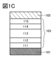


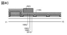

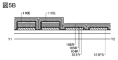


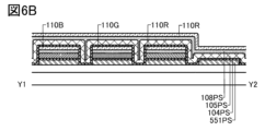

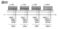


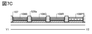


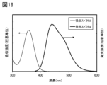
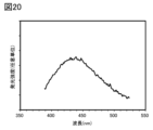


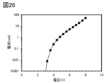


Classifications
-
- C—CHEMISTRY; METALLURGY
- C07—ORGANIC CHEMISTRY
- C07F—ACYCLIC, CARBOCYCLIC OR HETEROCYCLIC COMPOUNDS CONTAINING ELEMENTS OTHER THAN CARBON, HYDROGEN, HALOGEN, OXYGEN, NITROGEN, SULFUR, SELENIUM OR TELLURIUM
- C07F5/00—Compounds containing elements of Groups 3 or 13 of the Periodic Table
- C07F5/02—Boron compounds
-
- C—CHEMISTRY; METALLURGY
- C09—DYES; PAINTS; POLISHES; NATURAL RESINS; ADHESIVES; COMPOSITIONS NOT OTHERWISE PROVIDED FOR; APPLICATIONS OF MATERIALS NOT OTHERWISE PROVIDED FOR
- C09K—MATERIALS FOR MISCELLANEOUS APPLICATIONS, NOT PROVIDED FOR ELSEWHERE
- C09K11/00—Luminescent, e.g. electroluminescent, chemiluminescent materials
- C09K11/06—Luminescent, e.g. electroluminescent, chemiluminescent materials containing organic luminescent materials
-
- H—ELECTRICITY
- H10—SEMICONDUCTOR DEVICES; ELECTRIC SOLID-STATE DEVICES NOT OTHERWISE PROVIDED FOR
- H10K—ORGANIC ELECTRIC SOLID-STATE DEVICES
- H10K50/00—Organic light-emitting devices
-
- C—CHEMISTRY; METALLURGY
- C07—ORGANIC CHEMISTRY
- C07D—HETEROCYCLIC COMPOUNDS
- C07D231/00—Heterocyclic compounds containing 1,2-diazole or hydrogenated 1,2-diazole rings
- C07D231/02—Heterocyclic compounds containing 1,2-diazole or hydrogenated 1,2-diazole rings not condensed with other rings
- C07D231/10—Heterocyclic compounds containing 1,2-diazole or hydrogenated 1,2-diazole rings not condensed with other rings having two or three double bonds between ring members or between ring members and non-ring members
- C07D231/12—Heterocyclic compounds containing 1,2-diazole or hydrogenated 1,2-diazole rings not condensed with other rings having two or three double bonds between ring members or between ring members and non-ring members with only hydrogen atoms, hydrocarbon or substituted hydrocarbon radicals, directly attached to ring carbon atoms
-
- C—CHEMISTRY; METALLURGY
- C07—ORGANIC CHEMISTRY
- C07F—ACYCLIC, CARBOCYCLIC OR HETEROCYCLIC COMPOUNDS CONTAINING ELEMENTS OTHER THAN CARBON, HYDROGEN, HALOGEN, OXYGEN, NITROGEN, SULFUR, SELENIUM OR TELLURIUM
- C07F19/00—Metal compounds according to more than one of main groups C07F1/00 - C07F17/00
-
- C—CHEMISTRY; METALLURGY
- C07—ORGANIC CHEMISTRY
- C07F—ACYCLIC, CARBOCYCLIC OR HETEROCYCLIC COMPOUNDS CONTAINING ELEMENTS OTHER THAN CARBON, HYDROGEN, HALOGEN, OXYGEN, NITROGEN, SULFUR, SELENIUM OR TELLURIUM
- C07F5/00—Compounds containing elements of Groups 3 or 13 of the Periodic Table
Definitions
- One embodiment of the present invention is an organometallic complex, an organic compound, an organic semiconductor element, a light-emitting device, a light-emitting element, an organic EL element, an organic EL element, a photodiode sensor, a light receiving device, a light receiving element, a display module, a lighting module, and a display device. , a light-emitting device, an electronic device, a lighting device, and an electronic device.
- a technical field of one embodiment of the invention disclosed in this specification and the like relates to a product, a method, or a manufacturing method.
- one aspect of the invention relates to a process, machine, manufacture, or composition of matter.
- the technical field of one embodiment of the present invention disclosed in this specification more specifically includes semiconductor devices, display devices, liquid crystal display devices, light-emitting devices, lighting devices, power storage devices, storage devices, imaging devices, and the like. Driving methods or their manufacturing methods can be mentioned as an example.
- Light-emitting devices also referred to as light-emitting elements or organic EL elements
- EL electroluminescence
- the basic structure of these light-emitting devices is to sandwich an organic compound layer (EL layer) containing a light-emitting material between a pair of electrodes.
- EL layer organic compound layer
- an organic EL element is self-luminous, a display device using the element as a pixel has higher visibility than a liquid crystal display device and does not require a backlight. Another great advantage of a display device using such an organic EL element is that it can be made thin and light. Another feature is its extremely fast response speed.
- organic EL devices can continuously form a light-emitting layer in a planar shape, planar light emission can be obtained. Since this is a feature that is difficult to obtain with point light sources such as incandescent lamps and LEDs, or linear light sources such as fluorescent lamps, it is highly useful as a surface light source that can be applied to illumination and the like.
- display devices and lighting devices using organic EL elements are suitable for various electronic devices, and research and development are proceeding in search of organic EL elements having better characteristics.
- Non-Patent Document 1 reports on an organic EL device using a lanthanide complex as a new light-emitting dopant.
- Non-Patent Document 1 As described in Non-Patent Document 1, the application of these organic complexes to light-emitting substances (also referred to as dopants) of organic EL devices has been studied in very few cases, and sufficient studies have not yet been conducted. Therefore, these organic complexes have much room for improvement in performance related to display quality such as chromaticity or color purity, and development is awaited.
- one embodiment of the present invention provides a novel organometallic complex. Further, one embodiment of the present invention provides a novel organometallic complex that can be used for a light-emitting device. Further, one embodiment of the present invention provides a novel organometallic complex that can be used for an EL layer of a light-emitting device. Another object of one embodiment of the present invention is to improve the emission efficiency of a light-emitting device. Another object of one embodiment of the present invention is to improve the reliability of a light-emitting device. Another aspect of the present invention provides a novel light-emitting device.
- an object of one embodiment of the present invention is to provide a light-emitting device with high emission efficiency.
- Another object of one embodiment of the present invention is to provide a light-emitting device, a light-emitting device, an electronic device, a display device, and an electronic device with low power consumption.
- One embodiment of the present invention is an organometallic complex represented by General Formula (G1).
- X represents carbon or nitrogen, where the carbon is hydrogen (including deuterium), a substituted or unsubstituted alkyl group having 1 to 10 carbon atoms, or a substituted or unsubstituted 3 to 10 carbon atoms or a substituted or unsubstituted aryl group having 6 to 30 carbon atoms.
- R 1 to R 3 are each independently hydrogen (including deuterium), a substituted or unsubstituted alkyl group having 1 to 10 carbon atoms, a substituted or unsubstituted cycloalkyl group having 3 to 10 carbon atoms, and a substituted or any one of unsubstituted aryl groups having 6 to 30 carbon atoms.
- n represents an integer of 1 or more and 4 or less.
- each borate ligand may be the same or different.
- n of each borate ligand may be the same or different.
- X of each borate ligand may be the same or different, and R 1 of each borate ligand may be the same or different.
- R2 of each borate ligand may be the same or different from each other.
- R 3 of each borate ligand may be the same or different.
- Another embodiment of the present invention is an organometallic complex represented by General Formula (G2).
- R 1 to R 3 are each independently hydrogen (including deuterium), a substituted or unsubstituted alkyl group having 1 to 10 carbon atoms, a substituted or unsubstituted cyclo represents any one of an alkyl group and a substituted or unsubstituted aryl group having 6 to 30 carbon atoms; Moreover, n represents an integer of 1 or more and 4 or less.
- each borate ligand may be the same or different.
- n of each borate ligand may be the same or different.
- X of each borate ligand may be the same or different
- R 1 of each borate ligand may be the same or different.
- R2 of each borate ligand may be the same or different from each other.
- R 3 of each borate ligand may be the same or different.
- Another embodiment of the present invention is an organometallic complex represented by General Formula (G3).
- X 1 to X 3 each independently represent carbon or nitrogen, and the carbons are each independently hydrogen (including deuterium) or a substituted or unsubstituted alkyl group having 1 to 10 carbon atoms , a substituted or unsubstituted cycloalkyl group having 3 to 10 carbon atoms, or a substituted or unsubstituted aryl group having 6 to 30 carbon atoms.
- R 11 to R 13 , R 21 to R 23 and R 31 to R 33 are each independently hydrogen (including deuterium), substituted or unsubstituted alkyl group having 1 to 10 carbon atoms, substituted or unsubstituted represents any one of a cycloalkyl group having 3 to 10 carbon atoms and a substituted or unsubstituted aryl group having 6 to 30 carbon atoms.
- j, k, and p each independently represents an integer of 1 or more and 4 or less. When j is 2 or more, each X 1 may be the same or different, each R 11 may be the same or different, and each R 12 may be They may be the same or different.
- each X2 may be the same or different, each R21 may be the same or different, and each R22 may be They may be the same or different.
- each X 3 may be the same or different, each R 31 may be the same or different, and each R 32 may be They may be the same or different.
- each R 13 may be the same or different.
- each R 23 may be the same or different.
- each R 33 may be the same or different.
- Another embodiment of the present invention is an organometallic complex represented by General Formula (G3′).
- X 1 to X 3 each independently represent carbon or nitrogen, and the carbons are each independently hydrogen (including deuterium), substituted or unsubstituted alkyl having 1 to 10 carbon atoms group, a substituted or unsubstituted C3-C10 cycloalkyl group, or a substituted or unsubstituted C6-C30 aryl group.
- R 11 to R 13 , R 21 to R 23 and R 31 to R 33 are each independently hydrogen (including deuterium), substituted or unsubstituted alkyl group having 1 to 10 carbon atoms, substituted or unsubstituted represents any one of a cycloalkyl group having 3 to 10 carbon atoms and a substituted or unsubstituted aryl group having 6 to 30 carbon atoms.
- j represents an integer of 1 or more and 3 or less.
- k and p each independently represents an integer of 1 or more and 4 or less.
- each X 1 may be the same or different
- each R 11 may be the same or different
- each R 12 may be They may be the same or different.
- each X2 may be the same or different, each R21 may be the same or different, and each R22 may be They may be the same or different.
- each X 3 may be the same or different, each R 31 may be the same or different, and each R 32 may be They may be the same or different.
- each R 13 may be the same or different.
- each R 23 may be the same or different.
- each R 33 may be the same or different.
- Another embodiment of the present invention is an organometallic complex represented by General Formula (G4).
- X 2 and X 3 each independently represent carbon or nitrogen, and the carbons are each independently hydrogen (including deuterium) or a substituted or unsubstituted alkyl group having 1 to 10 carbon atoms , a substituted or unsubstituted cycloalkyl group having 3 to 10 carbon atoms, or a substituted or unsubstituted aryl group having 6 to 30 carbon atoms.
- R 11 to R 13 , R 21 to R 23 and R 31 to R 33 are each independently hydrogen (including deuterium), substituted or unsubstituted alkyl group having 1 to 10 carbon atoms, substituted or unsubstituted represents any one of a cycloalkyl group having 3 to 10 carbon atoms and a substituted or unsubstituted aryl group having 6 to 30 carbon atoms.
- j, k, and p each independently represents an integer of 1 or more and 4 or less. When j is 2 or more, each R 11 may be the same or different, and each R 12 may be the same or different.
- each X2 may be the same or different, each R21 may be the same or different, and each R22 may be They may be the same or different.
- each X 3 may be the same or different, each R 31 may be the same or different, and each R 32 may be They may be the same or different.
- each R 13 may be the same or different.
- each R 23 may be the same or different.
- each R 33 may be the same or different.
- Another embodiment of the present invention is an organometallic complex represented by General Formula (G5).
- X 11 to X 13 , X 21 to X 23 , X 31 and X 32 each independently represent carbon or nitrogen, and the carbons are each independently hydrogen (including deuterium), substituted or any one of an unsubstituted alkyl group having 1 to 10 carbon atoms, a substituted or unsubstituted cycloalkyl group having 3 to 10 carbon atoms, and a substituted or unsubstituted aryl group having 6 to 30 carbon atoms.
- R 41 to R 47 , R 51 to R 57 and R 61 to R 66 are each independently hydrogen (including deuterium), substituted or unsubstituted alkyl group having 1 to 10 carbon atoms, substituted or unsubstituted represents any one of a cycloalkyl group having 3 to 10 carbon atoms and a substituted or unsubstituted aryl group having 6 to 30 carbon atoms.
- Another embodiment of the present invention is an organometallic complex represented by Structural Formulas (125) and (150).
- Another embodiment of the present invention is a light-emitting device using the organic compound having any of the above structures.
- Another embodiment of the present invention is a light-emitting device including a light-emitting device having any of the above structures, a transistor, or a substrate.
- Another embodiment of the present invention is an electronic device including the light-emitting device having any of the above structures, and a detection portion, an input portion, or a communication portion.
- Another embodiment of the present invention is a lighting device including the light-emitting device with any of the above structures and a housing.
- the light-emitting device in this specification includes an image display device using a light-emitting device.
- a module in which an IC (integrated circuit) is directly mounted by the Glass method may also be included in the light emitting device.
- lighting fixtures and the like may have light emitting devices.
- One embodiment of the present invention can provide a novel organometallic complex. Further, one embodiment of the present invention can provide a novel organometallic complex that can be used for a light-emitting device. Further, according to one embodiment of the present invention, a novel organometallic complex that can be used for an EL layer of a light-emitting device can be provided. Further, in one embodiment of the present invention, the luminous efficiency of the light-emitting device can be improved. Further, according to one embodiment of the present invention, the reliability of the light-emitting device can be improved. Further, according to one embodiment of the present invention, a novel light-emitting device can be provided.
- a light-emitting device with high emission efficiency can be provided.
- a light-emitting device, a light-emitting device, an electronic device, a display device, and an electronic device with low power consumption can be provided.
- 1A to 1E are diagrams illustrating the configuration of a light emitting device according to an embodiment.
- 2A to 2D are diagrams for explaining the light emitting device according to the embodiment.
- 3A to 3C are diagrams for explaining the method for manufacturing the light emitting device according to the embodiment.
- 4A to 4C are diagrams for explaining the method for manufacturing the light emitting device according to the embodiment.
- 5A to 5C are diagrams for explaining the method for manufacturing the light emitting device according to the embodiment.
- 6A to 6D are diagrams for explaining the method for manufacturing the light emitting device according to the embodiment.
- 7A to 7D are diagrams illustrating the light emitting device according to the embodiment.
- 8A to 8C are diagrams illustrating the light emitting device according to the embodiment.
- FIG. 9A to 9F are diagrams for explaining the device and pixel arrangement according to the embodiment.
- 10A to 10C are diagrams illustrating pixel circuits according to embodiments.
- 11A and 11B are diagrams for explaining a light emitting device according to an embodiment.
- FIG. 12A to 12E are diagrams illustrating electronic devices according to embodiments.
- 13A to 13E are diagrams illustrating electronic devices according to embodiments.
- 14A and 14B are diagrams for explaining the electronic device according to the embodiment.
- 15A and 15B are diagrams illustrating the lighting device according to the embodiment.
- FIGS. 18A and 18B are diagrams illustrating a light-emitting device and a light-receiving device according to an embodiment.
- FIG. 19 shows absorption and emission spectra of a dichloromethane solution of [Ce(bpz 3 ) 2 (bpz 2 )].
- FIG. 20 is an emission spectrum of a dichloromethane solution of [Ce(btaz 3 ) 2 (btaz 2 )].
- FIG. 21 is an emission spectrum of [Ce(btaz 3 ) 2 (btaz 2 )] powder.
- FIG. 22 is a diagram illustrating the configuration of the light emitting device 1.
- FIG. FIG. 23 is a diagram showing luminance-current density characteristics of the light-emitting device 1.
- FIG. 24 is a diagram showing the current efficiency-luminance characteristics of the light-emitting device 1.
- FIG. FIG. 25 is a diagram showing luminance-voltage characteristics of the light-emitting device 1.
- FIG. 26 is a diagram showing current-voltage characteristics of the light-emitting device 1.
- FIG. 27 is a diagram showing the external quantum efficiency-luminance characteristics of the light-emitting device 1.
- FIG. 28 is a diagram showing the emission spectrum of the light emitting device 1.
- Display 1 A display using an organic EL element as a display element (organic EL display) has been put into practical use for a long time. Such displays typically have pixels that exhibit at least three colors of light, red, green, and blue, in order to achieve a full-color display.
- the pixel is provided with a light-emitting device for each emission color, and in a side-by-side display, a so-called separate-painting display, each light-emitting device has a different light-emitting substance according to the emission color of the corresponding pixel. are doing.
- Examples of light-emitting substances used in such light-emitting devices include a fluorescent light-emitting substance that emits light from a singlet excited state, a substance that emits thermally activated delayed fluorescence (TADF), and a substance that emits light from a triplet excited state.
- TADF thermally activated delayed fluorescence
- Phosphorescent substances and the like are mainly used and are being actively studied.
- the ratio of the singlet excited state to the triplet excited state is 1:3.
- the theoretical limit of internal quantum efficiency is known to be 25%.
- a phosphorescent substance can convert a singlet excited state to a triplet excited state by intersystem crossing, so that it can theoretically achieve an internal quantum efficiency of 100%, and a light-emitting device with high luminous efficiency can be obtained. can be done. Therefore, phosphorescent light-emitting materials are often used for red and green light-emitting devices in organic EL displays currently in practical use.
- the first factor is that the triplet state energy is lower than the singlet state energy in ordinary substances. Since blue light emission has high energy, a substance having a triplet excited level higher than that of the other two colors is required in order to obtain light emission from the triplet excited state. Naturally, the singlet excitation level of such a substance exists at a higher position, and a substance having such a level tends to be unstable. Moreover, when a host material is used, the host material needs to be a substance having a triplet excitation level and a singlet excitation level positioned at a higher energy level.
- the second factor is the length of the emission lifetime (also referred to as phosphorescence lifetime) of the phosphorescent substance. Since the transition from the triplet excited state to the singlet ground state is spin-forbidden and the transition from the singlet regular state to the singlet ground state is spin-allowed, phosphorescence has a much longer emission lifetime than fluorescence. (phosphorescence lifetime: ⁇ s, fluorescence lifetime: ⁇ ns). A long phosphorescence lifetime means a long lifetime of triplet excitons. Therefore, in a phosphorescent light-emitting device, the light-emitting substance remains in a high-energy excited state for a long time, which accelerates deterioration of the light-emitting substance itself or surrounding substances.
- the term excited state energy is higher than in the other two colors, so the effect of the exciton lifetime is even more pronounced than in the red and green phosphorescent devices, and the reliability for practical use is not expected. It is still difficult to obtain.
- the TADF material mentioned above is a kind of fluorescent substance because it emits light from a singlet excited state, but it enables reverse intersystem crossing. This makes it possible to convert triplet excitation energy into singlet excitation energy, and theoretically achieves an internal quantum efficiency of 100%, similar to phosphorescent materials. Therefore, a light-emitting device using a TADF material as a dopant and a light-emitting device using a TADF material as a host and a fluorescent light-emitting material as a dopant have been proposed, both of which have resulted in an internal quantum efficiency exceeding 25%.
- TADF materials have the same triplet excitation level problem as phosphorescent materials, and since reverse intersystem crossing is forbidden, TADF materials have long exciton lifetimes, making them as reliable as blue phosphorescent devices. It is currently difficult to secure
- organic complexes of Ce 3+ (4 f1 ) and Eu 2+ (4 f7 ) that emit light by fd transition which is a transition between f orbitals and d orbitals.
- Both the ground state and the excited state of these organic complexes are doublet states, and light is emitted from the doublet excited state.
- a singlet excited level and a triplet excited level are generated from the singlet ground state at a ratio of 1:3. Since both are doublet states, 100% of doublet excited states are theoretically generated without being restricted by the spin selection rule, and 100% internal quantum efficiency is possible.
- transitions between different orbitals are parity-forbidden, but fd transitions are parity-allowed transitions, so the transition speed is high and the exciton lifetime of the organic complexes described above is short.
- the transition speed is comparable to that of fluorescent light-emitting materials and is very fast.
- organic complexes of Ce 3+ (4 f1 ) and Eu 2+ (4 f7 ) that emit from the doublet excited state associated with the f–d transition are capable of 100% internal quantum efficiency and exciton It can be seen that it is a light-emitting substance that is expected to ensure high efficiency and high reliability in light-emitting devices because of its short life.
- one aspect of the present invention provides organic complexes of Ce 3+ with three borate ligands.
- the borate ligand has B - and a group that forms a covalent bond with B - .
- some or all of the groups forming a covalent bond with B ⁇ have lone pairs of electrons that can coordinate to Ce 3+ .
- a heteroaryl group having two or more nitrogen atoms can be used, specifically, either one or both of a pyrazolyl group and a triazolyl group. can be mentioned.
- a borate ligand can be coordinated to Ce 3+ by donating a lone pair of electrons possessed by the nitrogen atom of the pyrazolyl or triazolyl group.
- the total number of pyrazolyl groups and triazolyl groups forming a covalent bond with B- is excessive, the molecular weight of the entire organic complex may increase and the sublimability of the organic complex may deteriorate. Therefore, by synthesizing a borate ligand in which the number of pyrazolyl groups and triazolyl groups is controlled to the target number and coordinating the borate ligand to Ce 3+ , the total number of pyrazolyl groups and triazolyl groups in the entire organic complex is It is preferable to adjust the number of
- the coordination number to Ce 3+ is preferably 7 or more and 9 or less, more preferably 8. Therefore, the total number of pyrazolyl groups and triazolyl groups in the organic complex is preferably 7 or more and 9 or less, more preferably 8.
- the total number of pyrazolyl groups and triazolyl groups in this way an organic complex that is stable and highly sublimable can be provided. Therefore, it is suitable as a light-emitting material for light-emitting devices.
- One or more of the pyrazolyl group and triazolyl group of the borate ligand may be bonded to an alkyl group, a cycloalkyl group, or an aryl group.
- steric hindrance can be controlled and the bond distance between the borate ligand and Ce 3+ can be changed, making it possible to adjust the emission color. Further, by changing the types of these substituents, improvement in reliability can be expected.
- an alkyl group, a cycloalkyl group or an aryl group may be bonded to B- .
- steric hindrance can be controlled and the bond distance between the borate ligand and Ce 3+ can be changed, making it possible to adjust the emission color.
- improvement in reliability of the organometallic complex can be expected.
- one embodiment of the present invention is an organometallic complex represented by General Formula (G1).
- X represents carbon or nitrogen, where the carbon is hydrogen (including deuterium), a substituted or unsubstituted alkyl group having 1 to 10 carbon atoms, or a substituted or unsubstituted 3 to 10 carbon atoms or a substituted or unsubstituted aryl group having 6 to 30 carbon atoms.
- R 1 to R 3 are each independently hydrogen (including deuterium), a substituted or unsubstituted alkyl group having 1 to 10 carbon atoms, a substituted or unsubstituted cycloalkyl group having 3 to 10 carbon atoms, and a substituted or any one of unsubstituted aryl groups having 6 to 30 carbon atoms.
- n represents an integer of 1 or more and 4 or less.
- each borate ligand may be the same or different.
- n of each borate ligand may be the same or different.
- X of each borate ligand may be the same or different, and R 1 of each borate ligand may be the same or different.
- R2 of each borate ligand may be the same or different from each other.
- R 3 of each borate ligand may be the same or different.
- Another embodiment of the present invention is an organometallic complex represented by General Formula (G2).
- R 1 to R 3 are each independently hydrogen (including deuterium), a substituted or unsubstituted alkyl group having 1 to 10 carbon atoms, a substituted or unsubstituted cyclo represents any one of an alkyl group and a substituted or unsubstituted aryl group having 6 to 30 carbon atoms; Moreover, n represents an integer of 1 or more and 4 or less.
- each borate ligand may be the same or different.
- n of each borate ligand may be the same or different.
- X of each borate ligand may be the same or different
- R 1 of each borate ligand may be the same or different.
- R2 of each borate ligand may be the same or different from each other.
- R 3 of each borate ligand may be the same or different.
- a Ce 3+ organic complex having a borate ligand having a triazolyl group may reduce the ligand field splitting, so the molar extinction coefficient can be increased.
- the total number of pyrazolyl groups and triazolyl groups in the Ce 3+ organic complex is preferably 7 or more and 9 or less, more preferably 8. Therefore, in general formulas (G1) and (G2), the sum of three n's is preferably 7 or more and 9 or less, more preferably 8.
- Another embodiment of the present invention is an organometallic complex represented by General Formula (G3).
- X 1 to X 3 each independently represent carbon or nitrogen, and the carbons are each independently hydrogen (including deuterium) or a substituted or unsubstituted alkyl group having 1 to 10 carbon atoms , a substituted or unsubstituted cycloalkyl group having 3 to 10 carbon atoms, or a substituted or unsubstituted aryl group having 6 to 30 carbon atoms.
- R 11 to R 13 , R 21 to R 23 and R 31 to R 33 are each independently hydrogen (including deuterium), substituted or unsubstituted alkyl group having 1 to 10 carbon atoms, substituted or unsubstituted represents any one of a cycloalkyl group having 3 to 10 carbon atoms and a substituted or unsubstituted aryl group having 6 to 30 carbon atoms.
- j, k, and p each independently represents an integer of 1 or more and 4 or less. When j is 2 or more, each X 1 may be the same or different, each R 11 may be the same or different, and each R 12 may be They may be the same or different.
- each X2 may be the same or different, each R21 may be the same or different, and each R22 may be They may be the same or different.
- each X 3 may be the same or different, each R 31 may be the same or different, and each R 32 may be They may be the same or different.
- each R 13 may be the same or different.
- each R 23 may be the same or different.
- each R 33 may be the same or different.
- Another embodiment of the present invention is an organometallic complex represented by General Formula (G3′).
- X 1 to X 3 each independently represent carbon or nitrogen, and the carbons are each independently hydrogen (including deuterium), substituted or unsubstituted alkyl having 1 to 10 carbon atoms group, a substituted or unsubstituted C3-C10 cycloalkyl group, or a substituted or unsubstituted C6-C30 aryl group.
- R 11 to R 13 , R 21 to R 23 and R 31 to R 33 are each independently hydrogen (including deuterium), substituted or unsubstituted alkyl group having 1 to 10 carbon atoms, substituted or unsubstituted represents any one of a cycloalkyl group having 3 to 10 carbon atoms and a substituted or unsubstituted aryl group having 6 to 30 carbon atoms.
- j represents an integer of 1 or more and 3 or less.
- k and p each independently represents an integer of 1 or more and 4 or less.
- each X 1 may be the same or different
- each R 11 may be the same or different
- each R 12 may be They may be the same or different.
- each X2 may be the same or different, each R21 may be the same or different, and each R22 may be They may be the same or different.
- each X 3 may be the same or different, each R 31 may be the same or different, and each R 32 may be They may be the same or different.
- each R 13 may be the same or different.
- each R 23 may be the same or different.
- each R 33 may be the same or different.
- Another embodiment of the present invention is an organometallic complex represented by General Formula (G4).
- X 2 and X 3 each independently represent carbon or nitrogen, and the carbons are each independently hydrogen (including deuterium) or a substituted or unsubstituted alkyl group having 1 to 10 carbon atoms , a substituted or unsubstituted cycloalkyl group having 3 to 10 carbon atoms, or a substituted or unsubstituted aryl group having 6 to 30 carbon atoms.
- R 11 to R 13 , R 21 to R 23 and R 31 to R 33 are each independently hydrogen (including deuterium), substituted or unsubstituted alkyl group having 1 to 10 carbon atoms, substituted or unsubstituted represents any one of a cycloalkyl group having 3 to 10 carbon atoms and a substituted or unsubstituted aryl group having 6 to 30 carbon atoms.
- j, k, and p each independently represents an integer of 1 or more and 4 or less. When j is 2 or more, each R 11 may be the same or different, and each R 12 may be the same or different.
- each X2 may be the same or different, each R21 may be the same or different, and each R22 may be They may be the same or different.
- each X 3 may be the same or different, each R 31 may be the same or different, and each R 32 may be They may be the same or different.
- each R 13 may be the same or different.
- each R 23 may be the same or different.
- each R 33 may be the same or different.
- a Ce 3+ organic complex having a borate ligand having at least one triazolyl group such as the organometallic complex represented by the general formula (G4), may reduce the ligand field splitting. Therefore, the molar extinction coefficient can be increased.
- the total number of pyrazolyl groups and triazolyl groups in the Ce 3+ organic complex is preferably 7 or more and 9 or less, more preferably 8. Therefore, in general formulas (G3), (G3′) and (G4), the sum of j, k and p is preferably 7 or more and 9 or less, more preferably 8.
- Another embodiment of the present invention is an organometallic complex represented by General Formula (G5).
- X 11 to X 13 , X 21 to X 23 , X 31 and X 32 each independently represent carbon or nitrogen, and the carbons are each independently hydrogen (including deuterium), substituted or any one of an unsubstituted alkyl group having 1 to 10 carbon atoms, a substituted or unsubstituted cycloalkyl group having 3 to 10 carbon atoms, and a substituted or unsubstituted aryl group having 6 to 30 carbon atoms.
- R 41 to R 47 , R 51 to R 57 and R 61 to R 66 are each independently hydrogen (including deuterium), substituted or unsubstituted alkyl group having 1 to 10 carbon atoms, substituted or unsubstituted represents any one of a cycloalkyl group having 3 to 10 carbon atoms and a substituted or unsubstituted aryl group having 6 to 30 carbon atoms.
- the coordination number of Ce 3+ can be eight, which is preferable. With such a structure, an organometallic complex that is stable and highly sublimable can be obtained. Therefore, the organometallic complex can be used as a light-emitting material suitable for a light-emitting device.
- alkyl groups having 1 to 10 carbon atoms include methyl group, ethyl group, propyl group, isopropyl group, butyl group, sec-butyl group and isobutyl group.
- tert-butyl group pentyl group, isopentyl group, sec-pentyl group, tert-pentyl group, neopentyl group, hexyl group, isohexyl group, sec-hexyl group, tert-hexyl group, neohexyl group, 3-methylpentyl group, 2-methylpentyl group, 2-ethylbutyl group, 1,2-dimethylbutyl group, 2,3-dimethylbutyl group and the like.
- the substituent is an alkyl group having 1 to 4 carbon atoms, a cycloalkyl group having 3 to 6 carbon atoms, or an aryl group having 6 to 13 carbon atoms.
- cycloalkyl group having 3 to 10 carbon atoms include a cyclopropyl group, a cyclobutyl group, a methylcyclobutyl group, a cyclopentyl group, a methylcyclopentyl group, and an isopropylcyclopentyl group.
- the substituent is an alkyl group having 1 to 4 carbon atoms, a cycloalkyl group having 3 to 6 carbon atoms, or an aryl group having 6 to 13 carbon atoms. based on.
- the aryl group having 6 to 30 carbon atoms includes a phenyl group, an o-tolyl group, an m-tolyl group, a p-tolyl group, a mesityl group, and an o-biphenyl group.
- aryl group having 6 to 30 carbon atoms has a substituent, the substituent is an alkyl group having 1 to 4 carbon atoms, a cycloalkyl group having 3 to 6 carbon atoms, or an aryl group having 6 to 13 carbon atoms.
- the steric hindrance in the organometallic complex can be controlled, and the bond distance between the borate ligand and Ce 3+ can be changed, making it possible to adjust the emission color. Further, by introducing these substituents, improvement in reliability of the organometallic complex can be expected. For example, by introducing a methyl group, moderate steric hindrance can be obtained, so that the reliability of the organometallic complex can be improved.
- organometallic complexes of one embodiment of the present invention and the organometallic complexes that can be used for a light-emitting device, which have structures represented by any of the above general formulas (G1) to (G5), are given below. shown in
- organometallic complexes represented by the structural formulas (100) to (179) are specific examples of the structures represented by the general formulas (G1) to (G5), and are one embodiment of the present invention. is not limited to this.
- X represents carbon or nitrogen, where the carbon is hydrogen (including deuterium), a substituted or unsubstituted alkyl group having 1 to 10 carbon atoms, or a substituted or unsubstituted 3 to 10 carbon atoms or a substituted or unsubstituted aryl group having 6 to 30 carbon atoms.
- R 1 to R 3 are each independently hydrogen (including deuterium), a substituted or unsubstituted alkyl group having 1 to 10 carbon atoms, a substituted or unsubstituted cycloalkyl group having 3 to 10 carbon atoms, and a substituted or any one of unsubstituted aryl groups having 6 to 30 carbon atoms.
- n represents an integer of 1 or more and 4 or less.
- each borate ligand may be the same or different.
- n of each borate ligand may be the same or different.
- X of each borate ligand may be the same or different, and R 1 of each borate ligand may be the same or different.
- R2 of each borate ligand may be the same or different from each other.
- R 3 of each borate ligand may be the same or different.
- the organometallic complex of one embodiment of the present invention represented by General Formula (G1) has a heteroaromatic ring represented by General Formula (g1), as shown in Synthesis Scheme (A-1) below.
- a cerium compound a trivalent cerium salt such as cerium(III) chloride, cerium(III) nitrate, and cerium(III) trifluoromethanesulfonate
- one organic solvent such as an alcoholic solvent, tetrahydrofuran, or chloroform
- Organometallic complexes represented by other general formulas can also be synthesized in the same manner as described above.
- Embodiment 2 In this embodiment mode, a structure of a light-emitting device in which a material that emits light from a doublet excited state is used as a light-emitting substance for a light-emitting layer will be described with reference to FIGS. 1A to 1E.
- the light-emitting substance is not particularly limited as long as it emits light from a doublet excited state; however, the organometallic complex described in Embodiment 1 is preferably used.
- FIG. 1A shows a light-emitting device having an EL layer that includes a light-emitting layer between a pair of electrodes. Specifically, it has a structure in which an EL layer 103 is sandwiched between a first electrode 101 and a second electrode 102 .
- FIG. 1B shows a laminated structure (tandem structure) having a plurality of (two layers in FIG. 1B) EL layers (103a and 103b) between a pair of electrodes and a charge generation layer 106 between the EL layers. of the light emitting device.
- a light-emitting device with a tandem structure can realize a highly efficient light-emitting device without changing the amount of current.
- the charge generation layer 106 injects electrons into one EL layer (103a or 103b) and injects electrons into the other EL layer (103b or 103a) has a function of injecting holes. Therefore, in FIG. 1B, when a voltage is applied to the first electrode 101 so that the potential is higher than that of the second electrode 102, electrons are injected from the charge generation layer 106 into the EL layer 103a, and the EL layer 103b is positively charged. A hole is to be injected.
- the charge generation layer 106 may have a property of transmitting visible light (specifically, the visible light transmittance of the charge generation layer 106 is 40% or more). preferable. Also, the charge generation layer 106 functions even with a lower conductivity than the first electrode 101 and the second electrode 102 .
- FIG. 1C shows a layered structure of the EL layer 103 of the light-emitting device which is one embodiment of the present invention.
- the first electrode 101 functions as an anode and the second electrode 102 functions as a cathode.
- the EL layer 103 has a structure in which a hole-injection layer 111, a hole-transport layer 112, a light-emitting layer 113, an electron-transport layer 114, and an electron-injection layer 115 are sequentially stacked over the first electrode 101.
- the light-emitting layer 113 may have a structure in which a plurality of light-emitting layers emitting light of different colors are stacked.
- a light-emitting layer containing a light-emitting substance that emits red light, a light-emitting layer that contains a light-emitting substance that emits green light, and a light-emitting layer that contains a light-emitting substance that emits blue light are stacked, or a layer containing a carrier-transporting material is interposed therebetween. It may be a laminated structure. Alternatively, a light-emitting layer containing a light-emitting substance that emits yellow light and a light-emitting layer containing a light-emitting substance that emits blue light may be combined. However, the laminated structure of the light-emitting layer 113 is not limited to the above.
- the light-emitting layer 113 may have a structure in which a plurality of light-emitting layers emitting light of the same color are stacked.
- a structure in which a first light-emitting layer containing a light-emitting substance that emits blue light and a second light-emitting layer containing a light-emitting substance that emits blue light are stacked or stacked with a layer containing a carrier-transporting material interposed therebetween. It can be.
- reliability may be improved as compared with a single-layer structure.
- each EL layer is stacked sequentially from the anode side as described above.
- the stacking order of the EL layers 103 is reversed.
- 111 on the first electrode 101 which is a cathode is an electron injection layer
- 112 is an electron transport layer
- 113 is a light emitting layer
- 114 is a hole transport layer
- 115 is a hole. It has a configuration of an injection layer.
- the light-emitting layer 113 included in the EL layers (103, 103a, 103b) has an appropriate combination of a plurality of substances including a material that emits light from a doublet excited state.
- a structure in which different emission colors are obtained from the plurality of EL layers (103a and 103b) shown in FIG. 1B may be employed.
- different materials may be used for the light-emitting substance and other substances used in each light-emitting layer.
- the light-emitting device which is one embodiment of the present invention, for example, the first electrode 101 shown in FIG. ) structure
- light emitted from the light emitting layer 113 included in the EL layer 103 can be resonated between the two electrodes, and light emitted from the second electrode 102 can be enhanced.
- the film of the transparent conductive film Optical tuning can be achieved by controlling the thickness. Specifically, the optical distance between the first electrode 101 and the second electrode 102 (the product of the film thickness and the refractive index) is m ⁇ / It is preferable to adjust to 2 (where m is an integer equal to or greater than 1) or its vicinity.
- the optical distance from the first electrode 101 to the region (light-emitting region) of the light-emitting layer 113 from which desired light is obtained (2m′+1) ⁇ /4 (where m′ is an integer equal to or greater than 1) or the vicinity thereof. It is preferable to adjust so that Note that the light-emitting region here means a recombination region of holes and electrons in the light-emitting layer 113 .
- the spectrum of specific monochromatic light obtained from the light-emitting layer 113 can be narrowed, and light emission with good color purity can be obtained.
- the optical distance between the first electrode 101 and the second electrode 102 is the total thickness from the reflection area of the first electrode 101 to the reflection area of the second electrode 102. can.
- the optical distance between the first electrode 101 and the light-emitting layer from which desired light is obtained is the optical distance between the reflection region in the first electrode 101 and the light-emitting region in the light-emitting layer from which desired light is obtained. It can be said that it is the distance.
- an arbitrary position of the first electrode 101 can be set as the reflective region and the desired light.
- an arbitrary position of the light-emitting layer from which light is obtained is the light-emitting region, the above effects can be sufficiently obtained.
- the light-emitting device shown in FIG. 1D is a light-emitting device having a tandem structure and has a microcavity structure, so that light of different wavelengths (monochromatic light) can be extracted from each EL layer (103a, 103b). Therefore, separate coloring (for example, RGB) for obtaining different emission colors is unnecessary. Therefore, it is easy to achieve high definition. A combination with a colored layer (color filter) is also possible. Furthermore, since it is possible to increase the emission intensity of the specific wavelength in the front direction, it is possible to reduce power consumption.
- the light-emitting device shown in FIG. 1E is an example of the tandem structure light-emitting device shown in FIG. It has a structure in which it is sandwiched and laminated.
- the three EL layers (103a, 103b, 103c) each have a light-emitting layer (113a, 113b, 113c), and the emission colors of the respective light-emitting layers can be freely combined.
- light-emitting layer 113a can be blue
- light-emitting layer 113b can be either red, green, or yellow
- light-emitting layer 113c can be blue
- light-emitting layer 113a can be red and light-emitting layer 113b can be blue, green, or yellow.
- the light-emitting layer 113c may be red.
- the first electrode 101 and the second electrode 102 is a light-transmitting electrode (a transparent electrode, a semi-transmissive/semi-reflective electrode, or the like). do.
- the visible light transmittance of the transparent electrode is set to 40% or more.
- the visible light reflectance of the semi-transmissive/semi-reflective electrode should be 20% or more and 80% or less, preferably 40% or more and 70% or less.
- these electrodes preferably have a resistivity of 1 ⁇ 10 ⁇ 2 ⁇ cm or less.
- the reflective electrode when one of the first electrode 101 and the second electrode 102 is a reflective electrode (reflective electrode), the reflective electrode The light reflectance is 40% or more and 100% or less, preferably 70% or more and 100% or less. Moreover, the electrode preferably has a resistivity of 1 ⁇ 10 ⁇ 2 ⁇ cm or less.
- FIG. 1D having a tandem structure.
- the structure of the EL layer is the same for the single-structure light-emitting device shown in FIGS. 1A and 1C.
- the first electrode 101 is formed as a reflective electrode
- the second electrode 102 is formed as a semi-transmissive/semi-reflective electrode. Therefore, a desired electrode material can be used singly or plurally to form a single layer or lamination.
- the second electrode 102 is formed by selecting an appropriate material after the EL layer 103b is formed.
- First electrode and second electrode> As materials for forming the first electrode 101 and the second electrode 102, the following materials can be used in appropriate combination as long as the above-described functions of both electrodes can be satisfied. For example, metals, alloys, electrically conductive compounds, mixtures thereof, and the like can be used as appropriate. Specifically, In--Sn oxide (also referred to as ITO), In--Si--Sn oxide (also referred to as ITSO), In--Zn oxide, and In--W--Zn oxide are given.
- ITO In--Sn oxide
- ITSO In--Si--Sn oxide
- ITSO In--Zn oxide
- In--W--Zn oxide In--W--Zn oxide
- elements belonging to Group 1 or Group 2 of the periodic table of elements not exemplified above e.g., lithium (Li), cesium (Cs), calcium (Ca), strontium (Sr)), europium (Eu), ytterbium Rare earth metals such as (Yb), alloys containing an appropriate combination thereof, graphene, and the like can be used.
- a hole injection layer 111a and a hole transport layer 112a of the EL layer 103a are sequentially stacked on the first electrode 101 by vacuum deposition. be.
- hole injection layer 111b and hole transport layer 112b of EL layer 103b are sequentially laminated on charge generation layer 106 in the same manner.
- the hole injection layers (111, 111a, 111b) inject holes from the first electrode 101, which is an anode, and the charge generation layers (106, 106a, 106b) into the EL layers (103, 103a, 103b). It is a layer containing an organic acceptor material and a material with a high hole injection property.
- the organic acceptor material has a LUMO (Lowest Unoccupied Molecular Orbital) level value and a HOMO (Highest Occupied Molecular Orbital) level value close to other organic compounds. It is a material that can generate holes in the organic compound by causing the organic compound to generate holes. Therefore, compounds having electron-withdrawing groups (halogen groups or cyano groups) such as quinodimethane derivatives, chloranil derivatives, and hexaazatriphenylene derivatives can be used as organic acceptor materials.
- halogen groups or cyano groups such as quinodimethane derivatives, chloranil derivatives, and hexaazatriphenylene derivatives
- a compound in which an electron-withdrawing group is bound to a condensed aromatic ring having a plurality of heteroatoms such as HAT-CN, is suitable because it has a high acceptor property and stable film quality against heat.
- [3] radialene derivatives having an electron-withdrawing group are preferred because of their extremely high electron-accepting properties, specifically ⁇ , ⁇ ', ⁇ '.
- Materials with high hole injection properties include oxides of metals belonging to groups 4 to 8 in the periodic table (molybdenum oxide, vanadium oxide, ruthenium oxide, tungsten oxide, manganese oxide, etc.). transition metal oxides, etc.) can be used. Specific examples include molybdenum oxide, vanadium oxide, niobium oxide, tantalum oxide, chromium oxide, tungsten oxide, manganese oxide, and rhenium oxide. Among the above, molybdenum oxide is preferred because it is stable in the atmosphere, has low hygroscopicity, and is easy to handle. In addition, a phthalocyanine-based compound such as phthalocyanine (abbreviation: H 2 Pc) or copper phthalocyanine (abbreviation: CuPc) can be used.
- H 2 Pc phthalocyanine
- CuPc copper phthalocyanine
- low-molecular-weight compounds such as 4,4′,4′′-tris(N,N-diphenylamino)triphenylamine (abbreviation: TDATA) and 4,4′,4′′-tris [N-(3-methylphenyl)-N-phenylamino]triphenylamine (abbreviation: MTDATA), 4,4′-bis[N-(4-diphenylaminophenyl)-N-phenylamino]biphenyl (abbreviation: DPAB), N,N′-bis[4-bis(3-methylphenyl)aminophenyl]-N,N′-diphenyl-4,4′-diaminobiphenyl (abbreviation: DNTPD), 1,3,5-tris [N-(4-diphenylaminophenyl)-N-phenylamino]benzene (abbreviation: DPA3B), 3-[N-(9-phenyl
- poly(N-vinylcarbazole) (abbreviation: PVK)
- poly(4-vinyltriphenylamine) (abbreviation: PVTPA)
- PVTPA poly(4-vinyltriphenylamine)
- PTPDMA poly[N-(4 - ⁇ N'-[4-(4-diphenylamino)phenyl]phenyl-N'-phenylamino ⁇ phenyl)methacrylamide]
- PTPDMA poly[N,N'-bis(4-butylphenyl)- N,N'-bis(phenyl)benzidine]
- Poly-TPD poly(N-vinylcarbazole) or the like
- PEDOT/PSS poly(3,4-ethylenedioxythiophene)/polystyrene sulfonic acid
- PAni/PSS polyaniline/polystyrene sulfonic acid
- other acid-added polymer compounds etc.
- a mixed material containing a hole-transporting material and the above-described organic acceptor material can also be used.
- electrons are extracted from the hole-transporting material by the organic acceptor material, holes are generated in the hole-injection layer 111 , and holes are injected into the light-emitting layer 113 via the hole-transporting layer 112 .
- the hole injection layer 111 may be formed of a single layer made of a mixed material containing a hole-transporting material and an organic acceptor material (electron-accepting material). (electron-accepting material) may be laminated in separate layers.
- the hole-transporting material a substance having a hole mobility of 1 ⁇ 10 ⁇ 6 cm 2 /Vs or more at a square root of an electric field strength [V/cm] of 600 is preferable. Note that any substance other than these can be used as long as it has a higher hole-transport property than electron-transport property.
- hole-transporting materials include compounds having a ⁇ -electron-rich heteroaromatic ring (e.g., carbazole derivatives, furan derivatives, or thiophene derivatives), and positive compounds such as aromatic amines (organic compounds having an aromatic amine skeleton). Materials with high pore transport properties are preferred.
- carbazole derivatives organic compounds having a carbazole ring
- examples of the carbazole derivatives include bicarbazole derivatives (eg, 3,3'-bicarbazole derivatives) and aromatic amines having a carbazolyl group.
- bicarbazole derivative for example, 3,3′-bicarbazole derivative
- PCCP 3,3′-bis(9-phenyl-9H-carbazole)
- BisBPCz 9,9 '-bis(biphenyl-4-yl)-3,3'-bi-9H-carbazole
- BismBPCz 9,9'-bis(1,1'-biphenyl-3-yl)-3,3' -bi-9H-carbazole
- BismBPCz 9-(1,1′-biphenyl-3-yl)-9′-(1,1′-biphenyl-4-yl)-9H,9′H-3 ,3′-bicarbazole
- mBPCCBP 9,2-naphthyl)-9′-phenyl-9H,9′H-3,3′-bicarbazole
- ⁇ NCCP 9-(2-naphthyl)-9′-phenyl-9H,9′H-3,3′-bicarbazol
- aromatic amine having a carbazolyl group examples include 4-phenyl-4′-(9-phenyl-9H-carbazol-3-yl)triphenylamine (abbreviation: PCBA1BP), N-( 4-biphenyl)-N-(9,9-dimethyl-9H-fluoren-2-yl)-9-phenyl-9H-carbazol-3-amine (abbreviation: PCBiF), N-(biphenyl-4-yl)- N-[4-(9-phenyl-9H-carbazol-3-yl)phenyl]-9,9-dimethyl-9H-fluoren-2-amine (abbreviation: PCBBiF), N-[4-(9-phenyl- 9H-carbazol-3-yl)phenyl]-bis(9,9-dimethyl-9H-fluoren-2-yl)amine (abbreviation: PCBFF), N-(1,1′-biphenyl-4-
- PCPPn 9-[4-(9-phenyl-9H-carbazol-3-yl)-phenyl]phenanthrene
- PCPN 3-[4-(1-naphthyl) -Phenyl]-9-phenyl-9H-carbazole
- mCP 1,3-bis(N-carbazolyl)benzene
- CBP 4,4′-di(N-carbazolyl)biphenyl
- CzTP 3,6-bis(3,5-diphenylphenyl)-9-phenylcarbazole
- TCPB 9-[4-(10-phenyl-9-anthracenyl)phenyl]-9H-carbazole
- furan derivative organic compound having a furan ring
- DBF3P- II 4,4′,4′′-(benzene-1,3,5-triyl)tri(dibenzofuran)
- mmDBFFLBi-II 4- ⁇ 3-[3-(9-phenyl-9H-fluoren-9-yl)phenyl]phenyl ⁇ dibenzofuran
- thiophene derivative an organic compound having a thiophene ring
- DBT3P 4,4′,4′′-(benzene-1,3,5-triyl)tri(dibenzothiophene)
- DBT3P 4,4′,4′′-(benzene-1,3,5-triyl)tri(dibenzothiophene)
- DBTFLP-III 2,8-diphenyl-4-[4-(9-phenyl-9H-fluoren-9-yl)phenyl]dibenzothiophene
- DBTFLP-III 4-[4-(9-phenyl- 9H-fluoren-9-yl)phenyl]-6-phenyldibenzothiophene
- DBTFLP-IV 4-[4-(9-phenyl- 9H-fluoren-9-yl)phenyl]-6-phenyldibenzothiophene
- aromatic amine examples include 4,4′-bis[N-(1-naphthyl)-N-phenylamino]biphenyl (abbreviation: NPB or ⁇ -NPD), N,N′- Diphenyl-N,N'-bis(3-methylphenyl)-4,4'-diaminobiphenyl (abbreviation: TPD), N,N'-bis(9,9'-spirobi[9H-fluoren]-2-yl )-N,N′-diphenyl-4,4′-diaminobiphenyl (abbreviation: BSPB), 4-phenyl-4′-(9-phenylfluoren-9-yl)triphenylamine (abbreviation: BPAFLP), 4- Phenyl-3′-(9-phenylfluoren-9-yl)triphenylamine (abbreviation: mBPAFLP), N-(9,9-dimethyl-9H-
- PVK poly(N-vinylcarbazole)
- PVK poly(4-vinyltriphenylamine)
- PVK high molecular compounds
- PVTPA poly[N-(4- ⁇ N'-[4-(4-diphenylamino)phenyl]phenyl-N'-phenylamino ⁇ phenyl)methacrylamide]
- PTPDMA poly[N,N' -Bis(4-butylphenyl)-N,N'-bis(phenyl)benzidine]
- Poly-TPD poly[N,N' -Bis(4-butylphenyl)-N,N'-bis(phenyl)benzidine]
- PEDOT/PSS poly(3,4-ethylenedioxythiophene)/polystyrene sulfonic acid
- PAni/PSS polyaniline/polystyrene sulfonic acid
- other acid-added polymer compounds etc.
- the hole-transporting material is not limited to the above, and one or a combination of various known materials may be used as the hole-transporting material.
- the hole injection layers (111, 111a, 111b) can be formed using various known film forming methods, and for example, can be formed using a vacuum deposition method.
- the hole transport layers (112, 112a, 112b) transfer holes injected from the first electrode 101 to the light emitting layers (113, 113a, 113b, 113c) by the hole injection layers (111, 111a, 111b). This is the transport layer.
- the hole-transporting layers (112, 112a, 112b) are layers containing a hole-transporting material. Therefore, for the hole transport layers (112, 112a, 112b), a hole transport material that can be used for the hole injection layers (111, 111a, 111b) can be used.
- the same organic compound as that for the hole-transport layers (112, 112a, and 112b) can be used for the light-emitting layers (113, 113a, 113b, and 113c).
- the hole transport layers (112, 112a, 112b) and the light emitting layers (113, 113a, 113b, 113c) can be efficiently transported, which is more preferable.
- the light-emitting layers (113, 113a, 113b, 113c) are layers containing light-emitting substances.
- a material that emits light from a doublet excited state can be used as the light-emitting substance.
- the light-emitting substance is not particularly limited as long as it emits light from a doublet excited state; however, the organometallic complex described in Embodiment 1 is preferably used.
- the light-emitting layers (113, 113a, 113b, 113c) may contain one or more organic compounds (host material, etc.) in addition to the light-emitting substance (guest material).
- organic compound used as the host material a hole-transporting material that can be used in the hole-transporting layers (112, 112a, 112b) described above, or a hole-transporting material that can be used in the above-described hole-transporting layers (112, 112a, 112b) as long as it satisfies the conditions as a host material used in the light-emitting layer.
- organic compounds such as electron-transporting materials that can be used for the electron-transporting layers (114, 114a, 114b) of .
- the present inventors have found that when a material that emits light from a doublet excited state is used as a light-emitting substance in the light-emitting layer, the host material preferably contains an electron-transporting heteroaromatic compound. Considering the carrier-transporting properties of the doublet light-emitting material, the host material preferably transports electrons, and the heteroaromatic ring is stable as the electron-transporting skeleton. As the electron-transporting heteroaromatic compound used as the host material, a ⁇ -electron-deficient heteroaromatic compound is preferably used. Note that the light-emitting substance in this case is not particularly limited as long as it emits light from a doublet excited state; however, the organometallic complex described in Embodiment 1 is preferable.
- ⁇ -electron-deficient heteroaromatic compounds include, for example, phenanthroline derivatives, quinoline derivatives, benzoquinoline derivatives, quinoxaline derivatives, dibenzoquinoxaline derivatives, pyridine derivatives, bipyridine derivatives, diazine (pyrimidine, pyrazine, pyridazine) derivatives, Compounds containing nitrogen-containing six-membered heteroaromatic rings, such as triazine derivatives, can be mentioned.
- the heteroaromatic ring of these derivatives may be further condensed with an aromatic ring such as a benzene ring.
- ⁇ -electron-deficient heteroaromatic compound examples include a ⁇ -electron-deficient heteroaromatic compound can be obtained from an organic compound such as the above-described hole-transporting material or the below-described electron-transporting material. can be selected.
- the electron transport layers (114, 114a, 114b) transfer electrons injected from the second electrode 102 and the charge generation layers (106, 106a, 106b) by the electron injection layers (115, 115a, 115b) described later into the light emitting layer ( 113, 113a, 113b, 113c).
- the heat resistance of the light-emitting device which is one embodiment of the present invention, can be improved when the electron-transport layer has a layered structure.
- the electron transporting material used for the electron transporting layers (114, 114a, 114b) has an electron mobility of 1 ⁇ 10 ⁇ 6 cm 2 /Vs or more when the square root of the electric field strength [V/cm] is 600.
- a substance with a degree of hardness is preferred. Note that any substance other than these substances can be used as long as it has a higher electron-transport property than hole-transport property.
- the electron transport layers (114, 114a, 114b) function as a single layer, but may have a laminated structure of two or more layers. Since the above mixed material has heat resistance, the effect of the heat process on the device characteristics can be suppressed by performing a photolithography process on the electron transport layer using the mixed material.
- an organic compound having a high electron-transporting property can be used, and for example, a heteroaromatic compound can be used.
- a heteroaromatic compound is a cyclic compound containing at least two different elements in the ring.
- the ring structure includes a 3-membered ring, a 4-membered ring, a 5-membered ring, a 6-membered ring, etc., and a 5-membered ring or a 6-membered ring is particularly preferable.
- Heteroaromatic compounds containing any one or more of nitrogen, oxygen, or sulfur are preferred.
- nitrogen-containing heteroaromatic compounds nitrogen-containing heteroaromatic compounds
- materials with high electron transport properties such as nitrogen-containing heteroaromatic compounds or ⁇ -electron deficient heteroaromatic compounds containing these (electron transport properties material) is preferably used.
- a material different from the material used for the light-emitting layer can also be used for this electron-transporting material. Not all excitons generated by recombination of carriers in the light-emitting layer can contribute to light emission, and may diffuse into layers in contact with or in the vicinity of the light-emitting layer. In order to avoid this phenomenon, the electron transport material is preferably different from the material used for the light-emitting layer. This makes it possible to obtain a highly efficient device.
- a heteroaromatic compound is an organic compound having at least one heteroaromatic ring.
- the heteroaromatic ring has any one of a pyridine ring, a diazine ring, a triazine ring, a polyazole ring, an oxazole ring, a thiazole ring, and the like.
- heteroaromatic rings having a diazine ring include heteroaromatic rings having a pyrimidine ring, a pyrazine ring, a pyridazine ring, or the like.
- heteroaromatic rings having a polyazole ring include heteroaromatic rings having an imidazole ring, a triazole ring, and an oxadiazole ring.
- a heteroaromatic ring also includes a fused heteroaromatic ring having a fused ring structure.
- the condensed heteroaromatic ring includes quinoline ring, benzoquinoline ring, quinoxaline ring, dibenzoquinoxaline ring, quinazoline ring, benzoquinazoline ring, dibenzoquinazoline ring, phenanthroline ring, furodiazine ring, and benzimidazole ring.
- heteroaromatic compounds having a 5-membered ring structure include heteroaromatic compounds having an imidazole ring compounds, heteroaromatic compounds having a triazole ring, heteroaromatic compounds having an oxazole ring, heteroaromatic compounds having an oxadiazole ring, heteroaromatic compounds having a thiazole ring, heteroaromatic compounds having a benzimidazole ring, etc. is mentioned.
- heteroaromatic compounds having a 6-membered ring structure include a pyridine ring, a diazine ring (pyrimidine ring, pyrazine ring, pyridazine ring, etc.), heteroaromatic compounds having heteroaromatic rings such as triazine ring and polyazole ring. It is included in heteroaromatic compounds having a structure in which pyridine rings are linked, and includes heteroaromatic compounds having a bipyridine structure and heteroaromatic compounds having a terpyridine structure.
- the heteroaromatic compound having a condensed ring structure partially including the six-membered ring structure includes a quinoline ring, a benzoquinoline ring, a quinoxaline ring, a dibenzoquinoxaline ring, a phenanthroline ring, and a (including structures in which aromatic rings are condensed), heteroaromatic compounds having condensed heteroaromatic rings such as benzimidazole rings, and the like.
- heteroaromatic compound having a five-membered ring structure include 2-( 4-biphenylyl)-5-(4-tert-butylphenyl)-1,3,4-oxadiazole (abbreviation: PBD), 1,3-bis[5-(p-tert-butylphenyl)-1, 3,4-oxadiazol-2-yl]benzene (abbreviation: OXD-7), 9-[4-(5-phenyl-1,3,4-oxadiazol-2-yl)phenyl]-9H- Carbazole (abbreviation: CO11), 3-(4-biphenylyl)-4-phenyl-5-(4-tert-butylphenyl)-1,2,4-triazole
- heteroaromatic compound having a 6-membered ring structure including a heteroaromatic ring having a pyridine ring, a diazine ring, a triazine ring, etc.
- the heteroaromatic compound having a 6-membered ring structure include 3,5-bis[3-(9H-carbazole-9 -yl)phenyl]pyridine (abbreviation: 35DCzPPy), 1,3,5-tri[3-(3-pyridyl)phenyl]benzene (abbreviation: TmPyPB), and other heteroaromatics containing a heteroaromatic ring having a pyridine ring Compound, 2- ⁇ 4-[3-(N-phenyl-9H-carbazol-3-yl)-9H-carbazol-9-yl]phenyl ⁇ -4,6-diphenyl-1,3,5-triazine (abbreviation : PCCzPTzn), 9-[3-(4,6-dip
- 2,2′-(pyridine-2,6-diyl)bis(4-phenylbenzo[h]quinazoline) (abbreviation: 2,6(P-Bqn)2Py)
- 2,2′-(2 ,2′-bipyridine-6,6′-diyl)bis(4-phenylbenzo[h]quinazoline) (abbreviation: 6,6′(P-Bqn)2BPy)
- 2,2′-(pyridine-2,6 -diyl)bis ⁇ 4-[4-(2-naphthyl)phenyl]-6-phenylpyrimidine ⁇ (abbreviation: 2,6(NP-PPm)2Py), 6-(biphenyl-3-yl)-4-[ heteroaromatic compounds containing a heteroaromatic ring having a diazine (pyrimidine) ring such as 3,5-bis(9H-carbazol-9-yl)phenyl]-2-phenylpyr
- heteroaromatic compound having a condensed ring structure partially including a six-membered ring structure include bathophenanthroline (abbreviation: Bphen) and bathocuproine (abbreviation: BCP).
- metal complexes shown below can be used in addition to the heteroaromatic compounds shown above.
- Tris(8-quinolinolato)aluminum (III) (abbreviation: Alq3 )
- tris(4-methyl-8-quinolinolato)aluminum (III) (abbreviation: Almq3 )
- 8-quinolinolato-lithium (abbreviation: Liq)
- BeBq 2 , a quinoline ring or benzo
- poly(2,5-pyridinediyl) (abbreviation: PPy), poly[(9,9-dihexylfluorene-2,7-diyl)-co-(pyridine-3,5-diyl)] (abbreviation: PF -Py), poly[(9,9-dioctylfluorene-2,7-diyl)-co-(2,2′-bipyridine-6,6′-diyl)] (abbreviation: PF-BPy)
- PPy poly[(9,9-dihexylfluorene-2,7-diyl)-co-(pyridine-3,5-diyl)]
- PF -BPy poly[(9,9-dioctylfluorene-2,7-diyl)-co-(2,2′-bipyridine-6,6′-diyl)]
- the electron transport layers (114, 114a, 114b) are not limited to a single layer, and may have a structure in which two or more layers made of the above substances are laminated.
- the electron injection layers (115, 115a, 115b) are layers containing substances with high electron injection properties. Further, the electron injection layers (115, 115a, 115b) are layers for increasing the injection efficiency of electrons from the second electrode 102. When comparing the LUMO level values of the materials used for the layers (115, 115a, 115b), it is preferable to use a material with a small difference (0.5 eV or less).
- the electron injection layer 115 includes lithium, cesium, lithium fluoride (LiF), cesium fluoride (CsF), calcium fluoride (CaF 2 ), 8-quinolinolato-lithium (abbreviation: Liq), 2-(2 -pyridyl)phenoratritium (abbreviation: LiPP), 2-(2-pyridyl)-3-pyridinolatritium (abbreviation: LiPPy), 4-phenyl-2-(2-pyridyl)phenoratritium (abbreviation: LiPPP) , lithium oxide (LiO x ), cesium carbonate, etc., alkali metals, alkaline earth metals, or compounds thereof.
- Liq 2-(2 -pyridyl)phenoratritium
- LiPPy 2-(2-pyridyl)-3-pyridinolatritium
- LiPPP 4-phenyl-2-(2-pyridyl)phenoratritium
- rare earth metals or rare earth metal compounds such as erbium fluoride (ErF 3 ) and ytterbium (Yb) can be used.
- the electron injection layers (115, 115a, 115b) may be formed by mixing plural kinds of the above materials, or may be formed by stacking plural kinds of the above materials.
- Electride may also be used for the electron injection layers (115, 115a, 115b). Examples of the electride include a mixed oxide of calcium and aluminum to which electrons are added at a high concentration.
- the substance which comprises the electron transport layer (114, 114a, 114b) mentioned above can also be used.
- a mixed material obtained by mixing an organic compound and an electron donor (donor) may be used for the electron injection layers (115, 115a, 115b).
- a mixed material has excellent electron injection properties and electron transport properties because electrons are generated in the organic compound by the electron donor.
- the organic compound is preferably a material excellent in transporting generated electrons.
- an electron-transporting material metal complex and heteroaromatic compounds, etc.
- the electron donor any substance can be used as long as it exhibits an electron donating property with respect to an organic compound.
- alkali metals, alkaline earth metals and rare earth metals are preferred, and examples include lithium, cesium, magnesium, calcium, erbium, ytterbium and the like.
- alkali metal oxides and alkaline earth metal oxides are preferred, and examples thereof include lithium oxide, calcium oxide and barium oxide.
- Lewis bases such as magnesium oxide can also be used.
- An organic compound such as tetrathiafulvalene (abbreviation: TTF) can also be used. Also, a plurality of these materials may be laminated and used.
- a mixed material obtained by mixing an organic compound and a metal may be used for the electron injection layers (115, 115a, 115b).
- the organic compound used here preferably has a LUMO level of -3.6 eV to -2.3 eV. Also, a material having a lone pair of electrons is preferred.
- the mixed material obtained by mixing the heteroaromatic compound with the metal which can be used for the electron transport layer
- heteroaromatic compounds include heteroaromatic compounds having a 5-membered ring structure (imidazole ring, triazole ring, oxazole ring, oxadiazole ring, thiazole ring, benzimidazole ring, etc.), 6-membered ring structures (pyridine ring, diazine Heteroaromatic compounds having a ring (including pyrimidine ring, pyrazine ring, pyridazine ring, etc.), triazine ring, bipyridine ring, terpyridine ring, etc.; A material having a lone pair of electrons, such as a heteroaromatic compound having a ring, a quinoxaline ring, a dibenzoquinoxaline ring, a phenanthroline ring
- transition metals belonging to Groups 5, 7, 9 or 11 in the periodic table and materials belonging to Group 13.
- materials belonging to Group 13 For example, Ag , Cu, Al, or In.
- SOMO singly occupied molecular orbital
- the optical distance between the second electrode 102 and the light emitting layer 113b is less than 1/4 of the wavelength ⁇ of the light emitted by the light emitting layer 113b. It is preferable to form In this case, it can be adjusted by changing the film thickness of the electron transport layer 114b or the electron injection layer 115b.
- a structure in which a plurality of EL layers are laminated between a pair of electrodes can also be used.
- the charge generation layer 106 injects electrons into the EL layer 103a and injects holes into the EL layer 103b. It has the function of injecting. Note that even if the charge generation layer 106 has a structure in which an electron acceptor (acceptor) is added to a hole-transporting material (also referred to as a P-type layer), an electron donor (donor) is added to the electron-transporting material. A structure (also referred to as an electron injection buffer layer) may be used. Also, both of these configurations may be laminated. Furthermore, an electron relay layer may be provided between the P-type layer and the electron injection buffer layer. Note that by forming the charge-generating layer 106 using the above materials, an increase in driving voltage in the case where EL layers are stacked can be suppressed.
- the hole-transporting material may be any of the materials shown in this embodiment mode. can be used.
- electron acceptors include 7,7,8,8-tetracyano-2,3,5,6-tetrafluoroquinodimethane (abbreviation: F4 -TCNQ), chloranil, and the like.
- F4 -TCNQ 7,7,8,8-tetracyano-2,3,5,6-tetrafluoroquinodimethane
- chloranil and the like.
- oxides of metals belonging to groups 4 to 8 in the periodic table can be mentioned.
- the materials described in this embodiment can be used as the electron-transporting material.
- the electron donor alkali metals, alkaline earth metals, rare earth metals, metals belonging to Groups 2 and 13 in the periodic table, and oxides and carbonates thereof can be used. Specifically, lithium (Li), cesium (Cs), magnesium (Mg), calcium (Ca), ytterbium (Yb), indium (In), lithium oxide (Li 2 O), cesium carbonate, or the like can be used. preferable.
- an organic compound such as tetrathianaphthacene may be used as an electron donor.
- the electron-relay layer contains at least a substance having an electron-transport property, and the electron-injection buffer layer and the P-type layer interact with each other. It has the function of preventing the action and transferring electrons smoothly.
- the LUMO level of the electron-transporting substance contained in the electron relay layer is the same as the LUMO level of the acceptor substance in the P-type layer and the LUMO level of the electron-transporting substance contained in the electron-transporting layer in contact with the charge generation layer 106. It is preferably between the LUMO levels.
- a specific energy level of the LUMO level in the substance having an electron-transporting property used for the electron relay layer is -5.0 eV or more, preferably -5.0 eV or more and -3.0 eV or less. It is preferable to use a phthalocyanine-based material or a metal complex having a metal-oxygen bond and an aromatic ligand as an electron-transporting substance used for the electron-relay layer.
- FIG. 1D shows a structure in which two EL layers 103 are stacked
- a stacked structure of three or more EL layers may be employed by providing a charge generation layer between different EL layers.
- a cap layer may be provided over the second electrode 102 of the light emitting device.
- a material with a high refractive index can be used for the cap layer.
- cap layer examples include 5,5′-diphenyl-2,2′-di-5H-[1]benzothieno[3,2-c]carbazole (abbreviation: BisBTc), 4,4 ',4''-(benzene-1,3,5-triyl)tri(dibenzothiophene) (abbreviation: DBT3P-II) and the like.
- BisBTc 5,5′-diphenyl-2,2′-di-5H-[1]benzothieno[3,2-c]carbazole
- DBT3P-II 4,4 ',4''-(benzene-1,3,5-triyl)tri(dibenzothiophene)
- the light-emitting device described in this embodiment can be formed over various substrates.
- the type of substrate is not limited to a specific one.
- substrates include semiconductor substrates (e.g. single crystal substrates or silicon substrates), SOI substrates, glass substrates, quartz substrates, plastic substrates, metal substrates, stainless steel substrates, substrates with stainless steel foil, tungsten substrates, Substrates with tungsten foils, flexible substrates, laminated films, papers containing fibrous materials, or substrate films may be mentioned.
- glass substrates include barium borosilicate glass, aluminoborosilicate glass, soda lime glass, and the like.
- flexible substrates, laminated films, and base films include plastics such as polyethylene terephthalate (PET), polyethylene naphthalate (PEN), and polyethersulfone (PES), and acrylic resins. Synthetic resin, polypropylene, polyester, polyvinyl fluoride, polyvinyl chloride, polyamide, polyimide, aramid, epoxy resin, inorganic deposition film, paper, and the like.
- a vapor phase method such as an evaporation method, a liquid phase method such as a spin coating method, or an inkjet method can be used for manufacturing the light-emitting device described in this embodiment mode.
- PVD physical vapor deposition
- sputtering ion plating
- ion beam vapor deposition molecular beam vapor deposition
- CVD chemical vapor deposition
- the layers having various functions included in the EL layer of the light emitting device are formed by a vapor deposition method (vacuum vapor deposition). method, etc.), coating method (dip coating method, die coating method, bar coating method, spin coating method, spray coating method, etc.), printing method (inkjet method, screen (stencil printing) method, offset (lithographic printing) method, flexo ( It can be formed by a method such as letterpress printing) method, gravure method, microcontact method, etc.).
- high molecular compounds oligomers, dendrimers, polymers, etc.
- middle molecular compounds compounds in the intermediate region between low molecular weight and high molecular weight: molecular weight 400 to 4000 below
- inorganic compounds quantum dot materials, etc.
- quantum dot material a colloidal quantum dot material, an alloy quantum dot material, a core-shell quantum dot material, a core quantum dot material, or the like can be used.
- Each layer (the hole-injection layer 111, the hole-transport layer 112, the light-emitting layer 113, the electron-transport layer 114, and the electron-injection layer 115) constituting the EL layer 103 of the light-emitting device described in this embodiment is
- the materials are not limited to those shown, and other materials can be used in combination as long as they can satisfy the functions of each layer.
- a light emitting/receiving device 700 will be described in order to describe a specific configuration example and an example of a manufacturing method of a light emitting/receiving device which is one embodiment of the present invention. Since the light receiving and emitting device 700 has a light emitting device, it can be called a light emitting device, and since it has a light receiving device, it can also be called a light receiving device. It can also be called a display panel or a display device.
- the light emitting/receiving device 700 shown in FIG. 2A has a light emitting device 550B, a light emitting device 550G, a light emitting device 550R, and a light receiving device 550PS formed on a functional layer 520 provided on a first substrate 510.
- FIG. The functional layer 520 includes driving circuits such as a gate driver and a source driver configured by a plurality of transistors, wirings electrically connecting them, and the like. These drive circuits are electrically connected to, for example, the light emitting device 550B, the light emitting device 550G, the light emitting device 550R, and the light receiving device 550PS, and can drive them.
- the light receiving and emitting device 700 includes an insulating layer 705 on the functional layer 520 and each device (light emitting device and light receiving device), and the insulating layer 705 has a function of bonding the second substrate 770 and the functional layer 520 together. .
- Light emitting device 550B, light emitting device 550G, and light emitting device 550R have the device structure shown in the second embodiment, and light receiving device 550PS has the device structure described later in the eighth embodiment.
- the configuration of the EL layer 103 differs between each device.
- the light-emitting layer 105R included in the layer 103G can emit red light.
- each device (a plurality of light-emitting devices and light-receiving devices) is separately formed.
- layer) and some of the active layers of the light receiving device may be formed of the same material at the same time in the manufacturing process. A detailed description will be given in an eighth embodiment.
- the light-emitting layer of each color light-emitting device for example, blue (B), green (G), and red (R)
- the light-receiving layer of the light-receiving device are separately manufactured or painted separately. It is sometimes called a (Side By Side) structure.
- the light emitting device 550B, the light emitting device 550G, the light emitting device 550R, and the light receiving device 550PS are arranged in this order in the light receiving and emitting device 700 illustrated in FIG. 2A, one embodiment of the present invention is not limited to this configuration.
- these devices may be arranged in order of the light emitting device 550R, the light emitting device 550G, the light emitting device 550B, and the light receiving device 550PS.
- light emitting device 550B has electrode 551B, electrode 552, and EL layer 103B sandwiched between electrode 551B and electrode 552.
- the light-emitting device 550G also has an electrode 551G, an electrode 552, and an EL layer 103G sandwiched between the electrode 551G and the electrode 552.
- FIG. The light-emitting device 550R also has an electrode 551R, an electrode 552, and an EL layer 103R sandwiched between the electrodes 551R and 552.
- the EL layers (103B, 103G, 103R) have a laminated structure consisting of a plurality of layers with different functions including the light emitting layers (105B, 105G, 105R). A specific configuration of each layer of the light-emitting device is as shown in the second embodiment.
- light receiving device 550PS includes electrode 551PS, electrode 552, and light receiving layer 103PS sandwiched between electrode 551PS and electrode 552.
- the light-receiving layer 103PS has a laminated structure composed of a plurality of layers having different functions, including the active layer 105PS.
- a specific configuration of the light receiving device is as shown in the eighth embodiment.
- EL layer 103B has hole-injection/transport layer 104B, light-emitting layer 105B, electron-transport layer 108B, and electron-injection layer 109
- EL layer 103G includes hole-injection/transport layer 104G, light-emitting layer 105G, It has an electron transport layer 108G and an electron injection layer 109
- the EL layer 103R has a hole injection/transport layer 104R, a light emitting layer 105R, an electron transport layer 108R, and an electron injection layer 109
- the light receiving layer 103PS has a hole
- the case of having the injection/transport layer 104PS, the active layer 105PS, the electron transport layer 108PS, and the electron injection layer 109 is illustrated, the present invention is not limited to this.
- the electron transport layers (108B, 108G, 108R, 108PS) are used to block holes moving from the anode side to the cathode side through the light emitting layers (105B, 105G, 105R) and the active layer 105PS of the light receiving device. It may have functions. Further, the electron injection layer 109 may have a layered structure partially or wholly formed using different materials.
- the hole injection/transport layers (104B, 104G, 104R), the light emitting layers (105B, 105G, 105R), and the electron transport layers Sides (or edges) of the layers (108B, 108G, 108R) and side surfaces (or edges) of the hole injection/transport layer 104PS, the active layer 105PS, and the electron transport layer 108PS among the layers of the light-receiving layer 103PS
- An insulating layer 107 may be formed on the .
- the insulating layer 107 is formed in contact with the side surfaces (or ends) of the EL layers (103B, 103G, 103R) and the light receiving layer 103PS. As a result, it is possible to suppress the intrusion of oxygen, moisture, or their constituent elements from the side surfaces of the EL layers (103B, 103G, 103R) and the light-receiving layer 103PS.
- the insulating layer 107 for example, aluminum oxide, magnesium oxide, hafnium oxide, gallium oxide, indium gallium zinc oxide, silicon nitride, silicon nitride oxide, or the like can be used.
- the insulating layer 107 may be formed by stacking the materials described above.
- the insulating layer 107 has a structure that continuously covers part of the EL layers (103B, 103G, 103R) of the adjacent light-emitting device or part of the side surface (or end) of the light-receiving layer 103PS of the light-receiving device. have. For example, in FIG.
- FIG. 2A the sides of a portion of EL layer 103B of light emitting device 550B and a portion of EL layer 103G of light emitting device 550G are covered by insulating layer 107.
- FIG. 2A it is preferable that a partition wall 528 made of an insulating material is formed in the region covered with the insulating layer 107 as shown in FIG. 2A.
- the electron injection layer 109 and the electrode 552 are layers (common layers) common to the respective devices (550B, 550G, 550R, 550PS). Note that the electron injection layer 109 may have a laminated structure of two or more layers (for example, a laminated structure of layers having different electrical resistances).
- Partition walls 528 are provided between the electrodes (551B, 551G, 551R, 551PS), part of the EL layers (103B, 103G, 103R), and part of the light-receiving layer 103PS.
- the electrodes (551B, 551G, 551R, 551PS) of each device, part of the EL layers (103B, 103G, 103R), part of the light-receiving layer 103PS, and the partition wall 528 are The side surfaces (or ends) are in contact with each other through the insulating layer 107 .
- each EL layer and light-receiving layer especially the hole-injecting layers contained in the hole-transporting regions located between the anode and the light-emitting layer, and between the anode and the active layer, are often highly conductive. If formed as a layer common to light emitting devices, it may cause crosstalk. Therefore, by providing a partition wall 528 made of an insulating material between each EL layer and light-receiving layer as shown in this configuration example, it is possible to suppress the occurrence of crosstalk between adjacent devices.
- the side surfaces (or end portions) of the EL layer and the light-receiving layer are exposed during the patterning process. Therefore, deterioration of the EL layer and the light-receiving layer tends to progress due to invasion of oxygen, water, and the like from the side surfaces (or ends) of the EL layer and the light-receiving layer. Therefore, provision of the partition wall 528 makes it possible to suppress deterioration of the EL layer and the light-receiving layer in the manufacturing process.
- partition wall 528 it is possible to flatten the recess formed between the adjacent devices. Note that disconnection of the electrode 552 formed over each EL layer and light-receiving layer can be suppressed by flattening the concave portion.
- insulating materials used for forming the partition walls 528 include acrylic resins, polyimide resins, epoxy resins, imide resins, polyamide resins, polyimideamide resins, silicone resins, siloxane resins, benzocyclobutene resins, phenol resins, and Organic materials such as precursors of these resins can be applied.
- Organic materials such as polyvinyl alcohol (PVA), polyvinyl butyral, polyvinylpyrrolidone, polyethylene glycol, polyglycerin, pullulan, water-soluble cellulose, or alcohol-soluble polyamide resins may also be used.
- a photosensitive resin such as photoresist can also be used.
- a positive material or a negative material can be used as the photosensitive resin.
- the partition wall 528 can be manufactured only through the steps of exposure and development.
- the partition 528 may be formed using a negative photosensitive resin (for example, a resist material).
- a negative photosensitive resin for example, a resist material.
- a material that absorbs visible light is preferably used.
- light emitted from the EL layer can be absorbed by the partition 528, and light (stray light) that can leak to the adjacent EL layer and light-receiving layer can be suppressed. Therefore, a display panel with high display quality can be provided.
- the difference between the height of the upper surface of the partition 528 and the height of the upper surface of any one of the EL layers (103B, 103G, 103R) and the light-receiving layer 103PS is preferably, for example, 0.5 times or less the thickness of the partition 528. , 0.3 times or less is more preferable.
- the partition 528 may be provided such that the upper surface of any one of the EL layer 103B, the EL layer 103G, the EL layer 103R, and the light-receiving layer 103PS is higher than the upper surface of the partition 528 .
- the partition 528 may be provided so that the upper surface of the partition 528 is higher than the upper surfaces of the EL layer 103B, the EL layer 103G, the EL layer 103R, and the light receiving layer 103PS.
- a high-definition display panel with over 1000 ppi preferably a high-definition display panel with over 2000 ppi, more preferably an ultra-high-definition display panel with over 5000 ppi is provided with partition walls 528 to provide a display panel capable of displaying vivid colors. can provide.
- each light emitting device (550B, 550G, 550R) is arranged in a matrix.
- FIG. 2B shows a so-called stripe arrangement in which light emitting devices of the same color are arranged in the X direction.
- FIG. 2C also shows a configuration in which light emitting devices of the same color are arranged in the X direction, but with a pattern formed for each pixel.
- the arrangement method of the light emitting devices is not limited to this, and an arrangement method such as a delta arrangement or a zigzag arrangement may be applied, or a pentile arrangement, a diamond arrangement, or the like may be used.
- the edges (side surfaces) of each layer of the EL layer processed by pattern formation using a photolithography method have substantially the same surface (or are positioned substantially on the same plane).
- the side surfaces (ends) of each layer of the absorption layer processed by pattern formation by photolithography have substantially the same surface (or are positioned substantially on the same plane).
- the width (SE) of the gap 580 between each EL layer and the light receiving layer is preferably 5 ⁇ m or less, more preferably 1 ⁇ m or less.
- the hole-injecting layer contained in the hole-transporting region located between the anode and the light-emitting layer is often formed as a layer common to adjacent light-emitting devices because it often has high conductivity. , can cause crosstalk. Therefore, by separating the EL layers by patterning using photolithography as shown in this configuration example, it is possible to suppress the occurrence of crosstalk between adjacent light emitting devices.
- FIG. 2D is a cross-sectional schematic diagram corresponding to the dashed-dotted line C1-C2 in FIG. 2B and FIG. 2C.
- FIG. 2D shows the connection portion 130 where the connection electrode 551C and the electrode 552 are electrically connected.
- the electrode 552 is provided on the connection electrode 551C in contact therewith.
- a partition wall 528 is provided to cover the end of the connection electrode 551C.
- electrode 551B, electrode 551G, electrode 551R, and electrode 551PS are formed.
- a conductive film is formed over the functional layer 520 formed over the first substrate 510 and processed into a predetermined shape by photolithography.
- the formation of the conductive film includes sputtering, chemical vapor deposition (CVD), molecular beam epitaxy (MBE), vacuum deposition, pulsed laser deposition (PLD). ) method, Atomic Layer Deposition (ALD) method, or the like.
- the CVD method includes a plasma enhanced CVD (PECVD) method, a thermal CVD method, and the like. Also, one of the thermal CVD methods is the metal organic CVD (MOCVD) method.
- the conductive film may be processed by a nanoimprint method, a sandblast method, a lift-off method, or the like.
- an island-shaped thin film may be directly formed by a film formation method using a shielding mask such as a metal mask.
- a lithography method As the photolithography method, there are typically the following two methods. One is a method of forming a resist mask on a thin film to be processed, processing the thin film by etching or the like, and removing the resist mask. The other is a method of forming a photosensitive thin film, then performing exposure and development to process the thin film into a desired shape. When the former method is used, there are heat treatment steps such as heating after resist coating (PAB: Pre Applied Bake) and heating after exposure (PEB: Post Exposure Bake).
- PAB Heating after resist coating
- PEB Post Exposure Bake
- a lithography method is used not only for processing a conductive film but also for processing a thin film (a film containing an organic compound or a film partially containing an organic compound) used for forming an EL layer.
- the light used for exposure can be, for example, i-line (wavelength 365 nm), g-line (wavelength 436 nm), h-line (wavelength 405 nm), or a mixture thereof.
- ultraviolet rays, KrF laser light, ArF laser light, or the like can also be used.
- extreme ultraviolet (EUV: Extreme Ultra-violet) light or X-rays may be used.
- An electron beam can also be used instead of the light used for exposure. The use of extreme ultraviolet light, X-rays, or electron beams is preferable because extremely fine processing is possible.
- a photomask is not necessary when exposure is performed by scanning a beam such as an electron beam.
- a dry etching method, a wet etching method, a sandblasting method, or the like can be used for etching the thin film using the resist mask.
- the hole injection/transport layer 104B, the light emitting layer 105B, and the electron transport layer 108B are formed on the electrode 551B, the electrode 551G, the electrode 551R, and the electrode 551PS.
- a vacuum deposition method for example, can be used to form the hole injection/transport layer 104B, the light emitting layer 105B, and the electron transport layer 108B.
- a sacrificial layer 110B is formed on the electron transport layer 108B.
- the materials shown in Embodiments 1 and 2 can be used.
- the sacrificial layer 110B is preferably a film having high resistance to the etching treatment of the hole injection/transport layer 104B, the light emitting layer 105B, and the electron transport layer 108B, that is, a film having a high etching selectivity. Moreover, the sacrificial layer 110B preferably has a laminated structure of a first sacrificial layer and a second sacrificial layer having different etching selectivity.
- a film that can be removed by a wet etching method that causes little damage to the EL layer 103B can be used.
- As an etching material used for wet etching oxalic acid or the like can be used. Note that the sacrificial layer may be referred to as a mask layer in this specification and the like.
- the sacrificial layer 110B for example, an inorganic film such as a metal film, an alloy film, a metal oxide film, a semiconductor film, or an inorganic insulating film can be used. Also, the sacrificial layer 110B can be formed by various film forming methods such as sputtering, vapor deposition, CVD, and ALD.
- metal materials such as gold, silver, platinum, magnesium, nickel, tungsten, chromium, molybdenum, iron, cobalt, copper, palladium, titanium, aluminum, yttrium, zirconium, and tantalum, or the metal materials can be used.
- a low melting point material such as aluminum or silver.
- a metal oxide such as indium gallium zinc oxide (also referred to as In--Ga--Zn oxide, IGZO) can be used.
- indium oxide, indium zinc oxide (In—Zn oxide), indium tin oxide (In—Sn oxide), indium titanium oxide (In—Ti oxide), indium tin zinc oxide (In—Sn -Zn oxide), indium titanium zinc oxide (In-Ti-Zn oxide), indium gallium tin zinc oxide (In-Ga-Sn-Zn oxide), and the like can be used.
- indium tin oxide containing silicon or the like can be used.
- element M is aluminum, silicon, boron, yttrium, copper, vanadium, beryllium, titanium, iron, nickel, germanium, zirconium, molybdenum, lanthanum, cerium, neodymium, hafnium, tantalum, tungsten , or one or more selected from magnesium).
- M is preferably one or more selected from gallium, aluminum, and yttrium.
- Inorganic insulating materials such as aluminum oxide, hafnium oxide, and silicon oxide can be used as the sacrificial layer 110B.
- the sacrificial layer 110B it is preferable to use a material that can be dissolved in a chemically stable solvent with respect to the electron transport layer 108B located at the top.
- a material that dissolves in water or alcohol can be suitably used for the sacrificial layer 110B.
- the sacrificial layer 110B is formed, it is preferably dissolved in a solvent such as water or alcohol, applied by a wet film formation method, and then heat-treated to evaporate the solvent.
- heat treatment is performed in a reduced pressure atmosphere, so that the solvent can be removed at a low temperature in a short time, so that thermal damage to the hole injection/transport layer 104B, the light emitting layer 105B, and the electron transport layer 108B is reduced. It is possible and preferable.
- the sacrificial layer 110B has a laminated structure
- a layer formed of the above material can be used as the first sacrificial layer, and the second sacrificial layer can be formed thereon to form the laminated structure.
- the second sacrificial layer in this case is a film used as a hard mask when etching the first sacrificial layer. Also, the first sacrificial layer is exposed during the processing of the second sacrificial layer. Therefore, for the first sacrificial layer and the second sacrificial layer, a combination of films having a high etching selectivity is selected. Therefore, a film that can be used for the second sacrificial layer can be selected according to the etching conditions for the first sacrificial layer and the etching conditions for the second sacrificial layer.
- silicon, silicon nitride, silicon oxide, tungsten, titanium, molybdenum, tantalum, and nitride can be used.
- Tantalum, an alloy containing molybdenum and niobium, or an alloy containing molybdenum and tungsten, or the like can be used for the second sacrificial layer.
- a film capable of obtaining a high etching selectivity that is, capable of slowing the etching rate
- metal oxide films such as IGZO and ITO. can be used for the first sacrificial layer.
- the second sacrificial layer is not limited to this, and can be selected from various materials according to the etching conditions for the first sacrificial layer and the etching conditions for the second sacrificial layer. For example, it can be selected from films that can be used for the first sacrificial layer.
- a nitride film for example, can be used as the second sacrificial layer.
- nitrides such as silicon nitride, aluminum nitride, hafnium nitride, titanium nitride, tantalum nitride, tungsten nitride, gallium nitride, and germanium nitride can also be used.
- an oxide film can be used as the second sacrificial layer.
- an oxide film or an oxynitride film such as silicon oxide, silicon oxynitride, aluminum oxide, aluminum oxynitride, hafnium oxide, or hafnium oxynitride can be used.
- a resist is applied onto the sacrificial layer 110B, and the resist is formed into a desired shape (resist mask: RES) by photolithography.
- resist mask resist mask
- there are heat treatment steps such as heating after resist coating (PAB: Pre Applied Bake) and heating after exposure (PEB: Post Exposure Bake).
- PAB heating after resist coating
- PEB Heating after exposure
- the PAB temperature is around 100°C
- the PEB temperature is around 120°C. Therefore, a light-emitting device that can withstand these processing temperatures is required.
- a portion of the sacrificial layer 110B not covered with the resist mask RES is removed by etching, and after removing the resist mask RES, hole injection/transport not covered with the sacrificial layer 110B Part of the layer 104B, the light-emitting layer 105B, and the electron-transporting layer 108B is removed by etching, and a hole having a side surface (or a side surface being exposed) on the electrode 551B or a strip-like shape extending in the direction intersecting the paper surface is formed.
- the injection/transport layer 104B, the light emitting layer 105B, and the electron transport layer 108B are processed. Dry etching is preferable for the etching.
- the resist mask RES is removed after part of the second sacrificial layer is etched using the resist mask RES.
- part of the first sacrificial layer may be etched to process the hole injection/transport layer 104B, the light emitting layer 105B, and the electron transport layer 108B into predetermined shapes. These etching processes yield the shape of FIG. 4A.
- the hole injection/transport layer 104G, the light emitting layer 105G, and the electron transport layer 108G are formed on the sacrificial layer 110B, the electrode 551G, the electrode 551R, and the electrode 551PS.
- the materials shown in Embodiments 1 and 2 can be used.
- a vacuum deposition method, for example, can be used to form the hole injection/transport layer 104G, the light emitting layer 105G, and the electron transport layer 108G.
- a sacrificial layer 110G is formed on the electron transport layer 108G, a resist is applied on the sacrificial layer 110G, and the resist is formed into a desired shape (resist mask: RES) by photolithography. ), a part of the sacrificial layer 110G not covered with the obtained resist mask is removed by etching, and after removing the resist mask, the hole injection/transport layer 104G and the light emitting layer 105G not covered with the sacrificial layer 110G are formed.
- resist mask resist mask
- the hole injection/transport layer 104G has a shape having a side surface (or a side surface is exposed) on the electrode 551G, or a strip shape extending in a direction intersecting the paper surface.
- the light emitting layer 105G and the electron transport layer 108G are processed. Dry etching is preferable for the etching.
- the sacrificial layer 110G can be made of the same material as that of the sacrificial layer 110B. When the sacrificial layer 110G has a laminated structure of the first sacrificial layer and the second sacrificial layer, the resist mask RES can be used.
- the resist mask RES is removed, and using the second sacrificial layer as a mask, part of the first sacrificial layer is etched to form a hole injection/transport layer 104G, a light emitting layer 104G, and a light emitting layer.
- Layer 105G and electron transport layer 108G may be processed into a predetermined shape. These etching processes yield the shape of FIG. 5A.
- the hole injection/transport layer 104R, the light emitting layer 105R and the electron transport layer 108R are formed on the sacrificial layer 110B, the sacrificial layer 110G, the electrode 551R and the electrode 551PS.
- the materials shown in Embodiments 1 and 2 can be used.
- a vacuum deposition method for example, can be used to form the hole injection/transport layer 104R, the light emitting layer 105R, and the electron transport layer 108R.
- a sacrificial layer 110R is formed on the electron transport layer 108R, a resist is applied on the sacrificial layer 110R, and the resist is formed into a desired shape (resist mask: RES) by photolithography.
- a portion of the sacrificial layer 110R not covered with the obtained resist mask RES is removed by etching, and after removing the resist mask RES, a hole injection/transport layer 104R not covered with the sacrificial layer 110R, a light emitting layer Part of the layer 105R and the electron transport layer 108R is removed by etching, and the hole injection/transport layer has a shape having a side surface (or a side surface is exposed) on the electrode 551R, or a belt-like shape extending in the direction intersecting the plane of the paper.
- 104R, light-emitting layer 105R, and electron-transporting layer 108R are processed. Dry etching is preferable for the etching.
- the sacrificial layer 110R can be made of the same material as the sacrificial layer 110B.
- the resist mask RES can be used. After part of the second sacrificial layer is etched by , the resist mask RES is removed, and using the second sacrificial layer as a mask, part of the first sacrificial layer is etched, and the hole injection/transport layer 104R and the light emitting layer are etched. Layer 105R and electron transport layer 108R may be processed into a predetermined shape. These etching processes yield the shape of FIG. 6A.
- the hole injection/transport layer 104PS, the active layer 105PS, and the electron transport layer 108PS are formed on the sacrificial layer 110B, the sacrificial layer 110G, the sacrificial layer 110R, and the electrode 551PS.
- the materials shown as the hole injection layer and the hole transport layer of the light emitting device in the second embodiment can be used.
- the material shown in the active layer 105PS can be used as the material.
- the electron transport layer 108PS for example, the materials shown for the electron transport layer and the electron injection layer in Embodiment 2 can be used.
- a vacuum deposition method for example, can be used to form the hole injection/transport layer 104PS, the active layer 105PS, and the electron transport layer 108PS.
- a sacrificial layer 110PS is formed on the electron transport layer 108PS, a resist is applied on the sacrificial layer 110PS, and the resist is formed into a desired shape (resist mask: RES) by photolithography.
- a portion of the sacrificial layer 110PS not covered with the obtained resist mask RES is removed by etching, and after removing the resist mask RES, the hole injection/transport layer 104PS not covered with the sacrificial layer, the active layer 105PS and the electron transport layer 108PS are removed by etching, and the hole injection/transport layer 104PS and the active layer are formed into a shape having a side surface (or a side surface is exposed) on the electrode 551PS or a belt-like shape extending in a direction intersecting the plane of the paper.
- 105PS and electron transport layer 108PS are processed. Dry etching is preferable for the etching.
- the sacrificial layer 110PS can be made of the same material as that of the sacrificial layer 110B.
- the resist mask RES can be used. After part of the second sacrificial layer is etched by , the resist mask RES is removed, and using the second sacrificial layer as a mask, part of the first sacrificial layer is etched to form the hole injection/transport layer 104PS, the active The layer 105PS and the electron transport layer 108PS may be processed into a predetermined shape. These etching processes yield the shape of FIG. 6D.
- insulating layer 107 is formed on sacrificial layer 110B, sacrificial layer 110G, sacrificial layer 110R, and sacrificial layer 110PS.
- the ALD method can be used to form the insulating layer 107 .
- the insulating layer 107 comprises the hole injection/transport layers (104B, 104G, 104R), the light emitting layers (105B, 105G, 105R), and the electron transport layers (108B, 108G, 108B, 108G, 108B, 108G) of each light emitting device as shown in FIG. 108R), and is formed in contact with each side surface (each end) of the hole injection/transport layer 104PS, the active layer 105PS, and the electron transport layer 108PS of the light receiving device.
- it is possible to suppress the intrusion of oxygen, moisture, or these constituent elements from each side surface into the interior.
- a material used for the insulating layer 107 for example, aluminum oxide, magnesium oxide, hafnium oxide, gallium oxide, indium gallium zinc oxide, silicon nitride, silicon nitride oxide, or the like can be used.
- a resin film 528a is formed on the insulating layer 107. Then, as shown in FIG. 7B, a resin film 528a is formed on the insulating layer 107. Then, as shown in FIG. As the resin film 528a, for example, a negative photosensitive resin or a positive photosensitive resin can be used.
- part of the resin film 528a, part of the insulating layer 107, and the sacrificial layers (110B, 110G, 110R, 110PS) are removed to form the electron transport layers (108B, 108G, 108B, 108G, 110PS).
- 108R, 108PS are exposed.
- partition walls 528 by making the upper end portion of the resin film 528a into a curved shape.
- the upper end portion of the partition wall 528 is preferably curved with a radius of curvature (0.2 ⁇ m to 3 ⁇ m).
- the electron injection layer 109 is formed over the insulating layer 107 , the electron transport layers ( 108B, 108G, 108R, 108PS), and the partition 528 .
- the electron injection layer 109 the material shown in Embodiment 2 can be used.
- the electron injection layer 109 is formed using, for example, a vacuum deposition method.
- an electrode 552 is formed on the electron injection layer 109 as shown in FIG. 8A.
- the electrodes 552 are formed using, for example, a vacuum deposition method.
- the EL layer 103B, the EL layer 103G, the EL layer 103R, and the light-receiving layer 103PS in the light-emitting device 550B, the light-emitting device 550G, the light-emitting device 550R, and the light-receiving device 550PS can be separately processed.
- pattern formation is performed using a photolithography method, so a high-definition light emitting and receiving device (display panel) can be made.
- the edges (side surfaces) of each layer of the EL layer processed by pattern formation using a photolithography method have substantially the same surface (or are positioned substantially on the same plane).
- the side surfaces (ends) of each layer of the absorption layer processed by pattern formation by photolithography have substantially the same surface (or are positioned substantially on the same plane).
- the hole injection/transport layers (104B, 104G, 104R) in these EL layers and the hole injection/transport layer 104PS in the light receiving layer are often highly conductive, they can be used as layers common to adjacent light emitting devices. If formed, it may cause crosstalk. Therefore, by separating the EL layer by patterning using photolithography as shown in this structural example, it is possible to suppress the occurrence of crosstalk between adjacent light emitting devices and light receiving devices.
- hole injection/transport layers (104B, 104G, 104R), light-emitting layers (105B, 105G, 105R), and electron transport layers included in each EL layer (103B, 103G, 103R) of each light-emitting device of this configuration (108B, 108G, 108R), and the hole injection/transport layer 104PS, the active layer 105PS, and the electron transport layer 108PS of the light-receiving layer 103PS of the light-receiving device are patterned using photolithography in the separation process. Therefore, the edges (side surfaces) of the processed EL layer have substantially the same surface (or are positioned substantially on the same plane). In addition, the side surfaces (ends) of each layer of the absorption layer processed by pattern formation by photolithography have substantially the same surface (or are positioned substantially on the same plane).
- the distance SE between the EL layers or the light-receiving layers of adjacent devices is 0.5 ⁇ m or more and 5 ⁇ m or less, preferably 1 ⁇ m or more and 3 ⁇ m.
- the distance SE is 1 ⁇ m or more and 2 ⁇ m or less (for example, 1.5 ⁇ m or its vicinity).
- a device manufactured using a metal mask or FMM fine metal mask, high-definition metal mask
- a device with an MM (metal mask) structure is sometimes referred to as a device with an MM (metal mask) structure.
- a device manufactured without using a metal mask or FMM may be referred to as a device with an MML (metal maskless) structure. Since the light receiving and emitting device of the MML structure is manufactured without using a metal mask, it has a higher degree of freedom in designing pixel arrangement, pixel shape, etc. than the light emitting and receiving device of the FMM structure or the MM structure.
- the island-shaped EL layer of the light emitting and receiving device having the MML structure is not formed by the pattern of the metal mask, but is formed by processing the EL layer after forming the film. Therefore, it is possible to realize a light emitting/receiving device with higher definition or a higher aperture ratio than ever before. Furthermore, since the EL layer can be separately formed for each color, a light emitting and receiving device with extremely vivid, high contrast, and high display quality can be realized. Further, by providing the sacrificial layer over the EL layer, damage to the EL layer during the manufacturing process can be reduced; thus, the reliability of the light-emitting device can be improved.
- the width of the EL layers (103B, 103G, 103R) is approximately equal to the width of the electrodes (551B, 551G, 551R),
- the width of the light-receiving layer 103PS is approximately equal to the width of the electrode 551PS, but one embodiment of the present invention is not limited to this.
- the width of the EL layers may be smaller than the width of the electrodes (551B, 551G, 551R). Also, in the light receiving device 550PS, the width of the light receiving layer 103PS may be smaller than the width of the electrode 551PS.
- FIG. 8B shows an example in which the width of the EL layer 103B is smaller than the width of the electrode 551B in the light emitting device 550B.
- the width of the EL layers may be wider than the width of the electrodes (551B, 551G, 551R).
- the width of the light receiving layer 103PS may be larger than the width of the electrode 551PS.
- FIG. 8C shows an example in which the width of the EL layer 103R is larger than the width of the electrode 551R in the light emitting device 550R.
- the light emitting/receiving device described in this embodiment is a device having both a light emitting device and a light receiving device, and can also be called a light emitting device including a light receiving device or a light receiving device including a light emitting device.
- a device that does not have a light receiving device can also be called a light emitting device.
- a device that does not have a light emitting device can also be called a light receiving device.
- the device 720 will be described with reference to FIGS.
- the device 720 illustrated in FIGS. 9 to 11 is a light-emitting device because it includes the light-emitting device described in Embodiment 2, but the device 720 described in this embodiment can be applied to a display portion of an electronic device or the like. It can also be called a display panel or a display device.
- the light emitting device is used as a light source and a light receiving device capable of receiving light from the light emitting device is provided, it can be called a light receiving and emitting device.
- the light-emitting device, the display panel, the display device, and the light-receiving and emitting device each have at least a light-emitting device.
- the light emitting device, display panel, display device, and light emitting/receiving device of this embodiment can be a high-resolution or large light emitting device, display panel, display device, and light emitting/receiving device. Therefore, the light-emitting device, the display panel, the display device, and the light-receiving device of the present embodiment can be used, for example, in television devices, desktop or notebook personal computers, monitors for computers, digital signage, pachinko machines, and the like.
- FIG. 9A shows a top view of these devices (including light emitting devices, display panels, display devices, and light receiving and emitting devices) 720 .
- device 720 has a configuration in which substrate 710 and substrate 711 are bonded together.
- the device 720 includes a display area 701, circuits 704, wirings 706, and the like.
- the display area 701 has a plurality of pixels, and the pixel 703(i,j) shown in FIG. 9A is the pixel 703(i+1,j) adjacent to the pixel 703(i,j) as shown in FIG. 9B. ).
- the device 720 shows an example in which an IC (integrated circuit) 712 is provided on a substrate 710 by a COG (Chip On Glass) method, a COF (Chip on Film) method, or the like.
- the IC 712 for example, an IC having a scanning line driver circuit, a signal line driver circuit, or the like can be used.
- FIG. 9A shows a structure in which an IC having a signal line driver circuit is used as the IC 712 and a scanning line driver circuit is used as the circuit 704 .
- the wiring 706 has a function of supplying signals and power to the display area 701 and the circuit 704 .
- the signal and power are input to the wiring 706 from the outside via an FPC (Flexible Printed Circuit) 713 or input to the wiring 706 from the IC 712 .
- the device 720 may be configured without an IC.
- the IC may be mounted on the FPC by the COF method or the like.
- FIG. 9B shows pixel 703(i,j) and pixel 703(i+1,j) of display area 701.
- the pixel 703(i,j) can have a structure in which a plurality of types of sub-pixels having light-emitting devices that emit different colors are provided.
- a configuration including a plurality of sub-pixels having light-emitting devices that emit the same color can also be used.
- the pixel can have three types of sub-pixels.
- the three sub-pixels are red (R), green (G), and blue (B) sub-pixels, and yellow (Y), cyan (C), and magenta (M) sub-pixels. etc.
- the pixel can be configured to have four types of sub-pixels. Examples of the four sub-pixels include R, G, B, and white (W) sub-pixels, and R, G, B, and Y sub-pixels.
- a pixel 703 ( i, j).
- Apparatus 720 also includes sub-pixels with light-emitting devices as well as sub-pixels with light-receiving devices.
- Pixel 703(i,j) shown in FIGS. 9C-9E shows an example of various layouts including sub-pixel 702PS(i,j) having a light receiving device.
- the arrangement of pixels shown in FIG. 9C is a stripe arrangement
- the arrangement of pixels shown in FIG. 9D is a matrix arrangement.
- the arrangement of pixels shown in FIG. 9E has a configuration in which three sub-pixels (sub-pixel R, sub-pixel G, and sub-pixel PS) are vertically arranged next to one sub-pixel (sub-pixel B). have.
- a sub-pixel 702IR(i,j) emitting infrared rays may be added to the above set to form a pixel 703(i,j).
- vertically long sub-pixels G, sub-pixels B, and sub-pixels R are arranged horizontally, and sub-pixels PS and horizontally long sub-pixels IR are horizontally arranged below them. have a configuration.
- the sub-pixel 702IR(i,j) that emits light including light having a wavelength of 650 nm or more and 1000 nm or less may be used for the pixel 703(i,j).
- the wavelength of light detected by the sub-pixel 702PS(i, j) is not particularly limited, the light-receiving devices included in the sub-pixel 702PS(i, j) include the sub-pixel 702R(i, j), the sub-pixel 702G(i , j), subpixel 702B(i,j), or subpixel 702IR(i,j).
- the light-receiving devices included in the sub-pixel 702PS(i, j) include the sub-pixel 702R(i, j), the sub-pixel 702G(i , j), subpixel 702B(i,j), or subpixel 702IR(i,j).
- it is preferable to detect one or more of light in wavelength ranges such as blue, purple, blue-violet, green, yellow-green, yellow, orange, and red, and light in an infrared wavelength range.
- the arrangement of sub-pixels is not limited to the configurations shown in FIGS. 9B to 9F, and various methods can be applied.
- the arrangement of sub-pixels includes, for example, a stripe arrangement, an S-stripe arrangement, a matrix arrangement, a delta arrangement, a Bayer arrangement, and a pentile arrangement.
- top surface shapes of sub-pixels include triangles, quadrilaterals (including rectangles and squares), polygons such as pentagons, shapes with rounded corners, ellipses, and circles.
- the top surface shape of the sub-pixel here corresponds to the top surface shape of the light emitting region of the light emitting device.
- the pixel has a light receiving function, so that it is possible to detect contact or proximity of an object while displaying an image. For example, not only can an image be displayed by all the sub-pixels of the light-emitting device, but also some sub-pixels can emit light as a light source and an image can be displayed by the remaining sub-pixels.
- the light-receiving area of the sub-pixel 702PS(i, j) is preferably smaller than the light-emitting area of the other sub-pixels.
- the smaller the light-receiving area the narrower the imaging range, which makes it possible to suppress the blurring of the imaging result and improve the resolution. Therefore, by using the sub-pixel 702PS(i,j), high-definition or high-resolution imaging can be performed.
- the sub-pixels 702PS(i,j) can be used to capture images for personal authentication using fingerprints, palmprints, irises, pulse shapes (including vein shapes and artery shapes), faces, and the like.
- sub-pixel 702PS(i,j) can be used for a touch sensor (also referred to as a direct touch sensor) or a near-touch sensor (also referred to as a hover sensor, hover touch sensor, non-contact sensor, or touchless sensor).
- a touch sensor also referred to as a direct touch sensor
- a near-touch sensor also referred to as a hover sensor, hover touch sensor, non-contact sensor, or touchless sensor.
- sub-pixel 702PS(i,j) preferably detects infrared light. This enables touch detection even in dark places.
- a touch sensor or near-touch sensor can detect the proximity or contact of an object (such as a finger, hand, or pen).
- a touch sensor can detect an object by direct contact between the light emitting/receiving device and the object.
- the near-touch sensor can detect the object even if the object does not touch the light emitting/receiving device.
- the light emitting/receiving device can detect the object when the distance between the light emitting/receiving device and the object is 0.1 mm or more and 300 mm or less, preferably 3 mm or more and 50 mm or less.
- the light emitting/receiving device can be operated without direct contact with the object, in other words, the light emitting/receiving device can be operated without contact (touchless).
- the risk of staining or scratching the light emitting/receiving device can be reduced, or the object can be prevented from coming into direct contact with stains (for example, dust, bacteria, or viruses) adhering to the display device.
- stains for example, dust, bacteria, or viruses
- the sub-pixels 702PS(i,j) are preferably provided in all the pixels of the light emitting/receiving device in order to perform high-definition imaging.
- the sub-pixel 702PS (i, j) is used for a touch sensor or a near-touch sensor, high accuracy is not required compared to the case of capturing a fingerprint or the like. pixels.
- the detection speed can be increased by reducing the number of sub-pixels 702PS(i, j) included in the light emitting/receiving device than the number of sub-pixels 702R(i, j) and the like.
- the pixel circuit 530 shown in FIG. 10A includes a light emitting device (EL) 550, a transistor M15, a transistor M16, a transistor M17, and a capacitive element C3.
- EL light emitting device
- a light-emitting diode can be used as the light-emitting device 550 .
- the transistor M15 has a gate electrically connected to the wiring VG, one of the source and the drain electrically connected to the wiring VS, the other of the source and the drain being one electrode of the capacitor C3, and It is electrically connected to the gate of transistor M16.
- One of the source and drain of the transistor M16 is electrically connected to the wiring V4, and the other is electrically connected to the anode of the light emitting device 550 and one of the source and drain of the transistor M17.
- the transistor M17 has a gate electrically connected to the wiring MS and the other of the source and the drain electrically connected to the wiring OUT2.
- a cathode of the light emitting device 550 is electrically connected to the wiring V5.
- a constant potential is supplied to each of the wiring V4 and the wiring V5.
- the anode side of light emitting device 550 can be at a higher potential and the cathode side can be at a lower potential than the anode side.
- the transistor M ⁇ b>15 is controlled by a signal supplied to the wiring VG and functions as a selection transistor for controlling the selection state of the pixel circuit 530 .
- the transistor M16 also functions as a drive transistor that controls the current flowing through the light emitting device 550 according to the potential supplied to its gate. When the transistor M15 is on, the potential supplied to the wiring VS is supplied to the gate of the transistor M16, and the light emission luminance of the light emitting device 550 can be controlled according to the potential.
- the transistor M17 is controlled by a signal supplied to the wiring MS, and has a function of outputting the potential between the transistor M16 and the light emitting device 550 to the outside through the wiring OUT2.
- channels are formed in the transistors M15, M16, and M17 included in the pixel circuit 530 in FIG. 10A and the transistors M11, M12, M13, and M14 included in the pixel circuit 531 in FIG. 10B. It is preferable to use a transistor including a metal oxide (oxide semiconductor) for a semiconductor layer in which the transistor is formed.
- a transistor including a metal oxide (oxide semiconductor) for a semiconductor layer in which the transistor is formed.
- a transistor using a metal oxide which has a wider bandgap and a lower carrier density than silicon, can achieve extremely low off-state current. Therefore, the small off-state current can hold charge accumulated in the capacitor connected in series with the transistor for a long time. Therefore, transistors including an oxide semiconductor are preferably used particularly for the transistor M11, the transistor M12, and the transistor M15 which are connected in series to the capacitor C2 or the capacitor C3. Further, by using a transistor including an oxide semiconductor for other transistors, the manufacturing cost can be reduced.
- transistors in which silicon is used as a semiconductor in which a channel is formed can be used for the transistors M11 to M17.
- highly crystalline silicon such as single crystal silicon or polycrystalline silicon because high field-effect mobility can be achieved and high-speed operation is possible.
- At least one of the transistors M11 to M17 may be formed using an oxide semiconductor, and the rest may be formed using silicon.
- the pixel circuit 531 shown in FIG. 10B has a light receiving device (PD) 560, a transistor M11, a transistor M12, a transistor M13, a transistor M14, and a capacitive element C2.
- PD light receiving device
- a light receiving device (PD) 560 has an anode electrically connected to the wiring V1 and a cathode electrically connected to one of the source and drain of the transistor M11.
- the transistor M11 has its gate electrically connected to the wiring TX, and the other of its source and drain electrically connected to one electrode of the capacitor C2, one of the source and drain of the transistor M12, and the gate of the transistor M13.
- the transistor M12 has a gate electrically connected to the wiring RE1 and the other of the source and the drain electrically connected to the wiring V2.
- One of the source and the drain of the transistor M13 is electrically connected to the wiring V3, and the other of the source and the drain is electrically connected to one of the source and the drain of the transistor M14.
- the transistor M14 has a gate electrically connected to the wiring SE1 and the other of the source and the drain electrically connected to the wiring OUT1.
- a constant potential is supplied to each of the wiring V1, the wiring V2, and the wiring V3.
- the wiring V2 is supplied with a potential higher than that of the wiring V1.
- the transistor M12 is controlled by a signal supplied to the wiring RE1 and has a function of resetting the potential of the node connected to the gate of the transistor M13 to the potential supplied to the wiring V2.
- the transistor M11 is controlled by a signal supplied to the wiring TX, and has a function of controlling the timing at which the potential of the node changes according to the current flowing through the light receiving device (PD) 560.
- the transistor M13 functions as an amplifying transistor that outputs according to the potential of the node.
- the transistor M14 is controlled by a signal supplied to the wiring SE1 and functions as a selection transistor for reading an output corresponding to the potential of the node by an external circuit connected to the wiring OUT1.
- transistors are shown as n-channel transistors in FIGS. 10A and 10B, p-channel transistors can also be used.
- a transistor included in the pixel circuit 530 and a transistor included in the pixel circuit 531 are preferably formed over the same substrate.
- the transistors included in the pixel circuit 530 and the transistors included in the pixel circuit 531 are mixed in one region and arranged periodically.
- one or a plurality of layers each having one or both of a transistor and a capacitor are preferably provided to overlap with the light receiving device (PD) 560 or the light emitting device (EL) 550 .
- the effective area occupied by each pixel circuit can be reduced, and a high-definition light receiving section or display section can be realized.
- FIG. 10C shows an example of a specific structure of a transistor that can be applied to the pixel circuit described with reference to FIGS. 10A and 10B.
- the transistor a bottom-gate transistor, a top-gate transistor, or the like can be used as appropriate.
- the transistor illustrated in FIG. 10C has a semiconductor film 508, a conductive film 504, an insulating film 506, a conductive film 512A, and a conductive film 512B.
- a transistor is formed, for example, on the insulating film 501C.
- the transistor also includes an insulating film 516 (an insulating film 516A and an insulating film 516B) and an insulating film 518 .
- the semiconductor film 508 has a region 508A electrically connected to the conductive film 512A and a region 508B electrically connected to the conductive film 512B.
- Semiconductor film 508 has a region 508C between regions 508A and 508B.
- the conductive film 504 has a region overlapping with the region 508C, and the conductive film 504 functions as a gate electrode.
- the insulating film 506 has a region sandwiched between the semiconductor film 508 and the conductive film 504 .
- the insulating film 506 functions as a first gate insulating film.
- the conductive film 512A has one of the function of the source electrode and the function of the drain electrode, and the conductive film 512B has the other of the function of the source electrode and the function of the drain electrode.
- the conductive film 524 can be used for a transistor.
- the conductive film 524 has a region that sandwiches the semiconductor film 508 with the conductive film 504 .
- the conductive film 524 functions as a second gate electrode.
- the insulating film 501D is sandwiched between the semiconductor film 508 and the conductive film 524 and functions as a second gate insulating film.
- the insulating film 516 functions, for example, as a protective film that covers the semiconductor film 508 .
- the insulating film 516 include a silicon oxide film, a silicon oxynitride film, a silicon nitride oxide film, a silicon nitride film, an aluminum oxide film, a hafnium oxide film, an yttrium oxide film, a zirconium oxide film, and a gallium oxide film.
- a tantalum oxide film, a magnesium oxide film, a lanthanum oxide film, a cerium oxide film, or a neodymium oxide film can be used.
- a material having a function of suppressing diffusion of oxygen, hydrogen, water, alkali metals, alkaline earth metals, or the like is preferably used.
- silicon nitride, silicon oxynitride, aluminum nitride, aluminum oxynitride, or the like can be used, for example.
- the number of oxygen atoms and the number of nitrogen atoms contained in each of silicon oxynitride and aluminum oxynitride are preferably larger than that of nitrogen atoms.
- a semiconductor film used for a driver circuit transistor can be formed in the step of forming the semiconductor film used for the pixel circuit transistor.
- a semiconductor film having the same composition as a semiconductor film used for a transistor in a pixel circuit can be used for a driver circuit.
- the semiconductor film 508 is composed of, for example, indium and M (M is gallium, aluminum, silicon, boron, yttrium, tin, copper, vanadium, beryllium, titanium, iron, nickel, germanium, zirconium, molybdenum, lanthanum, cerium , neodymium, hafnium, tantalum, tungsten, and magnesium) and zinc.
- M is preferably one or more selected from aluminum, gallium, yttrium, and tin.
- an oxide containing indium (In), gallium (Ga), and zinc (Zn) (also referred to as IGZO) is preferably used for the semiconductor film 508 .
- an oxide containing indium, tin, and zinc is preferably used.
- oxides containing indium, gallium, tin, and zinc are preferably used.
- an oxide containing indium (In), aluminum (Al), and zinc (Zn) (also referred to as IAZO) is preferably used.
- an oxide containing indium (In), aluminum (Al), gallium (Ga), and zinc (Zn) (also referred to as IAGZO) is preferably used.
- the atomic ratio of In in the In-M-Zn oxide is preferably equal to or higher than the atomic ratio of M.
- Crystallinity of a semiconductor material used for a transistor is not particularly limited, either an amorphous semiconductor or a semiconductor having crystallinity (a microcrystalline semiconductor, a polycrystalline semiconductor, a single crystal semiconductor, or a semiconductor partially including a crystal region). may be used. It is preferable to use a crystalline semiconductor because deterioration of transistor characteristics can be suppressed.
- a semiconductor layer of a transistor preferably includes a metal oxide (also referred to as an oxide semiconductor).
- a metal oxide also referred to as an oxide semiconductor.
- examples of the crystalline oxide semiconductor include CAAC (c-axis-aligned crystalline)-OS, nc (nanocrystalline)-OS, and the like.
- a transistor using silicon for a channel formation region may be used.
- silicon examples include single crystal silicon (single crystal Si), polycrystalline silicon, amorphous silicon, and the like.
- a transistor including low-temperature polysilicon (LTPS) in a semiconductor layer hereinafter also referred to as an LTPS transistor
- the LTPS transistor has high field effect mobility and good frequency characteristics.
- a Si transistor such as an LTPS transistor
- a circuit that needs to be driven at a high frequency for example, a source driver circuit
- OS transistors have much higher field-effect mobility than transistors using amorphous silicon.
- an OS transistor has extremely low source-drain leakage current (hereinafter also referred to as an off-state current) in an off state, and can retain charge accumulated in a capacitor connected in series with the transistor for a long time. is possible. Further, by using the OS transistor, power consumption of the light-emitting device can be reduced.
- the off current value of the OS transistor per 1 ⁇ m of channel width at room temperature is 1 aA (1 ⁇ 10 ⁇ 18 A) or less, 1 zA (1 ⁇ 10 ⁇ 21 A) or less, or 1 yA (1 ⁇ 10 ⁇ 24 A) or less.
- the off current value of the Si transistor per 1 ⁇ m channel width at room temperature is 1 fA (1 ⁇ 10 ⁇ 15 A) or more and 1 pA (1 ⁇ 10 ⁇ 12 A) or less. Therefore, it can be said that the off-state current of the OS transistor is about ten digits lower than the off-state current of the Si transistor.
- the amount of current flowing through the light emitting device it is necessary to increase the amount of current flowing through the light emitting device.
- the OS transistor when the transistor operates in the saturation region, the OS transistor can reduce the change in the source-drain current with respect to the change in the gate-source voltage as compared with the Si transistor. Therefore, by applying an OS transistor as a drive transistor included in a pixel circuit, the current flowing between the source and the drain can be finely determined according to the change in the voltage between the gate and the source. can be controlled. Therefore, it is possible to increase the gradation in the pixel circuit.
- the OS transistor flows a more stable current (saturation current) than the Si transistor even when the source-drain voltage gradually increases. be able to. Therefore, by using the OS transistor as the driving transistor, stable current can be supplied to the light-emitting device even when the current-voltage characteristics of the light-emitting device vary. That is, when the OS transistor operates in the saturation region, even if the source-drain voltage is increased, the source-drain current hardly changes, so that the light emission luminance of the light-emitting device can be stabilized.
- an OS transistor as a driving transistor included in a pixel circuit, it is possible to suppress black floating, increase emission luminance, provide multiple gradations, and suppress variations in light emitting devices. can be planned.
- a semiconductor film used for a transistor in a driver circuit can be formed in the same process as a semiconductor film used for a transistor in a pixel circuit.
- the driver circuit can be formed over the same substrate as the substrate forming the pixel circuit. Alternatively, the number of parts constituting the electronic device can be reduced.
- silicon may be used for the semiconductor film 508 .
- silicon include monocrystalline silicon, polycrystalline silicon, and amorphous silicon.
- a transistor hereinafter also referred to as an LTPS transistor
- LTPS low-temperature polysilicon
- the LTPS transistor has high field effect mobility and good frequency characteristics.
- a circuit that needs to be driven at a high frequency (for example, a source driver circuit) can be formed over the same substrate as the display portion. This makes it possible to simplify the external circuit mounted on the light-emitting device and reduce the component cost and the mounting cost.
- At least one of the transistors included in the pixel circuit is preferably a transistor including a metal oxide (hereinafter also referred to as an oxide semiconductor) as a semiconductor in which a channel is formed (hereinafter also referred to as an OS transistor).
- OS transistors have much higher field-effect mobility than transistors using amorphous silicon.
- an OS transistor has extremely low source-drain leakage current (hereinafter also referred to as an off-state current) in an off state, and can retain charge accumulated in a capacitor connected in series with the transistor for a long time. is possible. Further, by using the OS transistor, power consumption of the light-emitting device can be reduced.
- an LTPS transistor for part of the transistors included in the pixel circuit and using an OS transistor for another part, a light-emitting device with low power consumption and high driving capability can be achieved.
- an OS transistor is preferably used as a transistor that functions as a switch for controlling conduction/non-conduction between wirings
- an LTPS transistor is preferably used as a transistor that controls current.
- a structure in which both an LTPS transistor and an OS transistor are combined is sometimes called an LTPO.
- one of the transistors provided in the pixel circuit functions as a transistor for controlling current flowing through the light emitting device and can also be called a driving transistor.
- One of the source and drain of the driving transistor is electrically connected to the pixel electrode of the light emitting device.
- An LTPS transistor is preferably used as the driving transistor. This makes it possible to increase the current flowing through the light emitting device in the pixel circuit.
- the other transistor provided in the pixel circuit functions as a switch for controlling selection/non-selection of the pixel and can also be called a selection transistor.
- the gate of the selection transistor is electrically connected to the gate line, and one of the source and the drain is electrically connected to the source line (signal line).
- An OS transistor is preferably used as the selection transistor.
- the device 720 When an oxide semiconductor is used for the semiconductor film, the device 720 has a structure in which an oxide semiconductor is used for the semiconductor film and a light-emitting device with an MML (metal maskless) structure is used. With this structure, leakage current that can flow through the transistor and leakage current that can flow between adjacent light-emitting devices (also referred to as lateral leakage current, side leakage current, or the like) can be extremely reduced. Further, with the above structure, when an image is displayed on the display device, an observer can observe any one or more of sharpness of the image, sharpness of the image, high saturation, and high contrast ratio.
- MML metal maskless
- black floating also referred to as pure black display
- a layer provided between light-emitting devices (for example, an organic layer commonly used between light-emitting devices, also referred to as a common layer) is Due to the divided structure, a display with no side leakage or with very little side leakage can be obtained.
- the structure of the transistor used in the display panel may be selected as appropriate according to the size of the screen of the display panel.
- a single-crystal Si transistor is used as a display panel transistor, it can be applied to a screen size with a diagonal size of 0.1 inch or more and 3 inches or less.
- an LTPS transistor is used as a display panel transistor, it can be applied to a screen having a diagonal size of 0.1 inch or more and 30 inches or less, preferably 1 inch or more and 30 inches or less.
- LTPO a structure in which an LTPS transistor and an OS transistor are combined
- the diagonal size is 0.1 inch or more and 50 inches or less, preferably 1 inch or more and 50 inches or less. can do.
- an OS transistor is used as a transistor of a display panel, it can be applied to a screen with a diagonal size of 0.1 inch or more and 200 inches or less, preferably 50 inches or more and 100 inches or less.
- the LTPS transistor uses a laser crystallization apparatus in the manufacturing process, it is difficult to cope with an increase in size (typically, a screen size exceeding 30 inches in diagonal size).
- the OS transistor is free from restrictions on the use of a laser crystallization apparatus or the like in the manufacturing process, or can be manufactured at a relatively low process temperature (typically 450° C. or lower), and thus has a relatively large area. (Typically, it is possible to correspond to a display panel of 50 inches or more and 100 inches or less in diagonal size).
- LTPO is applied to the size of the display panel in the region between the case where the LTPS transistor is used and the case where the OS transistor is used (typically, the diagonal size is 1 inch or more and 50 inches or less). becomes possible.
- FIG. 11 shows a cross-sectional view of the light receiving and emitting device shown in FIG. 9A.
- FIG. 11 shows a cross-sectional view when part of the region including the FPC 713 and the wiring 706 and part of the display region 701 including the pixel 703(i, j) are cut.
- the light emitting/receiving device 700 has a functional layer 520 between a first substrate 510 and a second substrate 770 .
- the functional layer 520 includes the transistors (M11, M12, M13, M14, M15, M16, M17) and capacitive elements (C2, C3) described in FIG. VG, V1, V2, V3, V4, V5), etc.
- FIG. 11 shows a configuration in which the functional layer 520 includes the pixel circuits 530X(i, j) and 530S(i, j), and the drive circuit GD, the configuration is not limited to this.
- Pixel circuits formed in the functional layer 520 are the light-emitting device and the light-receiving device formed on the functional layer 520. It is electrically connected to a device (for example, the light emitting device 550X(i,j) and the light receiving device 550S(i,j) shown in FIG. 11). Specifically, the light emitting device 550X(i,j) is electrically connected to the pixel circuit 530X(i,j) through the wiring 591X, and the light receiving device 550S(i,j) is electrically connected to the pixel circuit through the wiring 591S.
- An insulating layer 705 is provided over the functional layer 520 , the light emitting device, and the light receiving device, and the insulating layer 705 has a function of bonding the second substrate 770 and the functional layer 520 together.
- a substrate provided with touch sensors in a matrix can be used as the second substrate 770 .
- a substrate with capacitive touch sensors or optical touch sensors can be used for the second substrate 770 .
- the light emitting and receiving device of one embodiment of the present invention can be used as a touch panel.
- FIGS. 12B to 12E are perspective views explaining the configuration of the electronic device.
- 13A to 13E are perspective views for explaining the configuration of the electronic equipment.
- 14A and 14B are perspective views explaining the configuration of the electronic device.
- An electronic device 5200B described in this embodiment includes an arithmetic device 5210 and an input/output device 5220 (see FIG. 12A).
- the computing device 5210 has a function of being supplied with operation information, and has a function of supplying image information based on the operation information.
- the input/output device 5220 has a display unit 5230, an input unit 5240, a detection unit 5250, a communication unit 5290, a function of supplying operation information, and a function of receiving image information. Also, the input/output device 5220 has a function of supplying detection information, a function of supplying communication information, and a function of being supplied with communication information.
- the input unit 5240 has a function of supplying operation information.
- the input unit 5240 supplies operation information based on the user's operation of the electronic device 5200B.
- a keyboard e.g., a keyboard, hardware buttons, pointing device, touch sensor, illuminance sensor, imaging device, voice input device, line-of-sight input device, posture detection device, or the like can be used for the input unit 5240 .
- the display portion 5230 has a display panel and a function of displaying image information.
- the display panel described in Embodiment 3 can be used for the display portion 5230 .
- the detection unit 5250 has a function of supplying detection information. For example, it has a function of detecting the surrounding environment in which the electronic device is used and supplying it as detection information.
- an illuminance sensor an imaging device, a posture detection device, a pressure sensor, a motion sensor, or the like can be used for the detection portion 5250 .
- Communication unit 5290 has a function of receiving and supplying communication information. For example, it has a function of connecting to other electronic devices or communication networks by wireless communication or wired communication. Specifically, it has functions such as wireless local communication, telephone communication, and short-range wireless communication.
- FIG. 12B shows an electronic device having contours such as along a cylindrical post.
- One example is digital signage.
- the display panel which is one embodiment of the present invention can be applied to the display portion 5230 .
- a function of changing the display method according to the illuminance of the usage environment may be provided. It also has a function of detecting the presence of a person and changing the display content. This allows it to be installed, for example, on a building pillar. Alternatively, advertisements, guidance, or the like can be displayed.
- FIG. 12C shows an electronic device having a function of generating image information based on the trajectory of the pointer used by the user.
- Examples include electronic blackboards, electronic bulletin boards, electronic signboards, and the like.
- a display panel with a diagonal length of 20 inches or more, preferably 40 inches or more, more preferably 55 inches or more can be used.
- a plurality of display panels can be arranged and used as one display area.
- a plurality of display panels can be arranged and used for a multi-screen.
- FIG. 12D illustrates an electronic device capable of receiving information from other devices and displaying it on display 5230.
- FIG. One example is wearable electronic devices. Specifically, several options can be displayed or the user can select some of the options and send them back to the source of the information. Alternatively, for example, it has a function of changing the display method according to the illuminance of the usage environment. Thereby, for example, the power consumption of the wearable electronic device can be reduced. Alternatively, for example, an image can be displayed on a wearable electronic device so that it can be suitably used even in an environment with strong external light, such as outdoors on a sunny day.
- FIG. 12E shows an electronic device having a display portion 5230 with a gently curving surface along the side of the housing.
- a display portion 5230 includes a display panel, and the display panel has a function of displaying on the front, side, top, and back, for example. This allows, for example, information to be displayed not only on the front of the mobile phone, but also on the sides, top and back.
- FIG. 13A shows an electronic device capable of receiving information from the Internet and displaying it on display 5230.
- FIG. A smart phone etc. are mentioned as an example.
- the created message can be confirmed on the display portion 5230 .
- it has a function of changing the display method according to the illuminance of the usage environment. As a result, power consumption of the smartphone can be reduced.
- the image can be displayed on the smartphone so that it can be suitably used even in an environment with strong external light, such as outdoors on a sunny day.
- FIG. 13B shows an electronic device whose input unit 5240 can be a remote controller.
- An example is a television system.
- information can be received from a broadcast station or the Internet and displayed on the display portion 5230 .
- the user can be photographed using the detection unit 5250 .
- the user's image can be transmitted.
- the user's viewing history can be acquired and provided to the cloud service.
- recommendation information can be acquired from a cloud service and displayed on the display unit 5230 .
- a program or video can be displayed based on the recommendation information.
- it has a function of changing the display method according to the illuminance of the usage environment. As a result, images can be displayed on the television system so that it can be suitably used even when the strong external light that shines indoors on a sunny day strikes.
- FIG. 13C shows an electronic device capable of receiving educational materials from the Internet and displaying them on display unit 5230 .
- One example is a tablet computer.
- the input 5240 can be used to enter a report and send it to the Internet.
- the report correction results or evaluation can be obtained from the cloud service and displayed on the display unit 5230 .
- suitable teaching materials can be selected and displayed based on the evaluation.
- an image signal can be received from another electronic device and displayed on the display portion 5230 .
- the display portion 5230 can be used as a sub-display by leaning it against a stand or the like.
- images can be displayed on the tablet computer so that the tablet computer can be suitably used even in an environment with strong external light, such as outdoors on a sunny day.
- FIG. 13D shows an electronic device with multiple displays 5230 .
- An example is a digital camera.
- an image can be displayed on the display portion 5230 while the detection portion 5250 captures an image.
- the captured image can be displayed on the detection unit.
- the input unit 5240 can be used to decorate the captured image. Or you can attach a message to the captured video. Or you can send it to the internet. Alternatively, it has a function of changing the shooting conditions according to the illuminance of the usage environment.
- the subject can be displayed on the digital camera so that it can be conveniently viewed even in an environment with strong external light, such as outdoors on a sunny day.
- FIG. 13E shows an electronic device that can control other electronic devices by using another electronic device as a slave and using the electronic device of this embodiment as a master.
- One example is a portable personal computer.
- part of the image information can be displayed on the display portion 5230 and the other part of the image information can be displayed on the display portion of another electronic device.
- an image signal can be supplied.
- information to be written can be obtained from an input portion of another electronic device using the communication portion 5290 .
- a wide display area can be used, for example, by using a portable personal computer.
- FIG. 14A shows an electronic device having a sensing unit 5250 that senses acceleration or orientation.
- An example is a goggle-type electronic device.
- the sensing unit 5250 can provide information regarding the location of the user or the direction the user is facing.
- the electronic device can generate image information for the right eye and image information for the left eye based on the position of the user or the direction the user is facing.
- display unit 5230 has a display area for the right eye and a display area for the left eye.
- an image of a virtual reality space that provides a sense of immersion can be displayed on a goggle-type electronic device.
- FIG. 14B shows an electronic device having an imaging device and a sensing unit 5250 that senses acceleration or orientation.
- An example is a glasses-type electronic device.
- the sensing unit 5250 can provide information regarding the location of the user or the direction the user is facing.
- the electronic device can generate image information based on the location of the user or the direction the user is facing. As a result, for example, it is possible to attach information to a real landscape and display it. Alternatively, an image of the augmented reality space can be displayed on a glasses-type electronic device.
- FIG. 15A is a cross-sectional view taken along line ef in the top view of the lighting device shown in FIG. 15B.
- a first electrode 401 is formed over a light-transmitting substrate 400 which is a support.
- a first electrode 401 corresponds to the first electrode 101 in the second embodiment.
- the first electrode 401 is formed using a light-transmitting material.
- a pad 412 is formed on the substrate 400 for supplying voltage to the second electrode 404 .
- An EL layer 403 is formed over the first electrode 401 .
- the EL layer 403 corresponds to the structure of the EL layer 103 in Embodiment Mode 2.
- FIG. please refer to the said description about these structures.
- a second electrode 404 is formed to cover the EL layer 403 .
- a second electrode 404 corresponds to the second electrode 102 in the second embodiment.
- the second electrode 404 is made of a highly reflective material.
- a voltage is supplied to the second electrode 404 by connecting it to the pad 412 .
- the lighting device described in this embodiment includes the light-emitting device including the first electrode 401 , the EL layer 403 , and the second electrode 404 . Since the light-emitting device has high emission efficiency, the lighting device in this embodiment can have low power consumption.
- the substrate 400 on which the light emitting device having the above structure is formed and the sealing substrate 407 are fixed and sealed using sealing materials (405, 406) to complete the lighting device. Either one of the sealing materials 405 and 406 may be used. Also, a desiccant can be mixed in the inner sealing material 406 (not shown in FIG. 15B), which can absorb moisture, leading to improved reliability.
- an external input terminal can be formed.
- an IC chip 420 or the like having a converter or the like mounted thereon may be provided thereon.
- the ceiling light 8001 includes a direct ceiling type and a ceiling embedded type. Note that such a lighting device is configured by combining a light emitting device with a housing and a cover. In addition, application to a cord pendant type (a cord hanging type from the ceiling) is also possible.
- the foot light 8002 can illuminate the floor surface to enhance the safety of the foot. For example, it is effective for use in bedrooms, stairs, corridors, and the like. In that case, the size and shape can be changed as appropriate according to the size and structure of the room.
- a stationary lighting device configured by combining a light emitting device and a support base is also possible.
- the sheet-like lighting 8003 is a thin sheet-like lighting device. Since it is attached to the wall, it does not take up much space and can be used for a wide range of purposes. In addition, it is easy to increase the area. In addition, it can also be used for a wall surface having a curved surface, a housing, or the like.
- a lighting device 8004 in which light from a light source is controlled only in a desired direction can also be used.
- the desk lamp 8005 includes a light source 8006, and as the light source 8006, a light-emitting device that is one embodiment of the present invention or a light-emitting device that is part thereof can be applied.
- a lighting device having a function as furniture can be obtained. can do.
- various lighting devices to which the light-emitting device is applied can be obtained. Note that these lighting devices are included in one embodiment of the present invention.
- a light-receiving and emitting device 810 will be described with reference to FIGS. Since the light receiving and emitting device 810 has a light emitting device, it can be called a light emitting device, and since it has a light receiving device, it can also be called a light receiving device. It can also be called a display panel or a display device.
- FIG. 17A A schematic cross-sectional view of a light-emitting device 805a and a light-receiving device 805b included in a light-receiving and emitting device 810 of one embodiment of the present invention is shown in FIG. 17A.
- the light-emitting device 805a has a function of emitting light (hereinafter also referred to as a light-emitting function).
- the light-emitting device 805a has an electrode 801a, an EL layer 803a, and an electrode 802.
- the light-emitting device 805a is preferably a light-emitting device (organic EL device) using organic EL described in the second embodiment. Therefore, the EL layer 803a sandwiched between the electrode 801a and the electrode 802 has at least a light-emitting layer.
- the light-emitting layer has a light-emitting material.
- the EL layer 803a has various layers such as a hole-injection layer, a hole-transport layer, an electron-transport layer, an electron-injection layer, a carrier (hole or electron) blocking layer, and a charge-generating layer, in addition to the light-emitting layer. may be
- the light receiving device 805b has a function of detecting light (hereinafter also referred to as a light receiving function).
- a light receiving function for the light receiving device 805b, for example, a pn-type or pin-type photodiode can be used.
- the light-receiving device 805b has an electrode 801b, a light-receiving layer 803b, and an electrode 802.
- FIG. A light-receiving layer 803b sandwiched between the electrodes 801b and 802 has at least an active layer.
- the light-receiving layer 803b includes various layers (a hole-injection layer, a hole-transport layer, a light-emitting layer, an electron-transport layer, an electron-injection layer, a carrier (hole or electron) blocking layer, A material used for a charge generating layer, etc.) can also be used.
- the light-receiving device 805b functions as a photoelectric conversion device, and can generate electric charge by light incident on the light-receiving layer 803b and extract it as a current. At this time, a voltage may be applied between the electrode 801b and the electrode 802. FIG. The amount of charge generated is determined based on the amount of light incident on the light receiving layer 803b.
- the light receiving device 805b has a function of detecting visible light.
- Light receiving device 805b is sensitive to visible light. More preferably, the light receiving device 805b has a function of detecting visible light and infrared light. The light receiving device 805b is preferably sensitive to visible light and infrared light.
- the wavelength region of blue (B) in this specification and the like is from 400 nm to less than 490 nm, and blue (B) light has at least one emission spectrum peak in this wavelength region.
- the wavelength region of green (G) is 490 nm or more and less than 580 nm, and green (G) light has at least one emission spectrum peak in this wavelength region.
- the red (R) wavelength range is from 580 nm to less than 700 nm, and the red (R) light has at least one emission spectrum peak in this wavelength range.
- the wavelength region of visible light is from 400 nm to less than 700 nm, and visible light has at least one emission spectrum peak in this wavelength region.
- the infrared (IR) wavelength range is from 700 nm to less than 900 nm, and the infrared (IR) light has at least one emission spectrum peak in this wavelength range.
- the active layer of light receiving device 805b comprises a semiconductor.
- the semiconductor include inorganic semiconductors such as silicon, organic semiconductors including organic compounds, and the like.
- an organic semiconductor device or an organic photodiode whose active layer contains an organic semiconductor.
- Organic photodiodes can be easily made thinner, lighter, and larger, and have a high degree of freedom in shape and design, so that they can be applied to various display devices.
- the EL layer 803a included in the light-emitting device 805a and the light-receiving layer 803b included in the light-receiving device 805b can be formed by the same method (eg, a vacuum deposition method), and a common manufacturing apparatus can be used. can be used. Note that an organic compound that is one embodiment of the present invention can be used for the light-receiving layer 803b of the light-receiving device 805b.
- the display device of one embodiment of the present invention can preferably use an organic EL device as the light-emitting device 805a and an organic photodiode as the light-receiving device 805b.
- An organic EL device and an organic photodiode can be formed on the same substrate. Therefore, an organic photodiode can be incorporated in a display device using an organic EL device.
- a display device which is one embodiment of the present invention has one or both of an imaging function and a sensing function in addition to a function of displaying an image.
- FIG. 17A shows a configuration in which an electrode 801a and an electrode 801b are provided on a substrate 800.
- the electrodes 801a and 801b can be formed, for example, by processing a conductive film formed over the substrate 800 into an island shape. That is, the electrodes 801a and 801b can be formed through the same process.
- the substrate 800 a substrate having heat resistance that can withstand formation of the light-emitting device 805a and the light-receiving device 805b can be used.
- a substrate having heat resistance that can withstand formation of the light-emitting device 805a and the light-receiving device 805b can be used.
- an insulating substrate is used as the substrate 800
- a glass substrate, a quartz substrate, a sapphire substrate, a ceramic substrate, an organic resin substrate, or the like can be used.
- a semiconductor substrate such as a single crystal semiconductor substrate, a polycrystalline semiconductor substrate, a compound semiconductor substrate made of silicon germanium or the like, or an SOI substrate can be used.
- the substrate 800 it is preferable to use the above-described insulating substrate or semiconductor substrate over which a semiconductor circuit including a semiconductor element such as a transistor is formed.
- the semiconductor circuit preferably constitutes, for example, a pixel circuit, a gate line driver circuit (gate driver), a source line driver circuit (source driver), and the like.
- gate driver gate line driver circuit
- source driver source driver
- an arithmetic circuit, a memory circuit, and the like may be configured.
- the electrode 802 is an electrode made of a layer common to the light emitting device 805a and the light receiving device 805b.
- a conductive film that transmits visible light and infrared light is used for the electrode on the side from which light is emitted or from which light is incident.
- a conductive film that reflects visible light and infrared light is preferably used for the electrode on the side from which light is not emitted or incident.
- the electrode 802 in the display device which is one embodiment of the present invention functions as one electrode of each of the light-emitting device 805a and the light-receiving device 805b.
- FIG. 17B illustrates the case where electrode 801a of light emitting device 805a has a higher potential than electrode 802.
- the electrode 801a functions as the anode of the light emitting device 805a
- the electrode 802 functions as the cathode
- electrode 801b of light receiving device 805b has a lower potential than electrode 802 .
- FIG. 17B for easy understanding of the direction of current flow, the circuit symbol of the light-emitting diode is shown on the left side of the light-emitting device 805a, and the circuit symbol of the photodiode is shown on the right side of the light-receiving device 805b.
- the directions in which carriers (electrons and holes) flow are schematically indicated by arrows in each device.
- the electrode 801a is supplied with the first potential through the first wiring
- the electrode 802 is supplied with the second potential through the second wiring
- the electrode 801b is supplied with the third potential.
- the magnitude relationship of the potentials is first potential>second potential>third potential.
- FIG. 17C also illustrates the case where electrode 801a of light emitting device 805a has a lower potential than electrode 802.
- the electrode 801a functions as the cathode of the light emitting device 805a
- the electrode 802 functions as the anode
- the electrode 801b of the light receiving device 805b has a lower potential than the electrode 802 and a higher potential than the electrode 801a.
- FIG. 17B for easy understanding of the direction of current flow, the circuit symbol of the light-emitting diode is shown on the left side of the light-emitting device 805a, and the circuit symbol of the photodiode is shown on the right side of the light-receiving device 805b.
- the directions in which carriers (electrons and holes) flow are schematically indicated by arrows in each device.
- the electrode 801a is supplied with the first potential through the first wiring
- the electrode 802 is supplied with the second potential through the second wiring
- the electrode When the third potential is supplied to 801b through the third wiring, the magnitude relationship of the potentials is second potential>third potential>first potential.
- FIG. 18A shows a light emitting/receiving device 810A that is a modification of the light emitting/receiving device 810.
- FIG. Light emitting and receiving device 810A differs from light emitting and receiving device 810A in that it has common layer 806 and common layer 807 .
- Common layer 806 and common layer 807 in light emitting device 805a function as part of EL layer 803a.
- the common layer 806 and the common layer 807 function as part of the light receiving layer 803b.
- Common layer 806 also includes, for example, a hole injection layer and a hole transport layer.
- Common layer 807 also includes, for example, an electron transport layer and an electron injection layer.
- the structure having the common layer 806 and the common layer 807 allows the light receiving device to be incorporated without greatly increasing the number of separate coatings, and the light receiving and emitting device 810A can be manufactured with high throughput.
- FIG. 18B shows a light emitting/receiving device 810B that is a modification of the light emitting/receiving device 810.
- the light emitting/receiving device 810B differs from the light emitting/receiving device 810 in that the EL layer 803a has layers 806a and 807a and the light receiving layer 803b has layers 806b and 807b.
- Layers 806a and 806b are each composed of different materials and include, for example, a hole injection layer and a hole transport layer. Note that the layers 806a and 806b may each be made of a common material.
- layers 807a and 807b are each composed of different materials and include, for example, an electron-transporting layer and an electron-injecting layer. Layers 807a and 807b may each be composed of a common material.
- the performance of each of light emitting device 805a and light receiving device 805b can be enhanced.
- the resolution of the light receiving device 805b described in this embodiment is 100 ppi or more, preferably 200 ppi or more, more preferably 300 ppi or more, more preferably 400 ppi or more, still more preferably 500 ppi or more, and is 2000 ppi or less and 1000 ppi. or less, or 600 ppi or less, and the like.
- the light receiving device 805b by arranging the light receiving device 805b with a fineness of 200 ppi to 600 ppi, preferably 300 ppi to 600 ppi, it can be suitably used for fingerprint imaging.
- the definition of the light-receiving device 805b for example, minutia of the fingerprint can be extracted with high accuracy, and the accuracy of fingerprint authentication can be improved. can be enhanced.
- the definition is 500 ppi or more, it is preferable because it can conform to standards such as the US National Institute of Standards and Technology (NIST). Assuming that the resolution of the light-receiving device is 500 ppi, the size of one pixel is 50.8 ⁇ m, which is sufficient resolution to capture the width of a fingerprint (typically, 300 ⁇ m or more and 500 ⁇ m or less). I understand.
- Step 1 Synthesis of potassium bis(1-pyrazolyl)borate> 20 g (294 mmol) of pyrazole and 4.0 g (73.5 mmol) of potassium borohydride were placed in a 200 mL three-necked flask equipped with a reflux column, and the inside of the system was replaced with nitrogen. After 70 mL of dehydrated toluene was added thereto and degassed, the mixture was stirred while heating under reflux at 110° C. for 16 hours. After stirring, the white solid in the reaction solution was filtered by suction, the white solid on the filter paper was dissolved with heated toluene, and collected as a filtrate. White solid precipitated by cooling the obtained filtrate to room temperature. This white solid was suction filtered, washed with dichloromethane and diethyl ether, and dried to obtain a white solid (7.0 g, yield 51%).
- a synthesis scheme of step 1 is shown in the following formula (a-1).
- Step 2 Synthesis of [Ce(bpz 3 ) 2 (bpz 2 )]> 5.0 g (20 mmol) of potassium tris(1-pyrazolyl)borate, 1.9 g (9.9 mmol) of potassium bis(1-pyrazolyl)borate, and 3.7 g of cerium (III) chloride heptahydrate ( 9.9 mmol) was placed in a 500 mL three-necked flask, and the inside of the system was replaced with nitrogen. 230 mL of dehydrated methanol was added thereto, and the mixture was stirred at room temperature for 2.5 hours. After stirring, a white solid in the reaction solution was suction-filtered with a membrane filter to obtain a filtrate.
- step 2 A synthesis scheme of step 2 is shown in the following formula (a-2).
- MALDI-MS Matrix-assisted laser desorption-ionization mass spectrometry
- the ultraviolet-visible absorption spectrum (hereinafter simply referred to as "absorption spectrum") and emission spectrum of a dichloromethane solution of [Ce(bpz 3 ) 2 (bpz 2 )] were measured.
- the absorption spectrum was measured at room temperature using an ultraviolet-visible spectrophotometer (manufactured by JASCO Corporation, Model V550).
- the absorption spectrum shows the result of subtracting the absorption spectrum measured by putting only dichloromethane in a quartz cell from the absorption spectrum measured by putting a dichloromethane solution (0.10 mmol/L) in a quartz cell.
- the emission spectrum was measured using an absolute PL quantum yield measuring device (Hamamatsu Photonics Co., Ltd.
- FIG. 19 shows the measurement results of the absorption spectrum and emission spectrum.
- the horizontal axis represents wavelength, and the vertical axis represents absorption intensity and emission intensity.
- the thin solid line indicates the absorption spectrum and the thick solid line indicates the emission spectrum.
- [Ce(bpz 3 ) 2 (bpz 2 )] has an emission peak at 440 nm, and blue emission was observed from the dichloromethane solution.
- Step 1 Synthesis of potassium bis(1-triazolyl)borate> 10.0 g (144.8 mmol) of 1,2,4-triazole and 2.0 g (36.2 mmol) of sodium borohydride were placed in a 100 mL three-necked flask equipped with a reflux tower, and the inside of the system was replaced with nitrogen. After 35 mL of dehydrated toluene was added thereto and degassed, the mixture was stirred while being heated under reflux at 110° C. for 13 hours. After stirring, the solid precipitated in the reaction solution was suction filtered and washed with dichloromethane.
- step 1 A synthesis scheme of step 1 is shown in the following formula (b-1).
- Step 2 Synthesis of potassium tris(1-triazolyl)borate> 15.0 g (217.2 mmol) of 1,2,4-triazole and 2.9 g (54.3 mmol) of sodium borohydride were placed in a 100 mL three-necked flask equipped with a reflux tower, and the system was purged with nitrogen. The heating temperature was gradually increased to 190° C., and the mixture was heated and stirred for 5 hours. After the reaction, the solid in the flask was dissolved in ethanol, and recrystallization was performed using toluene as a poor solvent. The precipitate was suction filtered, washed with dichloromethane, and dried to obtain a white solid (8.8 g, yield 64%).
- a synthesis scheme of step 2 is shown in the following formula (b-2).
- Step 3 Synthesis of [Ce(btaz 3 ) 2 (btaz 2 )]> 2.2 g (8.6 mmol) of potassium tris(1-triazolyl)borate, 0.81 g (4.3 mmol) of potassium bis(1-triazolyl)borate, and cerium(III) chloride heptahydrate1. 6 g (4.3 mmol) was placed in a 300 mL three-necked flask, and the inside of the system was replaced with nitrogen. 100 mL of dehydrated methanol was added thereto and stirred at room temperature for 64 hours. After stirring, the solvent was distilled off. A white solid (1.8 g, yield 57%), which is the target organometallic complex, was obtained by suction-filtrating the obtained solid with hexane.
- a synthesis scheme of step 3 is shown in the following formula (b-3).
- FIG. 20 shows the measurement results of the emission spectrum.
- the horizontal axis represents wavelength, and the vertical axis represents emission intensity.
- FIG. 21 shows the measurement results of the emission spectrum of the obtained powder.
- the horizontal axis represents wavelength, and the vertical axis represents emission intensity.
- Example 1 In this example, as a light-emitting device that is one embodiment of the present invention , the device structure and Its characteristics will be explained. Table 1 shows the specific configuration of the light-emitting device 1 used in this example. Chemical formulas of materials used in this example are shown below.
- a hole-injection layer 911, a hole-transport layer 912, a light-emitting layer 913, and an electron-transport layer 914 are formed on a first electrode 901 formed on a substrate 900 as shown in FIG. and an electron-injection layer 915 are sequentially stacked, and the second electrode 902 is stacked over the electron-injection layer 915 .
- a first electrode 901 was formed over a substrate 900 .
- the electrode area was 4 mm 2 (2 mm ⁇ 2 mm).
- a glass substrate was used as the substrate 900 .
- the first electrode 901 was formed by sputtering indium tin oxide containing silicon oxide (ITSO) to a thickness of 70 nm. Note that the first electrode 901 functions as an anode in this embodiment.
- ITSO indium tin oxide containing silicon oxide
- the surface of the substrate was washed with water, baked at 200° C. for 1 hour, and then subjected to UV ozone treatment for 370 seconds. After that, the substrate was introduced into a vacuum deposition apparatus whose interior was evacuated to about 10 ⁇ 4 Pa, vacuum baked at 170° C. for 60 minutes in a heating chamber in the vacuum deposition apparatus, and then exposed to heat for about 30 minutes. chilled.
- a hole-injection layer 911 was formed over the first electrode 901 .
- the hole injection layer 911 was formed by reducing the pressure in the vacuum deposition apparatus to 10 ⁇ 4 Pa and then depositing 4,4′,4′′-(benzene-1,3,5-triyl)tri(dibenzothiophene) (abbreviation: DBT3P).
- DBT3P 4,4′,4′′-(benzene-1,3,5-triyl)tri(dibenzothiophene)
- -II) and molybdenum oxide abbreviation: MoOx
- a hole-transport layer 912 was formed over the hole-injection layer 911 .
- the hole-transport layer 912 was formed using 3,3'-bis(9-phenyl-9H-carbazole) (abbreviation: PCCP) by vapor deposition to a thickness of 30 nm.
- PCCP 3,3'-bis(9-phenyl-9H-carbazole)
- a light-emitting layer 913 was formed over the hole-transport layer 912 .
- an electron-transporting layer 914 was formed over the light-emitting layer 913 .
- the electron-transporting layer 914 is formed by vapor-depositing 2,2′,2′′-(1,3,5-benzenetriyl)tris(1-phenyl-1H-benzimidazole) (abbreviation: TPBI) to 10 nm, followed by It was formed by vapor-depositing 9-di(2-naphthyl)-4,7-diphenyl-1,10-phenanthroline (abbreviation: NBPhen) to 15 nm.
- TPBI 2,2′,2′′-(1,3,5-benzenetriyl)tris(1-phenyl-1H-benzimidazole)
- NBPhen 9-di(2-naphthyl)-4,7-diphenyl-1,10-phenanthroline
- the electron injection layer 915 was formed over the electron transport layer 914 .
- the electron injection layer 915 was formed by vapor deposition using lithium fluoride (LiF) to a thickness of 1 nm.
- a second electrode 902 was formed over the electron injection layer 915 .
- the second electrode 902 was formed by vapor deposition of aluminum so as to have a thickness of 200 nm. Note that the second electrode 902 functions as a cathode in this embodiment.
- the light-emitting device 1 having the EL layer sandwiched between the pair of electrodes was formed on the substrate 900 .
- the hole-injection layer 911, the hole-transport layer 912, the light-emitting layer 913, the electron-transport layer 914, and the electron-injection layer 915 described in the above steps are functional layers forming the EL layer in one embodiment of the present invention.
- a vapor deposition method using a resistance heating method was used in all cases.
- the fabricated light-emitting device 1 was sealed in a glove box in a nitrogen atmosphere so as not to be exposed to the atmosphere (a sealing material was applied around the device, and UV treatment and heat treatment at 80° C. for 1 hour were performed at the time of sealing).
- FIG. 23 shows the luminance-current density characteristics of the light emitting device 1
- FIG. 24 shows the current efficiency-luminance characteristics
- FIG. 25 shows the luminance-voltage characteristics
- FIG. 26 shows the current-voltage characteristics
- FIG. 27 shows the external quantum efficiency-luminance characteristics.
- Table 2 shows main initial characteristic values of the light-emitting device 1 near 630 cd/m 2 .
- FIG. 28 shows an emission spectrum obtained when a current is passed through the light-emitting device 1 at a current density of 2.5 mA/cm 2 .
- the emission spectrum of light-emitting device 1 has a peak at 440 nm, and light-emitting device 1 has It was suggested that it shows luminescence derived from
- GD drive circuit
- IR sub-pixel
- RES resist mask
- TX wiring
- VG wiring
- VS wiring
- 104B hole injection/transport layer
- 104G hole injection/transport layer
- 104R hole injection/transport layer
- 104PS hole injection/transport layer
- 105B light emitting layer
- 105G light emitting layer
- 105R light emitting layer
- 105PS active layer
Landscapes
- Chemical & Material Sciences (AREA)
- Organic Chemistry (AREA)
- Engineering & Computer Science (AREA)
- Materials Engineering (AREA)
- Physics & Mathematics (AREA)
- Optics & Photonics (AREA)
- Electroluminescent Light Sources (AREA)
Abstract
発光デバイスの発光効率を向上させる新規な有機金属錯体を提供する。 一般式(G1)で表される有機金属錯体を提供する。式中、Xは炭素または窒素を表し、当該炭素 は水素(重水素を含む)、置換または無置換のアルキル基、置換または無置換のシクロアルキル基、 および置換または無置換のアリール基のいずれか一と結合する。また、R1乃至R3はそれぞれ独 立に水素(重水素を含む)、置換または無置換のアルキル基、置換または無置換のシクロアルキル 基、および置換または無置換のアリール基のいずれか一を表す。また、nは1以上4以下の整数を 表す。なお、それぞれのボレート配位子は互いに同じであっても異なっていてもよい。また、それ ぞれのnは互いに同じであっても異なっていてもよい。また、nが2以上の場合、それぞれのX、 R1、R2は互いに同じであっても異なっていてもよい。また、nが2以下の場合、R3は互いに 同じであっても異なっていてもよい。
Description
本発明の一態様は、有機金属錯体、有機化合物、有機半導体素子、発光デバイス、発光素子、有機EL素子、有機EL素子、フォトダイオードセンサ、受光デバイス、受光素子、ディスプレイモジュール、照明モジュール、表示装置、発光装置、電子機器、照明装置および電子デバイスに関する。なお、本発明の一態様は、上記の技術分野に限定されない。本明細書等で開示する発明の一態様の技術分野は、物、方法、または、製造方法に関するものである。または、本発明の一態様は、プロセス、マシン、マニュファクチャ、または、組成物(コンポジション・オブ・マター)に関するものである。そのため、より具体的に本明細書で開示する本発明の一態様の技術分野としては、半導体装置、表示装置、液晶表示装置、発光装置、照明装置、蓄電装置、記憶装置、撮像装置、それらの駆動方法、または、それらの製造方法、を一例として挙げることができる。
有機化合物を用いたエレクトロルミネッセンス(EL:Electroluminescence)を利用する発光デバイス(発光素子または有機EL素子ともいう)の実用化が進んでいる。これら発光デバイスの基本的な構成は、一対の電極間に発光材料を含む有機化合物層(EL層)を挟んだものである。このデバイスに電圧を印加して、キャリアを注入し、当該キャリアの再結合エネルギーを利用することにより、発光材料からの発光を得ることができる。
有機EL素子は自発光型であるため、当該素子を画素として用いた表示装置は、液晶表示装置に比べ視認性が高く、また、バックライトが不要である。また、このような有機EL素子を用いた表示装置は、薄型軽量に作製できることも大きな利点である。さらに非常に応答速度が速いことも特徴の一つである。
また、これらの有機EL素子は発光層を平面状に連続して形成することが可能であるため、面状に発光を得ることができる。これは、白熱電球、LEDに代表される点光源、あるいは蛍光灯に代表される線光源では得難い特色であるため、照明等に応用できる面光源としての利用価値も高い。
このように有機EL素子を用いた表示装置、照明装置はさまざまな電子機器に好適であるが、より良好な特性を有する有機EL素子を求めて研究開発が進められている。
例えば非特許文献1では、新たな発光ドーパントとしてランタノイド錯体を用いた有機EL素子に関して報告がなされている。
Liding Wang、他6名、"Review on the Electroluminescence Study of Lanthanide Complexes"、Advanced Optical Materials、2019年,7,1801256
非特許文献1で述べられているように、これら有機錯体の有機EL素子の発光物質(ドーパントともいう)への適用を検討された事例は非常に少なく、十分な検討は未だ行われていない。そのため、これら有機錯体は色度または色純度などの表示品質に関わる性能に関して改良の余地が大きく、開発が待たれる状況である。
そこで、本発明の一態様では、新規な有機金属錯体を提供する。また、本発明の一態様では、発光デバイスに用いることができる新規な有機金属錯体を提供する。また、本発明の一態様では、発光デバイスのEL層に用いることができる、新規な有機金属錯体を提供する。また、本発明の一態様では、発光デバイスの発光効率を向上させることを課題とする。また、本発明の一態様では、発光デバイスの信頼性を高めることを課題とする。また、本発明の一態様では、新規な発光デバイスを提供する。
または、本発明の一態様では、発光効率の高い発光デバイスを提供することを目的とする。または、本発明の一態様では、消費電力の小さい発光デバイス、発光装置、電子機器、表示装置、および電子デバイスを各々提供することを目的とする。
なお、これらの課題の記載は、他の課題の存在を妨げるものではない。なお、本発明の一態様は、必ずしも、これらの課題の全てを解決する必要はない。なお、これら以外の課題は、明細書、図面、請求項などの記載から、自ずと明らかとなるものであり、明細書、図面、請求項などの記載から、これら以外の課題を抽出することが可能である。
本発明の一態様は、一般式(G1)で表される有機金属錯体である。

一般式(G1)中、Xは炭素または窒素を表し、当該炭素は水素(重水素を含む)、置換または無置換の炭素数1乃至10のアルキル基、置換または無置換の炭素数3乃至10のシクロアルキル基、および置換または無置換の炭素数6乃至30のアリール基のいずれか一と結合する。また、R1乃至R3はそれぞれ独立に水素(重水素を含む)、置換または無置換の炭素数1乃至10のアルキル基、置換または無置換の炭素数3乃至10のシクロアルキル基、および置換または無置換の炭素数6乃至30のアリール基のいずれか一を表す。また、nは1以上4以下の整数を表す。なお、それぞれのボレート配位子は互いに同じであっても異なっていてもよい。また、それぞれのボレート配位子のnは互いに同じであっても異なっていてもよい。また、nが2以上の場合、それぞれのボレート配位子のXは互いに同じであっても異なっていてもよく、それぞれのボレート配位子のR1は互いに同じであっても異なっていてもよく、それぞれのボレート配位子のR2は互いに同じであっても異なっていてもよい。また、nが2以下の場合、それぞれのボレート配位子のR3は互いに同じであっても異なっていてもよい。
また、本発明の一態様は、一般式(G2)で表される有機金属錯体である。

一般式(G2)中、R1乃至R3はそれぞれ独立に水素(重水素を含む)、置換または無置換の炭素数1乃至10のアルキル基、置換または無置換の炭素数3乃至10のシクロアルキル基、および置換または無置換の炭素数6乃至30のアリール基のいずれか一を表す。また、nは1以上4以下の整数を表す。なお、それぞれのボレート配位子は互いに同じであっても異なっていてもよい。また、それぞれのボレート配位子のnは互いに同じであっても異なっていてもよい。また、nが2以上の場合、それぞれのボレート配位子のXは互いに同じであっても異なっていてもよく、それぞれのボレート配位子のR1は互いに同じであっても異なっていてもよく、それぞれのボレート配位子のR2は互いに同じであっても異なっていてもよい。また、nが2以下の場合、それぞれのボレート配位子のR3は互いに同じであっても異なっていてもよい。
また、本発明の一態様は、一般式(G3)で表される有機金属錯体である。

一般式(G3)中、X1乃至X3はそれぞれ独立に、炭素または窒素を表し、当該炭素はそれぞれ独立に水素(重水素を含む)、置換または無置換の炭素数1乃至10のアルキル基、置換または無置換の炭素数3乃至10のシクロアルキル基、および置換または無置換の炭素数6乃至30のアリール基のいずれか一と結合する。また、R11乃至R13、R21乃至R23およびR31乃至R33はそれぞれ独立に、水素(重水素を含む)、置換または無置換の炭素数1乃至10のアルキル基、置換または無置換の炭素数3乃至10のシクロアルキル基、および置換または無置換の炭素数6乃至30のアリール基のいずれか一を表す。また、j、k、およびpはそれぞれ独立に1以上4以下の整数を表す。なお、jが2以上の場合、それぞれのX1は互いに同じであっても、異なっていてもよく、それぞれのR11は互いに同じであっても、異なっていてもよく、それぞれのR12は互いに同じであっても、異なっていてもよい。また、kが2以上の場合、それぞれのX2は互いに同じであっても、異なっていてもよく、それぞれのR21は互いに同じであっても、異なっていてもよく、それぞれのR22は互いに同じであっても、異なっていてもよい。また、pが2以上の場合、それぞれのX3は互いに同じであっても、異なっていてもよく、それぞれのR31は互いに同じであっても、異なっていてもよく、それぞれのR32は互いに同じであっても、異なっていてもよい。また、jが2以下の場合、それぞれのR13は互いに同じであっても異なっていてもよい。また、kが2以下の場合、それぞれのR23は互いに同じであっても異なっていてもよい。また、pが2以下の場合、それぞれのR33は互いに同じであっても異なっていてもよい。
また、本発明の一態様は、一般式(G3’)で表される有機金属錯体である。

一般式(G3’)中、X1乃至X3はそれぞれ独立に、炭素または窒素を表し、当該炭素はそれぞれ独立に水素(重水素を含む)、置換または無置換の炭素数1乃至10のアルキル基、置換または無置換の炭素数3乃至10のシクロアルキル基、および置換または無置換の炭素数6乃至30のアリール基のいずれか一と結合する。また、R11乃至R13、R21乃至R23およびR31乃至R33はそれぞれ独立に、水素(重水素を含む)、置換または無置換の炭素数1乃至10のアルキル基、置換または無置換の炭素数3乃至10のシクロアルキル基、および置換または無置換の炭素数6乃至30のアリール基のいずれか一を表す。また、jは1以上3以下の整数を表す。また、kおよびpはそれぞれ独立に1以上4以下の整数を表す。なお、jが2以上の場合、それぞれのX1は互いに同じであっても、異なっていてもよく、それぞれのR11は互いに同じであっても、異なっていてもよく、それぞれのR12は互いに同じであっても、異なっていてもよい。また、kが2以上の場合、それぞれのX2は互いに同じであっても、異なっていてもよく、それぞれのR21は互いに同じであっても、異なっていてもよく、それぞれのR22は互いに同じであっても、異なっていてもよい。また、pが2以上の場合、それぞれのX3は互いに同じであっても、異なっていてもよく、それぞれのR31は互いに同じであっても、異なっていてもよく、それぞれのR32は互いに同じであっても、異なっていてもよい。また、jが2以下の場合、それぞれのR13は互いに同じであっても異なっていてもよい。また、kが2以下の場合、それぞれのR23は互いに同じであっても異なっていてもよい。また、pが2以下の場合、それぞれのR33は互いに同じであっても異なっていてもよい。
また、本発明の一態様は、一般式(G4)で表される有機金属錯体である。

一般式(G4)中、X2およびX3はそれぞれ独立に、炭素または窒素を表し、当該炭素はそれぞれ独立に水素(重水素を含む)、置換または無置換の炭素数1乃至10のアルキル基、置換または無置換の炭素数3乃至10のシクロアルキル基、および置換または無置換の炭素数6乃至30のアリール基のいずれか一と結合する。また、R11乃至R13、R21乃至R23およびR31乃至R33はそれぞれ独立に、水素(重水素を含む)、置換または無置換の炭素数1乃至10のアルキル基、置換または無置換の炭素数3乃至10のシクロアルキル基、および置換または無置換の炭素数6乃至30のアリール基のいずれか一を表す。また、j、k、およびpはそれぞれ独立に1以上4以下の整数を表す。なお、jが2以上の場合、それぞれのR11は互いに同じであっても、異なっていてもよく、それぞれのR12は互いに同じであっても、異なっていてもよい。また、kが2以上の場合、それぞれのX2は互いに同じであっても、異なっていてもよく、それぞれのR21は互いに同じであっても、異なっていてもよく、それぞれのR22は互いに同じであっても、異なっていてもよい。また、pが2以上の場合、それぞれのX3は互いに同じであっても、異なっていてもよく、それぞれのR31は互いに同じであっても、異なっていてもよく、それぞれのR32は互いに同じであっても、異なっていてもよい。また、jが2以下の場合、それぞれのR13は互いに同じであっても異なっていてもよい。また、kが2以下の場合、それぞれのR23は互いに同じであっても異なっていてもよい。また、pが2以下の場合、それぞれのR33は互いに同じであっても異なっていてもよい。
また、本発明の一態様は、一般式(G5)で表される有機金属錯体である。

一般式(G5)中、X11乃至X13、X21乃至X23、X31およびX32はそれぞれ独立に、炭素または窒素を表し、当該炭素はそれぞれ独立に水素(重水素を含む)、置換または無置換の炭素数1乃至10のアルキル基、置換または無置換の炭素数3乃至10のシクロアルキル基、および置換または無置換の炭素数6乃至30のアリール基のいずれか一と結合する。また、R41乃至R47、R51乃至R57およびR61乃至R66はそれぞれ独立に、水素(重水素を含む)、置換または無置換の炭素数1乃至10のアルキル基、置換または無置換の炭素数3乃至10のシクロアルキル基、および置換または無置換の炭素数6乃至30のアリール基のいずれか一を表す。
また、本発明の一態様は、構造式(125)および(150)で表される有機金属錯体である。

また、本発明の一態様は、上記各構成の有機化合物を用いた発光デバイスである。
また、本発明の一態様は、上記構成の発光デバイスと、トランジスタ、または、基板と、を有する発光装置である。
また、本発明の一態様は、上記構成の発光装置と、検知部、入力部、または、通信部と、を有する電子機器である。
また、本発明の一態様は、上記構成の発光装置と、筐体と、を有する照明装置である。
なお、本明細書中における発光装置とは、発光デバイスを用いた画像表示デバイスを含む。また、基板上の発光デバイスにコネクター、例えば異方導電性フィルム又はTCP(Tape Carrier Package)が取り付けられたモジュール、TCPの先にプリント配線板が設けられたモジュール、又は発光デバイスにCOG(Chip On Glass)方式によりIC(集積回路)が直接実装されたモジュールも発光装置に含む場合がある。さらに、照明器具等は、発光装置を有する場合がある。
本発明の一態様により、新規な有機金属錯体を提供することができる。また、本発明の一態様により、発光デバイスに用いることができる新規な有機金属錯体を提供することができる。また、本発明の一態様により、発光デバイスのEL層に用いることができる、新規な有機金属錯体を提供することができる。また、本発明の一態様では、発光デバイスの発光効率を向上させることができる。また、本発明の一態様では、発光デバイスの信頼性を高めることができる。また、本発明の一態様により、新規な発光デバイスを提供することができる。
または、本発明の一態様により、発光効率の高い発光デバイスを提供することができる。または、本発明の一態様により、消費電力の小さい発光デバイス、発光装置、電子機器、表示装置および電子デバイスを各々提供することができる。
なお、これらの効果の記載は、他の効果の存在を妨げるものではない。なお、本発明の一態様は、必ずしも、これらの効果の全てを有する必要はない。なお、これら以外の効果は、明細書、図面、請求項などの記載から、自ずと明らかとなるものであり、明細書、図面、請求項などの記載から、これら以外の効果を抽出することが可能である。
図1A乃至図1Eは、実施の形態に係る発光デバイスの構成を説明する図である。
図2A乃至図2Dは、実施の形態に係る発光装置を説明する図である。
図3A乃至図3Cは、実施の形態に係る発光装置の製造方法を説明する図である。
図4A乃至図4Cは、実施の形態に係る発光装置の製造方法を説明する図である。
図5A乃至図5Cは、実施の形態に係る発光装置の製造方法を説明する図である。
図6A乃至図6Dは、実施の形態に係る発光装置の製造方法を説明する図である。
図7A乃至図7Dは、実施の形態に係る発光装置を説明する図である。
図8A乃至図8Cは、実施の形態に係る発光装置を説明する図である。
図9A乃至図9Fは、実施の形態に係る装置および画素配置を説明する図である。
図10A乃至図10Cは、実施の形態に係る画素回路を説明する図である。
図11は、実施の形態に係る発光装置を説明する図である。
図12A乃至図12Eは、実施の形態に係る電子機器を説明する図である。
図13A乃至図13Eは、実施の形態に係る電子機器を説明する図である。
図14Aおよび図14Bは、実施の形態に係る電子機器を説明する図である。
図15Aおよび図15Bは、実施の形態に係る照明装置を説明する図である。
図16は、実施の形態に係る照明装置を説明する図である。
図17A乃至図17Cは実施の形態に係る発光デバイスおよび受光デバイスを説明する図である。
図18Aおよび図18Bは実施の形態に係る発光デバイスおよび受光デバイスを説明する図である。
図19は[Ce(bpz3)2(bpz2)]のジクロロメタン溶液の吸収スペクトル及び発光スペクトルである。
図20は[Ce(btaz3)2(btaz2)]のジクロロメタン溶液の発光スペクトルである。
図21は[Ce(btaz3)2(btaz2)]の粉末の発光スペクトルである。
図22は発光デバイス1の構成を説明する図である。
図23は発光デバイス1の輝度−電流密度特性を示す図である。
図24は発光デバイス1の電流効率−輝度特性を示す図である。
図25は発光デバイス1の輝度−電圧特性を示す図である。
図26は発光デバイス1の電流−電圧特性を示す図である。
図27は発光デバイス1の外部量子効率−輝度特性を示す図である。
図28は発光デバイス1の発光スペクトルを示す図である。
以下、本発明の実施の態様について図面を用いて詳細に説明する。但し、本発明は以下の説明に限定されず、本発明の趣旨及びその範囲から逸脱することなくその形態及び詳細を様々に変更し得ることは当業者であれば容易に理解される。従って、本発明は以下に示す実施の形態の記載内容に限定して解釈されるものではない。
(実施の形態1)
有機EL素子を表示素子として用いたディスプレイ(有機ELディスプレイ)が実用化されて久しい。当該ディスプレイにおいては、フルカラー表示を実現するために、通常、赤、緑、青の少なくとも3つの色の光を呈する画素が備えられている。
有機EL素子を表示素子として用いたディスプレイ(有機ELディスプレイ)が実用化されて久しい。当該ディスプレイにおいては、フルカラー表示を実現するために、通常、赤、緑、青の少なくとも3つの色の光を呈する画素が備えられている。
当該画素には、それぞれの発光色毎に発光デバイスが設けられ、Side by Side方式、いわゆる塗分け方式のディスプレイにおいては、各発光デバイスは各々対応する画素の発光色に応じて異なる発光物質を有している。
このような発光デバイスに用いられる発光物質としては、一重項励起状態から光を発する蛍光発光物質、熱活性化遅延蛍光(TADF:Thermally Activated Delayed Fluorescence)を発する物質、三重項励起状態から光を発するりん光発光物質などが主に用いられ、盛んに研究されている。
ここで、電流励起の有機EL素子においては、一重項励起状態と三重項励起状態の生成確率の比が1:3であることから、一重項励起状態しか発光に用いることができない蛍光発光物質の内部量子効率の理論限界は25%であることが知られている。一方で、りん光発光物質は、項間交差により一重項励起状態を三重項励起状態に変換することができることから理論上100%の内部量子効率を実現でき、発光効率の高い発光デバイスを得ることができる。そのため、現状実用化されている有機ELディスプレイにおける赤と緑の発光デバイスには、りん光発光物質が用いられていることが多い。
しかし、赤および緑の発光デバイスにりん光発光物質を用いているディスプレイであっても、青の発光デバイスにはりん光発光物質ではなく、効率の劣る蛍光発光物質を用いていることがほとんどである。青色発光デバイスに蛍光発光物質が用いられる理由は、主として効率ではなく信頼性にある。りん光発光物質をドーパントとして用いた発光デバイスは、おしなべて寿命が短く、良好な信頼性を得ることが困難なのである。このため、現状市販されている有機ELディスプレイに用いられている青色発光デバイスのほとんど全ては、蛍光デバイスである。寿命の問題が解決されれば、発光効率に優れた青色燐光物質を青色発光デバイスに適用することで、有機ELディスプレイの性能を大きく向上させることができるが、青色燐光デバイスの寿命が短い理由には、2つの本質的な要因がある。
一つ目の要因としては、通常の物質においては、三重項状態のエネルギーが一重項状態のエネルギーよりも低いことが挙げられる。青色の発光はエネルギーが高いため、三重項励起状態からの発光を得ようとすると他の2色よりも高い三重項励起準位を有する物質が必要となる。当然、そのような物質の一重項励起準位はさらに高い位置に存在することになり、このような準位を有する物質は不安定になりやすい。また、ホスト材料を用いる場合、当該ホスト材料は、さらに高いエネルギーレベルに位置する三重項励起準位、一重項励起準位を有する物質である必要がある。
二つ目の要因としては、りん光物質の発光寿命(りん光寿命ともいう)の長さが挙げられる。三重項励起状態から一重項基底状態への遷移はスピン禁制、一重項定期状態から一重項基底状態への遷移はスピン許容であることから、りん光は蛍光と比較して非常に長い発光寿命を有する(燐光寿命:~μs、蛍光寿命:~ns)。りん光寿命が長いということは、三重項励起子の寿命が長いということを意味する。そのため、りん光発光デバイスでは、発光物質がエネルギーの高い励起状態に長くあり続けることとなり、発光物質自身の劣化または周辺物質の劣化が促進されてしまうのである。
青色りん光発光デバイスでは、項励起状態のエネルギーが他の2色と比較して高いため、赤および緑のりん光発光デバイスよりもさらに励起子寿命の影響が著しく、実用に耐えうる信頼性を得ることが未だ難しい状況である。
なお、先に触れたTADF材料は一重項励起状態から発光するため蛍光物質の一種であるが、逆項間交差を可能としている。このことから、三重項励起エネルギーを一重項励起エネルギーに変換することが可能となり、りん光材料と同様に理論的には100%の内部量子効率を実現する。そのため、TADF材料をドーパントとした発光デバイスおよびTADF材料をホストとし蛍光発光材料をドーパントとした発光デバイスが提案されており、どちらも内部量子効率25%を超える結果も出ている。しかし、TADF材料においては、りん光発光材料と同じく三重項励起準位の問題があり、また、逆項間交差が禁制であることから励起子寿命も長いため、青色燐光デバイスと同様に信頼性の確保が現状困難となっている。
ここで、f軌道とd軌道の間の遷移であるf−d遷移で発光するCe3+(4f1)およびEu2+(4f7)の有機錯体が知られている。これらの有機錯体の基底状態および励起状態はいずれも二重項状態であり、二重項励起状態から発光する。上で述べたように、電流励起の場合、一重項基底状態からは一重項励起準位と三重項励起準位が1:3の割合で生成するが、当該有機錯体は基底状態と励起状態がいずれも二重項状態であることから、スピン選択則による制約を受けず二重項励起状態が理論上100%生成し、100%の内部量子効率が可能である。
また、異なる軌道間における遷移はパリティ禁制である場合もあるが、f−d遷移はパリティ許容遷移であることから遷移速度が早く、上述の有機錯体の励起子寿命は短い。なお特に、Ce3+(4f1)のf−d遷移は完全にスピン許容であることから、遷移速度は蛍光発光材料と同等程度であり非常に速い。
このように、f−d遷移に伴う二重項励起状態から発光するCe3+(4f1)およびEu2+(4f7)の有機錯体は、100%の内部量子効率が可能であり、また励起子寿命が短いことから発光デバイスにおいて高効率および高信頼性の確保が見込まれる発光物質であることがわかる。
Ce3+およびEu2+の有機錯体を発光物質として用いることによって、青の発光デバイスの発光効率を向上し、信頼性を高めることが可能である。
そこで、本発明の一態様では、3つのボレート配位子を有するCe3+の有機錯体を提供する。当該ボレート配位子は、B−と、B−と共有結合を形成する基を有する。また、当該B−と共有結合を形成する基の一部または全ては、Ce3+に配位することのできる非共有電子対を有する。このようなボレート配位子を用いることで、励起状態において安定であり、熱によって分解しにくいCe3+の有機錯体を生成することができる。
ボレート配位子において、B−と共有結合を形成する基としては、窒素原子を2以上有するヘテロアリール基を用いることができ、具体的には、ピラゾリル基およびトリアゾリル基のいずれか一方または両方を挙げることができる。ピラゾリル基またはトリアゾリル基の窒素原子の有する非共有電子対を供与することで、ボレート配位子がCe3+に配位することができる。
ただし、B−と共有結合を形成するピラゾリル基およびトリアゾリル基の合計の数が過剰であると、有機錯体全体の分子量が増加し、有機錯体の昇華性が悪化する懸念がある。従って、ピラゾリル基およびトリアゾリル基の数を目的の数に制御したボレート配位子を合成し、当該ボレート配位子をCe3+に配位させることで、有機錯体全体のピラゾリル基およびトリアゾリル基の合計の数を調整することが好ましい。
なお、本明細書中、ピラゾリル基およびトリアゾリル基と記載した説明であっても、ピラゾリル基およびトリアゾリル基の両方を有する有機錯体、およびピラゾリル基およびトリアゾリル基のいずれか一方のみを有する有機錯体のどちらにも、適用可能である。
Ce3+への配位数は、7以上9以下が好ましく、8であることがより好ましい。従って、有機錯体中のピラゾリル基およびトリアゾリル基の合計の数を7以上9以下とすることが好ましく、8とすることがより好ましい。このようにピラゾリル基およびトリアゾリル基の合計の数を設定することにより、安定、かつ、昇華性の高い有機錯体を提供することができる。従って、発光デバイスの発光材料として好適である。
なお、ボレート配位子の有するピラゾリル基およびトリアゾリル基のいずれか一または複数に、アルキル基、シクロアルキル基またはアリール基が結合していてもよい。これらの置換基の種類を変えることによって、立体障害を制御し、ボレート配位子と、Ce3+との結合距離が変わるため、発光色の調整が可能となる。また、これらの置換基の種類を変えることによって、信頼性の向上を期待することができる。
また、ボレート配位子において、B−に、アルキル基、シクロアルキル基またはアリール基が結合していてもよい。これらの置換基の種類を変えることによって、立体障害を制御し、ボレート配位子と、Ce3+との結合距離が変わるため、発光色の調整が可能となる。また、これらの置換基の種類を変えることによって、有機金属錯体の信頼性の向上を期待することができる。
すなわち、本発明の一態様は、一般式(G1)で表される有機金属錯体である。

一般式(G1)中、Xは炭素または窒素を表し、当該炭素は水素(重水素を含む)、置換または無置換の炭素数1乃至10のアルキル基、置換または無置換の炭素数3乃至10のシクロアルキル基、および置換または無置換の炭素数6乃至30のアリール基のいずれか一と結合する。また、R1乃至R3はそれぞれ独立に水素(重水素を含む)、置換または無置換の炭素数1乃至10のアルキル基、置換または無置換の炭素数3乃至10のシクロアルキル基、および置換または無置換の炭素数6乃至30のアリール基のいずれか一を表す。また、nは1以上4以下の整数を表す。なお、それぞれのボレート配位子は互いに同じであっても異なっていてもよい。また、それぞれのボレート配位子のnは互いに同じであっても異なっていてもよい。また、nが2以上の場合、それぞれのボレート配位子のXは互いに同じであっても異なっていてもよく、それぞれのボレート配位子のR1は互いに同じであっても異なっていてもよく、それぞれのボレート配位子のR2は互いに同じであっても異なっていてもよい。また、nが2以下の場合、それぞれのボレート配位子のR3は互いに同じであっても異なっていてもよい。
また、本発明の一態様は、一般式(G2)で表される有機金属錯体である。

一般式(G2)中、R1乃至R3はそれぞれ独立に水素(重水素を含む)、置換または無置換の炭素数1乃至10のアルキル基、置換または無置換の炭素数3乃至10のシクロアルキル基、および置換または無置換の炭素数6乃至30のアリール基のいずれか一を表す。また、nは1以上4以下の整数を表す。なお、それぞれのボレート配位子は互いに同じであっても異なっていてもよい。また、それぞれのボレート配位子のnは互いに同じであっても異なっていてもよい。また、nが2以上の場合、それぞれのボレート配位子のXは互いに同じであっても異なっていてもよく、それぞれのボレート配位子のR1は互いに同じであっても異なっていてもよく、それぞれのボレート配位子のR2は互いに同じであっても異なっていてもよい。また、nが2以下の場合、それぞれのボレート配位子のR3は互いに同じであっても異なっていてもよい。
一般式(G2)で表される有機金属錯体のように、トリアゾリル基を有するボレート配位子を有するCe3+の有機錯体とすると、配位子場分裂を小さくできる可能性があるためモル吸光係数を大きくすることができる。
なお、上述のとおり、Ce3+の有機錯体中のピラゾリル基およびトリアゾリル基の合計の数を7以上9以下とすることが好ましく、8とすることがより好ましい。従って、一般式(G1)および(G2)において、3つのnの合計が7以上9以下とすることが好ましく、8とすることがより好ましい。
また、本発明の一態様は、一般式(G3)で表される有機金属錯体である。

一般式(G3)中、X1乃至X3はそれぞれ独立に、炭素または窒素を表し、当該炭素はそれぞれ独立に水素(重水素を含む)、置換または無置換の炭素数1乃至10のアルキル基、置換または無置換の炭素数3乃至10のシクロアルキル基、および置換または無置換の炭素数6乃至30のアリール基のいずれか一と結合する。また、R11乃至R13、R21乃至R23およびR31乃至R33はそれぞれ独立に、水素(重水素を含む)、置換または無置換の炭素数1乃至10のアルキル基、置換または無置換の炭素数3乃至10のシクロアルキル基、および置換または無置換の炭素数6乃至30のアリール基のいずれか一を表す。また、j、k、およびpはそれぞれ独立に1以上4以下の整数を表す。なお、jが2以上の場合、それぞれのX1は互いに同じであっても、異なっていてもよく、それぞれのR11は互いに同じであっても、異なっていてもよく、それぞれのR12は互いに同じであっても、異なっていてもよい。また、kが2以上の場合、それぞれのX2は互いに同じであっても、異なっていてもよく、それぞれのR21は互いに同じであっても、異なっていてもよく、それぞれのR22は互いに同じであっても、異なっていてもよい。また、pが2以上の場合、それぞれのX3は互いに同じであっても、異なっていてもよく、それぞれのR31は互いに同じであっても、異なっていてもよく、それぞれのR32は互いに同じであっても、異なっていてもよい。また、jが2以下の場合、それぞれのR13は互いに同じであっても異なっていてもよい。また、kが2以下の場合、それぞれのR23は互いに同じであっても異なっていてもよい。また、pが2以下の場合、それぞれのR33は互いに同じであっても異なっていてもよい。
また、本発明の一態様は、一般式(G3’)で表される有機金属錯体である。

一般式(G3’)中、X1乃至X3はそれぞれ独立に、炭素または窒素を表し、当該炭素はそれぞれ独立に水素(重水素を含む)、置換または無置換の炭素数1乃至10のアルキル基、置換または無置換の炭素数3乃至10のシクロアルキル基、および置換または無置換の炭素数6乃至30のアリール基のいずれか一と結合する。また、R11乃至R13、R21乃至R23およびR31乃至R33はそれぞれ独立に、水素(重水素を含む)、置換または無置換の炭素数1乃至10のアルキル基、置換または無置換の炭素数3乃至10のシクロアルキル基、および置換または無置換の炭素数6乃至30のアリール基のいずれか一を表す。また、jは1以上3以下の整数を表す。また、kおよびpはそれぞれ独立に1以上4以下の整数を表す。なお、jが2以上の場合、それぞれのX1は互いに同じであっても、異なっていてもよく、それぞれのR11は互いに同じであっても、異なっていてもよく、それぞれのR12は互いに同じであっても、異なっていてもよい。また、kが2以上の場合、それぞれのX2は互いに同じであっても、異なっていてもよく、それぞれのR21は互いに同じであっても、異なっていてもよく、それぞれのR22は互いに同じであっても、異なっていてもよい。また、pが2以上の場合、それぞれのX3は互いに同じであっても、異なっていてもよく、それぞれのR31は互いに同じであっても、異なっていてもよく、それぞれのR32は互いに同じであっても、異なっていてもよい。また、jが2以下の場合、それぞれのR13は互いに同じであっても異なっていてもよい。また、kが2以下の場合、それぞれのR23は互いに同じであっても異なっていてもよい。また、pが2以下の場合、それぞれのR33は互いに同じであっても異なっていてもよい。
また、本発明の一態様は、一般式(G4)で表される有機金属錯体である。

一般式(G4)中、X2およびX3はそれぞれ独立に、炭素または窒素を表し、当該炭素はそれぞれ独立に水素(重水素を含む)、置換または無置換の炭素数1乃至10のアルキル基、置換または無置換の炭素数3乃至10のシクロアルキル基、および置換または無置換の炭素数6乃至30のアリール基のいずれか一と結合する。また、R11乃至R13、R21乃至R23およびR31乃至R33はそれぞれ独立に、水素(重水素を含む)、置換または無置換の炭素数1乃至10のアルキル基、置換または無置換の炭素数3乃至10のシクロアルキル基、および置換または無置換の炭素数6乃至30のアリール基のいずれか一を表す。また、j、k、およびpはそれぞれ独立に1以上4以下の整数を表す。なお、jが2以上の場合、く、それぞれのR11は互いに同じであっても、異なっていてもよく、それぞれのR12は互いに同じであっても、異なっていてもよい。また、kが2以上の場合、それぞれのX2は互いに同じであっても、異なっていてもよく、それぞれのR21は互いに同じであっても、異なっていてもよく、それぞれのR22は互いに同じであっても、異なっていてもよい。また、pが2以上の場合、それぞれのX3は互いに同じであっても、異なっていてもよく、それぞれのR31は互いに同じであっても、異なっていてもよく、それぞれのR32は互いに同じであっても、異なっていてもよい。また、jが2以下の場合、それぞれのR13は互いに同じであっても異なっていてもよい。また、kが2以下の場合、それぞれのR23は互いに同じであっても異なっていてもよい。また、pが2以下の場合、それぞれのR33は互いに同じであっても異なっていてもよい。
一般式(G4)で表される有機金属錯体のように、少なくとも一のトリアゾリル基を有するボレート配位子を有するCe3+の有機錯体とすることで、配位子場分裂を小さくできる可能性があるためモル吸光係数を大きくすることができる。
なお、上述のとおり、Ce3+の有機錯体中のピラゾリル基およびトリアゾリル基の合計の数を7以上9以下とすることが好ましく、8とすることがより好ましい。従って、一般式(G3)、(G3’)および(G4)において、j、k、およびpの合計が7以上9以下とすることが好ましく、8とすることがより好ましい。
また、本発明の一態様は、一般式(G5)で表される有機金属錯体である。

一般式(G5)中、X11乃至X13、X21乃至X23、X31およびX32はそれぞれ独立に、炭素または窒素を表し、当該炭素はそれぞれ独立に水素(重水素を含む)、置換または無置換の炭素数1乃至10のアルキル基、置換または無置換の炭素数3乃至10のシクロアルキル基、および置換または無置換の炭素数6乃至30のアリール基のいずれか一と結合する。また、R41乃至R47、R51乃至R57およびR61乃至R66はそれぞれ独立に、水素(重水素を含む)、置換または無置換の炭素数1乃至10のアルキル基、置換または無置換の炭素数3乃至10のシクロアルキル基、および置換または無置換の炭素数6乃至30のアリール基のいずれか一を表す。
一般式(G5)で表される有機金属錯体のように、ピラゾリル基およびトリアゾリル基のいずれか一方または両方を合計3つ有するボレート配位子を2つと、ピラゾリル基およびトリアゾリル基のいずれか一方または両方を合計2つ有するボレート配位子を1つ有する有機錯体とすると、Ce3+の配位数を8とすることができ、好ましい。このような構造とすることで、安定、かつ、昇華性の高い有機金属錯体とすることができる。従って、発光デバイスの発光材料として好適な有機金属錯体とすることができる。
なお、上記一般式(G1)乃至(G5)において、炭素数1乃至10のアルキル基の具体例としては、メチル基、エチル基、プロピル基、イソプロピル基、ブチル基、sec−ブチル基、イソブチル基、tert−ブチル基、ペンチル基、イソペンチル基、sec−ペンチル基、tert−ペンチル基、ネオペンチル基、ヘキシル基、イソヘキシル基、sec−ヘキシル基、tert−ヘキシル基、ネオヘキシル基、3−メチルペンチル基、2−メチルペンチル基、2−エチルブチル基、1,2−ジメチルブチル基、2,3−ジメチルブチル基等が挙げられる。なお、炭素数1乃至10のアルキル基が置換基を有する場合、当該置換基は、炭素数1乃至4のアルキル基、炭素数3乃至6のシクロアルキル基、または炭素数6乃至13のアリール基とする。
また、上記一般式(G1)乃至(G5)において、炭素数3乃至10のシクロアルキル基の具体例としては、シクロプロピル基、シクロブチル基、メチルシクロブチル基、シクロペンチル基、メチルシクロペンチル基、イソプロピルシクロペンチル基、tert−ブチルシクロプロピル基、シクロヘキシル基、メチルシクロヘキシル基、イソプロピルシクロヘキシル基、tert−ブチルシクロヘキシル基、シクロヘプチル基、メチルシクロヘプチル基、イソプロピルシクロヘプチル基、シクロオクチル基、メチルシクロオクチル基、シクロノニル基、メチルシクロノニル基、シクロデシル基等が挙げられる。なお、炭素数3乃至10のシクロアルキル基が置換基を有する場合、当該置換基は、炭素数1乃至4のアルキル基、炭素数3乃至6のシクロアルキル基、または炭素数6乃至13のアリール基とする。
また、上記一般式(G1)乃至(G5)において、炭素数6乃至30のアリール基としては、フェニル基、o−トリル基、m−トリル基、p−トリル基、メシチル基、o−ビフェニル基、m−ビフェニル基、p−ビフェニル基、1−ナフチル基、2−ナフチル基、フルオレニル基、9,9−ジメチルフルオレニル基、9,9−ジフェニルフルオレニル基、スピロフルオレニル基、フェナントレニル基、ターフェニル基、アントラセニル基、フルオランテニル基等が挙げられる。なお、炭素数6乃至30のアリール基が置換基を有する場合、当該置換基は、炭素数1乃至4のアルキル基、炭素数3乃至6のシクロアルキル基、または炭素数6乃至13のアリール基とする。
上述のとおり、これらの置換基を導入することによって、有機金属錯体における立体障害を制御し、ボレート配位子と、Ce3+との結合距離が変わるため、発光色の調整が可能となる。また、これらの置換基を導入することによって、有機金属錯体の信頼性の向上を期待することができる。例えば、メチル基を導入することによって、適度な立体障害が得られるため、有機金属錯体の信頼性の向上を図ることが可能となる。
次に、上記一般式(G1)乃至(G5)で表される構造を有する、本発明の一態様である有機金属錯体、および発光デバイスに用いることができる有機金属錯体の具体的な例を以下に示す。


上記構造式(100)乃至(179)で表される有機金属錯体は、一般式(G1)乃至(G5)で表される構成の具体例であるが、本発明の一態様である有機金属錯体は、これに限られない。
次に、本発明の一態様であり、下記一般式(G1)で表される有機金属錯体の合成方法について説明する。

一般式(G1)中、Xは炭素または窒素を表し、当該炭素は水素(重水素を含む)、置換または無置換の炭素数1乃至10のアルキル基、置換または無置換の炭素数3乃至10のシクロアルキル基、および置換または無置換の炭素数6乃至30のアリール基のいずれか一と結合する。また、R1乃至R3はそれぞれ独立に水素(重水素を含む)、置換または無置換の炭素数1乃至10のアルキル基、置換または無置換の炭素数3乃至10のシクロアルキル基、および置換または無置換の炭素数6乃至30のアリール基のいずれか一を表す。また、nは1以上4以下の整数を表す。なお、それぞれのボレート配位子は互いに同じであっても異なっていてもよい。また、それぞれのボレート配位子のnは互いに同じであっても異なっていてもよい。また、nが2以上の場合、それぞれのボレート配位子のXは互いに同じであっても異なっていてもよく、それぞれのボレート配位子のR1は互いに同じであっても異なっていてもよく、それぞれのボレート配位子のR2は互いに同じであっても異なっていてもよい。また、nが2以下の場合、それぞれのボレート配位子のR3は互いに同じであっても異なっていてもよい。
≪本発明の一態様の有機金属錯体の合成方法≫
上記一般式(G1)で表される本発明の一態様である有機金属錯体は、下記合成スキーム(A−1)に示すように、一般式(g1)で表されるヘテロ芳香族環を有するホウ素化合物と、セリウム化合物(塩化セリウム(III)、硝酸セリウム(III)、トリフルオロメタンスルホン酸セリウム(III)などの三価のセリウム塩)と、アルコール系溶媒、テトラヒドロフラン、クロロホルムなどの有機溶媒1種類以上と、を用いて不活性ガス雰囲気にて撹拌することにより、一般式(G1)で表される本発明の一態様である有機金属錯体が得られる。
上記一般式(G1)で表される本発明の一態様である有機金属錯体は、下記合成スキーム(A−1)に示すように、一般式(g1)で表されるヘテロ芳香族環を有するホウ素化合物と、セリウム化合物(塩化セリウム(III)、硝酸セリウム(III)、トリフルオロメタンスルホン酸セリウム(III)などの三価のセリウム塩)と、アルコール系溶媒、テトラヒドロフラン、クロロホルムなどの有機溶媒1種類以上と、を用いて不活性ガス雰囲気にて撹拌することにより、一般式(G1)で表される本発明の一態様である有機金属錯体が得られる。

なお、他の一般式で表される有機金属錯体についても上記と同様に合成することができる。
本実施の形態に示す構成は、他の実施の形態に示した構成と適宜組み合わせて用いることができる。
(実施の形態2)
本実施の形態では、二重項励起状態から発光する材料を発光物質として発光層に用いた発光デバイスの構成について、図1A乃至図1Eを用いて説明する。発光物質は、二重項励起状態から発光する材料であれば特に限定されないが、実施の形態1で示した有機金属錯体を用いることが好ましい。
本実施の形態では、二重項励起状態から発光する材料を発光物質として発光層に用いた発光デバイスの構成について、図1A乃至図1Eを用いて説明する。発光物質は、二重項励起状態から発光する材料であれば特に限定されないが、実施の形態1で示した有機金属錯体を用いることが好ましい。
≪発光デバイスの基本的な構造≫
発光デバイスの基本的な構造について説明する。図1Aには、一対の電極間に発光層を含むEL層を有する発光デバイスを示す。具体的には、第1の電極101と第2の電極102との間にEL層103が挟まれた構造を有する。
発光デバイスの基本的な構造について説明する。図1Aには、一対の電極間に発光層を含むEL層を有する発光デバイスを示す。具体的には、第1の電極101と第2の電極102との間にEL層103が挟まれた構造を有する。
また、図1Bには、一対の電極間に複数(図1Bでは、2層)のEL層(103a、103b)を有し、EL層の間に電荷発生層106を有する積層構造(タンデム構造)の発光デバイスを示す。タンデム構造の発光デバイスは、電流量を変えることなく高効率な発光装置を実現することができる。
電荷発生層106は、第1の電極101と第2の電極102の間に電位差を生じさせたときに、一方のEL層(103aまたは103b)に電子を注入し、他方のEL層(103bまたは103a)に正孔を注入する機能を有する。従って、図1Bにおいて、第1の電極101に、第2の電極102よりも電位が高くなるように電圧を印加すると、電荷発生層106からEL層103aに電子が注入され、EL層103bに正孔が注入されることとなる。
なお、電荷発生層106は、光の取り出し効率の点から、可視光に対して透光性を有する(具体的には、電荷発生層106に対する可視光の透過率が、40%以上)ことが好ましい。また、電荷発生層106は、第1の電極101および第2の電極102よりも低い導電率であっても機能する。
また、図1Cには、本発明の一態様である発光デバイスのEL層103の積層構造を示す。但し、この場合、第1の電極101は陽極として、第2の電極102は陰極として機能するものとする。EL層103は、第1の電極101上に、正孔(ホール)注入層111、正孔(ホール)輸送層112、発光層113、電子輸送層114、電子注入層115が順次積層された構造を有する。なお、発光層113は、発光色の異なる発光層を複数積層した構成であっても良い。例えば、赤色を発光する発光物質を含む発光層と、緑色を発光する発光物質を含む発光層と、青色を発光する発光物質を含む発光層とが積層、またはキャリア輸送性材料を有する層を介して積層された構造であっても良い。または、黄色を発光する発光物質を含む発光層と、青色を発光する発光物質を含む発光層との組み合わせであっても良い。ただし、発光層113の積層構造は上記に限定されない。例えば、発光層113は、発光色の同じ発光層を複数積層した構成であっても良い。例えば、青色を発光する発光物質を含む第1の発光層と、青色を発光する発光物質を含む第2の発光層とが積層、またはキャリア輸送性材料を有する層を介して積層された構造であっても良い。発光色の同じ発光層を複数積層した構成の場合、単層の構成よりも信頼性を高めることができる場合がある。また、図1Bに示すタンデム構造のように複数のEL層を有する場合であっても、各EL層が、陽極側から上記のように順次積層される構造とする。また、第1の電極101が陰極で、第2の電極102が陽極の場合は、EL層103の積層順は逆になる。具体的には、陰極である第1の電極101上の111が、電子注入層、112が電子輸送層、113が発光層、114が正孔(ホール)輸送層、115が正孔(ホール)注入層、という構成を有する。
EL層(103、103a、103b)に含まれる発光層113は、二重項励起状態から発光する材料を含む複数の物質を適宜組み合わせて有している。また、図1Bに示す複数のEL層(103a、103b)から、それぞれ異なる発光色が得られる構成としても良い。この場合も各発光層に用いる発光物質およびその他の物質を異なる材料とすればよい。
また、本発明の一態様である発光デバイスにおいて、例えば、図1Cに示す第1の電極101を反射電極とし、第2の電極102を半透過・半反射電極とし、微小光共振器(マイクロキャビティ)構造とすることにより、EL層103に含まれる発光層113から得られる発光を両電極間で共振させ、第2の電極102から射出される発光を強めることができる。
なお、発光デバイスの第1の電極101が、反射性を有する導電性材料と透光性を有する導電性材料(透明導電膜)との積層構造からなる反射電極である場合、透明導電膜の膜厚を制御することにより光学調整を行うことができる。具体的には、発光層113から得られる光の波長λに対して、第1の電極101と、第2の電極102との電極間の光学距離(膜厚と屈折率の積)がmλ/2(ただし、mは1以上の整数)またはその近傍となるように調整することが好ましい。
また、発光層113から得られる所望の光(波長:λ)を増幅させるために、第1の電極101から発光層113の所望の光が得られる領域(発光領域)までの光学距離と、第2の電極102から発光層113の所望の光が得られる領域(発光領域)までの光学距離と、をそれぞれ(2m’+1)λ/4(ただし、m’は1以上の整数)またはその近傍となるように調節するのが好ましい。なお、ここでいう発光領域とは、発光層113における正孔(ホール)と電子との再結合領域を示す。
このような光学調整を行うことにより、発光層113から得られる特定の単色光のスペクトルを狭線化させ、色純度の良い発光を得ることができる。
但し、上記の場合、第1の電極101と第2の電極102との光学距離は、厳密には第1の電極101における反射領域から第2の電極102における反射領域までの総厚ということができる。しかし、第1の電極101および第2の電極102における反射領域を厳密に決定することは困難であるため、第1の電極101と第2の電極102の任意の位置を反射領域と仮定することで充分に上述の効果を得ることができるものとする。また、第1の電極101と、所望の光が得られる発光層との光学距離は、厳密には第1の電極101における反射領域と、所望の光が得られる発光層における発光領域との光学距離であるということができる。しかし、第1の電極101における反射領域、および所望の光が得られる発光層における発光領域を厳密に決定することは困難であるため、第1の電極101の任意の位置を反射領域、所望の光が得られる発光層の任意の位置を発光領域と仮定することで充分に上述の効果を得ることができるものとする。
図1Dに示す発光デバイスは、タンデム構造を有する発光デバイスであり、マイクロキャビティ構造を有するため、各EL層(103a、103b)からの異なる波長の光(単色光)を取り出すことができる。従って、異なる発光色を得るための塗り分け(例えば、RGB)が不要となる。従って、高精細化を実現することが容易である。また、着色層(カラーフィルタ)との組み合わせも可能である。さらに、特定波長の正面方向の発光強度を強めることが可能となるため、低消費電力化を図ることができる。
図1Eに示す発光デバイスは、図1Bに示したタンデム構造の発光デバイスの一例であり、図に示すように、3つのEL層(103a、103b、103c)が電荷発生層(106a、106b)を挟んで積層される構造を有する。なお、3つのEL層(103a、103b、103c)は、それぞれに発光層(113a、113b、113c)を有しており、各発光層の発光色は、自由に組み合わせることができる。例えば、発光層113aを青色、発光層113bを赤色、緑色、または黄色のいずれか、発光層113cを青色とすることができるが、発光層113aを赤色、発光層113bを青色、緑色、または黄色のいずれか、発光層113cを赤色とすることもできる。
なお、上述した本発明の一態様である発光デバイスにおいて、第1の電極101と第2の電極102の少なくとも一方は、透光性を有する電極(透明電極、半透過・半反射電極など)とする。透光性を有する電極が透明電極の場合、透明電極の可視光の透過率は、40%以上とする。また、半透過・半反射電極の場合、半透過・半反射電極の可視光の反射率は、20%以上80%以下、好ましくは40%以上70%以下とする。また、これらの電極は、抵抗率が1×10⁻²Ωcm以下とするのが好ましい。
また、上述した本発明の一態様である発光デバイスにおいて、第1の電極101と第2の電極102の一方が、反射性を有する電極(反射電極)である場合、反射性を有する電極の可視光の反射率は、40%以上100%以下、好ましくは70%以上100%以下とする。また、この電極は、抵抗率が1×10⁻²Ωcm以下とするのが好ましい。
≪発光デバイスの具体的な構造≫
次に、本発明の一態様である発光デバイスの具体的な構造について説明する。また、ここでは、タンデム構造を有する図1Dを用いて説明する。なお、図1Aおよび図1Cに示すシングル構造の発光デバイスについてもEL層の構成については同様とする。また、図1Dに示す発光デバイスがマイクロキャビティ構造を有する場合は、第1の電極101を反射電極として形成し、第2の電極102を半透過・半反射電極として形成する。従って、所望の電極材料を単数または複数用い、単層または積層して形成することができる。なお、第2の電極102は、EL層103bを形成した後、適宜材料を選択して形成する。
次に、本発明の一態様である発光デバイスの具体的な構造について説明する。また、ここでは、タンデム構造を有する図1Dを用いて説明する。なお、図1Aおよび図1Cに示すシングル構造の発光デバイスについてもEL層の構成については同様とする。また、図1Dに示す発光デバイスがマイクロキャビティ構造を有する場合は、第1の電極101を反射電極として形成し、第2の電極102を半透過・半反射電極として形成する。従って、所望の電極材料を単数または複数用い、単層または積層して形成することができる。なお、第2の電極102は、EL層103bを形成した後、適宜材料を選択して形成する。
<第1の電極および第2の電極>
第1の電極101および第2の電極102を形成する材料としては、上述した両電極の機能が満たせるのであれば、以下に示す材料を適宜組み合わせて用いることができる。例えば、金属、合金、電気伝導性化合物、およびこれらの混合物などを適宜用いることができる。具体的には、In−Sn酸化物(ITOともいう)、In−Si−Sn酸化物(ITSOともいう)、In−Zn酸化物、In−W−Zn酸化物が挙げられる。その他、アルミニウム(Al)、チタン(Ti)、クロム(Cr)、マンガン(Mn)、鉄(Fe)、コバルト(Co)、ニッケル(Ni)、銅(Cu)、ガリウム(Ga)、亜鉛(Zn)、インジウム(In)、スズ(Sn)、モリブデン(Mo)、タンタル(Ta)、タングステン(W)、パラジウム(Pd)、金(Au)、白金(Pt)、銀(Ag)、イットリウム(Y)、ネオジム(Nd)などの金属、およびこれらを適宜組み合わせて含む合金を用いることもできる。その他、上記例示のない元素周期表の第1族または第2族に属する元素(例えば、リチウム(Li)、セシウム(Cs)、カルシウム(Ca)、ストロンチウム(Sr))、ユウロピウム(Eu)、イッテルビウム(Yb)などの希土類金属およびこれらを適宜組み合わせて含む合金、その他グラフェン等を用いることができる。
第1の電極101および第2の電極102を形成する材料としては、上述した両電極の機能が満たせるのであれば、以下に示す材料を適宜組み合わせて用いることができる。例えば、金属、合金、電気伝導性化合物、およびこれらの混合物などを適宜用いることができる。具体的には、In−Sn酸化物(ITOともいう)、In−Si−Sn酸化物(ITSOともいう)、In−Zn酸化物、In−W−Zn酸化物が挙げられる。その他、アルミニウム(Al)、チタン(Ti)、クロム(Cr)、マンガン(Mn)、鉄(Fe)、コバルト(Co)、ニッケル(Ni)、銅(Cu)、ガリウム(Ga)、亜鉛(Zn)、インジウム(In)、スズ(Sn)、モリブデン(Mo)、タンタル(Ta)、タングステン(W)、パラジウム(Pd)、金(Au)、白金(Pt)、銀(Ag)、イットリウム(Y)、ネオジム(Nd)などの金属、およびこれらを適宜組み合わせて含む合金を用いることもできる。その他、上記例示のない元素周期表の第1族または第2族に属する元素(例えば、リチウム(Li)、セシウム(Cs)、カルシウム(Ca)、ストロンチウム(Sr))、ユウロピウム(Eu)、イッテルビウム(Yb)などの希土類金属およびこれらを適宜組み合わせて含む合金、その他グラフェン等を用いることができる。
図1Dに示す発光デバイスにおいて、第1の電極101が陽極である場合、第1の電極101上にEL層103aの正孔注入層111aおよび正孔輸送層112aが真空蒸着法により順次積層形成される。EL層103aおよび電荷発生層106が形成された後、電荷発生層106上にEL層103bの正孔注入層111bおよび正孔輸送層112bが同様に順次積層形成される。
<正孔注入層>
正孔注入層(111、111a、111b)は、陽極である第1の電極101および電荷発生層(106、106a、106b)からEL層(103、103a、103b)に正孔(ホール)を注入する層であり、有機アクセプタ材料および正孔注入性の高い材料を含む層である。
正孔注入層(111、111a、111b)は、陽極である第1の電極101および電荷発生層(106、106a、106b)からEL層(103、103a、103b)に正孔(ホール)を注入する層であり、有機アクセプタ材料および正孔注入性の高い材料を含む層である。
有機アクセプタ材料は、そのLUMO(最低空軌道:Lowest Unoccupied Molecular Orbital)準位の値とHOMO(最高被占有軌道:Highest Occupied Molecular Orbital)準位の値が近い他の有機化合物との間で電荷分離させることにより、当該有機化合物に正孔(ホール)を発生させることができる材料である。従って、有機アクセプタ材料としては、キノジメタン誘導体、クロラニル誘導体、およびヘキサアザトリフェニレン誘導体などの電子吸引基(ハロゲン基またはシアノ基)を有する化合物を用いることができる。例えば、7,7,8,8−テトラシアノ−2,3,5,6−テトラフルオロキノジメタン(略称:F4−TCNQ)、3,6−ジフルオロ−2,5,7,7,8,8−ヘキサシアノキノジメタン、クロラニル、2,3,6,7,10,11−ヘキサシアノ−1,4,5,8,9,12−ヘキサアザトリフェニレン(略称:HAT−CN)、1,3,4,5,7,8−ヘキサフルオロテトラシアノ−ナフトキノジメタン(略称:F6−TCNNQ)、2−(7−ジシアノメチレン−1,3,4,5,6,8,9,10−オクタフルオロ−7H−ピレン−2−イリデン)マロノニトリル等を用いることができる。なお、有機アクセプタ材料の中でも特にHAT−CNのように複素原子を複数有する縮合芳香環に電子吸引基が結合している化合物は、アクセプタ性が高く、熱に対して膜質が安定であるため好適である。その他にも、電子吸引基(特にフルオロ基のようなハロゲン基またはシアノ基)を有する[3]ラジアレン誘導体は、電子受容性が非常に高いため好ましく、具体的にはα,α’,α’’−1,2,3−シクロプロパントリイリデントリス[4−シアノ−2,3,5,6−テトラフルオロベンゼンアセトニトリル]、α,α’,α’’−1,2,3−シクロプロパントリイリデントリス[2,6−ジクロロ−3,5−ジフルオロ−4−(トリフルオロメチル)ベンゼンアセトニトリル]、α,α’,α’’−1,2,3−シクロプロパントリイリデントリス[2,3,4,5,6−ペンタフルオロベンゼンアセトニトリル]などを用いることができる。
また、正孔注入性の高い材料としては、元素周期表における第4族乃至第8族に属する金属の酸化物(モリブデン酸化物、バナジウム酸化物、ルテニウム酸化物、タングステン酸化物、マンガン酸化物等の遷移金属酸化物等)を用いることができる。具体的には、酸化モリブデン、酸化バナジウム、酸化ニオブ、酸化タンタル、酸化クロム、酸化タングステン、酸化マンガン、酸化レニウムが挙げられる。上記の中でも、酸化モリブデンは大気中で安定であり、吸湿性が低く、扱いやすいため好ましい。この他、フタロシアニン(略称:H2Pc)または銅フタロシアニン(略称:CuPc)等のフタロシアニン系の化合物、等を用いることができる。
また、上記材料に加えて低分子化合物である、4,4’,4’’−トリス(N,N−ジフェニルアミノ)トリフェニルアミン(略称:TDATA)、4,4’,4’’−トリス[N−(3−メチルフェニル)−N−フェニルアミノ]トリフェニルアミン(略称:MTDATA)、4,4’−ビス[N−(4−ジフェニルアミノフェニル)−N−フェニルアミノ]ビフェニル(略称:DPAB)、N,N’−ビス[4−ビス(3−メチルフェニル)アミノフェニル]−N,N’−ジフェニル−4,4’−ジアミノビフェニル(略称:DNTPD)、1,3,5−トリス[N−(4−ジフェニルアミノフェニル)−N−フェニルアミノ]ベンゼン(略称:DPA3B)、3−[N−(9−フェニルカルバゾール−3−イル)−N−フェニルアミノ]−9−フェニルカルバゾール(略称:PCzPCA1)、3,6−ビス[N−(9−フェニルカルバゾール−3−イル)−N−フェニルアミノ]−9−フェニルカルバゾール(略称:PCzPCA2)、3−[N−(1−ナフチル)−N−(9−フェニルカルバゾール−3−イル)アミノ]−9−フェニルカルバゾール(略称:PCzPCN1)等の芳香族アミン化合物、等を用いることができる。
また、高分子化合物(オリゴマー、デンドリマー、ポリマー等)である、ポリ(N−ビニルカルバゾール)(略称:PVK)、ポリ(4−ビニルトリフェニルアミン)(略称:PVTPA)、ポリ[N−(4−{N’−[4−(4−ジフェニルアミノ)フェニル]フェニル−N’−フェニルアミノ}フェニル)メタクリルアミド](略称:PTPDMA)、ポリ[N,N’−ビス(4−ブチルフェニル)−N,N’−ビス(フェニル)ベンジジン](略称:Poly−TPD)等を用いることができる。または、ポリ(3,4−エチレンジオキシチオフェン)/ポリスチレンスルホン酸(略称:PEDOT/PSS)、ポリアニリン/ポリスチレンスルホン酸(略称:PAni/PSS)等の酸を添加した高分子系化合物、等を用いることもできる。
また、正孔注入性の高い材料としては、正孔輸送性材料と、上述した有機アクセプタ材料(電子受容性材料)を含む混合材料を用いることもできる。この場合、有機アクセプタ材料により正孔輸送性材料から電子が引き抜かれて正孔注入層111で正孔が発生し、正孔輸送層112を介して発光層113に正孔が注入される。なお、正孔注入層111は、正孔輸送性材料と有機アクセプタ材料(電子受容性材料)を含む混合材料からなる単層で形成しても良いが、正孔輸送性材料と有機アクセプタ材料(電子受容性材料)とをそれぞれ別の層で積層して形成しても良い。
なお、正孔輸送性材料としては、電界強度[V/cm]の平方根が600における正孔移動度が、1×10−6cm2/Vs以上の正孔移動度を有する物質が好ましい。なお、電子よりも正孔の輸送性の高い物質であれば、これら以外のものを用いることができる。
また、正孔輸送性材料としては、π電子過剰型複素芳香環を有する化合物(例えばカルバゾール誘導体、フラン誘導体、またはチオフェン誘導体)、および芳香族アミン(芳香族アミン骨格を有する有機化合物)等の正孔輸送性の高い材料が好ましい。
なお、上記カルバゾール誘導体(カルバゾール環を有する有機化合物)としては、ビカルバゾール誘導体(例えば、3,3’−ビカルバゾール誘導体)、カルバゾリル基を有する芳香族アミン等が挙げられる。
また、上記ビカルバゾール誘導体(例えば、3,3’−ビカルバゾール誘導体)としては、具体的には、3,3’−ビス(9−フェニル−9H−カルバゾール)(略称:PCCP)、9,9’−ビス(ビフェニル−4−イル)−3,3’−ビ−9H−カルバゾール(略称:BisBPCz)、9,9’−ビス(1,1’−ビフェニル−3−イル)−3,3’−ビ−9H−カルバゾール(略称:BismBPCz)、9−(1,1’−ビフェニル−3−イル)−9’−(1,1’−ビフェニル−4−イル)−9H,9’H−3,3’−ビカルバゾール(略称:mBPCCBP)、9−(2−ナフチル)−9’−フェニル−9H,9’H−3,3’−ビカルバゾール(略称:βNCCP)などが挙げられる。
また、上記カルバゾリル基を有する芳香族アミンとしては、具体的には、4−フェニル−4’−(9−フェニル−9H−カルバゾール−3−イル)トリフェニルアミン(略称:PCBA1BP)、N−(4−ビフェニル)−N−(9,9−ジメチル−9H−フルオレン−2−イル)−9−フェニル−9H−カルバゾール−3−アミン(略称:PCBiF)、N−(ビフェニル−4−イル)−N−[4−(9−フェニル−9H−カルバゾール−3−イル)フェニル]−9,9−ジメチル−9H−フルオレン−2−アミン(略称:PCBBiF)、N−[4−(9−フェニル−9H−カルバゾール−3−イル)フェニル]−ビス(9,9−ジメチル−9H−フルオレン−2−イル)アミン(略称:PCBFF)、N−(1,1’−ビフェニル−4−イル)−N−[4−(9−フェニル−9H−カルバゾール−3−イル)フェニル]−9,9−ジメチル−9H−フルオレン−4−アミン、N−[4−(9−フェニル−9H−カルバゾール−3−イル)フェニル]−(9,9−ジメチル−9H−フルオレン−2−イル)−9,9−ジメチル−9H−フルオレン−4−アミン、N−(1,1’−ビフェニル−4−イル)−N−[4−(9−フェニル−9H−カルバゾール−3−イル)フェニル]−9,9−ジフェニル−9H−フルオレン−2−アミン、N−(1,1’−ビフェニル−4−イル)−N−[4−(9−フェニル−9H−カルバゾール−3−イル)フェニル]−9,9−ジフェニル−9H−フルオレン−4−アミン、N−(1,1’−ビフェニル−4−イル)−N−[4−(9−フェニル−9H−カルバゾール−3−イル)フェニル]−9,9‘−スピロビ(9H−フルオレン)−2−アミン、N−(1,1’−ビフェニル−4−イル)−N−[4−(9−フェニル−9H−カルバゾール−3−イル)フェニル]−9,9‘−スピロビ(9H−フルオレン)−4−アミン、N−[4−(9−フェニル−9H−カルバゾール−3−イル)フェニル]−N−(1,1’:3’,1’’−ターフェニル−4−イル)−9,9−ジメチル−9H−フルオレン−2−アミン、N−[4−(9−フェニル−9H−カルバゾール−3−イル)フェニル]−N−(1,1’:4’,1’’−ターフェニル−4−イル)−9,9−ジメチル−9H−フルオレン−2−アミン、N−[4−(9−フェニル−9H−カルバゾール−3−イル)フェニル]−N−(1,1’:3’,1’’−ターフェニル−4−イル)−9,9−ジメチル−9H−フルオレン−4−アミン、N−[4−(9−フェニル−9H−カルバゾール−3−イル)フェニル]−N−(1,1’:4’,1’’−ターフェニル−4−イル)−9,9−ジメチル−9H−フルオレン−4−アミン、4,4’−ジフェニル−4’’−(9−フェニル−9H−カルバゾール−3−イル)トリフェニルアミン(略称:PCBBi1BP)、4−(1−ナフチル)−4’−(9−フェニル−9H−カルバゾール−3−イル)トリフェニルアミン(略称:PCBANB)、4,4’−ジ(1−ナフチル)−4’’−(9−フェニル−9H−カルバゾール−3−イル)トリフェニルアミン(略称:PCBNBB)、4−フェニルジフェニル−(9−フェニル−9H−カルバゾール−3−イル)アミン(略称:PCA1BP)、N,N’−ビス(9−フェニルカルバゾール−3−イル)−N,N’−ジフェニルベンゼン−1,3−ジアミン(略称:PCA2B)、N,N’,N’’−トリフェニル−N,N’,N’’−トリス(9−フェニルカルバゾール−3−イル)ベンゼン−1,3,5−トリアミン(略称:PCA3B)、9,9−ジメチル−N−フェニル−N−[4−(9−フェニル−9H−カルバゾール−3−イル)フェニル]フルオレン−2−アミン(略称:PCBAF)、N−フェニル−N−[4−(9−フェニル−9H−カルバゾール−3−イル)フェニル]−9,9’−スピロビ[9H−フルオレン]−2−アミン(略称:PCBASF)、3−[N−(9−フェニルカルバゾール−3−イル)−N−フェニルアミノ]−9−フェニルカルバゾール(略称:PCzPCA1)、3,6−ビス[N−(9−フェニルカルバゾール−3−イル)−N−フェニルアミノ]−9−フェニルカルバゾール(略称:PCzPCA2)、3−[N−(1−ナフチル)−N−(9−フェニルカルバゾール−3−イル)アミノ]−9−フェニルカルバゾール(略称:PCzPCN1)、3−[N−(4−ジフェニルアミノフェニル)−N−フェニルアミノ]−9−フェニルカルバゾール(略称:PCzDPA1)、3,6−ビス[N−(4−ジフェニルアミノフェニル)−N−フェニルアミノ]−9−フェニルカルバゾール(略称:PCzDPA2)、3,6−ビス[N−(4−ジフェニルアミノフェニル)−N−(1−ナフチル)アミノ]−9−フェニルカルバゾール(略称:PCzTPN2)、2−[N−(9−フェニルカルバゾール−3−イル)−N−フェニルアミノ]スピロ−9,9’−ビフルオレン(略称:PCASF)、N−[4−(9H−カルバゾール−9−イル)フェニル]−N−(4−フェニル)フェニルアニリン(略称:YGA1BP)、N,N’−ビス[4−(カルバゾール−9−イル)フェニル]−N,N’−ジフェニル−9,9−ジメチルフルオレン−2,7−ジアミン(略称:YGA2F)、4,4’,4’’−トリス(カルバゾール−9−イル)トリフェニルアミン(略称:TCTA)などが挙げられる。
なお、カルバゾール誘導体としては、上記に加えて、9−[4−(9−フェニル−9H−カルバゾール−3−イル)−フェニル]フェナントレン(略称:PCPPn)、3−[4−(1−ナフチル)−フェニル]−9−フェニル−9H−カルバゾール(略称:PCPN)、1,3−ビス(N−カルバゾリル)ベンゼン(略称:mCP)、4,4’−ジ(N−カルバゾリル)ビフェニル(略称:CBP)、3,6−ビス(3,5−ジフェニルフェニル)−9−フェニルカルバゾール(略称:CzTP)、1,3,5−トリス[4−(N−カルバゾリル)フェニル]ベンゼン(略称:TCPB)、9−[4−(10−フェニル−9−アントラセニル)フェニル]−9H−カルバゾール(略称:CzPA)等が挙げられる。
また、上記フラン誘導体(フラン環を有する有機化合物)としては、具体的には、4,4’,4’’−(ベンゼン−1,3,5−トリイル)トリ(ジベンゾフラン)(略称:DBF3P−II)、4−{3−[3−(9−フェニル−9H−フルオレン−9−イル)フェニル]フェニル}ジベンゾフラン(略称:mmDBFFLBi−II)等が挙げられる。
また、上記チオフェン誘導体(チオフェン環を有する有機化合物)としては、具体的には、4,4’,4’’−(ベンゼン−1,3,5−トリイル)トリ(ジベンゾチオフェン)(略称:DBT3P−II)、2,8−ジフェニル−4−[4−(9−フェニル−9H−フルオレン−9−イル)フェニル]ジベンゾチオフェン(略称:DBTFLP−III)、4−[4−(9−フェニル−9H−フルオレン−9−イル)フェニル]−6−フェニルジベンゾチオフェン(略称:DBTFLP−IV)などが挙げられる。
また、上記芳香族アミンとしては、具体的には、4,4’−ビス[N−(1−ナフチル)−N−フェニルアミノ]ビフェニル(略称:NPBまたはα−NPD)、N,N’−ジフェニル−N,N’−ビス(3−メチルフェニル)−4,4’−ジアミノビフェニル(略称:TPD)、N,N’−ビス(9,9’−スピロビ[9H−フルオレン]−2−イル)−N,N’−ジフェニル−4,4’−ジアミノビフェニル(略称:BSPB)、4−フェニル−4’−(9−フェニルフルオレン−9−イル)トリフェニルアミン(略称:BPAFLP)、4−フェニル−3’−(9−フェニルフルオレン−9−イル)トリフェニルアミン(略称:mBPAFLP)、N−(9,9−ジメチル−9H−フルオレン−2−イル)−N−{9,9−ジメチル−2−[N’−フェニル−N’−(9,9−ジメチル−9H−フルオレン−2−イル)アミノ]−9H−フルオレン−7−イル}フェニルアミン(略称:DFLADFL)、N−(9,9−ジメチル−2−ジフェニルアミノ−9H−フルオレン−7−イル)ジフェニルアミン(略称:DPNF)、2−[N−(4−ジフェニルアミノフェニル)−N−フェニルアミノ]スピロ−9,9’−ビフルオレン(略称:DPASF)、2,7−ビス[N−(4−ジフェニルアミノフェニル)−N−フェニルアミノ]−スピロ−9,9’−ビフルオレン(略称:DPA2SF)、4,4’,4’’−トリス[N−(1−ナフチル)−N−フェニルアミノ]トリフェニルアミン(略称:1’−TNATA)、4,4’,4’’−トリス(N,N−ジフェニルアミノ)トリフェニルアミン(略称:TDATA)、4,4’,4’’−トリス[N−(3−メチルフェニル)−N−フェニルアミノ]トリフェニルアミン(略称:m−MTDATA)、N,N’−ジ(p−トリル)−N,N’−ジフェニル−p−フェニレンジアミン(略称:DTDPPA)、4,4’−ビス[N−(4−ジフェニルアミノフェニル)−N−フェニルアミノ]ビフェニル(略称:DPAB)、DNTPD、1,3,5−トリス[N−(4−ジフェニルアミノフェニル)−N−フェニルアミノ]ベンゼン(略称:DPA3B)、N−(4−ビフェニル)−6,N−ジフェニルベンゾ[b]ナフト[1,2−d]フラン−8−アミン(略称:BnfABP)、N,N−ビス(4−ビフェニル)−6−フェニルベンゾ[b]ナフト[1,2−d]フラン−8−アミン(略称:BBABnf)、4,4’−ビス(6−フェニルベンゾ[b]ナフト[1,2−d]フラン−8−イル)−4’’−フェニルトリフェニルアミン(略称:BnfBB1BP)、N,N−ビス(4−ビフェニル)ベンゾ[b]ナフト[1,2−d]フラン−6−アミン(略称:BBABnf(6))、N,N−ビス(4−ビフェニル)ベンゾ[b]ナフト[1,2−d]フラン−8−アミン(略称:BBABnf(8))、N,N−ビス(4−ビフェニル)ベンゾ[b]ナフト[2,3−d]フラン−4−アミン(略称:BBABnf(II)(4))、N,N−ビス[4−(ジベンゾフラン−4−イル)フェニル]−4−アミノ−p−ターフェニル(略称:DBfBB1TP)、N−[4−(ジベンゾチオフェン−4−イル)フェニル]−N−フェニル−4−ビフェニルアミン(略称:ThBA1BP)、4−(2−ナフチル)−4’,4’’−ジフェニルトリフェニルアミン(略称:BBAβNB)、4−[4−(2−ナフチル)フェニル]−4’,4’’−ジフェニルトリフェニルアミン(略称:BBAβNBi)、4,4’−ジフェニル−4’’−(6;1’−ビナフチル−2−イル)トリフェニルアミン(略称:BBAαNβNB)、4,4’−ジフェニル−4’’−(7;1’−ビナフチル−2−イル)トリフェニルアミン(略称:BBAαNβNB−03)、4,4’−ジフェニル−4’’−(7−フェニル)ナフチル−2−イルトリフェニルアミン(略称:BBAPβNB−03)、4,4’−ジフェニル−4’’−(6;2’−ビナフチル−2−イル)トリフェニルアミン(略称:BBA(βN2)B)、4,4’−ジフェニル−4’’−(7;2’−ビナフチル−2−イル)トリフェニルアミン(略称:BBA(βN2)B−03)、4,4’−ジフェニル−4’’−(4;2’−ビナフチル−1−イル)トリフェニルアミン(略称:BBAβNαNB)、4,4’−ジフェニル−4’’−(5;2’−ビナフチル−1−イル)トリフェニルアミン(略称:BBAβNαNB−02)、4−(4−ビフェニリル)−4’−(2−ナフチル)−4’’−フェニルトリフェニルアミン(略称:TPBiAβNB)、4−(3−ビフェニリル)−4’−[4−(2−ナフチル)フェニル]−4’’−フェニルトリフェニルアミン(略称:mTPBiAβNBi)、4−(4−ビフェニリル)−4’−[4−(2−ナフチル)フェニル]−4’’−フェニルトリフェニルアミン(略称:TPBiAβNBi)、4−フェニル−4’−(1−ナフチル)トリフェニルアミン(略称:αNBA1BP)、4,4’−ビス(1−ナフチル)トリフェニルアミン(略称:αNBB1BP)、4,4’−ジフェニル−4’’−[4’−(カルバゾール−9−イル)ビフェニル−4−イル]トリフェニルアミン(略称:YGTBi1BP)、4’−[4−(3−フェニル−9H−カルバゾール−9−イル)フェニル]トリス(1,1’−ビフェニル−4−イル)アミン(略称:YGTBi1BP−02)、4−[4’−(カルバゾール−9−イル)ビフェニル−4−イル]−4’−(2−ナフチル)−4’’−フェニルトリフェニルアミン(略称:YGTBiβNB)、N−[4−(9−フェニル−9H−カルバゾール−3−イル)フェニル]−N−[4−(1−ナフチル)フェニル]−9,9’−スピロビ[9H−フルオレン]−2−アミン(略称:PCBNBSF)、N,N−ビス(ビフェニル−4−イル)−9,9’−スピロビ[9H−フルオレン]−2−アミン(略称:BBASF)、N,N−ビス(ビフェニル−4−イル)−9,9’−スピロビ[9H−フルオレン]−4−アミン(略称:BBASF(4))、N−(ビフェニル−2−イル)−N−(9,9−ジメチル−9H−フルオレン−2−イル)−9,9’−スピロビ[9H−フルオレン]−4−アミン(略称:oFBiSF)、N−(ビフェニル−4−イル)−N−(9,9−ジメチル−9H−フルオレン−2−イル)ジベンゾフラン−4−アミン(略称:FrBiF)、N−[4−(1−ナフチル)フェニル]−N−[3−(6−フェニルジベンゾフラン−4−イル)フェニル]−1−ナフチルアミン(略称:mPDBfBNBN)、4−フェニル−4’−[4−(9−フェニルフルオレン−9−イル)フェニル]トリフェニルアミン(略称:BPAFLBi)、N,N−ビス(9,9−ジメチル−9H−フルオレン−2−イル)−9,9’−スピロビ−9H−フルオレン−4−アミン、N,N−ビス(9,9−ジメチル−9H−フルオレン−2−イル)−9,9’−スピロビ−9H−フルオレン−3−アミン、N,N−ビス(9,9−ジメチル−9H−フルオレン−2−イル)−9,9’−スピロビ−9H−フルオレン−2−アミン、N,N−ビス(9,9−ジメチル−9H−フルオレン−2−イル)−9,9’−スピロビ−9H−フルオレン−1−アミン、等が挙げられる。
その他にも、正孔輸送性材料として、高分子化合物(オリゴマー、デンドリマー、ポリマー等)である、ポリ(N−ビニルカルバゾール)(略称:PVK)、ポリ(4−ビニルトリフェニルアミン)(略称:PVTPA)、ポリ[N−(4−{N’−[4−(4−ジフェニルアミノ)フェニル]フェニル−N’−フェニルアミノ}フェニル)メタクリルアミド](略称:PTPDMA)、ポリ[N,N’−ビス(4−ブチルフェニル)−N,N’−ビス(フェニル)ベンジジン](略称:Poly−TPD)等を用いることができる。または、ポリ(3,4−エチレンジオキシチオフェン)/ポリスチレンスルホン酸(略称:PEDOT/PSS)、ポリアニリン/ポリスチレンスルホン酸(略称:PAni/PSS)等の酸を添加した高分子系化合物、等を用いることもできる。
但し、正孔輸送性材料は、上記に限られることなく公知の様々な材料を1種または複数種組み合わせて正孔輸送性材料として用いてもよい。
なお、正孔注入層(111、111a、111b)は、公知の様々な成膜方法を用いて形成することができるが、例えば、真空蒸着法を用いて形成することができる。
<正孔輸送層>
正孔輸送層(112、112a、112b)は、正孔注入層(111、111a、111b)によって、第1の電極101から注入された正孔を発光層(113、113a、113b、113c)に輸送する層である。なお、正孔輸送層(112、112a、112b)は、正孔輸送性材料を含む層である。従って、正孔輸送層(112、112a、112b)には、正孔注入層(111、111a、111b)に用いることができる正孔輸送性材料を用いることができる。
正孔輸送層(112、112a、112b)は、正孔注入層(111、111a、111b)によって、第1の電極101から注入された正孔を発光層(113、113a、113b、113c)に輸送する層である。なお、正孔輸送層(112、112a、112b)は、正孔輸送性材料を含む層である。従って、正孔輸送層(112、112a、112b)には、正孔注入層(111、111a、111b)に用いることができる正孔輸送性材料を用いることができる。
なお、本発明の一態様である発光デバイスにおいて、正孔輸送層(112、112a、112b)と同じ有機化合物を発光層(113、113a、113b、113c)に用いることができる。正孔輸送層(112、112a、112b)と発光層(113、113a、113b、113c)に同じ有機化合物を用いると、正孔輸送層(112、112a、112b)から発光層(113、113a、113b、113c)への正孔の輸送が効率よく行えるため、より好ましい。
<発光層>
発光層(113、113a、113b、113c)は、発光物質を含む層である。発光物質として、二重項励起状態から発光する材料を用いることができる。発光物質は、二重項励起状態から発光する材料であれば特に限定されないが、実施の形態1で示した有機金属錯体を用いることが好ましい。また、発光層(113、113a、113b、113c)は、発光物質(ゲスト材料)に加えて、1種または複数種の有機化合物(ホスト材料等)を有していても良い。
発光層(113、113a、113b、113c)は、発光物質を含む層である。発光物質として、二重項励起状態から発光する材料を用いることができる。発光物質は、二重項励起状態から発光する材料であれば特に限定されないが、実施の形態1で示した有機金属錯体を用いることが好ましい。また、発光層(113、113a、113b、113c)は、発光物質(ゲスト材料)に加えて、1種または複数種の有機化合物(ホスト材料等)を有していても良い。
上記のホスト材料として用いる有機化合物としては、発光層に用いるホスト材料としての条件を満たせば、前述の正孔輸送層(112、112a、112b)に用いることができる正孔輸送性材料、または後述の電子輸送層(114、114a、114b)に用いることができる電子輸送性材料、等の有機化合物が挙げられる。
ここで、本発明者らは、発光層において二重項励起状態から発光する材料を発光物質として用いる際に、ホスト材料が電子輸送性の複素芳香族化合物を含むことが好ましいことを見出した。二重項発光材料のキャリア輸送性を考慮すると、ホスト材料が電子輸送を担うことが好ましく、また、電子輸送骨格として複素芳香環が安定だからである。ホスト材料として用いる電子輸送性の複素芳香族化合物としては、π電子不足型複素芳香族化合物を用いることが好ましい。なお、この場合の発光物質としては、二重項励起状態から発光する材料であれば特に限定されないが、実施の形態1で示した有機金属錯体が好ましい。
上記π電子不足型複素芳香族化合物の具体例としては、例えば、フェナントロリン誘導体、キノリン誘導体、ベンゾキノリン誘導体、キノキサリン誘導体、ジベンゾキノキサリン誘導体、ピリジン誘導体、ビピリジン誘導体、ジアジン(ピリミジン、ピラジン、ピリダジン)誘導体、トリアジン誘導体等の、窒素を有する6員環の複素芳香環を含む化合物を挙げることができる。これらの誘導体の複素芳香環には、さらにベンゼン環などの芳香環が縮合していてもよい。なお、π電子不足型複素芳香族化合物の具体例はこれらに限られず、前述の正孔輸送性材料、または後述の電子輸送性材料、等の有機化合物から、π電子不足型複素芳香族化合物を選択することができる。
<電子輸送層>
電子輸送層(114、114a、114b)は、後述する電子注入層(115、115a、115b)によって第2の電極102および電荷発生層(106、106a、106b)から注入された電子を発光層(113、113a、113b、113c)に輸送する層である。なお、本発明の一態様である発光デバイスは、電子輸送層が積層構造を有することで耐熱性を向上させることができる。また、電子輸送層(114、114a、114b)に用いる電子輸送性材料は、電界強度[V/cm]の平方根が600における電子移動度が、1×10−6cm2/Vs以上の電子移動度を有する物質が好ましい。なお、正孔よりも電子の輸送性の高い物質であれば、これら以外のものを用いることができる。また、電子輸送層(114、114a、114b)は、単層でも機能するが、2層以上の積層構造としてもよい。なお、上記の混合材料は、耐熱性を有するため、これを用いた電子輸送層上でフォトリソ工程を行うことにより、熱工程によるデバイス特性への影響を抑制することができる。
電子輸送層(114、114a、114b)は、後述する電子注入層(115、115a、115b)によって第2の電極102および電荷発生層(106、106a、106b)から注入された電子を発光層(113、113a、113b、113c)に輸送する層である。なお、本発明の一態様である発光デバイスは、電子輸送層が積層構造を有することで耐熱性を向上させることができる。また、電子輸送層(114、114a、114b)に用いる電子輸送性材料は、電界強度[V/cm]の平方根が600における電子移動度が、1×10−6cm2/Vs以上の電子移動度を有する物質が好ましい。なお、正孔よりも電子の輸送性の高い物質であれば、これら以外のものを用いることができる。また、電子輸送層(114、114a、114b)は、単層でも機能するが、2層以上の積層構造としてもよい。なお、上記の混合材料は、耐熱性を有するため、これを用いた電子輸送層上でフォトリソ工程を行うことにより、熱工程によるデバイス特性への影響を抑制することができる。
≪電子輸送性材料≫
電子輸送層(114、114a、114b)に用いることができる電子輸送性材料としては、電子輸送性の高い有機化合物を用いることができ、例えば複素芳香族化合物を用いることができる。なお、複素芳香族化合物とは、環の中に少なくとも2種類の異なる元素を含む環式化合物である。なお、環構造としては、3員環、4員環、5員環、6員環等が含まれるが、特に5員環、または、6員環が好ましく、含まれる元素としては、炭素の他に窒素、酸素、または硫黄などのいずれか一又は複数を含む複素芳香族化合物が好ましい。特に窒素を含む複素芳香族化合物(含窒素複素芳香族化合物)が好ましく、含窒素複素芳香族化合物、またはこれを含むπ電子不足型複素芳香族化合物等の電子輸送性の高い材料(電子輸送性材料)を用いることが好ましい。
電子輸送層(114、114a、114b)に用いることができる電子輸送性材料としては、電子輸送性の高い有機化合物を用いることができ、例えば複素芳香族化合物を用いることができる。なお、複素芳香族化合物とは、環の中に少なくとも2種類の異なる元素を含む環式化合物である。なお、環構造としては、3員環、4員環、5員環、6員環等が含まれるが、特に5員環、または、6員環が好ましく、含まれる元素としては、炭素の他に窒素、酸素、または硫黄などのいずれか一又は複数を含む複素芳香族化合物が好ましい。特に窒素を含む複素芳香族化合物(含窒素複素芳香族化合物)が好ましく、含窒素複素芳香族化合物、またはこれを含むπ電子不足型複素芳香族化合物等の電子輸送性の高い材料(電子輸送性材料)を用いることが好ましい。
なお、この電子輸送材料は、発光層に用いた材料とは異なる材料を用いることもできる。発光層でキャリアの再結合により生成した励起子は全てが発光に寄与できるとは限らず、発光層に接する、あるいは近傍に存在する層に拡散してしまうことがある。この現象を回避するためには、電子輸送材料は、発光層に用いる材料と異なる材料を用いることが好ましい。これによって、効率の高いデバイスを得ることができる。
複素芳香族化合物は、少なくとも1つの複素芳香環を有する有機化合物である。
なお、複素芳香環は、ピリジン環、ジアジン環、トリアジン環、ポリアゾール環、オキサゾール環、またはチアゾール環等のいずれか一を有する。また、ジアジン環を有する複素芳香環には、ピリミジン環、ピラジン環、またはピリダジン環などを有する複素芳香環が含まれる。また、ポリアゾール環を有する複素芳香環には、イミダゾール環、トリアゾール環、オキサジアゾール環を有する複素芳香環が含まれる。
また、複素芳香環は、縮環構造を有する縮合複素芳香環を含む。なお、縮合複素芳香環としては、キノリン環、ベンゾキノリン環、キノキサリン環、ジベンゾキノキサリン環、キナゾリン環、ベンゾキナゾリン環、ジベンゾキナゾリン環、フェナントロリン環、フロジアジン環、ベンゾイミダゾール環、などが挙げられる。
なお、例えば、炭素の他に窒素、酸素、または硫黄などのいずれか一又は複数を含む複素芳香族化合物のうち、5員環構造を有する複素芳香族化合物としては、イミダゾール環を有する複素芳香族化合物、トリアゾール環を有する複素芳香族化合物、オキサゾール環を有する複素芳香族化合物、オキサジアゾール環を有する複素芳香族化合物、チアゾール環を有する複素芳香族化合物、ベンゾイミダゾール環を有する複素芳香族化合物などが挙げられる。
また、例えば、炭素の他に窒素、酸素、または硫黄などのいずれか一又は複数を含む複素芳香族化合物のうち、6員環構造を有する複素芳香族化合物としては、ピリジン環、ジアジン環(ピリミジン環、ピラジン環、ピリダジン環などを含む)、トリアジン環、ポリアゾール環などの複素芳香環を有する複素芳香族化合物などが挙げられる。なお、ピリジン環が連結した構造である複素芳香族化合物に含まれるが、ビピリジン構造を有する複素芳香族化合物、ターピリジン構造を有する複素芳香族化合物などが挙げられる。
さらに、上記6員環構造を一部に含む縮環構造を有する複素芳香族化合物としては、キノリン環、ベンゾキノリン環、キノキサリン環、ジベンゾキノキサリン環、フェナントロリン環、フロジアジン環(フロジアジン環のフラン環に芳香環が縮合した構造を含む)、ベンゾイミダゾール環などの縮合複素芳香環を有する複素芳香族化合物、などが挙げられる。
上記、5員環構造(ポリアゾール環(イミダゾール環、トリアゾール環、オキサジアゾール環を含む)、オキサゾール環、チアゾール環、ベンゾイミダゾール環など)を有する複素芳香族化合物の具体例としては、2−(4−ビフェニリル)−5−(4−tert−ブチルフェニル)−1,3,4−オキサジアゾール(略称:PBD)、1,3−ビス[5−(p−tert−ブチルフェニル)−1,3,4−オキサジアゾール−2−イル]ベンゼン(略称:OXD−7)、9−[4−(5−フェニル−1,3,4−オキサジアゾール−2−イル)フェニル]−9H−カルバゾール(略称:CO11)、3−(4−ビフェニリル)−4−フェニル−5−(4−tert−ブチルフェニル)−1,2,4−トリアゾール(略称:TAZ)、3−(4−tert−ブチルフェニル)−4−(4−エチルフェニル)−5−(4−ビフェニリル)−1,2,4−トリアゾール(略称:p−EtTAZ)、2,2’,2’’−(1,3,5−ベンゼントリイル)トリス(1−フェニル−1H−ベンゾイミダゾール)(略称:TPBI)、2−[3−(ジベンゾチオフェン−4−イル)フェニル]−1−フェニル−1H−ベンゾイミダゾール(略称:mDBTBIm−II)、4,4’−ビス(5−メチルベンゾオキサゾール−2−イル)スチルベン(略称:BzOs)などが挙げられる。
上記、6員環構造(ピリジン環、ジアジン環、トリアジン環などを有する複素芳香環を含む)を有する複素芳香族化合物の具体例としては、3,5−ビス[3−(9H−カルバゾール−9−イル)フェニル]ピリジン(略称:35DCzPPy)、1,3,5−トリ[3−(3−ピリジル)フェニル]ベンゼン(略称:TmPyPB)、などのピリジン環を有する複素芳香環を含む複素芳香族化合物、2−{4−[3−(N−フェニル−9H−カルバゾール−3−イル)−9H−カルバゾール−9−イル]フェニル}−4,6−ジフェニル−1,3,5−トリアジン(略称:PCCzPTzn)、9−[3−(4,6−ジフェニル−1,3,5−トリアジン−2−イル)フェニル]−9’−フェニル−2,3’−ビ−9H−カルバゾール(略称:mPCCzPTzn−02)、5−[3−(4,6−ジフェニル−1,3,5−トリアジン−2−イル)フェニル]−7,7−ジメチル−5H,7H−インデノ[2,1−b]カルバゾール(略称:mINc(II)PTzn)、2−[3’−(トリフェニレン−2−イル)ビフェニル−3−イル]−4,6−ジフェニル−1,3,5−トリアジン(略称:mTpBPTzn)、2−(ビフェニル−4−イル)−4−フェニル−6−(9,9’−スピロビ[9H−フルオレン]−2−イル)−1,3,5−トリアジン(略称:BP−SFTzn)、2,6−ビス(4−ナフタレン−1−イルフェニル)−4−[4−(3−ピリジル)フェニル]ピリミジン(略称:2,4NP−6PyPPm)、3−[9−(4,6−ジフェニル−1,3,5−トリアジン−2−イル)−2−ジベンゾフラニル]−9−フェニル−9H−カルバゾール(略称:PCDBfTzn)、2−(ビフェニル−3−イル)−4−フェニル−6−{8−[(1,1’:4’,1’’−ターフェニル)−4−イル]−1−ジベンゾフラニル}−1,3,5−トリアジン(略称:mBP−TPDBfTzn)、2−{3−[3−(ジベンゾチオフェン−4−イル)フェニル]フェニル}−4,6−ジフェニル−1,3,5−トリアジン(略称:mDBtBPTzn)、2−[3’−(9,9−ジメチル−9H−フルオレン−2−イル)ビフェニル−3−イル]−4,6−ジフェニル−1,3,5−トリアジン(略称:mFBPTzn)などのトリアジン環を有する複素芳香環を含む複素芳香族化合物、4,6−ビス[3−(フェナントレン−9−イル)フェニル]ピリミジン(略称:4,6mPnP2Pm)、4,6−ビス[3−(4−ジベンゾチエニル)フェニル]ピリミジン(略称:4,6mDBTP2Pm−II)、4,6−ビス[3−(9H−カルバゾール−9−イル)フェニル]ピリミジン(略称:4,6mCzP2Pm)、9,9’−[ピリミジン−4,6−ジイルビス(ビフェニル−3,3’−ジイル)]ビス(9H−カルバゾール)(略称:4,6mCzBP2Pm)、6−(ビフェニル−3−イル)−4−[3,5−ビス(9H−カルバゾール−9−イル)フェニル]−2−フェニルピリミジン(略称:6mBP−4Cz2PPm)、4−[3,5−ビス(9H−カルバゾール−9−イル)フェニル]−2−フェニル−6−(ビフェニル−4−イル)ピリミジン(略称:6BP−4Cz2PPm)、4−[3−(ジベンゾチオフェン−4−イル)フェニル]−8−(ナフタレン−2−イル)−[1]ベンゾフロ[3,2−d]ピリミジン(略称:8βN−4mDBtPBfpm)、8−(1,1’−ビフェニル−4−イル)−4−[3−(ジベンゾチオフェン−4−イル)フェニル]−[1]ベンゾフロ[3,2−d]ピリミジン(略称:8BP−4mDBtPBfpm)、9−[3’−(ジベンゾチオフェン−4−イル)ビフェニル−3−イル]ナフト[1’,2’:4,5]フロ[2,3−b]ピラジン(略称:9mDBtBPNfpr)、9−[3’−(ジベンゾチオフェン−4−イル)ビフェニル−4−イル]ナフト[1’,2’:4,5]フロ[2,3−b]ピラジン(略称:9pmDBtBPNfpr)、3,8−ビス[3−(ジベンゾチオフェン−4−イル)フェニル]ベンゾフロ[2,3−b]ピラジン(略称:3,8mDBtP2Bfpr)、4,8−ビス[3−(ジベンゾチオフェン−4−イル)フェニル]−[1]ベンゾフロ[3,2−d]ピリミジン(略称:4,8mDBtP2Bfpm)、8−[3’−(ジベンゾチオフェン−4−イル)ビフェニル−3−イル]ナフト[1’,2’:4,5]フロ[3,2−d]ピリミジン(略称:8mDBtBPNfpm)、8−[(2,2’−ビナフタレン)−6−イル]−4−[3−(ジベンゾチオフェン−4−イル)フェニル]−[1]ベンゾフロ[3,2−d]ピリミジン(略称:8(βN2)−4mDBtPBfpm)などのジアジン(ピリミジン)環を有する複素芳香環を含む複素芳香族化合物、などが挙げられる。なお、上記複素芳香環を含む芳香族化合物には、縮合複素芳香環を有する複素芳香族化合物を含む。
その他にも、2,2’−(ピリジン−2,6−ジイル)ビス(4−フェニルベンゾ[h]キナゾリン)(略称:2,6(P−Bqn)2Py)、2,2’−(2,2’−ビピリジン−6,6’−ジイル)ビス(4−フェニルベンゾ[h]キナゾリン)(略称:6,6’(P−Bqn)2BPy)、2,2’−(ピリジン−2,6−ジイル)ビス{4−[4−(2−ナフチル)フェニル]−6−フェニルピリミジン}(略称:2,6(NP−PPm)2Py)、6−(ビフェニル−3−イル)−4−[3,5−ビス(9H−カルバゾール−9−イル)フェニル]−2−フェニルピリミジン(略称:6mBP−4Cz2PPm)、などのジアジン(ピリミジン)環を有する複素芳香環を含む複素芳香族化合物、2,4,6−トリス(3’−(ピリジン−3−イル)ビフェニル−3−イル)−1,3,5−トリアジン(略称:TmPPPyTz)、2,4,6−トリス(2−ピリジル)−1,3,5−トリアジン(略称:2Py3Tz)、2−[3−(2,6−ジメチル−3−ピリジル)−5−(9−フェナントレニル)フェニル]−4,6−ジフェニル−1,3,5−トリアジン(略称:mPn−mDMePyPTzn)、などのトリアジン環を有する複素芳香環を含む複素芳香族化合物、等が挙げられる。
上記、6員環構造を一部に含む縮環構造を有する複素芳香族化合物(縮環構造を有する複素芳香族化合物)の具体例としては、バソフェナントロリン(略称:Bphen)、バソキュプロイン(略称:BCP)、2,9−ジ(ナフタレン−2−イル)−4,7−ジフェニル−1,10−フェナントロリン(略称:NBphen)、2,2’−(1,3−フェニレン)ビス(9−フェニル−1,10−フェナントロリン)(略称:mPPhen2P)、2,2’−(ピリジン−2,6−ジイル)ビス(4−フェニルベンゾ[h]キナゾリン)(略称:2,6(P−Bqn)2Py)、2−[3−(ジベンゾチオフェン−4−イル)フェニル]ジベンゾ[f,h]キノキサリン(略称:2mDBTPDBq−II)、2−[3’−(ジベンゾチオフェン−4−イル)ビフェニル−3−イル]ジベンゾ[f,h]キノキサリン(略称:2mDBTBPDBq−II)、2−[3’−(9H−カルバゾール−9−イル)ビフェニル−3−イル]ジベンゾ[f,h]キノキサリン(略称:2mCzBPDBq)、2−[4−(3,6−ジフェニル−9H−カルバゾール−9−イル)フェニル]ジベンゾ[f,h]キノキサリン(略称:2CzPDBq−III)、7−[3−(ジベンゾチオフェン−4−イル)フェニル]ジベンゾ[f,h]キノキサリン(略称:7mDBTPDBq−II)、及び6−[3−(ジベンゾチオフェン−4−イル)フェニル]ジベンゾ[f,h]キノキサリン(略称:6mDBTPDBq−II)、2−[4’−(9−フェニル−9H−カルバゾール−3−イル)−3,1’−ビフェニル−1−イル]ジベンゾ[f,h]キノキサリン(略称:2mpPCBPDBq)、などのキノキサリン環を有する複素芳香族化合物、等が挙げられる。
電子輸送層(114、114a、114b)には、上記に示す複素芳香族化合物の他にも下記に示す金属錯体を用いることができる。トリス(8−キノリノラト)アルミニウム(III)(略称:Alq3)、トリス(4−メチル−8−キノリノラト)アルミニウム(III)(略称:Almq3)、8−キノリノラト−リチウム(略称:Liq)、BeBq2、ビス(2−メチル−8−キノリノラト)(4−フェニルフェノラト)アルミニウム(III)(略称:BAlq)、ビス(8−キノリノラト)亜鉛(II)(略称:Znq)等のキノリン環またはベンゾキノリン環を有する金属錯体、ビス[2−(2−ベンゾオキサゾリル)フェノラト]亜鉛(II)(略称:ZnPBO)、ビス[2−(2−ベンゾチアゾリル)フェノラト]亜鉛(II)(略称:ZnBTZ)等のオキサゾール環またはチアゾール環を有する金属錯体等が挙げられる。
また、ポリ(2,5−ピリジンジイル)(略称:PPy)、ポリ[(9,9−ジヘキシルフルオレン−2,7−ジイル)−co−(ピリジン−3,5−ジイル)](略称:PF−Py)、ポリ[(9,9−ジオクチルフルオレン−2,7−ジイル)−co−(2,2’−ビピリジン−6,6’−ジイル)](略称:PF−BPy)のような高分子化合物を電子輸送性材料として用いることもできる。
また、電子輸送層(114、114a、114b)は、単層のものだけでなく、上記物質からなる層が2層以上積層した構造であってもよい。
<電子注入層>
電子注入層(115、115a、115b)は、電子注入性の高い物質を含む層である。また、電子注入層(115、115a、115b)は、第2の電極102からの電子の注入効率を高めるための層であり、第2の電極102に用いる材料の仕事関数の値と、電子注入層(115、115a、115b)に用いる材料のLUMO準位の値とを比較した際、その差が小さい(0.5eV以下)材料を用いることが好ましい。従って、電子注入層115には、リチウム、セシウム、フッ化リチウム(LiF)、フッ化セシウム(CsF)、フッ化カルシウム(CaF2)、8−キノリノラト−リチウム(略称:Liq)、2−(2−ピリジル)フェノラトリチウム(略称:LiPP)、2−(2−ピリジル)−3−ピリジノラトリチウム(略称:LiPPy)、4−フェニル−2−(2−ピリジル)フェノラトリチウム(略称:LiPPP)、リチウム酸化物(LiOx)、炭酸セシウム等のようなアルカリ金属、アルカリ土類金属、またはこれらの化合物を用いることができる。また、フッ化エルビウム(ErF3)、イッテルビウム(Yb)のような希土類金属または希土類金属化合物を用いることができる。なお、電子注入層(115、115a、115b)には、上記の材料を複数種混合して形成しても良いし、上記の材料のうち複数種を積層させて形成しても良い。また、電子注入層(115、115a、115b)にエレクトライドを用いてもよい。エレクトライドとしては、例えば、カルシウムとアルミニウムの混合酸化物に電子を高濃度添加した物質等が挙げられる。なお、上述した電子輸送層(114、114a、114b)を構成する物質を用いることもできる。
電子注入層(115、115a、115b)は、電子注入性の高い物質を含む層である。また、電子注入層(115、115a、115b)は、第2の電極102からの電子の注入効率を高めるための層であり、第2の電極102に用いる材料の仕事関数の値と、電子注入層(115、115a、115b)に用いる材料のLUMO準位の値とを比較した際、その差が小さい(0.5eV以下)材料を用いることが好ましい。従って、電子注入層115には、リチウム、セシウム、フッ化リチウム(LiF)、フッ化セシウム(CsF)、フッ化カルシウム(CaF2)、8−キノリノラト−リチウム(略称:Liq)、2−(2−ピリジル)フェノラトリチウム(略称:LiPP)、2−(2−ピリジル)−3−ピリジノラトリチウム(略称:LiPPy)、4−フェニル−2−(2−ピリジル)フェノラトリチウム(略称:LiPPP)、リチウム酸化物(LiOx)、炭酸セシウム等のようなアルカリ金属、アルカリ土類金属、またはこれらの化合物を用いることができる。また、フッ化エルビウム(ErF3)、イッテルビウム(Yb)のような希土類金属または希土類金属化合物を用いることができる。なお、電子注入層(115、115a、115b)には、上記の材料を複数種混合して形成しても良いし、上記の材料のうち複数種を積層させて形成しても良い。また、電子注入層(115、115a、115b)にエレクトライドを用いてもよい。エレクトライドとしては、例えば、カルシウムとアルミニウムの混合酸化物に電子を高濃度添加した物質等が挙げられる。なお、上述した電子輸送層(114、114a、114b)を構成する物質を用いることもできる。
また、電子注入層(115、115a、115b)に、有機化合物と電子供与体(ドナー)とを混合してなる混合材料を用いてもよい。このような混合材料は、電子供与体によって有機化合物に電子が発生するため、電子注入性および電子輸送性に優れている。この場合、有機化合物としては、発生した電子の輸送に優れた材料であることが好ましく、具体的には、例えば上述した電子輸送層(114、114a、114b)に用いる電子輸送性材料(金属錯体および複素芳香族化合物等)を用いることができる。電子供与体としては、有機化合物に対し電子供与性を示す物質であればよい。具体的には、アルカリ金属およびアルカリ土類金属および希土類金属が好ましく、リチウム、セシウム、マグネシウム、カルシウム、エルビウム、イッテルビウム等が挙げられる。また、アルカリ金属酸化物およびアルカリ土類金属酸化物が好ましく、リチウム酸化物、カルシウム酸化物、バリウム酸化物等が挙げられる。また、酸化マグネシウムのようなルイス塩基を用いることもできる。また、テトラチアフルバレン(略称:TTF)等の有機化合物を用いることもできる。また、これらの材料を複数、積層して用いても良い。
その他にも、電子注入層(115、115a、115b)に、有機化合物と金属とを混合してなる混合材料を用いても良い。なお、ここで用いる有機化合物としては、LUMO準位が−3.6eV以上−2.3eV以下であると好ましい。また、非共有電子対を有する材料が好ましい。
したがって、上記の混合材料に用いる有機化合物としては、電子輸送層に用いることができるとして上述した、複素芳香族化合物を金属と混合してなる混合材料を用いてもよい。複素芳香族化合物としては、5員環構造(イミダゾール環、トリアゾール環、オキサゾール環、オキサジアゾール環、チアゾール環、ベンゾイミダゾール環など)を有する複素芳香族化合物、6員環構造(ピリジン環、ジアジン環(ピリミジン環、ピラジン環、ピリダジン環などを含む)、トリアジン環、ビピリジン環、ターピリジン環など)を有する複素芳香族化合物、6員環構造を一部に含む縮環構造(キノリン環、ベンゾキノリン環、キノキサリン環、ジベンゾキノキサリン環、フェナントロリン環など)を有する複素芳香族化合物などの非共有電子対を有する材料が好ましい。具体的な材料については、上述したので、ここでの説明は省略する。
また、上記の混合材料に用いる金属としては、周期表における第5族、第7族、第9族または第11族に属する遷移金属および第13族に属する材料を用いることが好ましく、例えば、Ag、Cu、Al、またはIn等が挙げられる。また、この時、有機化合物は、遷移金属との間で半占有軌道(SOMO:Singly Occupied Molecular Orbital)を形成する。
なお、例えば、発光層113bから得られる光を増幅させる場合には、第2の電極102と、発光層113bとの光学距離が、発光層113bが呈する光の波長λの1/4未満となるように形成するのが好ましい。この場合、電子輸送層114bまたは電子注入層115bの膜厚を変えることにより、調整することができる。
また、図1Dに示す発光デバイスのように、2つのEL層(103a、103b)の間に電荷発生層106を設けることにより、複数のEL層が一対の電極間に積層された構造(タンデム構造ともいう)とすることもできる。
<電荷発生層>
電荷発生層106は、第1の電極(陽極)101と第2の電極(陰極)102との間に電圧を印加したときに、EL層103aに電子を注入し、EL層103bに正孔を注入する機能を有する。なお、電荷発生層106は、正孔輸送性材料に電子受容体(アクセプタ)が添加された構成(P型層ともいう)であっても、電子輸送性材料に電子供与体(ドナー)が添加された構成(電子注入バッファ層ともいう)であってもよい。また、これらの両方の構成が積層されていても良い。さらに、P型層と電子注入バッファ層との間に電子リレー層が設けられていても良い。なお、上述した材料を用いて電荷発生層106を形成することにより、EL層が積層された場合における駆動電圧の上昇を抑制することができる。
電荷発生層106は、第1の電極(陽極)101と第2の電極(陰極)102との間に電圧を印加したときに、EL層103aに電子を注入し、EL層103bに正孔を注入する機能を有する。なお、電荷発生層106は、正孔輸送性材料に電子受容体(アクセプタ)が添加された構成(P型層ともいう)であっても、電子輸送性材料に電子供与体(ドナー)が添加された構成(電子注入バッファ層ともいう)であってもよい。また、これらの両方の構成が積層されていても良い。さらに、P型層と電子注入バッファ層との間に電子リレー層が設けられていても良い。なお、上述した材料を用いて電荷発生層106を形成することにより、EL層が積層された場合における駆動電圧の上昇を抑制することができる。
電荷発生層106において、有機化合物である正孔輸送性材料に、電子受容体が添加された構成(P型層)とする場合、正孔輸送性材料としては、本実施の形態で示した材料を用いることができる。また、電子受容体としては、7,7,8,8−テトラシアノ−2,3,5,6−テトラフルオロキノジメタン(略称:F4−TCNQ)、クロラニル等を挙げることができる。また元素周期表における第4族乃至第8族に属する金属の酸化物を挙げることができる。具体的には、酸化バナジウム、酸化ニオブ、酸化タンタル、酸化クロム、酸化モリブデン、酸化タングステン、酸化マンガン、酸化レニウムなどが挙げられる。なお、上述したアクセプタ材料を用いても良い。また、P型層を構成する材料を混合してなる混合膜として用いても、それぞれの材料を含む単膜を積層しても良い。
また、電荷発生層106において、電子輸送性材料に電子供与体が添加された構成(電子注入バッファ層)とする場合、電子輸送性材料としては、本実施の形態で示した材料を用いることができる。また、電子供与体としては、アルカリ金属またはアルカリ土類金属または希土類金属または元素周期表における第2族、第13族に属する金属およびその酸化物、炭酸塩を用いることができる。具体的には、リチウム(Li)、セシウム(Cs)、マグネシウム(Mg)、カルシウム(Ca)、イッテルビウム(Yb)、インジウム(In)、酸化リチウム(Li2O)、炭酸セシウムなどを用いることが好ましい。また、テトラチアナフタセンのような有機化合物を電子供与体として用いてもよい。
電荷発生層106において、P型層と電子注入バッファ層との間に電子リレー層を設ける場合、電子リレー層は少なくとも電子輸送性を有する物質を含み、電子注入バッファ層とP型層との相互作用を防いで電子をスムーズに受け渡す機能を有する。電子リレー層に含まれる電子輸送性を有する物質のLUMO準位は、P型層におけるアクセプタ性物質のLUMO準位と、電荷発生層106に接する電子輸送層に含まれる電子輸送性を有する物質のLUMO準位との間であることが好ましい。電子リレー層に用いられる電子輸送性を有する物質におけるLUMO準位の具体的なエネルギー準位は−5.0eV以上、好ましくは−5.0eV以上−3.0eV以下とするとよい。なお、電子リレー層に用いられる電子輸送性を有する物質としてはフタロシアニン系の材料又は金属−酸素結合と芳香族配位子を有する金属錯体を用いることが好ましい。
なお、図1Dでは、EL層103が2層積層された構成を示したが、異なるEL層の間に電荷発生層を設けることにより3層以上のEL層の積層構造としてもよい。
<キャップ層>
なお、図1A乃至図1Eでは図示しないが、発光デバイスの第2の電極102上にキャップ層を設けてもよい。キャップ層には、例えば、屈折率の高い材料を用いることができる。キャップ層を第2の電極102上に設けることによって、第2の電極102から射出される光の取り出し効率を向上させることができる。
なお、図1A乃至図1Eでは図示しないが、発光デバイスの第2の電極102上にキャップ層を設けてもよい。キャップ層には、例えば、屈折率の高い材料を用いることができる。キャップ層を第2の電極102上に設けることによって、第2の電極102から射出される光の取り出し効率を向上させることができる。
キャップ層に用いることのできる材料の具体例として、5,5’−ジフェニル−2,2’−ジ−5H−[1]ベンゾチエノ[3,2−c]カルバゾール(略称:BisBTc)、4,4’,4’’−(ベンゼン−1,3,5−トリイル)トリ(ジベンゾチオフェン)(略称:DBT3P−II)等が挙げられる。
<基板>
本実施の形態で示した発光デバイスは、様々な基板上に形成することができる。なお、基板の種類は、特定のものに限定されることはない。基板の一例としては、半導体基板(例えば単結晶基板又はシリコン基板)、SOI基板、ガラス基板、石英基板、プラスチック基板、金属基板、ステンレス・スチル基板、ステンレス・スチル・ホイルを有する基板、タングステン基板、タングステン・ホイルを有する基板、可撓性基板、貼り合わせフィルム、繊維状の材料を含む紙、又は基材フィルムなどが挙げられる。
本実施の形態で示した発光デバイスは、様々な基板上に形成することができる。なお、基板の種類は、特定のものに限定されることはない。基板の一例としては、半導体基板(例えば単結晶基板又はシリコン基板)、SOI基板、ガラス基板、石英基板、プラスチック基板、金属基板、ステンレス・スチル基板、ステンレス・スチル・ホイルを有する基板、タングステン基板、タングステン・ホイルを有する基板、可撓性基板、貼り合わせフィルム、繊維状の材料を含む紙、又は基材フィルムなどが挙げられる。
なお、ガラス基板の一例としては、バリウムホウケイ酸ガラス、アルミノホウケイ酸ガラス、又はソーダライムガラスなどが挙げられる。また、可撓性基板、貼り合わせフィルム、基材フィルムなどの一例としては、ポリエチレンテレフタレート(PET)、ポリエチレンナフタレート(PEN)、ポリエーテルサルフォン(PES)に代表されるプラスチック、アクリル樹脂等の合成樹脂、ポリプロピレン、ポリエステル、ポリフッ化ビニル、又はポリ塩化ビニル、ポリアミド、ポリイミド、アラミド、エポキシ樹脂、無機蒸着フィルム、又は紙類などが挙げられる。
なお、本実施の形態で示す発光デバイスの作製には、蒸着法などの気相法、スピンコート法、およびインクジェット法などの液相法を用いることができる。蒸着法を用いる場合には、スパッタ法、イオンプレーティング法、イオンビーム蒸着法、分子線蒸着法、真空蒸着法などの物理蒸着法(PVD法)、化学蒸着法(CVD法)等を用いることができる。特に発光デバイスのEL層に含まれる様々な機能を有する層(正孔注入層111、正孔輸送層112、発光層113、電子輸送層114、電子注入層115)については、蒸着法(真空蒸着法等)、塗布法(ディップコート法、ダイコート法、バーコート法、スピンコート法、スプレーコート法等)、印刷法(インクジェット法、スクリーン(孔版印刷)法、オフセット(平版印刷)法、フレキソ(凸版印刷)法、グラビア法、マイクロコンタクト法等)などの方法により形成することができる。
なお、上記塗布法、印刷法などの成膜方法を適用する場合において、高分子化合物(オリゴマー、デンドリマー、ポリマー等)、中分子化合物(低分子と高分子の中間領域の化合物:分子量400以上4000以下)、無機化合物(量子ドット材料等)等を用いることができる。なお、量子ドット材料としては、コロイド状量子ドット材料、合金型量子ドット材料、コア・シェル型量子ドット材料、コア型量子ドット材料などを用いることができる。
本実施の形態で示す発光デバイスのEL層103を構成する各層(正孔注入層111、正孔輸送層112、発光層113、電子輸送層114、電子注入層115)は、本実施の形態において示した材料に限られることはなく、それ以外の材料であっても各層の機能を満たせるものであれば組み合わせて用いることができる。
なお、本明細書等において、「層」という用語と「膜」という用語は適宜入れ換えて用いることができる。
本実施の形態に示す構成は、他の実施の形態に示す構成と適宜組み合わせて用いることができるものとする。
(実施の形態3)
本実施の形態では、本発明の一態様である受発光装置の具体的な構成例、および製造方法の一例について説明するため、受発光装置700について説明する。なお、受発光装置700は、発光デバイスを有することから、発光装置ということもでき、受光デバイスを有することから、受光装置ということもでき、電子機器などの表示部に適用可能であることから、表示パネルまたは表示装置ということもできる。
本実施の形態では、本発明の一態様である受発光装置の具体的な構成例、および製造方法の一例について説明するため、受発光装置700について説明する。なお、受発光装置700は、発光デバイスを有することから、発光装置ということもでき、受光デバイスを有することから、受光装置ということもでき、電子機器などの表示部に適用可能であることから、表示パネルまたは表示装置ということもできる。
<受発光装置700の構成例>
図2Aに示す受発光装置700は、第1の基板510上に設けられた機能層520上に形成された、発光デバイス550B、発光デバイス550G、発光デバイス550R、および受光デバイス550PSを有する。機能層520には、複数のトランジスタで構成されたゲートドライバおよびソースドライバなどの駆動回路の他、これらを電気的に接続する配線等が含まれる。なお、これらの駆動回路は、一例として、発光デバイス550B、発光デバイス550G、発光デバイス550R、および受光デバイス550PSと、それぞれ電気的に接続され、これらを駆動することができる。また、受発光装置700は、機能層520および各デバイス(発光デバイスおよび受光デバイス)上に絶縁層705を備え、絶縁層705は、第2の基板770と機能層520とを貼り合わせる機能を有する。
図2Aに示す受発光装置700は、第1の基板510上に設けられた機能層520上に形成された、発光デバイス550B、発光デバイス550G、発光デバイス550R、および受光デバイス550PSを有する。機能層520には、複数のトランジスタで構成されたゲートドライバおよびソースドライバなどの駆動回路の他、これらを電気的に接続する配線等が含まれる。なお、これらの駆動回路は、一例として、発光デバイス550B、発光デバイス550G、発光デバイス550R、および受光デバイス550PSと、それぞれ電気的に接続され、これらを駆動することができる。また、受発光装置700は、機能層520および各デバイス(発光デバイスおよび受光デバイス)上に絶縁層705を備え、絶縁層705は、第2の基板770と機能層520とを貼り合わせる機能を有する。
発光デバイス550B、発光デバイス550G、および発光デバイス550Rは、実施の形態2で示したデバイス構造を有し、受光デバイス550PSは、実施の形態8で後述するデバイス構造を有する。また、各デバイス間で、EL層103(図1A参照)の構成がそれぞれ異なり、例えば、EL層103Bの有する発光層105Bは青色の光、EL層103Gの有する発光層105Gは緑色の光、EL層103Gの有する発光層105Rは赤色の光、をそれぞれ射出することができる。
なお、本実施の形態では、各デバイス(複数の発光デバイスおよび受光デバイス)を、分離形成する場合について説明するが、発光デバイスのEL層の一部(ホール注入層、ホール輸送層、および電子輸送層)と受光デバイスの活性層の一部(ホール注入層、ホール輸送層、および電子輸送層)が、製造プロセスにおいて、同じ材料で同時に形成されてもよい。実施の形態8にて詳細に説明する。
なお、本明細書等において、各色の発光デバイス(例えば青(B)、緑(G)、及び赤(R))の発光層、および受光デバイスの受光層を作り分け、または塗り分ける構造をSBS(Side By Side)構造と呼ぶ場合がある。なお、図2Aに示す受発光装置700において、発光デバイス550B、発光デバイス550G、発光デバイス550R、および受光デバイス550PSがこの順に並ぶが、本発明の一態様はこの構成に限られない。例えば、受発光装置700において、これらのデバイスが、発光デバイス550R、発光デバイス550G、発光デバイス550B、受光デバイス550PSの順で並んでいても良い。
図2Aにおいて、発光デバイス550Bは、電極551Bと、電極552と、電極551Bと電極552との間に挟まれたEL層103Bを有する。また、発光デバイス550Gは、電極551Gと、電極552と、電極551Gと電極552との間に挟まれたEL層103Gを有する。また、発光デバイス550Rは、電極551Rと、電極552と、電極551Rと電極552との間に挟まれたEL層103Rを有する。EL層(103B、103G、103R)は、発光層(105B、105G、105R)を含む複数の機能の異なる層からなる積層構造を有する。なお、発光デバイスの各層の具体的な構成は実施の形態2に示す通りである。
また、図2Aにおいて、受光デバイス550PSは、電極551PSと、電極552と、電極551PSと電極552との間に挟まれた受光層103PSを有する。受光層103PSは、活性層105PSを含む複数の機能の異なる層からなる積層構造を有する。なお、受光デバイスの具体的な構成は実施の形態8に示す通りである。
図2Aでは、EL層103Bが、ホール注入・輸送層104B、発光層105B、電子輸送層108B、および電子注入層109を有し、EL層103Gが、ホール注入・輸送層104G、発光層105G、電子輸送層108G、および電子注入層109を有し、EL層103Rが、ホール注入・輸送層104R、発光層105R、電子輸送層108R、および電子注入層109を有し、受光層103PSが、ホール注入・輸送層104PS、活性層105PS、電子輸送層108PS、および電子注入層109を有する場合について図示するが、本発明はこれに限らない。
なお、電子輸送層(108B、108G、108R、108PS)は、陽極側から発光層(105B、105G、105R)および受光デバイスの活性層105PSを通過して陰極側に移動するホールをブロックするための機能を有していても良い。また、電子注入層109は、一部または全部が異なる材料を用いて形成される積層構造を有していても良い。
また、図2Aに示すように、EL層(103B、103G、103R)が有する層のうち、ホール注入・輸送層(104B、104G、104R)、発光層(105B、105G、105R)、および電子輸送層(108B、108G、108R)の側面(または、端部)および受光層103PSが有する層のうち、ホール注入・輸送層104PS、活性層105PS、および電子輸送層108PSの側面(または、端部)に絶縁層107が形成されていても良い。絶縁層107は、EL層(103B、103G、103R)および受光層103PSの側面(または端部)に接して形成される。これにより、EL層(103B、103G、103R)および受光層103PSの側面から内部への酸素、水分、またはこれらの構成元素の侵入を抑制することができる。なお、絶縁層107には、例えば、酸化アルミニウム、酸化マグネシウム、酸化ハフニウム、酸化ガリウム、インジウムガリウム亜鉛酸化物、窒化シリコン、または窒化酸化シリコンなどを用いることができる。また、絶縁層107は、前述の材料を用いて積層して形成されていても良い。また、絶縁層107の形成には、スパッタリング法、CVD法、MBE法、PLD法、ALD法などを用いることができるが、被覆性の良好なALD法がより好ましい。なお、絶縁層107は、隣り合う発光デバイスのEL層(103B、103G、103R)の一部、または受光デバイスの受光層103PSの一部の側面(または、端部)を連続的に覆う構造を有する。例えば、図2Aにおいて、発光デバイス550BのEL層103Bの一部と、発光デバイス550GのEL層103Gの一部の側面は、絶縁層107により覆われている。また、絶縁層107により覆われた領域には、図2Aに示すように絶縁材料からなる隔壁528が形成されていると良い。
なお、図2Aにおいて、電子注入層109および電極552は、各デバイス(550B、550G、550R、550PS)間に共通する層(共通層)である。なお、電子注入層109は、2層以上の積層構造(例えば、電気抵抗が異なる層の積層等)としても良い。
電極(551B、551G、551R、551PS)、EL層(103B、103G、103R)の一部、および受光層103PSの一部、との間には、それぞれ隔壁528を有する。なお、図2Aに示すように、各デバイスの電極(551B、551G、551R、551PS)、EL層(103B、103G、103R)の一部、および受光層103PSの一部、と隔壁528とは、絶縁層107を介して側面(または端部)で接する。
各EL層および受光層において、特に陽極と発光層、および陽極と活性層、との間に位置する正孔輸送領域に含まれる正孔注入層は、導電率が高いことが多いため、隣り合う発光デバイスに共通する層として形成されると、クロストークの原因となる場合がある。したがって、本構成例で示すように各EL層および受光層との間に、絶縁材料からなる隔壁528を設けることにより、隣り合うデバイス間で生じるクロストークの発生を抑制することが可能となる。
また、本実施の形態で説明する製造方法においては、パターニング工程によりEL層および受光層の側面(または端部)が、工程の途中で露出する。そのためEL層および受光層の側面(または端部)からの酸素、水などの侵入により、EL層および受光層の劣化が進行しやすくなる。したがって、隔壁528を設けることにより、製造プロセスにおけるEL層および受光層の劣化を抑制することが可能となる。
また、隔壁528を設けることにより、隣接するデバイス間に形成された凹部を平坦化することも可能である。なお、凹部が平坦化されることで各EL層および受光層上に形成される電極552の断線を抑制することが可能である。なお、隔壁528の形成に用いる絶縁材料としては、例えば、アクリル樹脂、ポリイミド樹脂、エポキシ樹脂、イミド樹脂、ポリアミド樹脂、ポリイミドアミド樹脂、シリコーン樹脂、シロキサン樹脂、ベンゾシクロブテン系樹脂、フェノール樹脂、及びこれら樹脂の前駆体等の有機材料を適用することができる。また、ポリビニルアルコール(PVA)、ポリビニルブチラル、ポリビニルピロリドン、ポリエチレングリコール、ポリグリセリン、プルラン、水溶性のセルロース、またはアルコール可溶性のポリアミド樹脂などの有機材料を用いてもよい。また、フォトレジストなどの感光性の樹脂を用いることができる。なお、感光性の樹脂は、ポジ型の材料、またはネガ型の材料を用いることができる。
感光性の樹脂を用いることにより、露光及び現像の工程のみで隔壁528を作製することができる。また、ネガ型の感光性樹脂(例えばレジスト材料など)を用いて隔壁528を形成してもよい。また、隔壁528として、有機材料を有する絶縁層を用いる場合、可視光を吸収する材料を用いると好適である。隔壁528に可視光を吸収する材料を用いると、EL層からの発光を隔壁528により吸収することが可能となり、隣接するEL層および受光層に漏れうる光(迷光)を抑制することができる。したがって、表示品位の高い表示パネルを提供することができる。
また、隔壁528の上面の高さと、EL層(103B、103G、103R)および受光層103PSのいずれかの上面の高さとの差が、例えば、隔壁528の厚さの0.5倍以下が好ましく、0.3倍以下がより好ましい。また、例えば、EL層103B、EL層103G、EL層103R、および受光層103PSのいずれかの上面が隔壁528の上面よりも高くなるように、隔壁528を設けてもよい。また、例えば、隔壁528の上面が、EL層103B、EL層103G、EL層103R、および受光層103PSの上面よりも高くなるように、隔壁528を設けてもよい。
1000ppiを超える高精細な受発光装置(表示パネル)において、EL層103B、EL層103G、EL層103R、および受光層103PSとの間に電気的な導通が認められると、クロストーク現象が発生し、受発光装置の表示可能な色域が狭くなってしまう。1000ppiを超える高精細な表示パネル、好ましくは2000ppiを超える高精細な表示パネル、より好ましくは5000ppiを超える超高精細な表示パネルに隔壁528を設けることで、鮮やかな色彩を表示可能な表示パネルを提供できる。
また、図2Bおよび図2Cは、図2Aの断面図中の一点鎖線Ya−Ybに対応する受発光装置700の上面概略図を示す。すなわち、各発光デバイス(550B、550G、550R)は、それぞれマトリクス状に配列している。なお、図2Bは、X方向に同一の色の発光デバイスが配列する、いわゆるストライプ配列を示している。また、図2Cは、X方向に同一の色の発光デバイスが配列されるが、画素ごとにパターンが形成された構成を示している。なお、発光デバイスの配列方法はこれに限られず、デルタ配列、ジグザグ配列などの配列方法を適用してもよいし、ペンタイル配列、ダイヤモンド配列等を用いることもできる。
なお、各EL層(103B、103G、103R)および受光層103PSの分離加工において、フォトリソグラフィ法を用いたパターン形成を行っているため、高精細な受発光装置(表示パネル)を作製することができる。また、フォトリソグラフィ法を用いたパターン形成により加工されたEL層の各層の端部(側面)は、概略同一表面を有する(または、概略同一平面上に位置する)形状となる。また、フォトリソグラフィ法によるパターン形成により加工された受光層の各層の側面(端部)は、概略同一表面を有する(または、概略同一平面上に位置する)形状となる。また、この時、各EL層および受光層間の間隙580の幅(SE)は、5μm以下が好ましく、1μm以下がより好ましい。
EL層において、特に陽極と発光層との間に位置する正孔輸送領域に含まれる正孔注入層は、導電率が高いことが多いため、隣り合う発光デバイスに共通する層として形成されると、クロストークの原因となる場合がある。したがって、本構成例で示すようにフォトリソグラフィ法を用いたパターン形成によりEL層を分離加工することにより、隣り合う発光デバイス間で生じるクロストークの発生を抑制することが可能となる。
また、図2Dは、図2Bおよび図2C中の一点鎖線C1−C2に対応する断面概略図である。図2Dには、接続電極551Cと電極552とが電気的に接続する接続部130を示している。接続部130では、接続電極551C上に電極552が接して設けられている。また、接続電極551Cの端部を覆って隔壁528が設けられている。
<受発光装置の製造方法の例>
図3Aに示すように、電極551B、電極551G、電極551R、および電極551PSを形成する。例えば、第1の基板510上に形成された機能層520上に導電膜を形成し、フォトリソグラフィ法を用いて、所定の形状に加工する。
図3Aに示すように、電極551B、電極551G、電極551R、および電極551PSを形成する。例えば、第1の基板510上に形成された機能層520上に導電膜を形成し、フォトリソグラフィ法を用いて、所定の形状に加工する。
なお、導電膜の形成には、スパッタリング法、化学気相堆積(CVD:Chemical Vapor Deposition)法、分子線エピタキシー(MBE:Molecular Beam Epitaxy)法、真空蒸着法、パルスレーザー堆積(PLD:Pulsed Laser Deposition)法、原子層堆積(ALD:Atomic Layer Deposition)法等を用いて形成することができる。CVD法としては、プラズマ化学気相堆積(PECVD:Plasma Enhanced CVD)法、または熱CVD法などがある。また、熱CVD法のひとつに、有機金属化学気相堆積(MOCVD:Metal Organic CVD)法がある。
また、導電膜の加工には、上述したフォトリソグラフィ法以外に、ナノインプリント法、サンドブラスト法、リフトオフ法などにより薄膜を加工してもよい。また、メタルマスクなどの遮蔽マスクを用いた成膜方法により、島状の薄膜を直接形成してもよい。
フォトリソグラフィ法としては、代表的には以下の2つの方法がある。一つは、加工したい薄膜上にレジストマスクを形成して、エッチング等により当該薄膜を加工し、レジストマスクを除去する方法である。もう一つは、感光性を有する薄膜を成膜した後に、露光、現像を行って、当該薄膜を所望の形状に加工する方法である。なお、前者の方法を行う場合、レジスト塗布後の加熱(PAB:Pre Applied Bake)、および露光後の加熱(PEB:Post Exposure Bake)などの熱処理工程がある。本発明の一態様では、導電膜の加工だけでなく、EL層の形成に用いる薄膜(有機化合物からなる膜、または有機化合物を一部に含む膜)の加工にもリソグラフィー法を用いる。
フォトリソグラフィ法において、露光に用いる光は、例えばi線(波長365nm)、g線(波長436nm)、h線(波長405nm)、またはこれらを混合させた光を用いることができる。そのほか、紫外線、KrFレーザ光、またはArFレーザ光等を用いることもできる。また、液浸露光技術により露光を行ってもよい。また、露光に用いる光として、極端紫外(EUV:Extreme Ultra−violet)光またはX線を用いてもよい。また、露光に用いる光に代えて、電子ビームを用いることもできる。極端紫外光、X線または電子ビームを用いると、極めて微細な加工が可能となるため好ましい。なお、電子ビームなどのビームを走査することにより露光を行う場合には、フォトマスクは不要である。
レジストマスクを用いた薄膜のエッチングには、ドライエッチング法、ウェットエッチング法、サンドブラスト法などを用いることができる。
次に、図3Bに示すように、電極551B、電極551G、電極551R、および電極551PS上にホール注入・輸送層104B、発光層105B、および電子輸送層108Bを形成する。なお、ホール注入・輸送層104B、発光層105B、および電子輸送層108Bの形成には、例えば、真空蒸着法を用いることができる。さらに、電子輸送層108B上に犠牲層110Bを形成する。ホール注入・輸送層104B、発光層105B、および電子輸送層108Bの形成において、材料としては、実施の形態1および実施の形態2に示した材料を用いることができる。
なお、犠牲層110Bには、ホール注入・輸送層104B、発光層105B、および電子輸送層108Bのエッチング処理に対する耐性の高い膜、すなわちエッチングの選択比の大きい膜を用いることが好ましい。また、犠牲層110Bは、エッチングの選択比の異なる、第1の犠牲層と第2の犠牲層との積層構造であることが好ましい。また、犠牲層110Bは、EL層103Bへのダメージの少ないウェットエッチング法により除去可能な膜を用いることができる。ウェットエッチングに用いるエッチング材料としては、シュウ酸などを用いることができる。なお、本明細書等において、犠牲層をマスク層と呼称してもよい。
犠牲層110Bとしては、例えば、金属膜、合金膜、金属酸化物膜、半導体膜、無機絶縁膜などの無機膜を用いることができる。また、犠牲層110Bは、スパッタリング法、蒸着法、CVD法、ALD法などの各種成膜方法により形成することができる。
犠牲層110Bとしては、例えば金、銀、白金、マグネシウム、ニッケル、タングステン、クロム、モリブデン、鉄、コバルト、銅、パラジウム、チタン、アルミニウム、イットリウム、ジルコニウム、及びタンタルなどの金属材料、または該金属材料を含む合金材料を用いることができる。特に、アルミニウムまたは銀などの低融点材料を用いることが好ましい。
また、犠牲層110Bとしては、インジウムガリウム亜鉛酸化物(In−Ga−Zn酸化物、IGZOとも表記する)などの金属酸化物を用いることができる。さらに、酸化インジウム、インジウム亜鉛酸化物(In−Zn酸化物)、インジウムスズ酸化物(In−Sn酸化物)、インジウムチタン酸化物(In−Ti酸化物)、インジウムスズ亜鉛酸化物(In−Sn−Zn酸化物)、インジウムチタン亜鉛酸化物(In−Ti−Zn酸化物)、インジウムガリウムスズ亜鉛酸化物(In−Ga−Sn−Zn酸化物)などを用いることができる。またはシリコンを含むインジウムスズ酸化物などを用いることもできる。
なお、上記ガリウムに代えて元素M(Mは、アルミニウム、シリコン、ホウ素、イットリウム、銅、バナジウム、ベリリウム、チタン、鉄、ニッケル、ゲルマニウム、ジルコニウム、モリブデン、ランタン、セリウム、ネオジム、ハフニウム、タンタル、タングステン、またはマグネシウムから選ばれた一種または複数種)を用いた場合にも適用できる。特に、Mは、ガリウム、アルミニウム、またはイットリウムから選ばれた一種または複数種とすることが好ましい。
また、犠牲層110Bとしては、酸化アルミニウム、酸化ハフニウム、酸化シリコンなどの無機絶縁材料を用いることができる。
また、犠牲層110Bとしては、最上部に位置する電子輸送層108Bに対して、化学的に安定な溶媒に溶解しうる材料を用いることが好ましい。特に、水またはアルコールに溶解する材料を、犠牲層110Bに好適に用いることができる。犠牲層110Bを成膜する際には、水またはアルコールなどの溶媒に溶解させた状態で、湿式の成膜方法で塗布した後に、溶媒を蒸発させるための加熱処理を行うことが好ましい。このとき、減圧雰囲気下での加熱処理を行うことで、低温且つ短時間で溶媒を除去できるため、ホール注入・輸送層104B、発光層105B、および電子輸送層108Bへの熱的なダメージを低減することができ、好ましい。
なお、犠牲層110Bを積層構造にする場合には、上述した材料で形成される層を第1の犠牲層とし、その上に第2の犠牲層を形成して積層構造とすることができる。
この場合の第2の犠牲層は、第1の犠牲層をエッチングする際のハードマスクとして用いる膜である。また、第2の犠牲層の加工時には、第1の犠牲層が露出する。したがって、第1の犠牲層と第2の犠牲層とは、互いにエッチングの選択比の大きい膜の組み合わせを選択する。そのため、第1の犠牲層のエッチング条件、及び第2の犠牲層のエッチング条件に応じて、第2の犠牲層に用いることのできる膜を選択することができる。
例えば、第2の犠牲層のエッチングに、フッ素を含むガス(フッ素系ガスともいう)を用いたドライエッチングを用いる場合には、シリコン、窒化シリコン、酸化シリコン、タングステン、チタン、モリブデン、タンタル、窒化タンタル、モリブデンとニオブを含む合金、またはモリブデンとタングステンを含む合金などを、第2の犠牲層に用いることができる。ここで、上記フッ素系ガスを用いたドライエッチングに対して、エッチングの選択比を大きくとれる(すなわち、エッチング速度を遅くできる)膜としては、IGZO、ITOなどの金属酸化物膜などがあり、これを第1の犠牲層に用いることができる。
なお、これに限られず、第2の犠牲層は、様々な材料の中から、第1の犠牲層のエッチング条件、及び第2の犠牲層のエッチング条件に応じて、選択することができる。例えば、上記第1の犠牲層に用いることのできる膜の中から選択することもできる。
また、第2の犠牲層としては、例えば窒化物膜を用いることができる。具体的には、窒化シリコン、窒化アルミニウム、窒化ハフニウム、窒化チタン、窒化タンタル、窒化タングステン、窒化ガリウム、窒化ゲルマニウムなどの窒化物を用いることもできる。
または、第2の犠牲層として、酸化物膜を用いることができる。代表的には、酸化シリコン、酸化窒化シリコン、酸化アルミニウム、酸化窒化アルミニウム、酸化ハフニウム、酸化窒化ハフニウムなどの酸化物膜または酸窒化物膜を用いることもできる。
次に、図3Cに示すように、犠牲層110B上にレジストを塗布し、フォトリソグラフィ法を用いてレジストを所望の形状(レジストマスク:RES)に形成する。なお、このような方法を行う場合、レジスト塗布後の加熱(PAB:Pre Applied Bake)、および露光後の加熱(PEB:Post Exposure Bake)などの熱処理工程がある。例えば、PAB温度は、100℃前後、PEB温度は120℃前後になる。そのため、これらの処理温度に耐えうる発光デバイスであることが必要である。
次に、得られたレジストマスクRESを用い、レジストマスクRESに覆われない犠牲層110Bの一部をエッチングにより除去し、レジストマスクRESを除去した後、犠牲層110Bに覆われないホール注入・輸送層104B、発光層105B、および電子輸送層108Bの一部をエッチングにより除去し、電極551B上に側面を有する(または側面が露出する)形状、または紙面と交差する方向に延びる帯状の形状にホール注入・輸送層104B、発光層105B、および電子輸送層108Bを加工する。なお、エッチングには、ドライエッチングが好ましい。犠牲層110Bが上記の第1の犠牲層および第2の犠牲層との積層構造を有する場合には、レジストマスクRESにより第2の犠牲層の一部をエッチングした後、レジストマスクRESを除去し、第2の犠牲層をマスクとして、第1の犠牲層の一部をエッチングし、ホール注入・輸送層104B、発光層105B、および電子輸送層108Bを所定の形状に加工しても良い。これらのエッチング処理により、図4Aの形状を得る。
次に、図4Bに示すように、犠牲層110B、電極551G、電極551R、および電極551PS上にホール注入・輸送層104G、発光層105G、および電子輸送層108Gを形成する。ホール注入・輸送層104G、発光層105G、および電子輸送層108Gの形成において、材料としては、実施の形態1および実施の形態2に示した材料を用いることができる。なお、ホール注入・輸送層104G、発光層105G、および電子輸送層108Gの形成には、例えば、真空蒸着法を用いることができる。
次に、図4Cに示すように、電子輸送層108G上に犠牲層110Gを形成し、犠牲層110Gの上にレジストを塗布し、フォトリソグラフィ法を用いてレジストを所望の形状(レジストマスク:RES)に形成し、得られたレジストマスクに覆われない犠牲層110Gの一部をエッチングにより除去し、レジストマスクを除去した後、犠牲層110Gに覆われないホール注入・輸送層104G、発光層105G、および電子輸送層108Gの一部をエッチングにより除去し、電極551G上に側面を有する(または側面が露出する)形状、または紙面と交差する方向に延びる帯状の形状にホール注入・輸送層104G、発光層105G、および電子輸送層108Gを加工する。なお、エッチングには、ドライエッチングが好ましい。また、犠牲層110Gは、犠牲層110Bと同様の材料を用いることができ、犠牲層110Gが上記の第1の犠牲層および第2の犠牲層との積層構造を有する場合には、レジストマスクRESにより第2の犠牲層の一部をエッチングした後、レジストマスクRESを除去し、第2の犠牲層をマスクとして、第1の犠牲層の一部をエッチングし、ホール注入・輸送層104G、発光層105G、および電子輸送層108Gを所定の形状に加工しても良い。これらのエッチング処理により、図5Aの形状を得る。
次に、図5Bに示すように、犠牲層110B、犠牲層110G、電極551R、および電極551PS上にホール注入・輸送層104R、発光層105R、および電子輸送層108Rを形成する。ホール注入・輸送層104R、発光層105R、および電子輸送層108Rの形成において、材料としては、実施の形態1および実施の形態2に示した材料を用いることができる。なお、ホール注入・輸送層104R、発光層105R、および電子輸送層108Rの形成には、例えば、真空蒸着法を用いることができる。
次に、図5Cに示すように、電子輸送層108R上に犠牲層110Rを形成し、犠牲層110Rの上にレジストを塗布し、フォトリソグラフィ法を用いてレジストを所望の形状(レジストマスク:RES)に形成し、得られたレジストマスクRESに覆われない犠牲層110Rの一部をエッチングにより除去し、レジストマスクRESを除去した後、犠牲層110Rに覆われないホール注入・輸送層104R、発光層105R、および電子輸送層108Rの一部をエッチングにより除去し、電極551R上に側面を有する(または側面が露出する)形状、または紙面と交差する方向に延びる帯状の形状にホール注入・輸送層104R、発光層105R、および電子輸送層108Rを加工する。なお、エッチングには、ドライエッチングが好ましい。また、犠牲層110Rは、犠牲層110Bと同様の材料を用いることができ、犠牲層110Rが上記の第1の犠牲層および第2の犠牲層との積層構造を有する場合には、レジストマスクRESにより第2の犠牲層の一部をエッチングした後、レジストマスクRESを除去し、第2の犠牲層をマスクとして、第1の犠牲層の一部をエッチングし、ホール注入・輸送層104R、発光層105R、および電子輸送層108Rを所定の形状に加工しても良い。これらのエッチング処理により、図6Aの形状を得る。
次に、図6Bに示すように、犠牲層110B、犠牲層110G、犠牲層110R、および電極551PS上にホール注入・輸送層104PS、活性層105PS、および電子輸送層108PSを形成する。ホール注入・輸送層104PSの形成において、材料としては、例えば、実施の形態2にて発光デバイスの正孔注入層および正孔輸送層として示した材料を用いることができる。また、活性層105PSにおいて、材料としては、実施の形態8に示す材料を用いることができる。また、電子輸送層108PSの形成において、材料としては、例えば、実施の形態2にて電子輸送層および電子注入層として示した材料を用いることができる。なお、ホール注入・輸送層104PS、活性層105PS、および電子輸送層108PSの形成には、例えば、真空蒸着法を用いることができる。
次に、図6Cに示すように、電子輸送層108PS上に犠牲層110PSを形成し、犠牲層110PSの上にレジストを塗布し、フォトリソグラフィ法を用いてレジストを所望の形状(レジストマスク:RES)に形成し、得られたレジストマスクRESに覆われない犠牲層110PSの一部をエッチングにより除去し、レジストマスクRESを除去した後、犠牲層に覆われないホール注入・輸送層104PS、活性層105PS、および電子輸送層108PSをエッチングにより除去し、電極551PS上に側面を有する(または側面が露出する)形状、または紙面と交差する方向に延びる帯状の形状にホール注入・輸送層104PS、活性層105PS、および電子輸送層108PSを加工する。なお、エッチングには、ドライエッチングが好ましい。また、犠牲層110PSは、犠牲層110Bと同様の材料を用いることができ、犠牲層110PSが上記の第1の犠牲層および第2の犠牲層との積層構造を有する場合には、レジストマスクRESにより第2の犠牲層の一部をエッチングした後、レジストマスクRESを除去し、第2の犠牲層をマスクとして、第1の犠牲層の一部をエッチングし、ホール注入・輸送層104PS、活性層105PS、および電子輸送層108PSを所定の形状に加工しても良い。これらのエッチング処理により、図6Dの形状を得る。
次に、図7Aに示すように、犠牲層110B、犠牲層110G、犠牲層110R、および犠牲層110PS上に絶縁層107を形成する。
なお、絶縁層107の形成には、例えば、ALD法を用いることができる。この場合、絶縁層107は、図7Aに示すように各発光デバイスのホール注入・輸送層(104B、104G、104R)、発光層(105B、105G、105R)、および電子輸送層(108B、108G、108R)、また、受光デバイスのホール注入・輸送層104PS、活性層105PS、電子輸送層108PSの各側面(各端部)に接して形成される。これにより、各側面から内部への酸素、水分、またはこれらの構成元素の侵入を抑制することができる。なお、絶縁層107に用いる材料としては、例えば、酸化アルミニウム、酸化マグネシウム、酸化ハフニウム、酸化ガリウム、インジウムガリウム亜鉛酸化物、窒化シリコン、または窒化酸化シリコンなどを用いることができる。
次に、図7Bに示すように、絶縁層107上に樹脂膜528aを形成する。樹脂膜528aとして、例えば、ネガ型の感光性樹脂またはポジ型の感光性樹脂を使用することができる。
次に、図7Cに示すように、樹脂膜528aの一部、絶縁層107の一部、および犠牲層(110B、110G、110R、110PS)を除去することにより、電子輸送層(108B、108G、108R、108PS)の上面を露出させる。
次に、図7Dに示すように、加熱処理を行うことで、樹脂膜528aの上端部を曲面形状とし、隔壁528を形成する。隔壁528の上端部を曲面形状とすることによって、後に形成する電子注入層109の被覆性を良好なものとすることができる。例えば、樹脂膜528aとしてポジ型の感光性アクリル樹脂を用いた場合、隔壁528の上端部に曲率半径(0.2μm~3μm)を有する曲面を持たせることが好ましい。
次に、絶縁層107、電子輸送層(108B、108G、108R、108PS)、および隔壁528上に電子注入層109を形成する。電子注入層109の形成において、材料としては、実施の形態2に示した材料を用いることができる。なお、電子注入層109は、例えば、真空蒸着法を用いて形成する。
次に、図8Aに示すように、電子注入層109上に電極552を形成する。電極552は、例えば、真空蒸着法を用いて形成する。
以上の工程により、発光デバイス550B、発光デバイス550G、発光デバイス550R、および受光デバイス550PSにおける、EL層103B、EL層103G、EL層103R、および受光層103PSをそれぞれ分離加工することができる。
なお、これらのEL層(EL層103B、EL層103G、EL層103R)および受光層103PSの分離加工において、フォトリソグラフィ法を用いたパターン形成を行っているため、高精細な受発光装置(表示パネル)を作製することができる。また、フォトリソグラフィ法を用いたパターン形成により加工されたEL層の各層の端部(側面)は、概略同一表面を有する(または、概略同一平面上に位置する)形状となる。また、フォトリソグラフィ法によるパターン形成により加工された受光層の各層の側面(端部)は、概略同一表面を有する(または、概略同一平面上に位置する)形状となる。
また、これらのEL層におけるホール注入・輸送層(104B、104G、104R)、および受光層におけるホール注入・輸送層104PSは、導電率が高いことが多いため、隣り合う発光デバイスに共通する層として形成されると、クロストークの原因となる場合がある。したがって、本構成例で示すようにフォトリソグラフィ法を用いたパターン形成によりEL層を分離加工することにより、隣り合う発光デバイスおよび受光デバイス間で生じるクロストークの発生を抑制することが可能となる。
なお、本構成の各発光デバイスが有する各EL層(103B、103G、103R)に含まれるホール注入・輸送層(104B、104G、104R)、発光層(105B、105G、105R)、および電子輸送層(108B、108G、108R)、および受光デバイスが有する受光層103PSが有する、ホール注入・輸送層104PS、活性層105PS、電子輸送層108PSは、分離加工において、フォトリソグラフィ法を用いたパターン形成を行っているため、加工されたEL層の端部(側面)が概略同一表面を有する(または、概略同一平面上に位置する)形状となる。また、フォトリソグラフィ法によるパターン形成により加工された受光層の各層の側面(端部)は、概略同一表面を有する(または、概略同一平面上に位置する)形状となる。
また、各発光デバイスが有する各EL層(EL層103B、EL層103G、およびEL層103R)に含まれるホール注入・輸送層(104B、104G、104R)、発光層(105B、105G、105R)、および電子輸送層(108B、108G、108R)、および受光デバイスが有する受光層103PSが有する、ホール注入・輸送層104PS、活性層105PS、電子輸送層108PSは、分離加工において、フォトリソグラフィ法を用いたパターン形成を行っているため、加工された各端部(側面)は、隣り合う発光デバイスとの間に、それぞれ間隙580を有する。なお、図8Aにおいて、隣り合うデバイスのEL層または受光層の間の距離をSEで表す場合、距離SEが小さいほど開口率を高めること、及び、精細度を高めることができる。一方、距離SEが大きいほど、隣り合うデバイスとの作製工程ばらつきの影響を許容できるため、製造歩留まりを高めることができる。本明細書により作製される発光デバイスおよび受光デバイスは微細化プロセスに好適であるため、隣り合うデバイスのEL層または受光層の間の距離SEは、0.5μm以上5μm以下、好ましくは1μm以上3μm以下、より好ましくは1μm以上2.5μm以下、さらに好ましくは1μm以上2μm以下とすることができる。なお、代表的には、距離SEは1μm以上2μm以下(例えば1.5μmまたはその近傍)であることが好ましい。
なお、本明細書等において、メタルマスク、またはFMM(ファインメタルマスク、高精細なメタルマスク)を用いて作製されるデバイスをMM(メタルマスク)構造のデバイスという場合がある。また、本明細書等において、メタルマスク、またはFMMを用いることなく作製されるデバイスをMML(メタルマスクレス)構造のデバイスという場合がある。MML構造の受発光装置は、メタルマスクを用いずに作製するため、FMM構造、またはMM構造の受発光装置よりも画素配置及び画素形状等の設計自由度が高い。
なお、MML構造の受発光装置が有する島状のEL層は、メタルマスクのパターンによって形成されるのではなく、EL層を成膜した後に加工することで形成される。したがって、これまでに比べて高精細な受発光装置または高開口率の受発光装置を実現することができる。さらに、EL層を各色で作り分けることができるため、極めて鮮やかでコントラストが高く、表示品位の高い受発光装置を実現できる。また、EL層上に犠牲層を設けることで、作製工程中にEL層が受けるダメージを低減することができるため、発光デバイスの信頼性を高めることができる。
なお、図2Aおよび図8Aに示す発光デバイス550B、発光デバイス550G、発光デバイス550Rにおいては、EL層(103B、103G、103R)の幅が電極(551B、551G、551R)の幅と概略等しく、受光デバイス550PSにおいて、受光層103PSの幅が電極551PSの幅と概略等しいが、本発明の一態様はこれに限られない。
発光デバイス550B、発光デバイス550G、発光デバイス550Rにおいて、EL層(103B、103G、103R)の幅が電極(551B、551G、551R)の幅より小さくてもよい。また、受光デバイス550PSにおいて、受光層103PSの幅が電極551PSの幅より小さくてもよい。図8Bには発光デバイス550Bにおいて、EL層103Bの幅が電極551Bの幅より小さい例を示す。
また、発光デバイス550B、発光デバイス550G、発光デバイス550Rにおいて、EL層(103B、103G、103R)の幅が電極(551B、551G、551R)の幅より大きくてもよい。また、受光デバイス550PSにおいて、受光層103PSの幅が電極551PSの幅より大きくてもよい。図8Cには発光デバイス550Rにおいて、EL層103Rの幅が電極551Rの幅より大きい例を示す。
なお、本実施の形態で説明した受発光装置は、発光デバイスと、受光デバイスとの両方を有する装置であり、受光デバイスを含む発光装置または発光デバイスを含む受光装置と呼称することもできる。また、本実施の形態で説明した受発光装置の構成のうち、受光デバイスを有さない装置を発光装置と呼称することもできる。また、本実施の形態で説明した受発光装置の構成のうち、発光装置を有さない装置を受光デバイスと呼称することもできる。
本実施の形態に示す構成は、他の実施の形態に示す構成と適宜組み合わせて用いることができるものとする。
(実施の形態4)
本実施の形態では、装置720について、図9乃至図11を用いて説明する。なお、図9乃至図11に示す装置720は、実施の形態2で示す発光デバイスを有することから発光装置であるが、本実施の形態で説明する装置720は、電子機器などの表示部に適用可能であることから表示パネルまたは表示装置ということもできる。また、上記発光デバイスを光源とし、発光デバイスからの光を受光できる受光デバイスを備える構成とする場合には、受発光装置ということもできる。なお、これらの発光装置、表示パネル、表示装置、および受発光装置は、少なくとも発光デバイスを有する構成とする。
本実施の形態では、装置720について、図9乃至図11を用いて説明する。なお、図9乃至図11に示す装置720は、実施の形態2で示す発光デバイスを有することから発光装置であるが、本実施の形態で説明する装置720は、電子機器などの表示部に適用可能であることから表示パネルまたは表示装置ということもできる。また、上記発光デバイスを光源とし、発光デバイスからの光を受光できる受光デバイスを備える構成とする場合には、受発光装置ということもできる。なお、これらの発光装置、表示パネル、表示装置、および受発光装置は、少なくとも発光デバイスを有する構成とする。
また、本実施の形態の発光装置、表示パネル、表示装置、および受発光装置は、高解像度または大型の発光装置、表示パネル、表示装置、および受発光装置とすることができる。したがって、本実施の形態の発光装置、表示パネル、表示装置、および受発光装置は、例えば、テレビジョン装置、デスクトップ型もしくはノート型のパーソナルコンピュータ、コンピュータ用などのモニタ、デジタルサイネージ、パチンコ機などの大型ゲーム機などの比較的大きな画面を備える電子機器の他、デジタルカメラ、デジタルビデオカメラ、デジタルフォトフレーム、携帯電話機、携帯型ゲーム機、スマートフォン、腕時計型端末、タブレット端末、携帯情報端末、および音響再生装置等の表示部に用いることもできる。
図9Aには、これらの装置(発光装置、表示パネル、表示装置、および受発光装置を含む)720の上面図を示す。
図9Aにおいて、装置720は、基板710と基板711とが貼り合わされた構成を有する。また、装置720は、表示領域701、回路704、および配線706等を有する。なお、表示領域701は、複数の画素を有し、図9Aに示す画素703(i,j)は、図9Bに示すように、画素703(i,j)に隣接する画素703(i+1,j)を有する。
また、装置720には、図9Aに示すように、COG(Chip On Glass)方式またはCOF(Chip on Film)方式等により、基板710にIC(集積回路)712が設けられている例を示す。なお、IC712としては、例えば走査線駆動回路または信号線駆動回路などを有するICを適用できる。図9Aでは、信号線駆動回路を有するICをIC712に用い、回路704として、走査線駆動回路を有する構成を示す。
配線706は、表示領域701及び回路704に信号及び電力を供給する機能を有する。当該信号及び電力は、FPC(Flexible Printed Circuit)713を介して外部から配線706に入力されるか、またはIC712から配線706に入力される。なお、装置720にICを設けない構成としてもよい。また、ICを、COF方式等により、FPCに実装してもよい。
図9Bに、表示領域701の画素703(i,j)、および画素703(i+1,j)を示す。すなわち、画素703(i,j)は、互いに異なる色を発する発光デバイスを有する副画素を、複数種有する構成とすることができる。または、上記に加え、同じ色を発する発光デバイスを有する副画素を複数含む構成とすることもできる。画素が、互いに異なる色を発する発光デバイスを有する副画素を、複数種類有する構成である場合、例えば、画素は、副画素を3種類有する構成とすることができる。当該3つの副画素としては、赤色(R)、緑色(G)、青色(B)の3色の副画素、黄色(Y)、シアン(C)、及びマゼンタ(M)の3色の副画素などが挙げられる。または、画素は副画素を4種類有する構成とすることができる。当該4つの副画素としては、R、G、B、白色(W)の4色の副画素、R、G、B、Yの4色の副画素などが挙げられる。具体的には、青色を表示する副画素702B(i,j)、緑色を表示する副画素702G(i,j)および赤色を表示する副画素702R(i,j)で構成された画素703(i,j)とすることができる。
また、装置720は、発光デバイスを有する副画素だけでなく、受光デバイスを有する副画素も含む。
図9C乃至図9Eに示す画素703(i,j)は、受光デバイスを有する副画素702PS(i,j)を含む、様々なレイアウトの一例を示す。なお、図9Cに示す画素の配列は、ストライプ配列であり、図9Dに示す画素の配列は、マトリクス配列である。また、図9Eに示す画素の配列は、1つの副画素(副画素B)の隣に、3つの副画素(副画素R、副画素G、副画素PS)が縦に3つ並んだ構成を有する。
また、図9Fに示すように赤外線を射出する副画素702IR(i,j)を上記の一組に加えて、画素703(i,j)としてもよい。図9Fに示す画素の配列は、縦長の副画素G、副画素B、副画素Rが横に3つ並び、その下側に副画素PSと、横長の副画素IRと、が横に並んだ構成を有する。具体的には、650nm以上1000nm以下の波長を有する光を含む光を射出する副画素702IR(i,j)を、画素703(i,j)に用いてもよい。なお、副画素702PS(i,j)が検出する光の波長は特に限定されないが、副画素702PS(i,j)が有する受光デバイスは、副画素702R(i,j)、副画素702G(i,j)、副画素702B(i,j)、または副画素702IR(i,j)が有する発光デバイスが発する光に感度を有することが好ましい。例えば、青色、紫色、青紫色、緑色、黄緑色、黄色、橙色、赤色などの波長域の光、及び、赤外の波長域の光のうち、一つまたは複数を検出することが好ましい。
なお、副画素の配列は、図9B乃至図9Fに示す構成に限られることはなく、様々な方法を適用することができる。副画素の配列としては、例えば、ストライプ配列、Sストライプ配列、マトリクス配列、デルタ配列、ベイヤー配列、ペンタイル配列などが挙げられる。
また、副画素の上面形状としては、例えば、三角形、四角形(長方形、正方形を含む)、五角形などの多角形、これら多角形の角が丸い形状、楕円形、または円形などが挙げられる。ここでいう副画素の上面形状は、発光デバイスの発光領域の上面形状に相当する。
さらに、画素に、発光デバイスだけでなく受光デバイスを有する構成とする場合には、画素が受光機能を有するため、画像を表示しながら、対象物の接触または近接を検出することができる。例えば、発光装置が有する副画素全てで画像を表示するだけでなく、一部の副画素は、光源としての光を呈し、残りの副画素で画像を表示することもできる。
なお、副画素702PS(i,j)の受光面積は、他の副画素の発光面積よりも小さいことが好ましい。受光面積が小さいほど、撮像範囲が狭くなり、撮像結果のボケの抑制、及び、解像度の向上が可能となる。そのため、副画素702PS(i,j)を用いることで、高精細または高解像度の撮像を行うことができる。例えば、副画素702PS(i,j)を用いて、指紋、掌紋、虹彩、脈形状(静脈形状、動脈形状を含む)、または顔などを用いた個人認証のための撮像を行うことができる。
また、副画素702PS(i,j)は、タッチセンサ(ダイレクトタッチセンサともいう)またはニアタッチセンサ(ホバーセンサ、ホバータッチセンサ、非接触センサ、タッチレスセンサともいう)などに用いることができる。例えば、副画素702PS(i,j)は、赤外光を検出することが好ましい。これにより、暗い場所でも、タッチ検出が可能となる。
ここで、タッチセンサまたはニアタッチセンサは、対象物(指、手、またはペンなど)の近接もしくは接触を検出することができる。タッチセンサは、受発光装置と、対象物とが、直接接することで、対象物を検出できる。また、ニアタッチセンサは、対象物が受発光装置に接触しなくても、当該対象物を検出することができる。例えば、受発光装置と、対象物との間の距離が0.1mm以上300mm以下、好ましくは3mm以上50mm以下の範囲で受発光装置が当該対象物を検出できる構成であると好ましい。当該構成とすることで、受発光装置に対象物が直接触れずに操作することが可能となる、別言すると非接触(タッチレス)で受発光装置を操作することが可能となる。上記構成とすることで、受発光装置に汚れ、または傷がつくリスクを低減することができる、または対象物が表示装置に付着した汚れ(例えば、ゴミ、細菌、またはウィルスなど)に直接触れずに、受発光装置を操作することが可能となる。
なお、高精細な撮像を行うため、副画素702PS(i,j)は、受発光装置が有する全ての画素に設けられていることが好ましい。一方で、副画素702PS(i,j)は、タッチセンサまたはニアタッチセンサなどに用いる場合は、指紋などを撮像する場合と比較して高い精度が求められないため、受発光装置が有する一部の画素に設けられていればよい。受発光装置が有する副画素702PS(i,j)の数を、副画素702R(i,j)等の数よりも少なくすることで、検出速度を高めることができる。
次に、発光デバイスを有する副画素の画素回路の一例について図10Aにより説明する。図10Aに示す画素回路530は、発光デバイス(EL)550、トランジスタM15、トランジスタM16、トランジスタM17、及び容量素子C3を有する。なお、発光デバイス550として、発光ダイオードを用いることができる。特に、発光デバイス550として、実施の形態2で説明した、発光デバイスを用いることが好ましい。
図10Aにおいて、トランジスタM15は、ゲートが配線VGと電気的に接続し、ソースまたはドレインの一方が配線VSと電気的に接続し、ソースまたはドレインの他方が、容量素子C3の一方の電極、及びトランジスタM16のゲートと電気的に接続する。トランジスタM16のソースまたはドレインの一方は配線V4と電気的に接続し、他方は、発光デバイス550のアノード、及びトランジスタM17のソースまたはドレインの一方と電気的に接続する。トランジスタM17は、ゲートが配線MSと電気的に接続し、ソースまたはドレインの他方が配線OUT2と電気的に接続する。発光デバイス550のカソードは、配線V5と電気的に接続する。
配線V4及び配線V5には、それぞれ定電位が供給される。発光デバイス550のアノード側を高電位に、カソード側をアノード側よりも低電位にすることができる。トランジスタM15は、配線VGに供給される信号により制御され、画素回路530の選択状態を制御するための選択トランジスタとして機能する。また、トランジスタM16は、ゲートに供給される電位に応じて発光デバイス550に流れる電流を制御する駆動トランジスタとして機能する。トランジスタM15が導通状態のとき、配線VSに供給される電位がトランジスタM16のゲートに供給され、その電位に応じて発光デバイス550の発光輝度を制御することができる。トランジスタM17は配線MSに供給される信号により制御され、トランジスタM16と発光デバイス550との間の電位を、配線OUT2を介して外部に出力する機能を有する。
なお、図10Aの画素回路530が有するトランジスタM15、トランジスタM16、及びトランジスタM17、並びに、図10Bの画素回路531が有するトランジスタM11、トランジスタM12、トランジスタM13、及びトランジスタM14には、それぞれチャネルが形成される半導体層に金属酸化物(酸化物半導体)を用いたトランジスタを適用することが好ましい。
シリコンよりもバンドギャップが広く、かつキャリア密度の小さい金属酸化物を用いたトランジスタは、極めて小さいオフ電流を実現することができる。そのため、その小さいオフ電流により、トランジスタと直列に接続された容量素子に蓄積した電荷を長期間に亘って保持することが可能である。そのため、特に容量素子C2または容量素子C3に直列に接続されるトランジスタM11、トランジスタM12、及びトランジスタM15には、酸化物半導体が適用されたトランジスタを用いることが好ましい。また、これ以外のトランジスタも同様に酸化物半導体を適用したトランジスタを用いることで、作製コストを低減することができる。
また、トランジスタM11乃至トランジスタM17に、チャネルが形成される半導体にシリコンを適用したトランジスタを用いることもできる。特に単結晶シリコンまたは多結晶シリコンなどの結晶性の高いシリコンを用いることで、高い電界効果移動度を実現することができ、より高速な動作が可能となるため好ましい。
また、トランジスタM11乃至トランジスタM17のうち、一以上に酸化物半導体を適用したトランジスタを用い、それ以外にシリコンを適用したトランジスタを用いる構成としてもよい。
次に、受光デバイスを有する副画素の画素回路の一例について、図10Bにより説明する。図10Bに示す画素回路531は、受光デバイス(PD)560、トランジスタM11、トランジスタM12、トランジスタM13、トランジスタM14、及び容量素子C2を有する。ここでは、受光デバイス(PD)560として、フォトダイオードを用いた例を示している。
図10Bにおいて、受光デバイス(PD)560は、アノードが配線V1と電気的に接続し、カソードがトランジスタM11のソースまたはドレインの一方と電気的に接続する。トランジスタM11は、ゲートが配線TXと電気的に接続し、ソースまたはドレインの他方が容量素子C2の一方の電極、トランジスタM12のソースまたはドレインの一方、及びトランジスタM13のゲートと電気的に接続する。トランジスタM12は、ゲートが配線RE1と電気的に接続し、ソースまたはドレインの他方が配線V2と電気的に接続する。トランジスタM13は、ソースまたはドレインの一方が配線V3と電気的に接続し、ソースまたはドレインの他方がトランジスタM14のソースまたはドレインの一方と電気的に接続する。トランジスタM14は、ゲートが配線SE1と電気的に接続し、ソースまたはドレインの他方が配線OUT1と電気的に接続する。
配線V1、配線V2、及び配線V3には、それぞれ定電位が供給される。受光デバイス(PD)560を逆バイアスで駆動させる場合には、配線V2に、配線V1の電位よりも高い電位を供給する。トランジスタM12は、配線RE1に供給される信号により制御され、トランジスタM13のゲートに接続するノードの電位を、配線V2に供給される電位にリセットする機能を有する。トランジスタM11は、配線TXに供給される信号により制御され、受光デバイス(PD)560に流れる電流に応じて上記ノードの電位が変化するタイミングを制御する機能を有する。トランジスタM13は、上記ノードの電位に応じた出力を行う増幅トランジスタとして機能する。トランジスタM14は、配線SE1に供給される信号により制御され、上記ノードの電位に応じた出力を配線OUT1に接続する外部回路で読み出すための選択トランジスタとして機能する。
なお、図10Aおよび図10Bにおいて、トランジスタをnチャネル型のトランジスタとして表記しているが、pチャネル型のトランジスタを用いることもできる。
画素回路530が有するトランジスタと画素回路531が有するトランジスタは、同一基板上に並べて形成されることが好ましい。特に、画素回路530が有するトランジスタと画素回路531が有するトランジスタとを1つの領域内に混在させて周期的に配列する構成とすることが好ましい。
また、受光デバイス(PD)560または発光デバイス(EL)550と重なる位置に、トランジスタ及び容量素子の一方又は双方を有する層を1つまたは複数設けることが好ましい。これにより、各画素回路の実効的な占有面積を小さくでき、高精細な受光部または表示部を実現できる。
次に、図10Aおよび図10Bで説明した画素回路に適用できるトランジスタの具体的な構造の一例を図10Cに示す。なお、トランジスタとしては、ボトムゲート型のトランジスタまたはトップゲート型のトランジスタなどを適宜用いることができる。
図10Cに示すトランジスタは、半導体膜508、導電膜504、絶縁膜506、導電膜512Aおよび導電膜512Bを有する。トランジスタは、例えば、絶縁膜501C上に形成される。また、当該トランジスタは、絶縁膜516(絶縁膜516A及び絶縁膜516B)、及び絶縁膜518を有する。
半導体膜508は、導電膜512Aと電気的に接続される領域508A、導電膜512Bと電気的に接続される領域508Bを有する。半導体膜508は、領域508Aおよび領域508Bの間に領域508Cを有する。
導電膜504は領域508Cと重なる領域を備え、導電膜504はゲート電極の機能を有する。
絶縁膜506は、半導体膜508および導電膜504の間に挟まれる領域を有する。絶縁膜506は第1のゲート絶縁膜の機能を有する。
導電膜512Aはソース電極の機能またはドレイン電極の機能の一方を備え、導電膜512Bはソース電極の機能またはドレイン電極の機能の他方を有する。
また、導電膜524をトランジスタに用いることができる。導電膜524は、導電膜504との間に半導体膜508を挟む領域を有する。導電膜524は、第2のゲート電極の機能を有する。絶縁膜501Dは半導体膜508および導電膜524の間に挟まれ、第2のゲート絶縁膜の機能を有する。
絶縁膜516は、例えば、半導体膜508を覆う保護膜として機能する。絶縁膜516としては、例えば、具体的には、酸化シリコン膜、酸化窒化シリコン膜、窒化酸化シリコン膜、窒化シリコン膜、酸化アルミニウム膜、酸化ハフニウム膜、酸化イットリウム膜、酸化ジルコニウム膜、酸化ガリウム膜、酸化タンタル膜、酸化マグネシウム膜、酸化ランタン膜、酸化セリウム膜または酸化ネオジム膜を含む膜を用いることができる。
絶縁膜518は、例えば、酸素、水素、水、アルカリ金属、アルカリ土類金属等の拡散を抑制する機能を備える材料を適用することが好ましい。具体的には、絶縁膜518としては、例えば、窒化シリコン、酸化窒化シリコン、窒化アルミニウム、酸化窒化アルミニウム等を用いることができる。また、酸化窒化シリコン、及び酸化窒化アルミニウムのそれぞれに含まれる酸素の原子数と窒素の原子数は、窒素の原子数のほうが多いことが好ましい。
なお、画素回路のトランジスタに用いる半導体膜を形成する工程において、駆動回路のトランジスタに用いる半導体膜を形成することができる。例えば、画素回路のトランジスタに用いる半導体膜と同じ組成の半導体膜を、駆動回路に用いることができる。
また、半導体膜508は、例えば、インジウムと、M(Mは、ガリウム、アルミニウム、シリコン、ホウ素、イットリウム、スズ、銅、バナジウム、ベリリウム、チタン、鉄、ニッケル、ゲルマニウム、ジルコニウム、モリブデン、ランタン、セリウム、ネオジム、ハフニウム、タンタル、タングステン、及びマグネシウムから選ばれた一種または複数種)と、亜鉛と、を有することが好ましい。特に、Mは、アルミニウム、ガリウム、イットリウム、及びスズから選ばれた一種または複数種であることが好ましい。
特に、半導体膜508として、インジウム(In)、ガリウム(Ga)、及び亜鉛(Zn)を含む酸化物(IGZOとも記す)を用いることが好ましい。または、インジウム、スズ、及び亜鉛を含む酸化物を用いることが好ましい。または、インジウム、ガリウム、スズ、及び亜鉛を含む酸化物を用いることが好ましい。または、インジウム(In)、アルミニウム(Al)、及び亜鉛(Zn)を含む酸化物(IAZOとも記す)を用いることが好ましい。または、インジウム(In)、アルミニウム(Al)、ガリウム(Ga)、及び亜鉛(Zn)を含む酸化物(IAGZOとも記す)を用いることが好ましい。
半導体膜がIn−M−Zn酸化物の場合、当該In−M−Zn酸化物におけるInの原子数比はMの原子数比以上であることが好ましい。このようなIn−M−Zn酸化物の金属元素の原子数比として、In:M:Zn=1:1:1またはその近傍の組成、In:M:Zn=1:1:1.2またはその近傍の組成、In:M:Zn=1:3:2またはその近傍の組成、In:M:Zn=1:3:4またはその近傍の組成、In:M:Zn=2:1:3またはその近傍の組成、In:M:Zn=3:1:2またはその近傍の組成、In:M:Zn=4:2:3またはその近傍の組成、In:M:Zn=4:2:4.1またはその近傍の組成、In:M:Zn=5:1:3またはその近傍の組成、In:M:Zn=5:1:6またはその近傍の組成、In:M:Zn=5:1:7またはその近傍の組成、In:M:Zn=5:1:8またはその近傍の組成、In:M:Zn=6:1:6またはその近傍の組成、In:M:Zn=5:2:5またはその近傍の組成、等が挙げられる。なお、近傍の組成とは、所望の原子数比の±30%の範囲を含む。
例えば、原子数比がIn:Ga:Zn=4:2:3またはその近傍の組成と記載する場合、Inの原子数比を4としたとき、Gaの原子数比が1以上3以下であり、Znの原子数比が2以上4以下である場合を含む。また、原子数比がIn:Ga:Zn=5:1:6またはその近傍の組成と記載する場合、Inの原子数比を5としたときに、Gaの原子数比が0.1より大きく2以下であり、Znの原子数比が5以上7以下である場合を含む。また、原子数比がIn:Ga:Zn=1:1:1またはその近傍の組成と記載する場合、Inの原子数比を1としたときに、Gaの原子数比が0.1より大きく2以下であり、Znの原子数比が0.1より大きく2以下である場合を含む。
トランジスタに用いる半導体材料の結晶性についても特に限定されず、非晶質半導体、結晶性を有する半導体(微結晶半導体、多結晶半導体、単結晶半導体、または一部に結晶領域を有する半導体)のいずれを用いてもよい。結晶性を有する半導体を用いると、トランジスタ特性の劣化を抑制できるため好ましい。
また、トランジスタの半導体層は、金属酸化物(酸化物半導体ともいう)を有することが好ましい。なお、結晶性を有する酸化物半導体としては、CAAC(c−axis−aligned crystalline)−OS、nc(nanocrystalline)−OS等が挙げられる。
または、シリコンをチャネル形成領域に用いたトランジスタ(Siトランジスタ)を用いてもよい。シリコンとしては、単結晶シリコン(単結晶Si)、多結晶シリコン、非晶質シリコン等が挙げられる。特に、半導体層に低温ポリシリコン(LTPS(Low Temperature Poly Silicon))を有するトランジスタ(以下、LTPSトランジスタともいう)を用いることができる。LTPSトランジスタは、電界効果移動度が高く、周波数特性が良好である。
LTPSトランジスタ等のSiトランジスタを適用することで、高周波数で駆動する必要のある回路(例えばソースドライバ回路)を表示部と同一基板上に作り込むことができる。これにより、発光装置に実装される外部回路を簡略化でき、部品コスト及び実装コストを削減することができる。
OSトランジスタは、非晶質シリコンを用いたトランジスタと比較して電界効果移動度が極めて高い。また、OSトランジスタは、オフ状態におけるソース−ドレイン間のリーク電流(以下、オフ電流ともいう)が著しく小さく、当該トランジスタと直列に接続された容量に蓄積した電荷を長期間に亘って保持することが可能である。また、OSトランジスタを適用することで、発光装置の消費電力を低減することができる。
また、室温下における、チャネル幅1μmあたりのOSトランジスタのオフ電流値は、1aA(1×10⁻¹⁸A)以下、1zA(1×10⁻²¹A)以下、または1yA(1×10⁻²⁴A)以下とすることができる。なお、室温下における、チャネル幅1μmあたりのSiトランジスタのオフ電流値は、1fA(1×10⁻¹⁵A)以上1pA(1×10⁻¹²A)以下である。したがって、OSトランジスタのオフ電流は、Siトランジスタのオフ電流よりも10桁程度低いともいえる。
また、画素回路に含まれる発光デバイスの発光輝度を高くする場合、発光デバイスに流す電流量を大きくする必要がある。そのためには、画素回路に含まれている駆動トランジスタのソース−ドレイン間電圧を高くする必要がある。OSトランジスタは、Siトランジスタと比較して、ソース−ドレイン間において耐圧が高いため、OSトランジスタのソース−ドレイン間には高い電圧を印加することができる。したがって、画素回路に含まれる駆動トランジスタをOSトランジスタとすることで、発光デバイスに流れる電流量を大きくし、発光デバイスの発光輝度を高くすることができる。
また、トランジスタが飽和領域で動作する場合において、OSトランジスタは、Siトランジスタよりも、ゲート−ソース間電圧の変化に対して、ソース−ドレイン間電流の変化を小さくすることができる。このため、画素回路に含まれる駆動トランジスタとしてOSトランジスタを適用することによって、ゲート−ソース間電圧の変化によって、ソース−ドレイン間に流れる電流を細かく定めることができるため、発光デバイスに流れる電流量を制御することができる。このため、画素回路における階調を大きくすることができる。
また、トランジスタが飽和領域で動作するときに流れる電流の飽和特性において、OSトランジスタは、ソース−ドレイン間電圧が徐々に高くなった場合においても、Siトランジスタよりも安定した電流(飽和電流)を流すことができる。そのため、OSトランジスタを駆動トランジスタとして用いることで、例えば、発光デバイスの電流−電圧特性にばらつきが生じた場合においても、発光デバイスに安定した電流を流すことができる。つまり、OSトランジスタは、飽和領域で動作する場合において、ソース−ドレイン間電圧を高くしても、ソース−ドレイン間電流がほぼ変化しないため、発光デバイスの発光輝度を安定させることができる。
上記のとおり、画素回路に含まれる駆動トランジスタにOSトランジスタを用いることで、「黒浮きの抑制」、「発光輝度の上昇」、「多階調化」、「発光デバイスのばらつきの抑制」などを図ることができる。
または、駆動回路のトランジスタに用いる半導体膜を、画素回路のトランジスタに用いる半導体膜と同一の工程で形成することができる。または、画素回路を形成する基板と同一の基板上に駆動回路を形成することができる。または、電子機器を構成する部品数を低減することができる。
また、半導体膜508には、シリコンを用いてもよい。シリコンとしては、単結晶シリコン、多結晶シリコン、非晶質シリコンなどが挙げられる。特に、半導体層に低温ポリシリコン(LTPS(Low Temperature Poly Silicon))を有するトランジスタ(以下、LTPSトランジスタともいう)を用いることが好ましい。LTPSトランジスタは、電界効果移動度が高く、周波数特性が良好である。
LTPSトランジスタなどのシリコンを用いたトランジスタを適用することで、高周波数で駆動する必要のある回路(例えばソースドライバ回路)を表示部と同一基板上に作り込むことができる。これにより、発光装置に実装される外部回路を簡略化でき、部品コスト及び実装コストを削減することができる。
また、画素回路に含まれるトランジスタの少なくとも一に、チャネルが形成される半導体に金属酸化物(以下、酸化物半導体ともいう)を有するトランジスタ(以下、OSトランジスタともいう)を用いることが好ましい。OSトランジスタは、非晶質シリコンを用いたトランジスタと比較して電界効果移動度が極めて高い。また、OSトランジスタは、オフ状態におけるソース−ドレイン間のリーク電流(以下、オフ電流ともいう)が著しく小さく、当該トランジスタと直列に接続された容量に蓄積した電荷を長期間に亘って保持することが可能である。また、OSトランジスタを適用することで、発光装置の消費電力を低減することができる。
画素回路に含まれるトランジスタの一部に、LTPSトランジスタを用い、他の一部にOSトランジスタを用いることで、消費電力が低く、駆動能力の高い発光装置を実現することができる。より好適な例としては、配線間の導通、非導通を制御するためのスイッチとして機能するトランジスタなどにOSトランジスタを適用し、電流を制御するトランジスタなどにLTPSトランジスタを適用することが好ましい。なお、LTPSトランジスタと、OSトランジスタと、の双方を組み合わせる構成をLTPOと呼称する場合がある。LTPOとすることで、消費電力が低く、駆動能力の高い表示パネルを実現することができる。
例えば、画素回路に設けられるトランジスタの一は、発光デバイスに流れる電流を制御するためのトランジスタとして機能し、駆動トランジスタとも呼ぶことができる。駆動トランジスタのソース及びドレインの一方は、発光デバイスの画素電極と電気的に接続される。当該駆動トランジスタには、LTPSトランジスタを用いることが好ましい。これにより、画素回路において発光デバイスに流れる電流を大きくできる。
一方、画素回路に設けられるトランジスタの他の一は、画素の選択、非選択を制御するためのスイッチとして機能し、選択トランジスタとも呼ぶことができる。選択トランジスタのゲートはゲート線と電気的に接続され、ソース及びドレインの一方は、ソース線(信号線)と電気的に接続される。選択トランジスタには、OSトランジスタを適用することが好ましい。これにより、フレーム周波数を著しく小さく(例えば1fps以下)しても、画素の階調を維持することができるため、静止画を表示する際にドライバを停止することで、消費電力を低減することができる。
酸化物半導体を半導体膜に用いる場合、装置720は、酸化物半導体を半導体膜に用い、且つMML(メタルマスクレス)構造の発光デバイスを有する構成となる。当該構成とすることで、トランジスタに流れうるリーク電流、及び隣接する発光デバイス間に流れうるリーク電流(横リーク電流、サイドリーク電流などともいう)を、極めて低くすることができる。また、上記構成とすることで、表示装置に画像を表示した場合に、観察者が画像のきれ、画像のするどさ、高い彩度及び高いコントラスト比のいずれか一または複数を観測できる。なお、トランジスタに流れうるリーク電流、及び発光デバイス間の横リーク電流が極めて低い構成とすることで、黒表示時に生じうる光漏れ(いわゆる黒浮き)などが限りなく少ない表示(真黒表示ともいう)とすることができる。
特に、MML構造の発光デバイスの中でも、先に示すSBS構造を適用することで、発光デバイスの間に設けられる層(例えば、発光デバイスの間で共通して用いる有機層、共通層ともいう)が分断された構成となるため、サイドリークがない、またはサイドリークが極めて少ない表示とすることができる。
また、表示パネルの画面のサイズに応じて、表示パネルに用いるトランジスタの構成を適宜選択すればよい。例えば、表示パネルのトランジスタとして、単結晶Siトランジスタを用いる場合、対角のサイズが0.1インチ以上3インチ以下の画面サイズに適用することができる。また、表示パネルのトランジスタとして、LTPSトランジスタを用いる場合、対角のサイズが0.1インチ以上30インチ以下、好ましくは1インチ以上30インチ以下の画面サイズに適用することができる。また、表示パネルにLTPO(LTPSトランジスタと、OSトランジスタとを、組み合わせる構成)を用いる場合、対角のサイズを0.1インチ以上50インチ以下、好ましくは1インチ以上50インチ以下の画面サイズに適用することができる。また、表示パネルのトランジスタとして、OSトランジスタを用いる場合、対角のサイズを0.1インチ以上200インチ以下、好ましくは50インチ以上100インチ以下の画面サイズに適用することができる。
なお、単結晶Siトランジスタは、単結晶Si基板の大きさより、大型化が非常に困難である。また、LTPSトランジスタは、製造工程にてレーザ結晶化装置を用いるため、大型化(代表的には、対角のサイズにて30インチを超える画面サイズ)への対応が難しい。一方でOSトランジスタは、製造工程にてレーザ結晶化装置などを用いる制約がない、または比較的低温のプロセス温度(代表的には450℃以下)で製造することが可能なため、比較的大面積(代表的には、対角のサイズにて50インチ以上100インチ以下)の表示パネルまで対応することが可能である。また、LTPOについては、LTPSトランジスタを用いる場合と、OSトランジスタを用いる場合との間の領域の表示パネルのサイズ(代表的には、対角のサイズにて1インチ以上50インチ以下)に適用することが可能となる。
次に、受発光装置の断面図を示す。図11には、図9Aに示す受発光装置の断面図を示す。
図11の断面図は、FPC713および配線706を含む領域の一部、画素703(i,j)を含む表示領域701の一部をそれぞれ切断した時の断面図を示す。
図11において、受発光装置700は、第1の基板510と、第2の基板770と、の間に機能層520を有する。機能層520には、図10で説明したトランジスタ(M11、M12、M13、M14、M15、M16、M17)および容量素子(C2、C3)等の他、これらを電気的に接続する配線(VS、VG、V1、V2、V3、V4、V5)等が含まれる。なお、図11では、機能層520は、画素回路530X(i,j)および画素回路530S(i,j)、並びに駆動回路GDを含む構成を示すが、これに限らない。
また、機能層520に形成された画素回路(例えば、図11に示す画素回路530X(i,j)および画素回路530S(i,j))は、機能層520上に形成される発光デバイスおよび受光デバイス(例えば、図11に示す発光デバイス550X(i,j)および受光デバイス550S(i,j))と電気的に接続される。具体的には、発光デバイス550X(i,j)は配線591Xを介して画素回路530X(i,j)に電気的に接続され、受光デバイス550S(i,j)は配線591Sを介して画素回路530S(i,j)に電気的に接続される。また、機能層520、発光デバイス、および受光デバイス上に絶縁層705を有し、絶縁層705は、第2の基板770と機能層520とを貼り合わせる機能を有する。
なお、第2の基板770には、マトリクス状にタッチセンサを備える基板を用いることができる。例えば、静電容量式のタッチセンサまたは光学式のタッチセンサを備えた基板を第2の基板770に用いることができる。これにより、本発明の一態様の受発光装置をタッチパネルとして使用することができる。
なお、本実施の形態に示す構成は、他の実施の形態に示す構成と適宜組み合わせて用いることができるものとする。
(実施の形態5)
本実施の形態では、本発明の一態様の電子機器の構成について、図12A乃至図14Bにより説明する。
本実施の形態では、本発明の一態様の電子機器の構成について、図12A乃至図14Bにより説明する。
図12A乃至図14Bは、本発明の一態様の電子機器の構成を説明する図である。図12Aは電子機器のブロック図であり、図12B乃至図12Eは電子機器の構成を説明する斜視図である。また、図13A乃至図13Eは電子機器の構成を説明する斜視図である。また、図14Aおよび図14Bは電子機器の構成を説明する斜視図である。
本実施の形態で説明する電子機器5200Bは、演算装置5210と、入出力装置5220と、を有する(図12A参照)。
演算装置5210は、操作情報を供給される機能を備え、操作情報に基づいて画像情報を供給する機能を有する。
入出力装置5220は、表示部5230、入力部5240、検知部5250、通信部5290、操作情報を供給する機能および画像情報を供給される機能を有する。また、入出力装置5220は、検知情報を供給する機能、通信情報を供給する機能および通信情報を供給される機能を有する。
入力部5240は操作情報を供給する機能を有する。例えば、入力部5240は、電子機器5200Bの使用者の操作に基づいて操作情報を供給する。
具体的には、キーボード、ハードウェアボタン、ポインティングデバイス、タッチセンサ、照度センサ、撮像装置、音声入力装置、視線入力装置、姿勢検出装置などを、入力部5240に用いることができる。
表示部5230は表示パネルおよび画像情報を表示する機能を有する。例えば、実施の形態3において説明する表示パネルを表示部5230に用いることができる。
検知部5250は検知情報を供給する機能を有する。例えば、電子機器が使用されている周辺の環境を検知して、検知情報として供給する機能を有する。
具体的には、照度センサ、撮像装置、姿勢検出装置、圧力センサ、人感センサなどを検知部5250に用いることができる。
通信部5290は通信情報を供給される機能および供給する機能を有する。例えば、無線通信または有線通信により、他の電子機器または通信網と接続する機能を有する。具体的には、無線構内通信、電話通信、近距離無線通信などの機能を有する。
図12Bは、円筒状の柱などに沿った外形を有する電子機器を示す。一例として、デジタルサイネージ等が挙げられる。本発明の一態様である表示パネルは、表示部5230に適用することができる。なお、使用環境の照度に応じて、表示方法を変更する機能を備えていても良い。また、人の存在を検知して、表示内容を変更する機能を有する。これにより、例えば、建物の柱に設置することができる。または、広告または案内等を表示することができる。
図12Cは、使用者が使用するポインタの軌跡に基づいて画像情報を生成する機能を有する電子機器を示す。一例として、電子黒板、電子掲示板、電子看板等が挙げられる。具体的には、対角線の長さが20インチ以上、好ましくは40インチ以上、より好ましくは55インチ以上の表示パネルを用いることができる。または、複数の表示パネルを並べて1つの表示領域に用いることができる。または、複数の表示パネルを並べてマルチスクリーンに用いることができる。
図12Dは、他の装置から情報を受信して、表示部5230に表示することができる電子機器を示す。一例として、ウェアラブル型電子機器などが挙げられる。具体的には、いくつかの選択肢を表示できる、または、使用者が選択肢からいくつかを選択し、当該情報の送信元に返信することができる。または、例えば、使用環境の照度に応じて、表示方法を変更する機能を有する。これにより、例えば、ウェアラブル型電子機器の消費電力を低減することができる。または、例えば、晴天の屋外等の外光の強い環境においても好適に使用できるように、画像をウェアラブル型電子機器に表示することができる。
図12Eは、筐体の側面に沿って緩やかに曲がる曲面を備える表示部5230を有する電子機器を示す。一例として、携帯電話などが挙げられる。なお、表示部5230は表示パネルを備え、表示パネルは、例えば、前面、側面、上面および背面に表示する機能を有する。これにより、例えば、携帯電話の前面だけでなく、側面、上面および背面に情報を表示することができる。
図13Aは、インターネットから情報を受信して、表示部5230に表示することができる電子機器を示す。一例として、スマートフォンなどが挙げられる。例えば、作成したメッセージを表示部5230で確認することができる。または、作成したメッセージを他の装置に送信できる。または、例えば、使用環境の照度に応じて、表示方法を変更する機能を有する。これにより、スマートフォンの消費電力を低減することができる。または、例えば、晴天の屋外等の外光の強い環境においても好適に使用できるように、画像をスマートフォンに表示することができる。
図13Bは、リモートコントローラーを入力部5240とすることができる電子機器を示す。一例として、テレビジョンシステムなどが挙げられる。または、例えば、放送局またはインターネットから情報を受信して、表示部5230に表示することができる。または、検知部5250を用いて使用者を撮影できる。または、使用者の映像を送信できる。または、使用者の視聴履歴を取得して、クラウド・サービスに提供できる。または、クラウド・サービスから、レコメンド情報を取得して、表示部5230に表示できる。または、レコメンド情報に基づいて、番組または動画を表示できる。または、例えば、使用環境の照度に応じて、表示方法を変更する機能を有する。これにより、晴天の日に屋内に差し込む強い外光が当たっても好適に使用できるように、映像をテレビジョンシステムに表示することができる。
図13Cは、インターネットから教材を受信して、表示部5230に表示することができる電子機器を示す。一例として、タブレットコンピュータなどが挙げられる。または、入力部5240を用いて、レポートを入力し、インターネットに送信することができる。または、クラウド・サービスから、レポートの添削結果または評価を取得して、表示部5230に表示することができる。または、評価に基づいて、好適な教材を選択し、表示することができる。
例えば、他の電子機器から画像信号を受信して、表示部5230に表示することができる。または、スタンドなどに立てかけて、表示部5230をサブディスプレイに用いることができる。これにより、例えば、晴天の屋外等の外光の強い環境においても好適に使用できるように、画像をタブレットコンピュータに表示することができる。
図13Dは、複数の表示部5230を有する電子機器を示す。一例として、デジタルカメラなどが挙げられる。例えば、検知部5250で撮影しながら表示部5230に表示することができる。または、撮影した映像を検知部に表示することができる。または、入力部5240を用いて、撮影した映像に装飾を施せる。または、撮影した映像にメッセージを添付できる。または、インターネットに送信できる。または、使用環境の照度に応じて、撮影条件を変更する機能を有する。これにより、例えば、晴天の屋外等の外光の強い環境においても好適に閲覧できるように、被写体をデジタルカメラに表示することができる。
図13Eは、他の電子機器をスレイブに用い、本実施の形態の電子機器をマスターに用いて、他の電子機器を制御することができる電子機器を示す。一例として、携帯可能なパーソナルコンピュータなどが挙げられる。例えば、画像情報の一部を表示部5230に表示し、画像情報の他の一部を他の電子機器の表示部に表示することができる。または、画像信号を供給することができる。または、通信部5290を用いて、他の電子機器の入力部から書き込む情報を取得できる。これにより、例えば、携帯可能なパーソナルコンピュータを用いて、広い表示領域を利用することができる。
図14Aは、加速度または方位を検知する検知部5250を有する電子機器を示す。一例として、ゴーグル型の電子機器などが挙げられる。または、検知部5250は、使用者の位置または使用者が向いている方向に係る情報を供給することができる。または、電子機器は、使用者の位置または使用者が向いている方向に基づいて、右目用の画像情報および左目用の画像情報を生成することができる。または、表示部5230は、右目用の表示領域および左目用の表示領域を有する。これにより、例えば、没入感を得られる仮想現実空間の映像を、ゴーグル型の電子機器に表示することができる。
図14Bは、撮像装置、加速度または方位を検知する検知部5250を有する電子機器を示す。一例として、めがね型の電子機器などが挙げられる。または、検知部5250は、使用者の位置または使用者が向いている方向に係る情報を供給することができる。または、電子機器は、使用者の位置または使用者が向いている方向に基づいて、画像情報を生成することができる。これにより、例えば、現実の風景に情報を添付して表示することができる。または、拡張現実空間の映像を、めがね型の電子機器に表示することができる。
なお、本実施の形態は、本明細書で示す他の実施の形態と適宜組み合わせることができる。
(実施の形態6)
本実施の形態では、実施の形態2に記載の発光デバイスを照明装置として用いる構成について、図15により説明する。なお、図15Aは、図15Bに示す照明装置の上面図における線分e−fの断面図である。
本実施の形態では、実施の形態2に記載の発光デバイスを照明装置として用いる構成について、図15により説明する。なお、図15Aは、図15Bに示す照明装置の上面図における線分e−fの断面図である。
本実施の形態における照明装置は、支持体である透光性を有する基板400上に、第1の電極401が形成されている。第1の電極401は実施の形態2における第1の電極101に相当する。第1の電極401側から発光を取り出す場合、第1の電極401は透光性を有する材料により形成する。
第2の電極404に電圧を供給するためのパッド412が基板400上に形成される。
第1の電極401上にはEL層403が形成されている。EL層403は実施の形態2におけるEL層103の構成に相当する。なお、これらの構成については当該記載を参照されたい。
EL層403を覆って第2の電極404を形成する。第2の電極404は実施の形態2における第2の電極102に相当する。発光を第1の電極401側から取り出す場合、第2の電極404は反射率の高い材料によって形成される。第2の電極404はパッド412と接続することによって、電圧が供給される。
以上、第1の電極401、EL層403、及び第2の電極404を有する発光デバイスを本実施の形態で示す照明装置は有している。当該発光デバイスは発光効率の高い発光デバイスであるため、本実施の形態における照明装置は消費電力の小さい照明装置とすることができる。
以上の構成を有する発光デバイスが形成された基板400と、封止基板407とをシール材(405、406)を用いて固着し、封止することによって照明装置が完成する。シール材405、406はどちらか一方でもかまわない。また、内側のシール材406(図15Bでは図示せず)には乾燥剤を混ぜることもでき、これにより、水分を吸着することができ、信頼性の向上につながる。
また、パッド412と第1の電極401の一部をシール材405、406の外に伸張して設けることによって、外部入力端子とすることができる。また、その上にコンバーターなどを搭載したICチップ420などを設けても良い。
(実施の形態7)
本実施の形態では、本発明の一態様である発光装置、またはその一部である発光デバイスを適用して作製される照明装置の応用例について、図16を用いて説明する。
本実施の形態では、本発明の一態様である発光装置、またはその一部である発光デバイスを適用して作製される照明装置の応用例について、図16を用いて説明する。
室内の照明装置としては、シーリングライト8001として応用できる。シーリングライト8001には、天井直付型および天井埋め込み型がある。なお、このような照明装置は、発光装置を筐体およびカバーと組み合わせることにより構成される。その他にもコードペンダント型(天井からのコード吊り下げ式)への応用も可能である。
また、足元灯8002は、床面に灯りを照射し、足元の安全性を高めることができる。例えば、寝室、階段、および通路などに使用するのが有効である。その場合、部屋の広さおよび構造に応じて適宜サイズおよび形状を変えることができる。また、発光装置と支持台とを組み合わせて構成される据え置き型の照明装置とすることも可能である。
また、シート状照明8003は、薄型のシート状の照明装置である。壁面に張り付けて使用するため、場所を取らず幅広い用途に用いることができる。なお、大面積化も容易である。なお、曲面を有する壁面、筐体等に用いることもできる。
また、光源からの光が所望の方向のみに制御された照明装置8004を用いることもできる。
また、電気スタンド8005は、光源8006を有し、光源8006としては、本発明の一態様である発光装置、またはその一部である発光デバイスを適用することができる。
なお、上記以外にも室内に備えられた家具の一部に本発明の一態様である発光装置、またはその一部である発光デバイスを適用することにより、家具としての機能を備えた照明装置とすることができる。
以上のように、発光装置を適用した様々な照明装置が得られる。なお、これらの照明装置は本発明の一態様に含まれるものとする。
また、本実施の形態に示す構成は、他の実施の形態に示した構成と適宜組み合わせて用いることができる。
(実施の形態8)
本実施の形態では、本発明の一態様である表示装置に適用できる、発光デバイスおよび受光デバイスについて説明するため、受発光装置810について、図17を用いて説明する。なお、受発光装置810は、発光デバイスを有することから、発光装置ということもでき、受光デバイスを有することから、受光装置ということもでき、電子機器などの表示部に適用可能であることから、表示パネルまたは表示装置ということもできる。
本実施の形態では、本発明の一態様である表示装置に適用できる、発光デバイスおよび受光デバイスについて説明するため、受発光装置810について、図17を用いて説明する。なお、受発光装置810は、発光デバイスを有することから、発光装置ということもでき、受光デバイスを有することから、受光装置ということもでき、電子機器などの表示部に適用可能であることから、表示パネルまたは表示装置ということもできる。
本発明の一態様の受発光装置810が有する発光デバイス805a、及び受光デバイス805bの断面概略図を、図17Aに示す。
発光デバイス805aは、光を発する機能(以下、発光機能とも記す)を有する。発光デバイス805aは、電極801a、EL層803a、及び電極802を有する。発光デバイス805aは、実施の形態2で示した有機ELを利用する発光デバイス(有機ELデバイス)であることが好ましい。したがって電極801aと電極802との間に挟持されるEL層803aは、少なくとも発光層を有する。発光層は、発光物質を有する。電極801aと電極802との間に電圧を印加することにより、EL層803aから光が射出される。EL層803aは、発光層に加えて、正孔注入層、正孔輸送層、電子輸送層、電子注入層、キャリア(正孔または電子)ブロック層、電荷発生層などの様々な層を有していてもよい。
受光デバイス805bは、光を検出する機能(以下、受光機能とも記す)を有する。受光デバイス805bは、例えば、pn型またはpin型のフォトダイオードを用いることができる。受光デバイス805bは、電極801b、受光層803b、及び電極802を有する。電極801bと電極802との間に挟持される受光層803bは、少なくとも活性層を有する。なお、受光層803bには、上述したEL層803aが有する様々な層(正孔注入層、正孔輸送層、発光層、電子輸送層、電子注入層、キャリア(正孔または電子)ブロック層、電荷発生層など)に用いる材料を用いることもできる。受光デバイス805bは、光電変換デバイスとして機能し、受光層803bに入射する光によって電荷を発生させ、電流として取り出すことができる。この時、電極801bと電極802との間に電圧を印加してもよい。受光層803bに入射する光量に基づき、発生する電荷量が決まる。
受光デバイス805bは、可視光を検出する機能を有する。受光デバイス805bは、可視光に感度を有する。受光デバイス805bは、可視光及び赤外光を検出する機能を有するとさらに好ましい。受光デバイス805bは、可視光、及び赤外光に感度を有することが好ましい。
なお、本明細書等における青色(B)の波長領域とは、400nm以上490nm未満であり、青色(B)の光は、該波長領域に少なくとも一つの発光スペクトルのピークを有するとする。また、緑色(G)の波長領域とは、490nm以上580nm未満であり、緑色(G)の光は、該波長領域に少なくとも一つの発光スペクトルのピークを有するとする。また、赤色(R)の波長領域とは、580nm以上700nm未満であり、赤色(R)の光は、該波長領域に少なくとも一つの発光スペクトルのピークを有するとする。また、本明細書等において、可視光の波長領域とは、400nm以上700nm未満であり、可視光とは、該波長領域に少なくとも一つの発光スペクトルのピークを有するとする。また、赤外(IR)の波長領域とは、700nm以上900nm未満であり、赤外(IR)光は、該波長領域に少なくとも一つの発光スペクトルのピークを有するとする。
受光デバイス805bの活性層は、半導体を含む。当該半導体としては、シリコンなどの無機半導体、及び、有機化合物を含む有機半導体等が挙げられる。受光デバイス805bとしては、活性層に有機半導体を含む、有機半導体デバイス(または有機フォトダイオード)を用いることが好ましい。有機フォトダイオードは、薄型化、軽量化、及び大面積化が容易であり、また、形状及びデザインの自由度が高いため、様々な表示装置に適用できる。また、有機半導体を用いることで、発光デバイス805aが有するEL層803aと、受光デバイス805bが有する受光層803bと、を同じ方法(例えば、真空蒸着法)で形成することができ、共通の製造装置を使用できるため好ましい。なお、受光デバイス805bの受光層803bには、本発明の一態様である有機化合物を用いることができる。
本発明の一態様の表示装置は、発光デバイス805aとして有機ELデバイスを用い、受光デバイス805bとして有機フォトダイオードを好適に用いることができる。有機ELデバイス及び有機フォトダイオードは、同一基板上に形成することができる。したがって、有機ELデバイスを用いた表示装置に有機フォトダイオードを内蔵することができる。本発明の一態様である表示装置は、画像を表示する機能に加えて、撮像機能及びセンシング機能の一方または双方も有する。
電極801a及び電極801bは、同一面上に設けられる。図17Aは、電極801a及び電極801bが基板800上に設けられる構成を示している。なお、電極801a及び電極801bは、例えば、基板800上に形成された導電膜を島状に加工することにより形成できる。つまり、電極801a及び電極801bは、同じ工程を経て形成することができる。
基板800は、発光デバイス805a及び受光デバイス805bの形成に耐えうる耐熱性を有する基板を用いることができる。基板800として、絶縁性基板を用いる場合には、ガラス基板、石英基板、サファイア基板、セラミック基板、有機樹脂基板などを用いることができる。また、シリコンまたは炭化シリコンなどを材料とした単結晶半導体基板、多結晶半導体基板、シリコンゲルマニウム等の化合物半導体基板、SOI基板などの半導体基板を用いることができる。
特に、基板800として、前述の絶縁性基板または半導体基板上に、トランジスタなどの半導体素子を含む半導体回路が形成された基板を用いることが好ましい。当該半導体回路は、例えば、画素回路、ゲート線駆動回路(ゲートドライバ)、ソース線駆動回路(ソースドライバ)などを構成していることが好ましい。また、上記に加えて演算回路、記憶回路などが構成されていてもよい。
また、電極802は、発光デバイス805a及び受光デバイス805bで共通する層からなる電極である。これらの電極のうち、光を射出させる、または光を入射させる側の電極には、可視光及び赤外光を透過する導電膜を用いる。光を射出させない、または光を入射させない側の電極には、可視光及び赤外光を反射する導電膜を用いることが好ましい。
本発明の一態様である表示装置における電極802は、発光デバイス805aおよび受光デバイス805bのそれぞれの一方の電極として機能する。
図17Bは、発光デバイス805aの電極801aが、電極802よりも高い電位を有する場合について示す。この時、電極801aは、発光デバイス805aの陽極として機能し、電極802は、陰極として機能する。また、受光デバイス805bの電極801bは、電極802より低い電位を有する。なお、図17Bでは、電流の流れる向きを分かりやすくするため、発光デバイス805aの左側に発光ダイオードの回路記号を示し、受光デバイス805bの右側にフォトダイオードの回路記号を示している。また、キャリア(電子及びホール)の流れる向きを各デバイス中に模式的に矢印で示している。
図17Bに示す構成の場合、電極801aに第1の配線を介して第1の電位が供給され、電極802に第2の配線を介して第2の電位が供給され、電極801bに第3の配線を介して第3の電位が供給される時、各電位の大きさの関係は、第1の電位>第2の電位>第3の電位となる。
また、図17Cは、発光デバイス805aの電極801aが、電極802よりも低い電位を有する場合について示す。この時、電極801aは、発光デバイス805aの陰極として機能し、電極802は、陽極として機能する。また、受光デバイス805bの電極801bは、電極802より低い電位を有し、かつ電極801aよりも高い電位を有する。なお、図17Bでは、電流の流れる向きを分かりやすくするため、発光デバイス805aの左側に発光ダイオードの回路記号を示し、受光デバイス805bの右側にフォトダイオードの回路記号を示している。また、キャリア(電子及びホール)の流れる向きを各デバイス中に模式的に矢印で示している。
図17Cに示す構成の場合、発光デバイス805aにおいて、電極801aに第1の配線を介して第1の電位が供給され、電極802に第2の配線を介して第2の電位が供給され、電極801bに第3の配線を介して第3の電位が供給される時、各電位の大きさの関係は、第2の電位>第3の電位>第1の電位となる。
図18Aに、受発光装置810の変形例である受発光装置810Aを示す。受発光装置810Aは、共通層806および共通層807を有する点で受発光装置810Aと異なる。発光デバイス805aにおいて共通層806および共通層807は、EL層803aの一部として機能する。また、受光デバイス805bにおいて共通層806および共通層807は、受光層803bの一部として機能する。また、共通層806は、例えば、正孔注入層および正孔輸送層を含む。また、共通層807は、例えば、電子輸送層および電子注入層を含む。
共通層806および共通層807を有する構成とすることにより、塗分け回数を大きく増加させることなく受光デバイスを内蔵する事が出来、受発光装置810Aを高いスループットで製造することができる。
図18Bに、受発光装置810の変形例である受発光装置810Bを示す。受発光装置810Bにおいて、EL層803aが層806aおよび層807aを有し、かつ、受光層803bが層806bおよび層807bを有する点で受発光装置810と異なる。層806aおよび層806bは、それぞれ異なる材料で構成され、例えば、正孔注入層および正孔輸送層を含む。なお、層806aおよび層806bは、それぞれ共通の材料で構成されてもよい。また、層807aおよび層807bは、それぞれ異なる材料で構成され、例えば、電子輸送層および電子注入層を含む。層807aおよび層807bは、それぞれ共通の材料で構成されてもよい。
層806aおよび層807aには、発光デバイス805aを構成するのに最適な材料を選択し、層806bおよび層807bには、受光デバイス805bを構成するのに最適な材料を選択することによって、受発光装置810Bにおいて、発光デバイス805aおよび受光デバイス805bのそれぞれの性能を高めることができる。
なお、本実施の形態で示す受光デバイス805bの精細度としては、100ppi以上、好ましくは200ppi以上、より好ましくは300ppi以上、より好ましくは400ppi以上、さらに好ましくは500ppi以上であって、2000ppi以下、1000ppi以下、または600ppi以下などとすることができる。特に、200ppi以上600ppi以下、好ましくは300ppi以上600ppi以下の精細度で受光デバイス805bを配置することで、指紋の撮像に好適に用いることができる。本発明の一態様の表示装置を用いて指紋認証を行う場合、受光デバイス805bの精細度を高くすることで、例えば、指紋の特徴点(Minutia)を高い精度で抽出でき、指紋認証の精度を高めることができる。また、精細度が、500ppi以上であると、米国国立標準技術研究所(NIST:National Institute of Standards and Technology)などの規格に準拠できるため、好適である。なお、受光デバイスの精細度を500ppiと仮定した場合、1画素あたり50.8μmのサイズとなり、指紋の幅(代表的には、300μm以上500μm以下)を撮像するには、十分な精細度であることがわかる。
また、本実施の形態に示す構成は、他の実施の形態に示した構成と適宜組み合わせて用いることができる。
≪合成例1≫
本実施例では、実施の形態1で構造式(125)として示した本発明の有機金属錯体の一態様である、ビス[ハイドロトリス(ピラゾリド−N1)ボラート(1−)−N2,N2’,N2’’][ジハイドロビス(ピラゾリド−N1)ボラート(1−)−N2,N2’]セリウム(III)(略称:[Ce(bpz3)2(bpz2)])の合成方法について説明する。[Ce(bpz3)2(bpz2)]の構造を以下に示す。
本実施例では、実施の形態1で構造式(125)として示した本発明の有機金属錯体の一態様である、ビス[ハイドロトリス(ピラゾリド−N1)ボラート(1−)−N2,N2’,N2’’][ジハイドロビス(ピラゾリド−N1)ボラート(1−)−N2,N2’]セリウム(III)(略称:[Ce(bpz3)2(bpz2)])の合成方法について説明する。[Ce(bpz3)2(bpz2)]の構造を以下に示す。

<ステップ1:ビス(1−ピラゾリル)ホウ酸カリウムの合成>
ピラゾール20g(294mmol)と、水素化ホウ素カリウム4.0g(73.5mmol)とを、還流塔を付けた200mL三口フラスコに入れ、系内を窒素置換した。そこに脱水トルエン70mLを加え、脱気した後、混合物を110℃で16時間加熱還流しながら撹拌した。撹拌後、反応溶液中の白色固体を吸引ろ過し、加熱したトルエンでろ紙上の白色固体を溶解し、ろ液として回収した。得られたろ液を室温まで冷やすことにより白色固体が析出した。この白色固体を吸引ろ過し、ジクロロメタン、ジエチルエーテルで洗浄した後、乾燥させることにより、白色固体(7.0g、収率51%)を得た。ステップ1の合成スキームを下記式(a−1)に示す。
ピラゾール20g(294mmol)と、水素化ホウ素カリウム4.0g(73.5mmol)とを、還流塔を付けた200mL三口フラスコに入れ、系内を窒素置換した。そこに脱水トルエン70mLを加え、脱気した後、混合物を110℃で16時間加熱還流しながら撹拌した。撹拌後、反応溶液中の白色固体を吸引ろ過し、加熱したトルエンでろ紙上の白色固体を溶解し、ろ液として回収した。得られたろ液を室温まで冷やすことにより白色固体が析出した。この白色固体を吸引ろ過し、ジクロロメタン、ジエチルエーテルで洗浄した後、乾燥させることにより、白色固体(7.0g、収率51%)を得た。ステップ1の合成スキームを下記式(a−1)に示す。

<ステップ2:[Ce(bpz3)2(bpz2)]の合成>
トリス(1−ピラゾリル)ホウ酸カリウム5.0g(20mmol)と、ビス(1−ピラゾリル)ホウ酸カリウム1.9g(9.9mmol)と、塩化セリウム(III)・7水和物3.7g(9.9mmol)とを、500mL三口フラスコに入れ、系内を窒素置換した。ここに、脱水メタノール230mLを加え、2.5時間、室温で撹拌した。撹拌後、反応溶液中の白色固体をメンブレンフィルターで吸引ろ過し、ろ液を得た。このろ液から溶媒をエバポレータで留去し、白色固体を得た。続いて、この白色固体にジクロロメタンを加え、遠心分離を行った後、上澄み溶液をろ過し、得られたろ液の溶媒をエバポレータで留去することで目的の有機金属錯体である白色固体(1.3g、収率18%)を得た。ステップ2の合成スキームを下記式(a−2)に示す。
トリス(1−ピラゾリル)ホウ酸カリウム5.0g(20mmol)と、ビス(1−ピラゾリル)ホウ酸カリウム1.9g(9.9mmol)と、塩化セリウム(III)・7水和物3.7g(9.9mmol)とを、500mL三口フラスコに入れ、系内を窒素置換した。ここに、脱水メタノール230mLを加え、2.5時間、室温で撹拌した。撹拌後、反応溶液中の白色固体をメンブレンフィルターで吸引ろ過し、ろ液を得た。このろ液から溶媒をエバポレータで留去し、白色固体を得た。続いて、この白色固体にジクロロメタンを加え、遠心分離を行った後、上澄み溶液をろ過し、得られたろ液の溶媒をエバポレータで留去することで目的の有機金属錯体である白色固体(1.3g、収率18%)を得た。ステップ2の合成スキームを下記式(a−2)に示す。

得られた白色固体400mgを、微量用昇華精製装置を用いて200℃、1.5時間昇華精製し、白色固体(143mg、回収率36%)を得た。
試料の分子量を調べるために、マトリックス支援レーザ脱離イオン化質量分析(matrix−assisted laser desorption−ionization mass spectrometry:MALDI−MS)測定を行った。測定はポジティブモードでおこなった。MALDI−MSより、マススペクトルには、m/z=713.2、566.1、及び500.1のイオンが検出された。この結果からそれぞれ、目的物の組成式であるC24H28B3CeN16、配位子であるビス(1−ピラゾリル)ホウ酸が1つ外れた組成式であるC18H20B2CeN12、及び配位子であるトリス(1−ピラゾリル)ホウ酸が1つ外れた組成式であるC15H18B2CeN10と推定された。このことから、目的の有機金属錯体である[Ce(bpz3)2(bpz2)]が得られたことが確認された。
次に、[Ce(bpz3)2(bpz2)]のジクロロメタン溶液の紫外可視吸収スペクトル(以下、単に「吸収スペクトル」という)及び発光スペクトルを測定した。吸収スペクトルの測定には、紫外可視分光光度計((株)日本分光製 V550型)を用い、室温で測定を行った。なお、吸収スペクトルは、ジクロロメタン溶液(0.10mmol/L)を石英セルに入れて測定した吸収スペクトルから、ジクロロメタンのみを石英セルに入れて測定した吸収スペクトルを差し引いた結果を示している。発光スペクトルの測定には、絶対PL量子収率測定装置((株)浜松ホトニクス製C11347−01)を用い、グローブボックス((株)ブライト製 LABstarM13(1250/780)にて、窒素雰囲気下、ジクロロメタン脱酸素溶液(0.10mmol/L)を石英セルに入れ、密栓し、室温で測定を行った。
吸収スペクトル及び発光スペクトルの測定結果を図19に示す。なお、横軸は波長、縦軸は吸収強度および発光強度を表す。また、2本の実線のうち、細い実線は吸収スペクトルを示し、太い実線は発光スペクトルを示す。
図19に示す通り、[Ce(bpz3)2(bpz2)]は、440nmに発光ピークを有しており、ジクロロメタン溶液からは青色の発光が観測された。
≪合成例2≫
本実施例では、実施の形態1で構造式(150)として示した本発明の有機金属錯体の一態様である、ビス[ハイドロトリス(1,2,4−トリアゾリド−N1)ボラート(1−)−N2,N2’,N2’’][ジハイドロビス(1,2,4−トリアゾリド−N1)ボラート(1−)−N2,N2’]セリウム(III)(略称:[Ce(btaz3)2(btaz2)])の合成方法について説明する。[Ce(btaz3)2(btaz2)]の構造を以下に示す。
本実施例では、実施の形態1で構造式(150)として示した本発明の有機金属錯体の一態様である、ビス[ハイドロトリス(1,2,4−トリアゾリド−N1)ボラート(1−)−N2,N2’,N2’’][ジハイドロビス(1,2,4−トリアゾリド−N1)ボラート(1−)−N2,N2’]セリウム(III)(略称:[Ce(btaz3)2(btaz2)])の合成方法について説明する。[Ce(btaz3)2(btaz2)]の構造を以下に示す。

<ステップ1:ビス(1−トリアゾリル)ホウ酸カリウムの合成>
1,2,4−トリアゾール10.0g(144.8mmol)と、水素化ホウ素ナトリウム2.0g(36.2mmol)とを、還流塔を付けた100mL三口フラスコに入れ、系内を窒素置換した。そこに脱水トルエン35mLを加え、脱気した後、混合物を110℃で13時間加熱還流しながら撹拌した。撹拌後、反応溶液中に析出した固体を吸引ろ過し、ジクロロメタンで洗浄した。得られた白色固体をエタノールに溶解し、ジクロロメタンを貧溶媒として再結晶を行った後、吸引ろ過し、ジクロロメタンで洗浄した後、乾燥させることにより白色固体(4.9g、収率73%)を得た。ステップ1の合成スキームを下記式(b−1)に示す。
1,2,4−トリアゾール10.0g(144.8mmol)と、水素化ホウ素ナトリウム2.0g(36.2mmol)とを、還流塔を付けた100mL三口フラスコに入れ、系内を窒素置換した。そこに脱水トルエン35mLを加え、脱気した後、混合物を110℃で13時間加熱還流しながら撹拌した。撹拌後、反応溶液中に析出した固体を吸引ろ過し、ジクロロメタンで洗浄した。得られた白色固体をエタノールに溶解し、ジクロロメタンを貧溶媒として再結晶を行った後、吸引ろ過し、ジクロロメタンで洗浄した後、乾燥させることにより白色固体(4.9g、収率73%)を得た。ステップ1の合成スキームを下記式(b−1)に示す。

<ステップ2:トリス(1−トリアゾリル)ホウ酸カリウムの合成>
1,2,4−トリアゾール15.0g(217.2mmol)と、水素化ホウ素ナトリウム2.9g(54.3mmol)を、還流塔を付けた100mL三口フラスコに入れ、系内を窒素置換した。加熱温度を徐々に上げることで190℃に設定し、混合物を5時間加熱撹拌した。反応後、フラスコ内の固体をエタノールで溶解し、トルエンを貧溶媒として再結晶を行った。析出物を吸引ろ過し、ジクロロメタンで洗浄した後、乾燥させることにより白色固体(8.8g、収率64%)を得た。ステップ2の合成スキームを下記式(b−2)に示す。
1,2,4−トリアゾール15.0g(217.2mmol)と、水素化ホウ素ナトリウム2.9g(54.3mmol)を、還流塔を付けた100mL三口フラスコに入れ、系内を窒素置換した。加熱温度を徐々に上げることで190℃に設定し、混合物を5時間加熱撹拌した。反応後、フラスコ内の固体をエタノールで溶解し、トルエンを貧溶媒として再結晶を行った。析出物を吸引ろ過し、ジクロロメタンで洗浄した後、乾燥させることにより白色固体(8.8g、収率64%)を得た。ステップ2の合成スキームを下記式(b−2)に示す。

<ステップ3:[Ce(btaz3)2(btaz2)]の合成>
トリス(1−トリアゾリル)ホウ酸カリウム2.2g(8.6mmol)と、ビス(1−トリアゾリル)ホウ酸カリウム0.81g(4.3mmol)と、塩化セリウム(III)・7水和物1.6g(4.3mmol)とを、300mL三口フラスコに入れ、系内を窒素置換した。ここに、脱水メタノール100mLを加え、64時間、室温で撹拌した。撹拌後、溶媒を留去した。得られた固体をヘキサンで吸引ろ過することにより、目的の有機金属錯体である白色固体(1.8g、収率57%)を得た。ステップ3の合成スキームを下記式(b−3)に示す。
トリス(1−トリアゾリル)ホウ酸カリウム2.2g(8.6mmol)と、ビス(1−トリアゾリル)ホウ酸カリウム0.81g(4.3mmol)と、塩化セリウム(III)・7水和物1.6g(4.3mmol)とを、300mL三口フラスコに入れ、系内を窒素置換した。ここに、脱水メタノール100mLを加え、64時間、室温で撹拌した。撹拌後、溶媒を留去した。得られた固体をヘキサンで吸引ろ過することにより、目的の有機金属錯体である白色固体(1.8g、収率57%)を得た。ステップ3の合成スキームを下記式(b−3)に示す。

次に、[Ce(btaz3)2(btaz2)]のジクロロメタン溶液中の発光スペクトルを測定した。発光スペクトルの測定には、分光蛍光光度計((株)日本分光製 FP8600)を用い、窒素雰囲気下、ジクロロメタン脱酸素溶液(0.10mmol/L)を石英セルに入れ、密栓し、室温で測定を行った。発光スペクトルの測定結果を図20に示す。なお、横軸は波長、縦軸は発光強度を表す。
図20の結果より、[Ce(btaz3)2(btaz2)]のジクロロメタン溶液では、440nm付近に発光波長のピークが見られた。
次に、[Ce(btaz3)2(btaz2)]の粉末における発光スペクトルを測定した。発光スペクトルの測定には、絶対PL量子収率測定装置((株)浜松ホトニクス製 C11347−01)を用い、粉末測定用のシャーレの上に粉末を乗せ、室温で測定を行った。得られた粉末における発光スペクトルの測定結果を図21に示す。横軸は波長、縦軸は発光強度を表す。
図21の結果より、[Ce(btaz3)2(btaz2)]の粉末では、413nm付近に発光波長のピークが見られた。
本実施例では、本発明の一態様である発光デバイスとして、実施例1で説明した、[Ce(bpz3)2(bpz2)]を発光層に用いた発光デバイス1について、デバイス構造、およびその特性について説明する。本実施例で用いる発光デバイス1の具体的な構成について表1に示す。また、本実施例で用いる材料の化学式を以下に示す。


≪発光デバイス1の作製≫
本実施例で示す発光デバイス1は、図22に示すように基板900上に形成された第1の電極901上に正孔注入層911、正孔輸送層912、発光層913、電子輸送層914および電子注入層915が順次積層され、電子注入層915上に第2の電極902が積層された構造を有する。
本実施例で示す発光デバイス1は、図22に示すように基板900上に形成された第1の電極901上に正孔注入層911、正孔輸送層912、発光層913、電子輸送層914および電子注入層915が順次積層され、電子注入層915上に第2の電極902が積層された構造を有する。
まず、基板900上に第1の電極901を形成した。電極面積は、4mm2(2mm×2mm)とした。また、基板900には、ガラス基板を用いた。また、第1の電極901は、酸化珪素を含むインジウム錫酸化物(ITSO)をスパッタリング法により、70nmの膜厚で成膜して形成した。なお、本実施例において、第1の電極901は、陽極として機能する。
ここで、前処理として、基板の表面を水で洗浄し、200℃で1時間焼成した後、UVオゾン処理を370秒行った。その後、10−4Pa程度まで内部が減圧された真空蒸着装置に基板を導入し、真空蒸着装置内の加熱室において、170℃で60分間の真空焼成を行った後、基板を30分程度放冷した。
次に、第1の電極901上に正孔注入層911を形成した。正孔注入層911は、真空蒸着装置内を10−4Paに減圧した後、4,4’,4’’−(ベンゼン−1,3,5−トリイル)トリ(ジベンゾチオフェン)(略称:DBT3P−II)と、酸化モリブデン(略称:MoOx)とを、DBT3P−II:MoOx=4:2(質量比)となるように、10nm共蒸着して形成した。
次に、正孔注入層911上に正孔輸送層912を形成した。正孔輸送層912は、3,3’−ビス(9−フェニル−9H−カルバゾール)(略称:PCCP)を用い、30nm蒸着して形成した。
次に、正孔輸送層912上に発光層913を形成した。
発光層913は、PCCPと、3,5−ビス[3−(9H−カルバゾール−9−イル)フェニル]ピリジン(略称:35DCzPPy)(略称:35DCzPPy)と、[Ce(bpz3)2(bpz2)]とを、PCCP:35DCzPPy:[Ce(bpz3)2(bpz2)]=0.7:0.3:1となるように、25nm共蒸着して形成した。
次に、発光層913上に電子輸送層914を形成した。電子輸送層914は、2,2’,2’’−(1,3,5−ベンゼントリイル)トリス(1−フェニル−1H−ベンゾイミダゾール)(略称:TPBI)を10nm蒸着した後、2,9−ジ(2−ナフチル)−4,7−ジフェニル−1,10−フェナントロリン(略称:NBPhen)を15nm蒸着して形成した。
次に、電子輸送層914上に電子注入層915を形成した。電子注入層915は、フッ化リチウム(LiF)を用い、膜厚が1nmになるように蒸着して形成した。
次に、電子注入層915上に第2の電極902を形成した。第2の電極902は、アルミニウムを蒸着法により、膜厚が200nmとなるように形成した。なお、本実施例において、第2の電極902は、陰極として機能する。
以上の工程により、基板900上に一対の電極間にEL層を挟んでなる発光デバイス1を形成した。なお、上記工程で説明した正孔注入層911、正孔輸送層912、発光層913、電子輸送層914、電子注入層915は、本発明の一態様におけるEL層を構成する機能層である。また、上述した作製方法における蒸着工程では、全て抵抗加熱法による蒸着法を用いた。
作製した発光デバイス1は、大気に曝されないように窒素雰囲気のグローブボックス内において封止した(シール材をデバイスの周囲に塗布し、封止時にUV処理、及び80℃にて1時間熱処理)。
≪発光デバイス1の動作特性≫
次に、発光デバイス1の動作特性について測定した。なお、測定は室温(25℃に保たれた雰囲気)で行った。発光デバイス1の輝度−電流密度特性を図23に、電流効率−輝度特性を図24に、輝度−電圧特性を図25に、電流−電圧特性を図26、外部量子効率−輝度特性を図27に示す。また、発光デバイス1の630cd/m2付近における主な初期特性値を以下の表2に示す。
次に、発光デバイス1の動作特性について測定した。なお、測定は室温(25℃に保たれた雰囲気)で行った。発光デバイス1の輝度−電流密度特性を図23に、電流効率−輝度特性を図24に、輝度−電圧特性を図25に、電流−電圧特性を図26、外部量子効率−輝度特性を図27に示す。また、発光デバイス1の630cd/m2付近における主な初期特性値を以下の表2に示す。

また、発光デバイス1に2.5mA/cm2の電流密度で電流を流した際の発光スペクトルを図28に示す。図28に示すとおり、発光デバイス1の発光スペクトルは、440nmにピークを有しており、発光デバイス1はそのEL層に用いた有機金属錯体、[Ce(bpz3)2(bpz2)]に由来の発光を示していることが示唆された。
GD:駆動回路、IR:副画素、M11:トランジスタ、M12:トランジスタ、M13:トランジスタ、M14:トランジスタ、M15:トランジスタ、M16:トランジスタ、M17:トランジスタ、MS:配線、PS:副画素、RES:レジストマスク、RE1:配線、SE1:配線、SE:距離、TX:配線、VG:配線、VS:配線、101:第1の電極、102:第2の電極、103:EL層、103a:EL層、103b:EL層、103B:EL層、103G:EL層、103R:EL層、103PS:受光層、104B:ホール注入・輸送層、104G:ホール注入・輸送層、104R:ホール注入・輸送層、104PS:ホール注入・輸送層、105B:発光層、105G:発光層、105R:発光層、105PS:活性層、106:電荷発生層、106a:電荷発生層、106b:電荷発生層、107:絶縁層、108B:電子輸送層、108G:電子輸送層、108R:電子輸送層、108PS:電子輸送層、109:電子注入層、110B:犠牲層、110G:犠牲層、110R:犠牲層、110PS:犠牲層、111:正孔注入層、111a:正孔注入層、111b:正孔注入層、112:正孔輸送層、112a:正孔輸送層、112b:正孔輸送層、113:発光層、113a:発光層、113b:発光層、113c:発光層、114:電子輸送層、114a:電子輸送層、114b:電子輸送層、115:電子注入層、115a:電子注入層、115b:電子注入層、130:接続部、400:基板、401:第1の電極、403:EL層、404:第2の電極、405:シール材、406:シール材、407:封止基板、412:パッド、420:ICチップ、501C:絶縁膜、501D:絶縁膜、504:導電膜、506:絶縁膜、508:半導体膜、508A:領域、508B:領域、508C:領域、510:第1の基板、512A:導電膜、512B:導電膜、516:絶縁膜、516A:絶縁膜、516B:絶縁膜、518:絶縁膜、520:機能層、524:導電膜、528:隔壁、528a:樹脂膜、530:画素回路、530S:画素回路、530X:画素回路、531:画素回路、550:発光デバイス、550X:発光デバイス、550S:受光デバイス、550B:発光デバイス、550G:発光デバイス、550R:発光デバイス、550PS:受光デバイス、551B:電極、551C:接続電極、551G:電極、551R:電極、551PS:電極、552:電極、580:間隙、591S:配線、591X:配線、700:受発光装置、701:表示領域、702B:副画素、702G:副画素、702PS:副画素、702R:副画素、702IR:副画素、703:画素、704:回路、705:絶縁層、706:配線、710:基板、711:基板、712:IC、713:FPC、720:装置、770:基板、800:基板、801a:電極、801b:電極、802:電極、803a:EL層、803b:受光層、805a:発光デバイス、805b:受光デバイス、810:受発光装置、810A:受発光装置、810B:受発光装置、900:基板、901:第1の電極、902:第2の電極、911:正孔注入層、912:正孔輸送層、913:発光層、914:電子輸送層、915:電子注入層、5200B:電子機器、5210:演算装置、5220:入出力装置、5230:表示部、5240:入力部、5250:検知部、5290:通信部、8001:シーリングライト、8002:足元灯、8003:シート状照明、8004:照明装置、8005:電気スタンド、8006:光源
Claims (11)
- 一般式(G1)で表される有機金属錯体。

- 一般式(G2)で表される有機金属錯体。

- 一般式(G3)で表される有機金属錯体。

- 一般式(G3’)で表される有機金属錯体。

- 一般式(G4)で表される有機金属錯体。

- 一般式(G5)で表される有機金属錯体。

- 構造式(125)および(150)で表される有機金属錯体。

- 請求項1乃至請求項7のいずれか一に記載の有機金属錯体を用いた発光デバイス。
- 請求項8に記載の発光デバイスと、トランジスタ、または、基板と、を有する発光装置。
- 請求項9に記載の発光装置と、検知部、入力部、または、通信部と、を有する電子機器。
- 請求項9に記載の発光装置と、筐体と、を有する照明装置。
Applications Claiming Priority (2)
| Application Number | Priority Date | Filing Date | Title |
|---|---|---|---|
| JP2022023701 | 2022-02-18 | ||
| JP2022-023701 | 2022-02-18 |
Publications (1)
| Publication Number | Publication Date |
|---|---|
| WO2023156886A1 true WO2023156886A1 (ja) | 2023-08-24 |
Family
ID=87577781
Family Applications (1)
| Application Number | Title | Priority Date | Filing Date |
|---|---|---|---|
| PCT/IB2023/051143 WO2023156886A1 (ja) | 2022-02-18 | 2023-02-09 | 有機金属錯体、発光デバイス、発光装置、電子機器および照明装置 |
Country Status (1)
| Country | Link |
|---|---|
| WO (1) | WO2023156886A1 (ja) |
Citations (3)
| Publication number | Priority date | Publication date | Assignee | Title |
|---|---|---|---|---|
| JP2012246230A (ja) * | 2011-05-25 | 2012-12-13 | Sumitomo Chemical Co Ltd | セリウム錯体及び該セリウム錯体を含む有機電子素子 |
| WO2021159918A1 (zh) * | 2020-02-10 | 2021-08-19 | 四川知本快车创新科技研究院有限公司 | 可用于光电器件的具有双重捕获机制和超短衰减时间的超荧光含铈(iii)螯合物 |
| CN114057780A (zh) * | 2020-07-29 | 2022-02-18 | 北京大学 | 吡唑硼Ce(III)配合物及其作为电致发光材料的应用 |
-
2023
- 2023-02-09 WO PCT/IB2023/051143 patent/WO2023156886A1/ja unknown
Patent Citations (3)
| Publication number | Priority date | Publication date | Assignee | Title |
|---|---|---|---|---|
| JP2012246230A (ja) * | 2011-05-25 | 2012-12-13 | Sumitomo Chemical Co Ltd | セリウム錯体及び該セリウム錯体を含む有機電子素子 |
| WO2021159918A1 (zh) * | 2020-02-10 | 2021-08-19 | 四川知本快车创新科技研究院有限公司 | 可用于光电器件的具有双重捕获机制和超短衰减时间的超荧光含铈(iii)螯合物 |
| CN114057780A (zh) * | 2020-07-29 | 2022-02-18 | 北京大学 | 吡唑硼Ce(III)配合物及其作为电致发光材料的应用 |
Non-Patent Citations (3)
| Title |
|---|
| CARVALHO, ADELAIDE ET AL.: "Dihydrobis(3,5-dimethylpyrazolyl)borate derivatives of f elements", POLYHEDRON, vol. 11, no. 12, 1992, pages 1481 - 1488, XP093085212, DOI: 10.1016/S0277-5387(00)83141-1 * |
| FANG, PEIYU ET AL.: "Lanthanide Cerium(III) Tris(pyrazolyl)borate Complexes: Efficient Blue Emitters for Doublet Organic Light-Emitting Diodes", ACS APPLIED MATERIALS AND INTERFACES, vol. 13, no. 38, 2021, pages 45686 - 45695, XP055964855, DOI: 10.1021/acsami.1c09718 * |
| WANG LIDING, ZHAO ZIFENG, ZHAN GE, FANG HUAYI, YANG HANNAN, HUANG TIANYU, ZHANG YUEWEI, JIANG NAN, DUAN LIAN, LIU ZHIWEI, BIAN ZUQ: "Deep-blue organic light-emitting diodes based on a doublet d–f transition cerium(III) complex with 100% exciton utilization efficiency", LIGHT: SCIENCE & APPLICATIONS, vol. 9, no. 1, 1 December 2020 (2020-12-01), XP055964819, DOI: 10.1038/s41377-020-00395-4 * |
Similar Documents
| Publication | Publication Date | Title |
|---|---|---|
| KR20230014078A (ko) | 발광 디바이스, 발광 장치, 전자 기기, 및 조명 장치 | |
| CN115148919A (zh) | 发光器件用混合材料 | |
| WO2023156886A1 (ja) | 有機金属錯体、発光デバイス、発光装置、電子機器および照明装置 | |
| WO2023052905A1 (ja) | 有機化合物、発光デバイス、薄膜、発光装置、電子機器、および照明装置 | |
| WO2023100019A1 (ja) | 有機化合物、有機デバイス、発光装置および電子機器 | |
| WO2023203438A1 (ja) | 発光デバイス、有機化合物、発光装置、受発光装置、電子機器および照明装置 | |
| WO2023094936A1 (ja) | 発光デバイス、発光装置、有機化合物、電子機器、および照明装置 | |
| KR20230092770A (ko) | 유기 화합물, 발광 디바이스, 발광 장치, 전자 기기, 및 조명 장치 | |
| KR20230032923A (ko) | 발광 디바이스, 발광 장치, 전자 기기, 및 조명 장치 | |
| CN115915798A (zh) | 发光器件、发光装置、受发光装置、电子设备及照明装置 | |
| JP2023029303A (ja) | 発光デバイス、発光装置、有機化合物、電子機器、および照明装置 | |
| JP2023097426A (ja) | 有機化合物、発光デバイス、薄膜、発光装置、電子機器、および照明装置 | |
| KR20240022408A (ko) | 발광 디바이스, 발광 장치, 전자 기기, 및 조명 장치 | |
| JP2023063262A (ja) | 有機化合物、発光デバイス、発光装置、電子機器、および照明装置 | |
| CN115241389A (zh) | 发光器件、发光装置、电子设备以及照明装置 | |
| KR20240064534A (ko) | 발광 디바이스 | |
| KR20240002706A (ko) | 발광 디바이스, 발광 장치, 전자 기기, 및 조명 장치 | |
| CN115548239A (zh) | 发光器件及发光装置 | |
| KR20240070568A (ko) | 유기 화합물, 발광 디바이스, 박막, 발광 장치, 전자 기기, 및 조명 장치 | |
| CN117337120A (zh) | 发光器件、发光装置、电子设备以及照明装置 | |
| JP2024007356A (ja) | 発光デバイス、発光装置、電子機器、および照明装置 | |
| TW202410444A (zh) | 發光器件、發光裝置、電子裝置以及照明設備 | |
| KR20240064533A (ko) | 발광 디바이스, 발광 장치, 전자 기기, 및 조명 장치 | |
| JP2022159214A (ja) | 有機化合物、発光デバイス、発光装置、電子機器および照明装置 | |
| JP2022161853A (ja) | 有機化合物、発光デバイス、発光装置、電子機器および照明装置 |
Legal Events
| Date | Code | Title | Description |
|---|---|---|---|
| 121 | Ep: the epo has been informed by wipo that ep was designated in this application |
Ref document number: 23755976 Country of ref document: EP Kind code of ref document: A1 |