WO2023156886A1 - 有機金属錯体、発光デバイス、発光装置、電子機器および照明装置 - Google Patents
有機金属錯体、発光デバイス、発光装置、電子機器および照明装置 Download PDFInfo
- Publication number
- WO2023156886A1 WO2023156886A1 PCT/IB2023/051143 IB2023051143W WO2023156886A1 WO 2023156886 A1 WO2023156886 A1 WO 2023156886A1 IB 2023051143 W IB2023051143 W IB 2023051143W WO 2023156886 A1 WO2023156886 A1 WO 2023156886A1
- Authority
- WO
- WIPO (PCT)
- Prior art keywords
- light
- layer
- same
- different
- substituted
- Prior art date
- Legal status (The legal status is an assumption and is not a legal conclusion. Google has not performed a legal analysis and makes no representation as to the accuracy of the status listed.)
- Ceased
Links
Images




























Classifications
-
- H—ELECTRICITY
- H10—SEMICONDUCTOR DEVICES; ELECTRIC SOLID-STATE DEVICES NOT OTHERWISE PROVIDED FOR
- H10K—ORGANIC ELECTRIC SOLID-STATE DEVICES
- H10K85/00—Organic materials used in the body or electrodes of devices covered by this subclass
- H10K85/30—Coordination compounds
- H10K85/351—Metal complexes comprising lanthanides or actinides, e.g. comprising europium
-
- C—CHEMISTRY; METALLURGY
- C07—ORGANIC CHEMISTRY
- C07F—ACYCLIC, CARBOCYCLIC OR HETEROCYCLIC COMPOUNDS CONTAINING ELEMENTS OTHER THAN CARBON, HYDROGEN, HALOGEN, OXYGEN, NITROGEN, SULFUR, SELENIUM OR TELLURIUM
- C07F5/00—Compounds containing elements of Groups 3 or 13 of the Periodic Table
- C07F5/02—Boron compounds
- C07F5/022—Boron compounds without C-boron linkages
-
- C—CHEMISTRY; METALLURGY
- C07—ORGANIC CHEMISTRY
- C07F—ACYCLIC, CARBOCYCLIC OR HETEROCYCLIC COMPOUNDS CONTAINING ELEMENTS OTHER THAN CARBON, HYDROGEN, HALOGEN, OXYGEN, NITROGEN, SULFUR, SELENIUM OR TELLURIUM
- C07F7/00—Compounds containing elements of Groups 4 or 14 of the Periodic Table
- C07F7/003—Compounds containing elements of Groups 4 or 14 of the Periodic Table without C-Metal linkages
-
- C—CHEMISTRY; METALLURGY
- C09—DYES; PAINTS; POLISHES; NATURAL RESINS; ADHESIVES; COMPOSITIONS NOT OTHERWISE PROVIDED FOR; APPLICATIONS OF MATERIALS NOT OTHERWISE PROVIDED FOR
- C09K—MATERIALS FOR MISCELLANEOUS APPLICATIONS, NOT PROVIDED FOR ELSEWHERE
- C09K11/00—Luminescent materials, e.g. electroluminescent or chemiluminescent
- C09K11/06—Luminescent materials, e.g. electroluminescent or chemiluminescent containing organic luminescent materials
-
- H—ELECTRICITY
- H10—SEMICONDUCTOR DEVICES; ELECTRIC SOLID-STATE DEVICES NOT OTHERWISE PROVIDED FOR
- H10K—ORGANIC ELECTRIC SOLID-STATE DEVICES
- H10K50/00—Organic light-emitting devices
- H10K50/10—OLEDs or polymer light-emitting diodes [PLED]
- H10K50/11—OLEDs or polymer light-emitting diodes [PLED] characterised by the electroluminescent [EL] layers
-
- H—ELECTRICITY
- H10—SEMICONDUCTOR DEVICES; ELECTRIC SOLID-STATE DEVICES NOT OTHERWISE PROVIDED FOR
- H10K—ORGANIC ELECTRIC SOLID-STATE DEVICES
- H10K50/00—Organic light-emitting devices
- H10K50/10—OLEDs or polymer light-emitting diodes [PLED]
- H10K50/11—OLEDs or polymer light-emitting diodes [PLED] characterised by the electroluminescent [EL] layers
- H10K50/12—OLEDs or polymer light-emitting diodes [PLED] characterised by the electroluminescent [EL] layers comprising dopants
-
- H—ELECTRICITY
- H10—SEMICONDUCTOR DEVICES; ELECTRIC SOLID-STATE DEVICES NOT OTHERWISE PROVIDED FOR
- H10K—ORGANIC ELECTRIC SOLID-STATE DEVICES
- H10K59/00—Integrated devices, or assemblies of multiple devices, comprising at least one organic light-emitting element covered by group H10K50/00
- H10K59/90—Assemblies of multiple devices comprising at least one organic light-emitting element
-
- H—ELECTRICITY
- H10—SEMICONDUCTOR DEVICES; ELECTRIC SOLID-STATE DEVICES NOT OTHERWISE PROVIDED FOR
- H10K—ORGANIC ELECTRIC SOLID-STATE DEVICES
- H10K85/00—Organic materials used in the body or electrodes of devices covered by this subclass
- H10K85/30—Coordination compounds
- H10K85/321—Metal complexes comprising a group IIIA element, e.g. Tris (8-hydroxyquinoline) gallium [Gaq3]
- H10K85/322—Metal complexes comprising a group IIIA element, e.g. Tris (8-hydroxyquinoline) gallium [Gaq3] comprising boron
-
- H—ELECTRICITY
- H10—SEMICONDUCTOR DEVICES; ELECTRIC SOLID-STATE DEVICES NOT OTHERWISE PROVIDED FOR
- H10K—ORGANIC ELECTRIC SOLID-STATE DEVICES
- H10K85/00—Organic materials used in the body or electrodes of devices covered by this subclass
- H10K85/60—Organic compounds having low molecular weight
- H10K85/658—Organoboranes
-
- C—CHEMISTRY; METALLURGY
- C07—ORGANIC CHEMISTRY
- C07F—ACYCLIC, CARBOCYCLIC OR HETEROCYCLIC COMPOUNDS CONTAINING ELEMENTS OTHER THAN CARBON, HYDROGEN, HALOGEN, OXYGEN, NITROGEN, SULFUR, SELENIUM OR TELLURIUM
- C07F19/00—Metal compounds according to more than one of main groups C07F1/00 - C07F17/00
-
- C—CHEMISTRY; METALLURGY
- C07—ORGANIC CHEMISTRY
- C07F—ACYCLIC, CARBOCYCLIC OR HETEROCYCLIC COMPOUNDS CONTAINING ELEMENTS OTHER THAN CARBON, HYDROGEN, HALOGEN, OXYGEN, NITROGEN, SULFUR, SELENIUM OR TELLURIUM
- C07F5/00—Compounds containing elements of Groups 3 or 13 of the Periodic Table
- C07F5/003—Compounds containing elements of Groups 3 or 13 of the Periodic Table without C-Metal linkages
-
- C—CHEMISTRY; METALLURGY
- C09—DYES; PAINTS; POLISHES; NATURAL RESINS; ADHESIVES; COMPOSITIONS NOT OTHERWISE PROVIDED FOR; APPLICATIONS OF MATERIALS NOT OTHERWISE PROVIDED FOR
- C09K—MATERIALS FOR MISCELLANEOUS APPLICATIONS, NOT PROVIDED FOR ELSEWHERE
- C09K2211/00—Chemical nature of organic luminescent or tenebrescent compounds
- C09K2211/18—Metal complexes
- C09K2211/182—Metal complexes of the rare earth metals, i.e. Sc, Y or lanthanide
-
- C—CHEMISTRY; METALLURGY
- C09—DYES; PAINTS; POLISHES; NATURAL RESINS; ADHESIVES; COMPOSITIONS NOT OTHERWISE PROVIDED FOR; APPLICATIONS OF MATERIALS NOT OTHERWISE PROVIDED FOR
- C09K—MATERIALS FOR MISCELLANEOUS APPLICATIONS, NOT PROVIDED FOR ELSEWHERE
- C09K2211/00—Chemical nature of organic luminescent or tenebrescent compounds
- C09K2211/18—Metal complexes
- C09K2211/185—Metal complexes of the platinum group, i.e. Os, Ir, Pt, Ru, Rh or Pd
-
- C—CHEMISTRY; METALLURGY
- C09—DYES; PAINTS; POLISHES; NATURAL RESINS; ADHESIVES; COMPOSITIONS NOT OTHERWISE PROVIDED FOR; APPLICATIONS OF MATERIALS NOT OTHERWISE PROVIDED FOR
- C09K—MATERIALS FOR MISCELLANEOUS APPLICATIONS, NOT PROVIDED FOR ELSEWHERE
- C09K2211/00—Chemical nature of organic luminescent or tenebrescent compounds
- C09K2211/18—Metal complexes
- C09K2211/188—Metal complexes of other metals not provided for in one of the previous groups
Definitions
- One embodiment of the present invention is an organometallic complex, an organic compound, an organic semiconductor element, a light-emitting device, a light-emitting element, an organic EL element, an organic EL element, a photodiode sensor, a light receiving device, a light receiving element, a display module, a lighting module, and a display device. , a light-emitting device, an electronic device, a lighting device, and an electronic device.
- a technical field of one embodiment of the invention disclosed in this specification and the like relates to a product, a method, or a manufacturing method.
- one aspect of the invention relates to a process, machine, manufacture, or composition of matter.
- the technical field of one embodiment of the present invention disclosed in this specification more specifically includes semiconductor devices, display devices, liquid crystal display devices, light-emitting devices, lighting devices, power storage devices, storage devices, imaging devices, and the like. Driving methods or their manufacturing methods can be mentioned as an example.
- Light-emitting devices also referred to as light-emitting elements or organic EL elements
- EL electroluminescence
- the basic structure of these light-emitting devices is to sandwich an organic compound layer (EL layer) containing a light-emitting material between a pair of electrodes.
- EL layer organic compound layer
- an organic EL element is self-luminous, a display device using the element as a pixel has higher visibility than a liquid crystal display device and does not require a backlight. Another great advantage of a display device using such an organic EL element is that it can be made thin and light. Another feature is its extremely fast response speed.
- organic EL devices can continuously form a light-emitting layer in a planar shape, planar light emission can be obtained. Since this is a feature that is difficult to obtain with point light sources such as incandescent lamps and LEDs, or linear light sources such as fluorescent lamps, it is highly useful as a surface light source that can be applied to illumination and the like.
- display devices and lighting devices using organic EL elements are suitable for various electronic devices, and research and development are proceeding in search of organic EL elements having better characteristics.
- Non-Patent Document 1 reports on an organic EL device using a lanthanide complex as a new light-emitting dopant.
- Non-Patent Document 1 As described in Non-Patent Document 1, the application of these organic complexes to light-emitting substances (also referred to as dopants) of organic EL devices has been studied in very few cases, and sufficient studies have not yet been conducted. Therefore, these organic complexes have much room for improvement in performance related to display quality such as chromaticity or color purity, and development is awaited.
- one embodiment of the present invention provides a novel organometallic complex. Further, one embodiment of the present invention provides a novel organometallic complex that can be used for a light-emitting device. Further, one embodiment of the present invention provides a novel organometallic complex that can be used for an EL layer of a light-emitting device. Another object of one embodiment of the present invention is to improve the emission efficiency of a light-emitting device. Another object of one embodiment of the present invention is to improve the reliability of a light-emitting device. Another aspect of the present invention provides a novel light-emitting device.
- an object of one embodiment of the present invention is to provide a light-emitting device with high emission efficiency.
- Another object of one embodiment of the present invention is to provide a light-emitting device, a light-emitting device, an electronic device, a display device, and an electronic device with low power consumption.
- One embodiment of the present invention is an organometallic complex represented by General Formula (G1).
- X represents carbon or nitrogen, where the carbon is hydrogen (including deuterium), a substituted or unsubstituted alkyl group having 1 to 10 carbon atoms, or a substituted or unsubstituted 3 to 10 carbon atoms or a substituted or unsubstituted aryl group having 6 to 30 carbon atoms.
- R 1 to R 3 are each independently hydrogen (including deuterium), a substituted or unsubstituted alkyl group having 1 to 10 carbon atoms, a substituted or unsubstituted cycloalkyl group having 3 to 10 carbon atoms, and a substituted or any one of unsubstituted aryl groups having 6 to 30 carbon atoms.
- n represents an integer of 1 or more and 4 or less.
- each borate ligand may be the same or different.
- n of each borate ligand may be the same or different.
- X of each borate ligand may be the same or different, and R 1 of each borate ligand may be the same or different.
- R2 of each borate ligand may be the same or different from each other.
- R 3 of each borate ligand may be the same or different.
- Another embodiment of the present invention is an organometallic complex represented by General Formula (G2).
- R 1 to R 3 are each independently hydrogen (including deuterium), a substituted or unsubstituted alkyl group having 1 to 10 carbon atoms, a substituted or unsubstituted cyclo represents any one of an alkyl group and a substituted or unsubstituted aryl group having 6 to 30 carbon atoms; Moreover, n represents an integer of 1 or more and 4 or less.
- each borate ligand may be the same or different.
- n of each borate ligand may be the same or different.
- X of each borate ligand may be the same or different
- R 1 of each borate ligand may be the same or different.
- R2 of each borate ligand may be the same or different from each other.
- R 3 of each borate ligand may be the same or different.
- Another embodiment of the present invention is an organometallic complex represented by General Formula (G3).
- X 1 to X 3 each independently represent carbon or nitrogen, and the carbons are each independently hydrogen (including deuterium) or a substituted or unsubstituted alkyl group having 1 to 10 carbon atoms , a substituted or unsubstituted cycloalkyl group having 3 to 10 carbon atoms, or a substituted or unsubstituted aryl group having 6 to 30 carbon atoms.
- R 11 to R 13 , R 21 to R 23 and R 31 to R 33 are each independently hydrogen (including deuterium), substituted or unsubstituted alkyl group having 1 to 10 carbon atoms, substituted or unsubstituted represents any one of a cycloalkyl group having 3 to 10 carbon atoms and a substituted or unsubstituted aryl group having 6 to 30 carbon atoms.
- j, k, and p each independently represents an integer of 1 or more and 4 or less. When j is 2 or more, each X 1 may be the same or different, each R 11 may be the same or different, and each R 12 may be They may be the same or different.
- each X2 may be the same or different, each R21 may be the same or different, and each R22 may be They may be the same or different.
- each X 3 may be the same or different, each R 31 may be the same or different, and each R 32 may be They may be the same or different.
- each R 13 may be the same or different.
- each R 23 may be the same or different.
- each R 33 may be the same or different.
- Another embodiment of the present invention is an organometallic complex represented by General Formula (G3′).
- X 1 to X 3 each independently represent carbon or nitrogen, and the carbons are each independently hydrogen (including deuterium), substituted or unsubstituted alkyl having 1 to 10 carbon atoms group, a substituted or unsubstituted C3-C10 cycloalkyl group, or a substituted or unsubstituted C6-C30 aryl group.
- R 11 to R 13 , R 21 to R 23 and R 31 to R 33 are each independently hydrogen (including deuterium), substituted or unsubstituted alkyl group having 1 to 10 carbon atoms, substituted or unsubstituted represents any one of a cycloalkyl group having 3 to 10 carbon atoms and a substituted or unsubstituted aryl group having 6 to 30 carbon atoms.
- j represents an integer of 1 or more and 3 or less.
- k and p each independently represents an integer of 1 or more and 4 or less.
- each X 1 may be the same or different
- each R 11 may be the same or different
- each R 12 may be They may be the same or different.
- each X2 may be the same or different, each R21 may be the same or different, and each R22 may be They may be the same or different.
- each X 3 may be the same or different, each R 31 may be the same or different, and each R 32 may be They may be the same or different.
- each R 13 may be the same or different.
- each R 23 may be the same or different.
- each R 33 may be the same or different.
- Another embodiment of the present invention is an organometallic complex represented by General Formula (G4).
- X 2 and X 3 each independently represent carbon or nitrogen, and the carbons are each independently hydrogen (including deuterium) or a substituted or unsubstituted alkyl group having 1 to 10 carbon atoms , a substituted or unsubstituted cycloalkyl group having 3 to 10 carbon atoms, or a substituted or unsubstituted aryl group having 6 to 30 carbon atoms.
- R 11 to R 13 , R 21 to R 23 and R 31 to R 33 are each independently hydrogen (including deuterium), substituted or unsubstituted alkyl group having 1 to 10 carbon atoms, substituted or unsubstituted represents any one of a cycloalkyl group having 3 to 10 carbon atoms and a substituted or unsubstituted aryl group having 6 to 30 carbon atoms.
- j, k, and p each independently represents an integer of 1 or more and 4 or less. When j is 2 or more, each R 11 may be the same or different, and each R 12 may be the same or different.
- each X2 may be the same or different, each R21 may be the same or different, and each R22 may be They may be the same or different.
- each X 3 may be the same or different, each R 31 may be the same or different, and each R 32 may be They may be the same or different.
- each R 13 may be the same or different.
- each R 23 may be the same or different.
- each R 33 may be the same or different.
- Another embodiment of the present invention is an organometallic complex represented by General Formula (G5).
- X 11 to X 13 , X 21 to X 23 , X 31 and X 32 each independently represent carbon or nitrogen, and the carbons are each independently hydrogen (including deuterium), substituted or any one of an unsubstituted alkyl group having 1 to 10 carbon atoms, a substituted or unsubstituted cycloalkyl group having 3 to 10 carbon atoms, and a substituted or unsubstituted aryl group having 6 to 30 carbon atoms.
- R 41 to R 47 , R 51 to R 57 and R 61 to R 66 are each independently hydrogen (including deuterium), substituted or unsubstituted alkyl group having 1 to 10 carbon atoms, substituted or unsubstituted represents any one of a cycloalkyl group having 3 to 10 carbon atoms and a substituted or unsubstituted aryl group having 6 to 30 carbon atoms.
- Another embodiment of the present invention is an organometallic complex represented by Structural Formulas (125) and (150).
- Another embodiment of the present invention is a light-emitting device using the organic compound having any of the above structures.
- Another embodiment of the present invention is a light-emitting device including a light-emitting device having any of the above structures, a transistor, or a substrate.
- Another embodiment of the present invention is an electronic device including the light-emitting device having any of the above structures, and a detection portion, an input portion, or a communication portion.
- Another embodiment of the present invention is a lighting device including the light-emitting device with any of the above structures and a housing.
- the light-emitting device in this specification includes an image display device using a light-emitting device.
- a module in which an IC (integrated circuit) is directly mounted by the Glass method may also be included in the light emitting device.
- lighting fixtures and the like may have light emitting devices.
- One embodiment of the present invention can provide a novel organometallic complex. Further, one embodiment of the present invention can provide a novel organometallic complex that can be used for a light-emitting device. Further, according to one embodiment of the present invention, a novel organometallic complex that can be used for an EL layer of a light-emitting device can be provided. Further, in one embodiment of the present invention, the luminous efficiency of the light-emitting device can be improved. Further, according to one embodiment of the present invention, the reliability of the light-emitting device can be improved. Further, according to one embodiment of the present invention, a novel light-emitting device can be provided.
- a light-emitting device with high emission efficiency can be provided.
- a light-emitting device, a light-emitting device, an electronic device, a display device, and an electronic device with low power consumption can be provided.
- 1A to 1E are diagrams illustrating the configuration of a light emitting device according to an embodiment.
- 2A to 2D are diagrams for explaining the light emitting device according to the embodiment.
- 3A to 3C are diagrams for explaining the method for manufacturing the light emitting device according to the embodiment.
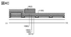
- 4A to 4C are diagrams for explaining the method for manufacturing the light emitting device according to the embodiment.
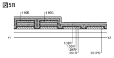
- 5A to 5C are diagrams for explaining the method for manufacturing the light emitting device according to the embodiment.
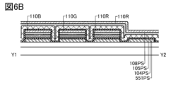
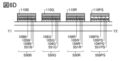
- 6A to 6D are diagrams for explaining the method for manufacturing the light emitting device according to the embodiment.
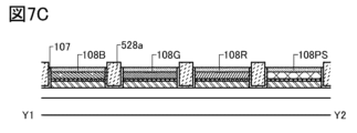
- 7A to 7D are diagrams illustrating the light emitting device according to the embodiment.
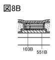
- 8A to 8C are diagrams illustrating the light emitting device according to the embodiment.
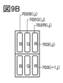
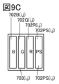
- FIG. 9A to 9F are diagrams for explaining the device and pixel arrangement according to the embodiment.
- 10A to 10C are diagrams illustrating pixel circuits according to embodiments.
- 11A and 11B are diagrams for explaining a light emitting device according to an embodiment.
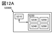
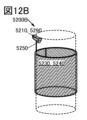
- FIG. 12A to 12E are diagrams illustrating electronic devices according to embodiments.
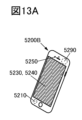
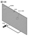
- 13A to 13E are diagrams illustrating electronic devices according to embodiments.
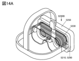
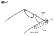
- 14A and 14B are diagrams for explaining the electronic device according to the embodiment.
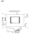
- 15A and 15B are diagrams illustrating the lighting device according to the embodiment.
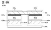
- FIGS. 18A and 18B are diagrams illustrating a light-emitting device and a light-receiving device according to an embodiment.
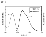
- FIG. 19 shows absorption and emission spectra of a dichloromethane solution of [Ce(bpz 3 ) 2 (bpz 2 )].
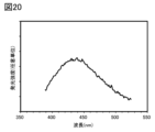
- FIG. 20 is an emission spectrum of a dichloromethane solution of [Ce(btaz 3 ) 2 (btaz 2 )].
- FIG. 21 is an emission spectrum of [Ce(btaz 3 ) 2 (btaz 2 )] powder.
- FIG. 22 is a diagram illustrating the configuration of the light emitting device 1.
- FIG. FIG. 23 is a diagram showing luminance-current density characteristics of the light-emitting device 1.
- FIG. 24 is a diagram showing the current efficiency-luminance characteristics of the light-emitting device 1.
- FIG. FIG. 25 is a diagram showing luminance-voltage characteristics of the light-emitting device 1.
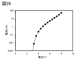
- FIG. 26 is a diagram showing current-voltage characteristics of the light-emitting device 1.
- FIG. 27 is a diagram showing the external quantum efficiency-luminance characteristics of the light-emitting device 1.
- FIG. 28 is a diagram showing the emission spectrum of the light emitting device 1.
- Display 1 A display using an organic EL element as a display element (organic EL display) has been put into practical use for a long time. Such displays typically have pixels that exhibit at least three colors of light, red, green, and blue, in order to achieve a full-color display.
- the pixel is provided with a light-emitting device for each emission color, and in a side-by-side display, a so-called separate-painting display, each light-emitting device has a different light-emitting substance according to the emission color of the corresponding pixel. are doing.
- Examples of light-emitting substances used in such light-emitting devices include a fluorescent light-emitting substance that emits light from a singlet excited state, a substance that emits thermally activated delayed fluorescence (TADF), and a substance that emits light from a triplet excited state.
- TADF thermally activated delayed fluorescence
- Phosphorescent substances and the like are mainly used and are being actively studied.
- the ratio of the singlet excited state to the triplet excited state is 1:3.
- the theoretical limit of internal quantum efficiency is known to be 25%.
- a phosphorescent substance can convert a singlet excited state to a triplet excited state by intersystem crossing, so that it can theoretically achieve an internal quantum efficiency of 100%, and a light-emitting device with high luminous efficiency can be obtained. can be done. Therefore, phosphorescent light-emitting materials are often used for red and green light-emitting devices in organic EL displays currently in practical use.
- the first factor is that the triplet state energy is lower than the singlet state energy in ordinary substances. Since blue light emission has high energy, a substance having a triplet excited level higher than that of the other two colors is required in order to obtain light emission from the triplet excited state. Naturally, the singlet excitation level of such a substance exists at a higher position, and a substance having such a level tends to be unstable. Moreover, when a host material is used, the host material needs to be a substance having a triplet excitation level and a singlet excitation level positioned at a higher energy level.
- the second factor is the length of the emission lifetime (also referred to as phosphorescence lifetime) of the phosphorescent substance. Since the transition from the triplet excited state to the singlet ground state is spin-forbidden and the transition from the singlet regular state to the singlet ground state is spin-allowed, phosphorescence has a much longer emission lifetime than fluorescence. (phosphorescence lifetime: ⁇ s, fluorescence lifetime: ⁇ ns). A long phosphorescence lifetime means a long lifetime of triplet excitons. Therefore, in a phosphorescent light-emitting device, the light-emitting substance remains in a high-energy excited state for a long time, which accelerates deterioration of the light-emitting substance itself or surrounding substances.
- the term excited state energy is higher than in the other two colors, so the effect of the exciton lifetime is even more pronounced than in the red and green phosphorescent devices, and the reliability for practical use is not expected. It is still difficult to obtain.
- the TADF material mentioned above is a kind of fluorescent substance because it emits light from a singlet excited state, but it enables reverse intersystem crossing. This makes it possible to convert triplet excitation energy into singlet excitation energy, and theoretically achieves an internal quantum efficiency of 100%, similar to phosphorescent materials. Therefore, a light-emitting device using a TADF material as a dopant and a light-emitting device using a TADF material as a host and a fluorescent light-emitting material as a dopant have been proposed, both of which have resulted in an internal quantum efficiency exceeding 25%.
- TADF materials have the same triplet excitation level problem as phosphorescent materials, and since reverse intersystem crossing is forbidden, TADF materials have long exciton lifetimes, making them as reliable as blue phosphorescent devices. It is currently difficult to secure
- organic complexes of Ce 3+ (4 f1 ) and Eu 2+ (4 f7 ) that emit light by fd transition which is a transition between f orbitals and d orbitals.
- Both the ground state and the excited state of these organic complexes are doublet states, and light is emitted from the doublet excited state.
- a singlet excited level and a triplet excited level are generated from the singlet ground state at a ratio of 1:3. Since both are doublet states, 100% of doublet excited states are theoretically generated without being restricted by the spin selection rule, and 100% internal quantum efficiency is possible.
- transitions between different orbitals are parity-forbidden, but fd transitions are parity-allowed transitions, so the transition speed is high and the exciton lifetime of the organic complexes described above is short.
- the transition speed is comparable to that of fluorescent light-emitting materials and is very fast.
- organic complexes of Ce 3+ (4 f1 ) and Eu 2+ (4 f7 ) that emit from the doublet excited state associated with the f–d transition are capable of 100% internal quantum efficiency and exciton It can be seen that it is a light-emitting substance that is expected to ensure high efficiency and high reliability in light-emitting devices because of its short life.
- one aspect of the present invention provides organic complexes of Ce 3+ with three borate ligands.
- the borate ligand has B - and a group that forms a covalent bond with B - .
- some or all of the groups forming a covalent bond with B ⁇ have lone pairs of electrons that can coordinate to Ce 3+ .
- a heteroaryl group having two or more nitrogen atoms can be used, specifically, either one or both of a pyrazolyl group and a triazolyl group. can be mentioned.
- a borate ligand can be coordinated to Ce 3+ by donating a lone pair of electrons possessed by the nitrogen atom of the pyrazolyl or triazolyl group.
- the total number of pyrazolyl groups and triazolyl groups forming a covalent bond with B- is excessive, the molecular weight of the entire organic complex may increase and the sublimability of the organic complex may deteriorate. Therefore, by synthesizing a borate ligand in which the number of pyrazolyl groups and triazolyl groups is controlled to the target number and coordinating the borate ligand to Ce 3+ , the total number of pyrazolyl groups and triazolyl groups in the entire organic complex is It is preferable to adjust the number of
- the coordination number to Ce 3+ is preferably 7 or more and 9 or less, more preferably 8. Therefore, the total number of pyrazolyl groups and triazolyl groups in the organic complex is preferably 7 or more and 9 or less, more preferably 8.
- the total number of pyrazolyl groups and triazolyl groups in this way an organic complex that is stable and highly sublimable can be provided. Therefore, it is suitable as a light-emitting material for light-emitting devices.
- One or more of the pyrazolyl group and triazolyl group of the borate ligand may be bonded to an alkyl group, a cycloalkyl group, or an aryl group.
- steric hindrance can be controlled and the bond distance between the borate ligand and Ce 3+ can be changed, making it possible to adjust the emission color. Further, by changing the types of these substituents, improvement in reliability can be expected.
- an alkyl group, a cycloalkyl group or an aryl group may be bonded to B- .
- steric hindrance can be controlled and the bond distance between the borate ligand and Ce 3+ can be changed, making it possible to adjust the emission color.
- improvement in reliability of the organometallic complex can be expected.
- one embodiment of the present invention is an organometallic complex represented by General Formula (G1).
- X represents carbon or nitrogen, where the carbon is hydrogen (including deuterium), a substituted or unsubstituted alkyl group having 1 to 10 carbon atoms, or a substituted or unsubstituted 3 to 10 carbon atoms or a substituted or unsubstituted aryl group having 6 to 30 carbon atoms.
- R 1 to R 3 are each independently hydrogen (including deuterium), a substituted or unsubstituted alkyl group having 1 to 10 carbon atoms, a substituted or unsubstituted cycloalkyl group having 3 to 10 carbon atoms, and a substituted or any one of unsubstituted aryl groups having 6 to 30 carbon atoms.
- n represents an integer of 1 or more and 4 or less.
- each borate ligand may be the same or different.
- n of each borate ligand may be the same or different.
- X of each borate ligand may be the same or different, and R 1 of each borate ligand may be the same or different.
- R2 of each borate ligand may be the same or different from each other.
- R 3 of each borate ligand may be the same or different.
- Another embodiment of the present invention is an organometallic complex represented by General Formula (G2).
- R 1 to R 3 are each independently hydrogen (including deuterium), a substituted or unsubstituted alkyl group having 1 to 10 carbon atoms, a substituted or unsubstituted cyclo represents any one of an alkyl group and a substituted or unsubstituted aryl group having 6 to 30 carbon atoms; Moreover, n represents an integer of 1 or more and 4 or less.
- each borate ligand may be the same or different.
- n of each borate ligand may be the same or different.
- X of each borate ligand may be the same or different
- R 1 of each borate ligand may be the same or different.
- R2 of each borate ligand may be the same or different from each other.
- R 3 of each borate ligand may be the same or different.
- a Ce 3+ organic complex having a borate ligand having a triazolyl group may reduce the ligand field splitting, so the molar extinction coefficient can be increased.
- the total number of pyrazolyl groups and triazolyl groups in the Ce 3+ organic complex is preferably 7 or more and 9 or less, more preferably 8. Therefore, in general formulas (G1) and (G2), the sum of three n's is preferably 7 or more and 9 or less, more preferably 8.
- Another embodiment of the present invention is an organometallic complex represented by General Formula (G3).
- X 1 to X 3 each independently represent carbon or nitrogen, and the carbons are each independently hydrogen (including deuterium) or a substituted or unsubstituted alkyl group having 1 to 10 carbon atoms , a substituted or unsubstituted cycloalkyl group having 3 to 10 carbon atoms, or a substituted or unsubstituted aryl group having 6 to 30 carbon atoms.
- R 11 to R 13 , R 21 to R 23 and R 31 to R 33 are each independently hydrogen (including deuterium), substituted or unsubstituted alkyl group having 1 to 10 carbon atoms, substituted or unsubstituted represents any one of a cycloalkyl group having 3 to 10 carbon atoms and a substituted or unsubstituted aryl group having 6 to 30 carbon atoms.
- j, k, and p each independently represents an integer of 1 or more and 4 or less. When j is 2 or more, each X 1 may be the same or different, each R 11 may be the same or different, and each R 12 may be They may be the same or different.
- each X2 may be the same or different, each R21 may be the same or different, and each R22 may be They may be the same or different.
- each X 3 may be the same or different, each R 31 may be the same or different, and each R 32 may be They may be the same or different.
- each R 13 may be the same or different.
- each R 23 may be the same or different.
- each R 33 may be the same or different.
- Another embodiment of the present invention is an organometallic complex represented by General Formula (G3′).
- X 1 to X 3 each independently represent carbon or nitrogen, and the carbons are each independently hydrogen (including deuterium), substituted or unsubstituted alkyl having 1 to 10 carbon atoms group, a substituted or unsubstituted C3-C10 cycloalkyl group, or a substituted or unsubstituted C6-C30 aryl group.
- R 11 to R 13 , R 21 to R 23 and R 31 to R 33 are each independently hydrogen (including deuterium), substituted or unsubstituted alkyl group having 1 to 10 carbon atoms, substituted or unsubstituted represents any one of a cycloalkyl group having 3 to 10 carbon atoms and a substituted or unsubstituted aryl group having 6 to 30 carbon atoms.
- j represents an integer of 1 or more and 3 or less.
- k and p each independently represents an integer of 1 or more and 4 or less.
- each X 1 may be the same or different
- each R 11 may be the same or different
- each R 12 may be They may be the same or different.
- each X2 may be the same or different, each R21 may be the same or different, and each R22 may be They may be the same or different.
- each X 3 may be the same or different, each R 31 may be the same or different, and each R 32 may be They may be the same or different.
- each R 13 may be the same or different.
- each R 23 may be the same or different.
- each R 33 may be the same or different.
- Another embodiment of the present invention is an organometallic complex represented by General Formula (G4).
- X 2 and X 3 each independently represent carbon or nitrogen, and the carbons are each independently hydrogen (including deuterium) or a substituted or unsubstituted alkyl group having 1 to 10 carbon atoms , a substituted or unsubstituted cycloalkyl group having 3 to 10 carbon atoms, or a substituted or unsubstituted aryl group having 6 to 30 carbon atoms.
- R 11 to R 13 , R 21 to R 23 and R 31 to R 33 are each independently hydrogen (including deuterium), substituted or unsubstituted alkyl group having 1 to 10 carbon atoms, substituted or unsubstituted represents any one of a cycloalkyl group having 3 to 10 carbon atoms and a substituted or unsubstituted aryl group having 6 to 30 carbon atoms.
- j, k, and p each independently represents an integer of 1 or more and 4 or less. When j is 2 or more, each R 11 may be the same or different, and each R 12 may be the same or different.
- each X2 may be the same or different, each R21 may be the same or different, and each R22 may be They may be the same or different.
- each X 3 may be the same or different, each R 31 may be the same or different, and each R 32 may be They may be the same or different.
- each R 13 may be the same or different.
- each R 23 may be the same or different.
- each R 33 may be the same or different.
- a Ce 3+ organic complex having a borate ligand having at least one triazolyl group such as the organometallic complex represented by the general formula (G4), may reduce the ligand field splitting. Therefore, the molar extinction coefficient can be increased.
- the total number of pyrazolyl groups and triazolyl groups in the Ce 3+ organic complex is preferably 7 or more and 9 or less, more preferably 8. Therefore, in general formulas (G3), (G3′) and (G4), the sum of j, k and p is preferably 7 or more and 9 or less, more preferably 8.
- Another embodiment of the present invention is an organometallic complex represented by General Formula (G5).
- X 11 to X 13 , X 21 to X 23 , X 31 and X 32 each independently represent carbon or nitrogen, and the carbons are each independently hydrogen (including deuterium), substituted or any one of an unsubstituted alkyl group having 1 to 10 carbon atoms, a substituted or unsubstituted cycloalkyl group having 3 to 10 carbon atoms, and a substituted or unsubstituted aryl group having 6 to 30 carbon atoms.
- R 41 to R 47 , R 51 to R 57 and R 61 to R 66 are each independently hydrogen (including deuterium), substituted or unsubstituted alkyl group having 1 to 10 carbon atoms, substituted or unsubstituted represents any one of a cycloalkyl group having 3 to 10 carbon atoms and a substituted or unsubstituted aryl group having 6 to 30 carbon atoms.
- the coordination number of Ce 3+ can be eight, which is preferable. With such a structure, an organometallic complex that is stable and highly sublimable can be obtained. Therefore, the organometallic complex can be used as a light-emitting material suitable for a light-emitting device.
- alkyl groups having 1 to 10 carbon atoms include methyl group, ethyl group, propyl group, isopropyl group, butyl group, sec-butyl group and isobutyl group.
- tert-butyl group pentyl group, isopentyl group, sec-pentyl group, tert-pentyl group, neopentyl group, hexyl group, isohexyl group, sec-hexyl group, tert-hexyl group, neohexyl group, 3-methylpentyl group, 2-methylpentyl group, 2-ethylbutyl group, 1,2-dimethylbutyl group, 2,3-dimethylbutyl group and the like.
- the substituent is an alkyl group having 1 to 4 carbon atoms, a cycloalkyl group having 3 to 6 carbon atoms, or an aryl group having 6 to 13 carbon atoms.
- cycloalkyl group having 3 to 10 carbon atoms include a cyclopropyl group, a cyclobutyl group, a methylcyclobutyl group, a cyclopentyl group, a methylcyclopentyl group, and an isopropylcyclopentyl group.
- the substituent is an alkyl group having 1 to 4 carbon atoms, a cycloalkyl group having 3 to 6 carbon atoms, or an aryl group having 6 to 13 carbon atoms. based on.
- the aryl group having 6 to 30 carbon atoms includes a phenyl group, an o-tolyl group, an m-tolyl group, a p-tolyl group, a mesityl group, and an o-biphenyl group.
- aryl group having 6 to 30 carbon atoms has a substituent, the substituent is an alkyl group having 1 to 4 carbon atoms, a cycloalkyl group having 3 to 6 carbon atoms, or an aryl group having 6 to 13 carbon atoms.
- the steric hindrance in the organometallic complex can be controlled, and the bond distance between the borate ligand and Ce 3+ can be changed, making it possible to adjust the emission color. Further, by introducing these substituents, improvement in reliability of the organometallic complex can be expected. For example, by introducing a methyl group, moderate steric hindrance can be obtained, so that the reliability of the organometallic complex can be improved.
- organometallic complexes of one embodiment of the present invention and the organometallic complexes that can be used for a light-emitting device, which have structures represented by any of the above general formulas (G1) to (G5), are given below. shown in
- organometallic complexes represented by the structural formulas (100) to (179) are specific examples of the structures represented by the general formulas (G1) to (G5), and are one embodiment of the present invention. is not limited to this.
- X represents carbon or nitrogen, where the carbon is hydrogen (including deuterium), a substituted or unsubstituted alkyl group having 1 to 10 carbon atoms, or a substituted or unsubstituted 3 to 10 carbon atoms or a substituted or unsubstituted aryl group having 6 to 30 carbon atoms.
- R 1 to R 3 are each independently hydrogen (including deuterium), a substituted or unsubstituted alkyl group having 1 to 10 carbon atoms, a substituted or unsubstituted cycloalkyl group having 3 to 10 carbon atoms, and a substituted or any one of unsubstituted aryl groups having 6 to 30 carbon atoms.
- n represents an integer of 1 or more and 4 or less.
- each borate ligand may be the same or different.
- n of each borate ligand may be the same or different.
- X of each borate ligand may be the same or different, and R 1 of each borate ligand may be the same or different.
- R2 of each borate ligand may be the same or different from each other.
- R 3 of each borate ligand may be the same or different.
- the organometallic complex of one embodiment of the present invention represented by General Formula (G1) has a heteroaromatic ring represented by General Formula (g1), as shown in Synthesis Scheme (A-1) below.
- a cerium compound a trivalent cerium salt such as cerium(III) chloride, cerium(III) nitrate, and cerium(III) trifluoromethanesulfonate
- one organic solvent such as an alcoholic solvent, tetrahydrofuran, or chloroform
- Organometallic complexes represented by other general formulas can also be synthesized in the same manner as described above.
- Embodiment 2 In this embodiment mode, a structure of a light-emitting device in which a material that emits light from a doublet excited state is used as a light-emitting substance for a light-emitting layer will be described with reference to FIGS. 1A to 1E.
- the light-emitting substance is not particularly limited as long as it emits light from a doublet excited state; however, the organometallic complex described in Embodiment 1 is preferably used.
- FIG. 1A shows a light-emitting device having an EL layer that includes a light-emitting layer between a pair of electrodes. Specifically, it has a structure in which an EL layer 103 is sandwiched between a first electrode 101 and a second electrode 102 .
- FIG. 1B shows a laminated structure (tandem structure) having a plurality of (two layers in FIG. 1B) EL layers (103a and 103b) between a pair of electrodes and a charge generation layer 106 between the EL layers. of the light emitting device.
- a light-emitting device with a tandem structure can realize a highly efficient light-emitting device without changing the amount of current.
- the charge generation layer 106 injects electrons into one EL layer (103a or 103b) and injects electrons into the other EL layer (103b or 103a) has a function of injecting holes. Therefore, in FIG. 1B, when a voltage is applied to the first electrode 101 so that the potential is higher than that of the second electrode 102, electrons are injected from the charge generation layer 106 into the EL layer 103a, and the EL layer 103b is positively charged. A hole is to be injected.
- the charge generation layer 106 may have a property of transmitting visible light (specifically, the visible light transmittance of the charge generation layer 106 is 40% or more). preferable. Also, the charge generation layer 106 functions even with a lower conductivity than the first electrode 101 and the second electrode 102 .
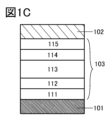
- FIG. 1C shows a layered structure of the EL layer 103 of the light-emitting device which is one embodiment of the present invention.
- the first electrode 101 functions as an anode and the second electrode 102 functions as a cathode.
- the EL layer 103 has a structure in which a hole-injection layer 111, a hole-transport layer 112, a light-emitting layer 113, an electron-transport layer 114, and an electron-injection layer 115 are sequentially stacked over the first electrode 101.
- the light-emitting layer 113 may have a structure in which a plurality of light-emitting layers emitting light of different colors are stacked.
- a light-emitting layer containing a light-emitting substance that emits red light, a light-emitting layer that contains a light-emitting substance that emits green light, and a light-emitting layer that contains a light-emitting substance that emits blue light are stacked, or a layer containing a carrier-transporting material is interposed therebetween. It may be a laminated structure. Alternatively, a light-emitting layer containing a light-emitting substance that emits yellow light and a light-emitting layer containing a light-emitting substance that emits blue light may be combined. However, the laminated structure of the light-emitting layer 113 is not limited to the above.
- the light-emitting layer 113 may have a structure in which a plurality of light-emitting layers emitting light of the same color are stacked.
- a structure in which a first light-emitting layer containing a light-emitting substance that emits blue light and a second light-emitting layer containing a light-emitting substance that emits blue light are stacked or stacked with a layer containing a carrier-transporting material interposed therebetween. It can be.
- reliability may be improved as compared with a single-layer structure.
- each EL layer is stacked sequentially from the anode side as described above.
- the stacking order of the EL layers 103 is reversed.
- 111 on the first electrode 101 which is a cathode is an electron injection layer
- 112 is an electron transport layer
- 113 is a light emitting layer
- 114 is a hole transport layer
- 115 is a hole. It has a configuration of an injection layer.
- the light-emitting layer 113 included in the EL layers (103, 103a, 103b) has an appropriate combination of a plurality of substances including a material that emits light from a doublet excited state.
- a structure in which different emission colors are obtained from the plurality of EL layers (103a and 103b) shown in FIG. 1B may be employed.
- different materials may be used for the light-emitting substance and other substances used in each light-emitting layer.
- the light-emitting device which is one embodiment of the present invention, for example, the first electrode 101 shown in FIG. ) structure
- light emitted from the light emitting layer 113 included in the EL layer 103 can be resonated between the two electrodes, and light emitted from the second electrode 102 can be enhanced.
- the film of the transparent conductive film Optical tuning can be achieved by controlling the thickness. Specifically, the optical distance between the first electrode 101 and the second electrode 102 (the product of the film thickness and the refractive index) is m ⁇ / It is preferable to adjust to 2 (where m is an integer equal to or greater than 1) or its vicinity.
- the optical distance from the first electrode 101 to the region (light-emitting region) of the light-emitting layer 113 from which desired light is obtained (2m′+1) ⁇ /4 (where m′ is an integer equal to or greater than 1) or the vicinity thereof. It is preferable to adjust so that Note that the light-emitting region here means a recombination region of holes and electrons in the light-emitting layer 113 .
- the spectrum of specific monochromatic light obtained from the light-emitting layer 113 can be narrowed, and light emission with good color purity can be obtained.
- the optical distance between the first electrode 101 and the second electrode 102 is the total thickness from the reflection area of the first electrode 101 to the reflection area of the second electrode 102. can.
- the optical distance between the first electrode 101 and the light-emitting layer from which desired light is obtained is the optical distance between the reflection region in the first electrode 101 and the light-emitting region in the light-emitting layer from which desired light is obtained. It can be said that it is the distance.
- an arbitrary position of the first electrode 101 can be set as the reflective region and the desired light.
- an arbitrary position of the light-emitting layer from which light is obtained is the light-emitting region, the above effects can be sufficiently obtained.
- the light-emitting device shown in FIG. 1D is a light-emitting device having a tandem structure and has a microcavity structure, so that light of different wavelengths (monochromatic light) can be extracted from each EL layer (103a, 103b). Therefore, separate coloring (for example, RGB) for obtaining different emission colors is unnecessary. Therefore, it is easy to achieve high definition. A combination with a colored layer (color filter) is also possible. Furthermore, since it is possible to increase the emission intensity of the specific wavelength in the front direction, it is possible to reduce power consumption.
- the light-emitting device shown in FIG. 1E is an example of the tandem structure light-emitting device shown in FIG. It has a structure in which it is sandwiched and laminated.
- the three EL layers (103a, 103b, 103c) each have a light-emitting layer (113a, 113b, 113c), and the emission colors of the respective light-emitting layers can be freely combined.
- light-emitting layer 113a can be blue
- light-emitting layer 113b can be either red, green, or yellow
- light-emitting layer 113c can be blue
- light-emitting layer 113a can be red and light-emitting layer 113b can be blue, green, or yellow.
- the light-emitting layer 113c may be red.
- the first electrode 101 and the second electrode 102 is a light-transmitting electrode (a transparent electrode, a semi-transmissive/semi-reflective electrode, or the like). do.
- the visible light transmittance of the transparent electrode is set to 40% or more.
- the visible light reflectance of the semi-transmissive/semi-reflective electrode should be 20% or more and 80% or less, preferably 40% or more and 70% or less.
- these electrodes preferably have a resistivity of 1 ⁇ 10 ⁇ 2 ⁇ cm or less.
- the reflective electrode when one of the first electrode 101 and the second electrode 102 is a reflective electrode (reflective electrode), the reflective electrode The light reflectance is 40% or more and 100% or less, preferably 70% or more and 100% or less. Moreover, the electrode preferably has a resistivity of 1 ⁇ 10 ⁇ 2 ⁇ cm or less.
- FIG. 1D having a tandem structure.
- the structure of the EL layer is the same for the single-structure light-emitting device shown in FIGS. 1A and 1C.
- the first electrode 101 is formed as a reflective electrode
- the second electrode 102 is formed as a semi-transmissive/semi-reflective electrode. Therefore, a desired electrode material can be used singly or plurally to form a single layer or lamination.
- the second electrode 102 is formed by selecting an appropriate material after the EL layer 103b is formed.
- First electrode and second electrode> As materials for forming the first electrode 101 and the second electrode 102, the following materials can be used in appropriate combination as long as the above-described functions of both electrodes can be satisfied. For example, metals, alloys, electrically conductive compounds, mixtures thereof, and the like can be used as appropriate. Specifically, In--Sn oxide (also referred to as ITO), In--Si--Sn oxide (also referred to as ITSO), In--Zn oxide, and In--W--Zn oxide are given.
- ITO In--Sn oxide
- ITSO In--Si--Sn oxide
- ITSO In--Zn oxide
- In--W--Zn oxide In--W--Zn oxide
- elements belonging to Group 1 or Group 2 of the periodic table of elements not exemplified above e.g., lithium (Li), cesium (Cs), calcium (Ca), strontium (Sr)), europium (Eu), ytterbium Rare earth metals such as (Yb), alloys containing an appropriate combination thereof, graphene, and the like can be used.
- a hole injection layer 111a and a hole transport layer 112a of the EL layer 103a are sequentially stacked on the first electrode 101 by vacuum deposition. be.
- hole injection layer 111b and hole transport layer 112b of EL layer 103b are sequentially laminated on charge generation layer 106 in the same manner.
- the hole injection layers (111, 111a, 111b) inject holes from the first electrode 101, which is an anode, and the charge generation layers (106, 106a, 106b) into the EL layers (103, 103a, 103b). It is a layer containing an organic acceptor material and a material with a high hole injection property.
- the organic acceptor material has a LUMO (Lowest Unoccupied Molecular Orbital) level value and a HOMO (Highest Occupied Molecular Orbital) level value close to other organic compounds. It is a material that can generate holes in the organic compound by causing the organic compound to generate holes. Therefore, compounds having electron-withdrawing groups (halogen groups or cyano groups) such as quinodimethane derivatives, chloranil derivatives, and hexaazatriphenylene derivatives can be used as organic acceptor materials.
- halogen groups or cyano groups such as quinodimethane derivatives, chloranil derivatives, and hexaazatriphenylene derivatives
- a compound in which an electron-withdrawing group is bound to a condensed aromatic ring having a plurality of heteroatoms such as HAT-CN, is suitable because it has a high acceptor property and stable film quality against heat.
- [3] radialene derivatives having an electron-withdrawing group are preferred because of their extremely high electron-accepting properties, specifically ⁇ , ⁇ ', ⁇ '.
- Materials with high hole injection properties include oxides of metals belonging to groups 4 to 8 in the periodic table (molybdenum oxide, vanadium oxide, ruthenium oxide, tungsten oxide, manganese oxide, etc.). transition metal oxides, etc.) can be used. Specific examples include molybdenum oxide, vanadium oxide, niobium oxide, tantalum oxide, chromium oxide, tungsten oxide, manganese oxide, and rhenium oxide. Among the above, molybdenum oxide is preferred because it is stable in the atmosphere, has low hygroscopicity, and is easy to handle. In addition, a phthalocyanine-based compound such as phthalocyanine (abbreviation: H 2 Pc) or copper phthalocyanine (abbreviation: CuPc) can be used.
- H 2 Pc phthalocyanine
- CuPc copper phthalocyanine
- low-molecular-weight compounds such as 4,4′,4′′-tris(N,N-diphenylamino)triphenylamine (abbreviation: TDATA) and 4,4′,4′′-tris [N-(3-methylphenyl)-N-phenylamino]triphenylamine (abbreviation: MTDATA), 4,4′-bis[N-(4-diphenylaminophenyl)-N-phenylamino]biphenyl (abbreviation: DPAB), N,N′-bis[4-bis(3-methylphenyl)aminophenyl]-N,N′-diphenyl-4,4′-diaminobiphenyl (abbreviation: DNTPD), 1,3,5-tris [N-(4-diphenylaminophenyl)-N-phenylamino]benzene (abbreviation: DPA3B), 3-[N-(9-phenyl
- poly(N-vinylcarbazole) (abbreviation: PVK)
- poly(4-vinyltriphenylamine) (abbreviation: PVTPA)
- PVTPA poly(4-vinyltriphenylamine)
- PTPDMA poly[N-(4 - ⁇ N'-[4-(4-diphenylamino)phenyl]phenyl-N'-phenylamino ⁇ phenyl)methacrylamide]
- PTPDMA poly[N,N'-bis(4-butylphenyl)- N,N'-bis(phenyl)benzidine]
- Poly-TPD poly(N-vinylcarbazole) or the like
- PEDOT/PSS poly(3,4-ethylenedioxythiophene)/polystyrene sulfonic acid
- PAni/PSS polyaniline/polystyrene sulfonic acid
- other acid-added polymer compounds etc.
- a mixed material containing a hole-transporting material and the above-described organic acceptor material can also be used.
- electrons are extracted from the hole-transporting material by the organic acceptor material, holes are generated in the hole-injection layer 111 , and holes are injected into the light-emitting layer 113 via the hole-transporting layer 112 .
- the hole injection layer 111 may be formed of a single layer made of a mixed material containing a hole-transporting material and an organic acceptor material (electron-accepting material). (electron-accepting material) may be laminated in separate layers.
- the hole-transporting material a substance having a hole mobility of 1 ⁇ 10 ⁇ 6 cm 2 /Vs or more at a square root of an electric field strength [V/cm] of 600 is preferable. Note that any substance other than these can be used as long as it has a higher hole-transport property than electron-transport property.
- hole-transporting materials include compounds having a ⁇ -electron-rich heteroaromatic ring (e.g., carbazole derivatives, furan derivatives, or thiophene derivatives), and positive compounds such as aromatic amines (organic compounds having an aromatic amine skeleton). Materials with high pore transport properties are preferred.
- carbazole derivatives organic compounds having a carbazole ring
- examples of the carbazole derivatives include bicarbazole derivatives (eg, 3,3'-bicarbazole derivatives) and aromatic amines having a carbazolyl group.
- bicarbazole derivative for example, 3,3′-bicarbazole derivative
- PCCP 3,3′-bis(9-phenyl-9H-carbazole)
- BisBPCz 9,9 '-bis(biphenyl-4-yl)-3,3'-bi-9H-carbazole
- BismBPCz 9,9'-bis(1,1'-biphenyl-3-yl)-3,3' -bi-9H-carbazole
- BismBPCz 9-(1,1′-biphenyl-3-yl)-9′-(1,1′-biphenyl-4-yl)-9H,9′H-3 ,3′-bicarbazole
- mBPCCBP 9,2-naphthyl)-9′-phenyl-9H,9′H-3,3′-bicarbazole
- ⁇ NCCP 9-(2-naphthyl)-9′-phenyl-9H,9′H-3,3′-bicarbazol
- aromatic amine having a carbazolyl group examples include 4-phenyl-4′-(9-phenyl-9H-carbazol-3-yl)triphenylamine (abbreviation: PCBA1BP), N-( 4-biphenyl)-N-(9,9-dimethyl-9H-fluoren-2-yl)-9-phenyl-9H-carbazol-3-amine (abbreviation: PCBiF), N-(biphenyl-4-yl)- N-[4-(9-phenyl-9H-carbazol-3-yl)phenyl]-9,9-dimethyl-9H-fluoren-2-amine (abbreviation: PCBBiF), N-[4-(9-phenyl- 9H-carbazol-3-yl)phenyl]-bis(9,9-dimethyl-9H-fluoren-2-yl)amine (abbreviation: PCBFF), N-(1,1′-biphenyl-4-
- PCPPn 9-[4-(9-phenyl-9H-carbazol-3-yl)-phenyl]phenanthrene
- PCPN 3-[4-(1-naphthyl) -Phenyl]-9-phenyl-9H-carbazole
- mCP 1,3-bis(N-carbazolyl)benzene
- CBP 4,4′-di(N-carbazolyl)biphenyl
- CzTP 3,6-bis(3,5-diphenylphenyl)-9-phenylcarbazole
- TCPB 9-[4-(10-phenyl-9-anthracenyl)phenyl]-9H-carbazole
- furan derivative organic compound having a furan ring
- DBF3P- II 4,4′,4′′-(benzene-1,3,5-triyl)tri(dibenzofuran)
- mmDBFFLBi-II 4- ⁇ 3-[3-(9-phenyl-9H-fluoren-9-yl)phenyl]phenyl ⁇ dibenzofuran
- thiophene derivative an organic compound having a thiophene ring
- DBT3P 4,4′,4′′-(benzene-1,3,5-triyl)tri(dibenzothiophene)
- DBT3P 4,4′,4′′-(benzene-1,3,5-triyl)tri(dibenzothiophene)
- DBTFLP-III 2,8-diphenyl-4-[4-(9-phenyl-9H-fluoren-9-yl)phenyl]dibenzothiophene
- DBTFLP-III 4-[4-(9-phenyl- 9H-fluoren-9-yl)phenyl]-6-phenyldibenzothiophene
- DBTFLP-IV 4-[4-(9-phenyl- 9H-fluoren-9-yl)phenyl]-6-phenyldibenzothiophene
- aromatic amine examples include 4,4′-bis[N-(1-naphthyl)-N-phenylamino]biphenyl (abbreviation: NPB or ⁇ -NPD), N,N′- Diphenyl-N,N'-bis(3-methylphenyl)-4,4'-diaminobiphenyl (abbreviation: TPD), N,N'-bis(9,9'-spirobi[9H-fluoren]-2-yl )-N,N′-diphenyl-4,4′-diaminobiphenyl (abbreviation: BSPB), 4-phenyl-4′-(9-phenylfluoren-9-yl)triphenylamine (abbreviation: BPAFLP), 4- Phenyl-3′-(9-phenylfluoren-9-yl)triphenylamine (abbreviation: mBPAFLP), N-(9,9-dimethyl-9H-
- PVK poly(N-vinylcarbazole)
- PVK poly(4-vinyltriphenylamine)
- PVK high molecular compounds
- PVTPA poly[N-(4- ⁇ N'-[4-(4-diphenylamino)phenyl]phenyl-N'-phenylamino ⁇ phenyl)methacrylamide]
- PTPDMA poly[N,N' -Bis(4-butylphenyl)-N,N'-bis(phenyl)benzidine]
- Poly-TPD poly[N,N' -Bis(4-butylphenyl)-N,N'-bis(phenyl)benzidine]
- PEDOT/PSS poly(3,4-ethylenedioxythiophene)/polystyrene sulfonic acid
- PAni/PSS polyaniline/polystyrene sulfonic acid
- other acid-added polymer compounds etc.
- the hole-transporting material is not limited to the above, and one or a combination of various known materials may be used as the hole-transporting material.
- the hole injection layers (111, 111a, 111b) can be formed using various known film forming methods, and for example, can be formed using a vacuum deposition method.
- the hole transport layers (112, 112a, 112b) transfer holes injected from the first electrode 101 to the light emitting layers (113, 113a, 113b, 113c) by the hole injection layers (111, 111a, 111b). This is the transport layer.
- the hole-transporting layers (112, 112a, 112b) are layers containing a hole-transporting material. Therefore, for the hole transport layers (112, 112a, 112b), a hole transport material that can be used for the hole injection layers (111, 111a, 111b) can be used.
- the same organic compound as that for the hole-transport layers (112, 112a, and 112b) can be used for the light-emitting layers (113, 113a, 113b, and 113c).
- the hole transport layers (112, 112a, 112b) and the light emitting layers (113, 113a, 113b, 113c) can be efficiently transported, which is more preferable.
- the light-emitting layers (113, 113a, 113b, 113c) are layers containing light-emitting substances.
- a material that emits light from a doublet excited state can be used as the light-emitting substance.
- the light-emitting substance is not particularly limited as long as it emits light from a doublet excited state; however, the organometallic complex described in Embodiment 1 is preferably used.
- the light-emitting layers (113, 113a, 113b, 113c) may contain one or more organic compounds (host material, etc.) in addition to the light-emitting substance (guest material).
- organic compound used as the host material a hole-transporting material that can be used in the hole-transporting layers (112, 112a, 112b) described above, or a hole-transporting material that can be used in the above-described hole-transporting layers (112, 112a, 112b) as long as it satisfies the conditions as a host material used in the light-emitting layer.
- organic compounds such as electron-transporting materials that can be used for the electron-transporting layers (114, 114a, 114b) of .
- the present inventors have found that when a material that emits light from a doublet excited state is used as a light-emitting substance in the light-emitting layer, the host material preferably contains an electron-transporting heteroaromatic compound. Considering the carrier-transporting properties of the doublet light-emitting material, the host material preferably transports electrons, and the heteroaromatic ring is stable as the electron-transporting skeleton. As the electron-transporting heteroaromatic compound used as the host material, a ⁇ -electron-deficient heteroaromatic compound is preferably used. Note that the light-emitting substance in this case is not particularly limited as long as it emits light from a doublet excited state; however, the organometallic complex described in Embodiment 1 is preferable.
- ⁇ -electron-deficient heteroaromatic compounds include, for example, phenanthroline derivatives, quinoline derivatives, benzoquinoline derivatives, quinoxaline derivatives, dibenzoquinoxaline derivatives, pyridine derivatives, bipyridine derivatives, diazine (pyrimidine, pyrazine, pyridazine) derivatives, Compounds containing nitrogen-containing six-membered heteroaromatic rings, such as triazine derivatives, can be mentioned.
- the heteroaromatic ring of these derivatives may be further condensed with an aromatic ring such as a benzene ring.
- ⁇ -electron-deficient heteroaromatic compound examples include a ⁇ -electron-deficient heteroaromatic compound can be obtained from an organic compound such as the above-described hole-transporting material or the below-described electron-transporting material. can be selected.
- the electron transport layers (114, 114a, 114b) transfer electrons injected from the second electrode 102 and the charge generation layers (106, 106a, 106b) by the electron injection layers (115, 115a, 115b) described later into the light emitting layer ( 113, 113a, 113b, 113c).
- the heat resistance of the light-emitting device which is one embodiment of the present invention, can be improved when the electron-transport layer has a layered structure.
- the electron transporting material used for the electron transporting layers (114, 114a, 114b) has an electron mobility of 1 ⁇ 10 ⁇ 6 cm 2 /Vs or more when the square root of the electric field strength [V/cm] is 600.
- a substance with a degree of hardness is preferred. Note that any substance other than these substances can be used as long as it has a higher electron-transport property than hole-transport property.
- the electron transport layers (114, 114a, 114b) function as a single layer, but may have a laminated structure of two or more layers. Since the above mixed material has heat resistance, the effect of the heat process on the device characteristics can be suppressed by performing a photolithography process on the electron transport layer using the mixed material.
- an organic compound having a high electron-transporting property can be used, and for example, a heteroaromatic compound can be used.
- a heteroaromatic compound is a cyclic compound containing at least two different elements in the ring.
- the ring structure includes a 3-membered ring, a 4-membered ring, a 5-membered ring, a 6-membered ring, etc., and a 5-membered ring or a 6-membered ring is particularly preferable.
- Heteroaromatic compounds containing any one or more of nitrogen, oxygen, or sulfur are preferred.
- nitrogen-containing heteroaromatic compounds nitrogen-containing heteroaromatic compounds
- materials with high electron transport properties such as nitrogen-containing heteroaromatic compounds or ⁇ -electron deficient heteroaromatic compounds containing these (electron transport properties material) is preferably used.
- a material different from the material used for the light-emitting layer can also be used for this electron-transporting material. Not all excitons generated by recombination of carriers in the light-emitting layer can contribute to light emission, and may diffuse into layers in contact with or in the vicinity of the light-emitting layer. In order to avoid this phenomenon, the electron transport material is preferably different from the material used for the light-emitting layer. This makes it possible to obtain a highly efficient device.
- a heteroaromatic compound is an organic compound having at least one heteroaromatic ring.
- the heteroaromatic ring has any one of a pyridine ring, a diazine ring, a triazine ring, a polyazole ring, an oxazole ring, a thiazole ring, and the like.
- heteroaromatic rings having a diazine ring include heteroaromatic rings having a pyrimidine ring, a pyrazine ring, a pyridazine ring, or the like.
- heteroaromatic rings having a polyazole ring include heteroaromatic rings having an imidazole ring, a triazole ring, and an oxadiazole ring.
- a heteroaromatic ring also includes a fused heteroaromatic ring having a fused ring structure.
- the condensed heteroaromatic ring includes quinoline ring, benzoquinoline ring, quinoxaline ring, dibenzoquinoxaline ring, quinazoline ring, benzoquinazoline ring, dibenzoquinazoline ring, phenanthroline ring, furodiazine ring, and benzimidazole ring.
- heteroaromatic compounds having a 5-membered ring structure include heteroaromatic compounds having an imidazole ring compounds, heteroaromatic compounds having a triazole ring, heteroaromatic compounds having an oxazole ring, heteroaromatic compounds having an oxadiazole ring, heteroaromatic compounds having a thiazole ring, heteroaromatic compounds having a benzimidazole ring, etc. is mentioned.
- heteroaromatic compounds having a 6-membered ring structure include a pyridine ring, a diazine ring (pyrimidine ring, pyrazine ring, pyridazine ring, etc.), heteroaromatic compounds having heteroaromatic rings such as triazine ring and polyazole ring. It is included in heteroaromatic compounds having a structure in which pyridine rings are linked, and includes heteroaromatic compounds having a bipyridine structure and heteroaromatic compounds having a terpyridine structure.
- the heteroaromatic compound having a condensed ring structure partially including the six-membered ring structure includes a quinoline ring, a benzoquinoline ring, a quinoxaline ring, a dibenzoquinoxaline ring, a phenanthroline ring, and a (including structures in which aromatic rings are condensed), heteroaromatic compounds having condensed heteroaromatic rings such as benzimidazole rings, and the like.
- heteroaromatic compound having a five-membered ring structure include 2-( 4-biphenylyl)-5-(4-tert-butylphenyl)-1,3,4-oxadiazole (abbreviation: PBD), 1,3-bis[5-(p-tert-butylphenyl)-1, 3,4-oxadiazol-2-yl]benzene (abbreviation: OXD-7), 9-[4-(5-phenyl-1,3,4-oxadiazol-2-yl)phenyl]-9H- Carbazole (abbreviation: CO11), 3-(4-biphenylyl)-4-phenyl-5-(4-tert-butylphenyl)-1,2,4-triazole
- heteroaromatic compound having a 6-membered ring structure including a heteroaromatic ring having a pyridine ring, a diazine ring, a triazine ring, etc.
- the heteroaromatic compound having a 6-membered ring structure include 3,5-bis[3-(9H-carbazole-9 -yl)phenyl]pyridine (abbreviation: 35DCzPPy), 1,3,5-tri[3-(3-pyridyl)phenyl]benzene (abbreviation: TmPyPB), and other heteroaromatics containing a heteroaromatic ring having a pyridine ring Compound, 2- ⁇ 4-[3-(N-phenyl-9H-carbazol-3-yl)-9H-carbazol-9-yl]phenyl ⁇ -4,6-diphenyl-1,3,5-triazine (abbreviation : PCCzPTzn), 9-[3-(4,6-dip
- 2,2′-(pyridine-2,6-diyl)bis(4-phenylbenzo[h]quinazoline) (abbreviation: 2,6(P-Bqn)2Py)
- 2,2′-(2 ,2′-bipyridine-6,6′-diyl)bis(4-phenylbenzo[h]quinazoline) (abbreviation: 6,6′(P-Bqn)2BPy)
- 2,2′-(pyridine-2,6 -diyl)bis ⁇ 4-[4-(2-naphthyl)phenyl]-6-phenylpyrimidine ⁇ (abbreviation: 2,6(NP-PPm)2Py), 6-(biphenyl-3-yl)-4-[ heteroaromatic compounds containing a heteroaromatic ring having a diazine (pyrimidine) ring such as 3,5-bis(9H-carbazol-9-yl)phenyl]-2-phenylpyr
- heteroaromatic compound having a condensed ring structure partially including a six-membered ring structure include bathophenanthroline (abbreviation: Bphen) and bathocuproine (abbreviation: BCP).
- metal complexes shown below can be used in addition to the heteroaromatic compounds shown above.
- Tris(8-quinolinolato)aluminum (III) (abbreviation: Alq3 )
- tris(4-methyl-8-quinolinolato)aluminum (III) (abbreviation: Almq3 )
- 8-quinolinolato-lithium (abbreviation: Liq)
- BeBq 2 , a quinoline ring or benzo
- poly(2,5-pyridinediyl) (abbreviation: PPy), poly[(9,9-dihexylfluorene-2,7-diyl)-co-(pyridine-3,5-diyl)] (abbreviation: PF -Py), poly[(9,9-dioctylfluorene-2,7-diyl)-co-(2,2′-bipyridine-6,6′-diyl)] (abbreviation: PF-BPy)
- PPy poly[(9,9-dihexylfluorene-2,7-diyl)-co-(pyridine-3,5-diyl)]
- PF -BPy poly[(9,9-dioctylfluorene-2,7-diyl)-co-(2,2′-bipyridine-6,6′-diyl)]
- the electron transport layers (114, 114a, 114b) are not limited to a single layer, and may have a structure in which two or more layers made of the above substances are laminated.
- the electron injection layers (115, 115a, 115b) are layers containing substances with high electron injection properties. Further, the electron injection layers (115, 115a, 115b) are layers for increasing the injection efficiency of electrons from the second electrode 102. When comparing the LUMO level values of the materials used for the layers (115, 115a, 115b), it is preferable to use a material with a small difference (0.5 eV or less).
- the electron injection layer 115 includes lithium, cesium, lithium fluoride (LiF), cesium fluoride (CsF), calcium fluoride (CaF 2 ), 8-quinolinolato-lithium (abbreviation: Liq), 2-(2 -pyridyl)phenoratritium (abbreviation: LiPP), 2-(2-pyridyl)-3-pyridinolatritium (abbreviation: LiPPy), 4-phenyl-2-(2-pyridyl)phenoratritium (abbreviation: LiPPP) , lithium oxide (LiO x ), cesium carbonate, etc., alkali metals, alkaline earth metals, or compounds thereof.
- Liq 2-(2 -pyridyl)phenoratritium
- LiPPy 2-(2-pyridyl)-3-pyridinolatritium
- LiPPP 4-phenyl-2-(2-pyridyl)phenoratritium
- rare earth metals or rare earth metal compounds such as erbium fluoride (ErF 3 ) and ytterbium (Yb) can be used.
- the electron injection layers (115, 115a, 115b) may be formed by mixing plural kinds of the above materials, or may be formed by stacking plural kinds of the above materials.
- Electride may also be used for the electron injection layers (115, 115a, 115b). Examples of the electride include a mixed oxide of calcium and aluminum to which electrons are added at a high concentration.
- the substance which comprises the electron transport layer (114, 114a, 114b) mentioned above can also be used.
- a mixed material obtained by mixing an organic compound and an electron donor (donor) may be used for the electron injection layers (115, 115a, 115b).
- a mixed material has excellent electron injection properties and electron transport properties because electrons are generated in the organic compound by the electron donor.
- the organic compound is preferably a material excellent in transporting generated electrons.
- an electron-transporting material metal complex and heteroaromatic compounds, etc.
- the electron donor any substance can be used as long as it exhibits an electron donating property with respect to an organic compound.
- alkali metals, alkaline earth metals and rare earth metals are preferred, and examples include lithium, cesium, magnesium, calcium, erbium, ytterbium and the like.
- alkali metal oxides and alkaline earth metal oxides are preferred, and examples thereof include lithium oxide, calcium oxide and barium oxide.
- Lewis bases such as magnesium oxide can also be used.
- An organic compound such as tetrathiafulvalene (abbreviation: TTF) can also be used. Also, a plurality of these materials may be laminated and used.
- a mixed material obtained by mixing an organic compound and a metal may be used for the electron injection layers (115, 115a, 115b).
- the organic compound used here preferably has a LUMO level of -3.6 eV to -2.3 eV. Also, a material having a lone pair of electrons is preferred.
- the mixed material obtained by mixing the heteroaromatic compound with the metal which can be used for the electron transport layer
- heteroaromatic compounds include heteroaromatic compounds having a 5-membered ring structure (imidazole ring, triazole ring, oxazole ring, oxadiazole ring, thiazole ring, benzimidazole ring, etc.), 6-membered ring structures (pyridine ring, diazine Heteroaromatic compounds having a ring (including pyrimidine ring, pyrazine ring, pyridazine ring, etc.), triazine ring, bipyridine ring, terpyridine ring, etc.; A material having a lone pair of electrons, such as a heteroaromatic compound having a ring, a quinoxaline ring, a dibenzoquinoxaline ring, a phenanthroline ring
- transition metals belonging to Groups 5, 7, 9 or 11 in the periodic table and materials belonging to Group 13.
- materials belonging to Group 13 For example, Ag , Cu, Al, or In.
- SOMO singly occupied molecular orbital
- the optical distance between the second electrode 102 and the light emitting layer 113b is less than 1/4 of the wavelength ⁇ of the light emitted by the light emitting layer 113b. It is preferable to form In this case, it can be adjusted by changing the film thickness of the electron transport layer 114b or the electron injection layer 115b.
- a structure in which a plurality of EL layers are laminated between a pair of electrodes can also be used.
- the charge generation layer 106 injects electrons into the EL layer 103a and injects holes into the EL layer 103b. It has the function of injecting. Note that even if the charge generation layer 106 has a structure in which an electron acceptor (acceptor) is added to a hole-transporting material (also referred to as a P-type layer), an electron donor (donor) is added to the electron-transporting material. A structure (also referred to as an electron injection buffer layer) may be used. Also, both of these configurations may be laminated. Furthermore, an electron relay layer may be provided between the P-type layer and the electron injection buffer layer. Note that by forming the charge-generating layer 106 using the above materials, an increase in driving voltage in the case where EL layers are stacked can be suppressed.
- the hole-transporting material may be any of the materials shown in this embodiment mode. can be used.
- electron acceptors include 7,7,8,8-tetracyano-2,3,5,6-tetrafluoroquinodimethane (abbreviation: F4 -TCNQ), chloranil, and the like.
- F4 -TCNQ 7,7,8,8-tetracyano-2,3,5,6-tetrafluoroquinodimethane
- chloranil and the like.
- oxides of metals belonging to groups 4 to 8 in the periodic table can be mentioned.
- the materials described in this embodiment can be used as the electron-transporting material.
- the electron donor alkali metals, alkaline earth metals, rare earth metals, metals belonging to Groups 2 and 13 in the periodic table, and oxides and carbonates thereof can be used. Specifically, lithium (Li), cesium (Cs), magnesium (Mg), calcium (Ca), ytterbium (Yb), indium (In), lithium oxide (Li 2 O), cesium carbonate, or the like can be used. preferable.
- an organic compound such as tetrathianaphthacene may be used as an electron donor.
- the electron-relay layer contains at least a substance having an electron-transport property, and the electron-injection buffer layer and the P-type layer interact with each other. It has the function of preventing the action and transferring electrons smoothly.
- the LUMO level of the electron-transporting substance contained in the electron relay layer is the same as the LUMO level of the acceptor substance in the P-type layer and the LUMO level of the electron-transporting substance contained in the electron-transporting layer in contact with the charge generation layer 106. It is preferably between the LUMO levels.
- a specific energy level of the LUMO level in the substance having an electron-transporting property used for the electron relay layer is -5.0 eV or more, preferably -5.0 eV or more and -3.0 eV or less. It is preferable to use a phthalocyanine-based material or a metal complex having a metal-oxygen bond and an aromatic ligand as an electron-transporting substance used for the electron-relay layer.
- FIG. 1D shows a structure in which two EL layers 103 are stacked
- a stacked structure of three or more EL layers may be employed by providing a charge generation layer between different EL layers.
- a cap layer may be provided over the second electrode 102 of the light emitting device.
- a material with a high refractive index can be used for the cap layer.
- cap layer examples include 5,5′-diphenyl-2,2′-di-5H-[1]benzothieno[3,2-c]carbazole (abbreviation: BisBTc), 4,4 ',4''-(benzene-1,3,5-triyl)tri(dibenzothiophene) (abbreviation: DBT3P-II) and the like.
- BisBTc 5,5′-diphenyl-2,2′-di-5H-[1]benzothieno[3,2-c]carbazole
- DBT3P-II 4,4 ',4''-(benzene-1,3,5-triyl)tri(dibenzothiophene)
- the light-emitting device described in this embodiment can be formed over various substrates.
- the type of substrate is not limited to a specific one.
- substrates include semiconductor substrates (e.g. single crystal substrates or silicon substrates), SOI substrates, glass substrates, quartz substrates, plastic substrates, metal substrates, stainless steel substrates, substrates with stainless steel foil, tungsten substrates, Substrates with tungsten foils, flexible substrates, laminated films, papers containing fibrous materials, or substrate films may be mentioned.
- glass substrates include barium borosilicate glass, aluminoborosilicate glass, soda lime glass, and the like.
- flexible substrates, laminated films, and base films include plastics such as polyethylene terephthalate (PET), polyethylene naphthalate (PEN), and polyethersulfone (PES), and acrylic resins. Synthetic resin, polypropylene, polyester, polyvinyl fluoride, polyvinyl chloride, polyamide, polyimide, aramid, epoxy resin, inorganic deposition film, paper, and the like.
- a vapor phase method such as an evaporation method, a liquid phase method such as a spin coating method, or an inkjet method can be used for manufacturing the light-emitting device described in this embodiment mode.
- PVD physical vapor deposition
- sputtering ion plating
- ion beam vapor deposition molecular beam vapor deposition
- CVD chemical vapor deposition
- the layers having various functions included in the EL layer of the light emitting device are formed by a vapor deposition method (vacuum vapor deposition). method, etc.), coating method (dip coating method, die coating method, bar coating method, spin coating method, spray coating method, etc.), printing method (inkjet method, screen (stencil printing) method, offset (lithographic printing) method, flexo ( It can be formed by a method such as letterpress printing) method, gravure method, microcontact method, etc.).
- high molecular compounds oligomers, dendrimers, polymers, etc.
- middle molecular compounds compounds in the intermediate region between low molecular weight and high molecular weight: molecular weight 400 to 4000 below
- inorganic compounds quantum dot materials, etc.
- quantum dot material a colloidal quantum dot material, an alloy quantum dot material, a core-shell quantum dot material, a core quantum dot material, or the like can be used.
- Each layer (the hole-injection layer 111, the hole-transport layer 112, the light-emitting layer 113, the electron-transport layer 114, and the electron-injection layer 115) constituting the EL layer 103 of the light-emitting device described in this embodiment is
- the materials are not limited to those shown, and other materials can be used in combination as long as they can satisfy the functions of each layer.
- a light emitting/receiving device 700 will be described in order to describe a specific configuration example and an example of a manufacturing method of a light emitting/receiving device which is one embodiment of the present invention. Since the light receiving and emitting device 700 has a light emitting device, it can be called a light emitting device, and since it has a light receiving device, it can also be called a light receiving device. It can also be called a display panel or a display device.
- the light emitting/receiving device 700 shown in FIG. 2A has a light emitting device 550B, a light emitting device 550G, a light emitting device 550R, and a light receiving device 550PS formed on a functional layer 520 provided on a first substrate 510.
- FIG. The functional layer 520 includes driving circuits such as a gate driver and a source driver configured by a plurality of transistors, wirings electrically connecting them, and the like. These drive circuits are electrically connected to, for example, the light emitting device 550B, the light emitting device 550G, the light emitting device 550R, and the light receiving device 550PS, and can drive them.
- the light receiving and emitting device 700 includes an insulating layer 705 on the functional layer 520 and each device (light emitting device and light receiving device), and the insulating layer 705 has a function of bonding the second substrate 770 and the functional layer 520 together. .
- Light emitting device 550B, light emitting device 550G, and light emitting device 550R have the device structure shown in the second embodiment, and light receiving device 550PS has the device structure described later in the eighth embodiment.
- the configuration of the EL layer 103 differs between each device.
- the light-emitting layer 105R included in the layer 103G can emit red light.
- each device (a plurality of light-emitting devices and light-receiving devices) is separately formed.
- layer) and some of the active layers of the light receiving device may be formed of the same material at the same time in the manufacturing process. A detailed description will be given in an eighth embodiment.
- the light-emitting layer of each color light-emitting device for example, blue (B), green (G), and red (R)
- the light-receiving layer of the light-receiving device are separately manufactured or painted separately. It is sometimes called a (Side By Side) structure.
- the light emitting device 550B, the light emitting device 550G, the light emitting device 550R, and the light receiving device 550PS are arranged in this order in the light receiving and emitting device 700 illustrated in FIG. 2A, one embodiment of the present invention is not limited to this configuration.
- these devices may be arranged in order of the light emitting device 550R, the light emitting device 550G, the light emitting device 550B, and the light receiving device 550PS.
- light emitting device 550B has electrode 551B, electrode 552, and EL layer 103B sandwiched between electrode 551B and electrode 552.
- the light-emitting device 550G also has an electrode 551G, an electrode 552, and an EL layer 103G sandwiched between the electrode 551G and the electrode 552.
- FIG. The light-emitting device 550R also has an electrode 551R, an electrode 552, and an EL layer 103R sandwiched between the electrodes 551R and 552.
- the EL layers (103B, 103G, 103R) have a laminated structure consisting of a plurality of layers with different functions including the light emitting layers (105B, 105G, 105R). A specific configuration of each layer of the light-emitting device is as shown in the second embodiment.
- light receiving device 550PS includes electrode 551PS, electrode 552, and light receiving layer 103PS sandwiched between electrode 551PS and electrode 552.
- the light-receiving layer 103PS has a laminated structure composed of a plurality of layers having different functions, including the active layer 105PS.
- a specific configuration of the light receiving device is as shown in the eighth embodiment.
- EL layer 103B has hole-injection/transport layer 104B, light-emitting layer 105B, electron-transport layer 108B, and electron-injection layer 109
- EL layer 103G includes hole-injection/transport layer 104G, light-emitting layer 105G, It has an electron transport layer 108G and an electron injection layer 109
- the EL layer 103R has a hole injection/transport layer 104R, a light emitting layer 105R, an electron transport layer 108R, and an electron injection layer 109
- the light receiving layer 103PS has a hole
- the case of having the injection/transport layer 104PS, the active layer 105PS, the electron transport layer 108PS, and the electron injection layer 109 is illustrated, the present invention is not limited to this.
- the electron transport layers (108B, 108G, 108R, 108PS) are used to block holes moving from the anode side to the cathode side through the light emitting layers (105B, 105G, 105R) and the active layer 105PS of the light receiving device. It may have functions. Further, the electron injection layer 109 may have a layered structure partially or wholly formed using different materials.
- the hole injection/transport layers (104B, 104G, 104R), the light emitting layers (105B, 105G, 105R), and the electron transport layers Sides (or edges) of the layers (108B, 108G, 108R) and side surfaces (or edges) of the hole injection/transport layer 104PS, the active layer 105PS, and the electron transport layer 108PS among the layers of the light-receiving layer 103PS
- An insulating layer 107 may be formed on the .
- the insulating layer 107 is formed in contact with the side surfaces (or ends) of the EL layers (103B, 103G, 103R) and the light receiving layer 103PS. As a result, it is possible to suppress the intrusion of oxygen, moisture, or their constituent elements from the side surfaces of the EL layers (103B, 103G, 103R) and the light-receiving layer 103PS.
- the insulating layer 107 for example, aluminum oxide, magnesium oxide, hafnium oxide, gallium oxide, indium gallium zinc oxide, silicon nitride, silicon nitride oxide, or the like can be used.
- the insulating layer 107 may be formed by stacking the materials described above.
- the insulating layer 107 has a structure that continuously covers part of the EL layers (103B, 103G, 103R) of the adjacent light-emitting device or part of the side surface (or end) of the light-receiving layer 103PS of the light-receiving device. have. For example, in FIG.
- FIG. 2A the sides of a portion of EL layer 103B of light emitting device 550B and a portion of EL layer 103G of light emitting device 550G are covered by insulating layer 107.
- FIG. 2A it is preferable that a partition wall 528 made of an insulating material is formed in the region covered with the insulating layer 107 as shown in FIG. 2A.
- the electron injection layer 109 and the electrode 552 are layers (common layers) common to the respective devices (550B, 550G, 550R, 550PS). Note that the electron injection layer 109 may have a laminated structure of two or more layers (for example, a laminated structure of layers having different electrical resistances).
- Partition walls 528 are provided between the electrodes (551B, 551G, 551R, 551PS), part of the EL layers (103B, 103G, 103R), and part of the light-receiving layer 103PS.
- the electrodes (551B, 551G, 551R, 551PS) of each device, part of the EL layers (103B, 103G, 103R), part of the light-receiving layer 103PS, and the partition wall 528 are The side surfaces (or ends) are in contact with each other through the insulating layer 107 .
- each EL layer and light-receiving layer especially the hole-injecting layers contained in the hole-transporting regions located between the anode and the light-emitting layer, and between the anode and the active layer, are often highly conductive. If formed as a layer common to light emitting devices, it may cause crosstalk. Therefore, by providing a partition wall 528 made of an insulating material between each EL layer and light-receiving layer as shown in this configuration example, it is possible to suppress the occurrence of crosstalk between adjacent devices.
- the side surfaces (or end portions) of the EL layer and the light-receiving layer are exposed during the patterning process. Therefore, deterioration of the EL layer and the light-receiving layer tends to progress due to invasion of oxygen, water, and the like from the side surfaces (or ends) of the EL layer and the light-receiving layer. Therefore, provision of the partition wall 528 makes it possible to suppress deterioration of the EL layer and the light-receiving layer in the manufacturing process.
- partition wall 528 it is possible to flatten the recess formed between the adjacent devices. Note that disconnection of the electrode 552 formed over each EL layer and light-receiving layer can be suppressed by flattening the concave portion.
- insulating materials used for forming the partition walls 528 include acrylic resins, polyimide resins, epoxy resins, imide resins, polyamide resins, polyimideamide resins, silicone resins, siloxane resins, benzocyclobutene resins, phenol resins, and Organic materials such as precursors of these resins can be applied.
- Organic materials such as polyvinyl alcohol (PVA), polyvinyl butyral, polyvinylpyrrolidone, polyethylene glycol, polyglycerin, pullulan, water-soluble cellulose, or alcohol-soluble polyamide resins may also be used.
- a photosensitive resin such as photoresist can also be used.
- a positive material or a negative material can be used as the photosensitive resin.
- the partition wall 528 can be manufactured only through the steps of exposure and development.
- the partition 528 may be formed using a negative photosensitive resin (for example, a resist material).
- a negative photosensitive resin for example, a resist material.
- a material that absorbs visible light is preferably used.
- light emitted from the EL layer can be absorbed by the partition 528, and light (stray light) that can leak to the adjacent EL layer and light-receiving layer can be suppressed. Therefore, a display panel with high display quality can be provided.
- the difference between the height of the upper surface of the partition 528 and the height of the upper surface of any one of the EL layers (103B, 103G, 103R) and the light-receiving layer 103PS is preferably, for example, 0.5 times or less the thickness of the partition 528. , 0.3 times or less is more preferable.
- the partition 528 may be provided such that the upper surface of any one of the EL layer 103B, the EL layer 103G, the EL layer 103R, and the light-receiving layer 103PS is higher than the upper surface of the partition 528 .
- the partition 528 may be provided so that the upper surface of the partition 528 is higher than the upper surfaces of the EL layer 103B, the EL layer 103G, the EL layer 103R, and the light receiving layer 103PS.
- a high-definition display panel with over 1000 ppi preferably a high-definition display panel with over 2000 ppi, more preferably an ultra-high-definition display panel with over 5000 ppi is provided with partition walls 528 to provide a display panel capable of displaying vivid colors. can provide.
- each light emitting device (550B, 550G, 550R) is arranged in a matrix.
- FIG. 2B shows a so-called stripe arrangement in which light emitting devices of the same color are arranged in the X direction.
- FIG. 2C also shows a configuration in which light emitting devices of the same color are arranged in the X direction, but with a pattern formed for each pixel.
- the arrangement method of the light emitting devices is not limited to this, and an arrangement method such as a delta arrangement or a zigzag arrangement may be applied, or a pentile arrangement, a diamond arrangement, or the like may be used.
- the edges (side surfaces) of each layer of the EL layer processed by pattern formation using a photolithography method have substantially the same surface (or are positioned substantially on the same plane).
- the side surfaces (ends) of each layer of the absorption layer processed by pattern formation by photolithography have substantially the same surface (or are positioned substantially on the same plane).
- the width (SE) of the gap 580 between each EL layer and the light receiving layer is preferably 5 ⁇ m or less, more preferably 1 ⁇ m or less.
- the hole-injecting layer contained in the hole-transporting region located between the anode and the light-emitting layer is often formed as a layer common to adjacent light-emitting devices because it often has high conductivity. , can cause crosstalk. Therefore, by separating the EL layers by patterning using photolithography as shown in this configuration example, it is possible to suppress the occurrence of crosstalk between adjacent light emitting devices.
- FIG. 2D is a cross-sectional schematic diagram corresponding to the dashed-dotted line C1-C2 in FIG. 2B and FIG. 2C.
- FIG. 2D shows the connection portion 130 where the connection electrode 551C and the electrode 552 are electrically connected.
- the electrode 552 is provided on the connection electrode 551C in contact therewith.
- a partition wall 528 is provided to cover the end of the connection electrode 551C.
- electrode 551B, electrode 551G, electrode 551R, and electrode 551PS are formed.
- a conductive film is formed over the functional layer 520 formed over the first substrate 510 and processed into a predetermined shape by photolithography.
- the formation of the conductive film includes sputtering, chemical vapor deposition (CVD), molecular beam epitaxy (MBE), vacuum deposition, pulsed laser deposition (PLD). ) method, Atomic Layer Deposition (ALD) method, or the like.
- the CVD method includes a plasma enhanced CVD (PECVD) method, a thermal CVD method, and the like. Also, one of the thermal CVD methods is the metal organic CVD (MOCVD) method.
- the conductive film may be processed by a nanoimprint method, a sandblast method, a lift-off method, or the like.
- an island-shaped thin film may be directly formed by a film formation method using a shielding mask such as a metal mask.
- a lithography method As the photolithography method, there are typically the following two methods. One is a method of forming a resist mask on a thin film to be processed, processing the thin film by etching or the like, and removing the resist mask. The other is a method of forming a photosensitive thin film, then performing exposure and development to process the thin film into a desired shape. When the former method is used, there are heat treatment steps such as heating after resist coating (PAB: Pre Applied Bake) and heating after exposure (PEB: Post Exposure Bake).
- PAB Heating after resist coating
- PEB Post Exposure Bake
- a lithography method is used not only for processing a conductive film but also for processing a thin film (a film containing an organic compound or a film partially containing an organic compound) used for forming an EL layer.
- the light used for exposure can be, for example, i-line (wavelength 365 nm), g-line (wavelength 436 nm), h-line (wavelength 405 nm), or a mixture thereof.
- ultraviolet rays, KrF laser light, ArF laser light, or the like can also be used.
- extreme ultraviolet (EUV: Extreme Ultra-violet) light or X-rays may be used.
- An electron beam can also be used instead of the light used for exposure. The use of extreme ultraviolet light, X-rays, or electron beams is preferable because extremely fine processing is possible.
- a photomask is not necessary when exposure is performed by scanning a beam such as an electron beam.
- a dry etching method, a wet etching method, a sandblasting method, or the like can be used for etching the thin film using the resist mask.
- the hole injection/transport layer 104B, the light emitting layer 105B, and the electron transport layer 108B are formed on the electrode 551B, the electrode 551G, the electrode 551R, and the electrode 551PS.
- a vacuum deposition method for example, can be used to form the hole injection/transport layer 104B, the light emitting layer 105B, and the electron transport layer 108B.
- a sacrificial layer 110B is formed on the electron transport layer 108B.
- the materials shown in Embodiments 1 and 2 can be used.
- the sacrificial layer 110B is preferably a film having high resistance to the etching treatment of the hole injection/transport layer 104B, the light emitting layer 105B, and the electron transport layer 108B, that is, a film having a high etching selectivity. Moreover, the sacrificial layer 110B preferably has a laminated structure of a first sacrificial layer and a second sacrificial layer having different etching selectivity.
- a film that can be removed by a wet etching method that causes little damage to the EL layer 103B can be used.
- As an etching material used for wet etching oxalic acid or the like can be used. Note that the sacrificial layer may be referred to as a mask layer in this specification and the like.
- the sacrificial layer 110B for example, an inorganic film such as a metal film, an alloy film, a metal oxide film, a semiconductor film, or an inorganic insulating film can be used. Also, the sacrificial layer 110B can be formed by various film forming methods such as sputtering, vapor deposition, CVD, and ALD.
- metal materials such as gold, silver, platinum, magnesium, nickel, tungsten, chromium, molybdenum, iron, cobalt, copper, palladium, titanium, aluminum, yttrium, zirconium, and tantalum, or the metal materials can be used.
- a low melting point material such as aluminum or silver.
- a metal oxide such as indium gallium zinc oxide (also referred to as In--Ga--Zn oxide, IGZO) can be used.
- indium oxide, indium zinc oxide (In—Zn oxide), indium tin oxide (In—Sn oxide), indium titanium oxide (In—Ti oxide), indium tin zinc oxide (In—Sn -Zn oxide), indium titanium zinc oxide (In-Ti-Zn oxide), indium gallium tin zinc oxide (In-Ga-Sn-Zn oxide), and the like can be used.
- indium tin oxide containing silicon or the like can be used.
- element M is aluminum, silicon, boron, yttrium, copper, vanadium, beryllium, titanium, iron, nickel, germanium, zirconium, molybdenum, lanthanum, cerium, neodymium, hafnium, tantalum, tungsten , or one or more selected from magnesium).
- M is preferably one or more selected from gallium, aluminum, and yttrium.
- Inorganic insulating materials such as aluminum oxide, hafnium oxide, and silicon oxide can be used as the sacrificial layer 110B.
- the sacrificial layer 110B it is preferable to use a material that can be dissolved in a chemically stable solvent with respect to the electron transport layer 108B located at the top.
- a material that dissolves in water or alcohol can be suitably used for the sacrificial layer 110B.
- the sacrificial layer 110B is formed, it is preferably dissolved in a solvent such as water or alcohol, applied by a wet film formation method, and then heat-treated to evaporate the solvent.
- heat treatment is performed in a reduced pressure atmosphere, so that the solvent can be removed at a low temperature in a short time, so that thermal damage to the hole injection/transport layer 104B, the light emitting layer 105B, and the electron transport layer 108B is reduced. It is possible and preferable.
- the sacrificial layer 110B has a laminated structure
- a layer formed of the above material can be used as the first sacrificial layer, and the second sacrificial layer can be formed thereon to form the laminated structure.
- the second sacrificial layer in this case is a film used as a hard mask when etching the first sacrificial layer. Also, the first sacrificial layer is exposed during the processing of the second sacrificial layer. Therefore, for the first sacrificial layer and the second sacrificial layer, a combination of films having a high etching selectivity is selected. Therefore, a film that can be used for the second sacrificial layer can be selected according to the etching conditions for the first sacrificial layer and the etching conditions for the second sacrificial layer.
- silicon, silicon nitride, silicon oxide, tungsten, titanium, molybdenum, tantalum, and nitride can be used.
- Tantalum, an alloy containing molybdenum and niobium, or an alloy containing molybdenum and tungsten, or the like can be used for the second sacrificial layer.
- a film capable of obtaining a high etching selectivity that is, capable of slowing the etching rate
- metal oxide films such as IGZO and ITO. can be used for the first sacrificial layer.
- the second sacrificial layer is not limited to this, and can be selected from various materials according to the etching conditions for the first sacrificial layer and the etching conditions for the second sacrificial layer. For example, it can be selected from films that can be used for the first sacrificial layer.
- a nitride film for example, can be used as the second sacrificial layer.
- nitrides such as silicon nitride, aluminum nitride, hafnium nitride, titanium nitride, tantalum nitride, tungsten nitride, gallium nitride, and germanium nitride can also be used.
- an oxide film can be used as the second sacrificial layer.
- an oxide film or an oxynitride film such as silicon oxide, silicon oxynitride, aluminum oxide, aluminum oxynitride, hafnium oxide, or hafnium oxynitride can be used.
- a resist is applied onto the sacrificial layer 110B, and the resist is formed into a desired shape (resist mask: RES) by photolithography.
- resist mask resist mask
- there are heat treatment steps such as heating after resist coating (PAB: Pre Applied Bake) and heating after exposure (PEB: Post Exposure Bake).
- PAB heating after resist coating
- PEB Heating after exposure
- the PAB temperature is around 100°C
- the PEB temperature is around 120°C. Therefore, a light-emitting device that can withstand these processing temperatures is required.
- a portion of the sacrificial layer 110B not covered with the resist mask RES is removed by etching, and after removing the resist mask RES, hole injection/transport not covered with the sacrificial layer 110B Part of the layer 104B, the light-emitting layer 105B, and the electron-transporting layer 108B is removed by etching, and a hole having a side surface (or a side surface being exposed) on the electrode 551B or a strip-like shape extending in the direction intersecting the paper surface is formed.
- the injection/transport layer 104B, the light emitting layer 105B, and the electron transport layer 108B are processed. Dry etching is preferable for the etching.
- the resist mask RES is removed after part of the second sacrificial layer is etched using the resist mask RES.
- part of the first sacrificial layer may be etched to process the hole injection/transport layer 104B, the light emitting layer 105B, and the electron transport layer 108B into predetermined shapes. These etching processes yield the shape of FIG. 4A.
- the hole injection/transport layer 104G, the light emitting layer 105G, and the electron transport layer 108G are formed on the sacrificial layer 110B, the electrode 551G, the electrode 551R, and the electrode 551PS.
- the materials shown in Embodiments 1 and 2 can be used.
- a vacuum deposition method, for example, can be used to form the hole injection/transport layer 104G, the light emitting layer 105G, and the electron transport layer 108G.
- a sacrificial layer 110G is formed on the electron transport layer 108G, a resist is applied on the sacrificial layer 110G, and the resist is formed into a desired shape (resist mask: RES) by photolithography. ), a part of the sacrificial layer 110G not covered with the obtained resist mask is removed by etching, and after removing the resist mask, the hole injection/transport layer 104G and the light emitting layer 105G not covered with the sacrificial layer 110G are formed.
- resist mask resist mask
- the hole injection/transport layer 104G has a shape having a side surface (or a side surface is exposed) on the electrode 551G, or a strip shape extending in a direction intersecting the paper surface.
- the light emitting layer 105G and the electron transport layer 108G are processed. Dry etching is preferable for the etching.
- the sacrificial layer 110G can be made of the same material as that of the sacrificial layer 110B. When the sacrificial layer 110G has a laminated structure of the first sacrificial layer and the second sacrificial layer, the resist mask RES can be used.
- the resist mask RES is removed, and using the second sacrificial layer as a mask, part of the first sacrificial layer is etched to form a hole injection/transport layer 104G, a light emitting layer 104G, and a light emitting layer.
- Layer 105G and electron transport layer 108G may be processed into a predetermined shape. These etching processes yield the shape of FIG. 5A.
- the hole injection/transport layer 104R, the light emitting layer 105R and the electron transport layer 108R are formed on the sacrificial layer 110B, the sacrificial layer 110G, the electrode 551R and the electrode 551PS.
- the materials shown in Embodiments 1 and 2 can be used.
- a vacuum deposition method for example, can be used to form the hole injection/transport layer 104R, the light emitting layer 105R, and the electron transport layer 108R.
- a sacrificial layer 110R is formed on the electron transport layer 108R, a resist is applied on the sacrificial layer 110R, and the resist is formed into a desired shape (resist mask: RES) by photolithography.
- a portion of the sacrificial layer 110R not covered with the obtained resist mask RES is removed by etching, and after removing the resist mask RES, a hole injection/transport layer 104R not covered with the sacrificial layer 110R, a light emitting layer Part of the layer 105R and the electron transport layer 108R is removed by etching, and the hole injection/transport layer has a shape having a side surface (or a side surface is exposed) on the electrode 551R, or a belt-like shape extending in the direction intersecting the plane of the paper.
- 104R, light-emitting layer 105R, and electron-transporting layer 108R are processed. Dry etching is preferable for the etching.
- the sacrificial layer 110R can be made of the same material as the sacrificial layer 110B.
- the resist mask RES can be used. After part of the second sacrificial layer is etched by , the resist mask RES is removed, and using the second sacrificial layer as a mask, part of the first sacrificial layer is etched, and the hole injection/transport layer 104R and the light emitting layer are etched. Layer 105R and electron transport layer 108R may be processed into a predetermined shape. These etching processes yield the shape of FIG. 6A.
- the hole injection/transport layer 104PS, the active layer 105PS, and the electron transport layer 108PS are formed on the sacrificial layer 110B, the sacrificial layer 110G, the sacrificial layer 110R, and the electrode 551PS.
- the materials shown as the hole injection layer and the hole transport layer of the light emitting device in the second embodiment can be used.
- the material shown in the active layer 105PS can be used as the material.
- the electron transport layer 108PS for example, the materials shown for the electron transport layer and the electron injection layer in Embodiment 2 can be used.
- a vacuum deposition method for example, can be used to form the hole injection/transport layer 104PS, the active layer 105PS, and the electron transport layer 108PS.
- a sacrificial layer 110PS is formed on the electron transport layer 108PS, a resist is applied on the sacrificial layer 110PS, and the resist is formed into a desired shape (resist mask: RES) by photolithography.
- a portion of the sacrificial layer 110PS not covered with the obtained resist mask RES is removed by etching, and after removing the resist mask RES, the hole injection/transport layer 104PS not covered with the sacrificial layer, the active layer 105PS and the electron transport layer 108PS are removed by etching, and the hole injection/transport layer 104PS and the active layer are formed into a shape having a side surface (or a side surface is exposed) on the electrode 551PS or a belt-like shape extending in a direction intersecting the plane of the paper.
- 105PS and electron transport layer 108PS are processed. Dry etching is preferable for the etching.
- the sacrificial layer 110PS can be made of the same material as that of the sacrificial layer 110B.
- the resist mask RES can be used. After part of the second sacrificial layer is etched by , the resist mask RES is removed, and using the second sacrificial layer as a mask, part of the first sacrificial layer is etched to form the hole injection/transport layer 104PS, the active The layer 105PS and the electron transport layer 108PS may be processed into a predetermined shape. These etching processes yield the shape of FIG. 6D.
- insulating layer 107 is formed on sacrificial layer 110B, sacrificial layer 110G, sacrificial layer 110R, and sacrificial layer 110PS.
- the ALD method can be used to form the insulating layer 107 .
- the insulating layer 107 comprises the hole injection/transport layers (104B, 104G, 104R), the light emitting layers (105B, 105G, 105R), and the electron transport layers (108B, 108G, 108B, 108G, 108B, 108G) of each light emitting device as shown in FIG. 108R), and is formed in contact with each side surface (each end) of the hole injection/transport layer 104PS, the active layer 105PS, and the electron transport layer 108PS of the light receiving device.
- it is possible to suppress the intrusion of oxygen, moisture, or these constituent elements from each side surface into the interior.
- a material used for the insulating layer 107 for example, aluminum oxide, magnesium oxide, hafnium oxide, gallium oxide, indium gallium zinc oxide, silicon nitride, silicon nitride oxide, or the like can be used.
- a resin film 528a is formed on the insulating layer 107. Then, as shown in FIG. 7B, a resin film 528a is formed on the insulating layer 107. Then, as shown in FIG. As the resin film 528a, for example, a negative photosensitive resin or a positive photosensitive resin can be used.
- part of the resin film 528a, part of the insulating layer 107, and the sacrificial layers (110B, 110G, 110R, 110PS) are removed to form the electron transport layers (108B, 108G, 108B, 108G, 110PS).
- 108R, 108PS are exposed.
- partition walls 528 by making the upper end portion of the resin film 528a into a curved shape.
- the upper end portion of the partition wall 528 is preferably curved with a radius of curvature (0.2 ⁇ m to 3 ⁇ m).
- the electron injection layer 109 is formed over the insulating layer 107 , the electron transport layers ( 108B, 108G, 108R, 108PS), and the partition 528 .
- the electron injection layer 109 the material shown in Embodiment 2 can be used.
- the electron injection layer 109 is formed using, for example, a vacuum deposition method.
- an electrode 552 is formed on the electron injection layer 109 as shown in FIG. 8A.
- the electrodes 552 are formed using, for example, a vacuum deposition method.
- the EL layer 103B, the EL layer 103G, the EL layer 103R, and the light-receiving layer 103PS in the light-emitting device 550B, the light-emitting device 550G, the light-emitting device 550R, and the light-receiving device 550PS can be separately processed.
- pattern formation is performed using a photolithography method, so a high-definition light emitting and receiving device (display panel) can be made.
- the edges (side surfaces) of each layer of the EL layer processed by pattern formation using a photolithography method have substantially the same surface (or are positioned substantially on the same plane).
- the side surfaces (ends) of each layer of the absorption layer processed by pattern formation by photolithography have substantially the same surface (or are positioned substantially on the same plane).
- the hole injection/transport layers (104B, 104G, 104R) in these EL layers and the hole injection/transport layer 104PS in the light receiving layer are often highly conductive, they can be used as layers common to adjacent light emitting devices. If formed, it may cause crosstalk. Therefore, by separating the EL layer by patterning using photolithography as shown in this structural example, it is possible to suppress the occurrence of crosstalk between adjacent light emitting devices and light receiving devices.
- hole injection/transport layers (104B, 104G, 104R), light-emitting layers (105B, 105G, 105R), and electron transport layers included in each EL layer (103B, 103G, 103R) of each light-emitting device of this configuration (108B, 108G, 108R), and the hole injection/transport layer 104PS, the active layer 105PS, and the electron transport layer 108PS of the light-receiving layer 103PS of the light-receiving device are patterned using photolithography in the separation process. Therefore, the edges (side surfaces) of the processed EL layer have substantially the same surface (or are positioned substantially on the same plane). In addition, the side surfaces (ends) of each layer of the absorption layer processed by pattern formation by photolithography have substantially the same surface (or are positioned substantially on the same plane).
- the distance SE between the EL layers or the light-receiving layers of adjacent devices is 0.5 ⁇ m or more and 5 ⁇ m or less, preferably 1 ⁇ m or more and 3 ⁇ m.
- the distance SE is 1 ⁇ m or more and 2 ⁇ m or less (for example, 1.5 ⁇ m or its vicinity).
- a device manufactured using a metal mask or FMM fine metal mask, high-definition metal mask
- a device with an MM (metal mask) structure is sometimes referred to as a device with an MM (metal mask) structure.
- a device manufactured without using a metal mask or FMM may be referred to as a device with an MML (metal maskless) structure. Since the light receiving and emitting device of the MML structure is manufactured without using a metal mask, it has a higher degree of freedom in designing pixel arrangement, pixel shape, etc. than the light emitting and receiving device of the FMM structure or the MM structure.
- the island-shaped EL layer of the light emitting and receiving device having the MML structure is not formed by the pattern of the metal mask, but is formed by processing the EL layer after forming the film. Therefore, it is possible to realize a light emitting/receiving device with higher definition or a higher aperture ratio than ever before. Furthermore, since the EL layer can be separately formed for each color, a light emitting and receiving device with extremely vivid, high contrast, and high display quality can be realized. Further, by providing the sacrificial layer over the EL layer, damage to the EL layer during the manufacturing process can be reduced; thus, the reliability of the light-emitting device can be improved.
- the width of the EL layers (103B, 103G, 103R) is approximately equal to the width of the electrodes (551B, 551G, 551R),
- the width of the light-receiving layer 103PS is approximately equal to the width of the electrode 551PS, but one embodiment of the present invention is not limited to this.
- the width of the EL layers may be smaller than the width of the electrodes (551B, 551G, 551R). Also, in the light receiving device 550PS, the width of the light receiving layer 103PS may be smaller than the width of the electrode 551PS.
- FIG. 8B shows an example in which the width of the EL layer 103B is smaller than the width of the electrode 551B in the light emitting device 550B.
- the width of the EL layers may be wider than the width of the electrodes (551B, 551G, 551R).
- the width of the light receiving layer 103PS may be larger than the width of the electrode 551PS.
- FIG. 8C shows an example in which the width of the EL layer 103R is larger than the width of the electrode 551R in the light emitting device 550R.
- the light emitting/receiving device described in this embodiment is a device having both a light emitting device and a light receiving device, and can also be called a light emitting device including a light receiving device or a light receiving device including a light emitting device.
- a device that does not have a light receiving device can also be called a light emitting device.
- a device that does not have a light emitting device can also be called a light receiving device.
- the device 720 will be described with reference to FIGS.
- the device 720 illustrated in FIGS. 9 to 11 is a light-emitting device because it includes the light-emitting device described in Embodiment 2, but the device 720 described in this embodiment can be applied to a display portion of an electronic device or the like. It can also be called a display panel or a display device.
- the light emitting device is used as a light source and a light receiving device capable of receiving light from the light emitting device is provided, it can be called a light receiving and emitting device.
- the light-emitting device, the display panel, the display device, and the light-receiving and emitting device each have at least a light-emitting device.
- the light emitting device, display panel, display device, and light emitting/receiving device of this embodiment can be a high-resolution or large light emitting device, display panel, display device, and light emitting/receiving device. Therefore, the light-emitting device, the display panel, the display device, and the light-receiving device of the present embodiment can be used, for example, in television devices, desktop or notebook personal computers, monitors for computers, digital signage, pachinko machines, and the like.
- FIG. 9A shows a top view of these devices (including light emitting devices, display panels, display devices, and light receiving and emitting devices) 720 .
- device 720 has a configuration in which substrate 710 and substrate 711 are bonded together.
- the device 720 includes a display area 701, circuits 704, wirings 706, and the like.
- the display area 701 has a plurality of pixels, and the pixel 703(i,j) shown in FIG. 9A is the pixel 703(i+1,j) adjacent to the pixel 703(i,j) as shown in FIG. 9B. ).
- the device 720 shows an example in which an IC (integrated circuit) 712 is provided on a substrate 710 by a COG (Chip On Glass) method, a COF (Chip on Film) method, or the like.
- the IC 712 for example, an IC having a scanning line driver circuit, a signal line driver circuit, or the like can be used.
- FIG. 9A shows a structure in which an IC having a signal line driver circuit is used as the IC 712 and a scanning line driver circuit is used as the circuit 704 .
- the wiring 706 has a function of supplying signals and power to the display area 701 and the circuit 704 .
- the signal and power are input to the wiring 706 from the outside via an FPC (Flexible Printed Circuit) 713 or input to the wiring 706 from the IC 712 .
- the device 720 may be configured without an IC.
- the IC may be mounted on the FPC by the COF method or the like.
- FIG. 9B shows pixel 703(i,j) and pixel 703(i+1,j) of display area 701.
- the pixel 703(i,j) can have a structure in which a plurality of types of sub-pixels having light-emitting devices that emit different colors are provided.
- a configuration including a plurality of sub-pixels having light-emitting devices that emit the same color can also be used.
- the pixel can have three types of sub-pixels.
- the three sub-pixels are red (R), green (G), and blue (B) sub-pixels, and yellow (Y), cyan (C), and magenta (M) sub-pixels. etc.
- the pixel can be configured to have four types of sub-pixels. Examples of the four sub-pixels include R, G, B, and white (W) sub-pixels, and R, G, B, and Y sub-pixels.
- a pixel 703 ( i, j).
- Apparatus 720 also includes sub-pixels with light-emitting devices as well as sub-pixels with light-receiving devices.
- Pixel 703(i,j) shown in FIGS. 9C-9E shows an example of various layouts including sub-pixel 702PS(i,j) having a light receiving device.
- the arrangement of pixels shown in FIG. 9C is a stripe arrangement
- the arrangement of pixels shown in FIG. 9D is a matrix arrangement.
- the arrangement of pixels shown in FIG. 9E has a configuration in which three sub-pixels (sub-pixel R, sub-pixel G, and sub-pixel PS) are vertically arranged next to one sub-pixel (sub-pixel B). have.
- a sub-pixel 702IR(i,j) emitting infrared rays may be added to the above set to form a pixel 703(i,j).
- vertically long sub-pixels G, sub-pixels B, and sub-pixels R are arranged horizontally, and sub-pixels PS and horizontally long sub-pixels IR are horizontally arranged below them. have a configuration.
- the sub-pixel 702IR(i,j) that emits light including light having a wavelength of 650 nm or more and 1000 nm or less may be used for the pixel 703(i,j).
- the wavelength of light detected by the sub-pixel 702PS(i, j) is not particularly limited, the light-receiving devices included in the sub-pixel 702PS(i, j) include the sub-pixel 702R(i, j), the sub-pixel 702G(i , j), subpixel 702B(i,j), or subpixel 702IR(i,j).
- the light-receiving devices included in the sub-pixel 702PS(i, j) include the sub-pixel 702R(i, j), the sub-pixel 702G(i , j), subpixel 702B(i,j), or subpixel 702IR(i,j).
- it is preferable to detect one or more of light in wavelength ranges such as blue, purple, blue-violet, green, yellow-green, yellow, orange, and red, and light in an infrared wavelength range.
- the arrangement of sub-pixels is not limited to the configurations shown in FIGS. 9B to 9F, and various methods can be applied.
- the arrangement of sub-pixels includes, for example, a stripe arrangement, an S-stripe arrangement, a matrix arrangement, a delta arrangement, a Bayer arrangement, and a pentile arrangement.
- top surface shapes of sub-pixels include triangles, quadrilaterals (including rectangles and squares), polygons such as pentagons, shapes with rounded corners, ellipses, and circles.
- the top surface shape of the sub-pixel here corresponds to the top surface shape of the light emitting region of the light emitting device.
- the pixel has a light receiving function, so that it is possible to detect contact or proximity of an object while displaying an image. For example, not only can an image be displayed by all the sub-pixels of the light-emitting device, but also some sub-pixels can emit light as a light source and an image can be displayed by the remaining sub-pixels.
- the light-receiving area of the sub-pixel 702PS(i, j) is preferably smaller than the light-emitting area of the other sub-pixels.
- the smaller the light-receiving area the narrower the imaging range, which makes it possible to suppress the blurring of the imaging result and improve the resolution. Therefore, by using the sub-pixel 702PS(i,j), high-definition or high-resolution imaging can be performed.
- the sub-pixels 702PS(i,j) can be used to capture images for personal authentication using fingerprints, palmprints, irises, pulse shapes (including vein shapes and artery shapes), faces, and the like.
- sub-pixel 702PS(i,j) can be used for a touch sensor (also referred to as a direct touch sensor) or a near-touch sensor (also referred to as a hover sensor, hover touch sensor, non-contact sensor, or touchless sensor).
- a touch sensor also referred to as a direct touch sensor
- a near-touch sensor also referred to as a hover sensor, hover touch sensor, non-contact sensor, or touchless sensor.
- sub-pixel 702PS(i,j) preferably detects infrared light. This enables touch detection even in dark places.
- a touch sensor or near-touch sensor can detect the proximity or contact of an object (such as a finger, hand, or pen).
- a touch sensor can detect an object by direct contact between the light emitting/receiving device and the object.
- the near-touch sensor can detect the object even if the object does not touch the light emitting/receiving device.
- the light emitting/receiving device can detect the object when the distance between the light emitting/receiving device and the object is 0.1 mm or more and 300 mm or less, preferably 3 mm or more and 50 mm or less.
- the light emitting/receiving device can be operated without direct contact with the object, in other words, the light emitting/receiving device can be operated without contact (touchless).
- the risk of staining or scratching the light emitting/receiving device can be reduced, or the object can be prevented from coming into direct contact with stains (for example, dust, bacteria, or viruses) adhering to the display device.
- stains for example, dust, bacteria, or viruses
- the sub-pixels 702PS(i,j) are preferably provided in all the pixels of the light emitting/receiving device in order to perform high-definition imaging.
- the sub-pixel 702PS (i, j) is used for a touch sensor or a near-touch sensor, high accuracy is not required compared to the case of capturing a fingerprint or the like. pixels.
- the detection speed can be increased by reducing the number of sub-pixels 702PS(i, j) included in the light emitting/receiving device than the number of sub-pixels 702R(i, j) and the like.
- the pixel circuit 530 shown in FIG. 10A includes a light emitting device (EL) 550, a transistor M15, a transistor M16, a transistor M17, and a capacitive element C3.
- EL light emitting device
- a light-emitting diode can be used as the light-emitting device 550 .
- the transistor M15 has a gate electrically connected to the wiring VG, one of the source and the drain electrically connected to the wiring VS, the other of the source and the drain being one electrode of the capacitor C3, and It is electrically connected to the gate of transistor M16.
- One of the source and drain of the transistor M16 is electrically connected to the wiring V4, and the other is electrically connected to the anode of the light emitting device 550 and one of the source and drain of the transistor M17.
- the transistor M17 has a gate electrically connected to the wiring MS and the other of the source and the drain electrically connected to the wiring OUT2.
- a cathode of the light emitting device 550 is electrically connected to the wiring V5.
- a constant potential is supplied to each of the wiring V4 and the wiring V5.
- the anode side of light emitting device 550 can be at a higher potential and the cathode side can be at a lower potential than the anode side.
- the transistor M ⁇ b>15 is controlled by a signal supplied to the wiring VG and functions as a selection transistor for controlling the selection state of the pixel circuit 530 .
- the transistor M16 also functions as a drive transistor that controls the current flowing through the light emitting device 550 according to the potential supplied to its gate. When the transistor M15 is on, the potential supplied to the wiring VS is supplied to the gate of the transistor M16, and the light emission luminance of the light emitting device 550 can be controlled according to the potential.
- the transistor M17 is controlled by a signal supplied to the wiring MS, and has a function of outputting the potential between the transistor M16 and the light emitting device 550 to the outside through the wiring OUT2.
- channels are formed in the transistors M15, M16, and M17 included in the pixel circuit 530 in FIG. 10A and the transistors M11, M12, M13, and M14 included in the pixel circuit 531 in FIG. 10B. It is preferable to use a transistor including a metal oxide (oxide semiconductor) for a semiconductor layer in which the transistor is formed.
- a transistor including a metal oxide (oxide semiconductor) for a semiconductor layer in which the transistor is formed.
- a transistor using a metal oxide which has a wider bandgap and a lower carrier density than silicon, can achieve extremely low off-state current. Therefore, the small off-state current can hold charge accumulated in the capacitor connected in series with the transistor for a long time. Therefore, transistors including an oxide semiconductor are preferably used particularly for the transistor M11, the transistor M12, and the transistor M15 which are connected in series to the capacitor C2 or the capacitor C3. Further, by using a transistor including an oxide semiconductor for other transistors, the manufacturing cost can be reduced.
- transistors in which silicon is used as a semiconductor in which a channel is formed can be used for the transistors M11 to M17.
- highly crystalline silicon such as single crystal silicon or polycrystalline silicon because high field-effect mobility can be achieved and high-speed operation is possible.
- At least one of the transistors M11 to M17 may be formed using an oxide semiconductor, and the rest may be formed using silicon.
- the pixel circuit 531 shown in FIG. 10B has a light receiving device (PD) 560, a transistor M11, a transistor M12, a transistor M13, a transistor M14, and a capacitive element C2.
- PD light receiving device
- a light receiving device (PD) 560 has an anode electrically connected to the wiring V1 and a cathode electrically connected to one of the source and drain of the transistor M11.
- the transistor M11 has its gate electrically connected to the wiring TX, and the other of its source and drain electrically connected to one electrode of the capacitor C2, one of the source and drain of the transistor M12, and the gate of the transistor M13.
- the transistor M12 has a gate electrically connected to the wiring RE1 and the other of the source and the drain electrically connected to the wiring V2.
- One of the source and the drain of the transistor M13 is electrically connected to the wiring V3, and the other of the source and the drain is electrically connected to one of the source and the drain of the transistor M14.
- the transistor M14 has a gate electrically connected to the wiring SE1 and the other of the source and the drain electrically connected to the wiring OUT1.
- a constant potential is supplied to each of the wiring V1, the wiring V2, and the wiring V3.
- the wiring V2 is supplied with a potential higher than that of the wiring V1.
- the transistor M12 is controlled by a signal supplied to the wiring RE1 and has a function of resetting the potential of the node connected to the gate of the transistor M13 to the potential supplied to the wiring V2.
- the transistor M11 is controlled by a signal supplied to the wiring TX, and has a function of controlling the timing at which the potential of the node changes according to the current flowing through the light receiving device (PD) 560.
- the transistor M13 functions as an amplifying transistor that outputs according to the potential of the node.
- the transistor M14 is controlled by a signal supplied to the wiring SE1 and functions as a selection transistor for reading an output corresponding to the potential of the node by an external circuit connected to the wiring OUT1.
- transistors are shown as n-channel transistors in FIGS. 10A and 10B, p-channel transistors can also be used.
- a transistor included in the pixel circuit 530 and a transistor included in the pixel circuit 531 are preferably formed over the same substrate.
- the transistors included in the pixel circuit 530 and the transistors included in the pixel circuit 531 are mixed in one region and arranged periodically.
- one or a plurality of layers each having one or both of a transistor and a capacitor are preferably provided to overlap with the light receiving device (PD) 560 or the light emitting device (EL) 550 .
- the effective area occupied by each pixel circuit can be reduced, and a high-definition light receiving section or display section can be realized.
- FIG. 10C shows an example of a specific structure of a transistor that can be applied to the pixel circuit described with reference to FIGS. 10A and 10B.
- the transistor a bottom-gate transistor, a top-gate transistor, or the like can be used as appropriate.
- the transistor illustrated in FIG. 10C has a semiconductor film 508, a conductive film 504, an insulating film 506, a conductive film 512A, and a conductive film 512B.
- a transistor is formed, for example, on the insulating film 501C.
- the transistor also includes an insulating film 516 (an insulating film 516A and an insulating film 516B) and an insulating film 518 .
- the semiconductor film 508 has a region 508A electrically connected to the conductive film 512A and a region 508B electrically connected to the conductive film 512B.
- Semiconductor film 508 has a region 508C between regions 508A and 508B.
- the conductive film 504 has a region overlapping with the region 508C, and the conductive film 504 functions as a gate electrode.
- the insulating film 506 has a region sandwiched between the semiconductor film 508 and the conductive film 504 .
- the insulating film 506 functions as a first gate insulating film.
- the conductive film 512A has one of the function of the source electrode and the function of the drain electrode, and the conductive film 512B has the other of the function of the source electrode and the function of the drain electrode.
- the conductive film 524 can be used for a transistor.
- the conductive film 524 has a region that sandwiches the semiconductor film 508 with the conductive film 504 .
- the conductive film 524 functions as a second gate electrode.
- the insulating film 501D is sandwiched between the semiconductor film 508 and the conductive film 524 and functions as a second gate insulating film.
- the insulating film 516 functions, for example, as a protective film that covers the semiconductor film 508 .
- the insulating film 516 include a silicon oxide film, a silicon oxynitride film, a silicon nitride oxide film, a silicon nitride film, an aluminum oxide film, a hafnium oxide film, an yttrium oxide film, a zirconium oxide film, and a gallium oxide film.
- a tantalum oxide film, a magnesium oxide film, a lanthanum oxide film, a cerium oxide film, or a neodymium oxide film can be used.
- a material having a function of suppressing diffusion of oxygen, hydrogen, water, alkali metals, alkaline earth metals, or the like is preferably used.
- silicon nitride, silicon oxynitride, aluminum nitride, aluminum oxynitride, or the like can be used, for example.
- the number of oxygen atoms and the number of nitrogen atoms contained in each of silicon oxynitride and aluminum oxynitride are preferably larger than that of nitrogen atoms.
- a semiconductor film used for a driver circuit transistor can be formed in the step of forming the semiconductor film used for the pixel circuit transistor.
- a semiconductor film having the same composition as a semiconductor film used for a transistor in a pixel circuit can be used for a driver circuit.
- the semiconductor film 508 is composed of, for example, indium and M (M is gallium, aluminum, silicon, boron, yttrium, tin, copper, vanadium, beryllium, titanium, iron, nickel, germanium, zirconium, molybdenum, lanthanum, cerium , neodymium, hafnium, tantalum, tungsten, and magnesium) and zinc.
- M is preferably one or more selected from aluminum, gallium, yttrium, and tin.
- an oxide containing indium (In), gallium (Ga), and zinc (Zn) (also referred to as IGZO) is preferably used for the semiconductor film 508 .
- an oxide containing indium, tin, and zinc is preferably used.
- oxides containing indium, gallium, tin, and zinc are preferably used.
- an oxide containing indium (In), aluminum (Al), and zinc (Zn) (also referred to as IAZO) is preferably used.
- an oxide containing indium (In), aluminum (Al), gallium (Ga), and zinc (Zn) (also referred to as IAGZO) is preferably used.
- the atomic ratio of In in the In-M-Zn oxide is preferably equal to or higher than the atomic ratio of M.
- Crystallinity of a semiconductor material used for a transistor is not particularly limited, either an amorphous semiconductor or a semiconductor having crystallinity (a microcrystalline semiconductor, a polycrystalline semiconductor, a single crystal semiconductor, or a semiconductor partially including a crystal region). may be used. It is preferable to use a crystalline semiconductor because deterioration of transistor characteristics can be suppressed.
- a semiconductor layer of a transistor preferably includes a metal oxide (also referred to as an oxide semiconductor).
- a metal oxide also referred to as an oxide semiconductor.
- examples of the crystalline oxide semiconductor include CAAC (c-axis-aligned crystalline)-OS, nc (nanocrystalline)-OS, and the like.
- a transistor using silicon for a channel formation region may be used.
- silicon examples include single crystal silicon (single crystal Si), polycrystalline silicon, amorphous silicon, and the like.
- a transistor including low-temperature polysilicon (LTPS) in a semiconductor layer hereinafter also referred to as an LTPS transistor
- the LTPS transistor has high field effect mobility and good frequency characteristics.
- a Si transistor such as an LTPS transistor
- a circuit that needs to be driven at a high frequency for example, a source driver circuit
- OS transistors have much higher field-effect mobility than transistors using amorphous silicon.
- an OS transistor has extremely low source-drain leakage current (hereinafter also referred to as an off-state current) in an off state, and can retain charge accumulated in a capacitor connected in series with the transistor for a long time. is possible. Further, by using the OS transistor, power consumption of the light-emitting device can be reduced.
- the off current value of the OS transistor per 1 ⁇ m of channel width at room temperature is 1 aA (1 ⁇ 10 ⁇ 18 A) or less, 1 zA (1 ⁇ 10 ⁇ 21 A) or less, or 1 yA (1 ⁇ 10 ⁇ 24 A) or less.
- the off current value of the Si transistor per 1 ⁇ m channel width at room temperature is 1 fA (1 ⁇ 10 ⁇ 15 A) or more and 1 pA (1 ⁇ 10 ⁇ 12 A) or less. Therefore, it can be said that the off-state current of the OS transistor is about ten digits lower than the off-state current of the Si transistor.
- the amount of current flowing through the light emitting device it is necessary to increase the amount of current flowing through the light emitting device.
- the OS transistor when the transistor operates in the saturation region, the OS transistor can reduce the change in the source-drain current with respect to the change in the gate-source voltage as compared with the Si transistor. Therefore, by applying an OS transistor as a drive transistor included in a pixel circuit, the current flowing between the source and the drain can be finely determined according to the change in the voltage between the gate and the source. can be controlled. Therefore, it is possible to increase the gradation in the pixel circuit.
- the OS transistor flows a more stable current (saturation current) than the Si transistor even when the source-drain voltage gradually increases. be able to. Therefore, by using the OS transistor as the driving transistor, stable current can be supplied to the light-emitting device even when the current-voltage characteristics of the light-emitting device vary. That is, when the OS transistor operates in the saturation region, even if the source-drain voltage is increased, the source-drain current hardly changes, so that the light emission luminance of the light-emitting device can be stabilized.
- an OS transistor as a driving transistor included in a pixel circuit, it is possible to suppress black floating, increase emission luminance, provide multiple gradations, and suppress variations in light emitting devices. can be planned.
- a semiconductor film used for a transistor in a driver circuit can be formed in the same process as a semiconductor film used for a transistor in a pixel circuit.
- the driver circuit can be formed over the same substrate as the substrate forming the pixel circuit. Alternatively, the number of parts constituting the electronic device can be reduced.
- silicon may be used for the semiconductor film 508 .
- silicon include monocrystalline silicon, polycrystalline silicon, and amorphous silicon.
- a transistor hereinafter also referred to as an LTPS transistor
- LTPS low-temperature polysilicon
- the LTPS transistor has high field effect mobility and good frequency characteristics.
- a circuit that needs to be driven at a high frequency (for example, a source driver circuit) can be formed over the same substrate as the display portion. This makes it possible to simplify the external circuit mounted on the light-emitting device and reduce the component cost and the mounting cost.
- At least one of the transistors included in the pixel circuit is preferably a transistor including a metal oxide (hereinafter also referred to as an oxide semiconductor) as a semiconductor in which a channel is formed (hereinafter also referred to as an OS transistor).
- OS transistors have much higher field-effect mobility than transistors using amorphous silicon.
- an OS transistor has extremely low source-drain leakage current (hereinafter also referred to as an off-state current) in an off state, and can retain charge accumulated in a capacitor connected in series with the transistor for a long time. is possible. Further, by using the OS transistor, power consumption of the light-emitting device can be reduced.
- an LTPS transistor for part of the transistors included in the pixel circuit and using an OS transistor for another part, a light-emitting device with low power consumption and high driving capability can be achieved.
- an OS transistor is preferably used as a transistor that functions as a switch for controlling conduction/non-conduction between wirings
- an LTPS transistor is preferably used as a transistor that controls current.
- a structure in which both an LTPS transistor and an OS transistor are combined is sometimes called an LTPO.
- one of the transistors provided in the pixel circuit functions as a transistor for controlling current flowing through the light emitting device and can also be called a driving transistor.
- One of the source and drain of the driving transistor is electrically connected to the pixel electrode of the light emitting device.
- An LTPS transistor is preferably used as the driving transistor. This makes it possible to increase the current flowing through the light emitting device in the pixel circuit.
- the other transistor provided in the pixel circuit functions as a switch for controlling selection/non-selection of the pixel and can also be called a selection transistor.
- the gate of the selection transistor is electrically connected to the gate line, and one of the source and the drain is electrically connected to the source line (signal line).
- An OS transistor is preferably used as the selection transistor.
- the device 720 When an oxide semiconductor is used for the semiconductor film, the device 720 has a structure in which an oxide semiconductor is used for the semiconductor film and a light-emitting device with an MML (metal maskless) structure is used. With this structure, leakage current that can flow through the transistor and leakage current that can flow between adjacent light-emitting devices (also referred to as lateral leakage current, side leakage current, or the like) can be extremely reduced. Further, with the above structure, when an image is displayed on the display device, an observer can observe any one or more of sharpness of the image, sharpness of the image, high saturation, and high contrast ratio.
- MML metal maskless
- black floating also referred to as pure black display
- a layer provided between light-emitting devices (for example, an organic layer commonly used between light-emitting devices, also referred to as a common layer) is Due to the divided structure, a display with no side leakage or with very little side leakage can be obtained.
- the structure of the transistor used in the display panel may be selected as appropriate according to the size of the screen of the display panel.
- a single-crystal Si transistor is used as a display panel transistor, it can be applied to a screen size with a diagonal size of 0.1 inch or more and 3 inches or less.
- an LTPS transistor is used as a display panel transistor, it can be applied to a screen having a diagonal size of 0.1 inch or more and 30 inches or less, preferably 1 inch or more and 30 inches or less.
- LTPO a structure in which an LTPS transistor and an OS transistor are combined
- the diagonal size is 0.1 inch or more and 50 inches or less, preferably 1 inch or more and 50 inches or less. can do.
- an OS transistor is used as a transistor of a display panel, it can be applied to a screen with a diagonal size of 0.1 inch or more and 200 inches or less, preferably 50 inches or more and 100 inches or less.
- the LTPS transistor uses a laser crystallization apparatus in the manufacturing process, it is difficult to cope with an increase in size (typically, a screen size exceeding 30 inches in diagonal size).
- the OS transistor is free from restrictions on the use of a laser crystallization apparatus or the like in the manufacturing process, or can be manufactured at a relatively low process temperature (typically 450° C. or lower), and thus has a relatively large area. (Typically, it is possible to correspond to a display panel of 50 inches or more and 100 inches or less in diagonal size).
- LTPO is applied to the size of the display panel in the region between the case where the LTPS transistor is used and the case where the OS transistor is used (typically, the diagonal size is 1 inch or more and 50 inches or less). becomes possible.
- FIG. 11 shows a cross-sectional view of the light receiving and emitting device shown in FIG. 9A.
- FIG. 11 shows a cross-sectional view when part of the region including the FPC 713 and the wiring 706 and part of the display region 701 including the pixel 703(i, j) are cut.
- the light emitting/receiving device 700 has a functional layer 520 between a first substrate 510 and a second substrate 770 .
- the functional layer 520 includes the transistors (M11, M12, M13, M14, M15, M16, M17) and capacitive elements (C2, C3) described in FIG. VG, V1, V2, V3, V4, V5), etc.
- FIG. 11 shows a configuration in which the functional layer 520 includes the pixel circuits 530X(i, j) and 530S(i, j), and the drive circuit GD, the configuration is not limited to this.
- Pixel circuits formed in the functional layer 520 are the light-emitting device and the light-receiving device formed on the functional layer 520. It is electrically connected to a device (for example, the light emitting device 550X(i,j) and the light receiving device 550S(i,j) shown in FIG. 11). Specifically, the light emitting device 550X(i,j) is electrically connected to the pixel circuit 530X(i,j) through the wiring 591X, and the light receiving device 550S(i,j) is electrically connected to the pixel circuit through the wiring 591S.
- An insulating layer 705 is provided over the functional layer 520 , the light emitting device, and the light receiving device, and the insulating layer 705 has a function of bonding the second substrate 770 and the functional layer 520 together.
- a substrate provided with touch sensors in a matrix can be used as the second substrate 770 .
- a substrate with capacitive touch sensors or optical touch sensors can be used for the second substrate 770 .
- the light emitting and receiving device of one embodiment of the present invention can be used as a touch panel.
- FIGS. 12B to 12E are perspective views explaining the configuration of the electronic device.
- 13A to 13E are perspective views for explaining the configuration of the electronic equipment.
- 14A and 14B are perspective views explaining the configuration of the electronic device.
- An electronic device 5200B described in this embodiment includes an arithmetic device 5210 and an input/output device 5220 (see FIG. 12A).
- the computing device 5210 has a function of being supplied with operation information, and has a function of supplying image information based on the operation information.
- the input/output device 5220 has a display unit 5230, an input unit 5240, a detection unit 5250, a communication unit 5290, a function of supplying operation information, and a function of receiving image information. Also, the input/output device 5220 has a function of supplying detection information, a function of supplying communication information, and a function of being supplied with communication information.
- the input unit 5240 has a function of supplying operation information.
- the input unit 5240 supplies operation information based on the user's operation of the electronic device 5200B.
- a keyboard e.g., a keyboard, hardware buttons, pointing device, touch sensor, illuminance sensor, imaging device, voice input device, line-of-sight input device, posture detection device, or the like can be used for the input unit 5240 .
- the display portion 5230 has a display panel and a function of displaying image information.
- the display panel described in Embodiment 3 can be used for the display portion 5230 .
- the detection unit 5250 has a function of supplying detection information. For example, it has a function of detecting the surrounding environment in which the electronic device is used and supplying it as detection information.
- an illuminance sensor an imaging device, a posture detection device, a pressure sensor, a motion sensor, or the like can be used for the detection portion 5250 .
- Communication unit 5290 has a function of receiving and supplying communication information. For example, it has a function of connecting to other electronic devices or communication networks by wireless communication or wired communication. Specifically, it has functions such as wireless local communication, telephone communication, and short-range wireless communication.
- FIG. 12B shows an electronic device having contours such as along a cylindrical post.
- One example is digital signage.
- the display panel which is one embodiment of the present invention can be applied to the display portion 5230 .
- a function of changing the display method according to the illuminance of the usage environment may be provided. It also has a function of detecting the presence of a person and changing the display content. This allows it to be installed, for example, on a building pillar. Alternatively, advertisements, guidance, or the like can be displayed.
- FIG. 12C shows an electronic device having a function of generating image information based on the trajectory of the pointer used by the user.
- Examples include electronic blackboards, electronic bulletin boards, electronic signboards, and the like.
- a display panel with a diagonal length of 20 inches or more, preferably 40 inches or more, more preferably 55 inches or more can be used.
- a plurality of display panels can be arranged and used as one display area.
- a plurality of display panels can be arranged and used for a multi-screen.
- FIG. 12D illustrates an electronic device capable of receiving information from other devices and displaying it on display 5230.
- FIG. One example is wearable electronic devices. Specifically, several options can be displayed or the user can select some of the options and send them back to the source of the information. Alternatively, for example, it has a function of changing the display method according to the illuminance of the usage environment. Thereby, for example, the power consumption of the wearable electronic device can be reduced. Alternatively, for example, an image can be displayed on a wearable electronic device so that it can be suitably used even in an environment with strong external light, such as outdoors on a sunny day.
- FIG. 12E shows an electronic device having a display portion 5230 with a gently curving surface along the side of the housing.
- a display portion 5230 includes a display panel, and the display panel has a function of displaying on the front, side, top, and back, for example. This allows, for example, information to be displayed not only on the front of the mobile phone, but also on the sides, top and back.
- FIG. 13A shows an electronic device capable of receiving information from the Internet and displaying it on display 5230.
- FIG. A smart phone etc. are mentioned as an example.
- the created message can be confirmed on the display portion 5230 .
- it has a function of changing the display method according to the illuminance of the usage environment. As a result, power consumption of the smartphone can be reduced.
- the image can be displayed on the smartphone so that it can be suitably used even in an environment with strong external light, such as outdoors on a sunny day.
- FIG. 13B shows an electronic device whose input unit 5240 can be a remote controller.
- An example is a television system.
- information can be received from a broadcast station or the Internet and displayed on the display portion 5230 .
- the user can be photographed using the detection unit 5250 .
- the user's image can be transmitted.
- the user's viewing history can be acquired and provided to the cloud service.
- recommendation information can be acquired from a cloud service and displayed on the display unit 5230 .
- a program or video can be displayed based on the recommendation information.
- it has a function of changing the display method according to the illuminance of the usage environment. As a result, images can be displayed on the television system so that it can be suitably used even when the strong external light that shines indoors on a sunny day strikes.
- FIG. 13C shows an electronic device capable of receiving educational materials from the Internet and displaying them on display unit 5230 .
- One example is a tablet computer.
- the input 5240 can be used to enter a report and send it to the Internet.
- the report correction results or evaluation can be obtained from the cloud service and displayed on the display unit 5230 .
- suitable teaching materials can be selected and displayed based on the evaluation.
- an image signal can be received from another electronic device and displayed on the display portion 5230 .
- the display portion 5230 can be used as a sub-display by leaning it against a stand or the like.
- images can be displayed on the tablet computer so that the tablet computer can be suitably used even in an environment with strong external light, such as outdoors on a sunny day.
- FIG. 13D shows an electronic device with multiple displays 5230 .
- An example is a digital camera.
- an image can be displayed on the display portion 5230 while the detection portion 5250 captures an image.
- the captured image can be displayed on the detection unit.
- the input unit 5240 can be used to decorate the captured image. Or you can attach a message to the captured video. Or you can send it to the internet. Alternatively, it has a function of changing the shooting conditions according to the illuminance of the usage environment.
- the subject can be displayed on the digital camera so that it can be conveniently viewed even in an environment with strong external light, such as outdoors on a sunny day.
- FIG. 13E shows an electronic device that can control other electronic devices by using another electronic device as a slave and using the electronic device of this embodiment as a master.
- One example is a portable personal computer.
- part of the image information can be displayed on the display portion 5230 and the other part of the image information can be displayed on the display portion of another electronic device.
- an image signal can be supplied.
- information to be written can be obtained from an input portion of another electronic device using the communication portion 5290 .
- a wide display area can be used, for example, by using a portable personal computer.
- FIG. 14A shows an electronic device having a sensing unit 5250 that senses acceleration or orientation.
- An example is a goggle-type electronic device.
- the sensing unit 5250 can provide information regarding the location of the user or the direction the user is facing.
- the electronic device can generate image information for the right eye and image information for the left eye based on the position of the user or the direction the user is facing.
- display unit 5230 has a display area for the right eye and a display area for the left eye.
- an image of a virtual reality space that provides a sense of immersion can be displayed on a goggle-type electronic device.
- FIG. 14B shows an electronic device having an imaging device and a sensing unit 5250 that senses acceleration or orientation.
- An example is a glasses-type electronic device.
- the sensing unit 5250 can provide information regarding the location of the user or the direction the user is facing.
- the electronic device can generate image information based on the location of the user or the direction the user is facing. As a result, for example, it is possible to attach information to a real landscape and display it. Alternatively, an image of the augmented reality space can be displayed on a glasses-type electronic device.
- FIG. 15A is a cross-sectional view taken along line ef in the top view of the lighting device shown in FIG. 15B.
- a first electrode 401 is formed over a light-transmitting substrate 400 which is a support.
- a first electrode 401 corresponds to the first electrode 101 in the second embodiment.
- the first electrode 401 is formed using a light-transmitting material.
- a pad 412 is formed on the substrate 400 for supplying voltage to the second electrode 404 .
- An EL layer 403 is formed over the first electrode 401 .
- the EL layer 403 corresponds to the structure of the EL layer 103 in Embodiment Mode 2.
- FIG. please refer to the said description about these structures.
- a second electrode 404 is formed to cover the EL layer 403 .
- a second electrode 404 corresponds to the second electrode 102 in the second embodiment.
- the second electrode 404 is made of a highly reflective material.
- a voltage is supplied to the second electrode 404 by connecting it to the pad 412 .
- the lighting device described in this embodiment includes the light-emitting device including the first electrode 401 , the EL layer 403 , and the second electrode 404 . Since the light-emitting device has high emission efficiency, the lighting device in this embodiment can have low power consumption.
- the substrate 400 on which the light emitting device having the above structure is formed and the sealing substrate 407 are fixed and sealed using sealing materials (405, 406) to complete the lighting device. Either one of the sealing materials 405 and 406 may be used. Also, a desiccant can be mixed in the inner sealing material 406 (not shown in FIG. 15B), which can absorb moisture, leading to improved reliability.
- an external input terminal can be formed.
- an IC chip 420 or the like having a converter or the like mounted thereon may be provided thereon.
- the ceiling light 8001 includes a direct ceiling type and a ceiling embedded type. Note that such a lighting device is configured by combining a light emitting device with a housing and a cover. In addition, application to a cord pendant type (a cord hanging type from the ceiling) is also possible.
- the foot light 8002 can illuminate the floor surface to enhance the safety of the foot. For example, it is effective for use in bedrooms, stairs, corridors, and the like. In that case, the size and shape can be changed as appropriate according to the size and structure of the room.
- a stationary lighting device configured by combining a light emitting device and a support base is also possible.
- the sheet-like lighting 8003 is a thin sheet-like lighting device. Since it is attached to the wall, it does not take up much space and can be used for a wide range of purposes. In addition, it is easy to increase the area. In addition, it can also be used for a wall surface having a curved surface, a housing, or the like.
- a lighting device 8004 in which light from a light source is controlled only in a desired direction can also be used.
- the desk lamp 8005 includes a light source 8006, and as the light source 8006, a light-emitting device that is one embodiment of the present invention or a light-emitting device that is part thereof can be applied.
- a lighting device having a function as furniture can be obtained. can do.
- various lighting devices to which the light-emitting device is applied can be obtained. Note that these lighting devices are included in one embodiment of the present invention.
- a light-receiving and emitting device 810 will be described with reference to FIGS. Since the light receiving and emitting device 810 has a light emitting device, it can be called a light emitting device, and since it has a light receiving device, it can also be called a light receiving device. It can also be called a display panel or a display device.
- FIG. 17A A schematic cross-sectional view of a light-emitting device 805a and a light-receiving device 805b included in a light-receiving and emitting device 810 of one embodiment of the present invention is shown in FIG. 17A.
- the light-emitting device 805a has a function of emitting light (hereinafter also referred to as a light-emitting function).
- the light-emitting device 805a has an electrode 801a, an EL layer 803a, and an electrode 802.
- the light-emitting device 805a is preferably a light-emitting device (organic EL device) using organic EL described in the second embodiment. Therefore, the EL layer 803a sandwiched between the electrode 801a and the electrode 802 has at least a light-emitting layer.
- the light-emitting layer has a light-emitting material.
- the EL layer 803a has various layers such as a hole-injection layer, a hole-transport layer, an electron-transport layer, an electron-injection layer, a carrier (hole or electron) blocking layer, and a charge-generating layer, in addition to the light-emitting layer. may be
- the light receiving device 805b has a function of detecting light (hereinafter also referred to as a light receiving function).
- a light receiving function for the light receiving device 805b, for example, a pn-type or pin-type photodiode can be used.
- the light-receiving device 805b has an electrode 801b, a light-receiving layer 803b, and an electrode 802.
- FIG. A light-receiving layer 803b sandwiched between the electrodes 801b and 802 has at least an active layer.
- the light-receiving layer 803b includes various layers (a hole-injection layer, a hole-transport layer, a light-emitting layer, an electron-transport layer, an electron-injection layer, a carrier (hole or electron) blocking layer, A material used for a charge generating layer, etc.) can also be used.
- the light-receiving device 805b functions as a photoelectric conversion device, and can generate electric charge by light incident on the light-receiving layer 803b and extract it as a current. At this time, a voltage may be applied between the electrode 801b and the electrode 802. FIG. The amount of charge generated is determined based on the amount of light incident on the light receiving layer 803b.
- the light receiving device 805b has a function of detecting visible light.
- Light receiving device 805b is sensitive to visible light. More preferably, the light receiving device 805b has a function of detecting visible light and infrared light. The light receiving device 805b is preferably sensitive to visible light and infrared light.
- the wavelength region of blue (B) in this specification and the like is from 400 nm to less than 490 nm, and blue (B) light has at least one emission spectrum peak in this wavelength region.
- the wavelength region of green (G) is 490 nm or more and less than 580 nm, and green (G) light has at least one emission spectrum peak in this wavelength region.
- the red (R) wavelength range is from 580 nm to less than 700 nm, and the red (R) light has at least one emission spectrum peak in this wavelength range.
- the wavelength region of visible light is from 400 nm to less than 700 nm, and visible light has at least one emission spectrum peak in this wavelength region.
- the infrared (IR) wavelength range is from 700 nm to less than 900 nm, and the infrared (IR) light has at least one emission spectrum peak in this wavelength range.
- the active layer of light receiving device 805b comprises a semiconductor.
- the semiconductor include inorganic semiconductors such as silicon, organic semiconductors including organic compounds, and the like.
- an organic semiconductor device or an organic photodiode whose active layer contains an organic semiconductor.
- Organic photodiodes can be easily made thinner, lighter, and larger, and have a high degree of freedom in shape and design, so that they can be applied to various display devices.
- the EL layer 803a included in the light-emitting device 805a and the light-receiving layer 803b included in the light-receiving device 805b can be formed by the same method (eg, a vacuum deposition method), and a common manufacturing apparatus can be used. can be used. Note that an organic compound that is one embodiment of the present invention can be used for the light-receiving layer 803b of the light-receiving device 805b.
- the display device of one embodiment of the present invention can preferably use an organic EL device as the light-emitting device 805a and an organic photodiode as the light-receiving device 805b.
- An organic EL device and an organic photodiode can be formed on the same substrate. Therefore, an organic photodiode can be incorporated in a display device using an organic EL device.
- a display device which is one embodiment of the present invention has one or both of an imaging function and a sensing function in addition to a function of displaying an image.
- FIG. 17A shows a configuration in which an electrode 801a and an electrode 801b are provided on a substrate 800.
- the electrodes 801a and 801b can be formed, for example, by processing a conductive film formed over the substrate 800 into an island shape. That is, the electrodes 801a and 801b can be formed through the same process.
- the substrate 800 a substrate having heat resistance that can withstand formation of the light-emitting device 805a and the light-receiving device 805b can be used.
- a substrate having heat resistance that can withstand formation of the light-emitting device 805a and the light-receiving device 805b can be used.
- an insulating substrate is used as the substrate 800
- a glass substrate, a quartz substrate, a sapphire substrate, a ceramic substrate, an organic resin substrate, or the like can be used.
- a semiconductor substrate such as a single crystal semiconductor substrate, a polycrystalline semiconductor substrate, a compound semiconductor substrate made of silicon germanium or the like, or an SOI substrate can be used.
- the substrate 800 it is preferable to use the above-described insulating substrate or semiconductor substrate over which a semiconductor circuit including a semiconductor element such as a transistor is formed.
- the semiconductor circuit preferably constitutes, for example, a pixel circuit, a gate line driver circuit (gate driver), a source line driver circuit (source driver), and the like.
- gate driver gate line driver circuit
- source driver source driver
- an arithmetic circuit, a memory circuit, and the like may be configured.
- the electrode 802 is an electrode made of a layer common to the light emitting device 805a and the light receiving device 805b.
- a conductive film that transmits visible light and infrared light is used for the electrode on the side from which light is emitted or from which light is incident.
- a conductive film that reflects visible light and infrared light is preferably used for the electrode on the side from which light is not emitted or incident.
- the electrode 802 in the display device which is one embodiment of the present invention functions as one electrode of each of the light-emitting device 805a and the light-receiving device 805b.
- FIG. 17B illustrates the case where electrode 801a of light emitting device 805a has a higher potential than electrode 802.
- the electrode 801a functions as the anode of the light emitting device 805a
- the electrode 802 functions as the cathode
- electrode 801b of light receiving device 805b has a lower potential than electrode 802 .
- FIG. 17B for easy understanding of the direction of current flow, the circuit symbol of the light-emitting diode is shown on the left side of the light-emitting device 805a, and the circuit symbol of the photodiode is shown on the right side of the light-receiving device 805b.
- the directions in which carriers (electrons and holes) flow are schematically indicated by arrows in each device.
- the electrode 801a is supplied with the first potential through the first wiring
- the electrode 802 is supplied with the second potential through the second wiring
- the electrode 801b is supplied with the third potential.
- the magnitude relationship of the potentials is first potential>second potential>third potential.
- FIG. 17C also illustrates the case where electrode 801a of light emitting device 805a has a lower potential than electrode 802.
- the electrode 801a functions as the cathode of the light emitting device 805a
- the electrode 802 functions as the anode
- the electrode 801b of the light receiving device 805b has a lower potential than the electrode 802 and a higher potential than the electrode 801a.
- FIG. 17B for easy understanding of the direction of current flow, the circuit symbol of the light-emitting diode is shown on the left side of the light-emitting device 805a, and the circuit symbol of the photodiode is shown on the right side of the light-receiving device 805b.
- the directions in which carriers (electrons and holes) flow are schematically indicated by arrows in each device.
- the electrode 801a is supplied with the first potential through the first wiring
- the electrode 802 is supplied with the second potential through the second wiring
- the electrode When the third potential is supplied to 801b through the third wiring, the magnitude relationship of the potentials is second potential>third potential>first potential.
- FIG. 18A shows a light emitting/receiving device 810A that is a modification of the light emitting/receiving device 810.
- FIG. Light emitting and receiving device 810A differs from light emitting and receiving device 810A in that it has common layer 806 and common layer 807 .
- Common layer 806 and common layer 807 in light emitting device 805a function as part of EL layer 803a.
- the common layer 806 and the common layer 807 function as part of the light receiving layer 803b.
- Common layer 806 also includes, for example, a hole injection layer and a hole transport layer.
- Common layer 807 also includes, for example, an electron transport layer and an electron injection layer.
- the structure having the common layer 806 and the common layer 807 allows the light receiving device to be incorporated without greatly increasing the number of separate coatings, and the light receiving and emitting device 810A can be manufactured with high throughput.
- FIG. 18B shows a light emitting/receiving device 810B that is a modification of the light emitting/receiving device 810.
- the light emitting/receiving device 810B differs from the light emitting/receiving device 810 in that the EL layer 803a has layers 806a and 807a and the light receiving layer 803b has layers 806b and 807b.
- Layers 806a and 806b are each composed of different materials and include, for example, a hole injection layer and a hole transport layer. Note that the layers 806a and 806b may each be made of a common material.
- layers 807a and 807b are each composed of different materials and include, for example, an electron-transporting layer and an electron-injecting layer. Layers 807a and 807b may each be composed of a common material.
- the performance of each of light emitting device 805a and light receiving device 805b can be enhanced.
- the resolution of the light receiving device 805b described in this embodiment is 100 ppi or more, preferably 200 ppi or more, more preferably 300 ppi or more, more preferably 400 ppi or more, still more preferably 500 ppi or more, and is 2000 ppi or less and 1000 ppi. or less, or 600 ppi or less, and the like.
- the light receiving device 805b by arranging the light receiving device 805b with a fineness of 200 ppi to 600 ppi, preferably 300 ppi to 600 ppi, it can be suitably used for fingerprint imaging.
- the definition of the light-receiving device 805b for example, minutia of the fingerprint can be extracted with high accuracy, and the accuracy of fingerprint authentication can be improved. can be enhanced.
- the definition is 500 ppi or more, it is preferable because it can conform to standards such as the US National Institute of Standards and Technology (NIST). Assuming that the resolution of the light-receiving device is 500 ppi, the size of one pixel is 50.8 ⁇ m, which is sufficient resolution to capture the width of a fingerprint (typically, 300 ⁇ m or more and 500 ⁇ m or less). I understand.
- Step 1 Synthesis of potassium bis(1-pyrazolyl)borate> 20 g (294 mmol) of pyrazole and 4.0 g (73.5 mmol) of potassium borohydride were placed in a 200 mL three-necked flask equipped with a reflux column, and the inside of the system was replaced with nitrogen. After 70 mL of dehydrated toluene was added thereto and degassed, the mixture was stirred while heating under reflux at 110° C. for 16 hours. After stirring, the white solid in the reaction solution was filtered by suction, the white solid on the filter paper was dissolved with heated toluene, and collected as a filtrate. White solid precipitated by cooling the obtained filtrate to room temperature. This white solid was suction filtered, washed with dichloromethane and diethyl ether, and dried to obtain a white solid (7.0 g, yield 51%).
- a synthesis scheme of step 1 is shown in the following formula (a-1).
- Step 2 Synthesis of [Ce(bpz 3 ) 2 (bpz 2 )]> 5.0 g (20 mmol) of potassium tris(1-pyrazolyl)borate, 1.9 g (9.9 mmol) of potassium bis(1-pyrazolyl)borate, and 3.7 g of cerium (III) chloride heptahydrate ( 9.9 mmol) was placed in a 500 mL three-necked flask, and the inside of the system was replaced with nitrogen. 230 mL of dehydrated methanol was added thereto, and the mixture was stirred at room temperature for 2.5 hours. After stirring, a white solid in the reaction solution was suction-filtered with a membrane filter to obtain a filtrate.
- step 2 A synthesis scheme of step 2 is shown in the following formula (a-2).
- MALDI-MS Matrix-assisted laser desorption-ionization mass spectrometry
- the ultraviolet-visible absorption spectrum (hereinafter simply referred to as "absorption spectrum") and emission spectrum of a dichloromethane solution of [Ce(bpz 3 ) 2 (bpz 2 )] were measured.
- the absorption spectrum was measured at room temperature using an ultraviolet-visible spectrophotometer (manufactured by JASCO Corporation, Model V550).
- the absorption spectrum shows the result of subtracting the absorption spectrum measured by putting only dichloromethane in a quartz cell from the absorption spectrum measured by putting a dichloromethane solution (0.10 mmol/L) in a quartz cell.
- the emission spectrum was measured using an absolute PL quantum yield measuring device (Hamamatsu Photonics Co., Ltd.
- FIG. 19 shows the measurement results of the absorption spectrum and emission spectrum.
- the horizontal axis represents wavelength, and the vertical axis represents absorption intensity and emission intensity.
- the thin solid line indicates the absorption spectrum and the thick solid line indicates the emission spectrum.
- [Ce(bpz 3 ) 2 (bpz 2 )] has an emission peak at 440 nm, and blue emission was observed from the dichloromethane solution.
- Step 1 Synthesis of potassium bis(1-triazolyl)borate> 10.0 g (144.8 mmol) of 1,2,4-triazole and 2.0 g (36.2 mmol) of sodium borohydride were placed in a 100 mL three-necked flask equipped with a reflux tower, and the inside of the system was replaced with nitrogen. After 35 mL of dehydrated toluene was added thereto and degassed, the mixture was stirred while being heated under reflux at 110° C. for 13 hours. After stirring, the solid precipitated in the reaction solution was suction filtered and washed with dichloromethane.
- step 1 A synthesis scheme of step 1 is shown in the following formula (b-1).
- Step 2 Synthesis of potassium tris(1-triazolyl)borate> 15.0 g (217.2 mmol) of 1,2,4-triazole and 2.9 g (54.3 mmol) of sodium borohydride were placed in a 100 mL three-necked flask equipped with a reflux tower, and the system was purged with nitrogen. The heating temperature was gradually increased to 190° C., and the mixture was heated and stirred for 5 hours. After the reaction, the solid in the flask was dissolved in ethanol, and recrystallization was performed using toluene as a poor solvent. The precipitate was suction filtered, washed with dichloromethane, and dried to obtain a white solid (8.8 g, yield 64%).
- a synthesis scheme of step 2 is shown in the following formula (b-2).
- Step 3 Synthesis of [Ce(btaz 3 ) 2 (btaz 2 )]> 2.2 g (8.6 mmol) of potassium tris(1-triazolyl)borate, 0.81 g (4.3 mmol) of potassium bis(1-triazolyl)borate, and cerium(III) chloride heptahydrate1. 6 g (4.3 mmol) was placed in a 300 mL three-necked flask, and the inside of the system was replaced with nitrogen. 100 mL of dehydrated methanol was added thereto and stirred at room temperature for 64 hours. After stirring, the solvent was distilled off. A white solid (1.8 g, yield 57%), which is the target organometallic complex, was obtained by suction-filtrating the obtained solid with hexane.
- a synthesis scheme of step 3 is shown in the following formula (b-3).
- FIG. 20 shows the measurement results of the emission spectrum.
- the horizontal axis represents wavelength, and the vertical axis represents emission intensity.
- FIG. 21 shows the measurement results of the emission spectrum of the obtained powder.
- the horizontal axis represents wavelength, and the vertical axis represents emission intensity.
- Example 1 In this example, as a light-emitting device that is one embodiment of the present invention , the device structure and Its characteristics will be explained. Table 1 shows the specific configuration of the light-emitting device 1 used in this example. Chemical formulas of materials used in this example are shown below.
- a hole-injection layer 911, a hole-transport layer 912, a light-emitting layer 913, and an electron-transport layer 914 are formed on a first electrode 901 formed on a substrate 900 as shown in FIG. and an electron-injection layer 915 are sequentially stacked, and the second electrode 902 is stacked over the electron-injection layer 915 .
- a first electrode 901 was formed over a substrate 900 .
- the electrode area was 4 mm 2 (2 mm ⁇ 2 mm).
- a glass substrate was used as the substrate 900 .
- the first electrode 901 was formed by sputtering indium tin oxide containing silicon oxide (ITSO) to a thickness of 70 nm. Note that the first electrode 901 functions as an anode in this embodiment.
- ITSO indium tin oxide containing silicon oxide
- the surface of the substrate was washed with water, baked at 200° C. for 1 hour, and then subjected to UV ozone treatment for 370 seconds. After that, the substrate was introduced into a vacuum deposition apparatus whose interior was evacuated to about 10 ⁇ 4 Pa, vacuum baked at 170° C. for 60 minutes in a heating chamber in the vacuum deposition apparatus, and then exposed to heat for about 30 minutes. chilled.
- a hole-injection layer 911 was formed over the first electrode 901 .
- the hole injection layer 911 was formed by reducing the pressure in the vacuum deposition apparatus to 10 ⁇ 4 Pa and then depositing 4,4′,4′′-(benzene-1,3,5-triyl)tri(dibenzothiophene) (abbreviation: DBT3P).
- DBT3P 4,4′,4′′-(benzene-1,3,5-triyl)tri(dibenzothiophene)
- -II) and molybdenum oxide abbreviation: MoOx
- a hole-transport layer 912 was formed over the hole-injection layer 911 .
- the hole-transport layer 912 was formed using 3,3'-bis(9-phenyl-9H-carbazole) (abbreviation: PCCP) by vapor deposition to a thickness of 30 nm.
- PCCP 3,3'-bis(9-phenyl-9H-carbazole)
- a light-emitting layer 913 was formed over the hole-transport layer 912 .
- an electron-transporting layer 914 was formed over the light-emitting layer 913 .
- the electron-transporting layer 914 is formed by vapor-depositing 2,2′,2′′-(1,3,5-benzenetriyl)tris(1-phenyl-1H-benzimidazole) (abbreviation: TPBI) to 10 nm, followed by It was formed by vapor-depositing 9-di(2-naphthyl)-4,7-diphenyl-1,10-phenanthroline (abbreviation: NBPhen) to 15 nm.
- TPBI 2,2′,2′′-(1,3,5-benzenetriyl)tris(1-phenyl-1H-benzimidazole)
- NBPhen 9-di(2-naphthyl)-4,7-diphenyl-1,10-phenanthroline
- the electron injection layer 915 was formed over the electron transport layer 914 .
- the electron injection layer 915 was formed by vapor deposition using lithium fluoride (LiF) to a thickness of 1 nm.
- a second electrode 902 was formed over the electron injection layer 915 .
- the second electrode 902 was formed by vapor deposition of aluminum so as to have a thickness of 200 nm. Note that the second electrode 902 functions as a cathode in this embodiment.
- the light-emitting device 1 having the EL layer sandwiched between the pair of electrodes was formed on the substrate 900 .
- the hole-injection layer 911, the hole-transport layer 912, the light-emitting layer 913, the electron-transport layer 914, and the electron-injection layer 915 described in the above steps are functional layers forming the EL layer in one embodiment of the present invention.
- a vapor deposition method using a resistance heating method was used in all cases.
- the fabricated light-emitting device 1 was sealed in a glove box in a nitrogen atmosphere so as not to be exposed to the atmosphere (a sealing material was applied around the device, and UV treatment and heat treatment at 80° C. for 1 hour were performed at the time of sealing).
- FIG. 23 shows the luminance-current density characteristics of the light emitting device 1
- FIG. 24 shows the current efficiency-luminance characteristics
- FIG. 25 shows the luminance-voltage characteristics
- FIG. 26 shows the current-voltage characteristics
- FIG. 27 shows the external quantum efficiency-luminance characteristics.
- Table 2 shows main initial characteristic values of the light-emitting device 1 near 630 cd/m 2 .
- FIG. 28 shows an emission spectrum obtained when a current is passed through the light-emitting device 1 at a current density of 2.5 mA/cm 2 .
- the emission spectrum of light-emitting device 1 has a peak at 440 nm, and light-emitting device 1 has It was suggested that it shows luminescence derived from
- GD drive circuit
- IR sub-pixel
- RES resist mask
- TX wiring
- VG wiring
- VS wiring
- 104B hole injection/transport layer
- 104G hole injection/transport layer
- 104R hole injection/transport layer
- 104PS hole injection/transport layer
- 105B light emitting layer
- 105G light emitting layer
- 105R light emitting layer
- 105PS active layer
Landscapes
- Chemical & Material Sciences (AREA)
- Organic Chemistry (AREA)
- Engineering & Computer Science (AREA)
- Materials Engineering (AREA)
- Inorganic Chemistry (AREA)
- Physics & Mathematics (AREA)
- Optics & Photonics (AREA)
- Spectroscopy & Molecular Physics (AREA)
- Electroluminescent Light Sources (AREA)
Priority Applications (5)
| Application Number | Priority Date | Filing Date | Title |
|---|---|---|---|
| JP2024500697A JPWO2023156886A1 (https=) | 2022-02-18 | 2023-02-09 | |
| CN202380019579.3A CN118632853A (zh) | 2022-02-18 | 2023-02-09 | 有机金属配合物、发光器件、发光装置、电子设备及照明装置 |
| DE112023001019.6T DE112023001019T5 (de) | 2022-02-18 | 2023-02-09 | Metallorganischer Komplex, Licht emittierende Vorrichtung, Licht emittierende Einrichtung, elektronisches Gerät und Beleuchtungsvorrichtung |
| US18/837,524 US20250151610A1 (en) | 2022-02-18 | 2023-02-09 | Organometallic complex, light-emitting device, light-emitting apparatus, electronic apparatus, and lighting device |
| KR1020247027550A KR20240152848A (ko) | 2022-02-18 | 2023-02-09 | 유기 금속 착체, 발광 디바이스, 발광 장치, 전자 기기, 및 조명 장치 |
Applications Claiming Priority (2)
| Application Number | Priority Date | Filing Date | Title |
|---|---|---|---|
| JP2022-023701 | 2022-02-18 | ||
| JP2022023701 | 2022-02-18 |
Publications (1)
| Publication Number | Publication Date |
|---|---|
| WO2023156886A1 true WO2023156886A1 (ja) | 2023-08-24 |
Family
ID=87577781
Family Applications (1)
| Application Number | Title | Priority Date | Filing Date |
|---|---|---|---|
| PCT/IB2023/051143 Ceased WO2023156886A1 (ja) | 2022-02-18 | 2023-02-09 | 有機金属錯体、発光デバイス、発光装置、電子機器および照明装置 |
Country Status (6)
| Country | Link |
|---|---|
| US (1) | US20250151610A1 (https=) |
| JP (1) | JPWO2023156886A1 (https=) |
| KR (1) | KR20240152848A (https=) |
| CN (1) | CN118632853A (https=) |
| DE (1) | DE112023001019T5 (https=) |
| WO (1) | WO2023156886A1 (https=) |
Families Citing this family (2)
| Publication number | Priority date | Publication date | Assignee | Title |
|---|---|---|---|---|
| US20240172465A1 (en) * | 2022-10-28 | 2024-05-23 | Semiconductor Energy Laboratory Co., Ltd. | Light-emitting device, display device, and electronic device |
| WO2025095706A1 (ko) | 2023-11-03 | 2025-05-08 | 주식회사 엘지에너지솔루션 | 배터리 모듈, 이를 포함하는 배터리 팩 및 자동차 |
Citations (3)
| Publication number | Priority date | Publication date | Assignee | Title |
|---|---|---|---|---|
| JP2012246230A (ja) * | 2011-05-25 | 2012-12-13 | Sumitomo Chemical Co Ltd | セリウム錯体及び該セリウム錯体を含む有機電子素子 |
| WO2021159918A1 (zh) * | 2020-02-10 | 2021-08-19 | 四川知本快车创新科技研究院有限公司 | 可用于光电器件的具有双重捕获机制和超短衰减时间的超荧光含铈(iii)螯合物 |
| CN114057780A (zh) * | 2020-07-29 | 2022-02-18 | 北京大学 | 吡唑硼Ce(III)配合物及其作为电致发光材料的应用 |
-
2023
- 2023-02-09 CN CN202380019579.3A patent/CN118632853A/zh active Pending
- 2023-02-09 US US18/837,524 patent/US20250151610A1/en active Pending
- 2023-02-09 WO PCT/IB2023/051143 patent/WO2023156886A1/ja not_active Ceased
- 2023-02-09 KR KR1020247027550A patent/KR20240152848A/ko active Pending
- 2023-02-09 JP JP2024500697A patent/JPWO2023156886A1/ja active Pending
- 2023-02-09 DE DE112023001019.6T patent/DE112023001019T5/de active Pending
Patent Citations (3)
| Publication number | Priority date | Publication date | Assignee | Title |
|---|---|---|---|---|
| JP2012246230A (ja) * | 2011-05-25 | 2012-12-13 | Sumitomo Chemical Co Ltd | セリウム錯体及び該セリウム錯体を含む有機電子素子 |
| WO2021159918A1 (zh) * | 2020-02-10 | 2021-08-19 | 四川知本快车创新科技研究院有限公司 | 可用于光电器件的具有双重捕获机制和超短衰减时间的超荧光含铈(iii)螯合物 |
| CN114057780A (zh) * | 2020-07-29 | 2022-02-18 | 北京大学 | 吡唑硼Ce(III)配合物及其作为电致发光材料的应用 |
Non-Patent Citations (3)
| Title |
|---|
| CARVALHO, ADELAIDE ET AL.: "Dihydrobis(3,5-dimethylpyrazolyl)borate derivatives of f elements", POLYHEDRON, vol. 11, no. 12, 1992, pages 1481 - 1488, XP093085212, DOI: 10.1016/S0277-5387(00)83141-1 * |
| FANG, PEIYU ET AL.: "Lanthanide Cerium(III) Tris(pyrazolyl)borate Complexes: Efficient Blue Emitters for Doublet Organic Light-Emitting Diodes", ACS APPLIED MATERIALS AND INTERFACES, vol. 13, no. 38, 2021, pages 45686 - 45695, XP055964855, DOI: 10.1021/acsami.1c09718 * |
| WANG LIDING, ZHAO ZIFENG, ZHAN GE, FANG HUAYI, YANG HANNAN, HUANG TIANYU, ZHANG YUEWEI, JIANG NAN, DUAN LIAN, LIU ZHIWEI, BIAN ZUQ: "Deep-blue organic light-emitting diodes based on a doublet d–f transition cerium(III) complex with 100% exciton utilization efficiency", LIGHT: SCIENCE & APPLICATIONS, vol. 9, no. 1, 1 December 2020 (2020-12-01), XP055964819, DOI: 10.1038/s41377-020-00395-4 * |
Also Published As
| Publication number | Publication date |
|---|---|
| KR20240152848A (ko) | 2024-10-22 |
| US20250151610A1 (en) | 2025-05-08 |
| DE112023001019T5 (de) | 2025-01-02 |
| CN118632853A (zh) | 2024-09-10 |
| JPWO2023156886A1 (https=) | 2023-08-24 |
Similar Documents
| Publication | Publication Date | Title |
|---|---|---|
| KR20230014078A (ko) | 발광 디바이스, 발광 장치, 전자 기기, 및 조명 장치 | |
| CN115347118A (zh) | 受光器件、受发光装置以及电子设备 | |
| CN115548239A (zh) | 发光器件及发光装置 | |
| US20250151610A1 (en) | Organometallic complex, light-emitting device, light-emitting apparatus, electronic apparatus, and lighting device | |
| KR20230092770A (ko) | 유기 화합물, 발광 디바이스, 발광 장치, 전자 기기, 및 조명 장치 | |
| KR20230032923A (ko) | 발광 디바이스, 발광 장치, 전자 기기, 및 조명 장치 | |
| JP2023029303A (ja) | 発光デバイス、発光装置、有機化合物、電子機器、および照明装置 | |
| JP2022167859A (ja) | 発光デバイス、発光装置、電子機器および照明装置 | |
| CN116830803A (zh) | 发光器件、发光装置、电子设备以及照明装置 | |
| WO2023052905A1 (ja) | 有機化合物、発光デバイス、薄膜、発光装置、電子機器、および照明装置 | |
| CN115915798A (zh) | 发光器件、发光装置、受发光装置、电子设备及照明装置 | |
| JP2023097426A (ja) | 有機化合物、発光デバイス、薄膜、発光装置、電子機器、および照明装置 | |
| KR20240022408A (ko) | 발광 디바이스, 발광 장치, 전자 기기, 및 조명 장치 | |
| WO2023100019A1 (ja) | 有機化合物、有機デバイス、発光装置および電子機器 | |
| KR20240064534A (ko) | 발광 디바이스 | |
| JP2023063262A (ja) | 有機化合物、発光デバイス、発光装置、電子機器、および照明装置 | |
| KR20240002706A (ko) | 발광 디바이스, 발광 장치, 전자 기기, 및 조명 장치 | |
| WO2023203438A1 (ja) | 発光デバイス、有機化合物、発光装置、受発光装置、電子機器および照明装置 | |
| WO2023094936A1 (ja) | 発光デバイス、発光装置、有機化合物、電子機器、および照明装置 | |
| JP2026069485A (ja) | 発光デバイス | |
| KR20240113708A (ko) | 발광 디바이스, 발광 장치, 전자 기기, 및 조명 장치 | |
| CN117337120A (zh) | 发光器件、发光装置、电子设备以及照明装置 | |
| CN119264174A (zh) | 有机化合物、发光器件、发光装置、电子设备及照明装置 | |
| JP2024007356A (ja) | 発光デバイス、発光装置、電子機器、および照明装置 | |
| CN117998881A (zh) | 发光器件、发光装置、电子设备及照明装置 |
Legal Events
| Date | Code | Title | Description |
|---|---|---|---|
| 121 | Ep: the epo has been informed by wipo that ep was designated in this application |
Ref document number: 23755976 Country of ref document: EP Kind code of ref document: A1 |
|
| WWE | Wipo information: entry into national phase |
Ref document number: 202380019579.3 Country of ref document: CN |
|
| ENP | Entry into the national phase |
Ref document number: 2024500697 Country of ref document: JP Kind code of ref document: A |
|
| WWE | Wipo information: entry into national phase |
Ref document number: 18837524 Country of ref document: US |
|
| WWE | Wipo information: entry into national phase |
Ref document number: 112023001019 Country of ref document: DE |
|
| 122 | Ep: pct application non-entry in european phase |
Ref document number: 23755976 Country of ref document: EP Kind code of ref document: A1 |
|
| WWP | Wipo information: published in national office |
Ref document number: 18837524 Country of ref document: US |