WO2023153162A1 - 磁気抵抗効果メモリ - Google Patents
磁気抵抗効果メモリ Download PDFInfo
- Publication number
- WO2023153162A1 WO2023153162A1 PCT/JP2023/001497 JP2023001497W WO2023153162A1 WO 2023153162 A1 WO2023153162 A1 WO 2023153162A1 JP 2023001497 W JP2023001497 W JP 2023001497W WO 2023153162 A1 WO2023153162 A1 WO 2023153162A1
- Authority
- WO
- WIPO (PCT)
- Prior art keywords
- resistance value
- magnetoresistive element
- magnetization
- recording layer
- low
- Prior art date
- Legal status (The legal status is an assumption and is not a legal conclusion. Google has not performed a legal analysis and makes no representation as to the accuracy of the status listed.)
- Ceased
Links
Images









Classifications
-
- G—PHYSICS
- G11—INFORMATION STORAGE
- G11C—STATIC STORES
- G11C11/00—Digital stores characterised by the use of particular electric or magnetic storage elements; Storage elements therefor
- G11C11/02—Digital stores characterised by the use of particular electric or magnetic storage elements; Storage elements therefor using magnetic elements
- G11C11/16—Digital stores characterised by the use of particular electric or magnetic storage elements; Storage elements therefor using magnetic elements using elements in which the storage effect is based on magnetic spin effect
- G11C11/165—Auxiliary circuits
- G11C11/1675—Writing or programming circuits or methods
-
- G—PHYSICS
- G11—INFORMATION STORAGE
- G11C—STATIC STORES
- G11C11/00—Digital stores characterised by the use of particular electric or magnetic storage elements; Storage elements therefor
- G11C11/02—Digital stores characterised by the use of particular electric or magnetic storage elements; Storage elements therefor using magnetic elements
- G11C11/16—Digital stores characterised by the use of particular electric or magnetic storage elements; Storage elements therefor using magnetic elements using elements in which the storage effect is based on magnetic spin effect
-
- G—PHYSICS
- G11—INFORMATION STORAGE
- G11C—STATIC STORES
- G11C11/00—Digital stores characterised by the use of particular electric or magnetic storage elements; Storage elements therefor
- G11C11/02—Digital stores characterised by the use of particular electric or magnetic storage elements; Storage elements therefor using magnetic elements
- G11C11/16—Digital stores characterised by the use of particular electric or magnetic storage elements; Storage elements therefor using magnetic elements using elements in which the storage effect is based on magnetic spin effect
- G11C11/161—Digital stores characterised by the use of particular electric or magnetic storage elements; Storage elements therefor using magnetic elements using elements in which the storage effect is based on magnetic spin effect details concerning the memory cell structure, e.g. the layers of the ferromagnetic memory cell
-
- G—PHYSICS
- G11—INFORMATION STORAGE
- G11C—STATIC STORES
- G11C11/00—Digital stores characterised by the use of particular electric or magnetic storage elements; Storage elements therefor
- G11C11/02—Digital stores characterised by the use of particular electric or magnetic storage elements; Storage elements therefor using magnetic elements
- G11C11/16—Digital stores characterised by the use of particular electric or magnetic storage elements; Storage elements therefor using magnetic elements using elements in which the storage effect is based on magnetic spin effect
- G11C11/165—Auxiliary circuits
- G11C11/1673—Reading or sensing circuits or methods
-
- G—PHYSICS
- G11—INFORMATION STORAGE
- G11C—STATIC STORES
- G11C11/00—Digital stores characterised by the use of particular electric or magnetic storage elements; Storage elements therefor
- G11C11/02—Digital stores characterised by the use of particular electric or magnetic storage elements; Storage elements therefor using magnetic elements
- G11C11/16—Digital stores characterised by the use of particular electric or magnetic storage elements; Storage elements therefor using magnetic elements using elements in which the storage effect is based on magnetic spin effect
- G11C11/165—Auxiliary circuits
- G11C11/1693—Timing circuits or methods
-
- G—PHYSICS
- G11—INFORMATION STORAGE
- G11C—STATIC STORES
- G11C13/00—Digital stores characterised by the use of storage elements not covered by groups G11C11/00, G11C23/00, or G11C25/00
-
- H—ELECTRICITY
- H10—SEMICONDUCTOR DEVICES; ELECTRIC SOLID-STATE DEVICES NOT OTHERWISE PROVIDED FOR
- H10B—ELECTRONIC MEMORY DEVICES
- H10B61/00—Magnetic memory devices, e.g. magnetoresistive RAM [MRAM] devices
-
- H—ELECTRICITY
- H10—SEMICONDUCTOR DEVICES; ELECTRIC SOLID-STATE DEVICES NOT OTHERWISE PROVIDED FOR
- H10D—INORGANIC ELECTRIC SEMICONDUCTOR DEVICES
- H10D48/00—Individual devices not covered by groups H10D1/00 - H10D44/00
- H10D48/40—Devices controlled by magnetic fields
-
- H—ELECTRICITY
- H10—SEMICONDUCTOR DEVICES; ELECTRIC SOLID-STATE DEVICES NOT OTHERWISE PROVIDED FOR
- H10N—ELECTRIC SOLID-STATE DEVICES NOT OTHERWISE PROVIDED FOR
- H10N50/00—Galvanomagnetic devices
- H10N50/10—Magnetoresistive devices
Definitions
- the present disclosure relates to magnetoresistive memory.
- Patent Document 1 discloses a technique of reversing magnetization by applying a pulse voltage to an MTJ element having a VCMA effect.
- VCMA is voltage-controlled magnetic anisotropy
- MTJ is magnetic tunnel junction.
- the magnetization reversal period is very short, and there are many cases where pulse control becomes difficult.
- One aspect of the present disclosure facilitates pulse control for reversing magnetization.
- a magnetoresistive memory includes a magnetoresistive element including a fixed layer with a fixed magnetization direction and a recording layer with a variable magnetization direction, and a magnetoresistive element with a low resistance value and a high resistance value.
- a write circuit for reversing the magnetization of the recording layer to switch between resistance values, the magnetization of the recording layer axising the magnetic field in the plane of the layer when a voltage is applied to the magnetoresistive element.
- the resistance value of the magnetoresistive element gradually changes between a low resistance value and a high resistance value during the rotation of the magnetization of the recording layer, and the write circuit is controlled to a predetermined magnitude. By applying a limited current to the magnetoresistive element, the magnetization of the recording layer is reversed so that the resistance value of the magnetoresistive element switches from a high resistance value to a low resistance value.
- FIG. 1 is a block diagram showing an example of a schematic configuration of a magnetoresistive memory 100 according to a first embodiment
- FIG. 2 is a diagram showing an example of a schematic configuration of a memory cell 10
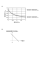
- FIG. 4 is a diagram showing an example of characteristics of the magnetoresistive element 11
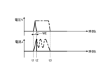
- FIG. 4 is a diagram schematically showing writing of data to the memory cell 10
- FIG. FIG. 10 is a diagram schematically showing data writing according to a comparative example
- FIG. 4 is a diagram schematically showing a stepwise limited current J
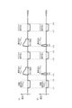
- FIG. 4 is a diagram schematically showing writing of data to the memory cell 10 in the first embodiment
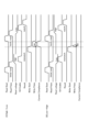
- 4A and 4B are diagrams illustrating an example of control for writing data to the memory cell 10 in the first embodiment
- FIG. 4 is a flow chart showing an example of processing executed in the magnetoresistive memory 100 according to the first embodiment
- FIG. 3 is a diagram showing an example of a schematic configuration of a magnetoresistive memory 100 according to a second embodiment
- FIG. 10 is a diagram showing an example of control of writing data to the memory cell 10 in the second embodiment
- 9 is a flow chart showing an example of processing executed in the magnetoresistive memory 100 of the second embodiment
- FIG. 12 is a diagram schematically showing writing of data to the memory cell 10 in the third embodiment
- FIG. 12 is a diagram showing an example of control of writing data to the memory cell 10 in the third embodiment
- 10 is a flow chart showing an example of processing executed in the magnetoresistive memory 100 according to the third embodiment
- FIG. 11 is a diagram showing an example of a schematic configuration of a magnetoresistive element 11 of a magnetoresistive memory 100 according to a fourth embodiment;
- FIG. 14 is a diagram schematically showing writing of data to the memory cell 10 in the fourth embodiment;
- FIG. 14 is a diagram showing an example of control of writing data to the memory cell 10 in the fourth embodiment;
- FIG. 11 is a flow chart showing an example of processing executed in the magnetoresistive memory 100 according to the fourth embodiment;
- FIG. FIG. 14 is a diagram showing an example of control of writing data to the memory cell 10 in the fifth embodiment;
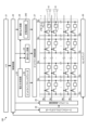
- FIG. 1 is a block diagram showing an example of a schematic configuration of a magnetoresistive memory 100 according to a first embodiment.
- a magnetoresistive memory 100 is a semiconductor memory device using a magnetoresistive element 11 as a memory element.
- a magnetoresistive memory 100 includes a memory cell array 1 .
- the memory cell array 1 includes a plurality of memory cells 10 arranged two-dimensionally. Each memory cell 10 is connected to a bitline BL, a source line SL and a wordline WL. Details of the memory cell 10 will be described later with reference to FIG. 2 and the like.
- the magnetoresistive memory 100 includes various peripheral circuits/elements. As peripheral circuits/elements included in the memory cell array 1, FIG. A wordline address decoder 28, a wordline control circuit 29 and a sense amplifier 30 are illustrated. The bitline control circuit 27 is connected to the bitline BL. A word line control circuit 29 is connected to the word line WL. The sense amplifier 30 is connected to the source line SL. Since the basic configuration of such a memory itself is known, it will be briefly described below.
- commands related to data reading and writing and access target memory cells 10 are transmitted between an external element (for example, a CPU, etc.) of the magnetoresistive memory 100 and the control circuit 22 of the magnetoresistive memory 100. Transfer of addresses, data, etc. is performed.
- an external element for example, a CPU, etc.
- the control circuit 22 controls reading and writing of data in the memory cell 10 according to the command.
- the voltage generation circuit 23 generates a voltage (for example, a pulse voltage) used for reading and writing data in the memory cell 10 . It is assumed that a voltage required for circuit operation is separately applied.
- the write circuit 24 controls the voltage and current (for example, pulse voltage and pulse current) used to write data to the memory cell 10 . Details will be described later.
- the read circuit 25 controls the voltage (for example, pulse voltage) used for reading data from the memory cell 10 , specifically for detecting the resistance value of the magnetoresistive element 11 .
- the bit line address decoder 26 obtains the bit line BL address corresponding to the address received at the I/O 21 described above.
- the bit line control circuit 27 selectively controls the bit line BL corresponding to the address of the bit line address decoder 26 . Writing data to the memory cell 10 by the write circuit 24 and reading data from the memory cell 10 by the read circuit 25 are performed via the bit line control circuit 27 and the like.
- the word line address decoder 28 obtains the word line WL address corresponding to the address received at the I/O 21 described above.
- the word line control circuit 29 selectively controls the word line WL corresponding to the address of the word line address decoder 28.
- the sense amplifier 30 detects data read from the memory cell 10 by the read circuit 25, specifically the resistance value of the magnetoresistive element 11.
- the memory cell 10 will be explained again with reference to FIG. 2 onwards.
- FIG. 2 is a diagram showing an example of a schematic configuration of the memory cell 10.
- FIG. Memory cell 10 includes a magnetoresistive element 11 and a select transistor 12 .
- a magnetoresistive element 11 and a selection transistor 12 are connected in series between a bit line BL and a source line SL.
- the magnetoresistive element 11 is an MTJ element and has a laminated structure.
- an XYZ coordinate system for the magnetoresistive element 11 is illustrated.
- the X-axis direction and the Y-axis direction correspond to the planar direction of the layer.
- the X-axis direction, Y-axis direction, and XY plane direction are also referred to as horizontal directions.
- the Z-axis direction corresponds to a direction (stacking direction) perpendicular to the planar direction of the layers.
- the Z-axis direction is also referred to as the vertical direction.
- a voltage that can be applied to (both ends of) the magnetoresistive element 11 is referred to as voltage V and illustrated.
- a current that can be applied to the magneto-resistive element 11 is referred to as current J and is illustrated.
- Voltage V and current J are controlled by write circuit 24 and read circuit 25 (FIG. 1) and the like.
- the magnetoresistive element 11 includes a fixed layer 111 , a tunnel barrier layer 112 and a recording layer 113 .
- a fixed layer 111, a tunnel barrier layer 112 and a recording layer 113 are laminated in this order in the positive direction of the Z-axis.
- Various known materials may be used for the material of each layer.
- the fixed layer 111 is a magnetic layer whose magnetization direction is fixed, and is also called a reference layer or the like. It is assumed that the magnetization of the fixed layer 111 is fixed in the Z-axis positive direction.
- the tunnel barrier layer 112 is a nonmagnetic layer provided between the fixed layer 111 and the recording layer 113 .
- the recording layer 113 is a magnetic layer whose magnetization direction changes, and is also called a free layer or the like.
- the magnetization of the recording layer 113 changes between the Z-axis positive direction and the Z-axis negative direction.
- the arrangement of the fixed layer 111 and the recording layer 113 may be opposite to the example shown in FIG. In that case, the recording layer 113, the tunnel barrier layer 112 and the fixed layer 111 are laminated in this order in the positive direction of the Z-axis.
- the memory cell 10 is configured such that the recording layer 113 is placed in a magnetic field (horizontal magnetic field) in the plane direction (XY plane direction) of the layer.
- the magnetoresistive element 11 further includes a magnetic field generating layer 114 .
- the magnetic field generating layer 114 generates a horizontal magnetic field.
- the magnetic field generation layer 114 is provided on the side opposite to the tunnel barrier layer 112 with the recording layer 113 interposed therebetween.
- the magnetic field generation layer 114 may be provided on the side opposite to the tunnel barrier layer 112 with the fixed layer 111 interposed therebetween. Also, a technique other than the magnetic field generation layer 114 may be used to generate the horizontal magnetic field. For example, a magnetic field may be generated by forming a magnet layer above (positive direction of the Z-axis) or below (negative direction of the Z-axis) the magnetoresistive element 11 . A magnetic field may be generated by placing permanent magnets around it.
- the selection transistor 12 is a field effect transistor (FET) in this example.
- One of the drain and source of the selection transistor 12 is connected to the magnetoresistive element 11 .
- the other of the drain and source of the selection transistor 12 is connected to the source line SL.
- a gate of the select transistor 12 is connected to the word line WL.
- a voltage signal from the word line WL is applied to the gate of the selection transistor 12, and the selection transistor 12 is turned on (the drain and source are brought into conduction), thereby connecting the magnetoresistive element 11, the bit line BL, and the source line SL. are connected, and a voltage V and a current J are applied to the magnetoresistive element 11 .
- a resistance value of the magnetoresistive element 11 is called a resistance value R.
- FIG. A low resistance value is referred to as a low resistance value R Low .
- a high resistance value is referred to as a high resistance value R High .
- Data corresponding to the low resistance value R Low is also referred to as “Low”.
- Data corresponding to the high resistance value R High is also referred to as "High”. For example, data “Low” corresponds to "0”, and data "High” corresponds to "1".
- the magnetoresistive element 11 is an MTJ element capable of reversing the magnetization of the recording layer 113 by utilizing the VCMA effect. Description will be made with reference to FIG.
- FIG. 3 is a diagram showing an example of the characteristics of the magnetoresistive element 11.
- FIG. FIG. 3A shows the relationship between the magnetization component m Z of the recording layer 113 and the resistance value R of the magnetoresistive element 11 .
- the horizontal axis of the graph indicates the magnetization component m Z of the recording layer 113 .
- the magnetization component mZ is the magnitude of magnetization of the recording layer 113 in the Z-axis direction. When the magnetization component mZ is 1, the magnetization direction of the recording layer 113 is the Z-axis positive direction. When the magnetization component mZ is -1, the magnetization direction of the recording layer 113 is the Z-axis negative direction.
- the vertical axis of the graph indicates the resistance value R of the magnetoresistive element 11 normalized by the high resistance value R HIGH .
- the magnetization component m Z changes between ⁇ 1 and 1 when the magnetization of the recording layer 113 rotates.
- the magnetization direction of the recording layer 113 is the same Z-axis positive direction as the magnetization direction of the fixed layer 111, and the resistance value R of the memory cell array 1 becomes the low resistance value RLow .
- the magnetization component m Z is ⁇ 1
- the magnetization direction of the recording layer 113 is the Z-axis negative direction opposite to the magnetization direction of the fixed layer 111, and the resistance value R of the memory cell array 1 is high.
- the value R goes high .
- the resistance value R of the magnetoresistive element 11 gradually changes between a low resistance value R Low and a high resistance value R High during rotation of the magnetization of the recording layer 113 .
- FIG. 3 shows an example of voltage dependence of the perpendicular magnetic anisotropy constant Ku of the recording layer 113 .
- the horizontal axis of the graph indicates voltage V.
- FIG. The vertical axis of the graph indicates the perpendicular magnetic anisotropy constant Ku of the recording layer 113 .
- the larger the perpendicular magnetic anisotropy constant Ku the easier it is for the recording layer 113 to be magnetized in the perpendicular direction. More specifically, when the perpendicular magnetic anisotropy constant Ku is positive, the recording layer 113 is easily magnetized in the perpendicular direction (Z-axis direction). When the perpendicular magnetic anisotropy constant Ku is negative, the recording layer 113 is easily magnetized in the horizontal direction (XY plane direction).
- the perpendicular magnetic anisotropy constant Ku is positive when the voltage V is 0, that is, when the voltage V is not applied to the magnetoresistive element 11 .
- the recording layer 113 at this time is easily magnetized in the perpendicular direction.
- the value of the perpendicular magnetic anisotropy constant Ku changes. Specifically, as the voltage V increases, the perpendicular magnetic anisotropy constant Ku decreases, and when the voltage V exceeds a certain voltage, the perpendicular magnetic anisotropy constant Ku becomes negative.
- the recording layer 113 at this time is easily magnetized in the horizontal direction.
- the magnetization of the recording layer 113 of the magneto-resistive element 11 undergoes precession about the horizontal magnetic field. It rotates with motion.
- the resistance value R of the magnetoresistive element 11 is switched between a low resistance value R Low and a high resistance value R High , and data is written in the memory cell 10. can be done.
- the voltage is pulsed so that a constant voltage that makes the perpendicular magnetic anisotropy constant Ku 0 is applied only during the reversal period of the magnetization of the recording layer 113 (time required for half rotation).
- the magnetization reversal period of the recording layer 113 depends on the intensity of the magnetic field in the horizontal direction and is short, for example, 0.7 ns. Such pulse control is not easy, and the control becomes even more difficult when element variations are considered.
- write circuit 24 reverses the magnetization of the recording layer 113 so that the resistance value R of the magnetoresistive element 11 switches between the low resistance value R Low and the high resistance value R High .
- write circuit 24 includes current limiting circuit 241 .
- a current limiting circuit 241 limits the current J applied to the magnetoresistive element 11 .
- the current limiting circuit 241 limits the current J to a predetermined level regardless of the resistance value R of the magnetoresistive element 11 .
- “Limiting the current J to a predetermined magnitude” means that when the resistance value R of the magnetoresistive element 11 is too high to apply a current J of a predetermined magnitude, It may be understood to include applying a small current J.
- the write circuit 24 applies to the magneto-resistive element 11 a current J limited to a predetermined magnitude by the current limit circuit 241, thereby reducing the resistance value R of the magneto-resistive element 11 from the high resistance value R High .
- the magnetization of the recording layer 113 is reversed so that the resistance value is switched to R Low .
- a current J is applied to the magnetoresistive element 11
- the magnetization of the recording layer 113 of the magnetoresistive element 11 rotates according to the principle described above.
- the voltage V decreases
- the perpendicular magnetic anisotropy constant Ku of the recording layer 113 increases and the perpendicular magnetic anisotropy returns.
- the resistance value R of the magnetoresistive element 11 becomes the minimum low resistance value R_Low , and the perpendicular magnetic anisotropy constant Ku increases.
- the magnetization of the recording layer 113 stops (automatically) at the timing when the precession stops and is reversed.
- the resistance value R of the magnetoresistive element 11 is switched from the high resistance value R High to the low resistance value R Low , and data “Low” is written in the memory cell 10 .
- FIG. 4 is a diagram schematically showing writing of data to the memory cell 10. As shown in FIG. Voltage V and current J are shown for time t. It is assumed that the resistance value R of the magnetoresistive element 11 is initially the high resistance value R High .
- the write circuit 24 applies the current J limited by the current limiting circuit 241 to the magnetoresistive element 11 .
- the resistance value R of the magnetoresistive element 11 gradually decreases, and the voltage V also decreases gradually.
- the resistance value R of the magnetoresistive element 11 becomes a low resistance value R Low .
- the pulse width of the current J is shown as a pulse width W1.
- the magnetization rotation of the recording layer 113 automatically stops at the timing of reversal, so the pulse width W1 of the current J may be longer than the magnetization reversal period. Accordingly, pulse control becomes easier.
- a comparative example is also used for explanation.
- FIG. 5 is a diagram schematically showing data writing according to a comparative example.
- a constant voltage V having the same pulse width WE as the magnetization reversal period of the recording layer 113 is applied to the magnetoresistive element 11 from time t1 to time t2.
- the resistance value R of the magnetoresistive element 11 becomes a low resistance value R Low .
- the pulse width WE of the voltage V in this comparative example is shorter than the pulse width W1 of the current J in FIG. 4 described above. This makes pulse control difficult. 5, if the pulse width of the voltage V were longer than the pulse width WE, the magnetization of the recording layer 113 would continue to rotate, and the resistance value R and the current J would change. repeat the vibration. The magnetization of the recording layer 113 does not automatically stop at the timing when the magnetization of the recording layer 113 is reversed as shown in FIG. 4 described above. Therefore, in the comparative example, the pulse width WE of the voltage V cannot be lengthened.
- the resistance value R of the magnetoresistive element 11 is changed from the high resistance value R High to It can be switched to a low resistance value R Low .
- the pulse width W1 of the current J may be longer than the magnetization reversal period of the recording layer 113 . Therefore, pulse control for reversing the magnetization of the recording layer 113 is facilitated. For example, since highly accurate pulse control becomes unnecessary, circuit design becomes easier. In addition, it is possible to suppress the deterioration of the success probability of reversing the magnetization of the recording layer 113 (reversal probability) caused by variations in the pulse width and elements.
- the write circuit 24 may apply a current J to the magnetoresistive element 11 that is stepwise limited to different predetermined magnitudes during magnetization reversal of the magnetoresistive element 11 . Description will be made with reference to FIG.
- FIG. 6 is a diagram schematically showing the current J limited step by step.
- the current J is limited to two stages, current J1 and current J2. Initially, current J is limited to current J1. Current J is then limited to current J2, which is greater than current J1. Of course, it is also possible to limit the current J to three or more stages.
- writing data to the memory cell 10 includes initial reading and verify reading. Description will be made with reference to FIG.
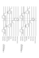
- FIG. 7 is a diagram schematically showing writing of data to the memory cell 10 in the first embodiment.
- FIG. 7A shows changes in the voltage V when the resistance value R of the magnetoresistive element 11 is switched from the high resistance value R High to the low resistance value R Low .
- FIG. 7B shows the change in voltage V when switching the resistance value R of the magnetoresistive element 11 from the low resistance value R Low to the high resistance value R High .
- the read circuit 25 detects the resistance value R of the magnetoresistive element 11 by applying a low voltage that does not reverse the magnetization of the recording layer 113 to the magnetoresistive element 11 .
- a high resistance value R High is detected.
- a low resistance value R Low is detected.
- the write circuit 24 reverses the magnetization of the recording layer 113 so that the resistance value R of the magnetoresistive element 11 switches between a low resistance value RLow and a high resistance value RHigh .
- the write circuit 24 applies a current J (pulse current J) limited by the current limit circuit 241 to the magnetoresistive element 11 whose resistance value R is detected to be the high resistance value R High by the read circuit 25 Width W1) is applied.
- the resistance value R of the magnetoresistive element 11 is switched from the high resistance value R High to the low resistance value R Low , and data "Low" is written.
- FIG. 7A the write circuit 24 applies a current J (pulse current J) limited by the current limit circuit 241 to the magnetoresistive element 11 whose resistance value R is detected to be the high resistance value R High by the read circuit 25 Width W1) is applied.
- the resistance value R of the magnetoresistive element 11 is switched from the high resistance value R High to the low resistance value R Low , and data "L
- the write circuit 24 applies a constant voltage V (pulse width W2) to the magnetoresistive element 11 whose resistance value R is detected to be the low resistance value R Low by the read circuit 25.
- the pulse width W2 of the voltage V may be the same as the magnetization reversal period of the recording layer 113, like the pulse width WE described above with reference to FIG.
- the resistance value R of the magnetoresistive element 11 switches from the low resistance value R Low to the high resistance value R High , and data "High" is written.
- Verify reading is performed from time t14 to time t15.
- the read circuit 25 applies a voltage that does not reverse the magnetization of the recording layer 113 to the magnetoresistive element 11 in order to determine whether the write circuit 24 has successfully switched the resistance value R of the magnetoresistive element 11 .
- 11 resistance value R is detected. It is confirmed whether or not the recording state of the memory cell 10, that is, the resistance value R has been correctly switched.
- Verify reading is performed from time t17 to time t18. Here, it is assumed that the data writing at time t16 was successful. Therefore, data writing is completed.
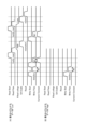
- FIG. 8 is a diagram showing an example of control of writing data to the memory cell 10 in the first embodiment.
- the data in the memory cell 10 is rewritten from "High” to “Low”.
- the data in the memory cell 10 is rewritten from "Low” to "High”.
- the control circuit 22 sends a read start signal (Read Start) to the read circuit 25 .
- the read circuit 25 issues a read pulse (Read Pulse).
- a read pulse is supplied via the bit line control circuit 27 to the bit line BL to which the memory cell 10 to which data is to be written is connected.
- a read voltage from the magnetoresistive element 11 to be accessed is input to the sense amplifier 30 .
- the control circuit 22 enables the sense amplifier 30 (SA Enable). Since the potential changes according to the state of the resistance value R of the magnetoresistive element 11 (the recording state of the memory cell 10), the sense amplifier 30 detects the read voltage (High or Low) when the potential is fixed. This detection corresponds to detection of the resistance value R (high resistance value R High or low resistance value R Low ) of the magnetoresistive element 11, and therefore the data of the memory cell 10 is read.
- the control circuit 22 compares the data of the memory cell 10 read by the sense amplifier 30 with the data to be written.
- the comparison result is a mismatch (Result, mismatch)
- the control circuit 22 sends a write start signal (Write Start) to the write circuit 24 .
- the write circuit 24 issues a write pulse.
- a write pulse is supplied via the bit line control circuit 27 to the bit line BL to which the memory cell 10 to which data is to be written is connected.
- the current J is limited by the current limiting circuit 241 of the write circuit 24 (Current Compliance).
- the write circuit 24 applies a limited current J (pulse width W1) to the magnetoresistive element 11 .
- the resistance value R of the magnetoresistive element 11 is switched from the high resistance value R High to the low resistance value R Low , and data "High” is written.
- the current J is not limited by the current limiting circuit 241 of the write circuit 24 .
- the write circuit 24 applies a constant voltage V (pulse width W2) to the magnetoresistive element 11 .
- V pulse width W2
- the resistance value R of the magnetoresistive element 11 is switched from the low resistance value R Low to the high resistance value R High , and data "Low” is written.
- the control circuit 22 compares the data of the memory cell 10 read by verify read with the data to be written.
- the comparison result is a match (Result, match), and therefore the writing of data ends.
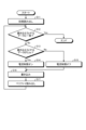
- FIG. 9 is a flowchart showing an example of processing executed in the magnetoresistive memory 100 according to the first embodiment. This flow is controlled, for example, by a state machine within control circuit 22 (FIG. 1). The processing of the flowchart starts when a write command and data to be written are input via the I/O 21 .
- step S11 initial reading is performed.
- the resistance value R of the magnetoresistive element 11 of the memory cell 10 to which data is to be written is detected, and the data of the memory cell 10 is read.
- step S12 it is determined whether or not the read data matches the data to be written. If they match (step S12: Yes), the process of the flowchart ends. Otherwise (step S12: No), the process proceeds to step S13.
- step S13 it is determined whether the data to be written is "Low”. If the data to be written is "Low” (step S13: Yes), the process proceeds to step S14. Otherwise (step S13: No), the process proceeds to step S15.
- step S14 the current limit is turned on.
- the limiting function of the current J by the current limiting circuit 241 of the write circuit 24 is activated. After that, the process proceeds to step S16.
- step 15 the current limit is turned off.
- the limiting function of the current J by the current limiting circuit 241 of the write circuit 24 is not enabled (disabled). After that, the process proceeds to step S16.
- step S16 data is written.
- the current J pulse width W1
- the current limiting circuit 241 is applied to the magnetoresistive element 11.
- FIG. The resistance value R of the magnetoresistive element 11 is switched from the high resistance value R High to the low resistance value R Low , and data "Low” is written.
- a constant voltage V pulse width W2 is applied to the magnetoresistive element 11 .
- the resistance value R of the magnetoresistive element 11 is switched from the low resistance value R Low to the high resistance value R High , and data "High” is written.
- step S17 verify reading is performed. After that, the process is returned to step S12. If the read data matches the data to be written (step S12: Yes), the processing of the flowchart ends. Otherwise (step S12: No), the process proceeds to step S13.
- An upper limit may be set for the number of verify readings and rewritings, that is, the number of loops of steps S12 to S17 after step S17.
- FIG. 10 is a diagram showing an example of a schematic configuration of a magnetoresistive memory 100 according to a second embodiment.
- the magnetoresistive memory 100 of the second embodiment differs from the first embodiment (FIG. 1) in that the write circuit 24 includes a constant current circuit 242 .
- the constant current circuit 242 keeps the current J applied to the magnetoresistive element 11 constant (constant current).
- the limited current J in the first embodiment described above is a constant current in the second embodiment.
- FIG. 11 is a diagram showing an example of control of writing data to the memory cell 10 in the second embodiment.
- the difference is that instead of the current limit (Current Compliance) by the current limit circuit 241, the constant current circuit 242 is used to make the current constant (Current Constant).
- Other controls are the same as those in the first embodiment, so the description will not be repeated.
- FIG. 12 is a flowchart showing an example of processing executed in the magnetoresistive memory 100 of the second embodiment.
- the processing of steps S21 to S23 and step S27 is the same as the processing of steps S11 to S13 and step S17 of the first embodiment (FIG. 9), so the description will not be repeated.
- step S24 the constant current is turned on.
- the constant current function of the current J by the constant current circuit 242 of the write circuit 24 is enabled. After that, the process proceeds to step S26.
- step S25 the constant current is turned off.
- the constant current function of the current J by the constant current circuit 242 of the write circuit 24 is not enabled (disabled). After that, the process proceeds to step S26.
- step S26 data is written.
- the current J pulse width W1 made constant by the constant current circuit 242 is applied to the magnetoresistive element 11.
- FIG. The resistance value R of the magnetoresistive element 11 is switched from the high resistance value R High to the low resistance value R Low , and data "Low” is written.
- a constant voltage V pulse width W2 is applied to the magnetoresistive element 11 .
- the resistance value R of the magnetoresistive element 11 is switched from the low resistance value R Low to the high resistance value R High , and data "High” is written.
- writing data to the memory cell 10 includes initialization instead of initial reading. Initialization eliminates the need for initial reading.
- the basic configuration of the magnetoresistive memory 100 is the same as that of the first embodiment (FIG. 1) or the second embodiment (FIG. 10). Unless otherwise specified, the third embodiment and subsequent embodiments will be described assuming that they have the configuration shown in FIG.
- the write circuit 24 applies a constant current J to the magnetoresistive element 11 by the constant current circuit 242 to initialize the resistance value R of the magnetoresistive element 11 to a low resistance value R Low .
- the resistance value R of the magnetoresistive element 11, which was the low resistance value R Low before initialization remains at the low resistance value R Low because the voltage V is low and precession does not occur even if the current J is applied. .
- FIG. 13 is a diagram schematically showing writing of data to the memory cell 10 in the third embodiment.
- the data before initialization is “High”, and the data to be written is also “High”.
- the data before initialization is "High” and the data to be written is “Low”.
- the data before initialization is "Low” and the data to be written is "High”.
- the data before initialization is "Low" and the data to be written is also "Low”.
- Initialization is performed from time t31 to time t32.
- the write circuit 24 applies a constant current J to the magnetoresistive element 11 by the constant current circuit 242 to initialize the resistance value R of the magnetoresistive element 11 to a low resistance value R Low .
- the resistance value R of the magnetoresistive element 11 switches from the high resistance value R High to the low resistance value R Low .
- the resistance value R of the magnetoresistive element 11 remains at the high resistance value R High (no change).
- Data is written as necessary from time t33 to time t34.
- data "High” is written.
- a constant voltage V (pulse width W2) is applied to the magnetoresistive element 11, and the resistance value R of the magnetoresistive element 11 switches from the low resistance value R Low to the high resistance value R High .
- Data is not written in (B) and (D) of FIG.
- verify reading is performed as necessary.
- verify reading is performed in accordance with the previous data writing from time t33 to time t34. Here, it is assumed that the data writing has succeeded. Therefore, data writing is completed.
- verify reading is omitted and data writing is completed. However, verify reading may be performed in (B) and (D) of FIG. 13 as well.
- FIG. 14 is a diagram showing an example of control of writing data to the memory cell 10 in the third embodiment.
- data "Low” is written.
- data "High” is written.
- the write circuit 24 issues a write pulse.
- a write pulse is supplied via the bit line control circuit 27 to the bit line BL to which the memory cell 10 to which data is to be written is connected.
- the constant current circuit 242 of the write circuit 24 makes the current J constant (Current Constant).
- the write circuit 24 applies a current J (pulse width W1) made constant by the constant current circuit 242 to the magnetoresistive element 11 .
- the resistance value R of the magnetoresistive element 11 is initialized to the low resistance value R Low .
- FIG. 14B data "High” is written.
- the write circuit 24 issues a write pulse.
- the write circuit 24 applies a constant voltage V (pulse width W2) to the magnetoresistive element 11 .
- V pulse width W2
- the resistance value R of the magnetoresistive element 11 switches from the low resistance value R Low to the high resistance value R High .
- a verify read is performed.
- the comparison result is a mismatch (Result, mismatch)
- the comparison result is a match (Result, match)
- data writing is completed.
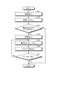
- FIG. 15 is a flowchart showing an example of processing executed in the magnetoresistive memory 100 according to the third embodiment.
- the constant current is turned on.
- the constant current function of the current J by the constant current circuit 242 is activated.
- step 32 initialization takes place.
- a constant current J pulse width W1 is applied to all the magnetoresistive elements 11 (all bits) of the designated address.
- the resistance value R of the magnetoresistive element 11 is initialized to a low resistance value R Low .
- step S33 it is determined whether the data to be written is "High". If the data to be written is "High” (step S33: Yes), the process proceeds to step S34. Otherwise (step S33: No), the process of the flowchart ends.
- the constant current is turned off.
- the constant current function of the current J by the current limiting circuit 241 is not enabled (disabled).
- step S35 data is written.
- a constant voltage V pulse width W2
- the resistance value R of the magnetoresistive element 11 switches from the low resistance value R Low to the high resistance value R High .
- step S36 verify reading is performed.
- step S37 it is determined whether or not the read data matches the data to be written. If they match (step S37: Yes), the process of the flowchart ends. Otherwise (step S27: No), the process returns to step S35 and data is written again.
- the resistance value R of the magnetoresistive element 11 is initialized to a high resistance value R High using the technique of Non-Patent Document 1.
- FIG. According to the technique of Non-Patent Document 1, pulse control of the voltage V when switching the resistance value R of the magnetoresistive element 11 from the low resistance value R Low to the high resistance value R High is facilitated. The effect of facilitating pulse control for reversing the magnetization of the recording layer 113 is further enhanced.
- the perpendicular magnetic field causes the change in magnetic field energy with respect to the magnetization component m Z ( ⁇ 1 to 1) of the recording layer 113 to have an asymmetry.
- the magnetic field energy is minimized in the range where the magnetization component m Z becomes negative ( ⁇ 1 ⁇ magnetization component m Z ⁇ 0), that is, when the magnetization of the recording layer 113 approaches the negative direction of the Z axis. can be suppressed and reversed in the Z-axis negative direction.
- the resistance value R of the magnetoresistive element 11 can be set to the high resistance value R High without controlling the pulse width of the voltage V with high accuracy.
- FIG. 16 is a diagram showing an example of a schematic configuration of the magnetoresistive element 11 of the magnetoresistive memory 100 according to the fourth embodiment.
- the memory cell 10 is configured such that the recording layer 113 is also placed in a vertical (Z-axis) magnetic field (perpendicular magnetic field).
- the magnetoresistive element 11 further includes a magnetic field generating layer 115 .
- the magnetic field generating layer 115 generates a perpendicular magnetic field.
- the magnetic field generating layer 115 is provided on the side opposite to the tunnel barrier layer 112 with the fixed layer 111 interposed therebetween.
- the magnetic field generation layer 115 may be provided on the side opposite to the tunnel barrier layer 112 with the recording layer 113 interposed therebetween. Techniques other than the magnetic field generating layer 115 may be used to generate the perpendicular magnetic field. For example, a magnetic field may be generated by forming a magnet layer above (positive direction of the Z-axis) or below (negative direction of the Z-axis) the magnetoresistive element 11 . A magnetic field may be generated by placing permanent magnets around it.
- FIG. 17 is a diagram schematically showing writing of data to the memory cell 10 in the fourth embodiment.
- the data before initialization is “High”, and the data to be written is also “High”.
- the data before initialization is “High”, and the data to be written is also “Low”.
- the data before initialization is "Low” and the data to be written is "High”.
- the data before initialization is "Low”, and the data to be written is also "Low”.
- Initialization is performed from time t41 to time t42.
- the write circuit 24 applies a constant voltage V (pulse width W3) to the magnetoresistive element 11 to initialize the resistance value R of the magnetoresistive element 11 to a high resistance value RHigh .
- the pulse width W3 of the voltage V here may be longer than the pulse width W2 (FIGS. 7, 13, etc.).
- the resistance value R of the magnetoresistive element 11 remains at the high resistance value R High (no change).
- the resistance value R of the magnetoresistive element 11 is switched from the low resistance value R Low to the high resistance value R High .
- Data is written as necessary from time t43 to time t44. Data is not written in (A) and (C) of FIG. In (B) and (D) of FIG. 17, data is written.
- a current J pulse width W1 made constant by the constant current circuit 242 is applied to the magnetoresistive element 11, and the resistance value R of the magnetoresistive element 11 is switched from the high resistance value R High to the low resistance value R Low .
- verify reading is performed as necessary.
- verify reading is omitted and data writing is completed. However, verify reading may be performed.
- verify reading is performed according to the previous data writing from time t43 to time t44. Here, it is assumed that the data writing has succeeded. Therefore, data writing is completed.
- FIG. 18 is a diagram showing an example of control of writing data to the memory cell 10 in the fourth embodiment.
- FIG. 18A shows control when writing data "Low”.
- FIG. 18B shows control when writing data "High”.
- the write circuit 24 issues a write pulse.
- a write pulse is supplied via the bit line control circuit 27 to the bit line BL to which the memory cell 10 to which data is to be written is connected.
- the write circuit 24 applies a constant voltage V (pulse width W3) to the magnetoresistive element 11 .
- the resistance value R of the magnetoresistive element 11 is initialized to the high resistance value R High .
- FIG. 18A data "Low” is written.
- the write circuit 24 issues a write pulse.
- the write circuit 24 applies a current J (pulse width W1) made constant by the constant current circuit 242 to the magnetoresistive element 11 .
- the resistance value R of the magnetoresistive element 11 switches from the high resistance value R High to the low resistance value R Low .
- a verify read is performed.
- the comparison result is a mismatch (Result, mismatch), so the data is written again.
- the comparison result is a match (Result, match)
- data writing is completed.
- FIG. 19 is a flowchart showing an example of processing executed in the magnetoresistive memory 100 according to the fourth embodiment.
- step S41 Initialization is performed in step S41.
- a constant voltage V pulse width W3 is applied to all the magnetoresistive elements 11 (all bits) of the designated address.
- the resistance value R of the magnetoresistive element 11 is initialized to a high resistance value R High .
- step S42 it is determined whether the data to be written is "Low". If the data to be written is "Low" (step S42: Yes), the process proceeds to step S43. Otherwise (step S4: No), the process of the flowchart ends.
- the constant current is turned on.
- the constant current function of the current J by the constant current circuit 242 is activated.
- step S44 data is written.
- a constant current J (pulse width W1) controlled by a constant current circuit 242 is applied to the magnetoresistive element 11 .
- the resistance value R of the magnetoresistive element 11 switches from the high resistance value R High to the low resistance value R Low .
- step S45 verify reading is performed.
- step S46 it is determined whether or not the read data matches the data to be written. If they match (step S46: Yes), the process of the flowchart ends. Otherwise (step S46: No), the process returns to step S44 and data is written again.
- initial reading is performed, and the resistance value R of the magnetoresistive element 11 is switched between a low resistance value R Low and a high resistance value R High as necessary. For example, when writing data "High" in step S16 of FIG. 9 or step S26 of FIG. The value R switches from a low resistance value R Low to a high resistance value R High .
- FIG. 20 is a diagram showing an example of control of writing data to the memory cell 10 in the fifth embodiment.
- FIG. 20A shows control when writing data "Low”.
- FIG. 20B shows control when writing data "High”.
- (A) of FIG. 20 is the same as (A) of FIG. 11 described above.
- the voltage V with the pulse width W3 is applied as compared with FIG. 11B described above. They are different in that they are applied. Application of a voltage V with a short pulse width W2 as shown in FIG. 11B is unnecessary.
- the magnetoresistive memory 100 includes a fixed layer 111 whose magnetization direction is fixed and a recording layer 113 whose magnetization direction changes. It includes a magnetoresistive element 11 and a write circuit 24 that reverses the magnetization of the recording layer 113 so that the resistance value R of the magnetoresistive element 11 switches between a low resistance value R Low and a high resistance value R High .
- the magnetization of the recording layer 113 rotates due to precession around the magnetic field (horizontal magnetic field) in the plane direction (XY plane direction) of the layer when a voltage V is applied to the magnetoresistive element 11 .
- the resistance value R of the magnetoresistive element 11 gradually changes between a low resistance value R Low and a high resistance value R High during rotation of the magnetization of the recording layer 113, and the write circuit 24 reaches a predetermined magnitude.
- the magnetization of the recording layer 113 is reversed so that the resistance value R of the magnetoresistive element 11 is switched from the high resistance value R High to the low resistance value R Low .
- the write circuit 24 may apply a limited current J having a pulse width W ⁇ b>1 longer than the magnetization reversal period of the recording layer 113 to the magnetoresistive element 11 .
- the resistance value R of the magnetoresistive element 11 changes from a high resistance value R High to a low resistance value. It switches to the value R Low . Since the pulse width W1 of the current J may be longer than the magnetization reversal period of the recording layer 113, pulse control for reversing the magnetization of the recording layer 113 is facilitated.
- the limited current J may be a constant current.
- the resistance value R of the magnetoresistive element 11 can also be switched from the high resistance value RHigh to the low resistance value RLow .
- the write circuit 24 controls the current J (for example, the current J1 and the current J2) may be applied to the magnetoresistive element 11 .
- the resistance value R of the magnetoresistive element 11 can also be switched from the high resistance value RHigh to the low resistance value RLow .
- the write circuit 24 applies a constant voltage V to the magnetoresistive element 11 to change the resistance value R of the magnetoresistive element 11 from a low resistance value R Low to a high resistance value.
- the magnetization of the recording layer 113 may be reversed so as to switch to R High .
- the write circuit 24 may apply a constant voltage V having the same pulse width W2 as the magnetization reversal period of the recording layer 113 to the magnetoresistive element 11 .
- the resistance value R of the magnetoresistive element 11 can be set to the high resistance value R High .
- the magnetoresistive memory 100 applies a voltage that does not reverse the magnetization of the recording layer 113 to the magnetoresistive element 11 so that the magnetoresistive element 11
- a readout circuit 25 for detecting the resistance value R may be provided.
- the write circuit 24 applies the limited current J to the magnetoresistive element 11 whose resistance value R is detected as the high resistance value R High by the read circuit 25, thereby increasing the resistance of the magnetoresistive element 11.
- the magnetization of the recording layer 113 may be reversed such that the value R switches from a high resistance value R High to a low resistance value R Low . In this way, data can be written to the memory cell 10 by switching the resistance value R of the magnetoresistive element 11 as necessary after performing the initial reading.
- the write circuit 24 reduces the resistance value R of the magnetoresistive element 11 to the low resistance value R Low by applying a limited current J to the magnetoresistive element 11.
- the recording layer 113 is changed so that the resistance value R of the magnetoresistive element 11 is switched from the low resistance value R Low to the high resistance value R High . may be reversed.
- Initialization eliminates the need for initial reading.
- the write circuit 24 controls the recording layer to determine whether the write circuit 24 has successfully switched the resistance value R of the magnetoresistive element 11.
- the resistance value R of the magnetoresistive element 11 may be detected by applying to the magnetoresistive element 11 a low voltage at which the magnetization of 113 is not reversed. Verify reading can also be performed in this manner.
- the magnetization of the recording layer 113 is a magnetic field in the plane direction of the layer in a magnetic field (perpendicular magnetic field) perpendicular to the plane direction of the layer (in the Z-axis direction).
- the write circuit 24 may apply a constant voltage V having a pulse width W3 longer than the magnetization reversal period of the recording layer 113 to the magnetoresistive element 11. . This facilitates pulse control of the voltage V when switching the resistance value R of the magnetoresistive element 11 from the low resistance value R Low to the high resistance value R High . The effect of facilitating pulse control for reversing the magnetization of the recording layer 113 is further enhanced.
- the write circuit 24 applies a constant voltage V to the magnetoresistive element 11 to initialize the resistance value R of the magnetoresistive element 11 to the high resistance value R High .
- V a constant voltage
- J a limited current J
- the recording layer 113 is changed so that the resistance value R of the magnetoresistive element 11 is switched from a high resistance value RHigh to a low resistance value RLow . may be reversed.
- Initialization eliminates the need for initial reading.
- a magnetoresistive element including a fixed layer with a fixed magnetization direction and a recording layer with a variable magnetization direction; a write circuit that reverses the magnetization of the recording layer so that the resistance value of the magnetoresistive element switches between a low resistance value and a high resistance value; with The magnetization of the recording layer is rotated by precession around the magnetic field in the plane direction of the layer when a voltage is applied to the magnetoresistive element, the resistance value of the magnetoresistive element gradually changes between a low resistance value and a high resistance value during rotation of the magnetization of the recording layer; The write circuit applies a current limited to a predetermined magnitude to the magnetoresistive element so that the resistance value of the magnetoresistive element switches from a high resistance value to a low resistance value.
- Magnetoresistive memory (2) The write circuit applies the limited current having a pulse width longer than the magnetization reversal period of the recording layer to the magnetoresistive element.
- the write circuit applies currents to the magnetoresistive element that are stepwise limited to different predetermined magnitudes during reversal of the magnetization of the recording layer; A magnetoresistive memory according to any one of (1) to (3).
- the write circuit reverses the magnetization of the recording layer by applying a constant voltage to the magnetoresistive element so that the resistance value of the magnetoresistive element switches from a low resistance value to a high resistance value.
- a magnetoresistive memory according to any one of (1) to (4).
- the write circuit applies the constant voltage having the same pulse width as the magnetization reversal period of the recording layer to the magnetoresistive element, (5) The magnetoresistive memory as described in (5).
- a reading circuit that detects the resistance value of the magnetoresistive element by applying a voltage that does not reverse the magnetization of the recording layer to the magnetoresistive element, A magnetoresistive memory according to any one of (1) to (6).
- the write circuit applies the limited current to the magnetoresistive element whose resistance value is detected to be a high resistance value by the readout circuit, thereby increasing the resistance value of the magnetoresistive element from the high resistance value. reversing the magnetization of the recording layer such that it switches to a low resistance value;
- the magnetoresistive memory according to (7).
- the write circuit initializes the resistance value of the magnetoresistive element to a low resistance value by applying the limited current to the magnetoresistive element, and applies a constant voltage to the magnetoresistive element after initialization.
- the magnetization of the recording layer is reversed so that the resistance value of the magnetoresistive element switches from a low resistance value to a high resistance value, A magnetoresistive memory according to any one of (1) to (6).
- a low voltage that does not reverse the magnetization of the recording layer is applied to the magnetoresistive element to change the resistance value of the magnetoresistive element. comprising a readout circuit for detecting A magnetoresistive memory according to any one of (1) to (9).
- the magnetization of the recording layer rotates in a magnetic field perpendicular to the plane direction of the layer due to the precession around the magnetic field in the plane direction of the layer;
- the write circuit applies the constant voltage having a pulse width longer than the magnetization reversal period of the recording layer to the magnetoresistive element, (5) The magnetoresistive memory as described in (5).
- the write circuit initializes the resistance value of the magnetoresistive element to a high resistance value by applying the constant voltage to the magnetoresistive element, and applies the limited current to the magnetoresistive element after initialization. By doing so, the magnetization of the recording layer is reversed so that the resistance value of the magnetoresistive element switches from a high resistance value to a low resistance value, (11) The magnetoresistive memory according to (11).
- Magnetoresistive Effect Memory 1 Memory Cell Array 10 Memory Cell 11 Magnetoresistive Element 111 Fixed Layer 112 Tunnel Barrier Layer 113 Recording Layer 114 Magnetic Field Generation Layer 115 Magnetic Field Generation Layer 12 Selection Transistor 21 I/O 22 control circuit 23 voltage generation circuit 24 write circuit 241 current limiting circuit 242 constant current circuit 25 read circuit 26 bit line address decoder 27 bit line control circuit 28 word line address decoder 29 word line control circuit 30 sense amplifier J current J1 current J2 current Ku Perpendicular magnetic anisotropy constant V Voltage BL Bit line SL Source line WL Word line W1 Pulse width W2 Pulse width W3 Pulse width WE Pulse width
Landscapes
- Engineering & Computer Science (AREA)
- Computer Hardware Design (AREA)
- Hall/Mr Elements (AREA)
- Mram Or Spin Memory Techniques (AREA)
- Semiconductor Memories (AREA)
Abstract
Description
1.第1実施形態
2.第2実施形態
3.第3実施形態
4.第4実施形態
5.第5実施形態
6.効果の例
図1は、第1実施形態に係る磁気抵抗効果メモリ100の概略構成の例を示すブロック図である。磁気抵抗効果メモリ100は、磁気抵抗素子11を記憶素子として用いる半導体記憶装置である。磁気抵抗効果メモリ100は、メモリセルアレイ1を含む。
図10は、第2実施形態に係る磁気抵抗効果メモリ100の概略構成の例を示す図である。第2実施形態の磁気抵抗効果メモリ100は、第1実施形態形態(図1)と比較して、書き込み回路24が定電流回路242を含む点において相違する。定電流回路242は、磁気抵抗素子11に印加される電流Jを一定にする(定電流化する)。換言すると、先に説明した実施形態1での制限された電流Jが、第2実施形態では定電流である。
第3実施形態では、メモリセル10へのデータの書き込みは、初期読み出しを含まない代わりに、初期化を含む。初期化を行うことで、初期読み出しが不要になる。磁気抵抗効果メモリ100の基本的な構成は、第1実施形態(図1)又は第2実施形態(図10)と同様である。とくに説明がある場合を除き、第3実施形態以降は、図10の構成であるものとして説明する。
第4実施形態では、非特許文献1の技術を用いて、磁気抵抗素子11の抵抗値Rが、高抵抗値RHighに初期化される。非特許文献1の技術によれば、磁気抵抗素子11の抵抗値Rを低抵抗値RLowから高抵抗値RHighに切り替える際の電圧Vのパルス制御が容易になる。記録層113の磁化を反転させるためのパルス制御を容易にする効果がさらに高められる。
第5実施形態では、初期読み出しを行い、必要に応じて、磁気抵抗素子11の抵抗値Rを低抵抗値RLow及び高抵抗値RHighの間で切り替える。例えば先に説明した図9のステップS16や図12のステップS26においてデータ“High”を書き込むときに、一定の電圧V(パルス幅W3)が磁気抵抗素子11に印加され、磁気抵抗素子11の抵抗値Rが低抵抗値RLowから高抵抗値RHighに切り替わる。
以上で説明した技術は、例えば次のように特定される。開示される技術の1つは、磁気抵抗効果メモリ100である。図1~図4及び図6~図9等を参照して説明したように、磁気抵抗効果メモリ100は、磁化の向きが固定された固定層111及び磁化の向きが変化する記録層113を含む磁気抵抗素子11と、磁気抵抗素子11の抵抗値Rが低抵抗値RLow及び高抵抗値RHighの間で切り替わるように、記録層113の磁化を反転させる書き込み回路24と、を備える。記録層113の磁化は、磁気抵抗素子11に電圧Vが印加されているときに、層の面方向(XY平面方向)の磁場(水平磁場)を軸とする歳差運動により回転する。磁気抵抗素子11の抵抗値Rは、記録層113の磁化の回転中に、低抵抗値RLow及び高抵抗値RHighの間で徐々に変化し、書き込み回路24は、所定の大きさになるように制限された電流Jを磁気抵抗素子11に印加することにより、磁気抵抗素子11の抵抗値Rが高抵抗値RHighから低抵抗値RLowに切り替わるように、記録層113の磁化を反転させる。書き込み回路24は、記録層113の磁化の反転期間よりも長いパルス幅W1を有する制限された電流Jを磁気抵抗素子11に印加してよい。
(1)
磁化の向きが固定された固定層及び磁化の向きが変化する記録層を含む磁気抵抗素子と、
前記磁気抵抗素子の抵抗値が低抵抗値及び高抵抗値の間で切り替わるように、前記記録層の磁化を反転させる書き込み回路と、
を備え、
前記記録層の磁化は、前記磁気抵抗素子に電圧が印加されているときに、層の面方向の磁場を軸とする歳差運動により回転し、
前記磁気抵抗素子の抵抗値は、前記記録層の磁化の回転中に、低抵抗値及び高抵抗値の間で徐々に変化し、
前記書き込み回路は、所定の大きさになるように制限された電流を前記磁気抵抗素子に印加することにより、前記磁気抵抗素子の抵抗値が高抵抗値から低抵抗値に切り替わるように、前記記録層の磁化を反転させる、
磁気抵抗効果メモリ。
(2)
前記書き込み回路は、前記記録層の磁化の反転期間よりも長いパルス幅を有する前記制限された電流を前記磁気抵抗素子に印加する、
(1)に記載の磁気抵抗効果メモリ。
(3)
前記制限された電流は、定電流である、
(1)又は(2)に記載の磁気抵抗効果メモリ。
(4)
前記書き込み回路は、前記記録層の磁化の反転中に、異なる所定の大きさになるように段階的に制限された電流を前記磁気抵抗素子に印加する、
(1)~(3)のいずれかに記載の磁気抵抗効果メモリ。
(5)
前記書き込み回路は、一定の電圧を前記磁気抵抗素子に印加することにより、前記磁気抵抗素子の抵抗値が低抵抗値から高抵抗値に切り替わるように、前記記録層の磁化を反転させる、
(1)~(4)のいずれかに記載の磁気抵抗効果メモリ。
(6)
前記書き込み回路は、前記記録層の磁化の反転期間と同じパルス幅を有する前記一定の電圧を前記磁気抵抗素子に印加する、
(5)に記載の磁気抵抗効果メモリ。
(7)
前記記録層の磁化が反転しない電圧を前記磁気抵抗素子に印加することにより、前記磁気抵抗素子の抵抗値を検出する読み出し回路を備える、
(1)~(6)のいずれかに記載の磁気抵抗効果メモリ。
(8)
前記書き込み回路は、前記読み出し回路によって抵抗値が高抵抗値であると検出された前記磁気抵抗素子に、前記制限された電流を印加することにより、前記磁気抵抗素子の抵抗値が高抵抗値から低抵抗値に切り替わるように、前記記録層の磁化を反転させる、
(7)に記載の磁気抵抗効果メモリ。
(9)
前記書き込み回路は、前記磁気抵抗素子に前記制限された電流を印加することにより前記磁気抵抗素子の抵抗値を低抵抗値に初期化し、初期化後の前記磁気抵抗素子に一定の電圧を印加することにより、前記磁気抵抗素子の抵抗値が低抵抗値から高抵抗値に切り替わるように、前記記録層の磁化を反転させる、
(1)~(6)のいずれかに記載の磁気抵抗効果メモリ。
(10)
前記書き込み回路による前記磁気抵抗素子の抵抗値の切り替えの成否を判別するために、前記記録層の磁化が反転しない低電圧を前記磁気抵抗素子に印加することにより、前記磁気抵抗素子の抵抗値を検出する読み出し回路を備える、
(1)~(9)のいずれかに記載の磁気抵抗効果メモリ。
(11)
前記記録層の磁化は、層の面方向に垂直な磁場の中で、前記層の面方向の磁場を軸とする前記歳差運動により回転し、
前記書き込み回路は、前記記録層の磁化の反転期間よりも長いパルス幅を有する前記一定の電圧を前記磁気抵抗素子に印加する、
(5)に記載の磁気抵抗効果メモリ。
(12)
前記書き込み回路は、前記磁気抵抗素子に前記一定の電圧を印加することにより前記磁気抵抗素子の抵抗値を高抵抗値に初期化し、初期化後の前記磁気抵抗素子に前記制限された電流を印加することにより、前記磁気抵抗素子の抵抗値が高抵抗値から低抵抗値に切り替わるように、前記記録層の磁化を反転させる、
(11)に記載の磁気抵抗効果メモリ。
1 メモリセルアレイ
10 メモリセル
11 磁気抵抗素子
111 固定層
112 トンネル障壁層
113 記録層
114 磁場生成層
115 磁場生成層
12 選択トランジスタ
21 I/O
22 制御回路
23 電圧生成回路
24 書き込み回路
241 電流制限回路
242 定電流回路
25 読み出し回路
26 ビットラインアドレスデコーダ
27 ビットライン制御回路
28 ワードラインアドレスデコーダ
29 ワードライン制御回路
30 センスアンプ
J 電流
J1 電流
J2 電流
Ku 垂直磁気異方性定数
V 電圧
BL ビットライン
SL ソースライン
WL ワードライン
W1 パルス幅
W2 パルス幅
W3 パルス幅
WE パルス幅
Claims (10)
- 磁化の向きが固定された固定層及び磁化の向きが変化する記録層を含む磁気抵抗素子と、
前記磁気抵抗素子の抵抗値が低抵抗値及び高抵抗値の間で切り替わるように、前記記録層の磁化を反転させる書き込み回路と、
を備え、
前記記録層の磁化は、前記磁気抵抗素子に電圧が印加されているときに、層の面方向の磁場を軸とする歳差運動により回転し、
前記磁気抵抗素子の抵抗値は、前記記録層の磁化の回転中に、低抵抗値及び高抵抗値の間で徐々に変化し、
前記書き込み回路は、所定の大きさになるように制限された電流を前記磁気抵抗素子に印加することにより、前記磁気抵抗素子の抵抗値が高抵抗値から低抵抗値に切り替わるように、前記記録層の磁化を反転させる、
磁気抵抗効果メモリ。 - 前記書き込み回路は、前記記録層の磁化の反転期間よりも長いパルス幅を有する前記制限された電流を前記磁気抵抗素子に印加する、
請求項1に記載の磁気抵抗効果メモリ。 - 前記制限された電流は、定電流である、
請求項1に記載の磁気抵抗効果メモリ。 - 前記書き込み回路は、前記記録層の磁化の反転中に、異なる所定の大きさになるように段階的に制限された電流を前記磁気抵抗素子に印加する、
請求項1に記載の磁気抵抗効果メモリ。 - 前記書き込み回路は、一定の電圧を前記磁気抵抗素子に印加することにより、前記磁気抵抗素子の抵抗値が低抵抗値から高抵抗値に切り替わるように、前記記録層の磁化を反転させる、
請求項1に記載の磁気抵抗効果メモリ。 - 前記書き込み回路は、前記記録層の磁化の反転期間と同じパルス幅を有する前記一定の電圧を前記磁気抵抗素子に印加する、
請求項5に記載の磁気抵抗効果メモリ。 - 前記記録層の磁化が反転しない電圧を前記磁気抵抗素子に印加することにより、前記磁気抵抗素子の抵抗値を検出する読み出し回路を備える、
請求項1に記載の磁気抵抗効果メモリ。 - 前記書き込み回路は、前記読み出し回路によって抵抗値が高抵抗値であると検出された前記磁気抵抗素子に、前記制限された電流を印加することにより、前記磁気抵抗素子の抵抗値が高抵抗値から低抵抗値に切り替わるように、前記記録層の磁化を反転させる、
請求項7に記載の磁気抵抗効果メモリ。 - 前記書き込み回路は、前記磁気抵抗素子に前記制限された電流を印加することにより前記磁気抵抗素子の抵抗値を低抵抗値に初期化し、初期化後の前記磁気抵抗素子に一定の電圧を印加することにより、前記磁気抵抗素子の抵抗値が低抵抗値から高抵抗値に切り替わるように、前記記録層の磁化を反転させる、
請求項1に記載の磁気抵抗効果メモリ。 - 前記書き込み回路による前記磁気抵抗素子の抵抗値の切り替えの成否を判別するために、前記記録層の磁化が反転しない低電圧を前記磁気抵抗素子に印加することにより、前記磁気抵抗素子の抵抗値を検出する読み出し回路を備える、
請求項1に記載の磁気抵抗効果メモリ。
Priority Applications (3)
| Application Number | Priority Date | Filing Date | Title |
|---|---|---|---|
| CN202380020236.9A CN118661224A (zh) | 2022-02-10 | 2023-01-19 | 磁阻效应存储器 |
| US18/835,824 US20250140297A1 (en) | 2022-02-10 | 2023-01-19 | Magnetoresistive effect memory |
| KR1020247028721A KR20240144260A (ko) | 2022-02-10 | 2023-01-19 | 자기 저항 효과 메모리 |
Applications Claiming Priority (2)
| Application Number | Priority Date | Filing Date | Title |
|---|---|---|---|
| JP2022019641A JP2023117115A (ja) | 2022-02-10 | 2022-02-10 | 磁気抵抗効果メモリ |
| JP2022-019641 | 2022-02-10 |
Publications (1)
| Publication Number | Publication Date |
|---|---|
| WO2023153162A1 true WO2023153162A1 (ja) | 2023-08-17 |
Family
ID=87564310
Family Applications (1)
| Application Number | Title | Priority Date | Filing Date |
|---|---|---|---|
| PCT/JP2023/001497 Ceased WO2023153162A1 (ja) | 2022-02-10 | 2023-01-19 | 磁気抵抗効果メモリ |
Country Status (6)
| Country | Link |
|---|---|
| US (1) | US20250140297A1 (ja) |
| JP (1) | JP2023117115A (ja) |
| KR (1) | KR20240144260A (ja) |
| CN (1) | CN118661224A (ja) |
| TW (1) | TW202347327A (ja) |
| WO (1) | WO2023153162A1 (ja) |
Cited By (1)
| Publication number | Priority date | Publication date | Assignee | Title |
|---|---|---|---|---|
| WO2025239167A1 (ja) * | 2024-05-16 | 2025-11-20 | ソニーセミコンダクタソリューションズ株式会社 | 記憶装置、電子機器および記憶装置の制御方法 |
Citations (1)
| Publication number | Priority date | Publication date | Assignee | Title |
|---|---|---|---|---|
| JP2019021356A (ja) * | 2017-07-12 | 2019-02-07 | 株式会社東芝 | 磁気メモリ |
Family Cites Families (4)
| Publication number | Priority date | Publication date | Assignee | Title |
|---|---|---|---|---|
| JP2008098515A (ja) * | 2006-10-13 | 2008-04-24 | Toshiba Corp | 磁気ランダムアクセスメモリ及びその製造方法 |
| US8134864B2 (en) * | 2008-08-14 | 2012-03-13 | Regents Of The University Of Minnesota | Exchange-assisted spin transfer torque switching |
| JP2010225783A (ja) * | 2009-03-23 | 2010-10-07 | Toshiba Corp | 半導体記憶装置 |
| KR20180092696A (ko) | 2017-02-10 | 2018-08-20 | 엘지전자 주식회사 | 전력 변환 장치 및 이를 포함하는 공기 조화기 |
-
2022
- 2022-02-10 JP JP2022019641A patent/JP2023117115A/ja active Pending
-
2023
- 2023-01-19 WO PCT/JP2023/001497 patent/WO2023153162A1/ja not_active Ceased
- 2023-01-19 US US18/835,824 patent/US20250140297A1/en active Pending
- 2023-01-19 CN CN202380020236.9A patent/CN118661224A/zh active Pending
- 2023-01-19 KR KR1020247028721A patent/KR20240144260A/ko active Pending
- 2023-01-19 TW TW112102831A patent/TW202347327A/zh unknown
Patent Citations (1)
| Publication number | Priority date | Publication date | Assignee | Title |
|---|---|---|---|---|
| JP2019021356A (ja) * | 2017-07-12 | 2019-02-07 | 株式会社東芝 | 磁気メモリ |
Cited By (1)
| Publication number | Priority date | Publication date | Assignee | Title |
|---|---|---|---|---|
| WO2025239167A1 (ja) * | 2024-05-16 | 2025-11-20 | ソニーセミコンダクタソリューションズ株式会社 | 記憶装置、電子機器および記憶装置の制御方法 |
Also Published As
| Publication number | Publication date |
|---|---|
| KR20240144260A (ko) | 2024-10-02 |
| CN118661224A (zh) | 2024-09-17 |
| TW202347327A (zh) | 2023-12-01 |
| US20250140297A1 (en) | 2025-05-01 |
| JP2023117115A (ja) | 2023-08-23 |
Similar Documents
| Publication | Publication Date | Title |
|---|---|---|
| US8315090B2 (en) | Pseudo page mode memory architecture and method | |
| US9672885B2 (en) | MRAM word line power control scheme | |
| US7130235B2 (en) | Method and apparatus for a sense amplifier | |
| JP2011192345A (ja) | スピン注入型mram、並びにその書き込み方法及び読み出し方法 | |
| JP6753138B2 (ja) | 半導体回路、駆動方法、および電子機器 | |
| CN113129953B (zh) | 磁性随机存储器的读电路 | |
| US6667899B1 (en) | Magnetic memory and method of bi-directional write current programming | |
| KR20050009762A (ko) | 토글 메모리를 기록하는 회로 및 방법 | |
| JP2002269968A (ja) | 強磁性体メモリの情報再生方法 | |
| US9773538B2 (en) | Nonvolatile semiconductor memory | |
| US10311931B2 (en) | Semiconductor memory device | |
| WO2023153162A1 (ja) | 磁気抵抗効果メモリ | |
| JP2016167333A (ja) | 疑似ページモードのメモリアーキテクチャおよび方法 | |
| US11900987B2 (en) | Non-volatile static random access memory with independently accessible non-volatile bit cell and method of operating the same | |
| US7751231B2 (en) | Method and integrated circuit for determining the state of a resistivity changing memory cell | |
| US20250024689A1 (en) | Two terminal spin-orbit torque magnetoresistive random access memory and method of manufacturing the same | |
| US9899082B2 (en) | Semiconductor memory device | |
| US11328758B2 (en) | Magnetic memory, and programming control method, reading method, and magnetic storage device of the magnetic memory | |
| US7057924B2 (en) | Precharging the write path of an MRAM device for fast write operation | |
| US20170309321A1 (en) | Peak Current Bypass Protection Control Device Applicable in MRAM | |
| CN114613400A (zh) | 抗辐射磁性存储单元、存储器及设备 | |
| EP4668273A1 (en) | Storage device, electronic apparatus, and method for controlling storage device | |
| KR20220145470A (ko) | 메모리 장치 및 그의 동작 방법 | |
| JP2006294178A (ja) | 不揮発性記憶装置 |
Legal Events
| Date | Code | Title | Description |
|---|---|---|---|
| 121 | Ep: the epo has been informed by wipo that ep was designated in this application |
Ref document number: 23752631 Country of ref document: EP Kind code of ref document: A1 |
|
| WWE | Wipo information: entry into national phase |
Ref document number: 202380020236.9 Country of ref document: CN |
|
| WWE | Wipo information: entry into national phase |
Ref document number: 18835824 Country of ref document: US |
|
| ENP | Entry into the national phase |
Ref document number: 20247028721 Country of ref document: KR Kind code of ref document: A |
|
| NENP | Non-entry into the national phase |
Ref country code: DE |
|
| 122 | Ep: pct application non-entry in european phase |
Ref document number: 23752631 Country of ref document: EP Kind code of ref document: A1 |
|
| WWP | Wipo information: published in national office |
Ref document number: 18835824 Country of ref document: US |