WO2023153154A1 - Iii族元素窒化物半導体基板、エピタキシャル基板および機能素子 - Google Patents
Iii族元素窒化物半導体基板、エピタキシャル基板および機能素子 Download PDFInfo
- Publication number
- WO2023153154A1 WO2023153154A1 PCT/JP2023/001299 JP2023001299W WO2023153154A1 WO 2023153154 A1 WO2023153154 A1 WO 2023153154A1 JP 2023001299 W JP2023001299 W JP 2023001299W WO 2023153154 A1 WO2023153154 A1 WO 2023153154A1
- Authority
- WO
- WIPO (PCT)
- Prior art keywords
- group iii
- iii element
- nitride semiconductor
- semiconductor substrate
- substrate
- Prior art date
- Legal status (The legal status is an assumption and is not a legal conclusion. Google has not performed a legal analysis and makes no representation as to the accuracy of the status listed.)
- Ceased
Links
Images
Classifications
-
- H—ELECTRICITY
- H10—SEMICONDUCTOR DEVICES; ELECTRIC SOLID-STATE DEVICES NOT OTHERWISE PROVIDED FOR
- H10D—INORGANIC ELECTRIC SEMICONDUCTOR DEVICES
- H10D62/00—Semiconductor bodies, or regions thereof, of devices having potential barriers
- H10D62/80—Semiconductor bodies, or regions thereof, of devices having potential barriers characterised by the materials
- H10D62/85—Semiconductor bodies, or regions thereof, of devices having potential barriers characterised by the materials being Group III-V materials, e.g. GaAs
- H10D62/8503—Nitride Group III-V materials, e.g. AlN or GaN
-
- H—ELECTRICITY
- H10—SEMICONDUCTOR DEVICES; ELECTRIC SOLID-STATE DEVICES NOT OTHERWISE PROVIDED FOR
- H10D—INORGANIC ELECTRIC SEMICONDUCTOR DEVICES
- H10D30/00—Field-effect transistors [FET]
- H10D30/01—Manufacture or treatment
- H10D30/015—Manufacture or treatment of FETs having heterojunction interface channels or heterojunction gate electrodes, e.g. HEMT
-
- H—ELECTRICITY
- H10—SEMICONDUCTOR DEVICES; ELECTRIC SOLID-STATE DEVICES NOT OTHERWISE PROVIDED FOR
- H10D—INORGANIC ELECTRIC SEMICONDUCTOR DEVICES
- H10D62/00—Semiconductor bodies, or regions thereof, of devices having potential barriers
- H10D62/80—Semiconductor bodies, or regions thereof, of devices having potential barriers characterised by the materials
- H10D62/85—Semiconductor bodies, or regions thereof, of devices having potential barriers characterised by the materials being Group III-V materials, e.g. GaAs
- H10D62/854—Semiconductor bodies, or regions thereof, of devices having potential barriers characterised by the materials being Group III-V materials, e.g. GaAs further characterised by the dopants
-
- H—ELECTRICITY
- H10—SEMICONDUCTOR DEVICES; ELECTRIC SOLID-STATE DEVICES NOT OTHERWISE PROVIDED FOR
- H10P—GENERIC PROCESSES OR APPARATUS FOR THE MANUFACTURE OR TREATMENT OF DEVICES COVERED BY CLASS H10
- H10P14/00—Formation of materials, e.g. in the shape of layers or pillars
- H10P14/20—Formation of materials, e.g. in the shape of layers or pillars of semiconductor materials
- H10P14/24—Formation of materials, e.g. in the shape of layers or pillars of semiconductor materials using chemical vapour deposition [CVD]
-
- H—ELECTRICITY
- H10—SEMICONDUCTOR DEVICES; ELECTRIC SOLID-STATE DEVICES NOT OTHERWISE PROVIDED FOR
- H10P—GENERIC PROCESSES OR APPARATUS FOR THE MANUFACTURE OR TREATMENT OF DEVICES COVERED BY CLASS H10
- H10P14/00—Formation of materials, e.g. in the shape of layers or pillars
- H10P14/20—Formation of materials, e.g. in the shape of layers or pillars of semiconductor materials
- H10P14/26—Formation of materials, e.g. in the shape of layers or pillars of semiconductor materials using liquid deposition
- H10P14/263—Formation of materials, e.g. in the shape of layers or pillars of semiconductor materials using liquid deposition using melted materials
-
- H—ELECTRICITY
- H10—SEMICONDUCTOR DEVICES; ELECTRIC SOLID-STATE DEVICES NOT OTHERWISE PROVIDED FOR
- H10P—GENERIC PROCESSES OR APPARATUS FOR THE MANUFACTURE OR TREATMENT OF DEVICES COVERED BY CLASS H10
- H10P14/00—Formation of materials, e.g. in the shape of layers or pillars
- H10P14/20—Formation of materials, e.g. in the shape of layers or pillars of semiconductor materials
- H10P14/26—Formation of materials, e.g. in the shape of layers or pillars of semiconductor materials using liquid deposition
- H10P14/265—Formation of materials, e.g. in the shape of layers or pillars of semiconductor materials using liquid deposition using solutions
-
- H—ELECTRICITY
- H10—SEMICONDUCTOR DEVICES; ELECTRIC SOLID-STATE DEVICES NOT OTHERWISE PROVIDED FOR
- H10P—GENERIC PROCESSES OR APPARATUS FOR THE MANUFACTURE OR TREATMENT OF DEVICES COVERED BY CLASS H10
- H10P14/00—Formation of materials, e.g. in the shape of layers or pillars
- H10P14/20—Formation of materials, e.g. in the shape of layers or pillars of semiconductor materials
- H10P14/32—Formation of materials, e.g. in the shape of layers or pillars of semiconductor materials characterised by intermediate layers between substrates and deposited layers
- H10P14/3202—Materials thereof
- H10P14/3214—Materials thereof being Group IIIA-VA semiconductors
- H10P14/3216—Nitrides
-
- H—ELECTRICITY
- H10—SEMICONDUCTOR DEVICES; ELECTRIC SOLID-STATE DEVICES NOT OTHERWISE PROVIDED FOR
- H10P—GENERIC PROCESSES OR APPARATUS FOR THE MANUFACTURE OR TREATMENT OF DEVICES COVERED BY CLASS H10
- H10P14/00—Formation of materials, e.g. in the shape of layers or pillars
- H10P14/20—Formation of materials, e.g. in the shape of layers or pillars of semiconductor materials
- H10P14/34—Deposited materials, e.g. layers
- H10P14/3402—Deposited materials, e.g. layers characterised by the chemical composition
- H10P14/3414—Deposited materials, e.g. layers characterised by the chemical composition being group IIIA-VIA materials
- H10P14/3416—Nitrides
-
- H—ELECTRICITY
- H10—SEMICONDUCTOR DEVICES; ELECTRIC SOLID-STATE DEVICES NOT OTHERWISE PROVIDED FOR
- H10P—GENERIC PROCESSES OR APPARATUS FOR THE MANUFACTURE OR TREATMENT OF DEVICES COVERED BY CLASS H10
- H10P14/00—Formation of materials, e.g. in the shape of layers or pillars
- H10P14/20—Formation of materials, e.g. in the shape of layers or pillars of semiconductor materials
- H10P14/34—Deposited materials, e.g. layers
- H10P14/3438—Doping during depositing
- H10P14/3441—Conductivity type
- H10P14/3446—Transition metal elements; Rare earth elements
-
- H—ELECTRICITY
- H10—SEMICONDUCTOR DEVICES; ELECTRIC SOLID-STATE DEVICES NOT OTHERWISE PROVIDED FOR
- H10P—GENERIC PROCESSES OR APPARATUS FOR THE MANUFACTURE OR TREATMENT OF DEVICES COVERED BY CLASS H10
- H10P14/00—Formation of materials, e.g. in the shape of layers or pillars
- H10P14/60—Formation of materials, e.g. in the shape of layers or pillars of insulating materials
- H10P14/65—Formation of materials, e.g. in the shape of layers or pillars of insulating materials characterised by treatments performed before or after the formation of the materials
- H10P14/6516—Formation of materials, e.g. in the shape of layers or pillars of insulating materials characterised by treatments performed before or after the formation of the materials of treatments performed after formation of the materials
- H10P14/6548—Formation of materials, e.g. in the shape of layers or pillars of insulating materials characterised by treatments performed before or after the formation of the materials of treatments performed after formation of the materials by forming intermediate materials, e.g. capping layers or diffusion barriers
-
- H—ELECTRICITY
- H10—SEMICONDUCTOR DEVICES; ELECTRIC SOLID-STATE DEVICES NOT OTHERWISE PROVIDED FOR
- H10P—GENERIC PROCESSES OR APPARATUS FOR THE MANUFACTURE OR TREATMENT OF DEVICES COVERED BY CLASS H10
- H10P74/00—Testing or measuring during manufacture or treatment of wafers, substrates or devices
- H10P74/23—Testing or measuring during manufacture or treatment of wafers, substrates or devices characterised by multiple measurements, corrections, marking or sorting processes
- H10P74/238—Testing or measuring during manufacture or treatment of wafers, substrates or devices characterised by multiple measurements, corrections, marking or sorting processes comprising acting in response to an ongoing measurement without interruption of processing, e.g. endpoint detection or in-situ thickness measurement
-
- H—ELECTRICITY
- H10—SEMICONDUCTOR DEVICES; ELECTRIC SOLID-STATE DEVICES NOT OTHERWISE PROVIDED FOR
- H10D—INORGANIC ELECTRIC SEMICONDUCTOR DEVICES
- H10D30/00—Field-effect transistors [FET]
- H10D30/40—FETs having zero-dimensional [0D], one-dimensional [1D] or two-dimensional [2D] charge carrier gas channels
- H10D30/47—FETs having zero-dimensional [0D], one-dimensional [1D] or two-dimensional [2D] charge carrier gas channels having two-dimensional [2D] charge carrier gas channels, e.g. nanoribbon FETs or high electron mobility transistors [HEMT]
- H10D30/471—High electron mobility transistors [HEMT] or high hole mobility transistors [HHMT]
- H10D30/475—High electron mobility transistors [HEMT] or high hole mobility transistors [HHMT] having wider bandgap layer formed on top of lower bandgap active layer, e.g. undoped barrier HEMTs such as i-AlGaN/GaN HEMTs
-
- H—ELECTRICITY
- H10—SEMICONDUCTOR DEVICES; ELECTRIC SOLID-STATE DEVICES NOT OTHERWISE PROVIDED FOR
- H10P—GENERIC PROCESSES OR APPARATUS FOR THE MANUFACTURE OR TREATMENT OF DEVICES COVERED BY CLASS H10
- H10P14/00—Formation of materials, e.g. in the shape of layers or pillars
- H10P14/20—Formation of materials, e.g. in the shape of layers or pillars of semiconductor materials
- H10P14/29—Formation of materials, e.g. in the shape of layers or pillars of semiconductor materials characterised by the substrates
- H10P14/2901—Materials
- H10P14/2907—Materials being Group IIIA-VA materials
- H10P14/2908—Nitrides
-
- H—ELECTRICITY
- H10—SEMICONDUCTOR DEVICES; ELECTRIC SOLID-STATE DEVICES NOT OTHERWISE PROVIDED FOR
- H10P—GENERIC PROCESSES OR APPARATUS FOR THE MANUFACTURE OR TREATMENT OF DEVICES COVERED BY CLASS H10
- H10P14/00—Formation of materials, e.g. in the shape of layers or pillars
- H10P14/20—Formation of materials, e.g. in the shape of layers or pillars of semiconductor materials
- H10P14/32—Formation of materials, e.g. in the shape of layers or pillars of semiconductor materials characterised by intermediate layers between substrates and deposited layers
- H10P14/3242—Structure
- H10P14/3244—Layer structure
- H10P14/3251—Layer structure consisting of three or more layers
Definitions
- the present invention relates to a Group III element nitride semiconductor substrate. More specifically, a group III element nitride semiconductor substrate having a main surface and a back surface in a front and back relationship, wherein the group III element nitride semiconductor substrate can suppress variations in characteristics of elements formed on the substrate. Regarding.
- Nitride semiconductors have a direct transition type wide bandgap, a high dielectric breakdown field, and a high saturation electron velocity. widely applied to
- HEMT high electron mobility transistor
- Nitride electronic devices are generally manufactured using commercially available heterogeneous material base substrates such as sapphire, SiC, and Si.
- heterogeneous material base substrates such as sapphire, SiC, and Si.
- GaN film heteroepitaxially grown on these foreign material substrates there is a problem that many defects are generated due to the difference in lattice constant and thermal expansion coefficient between GaN and the foreign material substrate.
- GaN substrates produced by hydride vapor phase epitaxy generally exhibit n-type conductivity due to oxygen impurities incorporated in the crystal.
- the conductive GaN substrate becomes a leakage current path between the source and drain electrodes when the HEMT device is driven at high voltage. Therefore, it is desirable to employ a semi-insulating GaN substrate to fabricate a HEMT device.
- An object of the present invention is to provide a Group III element nitride semiconductor substrate having a first surface and a second surface and capable of suppressing variations in characteristics of elements formed on the substrate. to provide.
- a Group III element nitride semiconductor substrate is a Group III element nitride semiconductor substrate having a first surface and a second surface.
- the substrate has a minimum in-plane resistivity value of 1 ⁇ 10 7 ⁇ cm or more on the first surface, and a minimum in-plane resistivity value of the first surface is is 0.01 times or more the maximum value of the specific resistance of [2]
- the measurement of the resistivity is continuously performed at intervals of 10 mm or less.
- the measurement of the specific resistance is performed by in-plane mapping measurement of the first surface by a capacitance method.
- the Group III element nitride semiconductor substrate contains Zn as a dopant.
- the oxygen concentration in the group III element nitride semiconductor substrate by SIMS is 2 ⁇ 10 16 atoms/cm 3 to 6 ⁇ 10 16 atoms/cm 3 . .
- the group III element nitride semiconductor substrate does not contain nanopipes.
- the Group III element nitride semiconductor substrate has a diameter of 75 mm or more.
- an epitaxial substrate is provided.
- the epitaxial substrate comprises a buffer layer made of at least one selected from AlGaN and AlN and a channel made of GaN on the first surface of the group III element nitride semiconductor substrate of any one of [1] to [7] above. and a barrier layer made of at least one selected from InAlGaN, InAlN, and AlGaN in this order.
- a functional element is provided.
- the functional device comprises a buffer layer made of at least one selected from AlGaN and AlN and a channel made of GaN on the first surface of the group III element nitride semiconductor substrate of any one of [1] to [7] above. and a barrier layer made of at least one selected from InAlGaN, InAlN, and AlGaN in this order.
- a Group III element nitride semiconductor substrate having a first surface and a second surface, wherein the Group III element nitride semiconductor substrate can suppress variations in characteristics of elements formed on the substrate. can provide.
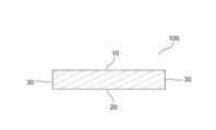
- FIG. 1 is a representative schematic cross-sectional view of a III-nitride semiconductor substrate according to an embodiment of the invention
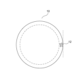
- FIG. 1 is a representative schematic plan view of a group III element nitride semiconductor substrate according to an embodiment of the present invention, viewed from the first surface side
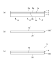
- FIG. It is a schematic explanatory drawing which shows the manufacturing method of the group III element nitride semiconductor substrate by embodiment of this invention.
- 1 is a schematic cross-sectional view showing a cross-sectional structure of a HEMT device including an epitaxial substrate according to an embodiment of the invention
- FIG. 3 is a mapping chart showing the results of mapping measurement of the specific resistance of the wafer (C1) obtained in Comparative Example 1.
- FIG. 10 is a mapping chart showing the results of mapping measurement of the specific resistance of the wafer (C2) obtained in Comparative Example 2.
- FIG. FIG. 10 is a mapping chart showing the result of mapping measurement of the resistivity of the wafer (C3) obtained in Comparative Example 3; 3 is a mapping chart showing the results of mapping measurement of resistivity of wafer (1) obtained in Example 1.
- FIG. FIG. 10 is a mapping chart showing the result of mapping measurement of resistivity of wafer (2) obtained in Example 2;
- FIG. 10 is a mapping chart showing the results of mapping measurement of the resistivity of the wafer (3) obtained in Example 3;
- FIG. 3 is an observation view of a region of the wafer (C1) obtained in Comparative Example 1, which showed low resistance in the measurement of specific resistance, measured with a transmission electron microscope.
- weight When the term “weight” is used in this specification, it may be read as “mass”, which is commonly used as an SI unit indicating weight.
- Group III element nitride semiconductor substrates are typically free-standing substrates made of group III element nitride crystals.
- self-supporting substrate means a substrate that does not deform or break under its own weight during handling and can be handled as a solid object.
- the self-supporting substrate can be used as a substrate for various semiconductor devices such as light emitting elements and power control elements.
- the Group III element nitride semiconductor substrate according to the embodiment of the present invention is typically wafer-shaped (substantially circular). However, if necessary, it may be processed into other shapes such as a rectangular shape.
- any appropriate size can be adopted as the size (diameter) of the group III element nitride semiconductor substrate according to the embodiment of the present invention as long as the effects of the embodiment of the present invention are not impaired.
- Such sizes include, for example, 25 mm (about 1 inch), 45-55 mm (about 2 inches), 95-105 mm (about 4 inches), 145-155 mm (about 6 inches), 195-205 mm (about 8 inches). ), 295-305 mm (about 12 inches), and so on.
- the size (diameter) of the group III element nitride semiconductor substrate according to the embodiment of the present invention is preferably 75 mm or more.
- the group III element nitride semiconductor substrate according to the embodiment of the present invention is a large diameter group III element nitride semiconductor substrate having such a large size (diameter), the group III element nitride semiconductor substrate according to the embodiment of the present invention
- the substrate can be easily applied to high-frequency/high-power electronic devices, and in particular, to devices that handle large power such that the device size is large.
- Group III element nitride semiconductor substrates include 4-inch wafers, 6-inch wafers, 8-inch wafers, and 12-inch wafers.
- the group III element nitride semiconductor substrate according to the embodiment of the present invention preferably has a thickness (thickness at the maximum thickness point if the thickness is not constant) of 100 ⁇ m or more, more preferably 300 ⁇ m to 1000 ⁇ m. be.
- Group III element nitrides typically include gallium nitride (GaN), aluminum nitride (AlN), indium nitride (InN), or mixed crystals thereof. These may be of only one type, or may be of two or more types.
- the Group III element nitride is preferably doped with any one of Fe, Mn, and Zn as a doping element so that the effect of the embodiment of the present invention can be more manifested. Doping with Zn is more preferable from the viewpoint that the resistance value can be easily increased and the in-plane distribution can be made smaller.
- Group III element nitrides may also contain elements other than doping components. Examples of elements include hydrogen (H), oxygen (O), and silicon (Si).
- the plane orientation of the group III element nitride semiconductor substrate can be the c-plane, the m-plane, the a-plane, and specific crystal planes tilted from the c-plane, the a-plane, and the m-plane, particularly the c-plane. In some cases, the effects of the embodiments of the present invention can be more pronounced.
- Specific crystal planes inclined from the c-plane, the a-plane, and the m-plane include so-called semipolar planes such as the ⁇ 11-22 ⁇ plane and the ⁇ 20-21 ⁇ plane.
- plane orientation not only the so-called just plane perpendicular to the c-plane, c-plane, a-plane, m-plane, or a specific crystal plane inclined from these, but also an off angle in the range of ⁇ 5° allowed to contain.
- a group III element nitride semiconductor substrate is a group III element nitride semiconductor substrate having a first surface and a second surface.
- the first surface is the main surface and the second surface is the back surface
- the main surface is typically the group III element polar plane
- the back surface is typically a nitrogen polar surface.
- the main surface may be a nitrogen polar surface
- the rear surface may be a Group III element polar surface.
- Epitaxial crystals can be grown on the main surface, and various devices can be fabricated.
- the back surface can be held by a susceptor or the like to transfer the III-nitride semiconductor substrate according to embodiments of the invention.
- the first surface is the main surface and the second surface is the back surface. Therefore, in this specification, “main surface” may be read as “first surface”, “first surface” may be read as “main surface”, and “back surface” may be read. A thing may be read as a “second side”, and a thing with a “second side” may be read as a "back side”.
- the principal surface may be specular or non-specular.
- the principal surface is a mirror surface.
- the main surface is formed by epitaxially growing the device layer, and the process-affected layer is substantially removed, and the microscopic A surface with a small surface roughness in the region of
- the back surface may be a mirror surface or a non-mirror surface.
- a mirror surface is a surface that has been mirror-finished. After mirror-finishing, the roughness and undulation of the surface are reduced until it is possible to visually confirm that an object is reflected on the mirror-finished surface by reflecting light. refers to the surface in the state of being In other words, it is a surface in which the roughness and undulations of the surface after mirror finishing are sufficiently reduced to the extent that they can be ignored with respect to the wavelength of visible light. Epitaxial crystal growth is sufficiently possible on the mirror-finished surface.
- any appropriate method can be adopted as the method of mirror finishing within the range that does not impair the effects of the embodiments of the present invention.
- a polishing device using a tape for example, a lapping device using diamond abrasive grains, a CMP (Chemical Mechanical Polish) device using a slurry such as colloidal silica and a non-woven polishing pad, etc.
- a method of mirror-finishing using one or a combination thereof can be mentioned. If a work-affected layer remains on the surface after processing, the work-affected layer is typically removed. Methods for removing the work-affected layer include, for example, a method of removing the work-affected layer using RIE (Reactive Ion Etching) or a chemical solution, and a method of annealing the substrate.
- RIE Reactive Ion Etching
- a non-mirror surface is a surface that has not been mirror-finished, and typically includes a rough surface obtained by roughening treatment.
- any appropriate method can be adopted as the roughening treatment method as long as it does not impair the effects of the embodiments of the present invention.
- Examples of such methods include grinding using a grindstone, laser texturing, etching using various chemicals and gases, physical or chemical coating, and texturing by machining.
- FIG. 1 is a representative schematic cross-sectional view of a Group III element nitride semiconductor substrate according to an embodiment of the present invention.
- a Group III element nitride semiconductor substrate 100 according to an embodiment of the present invention typically has a primary surface (III element polar surface) 10 and a back surface (nitrogen polar surface) 20 .
- a III-nitride semiconductor substrate 100 according to embodiments of the present invention may have a side surface 30 .
- the end portion of the group III element nitride semiconductor substrate according to the embodiment of the present invention can take any appropriate form within the range that does not impair the effects of the embodiment of the present invention.
- the end portion of the group III element nitride semiconductor substrate according to the embodiment of the present invention has, for example, a chamfered shape in which the main surface side and the back surface side are flat surfaces, and a shape in which the main surface side and the back surface side are chamfered in an R shape. , a shape in which only the main surface side of the end portion is chamfered to form a flat surface, and a shape in which only the rear surface side of the end portion is chamfered to form a flat surface.
- the chamfered portion may be provided over the entire circumference of the outer circumference, or may be part of the outer circumference. may be provided only in This peripheral portion is typically a region where no devices are formed.
- such an outer peripheral portion is a region extending from the outer peripheral end portion 12 toward the inside of the main surface 10 to a distance of width D1 over the entire circumference.
- the width D1 of the main chamfered portion is the distance starting from the outer peripheral edge 12 and is the distance in the direction normal to the tangent line at the outer peripheral edge 12 toward the inner direction of the main surface 10 .
- the width D1 is preferably constant.
- the width D1 is preferably 5 mm or less, more preferably 4 mm or less, even more preferably 3 mm or less, particularly preferably 2 mm or less, in terms of allowing the effects of the embodiment of the present invention to be more expressed, Most preferably, it is 1 mm or less.
- the lower limit of the width D1 is preferably 0.3 mm or more from the viewpoint that the effect of the embodiment of the present invention can be exhibited more effectively.
- the minimum in-plane resistivity of the first surface is 1 ⁇ 10 7 ⁇ cm or more, preferably 1 ⁇ 10 8 ⁇ cm or more. more preferably 1 ⁇ 10 9 ⁇ cm or more, still more preferably 1 ⁇ 10 10 ⁇ cm or more, and particularly preferably 1 ⁇ 10 11 ⁇ cm or more. If the minimum value of the in-plane resistivity of the first surface of the group III element nitride semiconductor substrate according to the embodiment of the present invention is within the above range, variations in the characteristics of the elements formed on the substrate can be suppressed. .
- the minimum in-plane resistivity of the first surface is 0.01 times or more the maximum in-plane resistivity of the first surface, It is preferably 0.01-fold to 1.0-fold, more preferably 0.1-fold to 1.0-fold, still more preferably 0.5-fold to 1.0-fold, and particularly preferably 0.8-fold. times to 1.0 times. If the magnitude of the minimum to maximum in-plane resistivity of the first surface of the group III element nitride semiconductor substrate according to the embodiment of the present invention is adjusted within the above range, the device formed on the substrate can be Variation in characteristics can be suppressed.
- the inventors of the present invention consider that the in-plane variation in the quality of the semi-insulating GaN free-standing substrate may be the cause of the variation in the characteristics of the conventional GaN-HEMT device, and have investigated the quality of the semi-insulating GaN free-standing substrate. We focused on in-plane variation. As a result of detailed examination of a semi-insulating GaN substrate containing elements with poor characteristics, it was found that there was a problem in the electrical resistivity distribution of the substrate, and that there was a partial region with low resistance. found.
- the minimum value of the in-plane resistivity of the first surface is set to a predetermined range.
- the semi-insulating GaN substrate in which the existence of the low-resistance region is suppressed can be obtained by adjusting and designing by adjusting the magnitude of the minimum value of the resistivity with respect to the maximum value of the resistivity within a predetermined range. The inventors have found that it is possible to suppress variations in the characteristics of elements formed on a substrate.
- the measurement interval in the measurement of the specific resistance is preferably 10 mm or less, more preferably 5 mm or less, still more preferably 4 mm or less, still more preferably 3 mm or less, particularly preferably 2 mm or less, especially It is preferably 1 mm or less.
- the group III element nitride semiconductor substrate according to the embodiment of the present invention preferably has an arbitrary area of 10 mm ⁇ 10 mm, more preferably an arbitrary area of 5 mm ⁇ 5 mm, and even more preferably An arbitrary area of 4 mm ⁇ 4 mm, more preferably an arbitrary area of 3 mm ⁇ 3 mm, particularly preferably an arbitrary area of 2 mm ⁇ 2 mm, particularly preferably an arbitrary area of 1 mm ⁇ 1 mm. is 1 ⁇ 10 7 ⁇ cm or more, and the minimum value of the specific resistance of the arbitrary region is typically 0.01 times or more of the maximum value of the specific resistance of the arbitrary region.
- the minimum resistivity value and the ratio between the minimum resistivity value and the maximum resistivity value are each preferably as described above.
- the specific resistance can be measured by any appropriate method as long as the effects of the embodiments of the present invention are not impaired.
- Methods for measuring such specific resistance include, for example, the capacitance method, the two-terminal method, and the double ring electrode method.
- the two-terminal method and double ring method are destructive measurements.
- the substrate is cut into pieces to match the measurement range, electrodes are formed on the front and back surfaces, and current-voltage measurements are made.
- the resistivity is measured by
- the capacitance method is a non-destructive measurement.
- a probe is used to apply a high voltage from the surface of the substrate without contact while the back surface of the substrate is placed on a conductive stage. Measure the resistivity from At this time, any point on the substrate can be measured by moving the probe or stage in the XY directions.
- the effect of the embodiment of the present invention can be further expressed, so the measurement of the specific resistance is preferable.
- an eddy current method can be used . Not suitable for substrate measurements.
- the measurement of the specific resistance is preferably performed excluding the outer peripheral portion shown in FIG.
- the group III element nitride semiconductor substrate according to the embodiment of the present invention preferably has an oxygen concentration of 2 ⁇ 10 16 atoms/cm 3 to 6 ⁇ 10 16 atoms/cm 3 by SIMS therein, and more preferably 2 ⁇ 10 16 atoms/cm 3 . ⁇ 10 16 atoms/cm 3 to 5 ⁇ 10 16 atoms/cm 3 , more preferably 2 ⁇ 10 16 atoms/cm 3 to 4 ⁇ 10 16 atoms/cm 3 , particularly preferably 2 ⁇ 10 16 atoms/cm 3 . /cm 3 to 3 ⁇ 10 16 atoms/cm 3 .
- the present inventors have found that if the group III element nitride semiconductor substrate is designed by adjusting the oxygen concentration in the group III element nitride semiconductor substrate by SIMS within the above-mentioned predetermined range to suppress the variation, the low resistance region It has been found that a Group III element nitride semiconductor substrate can be obtained in which the presence of is further suppressed, and variations in the characteristics of elements formed on the substrate can be further suppressed. Therefore, if the SIMS oxygen concentration in the group III element nitride semiconductor substrate according to the embodiment of the present invention is within the above range, the variation in the characteristics of the elements formed on the substrate can be further suppressed.
- the Group III element nitride semiconductor substrates according to embodiments of the present invention preferably do not contain nanopipes therein.
- the present inventors have found that if the group III element nitride semiconductor substrate is designed to suppress the presence of nanopipes in the group III element nitride semiconductor substrate, the group III element nitride semiconductor substrate can further suppress the presence of the low resistance region. It has been found that a semiconductor substrate can be obtained, and variations in the characteristics of elements formed on the substrate can be further suppressed. Therefore, if nanopipes are not included in the group III element nitride semiconductor substrate according to the embodiment of the present invention, variations in the characteristics of devices formed on the substrate can be further suppressed. When nanopipes are included in the group III element nitride semiconductor substrate, the effects of the embodiments of the present invention are less likely to be exhibited.
- the Group III element nitride semiconductor substrates according to the embodiments of the present invention can be manufactured by any suitable method as long as the effects of the embodiments of the present invention are not impaired.
- a preferred method for manufacturing a group III element nitride semiconductor substrate according to an embodiment of the present invention will be described in terms of exhibiting the effect of the embodiment of the present invention.
- a group III element nitride layer 3 is formed on the group III element polar plane 2 a of the seed crystal film 2 .
- the group III element nitride layer (seed crystal film 2 + group III element nitride layer 3) to be a free-standing substrate is separated from the base substrate 1 to obtain a free-standing substrate 100' having a main surface 10' and a rear surface 20'.
- any appropriate material can be adopted as the material of the underlying substrate as long as the effects of the embodiments of the present invention are not impaired.
- examples of such materials include sapphire, crystal-oriented alumina, gallium oxide, Al x Ga 1-x N (0 ⁇ x ⁇ 1), GaAs, and SiC.
- any appropriate material can be adopted as the material of the seed crystal film as long as the effects of the embodiments of the present invention are not impaired.
- examples of such materials include Al x Ga 1-x N (0 ⁇ x ⁇ 1) and In x Ga 1-x N (0 ⁇ x ⁇ 1), preferably gallium nitride. More preferably, the material for the seed crystal film is gallium nitride, which has a yellow luminous effect when observed with a fluorescence microscope. Yellow emission is band-to-band exciton transitions (UV) plus peaks appearing in the range 2.2-2.5 eV (yellow emission (YL) or yellow band (YB)).
- UV band-to-band exciton transitions
- YL yellow emission
- YB yellow band
- any appropriate forming method can be adopted as long as the effects of the embodiments of the present invention are not impaired.
- Such formation methods include, for example, a vapor phase epitaxy method, preferably a metal-organic chemical vapor deposition (MOCVD) method, a hydride vapor phase epitaxy (HVPE) method, and a pulse excitation method.
- MOCVD metal-organic chemical vapor deposition
- HVPE hydride vapor phase epitaxy
- PXD deposition
- MBE method MBE method
- sublimation method can be mentioned.
- the MOCVD method is more preferable as the method for forming the seed crystal film.
- the seed crystal film is formed by the MOCVD method, for example, after depositing a low-temperature growth buffer layer of 20 nm to 50 nm at 450° C. to 550° C., laminating a film of 2 ⁇ m to 4 ⁇ m in thickness at 1000° C. to 1200° C. It is preferable to carry out by
- any appropriate growth direction can be adopted as the growth direction of the group III element nitride crystal layer within a range that does not impair the effects of the embodiments of the present invention.
- Such growth directions include, for example, the normal direction of the c-plane of the wurtzite structure, the normal directions of each of the a-plane and m-plane, and the normal directions of planes inclined from each of the c-plane, a-plane and m-plane. mentioned.
- any appropriate method may be used as long as it has a crystal orientation that roughly follows the crystal orientation of the seed crystal film, as long as it does not impair the effects of the embodiments of the present invention.
- Forming methods may be employed. Examples of such formation methods include vapor phase growth methods such as MOCVD, HVPE, PXD, MBE and sublimation; liquid phase growth such as Na flux, ammonothermal, hydrothermal and sol-gel methods; a growth method; a powder growth method using solid-phase growth of powder; a combination thereof; and the like.
- the Na flux method is adopted as the method for forming the group III element nitride crystal layer, the manufacturing method described in Japanese Patent No. 5244628 is followed, and conditions are appropriately adjusted so that the effects of the embodiments of the present invention can be further expressed. It is preferable to perform the Na flux method by adjusting etc.
- Formation of a group III element nitride crystal layer by the Na flux method is typically performed by placing a seed crystal substrate (underlying substrate + seed crystal film) in a crucible as a growth vessel in a nitrogen atmosphere, is filled with a melt composition containing a group III element, metal Na, and a dopant (e.g., Fe, Mn, Zn, etc.), the crucible is covered, and the crucible with the lid is placed in the outer container Then, the outer container is placed in a pressure-resistant container and heated to preferably 700 ° C. to 1000 ° C. (more preferably 800 ° C. to 900 ° C.), preferably 1 MPa to 7 MPa (preferably 2 MPa to 6 MPa) in a nitrogen atmosphere. It is preferable to carry out by rotating while maintaining the temperature and pressure after hot pressurization.
- a seed crystal substrate underlying substrate + seed crystal film
- a crucible as a growth vessel in a nitrogen atmosphere
- At least one selected from Fe, Mn, and Zn is preferably adopted as the dopant, and Zn is more preferably adopted as the dopant, in that the effect of the embodiment of the present invention can be more expressed.
- any appropriate crucible that can be used for the Na flux method can be adopted as the crucible as long as it does not impair the effects of the embodiment of the present invention. It is preferable to adopt an alumina crucible coated with aluminum nitride (AlN) as the above crucible in that the effect of the embodiment of the present invention can be more expressed, and heat treatment is performed after coating with aluminum nitride (AlN). It is more preferable to employ an alumina crucible. In particular, when an alumina crucible that has been heat-treated after being coated with aluminum nitride (AlN) is used, the density of the AlN film is improved by the heat treatment, and contamination with impurities such as oxygen is highly effectively reduced. Therefore, for example, growth starting points of nanopipes are less likely to occur, and the effects of the embodiments of the present invention can be more manifested.
- AlN aluminum nitride
- the above heat treatment can be performed by any appropriate method as long as the effects of the embodiments of the present invention are not impaired.
- the heat treatment is preferably performed in a temperature range of 1500° C. to 1950° C., more preferably 1600° C. to 1850° C., in a nitrogen atmosphere, in that the effects of the embodiments of the present invention can be more expressed.
- Heat treatment is performed for 10 to 90 minutes, more preferably 20 to 60 minutes.
- AlN aluminum nitride
- any appropriate crucible lid that can be used for the Na flux method can be adopted as the crucible lid as long as it does not impair the effects of the embodiment of the present invention. It is preferable to employ an alumina lid coated with aluminum nitride (AlN) as the lid of the crucible, since the effect of the embodiment of the present invention can be further exhibited. By adopting an alumina lid coated with aluminum nitride (AlN), it is possible to highly effectively reduce the contamination of impurities such as oxygen. The effect of the embodiment of can be expressed more.
- the above rotation is typically performed by placing it on a turntable and rotating it around the central axis at a constant cycle.
- the above rotation is performed so that the crystal growth rate of the group III element nitride crystal layer on the seed crystal substrate is preferably 5 ⁇ m/h to 25 ⁇ m/h, more preferably 10 ⁇ m/h to 25 ⁇ m/h. . If the crystal growth rate of the group III element nitride crystal layer on the seed crystal substrate is less than 5 ⁇ m/h, the crystal growth time becomes excessive, which may make it difficult to actually produce the crystal. If the crystal growth rate exceeds 25 ⁇ m/h, there is a risk that the inclusion rate will increase.
- the above rotation is preferably performed by (i) rotating in one direction without reversing, or (ii) repeating a reversing operation of rotating in one direction for 1 minute or more and then rotating in the opposite direction for 1 minute or more, (iii) repeat the intermittent operation of rotating in one direction for 5 seconds or longer, stopping for 0.1 second or longer, and then rotating in the same direction for 5 seconds or longer.
- the crystal growth rate may become too fast and the inclusion rate may increase.
- the above rotation is preferably performed clockwise and counterclockwise at a constant cycle in that the effect of the embodiment of the present invention can be more expressed.
- any appropriate method can be adopted as a method for separating the group III element nitride crystal layer from the underlying substrate as long as the effects of the embodiments of the present invention are not impaired.
- Examples of such a method include, for example, a method of spontaneously separating the group III element nitride crystal layer from the underlying substrate by using the difference in thermal contraction in the cooling step after growing the group III element nitride crystal layer; A method of separating the nitride crystal layer from the underlying substrate by chemical etching, as shown in FIG. Examples include a method of separating the layer from the base substrate by a laser lift-off method, a method of removing the Group III element nitride crystal layer from the base substrate by grinding, and the like.
- a self-supporting substrate containing the group III element nitride crystal layer may be obtained by slicing the group III element nitride crystal layer using a wire saw or the like.
- the group III element nitride crystal layer obtained by the Na flux method in this way is ground with a grindstone or the like to flatten the plate surface, and then the plate surface is smoothed by lapping or the like using diamond abrasive grains. is preferred.
- the outer periphery of the self-supporting substrate is ground to form a circular shape with a desired diameter.
- the size of the freestanding substrate is, for example, 25 mm (about 1 inch), 45 to 55 mm (about 2 inches), 95 to 105 mm (about 4 inches), 145 to 155 mm (about 6 inches), 195 to 205 mm (about 8 inches). ), 295-305 mm (about 12 inches), and so on.
- the size (diameter) of the self-supporting substrate is preferably 75 mm or more.
- Group III element nitride semiconductor substrates include 4-inch wafers, 6-inch wafers, 8-inch wafers, and 12-inch wafers.
- the substrate is thinned to a desired thickness and flattened to obtain a free-standing substrate.
- the thickness of the self-supporting substrate is preferably 100 ⁇ m or more, more preferably 300 ⁇ m to 1000 ⁇ m.
- the outer peripheral edge of the self-supporting substrate is chamfered by grinding to finally obtain the Group III element nitride semiconductor substrate 100 according to the embodiment of the present invention.
- the obtained group III element nitride semiconductor substrate 100 can epitaxially grow crystals on its main surface (group III element polar plane) 10, and the functional layer 4 is formed as shown in FIG. A functional element 5 is obtained.
- 20 is the back surface (nitrogen polar surface).
- Gallium nitride, aluminum nitride, indium nitride, or mixed crystals thereof can be exemplified as epitaxial crystals grown on the group III element nitride semiconductor substrate obtained.
- Specific examples of such epitaxial crystals include GaN, AlN, InN, Ga x Al 1-x N (1>x>0), and Ga x In 1-x N (1>x>0).
- the functional layer provided on the obtained Group III element nitride semiconductor substrate includes a rectifying element, a switching element, a power conversion element, and the like. Further, after providing a functional layer on the group III element polar face of the obtained group III element nitride semiconductor substrate, the nitrogen polar face is processed, for example, by grinding or polishing, thereby obtaining the thickness and thickness distribution of the free-standing substrate. can also be made smaller.
- FIG. 4 is a schematic cross-sectional view showing a cross-sectional structure of a HEMT device 2000 including an epitaxial substrate 1000 according to an embodiment of the invention.
- An epitaxial substrate 1000 according to an embodiment of the present invention comprises a group III element nitride semiconductor substrate 100 according to an embodiment of the present invention, a buffer layer 200, a channel layer 300 and a barrier layer 400.
- the HEMT device 2000 has a source electrode 500, a drain electrode 600 and a gate electrode 700 provided on the epitaxial substrate 1000 (on the barrier layer 400). Note that the thickness ratio of each layer in FIG. 4 does not reflect the actual one.
- the buffer layer 200 is a layer formed on (adjacent to) the first surface of the group III element nitride semiconductor substrate 100 according to the embodiment of the present invention and typically having a thickness of 10 nm to 1000 nm.
- the buffer layer 200 is formed at a temperature similar to that of the channel layer 300 and the barrier layer 400, unlike a so-called low temperature buffer layer which is typically formed at a low temperature of less than 800.degree.
- the buffer layer 200 has a dopant (typically Zn) doped into the group III element nitride semiconductor substrate 100 according to the embodiment of the present invention. It is provided as a diffusion suppression layer that suppresses diffusion to the upper barrier layer 400 .
- the buffer layer 200 preferably consists of at least one selected from AlGaN and AlN.
- the channel layer 300 is a layer formed on (adjacent to) the buffer layer 200 .
- the channel layer 300 is typically formed with a thickness of 50 nm to 5000 nm.
- the channel layer 300 is preferably made of GaN.
- the barrier layer 400 is a layer provided on the opposite side of the buffer layer 200 with the channel layer 300 interposed therebetween.
- the barrier layer 400 is typically formed with a thickness of 2 nm to 40 nm.
- the barrier layer 400 may be formed adjacent to the channel layer 300 as shown in FIG. 4, in which case the interface between both layers is a heterojunction interface.
- a spacer layer (not shown) may be provided between the channel layer 300 and the barrier layer 400.
- the region from the interface between the channel layer 300 and the spacer layer to the interface between the barrier layer 400 and the spacer layer is a hetero layer. It becomes the bonding interface region.
- AlN is preferably used for the spacer layer.
- the barrier layer 400 is preferably made of at least one selected from InAlGaN, InAlN, and AlGaN.
- the formation of the buffer layer 200, the channel layer 300, and the barrier layer 400 is achieved by MOCVD, for example.
- MOCVD metal
- the buffer layer 200 is formed of AlGaN
- the channel layer 300 is formed of GaN
- the barrier layer 4 is formed of AlGaN
- the layer formation by the MOCVD method can be applied to organic materials such as Ga and Al.
- MO metal raw material gases
- TMG, TMA metal raw material gases
- ammonia gas ammonia gas
- hydrogen gas hydrogen gas
- nitrogen gas nitrogen gas
- a GaN crystal or an AlGaN crystal generated by a vapor phase reaction between an organometallic raw material gas corresponding to each layer and an ammonia gas is formed according to the embodiment of the present invention.
- the source electrode 500 and the drain electrode 600 are typically metal electrodes each having a thickness of ten and several nanometers to one hundred and several ten nanometers.
- the source electrode 500 and the drain electrode 600 are preferably formed as multi-layered electrodes made of Ti/Al/Ni/Au, for example.
- Source electrode 500 and drain electrode 600 have ohmic contact with barrier layer 400 .
- a preferred example of the source electrode 500 and the drain electrode 600 is formed by a vacuum deposition method and a photolithography process. In order to improve the ohmic contact between both electrodes, it is preferable to perform heat treatment for several tens of seconds in a nitrogen gas atmosphere at a predetermined temperature between 650° C. and 1000° C. after forming the electrodes.
- the gate electrode 700 is typically a metal electrode having a thickness of ten and several nanometers to one hundred and several ten nanometers.
- the gate electrode 700 is preferably configured as a multi-layered electrode made of Ni/Au, for example.
- Gate electrode 700 has a Schottky contact with barrier layer 400 .
- a preferred example of the gate electrode 700 is formed by a vacuum deposition method and a photolithography process.
- the epitaxial substrate 1000 is formed by placing the group III element nitride semiconductor substrate 100 according to the embodiment of the present invention on a susceptor provided in a reactor of an MOCVD furnace, and forming a buffer layer 200 and a channel layer 300 under the following conditions. , and the barrier layer 400 in this order.
- the forming temperature means the susceptor heating temperature.
- the Group 15/Group 13 gas ratio means the total supply of TMG (trimethylgallium), TMA (trimethylaluminum), and TMI (trimethylindium), which are Group 13 (Ga, Al, In) raw materials. It is the ratio (molar ratio) of the supply amount of ammonia, which is a group 15 (N) raw material, to the amount. Further, when the barrier layer 400 is formed of AlGaN, the Al raw material gas/Group 13 raw material gas ratio is the ratio (molar ratio) of the supply amount of the Al raw material to the total supply amount of the Group 13 (Ga, Al) raw material.
- the In raw material gas/group 13 raw material gas ratio when the barrier layer 400 is formed of InAlN is the ratio (molar ratio) of the supply amount of the In raw material to the total supply amount of the group 13 (In, Al) raw material. be. In either case, it is determined according to the desired composition of the barrier layer 400 (Al molar ratio x or In composition ratio y).
- Fabrication of the HEMT device 2000 can be realized by using the epitaxial substrate 1000 according to the embodiment of the present invention and applying known techniques.
- the surface of the epitaxial substrate 1000 (barrier layer A SiO 2 film having a thickness of 50 nm to 500 nm is formed on the surface of the electrode 400), and then the SiO 2 film is removed by etching using photolithography at locations where the source electrode 500 and the drain electrode 600 are to be formed. Obtain a pattern layer.
- each metal layer is in the range 5 nm to 50 nm, 40 nm to 400 nm, 4 nm to 40 nm, and 20 nm to 200 nm, respectively.
- heat treatment is preferably performed in a nitrogen gas atmosphere at 600° C. to 1000° C. for 10 seconds to 1000 seconds.
- a photolithography process is used to remove the SiO 2 film from the SiO 2 pattern layer at the portion where the gate electrode 700 is to be formed.
- the gate electrode 700 is formed by forming a Schottky metal pattern made of Ni/Au at the location where the gate electrode 700 is to be formed using a vacuum deposition method and a photolithography process.
- the thickness of each metal layer is preferably in the range of 4 nm to 40 nm and in the range of 20 nm to 200 nm.
- the HEMT device 2000 is obtained through the above process.
- the oxygen concentration was measured from the main surface (first surface) of the substrate using secondary ion mass spectrometry (SIMS).
- SIMS secondary ion mass spectrometry
- a seed crystal substrate made of gallium nitride and having a thickness of 2 ⁇ m was formed by MOCVD on a sapphire substrate having a diameter of 3 inches to obtain a seed crystal substrate.
- the obtained seed crystal substrate was placed in an AlN-coated alumina crucible in a nitrogen atmosphere glove box.
- metallic gallium and metallic sodium as raw materials and granular manganese as a doping material were filled in the crucible, and the crucible was covered with an AlN-coated alumina lid.
- the crucible with the lid was placed in a stainless steel inner container, further placed in a stainless steel outer container capable of containing it, and closed with a container lid fitted with a nitrogen introduction pipe.
- This outer container was placed on a turntable installed in the heating section of the crystal manufacturing apparatus which had been vacuum-baked in advance, and the pressure-resistant container was closed with a lid.
- the inside of the pressure vessel was evacuated to 0.1 Pa or less by a vacuum pump.
- nitrogen gas was introduced from the nitrogen gas cylinder to 4.0 MPa, and the outer container was rotated around the central axis.
- the gallium nitride crystal was attached to a ceramic processing surface plate, and the Ga polar surface was ground and polished using a grinder and a lapping device. Diamond abrasive grains with a grain size of 0.1 ⁇ m were used for the final finish, and mirror finishing was performed.
- the gallium nitride crystal was turned upside down and fixed on a ceramic processing table, and the nitrogen polar surface was ground and polished in the same manner. Diamond abrasive grains with a grain size of 0.1 ⁇ m were used for the final finish, and mirror finishing was performed.
- a wafer (C1) as a free-standing gallium nitride substrate was produced by the above production method. The specific resistance of the wafer (C1) at room temperature was measured by the capacitance method.
- the specific resistance was measured by mapping 277 points at intervals of 4 mm within the main surface.
- the resistivity varies greatly within the main surface, with a minimum value of 1.0 ⁇ 10 5 ⁇ cm (lower limit of measurement) and a maximum value of 1.1 ⁇ 10 9 ⁇ cm. , 9.1 ⁇ 10 ⁇ 5 .
- FIG. 5 shows the results of mapping measurements of resistivity.
- the oxygen concentrations were 1 ⁇ 10 17 atoms/cm 3 and 2 ⁇ 10 17 atoms/cm 3 , respectively.
- the oxygen concentration was 4 ⁇ 10 16 atoms/cm 3 .
- Comparative Example 2 Under the same conditions as in Comparative Example 1, a wafer (C2) was produced as a gallium nitride free-standing substrate using granular zinc as the doping material. The specific resistance of the wafer (C2) at room temperature was measured by the capacitance method. The specific resistance was measured by mapping 277 points at intervals of 4 mm within the main surface. The resistivity varies greatly within the main surface, with a minimum value of 1.0 ⁇ 10 5 ⁇ cm (lower measurement limit) and a maximum value of 8.6 ⁇ 10 11 ⁇ cm. , 1.2 ⁇ 10 ⁇ 7 . FIG. 6 shows the results of mapping measurements of resistivity.
- SIMS Secondary Ion Mass Spectrometry
- Comparative Example 3 Under the same conditions as in Comparative Example 1, a wafer (C3) was produced as a gallium nitride free-standing substrate using granular iron as the doping material. The specific resistance of the wafer (C3) at room temperature was measured by the capacitance method. The specific resistance was measured by mapping 277 points at intervals of 4 mm within the main surface. The resistivity varies greatly within the main surface, with a minimum value of 1.0 ⁇ 10 5 ⁇ cm (lower measurement limit) and a maximum value of 1.2 ⁇ 10 8 ⁇ cm. , 8.3 ⁇ 10 ⁇ 4 .
- FIG. 7 shows the results of mapping measurements of resistivity.
- SIMS Secondary ion mass spectrometry
- Example 1 A seed crystal substrate made of gallium nitride and having a thickness of 2 ⁇ m was formed by MOCVD on a sapphire substrate having a diameter of 3 inches to obtain a seed crystal substrate.
- the obtained seed crystal substrate was placed in an alumina crucible which had been heat-treated and washed with hydrofluoric acid after being coated with AlN in a glove box in a nitrogen atmosphere. The heat treatment was held at 1700° C. for 30 minutes in a nitrogen atmosphere.
- metallic gallium and metallic sodium as raw materials and granular manganese as a doping material were filled in the crucible, and the crucible was covered with an AlN-coated alumina lid.
- the crucible with the lid was placed in a stainless steel inner container, further placed in a stainless steel outer container capable of containing it, and closed with a container lid fitted with a nitrogen introduction pipe.
- This outer container was placed on a turntable installed in the heating section of the crystal manufacturing apparatus which had been vacuum-baked in advance, and the pressure-resistant container was closed with a lid.
- the inside of the pressure vessel was evacuated to 0.1 Pa or less by a vacuum pump.
- the gallium nitride crystal on the seed crystal substrate was decomposed by irradiating the ultraviolet laser from the sapphire substrate side, and the grown gallium nitride crystal was separated from the sapphire substrate.
- the outer peripheral portion of the separated gallium nitride crystal was ground using a diamond whetstone to adjust the diameter to 75 mm.
- the gallium nitride crystal was attached to a ceramic processing surface plate, and the Ga polar surface was ground and polished using a grinder and a lapping device. Diamond abrasive grains with a grain size of 0.1 ⁇ m were used for the final finish, and mirror finishing was performed.
- the gallium nitride crystal was turned upside down and fixed on a ceramic processing table, and the nitrogen polar surface was ground and polished in the same manner. Diamond abrasive grains with a grain size of 0.1 ⁇ m were used for the final finish, and mirror finishing was performed.
- a wafer (1) as a free-standing gallium nitride substrate was produced by the above production method. The specific resistance of the wafer (1) at room temperature was measured by the capacitance method. The specific resistance was measured by mapping 277 points at intervals of 4 mm within the main surface. A specific resistance of 1 ⁇ 10 7 ⁇ cm or more was obtained over the entire surface.
- Example 2 Under the same conditions as in Example 1, a wafer (2) was produced as a gallium nitride free-standing substrate using granular zinc as the doping material. The specific resistance of the wafer (2) at room temperature was measured by the capacitance method. The specific resistance was measured by mapping 277 points at intervals of 4 mm within the main surface. A specific resistance of 1 ⁇ 10 7 ⁇ cm or more was obtained over the entire surface. The minimum value was 7.1 ⁇ 10 11 ⁇ cm, the maximum value was 9.2 ⁇ 10 11 ⁇ cm, and the minimum/maximum value was 0.77.
- FIG. 9 shows the results of mapping measurements of resistivity.
- Example 3 Under the same conditions as in Example 1, a wafer (3) was produced as a gallium nitride free-standing substrate using granular iron as the doping material. The specific resistance of the wafer (3) at room temperature was measured by the capacitance method. The specific resistance was measured by mapping 277 points at intervals of 4 mm within the main surface. A specific resistance of 1 ⁇ 10 7 ⁇ cm or more was obtained over the entire surface. The minimum value was 1.1 ⁇ 10 7 ⁇ cm, the maximum value was 1.4 ⁇ 10 8 ⁇ cm, and the minimum/maximum value was 0.079.
- FIG. 10 shows the results of mapping measurements of resistivity.
- the oxygen concentration was 3 ⁇ 10 16 atoms / cm 3 , 6 ⁇ 10 16 atoms/cm 3 and 5 ⁇ 10 16 atoms/cm 3 .
- the formation temperature means the susceptor heating temperature
- the Group 15/Group 13 gas ratio refers to TMG (trimethylgallium), TMA (trimethylaluminum), and TMI ( It is the ratio (molar ratio) of the supply amount of ammonia, which is a group 15 (N) raw material, to the total supply amount of trimethylindium).
- the Al raw material gas/Group 13 raw material gas ratio when forming AlGaN is the ratio (molar ratio) of the supply amount of the Al raw material to the total supply amount of the Group 13 (Ga, Al) raw material.
- the main surface of each epitaxial substrate was removed by etching to a depth of about 100 nm at the boundary between each element using the photolithography process and the RIE method.
- the boundary interval was set to 1 mm.
- electrodes made of Ti/Al/Ni/Au were applied to the portions where the source electrode and the drain electrode were to be formed, using a photolithography process and a vacuum deposition method. formed a pattern.
- heat treatment was performed at 800° C. for 30 seconds in nitrogen.
- a pattern of a gate electrode was formed on the upper surface of each epitaxial substrate at a target portion for forming the gate electrode using a photolithography process and a vacuum deposition method.
- Ni/Au film thickness 6 nm/12 nm
- the gate electrode was formed to have a gate length of 1 ⁇ m, a gate width of 100 ⁇ m, a distance of 1 ⁇ m from the source electrode, and a distance of 10 ⁇ m from the drain electrode.
- a HEMT device was obtained by the above process. The device breakdown voltage of the obtained HEMT device was evaluated.
- Some of the HEMT elements formed on the wafers (C1) to (C3), which are gallium nitride self-supporting substrates, produced in Comparative Examples 1 to 3 had a Vdb lower than 300 V, and were evaluated as "poor". .
- Vdb was 300 V or more in all devices, and the evaluation was "Good". Met.
- Group III element nitride semiconductor substrates according to embodiments of the present invention can be used as substrates for various semiconductor devices.
- Group III element nitride semiconductor substrate 100' Self-supporting substrate 1 Base substrate 1a Main surface 1b of base substrate 1 Rear surface 2 of base substrate 1 Seed crystal film 2a Group III element polar surface 3 of seed crystal film 2 Group III element nitride layer 4 functional layer 5 functional element 10 main surface 10 ′ main surface 12 outer peripheral edge 20 back surface 20 ′ back surface 22 outer peripheral edge 30 side surface 1000 epitaxial substrate 2000 HEMT element 200 buffer layer 300 channel layer 400 barrier layer 500 source electrode 600 drain electrode 700 gate electrode
Landscapes
- Junction Field-Effect Transistors (AREA)
- Crystals, And After-Treatments Of Crystals (AREA)
Abstract
第一面と第二面とを備えるIII族元素窒化物半導体基板であって、該基板上に形成された素子の特性のバラツキを抑制できるIII族元素窒化物半導体基板が提供される。本発明の実施形態によるIII族元素窒化物半導体基板は、第一面と第二面とを備えるIII族元素窒化物半導体基板であって、該第一面の面内の比抵抗の最小値が1×107cmΩ以上であり、該第一面の面内の比抵抗の最小値が該第一面の面内の比抵抗の最大値の0.01倍以上である。
Description
本発明はIII族元素窒化物半導体基板に関する。より詳細には、表裏の関係にある主面と裏面とを備えるIII族元素窒化物半導体基板であって、該基板上に形成された素子の特性のバラツキを抑制できるIII族元素窒化物半導体基板に関する。
窒化物半導体は、直接遷移型の広いバンドギャップを有し、高い絶縁破壊電界、高い飽和電子速度を有することから、LEDやLDなどの発光デバイスや、高周波/ハイパワーの電子デバイス用半導体材料などに広く適用されている。
窒化物電子デバイスの代表的な構造として、自立GaN基板上に、AlGaNを「障壁層」、GaNを「チャネル層」として積層形成した、高電子移動度トランジスタ(HEMT)構造が知られている。これは、窒化物材料特有の大きな分極効果(自発分極効果とピエゾ分極効果)によりAlGaN/GaN積層界面に高濃度の2次元電子ガスが生成するという特徴を活かしたものである。
窒化物電子デバイスは、一般的に、サファイア、SiC、Siといった、商業的に入手の容易な異種材料下地基板を用いて作製されている。しかしながら、これら異種材料基板上にヘテロエピタキシャル成長させたGaN膜中には、GaNと異種材料基板との間の格子定数や熱膨張係数の差異に起因して、多数の欠陥が発生してしまうという問題がある。
一方、GaN基板上にGaN膜をホモエピタキシャル成長させた場合、上記の格子定数や熱膨張係数の差異に起因する欠陥は発生せず、GaN膜は良好な結晶性を示す。それゆえ、GaN基板上に窒化物HEMT構造を作製した場合、AlGaN/GaN積層界面に存在する2次元電子ガスの移動度が向上するので、当該構造を用いて作製するHEMT素子(半導体素子)の特性向上が期待できる。
ところが、商業的に入手が可能である、ハイドライド気相成長法(HVPE法)にて作製されたGaN基板は、一般的には、結晶内に取り込んだ酸素不純物のためn型の伝導型を呈する。導電性のGaN基板は、HEMT素子を高電圧駆動した際に、ソース-ドレイン電極間のリーク電流経路となる。そのため、HEMT素子を作製するには、半絶縁性GaN基板の採用が望ましい。
半絶縁性GaN基板を得るためには、深いアクセプター準位を形成する元素をGaN結晶中にドーピングすることが有効である。
半絶縁性自立GaN基板として、ドーピング元素としてFe、Mn、Znなどを含む基板が報告されている(特許文献1-5)。しかし、これらの半絶縁性自立GaN基板は、その上にHEMTを作製してGaN-HEMTとした場合、一部のHEMT素子でリーク電流が増加して耐圧が低下するなどして、HEMT素子の特性にバラツキが見られることがあり、十分に高い特性のHEMT素子を提供するまでには至っていない。
本発明の課題は、第一面と第二面とを備えるIII族元素窒化物半導体基板であって、該基板上に形成された素子の特性のバラツキを抑制できるIII族元素窒化物半導体基板を提供することにある。
[1]本発明の実施形態によるIII族元素窒化物半導体基板は、第一面と第二面とを備えるIII族元素窒化物半導体基板である。該基板は、該第一面の面内の比抵抗の最小値が1×10⁷Ω・cm以上であり、該第一面の面内の比抵抗の最小値が該第一面の面内の比抵抗の最大値の0.01倍以上である。
[2]上記[1]において、上記比抵抗の測定は、測定間隔10mm以下で連続的に行われる。
[3]上記[1]または[2]において、上記比抵抗の測定は、電気容量法による前記第一面の面内のマッピング測定によって行われる。
[4]上記[1]から[3]のいずれかにおいて、上記III族元素窒化物半導体基板は、ドーパントとしてZnを含む。
[5]上記[1]から[4]のいずれかにおいて、上記III族元素窒化物半導体基板中のSIMSによる酸素濃度は2×10¹⁶atoms/cm3~6×1016atoms/cm3である。
[6]上記[1]から[5]のいずれかにおいて、上記III族元素窒化物半導体基板中にナノパイプを含まない。
[7]上記[1]から[6]のいずれかにおいて、上記III族元素窒化物半導体基板は、直径が75mm以上である。
[8]本発明の別の局面においては、エピタキシャル基板が提供される。該エピタキシャル基板は、上記[1]から[7]のいずれかのIII族元素窒化物半導体基板の第一面上に、AlGaNおよびAlNから選ばれる少なくとも1種からなるバッファ層と、GaNからなるチャネル層と、InAlGaN、InAlN、およびAlGaNから選ばれる少なくとも1種からなる障壁層と、をこの順に備える。
[9]本発明のさらに別の局面においては、機能素子が提供される。該機能素子は、上記[1]から[7]のいずれかのIII族元素窒化物半導体基板の第一面上に、AlGaNおよびAlNから選ばれる少なくとも1種からなるバッファ層と、GaNからなるチャネル層と、InAlGaN、InAlN、およびAlGaNから選ばれる少なくとも1種からなる障壁層と、をこの順に備える。
本発明によれば、第一面と第二面とを備えるIII族元素窒化物半導体基板であって、該基板上に形成された素子の特性のバラツキを抑制できるIII族元素窒化物半導体基板を提供することができる。
本明細書中で「重量」との表現がある場合は、重さを示すSI系単位として慣用されている「質量」と読み替えてもよい。
≪III族元素窒化物半導体基板≫
本発明の実施形態によるIII族元素窒化物半導体基板は、代表的には、III族元素窒化物結晶からなる自立基板である。本明細書において、「自立基板」とは、取り扱う際に自重で変形または破損せず、固形物として取り扱うことのできる基板を意味する。自立基板は発光素子や電力制御素子等の各種半導体デバイスの基板として使用可能である。
本発明の実施形態によるIII族元素窒化物半導体基板は、代表的には、III族元素窒化物結晶からなる自立基板である。本明細書において、「自立基板」とは、取り扱う際に自重で変形または破損せず、固形物として取り扱うことのできる基板を意味する。自立基板は発光素子や電力制御素子等の各種半導体デバイスの基板として使用可能である。
本発明の実施形態によるIII族元素窒化物半導体基板は、代表的には、ウエハー状(略真円状)である。しかし、必要に応じて、それ以外の形状、例えば、矩形等の形状に加工してもよい。
本発明の実施形態によるIII族元素窒化物半導体基板のサイズ(直径)としては、本発明の実施形態による効果を損なわない範囲で、任意の適切なサイズを採用し得る。このようなサイズとしては、例えば、25mm(約1インチ)、45~55mm(約2インチ)、95~105mm(約4インチ)、145~155mm(約6インチ)、195~205mm(約8インチ)、295~305mm(約12インチ)等である。本発明の実施形態によるIII族元素窒化物半導体基板のサイズ(直径)としては、好ましくは75mm以上である。本発明の実施形態によるIII族元素窒化物半導体基板が、このようにサイズ(直径)が大きい大口径のIII族元素窒化物半導体基板であると、本発明の実施形態によるIII族元素窒化物半導体基板は、高周波/ハイパワーの電子デバイスへの適用が容易になり、特に、素子サイズが大きくなるような大電力を扱うデバイスへの適用が容易になる。
大口径のIII族元素窒化物半導体基板としては、具体的には、例えば、4インチウエハー、6インチウエハー、8インチウエハー、12インチウエハーなどが挙げられる。
本発明の実施形態によるIII族元素窒化物半導体基板は、その厚さ(厚さが一定でない場合は最大厚さ箇所の厚さ)が、好ましくは100μm以上であり、より好ましくは300μm~1000μmである。
III族元素窒化物としては、代表的には、窒化ガリウム(GaN)、窒化アルミニウム(AlN)、窒化インジウム(InN)またはこれらの混晶が挙げられる。これらは、1種のみであってもよいし、2種以上であってもよい。
III族元素窒化物は、具体的には、GaN、AlN、InN、GaxAl1-xN(1>x>0)、GaxIn1-xN(1>x>0)、AlxIn1-xN(1>x>0)、GaxAlyInzN(1>x>0、1>y>0、x+y+z=1)である。
本発明の実施形態による効果をより発現させ得る点で、III族元素窒化物は、好ましくは、ドーピング元素としてFe、Mn、Znのいずれかでドープされている。抵抗値を高めやすく、面内分布をより小さくできる観点で、Znをドープことがより好ましい。また、III族元素窒化物は、ドープ成分以外の元素を含み得る。元素としては、例えば、水素(H)、酸素(O)、シリコン(Si)などが挙げられる。
III族元素窒化物半導体基板の面方位は、c面、m面、a面、およびc面、a面、m面それぞれから傾斜した特定の結晶面とすることができ、特に、c面とした際に本発明の実施形態による効果がより発現され得る。c面、a面、m面それぞれから傾斜した特定の結晶面としては、{11-22}面や{20-21}面といった、いわゆる半極性面が例示できる。また、面方位としては、c面、c面、a面、m面あるいはこれらから傾斜した特定の結晶面に対して、垂直ないわゆるジャスト面だけでなく、±5°の範囲でのオフ角を含むことが許容される。
本発明の実施形態によるIII族元素窒化物半導体基板は、第一面と第二面とを備えるIII族元素窒化物半導体基板である。第一面を主面、第二面を裏面としたとき、III族元素窒化物半導体基板の面方位がc面であれば、主面は、代表的には、III族元素極性面であり、裏面は、代表的には、窒素極性面である。しかしながら、主面を窒素極性面としてもよいし、裏面をIII族元素極性面としてもよい。主面上には、エピタキシャル結晶を成長させることができ、また、各種デバイスを作製することができる。裏面は、サセプタなどによって保持させて、本発明の実施形態によるIII族元素窒化物半導体基板を移送できる。
本発明の実施形態によるIII族元素窒化物半導体基板の説明においては、第一面を主面、第二面を裏面として説明する。したがって、本明細書において、「主面」とあるものは「第一面」と読み替えてもよく、「第一面」とあるものは「主面」と読み替えてもよく、「裏面」とあるものは「第二面」と読み替えてもよく、「第二面」とあるものは「裏面」と読み替えてもよい。
主面は、鏡面であっても非鏡面であってもよい。好ましくは、主面は鏡面である。
主面は、デバイス層をエピタキシャル成長させて、作製するデバイスの特性が良好で、デバイス間のデバイス特性のバラツキの少ない半導体デバイスを得る観点からは、加工変質層が実質的に除去され、かつ、ミクロな領域での表面粗さが小さい面が好ましい。
裏面は、鏡面であっても非鏡面であってもよい。
鏡面とは、鏡面加工された表面であり、鏡面加工後に、光が反射して鏡面加工された表面上に物が映っていることを目視で確認することができるまで表面の粗さやうねりが低減されている状態の表面を指す。つまり、鏡面加工後の表面の粗さやうねりの大きさが、可視光の波長に対して十分無視できる程度にまで低減されている状態の表面である。鏡面加工されている表面上にはエピタキシャル結晶成長が十分可能である。
鏡面加工の方法としては、本発明の実施形態による効果を損なわない範囲で、任意の適切な方法を採用し得る。このような方法としては、例えば、テープを用いた研磨装置、ダイヤモンド砥粒を用いたラッピング装置、コロイダルシリカ等のスラリーと不織布の研磨パッドとを用いたCMP(Chemical Mechanical Polish)装置などを、1つまたは組み合わせて用いて鏡面加工する方法などが挙げられる。加工後の表面に加工変質層が残る場合は、代表的には加工変質層を除去する。加工変質層を除去する方法としては、例えば、RIE(Reactive Ion Etching:反応性イオンエッチング)や薬液を用いて加工変質層を除去する方法、基板をアニールする方法、などが挙げられる。
非鏡面とは、鏡面加工されていない表面であり、代表的には、粗面化処理によって得られる粗面が挙げられる。
粗面化処理の方法としては、本発明の実施形態による効果を損なわない範囲で、任意の適切な方法を採用し得る。このような方法としては、例えば、砥石を用いた研削加工、レーザテクスチャ加工、各種薬液やガスを用いたエッチング処理、物理的あるいは化学的なコーティング処理、機械加工によるテクスチャリングなどが挙げられる。
図1は、本発明の実施形態によるIII族元素窒化物半導体基板の代表的な概略断面図である。図1に示すように、本発明の実施形態によるIII族元素窒化物半導体基板100は、代表的には、主面(III族元素極性面)10と裏面(窒素極性面)20を有する。本発明の実施形態によるIII族元素窒化物半導体基板100は、側面30を有していてもよい。
本発明の実施形態によるIII族元素窒化物半導体基板の端部は、本発明の実施形態による効果を損なわない範囲で、任意の適切な形態を採り得る。本発明の実施形態によるIII族元素窒化物半導体基板の端部は、例えば、主面側と裏面側が平坦面となるように面取りされた形状、主面側と裏面側がR状に面取りされた形状、端部の主面側だけが平坦面となるように面取りされている形状、端部の裏面側だけが平坦面となるように面取りされている形状などが挙げられる。
本発明の実施形態によるIII族元素窒化物半導体基板の端部が面取りされている場合、その面取りされた部分は、外周部の1周全部にわたって設けられていてよく、あるいは、外周部の一部のみに設けられていてもよい。この外周部は、代表的には、デバイスの形成を行わない領域である。
図2に示すように、このような外周部は、全周にわたって外周端部12から主面10の内側方向に向かって幅D1の距離までの領域である。主面面取り部の幅D1は、外周端部12を起点とする距離であって、主面10の内側方向に向かって、該外周端部12における接線に対する法線方向の距離である。幅D1は一定であることが好ましい。
幅D1は、本発明の実施形態による効果を損なわない範囲で、任意の適切な大きさを採用し得る。本発明の実施形態による効果をより発現させ得る点で、幅D1は、好ましくは5mm以下であり、より好ましくは4mm以下であり、さらに好ましくは3mm以下であり、特に好ましくは2mm以下であり、最も好ましくは1mm以下である。幅D1の下限値は、本発明の実施形態による効果をより発現させ得る点で、好ましくは0.3mm以上である。
本発明の実施形態によるIII族元素窒化物半導体基板は、第一面の面内の比抵抗の最小値が1×10⁷Ω・cm以上であり、好ましくは1×10⁸Ω・cm以上であり、より好ましくは1×10⁹Ω・cm以上であり、さらに好ましくは1×10¹⁰Ω・cm以上であり、特に好ましくは1×10¹¹Ω・cm以上である。本発明の実施形態によるIII族元素窒化物半導体基板の第一面の面内の比抵抗の最小値が上記範囲内にあれば、該基板上に形成された素子の特性のバラツキを抑制し得る。
本発明の実施形態によるIII族元素窒化物半導体基板は、第一面の面内の比抵抗の最小値が該第一面の面内の比抵抗の最大値の0.01倍以上であり、好ましくは0.01倍~1.0倍であり、より好ましくは0.1倍~1.0倍であり、さらに好ましくは0.5倍~1.0倍であり、特に好ましくは0.8倍~1.0倍である。本発明の実施形態によるIII族元素窒化物半導体基板の第一面の面内の比抵抗の最小値の最大値に対する大きさを上記の範囲に調整すれば、該基板上に形成された素子の特性のバラツキを抑制し得る。
本発明者らは、従来のGaN-HEMT素子の特性のバラツキの原因として、半絶縁性のGaN自立基板の品質の面内バラツキの可能性を考え、この半絶縁性のGaN自立基板の品質の面内バラツキに着目した。そして、特性の悪い素子が含まれた半絶縁性のGaN基板について詳細に調べた結果、該基板の電気抵抗率分布に問題があることが判明し、部分的に抵抗の低い領域があることが判明した。そこで、さらに検討を進めたところ、上記のように、第一面と第二面とを備える半絶縁性のGaN基板について、その第一面の面内の比抵抗の最小値を所定の範囲に調整し、かつ、該比抵抗の最小値の最大値に対する大きさを所定の範囲に調整して設計すれば、低抵抗領域の存在を抑制した半絶縁性のGaN基板を得ることができ、該基板上に形成された素子の特性のバラツキを抑制できることを見出した。
上記比抵抗の測定における測定間隔は、好ましくは10mm以下であり、より好ましくは5mm以下であり、さらに好ましくは4mm以下であり、さらに好ましくは3mm以下であり、特に好ましくは2mm以下であり、とりわけ好ましくは1mm以下である。上記比抵抗の測定における測定間隔を上記範囲にすれば、本発明の実施形態によるIII族元素窒化物半導体基板上に形成された素子の特性のバラツキをより抑制し得る。言い換えれば、本発明の実施形態によるIII族元素窒化物半導体基板は、第一面の面内において、好ましくは10mm×10mmの任意の領域、より好ましくは5mm×5mmの任意の領域、さらに好ましくは4mm×4mmの任意の領域、さらに好ましくは3mm×3mmの任意の領域、特に好ましくは2mm×2mmの任意の領域、とりわけ好ましくは1mm×1mmの任意の領域の比抵抗の最小値が代表的には1×10⁷Ω・cm以上であり、当該任意の領域の比抵抗の最小値が、代表的には当該任意の領域の比抵抗の最大値の0.01倍以上である。比抵抗の最小値、および、比抵抗の最小値と最大値との比は、それぞれ、好ましくは上記のとおりである。
上記比抵抗の測定は、本発明の実施形態による効果を損なわない範囲で、任意の適切な方法で測定し得る。このような比抵抗の測定方法としては、例えば、電気容量法、二端子法、二重リング電極法が挙げられる。
二端子法および二重リング法は破壊測定であり、代表的には、基板を測定範囲に合わせた大きさに切断することで個片化し、表面および裏面に電極を形成した後に電流―電圧測定をすることで比抵抗を測定する。
電気容量法は非破壊測定であり、代表的には、基板の裏面を導電性ステージに設置した状態でプローブにより基板の表面から非接触で高電圧を印加し、電気容量測定による電荷の過渡応答から比抵抗を測定する。この際、プローブまたはステージをXY方向に移動させることで基板の任意の点の測定が可能である。
非接触式の比抵抗測定であること、および、基板面内の比抵抗分布を的確に把握できることから、本発明の実施形態による効果をより発現させ得る点で、上記比抵抗の測定は、好ましくは、電気容量法による第一面の面内のマッピング測定によって行われる。マッピング測定は、代表的には、プローブをXY方向に移動させて行う。
なお、非接触式の比抵抗測定として、渦電流法も挙げられるが、比抵抗の測定範囲が10-3Ω・cm~102Ω・cmであり、半絶縁性のIII族元素窒化物半導体基板の測定には適していない。
上記比抵抗の測定は、本発明の実施形態による効果をより発現させ得る点で、好ましくは、前述した、図2に示す外周部を除いて行う。
本発明の実施形態によるIII族元素窒化物半導体基板は、その中のSIMSによる酸素濃度が、好ましくは2×10¹⁶atoms/cm3~6×1016atoms/cm3であり、より好ましくは2×1016atoms/cm3~5×1016atoms/cm3であり、さらに好ましくは2×1016atoms/cm3~4×1016atoms/cm3であり、特に好ましくは2×1016atoms/cm3~3×1016atoms/cm3である。本発明者らは、III族元素窒化物半導体基板の中のSIMSによる酸素濃度を上記の所定範囲内に調整してバラツキを抑制してIII族元素窒化物半導体基板を設計すれば、低抵抗領域の存在をより抑制したIII族元素窒化物半導体基板を得ることができ、該基板上に形成された素子の特性のバラツキをより抑制できることを見出した。したがって、本発明の実施形態によるIII族元素窒化物半導体基板の中のSIMSによる酸素濃度が上記範囲内にあれば、該基板上に形成された素子の特性のバラツキをより抑制し得る。
本発明の実施形態によるIII族元素窒化物半導体基板は、好ましくは、その中にナノパイプを含まない。本発明者らは、III族元素窒化物半導体基板の中のナノパイプの存在を抑制するようにIII族元素窒化物半導体基板を設計すれば、低抵抗領域の存在をより抑制したIII族元素窒化物半導体基板を得ることができ、該基板上に形成された素子の特性のバラツキをより抑制できることを見出した。したがって、本発明の実施形態によるIII族元素窒化物半導体基板の中にナノパイプが含まれなければ、該基板上に形成された素子の特性のバラツキをより抑制し得る。III族元素窒化物半導体基板の中にナノパイプが含まれると、本発明の実施形態による効果が発現されにくくなる。
本発明の実施形態によるIII族元素窒化物半導体基板は、本発明の実施形態による効果を損なわない範囲で、任意の適切な方法で製造し得る。以下、本発明の実施形態による効果をより発現させる点で、本発明の実施形態によるIII族元素窒化物半導体基板の好ましい製造方法について説明する。
本発明の実施形態によるIII族元素窒化物半導体基板の製造方法においては、代表的には、図3(a)に示すように、下地基板1の主面1a上に種結晶膜2を形成し、種結晶膜2のIII族元素極性面2a上にIII族元素窒化物層3を形成する。次いで、下地基板1から自立基板となるIII族元素窒化物層(種結晶膜2+III族元素窒化物層3)を分離し、主面10’と裏面20’を有する自立基板100’を得る。
下地基板の材質としては、本発明の実施形態による効果を損なわない範囲で、任意の適切な材質を採用し得る。このような材質としては、例えば、サファイア、結晶配向性アルミナ、酸化ガリウム、AlxGa1-xN(0≦x≦1)、GaAs、SiCなどが挙げられる。
種結晶膜の材質としては、本発明の実施形態による効果を損なわない範囲で、任意の適切な材質を採用し得る。このような材質としては、例えば、AlxGa1-xN(0≦x≦1)やInxGa1-xN(0≦x≦1)が挙げられ、好ましくは、窒化ガリウムである。種結晶膜の材質としては、より好ましくは、蛍光顕微鏡観察により黄色発光効果が認められる窒化ガリウムである。黄色発光とは、バンドからバンドへの励起子遷移(UV)に加えて、2.2~2.5eVの範囲に現れるピーク(黄色発光(YL)または黄色帯(YB))である。
種結晶膜の形成方法としては、本発明の実施形態による効果を損なわない範囲で、任意の適切な形成方法を採用し得る。このような形成方法としては、例えば、気相成長法が挙げられ、好ましくは、有機金属化学気相成長(MOCVD:Metal-Organic Chemical Vapor Deposition)法、ハイドライド気相成長(HVPE)法、パルス励起堆積(PXD)法、MBE法、昇華法が挙げられる。種結晶膜の形成方法としては、これらの中でも、MOCVD法がより好ましい。
MOCVD法による種結晶膜の形成は、例えば、450℃~550℃にて低温成長緩衝層を20nm~50nm堆積させた後に、1000℃~1200℃にて厚さ2μm~4μmの膜を積層させることにより行うことが好ましい。
III族元素窒化物結晶層の育成方向としては、本発明の実施形態による効果を損なわない範囲で、任意の適切な育成方向を採用し得る。このような育成方向としては、例えば、ウルツ鉱構造のc面の法線方向、a面、m面それぞれの法線方向、c面、a面、m面それぞれから傾斜した面の法線方向が挙げられる。
III族元素窒化物結晶層の形成方法としては、種結晶膜の結晶方位に概ね倣った結晶方位を有する形成方法であれば、本発明の実施形態による効果を損なわない範囲で、任意の適切な形成方法を採用し得る。このような形成方法としては、例えば、MOCVD法、HVPE法、PXD法、MBE法、昇華法等の気相成長法;Naフラックス法、アモノサーマル法、水熱法、ゾルゲル法等の液相成長法;粉末の固相成長を利用した粉末成長法;これらの組み合わせ;などが挙げられる。
III族元素窒化物結晶層の形成方法としてNaフラックス法を採用する場合は、特許第5244628号公報に記載の製造方法に準じ、適宜、本発明の実施形態による効果をより発現し得るように条件等を調整して、Naフラックス法を行うことが好ましい。
Naフラックス法によるIII族元素窒化物結晶層の形成は、代表的には、窒素雰囲気中で、育成容器としての坩堝に種結晶基板(下地基板+種結晶膜)を配置し、さらに、その坩堝の中に、III族元素、金属Na、および、ドーパント(例えば、Fe、Mn、Znなど)を含む融液組成物を充填し、その坩堝に蓋をし、その蓋付き坩堝を外容器中に入れ、さらに、その外容器を耐圧容器に入れ、窒素雰囲気中で、好ましくは700℃~1000℃(より好ましくは800℃~900℃)、好ましくは1MPa~7MPa(好ましくは2MPa~6MPa)まで昇温加圧した後、温度および圧力を保持しつつ、回転することにより行うことが好ましい。
本発明の実施形態による効果をより発現させ得る点で、ドーパントとしては、好ましくは、Fe、Mn、Znから選ばれる少なくとも1つを採用し、より好ましくは、Znを採用する。
上記の坩堝としては、本発明の実施形態による効果を損なわない範囲で、Naフラックス法に用い得る任意の適切な坩堝を採用し得る。本発明の実施形態による効果をより発現させ得る点で、上記の坩堝としては、窒化アルミニウム(AlN)をコーティングしたアルミナ坩堝を採用することが好ましく、窒化アルミニウム(AlN)をコーティングした後に熱処理を行ったアルミナ坩堝を採用することがより好ましい。特に、窒化アルミニウム(AlN)をコーティングした後に熱処理を行ったアルミナ坩堝を採用すると、熱処理によりAlN膜の緻密性が向上し、酸素などの不純物(コンタミネーション)の混入を高度に効果的に低減し得るので、例えば、ナノパイプの成長起点が生じにくくなり、本発明の実施形態による効果がより発現し得る。
上記熱処理は、本発明の実施形態による効果を損なわない範囲で、任意の適切な方法で行い得る。上記熱処理は、本発明の実施形態による効果をより発現させ得る点で、例えば、窒素雰囲気下で、好ましくは1500℃~1950℃、より好ましくは1600℃~1850℃の温度範囲にて、好ましくは10分~90分、より好ましくは20分~60分の時間熱処理を行う。
また、従来採用されている窒化アルミニウム(AlN)坩堝は大型化することが難しく、コストも高いという問題がある。一方、窒化アルミニウム(AlN)をコーティングしたアルミナ坩堝は大型化しやすいので、大口径のIII族元素窒化物半導体基板の製造に好適である。
上記の坩堝の蓋としては、本発明の実施形態による効果を損なわない範囲で、Naフラックス法に用い得る任意の適切な坩堝の蓋を採用し得る。本発明の実施形態による効果をより発現させ得る点で、上記の坩堝の蓋としては、窒化アルミニウム(AlN)をコーティングしたアルミナ蓋を採用することが好ましい。窒化アルミニウム(AlN)をコーティングしたアルミナ蓋を採用することにより、酸素などの不純物(コンタミネーション)の混入を高度に効果的に低減し得るので、例えば、ナノパイプの成長起点が生じにくくなり、本発明の実施形態による効果がより発現し得る。
上記の回転は、代表的には、回転台の上に載置して、中心軸周りに一定周期で回転させる。
上記の回転は、種結晶基板上でのIII族元素窒化物結晶層の結晶成長速度が、好ましくは5μm/h~25μm/h、より好ましくは10μm/h~25μm/hとなるように回転させる。種結晶基板上でのIII族元素窒化物結晶層の結晶成長速度が5μm/hを下回ると、結晶育成時間が過大となって、現実的に製造するのが困難になるおそれがある。結晶成長速度が25μm/hを上回ると、インクルージョンの含有率が増加するおそれがある。
上記の回転は、好ましくは、(i)反転させることなく一方向に回転させるか、(ii)一方向に1分間以上回転させたあと逆方向に1分間以上回転させるという反転操作を繰り返すか、(iii)一方向に5秒間以上回転させたあと0.1秒以上停止し、その後同じ方向に5秒間以上回転させるという間欠操作を繰り返すか、である。上記(ii)や(iii)の場合、上記よりも短い周期で反転操作や間欠操作を繰り返すと、結晶成長速度が速くなり過ぎ、インクルージョンの含有率が増加してしまうおそれがある。
上記の回転は、本発明の実施形態による効果をより発現させ得る点で、好ましくは、一定周期の時計回りと反時計回りで行う。
次に、III族元素窒化物結晶層を下地基板から分離することによって、III族元素窒化物結晶層を含む自立基板を得ることができる。
III族元素窒化物結晶層を下地基板から分離する方法としては、本発明の実施形態による効果を損なわない範囲で任意の適切な方法を採用し得る。このような方法としては、例えば、III族元素窒化物結晶層を育成した後の降温工程において熱収縮差を使用してIII族元素窒化物結晶層を下地基板から自発分離させる方法、III族元素窒化物結晶層を下地基板からケミカルエッチングによって分離する方法、図3(a)に示すように、下地基板1の裏面1b側から矢印Aのようにレーザ光を照射し、III族元素窒化物結晶層を下地基板からレーザリフトオフ法によって剥離する方法、III族元素窒化物結晶層を下地基板から研削によって剥離する方法、などが挙げられる。また、III族元素窒化物結晶層を、ワイヤソーなどを利用してスライスすることにより、III族元素窒化物結晶層を含む自立基板を得てもよい。
このようにしてNaフラックス法により得られたIII族元素窒化物結晶層は、砥石等で研削して板面を平坦にした後、ダイヤモンド砥粒を用いたラップ加工等により板面を平滑化することが好ましい。
次いで、自立基板の外周部を研削加工することにより、所望の直径の円形状に整える。
自立基板のサイズとしては、例えば、25mm(約1インチ)、45~55mm(約2インチ)、95~105mm(約4インチ)、145~155mm(約6インチ)、195~205mm(約8インチ)、295~305mm(約12インチ)等である。自立基板のサイズ(直径)としては、好ましくは75mm以上である。自立基板が、このようにサイズ(直径)が大きい大口径を有すると、高周波/ハイパワーの電子デバイスへの適用が容易になり、特に、素子サイズが大きくなるような大電力を扱うデバイスへの適用が容易になる。
大口径のIII族元素窒化物半導体基板としては、具体的には、例えば、4インチウエハー、6インチウエハー、8インチウエハー、12インチウエハーなどが挙げられる。
次いで、研削、ラップ、研磨加工などにより主面および/または裏面を除去加工することによって、所望の厚さに薄板化および平坦化し、自立基板を得る。
自立基板の厚さ(厚さが一定でない場合は最大厚さ箇所の厚さ)は、好ましくは100μm以上であり、より好ましくは300μm~1000μmである。
必要に応じて、研削加工により、自立基板外周エッジの面取りをし、最終的に、本発明の実施形態によるIII族元素窒化物半導体基板100を得る。
得られるIII族元素窒化物半導体基板100は、その主面(III族元素極性面)10上に結晶をエピタキシャル成長させることができ、図3(c)に示すように機能層4を成膜し、機能素子5を得る。20は裏面(窒素極性面)である。
得られるIII族元素窒化物半導体基板上に成長させるエピタキシャル結晶としては、窒化ガリウム、窒化アルミニウム、窒化インジウムまたはこれらの混晶を例示できる。このようなエピタキシャル結晶としては、具体的には、例えば、GaN、AlN、InN、GaxAl1-xN(1>x>0)、GaxIn1-xN(1>x>0)、AlxIn1-xN(1>x>0)、GaxAlyInzN(1>x>0、1>y>0、x+y+z=1)が挙げられる。また、得られるIII族元素窒化物半導体基板上に設ける機能層としては、発光層の他、整流素子や、スイッチング素子、電力変換素子などが挙げられる。また、得られるIII族元素窒化物半導体基板のIII族元素極性面上に機能層を設けた後に、窒素極性面を加工、例えば、研削、研磨加工することによって、自立基板の厚さや厚さ分布を小さくすることもできる。
≪エピタキシャル基板およびHEMT素子≫
図4は、本発明の実施形態によるエピタキシャル基板1000を含んで構成されるHEMT素子2000の断面構造を示す概略断面図である。
図4は、本発明の実施形態によるエピタキシャル基板1000を含んで構成されるHEMT素子2000の断面構造を示す概略断面図である。
本発明の実施形態によるエピタキシャル基板1000は、本発明の実施形態によるIII族元素窒化物半導体基板100と、バッファ層200と、チャネル層300と、障壁層400とを備える。また、HEMT素子2000は、エピタキシャル基板1000の上に(障壁層400の上に)ソース電極500とドレイン電極600とゲート電極700とを設けたものである。なお、図4における各層の厚みの比率は、実際のものを反映したものではない。
バッファ層200は、本発明の実施形態によるIII族元素窒化物半導体基板100の第一面上に(隣接)形成されてなる、代表的には10nm~1000nmの厚みを有する層である。バッファ層200は、代表的に800℃未満の低温で形成されるいわゆる低温バッファ層とは異なり、チャネル層300や障壁層400の形成温度と同程度の温度で形成されるものである。
エピタキシャル基板1000において、バッファ層200は、本発明の実施形態によるIII族元素窒化物半導体基板100にドープされてなるドーパント(代表的にはZn)がエピタキシャル基板1000の作製時にチャネル層300さらにはその上方の障壁層400へと拡散することを抑制する、拡散抑制層として設けられてなる。
バッファ層200は、好ましくは、AlGaNおよびAlNから選ばれる少なくとも1種からなる。
チャネル層300は、バッファ層200の上に(隣接)形成されてなる層である。チャネル層300は、代表的には50nm~5000nmの厚みで形成される。
チャネル層300は、好ましくは、GaNからなる。
障壁層400は、チャネル層300を挟んでバッファ層200とは反対側に設けられてなる層である。障壁層400は、代表的には2nm~40nmの厚みで形成される。
障壁層400は図4に示すようにチャネル層300に隣接して形成されてもよく、この場合、両層の界面はヘテロ接合界面となる。あるいは、チャネル層300と障壁層400の間に図示しないスペーサ層が設けられてもよく、この場合、チャネル層300とスペーサ層との界面から障壁層400とスペーサ層との界面にいたる領域がヘテロ接合界面領域となる。スペーサ層にはAlNを用いるのが好ましい。
障壁層400は、好ましくは、InAlGaN、InAlN、およびAlGaNから選ばれる少なくとも1種からなる。
バッファ層200、チャネル層300、および、障壁層400の形成は、例えば、MOCVD法によって実現される。MOCVD法による層形成は、例えば、バッファ層200がAlGaNにて形成され、チャネル層300がGaNにて形成され、障壁層4がAlGaNにて形成される場合であれば、Ga、Alについての有機金属(MO)原料ガス(TMG、TMA)と、アンモニアガスと、水素ガスと、窒素ガスとをリアクタ内に供給可能に構成されてなる公知のMOCVD炉を用い、リアクタ内に載置した本発明の実施形態によるIII族元素窒化物半導体基板100を所定温度に加熱しつつ、各層に対応した有機金属原料ガスとアンモニアガスとの気相反応によって生成するGaN結晶やAlGaN結晶を本発明の実施形態によるIII族元素窒化物半導体基板100上に順次に堆積させることによって行える。
ソース電極500とドレイン電極600とは、代表的にはそれぞれ十数nm~百数十nmの厚みを有する金属電極である。ソース電極500とドレイン電極600とは、例えば、Ti/Al/Ni/Auからなる多層電極として形成されるのが好適である。ソース電極500およびドレイン電極600は、障壁層400との間にオーミック性接触を有してなる。ソース電極500およびドレイン電極600は、真空蒸着法とフォトリソグラフィプロセスとにより形成されるのが好適な一例である。なお、両電極のオーミック性接触を向上させるために、電極形成後、650℃~1000℃の間の所定温度の窒素ガス雰囲気中において数十秒間の熱処理を施すのが好ましい。
ゲート電極700は、代表的には十数nm~百数十nmの厚みを有する金属電極である。ゲート電極700は、例えば、Ni/Auからなる多層電極として構成されるのが好適である。ゲート電極700は、障壁層400との間にショットキー性接触を有してなる。ゲート電極700は、真空蒸着法とフォトリソグラフィプロセスとにより形成されるのが好適な一例である。
≪エピタキシャル基板の作製≫
本発明の実施形態によるエピタキシャル基板1000の作製方法の一つの実施形態として、MOCVD法による作製について説明する。エピタキシャル基板1000は、本発明の実施形態によるIII族元素窒化物半導体基板100をMOCVD炉のリアクタ内に設けられたサセプタ上に載置した状態で、下記の条件にてバッファ層200、チャネル層300、および障壁層400をこの順にて積層形成することで得られる。なお、形成温度とはサセプタ加熱温度を意味する。
本発明の実施形態によるエピタキシャル基板1000の作製方法の一つの実施形態として、MOCVD法による作製について説明する。エピタキシャル基板1000は、本発明の実施形態によるIII族元素窒化物半導体基板100をMOCVD炉のリアクタ内に設けられたサセプタ上に載置した状態で、下記の条件にてバッファ層200、チャネル層300、および障壁層400をこの順にて積層形成することで得られる。なお、形成温度とはサセプタ加熱温度を意味する。
なお、本明細書において、15族/13族ガス比とは、13族(Ga、Al、In)原料であるTMG(トリメチルガリウム)、TMA(トリメチルアルミニウム)、およびTMI(トリメチルインジウム)の総供給量に対する15族(N)原料であるアンモニアの供給量の比(モル比)である。また、障壁層400をAlGaNにて形成する場合のAl原料ガス/13族原料ガス比とは、Al原料の供給量の13族(Ga、Al)原料全体の供給量に対する比(モル比)であり、障壁層400をInAlNにて形成する場合のIn原料ガス/13族原料ガス比とは、In原料の供給量の13族(In、Al)原料全体の供給量に対する比(モル比)である。いずれにおいても、所望する障壁層400の組成(Alモル比xもしくはIn組成比y)に応じて定められる。
バッファ層200:
・形成温度=900℃~1200℃
・リアクタ内圧力=5kPa~30kPa
・キャリアガス=水素
・15族/13族ガス比=5000~20000
・Al原料ガス/13族原料ガス比=0.00002~1.0
・厚み=10nm~500nm
・形成温度=900℃~1200℃
・リアクタ内圧力=5kPa~30kPa
・キャリアガス=水素
・15族/13族ガス比=5000~20000
・Al原料ガス/13族原料ガス比=0.00002~1.0
・厚み=10nm~500nm
チャネル層300:
・形成温度=1000℃~1200℃
・リアクタ内圧力=15kPa~105kPa
・キャリアガス=水素
・15族/13族ガス比=1000~10000
・厚み=50nm~5000nm
・形成温度=1000℃~1200℃
・リアクタ内圧力=15kPa~105kPa
・キャリアガス=水素
・15族/13族ガス比=1000~10000
・厚み=50nm~5000nm
障壁層400(AlGaNにて形成する場合):
・形成温度=1000℃~1200℃
・リアクタ内圧力=1kPa~30kPa
・15族/13族ガス比=5000~20000
・キャリアガス=水素
・Al原料ガス/13族原料ガス比=0.1~0.4
・厚み=2nm~40nm
・形成温度=1000℃~1200℃
・リアクタ内圧力=1kPa~30kPa
・15族/13族ガス比=5000~20000
・キャリアガス=水素
・Al原料ガス/13族原料ガス比=0.1~0.4
・厚み=2nm~40nm
障壁層400(InAlNにて形成する場合):
・形成温度=700℃~900℃
・リアクタ内圧力=1kPa~30kPa
・15族/13族ガス比=2000~20000
・キャリアガス=窒素
・In原料ガス/13族原料ガス比=0.1~0.9
・厚み=2nm~40nm
・形成温度=700℃~900℃
・リアクタ内圧力=1kPa~30kPa
・15族/13族ガス比=2000~20000
・キャリアガス=窒素
・In原料ガス/13族原料ガス比=0.1~0.9
・厚み=2nm~40nm
障壁層400(InAlGaNにて形成する場合):
・形成温度=700℃~1000℃
・リアクタ内圧力=1kPa~30kPa
・15族/13族ガス比=2000~20000
・キャリアガス=窒素
・Al原料ガス/13族原料ガス比=0.1~0.9
・In原料ガス/13族原料ガス比=0.1~0.9
・厚み=2nm~40nm
・形成温度=700℃~1000℃
・リアクタ内圧力=1kPa~30kPa
・15族/13族ガス比=2000~20000
・キャリアガス=窒素
・Al原料ガス/13族原料ガス比=0.1~0.9
・In原料ガス/13族原料ガス比=0.1~0.9
・厚み=2nm~40nm
≪HEMT素子の作製≫
HEMT素子2000の作製は、本発明の実施形態によるエピタキシャル基板1000を用いて、公知の技術を適用することで実現可能である。
HEMT素子2000の作製は、本発明の実施形態によるエピタキシャル基板1000を用いて、公知の技術を適用することで実現可能である。
例えば、フォトリソグラフィプロセスとRIE(Reactive Ion Etching)法を用いて個々の素子の境界となる部位を50nm~1000nm程度までエッチングで除去する素子分離処理を行った後、エピタキシャル基板1000の表面(障壁層400の表面)に厚さ50nm~500nmのSiO2膜を形成し、続いて、フォトリソグラフィを用いてソース電極500およびドレイン電極600の形成予定箇所のSiO2膜をエッチング除去することで、SiO2パターン層を得る。
次いで、真空蒸着法とフォトリソグラフィプロセスとを用い、ソース電極500およびドレイン電極600の形成予定箇所にTi/Al/Ni/Auからなる金属パターンを形成することで、ソース電極500およびドレイン電極600を形成する。それぞれの金属層の厚みは、順に、5nm~50nmの範囲、40nm~400nmの範囲、4nm~40nmの範囲、および、20nm~200nmの範囲とすることが好ましい。
その後、ソース電極500およびドレイン電極600のオーミック性を良好なものにするために、600℃~1000℃の窒素ガス雰囲気中にて10秒間~1000秒間の熱処理を施すことが好ましい。
続いて、フォトリソグラフィプロセスを用いて、SiO2パターン層から、ゲート電極700の形成予定箇所のSiO2膜を除去する。
さらに、真空蒸着法とフォトリソグラフィプロセスとを用いて、ゲート電極700の形成予定箇所に、Ni/Auからなるショットキー性金属パターンを形成することで、ゲート電極700を形成する。それぞれの金属層の厚みは、4nm~40nmの範囲、および、20nm~200nmの範囲とすることが好ましい。
以上のプロセスにより、HEMT素子2000が得られる。
以下、実施例により本発明を具体的に説明するが、本発明はこれら実施例になんら限定されるものではない。なお、実施例等における、試験および評価方法は以下のとおりである。なお、「部」と記載されている場合は、特記事項がない限り「重量部」を意味し、「%」と記載されている場合は、特記事項がない限り「重量%」を意味する。
<III族元素窒化物半導体基板の第一面の面内の比抵抗の測定>
電気容量法により行った。比抵抗測定装置としてSEMIMAP社製のCOREMA-WTを用いた。プローブ径が1mmのプローブを用い、プローブをXY方向に移動させることで基板主面(第一面)の比抵抗のマッピング測定を行った。測定間隔は4mmで行った。また、測定は最外周部のデバイスの形成を行わない領域(最外周から1.5mmの領域)を除いて測定した。
電気容量法により行った。比抵抗測定装置としてSEMIMAP社製のCOREMA-WTを用いた。プローブ径が1mmのプローブを用い、プローブをXY方向に移動させることで基板主面(第一面)の比抵抗のマッピング測定を行った。測定間隔は4mmで行った。また、測定は最外周部のデバイスの形成を行わない領域(最外周から1.5mmの領域)を除いて測定した。
<酸素濃度の測定>
基板主面(第一面)から二次イオン質量分析(SIMS:Secondary Ion Mass Spectrometry)を用いて酸素濃度を測定した。
基板主面(第一面)から二次イオン質量分析(SIMS:Secondary Ion Mass Spectrometry)を用いて酸素濃度を測定した。
<透過型電子顕微鏡によるナノパイプの有無の観察>
透過型電子顕微鏡を用いてナノパイプの有無を確認した。観察に用いる試料片は、収束イオンビーム法を用いて、基板の断面を観察できるように基板主面(第一面)側よりサンプリングした。観察時は[10―10]方向に平行に電子線を入射し、明視野およびウィークビーム法による暗視野で観察を行った。ウィークビーム法による暗視野観察では回折ベクトルgは[11-20]と[0002]を用いた。観察された欠陥の内、明視野およびウィークビーム法による暗視野のいずれの条件下でも観察され、かつ欠陥の[11-20]方向の幅が20nm以上であるものをナノパイプと判定した。
透過型電子顕微鏡を用いてナノパイプの有無を確認した。観察に用いる試料片は、収束イオンビーム法を用いて、基板の断面を観察できるように基板主面(第一面)側よりサンプリングした。観察時は[10―10]方向に平行に電子線を入射し、明視野およびウィークビーム法による暗視野で観察を行った。ウィークビーム法による暗視野観察では回折ベクトルgは[11-20]と[0002]を用いた。観察された欠陥の内、明視野およびウィークビーム法による暗視野のいずれの条件下でも観察され、かつ欠陥の[11-20]方向の幅が20nm以上であるものをナノパイプと判定した。
<HEMT素子の素子耐圧の評価>
得られたHEMT素子の素子耐圧を評価するための指標として、ゲート電圧Vg=-10Vを印加したまま、ドレイン電圧Vdを0Vから徐々に増加させた際に、ドレイン電流Idが1×10⁻⁵A(ゲート幅100μmで規格化すると1×10⁻⁴A/mm)を初めて超えるドレイン電圧Vdbを採用した。Vdbは大きい程望ましく、Vdb≧300Vの場合にHEMT素子の素子耐圧は十分にあると判定し、以下の基準で評価した。
全ての素子でVdbは300V以上:〇
Vdbが300Vを下回る素子がある:×
得られたHEMT素子の素子耐圧を評価するための指標として、ゲート電圧Vg=-10Vを印加したまま、ドレイン電圧Vdを0Vから徐々に増加させた際に、ドレイン電流Idが1×10⁻⁵A(ゲート幅100μmで規格化すると1×10⁻⁴A/mm)を初めて超えるドレイン電圧Vdbを採用した。Vdbは大きい程望ましく、Vdb≧300Vの場合にHEMT素子の素子耐圧は十分にあると判定し、以下の基準で評価した。
全ての素子でVdbは300V以上:〇
Vdbが300Vを下回る素子がある:×
[比較例1]
直径3インチのサファイア基板上に、MOCVD法によって厚さ2μmの窒化ガリウムからなる種結晶膜を成膜し、種結晶基板を得た。
得られた種結晶基板を、窒素雰囲気のグローブボックス内で、AlNをコーティングしたアルミナ坩堝の中に配置した。
次に、原料として金属ガリウム、金属ナトリウム、ドーピング材として粒状マンガンを上記坩堝内に充填し、AlNをコーティングしたアルミナ蓋で蓋をした。金属ガリウム、金属ナトリウムはGa/Ga+Na(mol%)=15mol%となるようにした。
上記蓋をした坩堝をステンレス製内容器に入れ、さらにそれを収納できるステンレス製外容器に入れて、窒素導入パイプの付いた容器蓋で閉じた。この外容器を、予め真空ベークしてある結晶製造装置内の加熱部に設置されている回転台の上に配置し、耐圧容器に蓋をして密閉した。
次いで、耐圧容器内を真空ポンプにて0.1Pa以下まで真空引きした。続いて、上段ヒータ、中段ヒータ、および下段ヒータを調節して加熱空間の温度を870℃になるように加熱しながら、4.0MPaまで窒素ガスボンベから窒素ガスを導入し、外容器を中心軸周りに20rpmの速度で一定周期の時計回りと反時計回りで回転させた。そして、この状態で40時間保持した。その後、室温まで自然冷却して大気圧にまで減圧した後、耐圧容器の蓋を開けて中から坩堝を取り出した。坩堝の中の固化した金属ナトリウムを除去し、種結晶基板上に成長した窒化ガリウム結晶を回収した。
サファイア基板側から紫外線レーザを照射することで種結晶基板上の窒化ガリウム結晶を分解し、成長した窒化ガリウム結晶をサファイア基板から分離した。分離後の窒化ガリウム結晶の外周部を、ダイヤモンド砥石を用いて研削加工し、直径を75mmに調整した。
次いで、窒化ガリウム結晶をセラミックス製の加工用定盤に貼り付け、グラインダー、ラップ装置を用いてGa極性面を研削・研磨加工した。最終仕上げには粒径0.1μmのダイヤ砥粒を用い、鏡面仕上げとした。
窒化ガリウム結晶を裏返してセラミックス製の加工用定盤に固定し、窒素極性面を同様に研削・研磨加工した。最終仕上げには粒径0.1μmのダイヤ砥粒を用い、鏡面仕上げとした。
以上の作製方法により、窒化ガリウム自立基板としてのウエハー(C1)を作製した。
ウエハー(C1)の室温における比抵抗を電気容量方式にて測定した。比抵抗測定は、主面内を4mm間隔で277点のマッピング測定を行った。比抵抗は主面内でのバラツキが大きく、最小値は1.0×10⁵Ω・cm(測定下限)、最大値は1.1×10⁹Ω・cmであり、最小値/最大値は、9.1×10-5であった。比抵抗のマッピング測定の結果を図5に示す。
ウエハー(C1)の比抵抗測定において低抵抗を示したX=-28mm,Y=0mmおよびX=+16mm,Y=0mmの領域について、二次イオン質量分析(SIMS:Secondary Ion Mass Spectrometry)を行ったところ、酸素濃度はそれぞれ1×10¹⁷atoms/cm3、2×1017atoms/cm3であった。また、高抵抗を示したX=0mm,Y=0mmの領域のSIMSの測定を行ったところ、酸素濃度は4×1016atoms/cm3であった。
ウエハー(C1)の比抵抗測定において低抵抗を示したX=+16mm,Y=0mmの領域を透過型電子顕微鏡で観察すると、図11に示すように、結晶内にナノパイプが観察された。一方、ウエハー(C1)の比抵抗測定において高抵抗を示したX=0mm,Y=0mmの領域を透過型電子顕微鏡で観察すると、結晶内にナノパイプは観察されなかった。
[比較例2]
比較例1と同じ条件でドーピング材を粒状亜鉛として窒化ガリウム自立基板としてのウエハー(C2)を作製した。
ウエハー(C2)の室温における比抵抗を電気容量方式にて測定した。比抵抗測定は、主面内を4mm間隔で277点のマッピング測定を行った。比抵抗は主面内でのバラツキが大きく、最小値は1.0×10⁵Ω・cm(測定下限)、最大値は8.6×10¹¹Ω・cmであり、最小値/最大値は、1.2×10-7であった。比抵抗のマッピング測定の結果を図6に示す。
ウエハー(C2)の比抵抗測定において低抵抗を示したX=+24mm,Y=-4mmおよびX=0mm,Y=+20mmの領域について、二次イオン質量分析(SIMS:Secondary Ion Mass Spectrometry)を行ったところ、酸素濃度はそれぞれ2×10¹⁷atoms/cm3、8×1016atoms/cm3であった。また、高抵抗を示したX=0mm,Y=+12mmの領域のSIMSの測定を行ったところ、酸素濃度は5×1016atoms/cm3であった。
ウエハー(C2)の比抵抗測定において低抵抗を示したX=+24mm,Y=-4mmの領域を透過型電子顕微鏡で観察すると、結晶内にナノパイプが観察された。一方、ウエハー(C2)の比抵抗測定において高抵抗を示したX=0mm,Y=+12mmの領域を透過型電子顕微鏡で観察すると、結晶内にナノパイプは観察されなかった。
[比較例3]
比較例1と同じ条件でドーピング材を粒状鉄として窒化ガリウム自立基板としてのウエハー(C3)を作製した。
ウエハー(C3)の室温における比抵抗を電気容量方式にて測定した。比抵抗測定は、主面内を4mm間隔で277点のマッピング測定を行った。比抵抗は主面内でのバラツキが大きく、最小値は1.0×10⁵Ω・cm(測定下限)、最大値は1.2×10⁸Ω・cmであり、最小値/最大値は、8.3×10-4であった。比抵抗のマッピング測定の結果を図7に示す。
ウエハー(C3)の比抵抗測定において低抵抗を示したX=0mm,Y=+8mmおよびX=+4mm,Y=+16mmの領域について、二次イオン質量分析(SIMS:Secondary Ion Mass Spectrometry)を行ったところ、酸素濃度はそれぞれ2×10¹⁷atoms/cm3、4×1017atoms/cm3であった。また、高抵抗を示したX=0mm,Y=+4mmの領域のSIMSの測定を行ったところ、酸素濃度は6×1016atoms/cm3であった。
ウエハー(C3)の比抵抗測定において低抵抗を示したX=0mm,Y=+8mmの領域を透過型電子顕微鏡で観察すると、結晶内にナノパイプが観察された。一方、ウエハー(C3)の比抵抗測定において高抵抗を示したX=0mm,Y=+4mmの領域を透過型電子顕微鏡で観察すると、結晶内にナノパイプは観察されなかった。
[実施例1]
直径3インチのサファイア基板上に、MOCVD法によって厚さ2μmの窒化ガリウムからなる種結晶膜を成膜し、種結晶基板を得た。
得られた種結晶基板を、窒素雰囲気のグローブボックス内で、AlNをコーティングした後に熱処理およびフッ酸洗浄を行ったアルミナ坩堝の中に配置した。熱処理は窒素雰囲気にて1700℃で30分保持した。
次に、原料として金属ガリウム、金属ナトリウム、ドーピング材として粒状マンガンを上記坩堝内に充填し、AlNをコーティングしたアルミナ蓋で蓋をした。金属ガリウム、金属ナトリウムはGa/Ga+Na(mol%)=15mol%となるようにした。
上記蓋をした坩堝をステンレス製内容器に入れ、さらにそれを収納できるステンレス製外容器に入れて、窒素導入パイプの付いた容器蓋で閉じた。この外容器を、予め真空ベークしてある結晶製造装置内の加熱部に設置されている回転台の上に配置し、耐圧容器に蓋をして密閉した。
次いで、耐圧容器内を真空ポンプにて0.1Pa以下まで真空引きした。続いて、上段ヒータ、中段ヒータ、および下段ヒータを調節して加熱空間の温度を870℃になるように加熱しながら、4.0MPaまで窒素ガスボンベから窒素ガスを導入し、外容器を中心軸周りに20rpmの速度で一定周期の時計回りと反時計回りで回転させた。そして、この状態で40時間保持した。その後、室温まで自然冷却して大気圧にまで減圧した後、耐圧容器の蓋を開けて中から坩堝を取り出した。坩堝の中の固化した金属ナトリウムを除去し、種結晶基板上に成長した窒化ガリウム結晶を回収した。
サファイア基板側から紫外線レーザを照射することで種結晶基板上の窒化ガリウム結晶を分解し、成長した窒化ガリウム結晶をサファイア基板から分離した。分離後の窒化ガリウム結晶の外周部を、ダイヤモンド砥石を用いて研削加工し、直径を75mmに調整した。
次いで、窒化ガリウム結晶をセラミックス製の加工用定盤に貼り付け、グラインダー、ラップ装置を用いてGa極性面を研削・研磨加工した。最終仕上げには粒径0.1μmのダイヤ砥粒を用い、鏡面仕上げとした。
窒化ガリウム結晶を裏返してセラミックス製の加工用定盤に固定し、窒素極性面を同様に研削・研磨加工した。最終仕上げには粒径0.1μmのダイヤ砥粒を用い、鏡面仕上げとした。
以上の作製方法により、窒化ガリウム自立基板としてのウエハー(1)を作製した。
ウエハー(1)の室温における比抵抗を電気容量方式にて測定した。比抵抗測定は、主面内を4mm間隔で277点のマッピング測定を行った。比抵抗は全面で1×10⁷Ω・cm以上が得られた。最小値は1.9×10⁸Ω・cm、最大値は8.7×10¹⁰Ω・cmであり、最小値/最大値は、0.022であった。比抵抗のマッピング測定の結果を図8に示す。
ウエハー(1)のX=0mm,Y=0mm、X=+20mm,Y=0mm、X=+36mm,Y=0mmの領域について、SIMSの測定を行ったところ、酸素濃度はそれぞれ5×10¹⁶atoms/cm3、3×1016atoms/cm3、2×1016atoms/cm3であった。
ウエハー(1)のX=0mm,Y=0mm、X=+20mm,Y=0mm、X=+36mm,Y=0mmの領域を透過型電子顕微鏡で観察すると、結晶内にナノパイプは観察されなかった。
[実施例2]
実施例1と同じ条件でドーピング材を粒状亜鉛として窒化ガリウム自立基板としてのウエハー(2)を作製した。
ウエハー(2)の室温における比抵抗を電気容量方式にて測定した。比抵抗測定は、主面内を4mm間隔で277点のマッピング測定を行った。比抵抗は全面で1×10⁷Ω・cm以上が得られた。最小値は7.1×10¹¹Ω・cm、最大値は9.2×10¹¹Ω・cmであり、最小値/最大値は、0.77であった。比抵抗のマッピング測定の結果を図9に示す。
ウエハー(2)のX=0mm,Y=0mm、X=0mm,Y=+20mm、X=0mm,Y=+36mmの領域について、SIMSの測定を行ったところ、酸素濃度はそれぞれ4×10¹⁶atoms/cm3、2×1016atoms/cm3、3×1016atoms/cm3であった。
ウエハー(2)のX=0mm,Y=0mm、X=0mm,Y=+20mm、X=0mm,Y=+36mmの領域を透過型電子顕微鏡で観察すると、結晶内にナノパイプは観察されなかった。
[実施例3]
実施例1と同じ条件でドーピング材を粒状鉄として窒化ガリウム自立基板としてのウエハー(3)を作製した。
ウエハー(3)の室温における比抵抗を電気容量方式にて測定した。比抵抗測定は、主面内を4mm間隔で277点のマッピング測定を行った。比抵抗は全面で1×10⁷Ω・cm以上が得られた。最小値は1.1×10⁷Ω・cm、最大値は1.4×10⁸Ω・cmであり、最小値/最大値は、0.079であった。比抵抗のマッピング測定の結果を図10に示す。
ウエハー(3)のX=0mm,Y=0mm、X=0mm,Y=+20mm、X=0mm,Y=+36mmの領域について、SIMSの測定を行ったところ、酸素濃度はそれぞれ3×10¹⁶atoms/cm3、6×1016atoms/cm3、5×1016atoms/cm3であった。
ウエハー(3)のX=0mm,Y=0mm、X=0mm,Y=+20mm、X=0mm,Y=+36mmの領域を透過型電子顕微鏡で観察すると、結晶内にナノパイプは観察されなかった。
[比較例4~6、実施例4~6]
(エピタキシャル基板の作製)
比較例1~3、実施例1~3で作製した窒化ガリウム自立基板であるウエハー(C1)~(C3)、(1)~(3)のそれぞれの上にMOCVD法によってバッファ層、チャネル層、障壁層をこの順に積層形成し、エピタキシャル基板を作製した。
具体的には、比較例1~3、実施例1~3で作製した窒化ガリウム自立基板であるウエハー(C1)~(C3)、(1)~(3)のそれぞれをMOCVD炉のリアクタ内に設けられたサセプタ上に載置した状態で、下記の条件にて各層を積層形成した。なお、形成温度とはサセプタ加熱温度を意味し、15族/13族ガス比とは、13族(Ga、Al、In)原料であるTMG(トリメチルガリウム)、TMA(トリメチルアルミニウム)、およびTMI(トリメチルインジウム)の総供給量に対する15族(N)原料であるアンモニアの供給量の比(モル比)である。また、AlGaNを形成する場合のAl原料ガス/13族原料ガス比とは、Al原料の供給量の13族(Ga、Al)原料全体の供給量に対する比(モル比)であり、所望するAlGaNの組成に応じて定められる。
バッファ層:AlGaN
・形成温度=1050℃
・リアクタ内圧力=5kPa
15族/13族ガス比=15000
・Al原料ガス/13族原料ガス比=0.001
・厚み=20nm
チャネル層:GaN
・形成温度=1050℃
・リアクタ内圧力=100kPa
・15族/13族ガス比=2000
・厚み=1000nm
障壁層:AlGaN
・形成温度=1050℃
・リアクタ内圧力=5kPa
・15族/13族ガス比=12000
・Al原料ガス/13族原料ガス比=0.25
・厚み=25m
(HEMT素子の作製)
それぞれのエピタキシャル基板の主面を、フォトリソグラフィプロセスとRIE法を用いて各素子の境界となる部位を深さ100nm程度までエッチング除去した。境界の間隔は1mmとした。
次に、ソース電極およびドレイン電極の形成対象箇所に、フォトリソグラフィプロセスと真空蒸着法とを用いて、Ti/Al/Ni/Au(それぞれの膜厚は25nm/75nm/15nm/100nm)からなる電極パターンを形成した。その後、窒素中で800℃、30秒間の熱処理を行った。
続いて、それぞれのエピタキシャル基板の上面の、ゲート電極の形成対象個所に、フォトリソグラフィプロセスと真空蒸着法とを用いて、ゲート電極のパターンを形成した。ゲート電極としては、Ni/Au(膜厚6nm/12nm)を形成した。なお、ゲート電極は、ゲート長を1μm、ゲート幅を100μmとし、ソース電極との間隔が1μm、ドレイン電極との間隔が10μmとなるように形成した。
以上のプロセスにより、HEMT素子を得た。得られたHEMT素子の素子耐圧を評価した。
比較例1~3で作製した窒化ガリウム自立基板であるウエハー(C1)~(C3)上に形成したHEMT素子では、Vdbが300Vを下回るものがあり、評価は「×(不良)」であった。
一方、実施例1~3で作製した窒化ガリウム自立基板であるウエハー(1)~(3)上に形成したHEMT素子では、全ての素子でVdbは300V以上となり、評価は「〇(良好)」であった。
本発明の実施形態によるIII族元素窒化物半導体基板は、各種半導体デバイスの基板として利用可能である。
100 III族元素窒化物半導体基板
100’ 自立基板
1 下地基板
1a 下地基板1の主面
1b 下地基板1の裏面
2 種結晶膜
2a 種結晶膜2のIII族元素極性面
3 III族元素窒化物層
4 機能層
5 機能素子
10 主面
10’ 主面
12 外周端部
20 裏面
20’ 裏面
22 外周端部
30 側面
1000 エピタキシャル基板
2000 HEMT素子
200 バッファ層
300 チャネル層
400 障壁層
500 ソース電極
600 ドレイン電極
700 ゲート電極
100’ 自立基板
1 下地基板
1a 下地基板1の主面
1b 下地基板1の裏面
2 種結晶膜
2a 種結晶膜2のIII族元素極性面
3 III族元素窒化物層
4 機能層
5 機能素子
10 主面
10’ 主面
12 外周端部
20 裏面
20’ 裏面
22 外周端部
30 側面
1000 エピタキシャル基板
2000 HEMT素子
200 バッファ層
300 チャネル層
400 障壁層
500 ソース電極
600 ドレイン電極
700 ゲート電極
Claims (9)
- 第一面と第二面とを備えるIII族元素窒化物半導体基板であって、
該第一面の面内の比抵抗の最小値が1×10⁷Ω・cm以上であり、
該第一面の面内の比抵抗の最小値が該第一面の面内の比抵抗の最大値の0.01倍以上である、
III族元素窒化物半導体基板。 - 前記比抵抗の測定は、測定間隔10mm以下で連続的に行われる、請求項1に記載のIII族元素窒化物半導体基板。
- 前記比抵抗の測定は、電気容量法による前記第一面の面内のマッピング測定によって行われる、請求項2に記載のIII族元素窒化物半導体基板。
- ドーパントとしてZnを含む、請求項1に記載のIII族元素窒化物半導体基板。
- 前記III族元素窒化物半導体基板中のSIMSによる酸素濃度が2×10¹⁶atoms/cm3~6×1016atoms/cm3である、請求項1に記載のIII族元素窒化物半導体基板。
- 前記III族元素窒化物半導体基板中にナノパイプを含まない、請求項1に記載のIII族元素窒化物半導体基板。
- 直径が75mm以上である、請求項1に記載のIII族元素窒化物半導体基板。
- 請求項1から7までのいずれかに記載のIII族元素窒化物半導体基板の第一面上に、
AlGaNおよびAlNから選ばれる少なくとも1種からなるバッファ層と、
GaNからなるチャネル層と、
InAlGaN、InAlN、およびAlGaNから選ばれる少なくとも1種からなる障壁層と、をこの順に備える、
エピタキシャル基板。 - 請求項1から7までのいずれかに記載のIII族元素窒化物半導体基板の第一面上に、
AlGaNおよびAlNから選ばれる少なくとも1種からなるバッファ層と、
GaNからなるチャネル層と、
InAlGaN、InAlN、およびAlGaNから選ばれる少なくとも1種からなる障壁層と、
をこの順に備える、
機能素子。
Priority Applications (4)
| Application Number | Priority Date | Filing Date | Title |
|---|---|---|---|
| JP2023580134A JPWO2023153154A1 (ja) | 2022-02-10 | 2023-01-18 | |
| CN202380015284.9A CN118591662A (zh) | 2022-02-10 | 2023-01-18 | Iii族元素氮化物半导体基板、外延基板以及功能元件 |
| DE112023000382.3T DE112023000382T5 (de) | 2022-02-10 | 2023-01-18 | Halbleitersubstrat von einem Nitrid eines Elements der Gruppe III, Epitaxiesubstrat und funktionelles Element |
| US18/754,464 US20240347604A1 (en) | 2022-02-10 | 2024-06-26 | Group iii element nitride semiconductor substrate, epitaxial substrate, and functional element |
Applications Claiming Priority (2)
| Application Number | Priority Date | Filing Date | Title |
|---|---|---|---|
| JP2022-019868 | 2022-02-10 | ||
| JP2022019868 | 2022-02-10 |
Related Child Applications (1)
| Application Number | Title | Priority Date | Filing Date |
|---|---|---|---|
| US18/754,464 Continuation US20240347604A1 (en) | 2022-02-10 | 2024-06-26 | Group iii element nitride semiconductor substrate, epitaxial substrate, and functional element |
Publications (1)
| Publication Number | Publication Date |
|---|---|
| WO2023153154A1 true WO2023153154A1 (ja) | 2023-08-17 |
Family
ID=87564022
Family Applications (1)
| Application Number | Title | Priority Date | Filing Date |
|---|---|---|---|
| PCT/JP2023/001299 Ceased WO2023153154A1 (ja) | 2022-02-10 | 2023-01-18 | Iii族元素窒化物半導体基板、エピタキシャル基板および機能素子 |
Country Status (5)
| Country | Link |
|---|---|
| US (1) | US20240347604A1 (ja) |
| JP (1) | JPWO2023153154A1 (ja) |
| CN (1) | CN118591662A (ja) |
| DE (1) | DE112023000382T5 (ja) |
| WO (1) | WO2023153154A1 (ja) |
Citations (5)
| Publication number | Priority date | Publication date | Assignee | Title |
|---|---|---|---|---|
| JP2011020896A (ja) * | 2009-07-16 | 2011-02-03 | Ngk Insulators Ltd | Znがドープされた3B族窒化物結晶、その製法及び電子デバイス |
| JP2011037666A (ja) * | 2009-08-11 | 2011-02-24 | Hitachi Cable Ltd | 窒化物半導体自立基板、窒化物半導体自立基板の製造方法、及び窒化物半導体デバイス |
| JP2012246195A (ja) * | 2011-05-30 | 2012-12-13 | Hitachi Cable Ltd | 半絶縁性窒化物半導体ウエハ、半絶縁性窒化物半導体自立基板及びトランジスタ、並びに半絶縁性窒化物半導体層の成長方法及び成長装置 |
| JP2014524661A (ja) * | 2011-07-29 | 2014-09-22 | ノースロップ グラマン システムズ コーポレーション | AlNバッファN極GaNHEMTプロファイル |
| JP2015135946A (ja) * | 2014-01-16 | 2015-07-27 | エルジー エレクトロニクス インコーポレイティド | 窒化物半導体素子及びその製造方法 |
Family Cites Families (4)
| Publication number | Priority date | Publication date | Assignee | Title |
|---|---|---|---|---|
| JP4544923B2 (ja) | 2004-07-06 | 2010-09-15 | 古河機械金属株式会社 | 気相成長装置 |
| JP5244628B2 (ja) | 2009-01-21 | 2013-07-24 | 日本碍子株式会社 | 3b族窒化物結晶板の製法 |
| JP6006852B2 (ja) | 2015-09-16 | 2016-10-12 | 日本碍子株式会社 | 高抵抗材料の製造方法 |
| DE112016005022B4 (de) | 2015-11-02 | 2026-06-03 | Ngk Insulators, Ltd. | Epitaxialsubstrat für halbleiterelemente, halbleiterelement und herstellungsverfahren für epitaxialsubstrate für halbleiterelemente |
-
2023
- 2023-01-18 CN CN202380015284.9A patent/CN118591662A/zh active Pending
- 2023-01-18 WO PCT/JP2023/001299 patent/WO2023153154A1/ja not_active Ceased
- 2023-01-18 JP JP2023580134A patent/JPWO2023153154A1/ja active Pending
- 2023-01-18 DE DE112023000382.3T patent/DE112023000382T5/de active Pending
-
2024
- 2024-06-26 US US18/754,464 patent/US20240347604A1/en active Pending
Patent Citations (5)
| Publication number | Priority date | Publication date | Assignee | Title |
|---|---|---|---|---|
| JP2011020896A (ja) * | 2009-07-16 | 2011-02-03 | Ngk Insulators Ltd | Znがドープされた3B族窒化物結晶、その製法及び電子デバイス |
| JP2011037666A (ja) * | 2009-08-11 | 2011-02-24 | Hitachi Cable Ltd | 窒化物半導体自立基板、窒化物半導体自立基板の製造方法、及び窒化物半導体デバイス |
| JP2012246195A (ja) * | 2011-05-30 | 2012-12-13 | Hitachi Cable Ltd | 半絶縁性窒化物半導体ウエハ、半絶縁性窒化物半導体自立基板及びトランジスタ、並びに半絶縁性窒化物半導体層の成長方法及び成長装置 |
| JP2014524661A (ja) * | 2011-07-29 | 2014-09-22 | ノースロップ グラマン システムズ コーポレーション | AlNバッファN極GaNHEMTプロファイル |
| JP2015135946A (ja) * | 2014-01-16 | 2015-07-27 | エルジー エレクトロニクス インコーポレイティド | 窒化物半導体素子及びその製造方法 |
Also Published As
| Publication number | Publication date |
|---|---|
| DE112023000382T5 (de) | 2024-09-12 |
| JPWO2023153154A1 (ja) | 2023-08-17 |
| CN118591662A (zh) | 2024-09-03 |
| US20240347604A1 (en) | 2024-10-17 |
Similar Documents
| Publication | Publication Date | Title |
|---|---|---|
| CN108140563B (zh) | 半导体元件用外延基板、半导体元件和半导体元件用外延基板的制造方法 | |
| TWI429797B (zh) | 第 iii 族氮化物半導體結晶基板及半導體元件 | |
| JP2005522889A (ja) | 金属・有機化学気相成長によって成長した非極性a平面窒化ガリウム薄膜 | |
| US10347755B2 (en) | Group 13 nitride composite substrate semiconductor device, and method for manufacturing group 13 nitride composite substrate | |
| EP2821532B1 (en) | Method for treating a group-iii nitride substrate and method for manufacturing an epitaxial substrate | |
| CN100481330C (zh) | Ⅲ族氮化物半导体及其制造方法 | |
| WO2022004046A1 (ja) | エピタキシャル結晶成長用自立基板および機能素子 | |
| CN101250752A (zh) | Ⅲ族氮化物半导体衬底 | |
| CN108352327A (zh) | 半导体元件用外延基板、半导体元件和半导体元件用外延基板的制造方法 | |
| US12057307B2 (en) | Group-III element nitride semiconductor substrate | |
| US20240347604A1 (en) | Group iii element nitride semiconductor substrate, epitaxial substrate, and functional element | |
| JP7724844B2 (ja) | Iii族元素窒化物半導体基板 | |
| US9435051B2 (en) | Bismuth-doped semi-insulating group III nitride wafer and its production method | |
| JP7797756B1 (ja) | エピタキシャル基板および半導体素子 | |
| US12550490B2 (en) | Group-III element nitride semiconductor substrate | |
| JP7735525B2 (ja) | 13族元素窒化物単結晶基板を有する積層体 | |
| JP7777233B2 (ja) | Iii族元素窒化物基板の検査方法、iii族元素窒化物基板の製造方法および半導体素子の製造方法 | |
| WO2025196855A1 (ja) | Iii族元素窒化物基板、貼合せ基板、半導体素子およびiii族元素窒化物基板の製造方法 | |
| US7235467B2 (en) | Method for forming a semiconductor device having a structure of a single crystal scandium oxide film formed on a silicon substrate | |
| WO2023157547A1 (ja) | Iii族元素窒化物半導体基板および貼り合わせ基板 | |
| WO2025120853A1 (ja) | Iii族元素窒化物基板、半導体素子、iii族元素窒化物基板の加工方法および半導体素子の製造方法 | |
| WO2023157356A1 (ja) | 13族元素窒化物単結晶基板、エピタキシャル成長層成膜用基板、積層体および半導体素子用エピタキシャル基板 | |
| WO2002078067A1 (en) | Method for growing crystal of gallium nitride compound semiconductor and electronic device having gallium nitride compound semiconductor | |
| Zhu et al. | The effect of indium surfactant on the optoelectronic and structural properties of MBE grown gallium nitride |
Legal Events
| Date | Code | Title | Description |
|---|---|---|---|
| 121 | Ep: the epo has been informed by wipo that ep was designated in this application |
Ref document number: 23752623 Country of ref document: EP Kind code of ref document: A1 |
|
| WWE | Wipo information: entry into national phase |
Ref document number: 2023580134 Country of ref document: JP |
|
| WWE | Wipo information: entry into national phase |
Ref document number: 202380015284.9 Country of ref document: CN |
|
| 122 | Ep: pct application non-entry in european phase |
Ref document number: 23752623 Country of ref document: EP Kind code of ref document: A1 |