WO2023149122A1 - 電波反射体、および建築材料 - Google Patents
電波反射体、および建築材料 Download PDFInfo
- Publication number
- WO2023149122A1 WO2023149122A1 PCT/JP2022/047520 JP2022047520W WO2023149122A1 WO 2023149122 A1 WO2023149122 A1 WO 2023149122A1 JP 2022047520 W JP2022047520 W JP 2022047520W WO 2023149122 A1 WO2023149122 A1 WO 2023149122A1
- Authority
- WO
- WIPO (PCT)
- Prior art keywords
- radio wave
- wave reflector
- layer
- thin film
- less
- Prior art date
- Legal status (The legal status is an assumption and is not a legal conclusion. Google has not performed a legal analysis and makes no representation as to the accuracy of the status listed.)
- Ceased
Links
Images


Classifications
-
- H—ELECTRICITY
- H01—ELECTRIC ELEMENTS
- H01Q—ANTENNAS, i.e. RADIO AERIALS
- H01Q15/00—Devices for reflection, refraction, diffraction or polarisation of waves radiated from an antenna, e.g. quasi-optical devices
- H01Q15/14—Reflecting surfaces; Equivalent structures
-
- H—ELECTRICITY
- H01—ELECTRIC ELEMENTS
- H01Q—ANTENNAS, i.e. RADIO AERIALS
- H01Q15/00—Devices for reflection, refraction, diffraction or polarisation of waves radiated from an antenna, e.g. quasi-optical devices
- H01Q15/14—Reflecting surfaces; Equivalent structures
- H01Q15/16—Reflecting surfaces; Equivalent structures curved in two dimensions [2D], e.g. paraboloidal
-
- H—ELECTRICITY
- H01—ELECTRIC ELEMENTS
- H01Q—ANTENNAS, i.e. RADIO AERIALS
- H01Q1/00—Details of, or arrangements associated with, antennas
- H01Q1/007—Details of, or arrangements associated with, antennas specially adapted for indoor communication
-
- H—ELECTRICITY
- H01—ELECTRIC ELEMENTS
- H01Q—ANTENNAS, i.e. RADIO AERIALS
- H01Q1/00—Details of, or arrangements associated with, antennas
- H01Q1/44—Details of, or arrangements associated with, antennas using equipment having another main function to serve additionally as an antenna, e.g. means for giving an antenna an aesthetic aspect
-
- H—ELECTRICITY
- H01—ELECTRIC ELEMENTS
- H01Q—ANTENNAS, i.e. RADIO AERIALS
- H01Q15/00—Devices for reflection, refraction, diffraction or polarisation of waves radiated from an antenna, e.g. quasi-optical devices
- H01Q15/0006—Devices acting selectively as reflecting surface, as diffracting or as refracting device, e.g. frequency filtering or angular spatial filtering devices
- H01Q15/0013—Devices acting selectively as reflecting surface, as diffracting or as refracting device, e.g. frequency filtering or angular spatial filtering devices said selective devices working as frequency-selective reflecting surfaces, e.g. FSS, dichroic plates, surfaces being partly transmissive and reflective
- H01Q15/0046—Theoretical analysis and design methods of such selective devices
-
- H—ELECTRICITY
- H01—ELECTRIC ELEMENTS
- H01Q—ANTENNAS, i.e. RADIO AERIALS
- H01Q15/00—Devices for reflection, refraction, diffraction or polarisation of waves radiated from an antenna, e.g. quasi-optical devices
- H01Q15/0006—Devices acting selectively as reflecting surface, as diffracting or as refracting device, e.g. frequency filtering or angular spatial filtering devices
- H01Q15/0086—Devices acting selectively as reflecting surface, as diffracting or as refracting device, e.g. frequency filtering or angular spatial filtering devices said selective devices having materials with a synthesized negative refractive index, e.g. metamaterials or left-handed materials
-
- H—ELECTRICITY
- H01—ELECTRIC ELEMENTS
- H01Q—ANTENNAS, i.e. RADIO AERIALS
- H01Q19/00—Combinations of primary active antenna elements and units with secondary devices, e.g. with quasi-optical devices, for giving the antenna a desired directional characteristic
- H01Q19/10—Combinations of primary active antenna elements and units with secondary devices, e.g. with quasi-optical devices, for giving the antenna a desired directional characteristic using reflecting surfaces
-
- H—ELECTRICITY
- H01—ELECTRIC ELEMENTS
- H01Q—ANTENNAS, i.e. RADIO AERIALS
- H01Q19/00—Combinations of primary active antenna elements and units with secondary devices, e.g. with quasi-optical devices, for giving the antenna a desired directional characteristic
- H01Q19/10—Combinations of primary active antenna elements and units with secondary devices, e.g. with quasi-optical devices, for giving the antenna a desired directional characteristic using reflecting surfaces
- H01Q19/104—Combinations of primary active antenna elements and units with secondary devices, e.g. with quasi-optical devices, for giving the antenna a desired directional characteristic using reflecting surfaces using a substantially flat reflector for deflecting the radiated beam, e.g. periscopic antennas
Definitions
- the present invention relates to radio wave reflectors and building materials for reflecting radio waves.
- Patent Literature 1 proposes a communication system in which a monopole antenna and a metal reflector that reflects radio waves are arranged in an indoor underfloor space.
- radio waves radiated from a monopole antenna are diffused in an underfloor space, and are prevented from leaking from the underfloor space to the outside of a living room (building) or being absorbed by the floor of a building.
- a metal reflector that reflects radio waves is generally composed of a metal plate such as aluminum or copper. It is known that metal reflectors reflect radio waves with a high intensity in the direction of specular reflection in the case of radio waves with short wavelengths, but they are difficult to diffuse and reflect, making it difficult for radio waves to reach a wide range of space. In order for radio waves to reach a desired range in space, a metal reflector is attached at an appropriate angle to an installation surface such as a wall or a pillar in a living room to reflect radio waves in a desired direction.
- metal reflectors generally do not have flexibility and have high rigidity, metal reflectors cannot be attached to curved surfaces such as walls and pillars. Further, if the installation surface has unevenness, fine adjustment such as tilting the reflecting surface of the metal reflecting plate is not possible, and the angle of the reflecting surface of the metal reflecting plate greatly deviates from the desired angle. As described above, since the metal reflector is not flexible, there is a problem that it is difficult to prepare an environment for radio wave reflection in the living room.
- An object of the present invention is to provide a flexible radio wave reflector and a building material that reflect radio waves while maintaining the strength of the radio waves.
- the present invention includes the subjects described in the following sections.
- Section 1 A radio wave reflector that reflects radio waves, When the radio wave reflector is flattened and the radio wave is reflected by the radio wave reflector at an incident angle of 15 degrees or more and 75 degrees or less, the incident wave is specularly reflected. There is a frequency at which the intensity of the reflected wave is -30 dB or more with respect to the intensity of the incident wave, With respect to the surface resistivity of the radio wave reflector in the flat state, the change rate of the surface resistivity in the state where the radio wave reflector is curved along a curved surface with a radius of curvature of 200 mm is ⁇ 10%. not less than 10%, A radio wave reflector having a flexural modulus of 0.05 GPa or more and 4 GPa or less.
- Item 3. The radio wave reflector according to item 1 or 2, which has a Young's modulus of 0.01 GPa or more and 80 GPa or less.
- Section 4. The radio wave reflector according to any one of items 1 to 3, wherein the radio wave reflector has a thickness of 0.01 mm or more and 0.5 mm or less.
- Item 5 The radio wave reflector according to any one of items 1 to 4, comprising at least a conductive thin film layer containing the conductor that reflects radio waves, and a substrate layer laminated on the conductive thin film layer and containing a substrate.
- the radio wave reflector according to any one of Items 1 to 5, wherein the substrate layer, the conductive thin film layer, the adhesive layer, and the protective layer are laminated in this order.
- Item 7. The radio wave reflector according to any one of items 1 to 6, wherein the surface resistivity of the radio wave reflector in a flat state is 0.003 ⁇ / ⁇ or more and 10 ⁇ / ⁇ or less.
- Item 8. The radio wave reflector according to Item 6, wherein the protective layer is subjected to anti-glare treatment or anti-reflection treatment.
- Item 9 A building material comprising the radio wave reflector according to any one of Items 1 to 8.
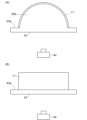
- FIG. 4 is a diagram for explaining the angular range of reflected waves reflected by the radio wave reflector according to the embodiment of the present invention
- FIG. 3B is a cross-sectional view along line BB in FIG. 3B, showing a schematic overall configuration of a radio wave reflector according to an embodiment of the present invention
- 3 shows a schematic configuration of the whole radio wave reflector shown in FIG. 2
- (A) is a plan view
- (B) is an enlarged view of part A of (A).
- (A) to (E) are plan views of conductors showing other examples of arrangement patterns of conductors.
- FIG. 10 is a plan view of conductors showing another example of an arrangement pattern of conductors;
- FIG. 10 is a plan view of conductors showing another example of an arrangement pattern of conductors;
- FIG. 10 is a plan view of a radio wave reflector showing another example of an arrangement pattern of conductors
- FIG. 5 is a cross-sectional view showing a schematic configuration of a radio wave reflector according to another embodiment
- FIG. 5 is a cross-sectional view showing a schematic configuration of a radio wave reflector according to another embodiment
- (A) is an explanatory diagram showing an example of application of the building material to a building
- (B) is a plan view showing an example of application of the building material to a room. It is a figure for demonstrating the evaluation method of reflection direction correctability. It is a figure for demonstrating the uneven
- the radio wave reflector 11 of this embodiment reflects radio waves output from the radio wave source 20, as shown in FIG.
- the reflected wave is received by the receiver 21 .
- the radio wave source 20 is a communication device or the like having a transmission antenna capable of transmitting radio waves.
- the receiver 21 is a device capable of receiving radio waves.
- the receiving unit 21 according to this embodiment is a communication device having a receiving antenna. Examples of communication devices include smartphones, mobile phones, tablet terminals, notebook PCs, portable game machines, repeaters, radios, and televisions.
- the radio wave reflector 11 includes a conductor 12 that reflects radio waves. With the radio wave reflector 11 flat, the incident angle of the incident wave is at least a predetermined angle of 15 degrees or more and 75 degrees or less, preferably 45 degrees, more preferably 15 degrees or more and 75 degrees or less. In all cases, radio waves with incident wave frequencies of 2 GHz to less than 6 GHz, 6 GHz to less than 20 GHz, 20 GHz to less than 60 GHz, 60 GHz to less than 100 GHz, 100 GHz to less than 150 GHz, or 150 GHz to 300 GHz are reflected by the radio wave reflector 11.
- the specular reflection intensity is ⁇ 30 dB or more and 0 dB or less with respect to the incident wave.
- the specular reflection intensity is ⁇ 30 dB or more and 0 dB or less with respect to the incident wave at a frequency of 28.5 GHz, and more preferably, the specular reflection intensity is ⁇ 30 dB or more with respect to the incident wave in the entire frequency band of 20 GHz or more and 60 GHz or less.
- the regular reflection intensity is -30 dB or more and 0 dB or less with respect to the incident wave in the entire frequency band of 2 GHz or more and 300 GHz or less.
- “Specular reflection intensity” is the intensity of reflected radio waves, and refers to the intensity of a reflected wave when an incident wave is specularly reflected.
- the term “flat” refers to a state in which there is no unevenness and is not curved, or a state in which the radius of curvature of any point on the surface is 1000 mm or more even when unevenness is present.
- the specular reflection intensity is preferably ⁇ 25 dB or more and 0 dB or less, more preferably ⁇ 22 dB or more and 0 dB or less, further preferably ⁇ 20 dB or more and 0 dB or less, and even more preferably ⁇ 15 dB or more and 0 dB or less with respect to the incident wave. Since the specular reflection intensity is ⁇ 30 dB or more with respect to the incident wave, the radio wave reflector 11 can reflect radio waves while maintaining a high reflection intensity, and the receiving section 21 has a practical intensity for use. Can receive radio waves.
- the specular reflection intensity and the reflection intensity are the distance between the reflection point 11a of the radio wave reflector 11 and the radio wave source 20 and the distance between the reflection point 11a of the radio wave reflector 11 and the receiving section 21. This is the value when the distance is 1 m.
- specular reflection means that when the radio wave emitted from the radio wave source 20 (transmitting antenna) is reflected by the radio wave reflector 11, the incident angle ⁇ 1 of the incident wave and the reflection of the reflected wave It means that the angle ⁇ 2 is equal.
- the reflection direction of the reflected wave when the radio wave is specularly reflected is also called the “specular reflection direction”.
- the incident angle ⁇ 1 is defined by the incident wave traveling in the incident direction (indicated by arrow A1 in FIG. 1) when the radio wave enters the radio wave reflector 11 and the normal line 22 of the reflecting surface of the radio wave reflector 11. is the angle.
- the angle of reflection ⁇ 2 is the angle formed between the reflected wave traveling in the reflection direction of the reflected wave (indicated by arrow A2 in FIG. 1) and the normal line 22 of the reflecting surface.
- the normal line 22 is a straight line perpendicular to the tangent line (or tangent plane) at the reflection point 11a.
- the intensity of the reflected wave is hereinafter also referred to as "reflection intensity”.
- the surface resistivity of the radio wave reflector 11 when the radio wave reflector 11 is flat is 0.003 ⁇ / ⁇ or more and 10 ⁇ / ⁇ or less. Although the details will be described later, the surface resistivity is measured as the surface resistivity of the conductive thin film layer 16 including the conductor 12 .
- the surface resistivity of the radio wave reflector 11 when the radio wave reflector 11 is flat refers to the surface resistivity of the radio wave reflector 11 when the radio wave reflector 11 is placed on a flat mounting surface.
- the term “flat” refers to a state in which there is no unevenness and is not curved, or a state in which the radius of curvature of any point on the surface is 1000 mm or more even when unevenness is present.
- Surface resistivity means surface resistance per square centimeter.
- the surface resistivity can be measured by the four-probe method in accordance with JISK6911 by contacting a measuring terminal to the surface of the conductive thin film layer 16, which will be described later. If the conductive thin film layer 16 is not exposed because it is protected by a resin sheet or the like, a non-contact resistance measuring device (manufactured by Napson Co., Ltd., trade name: EC-80P, or equivalent) is used. It can be measured by an eddy current method.
- the radio wave reflector 11 has a surface resistivity change rate R of -10% or more and 10% or less when curved.
- the rate of change R of the surface resistivity when curved is the ratio of the surface resistivity R1 of the wave reflector 11 when the wave reflector 11 is flattened to the surface resistivity R1 of the wave reflector 11 when the wave reflector 11 is a member having a curved surface with a curvature radius of 200 mm. It refers to the rate of change in the surface resistivity R2 in the state of being curved along the surface.
- the surface resistivity change rate R (%) (R2 ⁇ R1)/R1 ⁇ 100.
- the reflection intensity of radio waves changes according to the surface resistivity.
- the rate of change R of the surface resistivity of the radio wave reflector 11 when it is bent is -10% or more and 10% or less, even when the radio wave reflector 11 is curved, it is sufficiently similar to when it is flattened. It is possible to achieve a high reflection intensity of radio waves.
- the radio wave reflector 11 preferably has a bending elastic modulus of 0.05 GPa or more and 4 GPa or less.
- the flexural modulus is a value that indicates how much bending stress can be endured, and is defined in JIS K7171.
- the radio wave reflector 11 has flexibility, and the radio wave reflector 11 can be curved without breaking, and a curved surface with a radius of curvature of 200 mm or more can be obtained. can be pasted on.
- the flexural modulus is measured according to JIS K7171. Flexibility refers to the property of having flexibility under normal temperature and normal pressure, and being able to bend, bend, bend, or otherwise deform without being sheared or broken even when a force is applied.
- the radio wave reflector 11 preferably has a Young's modulus of 0.01 GPa or more and 80 GPa or less. Young's modulus refers to the elastic modulus when a solid is stretched by applying tension in one direction, and is also called the tensile elastic modulus, and is defined in JIS K7161-2014. By setting the Young's modulus within the above range, the radio wave reflector 11 is easily deformed, and the radio wave reflector 11 is curved without being broken, and is attached to a curved surface with a radius of curvature of 200 mm or more. be able to. Young's modulus is measured according to JIS K7127-1999.
- the radio wave reflector 11 has at least a degree of flexibility that allows it to be attached along a curved surface with a radius of curvature of 200 mm or more, preferably a degree that allows it to be attached along a curved surface with a radius of curvature of 100 mm or more. of flexibility.
- the radio wave reflector 11 may have plasticity.
- Plasticity refers to the property of being able to deform by applying external pressure, and retaining the deformed shape even when the force is removed when deformation exceeding the elastic limit is given by pressure. All of the synthetic resins forming the base layer 13, the adhesive layer 14, and the protective layer 15 may have plasticity, or at least one of the base layer 13, the adhesive layer 14, and the protective layer 15 may have plasticity. One may have plasticity.
- the radio wave reflector 11 has a difference between the yellow index after the heat and humidity resistance test and the yellow index before the heat and humidity resistance test, that is, the degree of yellowing is 3 or less.
- the yellow index is also called yellowness, and refers to the degree to which the hue deviates from colorless or white toward yellow.
- a yellow index is calculated
- the radio wave reflector 11 is removed from the constant temperature and humidity chamber. This is a test for confirming the properties and conditions of the radio wave reflector 11 after taking it out and allowing it to stand at room temperature for 4 hours.
- the incident wave is incident on the radio wave reflector 11 at a predetermined angle of 15 degrees or more and 75 degrees or less, preferably 45 degrees, more preferably 15 degrees or more and 75 degrees or less.
- an incident wave with a frequency of 2 GHz or more and 300 GHz or less is specularly reflected.
- the difference in intensity of reflected waves from the radio wave reflector 11 before and after the heat and humidity resistance test is within 3 dB in all frequency bands from 2 GHz to 300 GHz.
- the radio wave reflector 11 has a surface resistivity change rate r before and after the heat and humidity resistance test (also referred to as "surface resistivity change rate during the heat and humidity resistance test") of 20% or less.
- the change rate r of the surface resistivity during the heat and humidity resistance test refers to the rate at which the surface resistivity r2 after the heat and humidity resistance test changes with respect to the surface resistivity r1 before the heat and humidity resistance test.
- the reflection intensity of radio waves changes according to the surface resistivity. However, since the rate of change r of the surface resistivity of the radio wave reflector 11 during the heat and humidity resistance test is 20% or less, the reflection intensity of the radio wave reflector 11 does not decrease significantly even after the heat and humidity resistance test. The reflection intensity of radio waves can be realized.
- the pencil hardness of the protective layer 15 with a surface load of 500 g is preferably "F” or higher, more preferably “H” or higher. It is preferably “4H” or more.
- the "pencil hardness test” as used herein is a test based on JIS K 5600-5-4 (1999). "Surface load of 500 g" is included if the load applied to the surface during the pencil hardness test is 500 g ⁇ 10 g.
- the pencil hardness of the protective layer 15 with a surface load of 500 g may be F or higher.
- the reduction rate of the adhesive force of the protective layer 15 to the adherend layer is preferably 50% or less, more preferably 45% or less, and further Preferably it is 40% or less.
- "attached layer” means a layer that is in direct contact with the layer of interest.
- the adhered layer of the protective layer 15 is the adhesive layer 14 in this embodiment.
- the adhesive force is measured by a tensile adhesive strength test according to JIS K 6849 (1994).
- the radio wave reflector 11 is configured such that the receiving angular position of the reflected wave is -15 degrees or more and +15 degrees with respect to the regular reflection direction of the radio wave on a virtual plane including the incident direction of the incident wave and the reflection direction of the reflected wave. It is preferable that the kurtosis of the intensity distribution of the reflected wave at each receiving angular position is ⁇ 0.4 or less when the angular range ⁇ is varied as follows.
- the kurtosis is more preferably ⁇ 1.0 or less, still more preferably ⁇ 1.1 or less, and even more preferably ⁇ 1.2 or less. Although the lower limit of the kurtosis is not particularly limited, it is usually about -0.5.
- the virtual plane can also be said to be a plane including the reflection point 11a on the reflecting surface of the reflector, the radio wave source 20, and the reflected wave receiver 21. FIG. The kurtosis is obtained with the radio wave reflector 11 flattened.
- Kurtosis is a statistic that indicates how much a distribution deviates from a normal distribution, and indicates the degree of kurtosis and the spread of tails.
- the reception angular position i of the receiving unit 21 is set at a predetermined angle (for example, at a time of 5 degrees) from the specular reflection direction of the radio wave centering on the reflection point 11a, at ⁇ 15 degrees or more and +15 degrees or less with respect to the specular reflection direction of the radio wave.
- the reflection intensity x is measured by moving within the angle range ⁇ .
- the reception angular position i of the receiver 21 is positioned on an arc centered on the reflection point 11a. Reflection intensity value at each reception angular position i the average value of , and the standard deviation is s, the kurtosis is obtained from the following formula.
- kurtosis indicates that the intensity data at each angular position is distributed flatter than the normal distribution. The smaller is, the flatter the distribution.
- the difference in reflection intensity depending on the reception angular position becomes small within the angular range ⁇ of ⁇ 15 degrees with respect to the specular reflection direction of the radio wave.
- the radio wave reflector 11 may have visible light transmittance as a whole, that is, may be transparent. Although the details will be described later, the radio wave reflector 11 includes at least a base layer 13 and a conductive thin film layer 16 composed of a conductor 12, and preferably further includes an adhesive layer 14 and a protective layer 15. FIG.
- the base material layer 13, the adhesive layer 14, and the protective layer 15 may each be made of a resin that transmits visible light.
- transparent means that the other side of the radio wave reflector 11 can be viewed from one side, and includes semi-transparency, but is not limited to complete transparency with a total light transmittance of 100%.
- the radio wave reflector 11 may be colored.
- the radio wave reflector 11 has a total light transmittance of 65% or more, preferably 80% or more, more preferably 85% or more, and still more preferably 90% or more under a D65 standard light source.
- the total light transmittance refers to the ratio of the total transmitted light flux to the parallel incident light flux of the test piece, and is measured according to JISK 7375:2008.
- the radio wave reflector 11 preferably has a square overall shape in plan view and a side length L10 of 20 cm or more and 400 cm or less. Radio waves with a frequency of 2 GHz or more and 300 GHz or less are attenuated by distance, but in order to reflect with sufficient intensity at all points within a practical distance from the radio wave source 20, the length of one side L10 is set to 20 cm or more. is preferred. Although the upper limit of the length L10 of one side is not particularly limited, it is preferably 400 cm or less from the viewpoint of manufacturing.
- the overall shape of the radio wave reflector 11 is not limited to a square, but may be a rectangle, or may be a polygon such as a triangle, pentagon, or hexagon. be done.
- the shortest distance between a certain vertex and the opposite side or the shortest distance between a certain side and the opposite side may be set to 20 cm or more and 400 cm or less.
- the overall shape of the radio wave reflector 11 when the overall shape of the radio wave reflector 11 is circular, the diameter is set to 20 cm or more and 400 cm or less.
- the overall shape of the radio wave reflector 11 is elliptical, the minor axis is set to 20 cm or more and 400 cm or less.
- the overall shape of the radio wave reflector 11 is fan-shaped, the length of the arc or the shorter radius is set to 20 cm or more and 400 cm or less.
- the overall shape of the radio wave reflector 11 may be a three-dimensional shape such as a cylindrical shape or a conical shape.
- the overall shape of the radio wave reflector 11 has a shape and size that can reflect radio waves with a reflection intensity of -30 dB or more with respect to the incident wave. is appropriately selected according to the aspect of
- the radio wave reflector 11 preferably has a thickness L11 of 0.01 mm or more and 0.5 mm or less.
- the thicknesses of the substrate layer 13, the conductive thin film layer 16, the adhesive layer 14, and the protective layer 15 are set so that the thickness L11 of the radio wave reflector 11 is 0.5 mm or less.
- the thickness L11 of the radio wave reflector 11 is such that the radio wave reflector 11 can be flexible, and the thickness L11 of the conductive thin film layer 16 is sufficient when the radio wave reflector 11 is bent by applying an external force to the radio wave reflector 11.
- the thickness is set so that the force is not concentrated on the conductor 12 and the force can be distributed to the base layer 13 , the adhesive layer 14 and the protective layer 15 .
- the radio wave reflector 11 has at least a degree of flexibility that allows it to be attached along a curved surface with a radius of curvature of 200 mm or more, preferably a degree that allows it to be attached along a curved surface with a radius of curvature of 100 mm or more. of flexibility.
- the thickness L11 of the radio wave reflector 11 is the sum of the thickness L3 of the conductive thin film layer 16 and the thickness L8 of the base layer 13, or the thickness L3 of the conductive thin film layer 16, the thickness L8 of the base layer 13 and the adhesive layer 14. It is the sum of the thickness L4 and the thickness L5 of the protective layer 15 .
- the thickness L3 of the conductive thin film layer 16 is much thinner than the respective thicknesses L8, L4, and L5 of the base layer 13, the adhesive layer 14, and the protective layer 15, when calculating the thickness L11 of the radio wave reflector 11, Alternatively, the thickness L3 of the conductive thin film layer 16 may be ignored.
- the thickness L11 of the radio wave reflector 11, the thickness L3 of the conductive thin film layer 16, the thickness L8 of the base layer 13, the thickness L4 of the adhesive layer 14, and the thickness L5 of the protective layer 15 are measured at a plurality of arbitrary points. , is obtained by calculating the average value of the obtained measured values.
- a reflectance spectroscopic film thickness measurement for example, F3-CS-NIR manufactured by Filmetrics Co., Ltd. is used as a measuring instrument. .
- the radio wave reflector 11 includes a conductive thin film layer 16 containing a conductor 12, a base material layer 13 laminated on the conductive thin film layer 16 and containing a base material, and a protective layer containing a protective material for protecting the conductive thin film layer 16. 15 and an adhesive layer 14 containing an adhesive for bonding the conductive thin film layer 16 and the protective layer 15 together. Further, the radio wave reflector 11 may include a conductive thin film layer 16 containing the conductor 12 and a resin that keeps the conductor 12 in a sheet shape.
- the radio wave reflector 11 has a conductive thin film layer 16 laminated on a substrate layer 13, and an adhesive layer 14 and a protective layer 15 laminated thereon in this order.
- the vertical direction is defined based on FIG. 2, and the vertical and horizontal directions are defined based on FIG. It does not stipulate the vertical and horizontal directions during use such as attachment to objects. 1 to 11 are not shown to scale. Also, in FIG. 3A, the adhesive layer 14 and the protective layer 15 are partially omitted from the radio wave reflector 11 .
- the base material layer 13 has a square outer shape in plan view. However, it is not limited to this, and may be rectangular, circular, elliptical, fan-shaped, polygonal, three-dimensional, or the like in accordance with the overall shape of the radio wave reflector 11 .
- a sheet made of a synthetic resin is used as the substrate which is the substrate layer 13 .
- Examples of synthetic resins include PET (polyethylene terephthalate), polyethylene, polypropylene, polyvinyl chloride, polystyrene, polymethyl methacrylate, polyester, polyformaldehyde, polyamide, polyphenylene ether, vinylidene chloride, polyvinyl acetate, polyvinyl acetal, and AS resin. , ABS resin, acrylic resin, fluorine resin, nylon resin, polyacetal resin, polycarbonate resin, polyamide resin, and polyurethane resin.
- the thickness L8 (length in the vertical direction in FIG. 2) of the base material layer 13 is set to 0.13 mm in this embodiment, but is not limited to this. is appropriately set according to the aspect of
- the base material layer 13 may contain an arbitrary material such as a synthetic resin or an arbitrary member.
- one or more linear conductors 12 are preferably formed as a thin film on the upper surface of the base layer 13 .
- the conductor 12 is preferably made of silver (Ag), for example.
- the conductor 12 may be made of a metal, metal compound, or alloy having free electrons, and is not limited to silver.
- gold Au
- copper Cu
- platinum Pt
- zinc Zn
- Iron Fe
- Tin Tin
- Lead Pb
- Aluminum Al
- Cobalt Co
- Indium In
- Nickel Ni
- Chromium Cr
- Titanium Ti
- Ultimone Sb
- bismuth Bi
- thallium Tl
- germanium Ge
- cadmium Cd
- silicon Si
- W tungsten
- Mo molybdenum
- ITO indium tin oxide
- alloys such as nickel, chromium and an alloy containing molybdenum
- the conductive thin film layer 16 may contain an arbitrary material such as synthetic resin or an arbitrary member.
- one or a plurality of linear conductors 12 are arranged to surround a region 12a where there are no conductors 12 . That is, conductors 12 and areas 12a without conductors 12 are periodically arranged at predetermined intervals. The conductors 12 and the regions 12a without the conductors 12 gather to form a thin film. The distance between adjacent regions 12a without conductors 12 may be equal to the line width L6 of the conductors 12, or may be longer than the line width L6.
- linear means that the length in the longitudinal direction is 3000 times or more the length in the direction orthogonal to the longitudinal direction. In the example shown in FIG.
- the conductors 12 are arranged at regular intervals along the vertical and horizontal directions, and a region 12a surrounded by the conductors 12 and having no conductors 12 is square. That is, the areas 12a without the conductors 12 are arranged at intervals of the line width L6 of the conductors 12.
- Conductors 12A and 12B are electrically connected at intersections where conductors 12 (12A) extending in the horizontal direction and conductors 12 (12B) extending in the vertical direction overlap.
- a line width L6 of the conductor 12 is preferably set to 0.05 ⁇ m or more and 15 ⁇ m or less.
- the distance L7 (the length of one side of the square area 12a without the conductors 12) between the conductors 12 adjacent to each other along the vertical or horizontal direction is greater than the wavelength of visible light and is reflected by the radio wave reflector 11.
- the wavelength is set to be smaller than the wavelength of the radio wave to be transmitted, and in this example, it is set to 2 ⁇ m or more and 10 cm or less. It is more preferably 20 ⁇ m or more and 1 cm or less, still more preferably 25 ⁇ m or more and 1 mm or less. More preferably, it is 30 ⁇ m or more and 250 ⁇ m or less.
- the thickness (film thickness) L3 of the conductor 12 is preferably a thickness that allows visible light transmission.
- the thickness L3 of the conductor 12 is preferably 0.05 ⁇ m or more and 10 ⁇ m or less.
- the thickness L3 is preferably 5 nm or more from the viewpoint of ensuring appropriate radio wave intensity.
- the surface roughness Sa of the conductive thin film layer 16 is not particularly limited, it is preferably 1 ⁇ m or more and 7 ⁇ m or less, more preferably 1.03 ⁇ m or more and 6.72 ⁇ m or less. When the surface roughness Sa is within this range, it becomes easier to diffusely reflect radio waves.
- the surface roughness Sa is determined by the arithmetic mean height of ISO 25178 and measured according to ISO 25178. Using a laser microscope (product name VK-X1000/1050, manufactured by Keyence Corporation, or equivalent), the surface roughness is measured at multiple locations on the surface of the conductive thin film layer 16, and the average value of the obtained measurement values can be calculated to obtain the surface roughness Sa of the conductive thin film layer 16 . In some cases, the conductor 12 and the base layer 13 are to be measured. In this embodiment, a plurality of conductors 12 are provided, and the surface roughness of each conductor 12 is measured at a plurality of locations, and the average value of the measured values is taken as the surface roughness Sa of the conductive thin film layer 16. do.
- the conductive thin film layer 16 preferably has a coverage of 1% or more and 50% or less, more preferably 1% or more and 10% or less.
- the coverage rate refers to the ratio of the area occupied by the conductor 12 per unit area in plan view. In the embodiments shown in FIGS. refers to the ratio of the area in plan view.
- the coverage can also be said to be the area of the base layer 13 covered with the conductor 12 with respect to the area of the base layer 13 in plan view. The coverage is measured using a scanning electron microscope (SEM), a transmission electron microscope (TEM), an optical microscope, or the like.
- the region 12a without the conductors 12 has a square shape.
- the distance between the conductors 12B extending in the direction may be different, and the shape of the region 12a without the conductors 12 may be rectangular.
- the conductors 12 may be arranged in the arrangement patterns shown in FIGS.
- FIG. 4A a plurality of conductors 12A extend in the horizontal direction and are arranged at predetermined intervals in the vertical direction.
- the bodies 12B are arranged in a staggered manner.
- the zigzag pattern means that a plurality of conductors 12B extending in the vertical direction are arranged in the horizontal direction at predetermined intervals, and the plurality of conductors 12B forming one row are adjacent to each other in the vertical direction of the row. It is positioned between a plurality of conductors 12B forming a row, and refers to a state in which the conductors 12B in alternate rows are arranged in a straight line.
- the conductor 12A extends in the lateral direction
- the conductors 12B and 12C extend in a symmetrical oblique direction with respect to the lateral direction
- the conductors 12B and 12C are conductive to each other.
- Cross on body 12A is arranged in the horizontal direction at predetermined intervals, and the plurality of conductors 12B forming one row are adjacent to each other in the vertical direction of the row. It is positioned between a plurality of conductors 12B forming a row, and refers to a state in which the conductor
- the shape of the region 12a without the conductor 12 is an equilateral triangle.
- the shape of the region 12a without the conductor 12 may be an isosceles triangle or a triangle with three sides of different lengths instead of an equilateral triangle.
- regular hexagonal regions 12a without conductors 12 surrounded by linear conductors 12 are periodically arranged, and in FIG. Enclosed regular pentagonal regions 12a without conductors 12 are periodically arranged.
- FIG. 4E circular regions 12a surrounded by linear conductors 12 and having no conductors 12 are arranged periodically. 4A to 4E show only the conductor 12.
- Examples of the method for manufacturing the conductive thin film layer 16 having the arrangement pattern shown in FIGS. 3(B) and 4 are as follows. After forming a conductive film, a pattern is formed by etching, and a patterned conductive thin film is taken out. and a method of taking out a conductive thin film body having a pattern after filling the pattern portion with a conductor.
- the manufacturing method is not limited to the above, and examples of methods for forming the conductive thin film layer 16 include a method of adhering a metal thin film and a method of vapor-depositing metal.
- FIG. 5 Another embodiment of the conductive thin film layer 16 is shown in FIG.
- a plurality of conductors 12 are periodically arranged in a sheet shape (thin film shape) on the upper surface of the base material layer 13 .
- a circular conductor 12 is used in plan view.
- the diameter L1 and the shortest distance (interval) L2 between the adjacent conductors 12 are set according to the frequency band of the reflected radio waves. In the present embodiment, it is set so as to reflect radio waves of 20 GHz or more and 300 GHz or less, which is the frequency band for the fifth generation mobile communication system (5G).
- 5G fifth generation mobile communication system
- the diameter L1 and the interval L2 may be set so that the conductor 12 reflects radio waves with a frequency of 2 GHz or more and 300 GHz or less.
- the diameter L1 of each conductor 12 may be 0.7 mm or more and 800 mm or less, and the interval L2 may be 1 ⁇ m or more and 1000 ⁇ m or less.
- the number of conductors 12 is appropriately set according to the size (area) of the base material layer 13 .
- a sheet shape means a shape in which the length in the longitudinal direction is approximately the same as or less than 3000 times the length in the direction orthogonal to the longitudinal direction.
- the shape of the conductor 12 is not limited to circular, and may be any shape.
- the sides of one conductor 12 and the sides of adjacent conductors 12 are parallel, and can be arranged periodically so that the distances between one conductor 12 and all adjacent conductors 12 are equal.
- it may be square, rectangular, triangular, hexagonal, or the like.
- the length of the shortest side of the conductor 12, the shortest distance between a vertex and the opposite side of the conductor 12, or the shortest distance between a certain side and the opposite side is 0.005 ⁇ m or more and 100 mm or less. may be set to More preferably, it may be set to 0.1 ⁇ m or more and 1000 ⁇ m or less. Since other configurations and actions are the same as those of the embodiment shown in FIGS. 2 and 3, the same reference numerals are assigned to the corresponding configurations, and detailed description thereof will be omitted.
- the conductive thin film layer 16 may have, for example, a metamaterial structure.
- the metamaterial structure is obtained by periodically arranging sheet-shaped conductors 12, which are dielectrics. Reflects radio waves belonging to The shape of each conductor 12 is not limited and may be the shape described above. For example, as shown in FIG. 6, each conductor 12 may be square.
- the length L12 of one side and the interval L13 between the adjacent conductors 12 may be set so that the conductors 12 reflect radio waves with a frequency of 2 GHz or more and 300 GHz or less.
- the length L12 of one side of the conductor 12 may be 0.7 mm or more and 800 mm or less, and the interval L13 may be 1 ⁇ m or more and 1000 ⁇ m or less.
- the thickness L3 of the conductor 12 is preferably 350 nm (0.35 ⁇ m) or less, more preferably 100 nm or less, and even more preferably 50 nm or less.
- the number of conductors 12 is appropriately set according to the size (area) of the base material layer 13 . In one example, the conductors 12 may be formed on the base layer 13 so as to match the size of the base layer 13 , two vertically and two horizontally, a total of four conductors 12 .
- the conductive thin film layer 16 is not limited to a metamaterial structure, and may be any one of a metal nanowire laminated film, multi-layered graphene, and partially exfoliated graphite. In addition to the conductor, the conductive thin film layer 16 may contain an arbitrary material such as synthetic resin or an arbitrary member.
- the adhesive layer 14 adheres the protective layer 15 onto the base material layer 13 and the conductive thin film layer 16, and is made of an adhesive.
- the adhesive layer 14 has a size corresponding to that of the base material layer 13 in plan view.
- a synthetic resin or rubber adhesive sheet is used as the adhesive that is the adhesive layer 14. Examples of synthetic resins include acrylic resins, silicon resins, polyvinyl alcohol resins, and the like.
- a thickness L4 of the adhesive layer 14 is preferably set to 5 ⁇ m or more and 500 ⁇ m or less.
- the adhesive layer 14 may contain any substance such as synthetic resin or any other member.
- the adhesive layer 14 is preferably made of a synthetic resin material with a dielectric loss tangent (tan ⁇ ) of 0.018 or less.
- a lower dielectric loss tangent is more preferable, but it is usually 0.0001 or more.
- the dielectric loss tangent represents the degree of electrical energy loss within a dielectric, and the greater the dielectric loss tangent of a material, the greater the electrical energy loss.
- the synthetic resin material of the adhesive layer 14 has a dielectric constant that changes according to the frequency of the electric field.
- the dielectric constant is the ratio of the dielectric constant of a medium (synthetic resin material in this embodiment) to the dielectric constant of a vacuum.
- the dielectric constant varies between 1.5 and 7. More preferably, it changes between 1.8 and 6.5.
- Inductive loss tangent and relative permittivity are measured using a known method (e.g., cavity resonator method, coaxial resonator method) using a measuring device (e.g., Toyo Technica, model number TTPX table-top cryogenic prober, material impedance analyzer MIA-5M). measured by
- the synthetic resin material constituting the base layer 13 and the protective layer 15 may have a dielectric loss tangent of 0.018 or less, and the dielectric constant changes according to the electric field. can be anything.
- the protective layer 15 has a size corresponding to that of the base material layer 13 in plan view, protects the conductor 12, and is made of a protective material.
- a synthetic resin sheet (film) is used as a protective material that is the protective layer 15 .
- synthetic resins include PET (polyethylene terephthalate), COP (cycloolefin polymer), polyethylene, polypropylene, polyvinyl chloride, polystyrene, polymethyl methacrylate, polyester, polyformaldehyde, polyamide, polyphenylene ether, vinylidene chloride, and polyvinyl acetate.
- the thickness L5 of the protective layer 15 is preferably set to 0.02 mm or more and 0.30 mm or less.
- the protective layer 15 may contain an arbitrary substance such as synthetic resin or an arbitrary member.
- anti-glare treatment or anti-reflection treatment may be applied to at least one of the upper surface (outer surface) and lower surface (surface in contact with the adhesive layer 14) in FIG. 2 of a synthetic resin film.
- Anti-glare treatment involves forming an uneven shape on at least one surface of the protective layer 15 to scatter light and reduce reflection of a light source such as illumination on the protective layer 15 . This is a process that suppresses congestion.
- a method of applying anti-glare treatment for example, a method of applying a binder resin in which fine particles are dispersed is applied to the surface of the film. Also, known methods such as sandblasting and chemical etching may be used.
- Antireflection treatment (also referred to as “AR treatment”) is to form an antireflection film on at least one surface of the film, and reflect light reflected from the surface of the antireflection film and from the interface between the antireflection film and the film. This is a process of attenuating the reflected light by interference to suppress reflection of a light source such as illumination.
- the anti-reflection film may be a single layer, or may be one in which thin films having different refractive indices are alternately laminated, and known anti-reflection films are used.
- the protective layer 15 may be a synthetic resin film with anti-glare treatment or anti-reflection treatment attached to one side or both sides of the film.
- the protective layer 15 preferably has a moisture permeability at a temperature of 40° C. and a humidity of 90% rh (relative humidity) of 20 g/m 2 ⁇ 24 h or less, more preferably 16 g/m 2 ⁇ 24 h or less, More preferably, it is 12 g/m 2 ⁇ 24h or less, and still more preferably 10 g/m 2 ⁇ 24h or less.
- the moisture permeability of the protective layer 15 at a temperature of 40° C. and a humidity of 90% rh (relative humidity) is 20 g/m 2 ⁇ 24 h or less
- the conductive thin film layer 16 is less likely to corrode, and the surface resistivity of the conductive thin film layer 16 is improved. has the advantage of being less likely to rise.
- the "water vapor permeability" referred to in this specification is measured by a test method based on JIS Z 0208 (1976).
- FIG. 7 shows another embodiment of the invention.
- the radio wave reflector 11 shown in FIG. 7 is formed by vertically laminating two layers of base layers 13A and 13B in which the conductors 12A and 12B are made of resin.
- the conductors 12A formed on the base layer 13A and the conductors 12B formed on the base layer 13B are aligned and laminated so as to overlap each other when viewed from above.
- the arrangement patterns of the conductive thin film layers 16A and 16B in FIG. 7 may not overlap in plan view, and the conductive thin film layers 16A and 16B may be formed in different arrangement patterns.
- the lower surface of the base material layer 13B is attached on the conductor 12A with an adhesive layer 14A, and the protective layer 15 is attached on the conductor 12B with an adhesive layer 14B.
- the Young's modulus is preferably 0.01 GPa or more and 80 GPa or less
- the thickness of the radio wave reflector is preferably 0.01 mm or more and 0.5 mm or less.
- the radio wave reflector 11 has a total light transmittance of 70%.
- the radio wave incident on the radio wave reflector 11 is reflected by the conductor 12B in the first layer, but part of it passes through the conductor 12B without being reflected by the conductor 12B.
- the radio waves passing through the conductor 12B are reflected by the conductor 12A in the second layer. In this way, by stacking a plurality of conductors 12 in the vertical direction, radio waves passing through the conductor 12B in the upper layer can be reflected by the conductor 12A in the lower layer. can be kept larger than in the case of only one layer.
- the kurtosis of the reflection intensity distribution in the angle range ⁇ of ⁇ 15 degrees with respect to the specular reflection direction of the radio wave can be further reduced, and the difference in reflection intensity depending on the angular position within the angle range ⁇ becomes smaller. Furthermore, since the two adhesive layers 14A and 14B are used, the value of the dielectric loss tangent becomes even smaller than in the embodiment shown in FIG. 2, and the reflection intensity can be kept even higher. Since other configurations and actions are the same as those of the embodiment shown in FIGS. 2 and 3, the same reference numerals are assigned to the corresponding configurations, and detailed description thereof will be omitted.
- the conductors 12 formed on the base material layer 13 are laminated in two layers, but may be laminated in three or more layers. As the number of laminated conductors 12 increases, the reflection intensity increases, but the overall thickness of the radio wave reflector 11 increases, resulting in a decrease in flexibility and a decrease in visible light transmittance. Therefore, the number of laminations is appropriately set according to the intended use, such as increasing the number of laminations when the radio wave reflector 11 is provided in a place where flexibility or transparency is not particularly required.
- FIG. 8 Another embodiment of the radio wave reflector 11 is shown in FIG.
- a conductive thin film layer 16 composed of a plurality of linear conductors 12 similar to those in the embodiment shown in FIGS. 2 and 3 and a substrate layer 13 are provided.
- the bending elastic modulus is preferably 0.05 GPa or more and 4 GPa or less
- the Young's modulus is preferably 0.01 GPa or more and 80 GPa or less
- the thickness of the radio wave reflector is 0.01 mm or more and 0.5 mm.
- the radio wave reflector 11 has a total light transmittance of 70%. Since other configurations and actions are the same as those of the embodiment shown in FIGS. 2 and 3, the same reference numerals are assigned to the corresponding configurations, and detailed description thereof will be omitted.
- the conductive thin film layer 16 is composed of a plurality of linear conductors 12, but the conductive thin film layer 16 is not limited to this embodiment.
- the sheet-shaped conductor 12 may be formed in a square shape on substantially the entire upper surface of the base material layer 13 .
- the coverage is defined as the ratio of the area occupied by the conductor 12 per unit area in the portion where the conductive thin film layer 16 is provided on the base layer 13, and the coverage is 100%.
- the size of the conductor 12 may be one size smaller than the size of the base layer 13 in plan view, and the conductor 12 may not be formed in a region near the side edge of the base layer 13 .
- the conductive thin film layer 16 of the embodiment shown in FIG. 8 is formed by periodically arranging a plurality of sheet-like conductors 12 in the same manner as the conductive thin film layer 16 of the embodiment shown in FIG. may In this case, the plurality of conductors 12 are arranged at predetermined intervals over substantially the entire upper surface of the base material layer 13 . Also, the shape of the conductor 12 may be square, circular, rectangular, triangular, polygonal, or the like.
- the conductive thin film layer 16 may have a metamaterial structure, and may be any one of a metal nanowire laminated film, multi-layered graphene, and partially exfoliated graphite.
- any of the radio wave reflectors 11 described above may be included in the building material 30 and used.
- the building material 30 is, for example, as shown in FIG. 9(A), wall surfaces, ceiling surfaces, floor surfaces of rooms and corridors, wallpaper for partitions, decorative materials 30A such as posters, and decorative materials such as transparent stickers for light covers.
- 30B can be installed in a building.
- the radio wave reflector 11 may be formed as a member made of a non-conductive material such as resin or held inside a building material.
- the wall surface 31 itself, which is the building material 30 , or the lamp cover 32 itself may be composed of the radio wave reflector 11 .
- the building material 30 is not limited to indoor walls and light covers, and may be, for example, partitions, pillars, lintels, outer walls of buildings, windows, and the like.
- FIG. 9B is a plan view of the interior of the room, and the building material 30, which is the radio wave reflector 11, is formed as a corner pillar 30C having a curved surface at the corner of the room. The radio wave entering from the window 33 is reflected by the corner post 30C and reaches a wider range of the indoor space S.
- 9(A) and 9(B) show an application example of the building material 30, and do not show the actual range of radio wave reflection.
- Examples 1 to 9 were produced as the radio wave reflector 11, and evaluation tests were conducted on the reflection direction correctability and irregularity followability for Examples 1 to 9 and Comparative Examples 1 to 4.
- the radio wave reflector 11 of the present invention is not limited to Examples 1-9.
- Example 1 shows the details of Examples 1 to 9 and Comparative Examples 1 to 4 and the results of evaluation tests.
- Examples 1 to 9 and Comparative Examples 1 to 4 have any one of "configuration A” to "configuration D” and "metal plate” as the configuration of the radio wave reflector.
- Configuration A is a configuration in which a substrate layer 13, a conductive thin film layer 16 (conductor 12), an adhesive layer 14, and a protective layer 15 are laminated in order, as in the embodiment shown in FIGS.
- a synthetic resin material sheet made of PET as the substrate layer 13 and the protective layer 15 (manufactured by Toray Industries, Lumirror 50T60, product number #125-U34 when the thickness of the substrate layer 13 and protective layer 15 is 0.13 mm, thickness 0.13 mm). In the case of 19 mm, product number #188-U34) was used.
- Configuration B is a configuration in which a conductive thin film layer 16 (conductor 12) is laminated on a base material layer 13, as in the embodiment shown in FIG.
- a synthetic resin material sheet TOMBP No. 9000 manufactured by NICHIAS Corporation
- PTFE fluororesin
- Configuration C is a configuration in which a conductive thin film layer 16 (conductor 12) is laminated on a substrate layer 13, as in the embodiment shown in FIG. G-Leaf manufactured by Electric Glass Co., Ltd.) was used.
- Configuration D is a configuration in which a base layer 13, a conductive thin film layer 16 (conductor 12), an adhesive layer 14, and a protective layer 15 are laminated in order, as in the embodiment shown in FIGS.
- the substrate layer 13 is different from that of configuration A.
- a synthetic resin material sheet Midfil NS manufactured by Kurashiki Boseki Co., Ltd.
- PEEK polyetheretherketone
- Metal plate is a structure consisting of a single metal plate.
- connection type means that, as shown in FIGS. 3B and 4, one or a plurality of linear conductors 12 are arranged surrounding a region 12a where there are no conductors 12, that is, , conductors 12 and areas 12a without conductors 12 are periodically arranged at predetermined intervals.
- isolated type means that sheet-shaped conductors 12 are periodically arranged as shown in FIG. 5 or 6 .
- the shape of the arrangement pattern of the conductors 12 is shown as “zigzag”, “lattice”, and “circular”. “Staggered” means that the arrangement pattern of the conductors 12 is “connected”, and the conductors 12 are staggered as shown in FIG. 4(A).
- the “lattice pattern” is a case where the arrangement pattern of the conductors 12 is “connected type”, and the conductors 12 are arranged at equal intervals along the vertical and horizontal directions as shown in FIG. 3B.
- the shape is "Circular” means that the arrangement pattern of the conductors 12 is “isolated”, and the shape of each conductor 12 is circular as shown in FIG.
- the adhesive used for the adhesive layer 14 is shown as "rubber-based” and "acrylic-based".
- rubber-based is meant a rubber-based adhesive.
- the rubber-based adhesive was obtained by the following method. A reaction vessel equipped with a cooling tube, a nitrogen inlet tube, a thermometer, a dropping funnel and a stirring device was charged with a rubber-based polymer (styrene-(ethylene-propylene)-styrene type block copolymer 50% by mass and styrene-(ethylene-propylene ) type block copolymer 50% by mass, styrene content 15%, weight average molecular weight 130,000) 100 parts by weight, synthetic resin (manufactured by Mitsui Chemicals, FMR-0150) 40 parts by weight, softener (JX Nikko Nisseki Energy Co., Ltd., LV-100) 20 parts by weight, antioxidant (ADEKA Co., Ltd., Adekastab AO-330) 0.5 parts by weight and to
- Acrylic refers to acrylic adhesives.
- the acrylic adhesive was obtained by the following method. Monofunctional long-chain urethane acrylate (PEM-X264 manufactured by AGC, molecular weight 10000) 40 parts by weight, and acrylic monomer 60 parts by weight (2-ethylhexyl acrylate (2EHA) 35 parts by weight, cyclohexyl acrylate (CHA) 10 parts by weight, 2-hydroxy 10 parts by mass of ethyl acrylate (2HEA) and 5 parts by mass of dimethylacrylamide (DMAA)) were mixed and stirred.
- PEM-X264 Monofunctional long-chain urethane acrylate
- EHA 2-ethylhexyl acrylate
- CHA cyclohexyl acrylate
- 2-HEA 2-hydroxy 10 parts by mass of ethyl acrylate
- DMAA dimethylacrylamide
- a crosslinking agent (1.6 hexanediol diacrylate (A-HD -N, manufactured by Shin Nakamura Chemical Co., Ltd.)) and a photopolymerization initiator (Omnirad 651 (manufactured by IGM Japan LLC)) were added, stirred, and vacuum degassed. An acrylic adhesive was thus obtained.
- a crosslinking agent 1.6 hexanediol diacrylate (A-HD -N, manufactured by Shin Nakamura Chemical Co., Ltd.)
- a photopolymerization initiator (Omnirad 651 (manufactured by IGM Japan LLC)
- the adhesive layer 14 has a dielectric loss tangent value of 0.002, which is 0.018 or less.
- the radio wave reflector 11 produced as Example 1 has the configuration of "Configuration A”.
- the radio wave reflector 11 has a square planar shape, a side length L10 of 100 cm, and a thickness L11 of 0.4 mm.
- the radio wave reflection intensity in a flat state ("specular reflection intensity at 28.5 GHz in a flat state” in Table 1) is -24 dB, the Young's modulus is 0.08 GPa, the bending elastic modulus is 2.2 GPa, and the surface resistivity is 1.7 ⁇ / ⁇ , and the rate of change R of the surface resistivity during bending is 4.3%.
- the radio wave reflector 11 has a total light transmittance of 89%.
- the thickness L8 of the base material layer 13 is 0.13 mm.
- the arrangement pattern of the conductors 12 of the conductive thin film layer 16 is a connected type, and the arrangement pattern is staggered.
- the line width L6 of the conductor 12 is 400 nm, the thickness L3 of the conductor 12 is 0.4 ⁇ m, and the interval L7 between the adjacent conductors 12 is 100 ⁇ m (tolerance ⁇ 10 ⁇ m, the same applies hereinafter).
- the conductor 12 is a metal thin film made of silver (Ag).
- the conductive thin film layer 16 has a surface roughness Sa of 1.1 ⁇ m and a coverage of 0.80%.
- the adhesive layer 14 is made of rubber, the thickness L4 of the adhesive layer 14 is 0.04 mm, and the thickness L5 of the protective layer 15 is 0.13 mm.
- the conductor 12 is formed on the base layer 13 .
- a core layer of 0.01 ⁇ m or more and 3 ⁇ m or less is formed on one surface of a copper foil having a thickness of 5 ⁇ m or more and 200 ⁇ m or less, which has sufficient strength as a metal layer, by a method such as electrolytic or electroless plating.
- a conductive thin film layer 16 having a predetermined arrangement pattern is formed on the surface of the core layer by a method such as electrolytic or electroless plating.
- the entire conductive thin film layer 16 is covered with the base material layer 13 .
- An adhesive is applied to the base layer 13 in advance.
- the copper foil and core layer are removed by etching. Thereby, the conductor 12 is formed on the base material layer 13 .
- the protective layer 15 is attached to the side of the conductor 12 opposite to the base layer 13 by the adhesive layer 14 .
- the protective layer 15 is adhered onto the conductor 12 of the substrate layer 13 so as to prevent air bubbles from entering.
- the radio wave reflector 11 is manufactured.
- the radio wave reflector 11 produced as Example 2 has the configuration of "Configuration B" and does not include the adhesive layer 14 and the protective layer 15.
- the thickness L11 of the radio wave reflector 11 is 0.08 mm.
- the radio wave reflection intensity in the flat state is -23 dB
- the Young's modulus is 0.5 GPa
- the flexural modulus is 0.6 GPa
- the surface resistivity is 1.4 ⁇ / ⁇
- the change rate R of the surface resistivity when bending is 2.0. 8%.
- the radio wave reflector 11 has a total light transmittance of 0.1%.
- the thickness L8 of the base material layer 13 is 0.08 mm.
- the arrangement pattern of the conductors 12 of the conductive thin film layer 16, the shape of the arrangement pattern, the line width L6, the thickness L3, the interval L7 between the adjacent conductors 12, the materials of the conductors, and other configurations are the same as in the first embodiment. be.
- the radio wave reflector 11 of Example 2 is manufactured in the same manner as in Example 1, but the adhesive layer 14 and protective layer 15 are not provided.
- the radio wave reflector 11 produced as Example 3 has the same "configuration A" as Example 1.
- the thickness L11 of the radio wave reflector 11 is 0.5 mm.
- the radio wave reflection intensity in the flat state is -25 dB
- the Young's modulus is 0.08 GPa
- the bending elastic modulus is 2.2 GPa
- the surface resistivity is 1.5 ⁇ / ⁇
- the surface resistivity change rate R during bending is 9.0. 8%.
- the radio wave reflector 11 has a total light transmittance of 87%.
- the thickness L8 of the base material layer 13 is 0.19 mm.
- the adhesive layer 14 is made of rubber, the thickness L4 of the adhesive layer 14 is 0.12 mm, and the thickness L5 of the protective layer 15 is 0.19 mm.
- the arrangement pattern of the conductors 12 of the conductive thin film layer 16 the shape of the arrangement pattern, the line width L6, the thickness L3, the interval L7 between the adjacent conductors 12, the materials of the conductors, and other configurations are the same as in the first embodiment. be.
- the radio wave reflector 11 produced as Example 4 has the configuration of "Configuration C" and does not include the adhesive layer 14 and the protective layer 15.
- the thickness L11 of the radio wave reflector 11 is 0.05 mm.
- the radio wave reflection intensity in the flat state is -26 dB
- the Young's modulus is 70 GPa
- the bending elastic modulus is 0.05 GPa
- the surface resistivity is 3.8 ⁇ / ⁇
- the surface resistivity change rate R during bending is 3.9%. is.
- the radio wave reflector 11 has a total light transmittance of 90%.
- the thickness L8 of the base material layer 13 is 0.05 mm.
- the arrangement pattern of the conductors 12 of the conductive thin film layer 16 is a connected type, and the arrangement pattern has a lattice shape.
- the radio wave reflector 11 of Example 4 is manufactured in the same manner as in Example 1, but the adhesive layer 14 and protective layer 15 are not provided.
- the radio wave reflector 11 produced as Example 5 has the configuration of "configuration D".
- the thickness L11 of the radio wave reflector 11 is 0.5 mm.
- the radio wave reflection intensity in the flat state is -25 dB
- the Young's modulus is 0.1 GPa
- the bending elastic modulus is 3.7 GPa
- the surface resistivity is 2.1 ⁇ / ⁇
- the surface resistivity change rate R during bending is 9.0. 5%.
- the radio wave reflector 11 has a total light transmittance of 0.1%.
- the thickness L8 of the base material layer 13 is 0.25 mm.
- the arrangement pattern of the conductors 12 of the conductive thin film layer 16 is a connected type, and the arrangement pattern has a lattice shape.
- the adhesive layer 14 is made of rubber, the thickness L4 of the adhesive layer 14 is 0.06 mm, and the thickness L5 of the protective layer 15 is 0.19 mm.
- Other configurations such as the line width L6 and thickness L3 of the conductors 12, the spacing L7 between the adjacent conductors 12, and the materials of the conductors are the same as those of the first embodiment.
- the radio wave reflector 11 produced as Example 6 has the configuration of "configuration A".
- the radio wave reflection intensity in the flat state is -27 dB
- the Young's modulus is 0.08 GPa
- the flexural modulus is 2.2 GPa
- the surface resistivity is 0.003 ⁇ / ⁇
- the surface resistivity change rate R during bending is 1.5. 1%.
- the radio wave reflector 11 has a total light transmittance of 80%.
- the arrangement pattern of the conductors 12 of the conductive thin film layer 16 is an isolated type, and the arrangement pattern has a circular shape.
- the thickness L3 of the conductors 12 is 0.5 ⁇ m, the diameter L1 of the conductors 12 is 1000 ⁇ m, and the interval L2 between adjacent conductors 12 is 10 ⁇ m (tolerance ⁇ 10 ⁇ m, same below).
- the conductive thin film layer 16 has a surface roughness Sa of 2.3 ⁇ m and a coverage of 23%. Other configurations are the same as those of the first embodiment.
- a method of manufacturing the radio wave reflectors 11 of Examples 6 and 7 and Comparative Example 3 will be described.
- the conductor 12 is formed on the base layer 13 .
- a roll-to-roll type sputtering apparatus is used.
- a target containing a metal for example, silver
- a ground shield is provided in such a size that 5% of the cathode is covered with respect to the cathode.
- a film forming chamber of the sputtering apparatus is evacuated by a vacuum pump, the pressure is reduced to 3.0 ⁇ 10 ⁇ 4 Pa, for example, and argon gas is supplied at a predetermined flow rate (100 sccm), for example.
- the substrate layer 13 is conveyed under the cathode at a conveying speed of 0.1 m/min and a tension of 100 N, for example.
- a pulsed power of 5 kW is supplied from a bipolar power supply connected to the cathode, whereby metal is ejected from the target and deposited on the surface of the substrate layer 13, thereby forming a metal thin film.
- a mask is formed in the arrangement pattern of the conductors 12 on the surface of the metal thin film by photolithography.
- a chemical is used to remove the unmasked portion of the metal thin film.
- the conductor 12 is then formed by removing the masked portion. Thereby, a conductive thin film layer 16 having a plurality of conductors 12 is formed on the substrate layer 13 .
- the evaluation of whether or not the metal thin film is formed with the desired thickness is performed, for example, by the following procedure.
- a nanoindenter TI950, manufactured by HYSITRON
- HYSITRON a nanoindenter
- the thickness of the metal thin film is measured from the gap caused by the indentation.
- the average film thickness and standard deviation from the measured values of about 30 locations, whether the average film thickness is the desired thickness L3 (e.g., 50 nm), and the variation in the measured values is within the desired range (e.g., the standard deviation is within 5).
- the protective layer 15 is attached to the conductor 12 with the adhesive layer 14 .
- the protective layer 15 is adhered onto the conductor 12 of the substrate layer 13 so as to prevent air bubbles from entering.
- the radio wave reflector 11 is manufactured.
- the radio wave reflector 11 produced as Example 7 has the configuration of "configuration A".
- the radio wave reflection intensity in the flat state is -29 dB
- the Young's modulus is 0.08 GPa
- the flexural modulus is 2.2 GPa
- the surface resistivity is 9.8 ⁇ / ⁇
- the surface resistivity change rate R during bending is 1.0. 2%.
- the radio wave reflector 11 has a total light transmittance of 79%.
- the arrangement pattern of the conductors 12 of the conductive thin film layer 16 is an isolated type, and the arrangement pattern has a circular shape.
- the thickness L3 of the conductor 12 is 0.04 ⁇ m
- the diameter L1 of the conductor 12 is 1000 ⁇ m
- the interval L2 between adjacent conductors 12 is 10 ⁇ m.
- the conductor 12 is a metal thin film made of titanium.
- the conductive thin film layer 16 has a surface roughness Sa of 3.1 ⁇ m and a coverage of 23%. Other configurations are the same
- the radio wave reflector 11 produced as Example 8 has the configuration of "configuration D".
- the bending elastic modulus is 3.9 GPa, and the rate of change R of the surface resistivity during bending is 9.6%.
- Other configurations are the same as those of the fifth embodiment.
- the radio wave reflector 11 produced as Example 9 has an acrylic adhesive layer 14 .
- Other configurations are the same as those of the third embodiment.
- the radio wave reflector created as Comparative Example 1 is a single metal plate made of aluminum with a thickness of 0.5 mm.
- the radio wave reflection intensity in the flat state is -24 dB
- the Young's modulus is 70 GPa
- the bending elastic modulus is 71 GPa
- the surface resistivity is 0.00005 ⁇ / ⁇
- the surface resistivity change rate R during bending is 0.1%.
- the radio wave reflector 11 has a total light transmittance of 0% and a surface roughness Sa of 1.06 ⁇ m.
- the radio wave reflector produced as Comparative Example 2 has the configuration of "Configuration B" and does not include the adhesive layer 14 and the protective layer 15.
- the thickness L11 of the radio wave reflector 11 is 0.6 mm.
- the radio wave reflection intensity is -23 dB
- the Young's modulus is 0.5 GPa
- the bending elastic modulus is 0.6 GPa
- the surface resistivity is 1.4 ⁇ / ⁇ .
- the surface resistivity of the radio wave reflector bent along a curved surface with a radius of curvature of 200 mm could not be measured because the radio wave reflector 11 was damaged during bending. is not measurable.
- the radio wave reflector 11 has a total light transmittance of 0%.
- the thickness L8 of the base material layer 13 is 0.6 mm.
- the arrangement pattern of the conductors 12 of the conductive thin film layer 16, the shape of the arrangement pattern, the line width L6, the thickness L3, the interval L7 between the adjacent conductors 12, the materials of the conductors, and other configurations are the same as in the first embodiment. be.
- the radio wave reflector 11 of Comparative Example 2 is manufactured in the same manner as in Example 1, but the adhesive layer 14 and the protective layer 15 are not provided, and the thickness of the base layer 13 is greater than that of Example 2. set large.
- the radio wave reflector created as Comparative Example 3 has the configuration of "configuration A".
- the radio wave reflection intensity in the flat state is -38 dB
- the Young's modulus is 0.08 GPa
- the bending elastic modulus is 2.2 GPa
- the surface resistivity is 20.5 ⁇ / ⁇
- the surface resistivity change rate R is 0.6%. be.
- the radio wave reflector 11 has a total light transmittance of 80%.
- the arrangement pattern of the conductors 12 of the conductive thin film layer 16 is an isolated type, and the arrangement pattern has a circular shape.
- the thickness L3 of the conductor 12 is 0.02 ⁇ m
- the diameter L1 of the conductor 12 is 1000 nm
- the interval L2 between adjacent conductors 12 is 10 ⁇ m.
- the conductor 12 is a metal thin film made of titanium.
- the conductive thin film layer 16 has a surface roughness Sa of 2.6 ⁇ m and a coverage of 23%. Other configurations are the same as those of the
- the radio wave reflector created as Comparative Example 4 has the configuration of "configuration D". In a flat state, the radio wave reflection intensity is -31 dB, the Young's modulus is 0.8 GPa, the bending elastic modulus is 4.2 GPa, and the surface resistivity change rate R is 13%.
- the radio wave reflector 11 has a total light transmittance of 80%. Other configurations are the same as those of the fifth embodiment.
- a continuously changing radio wave with a frequency of 3 to 300 GHz was output from the transmitting antenna, and the amount of reflection (reflection intensity) of the radio wave was measured.
- the amount of reflection at a frequency of 28.5 GHz and the frequency band where the amount of reflection is -30 dB or more were determined.
- a reference metal plate (aluminum A1050 plate, thickness 3 mm) was placed on the sample stand, and the reception level was measured and recorded using a scalar network analyzer.
- the coaxial cables of the receiving antenna and the transmitting antenna were directly connected by a scalar network analyzer, and the signal level at each frequency was calibrated as 0.
- the device was reconfigured and measurements were taken.
- the reference metal plate was removed from the sample mount, the sample was placed on the sample mount, and the reception level was measured and recorded. By subtracting the reception level of the reference metal plate from the measured reception level, the reflection amount in the specular direction of the radio wave reflector 11 to be measured was obtained. Similar measurements were repeated for each sample.
- the frequency of the radio wave was 10 GHz or less
- the sample was irradiated with a plane wave using an appropriate millimeter wave lens in consideration of the first Fresnel radius of the rectangular horn antenna.
- the surface resistivity R1 of the radio wave reflector 11 when the radio wave reflector 11 is flattened is measured by the four-terminal method specified in JIS K7194: 1994 by contacting a measuring terminal to the surface of the conductive thin film layer 16 made of the conductor 12. Measured according to In addition, when the conductive thin film layer 16 is protected by a resin sheet or the like and is not exposed, the eddy current is measured using a non-contact resistance measuring device (manufactured by Napson Co., Ltd., trade name: EC-80P, or its equivalent). measured by the method. The surface resistivity of the conductive thin film layer 16 is shown as the surface resistivity of the radio wave reflector 11 .
- each conductor 12 has a circular shape with a diameter of 1000 nm in plan view, and the surface resistivities R1 and R2 of each conductor 12 are measured. However, when the area of each conductor 12 in a plan view is about several centimeters square, the surface resistivities R1 and R2 are measured for the entire conductive thin film layer 16 as a measurement object.
- the flexural modulus is measured according to JIS K7171, and the Young's modulus is measured according to JIS K7127-1999.
- Reflection direction correctability is achieved by bending the radio wave reflector 11 when installing it in a direction rotated by a certain rotation angle around the reflection point with respect to the specular reflection direction. can reflect radio waves in a desired direction with a practically acceptable reflection intensity.
- the evaluation method for correcting the direction of reflection is as follows. As shown in FIG. 10, the radio wave reflector 11 is placed on an installation surface 42 that has a flat surface and is parallel to the horizontal direction, and the radio wave reflector 11 is aligned along a line (center line) passing through the center points of opposite sides of a square. fold along.
- the bending angle ⁇ 3 between the installation surface 42 and the reflection surface of the radio wave reflector 11 is assumed to be 10 degrees.
- the transmitting antenna 40 is installed so that the incident angle ⁇ 1 of the incident wave is 60 degrees.
- the distance between the reflection point 11a and the transmitting antenna 40 is set to 5m.
- the receiving antenna 41 which is the receiving unit 21, is installed at a clockwise rotation angle ⁇ 4 in FIG. 10 when the normal line 22 is 0 degrees, and the rotation angle ⁇ 4 is 50 degrees. That is, the installation position of the receiving antenna 41 is set so that the direction of specular reflection (arrow A3) when the radio wave reflector 11 is flatly installed on the installation surface 42 is perpendicular to the normal line 22 by a rotation angle of 10 degrees around the reflection point 11a. It is a close position. The distance between the reflection point 11a and the receiving antenna 41 is set to 5 m.
- a radio wave with a frequency of 28 GHz was output from the transmitting antenna 40, and the amount of reflection (reflection intensity) at the receiving antenna 41 was measured.
- the method for measuring the reflection intensity is the same as the method for measuring the reflection intensity described above.
- the reception strength of the radio wave of the receiving antenna 41 was ⁇ 30 dB or more, it was evaluated as “ ⁇ ”, and when it was less than ⁇ 30 dB, it was evaluated as “ ⁇ ”.
- a test stand 43 was prepared which has a convex portion 43b projecting upward from the upper surface of a plate-like portion 43a.
- the convex portion 43b has a semi-cylindrical cross-sectional shape with a radius of 200 mm (curved surface with a radius of curvature of 200 mm).
- the test table 43 is transparent as a whole, and the total light transmittance is 75% at the longest vertical length in the side view of the test table 43 shown in FIG.
- An image capturing device 44 such as a camera is arranged below the test table 33 .
- An adhesive (PPX manufactured by Cemedine Co., Ltd.) was applied to the surface of the convex portion 43b of the test table 43 so that the substrate layer 13 of the radio wave reflector 11 was in contact, and the conductor 12 was passed through the test table 43 by the imaging device 44. to shoot.
- the obtained images are computer-analyzed using image processing software (AVizo manufactured by THERMO FISHER SCIENTIFIC).
- the area where the radio wave reflector 11 and the convex portion 43b of the test table 43 overlap that is, the area of the radio wave reflector 11
- the area of the existing air bubbles is obtained, and the area of the air bubbles is subtracted from the area of the radio wave reflector 11 to calculate the area where the radio wave reflector 11 is in close contact with the convex portion 43b with the adhesive. If the ratio of the area where the radio wave reflector 11 is in close contact with the convex portion 43b is 90% or more of the area of the radio wave reflector 11, it is evaluated as " ⁇ ", and if it is less than 90%, it is evaluated as "X". bottom. “Close contact” means that an adhesive exists between the surface of the convex portion 43b and the radio wave reflector 11, but air bubbles do not exist.
- Table 1 shows the evaluation results.
- the specular reflection intensity when the radio wave reflector 11 is flattened is -30 dB or more
- the reflection direction correctability is evaluated as " ⁇ ”
- the unevenness followability is evaluated as " ⁇ ”.
- Comparative Example 1 was composed of an aluminum plate, had a specular reflection intensity of more than -30 dB, and was evaluated as " ⁇ " in the reflection direction correctability, but could not be curved and had an "X" in the irregularity followability. ” was the evaluation.
- Comparative Example 2 the thickness of the base layer 13 is set larger than that in Example 2, and although the specular reflection intensity is greater than ⁇ 30 dB, the reflection direction correctability is evaluated as “ ⁇ ” and bending cannot be performed. The irregularity followability was evaluated as "x”.
- Comparative Example 3 the thickness L3 of the conductor 12 was set to be smaller than that in Example 7, and sufficient specular reflection intensity could not be ensured, and the reflection direction correctability was evaluated as "x”.
- Comparative Example 4 had a higher flexural modulus than Example 5, could not be bent, and was evaluated as "poor” in conformability to irregularities.
Landscapes
- Physics & Mathematics (AREA)
- Electromagnetism (AREA)
- Life Sciences & Earth Sciences (AREA)
- Engineering & Computer Science (AREA)
- Bioinformatics & Cheminformatics (AREA)
- Bioinformatics & Computational Biology (AREA)
- Aerials With Secondary Devices (AREA)
Priority Applications (6)
| Application Number | Priority Date | Filing Date | Title |
|---|---|---|---|
| JP2023529923A JPWO2023149122A1 (https=) | 2022-02-01 | 2022-12-23 | |
| EP22925025.3A EP4475340A4 (en) | 2022-02-01 | 2022-12-23 | RADIO WAVE REFLECTOR AND BUILDING MATERIAL |
| CA3250323A CA3250323A1 (en) | 2022-02-01 | 2022-12-23 | RADIO WAVE REFLECTOR AND BUILDING MATERIAL |
| US18/834,111 US20250125532A1 (en) | 2022-02-01 | 2022-12-23 | Radio wave reflector and construction material |
| KR1020247023109A KR20240144895A (ko) | 2022-02-01 | 2022-12-23 | 전파 반사체 및 건축 재료 |
| CN202280090674.8A CN118661338A (zh) | 2022-02-01 | 2022-12-23 | 电波反射体和建筑材料 |
Applications Claiming Priority (2)
| Application Number | Priority Date | Filing Date | Title |
|---|---|---|---|
| JP2022-014485 | 2022-02-01 | ||
| JP2022014485 | 2022-02-01 |
Publications (1)
| Publication Number | Publication Date |
|---|---|
| WO2023149122A1 true WO2023149122A1 (ja) | 2023-08-10 |
Family
ID=87552255
Family Applications (1)
| Application Number | Title | Priority Date | Filing Date |
|---|---|---|---|
| PCT/JP2022/047520 Ceased WO2023149122A1 (ja) | 2022-02-01 | 2022-12-23 | 電波反射体、および建築材料 |
Country Status (8)
| Country | Link |
|---|---|
| US (1) | US20250125532A1 (https=) |
| EP (1) | EP4475340A4 (https=) |
| JP (1) | JPWO2023149122A1 (https=) |
| KR (1) | KR20240144895A (https=) |
| CN (1) | CN118661338A (https=) |
| CA (1) | CA3250323A1 (https=) |
| TW (1) | TW202335368A (https=) |
| WO (1) | WO2023149122A1 (https=) |
Cited By (2)
| Publication number | Priority date | Publication date | Assignee | Title |
|---|---|---|---|---|
| US20240079793A1 (en) * | 2021-01-27 | 2024-03-07 | Univeritat Politecnica de Valencia | Reflector for millimetric waves |
| WO2025094947A1 (ja) * | 2023-10-31 | 2025-05-08 | 積水化学工業株式会社 | 電磁波散乱体 |
Citations (4)
| Publication number | Priority date | Publication date | Assignee | Title |
|---|---|---|---|---|
| JPS55118514U (https=) * | 1979-02-15 | 1980-08-21 | ||
| JP2011010191A (ja) * | 2009-06-29 | 2011-01-13 | Denki Kogyo Co Ltd | アンテナ |
| JP2020141338A (ja) * | 2019-02-28 | 2020-09-03 | 日本ゼオン株式会社 | 標示用シート、並びに、標示構造およびその施工方法 |
| WO2022163813A1 (ja) * | 2021-01-29 | 2022-08-04 | 積水化学工業株式会社 | 構造体、及び建築材料 |
Family Cites Families (3)
| Publication number | Priority date | Publication date | Assignee | Title |
|---|---|---|---|---|
| JPS61152104A (ja) * | 1984-12-25 | 1986-07-10 | Bridgestone Corp | 電磁波反射体 |
| JP5308897B2 (ja) | 2009-04-21 | 2013-10-09 | 株式会社エヌ・ティ・ティ・ドコモ | 屋内移動通信システム |
| CN210576470U (zh) * | 2019-11-29 | 2020-05-19 | 广州方邦电子股份有限公司 | 电磁反射膜 |
-
2022
- 2022-12-23 WO PCT/JP2022/047520 patent/WO2023149122A1/ja not_active Ceased
- 2022-12-23 CA CA3250323A patent/CA3250323A1/en active Pending
- 2022-12-23 TW TW111149733A patent/TW202335368A/zh unknown
- 2022-12-23 EP EP22925025.3A patent/EP4475340A4/en active Pending
- 2022-12-23 CN CN202280090674.8A patent/CN118661338A/zh active Pending
- 2022-12-23 JP JP2023529923A patent/JPWO2023149122A1/ja active Pending
- 2022-12-23 KR KR1020247023109A patent/KR20240144895A/ko active Pending
- 2022-12-23 US US18/834,111 patent/US20250125532A1/en active Pending
Patent Citations (4)
| Publication number | Priority date | Publication date | Assignee | Title |
|---|---|---|---|---|
| JPS55118514U (https=) * | 1979-02-15 | 1980-08-21 | ||
| JP2011010191A (ja) * | 2009-06-29 | 2011-01-13 | Denki Kogyo Co Ltd | アンテナ |
| JP2020141338A (ja) * | 2019-02-28 | 2020-09-03 | 日本ゼオン株式会社 | 標示用シート、並びに、標示構造およびその施工方法 |
| WO2022163813A1 (ja) * | 2021-01-29 | 2022-08-04 | 積水化学工業株式会社 | 構造体、及び建築材料 |
Non-Patent Citations (2)
| Title |
|---|
| ANONYMOUS: "Developed "transparent flexible radio wave reflective film for 5G communication" - Improving the radio wave environment without damaging the landscape -", SEKISUI CHEMICAL - NEWS, SEKISUI CHEMICAL CO., LTD., JP, 15 December 2021 (2021-12-15), JP, XP009547608, Retrieved from the Internet <URL:https://www.sekisui.co.jp/news/2021/1368689_37322.html> * |
| KITAYAMA DAISUKE, DAISUKE HAMA, YUTO YUTO, MIYAJI MIYACHI, KENSUKE KENSUKE, KISHIYAMA YOSHIHISA: "Research of Transparent RIS Technology toward 5G evolution & 6G", NTT TECHNICAL REVIEW, vol. 29, no. 2, 6 July 2021 (2021-07-06), pages 15 - 23, XP093079693 * |
Cited By (2)
| Publication number | Priority date | Publication date | Assignee | Title |
|---|---|---|---|---|
| US20240079793A1 (en) * | 2021-01-27 | 2024-03-07 | Univeritat Politecnica de Valencia | Reflector for millimetric waves |
| WO2025094947A1 (ja) * | 2023-10-31 | 2025-05-08 | 積水化学工業株式会社 | 電磁波散乱体 |
Also Published As
| Publication number | Publication date |
|---|---|
| CA3250323A1 (en) | 2025-07-09 |
| TW202335368A (zh) | 2023-09-01 |
| CN118661338A (zh) | 2024-09-17 |
| KR20240144895A (ko) | 2024-10-04 |
| JPWO2023149122A1 (https=) | 2023-08-10 |
| US20250125532A1 (en) | 2025-04-17 |
| EP4475340A4 (en) | 2026-01-14 |
| EP4475340A1 (en) | 2024-12-11 |
Similar Documents
| Publication | Publication Date | Title |
|---|---|---|
| JP7271802B2 (ja) | 構造体、及び建築材料 | |
| WO2023149122A1 (ja) | 電波反射体、および建築材料 | |
| JP7206571B1 (ja) | 電波反射体、および建築材料 | |
| EP4459796A1 (en) | Radio wave reflector | |
| EP4535569A1 (en) | Electromagnetic wave reflection device, electromagnetic wave reflection fence, and reflection panel | |
| WO2024106405A1 (ja) | 電波反射体、電波反射体の作製方法、電波反射構造体、電波反射システムおよび電波反射装置 | |
| JP2024021078A (ja) | 電波反射体、電波反射体の製造方法および電波反射体の施工方法 | |
| JP7303928B1 (ja) | 電波反射体 | |
| JP2024021079A (ja) | 電波反射体 | |
| CN118648191A (zh) | 电波反射体 | |
| WO2024029575A1 (ja) | 電波反射体、電波反射体の製造方法および電波反射体の施工方法 | |
| JP2026054789A (ja) | ブラインドおよび電波反射方法 | |
| JP2024021077A (ja) | 電波反射体 | |
| JP2024071369A (ja) | 電波反射システムおよび電波反射体の配置方法 | |
| JP2026054790A (ja) | 電波反射体および反射鏡アンテナ | |
| JP2026054788A (ja) | 電波拡散物および電波拡散方法 | |
| CN121713334A (zh) | 电磁波反射面板、使用该电磁波反射面板的电磁波反射装置、电磁波反射围栏、电磁波反射面板的制造方法以及电磁波反射面板的评价方法 | |
| WO2025249467A1 (ja) | リフレクトアレイ | |
| WO2024185325A1 (ja) | 電磁波反射パネルの製造方法 | |
| TW202422949A (zh) | 電波反射體 | |
| WO2024070455A1 (ja) | 反射パネル、これを用いた電磁波反射装置、電磁波反射フェンス、及び反射パネルの作製方法 | |
| JP2025009862A (ja) | 金属反射体 |
Legal Events
| Date | Code | Title | Description |
|---|---|---|---|
| WWE | Wipo information: entry into national phase |
Ref document number: 2023529923 Country of ref document: JP |
|
| 121 | Ep: the epo has been informed by wipo that ep was designated in this application |
Ref document number: 22925025 Country of ref document: EP Kind code of ref document: A1 |
|
| WWE | Wipo information: entry into national phase |
Ref document number: 18834111 Country of ref document: US |
|
| WWE | Wipo information: entry into national phase |
Ref document number: 202280090674.8 Country of ref document: CN |
|
| WWE | Wipo information: entry into national phase |
Ref document number: 2022925025 Country of ref document: EP |
|
| NENP | Non-entry into the national phase |
Ref country code: DE |
|
| ENP | Entry into the national phase |
Ref document number: 2022925025 Country of ref document: EP Effective date: 20240902 |
|
| WWP | Wipo information: published in national office |
Ref document number: 18834111 Country of ref document: US |