WO2023149122A1 - Radio wave reflector and construction material - Google Patents
Radio wave reflector and construction material Download PDFInfo
- Publication number
- WO2023149122A1 WO2023149122A1 PCT/JP2022/047520 JP2022047520W WO2023149122A1 WO 2023149122 A1 WO2023149122 A1 WO 2023149122A1 JP 2022047520 W JP2022047520 W JP 2022047520W WO 2023149122 A1 WO2023149122 A1 WO 2023149122A1
- Authority
- WO
- WIPO (PCT)
- Prior art keywords
- radio wave
- wave reflector
- layer
- thin film
- less
- Prior art date
Links
- 239000004035 construction material Substances 0.000 title abstract 2
- 230000008859 change Effects 0.000 claims abstract description 27
- 239000004020 conductor Substances 0.000 claims description 198
- 239000010410 layer Substances 0.000 claims description 188
- 239000010409 thin film Substances 0.000 claims description 105
- 239000000463 material Substances 0.000 claims description 59
- 239000011241 protective layer Substances 0.000 claims description 59
- 239000012790 adhesive layer Substances 0.000 claims description 53
- 239000000758 substrate Substances 0.000 claims description 25
- 239000000853 adhesive Substances 0.000 claims description 19
- 230000001070 adhesive effect Effects 0.000 claims description 19
- 239000004566 building material Substances 0.000 claims description 14
- 230000001681 protective effect Effects 0.000 claims description 9
- 206010052128 Glare Diseases 0.000 claims description 7
- 229910052751 metal Inorganic materials 0.000 description 35
- 239000002184 metal Substances 0.000 description 35
- 238000012360 testing method Methods 0.000 description 34
- 238000000034 method Methods 0.000 description 30
- 238000005452 bending Methods 0.000 description 28
- 229920003002 synthetic resin Polymers 0.000 description 22
- 239000000057 synthetic resin Substances 0.000 description 22
- 230000000052 comparative effect Effects 0.000 description 21
- 239000010408 film Substances 0.000 description 21
- 238000002834 transmittance Methods 0.000 description 19
- 229920005989 resin Polymers 0.000 description 18
- 239000011347 resin Substances 0.000 description 18
- 238000011156 evaluation Methods 0.000 description 12
- 239000000523 sample Substances 0.000 description 12
- 230000003746 surface roughness Effects 0.000 description 12
- 238000005259 measurement Methods 0.000 description 10
- 229920001971 elastomer Polymers 0.000 description 9
- 239000005060 rubber Substances 0.000 description 9
- PXHVJJICTQNCMI-UHFFFAOYSA-N Nickel Chemical compound [Ni] PXHVJJICTQNCMI-UHFFFAOYSA-N 0.000 description 7
- -1 polyethylene terephthalate Polymers 0.000 description 7
- 238000009826 distribution Methods 0.000 description 6
- 238000009434 installation Methods 0.000 description 6
- 238000004519 manufacturing process Methods 0.000 description 6
- 229910052782 aluminium Inorganic materials 0.000 description 5
- XAGFODPZIPBFFR-UHFFFAOYSA-N aluminium Chemical compound [Al] XAGFODPZIPBFFR-UHFFFAOYSA-N 0.000 description 5
- 238000004891 communication Methods 0.000 description 5
- 229920000139 polyethylene terephthalate Polymers 0.000 description 5
- 239000005020 polyethylene terephthalate Substances 0.000 description 5
- OKTJSMMVPCPJKN-UHFFFAOYSA-N Carbon Chemical compound [C] OKTJSMMVPCPJKN-UHFFFAOYSA-N 0.000 description 4
- RYGMFSIKBFXOCR-UHFFFAOYSA-N Copper Chemical compound [Cu] RYGMFSIKBFXOCR-UHFFFAOYSA-N 0.000 description 4
- BQCADISMDOOEFD-UHFFFAOYSA-N Silver Chemical compound [Ag] BQCADISMDOOEFD-UHFFFAOYSA-N 0.000 description 4
- NIXOWILDQLNWCW-UHFFFAOYSA-N acrylic acid group Chemical group C(C=C)(=O)O NIXOWILDQLNWCW-UHFFFAOYSA-N 0.000 description 4
- 229910045601 alloy Inorganic materials 0.000 description 4
- 239000000956 alloy Substances 0.000 description 4
- 239000011651 chromium Substances 0.000 description 4
- 230000005684 electric field Effects 0.000 description 4
- 229920006324 polyoxymethylene Polymers 0.000 description 4
- 229910052709 silver Inorganic materials 0.000 description 4
- 239000004332 silver Substances 0.000 description 4
- 239000000126 substance Substances 0.000 description 4
- 239000010936 titanium Substances 0.000 description 4
- 229920000178 Acrylic resin Polymers 0.000 description 3
- 239000004925 Acrylic resin Substances 0.000 description 3
- VYZAMTAEIAYCRO-UHFFFAOYSA-N Chromium Chemical compound [Cr] VYZAMTAEIAYCRO-UHFFFAOYSA-N 0.000 description 3
- ZOKXTWBITQBERF-UHFFFAOYSA-N Molybdenum Chemical compound [Mo] ZOKXTWBITQBERF-UHFFFAOYSA-N 0.000 description 3
- RTAQQCXQSZGOHL-UHFFFAOYSA-N Titanium Chemical compound [Ti] RTAQQCXQSZGOHL-UHFFFAOYSA-N 0.000 description 3
- YXFVVABEGXRONW-UHFFFAOYSA-N Toluene Chemical compound CC1=CC=CC=C1 YXFVVABEGXRONW-UHFFFAOYSA-N 0.000 description 3
- 239000003522 acrylic cement Substances 0.000 description 3
- 230000005540 biological transmission Effects 0.000 description 3
- 229910052804 chromium Inorganic materials 0.000 description 3
- 239000010949 copper Substances 0.000 description 3
- 239000012792 core layer Substances 0.000 description 3
- 230000001965 increasing effect Effects 0.000 description 3
- 229910052750 molybdenum Inorganic materials 0.000 description 3
- 239000011733 molybdenum Substances 0.000 description 3
- 229910052759 nickel Inorganic materials 0.000 description 3
- 230000035699 permeability Effects 0.000 description 3
- BASFCYQUMIYNBI-UHFFFAOYSA-N platinum Chemical compound [Pt] BASFCYQUMIYNBI-UHFFFAOYSA-N 0.000 description 3
- 238000004544 sputter deposition Methods 0.000 description 3
- 229910052719 titanium Inorganic materials 0.000 description 3
- OEPOKWHJYJXUGD-UHFFFAOYSA-N 2-(3-phenylmethoxyphenyl)-1,3-thiazole-4-carbaldehyde Chemical compound O=CC1=CSC(C=2C=C(OCC=3C=CC=CC=3)C=CC=2)=N1 OEPOKWHJYJXUGD-UHFFFAOYSA-N 0.000 description 2
- WHNPOQXWAMXPTA-UHFFFAOYSA-N 3-methylbut-2-enamide Chemical compound CC(C)=CC(N)=O WHNPOQXWAMXPTA-UHFFFAOYSA-N 0.000 description 2
- XKRFYHLGVUSROY-UHFFFAOYSA-N Argon Chemical compound [Ar] XKRFYHLGVUSROY-UHFFFAOYSA-N 0.000 description 2
- IJGRMHOSHXDMSA-UHFFFAOYSA-N Atomic nitrogen Chemical compound N#N IJGRMHOSHXDMSA-UHFFFAOYSA-N 0.000 description 2
- 229920000089 Cyclic olefin copolymer Polymers 0.000 description 2
- YCKRFDGAMUMZLT-UHFFFAOYSA-N Fluorine atom Chemical compound [F] YCKRFDGAMUMZLT-UHFFFAOYSA-N 0.000 description 2
- 239000004677 Nylon Substances 0.000 description 2
- 239000004696 Poly ether ether ketone Substances 0.000 description 2
- 229930182556 Polyacetal Natural products 0.000 description 2
- 239000004952 Polyamide Substances 0.000 description 2
- 239000004698 Polyethylene Substances 0.000 description 2
- 239000004743 Polypropylene Substances 0.000 description 2
- 239000004793 Polystyrene Substances 0.000 description 2
- XUIMIQQOPSSXEZ-UHFFFAOYSA-N Silicon Chemical compound [Si] XUIMIQQOPSSXEZ-UHFFFAOYSA-N 0.000 description 2
- PPBRXRYQALVLMV-UHFFFAOYSA-N Styrene Chemical compound C=CC1=CC=CC=C1 PPBRXRYQALVLMV-UHFFFAOYSA-N 0.000 description 2
- DHKHKXVYLBGOIT-UHFFFAOYSA-N acetaldehyde Diethyl Acetal Natural products CCOC(C)OCC DHKHKXVYLBGOIT-UHFFFAOYSA-N 0.000 description 2
- 125000002777 acetyl group Chemical class [H]C([H])([H])C(*)=O 0.000 description 2
- 229920000122 acrylonitrile butadiene styrene Polymers 0.000 description 2
- 229920001400 block copolymer Polymers 0.000 description 2
- 229910052802 copper Inorganic materials 0.000 description 2
- 239000011889 copper foil Substances 0.000 description 2
- KBLWLMPSVYBVDK-UHFFFAOYSA-N cyclohexyl prop-2-enoate Chemical compound C=CC(=O)OC1CCCCC1 KBLWLMPSVYBVDK-UHFFFAOYSA-N 0.000 description 2
- 238000010586 diagram Methods 0.000 description 2
- 238000007772 electroless plating Methods 0.000 description 2
- 238000009713 electroplating Methods 0.000 description 2
- 238000005530 etching Methods 0.000 description 2
- 239000011737 fluorine Substances 0.000 description 2
- 229910052731 fluorine Inorganic materials 0.000 description 2
- 230000004907 flux Effects 0.000 description 2
- 239000010931 gold Substances 0.000 description 2
- 229910021389 graphene Inorganic materials 0.000 description 2
- 229910002804 graphite Inorganic materials 0.000 description 2
- 239000010439 graphite Substances 0.000 description 2
- 238000005286 illumination Methods 0.000 description 2
- 238000007373 indentation Methods 0.000 description 2
- 238000003475 lamination Methods 0.000 description 2
- 230000005404 monopole Effects 0.000 description 2
- 239000002070 nanowire Substances 0.000 description 2
- 229910052757 nitrogen Inorganic materials 0.000 description 2
- 229920001778 nylon Polymers 0.000 description 2
- 238000005192 partition Methods 0.000 description 2
- 229920003229 poly(methyl methacrylate) Polymers 0.000 description 2
- 229920002647 polyamide Polymers 0.000 description 2
- 229920006122 polyamide resin Polymers 0.000 description 2
- 229920005668 polycarbonate resin Polymers 0.000 description 2
- 239000004431 polycarbonate resin Substances 0.000 description 2
- 229920000728 polyester Polymers 0.000 description 2
- 229920002530 polyetherether ketone Polymers 0.000 description 2
- 229920000573 polyethylene Polymers 0.000 description 2
- 239000004926 polymethyl methacrylate Substances 0.000 description 2
- 229920001955 polyphenylene ether Polymers 0.000 description 2
- 229920001155 polypropylene Polymers 0.000 description 2
- 229920002223 polystyrene Polymers 0.000 description 2
- 229920005749 polyurethane resin Polymers 0.000 description 2
- 229920002689 polyvinyl acetate Polymers 0.000 description 2
- 239000011118 polyvinyl acetate Substances 0.000 description 2
- 239000004800 polyvinyl chloride Substances 0.000 description 2
- 229920000915 polyvinyl chloride Polymers 0.000 description 2
- 230000008569 process Effects 0.000 description 2
- 239000010703 silicon Substances 0.000 description 2
- 229910052710 silicon Inorganic materials 0.000 description 2
- 229910052721 tungsten Inorganic materials 0.000 description 2
- 229920002554 vinyl polymer Polymers 0.000 description 2
- GOXQRTZXKQZDDN-UHFFFAOYSA-N 2-Ethylhexyl acrylate Chemical compound CCCCC(CC)COC(=O)C=C GOXQRTZXKQZDDN-UHFFFAOYSA-N 0.000 description 1
- JIGUQPWFLRLWPJ-UHFFFAOYSA-N Ethyl acrylate Chemical compound CCOC(=O)C=C JIGUQPWFLRLWPJ-UHFFFAOYSA-N 0.000 description 1
- XEEYBQQBJWHFJM-UHFFFAOYSA-N Iron Chemical compound [Fe] XEEYBQQBJWHFJM-UHFFFAOYSA-N 0.000 description 1
- 239000004372 Polyvinyl alcohol Substances 0.000 description 1
- ATJFFYVFTNAWJD-UHFFFAOYSA-N Tin Chemical compound [Sn] ATJFFYVFTNAWJD-UHFFFAOYSA-N 0.000 description 1
- 238000007718 adhesive strength test Methods 0.000 description 1
- 238000004458 analytical method Methods 0.000 description 1
- 239000003963 antioxidant agent Substances 0.000 description 1
- 230000003078 antioxidant effect Effects 0.000 description 1
- 229910052786 argon Inorganic materials 0.000 description 1
- 230000002238 attenuated effect Effects 0.000 description 1
- 230000008901 benefit Effects 0.000 description 1
- 239000011230 binding agent Substances 0.000 description 1
- 229910052797 bismuth Inorganic materials 0.000 description 1
- JCXGWMGPZLAOME-UHFFFAOYSA-N bismuth atom Chemical compound [Bi] JCXGWMGPZLAOME-UHFFFAOYSA-N 0.000 description 1
- 229910052793 cadmium Inorganic materials 0.000 description 1
- BDOSMKKIYDKNTQ-UHFFFAOYSA-N cadmium atom Chemical compound [Cd] BDOSMKKIYDKNTQ-UHFFFAOYSA-N 0.000 description 1
- 238000004364 calculation method Methods 0.000 description 1
- 238000003486 chemical etching Methods 0.000 description 1
- 239000003795 chemical substances by application Substances 0.000 description 1
- 229910017052 cobalt Inorganic materials 0.000 description 1
- 239000010941 cobalt Substances 0.000 description 1
- GUTLYIVDDKVIGB-UHFFFAOYSA-N cobalt atom Chemical compound [Co] GUTLYIVDDKVIGB-UHFFFAOYSA-N 0.000 description 1
- 238000001816 cooling Methods 0.000 description 1
- 239000003431 cross linking reagent Substances 0.000 description 1
- 238000000151 deposition Methods 0.000 description 1
- 239000003989 dielectric material Substances 0.000 description 1
- UHESRSKEBRADOO-UHFFFAOYSA-N ethyl carbamate;prop-2-enoic acid Chemical compound OC(=O)C=C.CCOC(N)=O UHESRSKEBRADOO-UHFFFAOYSA-N 0.000 description 1
- 239000010419 fine particle Substances 0.000 description 1
- 239000003574 free electron Substances 0.000 description 1
- 239000007789 gas Substances 0.000 description 1
- 229910052732 germanium Inorganic materials 0.000 description 1
- GNPVGFCGXDBREM-UHFFFAOYSA-N germanium atom Chemical compound [Ge] GNPVGFCGXDBREM-UHFFFAOYSA-N 0.000 description 1
- 230000004313 glare Effects 0.000 description 1
- PCHJSUWPFVWCPO-UHFFFAOYSA-N gold Chemical compound [Au] PCHJSUWPFVWCPO-UHFFFAOYSA-N 0.000 description 1
- 229910052737 gold Inorganic materials 0.000 description 1
- 229910000856 hastalloy Inorganic materials 0.000 description 1
- XXMIOPMDWAUFGU-UHFFFAOYSA-N hexane-1,6-diol Chemical compound OCCCCCCO XXMIOPMDWAUFGU-UHFFFAOYSA-N 0.000 description 1
- 238000003384 imaging method Methods 0.000 description 1
- 229910052738 indium Inorganic materials 0.000 description 1
- APFVFJFRJDLVQX-UHFFFAOYSA-N indium atom Chemical compound [In] APFVFJFRJDLVQX-UHFFFAOYSA-N 0.000 description 1
- AMGQUBHHOARCQH-UHFFFAOYSA-N indium;oxotin Chemical compound [In].[Sn]=O AMGQUBHHOARCQH-UHFFFAOYSA-N 0.000 description 1
- 230000001939 inductive effect Effects 0.000 description 1
- 239000003999 initiator Substances 0.000 description 1
- 238000010030 laminating Methods 0.000 description 1
- 150000002736 metal compounds Chemical class 0.000 description 1
- 238000010295 mobile communication Methods 0.000 description 1
- 238000012986 modification Methods 0.000 description 1
- 230000004048 modification Effects 0.000 description 1
- 239000000178 monomer Substances 0.000 description 1
- 239000012811 non-conductive material Substances 0.000 description 1
- 230000003287 optical effect Effects 0.000 description 1
- 230000000149 penetrating effect Effects 0.000 description 1
- PNJWIWWMYCMZRO-UHFFFAOYSA-N pent‐4‐en‐2‐one Natural products CC(=O)CC=C PNJWIWWMYCMZRO-UHFFFAOYSA-N 0.000 description 1
- 230000002093 peripheral effect Effects 0.000 description 1
- 238000000206 photolithography Methods 0.000 description 1
- 229910052697 platinum Inorganic materials 0.000 description 1
- 229920000642 polymer Polymers 0.000 description 1
- 229920001343 polytetrafluoroethylene Polymers 0.000 description 1
- 239000004810 polytetrafluoroethylene Substances 0.000 description 1
- 229920002451 polyvinyl alcohol Polymers 0.000 description 1
- 230000009467 reduction Effects 0.000 description 1
- 238000005488 sandblasting Methods 0.000 description 1
- 239000002356 single layer Substances 0.000 description 1
- 239000007787 solid Substances 0.000 description 1
- 238000003756 stirring Methods 0.000 description 1
- 229920003051 synthetic elastomer Polymers 0.000 description 1
- 239000005061 synthetic rubber Substances 0.000 description 1
- JBQYATWDVHIOAR-UHFFFAOYSA-N tellanylidenegermanium Chemical compound [Te]=[Ge] JBQYATWDVHIOAR-UHFFFAOYSA-N 0.000 description 1
- 238000010998 test method Methods 0.000 description 1
- 229910052716 thallium Inorganic materials 0.000 description 1
- BKVIYDNLLOSFOA-UHFFFAOYSA-N thallium Chemical compound [Tl] BKVIYDNLLOSFOA-UHFFFAOYSA-N 0.000 description 1
- WFKWXMTUELFFGS-UHFFFAOYSA-N tungsten Chemical compound [W] WFKWXMTUELFFGS-UHFFFAOYSA-N 0.000 description 1
- 239000010937 tungsten Substances 0.000 description 1
- XLYOFNOQVPJJNP-UHFFFAOYSA-N water Chemical compound O XLYOFNOQVPJJNP-UHFFFAOYSA-N 0.000 description 1
- 238000004383 yellowing Methods 0.000 description 1
Images


Classifications
-
- H—ELECTRICITY
- H01—ELECTRIC ELEMENTS
- H01Q—ANTENNAS, i.e. RADIO AERIALS
- H01Q15/00—Devices for reflection, refraction, diffraction or polarisation of waves radiated from an antenna, e.g. quasi-optical devices
- H01Q15/14—Reflecting surfaces; Equivalent structures
-
- H—ELECTRICITY
- H01—ELECTRIC ELEMENTS
- H01Q—ANTENNAS, i.e. RADIO AERIALS
- H01Q15/00—Devices for reflection, refraction, diffraction or polarisation of waves radiated from an antenna, e.g. quasi-optical devices
- H01Q15/14—Reflecting surfaces; Equivalent structures
- H01Q15/16—Reflecting surfaces; Equivalent structures curved in two dimensions, e.g. paraboloidal
Definitions
- the present invention relates to radio wave reflectors and building materials for reflecting radio waves.
- Patent Literature 1 proposes a communication system in which a monopole antenna and a metal reflector that reflects radio waves are arranged in an indoor underfloor space.
- radio waves radiated from a monopole antenna are diffused in an underfloor space, and are prevented from leaking from the underfloor space to the outside of a living room (building) or being absorbed by the floor of a building.
- a metal reflector that reflects radio waves is generally composed of a metal plate such as aluminum or copper. It is known that metal reflectors reflect radio waves with a high intensity in the direction of specular reflection in the case of radio waves with short wavelengths, but they are difficult to diffuse and reflect, making it difficult for radio waves to reach a wide range of space. In order for radio waves to reach a desired range in space, a metal reflector is attached at an appropriate angle to an installation surface such as a wall or a pillar in a living room to reflect radio waves in a desired direction.
- metal reflectors generally do not have flexibility and have high rigidity, metal reflectors cannot be attached to curved surfaces such as walls and pillars. Further, if the installation surface has unevenness, fine adjustment such as tilting the reflecting surface of the metal reflecting plate is not possible, and the angle of the reflecting surface of the metal reflecting plate greatly deviates from the desired angle. As described above, since the metal reflector is not flexible, there is a problem that it is difficult to prepare an environment for radio wave reflection in the living room.
- An object of the present invention is to provide a flexible radio wave reflector and a building material that reflect radio waves while maintaining the strength of the radio waves.
- the present invention includes the subjects described in the following sections.
- Section 1 A radio wave reflector that reflects radio waves, When the radio wave reflector is flattened and the radio wave is reflected by the radio wave reflector at an incident angle of 15 degrees or more and 75 degrees or less, the incident wave is specularly reflected. There is a frequency at which the intensity of the reflected wave is -30 dB or more with respect to the intensity of the incident wave, With respect to the surface resistivity of the radio wave reflector in the flat state, the change rate of the surface resistivity in the state where the radio wave reflector is curved along a curved surface with a radius of curvature of 200 mm is ⁇ 10%. not less than 10%, A radio wave reflector having a flexural modulus of 0.05 GPa or more and 4 GPa or less.
- Item 3. The radio wave reflector according to item 1 or 2, which has a Young's modulus of 0.01 GPa or more and 80 GPa or less.
- Section 4. The radio wave reflector according to any one of items 1 to 3, wherein the radio wave reflector has a thickness of 0.01 mm or more and 0.5 mm or less.
- Item 5 The radio wave reflector according to any one of items 1 to 4, comprising at least a conductive thin film layer containing the conductor that reflects radio waves, and a substrate layer laminated on the conductive thin film layer and containing a substrate.
- the radio wave reflector according to any one of Items 1 to 5, wherein the substrate layer, the conductive thin film layer, the adhesive layer, and the protective layer are laminated in this order.
- Item 7. The radio wave reflector according to any one of items 1 to 6, wherein the surface resistivity of the radio wave reflector in a flat state is 0.003 ⁇ / ⁇ or more and 10 ⁇ / ⁇ or less.
- Item 8. The radio wave reflector according to Item 6, wherein the protective layer is subjected to anti-glare treatment or anti-reflection treatment.
- Item 9 A building material comprising the radio wave reflector according to any one of Items 1 to 8.
- FIG. 4 is a diagram for explaining the angular range of reflected waves reflected by the radio wave reflector according to the embodiment of the present invention
- FIG. 3B is a cross-sectional view along line BB in FIG. 3B, showing a schematic overall configuration of a radio wave reflector according to an embodiment of the present invention
- 3 shows a schematic configuration of the whole radio wave reflector shown in FIG. 2
- (A) is a plan view
- (B) is an enlarged view of part A of (A).
- (A) to (E) are plan views of conductors showing other examples of arrangement patterns of conductors.
- FIG. 10 is a plan view of conductors showing another example of an arrangement pattern of conductors;
- FIG. 10 is a plan view of conductors showing another example of an arrangement pattern of conductors;
- FIG. 10 is a plan view of a radio wave reflector showing another example of an arrangement pattern of conductors
- FIG. 5 is a cross-sectional view showing a schematic configuration of a radio wave reflector according to another embodiment
- FIG. 5 is a cross-sectional view showing a schematic configuration of a radio wave reflector according to another embodiment
- (A) is an explanatory diagram showing an example of application of the building material to a building
- (B) is a plan view showing an example of application of the building material to a room. It is a figure for demonstrating the evaluation method of reflection direction correctability. It is a figure for demonstrating the uneven
- the radio wave reflector 11 of this embodiment reflects radio waves output from the radio wave source 20, as shown in FIG.
- the reflected wave is received by the receiver 21 .
- the radio wave source 20 is a communication device or the like having a transmission antenna capable of transmitting radio waves.
- the receiver 21 is a device capable of receiving radio waves.
- the receiving unit 21 according to this embodiment is a communication device having a receiving antenna. Examples of communication devices include smartphones, mobile phones, tablet terminals, notebook PCs, portable game machines, repeaters, radios, and televisions.
- the radio wave reflector 11 includes a conductor 12 that reflects radio waves. With the radio wave reflector 11 flat, the incident angle of the incident wave is at least a predetermined angle of 15 degrees or more and 75 degrees or less, preferably 45 degrees, more preferably 15 degrees or more and 75 degrees or less. In all cases, radio waves with incident wave frequencies of 2 GHz to less than 6 GHz, 6 GHz to less than 20 GHz, 20 GHz to less than 60 GHz, 60 GHz to less than 100 GHz, 100 GHz to less than 150 GHz, or 150 GHz to 300 GHz are reflected by the radio wave reflector 11.
- the specular reflection intensity is ⁇ 30 dB or more and 0 dB or less with respect to the incident wave.
- the specular reflection intensity is ⁇ 30 dB or more and 0 dB or less with respect to the incident wave at a frequency of 28.5 GHz, and more preferably, the specular reflection intensity is ⁇ 30 dB or more with respect to the incident wave in the entire frequency band of 20 GHz or more and 60 GHz or less.
- the regular reflection intensity is -30 dB or more and 0 dB or less with respect to the incident wave in the entire frequency band of 2 GHz or more and 300 GHz or less.
- “Specular reflection intensity” is the intensity of reflected radio waves, and refers to the intensity of a reflected wave when an incident wave is specularly reflected.
- the term “flat” refers to a state in which there is no unevenness and is not curved, or a state in which the radius of curvature of any point on the surface is 1000 mm or more even when unevenness is present.
- the specular reflection intensity is preferably ⁇ 25 dB or more and 0 dB or less, more preferably ⁇ 22 dB or more and 0 dB or less, further preferably ⁇ 20 dB or more and 0 dB or less, and even more preferably ⁇ 15 dB or more and 0 dB or less with respect to the incident wave. Since the specular reflection intensity is ⁇ 30 dB or more with respect to the incident wave, the radio wave reflector 11 can reflect radio waves while maintaining a high reflection intensity, and the receiving section 21 has a practical intensity for use. Can receive radio waves.
- the specular reflection intensity and the reflection intensity are the distance between the reflection point 11a of the radio wave reflector 11 and the radio wave source 20 and the distance between the reflection point 11a of the radio wave reflector 11 and the receiving section 21. This is the value when the distance is 1 m.
- specular reflection means that when the radio wave emitted from the radio wave source 20 (transmitting antenna) is reflected by the radio wave reflector 11, the incident angle ⁇ 1 of the incident wave and the reflection of the reflected wave It means that the angle ⁇ 2 is equal.
- the reflection direction of the reflected wave when the radio wave is specularly reflected is also called the “specular reflection direction”.
- the incident angle ⁇ 1 is defined by the incident wave traveling in the incident direction (indicated by arrow A1 in FIG. 1) when the radio wave enters the radio wave reflector 11 and the normal line 22 of the reflecting surface of the radio wave reflector 11. is the angle.
- the angle of reflection ⁇ 2 is the angle formed between the reflected wave traveling in the reflection direction of the reflected wave (indicated by arrow A2 in FIG. 1) and the normal line 22 of the reflecting surface.
- the normal line 22 is a straight line perpendicular to the tangent line (or tangent plane) at the reflection point 11a.
- the intensity of the reflected wave is hereinafter also referred to as "reflection intensity”.
- the surface resistivity of the radio wave reflector 11 when the radio wave reflector 11 is flat is 0.003 ⁇ / ⁇ or more and 10 ⁇ / ⁇ or less. Although the details will be described later, the surface resistivity is measured as the surface resistivity of the conductive thin film layer 16 including the conductor 12 .
- the surface resistivity of the radio wave reflector 11 when the radio wave reflector 11 is flat refers to the surface resistivity of the radio wave reflector 11 when the radio wave reflector 11 is placed on a flat mounting surface.
- the term “flat” refers to a state in which there is no unevenness and is not curved, or a state in which the radius of curvature of any point on the surface is 1000 mm or more even when unevenness is present.
- Surface resistivity means surface resistance per square centimeter.
- the surface resistivity can be measured by the four-probe method in accordance with JISK6911 by contacting a measuring terminal to the surface of the conductive thin film layer 16, which will be described later. If the conductive thin film layer 16 is not exposed because it is protected by a resin sheet or the like, a non-contact resistance measuring device (manufactured by Napson Co., Ltd., trade name: EC-80P, or equivalent) is used. It can be measured by an eddy current method.
- the radio wave reflector 11 has a surface resistivity change rate R of -10% or more and 10% or less when curved.
- the rate of change R of the surface resistivity when curved is the ratio of the surface resistivity R1 of the wave reflector 11 when the wave reflector 11 is flattened to the surface resistivity R1 of the wave reflector 11 when the wave reflector 11 is a member having a curved surface with a curvature radius of 200 mm. It refers to the rate of change in the surface resistivity R2 in the state of being curved along the surface.
- the surface resistivity change rate R (%) (R2 ⁇ R1)/R1 ⁇ 100.
- the reflection intensity of radio waves changes according to the surface resistivity.
- the rate of change R of the surface resistivity of the radio wave reflector 11 when it is bent is -10% or more and 10% or less, even when the radio wave reflector 11 is curved, it is sufficiently similar to when it is flattened. It is possible to achieve a high reflection intensity of radio waves.
- the radio wave reflector 11 preferably has a bending elastic modulus of 0.05 GPa or more and 4 GPa or less.
- the flexural modulus is a value that indicates how much bending stress can be endured, and is defined in JIS K7171.
- the radio wave reflector 11 has flexibility, and the radio wave reflector 11 can be curved without breaking, and a curved surface with a radius of curvature of 200 mm or more can be obtained. can be pasted on.
- the flexural modulus is measured according to JIS K7171. Flexibility refers to the property of having flexibility under normal temperature and normal pressure, and being able to bend, bend, bend, or otherwise deform without being sheared or broken even when a force is applied.
- the radio wave reflector 11 preferably has a Young's modulus of 0.01 GPa or more and 80 GPa or less. Young's modulus refers to the elastic modulus when a solid is stretched by applying tension in one direction, and is also called the tensile elastic modulus, and is defined in JIS K7161-2014. By setting the Young's modulus within the above range, the radio wave reflector 11 is easily deformed, and the radio wave reflector 11 is curved without being broken, and is attached to a curved surface with a radius of curvature of 200 mm or more. be able to. Young's modulus is measured according to JIS K7127-1999.
- the radio wave reflector 11 has at least a degree of flexibility that allows it to be attached along a curved surface with a radius of curvature of 200 mm or more, preferably a degree that allows it to be attached along a curved surface with a radius of curvature of 100 mm or more. of flexibility.
- the radio wave reflector 11 may have plasticity.
- Plasticity refers to the property of being able to deform by applying external pressure, and retaining the deformed shape even when the force is removed when deformation exceeding the elastic limit is given by pressure. All of the synthetic resins forming the base layer 13, the adhesive layer 14, and the protective layer 15 may have plasticity, or at least one of the base layer 13, the adhesive layer 14, and the protective layer 15 may have plasticity. One may have plasticity.
- the radio wave reflector 11 has a difference between the yellow index after the heat and humidity resistance test and the yellow index before the heat and humidity resistance test, that is, the degree of yellowing is 3 or less.
- the yellow index is also called yellowness, and refers to the degree to which the hue deviates from colorless or white toward yellow.
- a yellow index is calculated
- the radio wave reflector 11 is removed from the constant temperature and humidity chamber. This is a test for confirming the properties and conditions of the radio wave reflector 11 after taking it out and allowing it to stand at room temperature for 4 hours.
- the incident wave is incident on the radio wave reflector 11 at a predetermined angle of 15 degrees or more and 75 degrees or less, preferably 45 degrees, more preferably 15 degrees or more and 75 degrees or less.
- an incident wave with a frequency of 2 GHz or more and 300 GHz or less is specularly reflected.
- the difference in intensity of reflected waves from the radio wave reflector 11 before and after the heat and humidity resistance test is within 3 dB in all frequency bands from 2 GHz to 300 GHz.
- the radio wave reflector 11 has a surface resistivity change rate r before and after the heat and humidity resistance test (also referred to as "surface resistivity change rate during the heat and humidity resistance test") of 20% or less.
- the change rate r of the surface resistivity during the heat and humidity resistance test refers to the rate at which the surface resistivity r2 after the heat and humidity resistance test changes with respect to the surface resistivity r1 before the heat and humidity resistance test.
- the reflection intensity of radio waves changes according to the surface resistivity. However, since the rate of change r of the surface resistivity of the radio wave reflector 11 during the heat and humidity resistance test is 20% or less, the reflection intensity of the radio wave reflector 11 does not decrease significantly even after the heat and humidity resistance test. The reflection intensity of radio waves can be realized.
- the pencil hardness of the protective layer 15 with a surface load of 500 g is preferably "F” or higher, more preferably “H” or higher. It is preferably “4H” or more.
- the "pencil hardness test” as used herein is a test based on JIS K 5600-5-4 (1999). "Surface load of 500 g" is included if the load applied to the surface during the pencil hardness test is 500 g ⁇ 10 g.
- the pencil hardness of the protective layer 15 with a surface load of 500 g may be F or higher.
- the reduction rate of the adhesive force of the protective layer 15 to the adherend layer is preferably 50% or less, more preferably 45% or less, and further Preferably it is 40% or less.
- "attached layer” means a layer that is in direct contact with the layer of interest.
- the adhered layer of the protective layer 15 is the adhesive layer 14 in this embodiment.
- the adhesive force is measured by a tensile adhesive strength test according to JIS K 6849 (1994).
- the radio wave reflector 11 is configured such that the receiving angular position of the reflected wave is -15 degrees or more and +15 degrees with respect to the regular reflection direction of the radio wave on a virtual plane including the incident direction of the incident wave and the reflection direction of the reflected wave. It is preferable that the kurtosis of the intensity distribution of the reflected wave at each receiving angular position is ⁇ 0.4 or less when the angular range ⁇ is varied as follows.
- the kurtosis is more preferably ⁇ 1.0 or less, still more preferably ⁇ 1.1 or less, and even more preferably ⁇ 1.2 or less. Although the lower limit of the kurtosis is not particularly limited, it is usually about -0.5.
- the virtual plane can also be said to be a plane including the reflection point 11a on the reflecting surface of the reflector, the radio wave source 20, and the reflected wave receiver 21. FIG. The kurtosis is obtained with the radio wave reflector 11 flattened.
- Kurtosis is a statistic that indicates how much a distribution deviates from a normal distribution, and indicates the degree of kurtosis and the spread of tails.
- the reception angular position i of the receiving unit 21 is set at a predetermined angle (for example, at a time of 5 degrees) from the specular reflection direction of the radio wave centering on the reflection point 11a, at ⁇ 15 degrees or more and +15 degrees or less with respect to the specular reflection direction of the radio wave.
- the reflection intensity x is measured by moving within the angle range ⁇ .
- the reception angular position i of the receiver 21 is positioned on an arc centered on the reflection point 11a. Reflection intensity value at each reception angular position i the average value of , and the standard deviation is s, the kurtosis is obtained from the following formula.
- kurtosis indicates that the intensity data at each angular position is distributed flatter than the normal distribution. The smaller is, the flatter the distribution.
- the difference in reflection intensity depending on the reception angular position becomes small within the angular range ⁇ of ⁇ 15 degrees with respect to the specular reflection direction of the radio wave.
- the radio wave reflector 11 may have visible light transmittance as a whole, that is, may be transparent. Although the details will be described later, the radio wave reflector 11 includes at least a base layer 13 and a conductive thin film layer 16 composed of a conductor 12, and preferably further includes an adhesive layer 14 and a protective layer 15. FIG.
- the base material layer 13, the adhesive layer 14, and the protective layer 15 may each be made of a resin that transmits visible light.
- transparent means that the other side of the radio wave reflector 11 can be viewed from one side, and includes semi-transparency, but is not limited to complete transparency with a total light transmittance of 100%.
- the radio wave reflector 11 may be colored.
- the radio wave reflector 11 has a total light transmittance of 65% or more, preferably 80% or more, more preferably 85% or more, and still more preferably 90% or more under a D65 standard light source.
- the total light transmittance refers to the ratio of the total transmitted light flux to the parallel incident light flux of the test piece, and is measured according to JISK 7375:2008.
- the radio wave reflector 11 preferably has a square overall shape in plan view and a side length L10 of 20 cm or more and 400 cm or less. Radio waves with a frequency of 2 GHz or more and 300 GHz or less are attenuated by distance, but in order to reflect with sufficient intensity at all points within a practical distance from the radio wave source 20, the length of one side L10 is set to 20 cm or more. is preferred. Although the upper limit of the length L10 of one side is not particularly limited, it is preferably 400 cm or less from the viewpoint of manufacturing.
- the overall shape of the radio wave reflector 11 is not limited to a square, but may be a rectangle, or may be a polygon such as a triangle, pentagon, or hexagon. be done.
- the shortest distance between a certain vertex and the opposite side or the shortest distance between a certain side and the opposite side may be set to 20 cm or more and 400 cm or less.
- the overall shape of the radio wave reflector 11 when the overall shape of the radio wave reflector 11 is circular, the diameter is set to 20 cm or more and 400 cm or less.
- the overall shape of the radio wave reflector 11 is elliptical, the minor axis is set to 20 cm or more and 400 cm or less.
- the overall shape of the radio wave reflector 11 is fan-shaped, the length of the arc or the shorter radius is set to 20 cm or more and 400 cm or less.
- the overall shape of the radio wave reflector 11 may be a three-dimensional shape such as a cylindrical shape or a conical shape.
- the overall shape of the radio wave reflector 11 has a shape and size that can reflect radio waves with a reflection intensity of -30 dB or more with respect to the incident wave. is appropriately selected according to the aspect of
- the radio wave reflector 11 preferably has a thickness L11 of 0.01 mm or more and 0.5 mm or less.
- the thicknesses of the substrate layer 13, the conductive thin film layer 16, the adhesive layer 14, and the protective layer 15 are set so that the thickness L11 of the radio wave reflector 11 is 0.5 mm or less.
- the thickness L11 of the radio wave reflector 11 is such that the radio wave reflector 11 can be flexible, and the thickness L11 of the conductive thin film layer 16 is sufficient when the radio wave reflector 11 is bent by applying an external force to the radio wave reflector 11.
- the thickness is set so that the force is not concentrated on the conductor 12 and the force can be distributed to the base layer 13 , the adhesive layer 14 and the protective layer 15 .
- the radio wave reflector 11 has at least a degree of flexibility that allows it to be attached along a curved surface with a radius of curvature of 200 mm or more, preferably a degree that allows it to be attached along a curved surface with a radius of curvature of 100 mm or more. of flexibility.
- the thickness L11 of the radio wave reflector 11 is the sum of the thickness L3 of the conductive thin film layer 16 and the thickness L8 of the base layer 13, or the thickness L3 of the conductive thin film layer 16, the thickness L8 of the base layer 13 and the adhesive layer 14. It is the sum of the thickness L4 and the thickness L5 of the protective layer 15 .
- the thickness L3 of the conductive thin film layer 16 is much thinner than the respective thicknesses L8, L4, and L5 of the base layer 13, the adhesive layer 14, and the protective layer 15, when calculating the thickness L11 of the radio wave reflector 11, Alternatively, the thickness L3 of the conductive thin film layer 16 may be ignored.
- the thickness L11 of the radio wave reflector 11, the thickness L3 of the conductive thin film layer 16, the thickness L8 of the base layer 13, the thickness L4 of the adhesive layer 14, and the thickness L5 of the protective layer 15 are measured at a plurality of arbitrary points. , is obtained by calculating the average value of the obtained measured values.
- a reflectance spectroscopic film thickness measurement for example, F3-CS-NIR manufactured by Filmetrics Co., Ltd. is used as a measuring instrument. .
- the radio wave reflector 11 includes a conductive thin film layer 16 containing a conductor 12, a base material layer 13 laminated on the conductive thin film layer 16 and containing a base material, and a protective layer containing a protective material for protecting the conductive thin film layer 16. 15 and an adhesive layer 14 containing an adhesive for bonding the conductive thin film layer 16 and the protective layer 15 together. Further, the radio wave reflector 11 may include a conductive thin film layer 16 containing the conductor 12 and a resin that keeps the conductor 12 in a sheet shape.
- the radio wave reflector 11 has a conductive thin film layer 16 laminated on a substrate layer 13, and an adhesive layer 14 and a protective layer 15 laminated thereon in this order.
- the vertical direction is defined based on FIG. 2, and the vertical and horizontal directions are defined based on FIG. It does not stipulate the vertical and horizontal directions during use such as attachment to objects. 1 to 11 are not shown to scale. Also, in FIG. 3A, the adhesive layer 14 and the protective layer 15 are partially omitted from the radio wave reflector 11 .
- the base material layer 13 has a square outer shape in plan view. However, it is not limited to this, and may be rectangular, circular, elliptical, fan-shaped, polygonal, three-dimensional, or the like in accordance with the overall shape of the radio wave reflector 11 .
- a sheet made of a synthetic resin is used as the substrate which is the substrate layer 13 .
- Examples of synthetic resins include PET (polyethylene terephthalate), polyethylene, polypropylene, polyvinyl chloride, polystyrene, polymethyl methacrylate, polyester, polyformaldehyde, polyamide, polyphenylene ether, vinylidene chloride, polyvinyl acetate, polyvinyl acetal, and AS resin. , ABS resin, acrylic resin, fluorine resin, nylon resin, polyacetal resin, polycarbonate resin, polyamide resin, and polyurethane resin.
- the thickness L8 (length in the vertical direction in FIG. 2) of the base material layer 13 is set to 0.13 mm in this embodiment, but is not limited to this. is appropriately set according to the aspect of
- the base material layer 13 may contain an arbitrary material such as a synthetic resin or an arbitrary member.
- one or more linear conductors 12 are preferably formed as a thin film on the upper surface of the base layer 13 .
- the conductor 12 is preferably made of silver (Ag), for example.
- the conductor 12 may be made of a metal, metal compound, or alloy having free electrons, and is not limited to silver.
- gold Au
- copper Cu
- platinum Pt
- zinc Zn
- Iron Fe
- Tin Tin
- Lead Pb
- Aluminum Al
- Cobalt Co
- Indium In
- Nickel Ni
- Chromium Cr
- Titanium Ti
- Ultimone Sb
- bismuth Bi
- thallium Tl
- germanium Ge
- cadmium Cd
- silicon Si
- W tungsten
- Mo molybdenum
- ITO indium tin oxide
- alloys such as nickel, chromium and an alloy containing molybdenum
- the conductive thin film layer 16 may contain an arbitrary material such as synthetic resin or an arbitrary member.
- one or a plurality of linear conductors 12 are arranged to surround a region 12a where there are no conductors 12 . That is, conductors 12 and areas 12a without conductors 12 are periodically arranged at predetermined intervals. The conductors 12 and the regions 12a without the conductors 12 gather to form a thin film. The distance between adjacent regions 12a without conductors 12 may be equal to the line width L6 of the conductors 12, or may be longer than the line width L6.
- linear means that the length in the longitudinal direction is 3000 times or more the length in the direction orthogonal to the longitudinal direction. In the example shown in FIG.
- the conductors 12 are arranged at regular intervals along the vertical and horizontal directions, and a region 12a surrounded by the conductors 12 and having no conductors 12 is square. That is, the areas 12a without the conductors 12 are arranged at intervals of the line width L6 of the conductors 12.
- Conductors 12A and 12B are electrically connected at intersections where conductors 12 (12A) extending in the horizontal direction and conductors 12 (12B) extending in the vertical direction overlap.
- a line width L6 of the conductor 12 is preferably set to 0.05 ⁇ m or more and 15 ⁇ m or less.
- the distance L7 (the length of one side of the square area 12a without the conductors 12) between the conductors 12 adjacent to each other along the vertical or horizontal direction is greater than the wavelength of visible light and is reflected by the radio wave reflector 11.
- the wavelength is set to be smaller than the wavelength of the radio wave to be transmitted, and in this example, it is set to 2 ⁇ m or more and 10 cm or less. It is more preferably 20 ⁇ m or more and 1 cm or less, still more preferably 25 ⁇ m or more and 1 mm or less. More preferably, it is 30 ⁇ m or more and 250 ⁇ m or less.
- the thickness (film thickness) L3 of the conductor 12 is preferably a thickness that allows visible light transmission.
- the thickness L3 of the conductor 12 is preferably 0.05 ⁇ m or more and 10 ⁇ m or less.
- the thickness L3 is preferably 5 nm or more from the viewpoint of ensuring appropriate radio wave intensity.
- the surface roughness Sa of the conductive thin film layer 16 is not particularly limited, it is preferably 1 ⁇ m or more and 7 ⁇ m or less, more preferably 1.03 ⁇ m or more and 6.72 ⁇ m or less. When the surface roughness Sa is within this range, it becomes easier to diffusely reflect radio waves.
- the surface roughness Sa is determined by the arithmetic mean height of ISO 25178 and measured according to ISO 25178. Using a laser microscope (product name VK-X1000/1050, manufactured by Keyence Corporation, or equivalent), the surface roughness is measured at multiple locations on the surface of the conductive thin film layer 16, and the average value of the obtained measurement values can be calculated to obtain the surface roughness Sa of the conductive thin film layer 16 . In some cases, the conductor 12 and the base layer 13 are to be measured. In this embodiment, a plurality of conductors 12 are provided, and the surface roughness of each conductor 12 is measured at a plurality of locations, and the average value of the measured values is taken as the surface roughness Sa of the conductive thin film layer 16. do.
- the conductive thin film layer 16 preferably has a coverage of 1% or more and 50% or less, more preferably 1% or more and 10% or less.
- the coverage rate refers to the ratio of the area occupied by the conductor 12 per unit area in plan view. In the embodiments shown in FIGS. refers to the ratio of the area in plan view.
- the coverage can also be said to be the area of the base layer 13 covered with the conductor 12 with respect to the area of the base layer 13 in plan view. The coverage is measured using a scanning electron microscope (SEM), a transmission electron microscope (TEM), an optical microscope, or the like.
- the region 12a without the conductors 12 has a square shape.
- the distance between the conductors 12B extending in the direction may be different, and the shape of the region 12a without the conductors 12 may be rectangular.
- the conductors 12 may be arranged in the arrangement patterns shown in FIGS.
- FIG. 4A a plurality of conductors 12A extend in the horizontal direction and are arranged at predetermined intervals in the vertical direction.
- the bodies 12B are arranged in a staggered manner.
- the zigzag pattern means that a plurality of conductors 12B extending in the vertical direction are arranged in the horizontal direction at predetermined intervals, and the plurality of conductors 12B forming one row are adjacent to each other in the vertical direction of the row. It is positioned between a plurality of conductors 12B forming a row, and refers to a state in which the conductors 12B in alternate rows are arranged in a straight line.
- the conductor 12A extends in the lateral direction
- the conductors 12B and 12C extend in a symmetrical oblique direction with respect to the lateral direction
- the conductors 12B and 12C are conductive to each other.
- Cross on body 12A is arranged in the horizontal direction at predetermined intervals, and the plurality of conductors 12B forming one row are adjacent to each other in the vertical direction of the row. It is positioned between a plurality of conductors 12B forming a row, and refers to a state in which the conductor
- the shape of the region 12a without the conductor 12 is an equilateral triangle.
- the shape of the region 12a without the conductor 12 may be an isosceles triangle or a triangle with three sides of different lengths instead of an equilateral triangle.
- regular hexagonal regions 12a without conductors 12 surrounded by linear conductors 12 are periodically arranged, and in FIG. Enclosed regular pentagonal regions 12a without conductors 12 are periodically arranged.
- FIG. 4E circular regions 12a surrounded by linear conductors 12 and having no conductors 12 are arranged periodically. 4A to 4E show only the conductor 12.
- Examples of the method for manufacturing the conductive thin film layer 16 having the arrangement pattern shown in FIGS. 3(B) and 4 are as follows. After forming a conductive film, a pattern is formed by etching, and a patterned conductive thin film is taken out. and a method of taking out a conductive thin film body having a pattern after filling the pattern portion with a conductor.
- the manufacturing method is not limited to the above, and examples of methods for forming the conductive thin film layer 16 include a method of adhering a metal thin film and a method of vapor-depositing metal.
- FIG. 5 Another embodiment of the conductive thin film layer 16 is shown in FIG.
- a plurality of conductors 12 are periodically arranged in a sheet shape (thin film shape) on the upper surface of the base material layer 13 .
- a circular conductor 12 is used in plan view.
- the diameter L1 and the shortest distance (interval) L2 between the adjacent conductors 12 are set according to the frequency band of the reflected radio waves. In the present embodiment, it is set so as to reflect radio waves of 20 GHz or more and 300 GHz or less, which is the frequency band for the fifth generation mobile communication system (5G).
- 5G fifth generation mobile communication system
- the diameter L1 and the interval L2 may be set so that the conductor 12 reflects radio waves with a frequency of 2 GHz or more and 300 GHz or less.
- the diameter L1 of each conductor 12 may be 0.7 mm or more and 800 mm or less, and the interval L2 may be 1 ⁇ m or more and 1000 ⁇ m or less.
- the number of conductors 12 is appropriately set according to the size (area) of the base material layer 13 .
- a sheet shape means a shape in which the length in the longitudinal direction is approximately the same as or less than 3000 times the length in the direction orthogonal to the longitudinal direction.
- the shape of the conductor 12 is not limited to circular, and may be any shape.
- the sides of one conductor 12 and the sides of adjacent conductors 12 are parallel, and can be arranged periodically so that the distances between one conductor 12 and all adjacent conductors 12 are equal.
- it may be square, rectangular, triangular, hexagonal, or the like.
- the length of the shortest side of the conductor 12, the shortest distance between a vertex and the opposite side of the conductor 12, or the shortest distance between a certain side and the opposite side is 0.005 ⁇ m or more and 100 mm or less. may be set to More preferably, it may be set to 0.1 ⁇ m or more and 1000 ⁇ m or less. Since other configurations and actions are the same as those of the embodiment shown in FIGS. 2 and 3, the same reference numerals are assigned to the corresponding configurations, and detailed description thereof will be omitted.
- the conductive thin film layer 16 may have, for example, a metamaterial structure.
- the metamaterial structure is obtained by periodically arranging sheet-shaped conductors 12, which are dielectrics. Reflects radio waves belonging to The shape of each conductor 12 is not limited and may be the shape described above. For example, as shown in FIG. 6, each conductor 12 may be square.
- the length L12 of one side and the interval L13 between the adjacent conductors 12 may be set so that the conductors 12 reflect radio waves with a frequency of 2 GHz or more and 300 GHz or less.
- the length L12 of one side of the conductor 12 may be 0.7 mm or more and 800 mm or less, and the interval L13 may be 1 ⁇ m or more and 1000 ⁇ m or less.
- the thickness L3 of the conductor 12 is preferably 350 nm (0.35 ⁇ m) or less, more preferably 100 nm or less, and even more preferably 50 nm or less.
- the number of conductors 12 is appropriately set according to the size (area) of the base material layer 13 . In one example, the conductors 12 may be formed on the base layer 13 so as to match the size of the base layer 13 , two vertically and two horizontally, a total of four conductors 12 .
- the conductive thin film layer 16 is not limited to a metamaterial structure, and may be any one of a metal nanowire laminated film, multi-layered graphene, and partially exfoliated graphite. In addition to the conductor, the conductive thin film layer 16 may contain an arbitrary material such as synthetic resin or an arbitrary member.
- the adhesive layer 14 adheres the protective layer 15 onto the base material layer 13 and the conductive thin film layer 16, and is made of an adhesive.
- the adhesive layer 14 has a size corresponding to that of the base material layer 13 in plan view.
- a synthetic resin or rubber adhesive sheet is used as the adhesive that is the adhesive layer 14. Examples of synthetic resins include acrylic resins, silicon resins, polyvinyl alcohol resins, and the like.
- a thickness L4 of the adhesive layer 14 is preferably set to 5 ⁇ m or more and 500 ⁇ m or less.
- the adhesive layer 14 may contain any substance such as synthetic resin or any other member.
- the adhesive layer 14 is preferably made of a synthetic resin material with a dielectric loss tangent (tan ⁇ ) of 0.018 or less.
- a lower dielectric loss tangent is more preferable, but it is usually 0.0001 or more.
- the dielectric loss tangent represents the degree of electrical energy loss within a dielectric, and the greater the dielectric loss tangent of a material, the greater the electrical energy loss.
- the synthetic resin material of the adhesive layer 14 has a dielectric constant that changes according to the frequency of the electric field.
- the dielectric constant is the ratio of the dielectric constant of a medium (synthetic resin material in this embodiment) to the dielectric constant of a vacuum.
- the dielectric constant varies between 1.5 and 7. More preferably, it changes between 1.8 and 6.5.
- Inductive loss tangent and relative permittivity are measured using a known method (e.g., cavity resonator method, coaxial resonator method) using a measuring device (e.g., Toyo Technica, model number TTPX table-top cryogenic prober, material impedance analyzer MIA-5M). measured by
- the synthetic resin material constituting the base layer 13 and the protective layer 15 may have a dielectric loss tangent of 0.018 or less, and the dielectric constant changes according to the electric field. can be anything.
- the protective layer 15 has a size corresponding to that of the base material layer 13 in plan view, protects the conductor 12, and is made of a protective material.
- a synthetic resin sheet (film) is used as a protective material that is the protective layer 15 .
- synthetic resins include PET (polyethylene terephthalate), COP (cycloolefin polymer), polyethylene, polypropylene, polyvinyl chloride, polystyrene, polymethyl methacrylate, polyester, polyformaldehyde, polyamide, polyphenylene ether, vinylidene chloride, and polyvinyl acetate.
- the thickness L5 of the protective layer 15 is preferably set to 0.02 mm or more and 0.30 mm or less.
- the protective layer 15 may contain an arbitrary substance such as synthetic resin or an arbitrary member.
- anti-glare treatment or anti-reflection treatment may be applied to at least one of the upper surface (outer surface) and lower surface (surface in contact with the adhesive layer 14) in FIG. 2 of a synthetic resin film.
- Anti-glare treatment involves forming an uneven shape on at least one surface of the protective layer 15 to scatter light and reduce reflection of a light source such as illumination on the protective layer 15 . This is a process that suppresses congestion.
- a method of applying anti-glare treatment for example, a method of applying a binder resin in which fine particles are dispersed is applied to the surface of the film. Also, known methods such as sandblasting and chemical etching may be used.
- Antireflection treatment (also referred to as “AR treatment”) is to form an antireflection film on at least one surface of the film, and reflect light reflected from the surface of the antireflection film and from the interface between the antireflection film and the film. This is a process of attenuating the reflected light by interference to suppress reflection of a light source such as illumination.
- the anti-reflection film may be a single layer, or may be one in which thin films having different refractive indices are alternately laminated, and known anti-reflection films are used.
- the protective layer 15 may be a synthetic resin film with anti-glare treatment or anti-reflection treatment attached to one side or both sides of the film.
- the protective layer 15 preferably has a moisture permeability at a temperature of 40° C. and a humidity of 90% rh (relative humidity) of 20 g/m 2 ⁇ 24 h or less, more preferably 16 g/m 2 ⁇ 24 h or less, More preferably, it is 12 g/m 2 ⁇ 24h or less, and still more preferably 10 g/m 2 ⁇ 24h or less.
- the moisture permeability of the protective layer 15 at a temperature of 40° C. and a humidity of 90% rh (relative humidity) is 20 g/m 2 ⁇ 24 h or less
- the conductive thin film layer 16 is less likely to corrode, and the surface resistivity of the conductive thin film layer 16 is improved. has the advantage of being less likely to rise.
- the "water vapor permeability" referred to in this specification is measured by a test method based on JIS Z 0208 (1976).
- FIG. 7 shows another embodiment of the invention.
- the radio wave reflector 11 shown in FIG. 7 is formed by vertically laminating two layers of base layers 13A and 13B in which the conductors 12A and 12B are made of resin.
- the conductors 12A formed on the base layer 13A and the conductors 12B formed on the base layer 13B are aligned and laminated so as to overlap each other when viewed from above.
- the arrangement patterns of the conductive thin film layers 16A and 16B in FIG. 7 may not overlap in plan view, and the conductive thin film layers 16A and 16B may be formed in different arrangement patterns.
- the lower surface of the base material layer 13B is attached on the conductor 12A with an adhesive layer 14A, and the protective layer 15 is attached on the conductor 12B with an adhesive layer 14B.
- the Young's modulus is preferably 0.01 GPa or more and 80 GPa or less
- the thickness of the radio wave reflector is preferably 0.01 mm or more and 0.5 mm or less.
- the radio wave reflector 11 has a total light transmittance of 70%.
- the radio wave incident on the radio wave reflector 11 is reflected by the conductor 12B in the first layer, but part of it passes through the conductor 12B without being reflected by the conductor 12B.
- the radio waves passing through the conductor 12B are reflected by the conductor 12A in the second layer. In this way, by stacking a plurality of conductors 12 in the vertical direction, radio waves passing through the conductor 12B in the upper layer can be reflected by the conductor 12A in the lower layer. can be kept larger than in the case of only one layer.
- the kurtosis of the reflection intensity distribution in the angle range ⁇ of ⁇ 15 degrees with respect to the specular reflection direction of the radio wave can be further reduced, and the difference in reflection intensity depending on the angular position within the angle range ⁇ becomes smaller. Furthermore, since the two adhesive layers 14A and 14B are used, the value of the dielectric loss tangent becomes even smaller than in the embodiment shown in FIG. 2, and the reflection intensity can be kept even higher. Since other configurations and actions are the same as those of the embodiment shown in FIGS. 2 and 3, the same reference numerals are assigned to the corresponding configurations, and detailed description thereof will be omitted.
- the conductors 12 formed on the base material layer 13 are laminated in two layers, but may be laminated in three or more layers. As the number of laminated conductors 12 increases, the reflection intensity increases, but the overall thickness of the radio wave reflector 11 increases, resulting in a decrease in flexibility and a decrease in visible light transmittance. Therefore, the number of laminations is appropriately set according to the intended use, such as increasing the number of laminations when the radio wave reflector 11 is provided in a place where flexibility or transparency is not particularly required.
- FIG. 8 Another embodiment of the radio wave reflector 11 is shown in FIG.
- a conductive thin film layer 16 composed of a plurality of linear conductors 12 similar to those in the embodiment shown in FIGS. 2 and 3 and a substrate layer 13 are provided.
- the bending elastic modulus is preferably 0.05 GPa or more and 4 GPa or less
- the Young's modulus is preferably 0.01 GPa or more and 80 GPa or less
- the thickness of the radio wave reflector is 0.01 mm or more and 0.5 mm.
- the radio wave reflector 11 has a total light transmittance of 70%. Since other configurations and actions are the same as those of the embodiment shown in FIGS. 2 and 3, the same reference numerals are assigned to the corresponding configurations, and detailed description thereof will be omitted.
- the conductive thin film layer 16 is composed of a plurality of linear conductors 12, but the conductive thin film layer 16 is not limited to this embodiment.
- the sheet-shaped conductor 12 may be formed in a square shape on substantially the entire upper surface of the base material layer 13 .
- the coverage is defined as the ratio of the area occupied by the conductor 12 per unit area in the portion where the conductive thin film layer 16 is provided on the base layer 13, and the coverage is 100%.
- the size of the conductor 12 may be one size smaller than the size of the base layer 13 in plan view, and the conductor 12 may not be formed in a region near the side edge of the base layer 13 .
- the conductive thin film layer 16 of the embodiment shown in FIG. 8 is formed by periodically arranging a plurality of sheet-like conductors 12 in the same manner as the conductive thin film layer 16 of the embodiment shown in FIG. may In this case, the plurality of conductors 12 are arranged at predetermined intervals over substantially the entire upper surface of the base material layer 13 . Also, the shape of the conductor 12 may be square, circular, rectangular, triangular, polygonal, or the like.
- the conductive thin film layer 16 may have a metamaterial structure, and may be any one of a metal nanowire laminated film, multi-layered graphene, and partially exfoliated graphite.
- any of the radio wave reflectors 11 described above may be included in the building material 30 and used.
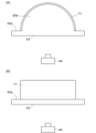
- the building material 30 is, for example, as shown in FIG. 9(A), wall surfaces, ceiling surfaces, floor surfaces of rooms and corridors, wallpaper for partitions, decorative materials 30A such as posters, and decorative materials such as transparent stickers for light covers.
- 30B can be installed in a building.
- the radio wave reflector 11 may be formed as a member made of a non-conductive material such as resin or held inside a building material.
- the wall surface 31 itself, which is the building material 30 , or the lamp cover 32 itself may be composed of the radio wave reflector 11 .
- the building material 30 is not limited to indoor walls and light covers, and may be, for example, partitions, pillars, lintels, outer walls of buildings, windows, and the like.
- FIG. 9B is a plan view of the interior of the room, and the building material 30, which is the radio wave reflector 11, is formed as a corner pillar 30C having a curved surface at the corner of the room. The radio wave entering from the window 33 is reflected by the corner post 30C and reaches a wider range of the indoor space S.
- 9(A) and 9(B) show an application example of the building material 30, and do not show the actual range of radio wave reflection.
- Examples 1 to 9 were produced as the radio wave reflector 11, and evaluation tests were conducted on the reflection direction correctability and irregularity followability for Examples 1 to 9 and Comparative Examples 1 to 4.
- the radio wave reflector 11 of the present invention is not limited to Examples 1-9.
- Example 1 shows the details of Examples 1 to 9 and Comparative Examples 1 to 4 and the results of evaluation tests.
- Examples 1 to 9 and Comparative Examples 1 to 4 have any one of "configuration A” to "configuration D” and "metal plate” as the configuration of the radio wave reflector.
- Configuration A is a configuration in which a substrate layer 13, a conductive thin film layer 16 (conductor 12), an adhesive layer 14, and a protective layer 15 are laminated in order, as in the embodiment shown in FIGS.
- a synthetic resin material sheet made of PET as the substrate layer 13 and the protective layer 15 (manufactured by Toray Industries, Lumirror 50T60, product number #125-U34 when the thickness of the substrate layer 13 and protective layer 15 is 0.13 mm, thickness 0.13 mm). In the case of 19 mm, product number #188-U34) was used.
- Configuration B is a configuration in which a conductive thin film layer 16 (conductor 12) is laminated on a base material layer 13, as in the embodiment shown in FIG.
- a synthetic resin material sheet TOMBP No. 9000 manufactured by NICHIAS Corporation
- PTFE fluororesin
- Configuration C is a configuration in which a conductive thin film layer 16 (conductor 12) is laminated on a substrate layer 13, as in the embodiment shown in FIG. G-Leaf manufactured by Electric Glass Co., Ltd.) was used.
- Configuration D is a configuration in which a base layer 13, a conductive thin film layer 16 (conductor 12), an adhesive layer 14, and a protective layer 15 are laminated in order, as in the embodiment shown in FIGS.
- the substrate layer 13 is different from that of configuration A.
- a synthetic resin material sheet Midfil NS manufactured by Kurashiki Boseki Co., Ltd.
- PEEK polyetheretherketone
- Metal plate is a structure consisting of a single metal plate.
- connection type means that, as shown in FIGS. 3B and 4, one or a plurality of linear conductors 12 are arranged surrounding a region 12a where there are no conductors 12, that is, , conductors 12 and areas 12a without conductors 12 are periodically arranged at predetermined intervals.
- isolated type means that sheet-shaped conductors 12 are periodically arranged as shown in FIG. 5 or 6 .
- the shape of the arrangement pattern of the conductors 12 is shown as “zigzag”, “lattice”, and “circular”. “Staggered” means that the arrangement pattern of the conductors 12 is “connected”, and the conductors 12 are staggered as shown in FIG. 4(A).
- the “lattice pattern” is a case where the arrangement pattern of the conductors 12 is “connected type”, and the conductors 12 are arranged at equal intervals along the vertical and horizontal directions as shown in FIG. 3B.
- the shape is "Circular” means that the arrangement pattern of the conductors 12 is “isolated”, and the shape of each conductor 12 is circular as shown in FIG.
- the adhesive used for the adhesive layer 14 is shown as "rubber-based” and "acrylic-based".
- rubber-based is meant a rubber-based adhesive.
- the rubber-based adhesive was obtained by the following method. A reaction vessel equipped with a cooling tube, a nitrogen inlet tube, a thermometer, a dropping funnel and a stirring device was charged with a rubber-based polymer (styrene-(ethylene-propylene)-styrene type block copolymer 50% by mass and styrene-(ethylene-propylene ) type block copolymer 50% by mass, styrene content 15%, weight average molecular weight 130,000) 100 parts by weight, synthetic resin (manufactured by Mitsui Chemicals, FMR-0150) 40 parts by weight, softener (JX Nikko Nisseki Energy Co., Ltd., LV-100) 20 parts by weight, antioxidant (ADEKA Co., Ltd., Adekastab AO-330) 0.5 parts by weight and to
- Acrylic refers to acrylic adhesives.
- the acrylic adhesive was obtained by the following method. Monofunctional long-chain urethane acrylate (PEM-X264 manufactured by AGC, molecular weight 10000) 40 parts by weight, and acrylic monomer 60 parts by weight (2-ethylhexyl acrylate (2EHA) 35 parts by weight, cyclohexyl acrylate (CHA) 10 parts by weight, 2-hydroxy 10 parts by mass of ethyl acrylate (2HEA) and 5 parts by mass of dimethylacrylamide (DMAA)) were mixed and stirred.
- PEM-X264 Monofunctional long-chain urethane acrylate
- EHA 2-ethylhexyl acrylate
- CHA cyclohexyl acrylate
- 2-HEA 2-hydroxy 10 parts by mass of ethyl acrylate
- DMAA dimethylacrylamide
- a crosslinking agent (1.6 hexanediol diacrylate (A-HD -N, manufactured by Shin Nakamura Chemical Co., Ltd.)) and a photopolymerization initiator (Omnirad 651 (manufactured by IGM Japan LLC)) were added, stirred, and vacuum degassed. An acrylic adhesive was thus obtained.
- a crosslinking agent 1.6 hexanediol diacrylate (A-HD -N, manufactured by Shin Nakamura Chemical Co., Ltd.)
- a photopolymerization initiator (Omnirad 651 (manufactured by IGM Japan LLC)
- the adhesive layer 14 has a dielectric loss tangent value of 0.002, which is 0.018 or less.
- the radio wave reflector 11 produced as Example 1 has the configuration of "Configuration A”.
- the radio wave reflector 11 has a square planar shape, a side length L10 of 100 cm, and a thickness L11 of 0.4 mm.
- the radio wave reflection intensity in a flat state ("specular reflection intensity at 28.5 GHz in a flat state” in Table 1) is -24 dB, the Young's modulus is 0.08 GPa, the bending elastic modulus is 2.2 GPa, and the surface resistivity is 1.7 ⁇ / ⁇ , and the rate of change R of the surface resistivity during bending is 4.3%.
- the radio wave reflector 11 has a total light transmittance of 89%.
- the thickness L8 of the base material layer 13 is 0.13 mm.
- the arrangement pattern of the conductors 12 of the conductive thin film layer 16 is a connected type, and the arrangement pattern is staggered.
- the line width L6 of the conductor 12 is 400 nm, the thickness L3 of the conductor 12 is 0.4 ⁇ m, and the interval L7 between the adjacent conductors 12 is 100 ⁇ m (tolerance ⁇ 10 ⁇ m, the same applies hereinafter).
- the conductor 12 is a metal thin film made of silver (Ag).
- the conductive thin film layer 16 has a surface roughness Sa of 1.1 ⁇ m and a coverage of 0.80%.
- the adhesive layer 14 is made of rubber, the thickness L4 of the adhesive layer 14 is 0.04 mm, and the thickness L5 of the protective layer 15 is 0.13 mm.
- the conductor 12 is formed on the base layer 13 .
- a core layer of 0.01 ⁇ m or more and 3 ⁇ m or less is formed on one surface of a copper foil having a thickness of 5 ⁇ m or more and 200 ⁇ m or less, which has sufficient strength as a metal layer, by a method such as electrolytic or electroless plating.
- a conductive thin film layer 16 having a predetermined arrangement pattern is formed on the surface of the core layer by a method such as electrolytic or electroless plating.
- the entire conductive thin film layer 16 is covered with the base material layer 13 .
- An adhesive is applied to the base layer 13 in advance.
- the copper foil and core layer are removed by etching. Thereby, the conductor 12 is formed on the base material layer 13 .
- the protective layer 15 is attached to the side of the conductor 12 opposite to the base layer 13 by the adhesive layer 14 .
- the protective layer 15 is adhered onto the conductor 12 of the substrate layer 13 so as to prevent air bubbles from entering.
- the radio wave reflector 11 is manufactured.
- the radio wave reflector 11 produced as Example 2 has the configuration of "Configuration B" and does not include the adhesive layer 14 and the protective layer 15.
- the thickness L11 of the radio wave reflector 11 is 0.08 mm.
- the radio wave reflection intensity in the flat state is -23 dB
- the Young's modulus is 0.5 GPa
- the flexural modulus is 0.6 GPa
- the surface resistivity is 1.4 ⁇ / ⁇
- the change rate R of the surface resistivity when bending is 2.0. 8%.
- the radio wave reflector 11 has a total light transmittance of 0.1%.
- the thickness L8 of the base material layer 13 is 0.08 mm.
- the arrangement pattern of the conductors 12 of the conductive thin film layer 16, the shape of the arrangement pattern, the line width L6, the thickness L3, the interval L7 between the adjacent conductors 12, the materials of the conductors, and other configurations are the same as in the first embodiment. be.
- the radio wave reflector 11 of Example 2 is manufactured in the same manner as in Example 1, but the adhesive layer 14 and protective layer 15 are not provided.
- the radio wave reflector 11 produced as Example 3 has the same "configuration A" as Example 1.
- the thickness L11 of the radio wave reflector 11 is 0.5 mm.
- the radio wave reflection intensity in the flat state is -25 dB
- the Young's modulus is 0.08 GPa
- the bending elastic modulus is 2.2 GPa
- the surface resistivity is 1.5 ⁇ / ⁇
- the surface resistivity change rate R during bending is 9.0. 8%.
- the radio wave reflector 11 has a total light transmittance of 87%.
- the thickness L8 of the base material layer 13 is 0.19 mm.
- the adhesive layer 14 is made of rubber, the thickness L4 of the adhesive layer 14 is 0.12 mm, and the thickness L5 of the protective layer 15 is 0.19 mm.
- the arrangement pattern of the conductors 12 of the conductive thin film layer 16 the shape of the arrangement pattern, the line width L6, the thickness L3, the interval L7 between the adjacent conductors 12, the materials of the conductors, and other configurations are the same as in the first embodiment. be.
- the radio wave reflector 11 produced as Example 4 has the configuration of "Configuration C" and does not include the adhesive layer 14 and the protective layer 15.
- the thickness L11 of the radio wave reflector 11 is 0.05 mm.
- the radio wave reflection intensity in the flat state is -26 dB
- the Young's modulus is 70 GPa
- the bending elastic modulus is 0.05 GPa
- the surface resistivity is 3.8 ⁇ / ⁇
- the surface resistivity change rate R during bending is 3.9%. is.
- the radio wave reflector 11 has a total light transmittance of 90%.
- the thickness L8 of the base material layer 13 is 0.05 mm.
- the arrangement pattern of the conductors 12 of the conductive thin film layer 16 is a connected type, and the arrangement pattern has a lattice shape.
- the radio wave reflector 11 of Example 4 is manufactured in the same manner as in Example 1, but the adhesive layer 14 and protective layer 15 are not provided.
- the radio wave reflector 11 produced as Example 5 has the configuration of "configuration D".
- the thickness L11 of the radio wave reflector 11 is 0.5 mm.
- the radio wave reflection intensity in the flat state is -25 dB
- the Young's modulus is 0.1 GPa
- the bending elastic modulus is 3.7 GPa
- the surface resistivity is 2.1 ⁇ / ⁇
- the surface resistivity change rate R during bending is 9.0. 5%.
- the radio wave reflector 11 has a total light transmittance of 0.1%.
- the thickness L8 of the base material layer 13 is 0.25 mm.
- the arrangement pattern of the conductors 12 of the conductive thin film layer 16 is a connected type, and the arrangement pattern has a lattice shape.
- the adhesive layer 14 is made of rubber, the thickness L4 of the adhesive layer 14 is 0.06 mm, and the thickness L5 of the protective layer 15 is 0.19 mm.
- Other configurations such as the line width L6 and thickness L3 of the conductors 12, the spacing L7 between the adjacent conductors 12, and the materials of the conductors are the same as those of the first embodiment.
- the radio wave reflector 11 produced as Example 6 has the configuration of "configuration A".
- the radio wave reflection intensity in the flat state is -27 dB
- the Young's modulus is 0.08 GPa
- the flexural modulus is 2.2 GPa
- the surface resistivity is 0.003 ⁇ / ⁇
- the surface resistivity change rate R during bending is 1.5. 1%.
- the radio wave reflector 11 has a total light transmittance of 80%.
- the arrangement pattern of the conductors 12 of the conductive thin film layer 16 is an isolated type, and the arrangement pattern has a circular shape.
- the thickness L3 of the conductors 12 is 0.5 ⁇ m, the diameter L1 of the conductors 12 is 1000 ⁇ m, and the interval L2 between adjacent conductors 12 is 10 ⁇ m (tolerance ⁇ 10 ⁇ m, same below).
- the conductive thin film layer 16 has a surface roughness Sa of 2.3 ⁇ m and a coverage of 23%. Other configurations are the same as those of the first embodiment.
- a method of manufacturing the radio wave reflectors 11 of Examples 6 and 7 and Comparative Example 3 will be described.
- the conductor 12 is formed on the base layer 13 .
- a roll-to-roll type sputtering apparatus is used.
- a target containing a metal for example, silver
- a ground shield is provided in such a size that 5% of the cathode is covered with respect to the cathode.
- a film forming chamber of the sputtering apparatus is evacuated by a vacuum pump, the pressure is reduced to 3.0 ⁇ 10 ⁇ 4 Pa, for example, and argon gas is supplied at a predetermined flow rate (100 sccm), for example.
- the substrate layer 13 is conveyed under the cathode at a conveying speed of 0.1 m/min and a tension of 100 N, for example.
- a pulsed power of 5 kW is supplied from a bipolar power supply connected to the cathode, whereby metal is ejected from the target and deposited on the surface of the substrate layer 13, thereby forming a metal thin film.
- a mask is formed in the arrangement pattern of the conductors 12 on the surface of the metal thin film by photolithography.
- a chemical is used to remove the unmasked portion of the metal thin film.
- the conductor 12 is then formed by removing the masked portion. Thereby, a conductive thin film layer 16 having a plurality of conductors 12 is formed on the substrate layer 13 .
- the evaluation of whether or not the metal thin film is formed with the desired thickness is performed, for example, by the following procedure.
- a nanoindenter TI950, manufactured by HYSITRON
- HYSITRON a nanoindenter
- the thickness of the metal thin film is measured from the gap caused by the indentation.
- the average film thickness and standard deviation from the measured values of about 30 locations, whether the average film thickness is the desired thickness L3 (e.g., 50 nm), and the variation in the measured values is within the desired range (e.g., the standard deviation is within 5).
- the protective layer 15 is attached to the conductor 12 with the adhesive layer 14 .
- the protective layer 15 is adhered onto the conductor 12 of the substrate layer 13 so as to prevent air bubbles from entering.
- the radio wave reflector 11 is manufactured.
- the radio wave reflector 11 produced as Example 7 has the configuration of "configuration A".
- the radio wave reflection intensity in the flat state is -29 dB
- the Young's modulus is 0.08 GPa
- the flexural modulus is 2.2 GPa
- the surface resistivity is 9.8 ⁇ / ⁇
- the surface resistivity change rate R during bending is 1.0. 2%.
- the radio wave reflector 11 has a total light transmittance of 79%.
- the arrangement pattern of the conductors 12 of the conductive thin film layer 16 is an isolated type, and the arrangement pattern has a circular shape.
- the thickness L3 of the conductor 12 is 0.04 ⁇ m
- the diameter L1 of the conductor 12 is 1000 ⁇ m
- the interval L2 between adjacent conductors 12 is 10 ⁇ m.
- the conductor 12 is a metal thin film made of titanium.
- the conductive thin film layer 16 has a surface roughness Sa of 3.1 ⁇ m and a coverage of 23%. Other configurations are the same
- the radio wave reflector 11 produced as Example 8 has the configuration of "configuration D".
- the bending elastic modulus is 3.9 GPa, and the rate of change R of the surface resistivity during bending is 9.6%.
- Other configurations are the same as those of the fifth embodiment.
- the radio wave reflector 11 produced as Example 9 has an acrylic adhesive layer 14 .
- Other configurations are the same as those of the third embodiment.
- the radio wave reflector created as Comparative Example 1 is a single metal plate made of aluminum with a thickness of 0.5 mm.
- the radio wave reflection intensity in the flat state is -24 dB
- the Young's modulus is 70 GPa
- the bending elastic modulus is 71 GPa
- the surface resistivity is 0.00005 ⁇ / ⁇
- the surface resistivity change rate R during bending is 0.1%.
- the radio wave reflector 11 has a total light transmittance of 0% and a surface roughness Sa of 1.06 ⁇ m.
- the radio wave reflector produced as Comparative Example 2 has the configuration of "Configuration B" and does not include the adhesive layer 14 and the protective layer 15.
- the thickness L11 of the radio wave reflector 11 is 0.6 mm.
- the radio wave reflection intensity is -23 dB
- the Young's modulus is 0.5 GPa
- the bending elastic modulus is 0.6 GPa
- the surface resistivity is 1.4 ⁇ / ⁇ .
- the surface resistivity of the radio wave reflector bent along a curved surface with a radius of curvature of 200 mm could not be measured because the radio wave reflector 11 was damaged during bending. is not measurable.
- the radio wave reflector 11 has a total light transmittance of 0%.
- the thickness L8 of the base material layer 13 is 0.6 mm.
- the arrangement pattern of the conductors 12 of the conductive thin film layer 16, the shape of the arrangement pattern, the line width L6, the thickness L3, the interval L7 between the adjacent conductors 12, the materials of the conductors, and other configurations are the same as in the first embodiment. be.
- the radio wave reflector 11 of Comparative Example 2 is manufactured in the same manner as in Example 1, but the adhesive layer 14 and the protective layer 15 are not provided, and the thickness of the base layer 13 is greater than that of Example 2. set large.
- the radio wave reflector created as Comparative Example 3 has the configuration of "configuration A".
- the radio wave reflection intensity in the flat state is -38 dB
- the Young's modulus is 0.08 GPa
- the bending elastic modulus is 2.2 GPa
- the surface resistivity is 20.5 ⁇ / ⁇
- the surface resistivity change rate R is 0.6%. be.
- the radio wave reflector 11 has a total light transmittance of 80%.
- the arrangement pattern of the conductors 12 of the conductive thin film layer 16 is an isolated type, and the arrangement pattern has a circular shape.
- the thickness L3 of the conductor 12 is 0.02 ⁇ m
- the diameter L1 of the conductor 12 is 1000 nm
- the interval L2 between adjacent conductors 12 is 10 ⁇ m.
- the conductor 12 is a metal thin film made of titanium.
- the conductive thin film layer 16 has a surface roughness Sa of 2.6 ⁇ m and a coverage of 23%. Other configurations are the same as those of the
- the radio wave reflector created as Comparative Example 4 has the configuration of "configuration D". In a flat state, the radio wave reflection intensity is -31 dB, the Young's modulus is 0.8 GPa, the bending elastic modulus is 4.2 GPa, and the surface resistivity change rate R is 13%.
- the radio wave reflector 11 has a total light transmittance of 80%. Other configurations are the same as those of the fifth embodiment.
- a continuously changing radio wave with a frequency of 3 to 300 GHz was output from the transmitting antenna, and the amount of reflection (reflection intensity) of the radio wave was measured.
- the amount of reflection at a frequency of 28.5 GHz and the frequency band where the amount of reflection is -30 dB or more were determined.
- a reference metal plate (aluminum A1050 plate, thickness 3 mm) was placed on the sample stand, and the reception level was measured and recorded using a scalar network analyzer.
- the coaxial cables of the receiving antenna and the transmitting antenna were directly connected by a scalar network analyzer, and the signal level at each frequency was calibrated as 0.
- the device was reconfigured and measurements were taken.
- the reference metal plate was removed from the sample mount, the sample was placed on the sample mount, and the reception level was measured and recorded. By subtracting the reception level of the reference metal plate from the measured reception level, the reflection amount in the specular direction of the radio wave reflector 11 to be measured was obtained. Similar measurements were repeated for each sample.
- the frequency of the radio wave was 10 GHz or less
- the sample was irradiated with a plane wave using an appropriate millimeter wave lens in consideration of the first Fresnel radius of the rectangular horn antenna.
- the surface resistivity R1 of the radio wave reflector 11 when the radio wave reflector 11 is flattened is measured by the four-terminal method specified in JIS K7194: 1994 by contacting a measuring terminal to the surface of the conductive thin film layer 16 made of the conductor 12. Measured according to In addition, when the conductive thin film layer 16 is protected by a resin sheet or the like and is not exposed, the eddy current is measured using a non-contact resistance measuring device (manufactured by Napson Co., Ltd., trade name: EC-80P, or its equivalent). measured by the method. The surface resistivity of the conductive thin film layer 16 is shown as the surface resistivity of the radio wave reflector 11 .
- each conductor 12 has a circular shape with a diameter of 1000 nm in plan view, and the surface resistivities R1 and R2 of each conductor 12 are measured. However, when the area of each conductor 12 in a plan view is about several centimeters square, the surface resistivities R1 and R2 are measured for the entire conductive thin film layer 16 as a measurement object.
- the flexural modulus is measured according to JIS K7171, and the Young's modulus is measured according to JIS K7127-1999.
- Reflection direction correctability is achieved by bending the radio wave reflector 11 when installing it in a direction rotated by a certain rotation angle around the reflection point with respect to the specular reflection direction. can reflect radio waves in a desired direction with a practically acceptable reflection intensity.
- the evaluation method for correcting the direction of reflection is as follows. As shown in FIG. 10, the radio wave reflector 11 is placed on an installation surface 42 that has a flat surface and is parallel to the horizontal direction, and the radio wave reflector 11 is aligned along a line (center line) passing through the center points of opposite sides of a square. fold along.
- the bending angle ⁇ 3 between the installation surface 42 and the reflection surface of the radio wave reflector 11 is assumed to be 10 degrees.
- the transmitting antenna 40 is installed so that the incident angle ⁇ 1 of the incident wave is 60 degrees.
- the distance between the reflection point 11a and the transmitting antenna 40 is set to 5m.
- the receiving antenna 41 which is the receiving unit 21, is installed at a clockwise rotation angle ⁇ 4 in FIG. 10 when the normal line 22 is 0 degrees, and the rotation angle ⁇ 4 is 50 degrees. That is, the installation position of the receiving antenna 41 is set so that the direction of specular reflection (arrow A3) when the radio wave reflector 11 is flatly installed on the installation surface 42 is perpendicular to the normal line 22 by a rotation angle of 10 degrees around the reflection point 11a. It is a close position. The distance between the reflection point 11a and the receiving antenna 41 is set to 5 m.
- a radio wave with a frequency of 28 GHz was output from the transmitting antenna 40, and the amount of reflection (reflection intensity) at the receiving antenna 41 was measured.
- the method for measuring the reflection intensity is the same as the method for measuring the reflection intensity described above.
- the reception strength of the radio wave of the receiving antenna 41 was ⁇ 30 dB or more, it was evaluated as “ ⁇ ”, and when it was less than ⁇ 30 dB, it was evaluated as “ ⁇ ”.
- a test stand 43 was prepared which has a convex portion 43b projecting upward from the upper surface of a plate-like portion 43a.
- the convex portion 43b has a semi-cylindrical cross-sectional shape with a radius of 200 mm (curved surface with a radius of curvature of 200 mm).
- the test table 43 is transparent as a whole, and the total light transmittance is 75% at the longest vertical length in the side view of the test table 43 shown in FIG.
- An image capturing device 44 such as a camera is arranged below the test table 33 .
- An adhesive (PPX manufactured by Cemedine Co., Ltd.) was applied to the surface of the convex portion 43b of the test table 43 so that the substrate layer 13 of the radio wave reflector 11 was in contact, and the conductor 12 was passed through the test table 43 by the imaging device 44. to shoot.
- the obtained images are computer-analyzed using image processing software (AVizo manufactured by THERMO FISHER SCIENTIFIC).
- the area where the radio wave reflector 11 and the convex portion 43b of the test table 43 overlap that is, the area of the radio wave reflector 11
- the area of the existing air bubbles is obtained, and the area of the air bubbles is subtracted from the area of the radio wave reflector 11 to calculate the area where the radio wave reflector 11 is in close contact with the convex portion 43b with the adhesive. If the ratio of the area where the radio wave reflector 11 is in close contact with the convex portion 43b is 90% or more of the area of the radio wave reflector 11, it is evaluated as " ⁇ ", and if it is less than 90%, it is evaluated as "X". bottom. “Close contact” means that an adhesive exists between the surface of the convex portion 43b and the radio wave reflector 11, but air bubbles do not exist.
- Table 1 shows the evaluation results.
- the specular reflection intensity when the radio wave reflector 11 is flattened is -30 dB or more
- the reflection direction correctability is evaluated as " ⁇ ”
- the unevenness followability is evaluated as " ⁇ ”.
- Comparative Example 1 was composed of an aluminum plate, had a specular reflection intensity of more than -30 dB, and was evaluated as " ⁇ " in the reflection direction correctability, but could not be curved and had an "X" in the irregularity followability. ” was the evaluation.
- Comparative Example 2 the thickness of the base layer 13 is set larger than that in Example 2, and although the specular reflection intensity is greater than ⁇ 30 dB, the reflection direction correctability is evaluated as “ ⁇ ” and bending cannot be performed. The irregularity followability was evaluated as "x”.
- Comparative Example 3 the thickness L3 of the conductor 12 was set to be smaller than that in Example 7, and sufficient specular reflection intensity could not be ensured, and the reflection direction correctability was evaluated as "x”.
- Comparative Example 4 had a higher flexural modulus than Example 5, could not be bent, and was evaluated as "poor” in conformability to irregularities.
Landscapes
- Physics & Mathematics (AREA)
- Electromagnetism (AREA)
- Aerials With Secondary Devices (AREA)
Abstract
Provided are: a radio wave reflector that is flexible and reflects radio waves while maintaining the intensity thereof; and a construction material. The radio wave reflector 11 that reflects radio waves is such that: when the radio wave reflector 11 is in a flat state and a radio wave is reflected by the radio wave reflector 11 at an incidence angle of an incident wave of 15-75 degrees, there is at least one frequency at which the intensity of the reflected wave when the incident wave is regularly reflected is -30 dB or greater relative to the intensity of the incident wave; and in relation to a surface resistivity R1 of the radio wave reflector 11 when the radio wave reflector 11 is in a flat state, a change rate of a surface resistivity R2 when the radio wave reflector 11 is in a curved state along a curved surface having a curvature radius of 200 mm is -10% to 10%, inclusive, and the flexural modulus thereof is 0.05-4 GPa.
Description
本発明は、電波を反射させるための電波反射体および建築材料に関する。
The present invention relates to radio wave reflectors and building materials for reflecting radio waves.
携帯電話や無線通信においては、2GHz以上300GHz以下程度の周波数帯の電波が用いられる。このような波長が短い電波は直進性が強く、障害物があっても回り込みにくいため、電波を広い範囲に届かせるために、反射板が用いられる。例えば特許文献1には、モノポールアンテナと、電波を反射する金属反射板とを屋内の床下空間に配置した通信システムが提案されている。特許文献1においては、モノポールアンテナから放射される電波を床下空間に拡散させるとともに、床下空間から居室(建物)外に漏洩したり、建造物の床部に電波が吸収されることを防いでいる。
In mobile phones and wireless communications, radio waves in the frequency band of about 2 GHz to 300 GHz are used. Radio waves with such short wavelengths travel in a straight line and are difficult to circulate even if there is an obstacle. For example, Patent Literature 1 proposes a communication system in which a monopole antenna and a metal reflector that reflects radio waves are arranged in an indoor underfloor space. In Patent Document 1, radio waves radiated from a monopole antenna are diffused in an underfloor space, and are prevented from leaking from the underfloor space to the outside of a living room (building) or being absorbed by the floor of a building. there is
電波を反射させる金属反射板は、一般的に、アルミニウムや銅等の金属板から構成される。金属反射板は、波長の短い電波の場合、正反射方向には強い強度で電波を反射させるが、拡散させて反射させにくく、空間の広い範囲に電波が届きにくいことが知られている。空間の所望の範囲に電波を届かせるために、居室の壁や柱等の設置面に適切な角度で金属反射板を貼付け、電波を所望の方向に反射させる。
A metal reflector that reflects radio waves is generally composed of a metal plate such as aluminum or copper. It is known that metal reflectors reflect radio waves with a high intensity in the direction of specular reflection in the case of radio waves with short wavelengths, but they are difficult to diffuse and reflect, making it difficult for radio waves to reach a wide range of space. In order for radio waves to reach a desired range in space, a metal reflector is attached at an appropriate angle to an installation surface such as a wall or a pillar in a living room to reflect radio waves in a desired direction.
金属反射板は一般的に可撓性を有しておらず剛性が高いため、壁や柱等の設置面が曲面の場合は、金属反射板を貼り付けることができない。また、設置面に凹凸があると、金属反射板の反射面をわずかに傾けるなどの微調整ができず、金属反射板の反射面の角度が所望の角度と大きくずれてしまう。このように、金属反射板に可撓性がないために、居室内で電波反射のための環境を整えにくいという問題があった。
Since metal reflectors generally do not have flexibility and have high rigidity, metal reflectors cannot be attached to curved surfaces such as walls and pillars. Further, if the installation surface has unevenness, fine adjustment such as tilting the reflecting surface of the metal reflecting plate is not possible, and the angle of the reflecting surface of the metal reflecting plate greatly deviates from the desired angle. As described above, since the metal reflector is not flexible, there is a problem that it is difficult to prepare an environment for radio wave reflection in the living room.
本発明は、電波の強度を保ちながら電波を反射させ、かつ可撓性を有する電波反射体および建築材料を提供することを目的とする。
An object of the present invention is to provide a flexible radio wave reflector and a building material that reflect radio waves while maintaining the strength of the radio waves.
上記目的を達成するため、本発明は、次の項に記載の主題を包含する。
In order to achieve the above objectives, the present invention includes the subjects described in the following sections.
項1.電波を反射させる電波反射体であって、
前記電波反射体を平らとした状態で、前記電波反射体に、入射波の入射角が15度以上75度以下の角度で、電波を反射させたときに、前記入射波が正反射したときの反射波の強度が前記入射波の強度に対して-30dB以上となる周波数が存在し、
前記電波反射体を平らとした状態の電波反射体の表面抵抗率に対して、前記電波反射体を曲率半径200mmの曲面に沿って湾曲させた状態の表面抵抗率の変化率は、-10%以上10%以下であり、
曲げ弾性率が0.05GPa以上4GPa以下である、電波反射体。Section 1. A radio wave reflector that reflects radio waves,
When the radio wave reflector is flattened and the radio wave is reflected by the radio wave reflector at an incident angle of 15 degrees or more and 75 degrees or less, the incident wave is specularly reflected. There is a frequency at which the intensity of the reflected wave is -30 dB or more with respect to the intensity of the incident wave,
With respect to the surface resistivity of the radio wave reflector in the flat state, the change rate of the surface resistivity in the state where the radio wave reflector is curved along a curved surface with a radius of curvature of 200 mm is −10%. not less than 10%,
A radio wave reflector having a flexural modulus of 0.05 GPa or more and 4 GPa or less.
前記電波反射体を平らとした状態で、前記電波反射体に、入射波の入射角が15度以上75度以下の角度で、電波を反射させたときに、前記入射波が正反射したときの反射波の強度が前記入射波の強度に対して-30dB以上となる周波数が存在し、
前記電波反射体を平らとした状態の電波反射体の表面抵抗率に対して、前記電波反射体を曲率半径200mmの曲面に沿って湾曲させた状態の表面抵抗率の変化率は、-10%以上10%以下であり、
曲げ弾性率が0.05GPa以上4GPa以下である、電波反射体。
When the radio wave reflector is flattened and the radio wave is reflected by the radio wave reflector at an incident angle of 15 degrees or more and 75 degrees or less, the incident wave is specularly reflected. There is a frequency at which the intensity of the reflected wave is -30 dB or more with respect to the intensity of the incident wave,
With respect to the surface resistivity of the radio wave reflector in the flat state, the change rate of the surface resistivity in the state where the radio wave reflector is curved along a curved surface with a radius of curvature of 200 mm is −10%. not less than 10%,
A radio wave reflector having a flexural modulus of 0.05 GPa or more and 4 GPa or less.
項2.入射波の周波数が2GHz以上300GHz以下の任意の周波数である、項1に記載の電波反射体。
Section 2. Item 2. The radio wave reflector according to item 1, wherein the frequency of the incident wave is any frequency of 2 GHz or more and 300 GHz or less.
項3.ヤング率が0.01GPa以上80GPa以下である、項1または2に記載の電波反射体。
Item 3. Item 3. The radio wave reflector according to item 1 or 2, which has a Young's modulus of 0.01 GPa or more and 80 GPa or less.
項4.前記電波反射体の厚みが0.01mm以上0.5mm以下である、項1から3のいずれか1項に記載の電波反射体。
Section 4. 4. The radio wave reflector according to any one of items 1 to 3, wherein the radio wave reflector has a thickness of 0.01 mm or more and 0.5 mm or less.
項5.電波を反射させる前記導電体を含む導電薄膜層と、前記導電薄膜層に積層され、基材を含む基材層とを少なくとも有する、項1から4のいずれか1項に記載の電波反射体。
Item 5. 5. The radio wave reflector according to any one of items 1 to 4, comprising at least a conductive thin film layer containing the conductor that reflects radio waves, and a substrate layer laminated on the conductive thin film layer and containing a substrate.
項6.電波を反射させる導電体を含む導電薄膜層と、前記導電薄膜層に積層され、基材を含む基材層と、前記導電薄膜層を保護するための保護材を含む保護層と、前記導電薄膜層と前記保護材を含む層とを接着するための接着剤を含む接着層とを有し、
前記基材層、前記導電薄膜層、前記接着層、前記保護層の順に積層されている、項1から5のいずれか1項に記載の電波反射体。 Item 6. A conductive thin film layer containing a conductor that reflects radio waves, a base layer laminated on the conductive thin film layer and containing a base material, a protective layer containing a protective material for protecting the conductive thin film layer, and the conductive thin film an adhesive layer containing an adhesive for bonding the layer and the layer containing the protective material;
Item 6. The radio wave reflector according to any one ofItems 1 to 5, wherein the substrate layer, the conductive thin film layer, the adhesive layer, and the protective layer are laminated in this order.
前記基材層、前記導電薄膜層、前記接着層、前記保護層の順に積層されている、項1から5のいずれか1項に記載の電波反射体。 Item 6. A conductive thin film layer containing a conductor that reflects radio waves, a base layer laminated on the conductive thin film layer and containing a base material, a protective layer containing a protective material for protecting the conductive thin film layer, and the conductive thin film an adhesive layer containing an adhesive for bonding the layer and the layer containing the protective material;
Item 6. The radio wave reflector according to any one of
項7.前記電波反射体を平らとした状態の表面抵抗率が0.003Ω/□以上、10Ω/□以下である、項1から6のいずれか1項に記載の電波反射体。
Item 7. Item 7. The radio wave reflector according to any one of items 1 to 6, wherein the surface resistivity of the radio wave reflector in a flat state is 0.003 Ω/□ or more and 10 Ω/□ or less.
項8.前記保護層は、アンチグレア処理またはアンチリフレクション処理が施されている、項6に記載の電波反射体。
Item 8. Item 7. The radio wave reflector according to Item 6, wherein the protective layer is subjected to anti-glare treatment or anti-reflection treatment.
項9.項1から8のいずれか1項に記載の電波反射体を含む建築材料。
Item 9. A building material comprising the radio wave reflector according to any one of Items 1 to 8.
本発明によれば、電波の強度を保ちながら電波を反射させ、かつ可撓性を有する電波反射体を提供することができる。
According to the present invention, it is possible to provide a flexible radio wave reflector that reflects radio waves while maintaining the strength of the radio waves.
(全体構成)
本発明の実施形態を図面を参照して説明する。本実施形態の電波反射体11は、図1に示すように、電波発生源20から出力された電波を反射する。反射された反射波は、受信部21により受信される。電波発生源20は電波を送信可能な送信アンテナを持つ通信装置等である。受信部21は、電波を受信可能な機器である。本実施形態に係る受信部21は、受信アンテナを持つ通信機器である。通信機器としては、例えば、スマートフォン、携帯電話、タブレット端末、ノートPC、携帯ゲーム機、中継器、ラジオ、テレビ等が挙げられる。 (overall structure)
An embodiment of the present invention will be described with reference to the drawings. Theradio wave reflector 11 of this embodiment reflects radio waves output from the radio wave source 20, as shown in FIG. The reflected wave is received by the receiver 21 . The radio wave source 20 is a communication device or the like having a transmission antenna capable of transmitting radio waves. The receiver 21 is a device capable of receiving radio waves. The receiving unit 21 according to this embodiment is a communication device having a receiving antenna. Examples of communication devices include smartphones, mobile phones, tablet terminals, notebook PCs, portable game machines, repeaters, radios, and televisions.
本発明の実施形態を図面を参照して説明する。本実施形態の電波反射体11は、図1に示すように、電波発生源20から出力された電波を反射する。反射された反射波は、受信部21により受信される。電波発生源20は電波を送信可能な送信アンテナを持つ通信装置等である。受信部21は、電波を受信可能な機器である。本実施形態に係る受信部21は、受信アンテナを持つ通信機器である。通信機器としては、例えば、スマートフォン、携帯電話、タブレット端末、ノートPC、携帯ゲーム機、中継器、ラジオ、テレビ等が挙げられる。 (overall structure)
An embodiment of the present invention will be described with reference to the drawings. The
電波反射体11は、電波を反射させる導電体12を含む。電波反射体11を平らとした状態で、入射波の入射角が15度以上75度以下の少なくともある所定の角度で、好ましくは、45度、より好ましくは15度以上75度以下の角度の範囲全てにおいて、入射波の周波数が2GHz以上6GHz未満、6GHz以上20GHz未満、20GHz以上60GHz未満、60GHz以上100GHz未満、100GHz以上150GHz未満、または150GHz以上300GHz以下の電波を電波反射体11に反射させる。このとき、電波反射体11に入射波が正反射したときの反射波の強度(以下、「正反射強度」ともいう。)が入射波に対して-30dB以上0dB以下となる周波数が少なくとも一つ存在する。好ましくは、周波数28.5GHzにおいて、正反射強度が入射波に対して-30dB以上0dB以下となり、より好ましくは20GHz以上60GHz以下の周波数帯域全てにおいて、正反射強度が入射波に対して-30dB以上0dB以下となり、更に好ましくは2GHz以上、300GHz以下の周波数帯域全てにおいて、正反射強度が入射波に対して-30dB以上0dB以下となる。「正反射強度」とは、電波が反射する強度である反射強度であって、入射波が正反射したときの反射波の強度をいう。「平ら」とは、凹凸がなく湾曲していない状態か、凹凸があった場合であっても、表面上の任意の点の曲率半径が1000mm以上の状態をいう。
The radio wave reflector 11 includes a conductor 12 that reflects radio waves. With the radio wave reflector 11 flat, the incident angle of the incident wave is at least a predetermined angle of 15 degrees or more and 75 degrees or less, preferably 45 degrees, more preferably 15 degrees or more and 75 degrees or less. In all cases, radio waves with incident wave frequencies of 2 GHz to less than 6 GHz, 6 GHz to less than 20 GHz, 20 GHz to less than 60 GHz, 60 GHz to less than 100 GHz, 100 GHz to less than 150 GHz, or 150 GHz to 300 GHz are reflected by the radio wave reflector 11. At this time, there is at least one frequency at which the intensity of the reflected wave when the incident wave is specularly reflected by the radio wave reflector 11 (hereinafter also referred to as “specular reflection intensity”) is −30 dB or more and 0 dB or less with respect to the incident wave. exist. Preferably, the specular reflection intensity is −30 dB or more and 0 dB or less with respect to the incident wave at a frequency of 28.5 GHz, and more preferably, the specular reflection intensity is −30 dB or more with respect to the incident wave in the entire frequency band of 20 GHz or more and 60 GHz or less. It is 0 dB or less, and more preferably, the regular reflection intensity is -30 dB or more and 0 dB or less with respect to the incident wave in the entire frequency band of 2 GHz or more and 300 GHz or less. “Specular reflection intensity” is the intensity of reflected radio waves, and refers to the intensity of a reflected wave when an incident wave is specularly reflected. The term “flat” refers to a state in which there is no unevenness and is not curved, or a state in which the radius of curvature of any point on the surface is 1000 mm or more even when unevenness is present.
正反射強度は、入射波に対して-25dB以上、0dB以下が好ましく、-22dB以上、0dB以下がより好ましく、-20dB以上、0dB以下がさらに好ましく、-15dB以上、0dB以下がさらに好ましい。正反射強度が、入射波に対して-30dB以上であることで、電波反射体11は反射強度を大きく保った状態で電波を反射させることができ、受信部21が使用に実用的な強度で電波を受信することができる。なお、本実施形態において、正反射強度および反射強度は、電波反射体11の反射点11aと電波発生源20との間の距離および電波反射体11の反射点11aと受信部21との間の距離を1mとした場合の値である。
The specular reflection intensity is preferably −25 dB or more and 0 dB or less, more preferably −22 dB or more and 0 dB or less, further preferably −20 dB or more and 0 dB or less, and even more preferably −15 dB or more and 0 dB or less with respect to the incident wave. Since the specular reflection intensity is −30 dB or more with respect to the incident wave, the radio wave reflector 11 can reflect radio waves while maintaining a high reflection intensity, and the receiving section 21 has a practical intensity for use. Can receive radio waves. In this embodiment, the specular reflection intensity and the reflection intensity are the distance between the reflection point 11a of the radio wave reflector 11 and the radio wave source 20 and the distance between the reflection point 11a of the radio wave reflector 11 and the receiving section 21. This is the value when the distance is 1 m.
図1を参照して説明すると、正反射とは、電波発生源20(送信アンテナ)から発射された電波が電波反射体11により反射されるときに、入射波の入射角θ1と反射波の反射角θ2とが等しいことをいう。電波が正反射したときの反射波の反射方向を「正反射方向」とも言う。入射角θ1とは、電波が電波反射体11に入射するときの入射方向(図1中の矢印A1に示す。)に進む入射波と、電波反射体11の反射面の法線22とがなす角度である。反射角θ2とは、反射波の反射方向(図1中の矢印A2に示す。)に進む反射波と、反射面の法線22とがなす角度である。法線22とは、反射点11aにおいて接線(または接平面)と直交する直線をいう。反射波の強度を以下、「反射強度」とも言う。
Referring to FIG. 1, specular reflection means that when the radio wave emitted from the radio wave source 20 (transmitting antenna) is reflected by the radio wave reflector 11, the incident angle θ1 of the incident wave and the reflection of the reflected wave It means that the angle θ2 is equal. The reflection direction of the reflected wave when the radio wave is specularly reflected is also called the “specular reflection direction”. The incident angle θ1 is defined by the incident wave traveling in the incident direction (indicated by arrow A1 in FIG. 1) when the radio wave enters the radio wave reflector 11 and the normal line 22 of the reflecting surface of the radio wave reflector 11. is the angle. The angle of reflection θ2 is the angle formed between the reflected wave traveling in the reflection direction of the reflected wave (indicated by arrow A2 in FIG. 1) and the normal line 22 of the reflecting surface. The normal line 22 is a straight line perpendicular to the tangent line (or tangent plane) at the reflection point 11a. The intensity of the reflected wave is hereinafter also referred to as "reflection intensity".
電波反射体11を平らとした状態の電波反射体11の表面抵抗率は、0.003Ω/□以上10Ω/□以下である。詳細は後述するが、表面抵抗率は導電体12を含む導電薄膜層16の表面抵抗率として測定される。電波反射体11を平らとした状態の電波反射体11の表面抵抗率は、平らなである載置面に電波反射体11を載置したときの電波反射体11の表面抵抗率をいう。「平ら」とは、凹凸がなく湾曲していない状態か、凹凸があった場合であっても、表面上の任意の点の曲率半径が1000mm以上の状態をいう。
The surface resistivity of the radio wave reflector 11 when the radio wave reflector 11 is flat is 0.003 Ω/□ or more and 10 Ω/□ or less. Although the details will be described later, the surface resistivity is measured as the surface resistivity of the conductive thin film layer 16 including the conductor 12 . The surface resistivity of the radio wave reflector 11 when the radio wave reflector 11 is flat refers to the surface resistivity of the radio wave reflector 11 when the radio wave reflector 11 is placed on a flat mounting surface. The term “flat” refers to a state in which there is no unevenness and is not curved, or a state in which the radius of curvature of any point on the surface is 1000 mm or more even when unevenness is present.
表面抵抗率は、1cm2(1平方センチメートル)あたりの表面抵抗を意味する。表面抵抗率は後述する導電薄膜層16の表面に測定端子を接触させて、JISK6911に準拠して四端子法で測定することができる。なお、樹脂シート等で保護が施され導電薄膜層16が露出していない場合には、非接触式抵抗測定器(ナプソン株式会社製、商品名:EC-80P、又はその同等品)を用いて渦電流法によって測定することができる。
Surface resistivity means surface resistance per square centimeter. The surface resistivity can be measured by the four-probe method in accordance with JISK6911 by contacting a measuring terminal to the surface of the conductive thin film layer 16, which will be described later. If the conductive thin film layer 16 is not exposed because it is protected by a resin sheet or the like, a non-contact resistance measuring device (manufactured by Napson Co., Ltd., trade name: EC-80P, or equivalent) is used. It can be measured by an eddy current method.
電波反射体11は、湾曲時の表面抵抗率の変化率Rが-10%以上10%以下である。湾曲時の表面抵抗率の変化率Rとは、電波反射体11を平らとした状態の電波反射体11の表面抵抗率R1に対して、電波反射体11を曲率半径200mmの曲面を有する部材の表面に沿って湾曲させた状態の表面抵抗率R2が変化する割合をいう。表面抵抗率の変化率R(%)=(R2-R1)/R1×100で求められる。
The radio wave reflector 11 has a surface resistivity change rate R of -10% or more and 10% or less when curved. The rate of change R of the surface resistivity when curved is the ratio of the surface resistivity R1 of the wave reflector 11 when the wave reflector 11 is flattened to the surface resistivity R1 of the wave reflector 11 when the wave reflector 11 is a member having a curved surface with a curvature radius of 200 mm. It refers to the rate of change in the surface resistivity R2 in the state of being curved along the surface. The surface resistivity change rate R (%)=(R2−R1)/R1×100.
電波の反射強度は表面抵抗率に応じて変化する。しかし、電波反射体11の湾曲時の表面抵抗率の変化率Rは-10%以上10%以下であるため、電波反射体11を湾曲させた状態であっても平らにした状態と同様に十分な電波の反射強度を実現できる。
The reflection intensity of radio waves changes according to the surface resistivity. However, since the rate of change R of the surface resistivity of the radio wave reflector 11 when it is bent is -10% or more and 10% or less, even when the radio wave reflector 11 is curved, it is sufficiently similar to when it is flattened. It is possible to achieve a high reflection intensity of radio waves.
電波反射体11は、曲げ弾性率が0.05GPa以上4GPa以下であることが好ましい。曲げ弾性率とは、どれくらいの曲げ応力に耐えられるかを示す値であり、JIS K7171に定義されている。曲げ弾性率を上記の範囲内とすることで、電波反射体11は可撓性を有し、電波反射体11を破断させずに電波反射体11を湾曲させて、曲率半径が200mm以上の曲面に貼り付けることができる。曲げ弾性率はJIS K7171に準拠して測定される。可撓性とは、常温常圧下において柔軟性を有し、力を加えても、せん断したり破断したりすることなしに、撓みや、屈曲、折り曲げ等の変形が可能な性質をいう。
The radio wave reflector 11 preferably has a bending elastic modulus of 0.05 GPa or more and 4 GPa or less. The flexural modulus is a value that indicates how much bending stress can be endured, and is defined in JIS K7171. By setting the bending elastic modulus within the above range, the radio wave reflector 11 has flexibility, and the radio wave reflector 11 can be curved without breaking, and a curved surface with a radius of curvature of 200 mm or more can be obtained. can be pasted on. The flexural modulus is measured according to JIS K7171. Flexibility refers to the property of having flexibility under normal temperature and normal pressure, and being able to bend, bend, bend, or otherwise deform without being sheared or broken even when a force is applied.
電波反射体11は、ヤング率が0.01GPa以上80GPa以下であることが好ましい。ヤング率とは、固体を一つの方向に張力を加えて引き伸ばしたときの弾性率をいい、引張弾性率ともいわれ、JIS K7161-2014に定義されている。ヤング率を上記の範囲内とすることで、電波反射体11が変形しやすくなり、電波反射体11を破断させずに電波反射体11を湾曲させて、曲率半径が200mm以上の曲面に貼り付けることができる。ヤング率はJIS K7127-1999に準拠して測定される。
The radio wave reflector 11 preferably has a Young's modulus of 0.01 GPa or more and 80 GPa or less. Young's modulus refers to the elastic modulus when a solid is stretched by applying tension in one direction, and is also called the tensile elastic modulus, and is defined in JIS K7161-2014. By setting the Young's modulus within the above range, the radio wave reflector 11 is easily deformed, and the radio wave reflector 11 is curved without being broken, and is attached to a curved surface with a radius of curvature of 200 mm or more. be able to. Young's modulus is measured according to JIS K7127-1999.
電波反射体11は、少なくとも、曲率半径が200mm以上の曲面に沿って貼付けることのできる程度の可撓性を有し、好ましくは曲率半径が100mm以上の曲面に沿って貼り付けることのできる程度の可撓性を有する。
The radio wave reflector 11 has at least a degree of flexibility that allows it to be attached along a curved surface with a radius of curvature of 200 mm or more, preferably a degree that allows it to be attached along a curved surface with a radius of curvature of 100 mm or more. of flexibility.
電波反射体11は、可塑性を有していてもよい。可塑性とは、外圧を加えることにより変形が可能であり、加圧によって弾性限界を超える変形を与えたとき、力を取り去っても変形した形状を保持する性質をいう。基材層13、接着層14、及び保護層15を構成する合成樹脂の全てが可塑性を有するものであってもよいし、基材層13、接着層14、及び保護層15のうちの少なくとも1つが可塑性を有してもよい。
The radio wave reflector 11 may have plasticity. Plasticity refers to the property of being able to deform by applying external pressure, and retaining the deformed shape even when the force is removed when deformation exceeding the elastic limit is given by pressure. All of the synthetic resins forming the base layer 13, the adhesive layer 14, and the protective layer 15 may have plasticity, or at least one of the base layer 13, the adhesive layer 14, and the protective layer 15 may have plasticity. One may have plasticity.
電波反射体11は、耐熱耐湿試験の後のイエローインデックスと耐熱耐湿試験の前のイエローインデックスとの差、すなわち黄変度が3以下である。イエローインデックスとは黄色度とも呼ばれ、無色または白色から色相が黄色方向に離れる度合いをいう。イエローインデックスはJISK7373に準拠した方法で求められる。
The radio wave reflector 11 has a difference between the yellow index after the heat and humidity resistance test and the yellow index before the heat and humidity resistance test, that is, the degree of yellowing is 3 or less. The yellow index is also called yellowness, and refers to the degree to which the hue deviates from colorless or white toward yellow. A yellow index is calculated|required by the method based on JISK7373.
耐熱耐湿試験は、温度60℃、湿度95%RH(相対湿度が95%)に調整した恒温恒湿槽内に電波反射体11を500時間放置した後、電波反射体11を恒温恒湿槽から取り出し、常温で4時間静置した後、電波反射体11の性質や状態を確認する試験である。
In the heat and humidity resistance test, after leaving the radio wave reflector 11 in a constant temperature and humidity chamber adjusted to a temperature of 60° C. and a humidity of 95% RH (relative humidity is 95%) for 500 hours, the radio wave reflector 11 is removed from the constant temperature and humidity chamber. This is a test for confirming the properties and conditions of the radio wave reflector 11 after taking it out and allowing it to stand at room temperature for 4 hours.
耐熱耐湿試験の前後の電波反射体11に、入射波の入射角が15度以上75度以下の所定の角度で、好ましくは、45度、より好ましくは15度以上75度以下の角度の範囲全てにおいて、2GHz以上300GHz以下の周波数の入射波を正反射させる。このとき、耐熱耐湿試験の後の電波反射体11の反射波の強度と耐熱耐湿試験の前の電波反射体11の反射波の強度との差が3dB以内となる入射波の周波数が存在する。好ましくは2GHz以上、300GHz以下の周波数帯域全てにおいて、耐熱耐湿試験の前後における電波反射体11の反射波の強度の差が3dB以内となる。
Before and after the heat and humidity resistance test, the incident wave is incident on the radio wave reflector 11 at a predetermined angle of 15 degrees or more and 75 degrees or less, preferably 45 degrees, more preferably 15 degrees or more and 75 degrees or less. , an incident wave with a frequency of 2 GHz or more and 300 GHz or less is specularly reflected. At this time, there is an incident wave frequency at which the difference between the reflected wave intensity of the radio wave reflector 11 after the heat and humidity resistance test and the reflected wave intensity of the radio wave reflector 11 before the heat and humidity resistance test is within 3 dB. Preferably, the difference in intensity of reflected waves from the radio wave reflector 11 before and after the heat and humidity resistance test is within 3 dB in all frequency bands from 2 GHz to 300 GHz.
電波反射体11は、耐熱耐湿試験の前後における表面抵抗率の変化率r(「耐熱耐湿試験時の表面抵抗率の変化率」ともいう。)が20%以下である。耐熱耐湿試験時の表面抵抗率の変化率rとは、上述の耐熱耐湿試験前の表面抵抗率r1に対して、耐熱耐湿試験後の表面抵抗率r2が変化する割合をいう。耐熱耐湿試験時の表面抵抗率の変化率rは以下の式で求められる。r=(r1-r2)/r1×100
The radio wave reflector 11 has a surface resistivity change rate r before and after the heat and humidity resistance test (also referred to as "surface resistivity change rate during the heat and humidity resistance test") of 20% or less. The change rate r of the surface resistivity during the heat and humidity resistance test refers to the rate at which the surface resistivity r2 after the heat and humidity resistance test changes with respect to the surface resistivity r1 before the heat and humidity resistance test. The rate of change r of the surface resistivity during the heat and humidity resistance test is obtained by the following formula. r=(r1−r2)/r1×100
電波の反射強度は表面抵抗率に応じて変化する。しかし、電波反射体11の耐熱耐湿試験時の表面抵抗率の変化率rは20%以下であるため、耐熱耐湿試験後であっても電波反射体11は反射強度が大きく低下せず、十分な電波の反射強度を実現できる。
The reflection intensity of radio waves changes according to the surface resistivity. However, since the rate of change r of the surface resistivity of the radio wave reflector 11 during the heat and humidity resistance test is 20% or less, the reflection intensity of the radio wave reflector 11 does not decrease significantly even after the heat and humidity resistance test. The reflection intensity of radio waves can be realized.
電波反射体11に対して鉛筆硬度試験を行った場合、保護層15に対する表面荷重500gでの鉛筆硬度は、「F」以上であることが好ましく、より好ましくは、「H」以上であり、更に好ましくは「4H」以上である。本明細書でいう「鉛筆硬度試験」は、JIS K 5600-5-4(1999)に準拠した試験である。また、「表面荷重500g」は、鉛筆硬度試験に際して表面に加わる荷重が、500g±10gであれば、これに含まれることとする。保護層15に対して鉛筆硬度試験を行った場合に、保護層15に対する表面荷重500gでの鉛筆硬度がF以上であってもよい。
When the radio wave reflector 11 is subjected to a pencil hardness test, the pencil hardness of the protective layer 15 with a surface load of 500 g is preferably "F" or higher, more preferably "H" or higher. It is preferably "4H" or more. The "pencil hardness test" as used herein is a test based on JIS K 5600-5-4 (1999). "Surface load of 500 g" is included if the load applied to the surface during the pencil hardness test is 500 g±10 g. When a pencil hardness test is performed on the protective layer 15, the pencil hardness of the protective layer 15 with a surface load of 500 g may be F or higher.
また、電波反射体11は、耐熱耐湿試験を行った後、保護層15における被着層に対する接着力の低減率が50%以下であることが好ましく、より好ましくは、45%以下であり、更に好ましくは40%以下である。本明細書でいう「被着層」とは、対象の層に直接接触した層を意味する。保護層15の被着層は、本実施形態では、接着層14である。接着力の測定方法は、JIS K 6849(1994)に準拠した引張り接着強さ試験によって測定される。
In addition, after the radio wave reflector 11 is subjected to a heat and moisture resistance test, the reduction rate of the adhesive force of the protective layer 15 to the adherend layer is preferably 50% or less, more preferably 45% or less, and further Preferably it is 40% or less. As used herein, "attached layer" means a layer that is in direct contact with the layer of interest. The adhered layer of the protective layer 15 is the adhesive layer 14 in this embodiment. The adhesive force is measured by a tensile adhesive strength test according to JIS K 6849 (1994).
また、電波反射体11は、入射波の入射方向と反射波の反射方向とを含む仮想の平面において、反射波の受信角度位置を、電波の正反射方向に対して-15度以上、+15度以下の角度範囲αで変化させた時の、各受信角度位置における反射波の強度の分布の尖度が-0.4以下となることが好ましい。尖度は、より好ましくは-1.0以下、更に好ましくは-1.1以下、更により好ましくは-1.2以下である。上記尖度の下限は特に限定されないが通常-0.5程度である。仮想の平面は、反射体の反射面上の反射点11aと、電波発生源20と、反射波の受信部21とを含む平面とも言える。尖度は電波反射体11を平らとした状態で求められる。
Further, the radio wave reflector 11 is configured such that the receiving angular position of the reflected wave is -15 degrees or more and +15 degrees with respect to the regular reflection direction of the radio wave on a virtual plane including the incident direction of the incident wave and the reflection direction of the reflected wave. It is preferable that the kurtosis of the intensity distribution of the reflected wave at each receiving angular position is −0.4 or less when the angular range α is varied as follows. The kurtosis is more preferably −1.0 or less, still more preferably −1.1 or less, and even more preferably −1.2 or less. Although the lower limit of the kurtosis is not particularly limited, it is usually about -0.5. The virtual plane can also be said to be a plane including the reflection point 11a on the reflecting surface of the reflector, the radio wave source 20, and the reflected wave receiver 21. FIG. The kurtosis is obtained with the radio wave reflector 11 flattened.
尖度は、分布が正規分布からどれだけ逸脱しているかを表す統計量で、山の尖り度と裾の広がり度を示す。図1に示すように、電波発生源20から出力された電波が、電波反射体11に対して所定の入射角θ1で入射したとする。受信部21の受信角度位置iを、反射点11aを中心として電波の正反射方向から所定の角度ずつ(例えば5度ずつ)、電波の正反射方向に対して-15度以上、+15度以下の角度範囲α内で移動させて、反射強度xを測定する。受信部21の受信角度位置iは、反射点11aを中心とした円弧上に位置している。各受信角度位置iでの反射強度の値
 の平均値を
の平均値を
 、標準偏差をsとすると尖度は次の式から求められる。
Kurtosis is a statistic that indicates how much a distribution deviates from a normal distribution, and indicates the degree of kurtosis and the spread of tails. As shown in FIG. 1, it is assumed that radio waves output from the
、標準偏差をsとすると尖度は次の式から求められる。
Kurtosis is a statistic that indicates how much a distribution deviates from a normal distribution, and indicates the degree of kurtosis and the spread of tails. As shown in FIG. 1, it is assumed that radio waves output from the radio wave source 20 are incident on the radio wave reflector 11 at a predetermined incident angle θ1. The reception angular position i of the receiving unit 21 is set at a predetermined angle (for example, at a time of 5 degrees) from the specular reflection direction of the radio wave centering on the reflection point 11a, at −15 degrees or more and +15 degrees or less with respect to the specular reflection direction of the radio wave. The reflection intensity x is measured by moving within the angle range α. The reception angular position i of the receiver 21 is positioned on an arc centered on the reflection point 11a. Reflection intensity value at each reception angular position i
the average value of
, and the standard deviation is s, the kurtosis is obtained from the following formula.

尖度は、負の値の場合に各角度位置における強度データが正規分布より扁平な分布、すなわち、データが平均値付近から散らばり分布の裾が広がっている状態を示しており、尖度の値が小さいほど分布が扁平である。本実施形態では、尖度を-0.4以下に設定することで、電波の正反射方向に対して±15度の角度範囲α内においては、受信角度位置による反射強度の差が小さくなる。
In the case of negative values, kurtosis indicates that the intensity data at each angular position is distributed flatter than the normal distribution. The smaller is, the flatter the distribution. In this embodiment, by setting the kurtosis to −0.4 or less, the difference in reflection intensity depending on the reception angular position becomes small within the angular range α of ±15 degrees with respect to the specular reflection direction of the radio wave.
電波反射体11は、全体として可視光透過性を有する、すなわち透明であってもよい。詳細は後述するが、電波反射体11は、少なくとも基材層13、導電体12からなる導電薄膜層16を備え、好ましくは、さらに接着層14及び保護層15を備える。基材層13、接着層14及び保護層15は、それぞれ可視光透過性を有する樹脂により形成されていてもよく、導電薄膜層16の導電体12は可視光透過性を有する厚みに形成されていてもよい。ここで、「透明」とは、電波反射体11の一方側からみて他方側が視認可能であることを言い、半透明を含み、全光線透過率が100%である完全な透明に限定されない。また、電波反射体11は着色されていてもよい。電波反射体11は、D65標準光源における全光線透過率が65%以上であり、80%以上であることが好ましく、より好ましくは85%以上であり、更に好ましくは90%以上である。全光線透過率は、試験片の平行入射光束に対する全透過光束の割合をいい、JISK 7375:2008に準拠して測定される。
The radio wave reflector 11 may have visible light transmittance as a whole, that is, may be transparent. Although the details will be described later, the radio wave reflector 11 includes at least a base layer 13 and a conductive thin film layer 16 composed of a conductor 12, and preferably further includes an adhesive layer 14 and a protective layer 15. FIG. The base material layer 13, the adhesive layer 14, and the protective layer 15 may each be made of a resin that transmits visible light. may Here, "transparent" means that the other side of the radio wave reflector 11 can be viewed from one side, and includes semi-transparency, but is not limited to complete transparency with a total light transmittance of 100%. Also, the radio wave reflector 11 may be colored. The radio wave reflector 11 has a total light transmittance of 65% or more, preferably 80% or more, more preferably 85% or more, and still more preferably 90% or more under a D65 standard light source. The total light transmittance refers to the ratio of the total transmitted light flux to the parallel incident light flux of the test piece, and is measured according to JISK 7375:2008.
電波反射体11は、図3に示すように、本実施形態では全体の形状が平面視において正方形であり、1辺の長さL10が20cm以上、400cm以下であることが好ましい。周波数が2GHz以上、300GHz以下の電波は距離により減衰するが、電波発生源20から実用に耐える距離内全ての地点において、十分な強度で反射するために、一辺の長さL10を20cm以上とすることが好ましい。一辺の長さL10の上限は特に限定されないが、製造上の観点から400cm以下が好ましい。電波反射体11の全体の形状は正方形には限定されず、長方形でもよく、三角形、五角形、六角形等の多角形でもよく、この場合、最も短い辺の長さが20cm以上、400cm以下に設定される。または、ある頂点と対辺との間の最も短い距離、またはある辺と対辺との間の最も短い距離が20cm以上、400cm以下に設定されてもよい。また、電波反射体11の全体の形状が円形の場合には、直径が20cm以上、400cm以下に設定される。電波反射体11の全体の形状が楕円形の場合には、短径が20cm以上、400cm以下に設定される。電波反射体11の全体の形状が扇形の場合には、弧または半径の短い方の長さが20cm以上、400cm以下に設定される。さらに、電波反射体11の全体の形状は筒状、錐状等の3次元形状であってもよい。電波反射体11の全体の形状は、入射波に対して-30dB以上の反射強度で電波を反射することができる形状、大きさを有しており、形状、大きさは電波反射体11の使用の態様に応じて適宜選択される。
As shown in FIG. 3, in the present embodiment, the radio wave reflector 11 preferably has a square overall shape in plan view and a side length L10 of 20 cm or more and 400 cm or less. Radio waves with a frequency of 2 GHz or more and 300 GHz or less are attenuated by distance, but in order to reflect with sufficient intensity at all points within a practical distance from the radio wave source 20, the length of one side L10 is set to 20 cm or more. is preferred. Although the upper limit of the length L10 of one side is not particularly limited, it is preferably 400 cm or less from the viewpoint of manufacturing. The overall shape of the radio wave reflector 11 is not limited to a square, but may be a rectangle, or may be a polygon such as a triangle, pentagon, or hexagon. be done. Alternatively, the shortest distance between a certain vertex and the opposite side or the shortest distance between a certain side and the opposite side may be set to 20 cm or more and 400 cm or less. Also, when the overall shape of the radio wave reflector 11 is circular, the diameter is set to 20 cm or more and 400 cm or less. When the overall shape of the radio wave reflector 11 is elliptical, the minor axis is set to 20 cm or more and 400 cm or less. When the overall shape of the radio wave reflector 11 is fan-shaped, the length of the arc or the shorter radius is set to 20 cm or more and 400 cm or less. Furthermore, the overall shape of the radio wave reflector 11 may be a three-dimensional shape such as a cylindrical shape or a conical shape. The overall shape of the radio wave reflector 11 has a shape and size that can reflect radio waves with a reflection intensity of -30 dB or more with respect to the incident wave. is appropriately selected according to the aspect of
電波反射体11は厚みL11が0.01mm以上、0.5mm以下に設定されることが好ましい。基材層13、導電薄膜層16、接着層14及び保護層15のそれぞれの厚みは、電波反射体11の厚みL11が0.5mm以下となるように設定されている。電波反射体11の厚みL11は、電波反射体11が可撓性を有することが可能であり、かつ電波反射体11に外力を加えて電波反射体11を湾曲させたときに導電薄膜層16の導電体12に力が集中せず、基材層13、接着層14及び保護層15に力を分散させることが可能な厚みに設定されている。
The radio wave reflector 11 preferably has a thickness L11 of 0.01 mm or more and 0.5 mm or less. The thicknesses of the substrate layer 13, the conductive thin film layer 16, the adhesive layer 14, and the protective layer 15 are set so that the thickness L11 of the radio wave reflector 11 is 0.5 mm or less. The thickness L11 of the radio wave reflector 11 is such that the radio wave reflector 11 can be flexible, and the thickness L11 of the conductive thin film layer 16 is sufficient when the radio wave reflector 11 is bent by applying an external force to the radio wave reflector 11. The thickness is set so that the force is not concentrated on the conductor 12 and the force can be distributed to the base layer 13 , the adhesive layer 14 and the protective layer 15 .
電波反射体11は、少なくとも、曲率半径が200mm以上の曲面に沿って貼付けることのできる程度の可撓性を有し、好ましくは曲率半径が100mm以上の曲面に沿って貼り付けることのできる程度の可撓性を有する。なお、電波反射体11の厚みL11は、導電薄膜層16の厚みL3、基材層13の厚みL8の合計、または導電薄膜層16の厚みL3、基材層13の厚みL8、接着層14の厚みL4、及び保護層15の厚みL5の合計となる。しかし、導電薄膜層16の厚みL3は基材層13、接着層14、及び保護層15の各厚みL8、L4、L5に比べて非常に薄いため、電波反射体11の厚みL11を算出する際に導電薄膜層16の厚みL3を無視してもよい。
The radio wave reflector 11 has at least a degree of flexibility that allows it to be attached along a curved surface with a radius of curvature of 200 mm or more, preferably a degree that allows it to be attached along a curved surface with a radius of curvature of 100 mm or more. of flexibility. The thickness L11 of the radio wave reflector 11 is the sum of the thickness L3 of the conductive thin film layer 16 and the thickness L8 of the base layer 13, or the thickness L3 of the conductive thin film layer 16, the thickness L8 of the base layer 13 and the adhesive layer 14. It is the sum of the thickness L4 and the thickness L5 of the protective layer 15 . However, since the thickness L3 of the conductive thin film layer 16 is much thinner than the respective thicknesses L8, L4, and L5 of the base layer 13, the adhesive layer 14, and the protective layer 15, when calculating the thickness L11 of the radio wave reflector 11, Alternatively, the thickness L3 of the conductive thin film layer 16 may be ignored.
なお、電波反射体11の厚みL11、導電薄膜層16の厚みL3、基材層13の厚みL8、接着層14の厚みL4、及び保護層15の厚みL5は、任意の複数箇所を測定して、得られた測定値の平均値を算出することで求められる。厚みL11、厚みL3、厚みL8、厚みL4、及び厚みL5の測定には、例えば、計測器として反射率分光式膜厚測定(例えば、フィルメトリクス株式会社製、F3-CS-NIR)が用いられる。
The thickness L11 of the radio wave reflector 11, the thickness L3 of the conductive thin film layer 16, the thickness L8 of the base layer 13, the thickness L4 of the adhesive layer 14, and the thickness L5 of the protective layer 15 are measured at a plurality of arbitrary points. , is obtained by calculating the average value of the obtained measured values. For the measurement of the thickness L11, thickness L3, thickness L8, thickness L4, and thickness L5, for example, a reflectance spectroscopic film thickness measurement (for example, F3-CS-NIR manufactured by Filmetrics Co., Ltd.) is used as a measuring instrument. .
(電波反射体11の構造)
電波反射体11の一実施形態について、図2、図3を用いて説明する。電波反射体11は、導電体12を含む導電薄膜層16と、導電薄膜層16に積層され、基材を含む基材層13と、導電薄膜層16を保護するための保護材を含む保護層15と、導電薄膜層16と保護層15とを接着するための接着剤を含む接着層14とを有するものであってもよい。また、電波反射体11は、導電体12を含む導電薄膜層16と、導電体12をシート形状に保つ樹脂とを備えてもよい。基材を含む基材層13と、導電薄膜層16を保護するための保護材を含む保護層15と、導電薄膜層16と保護層15とを接着するための接着剤を含む接着層14のうち、少なくとも一つを樹脂で構成してもよい。図2に示す実施形態では、電波反射体11は、基材層13の上に導電薄膜層16が積層され、その上に、接着層14と、保護層15とが順に積層されている。 (Structure of radio wave reflector 11)
An embodiment of theradio wave reflector 11 will be described with reference to FIGS. 2 and 3. FIG. The radio wave reflector 11 includes a conductive thin film layer 16 containing a conductor 12, a base material layer 13 laminated on the conductive thin film layer 16 and containing a base material, and a protective layer containing a protective material for protecting the conductive thin film layer 16. 15 and an adhesive layer 14 containing an adhesive for bonding the conductive thin film layer 16 and the protective layer 15 together. Further, the radio wave reflector 11 may include a conductive thin film layer 16 containing the conductor 12 and a resin that keeps the conductor 12 in a sheet shape. A substrate layer 13 containing a substrate, a protective layer 15 containing a protective material for protecting the conductive thin film layer 16, and an adhesive layer 14 containing an adhesive for bonding the conductive thin film layer 16 and the protective layer 15. At least one of them may be made of resin. In the embodiment shown in FIG. 2, the radio wave reflector 11 has a conductive thin film layer 16 laminated on a substrate layer 13, and an adhesive layer 14 and a protective layer 15 laminated thereon in this order.
電波反射体11の一実施形態について、図2、図3を用いて説明する。電波反射体11は、導電体12を含む導電薄膜層16と、導電薄膜層16に積層され、基材を含む基材層13と、導電薄膜層16を保護するための保護材を含む保護層15と、導電薄膜層16と保護層15とを接着するための接着剤を含む接着層14とを有するものであってもよい。また、電波反射体11は、導電体12を含む導電薄膜層16と、導電体12をシート形状に保つ樹脂とを備えてもよい。基材を含む基材層13と、導電薄膜層16を保護するための保護材を含む保護層15と、導電薄膜層16と保護層15とを接着するための接着剤を含む接着層14のうち、少なくとも一つを樹脂で構成してもよい。図2に示す実施形態では、電波反射体11は、基材層13の上に導電薄膜層16が積層され、その上に、接着層14と、保護層15とが順に積層されている。 (Structure of radio wave reflector 11)
An embodiment of the
なお、以下の説明では、図2に基づき上下方向を規定し、図3に基づき縦横方向を規定しているが、上下方向、縦横方向は説明のために用いており、電波反射体11の建築物等への取付け等の使用時における上下方向、縦横方向を規定するものではない。また、図1~図11は実際の縮尺を示すものではない。また図3(A)においては、電波反射体11の一部で接着層14、保護層15の図示を省略している。
In the following description, the vertical direction is defined based on FIG. 2, and the vertical and horizontal directions are defined based on FIG. It does not stipulate the vertical and horizontal directions during use such as attachment to objects. 1 to 11 are not shown to scale. Also, in FIG. 3A, the adhesive layer 14 and the protective layer 15 are partially omitted from the radio wave reflector 11 .
(基材層13)
基材層13は、本実施形態では、外形が平面視において正方形状に形成されている。しかしこれに限定されず、電波反射体11の全体形状に合わせて長方形、円形、楕円形、扇形、多角形、三次元形状等であってもよい。基材層13である基材として、合成樹脂製のシートが用いられる。合成樹脂としては、例えば、PET(ポリエチレンテレフタレート)、ポリエチレン、ポリプロピレン、ポリ塩化ビニル、ポリスチレン、ポリメチルメタクリレート、ポリエステル、ポリフォルムアルデヒド、ポリアミド、ポリフェニレンエーテル、塩化ビニリデン、ポリ酢酸ビニル、ポリビニルアセタール、AS樹脂、ABS樹脂、アクリル樹脂、フッ素樹脂、ナイロン樹脂、ポリアセタール樹脂、ポリカーボネート樹脂、ポリアミド樹脂、ポリウレタン樹脂からなる群から選択される1種以上が挙げられる。また、基材層13の厚みL8(図2における上下方向の長さ)は、本実施形態では0.13mmに設定されているが、これに限定されるものではなく、電波反射体11の使用の態様に応じて適宜設定される。なお、基材層13は基材に加え、任意の合成樹脂等の物質や任意の部材を含んでいてもよい。 (Base material layer 13)
In this embodiment, thebase material layer 13 has a square outer shape in plan view. However, it is not limited to this, and may be rectangular, circular, elliptical, fan-shaped, polygonal, three-dimensional, or the like in accordance with the overall shape of the radio wave reflector 11 . A sheet made of a synthetic resin is used as the substrate which is the substrate layer 13 . Examples of synthetic resins include PET (polyethylene terephthalate), polyethylene, polypropylene, polyvinyl chloride, polystyrene, polymethyl methacrylate, polyester, polyformaldehyde, polyamide, polyphenylene ether, vinylidene chloride, polyvinyl acetate, polyvinyl acetal, and AS resin. , ABS resin, acrylic resin, fluorine resin, nylon resin, polyacetal resin, polycarbonate resin, polyamide resin, and polyurethane resin. In addition, the thickness L8 (length in the vertical direction in FIG. 2) of the base material layer 13 is set to 0.13 mm in this embodiment, but is not limited to this. is appropriately set according to the aspect of In addition to the base material, the base material layer 13 may contain an arbitrary material such as a synthetic resin or an arbitrary member.
基材層13は、本実施形態では、外形が平面視において正方形状に形成されている。しかしこれに限定されず、電波反射体11の全体形状に合わせて長方形、円形、楕円形、扇形、多角形、三次元形状等であってもよい。基材層13である基材として、合成樹脂製のシートが用いられる。合成樹脂としては、例えば、PET(ポリエチレンテレフタレート)、ポリエチレン、ポリプロピレン、ポリ塩化ビニル、ポリスチレン、ポリメチルメタクリレート、ポリエステル、ポリフォルムアルデヒド、ポリアミド、ポリフェニレンエーテル、塩化ビニリデン、ポリ酢酸ビニル、ポリビニルアセタール、AS樹脂、ABS樹脂、アクリル樹脂、フッ素樹脂、ナイロン樹脂、ポリアセタール樹脂、ポリカーボネート樹脂、ポリアミド樹脂、ポリウレタン樹脂からなる群から選択される1種以上が挙げられる。また、基材層13の厚みL8(図2における上下方向の長さ)は、本実施形態では0.13mmに設定されているが、これに限定されるものではなく、電波反射体11の使用の態様に応じて適宜設定される。なお、基材層13は基材に加え、任意の合成樹脂等の物質や任意の部材を含んでいてもよい。 (Base material layer 13)
In this embodiment, the
(導電薄膜層16)
導電薄膜層16は、1または複数の線状の導電体12が基材層13の上面に薄膜として形成されていることが好ましい。導電体12は、例えば銀(Ag)から構成されることが好ましい。なお、導電体12は自由電子を持つ金属、金属化合物又は合金から構成されていればよく、銀に限らず、例えば、金(Au)、銅(Cu)、白金(Pt)、亜鉛(Zn)、鉄(Fe)、スズ(Sn)、鉛(Pb)、アルミニウム(Al)、コバルト(Co)、インジウム(In)、ニッケル(Ni)、クロム(Cr)、チタン(Ti)、アルチモン(Sb)、ビスマス(Bi)、タリウム(Tl)、ゲルマニウム(Ge),カドミウム(Cd)、シリコン(Si)、タングステン(W)、モリブデン(Mo)、酸化インジウム錫(ITO)、および合金(例えばニッケル、クロムおよびモリブデンを含有する合金)等であってもよい。ニッケル、クロム及びモリブデンを含有する合金としては、例えば、ハステロイB-2、B-3、C-4、C-2000、C-22、C-276、G-30、N、W、X等の各種グレードが挙げられる。なお、導電薄膜層16は導電体12に加え、任意の合成樹脂等の物質や任意の部材を含んでいてもよい。 (Conductive thin film layer 16)
In the conductivethin film layer 16 , one or more linear conductors 12 are preferably formed as a thin film on the upper surface of the base layer 13 . The conductor 12 is preferably made of silver (Ag), for example. The conductor 12 may be made of a metal, metal compound, or alloy having free electrons, and is not limited to silver. For example, gold (Au), copper (Cu), platinum (Pt), zinc (Zn) , Iron (Fe), Tin (Sn), Lead (Pb), Aluminum (Al), Cobalt (Co), Indium (In), Nickel (Ni), Chromium (Cr), Titanium (Ti), Ultimone (Sb) , bismuth (Bi), thallium (Tl), germanium (Ge), cadmium (Cd), silicon (Si), tungsten (W), molybdenum (Mo), indium tin oxide (ITO), and alloys such as nickel, chromium and an alloy containing molybdenum). Examples of alloys containing nickel, chromium and molybdenum include Hastelloy B-2, B-3, C-4, C-2000, C-22, C-276, G-30, N, W, X, etc. Various grades are mentioned. In addition to the conductor 12, the conductive thin film layer 16 may contain an arbitrary material such as synthetic resin or an arbitrary member.
導電薄膜層16は、1または複数の線状の導電体12が基材層13の上面に薄膜として形成されていることが好ましい。導電体12は、例えば銀(Ag)から構成されることが好ましい。なお、導電体12は自由電子を持つ金属、金属化合物又は合金から構成されていればよく、銀に限らず、例えば、金(Au)、銅(Cu)、白金(Pt)、亜鉛(Zn)、鉄(Fe)、スズ(Sn)、鉛(Pb)、アルミニウム(Al)、コバルト(Co)、インジウム(In)、ニッケル(Ni)、クロム(Cr)、チタン(Ti)、アルチモン(Sb)、ビスマス(Bi)、タリウム(Tl)、ゲルマニウム(Ge),カドミウム(Cd)、シリコン(Si)、タングステン(W)、モリブデン(Mo)、酸化インジウム錫(ITO)、および合金(例えばニッケル、クロムおよびモリブデンを含有する合金)等であってもよい。ニッケル、クロム及びモリブデンを含有する合金としては、例えば、ハステロイB-2、B-3、C-4、C-2000、C-22、C-276、G-30、N、W、X等の各種グレードが挙げられる。なお、導電薄膜層16は導電体12に加え、任意の合成樹脂等の物質や任意の部材を含んでいてもよい。 (Conductive thin film layer 16)
In the conductive
本実施形態においては、図3(B)に示すように、1または複数の線状の導電体12が、複数の導電体12の無い領域12aを囲んで配置されている。すなわち、導電体12および導電体12の無い領域12aが所定の間隔を空けて周期的に配置されたものである。導電体12および導電体12の無い領域12aが集まって薄膜を形成している。隣り合う導電体12の無い領域12aの間の間隔は、導電体12の線幅L6と等しい長さでもよく、線幅L6よりも大きい長さでもよい。なお、線状とは、長手方向の長さが長手方向と直交する方向の長さの3000倍以上であることをいう。図3(B)に示す例においては、導電体12が縦方向および横方向に沿って等間隔に配置されており、導電体12により囲まれた導電体12の無い領域12aが正方形である。すなわち、導電体12の無い領域12aは導電体12の線幅L6の間隔を空けて配置される。横方向に沿う導電体12(12A)と縦方向に沿う導電体12(12B)とが重なり合う交点において導電体12A、12Bは電気的に導通している。導電体12の線幅L6は、0.05μm以上、15μm以下に設定されることが好ましい。縦方向または横方向に沿って隣り合う導電体12の間の間隔L7(正方形である導電体12の無い領域12aの一辺の長さ)は、可視光線の波長より大きく、電波反射体11に反射する電波の波長より小さくなるように設定され、この例では、2μm以上、10cm以下に設定される。より好ましくは20μm以上、1cm以下、更に好ましくは25μm以上、1mm以下が好ましい。一層好ましくは30μm以上、250μm以下である。
In this embodiment, as shown in FIG. 3B, one or a plurality of linear conductors 12 are arranged to surround a region 12a where there are no conductors 12 . That is, conductors 12 and areas 12a without conductors 12 are periodically arranged at predetermined intervals. The conductors 12 and the regions 12a without the conductors 12 gather to form a thin film. The distance between adjacent regions 12a without conductors 12 may be equal to the line width L6 of the conductors 12, or may be longer than the line width L6. The term "linear" means that the length in the longitudinal direction is 3000 times or more the length in the direction orthogonal to the longitudinal direction. In the example shown in FIG. 3B, the conductors 12 are arranged at regular intervals along the vertical and horizontal directions, and a region 12a surrounded by the conductors 12 and having no conductors 12 is square. That is, the areas 12a without the conductors 12 are arranged at intervals of the line width L6 of the conductors 12. As shown in FIG. Conductors 12A and 12B are electrically connected at intersections where conductors 12 (12A) extending in the horizontal direction and conductors 12 (12B) extending in the vertical direction overlap. A line width L6 of the conductor 12 is preferably set to 0.05 μm or more and 15 μm or less. The distance L7 (the length of one side of the square area 12a without the conductors 12) between the conductors 12 adjacent to each other along the vertical or horizontal direction is greater than the wavelength of visible light and is reflected by the radio wave reflector 11. The wavelength is set to be smaller than the wavelength of the radio wave to be transmitted, and in this example, it is set to 2 μm or more and 10 cm or less. It is more preferably 20 μm or more and 1 cm or less, still more preferably 25 μm or more and 1 mm or less. More preferably, it is 30 μm or more and 250 μm or less.
また、導電体12の厚み(膜厚)L3は、可視光透過性を有する程度の厚みであることが好ましい。導電体12の厚みL3は0.05μm以上、10μm以下が好ましい。厚みL3は、適切な電波強度を確保する観点から、5nm以上であることが好ましい。
Also, the thickness (film thickness) L3 of the conductor 12 is preferably a thickness that allows visible light transmission. The thickness L3 of the conductor 12 is preferably 0.05 μm or more and 10 μm or less. The thickness L3 is preferably 5 nm or more from the viewpoint of ensuring appropriate radio wave intensity.
導電薄膜層16の表面粗さSaは特に限定されないが、1μm以上、7μm以下であることが好ましく、1.03μm以上、6.72μm以下であることがより好ましい。表面粗さSaがこの範囲内であることで、電波を拡散反射させやすくなる。
Although the surface roughness Sa of the conductive thin film layer 16 is not particularly limited, it is preferably 1 μm or more and 7 μm or less, more preferably 1.03 μm or more and 6.72 μm or less. When the surface roughness Sa is within this range, it becomes easier to diffusely reflect radio waves.
表面粗さSaはISO 25178の算術平均高さにより求められ、ISO 25178に準拠して測定される。レーザー顕微鏡(製品名VK-X1000/1050、キーエンス社製、又はその同等品)を用いて、導電薄膜層16の表面の複数箇所で表面粗さを測定して、得られた測定値の平均値を算出することで導電薄膜層16の表面粗さSaを求めることができる。なお、導電体12および基材層13を測定対象とする場合もある。本実施形態では複数の導電体12を有しており、各導電体12それぞれにおいて、複数箇所で表面粗さを測定し、それらの測定値の平均値を導電薄膜層16の表面粗さSaとする。
The surface roughness Sa is determined by the arithmetic mean height of ISO 25178 and measured according to ISO 25178. Using a laser microscope (product name VK-X1000/1050, manufactured by Keyence Corporation, or equivalent), the surface roughness is measured at multiple locations on the surface of the conductive thin film layer 16, and the average value of the obtained measurement values can be calculated to obtain the surface roughness Sa of the conductive thin film layer 16 . In some cases, the conductor 12 and the base layer 13 are to be measured. In this embodiment, a plurality of conductors 12 are provided, and the surface roughness of each conductor 12 is measured at a plurality of locations, and the average value of the measured values is taken as the surface roughness Sa of the conductive thin film layer 16. do.
導電薄膜層16は、被覆率が1%以上50%以下であることが好ましく、より好ましくは1%以上10%以下であることが好ましい。被覆率は、平面視において単位面積当たりの導電体12が占める面積の割合をいい、図2、図3に示す実施形態においては、基材層13の平面視における面積に対して、導電体12の平面視における面積の割合をいう。被覆率は、基材層13の平面視における面積に対して、導電体12によって覆われる基材層13の面積とも言える。被覆率は、走査型電子顕微鏡(SEM)、透過型電子顕微鏡(TEM)、光学顕微鏡等を用いて測定される。
The conductive thin film layer 16 preferably has a coverage of 1% or more and 50% or less, more preferably 1% or more and 10% or less. The coverage rate refers to the ratio of the area occupied by the conductor 12 per unit area in plan view. In the embodiments shown in FIGS. refers to the ratio of the area in plan view. The coverage can also be said to be the area of the base layer 13 covered with the conductor 12 with respect to the area of the base layer 13 in plan view. The coverage is measured using a scanning electron microscope (SEM), a transmission electron microscope (TEM), an optical microscope, or the like.
図3(B)に示す導電体12の配置では、導電体12の無い領域12aの形状が正方形であるが、例えば、隣り合う横方向に延びる導電体12A同士の間の間隔と、隣り合う縦方向に延びる導電体12B同士の間の間隔とが異なっており、導電体12の無い領域12aの形状が長方形であってもよい。また、導電体12は図4(A)~(E)に示す配置パターンで配置されていてもよい。図4(A)においては、複数の導電体12Aが横方向に延びかつ縦方向に所定の間隔を空けて配置され、縦方向に隣り合う導電体12Aの間に、縦方向に延びる複数の導電体12Bが千鳥状に配置される。千鳥状とは、縦方向に延びる複数の導電体12Bが横方向に所定の間隔を空けて配列され、かつ、一つの列を形成する複数の導電体12Bが、この列の縦方向に隣の列を形成する複数の導電体12Bの間に位置し、一つ飛びの列の導電体12Bは一直線上に並ぶように配列された状態をいう。図4(B)においては、導電体12Aが横方向に延びるとともに、導電体12B、12Cが横方向に対して対称に傾いた斜め方向に沿って延び、かつ導電体12B及び12Cが、互いに導電体12A上で交差する。これにより、導電体12の無い領域12aの形状は、正三角形である。なお、導電体12の無い領域12aの形状が正三角形ではなく、二等辺三角形や3辺の長さが異なる三角形であってもよい。図4(C)においては、線状の導電体12に囲まれた正六角形の導電体12の無い領域12aが周期的に配置され、図4(D)においては、線状の導電体12に囲まれた正五角形の導電体12の無い領域12aが周期的に配置されている。図4(E)においては、線状の導電体12により囲まれた円形の導電体12の無い領域12aが周期的に配置されている。なお、図4(A)~(E)は導電体12のみを図示している。
In the arrangement of the conductors 12 shown in FIG. 3B, the region 12a without the conductors 12 has a square shape. The distance between the conductors 12B extending in the direction may be different, and the shape of the region 12a without the conductors 12 may be rectangular. Also, the conductors 12 may be arranged in the arrangement patterns shown in FIGS. In FIG. 4A, a plurality of conductors 12A extend in the horizontal direction and are arranged at predetermined intervals in the vertical direction. The bodies 12B are arranged in a staggered manner. The zigzag pattern means that a plurality of conductors 12B extending in the vertical direction are arranged in the horizontal direction at predetermined intervals, and the plurality of conductors 12B forming one row are adjacent to each other in the vertical direction of the row. It is positioned between a plurality of conductors 12B forming a row, and refers to a state in which the conductors 12B in alternate rows are arranged in a straight line. In FIG. 4B, the conductor 12A extends in the lateral direction, the conductors 12B and 12C extend in a symmetrical oblique direction with respect to the lateral direction, and the conductors 12B and 12C are conductive to each other. Cross on body 12A. Thereby, the shape of the region 12a without the conductor 12 is an equilateral triangle. Note that the shape of the region 12a without the conductor 12 may be an isosceles triangle or a triangle with three sides of different lengths instead of an equilateral triangle. In FIG. 4(C), regular hexagonal regions 12a without conductors 12 surrounded by linear conductors 12 are periodically arranged, and in FIG. Enclosed regular pentagonal regions 12a without conductors 12 are periodically arranged. In FIG. 4E, circular regions 12a surrounded by linear conductors 12 and having no conductors 12 are arranged periodically. 4A to 4E show only the conductor 12. FIG.
図3(B)、図4の配置パターンを有する導電薄膜層16の製造方法としては、例えば以下の方法が挙げられる。導電体膜を成形した後、エッチングによりパターンを形成し、パターンを有する導電薄膜体を取り出す方法、リフトオフ層を設けたベースフィルム上に、感光性レジストを塗工し、フォトリソグラフィ法によりパターン形成し、パターン部に導電体を充填した後に、パターンを有する導電薄膜体を取り出す方法などである。なお、製造方法は上記に限定されることはなく、導電薄膜層16の形成においては、金属薄膜を接着する方法、金属を蒸着する方法などが挙げられる。
Examples of the method for manufacturing the conductive thin film layer 16 having the arrangement pattern shown in FIGS. 3(B) and 4 are as follows. After forming a conductive film, a pattern is formed by etching, and a patterned conductive thin film is taken out. and a method of taking out a conductive thin film body having a pattern after filling the pattern portion with a conductor. The manufacturing method is not limited to the above, and examples of methods for forming the conductive thin film layer 16 include a method of adhering a metal thin film and a method of vapor-depositing metal.
(導電薄膜層16の他の実施形態)
図5に導電薄膜層16の他の実施形態を示す。図5の実施形態においては、複数の導電体12が基材層13の上面にシート形状(薄膜状)として周期的に配置されている。本実施形態では平面視において円形の導電体12が用いられている。反射する電波の周波数帯域に応じて、直径L1と、隣り合う導電体12の間の最短の距離(間隔)L2とが設定されている。本実施形態では、特に、第5世代移動通信システム(5G)に係る周波数帯域である20GHz以上、300GHz以下の電波を反射するように設定される。しかし、これに限定されず、導電体12が2GHz以上、300GHz以下の周波数の電波を反射するように、直径L1及び間隔L2が設定されていてもよい。各導電体12の直径L1は0.7mm以上、800mm以下であってもよく、間隔L2は1μm以上、1000μm以下であってもよい。導電体12の数は基材層13の大きさ(面積)に合わせて適宜設定される。シート形状とは、長手方向の長さが長手方向と直交する方向の長さとほぼ同じ、または3000倍未満の形状を意味する。 (Another embodiment of the conductive thin film layer 16)
Another embodiment of the conductivethin film layer 16 is shown in FIG. In the embodiment of FIG. 5, a plurality of conductors 12 are periodically arranged in a sheet shape (thin film shape) on the upper surface of the base material layer 13 . In this embodiment, a circular conductor 12 is used in plan view. The diameter L1 and the shortest distance (interval) L2 between the adjacent conductors 12 are set according to the frequency band of the reflected radio waves. In the present embodiment, it is set so as to reflect radio waves of 20 GHz or more and 300 GHz or less, which is the frequency band for the fifth generation mobile communication system (5G). However, without being limited to this, the diameter L1 and the interval L2 may be set so that the conductor 12 reflects radio waves with a frequency of 2 GHz or more and 300 GHz or less. The diameter L1 of each conductor 12 may be 0.7 mm or more and 800 mm or less, and the interval L2 may be 1 μm or more and 1000 μm or less. The number of conductors 12 is appropriately set according to the size (area) of the base material layer 13 . A sheet shape means a shape in which the length in the longitudinal direction is approximately the same as or less than 3000 times the length in the direction orthogonal to the longitudinal direction.
図5に導電薄膜層16の他の実施形態を示す。図5の実施形態においては、複数の導電体12が基材層13の上面にシート形状(薄膜状)として周期的に配置されている。本実施形態では平面視において円形の導電体12が用いられている。反射する電波の周波数帯域に応じて、直径L1と、隣り合う導電体12の間の最短の距離(間隔)L2とが設定されている。本実施形態では、特に、第5世代移動通信システム(5G)に係る周波数帯域である20GHz以上、300GHz以下の電波を反射するように設定される。しかし、これに限定されず、導電体12が2GHz以上、300GHz以下の周波数の電波を反射するように、直径L1及び間隔L2が設定されていてもよい。各導電体12の直径L1は0.7mm以上、800mm以下であってもよく、間隔L2は1μm以上、1000μm以下であってもよい。導電体12の数は基材層13の大きさ(面積)に合わせて適宜設定される。シート形状とは、長手方向の長さが長手方向と直交する方向の長さとほぼ同じ、または3000倍未満の形状を意味する。 (Another embodiment of the conductive thin film layer 16)
Another embodiment of the conductive
導電体12の形状は円形に限定されず、任意の形状であってもよい。好ましくは、ある導電体12の辺と隣り合う導電体12の辺とが平行であり、ある導電体12と隣り合う全ての導電体12との間の間隔が等しくなるように周期的に配置可能な形状であり、例えば、正方形、長方形、三角形、六角形などであってもよい。この場合、導電体12の最も短い辺の長さ、導電体12のある頂点と対辺との間の最も短い距離、またはある辺と対辺との間の最も短い距離が0.005μm以上、100mm以下に設定されてもよい。より好ましくは0.1μm以上、1000μm以下に設定されてもよい。その他の構成及び作用は図2、図3に示す実施形態と同様であるため、対応する構成に同一の符号を付すことで詳細な説明は省略する。
The shape of the conductor 12 is not limited to circular, and may be any shape. Preferably, the sides of one conductor 12 and the sides of adjacent conductors 12 are parallel, and can be arranged periodically so that the distances between one conductor 12 and all adjacent conductors 12 are equal. For example, it may be square, rectangular, triangular, hexagonal, or the like. In this case, the length of the shortest side of the conductor 12, the shortest distance between a vertex and the opposite side of the conductor 12, or the shortest distance between a certain side and the opposite side is 0.005 μm or more and 100 mm or less. may be set to More preferably, it may be set to 0.1 μm or more and 1000 μm or less. Since other configurations and actions are the same as those of the embodiment shown in FIGS. 2 and 3, the same reference numerals are assigned to the corresponding configurations, and detailed description thereof will be omitted.
(導電薄膜層16の他の実施形態)
導電薄膜層16は、例えばメタマテリアル構造を有していてもよい。メタマテリアル構造は、誘電体であるシート形状の導電体12を周期的に等配列させたものであり、この周期配列構造により負の誘電率を有し、周期間隔に基づいて定まる特定の周波数帯域に属する電波を反射する。各導電体12の形状は限定されず上述の形状であってよいが、例えば、図6に示すように、各導電体12は正方形状であってもよい。導電体12が2GHz以上、300GHz以下の周波数の電波を反射するように、一辺の長さL12及び隣り合う導電体12の間の間隔L13が設定されていてもよい。この場合、導電体12の一辺の長さL12は0.7mm以上、800mm以下であってもよく、間隔L13は1μm以上、1000μm以下であってもよい。導電体12の厚みL3は、350nm(0.35μm)以下であることが好ましく、100nm以下であることがより好ましく、さらに50nm以下であることがより好ましい。導電体12の数は基材層13の大きさ(面積)に合わせて適宜設定される。一例では、導電体12は、導電体12は基材層13の大きさに合わせて基材層13上に縦に2つ、横に2つの合計4つ形成されていてもよい。この場合、各導電体12の一辺の長さL12は77.460mm、隣り合う導電体12の間の間隔L13は100μm、厚みL3は350nm(0.35μm)以下に設定されている。導電薄膜層16はメタマテリアル構造に限定されず、金属ナノワイヤ積層膜、多層グラフェン、部分剥離グラファイトのいずれかであってもよい。なお、導電薄膜層16は導電体に加え、任意の合成樹脂等の物質や任意の部材を含んでいてもよい。 (Another embodiment of the conductive thin film layer 16)
The conductivethin film layer 16 may have, for example, a metamaterial structure. The metamaterial structure is obtained by periodically arranging sheet-shaped conductors 12, which are dielectrics. Reflects radio waves belonging to The shape of each conductor 12 is not limited and may be the shape described above. For example, as shown in FIG. 6, each conductor 12 may be square. The length L12 of one side and the interval L13 between the adjacent conductors 12 may be set so that the conductors 12 reflect radio waves with a frequency of 2 GHz or more and 300 GHz or less. In this case, the length L12 of one side of the conductor 12 may be 0.7 mm or more and 800 mm or less, and the interval L13 may be 1 μm or more and 1000 μm or less. The thickness L3 of the conductor 12 is preferably 350 nm (0.35 μm) or less, more preferably 100 nm or less, and even more preferably 50 nm or less. The number of conductors 12 is appropriately set according to the size (area) of the base material layer 13 . In one example, the conductors 12 may be formed on the base layer 13 so as to match the size of the base layer 13 , two vertically and two horizontally, a total of four conductors 12 . In this case, the length L12 of one side of each conductor 12 is set to 77.460 mm, the interval L13 between adjacent conductors 12 is set to 100 μm, and the thickness L3 is set to 350 nm (0.35 μm) or less. The conductive thin film layer 16 is not limited to a metamaterial structure, and may be any one of a metal nanowire laminated film, multi-layered graphene, and partially exfoliated graphite. In addition to the conductor, the conductive thin film layer 16 may contain an arbitrary material such as synthetic resin or an arbitrary member.
導電薄膜層16は、例えばメタマテリアル構造を有していてもよい。メタマテリアル構造は、誘電体であるシート形状の導電体12を周期的に等配列させたものであり、この周期配列構造により負の誘電率を有し、周期間隔に基づいて定まる特定の周波数帯域に属する電波を反射する。各導電体12の形状は限定されず上述の形状であってよいが、例えば、図6に示すように、各導電体12は正方形状であってもよい。導電体12が2GHz以上、300GHz以下の周波数の電波を反射するように、一辺の長さL12及び隣り合う導電体12の間の間隔L13が設定されていてもよい。この場合、導電体12の一辺の長さL12は0.7mm以上、800mm以下であってもよく、間隔L13は1μm以上、1000μm以下であってもよい。導電体12の厚みL3は、350nm(0.35μm)以下であることが好ましく、100nm以下であることがより好ましく、さらに50nm以下であることがより好ましい。導電体12の数は基材層13の大きさ(面積)に合わせて適宜設定される。一例では、導電体12は、導電体12は基材層13の大きさに合わせて基材層13上に縦に2つ、横に2つの合計4つ形成されていてもよい。この場合、各導電体12の一辺の長さL12は77.460mm、隣り合う導電体12の間の間隔L13は100μm、厚みL3は350nm(0.35μm)以下に設定されている。導電薄膜層16はメタマテリアル構造に限定されず、金属ナノワイヤ積層膜、多層グラフェン、部分剥離グラファイトのいずれかであってもよい。なお、導電薄膜層16は導電体に加え、任意の合成樹脂等の物質や任意の部材を含んでいてもよい。 (Another embodiment of the conductive thin film layer 16)
The conductive
(接着層14)
接着層14は、基材層13および導電薄膜層16の上に保護層15を接着するものであり、接着剤から構成される。接着層14は、平面視において基材層13に対応する大きさを有する。接着層14である接着剤として、合成樹脂やゴム製の粘着シートが用いられる。合成樹脂としては、例えば、アクリル樹脂や、シリコン樹脂、ポリビニルアルコール樹脂等が挙げられる。接着層14の厚みL4は、5μm以上、500μm以下に設定されることが好ましい。なお、接着層14は接着剤に加え、任意の合成樹脂等の物質や任意の部材を含んでいてもよい。 (Adhesion layer 14)
Theadhesive layer 14 adheres the protective layer 15 onto the base material layer 13 and the conductive thin film layer 16, and is made of an adhesive. The adhesive layer 14 has a size corresponding to that of the base material layer 13 in plan view. As the adhesive that is the adhesive layer 14, a synthetic resin or rubber adhesive sheet is used. Examples of synthetic resins include acrylic resins, silicon resins, polyvinyl alcohol resins, and the like. A thickness L4 of the adhesive layer 14 is preferably set to 5 μm or more and 500 μm or less. In addition to the adhesive, the adhesive layer 14 may contain any substance such as synthetic resin or any other member.
接着層14は、基材層13および導電薄膜層16の上に保護層15を接着するものであり、接着剤から構成される。接着層14は、平面視において基材層13に対応する大きさを有する。接着層14である接着剤として、合成樹脂やゴム製の粘着シートが用いられる。合成樹脂としては、例えば、アクリル樹脂や、シリコン樹脂、ポリビニルアルコール樹脂等が挙げられる。接着層14の厚みL4は、5μm以上、500μm以下に設定されることが好ましい。なお、接着層14は接着剤に加え、任意の合成樹脂等の物質や任意の部材を含んでいてもよい。 (Adhesion layer 14)
The
接着層14は、誘電正接(tanδ)が0.018以下の合成樹脂材料からなるものが用いられることが好ましい。誘電正接は低いほど好ましいが、通常0.0001以上である。誘電正接とは、誘電体内での電気エネルギー損失の度合いを表すものであり、誘電正接が大きい材料ほど電気エネルギー損失は大きくなる。誘電正接が0.018以下である接着層14を用いることで、電波反射体11における電波の電気エネルギーの損失が少なくなり、反射強度をより強くすることができる。
The adhesive layer 14 is preferably made of a synthetic resin material with a dielectric loss tangent (tan δ) of 0.018 or less. A lower dielectric loss tangent is more preferable, but it is usually 0.0001 or more. The dielectric loss tangent represents the degree of electrical energy loss within a dielectric, and the greater the dielectric loss tangent of a material, the greater the electrical energy loss. By using the adhesive layer 14 having a dielectric loss tangent of 0.018 or less, the loss of electric energy of radio waves in the radio wave reflector 11 can be reduced, and the reflection intensity can be increased.
また、接着層14の合成樹脂材料は、電場の周波数に応じて比誘電率が変化するものであることが好ましい。比誘電率とは、媒質(本実施形態では合成樹脂材料)の誘電率と真空の誘電率の比である。電場に応じて比誘電率が変化することで、特定の周波数の電場での反射波の強度を高めることができる。比誘電率は、1.5以上、7以下の間で変化することが好ましい。より好ましくは、1.8以上、6.5以下の間で変化することが好ましい。誘導正接、比誘電率は測定装置(例えば、東洋テクニカ社、型番TTPXテーブルトップ極低温プローバー、マテリアルインピーダンスアナライザMIA-5M)を用いて既知の方法(例えば、空洞共振器法、同軸共振器法)により測定される。
In addition, it is preferable that the synthetic resin material of the adhesive layer 14 has a dielectric constant that changes according to the frequency of the electric field. The dielectric constant is the ratio of the dielectric constant of a medium (synthetic resin material in this embodiment) to the dielectric constant of a vacuum. By changing the dielectric constant according to the electric field, the intensity of the reflected wave in the electric field of a specific frequency can be increased. It is preferable that the dielectric constant varies between 1.5 and 7. More preferably, it changes between 1.8 and 6.5. Inductive loss tangent and relative permittivity are measured using a known method (e.g., cavity resonator method, coaxial resonator method) using a measuring device (e.g., Toyo Technica, model number TTPX table-top cryogenic prober, material impedance analyzer MIA-5M). measured by
なお、接着層14だけでなく、基材層13及び保護層15を構成する合成樹脂材料が、誘電正接が0.018以下のものであってもよく、電場に応じて比誘電率が変化するものであってもよい。
In addition to the adhesive layer 14, the synthetic resin material constituting the base layer 13 and the protective layer 15 may have a dielectric loss tangent of 0.018 or less, and the dielectric constant changes according to the electric field. can be anything.
(保護層15)
保護層15は、平面視において基材層13に対応する大きさを有し、導電体12を保護するものであり、保護材から構成される。保護層15である保護材として、合成樹脂製のシート(フィルム)が用いられる。合成樹脂としては、例えばPET(ポリエチレンテレフタレート)、COP(シクロオレフィンポリマー)、ポリエチレン、ポリプロピレン、ポリ塩化ビニル、ポリスチレン、ポリメチルメタクリレート、ポリエステル、ポリフォルムアルデヒド、ポリアミド、ポリフェニレンエーテル、塩化ビニリデン、ポリ酢酸ビニル、ポリビニルアセタール、AS樹脂、ABS樹脂、アクリル樹脂、フッ素樹脂、ナイロン樹脂、ポリアセタール樹脂、ポリカーボネート樹脂、ポリアミド樹脂、ポリウレタン樹脂からなる群から選択される1種以上が挙げられる。保護層15の厚みL5は、0.02mm以上、0.30mm以下に設定されることが好ましい。なお、保護層15には保護材に加え任意の合成樹脂等の物質や任意の部材を含んでいてもよい。 (Protective layer 15)
Theprotective layer 15 has a size corresponding to that of the base material layer 13 in plan view, protects the conductor 12, and is made of a protective material. A synthetic resin sheet (film) is used as a protective material that is the protective layer 15 . Examples of synthetic resins include PET (polyethylene terephthalate), COP (cycloolefin polymer), polyethylene, polypropylene, polyvinyl chloride, polystyrene, polymethyl methacrylate, polyester, polyformaldehyde, polyamide, polyphenylene ether, vinylidene chloride, and polyvinyl acetate. , polyvinyl acetal, AS resin, ABS resin, acrylic resin, fluorine resin, nylon resin, polyacetal resin, polycarbonate resin, polyamide resin, and polyurethane resin. The thickness L5 of the protective layer 15 is preferably set to 0.02 mm or more and 0.30 mm or less. In addition to the protective material, the protective layer 15 may contain an arbitrary substance such as synthetic resin or an arbitrary member.
保護層15は、平面視において基材層13に対応する大きさを有し、導電体12を保護するものであり、保護材から構成される。保護層15である保護材として、合成樹脂製のシート(フィルム)が用いられる。合成樹脂としては、例えばPET(ポリエチレンテレフタレート)、COP(シクロオレフィンポリマー)、ポリエチレン、ポリプロピレン、ポリ塩化ビニル、ポリスチレン、ポリメチルメタクリレート、ポリエステル、ポリフォルムアルデヒド、ポリアミド、ポリフェニレンエーテル、塩化ビニリデン、ポリ酢酸ビニル、ポリビニルアセタール、AS樹脂、ABS樹脂、アクリル樹脂、フッ素樹脂、ナイロン樹脂、ポリアセタール樹脂、ポリカーボネート樹脂、ポリアミド樹脂、ポリウレタン樹脂からなる群から選択される1種以上が挙げられる。保護層15の厚みL5は、0.02mm以上、0.30mm以下に設定されることが好ましい。なお、保護層15には保護材に加え任意の合成樹脂等の物質や任意の部材を含んでいてもよい。 (Protective layer 15)
The
保護層15は、例えば合成樹脂製のフィルムの図2における上面(外側の面)、下面(接着層14と接する面)の少なくとも一方に、アンチグレア処理またはアンチリフレクション処理が施されていてもよい。
For the protective layer 15, for example, anti-glare treatment or anti-reflection treatment may be applied to at least one of the upper surface (outer surface) and lower surface (surface in contact with the adhesive layer 14) in FIG. 2 of a synthetic resin film.
アンチグレア処理(「AG処理」、「ノングレア処理」ともいう。)とは、保護層15の少なくとも一方の面に凹凸形状を形成し、光を散乱させて保護層15への照明等の光源の映り込みを抑制する処理をいう。アンチグレア処理を施す方法として、例えば、微粒子を分散させたバインダー樹脂をフィルムの面に塗布する方法が挙げられる。また、サンドブラスト、ケミカルエッチング等、既知の方法が用いられてもよい。
Anti-glare treatment (also referred to as “AG treatment” or “non-glare treatment”) involves forming an uneven shape on at least one surface of the protective layer 15 to scatter light and reduce reflection of a light source such as illumination on the protective layer 15 . This is a process that suppresses congestion. As a method of applying anti-glare treatment, for example, a method of applying a binder resin in which fine particles are dispersed is applied to the surface of the film. Also, known methods such as sandblasting and chemical etching may be used.
アンチリフレクション処理(「AR処理」ともいう。)とは、フィルムの少なくとも一方の面に反射防止膜を形成し、反射防止膜表面から反射する反射光と反射防止膜とフィルムとの界面から反射する反射光とを干渉により減衰させ、照明等の光源の映り込みを抑制する処理である。反射防止膜は単層でもよいが、屈折率の異なる薄膜を交互に積層させたものでもよく、既知の反射防止膜が用いられる。
Antireflection treatment (also referred to as “AR treatment”) is to form an antireflection film on at least one surface of the film, and reflect light reflected from the surface of the antireflection film and from the interface between the antireflection film and the film. This is a process of attenuating the reflected light by interference to suppress reflection of a light source such as illumination. The anti-reflection film may be a single layer, or may be one in which thin films having different refractive indices are alternately laminated, and known anti-reflection films are used.
保護層15は、合成樹脂製のフィルムの片面または両面に、アンチグレア処理またはアンチリフレクション処理が施されたフィルムが貼り付けられたものであってもよい。
The protective layer 15 may be a synthetic resin film with anti-glare treatment or anti-reflection treatment attached to one side or both sides of the film.
保護層15は、温度40℃、湿度90%rh(相対湿度)での透湿度が、20g/m2・24h以下であることが好ましく、より好ましくは、16g/m2・24h以下であり、更に好ましくは、12g/m2・24h以下であり、更に好ましくは、10g/m2・24h以下である。保護層15の温度40℃、湿度90%rh(相対湿度)での透湿度が、20g/m2・24h以下であると、導電薄膜層16が腐食しにくく、導電薄膜層16の表面抵抗率が上昇しにくいという利点がある。本明細書でいう「透湿度」は、JIS Z 0208(1976)に準拠した試験方法で測定される。
The protective layer 15 preferably has a moisture permeability at a temperature of 40° C. and a humidity of 90% rh (relative humidity) of 20 g/m 2 ·24 h or less, more preferably 16 g/m 2 ·24 h or less, More preferably, it is 12 g/m 2 ·24h or less, and still more preferably 10 g/m 2 ·24h or less. When the moisture permeability of the protective layer 15 at a temperature of 40° C. and a humidity of 90% rh (relative humidity) is 20 g/m 2 ·24 h or less, the conductive thin film layer 16 is less likely to corrode, and the surface resistivity of the conductive thin film layer 16 is improved. has the advantage of being less likely to rise. The "water vapor permeability" referred to in this specification is measured by a test method based on JIS Z 0208 (1976).
(他の実施形態)
図7に、本発明の他の実施形態を示す。図7に示す電波反射体11は、導電体12A、12Bが樹脂である基材層13A、13Bによって上下方向に二層に積層されたものである。基材層13A上に形成された各導電体12Aと基材層13B上に形成された各導電体12Bとは平面から見て重なるように位置合わせされて積層されている。なお、図7の導電薄膜層16A、16Bの配置パターンは平面視において重なっていなくてもよく、導電薄膜層16A、16Bは異なる配置パターンで形成されていてもよい。導電体12Aの上に、基材層13Bの下面が接着層14Aにより貼付けられ、導電体12Bの上に、接着層14Bにより保護層15が貼付けられている。本実施形態では、ヤング率は0.01GPa以上80GPa以下であることが好ましく、電波反射体の厚みが0.01mm以上0.5mm以下であることが好ましい。電波反射体11の全光線透過率は70%である。 (Other embodiments)
FIG. 7 shows another embodiment of the invention. Theradio wave reflector 11 shown in FIG. 7 is formed by vertically laminating two layers of base layers 13A and 13B in which the conductors 12A and 12B are made of resin. The conductors 12A formed on the base layer 13A and the conductors 12B formed on the base layer 13B are aligned and laminated so as to overlap each other when viewed from above. The arrangement patterns of the conductive thin film layers 16A and 16B in FIG. 7 may not overlap in plan view, and the conductive thin film layers 16A and 16B may be formed in different arrangement patterns. The lower surface of the base material layer 13B is attached on the conductor 12A with an adhesive layer 14A, and the protective layer 15 is attached on the conductor 12B with an adhesive layer 14B. In this embodiment, the Young's modulus is preferably 0.01 GPa or more and 80 GPa or less, and the thickness of the radio wave reflector is preferably 0.01 mm or more and 0.5 mm or less. The radio wave reflector 11 has a total light transmittance of 70%.
図7に、本発明の他の実施形態を示す。図7に示す電波反射体11は、導電体12A、12Bが樹脂である基材層13A、13Bによって上下方向に二層に積層されたものである。基材層13A上に形成された各導電体12Aと基材層13B上に形成された各導電体12Bとは平面から見て重なるように位置合わせされて積層されている。なお、図7の導電薄膜層16A、16Bの配置パターンは平面視において重なっていなくてもよく、導電薄膜層16A、16Bは異なる配置パターンで形成されていてもよい。導電体12Aの上に、基材層13Bの下面が接着層14Aにより貼付けられ、導電体12Bの上に、接着層14Bにより保護層15が貼付けられている。本実施形態では、ヤング率は0.01GPa以上80GPa以下であることが好ましく、電波反射体の厚みが0.01mm以上0.5mm以下であることが好ましい。電波反射体11の全光線透過率は70%である。 (Other embodiments)
FIG. 7 shows another embodiment of the invention. The
電波反射体11に入射した電波は、一層目の導電体12Bにより反射されるが、一部は導電体12Bで反射されずに導電体12Bを通過する。この導電体12Bを通過した電波は、二層目の導電体12Aにより反射される。このように、導電体12を上下方向に複数積層することで、上層の導電体12Bを通過した電波を下層の導電体12Aで反射させることができ、電波反射体11の反射強度を導電体12が一層のみの場合と比べてより大きく保つことができる。また、電波の正反射方向に対して±15度の角度範囲αにおける、反射強度の分布の尖度をさらに小さくすることができ、角度範囲α内の角度位置による反射強度の差が小さくなる。さらに、二枚の接着層14A、14Bを用いているので、誘電正接の値が図2に示す実施形態よりもさらに小さくなり、反射強度をさらに大きく保つことができる。その他の構成及び作用は図2、図3に示す実施形態と同様であるため、対応する構成に同一の符号を付すことで詳細な説明は省略する。
The radio wave incident on the radio wave reflector 11 is reflected by the conductor 12B in the first layer, but part of it passes through the conductor 12B without being reflected by the conductor 12B. The radio waves passing through the conductor 12B are reflected by the conductor 12A in the second layer. In this way, by stacking a plurality of conductors 12 in the vertical direction, radio waves passing through the conductor 12B in the upper layer can be reflected by the conductor 12A in the lower layer. can be kept larger than in the case of only one layer. Further, the kurtosis of the reflection intensity distribution in the angle range α of ±15 degrees with respect to the specular reflection direction of the radio wave can be further reduced, and the difference in reflection intensity depending on the angular position within the angle range α becomes smaller. Furthermore, since the two adhesive layers 14A and 14B are used, the value of the dielectric loss tangent becomes even smaller than in the embodiment shown in FIG. 2, and the reflection intensity can be kept even higher. Since other configurations and actions are the same as those of the embodiment shown in FIGS. 2 and 3, the same reference numerals are assigned to the corresponding configurations, and detailed description thereof will be omitted.
なお、図7の実施形態では、基材層13に形成された導電体12が二層に積層されているが、三層以上積層されていてもよい。導電体12を積層する数が多くなると反射強度が大きくなるが、電波反射体11全体の厚みが厚くなるため可撓性が低下し、また、可視光透過性も低下する。このため、特に可撓性や透明性が必要でない場所に電波反射体11を設ける場合には積層数を多くするなど、積層数は使用用途等に応じて適宜設定される。
In the embodiment of FIG. 7, the conductors 12 formed on the base material layer 13 are laminated in two layers, but may be laminated in three or more layers. As the number of laminated conductors 12 increases, the reflection intensity increases, but the overall thickness of the radio wave reflector 11 increases, resulting in a decrease in flexibility and a decrease in visible light transmittance. Therefore, the number of laminations is appropriately set according to the intended use, such as increasing the number of laminations when the radio wave reflector 11 is provided in a place where flexibility or transparency is not particularly required.
(他の実施形態)
図8に電波反射体11の他の実施形態を示す。図8の実施形態においては、図2、図3に示す実施形態と同様の複数の線状の導電体12から構成される導電薄膜層16と基材層13とを備え、接着層14と保護層15とを備えていない。本実施形態においては、曲げ弾性率が0.05GPa以上4GPa以下であることが好ましく、ヤング率は0.01GPa以上80GPa以下であることが好ましく、電波反射体の厚みが0.01mm以上0.5mm以下であることが好ましい。電波反射体11の全光線透過率は70%である。その他の構成及び作用は図2、図3に示す実施形態と同様であるため、対応する構成に同一の符号を付すことで詳細な説明は省略する。 (Other embodiments)
Another embodiment of theradio wave reflector 11 is shown in FIG. In the embodiment of FIG. 8, a conductive thin film layer 16 composed of a plurality of linear conductors 12 similar to those in the embodiment shown in FIGS. 2 and 3 and a substrate layer 13 are provided. layer 15. In the present embodiment, the bending elastic modulus is preferably 0.05 GPa or more and 4 GPa or less, the Young's modulus is preferably 0.01 GPa or more and 80 GPa or less, and the thickness of the radio wave reflector is 0.01 mm or more and 0.5 mm. The following are preferable. The radio wave reflector 11 has a total light transmittance of 70%. Since other configurations and actions are the same as those of the embodiment shown in FIGS. 2 and 3, the same reference numerals are assigned to the corresponding configurations, and detailed description thereof will be omitted.
図8に電波反射体11の他の実施形態を示す。図8の実施形態においては、図2、図3に示す実施形態と同様の複数の線状の導電体12から構成される導電薄膜層16と基材層13とを備え、接着層14と保護層15とを備えていない。本実施形態においては、曲げ弾性率が0.05GPa以上4GPa以下であることが好ましく、ヤング率は0.01GPa以上80GPa以下であることが好ましく、電波反射体の厚みが0.01mm以上0.5mm以下であることが好ましい。電波反射体11の全光線透過率は70%である。その他の構成及び作用は図2、図3に示す実施形態と同様であるため、対応する構成に同一の符号を付すことで詳細な説明は省略する。 (Other embodiments)
Another embodiment of the
図8に示す実施形態では、導電薄膜層16は複数の線状の導電体12から構成されるが、導電薄膜層16は本実施形態には限定されず、例えば、誘電体である1枚のシート形状の導電体12が基材層13の上面の略全面に正方形状に構成されていてもよい。この場合、被覆率は、基材層13の上の導電薄膜層16が設けられている部分における単位面積当たりの導電体12が占める面積の割合として規定され、被覆率は100%となる。なお、平面視において導電体12の大きさが基材層13の大きさよりも一回り小さく、基材層13の側縁に近い領域に導電体12が形成されていなくてもよい。
In the embodiment shown in FIG. 8, the conductive thin film layer 16 is composed of a plurality of linear conductors 12, but the conductive thin film layer 16 is not limited to this embodiment. The sheet-shaped conductor 12 may be formed in a square shape on substantially the entire upper surface of the base material layer 13 . In this case, the coverage is defined as the ratio of the area occupied by the conductor 12 per unit area in the portion where the conductive thin film layer 16 is provided on the base layer 13, and the coverage is 100%. Note that the size of the conductor 12 may be one size smaller than the size of the base layer 13 in plan view, and the conductor 12 may not be formed in a region near the side edge of the base layer 13 .
また、図8に示す実施形態の導電薄膜層16は、図6に示す実施形態の導電薄膜層16と同様に、複数枚のシート状の導電体12を周期的に等配列させたものであってもよい。この場合、複数の導電体12が基材層13の上面の略全面に、所定の間隔を空けて配置される。また、導電体12の形状は、正方形状、円形、長方形、三角形、多角形などであってもよい。導電薄膜層16はメタマテリアル構造を有していてもよく、金属ナノワイヤ積層膜、多層グラフェン、部分剥離グラファイトのいずれかであってもよい。
Further, the conductive thin film layer 16 of the embodiment shown in FIG. 8 is formed by periodically arranging a plurality of sheet-like conductors 12 in the same manner as the conductive thin film layer 16 of the embodiment shown in FIG. may In this case, the plurality of conductors 12 are arranged at predetermined intervals over substantially the entire upper surface of the base material layer 13 . Also, the shape of the conductor 12 may be square, circular, rectangular, triangular, polygonal, or the like. The conductive thin film layer 16 may have a metamaterial structure, and may be any one of a metal nanowire laminated film, multi-layered graphene, and partially exfoliated graphite.
(使用)
上記のいずれかの電波反射体11は建築材料30に含まれて使用されてもよい。建築材料30は、例えば図9(A)に示すように、室内や廊下の壁面、天井面、床面、パーティーション用の壁紙、ポスター等の装飾材30A、電灯カバー用の透明シール等の装飾材30Bとして、建築物内に取り付けることが可能なものである。電波反射体11を含んだ装飾材30A、30Bを壁面31や電灯カバー32に取付けることで、屋外から窓33等を介して室内に入った電波を、壁面31や電灯カバー32に設けた装飾材30A、30Bで反射する。これにより、室内空間Sのより広範囲に電波が届き、電波受信の利便性が向上する。 (use)
Any of theradio wave reflectors 11 described above may be included in the building material 30 and used. The building material 30 is, for example, as shown in FIG. 9(A), wall surfaces, ceiling surfaces, floor surfaces of rooms and corridors, wallpaper for partitions, decorative materials 30A such as posters, and decorative materials such as transparent stickers for light covers. 30B can be installed in a building. By attaching the decorative materials 30A and 30B including the radio wave reflector 11 to the wall surface 31 and the light cover 32, radio waves entering the room from the outside through the window 33 and the like are provided on the wall surface 31 and the light cover 32. - 特許庁Reflected at 30A and 30B. As a result, the radio waves reach a wider area of the indoor space S, improving the convenience of radio wave reception.
上記のいずれかの電波反射体11は建築材料30に含まれて使用されてもよい。建築材料30は、例えば図9(A)に示すように、室内や廊下の壁面、天井面、床面、パーティーション用の壁紙、ポスター等の装飾材30A、電灯カバー用の透明シール等の装飾材30Bとして、建築物内に取り付けることが可能なものである。電波反射体11を含んだ装飾材30A、30Bを壁面31や電灯カバー32に取付けることで、屋外から窓33等を介して室内に入った電波を、壁面31や電灯カバー32に設けた装飾材30A、30Bで反射する。これにより、室内空間Sのより広範囲に電波が届き、電波受信の利便性が向上する。 (use)
Any of the
また、電波反射体11は、樹脂などの非導電性材料からなる部材又は建築材料の内部に保持されたものとして形成されてもよい。例えば、建築材料30である壁面31そのものや電灯カバー32そのものが電波反射体11で構成されていてもよい。さらに、建築材料30は室内の壁や電灯カバーに限定されず、例えば、パーティーション、柱、鴨居、建築物の外壁、窓等であってもよい。例えば、図9(B)は室内を平面から見た図であり、電波反射体11である建築材料30は部屋の隅の曲面を有する隅柱30Cとして形成されている。窓33から入った電波が隅柱30Cに反射して室内空間Sのより広範囲に電波が届く。なお、図9(A)、図9(B)は建築材料30の適用例を示すものであり、実際の電波の反射の範囲を示すものではない。
Further, the radio wave reflector 11 may be formed as a member made of a non-conductive material such as resin or held inside a building material. For example, the wall surface 31 itself, which is the building material 30 , or the lamp cover 32 itself may be composed of the radio wave reflector 11 . Furthermore, the building material 30 is not limited to indoor walls and light covers, and may be, for example, partitions, pillars, lintels, outer walls of buildings, windows, and the like. For example, FIG. 9B is a plan view of the interior of the room, and the building material 30, which is the radio wave reflector 11, is formed as a corner pillar 30C having a curved surface at the corner of the room. The radio wave entering from the window 33 is reflected by the corner post 30C and reaches a wider range of the indoor space S. 9(A) and 9(B) show an application example of the building material 30, and do not show the actual range of radio wave reflection.
(評価試験)
電波反射体11として実施例1~9を作成し、この実施例1~9と比較例1~4とについて、反射方向修正性、凹凸追従性について評価試験を行なった。ただし、本発明の電波反射体11は、実施例1~9に限定されない。 (Evaluation test)
Examples 1 to 9 were produced as theradio wave reflector 11, and evaluation tests were conducted on the reflection direction correctability and irregularity followability for Examples 1 to 9 and Comparative Examples 1 to 4. However, the radio wave reflector 11 of the present invention is not limited to Examples 1-9.
電波反射体11として実施例1~9を作成し、この実施例1~9と比較例1~4とについて、反射方向修正性、凹凸追従性について評価試験を行なった。ただし、本発明の電波反射体11は、実施例1~9に限定されない。 (Evaluation test)
Examples 1 to 9 were produced as the
(実施例、比較例の説明)
表1に実施例1~9、比較例1~4の詳細と評価試験の結果を示す。表1において、実施例1~9、比較例1~4は、電波反射体の構成として「構成A」~「構成D」、「金属板」のいずれかの構成を有する。「構成A」とは、図2、3に示す実施形態のように、基材層13、導電薄膜層16(導電体12)、接着層14、保護層15が順に積層された構成である。基材層13、保護層15としてPETからなる合成樹脂材料シート(東レ社製、ルミラー50T60、基材層13、保護層15の厚みが0.13mmの場合は品番#125-U34、厚み0.19mmの場合は品番#188-U34)を用いた。 (Explanation of Examples and Comparative Examples)
Table 1 shows the details of Examples 1 to 9 and Comparative Examples 1 to 4 and the results of evaluation tests. In Table 1, Examples 1 to 9 and Comparative Examples 1 to 4 have any one of "configuration A" to "configuration D" and "metal plate" as the configuration of the radio wave reflector. "Configuration A" is a configuration in which asubstrate layer 13, a conductive thin film layer 16 (conductor 12), an adhesive layer 14, and a protective layer 15 are laminated in order, as in the embodiment shown in FIGS. A synthetic resin material sheet made of PET as the substrate layer 13 and the protective layer 15 (manufactured by Toray Industries, Lumirror 50T60, product number #125-U34 when the thickness of the substrate layer 13 and protective layer 15 is 0.13 mm, thickness 0.13 mm). In the case of 19 mm, product number #188-U34) was used.
表1に実施例1~9、比較例1~4の詳細と評価試験の結果を示す。表1において、実施例1~9、比較例1~4は、電波反射体の構成として「構成A」~「構成D」、「金属板」のいずれかの構成を有する。「構成A」とは、図2、3に示す実施形態のように、基材層13、導電薄膜層16(導電体12)、接着層14、保護層15が順に積層された構成である。基材層13、保護層15としてPETからなる合成樹脂材料シート(東レ社製、ルミラー50T60、基材層13、保護層15の厚みが0.13mmの場合は品番#125-U34、厚み0.19mmの場合は品番#188-U34)を用いた。 (Explanation of Examples and Comparative Examples)
Table 1 shows the details of Examples 1 to 9 and Comparative Examples 1 to 4 and the results of evaluation tests. In Table 1, Examples 1 to 9 and Comparative Examples 1 to 4 have any one of "configuration A" to "configuration D" and "metal plate" as the configuration of the radio wave reflector. "Configuration A" is a configuration in which a
「構成B」は、図8に示す実施形態のように、基材層13の上に導電薄膜層16(導電体12)が積層された構成である。基材層13として、PTFE(フッ素樹脂)からなる合成樹脂材料シート(ニチアス株式会社製TOMBP No.9000)を用いた。
"Configuration B" is a configuration in which a conductive thin film layer 16 (conductor 12) is laminated on a base material layer 13, as in the embodiment shown in FIG. As the base material layer 13, a synthetic resin material sheet (TOMBP No. 9000 manufactured by NICHIAS Corporation) made of PTFE (fluororesin) was used.
「構成C」は、図8に示す実施形態のように、基材層13の上に導電薄膜層16(導電体12)が積層された構成であり、基材層13として、薄膜ガラス(日本電気硝子社製G-Leaf)を用いた。
"Configuration C" is a configuration in which a conductive thin film layer 16 (conductor 12) is laminated on a substrate layer 13, as in the embodiment shown in FIG. G-Leaf manufactured by Electric Glass Co., Ltd.) was used.
「構成D」は、図2、3に示す実施形態のように、基材層13、導電薄膜層16(導電体12)、接着層14、保護層15が順に積層された構成である。構成Aとは基材層13が異なっており、構成Dでは、基材層13として、PEEK(ポリエーテルエーテルケトン)からなる合成樹脂材料シート(倉敷紡績社製Midfil NS)を用いた。その他の構成は構成Aと同様である。
"Configuration D" is a configuration in which a base layer 13, a conductive thin film layer 16 (conductor 12), an adhesive layer 14, and a protective layer 15 are laminated in order, as in the embodiment shown in FIGS. The substrate layer 13 is different from that of configuration A. In configuration D, a synthetic resin material sheet (Midfil NS manufactured by Kurashiki Boseki Co., Ltd.) made of PEEK (polyetheretherketone) was used as the substrate layer 13 . Other configurations are similar to configuration A.
「金属板」は一枚の金属板からなる構成である。
"Metal plate" is a structure consisting of a single metal plate.
表1において、導電薄膜層16の導電体12の配置パターンは、「連結型」、「孤立型」と示されている。「連結型」とは、図3(B)および図4に示すように、1または複数の線状の導電体12が、複数の導電体12の無い領域12aを囲んで配置されている、すなわち、導電体12および導電体12の無い領域12aが所定の間隔を空けて周期的に配置されたものである。「孤立型」とは、図5または図6に示すように、シート形状の導電体12が周期的に配列されているものである。
In Table 1, the arrangement pattern of the conductors 12 of the conductive thin film layer 16 is shown as "connected type" and "isolated type". The “connected type” means that, as shown in FIGS. 3B and 4, one or a plurality of linear conductors 12 are arranged surrounding a region 12a where there are no conductors 12, that is, , conductors 12 and areas 12a without conductors 12 are periodically arranged at predetermined intervals. The “isolated type” means that sheet-shaped conductors 12 are periodically arranged as shown in FIG. 5 or 6 .
表1において、導電体12の配置パターンの形状は「千鳥状」、「格子状」、「円形」と示されている。「千鳥状」は、導電体12の配置パターンが「連結型」の場合であって、図4(A)に示すように導電体12が千鳥状の形状である。「格子状」は、導電体12の配置パターンが「連結型」の場合であって、図3(B)に示すように導電体12が縦方向および横方向に沿って等間隔に配置されている形状である。「円形」は導電体12の配置パターンが「孤立型」の場合であって、図5に示すように各導電体12の形状が円形である。
In Table 1, the shape of the arrangement pattern of the conductors 12 is shown as "zigzag", "lattice", and "circular". “Staggered” means that the arrangement pattern of the conductors 12 is “connected”, and the conductors 12 are staggered as shown in FIG. 4(A). The “lattice pattern” is a case where the arrangement pattern of the conductors 12 is “connected type”, and the conductors 12 are arranged at equal intervals along the vertical and horizontal directions as shown in FIG. 3B. The shape is "Circular" means that the arrangement pattern of the conductors 12 is "isolated", and the shape of each conductor 12 is circular as shown in FIG.
表1において、接着層14に用いられる接着剤は「ゴム系」「アクリル系」と示されている。「ゴム系」とは、ゴム系接着剤を意味している。ゴム系接着剤は、以下の方法により得られたものである。冷却管、窒素導入管、温度計、滴下ロートおよび撹拌装置を備えた反応容器に、ゴム系ポリマー(スチレン-(エチレン-プロピレン)-スチレン型ブロック共重合体50質量%とスチレン-(エチレン-プロピレン)型ブロック共重合体50質量%との混合物、スチレン含有率15%、重量平均分子量13万)100重量部、合成樹脂(三井化学社製、FMR-0150)40重量部、軟化剤(JX日鉱日石エネルギー社製、LV-100)20重量部、酸化防止剤(ADEKA社製、アデカスタブAO-330)0.5重量部およびトルエン150重量部を仕込み、40℃で5時間撹拌したものを保護層15に塗布し、乾燥させた。これにより、ゴム系接着剤を得た。
In Table 1, the adhesive used for the adhesive layer 14 is shown as "rubber-based" and "acrylic-based". By "rubber-based" is meant a rubber-based adhesive. The rubber-based adhesive was obtained by the following method. A reaction vessel equipped with a cooling tube, a nitrogen inlet tube, a thermometer, a dropping funnel and a stirring device was charged with a rubber-based polymer (styrene-(ethylene-propylene)-styrene type block copolymer 50% by mass and styrene-(ethylene-propylene ) type block copolymer 50% by mass, styrene content 15%, weight average molecular weight 130,000) 100 parts by weight, synthetic resin (manufactured by Mitsui Chemicals, FMR-0150) 40 parts by weight, softener (JX Nikko Nisseki Energy Co., Ltd., LV-100) 20 parts by weight, antioxidant (ADEKA Co., Ltd., Adekastab AO-330) 0.5 parts by weight and toluene 150 parts by weight were charged and stirred at 40 ° C. for 5 hours. Layer 15 was applied and dried. A rubber-based adhesive was thus obtained.
「アクリル系」とは、アクリル系接着剤を示している。アクリル系接着剤は、以下の方法により得られたものである。単官能長鎖ウレタンアクリレート(AGC製PEM-X264、分子量10000)40質量部、及びアクリルモノマー60質量部(2-エチルヘキシルアクリレート(2EHA)35質量部、シクロヘキシルアクリレート(CHA)10質量部、2-ヒドロキシエチルアクリレート(2HEA)10質量部、及びジメチルアクリルアミド(DMAA)5質量部)を混合、攪拌した。得られた(メタ)アクリル酸エステル系共重合体溶液に、(メタ)アクリル酸エステル系共重合体の固形分100質量部に対して、架橋剤(1.6ヘキサンジオールジアクリレート(A-HD-N、新中村化学製))0.5質量部、及び光重合開始剤(Omnirad651(IGMジャパン合同会社製))を添加し、攪拌し、真空脱泡した。これにより、アクリル系接着剤を得た。
"Acrylic" refers to acrylic adhesives. The acrylic adhesive was obtained by the following method. Monofunctional long-chain urethane acrylate (PEM-X264 manufactured by AGC, molecular weight 10000) 40 parts by weight, and acrylic monomer 60 parts by weight (2-ethylhexyl acrylate (2EHA) 35 parts by weight, cyclohexyl acrylate (CHA) 10 parts by weight, 2-hydroxy 10 parts by mass of ethyl acrylate (2HEA) and 5 parts by mass of dimethylacrylamide (DMAA)) were mixed and stirred. A crosslinking agent (1.6 hexanediol diacrylate (A-HD -N, manufactured by Shin Nakamura Chemical Co., Ltd.)) and a photopolymerization initiator (Omnirad 651 (manufactured by IGM Japan LLC)) were added, stirred, and vacuum degassed. An acrylic adhesive was thus obtained.
なお、接着層14は、誘電正接が0.018以下である0.002の値を有している。
The adhesive layer 14 has a dielectric loss tangent value of 0.002, which is 0.018 or less.
(実施例、比較例の説明)
実施例1として作成した電波反射体11は、「構成A」の構成を有する。電波反射体11は平面形状が正方形状であり、一辺の長さL10は100cm、電波反射体11の厚みL11は0.4mmである。平らな状態での電波反射強度(表1における「平らな状態での28.5GHzにおける正反射強度」)は-24dB、ヤング率は0.08GPa、曲げ弾性率は2.2GPa、表面抵抗率は1.7Ω/□、湾曲時の表面抵抗率の変化率Rは4.3%である。電波反射体11の全光線透過率は89%である。基材層13の厚みL8は0.13mmである。導電薄膜層16の導電体12の配置パターンは連結型、配置パターンの形状は千鳥状である。導電体12の線幅L6は400nm、導電体12の厚みL3は0.4μm、隣り合う導電体12間の間隔L7は100μm(公差±10μm。以下同じ。)である。導電体12は銀(Ag)からなる金属薄膜である。導電薄膜層16の表面粗さSaは1.1μmであり、被覆率は0.80%である。接着層14はゴム系であり、接着層14の厚みL4は0.04mm、保護層15の厚みL5は0.13mmである。 (Explanation of Examples and Comparative Examples)
Theradio wave reflector 11 produced as Example 1 has the configuration of "Configuration A". The radio wave reflector 11 has a square planar shape, a side length L10 of 100 cm, and a thickness L11 of 0.4 mm. The radio wave reflection intensity in a flat state ("specular reflection intensity at 28.5 GHz in a flat state" in Table 1) is -24 dB, the Young's modulus is 0.08 GPa, the bending elastic modulus is 2.2 GPa, and the surface resistivity is 1.7Ω/□, and the rate of change R of the surface resistivity during bending is 4.3%. The radio wave reflector 11 has a total light transmittance of 89%. The thickness L8 of the base material layer 13 is 0.13 mm. The arrangement pattern of the conductors 12 of the conductive thin film layer 16 is a connected type, and the arrangement pattern is staggered. The line width L6 of the conductor 12 is 400 nm, the thickness L3 of the conductor 12 is 0.4 μm, and the interval L7 between the adjacent conductors 12 is 100 μm (tolerance ±10 μm, the same applies hereinafter). The conductor 12 is a metal thin film made of silver (Ag). The conductive thin film layer 16 has a surface roughness Sa of 1.1 μm and a coverage of 0.80%. The adhesive layer 14 is made of rubber, the thickness L4 of the adhesive layer 14 is 0.04 mm, and the thickness L5 of the protective layer 15 is 0.13 mm.
実施例1として作成した電波反射体11は、「構成A」の構成を有する。電波反射体11は平面形状が正方形状であり、一辺の長さL10は100cm、電波反射体11の厚みL11は0.4mmである。平らな状態での電波反射強度(表1における「平らな状態での28.5GHzにおける正反射強度」)は-24dB、ヤング率は0.08GPa、曲げ弾性率は2.2GPa、表面抵抗率は1.7Ω/□、湾曲時の表面抵抗率の変化率Rは4.3%である。電波反射体11の全光線透過率は89%である。基材層13の厚みL8は0.13mmである。導電薄膜層16の導電体12の配置パターンは連結型、配置パターンの形状は千鳥状である。導電体12の線幅L6は400nm、導電体12の厚みL3は0.4μm、隣り合う導電体12間の間隔L7は100μm(公差±10μm。以下同じ。)である。導電体12は銀(Ag)からなる金属薄膜である。導電薄膜層16の表面粗さSaは1.1μmであり、被覆率は0.80%である。接着層14はゴム系であり、接着層14の厚みL4は0.04mm、保護層15の厚みL5は0.13mmである。 (Explanation of Examples and Comparative Examples)
The
実施例1の電波反射体11の製造方法を説明する。まず、導電体12の基材層13への形成を行なう。金属層として十分な強度を有する5μm以上、200μm以下の厚さの銅箔の一方の表面に、0.01μm以上、3μm以下のコア層を電解または無電解めっきなどの方法によって形成する。そして、コア層の表面に電解または無電解めっきなどの方法によって所定の配置パターンの導電薄膜層16を形成する。次に、導電薄膜層16の全部を基材層13で覆う。基材層13には粘着剤があらかじめ塗布されている。そして、銅箔およびコア層をエッチング除去する。これにより導電体12が基材層13上に形成される。
A method for manufacturing the radio wave reflector 11 of Example 1 will be described. First, the conductor 12 is formed on the base layer 13 . A core layer of 0.01 μm or more and 3 μm or less is formed on one surface of a copper foil having a thickness of 5 μm or more and 200 μm or less, which has sufficient strength as a metal layer, by a method such as electrolytic or electroless plating. Then, a conductive thin film layer 16 having a predetermined arrangement pattern is formed on the surface of the core layer by a method such as electrolytic or electroless plating. Next, the entire conductive thin film layer 16 is covered with the base material layer 13 . An adhesive is applied to the base layer 13 in advance. Then, the copper foil and core layer are removed by etching. Thereby, the conductor 12 is formed on the base material layer 13 .
そして、接着層14により保護層15を導電体12の基材層13とは反対側に取付ける。接着層14を用いて、気泡が入らないよう保護層15を基材層13の導電体12上に貼付ける。これにより電波反射体11が製造される。
Then, the protective layer 15 is attached to the side of the conductor 12 opposite to the base layer 13 by the adhesive layer 14 . Using the adhesive layer 14, the protective layer 15 is adhered onto the conductor 12 of the substrate layer 13 so as to prevent air bubbles from entering. Thus, the radio wave reflector 11 is manufactured.
実施例2として作成した電波反射体11は、「構成B」の構成を有し、接着層14、保護層15を備えていない。電波反射体11の厚みL11は0.08mmである。平らな状態での電波反射強度は-23dB、ヤング率は0.5GPa、曲げ弾性率は0.6GPa、表面抵抗率は1.4Ω/□、湾曲時の表面抵抗率の変化率Rは2.8%である。電波反射体11の全光線透過率は0.1%である。基材層13の厚みL8は0.08mmである。導電薄膜層16の導電体12の配置パターン、配置パターンの形状、線幅L6、厚みL3、隣り合う導電体12間の間隔L7、導電体の材料等、その他の構成は実施例1と同様である。実施例2の電波反射体11は、実施例1と同様の方法で製造されるが、接着層14、保護層15は設けられない。
The radio wave reflector 11 produced as Example 2 has the configuration of "Configuration B" and does not include the adhesive layer 14 and the protective layer 15. The thickness L11 of the radio wave reflector 11 is 0.08 mm. The radio wave reflection intensity in the flat state is -23 dB, the Young's modulus is 0.5 GPa, the flexural modulus is 0.6 GPa, the surface resistivity is 1.4 Ω/□, and the change rate R of the surface resistivity when bending is 2.0. 8%. The radio wave reflector 11 has a total light transmittance of 0.1%. The thickness L8 of the base material layer 13 is 0.08 mm. The arrangement pattern of the conductors 12 of the conductive thin film layer 16, the shape of the arrangement pattern, the line width L6, the thickness L3, the interval L7 between the adjacent conductors 12, the materials of the conductors, and other configurations are the same as in the first embodiment. be. The radio wave reflector 11 of Example 2 is manufactured in the same manner as in Example 1, but the adhesive layer 14 and protective layer 15 are not provided.
実施例3として作成した電波反射体11は、実施例1と同様の「構成A」の構成を有する。電波反射体11の厚みL11は0.5mmである。平らな状態での電波反射強度は-25dB、ヤング率は0.08GPa、曲げ弾性率は2.2GPa、表面抵抗率は1.5Ω/□、湾曲時の表面抵抗率の変化率Rは9.8%である。電波反射体11の全光線透過率は87%である。基材層13の厚みL8は0.19mmである。接着層14はゴム系であり、接着層14の厚みL4は0.12mm、保護層15の厚みL5は0.19mmである。導電薄膜層16の導電体12の配置パターン、配置パターンの形状、線幅L6、厚みL3、隣り合う導電体12間の間隔L7、導電体の材料等、その他の構成は実施例1と同様である。
The radio wave reflector 11 produced as Example 3 has the same "configuration A" as Example 1. The thickness L11 of the radio wave reflector 11 is 0.5 mm. The radio wave reflection intensity in the flat state is -25 dB, the Young's modulus is 0.08 GPa, the bending elastic modulus is 2.2 GPa, the surface resistivity is 1.5 Ω/□, and the surface resistivity change rate R during bending is 9.0. 8%. The radio wave reflector 11 has a total light transmittance of 87%. The thickness L8 of the base material layer 13 is 0.19 mm. The adhesive layer 14 is made of rubber, the thickness L4 of the adhesive layer 14 is 0.12 mm, and the thickness L5 of the protective layer 15 is 0.19 mm. The arrangement pattern of the conductors 12 of the conductive thin film layer 16, the shape of the arrangement pattern, the line width L6, the thickness L3, the interval L7 between the adjacent conductors 12, the materials of the conductors, and other configurations are the same as in the first embodiment. be.
実施例4として作成した電波反射体11は、「構成C」の構成を有し、接着層14、保護層15を備えていない。電波反射体11の厚みL11は0.05mmである。平らな状態での電波反射強度は-26dB、ヤング率は70GPa、曲げ弾性率は0.05GPa、表面抵抗率は3.8Ω/□、湾曲時の表面抵抗率の変化率Rは3.9%である。電波反射体11の全光線透過率は90%である。基材層13の厚みL8は0.05mmである。導電薄膜層16の導電体12の配置パターンは連結型であり、配置パターンの形状は格子状である。導電体12の線幅L6、厚みL3、隣り合う導電体12間の間隔L7、導電体の材料等、その他の構成は実施例1と同様である。実施例4の電波反射体11は、実施例1と同様の方法で製造されるが、接着層14、保護層15は設けられない。
The radio wave reflector 11 produced as Example 4 has the configuration of "Configuration C" and does not include the adhesive layer 14 and the protective layer 15. The thickness L11 of the radio wave reflector 11 is 0.05 mm. The radio wave reflection intensity in the flat state is -26 dB, the Young's modulus is 70 GPa, the bending elastic modulus is 0.05 GPa, the surface resistivity is 3.8 Ω/□, and the surface resistivity change rate R during bending is 3.9%. is. The radio wave reflector 11 has a total light transmittance of 90%. The thickness L8 of the base material layer 13 is 0.05 mm. The arrangement pattern of the conductors 12 of the conductive thin film layer 16 is a connected type, and the arrangement pattern has a lattice shape. Other configurations such as the line width L6 and thickness L3 of the conductors 12, the spacing L7 between the adjacent conductors 12, and the materials of the conductors are the same as those of the first embodiment. The radio wave reflector 11 of Example 4 is manufactured in the same manner as in Example 1, but the adhesive layer 14 and protective layer 15 are not provided.
実施例5として作成した電波反射体11は、「構成D」の構成を有する。電波反射体11の厚みL11は0.5mmである。平らな状態での電波反射強度は-25dB、ヤング率は0.1GPa、曲げ弾性率は3.7GPa、表面抵抗率は2.1Ω/□、湾曲時の表面抵抗率の変化率Rは9.5%である。電波反射体11の全光線透過率は0.1%である。基材層13の厚みL8は0.25mmである。導電薄膜層16の導電体12の配置パターンは連結型であり、配置パターンの形状は格子状である。接着層14はゴム系であり、接着層14の厚みL4は0.06mm、保護層15の厚みL5は0.19mmである。導電体12の線幅L6、厚みL3、隣り合う導電体12間の間隔L7、導電体の材料等、その他の構成は実施例1と同様である。
The radio wave reflector 11 produced as Example 5 has the configuration of "configuration D". The thickness L11 of the radio wave reflector 11 is 0.5 mm. The radio wave reflection intensity in the flat state is -25 dB, the Young's modulus is 0.1 GPa, the bending elastic modulus is 3.7 GPa, the surface resistivity is 2.1 Ω/□, and the surface resistivity change rate R during bending is 9.0. 5%. The radio wave reflector 11 has a total light transmittance of 0.1%. The thickness L8 of the base material layer 13 is 0.25 mm. The arrangement pattern of the conductors 12 of the conductive thin film layer 16 is a connected type, and the arrangement pattern has a lattice shape. The adhesive layer 14 is made of rubber, the thickness L4 of the adhesive layer 14 is 0.06 mm, and the thickness L5 of the protective layer 15 is 0.19 mm. Other configurations such as the line width L6 and thickness L3 of the conductors 12, the spacing L7 between the adjacent conductors 12, and the materials of the conductors are the same as those of the first embodiment.
実施例6として作成した電波反射体11は、「構成A」の構成を有する。平らな状態での電波反射強度は-27dB、ヤング率は0.08GPa、曲げ弾性率は2.2GPa、表面抵抗率は0.003Ω/□、湾曲時の表面抵抗率の変化率Rは1.1%である。電波反射体11の全光線透過率は80%である。導電薄膜層16の導電体12の配置パターンは孤立型、配置パターンの形状は円形状である。導電体12の厚みL3は0.5μm、導電体12の直径L1は1000μm、隣り合う導電体12間の間隔L2は10μm(公差±10μm。以下同じ。)である。導電薄膜層16の表面粗さSaは2.3μmであり、被覆率は23%である。その他の構成は実施例1と同様である。
The radio wave reflector 11 produced as Example 6 has the configuration of "configuration A". The radio wave reflection intensity in the flat state is -27 dB, the Young's modulus is 0.08 GPa, the flexural modulus is 2.2 GPa, the surface resistivity is 0.003 Ω/□, and the surface resistivity change rate R during bending is 1.5. 1%. The radio wave reflector 11 has a total light transmittance of 80%. The arrangement pattern of the conductors 12 of the conductive thin film layer 16 is an isolated type, and the arrangement pattern has a circular shape. The thickness L3 of the conductors 12 is 0.5 μm, the diameter L1 of the conductors 12 is 1000 μm, and the interval L2 between adjacent conductors 12 is 10 μm (tolerance ±10 μm, same below). The conductive thin film layer 16 has a surface roughness Sa of 2.3 μm and a coverage of 23%. Other configurations are the same as those of the first embodiment.
実施例6、7及び比較例3の電波反射体11の製造方法について説明する。まず、導電体12の基材層13への形成を行なう。実施例6、7及び比較例3の製造では、ロールtoロール方式のスパッタリング装置を用いている。スパッタリング装置の成膜室に備えられたカソードに、金属(例えば銀)を含むターゲットを取り付ける。カソードに対して、5%カソードが隠れる程度の大きさにアースシールドを設ける。スパッタリング装置の成膜室は、真空ポンプにより排気され、例えば3.0×10⁻⁴Paまで減圧され、また、例えばアルゴンガスが所定の流量(100sccm)で供給される。この状態で、基材層13を例えば搬送速度0.1m/分、張力100Nでカソード下に搬送する。カソードに接続されたバイポーラ電源から5kWのパルス電力が供給されることで、ターゲットから金属が吐出されて基材層13の表面に堆積し、これにより金属薄膜が形成される。金属薄膜の表面にフォトリソグラフィ法により導電体12の配置パターン状にマスクを形成する。その後薬剤により、マスクされていない金属薄膜部分を除去する。次いでマスク部分を取り除くことで導電体12を形成する。これにより複数の導電体12を有する導電薄膜層16が基材層13上に形成される。
A method of manufacturing the radio wave reflectors 11 of Examples 6 and 7 and Comparative Example 3 will be described. First, the conductor 12 is formed on the base layer 13 . In the production of Examples 6 and 7 and Comparative Example 3, a roll-to-roll type sputtering apparatus is used. A target containing a metal (for example, silver) is attached to a cathode provided in a film forming chamber of a sputtering apparatus. A ground shield is provided in such a size that 5% of the cathode is covered with respect to the cathode. A film forming chamber of the sputtering apparatus is evacuated by a vacuum pump, the pressure is reduced to 3.0×10 −4 Pa, for example, and argon gas is supplied at a predetermined flow rate (100 sccm), for example. In this state, the substrate layer 13 is conveyed under the cathode at a conveying speed of 0.1 m/min and a tension of 100 N, for example. A pulsed power of 5 kW is supplied from a bipolar power supply connected to the cathode, whereby metal is ejected from the target and deposited on the surface of the substrate layer 13, thereby forming a metal thin film. A mask is formed in the arrangement pattern of the conductors 12 on the surface of the metal thin film by photolithography. Then, a chemical is used to remove the unmasked portion of the metal thin film. The conductor 12 is then formed by removing the masked portion. Thereby, a conductive thin film layer 16 having a plurality of conductors 12 is formed on the substrate layer 13 .
金属薄膜が所望の厚みで形成されたか否かの評価は例えば以下の手順により行なわれる。例えば、ナノインデンター(HYSITRON社製、TI950)を用いて、所定の箇所(本実施形態では約30か所)に金属薄膜を貫通する圧痕を形成する。レーザー顕微鏡(KEYENCE社製、VK-X1000/1050)を用いて、圧痕による隙間から金属薄膜の厚みを計測する。約30か所の測定値から平均膜厚及び標準偏差を求め、平均膜圧が所望の厚みL3(例えば、50nm)であるか、及び測定値のばらつきが所望の範囲内(例えば、標準偏差が5以内)であるかを評価する。
The evaluation of whether or not the metal thin film is formed with the desired thickness is performed, for example, by the following procedure. For example, a nanoindenter (TI950, manufactured by HYSITRON) is used to form indentations penetrating the metal thin film at predetermined locations (about 30 locations in this embodiment). Using a laser microscope (manufactured by KEYENCE, VK-X1000/1050), the thickness of the metal thin film is measured from the gap caused by the indentation. Obtain the average film thickness and standard deviation from the measured values of about 30 locations, whether the average film thickness is the desired thickness L3 (e.g., 50 nm), and the variation in the measured values is within the desired range (e.g., the standard deviation is within 5).
そして、接着層14により保護層15を導電体12に取付ける。接着層14を用いて、気泡が入らないよう保護層15を基材層13の導電体12上に貼付ける。これにより電波反射体11が製造される。
Then, the protective layer 15 is attached to the conductor 12 with the adhesive layer 14 . Using the adhesive layer 14, the protective layer 15 is adhered onto the conductor 12 of the substrate layer 13 so as to prevent air bubbles from entering. Thus, the radio wave reflector 11 is manufactured.
実施例7として作成した電波反射体11は、「構成A」の構成を有する。平らな状態での電波反射強度は-29dB、ヤング率は0.08GPa、曲げ弾性率は2.2GPa、表面抵抗率は9.8Ω/□、湾曲時の表面抵抗率の変化率Rは1.2%である。電波反射体11の全光線透過率は79%である。導電薄膜層16の導電体12の配置パターンは孤立型、配置パターンの形状は円形状である。導電体12の厚みL3は0.04μm、導電体12の直径L1は1000μm、隣り合う導電体12間の間隔L2は10μmである。導電体12はチタンからなる金属薄膜である。導電薄膜層16の表面粗さSaは3.1μmであり、被覆率は23%である。その他の構成は実施例1と同様である。
The radio wave reflector 11 produced as Example 7 has the configuration of "configuration A". The radio wave reflection intensity in the flat state is -29 dB, the Young's modulus is 0.08 GPa, the flexural modulus is 2.2 GPa, the surface resistivity is 9.8 Ω/□, and the surface resistivity change rate R during bending is 1.0. 2%. The radio wave reflector 11 has a total light transmittance of 79%. The arrangement pattern of the conductors 12 of the conductive thin film layer 16 is an isolated type, and the arrangement pattern has a circular shape. The thickness L3 of the conductor 12 is 0.04 μm, the diameter L1 of the conductor 12 is 1000 μm, and the interval L2 between adjacent conductors 12 is 10 μm. The conductor 12 is a metal thin film made of titanium. The conductive thin film layer 16 has a surface roughness Sa of 3.1 μm and a coverage of 23%. Other configurations are the same as those of the first embodiment.
実施例8として作成した電波反射体11は、「構成D」の構成を有する。曲げ弾性率は3.9GPa、湾曲時の表面抵抗率の変化率Rは9.6%である。その他の構成は実施例5と同様である。
The radio wave reflector 11 produced as Example 8 has the configuration of "configuration D". The bending elastic modulus is 3.9 GPa, and the rate of change R of the surface resistivity during bending is 9.6%. Other configurations are the same as those of the fifth embodiment.
実施例9として作成した電波反射体11は、接着層14がアクリル系である。その他の構成は実施例3と同様である。
The radio wave reflector 11 produced as Example 9 has an acrylic adhesive layer 14 . Other configurations are the same as those of the third embodiment.
比較例1として作成した電波反射体は、厚みが0.5mmのアルミニウムからなる1枚の金属板である。平らな状態での電波反射強度は-24dB、ヤング率は70GPa、曲げ弾性率は71GPa、表面抵抗率は0.00005Ω/□、湾曲時の表面抵抗率の変化率Rは0.1%である。電波反射体11の全光線透過率は0%、表面粗さSaは1.06μmである。
The radio wave reflector created as Comparative Example 1 is a single metal plate made of aluminum with a thickness of 0.5 mm. The radio wave reflection intensity in the flat state is -24 dB, the Young's modulus is 70 GPa, the bending elastic modulus is 71 GPa, the surface resistivity is 0.00005 Ω/□, and the surface resistivity change rate R during bending is 0.1%. . The radio wave reflector 11 has a total light transmittance of 0% and a surface roughness Sa of 1.06 μm.
比較例2として作成した電波反射体は、「構成B」の構成を有し、接着層14、保護層15を備えていない。電波反射体11の厚みL11は0.6mmである。平らな状態での電波反射強度は-23dB、ヤング率は0.5GPa、曲げ弾性率は0.6GPa、表面抵抗率は1.4Ω/□である。電波反射体を曲率半径200mmの曲面に沿って湾曲させた状態の表面抵抗率は、電波反射体11を湾曲させる途中で電波反射体11が破損したために測定できず、面抵抗値の変化率Rは測定不能である。電波反射体11の全光線透過率は0%である。基材層13の厚みL8は0.6mmである。導電薄膜層16の導電体12の配置パターン、配置パターンの形状、線幅L6、厚みL3、隣り合う導電体12間の間隔L7、導電体の材料等、その他の構成は実施例1と同様である。比較例2の電波反射体11は、実施例1と同様の方法で製造されるが、接着層14、保護層15は設けられておらず、実施例2と比べて基材層13の厚みが大きく設定されている。
The radio wave reflector produced as Comparative Example 2 has the configuration of "Configuration B" and does not include the adhesive layer 14 and the protective layer 15. The thickness L11 of the radio wave reflector 11 is 0.6 mm. In a flat state, the radio wave reflection intensity is -23 dB, the Young's modulus is 0.5 GPa, the bending elastic modulus is 0.6 GPa, and the surface resistivity is 1.4 Ω/□. The surface resistivity of the radio wave reflector bent along a curved surface with a radius of curvature of 200 mm could not be measured because the radio wave reflector 11 was damaged during bending. is not measurable. The radio wave reflector 11 has a total light transmittance of 0%. The thickness L8 of the base material layer 13 is 0.6 mm. The arrangement pattern of the conductors 12 of the conductive thin film layer 16, the shape of the arrangement pattern, the line width L6, the thickness L3, the interval L7 between the adjacent conductors 12, the materials of the conductors, and other configurations are the same as in the first embodiment. be. The radio wave reflector 11 of Comparative Example 2 is manufactured in the same manner as in Example 1, but the adhesive layer 14 and the protective layer 15 are not provided, and the thickness of the base layer 13 is greater than that of Example 2. set large.
比較例3として作成した電波反射体は、「構成A」の構成を有する。平らな状態での電波反射強度は-38dB、ヤング率は0.08GPa、曲げ弾性率は2.2GPa、表面抵抗率は20.5Ω/□、表面抵抗率の変化率Rは0.6%である。電波反射体11の全光線透過率は80%である。導電薄膜層16の導電体12の配置パターンは孤立型、配置パターンの形状は円形状である。導電体12の厚みL3は0.02μm、導電体12の直径L1は1000nm、隣り合う導電体12間の間隔L2は10μmである。導電体12はチタンからなる金属薄膜である。導電薄膜層16の表面粗さSaは2.6μmであり、被覆率は23%である。その他の構成は実施例1と同様である。
The radio wave reflector created as Comparative Example 3 has the configuration of "configuration A". The radio wave reflection intensity in the flat state is -38 dB, the Young's modulus is 0.08 GPa, the bending elastic modulus is 2.2 GPa, the surface resistivity is 20.5Ω/□, and the surface resistivity change rate R is 0.6%. be. The radio wave reflector 11 has a total light transmittance of 80%. The arrangement pattern of the conductors 12 of the conductive thin film layer 16 is an isolated type, and the arrangement pattern has a circular shape. The thickness L3 of the conductor 12 is 0.02 μm, the diameter L1 of the conductor 12 is 1000 nm, and the interval L2 between adjacent conductors 12 is 10 μm. The conductor 12 is a metal thin film made of titanium. The conductive thin film layer 16 has a surface roughness Sa of 2.6 μm and a coverage of 23%. Other configurations are the same as those of the first embodiment.
比較例4として作成した電波反射体は、「構成D」の構成を有する。平らな状態での電波反射強度は-31dB、ヤング率は0.8GPa、曲げ弾性率は4.2GPa、表面抵抗率の変化率Rは13%である。電波反射体11の全光線透過率は80%である。その他の構成は実施例5と同様である。
The radio wave reflector created as Comparative Example 4 has the configuration of "configuration D". In a flat state, the radio wave reflection intensity is -31 dB, the Young's modulus is 0.8 GPa, the bending elastic modulus is 4.2 GPa, and the surface resistivity change rate R is 13%. The radio wave reflector 11 has a total light transmittance of 80%. Other configurations are the same as those of the fifth embodiment.
(反射強度の測定)
測定対象物である実施例1~9、比較例1~4(まとめて「試料」ともいう。)の反射波の強度の測定は、JISR1679:2007に記載された反射量の測定方法に沿って、以下の手順で行なった。試料架台に試料を平らとした状態で配置し、電波の入射角θ1、反射角θ2(θ1、θ2=45度)に合わせて送信アンテナ及び受信アンテナを配置した。試料と受信アンテナとの間の距離および試料と送信アンテナとの間の距離は1mとした。送信アンテナから、周波数3~300GHzの連続的に変化する電波を出力し、電波に対する反射量(反射強度)を測定した。周波数28.5GHzにおける反射量と、反射量が-30dB以上となる周波数帯域を求めた。 (Measurement of reflection intensity)
Measurement of the intensity of the reflected wave of Examples 1 to 9 and Comparative Examples 1 to 4 (also collectively referred to as "samples"), which are the objects to be measured, was carried out according to the method for measuring the amount of reflection described in JISR1679:2007. , was performed according to the following procedure. A sample was placed flat on a sample stand, and a transmitting antenna and a receiving antenna were placed according to the radio wave incident angle θ1 and reflection angle θ2 (θ1, θ2=45 degrees). The distance between the sample and the receiving antenna and the distance between the sample and the transmitting antenna were 1 m. A continuously changing radio wave with a frequency of 3 to 300 GHz was output from the transmitting antenna, and the amount of reflection (reflection intensity) of the radio wave was measured. The amount of reflection at a frequency of 28.5 GHz and the frequency band where the amount of reflection is -30 dB or more were determined.
まず、基準金属板(アルミニウムA1050板、厚み3mm)を試料架台に設置して、スカラネットワークアナライザを用いて受信レベルを測定して記録した。この時、スカラネットワークアナライザにて受信アンテナと送信アンテナの同軸ケーブルを直結し、各周波数における信号レベルを0として校正した。その後再度装置を構成し、測定を行った。基準金属板を試料架台から取り外し、試料を試料架台に設置し、受信レベルを測定し、記録した。測定した受信レベルから、基準金属板の受信レベルを引算して、測定対象の電波反射体11の正反射方向の反射量を求めた。各試料について、同様の測定を繰り返した。なお電波の周波数が10GHz以下の場合においては、矩形ホーンアンテナの第一フレネル半径を考慮し、適宜ミリ波レンズを用いて試料に平面波を照射した。
First, a reference metal plate (aluminum A1050 plate, thickness 3 mm) was placed on the sample stand, and the reception level was measured and recorded using a scalar network analyzer. At this time, the coaxial cables of the receiving antenna and the transmitting antenna were directly connected by a scalar network analyzer, and the signal level at each frequency was calibrated as 0. After that, the device was reconfigured and measurements were taken. The reference metal plate was removed from the sample mount, the sample was placed on the sample mount, and the reception level was measured and recorded. By subtracting the reception level of the reference metal plate from the measured reception level, the reflection amount in the specular direction of the radio wave reflector 11 to be measured was obtained. Similar measurements were repeated for each sample. When the frequency of the radio wave was 10 GHz or less, the sample was irradiated with a plane wave using an appropriate millimeter wave lens in consideration of the first Fresnel radius of the rectangular horn antenna.
(表面抵抗率の測定、表面抵抗率の変化率Rの算出)
電波反射体11を平らとした状態の電波反射体の表面抵抗率R1は、導電体12からなる導電薄膜層16の表面に測定端子を接触させて、JIS K7194:1994に規定された四端子法に準拠して測定した。なお、樹脂シート等で保護され導電薄膜層16が露出していない場合には、非接触式抵抗測定器(ナプソン株式会社製、商品名:EC-80P、又はその同等品)を用いて渦電流法によって測定した。導電薄膜層16の表面抵抗率は、電波反射体11の表面抵抗率として示される。 (Measurement of surface resistivity, calculation of rate of change R of surface resistivity)
The surface resistivity R1 of theradio wave reflector 11 when the radio wave reflector 11 is flattened is measured by the four-terminal method specified in JIS K7194: 1994 by contacting a measuring terminal to the surface of the conductive thin film layer 16 made of the conductor 12. Measured according to In addition, when the conductive thin film layer 16 is protected by a resin sheet or the like and is not exposed, the eddy current is measured using a non-contact resistance measuring device (manufactured by Napson Co., Ltd., trade name: EC-80P, or its equivalent). measured by the method. The surface resistivity of the conductive thin film layer 16 is shown as the surface resistivity of the radio wave reflector 11 .
電波反射体11を平らとした状態の電波反射体の表面抵抗率R1は、導電体12からなる導電薄膜層16の表面に測定端子を接触させて、JIS K7194:1994に規定された四端子法に準拠して測定した。なお、樹脂シート等で保護され導電薄膜層16が露出していない場合には、非接触式抵抗測定器(ナプソン株式会社製、商品名:EC-80P、又はその同等品)を用いて渦電流法によって測定した。導電薄膜層16の表面抵抗率は、電波反射体11の表面抵抗率として示される。 (Measurement of surface resistivity, calculation of rate of change R of surface resistivity)
The surface resistivity R1 of the
電波反射体11を曲率半径200mmの曲面に沿って湾曲させた状態の表面抵抗率R2は、以下のように測定される。半径200mmを半径とする円形状または半円状の断面を有する柱部材を用意し、柱部材の外周面に沿って試料を湾曲されて固定する。そして、上述の四端子法に準拠して表面抵抗率R2を測定する。湾曲時の表面抵抗率の変化率Rは、R(%)=(R2-R1)/R1×100で求められる。
The surface resistivity R2 of the radio wave reflector 11 curved along a curved surface with a radius of curvature of 200 mm is measured as follows. A column member having a circular or semicircular cross section with a radius of 200 mm is prepared, and a sample is curved and fixed along the outer peripheral surface of the column member. Then, the surface resistivity R2 is measured according to the four-terminal method described above. The rate of change R of surface resistivity during bending is obtained by R(%)=(R2−R1)/R1×100.
なお、実施例1~5、比較例2のように、導電薄膜層16の導電体12の配置パターンが連結型の場合、または比較例1のように一枚の金属板からなる場合には、導電薄膜層16全体、すなわち導電薄膜層16を構成する複数の導電体12上の任意の点20か所を測定対象として、得られた値の算術平均値を表面抵抗率R1、R2とした。また、実施例6、7、比較例3のように導電体12の配置パターンが孤立型の場合には、複数の導電体12から任意の20か所の導電体12上の点を測定対象として、その算術平均値を表面抵抗率R1、R2とした。なお、実施例6、7、比較例3は各導電体12の平面視における形状が直径1000nmの円形であり、各導電体12を表面抵抗率R1、R2の測定対象としている。しかし、各導電体12の平面視における面積が数センチ平方メートル程度の場合には、導電薄膜層16全体を測定対象として表面抵抗率R1、R2の測定を行う。
When the arrangement pattern of the conductors 12 of the conductive thin film layer 16 is a connected type as in Examples 1 to 5 and Comparative Example 2, or when it is composed of a single metal plate as in Comparative Example 1, The entire conductive thin film layer 16, that is, 20 arbitrary points on the plurality of conductors 12 constituting the conductive thin film layer 16 were measured, and the arithmetic mean values of the obtained values were taken as the surface resistivities R1 and R2. In addition, when the arrangement pattern of the conductors 12 is an isolated type as in Examples 6 and 7 and Comparative Example 3, arbitrary 20 points on the conductors 12 from the plurality of conductors 12 are measured. , and their arithmetic mean values were taken as surface resistivities R1 and R2. In Examples 6 and 7 and Comparative Example 3, each conductor 12 has a circular shape with a diameter of 1000 nm in plan view, and the surface resistivities R1 and R2 of each conductor 12 are measured. However, when the area of each conductor 12 in a plan view is about several centimeters square, the surface resistivities R1 and R2 are measured for the entire conductive thin film layer 16 as a measurement object.
(曲げ弾性率、ヤング率の測定)
曲げ弾性率はJIS K7171に準拠した方法により測定され、ヤング率はJIS K7127-1999に準拠した方法により測定される。 (Measurement of flexural modulus and Young's modulus)
The flexural modulus is measured according to JIS K7171, and the Young's modulus is measured according to JIS K7127-1999.
曲げ弾性率はJIS K7171に準拠した方法により測定され、ヤング率はJIS K7127-1999に準拠した方法により測定される。 (Measurement of flexural modulus and Young's modulus)
The flexural modulus is measured according to JIS K7171, and the Young's modulus is measured according to JIS K7127-1999.
(評価指標)
反射方向修正性、凹凸追従性の2つの評価指標を設定した。反射方向修正性は、正反射方向に対して反射点を中心としてある回転角度だけ回転させた方向に電波を反射させたい場合に、電波反射体11を折り曲げて設置することで、電波反射体11が所望の方向に実用に耐える反射強度で電波を反射できるか否かを評価するものである。 (Evaluation index)
Two evaluation indexes were set: reflection direction correctability and irregularity followability. Reflection direction correctability is achieved by bending theradio wave reflector 11 when installing it in a direction rotated by a certain rotation angle around the reflection point with respect to the specular reflection direction. can reflect radio waves in a desired direction with a practically acceptable reflection intensity.
反射方向修正性、凹凸追従性の2つの評価指標を設定した。反射方向修正性は、正反射方向に対して反射点を中心としてある回転角度だけ回転させた方向に電波を反射させたい場合に、電波反射体11を折り曲げて設置することで、電波反射体11が所望の方向に実用に耐える反射強度で電波を反射できるか否かを評価するものである。 (Evaluation index)
Two evaluation indexes were set: reflection direction correctability and irregularity followability. Reflection direction correctability is achieved by bending the
反射方向修正性の評価方法は以下のとおりである。図10に示すように、表面が平らで水平方向に平行な設置面42に電波反射体11を載置し、電波反射体11を、正方形状の対辺の中心点を通る線(中心線)に沿って折り曲げる。設置面42と電波反射体11の反射面とがなす折り曲げ角度θ3は10度とする。電波反射体11の中心線上の一点を反射点11aとした場合に、入射波の入射角θ1が60度となるように、送信アンテナ40を設置する。反射点11aと送信アンテナ40との間の距離を5mに設定する。受信部21である受信アンテナ41の設置位置は、法線22を0度としたときに図10における右回りに回転角θ4の位置とし、回転角θ4を50度とする。すなわち、受信アンテナ41の設置位置は、電波反射体11が平らに設置面42に設置されたときの正反射方向(矢印A3)から反射点11aを中心とした回転角10度だけ法線22に近い位置である。反射点11aと受信アンテナ41との間の距離を5mに設定する。
The evaluation method for correcting the direction of reflection is as follows. As shown in FIG. 10, the radio wave reflector 11 is placed on an installation surface 42 that has a flat surface and is parallel to the horizontal direction, and the radio wave reflector 11 is aligned along a line (center line) passing through the center points of opposite sides of a square. fold along. The bending angle θ3 between the installation surface 42 and the reflection surface of the radio wave reflector 11 is assumed to be 10 degrees. When one point on the center line of the radio wave reflector 11 is the reflection point 11a, the transmitting antenna 40 is installed so that the incident angle θ1 of the incident wave is 60 degrees. The distance between the reflection point 11a and the transmitting antenna 40 is set to 5m. The receiving antenna 41, which is the receiving unit 21, is installed at a clockwise rotation angle θ4 in FIG. 10 when the normal line 22 is 0 degrees, and the rotation angle θ4 is 50 degrees. That is, the installation position of the receiving antenna 41 is set so that the direction of specular reflection (arrow A3) when the radio wave reflector 11 is flatly installed on the installation surface 42 is perpendicular to the normal line 22 by a rotation angle of 10 degrees around the reflection point 11a. It is a close position. The distance between the reflection point 11a and the receiving antenna 41 is set to 5 m.
送信アンテナ40から、周波数が28GHzの電波を出力し、受信アンテナ41において反射量(反射強度)を測定した。反射強度の測定方法は、上述の反射強度の測定方法と同様である。受信アンテナ41の電波の受信強度が-30dB以上を「○」、-30dB未満を「×」と評価した。
A radio wave with a frequency of 28 GHz was output from the transmitting antenna 40, and the amount of reflection (reflection intensity) at the receiving antenna 41 was measured. The method for measuring the reflection intensity is the same as the method for measuring the reflection intensity described above. When the reception strength of the radio wave of the receiving antenna 41 was −30 dB or more, it was evaluated as “◯”, and when it was less than −30 dB, it was evaluated as “×”.
凹凸追従性の評価方法は以下のとおりである。図11に示すように、板状部43aの上面に上方向に突出する凸部43bを有する試験台43を用意した。凸部43bは断面形状が半径200mmの半円形(曲率半径が200mmの曲面)の半円柱状である。試験台43は全体として透明であり、図11に示す試験台43の側面視において最も上下方向の長さが長い箇所において、全光線透過率は75%である。試験台の33の下位置にはカメラ等の画像撮影装置44が配置される。
The method for evaluating unevenness followability is as follows. As shown in FIG. 11, a test stand 43 was prepared which has a convex portion 43b projecting upward from the upper surface of a plate-like portion 43a. The convex portion 43b has a semi-cylindrical cross-sectional shape with a radius of 200 mm (curved surface with a radius of curvature of 200 mm). The test table 43 is transparent as a whole, and the total light transmittance is 75% at the longest vertical length in the side view of the test table 43 shown in FIG. An image capturing device 44 such as a camera is arranged below the test table 33 .
試験台43の凸部43bの表面に、電波反射体11の基板層13が接するように接着剤(セメダイン社製PPX)で貼り付け、画像撮影装置44により試験台43を通した導電体12を撮影する。得られた画像を画像処理ソフト(THERMO FISHER SCIENTIFIC社製AVizo)を用いてコンピュータ解析する。解析では、電波反射体11と試験台43の凸部43bとが重なっている面積(すなわち電波反射体11の面積)と、試験台43の凸部43bの表面と電波反射体11との間に存在する気泡の面積とを求め、電波反射体11の面積から気泡の面積を除くことで接着剤により電波反射体11が凸部43bに密着している面積を算出する。電波反射体11の面積に対して、電波反射体11が凸部43bに密着している面積の割合が90%以上である場合には「○」、90%未満の場合に「×」と評価した。「密着」とは、凸部43bの表面と電波反射体11との間に接着剤が存在するが、気泡は存在しないことをいう。
An adhesive (PPX manufactured by Cemedine Co., Ltd.) was applied to the surface of the convex portion 43b of the test table 43 so that the substrate layer 13 of the radio wave reflector 11 was in contact, and the conductor 12 was passed through the test table 43 by the imaging device 44. to shoot. The obtained images are computer-analyzed using image processing software (AVizo manufactured by THERMO FISHER SCIENTIFIC). In the analysis, the area where the radio wave reflector 11 and the convex portion 43b of the test table 43 overlap (that is, the area of the radio wave reflector 11) and the area between the surface of the convex portion 43b of the test table 43 and the radio wave reflector 11 The area of the existing air bubbles is obtained, and the area of the air bubbles is subtracted from the area of the radio wave reflector 11 to calculate the area where the radio wave reflector 11 is in close contact with the convex portion 43b with the adhesive. If the ratio of the area where the radio wave reflector 11 is in close contact with the convex portion 43b is 90% or more of the area of the radio wave reflector 11, it is evaluated as "○", and if it is less than 90%, it is evaluated as "X". bottom. “Close contact” means that an adhesive exists between the surface of the convex portion 43b and the radio wave reflector 11, but air bubbles do not exist.
(評価結果)
表1に評価結果を示す。実施例1~9の全ての例で、電波反射体11を平らにした状態での正反射強度が-30dB以上であり、反射方向修正性は「○」、凹凸追従性は「○」の評価であった。一方、比較例1はアルミニウム板から構成されており、正反射強度は-30dBより大きく、反射方向修正性が「○」の評価であったものの、湾曲させることができず凹凸追従性が「×」の評価であった。比較例2は実施例2と比べて基材層13の厚みが大きく設定されており、正反射強度は-30dBより大きいものの、反射方向修正性が「×」の評価、湾曲させることができず凹凸追従性が「×」の評価であった。比較例3は実施例7と比べて導電体12の厚みL3が小さく設定されており、十分な正反射強度が確保できず、反射方向修正性が「×」の評価であった。比較例4は実施例5と比べて曲げ弾性率が大きく、湾曲させることができず凹凸追従性が「×」の評価であった。 (Evaluation results)
Table 1 shows the evaluation results. In all of Examples 1 to 9, the specular reflection intensity when theradio wave reflector 11 is flattened is -30 dB or more, the reflection direction correctability is evaluated as "○", and the unevenness followability is evaluated as "○". Met. On the other hand, Comparative Example 1 was composed of an aluminum plate, had a specular reflection intensity of more than -30 dB, and was evaluated as "○" in the reflection direction correctability, but could not be curved and had an "X" in the irregularity followability. ” was the evaluation. In Comparative Example 2, the thickness of the base layer 13 is set larger than that in Example 2, and although the specular reflection intensity is greater than −30 dB, the reflection direction correctability is evaluated as “×” and bending cannot be performed. The irregularity followability was evaluated as "x". In Comparative Example 3, the thickness L3 of the conductor 12 was set to be smaller than that in Example 7, and sufficient specular reflection intensity could not be ensured, and the reflection direction correctability was evaluated as "x". Comparative Example 4 had a higher flexural modulus than Example 5, could not be bent, and was evaluated as "poor" in conformability to irregularities.
表1に評価結果を示す。実施例1~9の全ての例で、電波反射体11を平らにした状態での正反射強度が-30dB以上であり、反射方向修正性は「○」、凹凸追従性は「○」の評価であった。一方、比較例1はアルミニウム板から構成されており、正反射強度は-30dBより大きく、反射方向修正性が「○」の評価であったものの、湾曲させることができず凹凸追従性が「×」の評価であった。比較例2は実施例2と比べて基材層13の厚みが大きく設定されており、正反射強度は-30dBより大きいものの、反射方向修正性が「×」の評価、湾曲させることができず凹凸追従性が「×」の評価であった。比較例3は実施例7と比べて導電体12の厚みL3が小さく設定されており、十分な正反射強度が確保できず、反射方向修正性が「×」の評価であった。比較例4は実施例5と比べて曲げ弾性率が大きく、湾曲させることができず凹凸追従性が「×」の評価であった。 (Evaluation results)
Table 1 shows the evaluation results. In all of Examples 1 to 9, the specular reflection intensity when the

以上、本発明の一実施形態について説明したが、本発明は上記実施形態に限定されるものではなく、本発明の趣旨を逸脱しない限りにおいて種々の変更が可能である。実施形態として記載され又は図面に示されている構成部品の寸法、材質、形状、その相対的配置等は、本発明の範囲をこれに限定する趣旨ではなく、単なる説明例にすぎない。本明細書において「平行」とは、2つの直線、辺、面等が延長しても交わらない場合だけでなく、2つの直線、辺、面等がなす角度が10°以内の範囲で交わる場合も含む。
Although one embodiment of the present invention has been described above, the present invention is not limited to the above embodiment, and various modifications are possible without departing from the gist of the present invention. The dimensions, materials, shapes, relative positions, and the like of components described as embodiments or shown in the drawings are not intended to limit the scope of the present invention, but are merely illustrative examples. In this specification, "parallel" means not only cases where two straight lines, sides, surfaces, etc. do not intersect even if they are extended, but also cases where an angle formed by two straight lines, sides, surfaces, etc. intersects within a range of 10°. Also includes
11 電波反射体
11a 反射点
12、12A、12B 導電体
13、13A、13B 基材層
14、14A、14B 接着層
15 保護層
16 導電薄膜層
20 電波発生源
21 受信部
30、30A、30B、30C 建築材料
L1 導電体の直径
L2 隣り合う導電体の間の間隔
L3 導電体の厚み
L4 接着層の厚み
L5 保護層の厚み
L6 導電体の線幅
L7 隣り合う導電体の間の間隔
L8基材層の厚み
L10 電波反射体の一辺の長さ
L11 電波反射体の厚み
R 湾曲時の表面抵抗率の変化率
R1、R2 表面抵抗率 11Radio Wave Reflector 11a Reflection Points 12, 12A, 12B Conductor 13, 13A, 13B Base Layer 14, 14A, 14B Adhesive Layer 15 Protective Layer 16 Conductive Thin Film Layer 20 Radio Wave Source 21 Receiver 30, 30A, 30B, 30C Building material L1 Conductor diameter L2 Distance between adjacent conductors L3 Conductor thickness L4 Adhesive layer thickness L5 Protective layer thickness L6 Conductor line width L7 Distance between adjacent conductors L8 Base layer thickness L10 length of one side of the radio wave reflector L11 thickness of the radio wave reflector R rate of change in surface resistivity during bending R1, R2 surface resistivity
11a 反射点
12、12A、12B 導電体
13、13A、13B 基材層
14、14A、14B 接着層
15 保護層
16 導電薄膜層
20 電波発生源
21 受信部
30、30A、30B、30C 建築材料
L1 導電体の直径
L2 隣り合う導電体の間の間隔
L3 導電体の厚み
L4 接着層の厚み
L5 保護層の厚み
L6 導電体の線幅
L7 隣り合う導電体の間の間隔
L8基材層の厚み
L10 電波反射体の一辺の長さ
L11 電波反射体の厚み
R 湾曲時の表面抵抗率の変化率
R1、R2 表面抵抗率 11
Claims (9)
- 電波を反射させる電波反射体であって、
前記電波反射体を平らとした状態で、前記電波反射体に、入射波の入射角が15度以上75度以下の角度で、電波を反射させたときに、前記入射波が正反射したときの反射波の強度が前記入射波の強度に対して-30dB以上となる周波数が存在し、
前記電波反射体を平らとした状態の電波反射体の表面抵抗率に対して、前記電波反射体を曲率半径200mmの曲面に沿って湾曲させた状態の表面抵抗率の変化率は、-10%以上10%以下であり、
曲げ弾性率が0.05GPa以上4GPa以下である、電波反射体。 A radio wave reflector that reflects radio waves,
When the radio wave reflector is flattened and the radio wave is reflected by the radio wave reflector at an incident angle of 15 degrees or more and 75 degrees or less, the incident wave is specularly reflected. There is a frequency at which the intensity of the reflected wave is -30 dB or more with respect to the intensity of the incident wave,
With respect to the surface resistivity of the radio wave reflector in the flat state, the change rate of the surface resistivity in the state where the radio wave reflector is curved along a curved surface with a radius of curvature of 200 mm is −10%. not less than 10%,
A radio wave reflector having a flexural modulus of 0.05 GPa or more and 4 GPa or less. - 入射波の周波数が2GHz以上300GHz以下の任意の周波数である、請求項1に記載の電波反射体。 The radio wave reflector according to claim 1, wherein the frequency of the incident wave is any frequency between 2 GHz and 300 GHz.
- ヤング率が0.01GPa以上80GPa以下である、請求項1に記載の電波反射体。 The radio wave reflector according to claim 1, which has a Young's modulus of 0.01 GPa or more and 80 GPa or less.
- 前記電波反射体の厚みが0.01mm以上0.5mm以下である、請求項1に記載の電波反射体。 The radio wave reflector according to claim 1, wherein the radio wave reflector has a thickness of 0.01 mm or more and 0.5 mm or less.
- 電波を反射させる前記導電体を含む導電薄膜層と、前記導電薄膜層に積層され、基材を含む基材層とを少なくとも有する、請求項1に記載の電波反射体。 The radio wave reflector according to claim 1, comprising at least a conductive thin film layer containing the conductor that reflects radio waves, and a substrate layer laminated on the conductive thin film layer and containing a substrate.
- 前記導電薄膜層と、前記基材層と、前記導電薄膜層を保護するための保護材を含む保護層と、前記導電薄膜層と前記保護材を含む層とを接着するための接着剤を含む接着層とを有し、
前記基材層、前記導電薄膜層、前記接着層、前記保護層の順に積層されている、請求項5に記載の電波反射体。 The conductive thin film layer, the base layer, a protective layer containing a protective material for protecting the conductive thin film layer, and an adhesive for bonding the conductive thin film layer and the layer containing the protective material. and an adhesive layer;
6. The radio wave reflector according to claim 5, wherein the substrate layer, the conductive thin film layer, the adhesive layer, and the protective layer are laminated in this order. - 前記電波反射体を平らとした状態の表面抵抗率が0.003Ω/□以上10Ω/□以下である、請求項1に記載の電波反射体。 The radio wave reflector according to claim 1, wherein the surface resistivity of the radio wave reflector in a flat state is 0.003Ω/□ or more and 10Ω/□ or less.
- 前記保護層は、アンチグレア処理またはアンチリフレクション処理が施されている、請求項6に記載の電波反射体。 The radio wave reflector according to claim 6, wherein the protective layer is subjected to anti-glare treatment or anti-reflection treatment.
- 請求項1から8のいずれか1項に記載の電波反射体を含む建築材料。 A building material containing the radio wave reflector according to any one of claims 1 to 8.
Applications Claiming Priority (2)
| Application Number | Priority Date | Filing Date | Title |
|---|---|---|---|
| JP2022-014485 | 2022-02-01 | ||
| JP2022014485 | 2022-02-01 |
Publications (1)
| Publication Number | Publication Date |
|---|---|
| WO2023149122A1 true WO2023149122A1 (en) | 2023-08-10 |
Family
ID=87552255
Family Applications (1)
| Application Number | Title | Priority Date | Filing Date |
|---|---|---|---|
| PCT/JP2022/047520 WO2023149122A1 (en) | 2022-02-01 | 2022-12-23 | Radio wave reflector and construction material |
Country Status (2)
| Country | Link |
|---|---|
| TW (1) | TW202335368A (en) |
| WO (1) | WO2023149122A1 (en) |
Citations (4)
| Publication number | Priority date | Publication date | Assignee | Title |
|---|---|---|---|---|
| JPS55118514U (en) * | 1979-02-15 | 1980-08-21 | ||
| JP2011010191A (en) * | 2009-06-29 | 2011-01-13 | Denki Kogyo Co Ltd | Antenna |
| JP2020141338A (en) * | 2019-02-28 | 2020-09-03 | 日本ゼオン株式会社 | Marking sheet, marking structure, and construction method of the same |
| WO2022163813A1 (en) * | 2021-01-29 | 2022-08-04 | 積水化学工業株式会社 | Structure and construction material |
-
2022
- 2022-12-23 TW TW111149733A patent/TW202335368A/en unknown
- 2022-12-23 WO PCT/JP2022/047520 patent/WO2023149122A1/en active Application Filing
Patent Citations (4)
| Publication number | Priority date | Publication date | Assignee | Title |
|---|---|---|---|---|
| JPS55118514U (en) * | 1979-02-15 | 1980-08-21 | ||
| JP2011010191A (en) * | 2009-06-29 | 2011-01-13 | Denki Kogyo Co Ltd | Antenna |
| JP2020141338A (en) * | 2019-02-28 | 2020-09-03 | 日本ゼオン株式会社 | Marking sheet, marking structure, and construction method of the same |
| WO2022163813A1 (en) * | 2021-01-29 | 2022-08-04 | 積水化学工業株式会社 | Structure and construction material |
Non-Patent Citations (2)
| Title |
|---|
| ANONYMOUS: "Developed "transparent flexible radio wave reflective film for 5G communication" - Improving the radio wave environment without damaging the landscape -", SEKISUI CHEMICAL - NEWS, SEKISUI CHEMICAL CO., LTD., JP, 15 December 2021 (2021-12-15), JP, XP009547608, Retrieved from the Internet <URL:https://www.sekisui.co.jp/news/2021/1368689_37322.html> * |
| KITAYAMA DAISUKE, DAISUKE HAMA, YUTO YUTO, MIYAJI MIYACHI, KENSUKE KENSUKE, KISHIYAMA YOSHIHISA: "Research of Transparent RIS Technology toward 5G evolution & 6G", NTT TECHNICAL REVIEW, vol. 29, no. 2, 6 July 2021 (2021-07-06), pages 15 - 23, XP093079693 * |
Also Published As
| Publication number | Publication date |
|---|---|
| TW202335368A (en) | 2023-09-01 |
Similar Documents
| Publication | Publication Date | Title |
|---|---|---|
| JP7271802B2 (en) | Structures and building materials | |
| JP6421077B2 (en) | Antenna manufacturing method and touch sensor | |
| JP5267403B2 (en) | Electrode film for touch panel, method for producing electrode film for touch panel, and touch panel | |
| US20080174872A1 (en) | Electroconductive laminate, electromagnetic wave shielding film for plasma display and protective plate for plasma display | |
| JP7206571B1 (en) | Radio wave reflectors and building materials | |
| KR20180042543A (en) | Film laminate and window product including the film laminate | |
| WO2021199920A1 (en) | Impedance matching film and radio wave absorber | |
| WO2023149122A1 (en) | Radio wave reflector and construction material | |
| Nakamura et al. | A visible and near-infrared broadband light absorber of cone-shaped metallic cavities | |
| Montisci et al. | A curved microstrip patch antenna designed from transparent conductive films | |
| JP2011066692A (en) | Transparent antenna, and method of manufacturing transparent antenna | |
| WO2018139402A1 (en) | Transparent conductive film for antennas | |
| WO2023127710A1 (en) | Radio wave reflector | |
| WO2024106405A1 (en) | Radio wave reflector, method for producing radio wave reflector, radio wave reflection structure, radio wave reflection system, and radio wave reflection device | |
| JP2008036952A (en) | Electroconductive laminate and protective plate for plasma display | |
| JP2024021079A (en) | radio wave reflector | |
| JP7303928B1 (en) | radio wave reflector | |
| WO2024029575A1 (en) | Radio wave reflecting body, manufacturing method for radio wave reflecting body, construction method for radio wave reflecting body | |
| EP4030880A1 (en) | Impedance matching film and radio wave absorber | |
| JP2024021078A (en) | Radio wave reflector, manufacturing method of radio wave reflector, and construction method of radio wave reflector | |
| JP3681280B2 (en) | Optical filter for display | |
| JP2024021077A (en) | radio wave reflector | |
| CN115552726A (en) | Antenna with a shield | |
| WO2024029559A1 (en) | Radio wave reflector | |
| JP2024071369A (en) | Radio wave reflecting system and method for arranging radio wave reflectors |
Legal Events
| Date | Code | Title | Description |
|---|---|---|---|
| WWE | Wipo information: entry into national phase |
Ref document number: 2023529923 Country of ref document: JP |
|
| 121 | Ep: the epo has been informed by wipo that ep was designated in this application |
Ref document number: 22925025 Country of ref document: EP Kind code of ref document: A1 |