WO2023145664A1 - 導電性粒子、導電材料及び接続構造体 - Google Patents
導電性粒子、導電材料及び接続構造体 Download PDFInfo
- Publication number
- WO2023145664A1 WO2023145664A1 PCT/JP2023/001815 JP2023001815W WO2023145664A1 WO 2023145664 A1 WO2023145664 A1 WO 2023145664A1 JP 2023001815 W JP2023001815 W JP 2023001815W WO 2023145664 A1 WO2023145664 A1 WO 2023145664A1
- Authority
- WO
- WIPO (PCT)
- Prior art keywords
- conductive
- value
- particles
- conductive particles
- compressed
- Prior art date
- Legal status (The legal status is an assumption and is not a legal conclusion. Google has not performed a legal analysis and makes no representation as to the accuracy of the status listed.)
- Ceased
Links
Images


Classifications
-
- H—ELECTRICITY
- H01—ELECTRIC ELEMENTS
- H01B—CABLES; CONDUCTORS; INSULATORS; SELECTION OF MATERIALS FOR THEIR CONDUCTIVE, INSULATING OR DIELECTRIC PROPERTIES
- H01B1/00—Conductors or conductive bodies characterised by the conductive materials; Selection of materials as conductors
- H01B1/20—Conductive material dispersed in non-conductive organic material
- H01B1/22—Conductive material dispersed in non-conductive organic material the conductive material comprising metals or alloys
-
- H—ELECTRICITY
- H01—ELECTRIC ELEMENTS
- H01B—CABLES; CONDUCTORS; INSULATORS; SELECTION OF MATERIALS FOR THEIR CONDUCTIVE, INSULATING OR DIELECTRIC PROPERTIES
- H01B1/00—Conductors or conductive bodies characterised by the conductive materials; Selection of materials as conductors
-
- H—ELECTRICITY
- H01—ELECTRIC ELEMENTS
- H01B—CABLES; CONDUCTORS; INSULATORS; SELECTION OF MATERIALS FOR THEIR CONDUCTIVE, INSULATING OR DIELECTRIC PROPERTIES
- H01B5/00—Non-insulated conductors or conductive bodies characterised by their form
-
- H—ELECTRICITY
- H01—ELECTRIC ELEMENTS
- H01B—CABLES; CONDUCTORS; INSULATORS; SELECTION OF MATERIALS FOR THEIR CONDUCTIVE, INSULATING OR DIELECTRIC PROPERTIES
- H01B5/00—Non-insulated conductors or conductive bodies characterised by their form
- H01B5/16—Non-insulated conductors or conductive bodies characterised by their form comprising conductive material in insulating or poorly conductive material, e.g. conductive rubber
-
- H—ELECTRICITY
- H01—ELECTRIC ELEMENTS
- H01R—ELECTRICALLY-CONDUCTIVE CONNECTIONS; STRUCTURAL ASSOCIATIONS OF A PLURALITY OF MUTUALLY-INSULATED ELECTRICAL CONNECTING ELEMENTS; COUPLING DEVICES; CURRENT COLLECTORS
- H01R11/00—Individual connecting elements providing two or more spaced connecting locations for conductive members which are, or may be, thereby interconnected, e.g. end pieces for wires or cables supported by the wire or cable and having means for facilitating electrical connection to some other wire, terminal, or conductive member, blocks of binding posts
- H01R11/01—Individual connecting elements providing two or more spaced connecting locations for conductive members which are, or may be, thereby interconnected, e.g. end pieces for wires or cables supported by the wire or cable and having means for facilitating electrical connection to some other wire, terminal, or conductive member, blocks of binding posts characterised by the form or arrangement of the conductive interconnection between the connecting locations
Definitions
- the present invention relates to a conductive particle comprising a base particle and a conductive portion arranged on the surface of the base particle.
- the present invention also relates to a conductive material and a connection structure using the conductive particles.
- Anisotropic conductive materials such as anisotropic conductive paste and anisotropic conductive film are widely known.
- anisotropic conductive material conductive particles are dispersed in a binder resin.
- anisotropic conductive materials are used to electrically connect electrodes of various members to be connected, such as flexible printed circuit boards (FPC), glass substrates, and semiconductor chips, to obtain connection structures.
- conductive particles conductive particles having a substrate particle and a conductive portion arranged on the surface of the substrate particle may be used.
- Patent Document 1 As an example of base particles used for conductive particles, Patent Document 1 below discloses polymer fine particles having a breaking point load of 9.8 mN (1.0 gf) or less. Patent Document 1 describes that the fine polymer particles preferably satisfy the relationship of 10% K value>30% K value>20% K value.
- an anisotropic conductive material containing conductive particles is placed between the electrodes and heated and pressurized. At that time, the conductive particles are compressed.
- oxide films are often formed on the surfaces of electrodes connected by conductive particles and on the surfaces of the conductive portions of conductive particles. If an oxide film is formed, the electrode and the conductive particles (conductive portion) cannot sufficiently contact each other, which causes the connection resistance between the electrodes to increase. Therefore, the oxide film is often removed. desirable.
- a base particle and a conductive portion disposed on the surface of the base particle are provided, and the compression elastic modulus value when compressed by 10% is The value of the elastic modulus or more, and the value of the elastic modulus when compressed by 20% is equal to or higher than the value of the elastic modulus when compressed by 30%, and the value of the elastic modulus when compressed by 10% and 20 Conductive particles are provided, wherein the ratio of the absolute value of the difference between the compression modulus value at 20% compression and the compression modulus value at 20% compression is 0.20 or less.
- the value of compression modulus when compressed by 10% is 13000 N/mm 2 or more, and the value of compression modulus when compressed by 20% is 13000 N/mm 2 . That is, the value of the compression elastic modulus when compressed by 30% is 13000 N/mm 2 or more.
- the value of compression modulus when compressed by 10% is 15000 N/mm 2 or more, and the value of compression modulus when compressed by 20% is 15000 N/mm 2 That's it.
- the value of the compression modulus when compressed by 10% is greater than the value of the compression modulus when compressed by 20%, and when compressed by 20%
- the value of elastic modulus is greater than the value of compressive elastic modulus when compressed by 30%.
- the substrate particles are resin particles or organic-inorganic hybrid particles.
- the substrate particles are organic-inorganic hybrid particles.
- the particle size of the substrate particles is 1.0 ⁇ m or more and 10 ⁇ m or less.
- the conductive particles are provided with an insulating substance arranged on the outer surface of the conductive portion.
- the conductive particles have projections on the outer surface of the conductive portion.
- a broad aspect of the present invention provides a conductive material containing the above-described conductive particles and a binder resin.
- a first member to be connected having a first electrode on its surface; a second member to be connected having a second electrode on its surface; a connecting portion connecting a second member to be connected, wherein the material of the connecting portion contains the above-described conductive particles, and the first electrode and the second electrode are connected to the conductive particles
- a connecting structure is provided which is electrically connected by a.
- a conductive particle according to the present invention comprises a base particle and a conductive portion arranged on the surface of the base particle.
- the value of the compression modulus when compressed by 10% is equal to or greater than the value of the compression modulus when compressed by 20%
- the value of the compression modulus when compressed by 20% is It is equal to or greater than the value of compression elastic modulus when compressed by 30%.
- the absolute value of the difference between the compression modulus when compressed by 10% and the compression modulus when compressed by 20%, the compression modulus when compressed by 20% The ratio to value is less than or equal to 0.20. Since the conductive particles according to the present invention have the above configuration, when the conductive particles are used for electrical connection between electrodes, the connection resistance can be reduced and the reliability of conduction can be improved. .
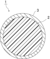
- FIG. 1 is a cross-sectional view schematically showing conductive particles according to the first embodiment of the present invention.
- FIG. 2 is a cross-sectional view schematically showing conductive particles according to a second embodiment of the present invention.
- FIG. 3 is a cross-sectional view schematically showing conductive particles according to a third embodiment of the present invention.
- 4 is a cross-sectional view schematically showing a connection structure using the conductive particles shown in FIG. 1.
- a conductive particle according to the present invention comprises a substrate particle and a conductive portion arranged on the surface of the substrate particle.
- the value of the compression modulus when compressed by 10% is equal to or greater than the value of the compression modulus when compressed by 20%
- the value of the compression modulus when compressed by 20% is It is equal to or greater than the value of compression elastic modulus when compressed by 30%.
- the absolute value of the difference between the compression modulus when compressed by 10% and the compression modulus when compressed by 20%, the compression modulus when compressed by 20% The ratio to value is less than or equal to 0.20.
- the compression modulus at 10% compression, the compression modulus at 20% compression, and the compression modulus at 30% compression are defined as 10% K value, 20% K value, and 30% K value, respectively.
- the conductive particles according to the present invention satisfy the following relationships.
- the "absolute value of the difference between the value of the compression modulus when compressed by 10% and the value of the compression modulus when compressed by 20%" is the ratio (the difference between the 10% K value and the 20% K value). absolute value/20% K value).
- the "absolute value of the difference between the value of the compression modulus when compressed by 10% and the value of the compression modulus when compressed by 20%" is "10% It is a value obtained by subtracting the value of the compression modulus when compressed by 20% from the value of the compression modulus when compressed.
- the conductive particles according to the present invention satisfy the following relationships.
- the absolute value of the difference between the compression modulus when compressed by 10% and the compression modulus when compressed by 20%, the compression modulus when compressed by 20% is small compared to conventional conductive particles. That is, in the conductive particles according to the present invention, the absolute value of the difference between the compression modulus when compressed by 10% and the compression modulus when compressed by 20% is relatively small. Alternatively, the oxide film on the surface of the conductive particles (conductive portion) can be sufficiently removed. As a result, both low connection resistance and high conduction reliability can be achieved when the conductive particles are used for electrical connection between electrodes.
- organic electroluminescence (organic EL) display elements that have good visibility, can be made thin, and can be driven under a low DC voltage.
- Titanium electrodes are often used in organic EL display elements. With conventional conductive particles, it is difficult to sufficiently remove the oxide film on the surface of the titanium electrode. In this case as well, the oxide film on the surface of the electrode can be sufficiently removed, and both low connection resistance and high conduction reliability can be achieved.
- the value of the compression elastic modulus when compressed by 10% is equal to or greater than the value of the compression elastic modulus when compressed by 20%, and the compression elastic modulus when compressed by 20% Since the value is equal to or greater than the value of the compressive elastic modulus when compressed by 30%, the contact area between the electrode and the deformed conductive particles can be increased in the middle and late stages of compression. As a result, both low connection resistance and high conduction reliability can be achieved when the conductive particles are used for electrical connection between electrodes.
- the value of the compression modulus when compressed by 10% and the value of the compression modulus when compressed by 20% may be the same.
- the conductive particles may have the same value of compression modulus when compressed by 20% and the value of compression modulus when compressed by 30%.
- the conductive particles even if the value of the compression modulus when compressed by 10%, the value of the compression modulus when compressed by 20%, and the value of the compression modulus when compressed by 30% are the same good. From the viewpoint of exhibiting the effects of the present invention more effectively, it is preferable that the conductive particles have a compression modulus value when compressed by 10% that is greater than a compression modulus value when compressed by 20%. preferable.
- the conductive particles have a compression modulus value when compressed by 20% greater than a compression modulus value when compressed by 30%.
- the conductive particles have a compression modulus value when compressed by 10% greater than a compression modulus value when compressed by 20%, and , the value of the compression modulus when compressed by 20% is preferably greater than the value of the compression modulus when compressed by 30%.
- the absolute difference between the compression modulus value when compressed by 10% and the compression modulus value when compressed by 20% in the above conductive particles The ratio of the value to the value of compression modulus at 20% compression is preferably less than 0.20, more preferably 0.15 or less, even more preferably 0.13 or less. From the viewpoint of exhibiting the effect of the present invention more effectively, in the conductive particles, the ratio (absolute value of difference between 10% K value and 20% K value/20% K value) is preferably It is more than 0, more preferably 0.05 or more, and still more preferably 0.10 or more.
- the compression elastic modulus value (10% K value) when the conductive particles are compressed by 10% is preferably 10000 N/mm 2 or more, more preferably 12000 N/mm 2 or more, still more preferably 13000 N/mm 2 or more, Particularly preferably, it is 15000 N/mm 2 or more.
- the 10% K value of the conductive particles is preferably 50,000 N/mm 2 or less, more preferably 40,000 N/mm 2 or less, even more preferably 30,000 N/mm 2 or less, and particularly preferably 25,000 N/mm 2 or less.
- the 10% K value of the conductive particles is equal to or less than the upper limit, the contact area between the electrode and the deformed conductive particles can be increased to further reduce the connection resistance.
- the compression elastic modulus value (20% K value) when the conductive particles are compressed by 20% is preferably 10,000 N/mm 2 or more, more preferably 12,000 N/mm 2 or more, and still more preferably 13,000 N/mm 2 or more, Particularly preferably, it is 15000 N/mm 2 or more.
- the 20% K value of the conductive particles is at least the lower limit, the oxide film on the surface of the electrode or the conductive particles (conductive portion) is more effectively eliminated at the initial stage of compression, and the connection resistance is further reduced. be able to.
- the 20% K value of the conductive particles is preferably 40,000 N/mm 2 or less, more preferably 30,000 N/mm 2 or less, still more preferably 25,000 N/mm 2 or less, and particularly preferably 20,000 N/mm 2 or less.
- the 20% K value of the conductive particles is equal to or less than the upper limit, the contact area between the electrode and the deformed conductive particles can be increased to further reduce the connection resistance.
- the compression elastic modulus value (30% K value) when the conductive particles are compressed by 30% is preferably 8,000 N/mm 2 or more, more preferably 10,000 N/mm 2 or more, and still more preferably 12,000 N/mm 2 or more, Particularly preferably, it is 13000 N/mm 2 or more.
- 30% K value of the conductive particles is at least the lower limit, recesses (indentations) in which the conductive particles are pushed into the electrodes are formed in the middle and late stages of compression, and the reliability of conduction between the electrodes is further enhanced. be able to.
- the 30% K value of the conductive particles is preferably 40,000 N/mm 2 or less, more preferably 30,000 N/mm 2 or less, still more preferably 25,000 N/mm 2 or less, and particularly preferably 20,000 N/mm 2 or less.
- the 30% K value of the conductive particles is the above upper limit or less, the contact area between the electrode and the deformed conductive particles is increased in the middle and late compression stages, and both low connection resistance and high conduction reliability are achieved. can be more effectively reconciled.
- the above-described conductive particles have a compressive elastic modulus value (10% K value) when compressed by 20% compared to the value of the elastic modulus when compressed by 10%.
- (20% K value) is preferably 1.00 or more, more preferably 1.05 or more, still more preferably 1.10 or more.
- the ratio (10% K value/20% K value) is preferably 1.20 or less, more preferably less than 1.20, and still more preferably 1 0.15 or less, particularly preferably 1.13 or less.
- the above-described conductive particles have a compression elastic modulus when compressed by 30% compared to the compression elastic modulus value (10% K value) when compressed by 10%.
- (30% K value) is preferably 1.00 or more, more preferably 1.20 or more, still more preferably 1.30 or more.
- the ratio (10% K value/30% K value) is preferably 1.80 or less, more preferably 1.70 or less, and still more preferably 1 0.60 or less, particularly preferably 1.50 or less.
- the above-described conductive particles have a compression elastic modulus when compressed by 30%, which is lower than the compression elastic modulus when compressed by 20% (20% K value).
- (30% K value) is preferably 1.00 or more, more preferably 1.05 or more, still more preferably 1.10 or more.
- the ratio (20% K value/30% K value) is preferably 1.60 or less, more preferably 1.50 or less, and still more preferably 1 0.40 or less, particularly preferably 1.30 or less.
- the 10% K value, 20% K value, and 30% K value of the conductive particles can be measured as follows.
- the conductive particles are compressed at 25°C with a smooth indenter end face of a cylinder (diameter 50 ⁇ m, made of diamond) under the conditions of applying a maximum test load of 90 mN over 30 seconds.
- the load value (N) and compression displacement (mm) at this time are measured. From the obtained measured values, the compression elastic modulus can be obtained by the following formula.
- the microcompression tester for example, "Fischer Scope H-100" manufactured by Fisher Co., Ltd. is used.
- K value (N/mm 2 ) (3/2 1/2 ) F S ⁇ 3/2 R ⁇ 1/2 F: Load value (N) when the conductive particles are compressed by 10%, 20%, or 30% S: Compressive displacement (mm) when the conductive particles are compressed by 10%, 20%, or 30% R: radius of conductive particles (mm)
- a method of controlling the 10% K value, the 20% K value, the 30% K value, and the ratio (the absolute value of the difference between the 10% K value and the 20% K value/20% K value) within a preferable range examples include the following methods.
- the compression recovery rate of the conductive particles is preferably 50% or more, more preferably 60% or more, still more preferably 65% or more, and preferably 95%. Below, more preferably 90% or less, still more preferably 85% or less.
- the compression recovery rate can be measured as follows.
- Scatter conductive particles on the sample stage For one dispersed conductive particle, using a microcompression tester, a cylindrical (diameter 100 ⁇ m, made of diamond) smooth indenter end face, at 25 ° C., 30% of the conductive particle in the center direction of the conductive particle. A load (reverse load value) is applied until compression deformation occurs. After that, unloading is performed to the origin load value (0.40 mN). By measuring the load-compression displacement during this period, the compression recovery rate can be obtained from the following formula. Note that the load speed is 0.33 mN/sec. As the microcompression tester, for example, "Fischer Scope H-100" manufactured by Fisher Co., Ltd. is used.
- Compression recovery rate (%) [L2/L1] x 100
- L1 Compressive displacement from the origin load value to the reverse load value when the load is applied
- L2 Unloading displacement from the reverse load value to the origin load value when releasing the load
- the particle diameter of the conductive particles is preferably 0.5 ⁇ m or more, more preferably 1.0 ⁇ m or more, preferably 500 ⁇ m or less, more preferably 300 ⁇ m or less, still more preferably 100 ⁇ m or less, and particularly preferably 30 ⁇ m or less.
- the particle diameter of the conductive particles is at least the lower limit and at most the upper limit, when the electrodes are connected using the conductive particles, the contact area between the conductive particles and the electrodes is sufficiently large, and the conductive portion It becomes difficult to form agglomerated conductive particles when forming.
- the distance between the electrodes connected via the conductive particles does not become too large, and the conductive portions are less likely to peel off from the surface of the substrate particles.
- the particle size of the conductive particles is equal to or more than the lower limit and equal to or less than the upper limit, the conductive particles can be suitably used as a conductive material.
- the particle size of the conductive particles is preferably an average particle size, more preferably a number average particle size.
- the particle size of the conductive particles can be obtained, for example, by observing 50 arbitrary conductive particles with an electron microscope or an optical microscope and calculating the average particle size of each conductive particle, or by laser diffraction particle size distribution measurement. is obtained by doing In observation with an electron microscope or an optical microscope, the particle size of each conductive particle is obtained as the particle size in circle equivalent diameter. In observation with an electron microscope or an optical microscope, the average particle size of arbitrary 50 conductive particles in equivalent circle diameter is almost equal to the average particle size in equivalent sphere diameter. In the laser diffraction particle size distribution measurement, the particle size of each conductive particle is obtained as the particle size in terms of equivalent sphere diameter.
- the particle size of the conductive particles is preferably calculated by laser diffraction particle size distribution measurement.
- FIG. 1 is a cross-sectional view showing conductive particles according to the first embodiment of the present invention.
- the conductive particles 1 shown in FIG. 1 have base particles 2 and conductive portions 3 .
- the conductive portion 3 is arranged on the surface of the substrate particle 2 .
- the conductive portion 3 is in contact with the surface of the substrate particles 2 .
- the conductive particles 1 are coated particles in which the surfaces of the base particles 2 are coated with the conductive parts 3 .
- the conductive portion 3 is a single-layer conductive portion (conductive layer).
- the conductive particles 1 do not have a core substance, unlike the conductive particles 11 and 21 described later.
- the conductive particles 1 do not have protrusions on their surfaces, and the conductive portions 3 do not have protrusions on their outer surfaces.
- Conductive particles 1 are spherical.
- the conductive particles according to the present invention may have no projections on the surface, may have no projections on the outer surface of the conductive portion, and may be spherical. Also, unlike the conductive particles 11 and 21 to be described later, the conductive particles 1 do not have an insulating substance. However, the conductive particles 1 may have an insulating substance arranged on the outer surface of the conductive portion 3 .
- FIG. 2 is a cross-sectional view showing conductive particles according to the second embodiment of the present invention.
- a conductive particle 11 shown in FIG. 2 has a base particle 2, a conductive portion 12, a plurality of core substances 13, and a plurality of insulating substances 14.
- the conductive portion 12 is arranged on the surface of the substrate particle 2 so as to be in contact with the substrate particle 2 .
- the conductive portion 12 is a single-layer conductive portion (conductive layer).
- the conductive particles 11 have a plurality of protrusions 11a on their surfaces.
- the conductive portion 12 has a plurality of protrusions 12a on its outer surface.
- a plurality of core substances 13 are arranged on the surface of the substrate particles 2 .
- a plurality of core substances 13 are embedded in the conductive portion 12 .
- the core substance 13 is arranged inside the protrusions 11a and 12a.
- the conductive portion 12 covers a plurality of core substances 13 .
- the outer surface of the conductive portion 12 is raised by a plurality of core substances 13 to form projections 11a and 12a.
- the conductive particles 11 have an insulating substance 14 arranged on the outer surface of the conductive portion 12 . At least a partial region of the outer surface of the conductive portion 12 is covered with an insulating material 14 .
- the insulating substance 14 is an insulating particle made of an insulating material.
- the conductive particles according to the present invention may have an insulating material arranged on the outer surface of the conductive portion. However, the conductive particles according to the present invention may not necessarily contain an insulating substance.
- FIG. 3 is a cross-sectional view showing conductive particles according to a third embodiment of the present invention.
- a conductive particle 21 shown in FIG. 3 has a base particle 2 , a conductive portion 22 , multiple core substances 13 , and multiple insulating substances 14 .
- the conductive portion 22 as a whole has a first conductive portion 22A on the substrate particle 2 side and a second conductive portion 22B on the side opposite to the substrate particle 2 side.
- the conductive particles 11 and the conductive particles 21 differ only in the configuration of the conductive portion. That is, in the conductive particles 11, the conductive portion 12 having a single-layer structure is formed, whereas in the conductive particles 21, the first conductive portion 22A and the second conductive portion 22B having a two-layer structure are formed. ing. The first conductive portion 22A and the second conductive portion 22B are formed as separate conductive portions.
- the first conductive portion 22A is arranged on the surface of the substrate particle 2.
- a first conductive portion 22A is arranged between the substrate particle 2 and the second conductive portion 22B.
- the first conductive portion 22A is in contact with the substrate particles 2 . Therefore, the first conductive portion 22A is arranged on the surface of the substrate particle 2, and the second conductive portion 22B is arranged on the surface of the first conductive portion 22A.
- the conductive particles 21 have a plurality of projections 21a on their surfaces.
- the conductive portion 22 has a plurality of protrusions 22a on its outer surface.
- the first conductive portion 22A has projections 22Aa on its outer surface.
- the second conductive portion 22B has a plurality of projections 22Ba on its outer surface.
- the conductive portion 22 is a two-layered conductive portion (conductive layer).
- (meth)acrylic means one or both of “acrylic” and “methacrylic”
- (meth)acrylate means one or both of “acrylate” and “methacrylate”.
- the substrate particles include resin particles, inorganic particles other than metal particles, organic-inorganic hybrid particles, and metal particles.
- the substrate particles may be core-shell particles comprising a core and a shell arranged on the surface of the core.
- the core may be an organic core.
- the shell may be an inorganic shell.
- the substrate particles are preferably resin particles or organic-inorganic hybrid particles, and more preferably organic-inorganic hybrid particles, because the effects of the present invention are more excellent.
- the base particles are preferably resin particles made of resin.
- the conductive particles are placed between the electrodes and then pressed to compress the conductive particles.
- the substrate particles are resin particles, the conductive particles are easily deformed during the pressure bonding, and the contact area between the conductive particles and the electrode increases. Therefore, the reliability of electrical connection between the electrodes is further enhanced.
- the resin that is the material of the resin particles include polyolefin resins such as polyethylene, polypropylene, polystyrene, polyvinyl chloride, polyvinylidene chloride, polyisobutylene, and polybutadiene; acrylic resins such as polymethyl methacrylate and polymethyl acrylate; Terephthalate, polycarbonate, polyamide, phenol formaldehyde resin, melamine formaldehyde resin, benzoguanamine formaldehyde resin, urea formaldehyde resin, phenol resin, melamine resin, benzoguanamine resin, urea resin, epoxy resin, unsaturated polyester resin, saturated polyester resin, polysulfone, polyphenylene oxide , polyacetal, polyimide, polyamideimide, polyetheretherketone, polyethersulfone, and polymers obtained by polymerizing one or more of various polymerizable monomers having an ethacrylate, polyethylene, polypropylene, polystyrene, polyviny
- the resin for forming the resin particles is obtained by polymerizing one or more polymerizable monomers having a plurality of ethylenically unsaturated groups. Polymers are preferred.
- the polymerizable monomer having an ethylenically unsaturated group includes a non-crosslinkable monomer and a crosslinkable monomer. and a monomer of
- non-crosslinkable monomers examples include styrene-based monomers such as styrene and ⁇ -methylstyrene; carboxyl group-containing monomers such as (meth)acrylic acid, maleic acid and maleic anhydride; meth)acrylate, ethyl (meth)acrylate, propyl (meth)acrylate, butyl (meth)acrylate, 2-ethylhexyl (meth)acrylate, lauryl (meth)acrylate, cetyl (meth)acrylate, stearyl (meth)acrylate, cyclohexyl ( Alkyl (meth)acrylate compounds such as meth)acrylate and isobornyl (meth)acrylate; Oxygen atoms such as 2-hydroxyethyl (meth)acrylate, glycerol (meth)acrylate, polyoxyethylene (meth)acrylate, and glycidyl (meth)acrylate Containing (meth)
- crosslinkable monomer examples include tetramethylolmethane tetra(meth)acrylate, tetramethylolmethane tri(meth)acrylate, tetramethylolmethane di(meth)acrylate, trimethylolpropane tri(meth)acrylate, dipenta Erythritol hexa(meth)acrylate, dipentaerythritol penta(meth)acrylate, glycerol tri(meth)acrylate, glycerol di(meth)acrylate, (poly)ethylene glycol di(meth)acrylate, (poly)propylene glycol di(meth)acrylate Polyfunctional (meth)acrylate compounds such as acrylate, (poly)tetramethylene glycol di(meth)acrylate, 1,4-butanediol di(meth)acrylate; triallyl (iso)cyanurate, triallyl trimellitate, divinylbenzene,
- the resin particles can be obtained by polymerizing the polymerizable monomer having the ethylenically unsaturated group by a known method. Examples of this method include a method of suspension polymerization in the presence of a radical polymerization initiator, and a method of polymerizing by swelling a monomer together with a radical polymerization initiator using uncrosslinked seed particles.
- the substrate particles are inorganic particles excluding metal particles or organic-inorganic hybrid particles
- examples of inorganic substances that are materials of the substrate particles include silica and carbon black.
- the inorganic substance is not a metal.
- the particles formed of silica are not particularly limited, but for example, after hydrolyzing a silicon compound having two or more hydrolyzable alkoxysilyl groups to form crosslinked polymer particles, firing is performed as necessary. Particles obtained by carrying out.
- the organic-inorganic hybrid particles include organic-inorganic hybrid particles formed from a crosslinked alkoxysilyl polymer and an acrylic resin.
- the substrate particles are metal particles
- examples of metals that are materials of the metal particles include silver, copper, nickel, silicon, gold, and titanium.
- the substrate particles are preferably not metal particles, and preferably not copper particles.
- the compression elastic modulus value (10% K value) when the base particles are compressed by 10% is preferably 9500 N/mm 2 or more, more preferably 10500 N/mm 2 or more, still more preferably 13500 N/mm 2 or more, Particularly preferably, it is 16500 N/mm 2 or more.
- the 10% K value of the substrate particles is preferably 31,500 N/mm 2 or less, more preferably 30,500 N/mm 2 or less, still more preferably 27,500 N/mm 2 or less, and particularly preferably 24,500 N/mm 2 or less.
- the 10% K value of the substrate particles is equal to or less than the upper limit, the contact area between the electrode and the deformed conductive particles can be increased, and the connection resistance can be further reduced.
- the compression elastic modulus value (20% K value) when the base particles are compressed by 20% is preferably 9000 N/mm 2 or more, more preferably 10000 N/mm 2 or more, still more preferably 13000 N/mm 2 or more, Particularly preferably, it is 16000 N/mm 2 or more.
- the 20% K value of the base particles is at least the lower limit, the oxide film on the surface of the electrode or the conductive particles (conductive portion) is more effectively eliminated at the initial stage of compression, and the connection resistance is further reduced. be able to.
- the 20% K value of the substrate particles is preferably 31,000 N/mm 2 or less, more preferably 30,000 N/mm 2 or less, even more preferably 27,000 N/mm 2 or less, and particularly preferably 24,000 N/mm 2 or less.
- the 20% K value of the substrate particles is equal to or less than the upper limit, the contact area between the electrode and the deformed conductive particles can be increased, and the connection resistance can be further reduced.
- the compression elastic modulus value (30% K value) when the base particles are compressed by 30% is preferably 8000 N/mm 2 or more, more preferably 9000 N/mm 2 or more, and still more preferably 12000 N/mm 2 or more. Particularly preferably, it is 15000 N/mm 2 or more.
- 30% K value of the base particles is at least the lower limit, recesses (indentations) in which the conductive particles are pushed into the electrodes are formed in the middle and late stages of compression, and the reliability of conduction between the electrodes is further enhanced. be able to.
- the 30% K value of the substrate particles is preferably 30,000 N/mm 2 or less, more preferably 29,000 N/mm 2 or less, still more preferably 27,000 N/mm 2 or less, and particularly preferably 24,000 N/mm 2 or less.
- the 30% K value of the base particles is equal to or less than the upper limit, the contact area between the electrode and the deformed conductive particles is increased in the middle and late stages of compression, and both low connection resistance and high conduction reliability are achieved. can be more effectively reconciled.
- the particle diameter of the substrate particles is preferably 0.1 ⁇ m or more, more preferably 1.0 ⁇ m or more, still more preferably 1.5 ⁇ m or more, and particularly preferably 2.0 ⁇ m or more.
- the particle size of the substrate particles is preferably 500 ⁇ m or less, more preferably 300 ⁇ m or less, still more preferably 50 ⁇ m or less, still more preferably 30 ⁇ m or less, particularly preferably 10 ⁇ m or less, and most preferably 5.0 ⁇ m or less.
- the conductive portion is formed on the surface of the base material particles by electroless plating, it becomes difficult to form agglomerated conductive particles.
- the particle size of the substrate particles is equal to or less than the upper limit, the conductive particles are sufficiently compressed, the connection resistance between the electrodes becomes even lower, and the distance between the electrodes becomes smaller.
- the particle size of the base material particles indicates the number average particle size.
- the particle size of the substrate particles is determined using a particle size distribution analyzer or the like.
- the particle diameter of the substrate particles is preferably determined by observing 50 arbitrary substrate particles with an electron microscope or an optical microscope and calculating the average value. In observation with an electron microscope or an optical microscope, the particle size of each base particle is obtained as the particle size of the equivalent circle diameter. In observation with an electron microscope or an optical microscope, the average particle size of arbitrary 50 substrate particles in the equivalent circle diameter is approximately equal to the average particle size in the equivalent sphere diameter.
- the particle size of one base particle is determined as the particle size in terms of equivalent sphere diameter. It is preferable to calculate the particle size of the substrate particles using a particle size distribution analyzer. When measuring the particle size of the substrate particles of the conductive particles, it can be measured, for example, as follows.
- a metal for forming the conductive portion is not particularly limited.
- the above metals include gold, silver, palladium, copper, platinum, zinc, iron, tin, lead, ruthenium, aluminum, cobalt, indium, nickel, chromium, titanium, antimony, bismuth, thallium, germanium, cadmium, and silicon. and alloys thereof.
- the metal include tin-doped indium oxide (ITO) and solder.
- ITO tin-doped indium oxide
- An alloy containing tin, nickel, palladium, copper or gold is preferable, and nickel or palladium is preferable, since the connection resistance between the electrodes can be further lowered.
- the conductive portion may be formed of one layer.
- the conductive portion may be formed of multiple layers. That is, the conductive portion may have a laminated structure of two or more layers.
- the outermost layer is preferably a gold layer, a nickel layer, a palladium layer, a ruthenium layer, a copper layer, or an alloy layer containing tin and silver. more preferably a layer, a palladium layer or a ruthenium layer.
- the outermost layer is one of these preferred conductive layers, the connection resistance between the electrodes is even lower.
- the outermost layer is a noble metal layer, the corrosion resistance is further enhanced.
- the method of forming the conductive portion on the surface of the substrate particles is not particularly limited.
- Methods for forming the conductive portion include, for example, a method by electroless plating, a method by electroplating, a method by physical vapor deposition, and a method of coating the surface of the substrate particles with a metal powder or a paste containing a metal powder and a binder. etc.
- a method using electroless plating is preferable because the formation of the conductive portion is simple.
- Methods such as vacuum deposition, ion plating, and ion sputtering can be used as the method by physical vapor deposition.
- the thickness of the conductive portion is preferably 10 nm or more, more preferably 100 nm or more, still more preferably 120 nm or more, preferably 1000 nm or less, more preferably 500 nm or less, still more preferably 300 nm or less, It is particularly preferably 250 nm or less, most preferably 200 nm or less.
- the thickness of the conductive portion is the thickness of the entire conductive layer when the conductive portion has multiple layers. When the thickness of the conductive portion is at least the above lower limit and at most the above upper limit, sufficient conductivity is obtained, and the conductive particles are sufficiently deformed when connecting the electrodes without becoming too hard. .
- the thickness of the outermost conductive layer is preferably 1 nm or more, more preferably 10 nm or more, and preferably 500 nm or less, more preferably 200 nm or less.
- the thickness of the outermost conductive layer is equal to or more than the lower limit and equal to or less than the upper limit, the coating with the outermost conductive layer is uniform, the corrosion resistance is sufficiently high, and the connection resistance between electrodes is further increased. lower.
- the outermost layer is a gold layer, the thinner the gold layer, the lower the cost.
- the thickness of the conductive portion can be measured by observing the cross section of the conductive particles using, for example, a transmission electron microscope (TEM).
- TEM transmission electron microscope
- the conductive particles preferably have a conductive portion containing nickel.
- the nickel content is preferably 50% by weight or more, more preferably 65% by weight or more, even more preferably 70% by weight or more, still more preferably 75% by weight or more, and even more preferably is at least 80% by weight, particularly preferably at least 85% by weight, most preferably at least 90% by weight.
- the nickel content is preferably 100% by weight (total amount) or less, may be 99% by weight or less, or may be 95% by weight or less. If the nickel content is at least the above lower limit, the connection resistance between the electrodes will be even lower. In addition, when the oxide film on the surface of the electrode or the conductive portion is small, the connection resistance between the electrodes tends to decrease as the nickel content increases.
- Various known analysis methods can be used for measuring the content of the metal contained in the conductive portion, and there is no particular limitation.
- this measuring method include absorption spectrometry, spectral analysis, and the like.
- absorption analysis method a flame absorption photometer, an electric heating furnace absorption photometer, or the like can be used.
- spectral analysis methods include plasma emission spectrometry and plasma ion source mass spectrometry.
- ICP emission spectrometer When measuring the average content of the metal contained in the conductive portion, it is preferable to use an ICP emission spectrometer.
- ICP emission spectrometers include ICP emission spectrometers manufactured by HORIBA.
- the conductive portion may contain phosphorus or boron in addition to nickel. Also, the conductive portion may contain a metal other than nickel. When the conductive portion contains a plurality of metals, the plurality of metals may be alloyed.
- the content of phosphorus or boron is preferably 0.1% by weight or more, more preferably 0.5% by weight or more, and preferably 10% by weight or less, More preferably, it is 5% by weight or less.
- the content of phosphorus or boron is equal to or less than the lower limit and the upper limit, the connection resistance of the conductive portion is further lowered, and the conductive portion contributes to the reduction of the connection resistance.
- the conductive particles have a plurality of projections on the outer surface of the conductive portion. Furthermore, it is preferable that the conductive particles include a plurality of core substances protruding from the outer surface of the conductive portion so as to form a plurality of protrusions within the conductive portion.
- the conductive portion By embedding the core material in the conductive portion, the conductive portion can easily have a plurality of projections on the outer surface.
- the core substance may not necessarily be used to form projections on the surface of the conductive particles and the surface of the conductive portion.
- a method of forming a conductive portion by electroless plating after attaching a core substance to the surface of the substrate particle As a method of forming the protrusions, a method of forming a conductive portion by electroless plating after attaching a core substance to the surface of the substrate particle, and a method of forming a conductive portion by electroless plating on the surface of the substrate particle. , a method of adhering a core substance and then forming a conductive portion by electroless plating, and a method of adding a core substance in the middle of forming a conductive portion on the surface of a substrate particle by electroless plating.
- Materials for the core substance include conductive substances and non-conductive substances.
- the conductive substance include metals, metal oxides, conductive nonmetals such as graphite, and conductive polymers. Polyacetylene etc. are mentioned as said conductive polymer.
- the non-conductive substance include silica, alumina, tungsten carbide, titanium oxide, barium titanate, and zirconia.
- the metal that is the material of the core substance the metals listed as the material of the conductive material can be appropriately used.
- materials for the core substance include barium titanate (Mohs hardness 4.5), nickel (Mohs hardness 5), silica (silicon dioxide, Mohs hardness 6 to 7), titanium oxide (Mohs hardness 7), and zirconia. (Mohs hardness 8 to 9), alumina (Mohs hardness 9), tungsten carbide (Mohs hardness 9) and diamond (Mohs hardness 10).
- the inorganic particles are preferably nickel, silica, titanium oxide, zirconia, alumina, tungsten carbide or diamond, more preferably silica, titanium oxide, zirconia, alumina, tungsten carbide or diamond.
- the inorganic particles are more preferably titanium oxide, zirconia, alumina, tungsten carbide or diamond, and particularly preferably zirconia, alumina, tungsten carbide or diamond.
- the Mohs hardness of the material of the core substance is preferably 4 or higher, more preferably 6 or higher, even more preferably 7 or higher, and particularly preferably 7.5 or higher.
- the Mohs hardness of the material of the core substance is at least the lower limit, the 10% K value, the 20% K value, the 30% K value, and the ratio (the difference between the 10% K value and the 20% K value (absolute value of /20% K value) can be easily controlled within a suitable range.
- the shape of the core substance is not particularly limited.
- the shape of the core substance is preferably massive.
- the core substance includes, for example, particulate lumps, agglomerates in which a plurality of microparticles are aggregated, and amorphous lumps.
- the average particle size of the core substance is preferably 0.001 ⁇ m or more, more preferably 0.05 ⁇ m or more, and preferably 0.9 ⁇ m or less, more preferably 0.2 ⁇ m or less.
- the connection resistance between electrodes is effectively lowered.
- the average particle size of the core substance is preferably the number average particle size.
- the average particle size of the core substance is obtained by observing 50 arbitrary core substances with an electron microscope or an optical microscope and calculating the average value.
- the number of protrusions per conductive particle is preferably 3 or more, more preferably 5 or more.
- the upper limit of the number of protrusions is not particularly limited. The upper limit of the number of protrusions can be appropriately selected in consideration of the particle size of the conductive particles.
- the surface area of the portion having the protrusions is preferably 10% or more, more preferably 30% or more, out of 100% of the total surface area of the conductive particles. , preferably 95% or less, more preferably 90% or less.
- the average height of the plurality of projections is preferably 0.001 ⁇ m or more, more preferably 0.05 ⁇ m or more, and preferably 0.9 ⁇ m or less, more preferably 0.5 ⁇ m or less.
- the connection resistance between the electrodes is effectively lowered.
- the conductive particles comprise an insulating material disposed on the surface of the conductive portion.
- the conductive particles are used to connect the electrodes, it is possible to further prevent short circuits between the adjacent electrodes.
- an insulating material exists between the plurality of electrodes, so short-circuiting between laterally adjacent electrodes can be prevented instead of between the electrodes above and below.
- the electrodes are connected, the insulating material between the conductive portion of the conductive particles and the electrodes can be easily eliminated by pressing the conductive particles with two electrodes.
- the conductive particles have a plurality of protrusions on the outer surface of the conductive portion, the insulating material between the conductive portion of the conductive particles and the electrode can be removed more easily.
- the insulating substance is preferably insulating particles because the insulating substance can be more easily removed when the electrodes are crimped.
- the particle size of the insulating material can be appropriately selected depending on the particle size of the conductive particles, the application of the conductive particles, and the like. In addition, from the viewpoint of improving insulation performance, insulating substances having different particle sizes may be mixed and used.
- the particle size of the insulating substance is preferably 0.005 ⁇ m or more, more preferably 0.01 ⁇ m or more, and preferably 1 ⁇ m or less, more preferably 0.5 ⁇ m or less. If the particle diameter of the insulating substance is equal to or greater than the lower limit, the conductive portions of the plurality of conductive particles are less likely to come into contact with each other when the conductive particles are dispersed in the binder resin. When the particle diameter of the insulating particles is equal to or less than the upper limit, there is no need to apply an excessively high pressure to remove the insulating substance between the electrodes and the conductive particles when connecting the electrodes. No need to heat to high temperatures.
- the conductive material according to the present invention contains the conductive particles described above and a binder resin.
- the conductive particles are preferably dispersed in a binder resin and used as a conductive material.
- the conductive material is preferably an anisotropic conductive material.
- the conductive particles and the conductive material are each used for electrical connection between electrodes.
- Each of the conductive particles and the conductive material is suitably used for electrical connection between electrodes of an organic EL display element.
- the conductive material is preferably a circuit connecting material.
- the binder resin is not particularly limited.
- the binder resin preferably contains a thermoplastic component (thermoplastic compound) or a curable component, and more preferably contains a curable component.
- the curable component include photocurable components and thermosetting components.
- the photocurable component preferably contains a photocurable compound and a photopolymerization initiator.
- the thermosetting component preferably contains a thermosetting compound and a thermosetting agent.
- the binder resin include vinyl resins, thermoplastic resins, curable resins, thermoplastic block copolymers and elastomers. Only one type of the binder resin may be used, or two or more types may be used in combination.
- Examples of the vinyl resin include vinyl acetate resin, acrylic resin and styrene resin.
- examples of the thermoplastic resins include polyolefin resins, ethylene-vinyl acetate copolymers and polyamide resins.
- examples of the curable resin include epoxy resin, urethane resin, polyimide resin and unsaturated polyester resin.
- the curable resin may be a room temperature curable resin, a thermosetting resin, a photocurable resin, or a moisture curable resin.
- thermoplastic block copolymers examples include styrene-butadiene-styrene block copolymers, styrene-isoprene-styrene block copolymers, hydrogenated products of styrene-butadiene-styrene block copolymers, and styrene-isoprene. - hydrogenated products of styrene block copolymers;
- the elastomer examples include styrene-butadiene copolymer rubber and acrylonitrile-styrene block copolymer rubber.
- the conductive material and the binder resin preferably contain a thermoplastic component or a thermosetting component.
- the conductive material and the binder resin may contain a thermoplastic component or may contain a thermosetting component.
- the conductive material and the binder resin preferably contain a thermosetting component.
- the thermosetting component preferably contains a curable compound that can be cured by heating and a thermosetting agent.
- the heat curing agent is preferably a heat cationic curing initiator.
- the curable compound that can be cured by heating and the thermosetting agent are used in an appropriate compounding ratio so that the binder resin is cured.
- the binder resin contains a thermal cationic curing initiator, the cured product tends to contain an acid.
- the connection resistance between the electrodes can be kept low.
- Examples of the conductive material include fillers, extenders, softeners, plasticizers, polymerization catalysts, curing catalysts, colorants, antioxidants, heat stabilizers, light stabilizers, ultraviolet absorbers, lubricants, antistatic agents and Various additives such as flame retardants may be included.
- the conductive material can be used as a conductive paste, a conductive film, and the like.
- the conductive material is a conductive film
- a film containing no conductive particles may be laminated on the conductive film containing conductive particles.
- the conductive paste is preferably an anisotropic conductive paste.
- the conductive film is preferably an anisotropic conductive film.
- the content of the binder resin is preferably 10% by weight or more, more preferably 30% by weight or more, still more preferably 50% by weight or more, and particularly preferably 70% by weight or more. 99.99% by weight or less, more preferably 99.9% by weight or less.
- the content of the binder resin is at least the lower limit and at most the upper limit, the conductive particles are efficiently arranged between the electrodes, and the conduction reliability of the connection target member connected by the conductive material is further increased.
- the content of the conductive particles in 100% by weight of the conductive material is preferably 0.01% by weight or more, more preferably 0.1% by weight or more, and preferably 80% by weight or less, more preferably 60% by weight. 40% by weight or less, particularly preferably 20% by weight or less, and most preferably 10% by weight or less.
- content of the conductive particles is equal to or more than the lower limit and equal to or less than the upper limit, reliability of electrical connection between electrodes is further enhanced.
- connection structure A connected structure can be obtained by connecting members to be connected using the conductive particles or a conductive material containing the conductive particles and a binder resin.
- connection structure connects a first member to be connected having a first electrode on its surface, a second member to be connected having a second electrode on its surface, and the first and second members to be connected. a connecting portion, wherein the material of the connecting portion comprises the conductive particles described above. In the connection structure, the first electrode and the second electrode are connected by the conductive particles.
- FIG. 4 is a front cross-sectional view schematically showing a connection structure using conductive particles according to the first embodiment of the present invention.
- a connection structure 51 shown in FIG. 4 includes a first connection target member 52, a second connection target member 53, and a connection portion 54 connecting the first and second connection target members 52 and 53.
- the connecting portion 54 is formed by curing a conductive material containing the conductive particles 1 .
- the conductive particles 1 are schematically shown for convenience of illustration. Instead of the conductive particles 1, conductive particles 11, 21, etc. may be used.
- the first connection object member 52 has a plurality of first electrodes 52a on its surface (upper surface).
- the second connection target member 53 has a plurality of second electrodes 53a on its surface (lower surface).
- a first electrode 52 a and a second electrode 53 a are electrically connected by one or more conductive particles 1 . Therefore, the first and second connection object members 52 and 53 are electrically connected by the conductive particles 1 .
- the manufacturing method of the connection structure is not particularly limited.
- the conductive material is arranged between the first member to be connected and the second member to be connected to obtain a laminate, and then the laminate is heated. and a method of pressurizing.
- the pressurization pressure is about 1.0 ⁇ 10 6 Pa to 4.9 ⁇ 10 8 Pa per total area of the connection portion of the electrodes.
- the heating temperature is about 120.degree. C. to 220.degree.
- the total area of the connection portion of the electrode is not limited to the area of the portion in contact with the conductive particles, and in a plan view (in the stacking direction of the first connection target member, the connection portion, and the second connection target member) sometimes) means the total area of the facing portions of the two electrodes.
- the members to be connected include electronic parts such as semiconductor chips, capacitors and diodes, and electronic parts such as circuit boards such as printed boards, flexible printed boards, glass epoxy boards and glass boards.
- the member to be connected is preferably an electronic component.
- the conductive particles are preferably used for electrical connection of electrodes in electronic components.
- At least one of the first member to be connected and the second member to be connected is preferably a flexible printed circuit board. At least one of the first member to be connected and the second member to be connected is preferably a semiconductor chip. The first member to be connected and the second member to be connected are preferably a flexible printed circuit board and a semiconductor chip.
- the material of the flexible printed circuit board is preferably polyimide or polyester, and in the case of polyester, it is preferably polyethylene terephthalate (PET).
- PET polyethylene terephthalate
- the conductive particles and the conductive material are suitably used for conducting a flexible printed circuit board.
- the electrodes provided on the connection target members include metal electrodes such as gold electrodes, nickel electrodes, tin electrodes, aluminum electrodes, copper electrodes, silver electrodes, titanium electrodes, molybdenum electrodes and tungsten electrodes.
- the electrode is preferably a gold electrode, a nickel electrode, a titanium electrode, a tin electrode, or a copper electrode.
- the electrode is preferably an aluminum electrode, a titanium electrode, a copper electrode, a molybdenum electrode, or a tungsten electrode.
- the electrode When the electrode is an aluminum electrode, it may be an electrode made of only aluminum, or an electrode in which an aluminum layer is laminated on the surface of a metal oxide layer.
- materials for the metal oxide layer include indium oxide doped with a trivalent metal element and zinc oxide doped with a trivalent metal element.
- the trivalent metal elements include Sn, Al and Ga.
- the conductive particles according to the present invention are preferably conductive particles for conductive connection of titanium electrodes.
- the conductive particles according to the present invention may be used for conductive connection between titanium electrodes, or may be used for conductive connection between titanium electrodes and electrodes other than titanium electrodes.
- a titanium electrode is an electrode containing titanium.
- Substrate particles A resin particles (divinylbenzene copolymer resin particles, "Micropearl SP-203" manufactured by Sekisui Chemical Co., Ltd., average particle size 3.0 ⁇ m)
- Substrate particles B organic-inorganic hybrid particles (prepared according to Synthesis Example 1 below, average particle size 3.0 ⁇ m)
- Substrate particles C organic-inorganic hybrid particles (different from substrate particles B only in particle diameter, average particle diameter 2.5 ⁇ m)
- Base particle D organic-inorganic hybrid particles (different from base particle B only in particle size, average particle size 10 ⁇ m)
- Example 1 A dispersion liquid was obtained by adding the substrate particles B to 500 parts by weight of distilled water and dispersing them.
- a nickel plating solution (pH 8.5) containing 0.35 mol/L nickel sulfate, 1.38 mol/L dimethylamine borane, and 0.5 mol/L sodium citrate was also prepared. While stirring the resulting suspension at 60° C., the nickel plating solution was gradually dropped into the suspension to perform electroless nickel plating. After that, by filtering the suspension, the particles are taken out, washed with water, and dried to arrange a nickel-boron conductive layer (thickness 142 nm) on the surface of the base particle B, and the surface is a conductive layer. Conductive particles were obtained.
- the nickel plating solution is a mixture of nickel sulfate 200 g / L, sodium hypophosphite 85 g / L, sodium citrate 30 g / L, thallium nitrate 50 ppm, and bismuth nitrate 20 ppm.
- Conductive particles were obtained in the same manner as in Example 1, except that the plating solution was changed to an alloy plating solution and the thickness of the conductive portion was changed.
- the nickel plating solution is a pure nickel plating solution obtained by adjusting the pH of a mixed solution containing 200 g/L of nickel sulfate, 50 g/L of hydrazine hydrate, 30 g/L of sodium citrate, 50 ppm of thallium nitrate, and 20 ppm of bismuth nitrate to pH 6.5.
- Conductive particles were obtained in the same manner as in Example 1, except that the thickness of the conductive portion was changed.
- Example 4 The substrate particles B were added to 100 parts by weight of a 1% by weight solution of dimethylamine borane to activate the surfaces of the substrate particles B. After sufficiently washing the surface-activated substrate particles B with water, they were added to 500 parts by weight of distilled water and dispersed to obtain a dispersion liquid. Next, 1 g of nickel particle slurry (average particle size: 150 nm) was added to the dispersion liquid over 3 minutes to obtain a suspension containing base particles B to which the core substance was attached. A nickel plating solution (pH 8.5) containing 0.35 mol/L nickel sulfate, 1.38 mol/L dimethylamine borane, and 0.5 mol/L sodium citrate was also prepared.
- the nickel plating solution was gradually dropped into the suspension to perform electroless nickel plating. After that, by filtering the suspension, the particles are taken out, washed with water, and dried to arrange a nickel-boron conductive layer (thickness 158 nm) on the surface of the base particle B, and the surface is a conductive layer. Conductive particles were obtained. Out of 100% of the total surface area of the outer surface of the conductive portion, the surface area of the portion having the protrusions was 70%.
- Example 5 Conductive particles were obtained in the same manner as in Example 4, except that the nickel particle slurry was changed to alumina particle slurry (average particle size: 150 nm) and the thickness of the conductive portion was changed.
- Example 6 Conductive particles were obtained in the same manner as in Example 4, except that the nickel particle slurry was changed to titanium oxide particle slurry (average particle size: 150 nm) and the thickness of the conductive portion was changed.
- Example 7 Same as Example 1, except that no particle slurry was used to form the protrusions, and the protrusions were formed by adjusting the amount of precipitation to partially change when forming the conductive portion, and the thickness of the conductive portion was changed. to obtain conductive particles.
- Example 8 In the same manner as in Example 4, except that a palladium plating layer (thickness 20 nm) was formed on the outer surface of the nickel-boron conductive layer when producing the conductive particles, and the thickness of the conductive portion was changed. , to obtain conductive particles.
- Example 9 In the same manner as in Example 4, except that a gold plating layer (thickness 20 nm) was formed on the outer surface of the nickel-boron conductive layer when producing the conductive particles, and the thickness of the conductive portion was changed. , to obtain conductive particles.
- a gold plating layer thickness 20 nm
- Example 10 A conductive particle was obtained in the same manner as in Example 1, except that the base particle B was changed to the base particle A and the thickness of the conductive portion was changed.
- Example 11 A conductive particle was obtained in the same manner as in Example 2, except that the base particle B was changed to the base particle A and the thickness of the conductive portion was changed.
- Example 12 A conductive particle was obtained in the same manner as in Example 4, except that the base particle B was changed to the base particle C and the thickness of the conductive portion was changed.
- Example 13 Conductive particles were obtained in the same manner as in Example 4, except that substrate particles B were changed to substrate particles D and the thickness of the conductive portion was changed.
- Example 14 Prepare a monomer composition containing 100 mmol of methyl methacrylate, 1 mmol of N,N,N-trimethyl-N-2-methacryloyloxyethylammonium chloride, and 1 mmol of 2,2′-azobis(2-amidinopropane) dihydrochloride bottom.
- the above monomer composition was added to deionized water so that the solid content was 5% by weight. Weighed. Then, the mixture was stirred at 200 rpm and polymerized at 70° C. for 24 hours under a nitrogen atmosphere. After completion of the reaction, the mixture was lyophilized to obtain insulating particles having an ammonium group on the surface, an average particle size of 220 nm and a CV value of 10%.
- the insulating particles were dispersed in ion-exchanged water under ultrasonic irradiation to obtain a 10% by weight aqueous dispersion of insulating particles.
- Example 4 10 g of the conductive particles obtained in Example 4 were dispersed in 500 mL of ion-exchanged water, 4 g of an aqueous dispersion of insulating particles was added, and the mixture was stirred at room temperature for 6 hours. After filtration through a 3 ⁇ m mesh filter, the particles were further washed with methanol and dried to obtain conductive particles to which insulating particles adhered.
- Example 15 In the same manner as in Example 4, except that a ruthenium plating layer (thickness of 20 nm) was formed on the outer surface of the nickel-boron conductive layer when producing the conductive particles, and that the thickness of the conductive portion was changed. , to obtain conductive particles.
- a ruthenium plating layer thickness of 20 nm
- Example 1 A conductive particle was obtained in the same manner as in Example 1, except that the base particle B was changed to the base particle A and the thickness of the conductive portion was changed.
- Example 2 A conductive particle was obtained in the same manner as in Example 4, except that the base particle B was changed to the base particle A and the thickness of the conductive portion was changed.
- Example 3 A conductive particle was obtained in the same manner as in Example 14, except that the base particle B was changed to the base particle A and the thickness of the conductive portion was changed.
- Example 4 A conductive particle was obtained in the same manner as in Example 14, except that the base particle B was changed to the base particle A and the thickness of the conductive portion was changed.
- Compression modulus of conductive particles (10% K value, 20% K value, and 30% K value) and ratio (absolute value of difference between 10% K value and 20% K value/20% K value )
- the compression elastic modulus (10% K value, 20% K value, and 30% K value) of the obtained conductive particles was measured using a microcompression tester ("Fisherscope H-100" manufactured by Fisher Co., Ltd.) by the method described above. ) was used.
- the ratio of the absolute value of the difference between the value of the compression modulus when compressed by 10% and the value of the compression modulus when compressed by 20% to the value of the compression modulus when compressed by 20% (10% K
- the absolute value of the difference between the value and the 20% K value/20% K value was calculated.
- An anisotropic conductive paste was prepared by adding the obtained conductive particles to "Structbond XN-5A" manufactured by Mitsui Chemicals Co., Ltd. so that the content was 10% by weight and dispersed. .
- a polyimide substrate (flexible printed substrate) having a Ti--Al--Ti multilayer electrode pattern with L/S of 20 ⁇ m/20 ⁇ m on its upper surface was prepared.
- a semiconductor chip having a gold electrode pattern with L/S of 20 ⁇ m/20 ⁇ m on the lower surface was prepared.
- the anisotropic conductive paste immediately after production was applied onto the polyimide substrate so as to have a thickness of 30 ⁇ m to form an anisotropic conductive paste layer.
- the semiconductor chip was laminated on the anisotropic conductive paste layer so that the electrodes faced each other.
- a pressure heating head is placed on the upper surface of the semiconductor chip, and a pressure of 40 MPa per total bump area is applied to anisotropically.
- the conductive paste layer was cured at 150° C. to obtain a connection structure.
- a connection resistance A between opposing electrodes of the obtained connection structure was measured by a four-probe method. The connection resistance was judged according to the following criteria.
- connection resistance A is 2.0 ⁇ or less ⁇ : Connection resistance A is over 2.0 ⁇ and is 3.0 ⁇ or less ⁇ : Connection resistance A is over 3.0 ⁇ and is 5.0 ⁇ or less ⁇ : Connection resistance A exceeds 5.0 ⁇
- connection structure after the connection resistance evaluation (2) was left under conditions of 85° C. and 85% humidity for 500 hours.
- the connection resistance B between the upper and lower electrodes of the connection structure after being left for 500 hours was measured by the four-probe method. From the connection resistances A and B, the conduction reliability after being left at high temperature and high humidity was determined according to the following criteria.
- connection resistance B is less than 1.25 times the connection resistance A ⁇ : The connection resistance B is 1.25 times or more and less than 1.5 times the connection resistance A ⁇ : The connection resistance B is 1 of the connection resistance A .5 times or more and less than 2.0 times ⁇ : Connection resistance B is 2.0 times or more of connection resistance A
Landscapes
- Physics & Mathematics (AREA)
- Chemical & Material Sciences (AREA)
- Dispersion Chemistry (AREA)
- Spectroscopy & Molecular Physics (AREA)
- Conductive Materials (AREA)
Priority Applications (3)
| Application Number | Priority Date | Filing Date | Title |
|---|---|---|---|
| JP2023515852A JPWO2023145664A1 (https=) | 2022-01-27 | 2023-01-23 | |
| KR1020247018697A KR20240142404A (ko) | 2022-01-27 | 2023-01-23 | 도전성 입자, 도전 재료 및 접속 구조체 |
| CN202380015244.4A CN118402017A (zh) | 2022-01-27 | 2023-01-23 | 导电性粒子、导电材料和连接结构体 |
Applications Claiming Priority (2)
| Application Number | Priority Date | Filing Date | Title |
|---|---|---|---|
| JP2022011158 | 2022-01-27 | ||
| JP2022-011158 | 2022-01-27 |
Publications (1)
| Publication Number | Publication Date |
|---|---|
| WO2023145664A1 true WO2023145664A1 (ja) | 2023-08-03 |
Family
ID=87471930
Family Applications (1)
| Application Number | Title | Priority Date | Filing Date |
|---|---|---|---|
| PCT/JP2023/001815 Ceased WO2023145664A1 (ja) | 2022-01-27 | 2023-01-23 | 導電性粒子、導電材料及び接続構造体 |
Country Status (4)
| Country | Link |
|---|---|
| JP (1) | JPWO2023145664A1 (https=) |
| KR (1) | KR20240142404A (https=) |
| CN (1) | CN118402017A (https=) |
| WO (1) | WO2023145664A1 (https=) |
Cited By (1)
| Publication number | Priority date | Publication date | Assignee | Title |
|---|---|---|---|---|
| JPWO2025170017A1 (https=) * | 2024-02-08 | 2025-08-14 |
Citations (2)
| Publication number | Priority date | Publication date | Assignee | Title |
|---|---|---|---|---|
| WO2012020799A1 (ja) * | 2010-08-11 | 2012-02-16 | 株式会社日本触媒 | 重合体微粒子、導電性微粒子および異方性導電材料 |
| WO2018181694A1 (ja) * | 2017-03-30 | 2018-10-04 | 積水化学工業株式会社 | 導電性粒子、導電材料及び接続構造体 |
-
2023
- 2023-01-23 KR KR1020247018697A patent/KR20240142404A/ko active Pending
- 2023-01-23 JP JP2023515852A patent/JPWO2023145664A1/ja active Pending
- 2023-01-23 CN CN202380015244.4A patent/CN118402017A/zh active Pending
- 2023-01-23 WO PCT/JP2023/001815 patent/WO2023145664A1/ja not_active Ceased
Patent Citations (2)
| Publication number | Priority date | Publication date | Assignee | Title |
|---|---|---|---|---|
| WO2012020799A1 (ja) * | 2010-08-11 | 2012-02-16 | 株式会社日本触媒 | 重合体微粒子、導電性微粒子および異方性導電材料 |
| WO2018181694A1 (ja) * | 2017-03-30 | 2018-10-04 | 積水化学工業株式会社 | 導電性粒子、導電材料及び接続構造体 |
Cited By (3)
| Publication number | Priority date | Publication date | Assignee | Title |
|---|---|---|---|---|
| JPWO2025170017A1 (https=) * | 2024-02-08 | 2025-08-14 | ||
| WO2025170017A1 (ja) * | 2024-02-08 | 2025-08-14 | 積水化学工業株式会社 | 導電性粒子、導電材料及び接続構造体 |
| JP7808242B2 (ja) | 2024-02-08 | 2026-01-28 | 積水化学工業株式会社 | 導電性粒子、導電材料及び接続構造体 |
Also Published As
| Publication number | Publication date |
|---|---|
| CN118402017A (zh) | 2024-07-26 |
| JPWO2023145664A1 (https=) | 2023-08-03 |
| KR20240142404A (ko) | 2024-09-30 |
Similar Documents
| Publication | Publication Date | Title |
|---|---|---|
| KR20130122730A (ko) | 도전성 입자, 이방성 도전 재료 및 접속 구조체 | |
| JP6734159B2 (ja) | 導電性粒子、導電材料及び接続構造体 | |
| JP2020095966A (ja) | 導電性粒子、導電材料及び接続構造体 | |
| JP7132274B2 (ja) | 導電性粒子、導電材料及び接続構造体 | |
| WO2023145664A1 (ja) | 導電性粒子、導電材料及び接続構造体 | |
| JP6637391B2 (ja) | 導電性粒子、導電材料及び接続構造体 | |
| JP6687408B2 (ja) | 導電性粒子粉体、導電性粒子粉体の製造方法、導電材料及び接続構造体 | |
| JP2014026971A (ja) | 導電性粒子、導電材料及び接続構造体 | |
| JP7180981B2 (ja) | 導電性粒子、導電材料及び接続構造体 | |
| JP7288487B2 (ja) | 導電性粒子、導電性粒子の製造方法、導電材料及び接続構造体 | |
| JP6734161B2 (ja) | 導電性粒子、導電フィルム、接続構造体及び接続構造体の製造方法 | |
| JP7808242B2 (ja) | 導電性粒子、導電材料及び接続構造体 | |
| KR102793665B1 (ko) | 절연성 입자 구비 도전성 입자, 도전 재료 및 접속 구조체 | |
| WO2025121407A1 (ja) | 導電性粒子、導電材料及び接続構造体 | |
| WO2026079396A1 (ja) | 導電性粒子、導電材料及び接続構造体 | |
| JP7235611B2 (ja) | 導電材料及び接続構造体 | |
| WO2023149294A1 (ja) | 導電性粒子、導電性粒子の製造方法、導電材料及び接続構造体 | |
| JP7132112B2 (ja) | 導電フィルム及び接続構造体 | |
| JP6798771B2 (ja) | 導電性粒子の製造方法、導電材料の製造方法及び接続構造体の製造方法 | |
| JP6333624B2 (ja) | 接続構造体 | |
| WO2022260159A1 (ja) | 被覆粒子、被覆粒子の製造方法、樹脂組成物及び接続構造体 |
Legal Events
| Date | Code | Title | Description |
|---|---|---|---|
| WWE | Wipo information: entry into national phase |
Ref document number: 2023515852 Country of ref document: JP |
|
| 121 | Ep: the epo has been informed by wipo that ep was designated in this application |
Ref document number: 23746876 Country of ref document: EP Kind code of ref document: A1 |
|
| WWE | Wipo information: entry into national phase |
Ref document number: 202380015244.4 Country of ref document: CN |
|
| NENP | Non-entry into the national phase |
Ref country code: DE |
|
| 122 | Ep: pct application non-entry in european phase |
Ref document number: 23746876 Country of ref document: EP Kind code of ref document: A1 |