WO2023139444A1 - 発光デバイス - Google Patents
発光デバイス Download PDFInfo
- Publication number
- WO2023139444A1 WO2023139444A1 PCT/IB2023/050181 IB2023050181W WO2023139444A1 WO 2023139444 A1 WO2023139444 A1 WO 2023139444A1 IB 2023050181 W IB2023050181 W IB 2023050181W WO 2023139444 A1 WO2023139444 A1 WO 2023139444A1
- Authority
- WO
- WIPO (PCT)
- Prior art keywords
- layer
- light
- organic compound
- emitting device
- electrode
- Prior art date
Links
- 150000002894 organic compounds Chemical class 0.000 claims abstract description 365
- 125000001072 heteroaryl group Chemical group 0.000 claims description 55
- 229910052751 metal Inorganic materials 0.000 claims description 53
- 239000002184 metal Substances 0.000 claims description 52
- 239000002253 acid Substances 0.000 claims description 47
- 238000010494 dissociation reaction Methods 0.000 claims description 37
- 230000005593 dissociations Effects 0.000 claims description 37
- 229910052782 aluminium Inorganic materials 0.000 claims description 36
- XAGFODPZIPBFFR-UHFFFAOYSA-N aluminium Chemical group [Al] XAGFODPZIPBFFR-UHFFFAOYSA-N 0.000 claims description 35
- 150000002736 metal compounds Chemical class 0.000 claims description 29
- 150000004696 coordination complex Chemical class 0.000 claims description 28
- 125000004432 carbon atom Chemical group C* 0.000 claims description 25
- 125000003118 aryl group Chemical group 0.000 claims description 23
- IJGRMHOSHXDMSA-UHFFFAOYSA-N Atomic nitrogen Chemical compound N#N IJGRMHOSHXDMSA-UHFFFAOYSA-N 0.000 claims description 21
- 229910052799 carbon Inorganic materials 0.000 claims description 18
- 229910052739 hydrogen Inorganic materials 0.000 claims description 17
- 239000001257 hydrogen Substances 0.000 claims description 17
- 229910052757 nitrogen Inorganic materials 0.000 claims description 16
- UFHFLCQGNIYNRP-UHFFFAOYSA-N Hydrogen Chemical compound [H][H] UFHFLCQGNIYNRP-UHFFFAOYSA-N 0.000 claims description 15
- YZCKVEUIGOORGS-OUBTZVSYSA-N Deuterium Chemical compound [2H] YZCKVEUIGOORGS-OUBTZVSYSA-N 0.000 claims description 13
- 229910052805 deuterium Inorganic materials 0.000 claims description 13
- OKTJSMMVPCPJKN-UHFFFAOYSA-N Carbon Chemical compound [C] OKTJSMMVPCPJKN-UHFFFAOYSA-N 0.000 claims description 5
- ADYDYSSRJIVQDA-UHFFFAOYSA-N 2,3,4,6,7,8-hexahydro-1h-pyrido[1,2-a]pyrimidine Chemical group C1CCN2CCCNC2=C1 ADYDYSSRJIVQDA-UHFFFAOYSA-N 0.000 claims description 2
- 125000004433 nitrogen atom Chemical group N* 0.000 claims description 2
- 239000010410 layer Substances 0.000 description 1433
- 239000010408 film Substances 0.000 description 316
- 238000000034 method Methods 0.000 description 188
- 239000000463 material Substances 0.000 description 159
- 239000000758 substrate Substances 0.000 description 100
- 230000006870 function Effects 0.000 description 98
- 239000000126 substance Substances 0.000 description 82
- 238000002347 injection Methods 0.000 description 78
- 239000007924 injection Substances 0.000 description 78
- 238000005401 electroluminescence Methods 0.000 description 76
- 238000005530 etching Methods 0.000 description 45
- 239000004065 semiconductor Substances 0.000 description 43
- 230000005525 hole transport Effects 0.000 description 40
- 230000008569 process Effects 0.000 description 40
- 150000001875 compounds Chemical class 0.000 description 39
- 238000010438 heat treatment Methods 0.000 description 38
- 238000012545 processing Methods 0.000 description 34
- 239000011701 zinc Substances 0.000 description 32
- 229910052709 silver Inorganic materials 0.000 description 31
- ODHXBMXNKOYIBV-UHFFFAOYSA-N triphenylamine Chemical compound C1=CC=CC=C1N(C=1C=CC=CC=1)C1=CC=CC=C1 ODHXBMXNKOYIBV-UHFFFAOYSA-N 0.000 description 31
- BQCADISMDOOEFD-UHFFFAOYSA-N Silver Chemical compound [Ag] BQCADISMDOOEFD-UHFFFAOYSA-N 0.000 description 28
- 239000004332 silver Substances 0.000 description 28
- 238000004519 manufacturing process Methods 0.000 description 26
- 238000001039 wet etching Methods 0.000 description 25
- 230000015572 biosynthetic process Effects 0.000 description 23
- 229910052783 alkali metal Inorganic materials 0.000 description 22
- 150000001340 alkali metals Chemical class 0.000 description 22
- 238000000206 photolithography Methods 0.000 description 22
- KDLHZDBZIXYQEI-UHFFFAOYSA-N Palladium Chemical compound [Pd] KDLHZDBZIXYQEI-UHFFFAOYSA-N 0.000 description 21
- 239000000956 alloy Substances 0.000 description 21
- 238000007740 vapor deposition Methods 0.000 description 21
- 229910045601 alloy Inorganic materials 0.000 description 20
- 239000012298 atmosphere Substances 0.000 description 20
- 238000010586 diagram Methods 0.000 description 20
- 238000004544 sputter deposition Methods 0.000 description 20
- XLYOFNOQVPJJNP-UHFFFAOYSA-N water Substances O XLYOFNOQVPJJNP-UHFFFAOYSA-N 0.000 description 19
- XUIMIQQOPSSXEZ-UHFFFAOYSA-N Silicon Chemical compound [Si] XUIMIQQOPSSXEZ-UHFFFAOYSA-N 0.000 description 18
- 230000005284 excitation Effects 0.000 description 18
- 229910052760 oxygen Inorganic materials 0.000 description 18
- 239000001301 oxygen Substances 0.000 description 18
- 229910052710 silicon Inorganic materials 0.000 description 18
- 239000010703 silicon Substances 0.000 description 18
- 239000000243 solution Substances 0.000 description 18
- QVGXLLKOCUKJST-UHFFFAOYSA-N atomic oxygen Chemical compound [O] QVGXLLKOCUKJST-UHFFFAOYSA-N 0.000 description 17
- 238000001312 dry etching Methods 0.000 description 17
- 239000007789 gas Substances 0.000 description 17
- XLOMVQKBTHCTTD-UHFFFAOYSA-N Zinc monoxide Chemical compound [Zn]=O XLOMVQKBTHCTTD-UHFFFAOYSA-N 0.000 description 16
- 238000004891 communication Methods 0.000 description 16
- GYHNNYVSQQEPJS-UHFFFAOYSA-N Gallium Chemical compound [Ga] GYHNNYVSQQEPJS-UHFFFAOYSA-N 0.000 description 15
- -1 bipyrazine Chemical compound 0.000 description 15
- 229910052733 gallium Inorganic materials 0.000 description 15
- 239000010936 titanium Substances 0.000 description 15
- RTAQQCXQSZGOHL-UHFFFAOYSA-N Titanium Chemical compound [Ti] RTAQQCXQSZGOHL-UHFFFAOYSA-N 0.000 description 14
- 230000006378 damage Effects 0.000 description 14
- 239000011347 resin Substances 0.000 description 14
- 229920005989 resin Polymers 0.000 description 14
- CUJRVFIICFDLGR-UHFFFAOYSA-N acetylacetonate Chemical compound CC(=O)[CH-]C(C)=O CUJRVFIICFDLGR-UHFFFAOYSA-N 0.000 description 13
- 239000002131 composite material Substances 0.000 description 13
- 239000010949 copper Substances 0.000 description 13
- 230000002950 deficient Effects 0.000 description 13
- 229910052719 titanium Inorganic materials 0.000 description 13
- QTBSBXVTEAMEQO-UHFFFAOYSA-N Acetic acid Chemical compound CC(O)=O QTBSBXVTEAMEQO-UHFFFAOYSA-N 0.000 description 12
- PXHVJJICTQNCMI-UHFFFAOYSA-N Nickel Chemical compound [Ni] PXHVJJICTQNCMI-UHFFFAOYSA-N 0.000 description 12
- MUBZPKHOEPUJKR-UHFFFAOYSA-N Oxalic acid Chemical compound OC(=O)C(O)=O MUBZPKHOEPUJKR-UHFFFAOYSA-N 0.000 description 12
- 229910052738 indium Inorganic materials 0.000 description 12
- APFVFJFRJDLVQX-UHFFFAOYSA-N indium atom Chemical compound [In] APFVFJFRJDLVQX-UHFFFAOYSA-N 0.000 description 12
- 238000009413 insulation Methods 0.000 description 12
- 230000003287 optical effect Effects 0.000 description 12
- TWNQGVIAIRXVLR-UHFFFAOYSA-N oxo(oxoalumanyloxy)alumane Chemical compound O=[Al]O[Al]=O TWNQGVIAIRXVLR-UHFFFAOYSA-N 0.000 description 12
- 230000001052 transient effect Effects 0.000 description 12
- 238000001771 vacuum deposition Methods 0.000 description 12
- 239000000872 buffer Substances 0.000 description 11
- 238000004770 highest occupied molecular orbital Methods 0.000 description 11
- 239000011777 magnesium Substances 0.000 description 11
- BASFCYQUMIYNBI-UHFFFAOYSA-N platinum Chemical compound [Pt] BASFCYQUMIYNBI-UHFFFAOYSA-N 0.000 description 11
- 239000011241 protective layer Substances 0.000 description 11
- 239000010409 thin film Substances 0.000 description 11
- GQVWHWAWLPCBHB-UHFFFAOYSA-L beryllium;benzo[h]quinolin-10-olate Chemical compound [Be+2].C1=CC=NC2=C3C([O-])=CC=CC3=CC=C21.C1=CC=NC2=C3C([O-])=CC=CC3=CC=C21 GQVWHWAWLPCBHB-UHFFFAOYSA-L 0.000 description 10
- 125000000609 carbazolyl group Chemical group C1(=CC=CC=2C3=CC=CC=C3NC12)* 0.000 description 10
- 238000005229 chemical vapour deposition Methods 0.000 description 10
- IYYZUPMFVPLQIF-UHFFFAOYSA-N dibenzothiophene Chemical compound C1=CC=C2C3=CC=CC=C3SC2=C1 IYYZUPMFVPLQIF-UHFFFAOYSA-N 0.000 description 10
- 239000011521 glass Substances 0.000 description 10
- 125000001997 phenyl group Chemical group [H]C1=C([H])C([H])=C(*)C([H])=C1[H] 0.000 description 10
- RYGMFSIKBFXOCR-UHFFFAOYSA-N Copper Chemical compound [Cu] RYGMFSIKBFXOCR-UHFFFAOYSA-N 0.000 description 9
- JUJWROOIHBZHMG-UHFFFAOYSA-N Pyridine Chemical compound C1=CC=NC=C1 JUJWROOIHBZHMG-UHFFFAOYSA-N 0.000 description 9
- 239000003990 capacitor Substances 0.000 description 9
- TXCDCPKCNAJMEE-UHFFFAOYSA-N dibenzofuran Chemical compound C1=CC=C2C3=CC=CC=C3OC2=C1 TXCDCPKCNAJMEE-UHFFFAOYSA-N 0.000 description 9
- AMGQUBHHOARCQH-UHFFFAOYSA-N indium;oxotin Chemical compound [In].[Sn]=O AMGQUBHHOARCQH-UHFFFAOYSA-N 0.000 description 9
- 239000000203 mixture Substances 0.000 description 9
- 239000002904 solvent Substances 0.000 description 9
- YVTHLONGBIQYBO-UHFFFAOYSA-N zinc indium(3+) oxygen(2-) Chemical compound [O--].[Zn++].[In+3] YVTHLONGBIQYBO-UHFFFAOYSA-N 0.000 description 9
- JYEUMXHLPRZUAT-UHFFFAOYSA-N 1,2,3-triazine Chemical compound C1=CN=NN=C1 JYEUMXHLPRZUAT-UHFFFAOYSA-N 0.000 description 8
- UJOBWOGCFQCDNV-UHFFFAOYSA-N 9H-carbazole Chemical compound C1=CC=C2C3=CC=CC=C3NC2=C1 UJOBWOGCFQCDNV-UHFFFAOYSA-N 0.000 description 8
- KRHYYFGTRYWZRS-UHFFFAOYSA-N Fluorane Chemical compound F KRHYYFGTRYWZRS-UHFFFAOYSA-N 0.000 description 8
- XEEYBQQBJWHFJM-UHFFFAOYSA-N Iron Chemical compound [Fe] XEEYBQQBJWHFJM-UHFFFAOYSA-N 0.000 description 8
- NBIIXXVUZAFLBC-UHFFFAOYSA-N Phosphoric acid Chemical compound OP(O)(O)=O NBIIXXVUZAFLBC-UHFFFAOYSA-N 0.000 description 8
- ATJFFYVFTNAWJD-UHFFFAOYSA-N Tin Chemical compound [Sn] ATJFFYVFTNAWJD-UHFFFAOYSA-N 0.000 description 8
- 230000002378 acidificating effect Effects 0.000 description 8
- 239000012790 adhesive layer Substances 0.000 description 8
- 239000007769 metal material Substances 0.000 description 8
- 150000004767 nitrides Chemical class 0.000 description 8
- WGTYBPLFGIVFAS-UHFFFAOYSA-M tetramethylammonium hydroxide Chemical compound [OH-].C[N+](C)(C)C WGTYBPLFGIVFAS-UHFFFAOYSA-M 0.000 description 8
- 229910052718 tin Inorganic materials 0.000 description 8
- 238000002834 transmittance Methods 0.000 description 8
- 239000011787 zinc oxide Substances 0.000 description 8
- VYPSYNLAJGMNEJ-UHFFFAOYSA-N Silicium dioxide Chemical compound O=[Si]=O VYPSYNLAJGMNEJ-UHFFFAOYSA-N 0.000 description 7
- HCHKCACWOHOZIP-UHFFFAOYSA-N Zinc Chemical compound [Zn] HCHKCACWOHOZIP-UHFFFAOYSA-N 0.000 description 7
- 229910052802 copper Inorganic materials 0.000 description 7
- 230000006866 deterioration Effects 0.000 description 7
- 229910003437 indium oxide Inorganic materials 0.000 description 7
- PJXISJQVUVHSOJ-UHFFFAOYSA-N indium(iii) oxide Chemical compound [O-2].[O-2].[O-2].[In+3].[In+3] PJXISJQVUVHSOJ-UHFFFAOYSA-N 0.000 description 7
- PQXKHYXIUOZZFA-UHFFFAOYSA-M lithium fluoride Chemical compound [Li+].[F-] PQXKHYXIUOZZFA-UHFFFAOYSA-M 0.000 description 7
- 238000004768 lowest unoccupied molecular orbital Methods 0.000 description 7
- 229910052749 magnesium Inorganic materials 0.000 description 7
- 230000007246 mechanism Effects 0.000 description 7
- 238000005424 photoluminescence Methods 0.000 description 7
- 238000007789 sealing Methods 0.000 description 7
- 229910052725 zinc Inorganic materials 0.000 description 7
- KFZMGEQAYNKOFK-UHFFFAOYSA-N Isopropanol Chemical compound CC(C)O KFZMGEQAYNKOFK-UHFFFAOYSA-N 0.000 description 6
- ZOKXTWBITQBERF-UHFFFAOYSA-N Molybdenum Chemical compound [Mo] ZOKXTWBITQBERF-UHFFFAOYSA-N 0.000 description 6
- QAOWNCQODCNURD-UHFFFAOYSA-N Sulfuric acid Chemical compound OS(O)(=O)=O QAOWNCQODCNURD-UHFFFAOYSA-N 0.000 description 6
- 125000005577 anthracene group Chemical group 0.000 description 6
- 150000004982 aromatic amines Chemical class 0.000 description 6
- 239000004305 biphenyl Substances 0.000 description 6
- 238000004364 calculation method Methods 0.000 description 6
- 239000011651 chromium Substances 0.000 description 6
- 239000003086 colorant Substances 0.000 description 6
- 230000000694 effects Effects 0.000 description 6
- 238000001194 electroluminescence spectrum Methods 0.000 description 6
- 238000000605 extraction Methods 0.000 description 6
- 230000002209 hydrophobic effect Effects 0.000 description 6
- 238000003384 imaging method Methods 0.000 description 6
- RAXXELZNTBOGNW-UHFFFAOYSA-N imidazole Natural products C1=CNC=N1 RAXXELZNTBOGNW-UHFFFAOYSA-N 0.000 description 6
- 239000011810 insulating material Substances 0.000 description 6
- 229910052750 molybdenum Inorganic materials 0.000 description 6
- 239000011733 molybdenum Substances 0.000 description 6
- 229910052763 palladium Inorganic materials 0.000 description 6
- 230000009467 reduction Effects 0.000 description 6
- 229910052814 silicon oxide Inorganic materials 0.000 description 6
- 238000004528 spin coating Methods 0.000 description 6
- ANOBYBYXJXCGBS-UHFFFAOYSA-L stannous fluoride Chemical compound F[Sn]F ANOBYBYXJXCGBS-UHFFFAOYSA-L 0.000 description 6
- WFKWXMTUELFFGS-UHFFFAOYSA-N tungsten Chemical compound [W] WFKWXMTUELFFGS-UHFFFAOYSA-N 0.000 description 6
- 229910052721 tungsten Inorganic materials 0.000 description 6
- 239000010937 tungsten Substances 0.000 description 6
- 229910052727 yttrium Inorganic materials 0.000 description 6
- GYUPAYHPAZQUMB-UHFFFAOYSA-N 2-phenyl-9-[3-(9-phenyl-1,10-phenanthrolin-2-yl)phenyl]-1,10-phenanthroline Chemical compound C1=CC=CC=C1C1=CC=C(C=CC=2C3=NC(=CC=2)C=2C=C(C=CC=2)C=2N=C4C5=NC(=CC=C5C=CC4=CC=2)C=2C=CC=CC=2)C3=N1 GYUPAYHPAZQUMB-UHFFFAOYSA-N 0.000 description 5
- GJWBRYKOJMOBHH-UHFFFAOYSA-N 9,9-dimethyl-n-[4-(9-phenylcarbazol-3-yl)phenyl]-n-(4-phenylphenyl)fluoren-2-amine Chemical compound C1=C2C(C)(C)C3=CC=CC=C3C2=CC=C1N(C=1C=CC(=CC=1)C=1C=C2C3=CC=CC=C3N(C=3C=CC=CC=3)C2=CC=1)C(C=C1)=CC=C1C1=CC=CC=C1 GJWBRYKOJMOBHH-UHFFFAOYSA-N 0.000 description 5
- 239000004925 Acrylic resin Substances 0.000 description 5
- 229920000178 Acrylic resin Polymers 0.000 description 5
- LFQSCWFLJHTTHZ-UHFFFAOYSA-N Ethanol Chemical compound CCO LFQSCWFLJHTTHZ-UHFFFAOYSA-N 0.000 description 5
- YCKRFDGAMUMZLT-UHFFFAOYSA-N Fluorine atom Chemical compound [F] YCKRFDGAMUMZLT-UHFFFAOYSA-N 0.000 description 5
- YLQBMQCUIZJEEH-UHFFFAOYSA-N Furan Chemical group C=1C=COC=1 YLQBMQCUIZJEEH-UHFFFAOYSA-N 0.000 description 5
- FYYHWMGAXLPEAU-UHFFFAOYSA-N Magnesium Chemical compound [Mg] FYYHWMGAXLPEAU-UHFFFAOYSA-N 0.000 description 5
- YTPLMLYBLZKORZ-UHFFFAOYSA-N Thiophene Chemical group C=1C=CSC=1 YTPLMLYBLZKORZ-UHFFFAOYSA-N 0.000 description 5
- DGEZNRSVGBDHLK-UHFFFAOYSA-N [1,10]phenanthroline Chemical compound C1=CN=C2C3=NC=CC=C3C=CC2=C1 DGEZNRSVGBDHLK-UHFFFAOYSA-N 0.000 description 5
- 230000000903 blocking effect Effects 0.000 description 5
- 239000000969 carrier Substances 0.000 description 5
- 230000008859 change Effects 0.000 description 5
- 238000006243 chemical reaction Methods 0.000 description 5
- 238000000576 coating method Methods 0.000 description 5
- 239000004020 conductor Substances 0.000 description 5
- 238000000295 emission spectrum Methods 0.000 description 5
- 235000019441 ethanol Nutrition 0.000 description 5
- 238000001704 evaporation Methods 0.000 description 5
- 230000005281 excited state Effects 0.000 description 5
- 229910052731 fluorine Inorganic materials 0.000 description 5
- 239000011737 fluorine Substances 0.000 description 5
- 239000010931 gold Substances 0.000 description 5
- 210000003128 head Anatomy 0.000 description 5
- 239000002346 layers by function Substances 0.000 description 5
- 229910052744 lithium Inorganic materials 0.000 description 5
- 239000012528 membrane Substances 0.000 description 5
- 229910044991 metal oxide Inorganic materials 0.000 description 5
- 150000004706 metal oxides Chemical class 0.000 description 5
- 150000002739 metals Chemical class 0.000 description 5
- 229910052759 nickel Inorganic materials 0.000 description 5
- QGLKJKCYBOYXKC-UHFFFAOYSA-N nonaoxidotritungsten Chemical compound O=[W]1(=O)O[W](=O)(=O)O[W](=O)(=O)O1 QGLKJKCYBOYXKC-UHFFFAOYSA-N 0.000 description 5
- 229920000642 polymer Polymers 0.000 description 5
- 230000006798 recombination Effects 0.000 description 5
- 238000005215 recombination Methods 0.000 description 5
- 239000011342 resin composition Substances 0.000 description 5
- 230000002441 reversible effect Effects 0.000 description 5
- 229910052715 tantalum Inorganic materials 0.000 description 5
- GUVRBAGPIYLISA-UHFFFAOYSA-N tantalum atom Chemical compound [Ta] GUVRBAGPIYLISA-UHFFFAOYSA-N 0.000 description 5
- JBQYATWDVHIOAR-UHFFFAOYSA-N tellanylidenegermanium Chemical compound [Te]=[Ge] JBQYATWDVHIOAR-UHFFFAOYSA-N 0.000 description 5
- 238000012546 transfer Methods 0.000 description 5
- 229910001930 tungsten oxide Inorganic materials 0.000 description 5
- VWQVUPCCIRVNHF-UHFFFAOYSA-N yttrium atom Chemical compound [Y] VWQVUPCCIRVNHF-UHFFFAOYSA-N 0.000 description 5
- RZCLIGMOVOTMMO-UHFFFAOYSA-N 1-[6-(2,3,4,6,7,8-hexahydropyrimido[1,2-a]pyrimidin-1-yl)pyridin-2-yl]-2,3,4,6,7,8-hexahydropyrimido[1,2-a]pyrimidine Chemical compound N1(C=2N(CCC1)CCCN=2)C1=NC(=CC=C1)N1C=2N(CCC1)CCCN=2 RZCLIGMOVOTMMO-UHFFFAOYSA-N 0.000 description 4
- YZVHVEPVYPALFK-UHFFFAOYSA-N 3-[3-[3-(9-phenylcarbazol-3-yl)carbazol-9-yl]phenyl]phenanthro[9,10-b]pyrazine Chemical compound C1(=CC=CC=C1)N1C2=CC=CC=C2C=2C=C(C=CC1=2)C=1C=CC=2N(C3=CC=CC=C3C=2C=1)C=1C=C(C=CC=1)C1=NC2=C3C(=C4C(=C2N=C1)C=CC=C4)C=CC=C3 YZVHVEPVYPALFK-UHFFFAOYSA-N 0.000 description 4
- VFUDMQLBKNMONU-UHFFFAOYSA-N 9-[4-(4-carbazol-9-ylphenyl)phenyl]carbazole Chemical group C12=CC=CC=C2C2=CC=CC=C2N1C1=CC=C(C=2C=CC(=CC=2)N2C3=CC=CC=C3C3=CC=CC=C32)C=C1 VFUDMQLBKNMONU-UHFFFAOYSA-N 0.000 description 4
- XKRFYHLGVUSROY-UHFFFAOYSA-N Argon Chemical compound [Ar] XKRFYHLGVUSROY-UHFFFAOYSA-N 0.000 description 4
- VYZAMTAEIAYCRO-UHFFFAOYSA-N Chromium Chemical compound [Cr] VYZAMTAEIAYCRO-UHFFFAOYSA-N 0.000 description 4
- WHXSMMKQMYFTQS-UHFFFAOYSA-N Lithium Chemical compound [Li] WHXSMMKQMYFTQS-UHFFFAOYSA-N 0.000 description 4
- GRYLNZFGIOXLOG-UHFFFAOYSA-N Nitric acid Chemical compound O[N+]([O-])=O GRYLNZFGIOXLOG-UHFFFAOYSA-N 0.000 description 4
- CZPWVGJYEJSRLH-UHFFFAOYSA-N Pyrimidine Chemical compound C1=CN=CN=C1 CZPWVGJYEJSRLH-UHFFFAOYSA-N 0.000 description 4
- 229910052769 Ytterbium Inorganic materials 0.000 description 4
- DZBUGLKDJFMEHC-UHFFFAOYSA-N acridine Chemical compound C1=CC=CC2=CC3=CC=CC=C3N=C21 DZBUGLKDJFMEHC-UHFFFAOYSA-N 0.000 description 4
- 150000001339 alkali metal compounds Chemical class 0.000 description 4
- 239000012670 alkaline solution Substances 0.000 description 4
- 229910000147 aluminium phosphate Inorganic materials 0.000 description 4
- 230000004888 barrier function Effects 0.000 description 4
- JFDZBHWFFUWGJE-UHFFFAOYSA-N benzonitrile Chemical compound N#CC1=CC=CC=C1 JFDZBHWFFUWGJE-UHFFFAOYSA-N 0.000 description 4
- 229910052796 boron Inorganic materials 0.000 description 4
- XJHCXCQVJFPJIK-UHFFFAOYSA-M caesium fluoride Chemical compound [F-].[Cs+] XJHCXCQVJFPJIK-UHFFFAOYSA-M 0.000 description 4
- 150000001721 carbon Chemical group 0.000 description 4
- 239000000460 chlorine Substances 0.000 description 4
- 229910052804 chromium Inorganic materials 0.000 description 4
- 238000010549 co-Evaporation Methods 0.000 description 4
- 239000011248 coating agent Substances 0.000 description 4
- 125000004093 cyano group Chemical group *C#N 0.000 description 4
- 238000001514 detection method Methods 0.000 description 4
- 125000005331 diazinyl group Chemical group N1=NC(=CC=C1)* 0.000 description 4
- IYYZUPMFVPLQIF-ALWQSETLSA-N dibenzothiophene Chemical group C1=CC=CC=2[34S]C3=C(C=21)C=CC=C3 IYYZUPMFVPLQIF-ALWQSETLSA-N 0.000 description 4
- ZUOUZKKEUPVFJK-UHFFFAOYSA-N diphenyl Chemical compound C1=CC=CC=C1C1=CC=CC=C1 ZUOUZKKEUPVFJK-UHFFFAOYSA-N 0.000 description 4
- 230000005684 electric field Effects 0.000 description 4
- 125000006575 electron-withdrawing group Chemical group 0.000 description 4
- AMWRITDGCCNYAT-UHFFFAOYSA-L hydroxy(oxo)manganese;manganese Chemical compound [Mn].O[Mn]=O.O[Mn]=O AMWRITDGCCNYAT-UHFFFAOYSA-L 0.000 description 4
- 239000012535 impurity Substances 0.000 description 4
- 239000011159 matrix material Substances 0.000 description 4
- 229910017604 nitric acid Inorganic materials 0.000 description 4
- 235000006408 oxalic acid Nutrition 0.000 description 4
- 229920002120 photoresistant polymer Polymers 0.000 description 4
- 229910052697 platinum Inorganic materials 0.000 description 4
- 238000007639 printing Methods 0.000 description 4
- 230000001681 protective effect Effects 0.000 description 4
- 125000003373 pyrazinyl group Chemical group 0.000 description 4
- 125000000391 vinyl group Chemical group [H]C([*])=C([H])[H] 0.000 description 4
- NAWDYIZEMPQZHO-UHFFFAOYSA-N ytterbium Chemical compound [Yb] NAWDYIZEMPQZHO-UHFFFAOYSA-N 0.000 description 4
- YJTKZCDBKVTVBY-UHFFFAOYSA-N 1,3-Diphenylbenzene Chemical group C1=CC=CC=C1C1=CC=CC(C=2C=CC=CC=2)=C1 YJTKZCDBKVTVBY-UHFFFAOYSA-N 0.000 description 3
- MYKQKWIPLZEVOW-UHFFFAOYSA-N 11h-benzo[a]carbazole Chemical compound C1=CC2=CC=CC=C2C2=C1C1=CC=CC=C1N2 MYKQKWIPLZEVOW-UHFFFAOYSA-N 0.000 description 3
- FTZXDZQJFKXEGW-UHFFFAOYSA-N 3-(9,9-dimethylacridin-10-yl)xanthen-9-one Chemical compound C12=CC=CC=C2C(C)(C)C2=CC=CC=C2N1C1=CC=C2C(=O)C3=CC=CC=C3OC2=C1 FTZXDZQJFKXEGW-UHFFFAOYSA-N 0.000 description 3
- NRELWBPPAKVJAI-UHFFFAOYSA-N 3-(9-naphthalen-2-ylcarbazol-3-yl)-9-phenylcarbazole Chemical compound C1=CC=CC=C1N1C2=CC=C(C=3C=C4C5=CC=CC=C5N(C=5C=C6C=CC=CC6=CC=5)C4=CC=3)C=C2C2=CC=CC=C21 NRELWBPPAKVJAI-UHFFFAOYSA-N 0.000 description 3
- UTKXUMCKRYEWMJ-UHFFFAOYSA-N 4,8-bis(3-dibenzothiophen-4-ylphenyl)-[1]benzofuro[3,2-d]pyrimidine Chemical compound C1=CC=C(C=2SC3=C(C=21)C=CC=C3)C=1C=C(C=CC=1)C=1C2=C(N=CN=1)C1=C(O2)C=CC(=C1)C1=CC(=CC=C1)C1=CC=CC2=C1SC1=C2C=CC=C1 UTKXUMCKRYEWMJ-UHFFFAOYSA-N 0.000 description 3
- BGEVROQFKHXUQA-UHFFFAOYSA-N 71012-25-4 Chemical compound C12=CC=CC=C2C2=CC=CC=C2C2=C1C1=CC=CC=C1N2 BGEVROQFKHXUQA-UHFFFAOYSA-N 0.000 description 3
- FCNCGHJSNVOIKE-UHFFFAOYSA-N 9,10-diphenylanthracene Chemical group C1=CC=CC=C1C(C1=CC=CC=C11)=C(C=CC=C2)C2=C1C1=CC=CC=C1 FCNCGHJSNVOIKE-UHFFFAOYSA-N 0.000 description 3
- UHOVQNZJYSORNB-UHFFFAOYSA-N Benzene Chemical compound C1=CC=CC=C1 UHOVQNZJYSORNB-UHFFFAOYSA-N 0.000 description 3
- ZOXJGFHDIHLPTG-UHFFFAOYSA-N Boron Chemical compound [B] ZOXJGFHDIHLPTG-UHFFFAOYSA-N 0.000 description 3
- ZAMOUSCENKQFHK-UHFFFAOYSA-N Chlorine atom Chemical compound [Cl] ZAMOUSCENKQFHK-UHFFFAOYSA-N 0.000 description 3
- 229910001111 Fine metal Inorganic materials 0.000 description 3
- OKKJLVBELUTLKV-UHFFFAOYSA-N Methanol Chemical compound OC OKKJLVBELUTLKV-UHFFFAOYSA-N 0.000 description 3
- 229910052779 Neodymium Inorganic materials 0.000 description 3
- YNPNZTXNASCQKK-UHFFFAOYSA-N Phenanthrene Natural products C1=CC=C2C3=CC=CC=C3C=CC2=C1 YNPNZTXNASCQKK-UHFFFAOYSA-N 0.000 description 3
- 239000004372 Polyvinyl alcohol Substances 0.000 description 3
- 229910052581 Si3N4 Inorganic materials 0.000 description 3
- GWEVSGVZZGPLCZ-UHFFFAOYSA-N Titan oxide Chemical compound O=[Ti]=O GWEVSGVZZGPLCZ-UHFFFAOYSA-N 0.000 description 3
- QCWXUUIWCKQGHC-UHFFFAOYSA-N Zirconium Chemical compound [Zr] QCWXUUIWCKQGHC-UHFFFAOYSA-N 0.000 description 3
- AZWHFTKIBIQKCA-UHFFFAOYSA-N [Sn+2]=O.[O-2].[In+3] Chemical compound [Sn+2]=O.[O-2].[In+3] AZWHFTKIBIQKCA-UHFFFAOYSA-N 0.000 description 3
- 230000001133 acceleration Effects 0.000 description 3
- 150000007513 acids Chemical class 0.000 description 3
- 229910052784 alkaline earth metal Inorganic materials 0.000 description 3
- 150000001342 alkaline earth metals Chemical class 0.000 description 3
- 125000005605 benzo group Chemical group 0.000 description 3
- 125000000319 biphenyl-4-yl group Chemical group [H]C1=C([H])C([H])=C([H])C([H])=C1C1=C([H])C([H])=C([*])C([H])=C1[H] 0.000 description 3
- 239000011575 calcium Substances 0.000 description 3
- 229910052801 chlorine Inorganic materials 0.000 description 3
- 239000010941 cobalt Substances 0.000 description 3
- 229910017052 cobalt Inorganic materials 0.000 description 3
- GUTLYIVDDKVIGB-UHFFFAOYSA-N cobalt atom Chemical compound [Co] GUTLYIVDDKVIGB-UHFFFAOYSA-N 0.000 description 3
- XCJYREBRNVKWGJ-UHFFFAOYSA-N copper(II) phthalocyanine Chemical compound [Cu+2].C12=CC=CC=C2C(N=C2[N-]C(C3=CC=CC=C32)=N2)=NC1=NC([C]1C=CC=CC1=1)=NC=1N=C1[C]3C=CC=CC3=C2[N-]1 XCJYREBRNVKWGJ-UHFFFAOYSA-N 0.000 description 3
- 238000012937 correction Methods 0.000 description 3
- 230000007797 corrosion Effects 0.000 description 3
- 238000005260 corrosion Methods 0.000 description 3
- 239000013078 crystal Substances 0.000 description 3
- 230000007547 defect Effects 0.000 description 3
- 230000003111 delayed effect Effects 0.000 description 3
- 238000011161 development Methods 0.000 description 3
- 230000018109 developmental process Effects 0.000 description 3
- 229910052732 germanium Inorganic materials 0.000 description 3
- GNPVGFCGXDBREM-UHFFFAOYSA-N germanium atom Chemical compound [Ge] GNPVGFCGXDBREM-UHFFFAOYSA-N 0.000 description 3
- PCHJSUWPFVWCPO-UHFFFAOYSA-N gold Chemical compound [Au] PCHJSUWPFVWCPO-UHFFFAOYSA-N 0.000 description 3
- 229910052737 gold Inorganic materials 0.000 description 3
- RBTKNAXYKSUFRK-UHFFFAOYSA-N heliogen blue Chemical compound [Cu].[N-]1C2=C(C=CC=C3)C3=C1N=C([N-]1)C3=CC=CC=C3C1=NC([N-]1)=C(C=CC=C3)C3=C1N=C([N-]1)C3=CC=CC=C3C1=N2 RBTKNAXYKSUFRK-UHFFFAOYSA-N 0.000 description 3
- 150000002391 heterocyclic compounds Chemical class 0.000 description 3
- 239000011261 inert gas Substances 0.000 description 3
- 230000003993 interaction Effects 0.000 description 3
- 229910052742 iron Inorganic materials 0.000 description 3
- 239000007788 liquid Substances 0.000 description 3
- MSCLVLGBAGCXEC-UHFFFAOYSA-N n-phenyl-n-[4-(9-phenylcarbazol-3-yl)phenyl]-9,9'-spirobi[fluorene]-2-amine Chemical compound C1=CC=CC=C1N(C=1C=C2C3(C4=CC=CC=C4C4=CC=CC=C43)C3=CC=CC=C3C2=CC=1)C1=CC=C(C=2C=C3C4=CC=CC=C4N(C=4C=CC=CC=4)C3=CC=2)C=C1 MSCLVLGBAGCXEC-UHFFFAOYSA-N 0.000 description 3
- 125000001624 naphthyl group Chemical group 0.000 description 3
- QEFYFXOXNSNQGX-UHFFFAOYSA-N neodymium atom Chemical compound [Nd] QEFYFXOXNSNQGX-UHFFFAOYSA-N 0.000 description 3
- 230000003647 oxidation Effects 0.000 description 3
- 238000007254 oxidation reaction Methods 0.000 description 3
- IEQIEDJGQAUEQZ-UHFFFAOYSA-N phthalocyanine Chemical compound N1C(N=C2C3=CC=CC=C3C(N=C3C4=CC=CC=C4C(=N4)N3)=N2)=C(C=CC=C2)C2=C1N=C1C2=CC=CC=C2C4=N1 IEQIEDJGQAUEQZ-UHFFFAOYSA-N 0.000 description 3
- 238000000623 plasma-assisted chemical vapour deposition Methods 0.000 description 3
- 229920002451 polyvinyl alcohol Polymers 0.000 description 3
- 125000006239 protecting group Chemical group 0.000 description 3
- 125000000168 pyrrolyl group Chemical group 0.000 description 3
- 230000004044 response Effects 0.000 description 3
- HQVNEWCFYHHQES-UHFFFAOYSA-N silicon nitride Chemical compound N12[Si]34N5[Si]62N3[Si]51N64 HQVNEWCFYHHQES-UHFFFAOYSA-N 0.000 description 3
- 239000002356 single layer Substances 0.000 description 3
- 125000001424 substituent group Chemical group 0.000 description 3
- OGIDPMRJRNCKJF-UHFFFAOYSA-N titanium oxide Inorganic materials [Ti]=O OGIDPMRJRNCKJF-UHFFFAOYSA-N 0.000 description 3
- 229910052726 zirconium Inorganic materials 0.000 description 3
- XJKSTNDFUHDPQJ-UHFFFAOYSA-N 1,4-diphenylbenzene Chemical group C1=CC=CC=C1C1=CC=C(C=2C=CC=CC=2)C=C1 XJKSTNDFUHDPQJ-UHFFFAOYSA-N 0.000 description 2
- SPDPTFAJSFKAMT-UHFFFAOYSA-N 1-n-[4-[4-(n-[4-(3-methyl-n-(3-methylphenyl)anilino)phenyl]anilino)phenyl]phenyl]-4-n,4-n-bis(3-methylphenyl)-1-n-phenylbenzene-1,4-diamine Chemical compound CC1=CC=CC(N(C=2C=CC(=CC=2)N(C=2C=CC=CC=2)C=2C=CC(=CC=2)C=2C=CC(=CC=2)N(C=2C=CC=CC=2)C=2C=CC(=CC=2)N(C=2C=C(C)C=CC=2)C=2C=C(C)C=CC=2)C=2C=C(C)C=CC=2)=C1 SPDPTFAJSFKAMT-UHFFFAOYSA-N 0.000 description 2
- ZABORCXHTNWZRV-UHFFFAOYSA-N 10-[4-(4,6-diphenyl-1,3,5-triazin-2-yl)phenyl]phenoxazine Chemical compound O1C2=CC=CC=C2N(C2=CC=C(C=C2)C2=NC(=NC(=N2)C2=CC=CC=C2)C2=CC=CC=C2)C2=C1C=CC=C2 ZABORCXHTNWZRV-UHFFFAOYSA-N 0.000 description 2
- ASXSTQHYXCIZRV-UHFFFAOYSA-N 10-phenylspiro[acridine-9,10'-anthracene]-9'-one Chemical compound C12=CC=CC=C2C(=O)C2=CC=CC=C2C1(C1=CC=CC=C11)C2=CC=CC=C2N1C1=CC=CC=C1 ASXSTQHYXCIZRV-UHFFFAOYSA-N 0.000 description 2
- HYZJCKYKOHLVJF-UHFFFAOYSA-N 1H-benzimidazole Chemical compound C1=CC=C2NC=NC2=C1 HYZJCKYKOHLVJF-UHFFFAOYSA-N 0.000 description 2
- CNSRBJWFPJMRFB-UHFFFAOYSA-N 2,8-diphenyl-4-[4-(9-phenylfluoren-9-yl)phenyl]dibenzothiophene Chemical compound C1=CC=CC=C1C1=CC=C(SC=2C3=CC(=CC=2C=2C=CC(=CC=2)C2(C4=CC=CC=C4C4=CC=CC=C42)C=2C=CC=CC=2)C=2C=CC=CC=2)C3=C1 CNSRBJWFPJMRFB-UHFFFAOYSA-N 0.000 description 2
- XESMNQMWRSEIET-UHFFFAOYSA-N 2,9-dinaphthalen-2-yl-4,7-diphenyl-1,10-phenanthroline Chemical compound C1=CC=CC=C1C1=CC(C=2C=C3C=CC=CC3=CC=2)=NC2=C1C=CC1=C(C=3C=CC=CC=3)C=C(C=3C=C4C=CC=CC4=CC=3)N=C21 XESMNQMWRSEIET-UHFFFAOYSA-N 0.000 description 2
- FQJQNLKWTRGIEB-UHFFFAOYSA-N 2-(4-tert-butylphenyl)-5-[3-[5-(4-tert-butylphenyl)-1,3,4-oxadiazol-2-yl]phenyl]-1,3,4-oxadiazole Chemical compound C1=CC(C(C)(C)C)=CC=C1C1=NN=C(C=2C=C(C=CC=2)C=2OC(=NN=2)C=2C=CC(=CC=2)C(C)(C)C)O1 FQJQNLKWTRGIEB-UHFFFAOYSA-N 0.000 description 2
- GEQBRULPNIVQPP-UHFFFAOYSA-N 2-[3,5-bis(1-phenylbenzimidazol-2-yl)phenyl]-1-phenylbenzimidazole Chemical compound C1=CC=CC=C1N1C2=CC=CC=C2N=C1C1=CC(C=2N(C3=CC=CC=C3N=2)C=2C=CC=CC=2)=CC(C=2N(C3=CC=CC=C3N=2)C=2C=CC=CC=2)=C1 GEQBRULPNIVQPP-UHFFFAOYSA-N 0.000 description 2
- GWHSOUPRKHXZPK-UHFFFAOYSA-N 3,6-bis(3,5-diphenylphenyl)-9-phenylcarbazole Chemical compound C1=CC=CC=C1C1=CC(C=2C=CC=CC=2)=CC(C=2C=C3C4=CC(=CC=C4N(C=4C=CC=CC=4)C3=CC=2)C=2C=C(C=C(C=2)C=2C=CC=CC=2)C=2C=CC=CC=2)=C1 GWHSOUPRKHXZPK-UHFFFAOYSA-N 0.000 description 2
- ZVFQEOPUXVPSLB-UHFFFAOYSA-N 3-(4-tert-butylphenyl)-4-phenyl-5-(4-phenylphenyl)-1,2,4-triazole Chemical compound C1=CC(C(C)(C)C)=CC=C1C(N1C=2C=CC=CC=2)=NN=C1C1=CC=C(C=2C=CC=CC=2)C=C1 ZVFQEOPUXVPSLB-UHFFFAOYSA-N 0.000 description 2
- QVSJCRDHNCCXFC-UHFFFAOYSA-N 3-[9-[4-(4,6-diphenyl-1,3,5-triazin-2-yl)phenyl]carbazol-3-yl]-9-phenylcarbazole Chemical compound C1=CC=CC=C1C1=NC(C=2C=CC=CC=2)=NC(C=2C=CC(=CC=2)N2C3=CC=C(C=C3C3=CC=CC=C32)C=2C=C3C4=CC=CC=C4N(C=4C=CC=CC=4)C3=CC=2)=N1 QVSJCRDHNCCXFC-UHFFFAOYSA-N 0.000 description 2
- OGGKVJMNFFSDEV-UHFFFAOYSA-N 3-methyl-n-[4-[4-(n-(3-methylphenyl)anilino)phenyl]phenyl]-n-phenylaniline Chemical group CC1=CC=CC(N(C=2C=CC=CC=2)C=2C=CC(=CC=2)C=2C=CC(=CC=2)N(C=2C=CC=CC=2)C=2C=C(C)C=CC=2)=C1 OGGKVJMNFFSDEV-UHFFFAOYSA-N 0.000 description 2
- RVTNHUBWDWSZKX-UHFFFAOYSA-N 4-[3-[3-(9-phenylfluoren-9-yl)phenyl]phenyl]dibenzofuran Chemical compound C1=CC=CC=C1C1(C=2C=C(C=CC=2)C=2C=C(C=CC=2)C=2C=3OC4=CC=CC=C4C=3C=CC=2)C2=CC=CC=C2C2=CC=CC=C21 RVTNHUBWDWSZKX-UHFFFAOYSA-N 0.000 description 2
- QUSBGJQBCNEPES-UHFFFAOYSA-N 9,9-dimethyl-n-phenyl-n-[4-(9-phenylcarbazol-3-yl)phenyl]fluoren-2-amine Chemical compound C1=C2C(C)(C)C3=CC=CC=C3C2=CC=C1N(C=1C=CC(=CC=1)C=1C=C2C3=CC=CC=C3N(C=3C=CC=CC=3)C2=CC=1)C1=CC=CC=C1 QUSBGJQBCNEPES-UHFFFAOYSA-N 0.000 description 2
- MZYDBGLUVPLRKR-UHFFFAOYSA-N 9-(3-carbazol-9-ylphenyl)carbazole Chemical compound C12=CC=CC=C2C2=CC=CC=C2N1C1=CC(N2C3=CC=CC=C3C3=CC=CC=C32)=CC=C1 MZYDBGLUVPLRKR-UHFFFAOYSA-N 0.000 description 2
- VDHOGVHFPFGPIP-UHFFFAOYSA-N 9-[3-[5-(3-carbazol-9-ylphenyl)pyridin-3-yl]phenyl]carbazole Chemical compound C12=CC=CC=C2C2=CC=CC=C2N1C1=CC(C=2C=NC=C(C=2)C=2C=CC=C(C=2)N2C3=CC=CC=C3C3=CC=CC=C32)=CC=C1 VDHOGVHFPFGPIP-UHFFFAOYSA-N 0.000 description 2
- VIJYEGDOKCKUOL-UHFFFAOYSA-N 9-phenylcarbazole Chemical compound C1=CC=CC=C1N1C2=CC=CC=C2C2=CC=CC=C21 VIJYEGDOKCKUOL-UHFFFAOYSA-N 0.000 description 2
- 229910001316 Ag alloy Inorganic materials 0.000 description 2
- 229910015844 BCl3 Inorganic materials 0.000 description 2
- ROFVEXUMMXZLPA-UHFFFAOYSA-N Bipyridyl Chemical compound N1=CC=CC=C1C1=CC=CC=N1 ROFVEXUMMXZLPA-UHFFFAOYSA-N 0.000 description 2
- OYPRJOBELJOOCE-UHFFFAOYSA-N Calcium Chemical compound [Ca] OYPRJOBELJOOCE-UHFFFAOYSA-N 0.000 description 2
- 229910052684 Cerium Inorganic materials 0.000 description 2
- KZBUYRJDOAKODT-UHFFFAOYSA-N Chlorine Chemical compound ClCl KZBUYRJDOAKODT-UHFFFAOYSA-N 0.000 description 2
- 229910000881 Cu alloy Inorganic materials 0.000 description 2
- 238000003775 Density Functional Theory Methods 0.000 description 2
- MYMOFIZGZYHOMD-UHFFFAOYSA-N Dioxygen Chemical compound O=O MYMOFIZGZYHOMD-UHFFFAOYSA-N 0.000 description 2
- XPDWGBQVDMORPB-UHFFFAOYSA-N Fluoroform Chemical compound FC(F)F XPDWGBQVDMORPB-UHFFFAOYSA-N 0.000 description 2
- PEDCQBHIVMGVHV-UHFFFAOYSA-N Glycerine Chemical compound OCC(O)CO PEDCQBHIVMGVHV-UHFFFAOYSA-N 0.000 description 2
- 241000282372 Panthera onca Species 0.000 description 2
- 229910001252 Pd alloy Inorganic materials 0.000 description 2
- PCNDJXKNXGMECE-UHFFFAOYSA-N Phenazine Natural products C1=CC=CC2=NC3=CC=CC=C3N=C21 PCNDJXKNXGMECE-UHFFFAOYSA-N 0.000 description 2
- 229920001609 Poly(3,4-ethylenedioxythiophene) Polymers 0.000 description 2
- KYQCOXFCLRTKLS-UHFFFAOYSA-N Pyrazine Chemical compound C1=CN=CC=N1 KYQCOXFCLRTKLS-UHFFFAOYSA-N 0.000 description 2
- KAESVJOAVNADME-UHFFFAOYSA-N Pyrrole Chemical compound C=1C=CNC=1 KAESVJOAVNADME-UHFFFAOYSA-N 0.000 description 2
- SMWDFEZZVXVKRB-UHFFFAOYSA-N Quinoline Chemical compound N1=CC=CC2=CC=CC=C21 SMWDFEZZVXVKRB-UHFFFAOYSA-N 0.000 description 2
- NRTOMJZYCJJWKI-UHFFFAOYSA-N Titanium nitride Chemical compound [Ti]#N NRTOMJZYCJJWKI-UHFFFAOYSA-N 0.000 description 2
- 239000007983 Tris buffer Substances 0.000 description 2
- ITOKSWHFPQBNSE-UHFFFAOYSA-N [1]benzofuro[3,2-d]pyrimidine Chemical compound N1=CN=C2C3=CC=CC=C3OC2=C1 ITOKSWHFPQBNSE-UHFFFAOYSA-N 0.000 description 2
- XHCLAFWTIXFWPH-UHFFFAOYSA-N [O-2].[O-2].[O-2].[O-2].[O-2].[V+5].[V+5] Chemical compound [O-2].[O-2].[O-2].[O-2].[O-2].[V+5].[V+5] XHCLAFWTIXFWPH-UHFFFAOYSA-N 0.000 description 2
- 238000010521 absorption reaction Methods 0.000 description 2
- REDXJYDRNCIFBQ-UHFFFAOYSA-N aluminium(3+) Chemical compound [Al+3] REDXJYDRNCIFBQ-UHFFFAOYSA-N 0.000 description 2
- 150000001412 amines Chemical class 0.000 description 2
- 229910021417 amorphous silicon Inorganic materials 0.000 description 2
- 229910052786 argon Inorganic materials 0.000 description 2
- 125000002029 aromatic hydrocarbon group Chemical group 0.000 description 2
- 125000004429 atom Chemical group 0.000 description 2
- WZJYKHNJTSNBHV-UHFFFAOYSA-N benzo[h]quinoline Chemical compound C1=CN=C2C3=CC=CC=C3C=CC2=C1 WZJYKHNJTSNBHV-UHFFFAOYSA-N 0.000 description 2
- 229910052790 beryllium Inorganic materials 0.000 description 2
- ATBAMAFKBVZNFJ-UHFFFAOYSA-N beryllium atom Chemical compound [Be] ATBAMAFKBVZNFJ-UHFFFAOYSA-N 0.000 description 2
- 235000010290 biphenyl Nutrition 0.000 description 2
- UFVXQDWNSAGPHN-UHFFFAOYSA-K bis[(2-methylquinolin-8-yl)oxy]-(4-phenylphenoxy)alumane Chemical compound [Al+3].C1=CC=C([O-])C2=NC(C)=CC=C21.C1=CC=C([O-])C2=NC(C)=CC=C21.C1=CC([O-])=CC=C1C1=CC=CC=C1 UFVXQDWNSAGPHN-UHFFFAOYSA-K 0.000 description 2
- 229910052791 calcium Inorganic materials 0.000 description 2
- ZMIGMASIKSOYAM-UHFFFAOYSA-N cerium Chemical compound [Ce][Ce][Ce][Ce][Ce][Ce][Ce][Ce][Ce][Ce][Ce][Ce][Ce][Ce][Ce][Ce][Ce][Ce][Ce][Ce][Ce][Ce][Ce][Ce][Ce][Ce][Ce][Ce][Ce][Ce][Ce][Ce][Ce][Ce][Ce][Ce][Ce][Ce] ZMIGMASIKSOYAM-UHFFFAOYSA-N 0.000 description 2
- JAONJTDQXUSBGG-UHFFFAOYSA-N dialuminum;dizinc;oxygen(2-) Chemical compound [O-2].[O-2].[O-2].[O-2].[O-2].[Al+3].[Al+3].[Zn+2].[Zn+2] JAONJTDQXUSBGG-UHFFFAOYSA-N 0.000 description 2
- 238000009792 diffusion process Methods 0.000 description 2
- 229910001882 dioxygen Inorganic materials 0.000 description 2
- DKHNGUNXLDCATP-UHFFFAOYSA-N dipyrazino[2,3-f:2',3'-h]quinoxaline-2,3,6,7,10,11-hexacarbonitrile Chemical compound C12=NC(C#N)=C(C#N)N=C2C2=NC(C#N)=C(C#N)N=C2C2=C1N=C(C#N)C(C#N)=N2 DKHNGUNXLDCATP-UHFFFAOYSA-N 0.000 description 2
- 238000006073 displacement reaction Methods 0.000 description 2
- 238000001035 drying Methods 0.000 description 2
- 230000001747 exhibiting effect Effects 0.000 description 2
- 238000013213 extrapolation Methods 0.000 description 2
- 210000000887 face Anatomy 0.000 description 2
- 230000005669 field effect Effects 0.000 description 2
- 238000007667 floating Methods 0.000 description 2
- 230000005283 ground state Effects 0.000 description 2
- 229910052735 hafnium Inorganic materials 0.000 description 2
- VBJZVLUMGGDVMO-UHFFFAOYSA-N hafnium atom Chemical compound [Hf] VBJZVLUMGGDVMO-UHFFFAOYSA-N 0.000 description 2
- 229910000449 hafnium oxide Inorganic materials 0.000 description 2
- WIHZLLGSGQNAGK-UHFFFAOYSA-N hafnium(4+);oxygen(2-) Chemical compound [O-2].[O-2].[Hf+4] WIHZLLGSGQNAGK-UHFFFAOYSA-N 0.000 description 2
- 125000005843 halogen group Chemical group 0.000 description 2
- 125000004435 hydrogen atom Chemical group [H]* 0.000 description 2
- BDVZHDCXCXJPSO-UHFFFAOYSA-N indium(3+) oxygen(2-) titanium(4+) Chemical compound [O-2].[Ti+4].[In+3] BDVZHDCXCXJPSO-UHFFFAOYSA-N 0.000 description 2
- 229910052741 iridium Inorganic materials 0.000 description 2
- GKOZUEZYRPOHIO-UHFFFAOYSA-N iridium atom Chemical compound [Ir] GKOZUEZYRPOHIO-UHFFFAOYSA-N 0.000 description 2
- MILUBEOXRNEUHS-UHFFFAOYSA-N iridium(3+) Chemical compound [Ir+3] MILUBEOXRNEUHS-UHFFFAOYSA-N 0.000 description 2
- AWJUIBRHMBBTKR-UHFFFAOYSA-N isoquinoline Chemical compound C1=NC=CC2=CC=CC=C21 AWJUIBRHMBBTKR-UHFFFAOYSA-N 0.000 description 2
- 229910052746 lanthanum Inorganic materials 0.000 description 2
- FZLIPJUXYLNCLC-UHFFFAOYSA-N lanthanum atom Chemical compound [La] FZLIPJUXYLNCLC-UHFFFAOYSA-N 0.000 description 2
- MRELNEQAGSRDBK-UHFFFAOYSA-N lanthanum(3+);oxygen(2-) Chemical compound [O-2].[O-2].[O-2].[La+3].[La+3] MRELNEQAGSRDBK-UHFFFAOYSA-N 0.000 description 2
- 238000001459 lithography Methods 0.000 description 2
- 238000004020 luminiscence type Methods 0.000 description 2
- 230000005389 magnetism Effects 0.000 description 2
- 239000011572 manganese Substances 0.000 description 2
- 230000005012 migration Effects 0.000 description 2
- 238000013508 migration Methods 0.000 description 2
- 230000004048 modification Effects 0.000 description 2
- 238000012986 modification Methods 0.000 description 2
- 229910000476 molybdenum oxide Inorganic materials 0.000 description 2
- 229910021421 monocrystalline silicon Inorganic materials 0.000 description 2
- IBHBKWKFFTZAHE-UHFFFAOYSA-N n-[4-[4-(n-naphthalen-1-ylanilino)phenyl]phenyl]-n-phenylnaphthalen-1-amine Chemical group C1=CC=CC=C1N(C=1C2=CC=CC=C2C=CC=1)C1=CC=C(C=2C=CC(=CC=2)N(C=2C=CC=CC=2)C=2C3=CC=CC=C3C=CC=2)C=C1 IBHBKWKFFTZAHE-UHFFFAOYSA-N 0.000 description 2
- PLDDOISOJJCEMH-UHFFFAOYSA-N neodymium(3+);oxygen(2-) Chemical compound [O-2].[O-2].[O-2].[Nd+3].[Nd+3] PLDDOISOJJCEMH-UHFFFAOYSA-N 0.000 description 2
- 239000012299 nitrogen atmosphere Substances 0.000 description 2
- 238000007645 offset printing Methods 0.000 description 2
- 239000011368 organic material Substances 0.000 description 2
- 125000002524 organometallic group Chemical group 0.000 description 2
- WCPAKWJPBJAGKN-UHFFFAOYSA-N oxadiazole Chemical compound C1=CON=N1 WCPAKWJPBJAGKN-UHFFFAOYSA-N 0.000 description 2
- PQQKPALAQIIWST-UHFFFAOYSA-N oxomolybdenum Chemical compound [Mo]=O PQQKPALAQIIWST-UHFFFAOYSA-N 0.000 description 2
- 125000002080 perylenyl group Chemical group C1(=CC=C2C=CC=C3C4=CC=CC5=CC=CC(C1=C23)=C45)* 0.000 description 2
- 125000001484 phenothiazinyl group Chemical group C1(=CC=CC=2SC3=CC=CC=C3NC12)* 0.000 description 2
- 125000001644 phenoxazinyl group Chemical group C1(=CC=CC=2OC3=CC=CC=C3NC12)* 0.000 description 2
- 238000001296 phosphorescence spectrum Methods 0.000 description 2
- 238000005240 physical vapour deposition Methods 0.000 description 2
- 229920006122 polyamide resin Polymers 0.000 description 2
- 229910021420 polycrystalline silicon Inorganic materials 0.000 description 2
- 150000004032 porphyrins Chemical class 0.000 description 2
- 238000003672 processing method Methods 0.000 description 2
- 238000004549 pulsed laser deposition Methods 0.000 description 2
- UMJSCPRVCHMLSP-UHFFFAOYSA-N pyridine Natural products COC1=CC=CN=C1 UMJSCPRVCHMLSP-UHFFFAOYSA-N 0.000 description 2
- 125000000714 pyrimidinyl group Chemical group 0.000 description 2
- XSCHRSMBECNVNS-UHFFFAOYSA-N quinoxaline Chemical compound N1=CC=NC2=CC=CC=C21 XSCHRSMBECNVNS-UHFFFAOYSA-N 0.000 description 2
- 230000005855 radiation Effects 0.000 description 2
- 229910001925 ruthenium oxide Inorganic materials 0.000 description 2
- WOCIAKWEIIZHES-UHFFFAOYSA-N ruthenium(iv) oxide Chemical compound O=[Ru]=O WOCIAKWEIIZHES-UHFFFAOYSA-N 0.000 description 2
- 238000007650 screen-printing Methods 0.000 description 2
- 239000003566 sealing material Substances 0.000 description 2
- NDVLTYZPCACLMA-UHFFFAOYSA-N silver oxide Chemical compound [O-2].[Ag+].[Ag+] NDVLTYZPCACLMA-UHFFFAOYSA-N 0.000 description 2
- 238000003980 solgel method Methods 0.000 description 2
- 239000007787 solid Substances 0.000 description 2
- 238000005507 spraying Methods 0.000 description 2
- 238000003860 storage Methods 0.000 description 2
- SEEPANYCNGTZFQ-UHFFFAOYSA-N sulfadiazine Chemical compound C1=CC(N)=CC=C1S(=O)(=O)NC1=NC=CC=N1 SEEPANYCNGTZFQ-UHFFFAOYSA-N 0.000 description 2
- 150000003457 sulfones Chemical class 0.000 description 2
- SFZCNBIFKDRMGX-UHFFFAOYSA-N sulfur hexafluoride Chemical compound FS(F)(F)(F)(F)F SFZCNBIFKDRMGX-UHFFFAOYSA-N 0.000 description 2
- 230000001629 suppression Effects 0.000 description 2
- 238000002230 thermal chemical vapour deposition Methods 0.000 description 2
- 150000003852 triazoles Chemical class 0.000 description 2
- FAQYAMRNWDIXMY-UHFFFAOYSA-N trichloroborane Chemical compound ClB(Cl)Cl FAQYAMRNWDIXMY-UHFFFAOYSA-N 0.000 description 2
- 238000007738 vacuum evaporation Methods 0.000 description 2
- 229910052720 vanadium Inorganic materials 0.000 description 2
- GPPXJZIENCGNKB-UHFFFAOYSA-N vanadium Chemical compound [V]#[V] GPPXJZIENCGNKB-UHFFFAOYSA-N 0.000 description 2
- 229910001935 vanadium oxide Inorganic materials 0.000 description 2
- OYQCBJZGELKKPM-UHFFFAOYSA-N zinc indium(3+) oxygen(2-) Chemical compound [O-2].[Zn+2].[O-2].[In+3] OYQCBJZGELKKPM-UHFFFAOYSA-N 0.000 description 2
- IWZZBBJTIUYDPZ-DVACKJPTSA-N (z)-4-hydroxypent-3-en-2-one;iridium;2-phenylpyridine Chemical compound [Ir].C\C(O)=C\C(C)=O.[C-]1=CC=CC=C1C1=CC=CC=N1.[C-]1=CC=CC=C1C1=CC=CC=N1 IWZZBBJTIUYDPZ-DVACKJPTSA-N 0.000 description 1
- XGCDBGRZEKYHNV-UHFFFAOYSA-N 1,1-bis(diphenylphosphino)methane Chemical compound C=1C=CC=CC=1P(C=1C=CC=CC=1)CP(C=1C=CC=CC=1)C1=CC=CC=C1 XGCDBGRZEKYHNV-UHFFFAOYSA-N 0.000 description 1
- UPWZWQGQRNPKTE-UHFFFAOYSA-N 1,2,3-trimethylidenecyclopropane Chemical class C=C1C(=C)C1=C UPWZWQGQRNPKTE-UHFFFAOYSA-N 0.000 description 1
- JIHQDMXYYFUGFV-UHFFFAOYSA-N 1,3,5-triazine Chemical compound C1=NC=NC=N1 JIHQDMXYYFUGFV-UHFFFAOYSA-N 0.000 description 1
- XFDYBCQHRPMIGD-UHFFFAOYSA-N 1-N,6-N-bis(3-methylphenyl)-1-N,6-N-bis[3-(9-phenylfluoren-9-yl)phenyl]pyrene-1,6-diamine Chemical compound CC1=CC=CC(N(C=2C=C(C=CC=2)C2(C3=CC=CC=C3C3=CC=CC=C32)C=2C=CC=CC=2)C=2C3=CC=C4C=CC(=C5C=CC(C3=C54)=CC=2)N(C=2C=C(C)C=CC=2)C=2C=C(C=CC=2)C2(C3=CC=CC=C3C3=CC=CC=C32)C=2C=CC=CC=2)=C1 XFDYBCQHRPMIGD-UHFFFAOYSA-N 0.000 description 1
- IPNLBJDLLBQZDZ-UHFFFAOYSA-N 1-N,6-N-diphenyl-1-N,6-N-bis[4-(9-phenylfluoren-9-yl)phenyl]pyrene-1,6-diamine Chemical compound C1=CC=CC=C1N(C=1C2=CC=C3C=CC(=C4C=CC(C2=C43)=CC=1)N(C=1C=CC=CC=1)C=1C=CC(=CC=1)C1(C2=CC=CC=C2C2=CC=CC=C21)C=1C=CC=CC=1)C1=CC=C(C2(C3=CC=CC=C3C3=CC=CC=C32)C=2C=CC=CC=2)C=C1 IPNLBJDLLBQZDZ-UHFFFAOYSA-N 0.000 description 1
- OEBXWWBYZJNKRK-UHFFFAOYSA-N 1-methyl-2,3,4,6,7,8-hexahydropyrimido[1,2-a]pyrimidine Chemical compound C1CCN=C2N(C)CCCN21 OEBXWWBYZJNKRK-UHFFFAOYSA-N 0.000 description 1
- XOYZGLGJSAZOAG-UHFFFAOYSA-N 1-n,1-n,4-n-triphenyl-4-n-[4-[4-(n-[4-(n-phenylanilino)phenyl]anilino)phenyl]phenyl]benzene-1,4-diamine Chemical group C1=CC=CC=C1N(C=1C=CC(=CC=1)N(C=1C=CC=CC=1)C=1C=CC(=CC=1)C=1C=CC(=CC=1)N(C=1C=CC=CC=1)C=1C=CC(=CC=1)N(C=1C=CC=CC=1)C=1C=CC=CC=1)C1=CC=CC=C1 XOYZGLGJSAZOAG-UHFFFAOYSA-N 0.000 description 1
- FQNVFRPAQRVHKO-UHFFFAOYSA-N 1-n,4-n-bis(4-methylphenyl)-1-n,4-n-diphenylbenzene-1,4-diamine Chemical compound C1=CC(C)=CC=C1N(C=1C=CC(=CC=1)N(C=1C=CC=CC=1)C=1C=CC(C)=CC=1)C1=CC=CC=C1 FQNVFRPAQRVHKO-UHFFFAOYSA-N 0.000 description 1
- NYPMWIHVZGWERR-UHFFFAOYSA-N 10-(3-dibenzothiophen-4-ylphenyl)phenanthro[9,10-b]pyrazine Chemical compound C1=C2C3=CC=CC=C3C3=NC=CN=C3C2=CC=C1C1=CC(C2=C3SC=4C(C3=CC=C2)=CC=CC=4)=CC=C1 NYPMWIHVZGWERR-UHFFFAOYSA-N 0.000 description 1
- CYPVTICNYNXTQP-UHFFFAOYSA-N 10-[4-[4-(9,9-dimethylacridin-10-yl)phenyl]sulfonylphenyl]-9,9-dimethylacridine Chemical compound C12=CC=CC=C2C(C)(C)C2=CC=CC=C2N1C1=CC=C(S(=O)(=O)C=2C=CC(=CC=2)N2C3=CC=CC=C3C(C)(C)C3=CC=CC=C32)C=C1 CYPVTICNYNXTQP-UHFFFAOYSA-N 0.000 description 1
- WJFKNYWRSNBZNX-UHFFFAOYSA-N 10H-phenothiazine Chemical compound C1=CC=C2NC3=CC=CC=C3SC2=C1 WJFKNYWRSNBZNX-UHFFFAOYSA-N 0.000 description 1
- TZMSYXZUNZXBOL-UHFFFAOYSA-N 10H-phenoxazine Chemical compound C1=CC=C2NC3=CC=CC=C3OC2=C1 TZMSYXZUNZXBOL-UHFFFAOYSA-N 0.000 description 1
- WAZCYXLGIFUKPS-UHFFFAOYSA-N 11-phenyl-12-[4-(11-phenylindolo[2,3-a]carbazol-12-yl)-6-(4-phenylphenyl)-1,3,5-triazin-2-yl]indolo[2,3-a]carbazole Chemical compound C1=CC=CC=C1C1=CC=C(C=2N=C(N=C(N=2)N2C3=C4N(C=5C=CC=CC=5)C5=CC=CC=C5C4=CC=C3C3=CC=CC=C32)N2C3=C4N(C=5C=CC=CC=5)C5=CC=CC=C5C4=CC=C3C3=CC=CC=C32)C=C1 WAZCYXLGIFUKPS-UHFFFAOYSA-N 0.000 description 1
- MZMLCHIEQRVHGB-UHFFFAOYSA-N 11-phenyl-12-[4-phenyl-6-(4-phenylphenyl)-1,3,5-triazin-2-yl]indolo[2,3-a]carbazole Chemical compound C1=CC=CC=C1C1=CC=C(C=2N=C(N=C(N=2)C=2C=CC=CC=2)N2C3=C4N(C=5C=CC=CC=5)C5=CC=CC=C5C4=CC=C3C3=CC=CC=C32)C=C1 MZMLCHIEQRVHGB-UHFFFAOYSA-N 0.000 description 1
- JRKCXOKEEAMOQC-UHFFFAOYSA-N 12-[4-(9-phenylcarbazol-2-yl)quinazolin-2-yl]-12-azapentacyclo[11.8.0.02,11.03,8.016,21]henicosa-1(13),2(11),3,5,7,9,14,16,18,20-decaene Chemical compound C1=CC=C(C=C1)N1C2=C(C=CC=C2)C2=C1C=C(C=C2)C1=NC(=NC2=CC=CC=C12)N1C2=CC=C3C=CC=CC3=C2C2=C1C=CC1=C2C=CC=C1 JRKCXOKEEAMOQC-UHFFFAOYSA-N 0.000 description 1
- HQYLCTWBSBBHPN-UHFFFAOYSA-N 2,3-bis[4-(10-phenylanthracen-9-yl)phenyl]-6-pyridin-2-ylpyridine Chemical compound C1=CC=CC=C1C(C1=CC=CC=C11)=C(C=CC=C2)C2=C1C1=CC=C(C=2C(=NC(=CC=2)C=2N=CC=CC=2)C=2C=CC(=CC=2)C=2C3=CC=CC=C3C(C=3C=CC=CC=3)=C3C=CC=CC3=2)C=C1 HQYLCTWBSBBHPN-UHFFFAOYSA-N 0.000 description 1
- VEPOHXYIFQMVHW-XOZOLZJESA-N 2,3-dihydroxybutanedioic acid (2S,3S)-3,4-dimethyl-2-phenylmorpholine Chemical compound OC(C(O)C(O)=O)C(O)=O.C[C@H]1[C@@H](OCCN1C)c1ccccc1 VEPOHXYIFQMVHW-XOZOLZJESA-N 0.000 description 1
- OMFPHPKRNHPLKZ-UHFFFAOYSA-N 2,4-bis(4-naphthalen-1-ylphenyl)-6-(4-pyridin-3-ylphenyl)pyrimidine Chemical compound C1(=CC=CC2=CC=CC=C12)C1=CC=C(C=C1)C1=NC(=CC(=N1)C1=CC=C(C=C1)C1=CC=CC2=CC=CC=C12)C1=CC=C(C=C1)C=1C=NC=CC=1 OMFPHPKRNHPLKZ-UHFFFAOYSA-N 0.000 description 1
- BFTIPCRZWILUIY-UHFFFAOYSA-N 2,5,8,11-tetratert-butylperylene Chemical group CC(C)(C)C1=CC(C2=CC(C(C)(C)C)=CC=3C2=C2C=C(C=3)C(C)(C)C)=C3C2=CC(C(C)(C)C)=CC3=C1 BFTIPCRZWILUIY-UHFFFAOYSA-N 0.000 description 1
- STTGYIUESPWXOW-UHFFFAOYSA-N 2,9-dimethyl-4,7-diphenyl-1,10-phenanthroline Chemical compound C=12C=CC3=C(C=4C=CC=CC=4)C=C(C)N=C3C2=NC(C)=CC=1C1=CC=CC=C1 STTGYIUESPWXOW-UHFFFAOYSA-N 0.000 description 1
- XANIFASCQKHXRC-UHFFFAOYSA-N 2-(1,3-benzothiazol-2-yl)phenol zinc Chemical compound [Zn].Oc1ccccc1-c1nc2ccccc2s1.Oc1ccccc1-c1nc2ccccc2s1 XANIFASCQKHXRC-UHFFFAOYSA-N 0.000 description 1
- GHGZVWOTJDLREY-UHFFFAOYSA-M 2-(1,3-benzoxazol-2-yl)phenolate Chemical compound [O-]C1=CC=CC=C1C1=NC2=CC=CC=C2O1 GHGZVWOTJDLREY-UHFFFAOYSA-M 0.000 description 1
- IDGRUXUQFTUJOT-UHFFFAOYSA-N 2-(10-phenylanthracen-9-yl)dibenzofuran Chemical compound C1=CC=CC=C1C(C1=CC=CC=C11)=C(C=CC=C2)C2=C1C1=CC=C(OC=2C3=CC=CC=2)C3=C1 IDGRUXUQFTUJOT-UHFFFAOYSA-N 0.000 description 1
- DFRPRIUFLDNBKD-UHFFFAOYSA-N 2-(10-phenylanthracen-9-yl)naphtho[2,3-b][1]benzofuran Chemical compound C1=CC=CC=C1C(C1=CC=CC=C11)=C(C=CC=C2)C2=C1C1=CC=C(OC=2C3=CC4=CC=CC=C4C=2)C3=C1 DFRPRIUFLDNBKD-UHFFFAOYSA-N 0.000 description 1
- YDNOJUAQBFXZCR-UHFFFAOYSA-N 2-(2,3,4,5,6-pentafluorophenyl)acetonitrile Chemical compound FC1=C(F)C(F)=C(CC#N)C(F)=C1F YDNOJUAQBFXZCR-UHFFFAOYSA-N 0.000 description 1
- GJLCPQHEVZERAU-UHFFFAOYSA-N 2-(3-dibenzothiophen-4-ylphenyl)-1-phenylbenzimidazole Chemical compound C1=CC=CC=C1N1C2=CC=CC=C2N=C1C1=CC=CC(C=2C=3SC4=CC=CC=C4C=3C=CC=2)=C1 GJLCPQHEVZERAU-UHFFFAOYSA-N 0.000 description 1
- IZJOTDOLRQTPHC-UHFFFAOYSA-N 2-(4-carbazol-9-ylphenyl)-5-phenyl-1,3,4-oxadiazole Chemical compound C1=CC=CC=C1C1=NN=C(C=2C=CC(=CC=2)N2C3=CC=CC=C3C3=CC=CC=C32)O1 IZJOTDOLRQTPHC-UHFFFAOYSA-N 0.000 description 1
- QUOSAXMWQSSMJW-UHFFFAOYSA-N 2-[2,6-bis[2-[4-(dimethylamino)phenyl]ethenyl]pyran-4-ylidene]propanedinitrile Chemical compound C1=CC(N(C)C)=CC=C1C=CC1=CC(=C(C#N)C#N)C=C(C=CC=2C=CC(=CC=2)N(C)C)O1 QUOSAXMWQSSMJW-UHFFFAOYSA-N 0.000 description 1
- CXZFXTXWAUBLBH-UHFFFAOYSA-N 2-[3-(2,6-dimethylpyridin-3-yl)-5-phenanthren-9-ylphenyl]-4,6-diphenyl-1,3,5-triazine Chemical compound CC1=CC=C(C(C)=N1)C1=CC(=CC(=C1)C1=NC(=NC(=N1)C1=CC=CC=C1)C1=CC=CC=C1)C1=CC2=C(C=CC=C2)C2=C1C=CC=C2 CXZFXTXWAUBLBH-UHFFFAOYSA-N 0.000 description 1
- JFUKEQIRCAQIPW-UHFFFAOYSA-N 2-[3-(3-dibenzothiophen-4-ylphenyl)phenyl]-4,6-diphenyl-1,3,5-triazine Chemical compound S1C2=C(C=CC=C2)C2=CC=CC(=C12)C1=CC(=CC=C1)C1=CC(=CC=C1)C1=NC(=NC(=N1)C1=CC=CC=C1)C1=CC=CC=C1 JFUKEQIRCAQIPW-UHFFFAOYSA-N 0.000 description 1
- GQHHVYVOXGUBCQ-UHFFFAOYSA-N 2-[3-(3-naphtho[2,1-b][1]benzofuran-6-ylphenyl)phenyl]-4,6-diphenyl-1,3,5-triazine Chemical compound C1=CC=CC=2C=C(C3=C(C4=C(O3)C=CC=C4)C1=2)C=1C=C(C=CC=1)C=1C=C(C=CC=1)C1=NC(=NC(=N1)C1=CC=CC=C1)C1=CC=CC=C1 GQHHVYVOXGUBCQ-UHFFFAOYSA-N 0.000 description 1
- YIHLSMFTIQUSPE-UHFFFAOYSA-N 2-[3-(3-naphtho[2,1-b][1]benzofuran-8-ylphenyl)phenyl]-4,6-diphenyl-1,3,5-triazine Chemical compound C1=CC=CC=2C=CC3=C(C4=C(O3)C(=CC=C4)C=3C=C(C=CC=3)C=3C=C(C=CC=3)C3=NC(=NC(=N3)C3=CC=CC=C3)C3=CC=CC=C3)C1=2 YIHLSMFTIQUSPE-UHFFFAOYSA-N 0.000 description 1
- CUDDLYMAQMEZDS-UHFFFAOYSA-N 2-[3-[3-(9,9-dimethylfluoren-2-yl)phenyl]phenyl]-4,6-diphenyl-1,3,5-triazine Chemical compound CC1(C)C2=CC=CC=C2C2=C1C=C(C=C2)C1=CC=CC(=C1)C1=CC(=CC=C1)C1=NC(=NC(=N1)C1=CC=CC=C1)C1=CC=CC=C1 CUDDLYMAQMEZDS-UHFFFAOYSA-N 0.000 description 1
- BBHFRDNLNCAAHR-UHFFFAOYSA-N 2-[4-[4-(1,10-phenanthrolin-2-yl)phenyl]phenyl]-1,10-phenanthroline Chemical compound C1=CN=C2C3=NC(C4=CC=C(C=C4)C4=CC=C(C=C4)C4=CC=C5C=CC=6C(C5=N4)=NC=CC=6)=CC=C3C=CC2=C1 BBHFRDNLNCAAHR-UHFFFAOYSA-N 0.000 description 1
- LLXZUMSHKWCWPG-UHFFFAOYSA-N 2-[7-(dicyanomethylidene)-1,3,4,5,6,8,9,10-octafluoropyren-2-ylidene]propanedinitrile Chemical compound N#CC(C#N)=C1C(F)=C2C(F)=C(F)C3=C(F)C(=C(C#N)C#N)C(F)=C(C(F)=C4F)C3=C2C4=C1F LLXZUMSHKWCWPG-UHFFFAOYSA-N 0.000 description 1
- BRAHEWAYJMQHNE-UHFFFAOYSA-N 2-ethyl-1-[4-[10-(4-phenylphenyl)anthracen-9-yl]phenyl]benzimidazole Chemical compound CCC1=NC2=CC=CC=C2N1C(C=C1)=CC=C1C(C1=CC=CC=C11)=C2C=CC=CC2=C1C(C=C1)=CC=C1C1=CC=CC=C1 BRAHEWAYJMQHNE-UHFFFAOYSA-N 0.000 description 1
- RCZWXISJYWXLRI-UHFFFAOYSA-N 2-phenyl-4-(3-phenylphenyl)-6-[8-[4-(4-phenylphenyl)phenyl]dibenzofuran-1-yl]-1,3,5-triazine Chemical compound c1ccc(cc1)-c1ccc(cc1)-c1ccc(cc1)-c1ccc2oc3cccc(-c4nc(nc(n4)-c4cccc(c4)-c4ccccc4)-c4ccccc4)c3c2c1 RCZWXISJYWXLRI-UHFFFAOYSA-N 0.000 description 1
- ILDKHSWQKHOBBM-UHFFFAOYSA-N 2-phenyl-4-(4-phenylphenyl)-6-(9,9'-spirobi[fluorene]-2-yl)-1,3,5-triazine Chemical compound C1=CC=CC=C1C1=CC=C(C=2N=C(N=C(N=2)C=2C=CC=CC=2)C=2C=C3C4(C5=CC=CC=C5C5=CC=CC=C54)C4=CC=CC=C4C3=CC=2)C=C1 ILDKHSWQKHOBBM-UHFFFAOYSA-N 0.000 description 1
- VQGHOUODWALEFC-UHFFFAOYSA-N 2-phenylpyridine Chemical compound C1=CC=CC=C1C1=CC=CC=N1 VQGHOUODWALEFC-UHFFFAOYSA-N 0.000 description 1
- HKOAFLAGUQUJQG-UHFFFAOYSA-N 2-pyrimidin-2-ylpyrimidine Chemical compound N1=CC=CN=C1C1=NC=CC=N1 HKOAFLAGUQUJQG-UHFFFAOYSA-N 0.000 description 1
- MKAQNAJLIITRHR-UHFFFAOYSA-N 3-(3-dibenzothiophen-4-ylphenyl)phenanthro[9,10-b]pyrazine Chemical compound C1=CC=C2C3=NC(C=4C=CC=C(C=4)C4=C5SC=6C(C5=CC=C4)=CC=CC=6)=CN=C3C3=CC=CC=C3C2=C1 MKAQNAJLIITRHR-UHFFFAOYSA-N 0.000 description 1
- WAJDLGKOJABKAN-UHFFFAOYSA-N 3-(4-naphthalen-1-ylphenyl)-9-phenylcarbazole Chemical compound C1=CC=CC=C1N1C2=CC=C(C=3C=CC(=CC=3)C=3C4=CC=CC=C4C=CC=3)C=C2C2=CC=CC=C21 WAJDLGKOJABKAN-UHFFFAOYSA-N 0.000 description 1
- GKTLHQFSIDFAJH-UHFFFAOYSA-N 3-(9h-carbazol-3-yl)-9-phenylcarbazole Chemical group C1=CC=CC=C1N1C2=CC=C(C=3C=C4C5=CC=CC=C5NC4=CC=3)C=C2C2=CC=CC=C21 GKTLHQFSIDFAJH-UHFFFAOYSA-N 0.000 description 1
- LLDZJTIZVZFNCM-UHFFFAOYSA-J 3-[18-(2-carboxyethyl)-8,13-diethyl-3,7,12,17-tetramethylporphyrin-21,24-diid-2-yl]propanoic acid;dichlorotin(2+) Chemical compound [H+].[H+].[Cl-].[Cl-].[Sn+4].[N-]1C(C=C2C(=C(C)C(=CC=3C(=C(C)C(=C4)N=3)CC)[N-]2)CCC([O-])=O)=C(CCC([O-])=O)C(C)=C1C=C1C(C)=C(CC)C4=N1 LLDZJTIZVZFNCM-UHFFFAOYSA-J 0.000 description 1
- PCUTZMWETFJZDZ-UHFFFAOYSA-N 3-[3-(3-carbazol-9-ylphenyl)phenyl]phenanthro[9,10-b]pyrazine Chemical compound C12=CC=CC=C2C2=CC=CC=C2N1C1=CC(C=2C=CC=C(C=2)C=2N=C3C4=CC=CC=C4C4=CC=CC=C4C3=NC=2)=CC=C1 PCUTZMWETFJZDZ-UHFFFAOYSA-N 0.000 description 1
- CINYXYWQPZSTOT-UHFFFAOYSA-N 3-[3-[3,5-bis(3-pyridin-3-ylphenyl)phenyl]phenyl]pyridine Chemical compound C1=CN=CC(C=2C=C(C=CC=2)C=2C=C(C=C(C=2)C=2C=C(C=CC=2)C=2C=NC=CC=2)C=2C=C(C=CC=2)C=2C=NC=CC=2)=C1 CINYXYWQPZSTOT-UHFFFAOYSA-N 0.000 description 1
- XZHTVOLZMMZGQX-UHFFFAOYSA-N 3-[3-[4-(9-phenylcarbazol-3-yl)phenyl]phenyl]phenanthro[9,10-b]pyrazine Chemical compound C1=CC=C(C=C1)N2C3=C(C=C(C=C3)C4=CC=C(C=C4)C5=CC(=CC=C5)C6=CN=C7C8=CC=CC=C8C9=CC=CC=C9C7=N6)C1=CC=CC=C12 XZHTVOLZMMZGQX-UHFFFAOYSA-N 0.000 description 1
- IHPRFEGMZFFUMH-UHFFFAOYSA-N 3-[4-(3,6-diphenylcarbazol-9-yl)phenyl]phenanthro[9,10-b]pyrazine Chemical compound C1=CC=CC=C1C1=CC=C(N(C=2C=CC(=CC=2)C=2N=C3C4=CC=CC=C4C4=CC=CC=C4C3=NC=2)C=2C3=CC(=CC=2)C=2C=CC=CC=2)C3=C1 IHPRFEGMZFFUMH-UHFFFAOYSA-N 0.000 description 1
- KYYFFLQBMZRHNB-UHFFFAOYSA-N 3-[9-(4,6-diphenyl-1,3,5-triazin-2-yl)carbazol-3-yl]-9-phenylcarbazole Chemical compound C1=CC=CC=C1C1=NC(C=2C=CC=CC=2)=NC(N2C3=CC=C(C=C3C3=CC=CC=C32)C=2C=C3C4=CC=CC=C4N(C=4C=CC=CC=4)C3=CC=2)=N1 KYYFFLQBMZRHNB-UHFFFAOYSA-N 0.000 description 1
- KFAXKWRCSUWNHX-UHFFFAOYSA-N 3-[9-(4,6-diphenyl-1,3,5-triazin-2-yl)dibenzofuran-2-yl]-9-phenylcarbazole Chemical compound C1(=CC=CC=C1)C1=NC(=NC(=N1)C1=CC=CC=C1)C1=CC=CC2=C1C1=C(O2)C=CC(=C1)C=1C=CC=2N(C3=CC=CC=C3C=2C=1)C1=CC=CC=C1 KFAXKWRCSUWNHX-UHFFFAOYSA-N 0.000 description 1
- MYTPBXDNSPHTLI-UHFFFAOYSA-N 3-[9-[3-(4,6-diphenyl-1,3,5-triazin-2-yl)phenyl]carbazol-2-yl]-9-phenylcarbazole Chemical compound C1=CC=CC=C1C1=NC(C=2C=CC=CC=2)=NC(C=2C=C(C=CC=2)N2C3=CC(=CC=C3C3=CC=CC=C32)C=2C=C3C4=CC=CC=C4N(C=4C=CC=CC=4)C3=CC=2)=N1 MYTPBXDNSPHTLI-UHFFFAOYSA-N 0.000 description 1
- ALEAISKRDWWJRK-UHFFFAOYSA-N 4,6-bis(3-dibenzothiophen-4-ylphenyl)pyrimidine Chemical compound C12=CC=CC=C2SC2=C1C=CC=C2C1=CC(C=2C=C(N=CN=2)C=2C=CC=C(C=2)C2=C3SC=4C(C3=CC=C2)=CC=CC=4)=CC=C1 ALEAISKRDWWJRK-UHFFFAOYSA-N 0.000 description 1
- DGVHCUNJUVMAKG-UHFFFAOYSA-N 4,6-bis(3-phenanthren-9-ylphenyl)pyrimidine Chemical compound C1=CC=C2C(C=3C=CC=C(C=3)C=3C=C(N=CN=3)C=3C=CC=C(C=3)C=3C4=CC=CC=C4C4=CC=CC=C4C=3)=CC3=CC=CC=C3C2=C1 DGVHCUNJUVMAKG-UHFFFAOYSA-N 0.000 description 1
- DHDHJYNTEFLIHY-UHFFFAOYSA-N 4,7-diphenyl-1,10-phenanthroline Chemical compound C1=CC=CC=C1C1=CC=NC2=C1C=CC1=C(C=3C=CC=CC=3)C=CN=C21 DHDHJYNTEFLIHY-UHFFFAOYSA-N 0.000 description 1
- HXWWMGJBPGRWRS-CMDGGOBGSA-N 4- -2-tert-butyl-6- -4h-pyran Chemical compound O1C(C(C)(C)C)=CC(=C(C#N)C#N)C=C1\C=C\C1=CC(C(CCN2CCC3(C)C)(C)C)=C2C3=C1 HXWWMGJBPGRWRS-CMDGGOBGSA-N 0.000 description 1
- WCLJYPCISBEIQN-UHFFFAOYSA-N 4-(3-dibenzothiophen-4-ylphenyl)-8-(4-phenylphenyl)-[1]benzofuro[3,2-d]pyrimidine Chemical compound C1(=CC=C(C=C1)C=1C=CC2=C(C=1)C=1N=CN=C(C=1O2)C1=CC(=CC=C1)C1=CC=CC2=C1SC1=C2C=CC=C1)C1=CC=CC=C1 WCLJYPCISBEIQN-UHFFFAOYSA-N 0.000 description 1
- YRPQGNMFBXDAOQ-UHFFFAOYSA-N 4-(4-naphthalen-2-ylphenyl)-2-[6-[4-(4-naphthalen-2-ylphenyl)-6-phenylpyrimidin-2-yl]pyridin-2-yl]-6-phenylpyrimidine Chemical compound N1=C(C=CC=C1C1=NC(=CC(=N1)C1=CC=C(C=C1)C1=CC2=CC=CC=C2C=C1)C1=CC=CC=C1)C1=NC(=CC(=N1)C1=CC=C(C=C1)C1=CC2=CC=CC=C2C=C1)C1=CC=CC=C1 YRPQGNMFBXDAOQ-UHFFFAOYSA-N 0.000 description 1
- YLYPIBBGWLKELC-UHFFFAOYSA-N 4-(dicyanomethylene)-2-methyl-6-(4-(dimethylamino)styryl)-4H-pyran Chemical compound C1=CC(N(C)C)=CC=C1C=CC1=CC(=C(C#N)C#N)C=C(C)O1 YLYPIBBGWLKELC-UHFFFAOYSA-N 0.000 description 1
- ZNJRONVKWRHYBF-VOTSOKGWSA-N 4-(dicyanomethylene)-2-methyl-6-julolidyl-9-enyl-4h-pyran Chemical compound O1C(C)=CC(=C(C#N)C#N)C=C1\C=C\C1=CC(CCCN2CCC3)=C2C3=C1 ZNJRONVKWRHYBF-VOTSOKGWSA-N 0.000 description 1
- HGHBHXZNXIDZIZ-UHFFFAOYSA-N 4-n-(9,10-diphenylanthracen-2-yl)-1-n,1-n,4-n-triphenylbenzene-1,4-diamine Chemical compound C1=CC=CC=C1N(C=1C=CC(=CC=1)N(C=1C=CC=CC=1)C=1C=C2C(C=3C=CC=CC=3)=C3C=CC=CC3=C(C=3C=CC=CC=3)C2=CC=1)C1=CC=CC=C1 HGHBHXZNXIDZIZ-UHFFFAOYSA-N 0.000 description 1
- IJVFZXJHZBXCJC-UHFFFAOYSA-N 4-n-[4-(9,10-diphenylanthracen-2-yl)phenyl]-1-n,1-n,4-n-triphenylbenzene-1,4-diamine Chemical compound C1=CC=CC=C1N(C=1C=CC(=CC=1)N(C=1C=CC=CC=1)C=1C=CC(=CC=1)C=1C=C2C(C=3C=CC=CC=3)=C3C=CC=CC3=C(C=3C=CC=CC=3)C2=CC=1)C1=CC=CC=C1 IJVFZXJHZBXCJC-UHFFFAOYSA-N 0.000 description 1
- KLNDKWAYVMOOFU-UHFFFAOYSA-N 4-n-[9,10-bis(2-phenylphenyl)anthracen-2-yl]-1-n,1-n,4-n-triphenylbenzene-1,4-diamine Chemical compound C1=CC=CC=C1N(C=1C=CC(=CC=1)N(C=1C=CC=CC=1)C=1C=C2C(C=3C(=CC=CC=3)C=3C=CC=CC=3)=C3C=CC=CC3=C(C=3C(=CC=CC=3)C=3C=CC=CC=3)C2=CC=1)C1=CC=CC=C1 KLNDKWAYVMOOFU-UHFFFAOYSA-N 0.000 description 1
- HIPBXXJLAKCQKW-UHFFFAOYSA-N 4-phenyl-2-[6-(4-phenylbenzo[h]quinazolin-2-yl)pyridin-2-yl]benzo[h]quinazoline Chemical compound N1=C(C=CC=C1C1=NC2=C3C(=CC=C2C(=N1)C1=CC=CC=C1)C=CC=C3)C1=NC2=C3C(=CC=C2C(=N1)C1=CC=CC=C1)C=CC=C3 HIPBXXJLAKCQKW-UHFFFAOYSA-N 0.000 description 1
- OPYUBDQDQKABTN-UHFFFAOYSA-N 4-phenyl-6-[4-(9-phenylfluoren-9-yl)phenyl]dibenzothiophene Chemical compound C1=CC=CC=C1C1=CC=CC2=C1SC1=C(C=3C=CC(=CC=3)C3(C4=CC=CC=C4C4=CC=CC=C43)C=3C=CC=CC=3)C=CC=C12 OPYUBDQDQKABTN-UHFFFAOYSA-N 0.000 description 1
- RORPOZIIMCFMFH-UHFFFAOYSA-N 4-phenyl-n,n-bis(4-phenylphenyl)aniline Chemical compound C1=CC=CC=C1C1=CC=C(N(C=2C=CC(=CC=2)C=2C=CC=CC=2)C=2C=CC(=CC=2)C=2C=CC=CC=2)C=C1 RORPOZIIMCFMFH-UHFFFAOYSA-N 0.000 description 1
- KIYZNTXHGDXHQH-UHFFFAOYSA-N 5,12-diphenyl-6,11-bis(4-phenylphenyl)tetracene Chemical compound C1=CC=CC=C1C1=CC=C(C=2C3=C(C=4C=CC=CC=4)C4=CC=CC=C4C(C=4C=CC=CC=4)=C3C(C=3C=CC(=CC=3)C=3C=CC=CC=3)=C3C=CC=CC3=2)C=C1 KIYZNTXHGDXHQH-UHFFFAOYSA-N 0.000 description 1
- RGTWCCOQVAMEIV-UHFFFAOYSA-N 5-[3-(4,6-diphenyl-1,3,5-triazin-2-yl)phenyl]-7,7-dimethylindeno[2,1-b]carbazole Chemical compound C1=C2C(C)(C)C3=CC=CC=C3C2=CC(C2=CC=CC=C22)=C1N2C(C=1)=CC=CC=1C(N=1)=NC(C=2C=CC=CC=2)=NC=1C1=CC=CC=C1 RGTWCCOQVAMEIV-UHFFFAOYSA-N 0.000 description 1
- OKEZAUMKBWTTCR-AATRIKPKSA-N 5-methyl-2-[4-[(e)-2-[4-(5-methyl-1,3-benzoxazol-2-yl)phenyl]ethenyl]phenyl]-1,3-benzoxazole Chemical compound CC1=CC=C2OC(C3=CC=C(C=C3)/C=C/C3=CC=C(C=C3)C=3OC4=CC=C(C=C4N=3)C)=NC2=C1 OKEZAUMKBWTTCR-AATRIKPKSA-N 0.000 description 1
- TYGSHIPXFUQBJO-UHFFFAOYSA-N 5-n,5-n,11-n,11-n-tetrakis(4-methylphenyl)tetracene-5,11-diamine Chemical compound C1=CC(C)=CC=C1N(C=1C2=CC3=CC=CC=C3C(N(C=3C=CC(C)=CC=3)C=3C=CC(C)=CC=3)=C2C=C2C=CC=CC2=1)C1=CC=C(C)C=C1 TYGSHIPXFUQBJO-UHFFFAOYSA-N 0.000 description 1
- UCVFLGABQASTCC-UHFFFAOYSA-N 6-(3-dibenzothiophen-4-ylphenyl)phenanthro[9,10-b]pyrazine Chemical compound C1=CN=C2C3=CC(C=4C=CC=C(C=4)C4=C5SC=6C(C5=CC=C4)=CC=CC=6)=CC=C3C3=CC=CC=C3C2=N1 UCVFLGABQASTCC-UHFFFAOYSA-N 0.000 description 1
- WTHBTUVMXUWUNO-UHFFFAOYSA-N 6-[3-(9,10-diphenylanthracen-2-yl)phenyl]naphtho[2,1-b][1]benzofuran Chemical compound C1=CC=CC=C1C(C1=CC=C(C=C11)C=2C=C(C=CC=2)C=2C=3OC4=CC=CC=C4C=3C3=CC=CC=C3C=2)=C(C=CC=C2)C2=C1C1=CC=CC=C1 WTHBTUVMXUWUNO-UHFFFAOYSA-N 0.000 description 1
- JFHIIYSJKXQYIJ-UHFFFAOYSA-N 7-[4-(10-phenyl-9-anthryl)phenyl]-7h-dibenzo[c,g]carbazole Chemical compound C1=CC=CC=C1C(C1=CC=CC=C11)=C(C=CC=C2)C2=C1C1=CC=C(N2C3=C(C4=CC=CC=C4C=C3)C3=C4C=CC=CC4=CC=C32)C=C1 JFHIIYSJKXQYIJ-UHFFFAOYSA-N 0.000 description 1
- UOOBIWAELCOCHK-BQYQJAHWSA-N 870075-87-9 Chemical compound O1C(C(C)C)=CC(=C(C#N)C#N)C=C1\C=C\C1=CC(C(CCN2CCC3(C)C)(C)C)=C2C3=C1 UOOBIWAELCOCHK-BQYQJAHWSA-N 0.000 description 1
- RZVHIXYEVGDQDX-UHFFFAOYSA-N 9,10-anthraquinone Chemical group C1=CC=C2C(=O)C3=CC=CC=C3C(=O)C2=C1 RZVHIXYEVGDQDX-UHFFFAOYSA-N 0.000 description 1
- RQTORZWIAZFXNZ-UHFFFAOYSA-N 9-(3-phenylphenyl)-3-[9-(3-phenylphenyl)carbazol-3-yl]carbazole Chemical compound C1=CC=CC=C1C1=CC=CC(N2C3=CC=C(C=C3C3=CC=CC=C32)C=2C=C3C4=CC=CC=C4N(C=4C=C(C=CC=4)C=4C=CC=CC=4)C3=CC=2)=C1 RQTORZWIAZFXNZ-UHFFFAOYSA-N 0.000 description 1
- ZAYDYNVXBIQORO-UHFFFAOYSA-N 9-(3-phenylphenyl)-3-[9-(4-phenylphenyl)carbazol-3-yl]carbazole Chemical compound C1=CC=CC=C1C1=CC=C(C=C1)N1C2=C(C3=CC(=CC=C13)C1=CC=C3N(C4=CC=CC=C4C3=C1)C1=CC=CC(C3=CC=CC=C3)=C1)C=CC=C2 ZAYDYNVXBIQORO-UHFFFAOYSA-N 0.000 description 1
- GVEOOAAZBOGDSN-UHFFFAOYSA-N 9-(4-phenylphenyl)-3-[9-(4-phenylphenyl)carbazol-3-yl]carbazole Chemical compound C1=CC=CC=C1C1=CC=C(N2C3=CC=C(C=C3C3=CC=CC=C32)C=2C=C3C4=CC=CC=C4N(C=4C=CC(=CC=4)C=4C=CC=CC=4)C3=CC=2)C=C1 GVEOOAAZBOGDSN-UHFFFAOYSA-N 0.000 description 1
- SMFWPCTUTSVMLQ-UHFFFAOYSA-N 9-N,9-N,21-N,21-N-tetrakis(4-methylphenyl)-4,15-diphenylheptacyclo[12.10.1.13,7.02,12.018,25.019,24.011,26]hexacosa-1,3,5,7,9,11(26),12,14,16,18(25),19(24),20,22-tridecaene-9,21-diamine Chemical compound C1=CC(C)=CC=C1N(C=1C=C2C(C=3[C]4C5=C(C=6C=CC=CC=6)C=CC6=CC(=CC([C]56)=C4C=C4C(C=5C=CC=CC=5)=CC=C2C=34)N(C=2C=CC(C)=CC=2)C=2C=CC(C)=CC=2)=CC=1)C1=CC=C(C)C=C1 SMFWPCTUTSVMLQ-UHFFFAOYSA-N 0.000 description 1
- RHDHEQINAXAJSU-UHFFFAOYSA-N 9-[3-[3-[6-[3-(3-carbazol-9-ylphenyl)phenyl]pyrimidin-4-yl]phenyl]phenyl]carbazole Chemical compound N1=CN=C(C=C1C=1C=C(C=CC=1)C1=CC(=CC=C1)N1C2=CC=CC=C2C=2C=CC=CC1=2)C=1C=C(C=CC=1)C1=CC(=CC=C1)N1C2=CC=CC=C2C=2C=CC=CC1=2 RHDHEQINAXAJSU-UHFFFAOYSA-N 0.000 description 1
- LNNMKLNCLINVKV-UHFFFAOYSA-N 9-[3-[6-(3-carbazol-9-ylphenyl)pyrimidin-4-yl]phenyl]carbazole Chemical compound C12=CC=CC=C2C2=CC=CC=C2N1C1=CC(C=2C=C(N=CN=2)C=2C=CC=C(C=2)N2C3=CC=CC=C3C3=CC=CC=C32)=CC=C1 LNNMKLNCLINVKV-UHFFFAOYSA-N 0.000 description 1
- ONFUVOIWMYYPES-UHFFFAOYSA-N 9-[3-carbazol-9-yl-5-[2-phenyl-6-(3-phenylphenyl)pyrimidin-4-yl]phenyl]carbazole Chemical compound C1=CC=CC=C1C1=CC=CC(C=2N=C(N=C(C=2)C=2C=C(C=C(C=2)N2C3=CC=CC=C3C3=CC=CC=C32)N2C3=CC=CC=C3C3=CC=CC=C32)C=2C=CC=CC=2)=C1 ONFUVOIWMYYPES-UHFFFAOYSA-N 0.000 description 1
- BQFIIADCVFHAKC-UHFFFAOYSA-N 9-[3-carbazol-9-yl-5-[2-phenyl-6-(4-phenylphenyl)pyrimidin-4-yl]phenyl]carbazole Chemical compound C1=CC=CC=C1C1=CC=C(C=2N=C(N=C(C=2)C=2C=C(C=C(C=2)N2C3=CC=CC=C3C3=CC=CC=C32)N2C3=CC=CC=C3C3=CC=CC=C32)C=2C=CC=CC=2)C=C1 BQFIIADCVFHAKC-UHFFFAOYSA-N 0.000 description 1
- UQVFZEYHQJJGPD-UHFFFAOYSA-N 9-[4-(10-phenylanthracen-9-yl)phenyl]carbazole Chemical compound C1=CC=CC=C1C(C1=CC=CC=C11)=C(C=CC=C2)C2=C1C1=CC=C(N2C3=CC=CC=C3C3=CC=CC=C32)C=C1 UQVFZEYHQJJGPD-UHFFFAOYSA-N 0.000 description 1
- LOBSPZHDUJUOES-UHFFFAOYSA-N 9-diazofluorene Chemical compound C1=CC=C2C(=[N+]=[N-])C3=CC=CC=C3C2=C1 LOBSPZHDUJUOES-UHFFFAOYSA-N 0.000 description 1
- IFFZVKXEHGJBIA-UHFFFAOYSA-N 9-naphthalen-1-yl-10-(4-naphthalen-2-ylphenyl)anthracene Chemical compound C12=CC=CC=C2C(C2=CC=C(C=C2)C2=CC3=CC=CC=C3C=C2)=C(C=CC=C2)C2=C1C1=CC=CC2=CC=CC=C12 IFFZVKXEHGJBIA-UHFFFAOYSA-N 0.000 description 1
- MAIALRIWXGBQRP-UHFFFAOYSA-N 9-naphthalen-1-yl-10-naphthalen-2-ylanthracene Chemical compound C12=CC=CC=C2C(C2=CC3=CC=CC=C3C=C2)=C(C=CC=C2)C2=C1C1=CC=CC2=CC=CC=C12 MAIALRIWXGBQRP-UHFFFAOYSA-N 0.000 description 1
- LFGPVQLQQOKETP-UHFFFAOYSA-N 9-naphthalen-2-yl-10-(3-naphthalen-2-ylphenyl)anthracene Chemical compound C12=CC=CC=C2C(C=2C=CC=C(C=2)C2=CC3=CC=CC=C3C=C2)=C(C=CC=C2)C2=C1C1=CC=C(C=CC=C2)C2=C1 LFGPVQLQQOKETP-UHFFFAOYSA-N 0.000 description 1
- BHMSJRYEKYBHTN-UHFFFAOYSA-N 9-phenyl-10-[4-[4-(9-phenylfluoren-9-yl)phenyl]phenyl]anthracene Chemical compound C1=CC=CC=C1C(C1=CC=CC=C11)=C(C=CC=C2)C2=C1C1=CC=C(C=2C=CC(=CC=2)C2(C3=CC=CC=C3C3=CC=CC=C32)C=2C=CC=CC=2)C=C1 BHMSJRYEKYBHTN-UHFFFAOYSA-N 0.000 description 1
- DDCOSPFEMPUOFY-UHFFFAOYSA-N 9-phenyl-3-[4-(10-phenylanthracen-9-yl)phenyl]carbazole Chemical compound C1=CC=CC=C1C(C1=CC=CC=C11)=C(C=CC=C2)C2=C1C1=CC=C(C=2C=C3C4=CC=CC=C4N(C=4C=CC=CC=4)C3=CC=2)C=C1 DDCOSPFEMPUOFY-UHFFFAOYSA-N 0.000 description 1
- PQJUJGAVDBINPI-UHFFFAOYSA-N 9H-thioxanthene Chemical compound C1=CC=C2CC3=CC=CC=C3SC2=C1 PQJUJGAVDBINPI-UHFFFAOYSA-N 0.000 description 1
- GJCOSYZMQJWQCA-UHFFFAOYSA-N 9H-xanthene Chemical compound C1=CC=C2CC3=CC=CC=C3OC2=C1 GJCOSYZMQJWQCA-UHFFFAOYSA-N 0.000 description 1
- 229910017073 AlLi Inorganic materials 0.000 description 1
- 229910017107 AlOx Inorganic materials 0.000 description 1
- KLSJWNVTNUYHDU-UHFFFAOYSA-N Amitrole Chemical group NC1=NC=NN1 KLSJWNVTNUYHDU-UHFFFAOYSA-N 0.000 description 1
- 102100025982 BMP/retinoic acid-inducible neural-specific protein 1 Human genes 0.000 description 1
- HKMTVMBEALTRRR-UHFFFAOYSA-N Benzo[a]fluorene Chemical group C1=CC=CC2=C3CC4=CC=CC=C4C3=CC=C21 HKMTVMBEALTRRR-UHFFFAOYSA-N 0.000 description 1
- CZBSABFZQCQTDE-UHFFFAOYSA-N C(C=C1)=CC2=C1SC1=C2C=CC=C1C1=CC=CC(C(C=C2)=CC=C2C2=CN=C(C(C(C=CC=C3)=C3C=C3)=C3O3)C3=N2)=C1 Chemical compound C(C=C1)=CC2=C1SC1=C2C=CC=C1C1=CC=CC(C(C=C2)=CC=C2C2=CN=C(C(C(C=CC=C3)=C3C=C3)=C3O3)C3=N2)=C1 CZBSABFZQCQTDE-UHFFFAOYSA-N 0.000 description 1
- SPBFKDSBJXLVEB-UHFFFAOYSA-N C1=CC=C(C=2SC3=C(C=21)C=CC=C3)C=1C=C(C=CC=1)C1=CC(=CC=C1)C1=C2C(=NC=N1)C1=C(O2)C=CC=2C=CC=CC=21 Chemical compound C1=CC=C(C=2SC3=C(C=21)C=CC=C3)C=1C=C(C=CC=1)C1=CC(=CC=C1)C1=C2C(=NC=N1)C1=C(O2)C=CC=2C=CC=CC=21 SPBFKDSBJXLVEB-UHFFFAOYSA-N 0.000 description 1
- IHDSUIBHMRZZQJ-UHFFFAOYSA-N C1=CC=C(C=2SC3=C(C=21)C=CC=C3)C=1C=C(C=CC=1)C1=CC(=CC=C1)C1=CN=C2C(=N1)OC1=C2C=2C=CC=CC=2C=C1 Chemical compound C1=CC=C(C=2SC3=C(C=21)C=CC=C3)C=1C=C(C=CC=1)C1=CC(=CC=C1)C1=CN=C2C(=N1)OC1=C2C=2C=CC=CC=2C=C1 IHDSUIBHMRZZQJ-UHFFFAOYSA-N 0.000 description 1
- FUQDNKOZJDKCSL-UHFFFAOYSA-N C1=CC=C(C=2SC3=C(C=21)C=CC=C3)C=1C=C(C=CC=1)C1=CN=C2C(=N1)OC1=C2C=C(C=C1)C1=CC(=CC=C1)C1=CC=CC2=C1SC1=C2C=CC=C1 Chemical compound C1=CC=C(C=2SC3=C(C=21)C=CC=C3)C=1C=C(C=CC=1)C1=CN=C2C(=N1)OC1=C2C=C(C=C1)C1=CC(=CC=C1)C1=CC=CC2=C1SC1=C2C=CC=C1 FUQDNKOZJDKCSL-UHFFFAOYSA-N 0.000 description 1
- ZYNFGMXIAPFYDQ-UHFFFAOYSA-N C1=CC=C(C=C1)N1C(=NN=C1C1=CC=C(C=C1)N1C2=CC=CC=C2N(C2=CC=CC=C2)C2=CC=CC=C12)C1=CC=CC=C1 Chemical compound C1=CC=C(C=C1)N1C(=NN=C1C1=CC=C(C=C1)N1C2=CC=CC=C2N(C2=CC=CC=C2)C2=CC=CC=C12)C1=CC=CC=C1 ZYNFGMXIAPFYDQ-UHFFFAOYSA-N 0.000 description 1
- PCRYKFMWOZGIIN-UHFFFAOYSA-N C1=CC=C2C=C(C=CC2=C1)C3=CC4=C(C=C3)C=C(C=C4)C5=CC6=C(C=C5)OC7=C6N=CN=C7C8=CC=CC(=C8)C9=CC=CC1=C9SC2=CC=CC=C12 Chemical compound C1=CC=C2C=C(C=CC2=C1)C3=CC4=C(C=C3)C=C(C=C4)C5=CC6=C(C=C5)OC7=C6N=CN=C7C8=CC=CC(=C8)C9=CC=CC1=C9SC2=CC=CC=C12 PCRYKFMWOZGIIN-UHFFFAOYSA-N 0.000 description 1
- SZLZVPNMBKWFIT-UHFFFAOYSA-N C1=CC=CC=C1C(C1=CC=CC=C11)=C(C=CC=C2)C2=C1C1=CC=C(C=2C=CC(=CC=2)C=2C(=NC(=CC=2)C=2N=CC=CC=2)C=2C=CC(=CC=2)C=2C=CC(=CC=2)C=2C3=CC=CC=C3C(C=3C=CC=CC=3)=C3C=CC=CC3=2)C=C1 Chemical compound C1=CC=CC=C1C(C1=CC=CC=C11)=C(C=CC=C2)C2=C1C1=CC=C(C=2C=CC(=CC=2)C=2C(=NC(=CC=2)C=2N=CC=CC=2)C=2C=CC(=CC=2)C=2C=CC(=CC=2)C=2C3=CC=CC=C3C(C=3C=CC=CC=3)=C3C=CC=CC3=2)C=C1 SZLZVPNMBKWFIT-UHFFFAOYSA-N 0.000 description 1
- WGXBVAMMNYFGSZ-UHFFFAOYSA-N C1=CC=CC=C1N(C1=CC=C(C2=C3SC4=C(C3=CC=C2)C=CC=C4)C=C1)C1=CC=C(C=C1)C1=CC=CC=C1 Chemical compound C1=CC=CC=C1N(C1=CC=C(C2=C3SC4=C(C3=CC=C2)C=CC=C4)C=C1)C1=CC=C(C=C1)C1=CC=CC=C1 WGXBVAMMNYFGSZ-UHFFFAOYSA-N 0.000 description 1
- ZKHISQHQYQCSJE-UHFFFAOYSA-N C1=CC=CC=C1N(C=1C=CC(=CC=1)N(C=1C=CC=CC=1)C=1C=C(C=C(C=1)N(C=1C=CC=CC=1)C=1C=CC(=CC=1)N(C=1C=CC=CC=1)C=1C=CC=CC=1)N(C=1C=CC=CC=1)C=1C=CC(=CC=1)N(C=1C=CC=CC=1)C=1C=CC=CC=1)C1=CC=CC=C1 Chemical compound C1=CC=CC=C1N(C=1C=CC(=CC=1)N(C=1C=CC=CC=1)C=1C=C(C=C(C=1)N(C=1C=CC=CC=1)C=1C=CC(=CC=1)N(C=1C=CC=CC=1)C=1C=CC=CC=1)N(C=1C=CC=CC=1)C=1C=CC(=CC=1)N(C=1C=CC=CC=1)C=1C=CC=CC=1)C1=CC=CC=C1 ZKHISQHQYQCSJE-UHFFFAOYSA-N 0.000 description 1
- MSDMPJCOOXURQD-UHFFFAOYSA-N C545T Chemical compound C1=CC=C2SC(C3=CC=4C=C5C6=C(C=4OC3=O)C(C)(C)CCN6CCC5(C)C)=NC2=C1 MSDMPJCOOXURQD-UHFFFAOYSA-N 0.000 description 1
- XMWRBQBLMFGWIX-UHFFFAOYSA-N C60 fullerene Chemical compound C12=C3C(C4=C56)=C7C8=C5C5=C9C%10=C6C6=C4C1=C1C4=C6C6=C%10C%10=C9C9=C%11C5=C8C5=C8C7=C3C3=C7C2=C1C1=C2C4=C6C4=C%10C6=C9C9=C%11C5=C5C8=C3C3=C7C1=C1C2=C4C6=C2C9=C5C3=C12 XMWRBQBLMFGWIX-UHFFFAOYSA-N 0.000 description 1
- 238000004057 DFT-B3LYP calculation Methods 0.000 description 1
- 229910052693 Europium Inorganic materials 0.000 description 1
- KRHYYFGTRYWZRS-UHFFFAOYSA-M Fluoride anion Chemical compound [F-] KRHYYFGTRYWZRS-UHFFFAOYSA-M 0.000 description 1
- 101000933342 Homo sapiens BMP/retinoic acid-inducible neural-specific protein 1 Proteins 0.000 description 1
- 101000715194 Homo sapiens Cell cycle and apoptosis regulator protein 2 Proteins 0.000 description 1
- PWHULOQIROXLJO-UHFFFAOYSA-N Manganese Chemical compound [Mn] PWHULOQIROXLJO-UHFFFAOYSA-N 0.000 description 1
- IMUWJDCTOIKWNR-UHFFFAOYSA-N N-(4-naphthalen-1-ylphenyl)-N-[3-(6-phenyldibenzofuran-4-yl)phenyl]naphthalen-1-amine Chemical compound O1C2=C(C=CC=C2C2=CC=CC=C2)C2=C1C(=CC=C2)C1=CC=CC(=C1)N(C1=CC=C(C=C1)C1=CC=CC2=C1C=CC=C2)C1=C2C=CC=CC2=CC=C1 IMUWJDCTOIKWNR-UHFFFAOYSA-N 0.000 description 1
- ZCQWOFVYLHDMMC-UHFFFAOYSA-N Oxazole Chemical compound C1=COC=N1 ZCQWOFVYLHDMMC-UHFFFAOYSA-N 0.000 description 1
- 229910002668 Pd-Cu Inorganic materials 0.000 description 1
- 206010034972 Photosensitivity reaction Diseases 0.000 description 1
- 239000002202 Polyethylene glycol Substances 0.000 description 1
- 239000004373 Pullulan Substances 0.000 description 1
- 229920001218 Pullulan Polymers 0.000 description 1
- WTKZEGDFNFYCGP-UHFFFAOYSA-N Pyrazole Chemical compound C=1C=NNC=1 WTKZEGDFNFYCGP-UHFFFAOYSA-N 0.000 description 1
- NRCMAYZCPIVABH-UHFFFAOYSA-N Quinacridone Chemical group N1C2=CC=CC=C2C(=O)C2=C1C=C1C(=O)C3=CC=CC=C3NC1=C2 NRCMAYZCPIVABH-UHFFFAOYSA-N 0.000 description 1
- 229910003902 SiCl 4 Inorganic materials 0.000 description 1
- 229910000577 Silicon-germanium Inorganic materials 0.000 description 1
- FZWLAAWBMGSTSO-UHFFFAOYSA-N Thiazole Chemical compound C1=CSC=N1 FZWLAAWBMGSTSO-UHFFFAOYSA-N 0.000 description 1
- WGLPBDUCMAPZCE-UHFFFAOYSA-N Trioxochromium Chemical compound O=[Cr](=O)=O WGLPBDUCMAPZCE-UHFFFAOYSA-N 0.000 description 1
- PTFCDOFLOPIGGS-UHFFFAOYSA-N Zinc dication Chemical compound [Zn+2] PTFCDOFLOPIGGS-UHFFFAOYSA-N 0.000 description 1
- HYWNGEYOXQESBM-UHFFFAOYSA-N [1]benzofuro[2,3-b]pyrazine Chemical group C1=CN=C2C3=CC=CC=C3OC2=N1 HYWNGEYOXQESBM-UHFFFAOYSA-N 0.000 description 1
- FBVBNCGJVKIEHH-UHFFFAOYSA-N [1]benzofuro[3,2-b]pyridine Chemical compound C1=CN=C2C3=CC=CC=C3OC2=C1 FBVBNCGJVKIEHH-UHFFFAOYSA-N 0.000 description 1
- BJHVGSLMZTVDRA-UHFFFAOYSA-N [1]benzothiolo[2,3-b]pyrazine Chemical group C1=CN=C2C3=CC=CC=C3SC2=N1 BJHVGSLMZTVDRA-UHFFFAOYSA-N 0.000 description 1
- OICJTSLHQGDCTQ-UHFFFAOYSA-N [1]benzothiolo[3,2-d]pyrimidine Chemical group N1=CN=C2C3=CC=CC=C3SC2=C1 OICJTSLHQGDCTQ-UHFFFAOYSA-N 0.000 description 1
- OEEBMHFZRDUQFW-UHFFFAOYSA-L [Pt](Cl)Cl.C(C)C1=C(C=2C=C3C(=C(C(=CC=4C(=C(C(=CC5=C(C(=C(N5)C=C1N2)CC)CC)N4)CC)CC)N3)CC)CC)CC Chemical compound [Pt](Cl)Cl.C(C)C1=C(C=2C=C3C(=C(C(=CC=4C(=C(C(=CC5=C(C(=C(N5)C=C1N2)CC)CC)N4)CC)CC)N3)CC)CC)CC OEEBMHFZRDUQFW-UHFFFAOYSA-L 0.000 description 1
- LEVVHYCKPQWKOP-UHFFFAOYSA-N [Si].[Ge] Chemical compound [Si].[Ge] LEVVHYCKPQWKOP-UHFFFAOYSA-N 0.000 description 1
- FYNZMQVSXQQRNQ-UHFFFAOYSA-J [Sn](F)(F)(F)F.C(C)C1=C(C=2C=C3C(=C(C(=CC=4C(=C(C(=CC5=C(C(=C(N5)C=C1N2)CC)CC)N4)CC)CC)N3)CC)CC)CC Chemical compound [Sn](F)(F)(F)F.C(C)C1=C(C=2C=C3C(=C(C(=CC=4C(=C(C(=CC5=C(C(=C(N5)C=C1N2)CC)CC)N4)CC)CC)N3)CC)CC)CC FYNZMQVSXQQRNQ-UHFFFAOYSA-J 0.000 description 1
- 125000000641 acridinyl group Chemical group C1(=CC=CC2=NC3=CC=CC=C3C=C12)* 0.000 description 1
- FZEYVTFCMJSGMP-UHFFFAOYSA-N acridone Chemical group C1=CC=C2C(=O)C3=CC=CC=C3NC2=C1 FZEYVTFCMJSGMP-UHFFFAOYSA-N 0.000 description 1
- 239000002318 adhesion promoter Substances 0.000 description 1
- 150000001298 alcohols Chemical class 0.000 description 1
- 125000000217 alkyl group Chemical group 0.000 description 1
- 238000004458 analytical method Methods 0.000 description 1
- 239000003963 antioxidant agent Substances 0.000 description 1
- 239000007864 aqueous solution Substances 0.000 description 1
- 150000004945 aromatic hydrocarbons Chemical class 0.000 description 1
- 125000000732 arylene group Chemical group 0.000 description 1
- 238000004380 ashing Methods 0.000 description 1
- 230000003190 augmentative effect Effects 0.000 description 1
- SJKRCWUQJZIWQB-UHFFFAOYSA-N azane;chromium Chemical compound N.[Cr] SJKRCWUQJZIWQB-UHFFFAOYSA-N 0.000 description 1
- 239000002585 base Substances 0.000 description 1
- HCAUQPZEWLULFJ-UHFFFAOYSA-N benzo[f]quinoline Chemical compound C1=CC=C2C3=CC=CC=C3C=CC2=N1 HCAUQPZEWLULFJ-UHFFFAOYSA-N 0.000 description 1
- YUFRAQHYKKPYLH-UHFFFAOYSA-N benzo[f]quinoxaline Chemical compound C1=CN=C2C3=CC=CC=C3C=CC2=N1 YUFRAQHYKKPYLH-UHFFFAOYSA-N 0.000 description 1
- UMIVXZPTRXBADB-UHFFFAOYSA-N benzocyclobutene Chemical compound C1=CC=C2CCC2=C1 UMIVXZPTRXBADB-UHFFFAOYSA-N 0.000 description 1
- RWCCWEUUXYIKHB-UHFFFAOYSA-N benzophenone Chemical compound C=1C=CC=CC=1C(=O)C1=CC=CC=C1 RWCCWEUUXYIKHB-UHFFFAOYSA-N 0.000 description 1
- 239000012965 benzophenone Substances 0.000 description 1
- 210000000988 bone and bone Anatomy 0.000 description 1
- XZCJVWCMJYNSQO-UHFFFAOYSA-N butyl pbd Chemical compound C1=CC(C(C)(C)C)=CC=C1C1=NN=C(C=2C=CC(=CC=2)C=2C=CC=CC=2)O1 XZCJVWCMJYNSQO-UHFFFAOYSA-N 0.000 description 1
- YVVVSJAMVJMZRF-UHFFFAOYSA-N c1cncc(c1)-c1cccc(c1)-c1cccc(c1)-c1nc(nc(n1)-c1cccc(c1)-c1cccc(c1)-c1cccnc1)-c1cccc(c1)-c1cccc(c1)-c1cccnc1 Chemical compound c1cncc(c1)-c1cccc(c1)-c1cccc(c1)-c1nc(nc(n1)-c1cccc(c1)-c1cccc(c1)-c1cccnc1)-c1cccc(c1)-c1cccc(c1)-c1cccnc1 YVVVSJAMVJMZRF-UHFFFAOYSA-N 0.000 description 1
- 229910052793 cadmium Inorganic materials 0.000 description 1
- BDOSMKKIYDKNTQ-UHFFFAOYSA-N cadmium atom Chemical compound [Cd] BDOSMKKIYDKNTQ-UHFFFAOYSA-N 0.000 description 1
- 229910052792 caesium Inorganic materials 0.000 description 1
- TVFDJXOCXUVLDH-UHFFFAOYSA-N caesium atom Chemical compound [Cs] TVFDJXOCXUVLDH-UHFFFAOYSA-N 0.000 description 1
- WUKWITHWXAAZEY-UHFFFAOYSA-L calcium difluoride Chemical compound [F-].[F-].[Ca+2] WUKWITHWXAAZEY-UHFFFAOYSA-L 0.000 description 1
- 125000002915 carbonyl group Chemical group [*:2]C([*:1])=O 0.000 description 1
- 230000015556 catabolic process Effects 0.000 description 1
- 239000003054 catalyst Substances 0.000 description 1
- 239000010406 cathode material Substances 0.000 description 1
- 239000001913 cellulose Substances 0.000 description 1
- 229920002678 cellulose Polymers 0.000 description 1
- 239000000919 ceramic Substances 0.000 description 1
- 229910000420 cerium oxide Inorganic materials 0.000 description 1
- 239000007795 chemical reaction product Substances 0.000 description 1
- 239000003795 chemical substances by application Substances 0.000 description 1
- 229910000423 chromium oxide Inorganic materials 0.000 description 1
- 125000005578 chrysene group Chemical group 0.000 description 1
- 238000002884 conformational search Methods 0.000 description 1
- 239000000470 constituent Substances 0.000 description 1
- PMHQVHHXPFUNSP-UHFFFAOYSA-M copper(1+);methylsulfanylmethane;bromide Chemical compound Br[Cu].CSC PMHQVHHXPFUNSP-UHFFFAOYSA-M 0.000 description 1
- JRUYYVYCSJCVMP-UHFFFAOYSA-N coumarin 30 Chemical compound C1=CC=C2N(C)C(C=3C4=CC=C(C=C4OC(=O)C=3)N(CC)CC)=NC2=C1 JRUYYVYCSJCVMP-UHFFFAOYSA-N 0.000 description 1
- 125000000332 coumarinyl group Chemical group O1C(=O)C(=CC2=CC=CC=C12)* 0.000 description 1
- 238000007766 curtain coating Methods 0.000 description 1
- 238000002484 cyclic voltammetry Methods 0.000 description 1
- 125000000753 cycloalkyl group Chemical group 0.000 description 1
- 239000000412 dendrimer Substances 0.000 description 1
- 229920000736 dendritic polymer Polymers 0.000 description 1
- 238000000151 deposition Methods 0.000 description 1
- 230000008021 deposition Effects 0.000 description 1
- 230000000994 depressogenic effect Effects 0.000 description 1
- 238000013461 design Methods 0.000 description 1
- XNKVIGSNRYAOQZ-UHFFFAOYSA-N dibenzofluorene Chemical group C12=CC=CC=C2C2=CC=CC=C2C2=C1CC1=CC=CC=C12 XNKVIGSNRYAOQZ-UHFFFAOYSA-N 0.000 description 1
- QKBTTXJHJNXCOQ-UHFFFAOYSA-N dibenzofuran-4-amine Chemical compound O1C2=CC=CC=C2C2=C1C(N)=CC=C2 QKBTTXJHJNXCOQ-UHFFFAOYSA-N 0.000 description 1
- 238000007607 die coating method Methods 0.000 description 1
- AJNVQOSZGJRYEI-UHFFFAOYSA-N digallium;oxygen(2-) Chemical compound [O-2].[O-2].[O-2].[Ga+3].[Ga+3] AJNVQOSZGJRYEI-UHFFFAOYSA-N 0.000 description 1
- XUCJHNOBJLKZNU-UHFFFAOYSA-M dilithium;hydroxide Chemical compound [Li+].[Li+].[OH-] XUCJHNOBJLKZNU-UHFFFAOYSA-M 0.000 description 1
- MNXYJVWXMUBENA-UHFFFAOYSA-N dinaphthofuran Chemical compound C1=CC=CC2=C(C3=C(C4=CC=CC=C4C=C3)O3)C3=CC=C21 MNXYJVWXMUBENA-UHFFFAOYSA-N 0.000 description 1
- SYXXZXWLYNODHL-UHFFFAOYSA-N dinaphthothiophene Chemical compound C1=CC=CC2=C(C3=C(C4=CC=CC=C4C=C3)S3)C3=CC=C21 SYXXZXWLYNODHL-UHFFFAOYSA-N 0.000 description 1
- 238000003618 dip coating Methods 0.000 description 1
- 238000007598 dipping method Methods 0.000 description 1
- KPUWHANPEXNPJT-UHFFFAOYSA-N disiloxane Chemical class [SiH3]O[SiH3] KPUWHANPEXNPJT-UHFFFAOYSA-N 0.000 description 1
- 239000000428 dust Substances 0.000 description 1
- 230000005611 electricity Effects 0.000 description 1
- 239000007772 electrode material Substances 0.000 description 1
- 230000005674 electromagnetic induction Effects 0.000 description 1
- YQGOJNYOYNNSMM-UHFFFAOYSA-N eosin Chemical class [Na+].OC(=O)C1=CC=CC=C1C1=C2C=C(Br)C(=O)C(Br)=C2OC2=C(Br)C(O)=C(Br)C=C21 YQGOJNYOYNNSMM-UHFFFAOYSA-N 0.000 description 1
- 239000003822 epoxy resin Substances 0.000 description 1
- OGPBJKLSAFTDLK-UHFFFAOYSA-N europium atom Chemical compound [Eu] OGPBJKLSAFTDLK-UHFFFAOYSA-N 0.000 description 1
- 238000011156 evaluation Methods 0.000 description 1
- 230000002349 favourable effect Effects 0.000 description 1
- 125000003983 fluorenyl group Chemical group C1(=CC=CC=2C3=CC=CC=C3CC12)* 0.000 description 1
- 238000002189 fluorescence spectrum Methods 0.000 description 1
- 125000001153 fluoro group Chemical group F* 0.000 description 1
- 229910003472 fullerene Inorganic materials 0.000 description 1
- 125000000524 functional group Chemical group 0.000 description 1
- 229910001195 gallium oxide Inorganic materials 0.000 description 1
- 235000011187 glycerol Nutrition 0.000 description 1
- 229910021389 graphene Inorganic materials 0.000 description 1
- 238000007646 gravure printing Methods 0.000 description 1
- LNEPOXFFQSENCJ-UHFFFAOYSA-N haloperidol Chemical compound C1CC(O)(C=2C=CC(Cl)=CC=2)CCN1CCCC(=O)C1=CC=C(F)C=C1 LNEPOXFFQSENCJ-UHFFFAOYSA-N 0.000 description 1
- 230000012447 hatching Effects 0.000 description 1
- 239000001307 helium Substances 0.000 description 1
- 229910052734 helium Inorganic materials 0.000 description 1
- SWQJXJOGLNCZEY-UHFFFAOYSA-N helium atom Chemical compound [He] SWQJXJOGLNCZEY-UHFFFAOYSA-N 0.000 description 1
- 150000002390 heteroarenes Chemical class 0.000 description 1
- 125000005842 heteroatom Chemical group 0.000 description 1
- FFUAGWLWBBFQJT-UHFFFAOYSA-N hexamethyldisilazane Chemical compound C[Si](C)(C)N[Si](C)(C)C FFUAGWLWBBFQJT-UHFFFAOYSA-N 0.000 description 1
- 125000002883 imidazolyl group Chemical group 0.000 description 1
- 238000007654 immersion Methods 0.000 description 1
- 230000006872 improvement Effects 0.000 description 1
- VVVPGLRKXQSQSZ-UHFFFAOYSA-N indolo[3,2-c]carbazole Chemical group C1=CC=CC2=NC3=C4C5=CC=CC=C5N=C4C=CC3=C21 VVVPGLRKXQSQSZ-UHFFFAOYSA-N 0.000 description 1
- 125000001041 indolyl group Chemical group 0.000 description 1
- 230000006698 induction Effects 0.000 description 1
- 229910010272 inorganic material Inorganic materials 0.000 description 1
- 239000011147 inorganic material Substances 0.000 description 1
- 239000012212 insulator Substances 0.000 description 1
- 238000007733 ion plating Methods 0.000 description 1
- 238000010884 ion-beam technique Methods 0.000 description 1
- CECAIMUJVYQLKA-UHFFFAOYSA-N iridium 1-phenylisoquinoline Chemical compound [Ir].C1=CC=CC=C1C1=NC=CC2=CC=CC=C12.C1=CC=CC=C1C1=NC=CC2=CC=CC=C12.C1=CC=CC=C1C1=NC=CC2=CC=CC=C12 CECAIMUJVYQLKA-UHFFFAOYSA-N 0.000 description 1
- 238000002955 isolation Methods 0.000 description 1
- 125000001449 isopropyl group Chemical group [H]C([H])([H])C([H])(*)C([H])([H])[H] 0.000 description 1
- 238000003475 lamination Methods 0.000 description 1
- 238000007644 letterpress printing Methods 0.000 description 1
- QDLAGTHXVHQKRE-UHFFFAOYSA-N lichenxanthone Natural products COC1=CC(O)=C2C(=O)C3=C(C)C=C(OC)C=C3OC2=C1 QDLAGTHXVHQKRE-UHFFFAOYSA-N 0.000 description 1
- 239000003446 ligand Substances 0.000 description 1
- 239000000395 magnesium oxide Substances 0.000 description 1
- CPLXHLVBOLITMK-UHFFFAOYSA-N magnesium oxide Inorganic materials [Mg]=O CPLXHLVBOLITMK-UHFFFAOYSA-N 0.000 description 1
- AXZKOIWUVFPNLO-UHFFFAOYSA-N magnesium;oxygen(2-) Chemical compound [O-2].[Mg+2] AXZKOIWUVFPNLO-UHFFFAOYSA-N 0.000 description 1
- 229910052748 manganese Inorganic materials 0.000 description 1
- 238000005259 measurement Methods 0.000 description 1
- 238000002844 melting Methods 0.000 description 1
- 230000008018 melting Effects 0.000 description 1
- 238000002156 mixing Methods 0.000 description 1
- 239000000178 monomer Substances 0.000 description 1
- BBNZOXKLBAWRSH-UHFFFAOYSA-N n,9-diphenyl-n-[4-(10-phenylanthracen-9-yl)phenyl]carbazol-3-amine Chemical compound C1=CC=CC=C1N(C=1C=C2C3=CC=CC=C3N(C=3C=CC=CC=3)C2=CC=1)C1=CC=C(C=2C3=CC=CC=C3C(C=3C=CC=CC=3)=C3C=CC=CC3=2)C=C1 BBNZOXKLBAWRSH-UHFFFAOYSA-N 0.000 description 1
- NCCYEOZLSGJEDF-UHFFFAOYSA-N n,n,9-triphenyl-10h-anthracen-9-amine Chemical compound C12=CC=CC=C2CC2=CC=CC=C2C1(C=1C=CC=CC=1)N(C=1C=CC=CC=1)C1=CC=CC=C1 NCCYEOZLSGJEDF-UHFFFAOYSA-N 0.000 description 1
- MUMVIYLVHVCYGI-UHFFFAOYSA-N n,n,n',n',n",n"-hexamethylmethanetriamine Chemical compound CN(C)C(N(C)C)N(C)C MUMVIYLVHVCYGI-UHFFFAOYSA-N 0.000 description 1
- VTSAYWZCLNPTGP-UHFFFAOYSA-N n,n-bis(4-dibenzofuran-4-ylphenyl)-4-(4-phenylphenyl)aniline Chemical group C1=CC=CC=C1C1=CC=C(C=2C=CC(=CC=2)N(C=2C=CC(=CC=2)C=2C=3OC4=CC=CC=C4C=3C=CC=2)C=2C=CC(=CC=2)C=2C=3OC4=CC=CC=C4C=3C=CC=2)C=C1 VTSAYWZCLNPTGP-UHFFFAOYSA-N 0.000 description 1
- HGKFUGDYVSGRAA-UHFFFAOYSA-N n,n-bis(4-phenylphenyl)-9,9'-spirobi[fluorene]-2-amine Chemical compound C1=CC=CC=C1C1=CC=C(N(C=2C=CC(=CC=2)C=2C=CC=CC=2)C=2C=C3C4(C5=CC=CC=C5C5=CC=CC=C54)C4=CC=CC=C4C3=CC=2)C=C1 HGKFUGDYVSGRAA-UHFFFAOYSA-N 0.000 description 1
- MJNGJYRNDATJHR-UHFFFAOYSA-N n,n-bis(4-phenylphenyl)-9,9'-spirobi[fluorene]-4-amine Chemical compound C1=CC=CC=C1C1=CC=C(N(C=2C=CC(=CC=2)C=2C=CC=CC=2)C=2C3=C(C4(C5=CC=CC=C5C5=CC=CC=C54)C4=CC=CC=C43)C=CC=2)C=C1 MJNGJYRNDATJHR-UHFFFAOYSA-N 0.000 description 1
- CRWAGLGPZJUQQK-UHFFFAOYSA-N n-(4-carbazol-9-ylphenyl)-4-[2-[4-(n-(4-carbazol-9-ylphenyl)anilino)phenyl]ethenyl]-n-phenylaniline Chemical compound C=1C=C(N(C=2C=CC=CC=2)C=2C=CC(=CC=2)N2C3=CC=CC=C3C3=CC=CC=C32)C=CC=1C=CC(C=C1)=CC=C1N(C=1C=CC(=CC=1)N1C2=CC=CC=C2C2=CC=CC=C21)C1=CC=CC=C1 CRWAGLGPZJUQQK-UHFFFAOYSA-N 0.000 description 1
- DKQKUOFOSZLDGL-UHFFFAOYSA-N n-(4-carbazol-9-ylphenyl)-n-phenyl-9,10-bis(2-phenylphenyl)anthracen-2-amine Chemical compound C1=CC=CC=C1N(C=1C=C2C(C=3C(=CC=CC=3)C=3C=CC=CC=3)=C3C=CC=CC3=C(C=3C(=CC=CC=3)C=3C=CC=CC=3)C2=CC=1)C1=CC=C(N2C3=CC=CC=C3C3=CC=CC=C32)C=C1 DKQKUOFOSZLDGL-UHFFFAOYSA-N 0.000 description 1
- KJTIVHBWABAUOK-UHFFFAOYSA-N n-(4-naphthalen-1-ylphenyl)-n-[4-(9-phenylcarbazol-3-yl)phenyl]-9,9'-spirobi[fluorene]-2-amine Chemical compound C1=CC=CC=C1N1C2=CC=C(C=3C=CC(=CC=3)N(C=3C=CC(=CC=3)C=3C4=CC=CC=C4C=CC=3)C=3C=C4C5(C6=CC=CC=C6C6=CC=CC=C65)C5=CC=CC=C5C4=CC=3)C=C2C2=CC=CC=C21 KJTIVHBWABAUOK-UHFFFAOYSA-N 0.000 description 1
- NYRQYDOTDXVFCO-UHFFFAOYSA-N n-(9,9-dimethylfluoren-2-yl)-n-(2-phenylphenyl)-9,9'-spirobi[fluorene]-4-amine Chemical compound C1=C2C(C)(C)C3=CC=CC=C3C2=CC=C1N(C=1C2=C(C3(C4=CC=CC=C4C4=CC=CC=C43)C3=CC=CC=C32)C=CC=1)C1=CC=CC=C1C1=CC=CC=C1 NYRQYDOTDXVFCO-UHFFFAOYSA-N 0.000 description 1
- RVHDEFQSXAYURV-UHFFFAOYSA-N n-[4-(9,10-diphenylanthracen-2-yl)phenyl]-n,9-diphenylcarbazol-3-amine Chemical compound C1=CC=CC=C1N(C=1C=C2C3=CC=CC=C3N(C=3C=CC=CC=3)C2=CC=1)C1=CC=C(C=2C=C3C(C=4C=CC=CC=4)=C4C=CC=CC4=C(C=4C=CC=CC=4)C3=CC=2)C=C1 RVHDEFQSXAYURV-UHFFFAOYSA-N 0.000 description 1
- KUGSVDXBPQUXKX-UHFFFAOYSA-N n-[9,10-bis(2-phenylphenyl)anthracen-2-yl]-n,9-diphenylcarbazol-3-amine Chemical compound C1=CC=CC=C1N(C=1C=C2C(C=3C(=CC=CC=3)C=3C=CC=CC=3)=C3C=CC=CC3=C(C=3C(=CC=CC=3)C=3C=CC=CC=3)C2=CC=1)C1=CC=C(N(C=2C=CC=CC=2)C=2C3=CC=CC=2)C3=C1 KUGSVDXBPQUXKX-UHFFFAOYSA-N 0.000 description 1
- FTMRMQALUDDFQO-UHFFFAOYSA-N naphtho[2,3-b][1]benzofuran Chemical compound C1=CC=C2C=C3C4=CC=CC=C4OC3=CC2=C1 FTMRMQALUDDFQO-UHFFFAOYSA-N 0.000 description 1
- UWMISBRPSJFHIR-UHFFFAOYSA-N naphtho[2,3-b][1]benzothiole Chemical compound C1=CC=C2C=C3C4=CC=CC=C4SC3=CC2=C1 UWMISBRPSJFHIR-UHFFFAOYSA-N 0.000 description 1
- 125000002560 nitrile group Chemical group 0.000 description 1
- QJGQUHMNIGDVPM-UHFFFAOYSA-N nitrogen group Chemical group [N] QJGQUHMNIGDVPM-UHFFFAOYSA-N 0.000 description 1
- 238000005457 optimization Methods 0.000 description 1
- 239000012044 organic layer Substances 0.000 description 1
- 150000002902 organometallic compounds Chemical class 0.000 description 1
- AHLBNYSZXLDEJQ-FWEHEUNISA-N orlistat Chemical compound CCCCCCCCCCC[C@H](OC(=O)[C@H](CC(C)C)NC=O)C[C@@H]1OC(=O)[C@H]1CCCCCC AHLBNYSZXLDEJQ-FWEHEUNISA-N 0.000 description 1
- 230000001151 other effect Effects 0.000 description 1
- MPQXHAGKBWFSNV-UHFFFAOYSA-N oxidophosphanium Chemical group [PH3]=O MPQXHAGKBWFSNV-UHFFFAOYSA-N 0.000 description 1
- BMMGVYCKOGBVEV-UHFFFAOYSA-N oxo(oxoceriooxy)cerium Chemical compound [Ce]=O.O=[Ce]=O BMMGVYCKOGBVEV-UHFFFAOYSA-N 0.000 description 1
- SIWVEOZUMHYXCS-UHFFFAOYSA-N oxo(oxoyttriooxy)yttrium Chemical compound O=[Y]O[Y]=O SIWVEOZUMHYXCS-UHFFFAOYSA-N 0.000 description 1
- BPUBBGLMJRNUCC-UHFFFAOYSA-N oxygen(2-);tantalum(5+) Chemical compound [O-2].[O-2].[O-2].[O-2].[O-2].[Ta+5].[Ta+5] BPUBBGLMJRNUCC-UHFFFAOYSA-N 0.000 description 1
- RVTZCBVAJQQJTK-UHFFFAOYSA-N oxygen(2-);zirconium(4+) Chemical compound [O-2].[O-2].[Zr+4] RVTZCBVAJQQJTK-UHFFFAOYSA-N 0.000 description 1
- 229920005548 perfluoropolymer Polymers 0.000 description 1
- 230000000737 periodic effect Effects 0.000 description 1
- CSHWQDPOILHKBI-UHFFFAOYSA-N peryrene Natural products C1=CC(C2=CC=CC=3C2=C2C=CC=3)=C3C2=CC=CC3=C1 CSHWQDPOILHKBI-UHFFFAOYSA-N 0.000 description 1
- 125000001792 phenanthrenyl group Chemical group C1(=CC=CC=2C3=CC=CC=C3C=CC12)* 0.000 description 1
- KBBSSGXNXGXONI-UHFFFAOYSA-N phenanthro[9,10-b]pyrazine Chemical compound C1=CN=C2C3=CC=CC=C3C3=CC=CC=C3C2=N1 KBBSSGXNXGXONI-UHFFFAOYSA-N 0.000 description 1
- 125000001791 phenazinyl group Chemical group C1(=CC=CC2=NC3=CC=CC=C3N=C12)* 0.000 description 1
- 229920001568 phenolic resin Polymers 0.000 description 1
- 239000005011 phenolic resin Substances 0.000 description 1
- 229950000688 phenothiazine Drugs 0.000 description 1
- BZBAYMUKLAYQEO-UHFFFAOYSA-N phenylborane Chemical compound BC1=CC=CC=C1 BZBAYMUKLAYQEO-UHFFFAOYSA-N 0.000 description 1
- 230000036211 photosensitivity Effects 0.000 description 1
- 239000003504 photosensitizing agent Substances 0.000 description 1
- 230000000704 physical effect Effects 0.000 description 1
- 229920000172 poly(styrenesulfonic acid) Polymers 0.000 description 1
- 229920002037 poly(vinyl butyral) polymer Polymers 0.000 description 1
- 229920000647 polyepoxide Polymers 0.000 description 1
- 229920001223 polyethylene glycol Polymers 0.000 description 1
- 229920001721 polyimide Polymers 0.000 description 1
- 239000009719 polyimide resin Substances 0.000 description 1
- 229920005591 polysilicon Polymers 0.000 description 1
- 229940005642 polystyrene sulfonic acid Drugs 0.000 description 1
- 229920000036 polyvinylpyrrolidone Polymers 0.000 description 1
- 239000001267 polyvinylpyrrolidone Substances 0.000 description 1
- 235000013855 polyvinylpyrrolidone Nutrition 0.000 description 1
- 239000002243 precursor Substances 0.000 description 1
- 235000019423 pullulan Nutrition 0.000 description 1
- 125000005581 pyrene group Chemical group 0.000 description 1
- BUAWIRPPAOOHKD-UHFFFAOYSA-N pyrene-1,2-diamine Chemical class C1=CC=C2C=CC3=C(N)C(N)=CC4=CC=C1C2=C43 BUAWIRPPAOOHKD-UHFFFAOYSA-N 0.000 description 1
- PBMFSQRYOILNGV-UHFFFAOYSA-N pyridazine Chemical group C1=CC=NN=C1 PBMFSQRYOILNGV-UHFFFAOYSA-N 0.000 description 1
- 238000003077 quantum chemistry computational method Methods 0.000 description 1
- 238000006862 quantum yield reaction Methods 0.000 description 1
- 239000010453 quartz Substances 0.000 description 1
- 229910052761 rare earth metal Inorganic materials 0.000 description 1
- 150000002910 rare earth metals Chemical class 0.000 description 1
- 238000011160 research Methods 0.000 description 1
- YYMBJDOZVAITBP-UHFFFAOYSA-N rubrene Chemical compound C1=CC=CC=C1C(C1=C(C=2C=CC=CC=2)C2=CC=CC=C2C(C=2C=CC=CC=2)=C11)=C(C=CC=C2)C2=C1C1=CC=CC=C1 YYMBJDOZVAITBP-UHFFFAOYSA-N 0.000 description 1
- 238000005070 sampling Methods 0.000 description 1
- 238000005488 sandblasting Methods 0.000 description 1
- 229910052594 sapphire Inorganic materials 0.000 description 1
- 239000010980 sapphire Substances 0.000 description 1
- 229930195734 saturated hydrocarbon Natural products 0.000 description 1
- 238000010187 selection method Methods 0.000 description 1
- 229910001923 silver oxide Inorganic materials 0.000 description 1
- PJANXHGTPQOBST-UHFFFAOYSA-N stilbene Chemical group C=1C=CC=CC=1C=CC1=CC=CC=C1 PJANXHGTPQOBST-UHFFFAOYSA-N 0.000 description 1
- 229910052712 strontium Inorganic materials 0.000 description 1
- CIOAGBVUUVVLOB-UHFFFAOYSA-N strontium atom Chemical compound [Sr] CIOAGBVUUVVLOB-UHFFFAOYSA-N 0.000 description 1
- 238000010897 surface acoustic wave method Methods 0.000 description 1
- 239000004094 surface-active agent Substances 0.000 description 1
- MZLGASXMSKOWSE-UHFFFAOYSA-N tantalum nitride Chemical compound [Ta]#N MZLGASXMSKOWSE-UHFFFAOYSA-N 0.000 description 1
- 229910001936 tantalum oxide Inorganic materials 0.000 description 1
- 238000010345 tape casting Methods 0.000 description 1
- 125000005579 tetracene group Chemical group 0.000 description 1
- 125000003698 tetramethyl group Chemical group [H]C([H])([H])* 0.000 description 1
- 230000003685 thermal hair damage Effects 0.000 description 1
- VLLMWSRANPNYQX-UHFFFAOYSA-N thiadiazole Chemical compound C1=CSN=N1.C1=CSN=N1 VLLMWSRANPNYQX-UHFFFAOYSA-N 0.000 description 1
- 229910052723 transition metal Inorganic materials 0.000 description 1
- 229910000314 transition metal oxide Inorganic materials 0.000 description 1
- 150000003624 transition metals Chemical class 0.000 description 1
- TVIVIEFSHFOWTE-UHFFFAOYSA-K tri(quinolin-8-yloxy)alumane Chemical compound [Al+3].C1=CN=C2C([O-])=CC=CC2=C1.C1=CN=C2C([O-])=CC=CC2=C1.C1=CN=C2C([O-])=CC=CC2=C1 TVIVIEFSHFOWTE-UHFFFAOYSA-K 0.000 description 1
- 125000004665 trialkylsilyl group Chemical group 0.000 description 1
- 125000005580 triphenylene group Chemical group 0.000 description 1
- 239000013585 weight reducing agent Substances 0.000 description 1
- 125000001834 xanthenyl group Chemical group C1=CC=CC=2OC3=CC=CC=C3C(C12)* 0.000 description 1
- TYHJXGDMRRJCRY-UHFFFAOYSA-N zinc indium(3+) oxygen(2-) tin(4+) Chemical compound [O-2].[Zn+2].[Sn+4].[In+3] TYHJXGDMRRJCRY-UHFFFAOYSA-N 0.000 description 1
- OPCPDIFRZGJVCE-UHFFFAOYSA-N zinc indium(3+) oxygen(2-) titanium(4+) Chemical compound [O-2].[Zn+2].[In+3].[Ti+4] OPCPDIFRZGJVCE-UHFFFAOYSA-N 0.000 description 1
- BNEMLSQAJOPTGK-UHFFFAOYSA-N zinc;dioxido(oxo)tin Chemical compound [Zn+2].[O-][Sn]([O-])=O BNEMLSQAJOPTGK-UHFFFAOYSA-N 0.000 description 1
- HTPBWAPZAJWXKY-UHFFFAOYSA-L zinc;quinolin-8-olate Chemical compound [Zn+2].C1=CN=C2C([O-])=CC=CC2=C1.C1=CN=C2C([O-])=CC=CC2=C1 HTPBWAPZAJWXKY-UHFFFAOYSA-L 0.000 description 1
- 229910001928 zirconium oxide Inorganic materials 0.000 description 1
Images


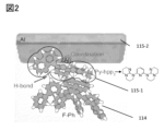
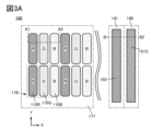

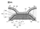


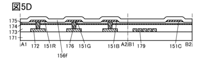


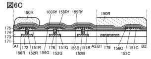
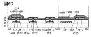

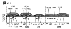


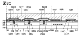

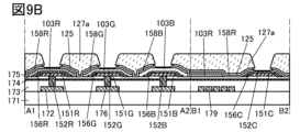
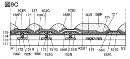


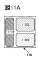
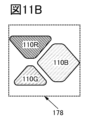

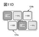


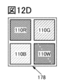


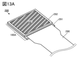


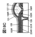


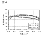


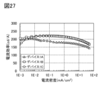


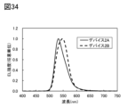
Classifications
-
- H—ELECTRICITY
- H10—SEMICONDUCTOR DEVICES; ELECTRIC SOLID-STATE DEVICES NOT OTHERWISE PROVIDED FOR
- H10K—ORGANIC ELECTRIC SOLID-STATE DEVICES
- H10K50/00—Organic light-emitting devices
- H10K50/10—OLEDs or polymer light-emitting diodes [PLED]
- H10K50/14—Carrier transporting layers
- H10K50/16—Electron transporting layers
-
- H—ELECTRICITY
- H10—SEMICONDUCTOR DEVICES; ELECTRIC SOLID-STATE DEVICES NOT OTHERWISE PROVIDED FOR
- H10K—ORGANIC ELECTRIC SOLID-STATE DEVICES
- H10K50/00—Organic light-emitting devices
- H10K50/10—OLEDs or polymer light-emitting diodes [PLED]
- H10K50/19—Tandem OLEDs
-
- H—ELECTRICITY
- H10—SEMICONDUCTOR DEVICES; ELECTRIC SOLID-STATE DEVICES NOT OTHERWISE PROVIDED FOR
- H10K—ORGANIC ELECTRIC SOLID-STATE DEVICES
- H10K50/00—Organic light-emitting devices
- H10K50/80—Constructional details
- H10K50/805—Electrodes
- H10K50/81—Anodes
-
- H—ELECTRICITY
- H10—SEMICONDUCTOR DEVICES; ELECTRIC SOLID-STATE DEVICES NOT OTHERWISE PROVIDED FOR
- H10K—ORGANIC ELECTRIC SOLID-STATE DEVICES
- H10K50/00—Organic light-emitting devices
- H10K50/80—Constructional details
- H10K50/805—Electrodes
- H10K50/82—Cathodes
-
- H—ELECTRICITY
- H10—SEMICONDUCTOR DEVICES; ELECTRIC SOLID-STATE DEVICES NOT OTHERWISE PROVIDED FOR
- H10K—ORGANIC ELECTRIC SOLID-STATE DEVICES
- H10K59/00—Integrated devices, or assemblies of multiple devices, comprising at least one organic light-emitting element covered by group H10K50/00
- H10K59/30—Devices specially adapted for multicolour light emission
- H10K59/35—Devices specially adapted for multicolour light emission comprising red-green-blue [RGB] subpixels
-
- H—ELECTRICITY
- H10—SEMICONDUCTOR DEVICES; ELECTRIC SOLID-STATE DEVICES NOT OTHERWISE PROVIDED FOR
- H10K—ORGANIC ELECTRIC SOLID-STATE DEVICES
- H10K59/00—Integrated devices, or assemblies of multiple devices, comprising at least one organic light-emitting element covered by group H10K50/00
- H10K59/90—Assemblies of multiple devices comprising at least one organic light-emitting element
-
- H—ELECTRICITY
- H10—SEMICONDUCTOR DEVICES; ELECTRIC SOLID-STATE DEVICES NOT OTHERWISE PROVIDED FOR
- H10K—ORGANIC ELECTRIC SOLID-STATE DEVICES
- H10K85/00—Organic materials used in the body or electrodes of devices covered by this subclass
- H10K85/30—Coordination compounds
-
- H—ELECTRICITY
- H10—SEMICONDUCTOR DEVICES; ELECTRIC SOLID-STATE DEVICES NOT OTHERWISE PROVIDED FOR
- H10K—ORGANIC ELECTRIC SOLID-STATE DEVICES
- H10K85/00—Organic materials used in the body or electrodes of devices covered by this subclass
- H10K85/60—Organic compounds having low molecular weight
Definitions
- One aspect of the present invention relates to a light-emitting device, a display module, and an electronic device.
- one embodiment of the present invention is not limited to the above technical field.
- Examples of the technical field of one embodiment of the present invention include semiconductor devices, light-emitting devices, power storage devices, memory devices, electronic devices, lighting devices, input devices (e.g., touch sensors), input/output devices (e.g., touch panels), driving methods thereof, and manufacturing methods thereof.
- Light-emitting devices also referred to as light-emitting elements
- EL electroluminescence
- the basic structure of these organic EL devices is to sandwich an organic compound layer containing a light-emitting material between a pair of electrodes. By applying a voltage to this device to inject carriers and utilizing the recombination energy of the carriers, light emission from the light-emitting material can be obtained.
- a light-emitting device also referred to as an EL device or an EL element
- a light-emitting device that utilizes the electroluminescence phenomenon has characteristics such as easy thinning and weight reduction, high-speed response to an input signal, and driveability using a DC constant-voltage power supply, and is applied to light-emitting devices.
- light-emitting devices are expected to be applied to various uses.
- applications of large light-emitting devices include home television devices (also referred to as televisions or television receivers), digital signage (digital signage), and PIDs (Public Information Displays).
- mobile information terminals such as smart phones and tablet terminals with touch panels are being developed.
- VR virtual reality
- AR augmented reality
- SR substitute reality
- MR mixed reality
- Patent Document 1 discloses a light-emitting device for VR using an organic EL device (also referred to as an organic EL element). Further, Patent Document 2 discloses a light-emitting device having a low driving voltage and good reliability, which uses a mixed film of a transition metal and an organic compound having a lone pair of electrons as an electron injection layer.
- One embodiment of the present invention is a light-emitting device including a first electrode, a second electrode, a first EL layer, an intermediate layer, and a second EL layer, wherein the first electrode is positioned to face the second electrode with the intermediate layer interposed therebetween, the first EL layer is positioned between the first electrode and the intermediate layer, the second EL layer is positioned between the intermediate layer and the second electrode, and the intermediate layer contains an organic compound represented by the following general formula (G1): There is.
- X is a group represented by the following general formula (G1-1)
- Y is a group represented by the following general formula (G1-2).
- R 1 and R 2 each independently represent hydrogen or deuterium
- h represents an integer of 1 to 6
- Ar represents a substituted or unsubstituted heteroaryl having 6 to 30 carbon atoms constituting a ring or an aryl having 6 to 30 carbon atoms constituting a substituted or unsubstituted ring.
- R3 to R6 each independently represent hydrogen or deuterium
- m represents an integer of 0 to 4
- n represents an integer of 1 to 5
- m+1 ⁇ n When m or n is 2 or more, R 3 to R 6 may be the same or different.
- another embodiment of the present invention includes a first electrode, a second electrode, a first EL layer, an intermediate layer, a second EL layer, and an organic compound layer, wherein the first electrode is positioned to face the second electrode with the intermediate layer interposed therebetween, the first EL layer is positioned between the first electrode and the intermediate layer, the second EL layer is positioned between the intermediate layer and the second electrode, and the organic compound layer is positioned between the second EL layer and the second electrode.
- 2 electrodes, and the intermediate layer and the organic compound layer include an organic compound represented by the following general formula (G1).
- X is a group represented by the following general formula (G1-1)
- Y is a group represented by the following general formula (G1-2).
- R 1 and R 2 each independently represent hydrogen or deuterium
- h represents an integer of 1 to 6
- Ar represents a substituted or unsubstituted heteroaryl having 6 to 30 carbon atoms constituting a ring or an aryl having 6 to 30 carbon atoms constituting a substituted or unsubstituted ring.
- R3 to R6 each independently represent hydrogen or deuterium
- m represents an integer of 0 to 4
- n represents an integer of 1 to 5
- m+1 ⁇ n When m or n is 2 or more, R 3 to R 6 may be the same or different.
- another embodiment of the present invention is a light-emitting device having the above structure, in which the organic compound included in the organic compound layer is included in a region in contact with the second EL layer.
- the organic compound layer includes one or more of a metal, a metal compound, and a metal complex.
- another embodiment of the present invention is a light-emitting device having the above structure, in which the organic compound layer has a stacked structure of a layer containing an organic compound and a layer containing one or more of a metal, a metal compound, and a metal complex.
- another embodiment of the present invention is a light-emitting device in which any one of the metal, the metal compound, and the metal complex is aluminum in the above structure.
- another embodiment of the present invention is a light-emitting device having the above structure, wherein the organic compound is an organic compound having a basic skeleton, and the basic skeleton has an acid dissociation constant pKa of 1 or more.
- another embodiment of the present invention is a light-emitting device having the above structure, in which the organic compound has a basic skeleton, and the basic skeleton has an acid dissociation constant pKa of 10 or more.
- another embodiment of the present invention is a light-emitting device having the above structure, in which the organic compound has a basic skeleton, and the basic skeleton has an acid dissociation constant pKa of 14 or more.
- another embodiment of the present invention is a light-emitting device having the above structure, in which the contours of the first electrode, the first EL layer, the intermediate layer, and the second EL layer are substantially the same.
- another embodiment of the present invention includes a first electrode, a second electrode, a first EL layer, an intermediate layer, and a second EL layer, wherein the first electrode is positioned to face the second electrode with the intermediate layer interposed therebetween, the first EL layer is positioned between the first electrode and the intermediate layer, the second EL layer is positioned between the intermediate layer and the second electrode, and the intermediate layer is an organic compound having a basic skeleton, wherein the basic
- the light-emitting device includes an organic compound having a skeleton with an acid dissociation constant pKa of 12 or more.
- another embodiment of the present invention includes a first electrode, a second electrode, a first EL layer, an intermediate layer, and a second EL layer, the first electrode facing the second electrode with the intermediate layer interposed therebetween, the first EL layer located between the first electrode and the intermediate layer, the second EL layer located between the intermediate layer and the second electrode, the first electrode, the first EL layer, and the intermediate layer;
- the contours of the second EL layer substantially match, and the intermediate layer is an organic compound having a basic skeleton, the basic skeleton having an acid dissociation constant pKa of 1 or more.
- another embodiment of the present invention includes a first electrode, a second electrode, a first EL layer, an intermediate layer, a second EL layer, and an organic compound layer, wherein the first electrode is positioned to face the second electrode with the intermediate layer interposed therebetween, the first EL layer is positioned between the first electrode and the intermediate layer, the second EL layer is positioned between the intermediate layer and the second electrode, and the organic compound layer is positioned between the second EL layer and the second electrode.
- 2 electrodes, the intermediate layer and the organic compound layer are organic compounds having a basic skeleton, and the basic skeleton has an acid dissociation constant pKa of 12 or more.
- another embodiment of the present invention includes a first electrode, a second electrode, a first EL layer, an intermediate layer, a second EL layer, and an organic compound layer, the first electrode facing the second electrode with the intermediate layer therebetween, the first EL layer located between the first electrode and the intermediate layer, the second EL layer located between the intermediate layer and the second electrode, and the first electrode and the first EL layer.
- the intermediate layer and the second EL layer have substantially the same outline
- the organic compound layer is located between the second EL layer and the second electrode
- the intermediate layer and the organic compound layer are organic compounds having a basic skeleton
- the basic skeleton has an acid dissociation constant pKa of 1 or more.
- another embodiment of the present invention is a light-emitting device having the above structure, in which the organic compound included in the organic compound layer is included in a region in contact with the second EL layer.
- the organic compound layer includes one or more of a metal, a metal compound, and a metal complex.
- another embodiment of the present invention is a light-emitting device having the above structure, in which the organic compound layer has a stacked structure of a layer containing an organic compound and a layer containing one or more of a metal, a metal compound, and a metal complex.
- another embodiment of the present invention is a light-emitting device in which any one of the metal, the metal compound, and the metal complex is aluminum in the above structure.
- another embodiment of the present invention is a light-emitting device in which the intermediate layer includes one or more of a metal, a metal compound, and a metal complex in the above structure.
- another embodiment of the present invention is a light-emitting device having the above structure, in which the intermediate layer has a stacked structure of a layer containing an organic compound and a layer containing one or more of a metal, a metal compound, and a metal complex.
- another embodiment of the present invention is a light-emitting device in which any one of the metal, the metal compound, and the metal complex is aluminum in the above structure.
- the organic compound included in the intermediate layer is included in a region in contact with the first EL layer.
- another embodiment of the present invention is a light-emitting device having the above structure, in which the organic compound has a 1,3,4,6,7,8-hexahydro-2H-pyrimido[1,2-a]pyridine skeleton and a heteroaryl ring having 2 to 30 carbon atoms.
- another embodiment of the present invention is a light-emitting device having the above structure, in which the organic compound is an organic compound represented by any one of General Formulas (G2-1) to (G2-6) below.
- R 11 to R 26 each independently represent hydrogen or deuterium
- h represents an integer of 1 to 6
- Ar is an organic compound in which a substituted or unsubstituted ring-constituting carbon atom of 6 to 30 heteroaryl or a substituted or unsubstituted ring-constituting carbon atom of 6 to 30 aryl.
- another embodiment of the present invention is a light-emitting device in which the heteroaryl having 6 to 30 carbon atoms constituting the substituted or unsubstituted ring represented by Ar or the aryl having 6 to 30 carbon atoms constituting the substituted or unsubstituted ring is represented by any one of the following structural formulas (Ar-1) to (Ar-27).
- another embodiment of the present invention is a light-emitting device in which, in the above structure, Ar contains nitrogen as a ring-constituting element, and Ar is bonded to the parenthesized skeleton in General Formula (G1) through a bond of nitrogen or a carbon adjacent to nitrogen.
- another embodiment of the present invention is a light-emitting device having the above structure, in which the organic compound has a bicyclo ring structure in which 2 or more nitrogen atoms are contained in the ring-constituting elements, and heteroaryl or aryl having 6 to 30 carbon atoms in the ring.
- another embodiment of the present invention is a light-emitting device having the above structure, in which the intermediate layer has a thickness of 1 nm or less.
- another embodiment of the present invention is a light-emitting device having the above structure, in which the intermediate layer has a thickness of 0.5 nm or less.
- another embodiment of the present invention is a light-emitting device having the above structure, which includes a second intermediate layer and a third EL layer between the first electrode and the second electrode.
- One embodiment of the present invention can provide a light-emitting device with high display quality.
- one embodiment of the present invention can provide a high-definition light-emitting device.
- one embodiment of the present invention can provide a light-emitting device with high resolution.
- one embodiment of the present invention can provide a highly reliable light-emitting device.
- one embodiment of the present invention can provide a novel light-emitting device with excellent convenience, usefulness, or reliability.
- one embodiment of the present invention can provide a novel display module with excellent convenience, usefulness, or reliability.
- a novel light-emitting device, a novel display module, a novel electronic device, or a novel semiconductor device can be provided.
- FIG. 1A-1C are diagrams representing a light emitting device.
- FIG. 2 is a diagram illustrating the interaction between the organic compound represented by general formula (G1) and aluminum.
- 3A and 3B are top and cross-sectional views of a light emitting device.
- 4A-4D are diagrams representing a light emitting device.
- 5A to 5E are cross-sectional views illustrating an example of a method for manufacturing a light-emitting device.
- 6A to 6D are cross-sectional views illustrating an example of a method for manufacturing a light-emitting device.
- 7A to 7D are cross-sectional views illustrating an example of a method for manufacturing a light-emitting device.
- FIG. 8A to 8C are cross-sectional views illustrating an example of a method for manufacturing a light-emitting device.
- 9A to 9C are cross-sectional views illustrating an example of a method for manufacturing a light-emitting device.
- 10A to 10C are cross-sectional views illustrating an example of a method for manufacturing a light-emitting device.
- 11A to 11G are top views showing configuration examples of pixels.
- 12A to 12I are top views showing configuration examples of pixels.
- 13A and 13B are perspective views showing configuration examples of the display module.
- 14A and 14B are cross-sectional views showing configuration examples of light-emitting devices.
- FIG. 15 is a perspective view showing a configuration example of a light emitting device.
- FIG. 15 is a perspective view showing a configuration example of a light emitting device.
- 16A is a cross-sectional view showing a configuration example of a light emitting device.
- 16B and 16C are cross-sectional views showing configuration examples of transistors.
- FIG. 17 is a cross-sectional view showing a configuration example of a light emitting device.
- 18A to 18D are cross-sectional views showing configuration examples of light emitting devices.
- 19A to 19D are diagrams illustrating examples of electronic devices.
- 20A to 20F are diagrams illustrating examples of electronic devices.
- 21A to 21G are diagrams illustrating examples of electronic devices.
- FIG. 22 is a diagram for explaining the structure of a sample according to this example.
- FIG. 23 is a diagram showing luminance-current density characteristics of the sample according to the present example.
- FIG. 24 is a diagram showing the current efficiency-luminance characteristics of the sample according to this example.
- FIG. 25 is a diagram showing the luminance-voltage characteristics of the sample according to this example.
- FIG. 26 is a diagram showing the current density-voltage characteristics of the sample according to this example.
- FIG. 27 is a diagram showing the current efficiency-current density characteristics of the sample according to this example.
- FIG. 28 is a diagram showing the electroluminescence spectrum of the sample according to this example.
- FIG. 29 is a diagram showing luminance-current density characteristics of the sample according to the present example.
- FIG. 30 is a diagram showing the current efficiency-luminance characteristics of the sample according to this example.
- FIG. 31 is a diagram showing luminance-voltage characteristics of the sample according to this example.
- FIG. 32 is a diagram showing the current density-voltage characteristics of the sample according to this example.
- FIG. 33 is a diagram showing the current efficiency-current density characteristics of the sample according to this example.
- FIG. 34 is a diagram showing the electroluminescence spectrum of the sample according to this example.
- film and “layer” can be interchanged depending on the case or situation.
- conductive layer can be changed to the term “conductive film.”
- insulating film can be changed to the term “insulating layer”.
- a device manufactured using a metal mask or FMM may be referred to as a device with an MM (metal mask) structure.
- a device manufactured without using a metal mask or FMM may be referred to as a device with an MML (metal maskless) structure.
- holes or electrons are sometimes referred to as “carriers”.
- the hole injection layer or electron injection layer may be referred to as a "carrier injection layer”
- the hole transport layer or electron transport layer may be referred to as a “carrier transport layer”
- the hole blocking layer or electron blocking layer may be referred to as a "carrier blocking layer”.
- the carrier injection layer, the carrier transport layer, and the carrier block layer described above may not be clearly distinguished from each other due to their cross-sectional shape, characteristics, or the like.
- one layer may serve as two or three functions of the carrier injection layer, the carrier transport layer, and the carrier block layer.
- a light-emitting device (also referred to as a light-emitting element) includes an EL layer between a pair of electrodes.
- the EL layer has at least a light-emitting layer.
- a light-receiving device (also referred to as a light-receiving element) has at least an active layer functioning as a photoelectric conversion layer between a pair of electrodes.
- one of a pair of electrodes may be referred to as a pixel electrode and the other may be referred to as a common electrode.
- a tapered shape refers to a shape in which at least a part of the side surface of the structure is inclined with respect to the substrate surface. For example, it is preferable to have a region where the angle between the inclined side surface and the substrate surface (also referred to as a taper angle) is less than 90°. Note that the side surfaces of the structure and the substrate surface are not necessarily completely flat, and may be substantially planar with a fine curvature or substantially planar with fine unevenness.
- the light-emitting device in this specification includes an image display device using an organic EL device.
- the light emitting device may also include a module in which a connector such as an anisotropic conductive film or TCP (Tape Carrier Package) is attached to the organic EL device, a module in which a printed wiring board is provided in front of the TCP, or a module in which an IC (integrated circuit) is directly mounted on the organic EL device by the COG (Chip On Glass) method.
- a connector such as an anisotropic conductive film or TCP (Tape Carrier Package) is attached to the organic EL device
- a module in which a printed wiring board is provided in front of the TCP
- IC integrated circuit
- lighting fixtures and the like may have light emitting devices.
- An organic EL element (hereinafter also referred to as a light-emitting device) has an organic compound layer (corresponding to the organic semiconductor film) containing a light-emitting substance between electrodes (between a first electrode and a second electrode), and has a configuration in which light is emitted by energy generated by recombination of carriers (holes and electrons) injected into the organic compound layer from the electrodes.
- FIG. 1A shows a light emitting device 130 according to one aspect of the invention.
- a light-emitting device of one embodiment of the present invention is a tandem-type light-emitting device including a first light-emitting unit 501 including a first light-emitting layer 113_1, a second light-emitting unit 502 including a second light-emitting layer 113_2, and an organic compound layer 103 having an intermediate layer 116 between a first electrode 101 including an anode and a second electrode 102 including a cathode (a light-emitting unit is also referred to as an EL layer).
- a light-emitting device having one intermediate layer 116 and two light-emitting units will be described as an example, but a light-emitting device having n (n is an integer equal to or greater than 1) layers of charge generation layers and n+1 layers of light-emitting units may also be used.
- the light emitting device 130 shown in FIG. 1B is an example of a tandem light emitting device where n is 2, having a first light emitting unit 501, a first intermediate layer 116_1, a second light emitting unit 502, a second intermediate layer 116_2, and a third light emitting unit 503.
- intermediate layer 116 has at least P-type layer 117 (hereinafter also referred to as charge generation region) and N-type layer 119 (hereinafter also referred to as electron injection buffer region). Between the N-type layer 119 and the P-type layer 117, an electron relay layer 118 (hereinafter also referred to as an electron relay region) may be provided for smooth transfer of electrons between the two layers.
- the color gamut of light exhibited by the light-emitting layer in each light-emitting unit may be the same or different.
- the light-emitting layer may have a single layer structure or a laminated structure.
- white light emission can be obtained by a configuration in which the first light emitting unit and the third light emitting unit emit light in the blue region, and the second light emitting unit emits light in the red region and green region from the light emitting layers of the laminated structure.
- the light-emitting device of one embodiment of the present invention may be a light-emitting device manufactured by a lithography method such as a photolithography method, for example.
- a lithography method such as a photolithography method, for example.
- photolithography at least the second light-emitting layer 113_2 and the organic compound layer closer to the first electrode 101 than the second light-emitting layer 113_2 are processed at the same time, so that the edges thereof are substantially aligned in the vertical direction.
- an alkali metal such as lithium (Li) or a compound of the alkali metal is used for the N-type layer of the intermediate layer or the electron injection layer, and the voltage reduction is realized.
- a tandem-type light-emitting device has a structure in which a plurality of light-emitting layers are stacked in series with an intermediate layer interposed therebetween, and the intermediate layer includes a layer of an alkali metal or a compound of the alkali metal in order to inject electrons into the light-emitting unit in contact with the anode. That is, compared to a single-type light-emitting device, the tandem-type light-emitting device has a higher probability that the alkali metal or alkali metal compound layer reacts with atmospheric components such as water or oxygen.
- the intermediate layer is exposed to the air, resist resin, water, chemical solutions, etc. during the processing process, so that the layer of the alkali metal or the compound of the alkali metal inevitably deteriorates the characteristics significantly.
- exposure of the alkali metal or alkali metal compound layer in the intermediate layer to the photolithography process causes a significant increase in driving voltage and a significant decrease in luminous efficiency, as in the case of exposing the electron injection layer to the photolithography process.
- the present inventors have found that the occurrence of problems caused by the alkali metal or the alkali metal compound can be reduced.
- n is an integer of 1 or more intermediate layers and n+1 light-emitting units
- at least one of the n intermediate layers contains an organic compound represented by the following general formula (G1) having a basic skeleton.
- X is a group represented by the following general formula (G1-1)
- Y is a group represented by the following general formula (G1-2).
- R 1 and R 2 each independently represent hydrogen or deuterium
- h represents an integer of 1 to 6
- Ar represents a heteroaryl having 6 to 30 carbon atoms constituting a substituted or unsubstituted ring, or an aryl having 6 to 30 carbon atoms constituting a substituted or unsubstituted ring.
- R3 to R6 each independently represent hydrogen or deuterium
- m represents an integer of 0 to 4
- n represents an integer of 1 to 5
- m+1 ⁇ n When m or n is 2 or more, the plurality of R 3 to R 6 may be the same or different.
- organic compound represented by General Formula (G1) is preferably any one of General Formulas (G2-1) to (G2-6) below.
- R 11 to R 26 each independently represent hydrogen or deuterium
- h represents an integer of 1 to 6
- Ar is an organic compound in which a substituted or unsubstituted ring-constituting carbon atom of 6 to 30 heteroaryl or a substituted or unsubstituted ring-constituting carbon atom of 6 to 30 aryl.
- heteroaryl skeleton having 6 to 30 carbon atoms constituting the substituted or unsubstituted ring represented by Ar include pyridine, bipyridine, pyrimidine, bipyrimidine, pyrazine, bipyrazine, triazine, quinoline, isoquinoline, benzoquinoline, phenanthroline, quinoxaline, benzoquinoxaline, Dibenzoquinoxaline, azofluorene, diazofluorene, carbazole, benzocarbazole, dibenzocarbazole, dibenzofuran, benzonaphthofuran, dinaphthofuran, dibenzothiophene, benzonaphthothiophene, dinaphthothiophene, benzofuropyridine, benzofuropyrimidine, benzothiopyridine, benzothiopyrimidine, naph
- any one of the following structural formulas (Ar-1) to (Ar-27) is preferable.
- Ar contains nitrogen as a ring-constituting element, and Ar is bound to the skeleton in parentheses in General Formula (G1) through a bond of the nitrogen or a carbon adjacent to the nitrogen.
- organometallic compounds represented by General Formula (G1) and General Formulas (G2-1) to (G2-6) include organic compounds represented by Structural Formulas (100) to (109) below.
- the organic compound represented by General Formula (G1) having a basic skeleton is preferably an organic compound in which the basic skeleton has an acid dissociation constant pKa of 7 or more, preferably 10 or more. Further, it is more preferably an organic compound in which the basic skeleton has an acid dissociation constant pKa of 12 or more, more preferably an organic compound in which the basic skeleton has an acid dissociation constant pKa of 13 or more, and even more preferably an organic compound in which the basic skeleton has an acid dissociation constant pKa of 14 or more.
- the value of an organic compound in which a part of the skeleton is substituted with hydrogen can be used.
- the acid dissociation constant pKa of the organic compound having a basic skeleton the acid dissociation constant pKa of the basic skeleton can be used.
- the acid dissociation constant pKa of the basic skeleton having the highest acid dissociation constant pKa can be used as the acid dissociation constant pKa of the organic compound.
- the acid dissociation constant pKa is preferably a value measured using water as a solvent.
- the most stable structure (singlet ground state) obtained from the first-principles calculation is used as the initial structure of the molecular structure of each molecule to be a calculation model.
- the pKa calculation designates one or more atoms of each molecule as basic sites, uses the Macro Model to search for stable structures of protonated molecules in water, performs conformational searches using the OPLS2005 force field, and uses the lowest energy conformers.
- Jaguar's pKa calculation module geometry optimization with B3LYP/6-31G* followed by single point calculation with cc-pVTZ(+) and pKa values are calculated using empirical corrections for functional groups. For molecules that designate more than one atom as a basic site, the highest value obtained is taken as the pKa value.
- organic compounds having a high acid dissociation constant pKa include organic compounds having basic skeletons represented by the following structural formulas (120) to (123).
- the acid dissociation constant pKa of DBU represented by structural formula (120) is 11.9
- the acid dissociation constant pKa of DBN represented by structural formula (121) is 12.7
- the acid dissociation constant pKa of TBD represented by structural formula (122) is 14.5
- the acid dissociation constant pKa of MTBD represented by structural formula (123) is 13.0. All values are measured using water as a solvent.
- the acid dissociation constant pKa of 1,10-phenanthroline is 4.8
- the acid dissociation constant pKa of benzimidazole is 5.5
- the acid dissociation constant pKa of imidazole is 6.9
- the acid dissociation constant pKa of pyridine is 5.3
- the acid dissociation constant pKa of pyrimidine is 1.1.
- a compound having a basic skeleton with a high acid dissociation constant pKa is known to form hydrogen bonds with hydrogen atoms of other molecules.
- the physical properties of the material change due to this hydrogen bond, and the performance as an N-type layer or an electron injection layer may be ensured.
- one or both of the electron injection layer and the N-type intermediate layer may contain one or more of a metal, a metal compound, and a metal complex in addition to the organic compound having the basic skeleton.
- the metal, metal compound, and metal complex may be any metal that can be coordinated to an organic compound having a basic skeleton, such as a metal compound such as a metal oxide, or a metal complex.
- a metal compound such as a metal oxide, or a metal complex.
- aluminum (Al) and molybdenum (Mo) can be used as the metal.
- metal compounds aluminum zinc oxide, indium zinc oxide containing aluminum, molybdenum oxide, vanadium oxide, ruthenium oxide, tungsten oxide, and manganese oxide can be used.
- metal complexes examples include tris(8-quinolinolato)aluminum (abbreviation: Alq 3 ), tris(4-methyl-8-quinolinolato)aluminum (abbreviation: Almq 3 ), bis(10-hydroxybenzo[h]quinolinato)beryllium (II) (abbreviation: BeBq 2 ), and bis(2-methyl-8-quinolinolato)(4-phenylphenolato)aluminum (III). (abbreviation: BAlq) can be used. Note that a plurality of the above-described metals, metal compounds, and metal complexes may be used in combination.
- the electron injection layer or the N-type layer of the intermediate layer contains one or more of a metal, a metal compound, and a metal complex, as shown in FIG. 2, the interaction (coordination) between the organic compound having a basic skeleton and the metal, the metal compound, and the metal complex improves the electron injectability, and a light-emitting device in which an increase in driving voltage is suppressed can be obtained without using an alkali metal or the like.
- It may be a mixed layer of an organic compound having a basic skeleton and one or more of a metal, a metal compound, and a metal complex, or a layered structure of a layer containing the organic compound and a layer containing one or more of a metal, a metal compound, and a metal complex.
- the layer containing one or more of a metal, a metal compound, and a metal complex preferably exists closest to the second electrode 102 side.
- the first light-emitting unit 501 and the second light-emitting unit may include other functional layers in addition to the light-emitting layer.
- the first light-emitting unit 501 includes the hole injection layer 111, the first hole-transport layer 112_1, and the first electron-transport layer 114_1 in addition to the first light-emitting layer 113_1
- the second light-emitting unit 502 includes the second hole-transport layer 112_2, the second electron-transport layer 114_2, and the electron injection layer 115 in addition to the second light-emitting layer 113_2.
- the structure of the organic compound layer 103 in the present invention is not limited to this, and any layer may be omitted or another layer may be provided.
- other layers typically include a carrier block layer, an exciton block layer, and the like.
- the intermediate layer 116 since the intermediate layer 116 has the N-type layer 119, the N-type layer 119 plays a role of an electron injection layer in the anode-side light-emitting unit. Therefore, the electron-injection layer may be provided in the anode-side light-emitting unit (the first light-emitting unit 501 in FIG. 1A) as necessary.
- the intermediate layer 116 since the intermediate layer 116 has the P-type layer 117, the P-type layer 117 plays a role of a hole injection layer in the cathode-side light-emitting unit, so the cathode-side light-emitting unit (the second light-emitting unit 502 in FIG. 1A) may be provided with a hole injection layer as necessary.
- the N-type layer 119 is a layer containing the organic compound represented by the general formula (G1) having a basic skeleton, but the layer may be a mixture of any one or more of a metal, a metal compound, and a metal complex.
- the P-type layer 117 which is a charge generation layer, is preferably formed from a composite material containing a material having an acceptor property and an organic compound having a hole transport property.
- a composite material containing a material having an acceptor property and an organic compound having a hole transport property.
- organic compounds such as aromatic amine compounds, heteroaromatic compounds, aromatic hydrocarbons, and polymer compounds (oligomers, dendrimers, polymers, etc.) can be used as the hole-transporting organic compound used in the composite material.
- an organic compound having a hole-transport property used for the composite material is preferably an organic compound having a hole mobility of 1 ⁇ 10 ⁇ 6 cm 2 /Vs or more.
- the hole-transporting organic compound used for the composite material is preferably a compound having a condensed aromatic hydrocarbon ring or a ⁇ -electron rich heteroaromatic ring.
- the condensed aromatic hydrocarbon ring anthracene ring, naphthalene ring and the like are preferable.
- the ⁇ -electron-rich heteroaromatic ring is preferably a condensed aromatic ring containing at least one of a pyrrole skeleton, a furan skeleton, and a thiophene skeleton in the ring.
- a carbazole ring, a dibenzothiophene ring, or a ring in which an aromatic ring or a heteroaromatic ring is further condensed is preferred.
- Such an organic compound having a hole-transporting property preferably has any one of a carbazole skeleton, a dibenzofuran skeleton, a dibenzothiophene skeleton, and an anthracene skeleton.
- it may be an aromatic amine having a substituent containing a dibenzofuran ring or a dibenzothiophene ring, an aromatic monoamine having a naphthalene ring, or an aromatic monoamine having a 9-fluorenyl group bonded to the nitrogen of the amine via an arylene group.
- a substance having an N,N-bis(4-biphenyl)amino group is preferably used as the hole-transporting organic compound because a light-emitting device with a long life can be manufactured.
- organic compounds having hole transport properties include N-(4-biphenyl)-6,N-diphenylbenzo[b]naphtho[1,2-d]furan-8-amine (abbreviation: BnfABP), N,N-bis(4-biphenyl)-6-phenylbenzo[b]naphtho[1,2-d]furan-8-amine (abbreviation: BBABnf), 4,4'-bis(6-phenylbenzo[ b]naphtho[1,2-d]furan-8-yl)-4′′-phenyltriphenylamine (abbreviation: BnfBB1BP), N,N-bis(4-biphenyl)benzo[b]naphtho[1,2-d]furan-6-amine (abbreviation: BBABnf(6)), N,N-bis(4-biphenyl)benzo[b]naphtho[1,2-d]furan-8-amine (
- DTDPPA N,N'-di(p-tolyl)-N,N'-diphenyl-p-phenylenediamine
- DPAB 4,4'-bis[N-(4-diphenylaminophenyl)-N-phenylamino]biphenyl
- DNTPD 1,3,5-tris[N-(4-diphenylaminophenyl)-N-phenylamino]benzene
- DPA3B 1,3,5-tris[N-(4-diphenylaminophenyl)-N-phenylamino]benzene
- an organic compound having an electron-withdrawing group (halogen group, cyano group, or the like) can be used.
- rene abbreviation: HAT-CN
- 1,3,4,5,7,8-hexafluorotetracyano-naphthoquinodimethane abbreviation: F6-TCNNQ
- 2-(7-dicyanomethylene-1,3,4,5,6,8,9,10-octafluoro-7H-pyrene-2-ylidene)malononitrile and the like.
- a compound in which an electron-withdrawing group is bound to a condensed aromatic ring having a plurality of heteroatoms such as HAT-CN
- radialene derivatives having an electron-withdrawing group are preferable because of their extremely high electron-accepting properties.
- 3,5-difluoro-4-(trifluoromethyl)benzeneacetonitrile] ⁇ , ⁇ ′, ⁇ ′′-1,2,3-cyclopropanetriylidene tris[2,3,4,5,6-pentafluorobenzeneacetonitrile] and the like.
- transition metal oxides such as molybdenum oxide, vanadium oxide, ruthenium oxide, tungsten oxide, and manganese oxide can be used in addition to the organic compounds described above.
- the electron relay layer 118 contains an electron-transporting substance, and has a function of preventing interaction between the N-type layer 119 and the P-type layer 117 and transferring electrons smoothly.
- the LUMO level of the substance having an electron transport property contained in the electron relay layer 118 is preferably between the LUMO level of the acceptor substance in the P-type layer 117 and the LUMO level of the organic compound contained in the layer in contact with the intermediate layer 116 in the light-emitting unit on the first electrode 101 side (the first electron-transporting layer 114_1 in the first light-emitting unit 501 in FIG. 1A).
- a specific energy level of the LUMO level in the substance having an electron-transport property used for the electron relay layer 118 is ⁇ 5.0 eV or more, preferably ⁇ 5.0 eV or more and ⁇ 3.0 eV or less.
- a phthalocyanine-based material or a metal complex having a metal-oxygen bond and an aromatic ligand is preferably used as a substance having an electron-transporting property that is used for the electron-relay layer 118 .
- a tandem-type light-emitting device having such an intermediate layer 116 can be a light-emitting device having good characteristics without causing a significant increase in driving voltage and a significant decrease in luminous efficiency even when the organic compound layer 103 is processed by photolithography.
- the first electrode 101 is an electrode including an anode.
- the first electrode 101 may have a laminated structure, in which case the layer in contact with the organic compound layer 103 functions as an anode.
- the anode is preferably formed using a metal, an alloy, a conductive compound, a mixture thereof, or the like having a large work function (specifically, 4.0 eV or more).
- Specific examples include indium oxide-tin oxide (ITO), indium oxide-tin oxide containing silicon or silicon oxide, indium oxide-zinc oxide, and indium oxide containing tungsten oxide and zinc oxide (IWZO).
- ITO indium oxide-tin oxide
- IWZO indium oxide containing tungsten oxide and zinc oxide
- These conductive metal oxide films are usually formed by a sputtering method, but may be produced by applying a sol-gel method or the like.
- indium oxide-zinc oxide is formed by a sputtering method using a target in which 1 to 20 wt % of zinc oxide is added to indium oxide.
- Indium oxide (IWZO) containing tungsten oxide and zinc oxide can also be formed by a sputtering method using a target containing 0.5 to 5 wt % tungsten oxide and 0.1 to 1 wt % zinc oxide relative to indium oxide.
- materials used for the anode include, for example, gold (Au), platinum (Pt), nickel (Ni), tungsten (W), chromium (Cr), molybdenum (Mo), iron (Fe), cobalt (Co), copper (Cu), palladium (Pd), and nitrides of metal materials (e.g., titanium nitride).
- metal materials e.g., titanium nitride
- graphene can also be used as the material used for the anode.
- FIG. 1A shows a stacked structure including a first light-emitting unit 501 including a first light-emitting layer 113_1 and a second light-emitting unit 502 including an intermediate layer 116 and a second light-emitting layer 113_2.
- a configuration in which two light-emitting units are stacked with an intermediate layer interposed is shown here, a configuration in which three or more light-emitting units are stacked may be used. Also in this case, an intermediate layer is provided between the light emitting units.
- Each light emitting unit also has a laminated structure.
- the light-emitting unit is not limited to the configuration shown in FIG. 1A, and can be configured by appropriately using various functional layers such as a hole injection layer, a hole transport layer, an electron transport layer, an electron injection layer, a carrier block layer (hole block layer, electron block layer), and an exciton block layer.
- the hole injection layer 111 is provided in contact with the anode and has a function of facilitating the injection of holes into the organic compound layer 103 (first light emitting unit 501).
- the hole injection layer 111 is made of phthalocyanine-based complex compounds such as phthalocyanine (abbreviation: H 2 Pc) and copper phthalocyanine (abbreviation: CuPc); It can be formed from an aromatic amine compound such as DNTPD) or a polymer such as poly(3,4-ethylenedioxythiophene)/(polystyrenesulfonic acid) (abbreviation: PEDOT/PSS).
- the hole-injection layer 111 may be formed using a substance having an electron acceptor property.
- the substance having acceptor properties the substances exemplified as the acceptor substances used for the composite material forming the P-type layer 117 in the intermediate layer 116 can be used in the same manner.
- the hole injection layer 111 may be formed by similarly using the composite material forming the P-type layer 117 in the intermediate layer 116 .
- the hole-transporting organic compound used for the composite material is more preferably a substance with a relatively deep HOMO level of ⁇ 5.7 eV to ⁇ 5.4 eV. Since the organic compound having a hole-transporting property used in the composite material has a relatively deep HOMO level, it becomes easy to inject holes into the hole-transporting layer and to obtain a light-emitting device with a good lifetime. In addition, since the organic compound having a hole-transporting property used in the composite material is a substance having a relatively deep HOMO level, the induction of holes is appropriately suppressed, and a light-emitting device having a long life can be obtained.
- the hole-injection layer 111 By forming the hole-injection layer 111, the hole-injection property is improved, and a light-emitting device with a low driving voltage can be obtained.
- organic compounds having acceptor properties are easy to use because they are easily vapor-deposited and easily formed into a film.
- the second light emitting unit 502 is not provided with a hole injection layer, but the second light emission unit may be provided with a hole injection layer.
- the hole-transport layer 112 (the first hole-transport layer 112_1 and the second hole-transport layer 112_2) contains an organic compound having a hole-transport property.
- the organic compound having a hole-transport property preferably has a hole mobility of 1 ⁇ 10 ⁇ 6 cm 2 /Vs or more.
- hole-transporting material examples include 4,4'-bis[N-(1-naphthyl)-N-phenylamino]biphenyl (abbreviation: NPB), N,N'-diphenyl-N,N'-bis(3-methylphenyl)-4,4'-diaminobiphenyl (abbreviation: TPD), 4,4'-bis(9,9'-spirobi[9H-fluoren]-2-yl)-N,N'-diphenyl-4,4 '-diaminobiphenyl (abbreviation: BSPB), 4-phenyl-4'-(9-phenylfluoren-9-yl)triphenylamine (abbreviation: BPAFLP), 4-phenyl-3'-(9-phenylfluoren-9-yl)triphenylamine (abbreviation: mBPAFLP), 4-phenyl-4'-(9-phenyl-9H-carbazol-3-yl
- compounds having an aromatic amine skeleton or compounds having a carbazole skeleton are preferable because they have good reliability, high hole-transport properties, and contribute to reduction in driving voltage.
- the substances exemplified as the materials having a hole-transport property that are used for the composite material of the hole-injection layer 111 can also be suitably used as the material for the hole-transport layer 112 .
- the light-emitting layer 113 (the first light-emitting layer 113_1 and the second light-emitting layer 113_2) preferably contains a light-emitting substance and a host material. Note that the light-emitting layer may contain other materials at the same time. Alternatively, a laminate of two layers having different compositions may be used.
- the luminescent substance may be a fluorescent luminescent substance, a phosphorescent luminescent substance, a substance exhibiting thermally activated delayed fluorescence (TADF), or any other luminescent substance.
- TADF thermally activated delayed fluorescence
- Examples of materials that can be used as fluorescent light-emitting substances in the light-emitting layer include the following. Fluorescent substances other than these can also be used.
- condensed aromatic diamine compounds typified by pyrenediamine compounds such as 1,6FLPAPrn, 1,6mMemFLPAPrn, and 1,6BnfAPrn-03 are preferable because of their high hole-trapping properties and excellent luminous efficiency or reliability.
- usable materials include, for example, the following.
- known phosphorescent compounds may be selected and used.
- Fullerene and its derivatives, acridine and its derivatives, eosin derivatives and the like can be used as the TADF material.
- metal-containing porphyrin examples include protoporphyrin-tin fluoride complex ( SnF2 (Proto IX)), mesoporphyrin-tin fluoride complex ( SnF2 (Meso IX ) ), hematoporphyrin-tin fluoride complex (SnF2 (Hemato IX)), coproporphyrin tetramethyl ester-tin fluoride complex ( SnF2 (Cop ro III-4Me)), octaethylporphyrin-tin fluoride complex ( SnF2 (OEP)), ethioporphyrin-tin fluoride complex ( SnF2 (Etio I)), octaethylporphyrin-platinum chloride complex ( PtCl2OEP ), and the like.
- SnF2 Proto IX
- SnF2 mesoporphyrin-tin fluor
- the heterocyclic compound has a ⁇ -electron-rich heteroaromatic ring and a ⁇ -electron-deficient heteroaromatic ring
- the heterocyclic compound has both high electron-transporting properties and high hole-transporting properties, which is preferable.
- a pyridine skeleton, a diazine skeleton (pyrimidine skeleton, pyrazine skeleton, pyridazine skeleton), and a triazine skeleton are preferred because they are stable and reliable.
- a benzofuropyrimidine skeleton, a benzothienopyrimidine skeleton, a benzofuropyrazine skeleton, and a benzothienopyrazine skeleton are preferred because they have high acceptor properties and good reliability.
- an acridine skeleton, a phenoxazine skeleton, a phenothiazine skeleton, a furan skeleton, a thiophene skeleton, and a pyrrole skeleton are stable and reliable, so it is preferable to have at least one of the skeletons.
- a dibenzofuran skeleton is preferable as the furan skeleton, and a dibenzothiophene skeleton is preferable as the thiophene skeleton.
- a dibenzothiophene skeleton is preferable as the thiophene skeleton.
- an indole skeleton, a carbazole skeleton, an indolocarbazole skeleton, a bicarbazole skeleton, and a 3-(9-phenyl-9H-carbazol-3-yl)-9H-carbazole skeleton are particularly preferred.
- a substance in which a ⁇ -electron-rich heteroaromatic ring and a ⁇ -electron-deficient heteroaromatic ring are directly bonded is particularly preferable because both the electron-donating property of the ⁇ -electron-rich heteroaromatic ring and the electron-accepting property of the ⁇ -electron-deficient heteroaromatic ring are strong, and the energy difference between the S1 level and the T1 level is small, so that thermally activated delayed fluorescence can be obtained efficiently.
- An aromatic ring to which an electron-withdrawing group such as a cyano group is bonded may be used instead of the ⁇ -electron-deficient heteroaromatic ring.
- an aromatic amine skeleton, a phenazine skeleton, or the like can be used as the ⁇ -electron-rich skeleton.
- a xanthene skeleton, a thioxanthene dioxide skeleton, an oxadiazole skeleton, a triazole skeleton, an imidazole skeleton, an anthraquinone skeleton, a boron-containing skeleton such as phenylborane and borantrene, an aromatic ring having a nitrile group or a cyano group such as benzonitrile or cyanobenzene, a heteroaromatic ring, a carbonyl skeleton such as benzophenone, a phosphine oxide skeleton, a sulfone skeleton, and the like can be used.
- a ⁇ -electron-deficient skeleton and a ⁇ -electron-rich skeleton can be used in place of at least one of the ⁇ -electron-deficient heteroaromatic ring and the ⁇ -electron-rich heteroaromatic ring.
- a TADF material in which a singlet excited state and a triplet excited state are in thermal equilibrium may be used as the TADF material. Since such a TADF material has a short emission lifetime (excitation lifetime), it is possible to suppress a decrease in efficiency in a high-luminance region of a light-emitting device. Specifically, materials such as those having the molecular structures shown below are exemplified.
- the TADF material is a material having a small difference between the S1 level and the T1 level and having a function of converting energy from triplet excitation energy to singlet excitation energy by reverse intersystem crossing. Therefore, triplet excitation energy can be up-converted (reverse intersystem crossing) to singlet excitation energy with a small amount of thermal energy, and a singlet excited state can be efficiently generated. Also, triplet excitation energy can be converted into luminescence.
- an exciplex (also referred to as an exciplex, an exciplex, or an exciplex) in which two kinds of substances form an excited state has an extremely small difference between the S1 level and the T1 level, and functions as a TADF material capable of converting triplet excitation energy into singlet excitation energy.
- a phosphorescence spectrum observed at a low temperature may be used as an index of the T1 level.
- a tangent line is drawn on the short wavelength side of the fluorescence spectrum, the energy of the wavelength of the extrapolation line is the S1 level, and the tangent line is drawn on the short wavelength side of the phosphorescence spectrum, and the energy of the wavelength of the extrapolation line is the T1 level.
- the difference between S1 and T1 is preferably 0.3 eV or less, more preferably 0.2 eV or less.
- the S1 level of the host material is preferably higher than the S1 level of the TADF material.
- the T1 level of the host material is preferably higher than the T1 level of the TADF material.
- various carrier-transporting materials such as an electron-transporting material and/or a hole-transporting material, the TADF material described above, and the like can be used.
- an organic compound having an amine skeleton, a ⁇ -electron rich heteroaromatic ring skeleton, or the like is preferable.
- NPB 4,4'-bis[N-(1-naphthyl)-N-phenylamino]biphenyl
- TPD N,N'-diphenyl-N,N'-bis(3-methylphenyl)-4,4'-diaminobiphenyl
- TPD 4,4'-bis(9,9'-spirobi[9H-fluoren]-2-yl)-N,N'-diphenyl-4,4'-diaminobiphenyl
- BSPB 4,4'-bis(9,9'-spirobi[9H-fluoren]-2-yl)-N,N'-diphenyl-4,4'-diaminobiphenyl
- BPAFLP 4-phenyl-4′-(9-phenylfluoren-9-yl)tripheny
- a compound having an aromatic amine skeleton or a compound having a carbazole skeleton is preferable because it has good reliability, high hole-transport properties, and contributes to reduction in driving voltage.
- the organic compounds exemplified as the material having a hole-transporting property in the hole-transporting layer can also be used.
- electron-transporting materials include bis(10-hydroxybenzo[h]quinolinato)beryllium(II) (abbreviation: BeBq 2 ), bis(2-methyl-8-quinolinolato)(4-phenylphenolato)aluminum(III) (abbreviation: BAlq), bis(8-quinolinolato)zinc(II) (abbreviation: Znq), and bis[2-(2-benzoxazolyl)phenolate.
- BeBq 2 bis(10-hydroxybenzo[h]quinolinato)beryllium(II)
- BAlq bis(2-methyl-8-quinolinolato)(4-phenylphenolato)aluminum(III)
- Znq bis(8-quinolinolato)zinc(II)
- bis[2-(2-benzoxazolyl)phenolate bis[2-(2-benzoxazolyl)phenolate.
- Zinc (II) (abbreviation: ZnPBO), bis[2-(2-benzothiazolyl)phenolato]zinc (II) (abbreviation: ZnBTZ), and other metal complexes, and organic compounds having a ⁇ -electron-deficient heteroaromatic ring are preferred.
- organic compounds having a ⁇ -electron deficient heteroaromatic ring examples include 2-(4-biphenylyl)-5-(4-tert-butylphenyl)-1,3,4-oxadiazole (abbreviation: PBD), 3-(4-biphenylyl)-4-phenyl-5-(4-tert-butylphenyl)-1,2,4-triazole (abbreviation: TAZ), 1,3-bis[5-(p-tert-butylphenyl)-1,3 ,4-oxadiazol-2-yl]benzene (abbreviation: OXD-7), 9-[4-(5-phenyl-1,3,4-oxadiazol-2-yl)phenyl]-9H-carbazole (abbreviation: CO11), 2,2′,2′′-(1,3,5-benzenetriyl)tris(1-phenyl-1H-benzimidazole) (abbreviation: TPBI
- an organic compound containing a heteroaromatic ring having a diazine skeleton, an organic compound containing a heteroaromatic ring having a pyridine skeleton, and an organic compound containing a heteroaromatic ring having a triazine skeleton are preferable because of their high reliability.
- an organic compound containing a heteroaromatic ring having a diazine (pyrimidine or pyrazine) skeleton and an organic compound containing a heteroaromatic ring having a triazine skeleton have high electron-transport properties and contribute to reduction in driving voltage.
- the materials previously mentioned as the TADF material can be similarly used.
- the triplet excitation energy generated in the TADF material is converted into singlet excitation energy by reverse intersystem crossing, and the energy is transferred to the light-emitting substance, thereby increasing the luminous efficiency of the light-emitting device.
- the TADF material functions as an energy donor, and the light-emitting substance functions as an energy acceptor.
- the S1 level of the TADF material is preferably higher than the S1 level of the fluorescent material.
- the T1 level of the TADF material is preferably higher than the S1 level of the fluorescent material. Therefore, the T1 level of the TADF material is preferably higher than the T1 level of the fluorescent emitter.
- a TADF material that emits light that overlaps the wavelength of the absorption band on the lowest energy side of the fluorescent light-emitting substance.
- the fluorescent light-emitting substance has a protective group around the luminophore (skeleton that causes light emission) of the fluorescent light-emitting substance.
- the protecting group is preferably a substituent having no ⁇ bond, preferably a saturated hydrocarbon, and specifically includes an alkyl group having 3 to 10 carbon atoms, a substituted or unsubstituted cycloalkyl group having 3 to 10 carbon atoms, and a trialkylsilyl group having 3 to 10 carbon atoms, and more preferably a plurality of protecting groups.
- Substituents that do not have a ⁇ -bond have poor carrier-transporting function, and thus can increase the distance between the TADF material and the luminophore of the fluorescent emitter with little effect on carrier transport or carrier recombination.
- the luminophore refers to an atomic group (skeleton) that causes luminescence in a fluorescent light-emitting substance.
- the luminophore preferably has a skeleton having a ⁇ bond, preferably contains an aromatic ring, and preferably has a condensed aromatic ring or a condensed heteroaromatic ring.
- the condensed aromatic ring or condensed heteroaromatic ring includes a phenanthrene skeleton, a stilbene skeleton, an acridone skeleton, a phenoxazine skeleton, a phenothiazine skeleton, and the like.
- a naphthalene skeleton, anthracene skeleton, fluorene skeleton, chrysene skeleton, triphenylene skeleton, tetracene skeleton, pyrene skeleton, perylene skeleton, coumarin skeleton, quinacridone skeleton, and naphthobisbenzofuran skeleton are particularly preferred because of their high fluorescence quantum yield.
- a material having an anthracene skeleton is suitable as the host material.
- a substance having an anthracene skeleton is used as a host material for a fluorescent light-emitting substance, it is possible to realize a light-emitting layer with good luminous efficiency and durability.
- a substance having an anthracene skeleton to be used as a host material a substance having a diphenylanthracene skeleton, particularly a 9,10-diphenylanthracene skeleton is preferable because it is chemically stable.
- the host material has a carbazole skeleton
- the host material contains a dibenzocarbazole skeleton, the HOMO becomes shallower than that of carbazole by about 0.1 eV, which makes it easier for holes to enter, excellent hole transportability, and high heat resistance.
- a substance having both a 9,10-diphenylanthracene skeleton and a carbazole skeleton is more preferable as a host material.
- a benzofluorene skeleton or a dibenzofluorene skeleton may be used instead of the carbazole skeleton.
- Such substances include 9-phenyl-3-[4-(10-phenyl-9-anthryl)phenyl]-9H-carbazole (abbreviation: PCzPA), 3-[4-(1-naphthyl)-phenyl]-9-phenyl-9H-carbazole (abbreviation: PCPN), 9-[4-(10-phenyl-9-anthracenyl)phenyl]-9H-carbazole (abbreviation: CzPA), 7-[4- (10-phenyl-9-anthryl)phenyl]-7H-dibenzo[c,g]carbazole (abbreviation: cgDBCzPA), 6-[3-(9,10-diphenyl-2-anthryl)phenyl]-benzo[b]naphtho[1,2-d]furan (abbreviation: 2mBnfPPA), 9-phenyl-10-[4-(9-phenyl-9H-c
- the host material may be a material in which a plurality of substances are mixed, and when a mixed host material is used, it is preferable to mix a material having an electron-transporting property and a material having a hole-transporting property.
- a material having an electron-transporting property and a material having a hole-transporting property By mixing a material having an electron-transporting property and a material having a hole-transporting property, the transportability of the light-emitting layer 113 can be easily adjusted, and the recombination region can be easily controlled.
- the weight ratio of the content of the material having a hole-transporting property and the content of the material having an electron-transporting property may be from 1:19 to 19:1.
- a phosphorescent material can be used as part of the mixed material.
- a phosphorescent light-emitting substance can be used as an energy donor that provides excitation energy to a fluorescent light-emitting substance when a fluorescent light-emitting substance is used as the light-emitting substance.
- these mixed materials may form an exciplex. It is preferable to select a combination of such exciplexes that forms an exciplex that emits light that overlaps with the wavelength of the absorption band on the lowest energy side of the light-emitting substance, because energy transfer becomes smooth and light emission can be efficiently obtained. Further, the use of the structure is preferable because the driving voltage is also lowered.
- At least one of the materials forming the exciplex may be a phosphorescent substance. By doing so, triplet excitation energy can be efficiently converted into singlet excitation energy by reverse intersystem crossing.
- the HOMO level of the material having a hole-transporting property is higher than or equal to the HOMO level of the material having an electron-transporting property.
- the LUMO level of the material having a hole-transporting property is preferably higher than or equal to the LUMO level of the material having an electron-transporting property.
- the LUMO level and HOMO level of the material can be derived from the electrochemical properties (reduction potential and oxidation potential) of the material measured by cyclic voltammetry (CV) measurement.
- the formation of an exciplex can be confirmed, for example, by comparing the emission spectrum of a material having a hole-transporting property, the emission spectrum of a material having an electron-transporting property, and the emission spectrum of a mixed film in which these materials are mixed, and observing a phenomenon in which the emission spectrum of the mixed film shifts to a longer wavelength (or has a new peak on the longer wavelength side) than the emission spectrum of each material.
- the transient photoluminescence (PL) of a material having a hole-transporting property, the transient PL of a material having an electron-transporting property, and the transient PL of a mixed film in which these materials are mixed are compared, and the transient PL lifetime of the mixed film can be confirmed by observing the difference in transient response, such as having a longer-lived component than the transient PL lifetime of each material, or having a larger ratio of delayed components.
- the transient PL described above may be read as transient electroluminescence (EL).
- the formation of an exciplex can also be confirmed by comparing the transient EL of a material having a hole-transporting property, the transient EL of a material having an electron-transporting property, and the transient EL of a mixed film thereof and observing the difference in transient response.
- the electron-transporting layer (the first electron-transporting layer 114_1 and the second electron-transporting layer 114_2) is a layer containing an electron-transporting substance.
- a material having an electron transport property a substance having an electron mobility of 1 ⁇ 10 ⁇ 7 cm 2 /Vs or more, preferably 1 ⁇ 10 ⁇ 6 cm 2 /Vs or more at a square root of an electric field strength [V/cm] of 600 is preferable. Note that substances other than these can also be used as long as they have a higher electron-transport property than hole-transport property.
- the organic compound an organic compound having a ⁇ -electron-deficient heteroaromatic ring is preferable.
- the organic compound having a ⁇ -electron-deficient heteroaromatic ring is preferably any one or more of, for example, an organic compound containing a heteroaromatic ring having a polyazole skeleton, an organic compound containing a heteroaromatic ring having a pyridine skeleton, an organic compound containing a heteroaromatic ring having a diazine skeleton, and an organic compound containing a heteroaromatic ring having a triazine skeleton.
- an organic compound having an electron-transporting property that can be used for the electron-transporting layer an organic compound that can be used as the organic compound having an electron-transporting property for the N-type layer in the intermediate layer 116 can be similarly used.
- an organic compound containing a heteroaromatic ring having a diazine skeleton, an organic compound containing a heteroaromatic ring having a pyridine skeleton, and an organic compound containing a heteroaromatic ring having a triazine skeleton are preferable because of their high reliability.
- an organic compound containing a heteroaromatic ring having a diazine (pyrimidine or pyrazine) skeleton and an organic compound containing a heteroaromatic ring having a triazine skeleton have high electron-transport properties and contribute to reduction in driving voltage.
- the electron transport layer preferably has an electron mobility of 1 ⁇ 10 ⁇ 7 cm 2 /Vs or more and 5 ⁇ 10 ⁇ 5 cm 2 /Vs or less when the square root of the electric field intensity [V/cm] is 600.
- the hole-injecting layer is formed as a composite material and the HOMO level of the material having a hole-transport property in the composite material is a substance having a relatively deep HOMO level of ⁇ 5.7 eV or more and ⁇ 5.4 eV or less, because the lifetime is improved.
- the HOMO level of the material having an electron-transporting property is preferably ⁇ 6.0 eV or higher.
- the electron injection layer 115 in addition to the above-described organic compound having a basic skeleton, a layer containing an alkali metal or alkaline earth metal such as lithium fluoride (LiF), cesium fluoride (CsF), calcium fluoride ( CaF2 ), 8-hydroxyquinolinato-lithium (abbreviation: Liq), ytterbium (Yb), or a compound or complex thereof can be used.
- an electron-transporting substance containing an alkali metal, an alkaline earth metal, or a compound thereof, or an electride may be used. Examples of the electride include a mixed oxide of calcium and aluminum to which electrons are added at a high concentration.
- the electron-injecting layer 115 a layer in which a substance having an electron-transporting property (preferably an organic compound having a bipyridine skeleton) contains the fluoride of the above alkali metal or alkaline-earth metal at a concentration at which a microcrystalline state is obtained (50 wt % or more) can also be used. Since the layer has a low refractive index, it is possible to provide a light-emitting device with better external quantum efficiency.
- a substance having an electron-transporting property preferably an organic compound having a bipyridine skeleton
- the second electrode 102 is an electrode that includes a cathode.
- the second electrode 102 may have a laminated structure, in which case the layer in contact with the organic compound layer 103 functions as a cathode.
- a material for forming the cathode a metal, an alloy, an electrically conductive compound, a mixture thereof, or the like having a small work function (specifically, 3.8 eV or less) can be used.
- cathode materials include alkali metals such as lithium (Li) or cesium (Cs), and elements belonging to group 1 or group 2 of the periodic table such as magnesium (Mg), calcium (Ca) and strontium (Sr), and alloys containing these (MgAg, AlLi), europium (Eu), ytterbium (Yb) and other rare earth metals and alloys containing these.
- alkali metals such as lithium (Li) or cesium (Cs)
- elements belonging to group 1 or group 2 of the periodic table such as magnesium (Mg), calcium (Ca) and strontium (Sr), and alloys containing these (MgAg, AlLi), europium (Eu), ytterbium (Yb) and other rare earth metals and alloys containing these.
- various conductive materials such as Al, Ag, ITO, silicon, or indium oxide-tin oxide containing silicon oxide can be used as the cathode regardless of the magnitude of the work function.
- the second electrode 102 is formed using a material that transmits visible light, a light-emitting device that emits light from the second electrode 102 side can be obtained.
- Films of these conductive materials can be formed by a dry method such as a vacuum evaporation method or a sputtering method, an inkjet method, a spin coating method, or the like. Alternatively, it may be formed by a wet method using a sol-gel method, or may be formed by a wet method using a paste of a metal material.
- a method for forming the organic compound layer 103 various methods can be used regardless of whether it is a dry method or a wet method.
- a vacuum vapor deposition method, gravure printing method, offset printing method, screen printing method, inkjet method, spin coating method, or the like may be used.
- each electrode or each layer described above may be formed using a different film formation method.
- FIG. 1C shows a diagram of two adjacent light-emitting devices (light-emitting device 130a and light-emitting device 130b) included in the light-emitting device of one embodiment of the present invention.
- Light-emitting device 130 a has organic compound layer 103 a between first electrode 101 a and second electrode 102 on insulating layer 175 .
- the organic compound layer 103a has a structure in which a first light-emitting unit 501a and a second light-emitting unit 502a are laminated with an intermediate layer 116a interposed therebetween.
- FIG. 1C shows an example in which two light emitting units are stacked, a structure in which three or more light emitting units are stacked may be employed.
- the first light emitting unit 501a has a hole injection layer 111a, a first hole transport layer 112a_1, a first light emitting layer 113a_1, and a first electron transport layer 114a_1.
- the intermediate layer 116a has a P-type layer 117a, an electron relay layer 118a, and an N-type layer 119a.
- the electronic relay layer 118a may or may not be present.
- the second light-emitting unit 502a has a second hole-transport layer 112a_2, a second light-emitting layer 113a_2, a second electron-transport layer 114a_2, and an electron injection layer 115.
- the light-emitting device 130b has an organic compound layer 103b between the first electrode 101b and the second electrode 102 on the insulating layer 175 .
- the organic compound layer 103b has a structure in which a first light-emitting unit 501b and a second light-emitting unit 502b are laminated with an intermediate layer 116b interposed therebetween.
- FIG. 1C shows an example in which two light emitting units are stacked, a structure in which three or more light emitting units are stacked may be employed.
- the first light emitting unit 501b has a hole injection layer 111b, a first hole transport layer 112b_1, a first light emitting layer 113b_1, and a first electron transport layer 114b_1.
- the intermediate layer 116b has a P-type layer 117b, an electron relay layer 118b, and an N-type layer 119b.
- the electronic relay layer 118b may or may not be present.
- the second light-emitting unit 502b has a second hole-transporting layer 112b_2, a second light-emitting layer 113b_2, a second electron-transporting layer 114b_2, and an electron-injecting layer 115.
- electron injection layer 115 and second electrode 102 are preferably a series of shared layers in light emitting device 130a and light emitting device 130b.
- the organic compound layer 103a and the organic compound layer 103b other than the electron injection layer 115 are independent from each other because they are processed by photolithography after the second electron transport layer 114a_2 is formed and after the second electron transport layer 114b_2 is formed.
- the edge (contour) of the organic compound layer 103a other than the electron injection layer 115 is substantially aligned with the substrate in the vertical direction because it is processed by photolithography.
- the edge (contour) of the organic compound layer 103b other than the electron injection layer 115 is substantially aligned with the substrate in the vertical direction because it is processed by photolithography.
- the distance d between the first electrode 101a and the first electrode 101b can be made smaller than when mask vapor deposition is performed because the organic compound layer is processed by photolithography, and can be 2 ⁇ m or more and 5 ⁇ m or less.
- Embodiment 2 As illustrated in FIGS. 3A and 3B, a plurality of light-emitting devices 130 described in the previous embodiment are formed on an insulating layer 175 to constitute a light-emitting device. In this embodiment, a light-emitting device of one embodiment of the present invention will be described in detail.
- the light emitting device 100 has a pixel portion 177 in which a plurality of pixels 178 are arranged in a matrix.
- Pixel 178 has subpixel 110R, subpixel 110G, and subpixel 110B.
- items common to the sub-pixel 110R, the sub-pixel 110G, and the sub-pixel 110B may be referred to as a sub-pixel 110 and described.
- items common to the corresponding structures may be described using reference numerals with alphabets omitted.
- Subpixel 110R emits red light
- subpixel 110G emits green light
- subpixel 110B emits blue light. Accordingly, an image can be displayed on the pixel portion 177 .
- sub-pixels of three colors of red (R), green (G), and blue (B) are described as an example in this embodiment, the present invention is not limited to this configuration. That is, combinations of sub-pixels of other colors may be used.
- the number of sub-pixels is not limited to three, and may be four or more. Examples of the four sub-pixels include four sub-pixels of R, G, B, and white (W), four sub-pixels of R, G, B, and Y, and four sub-pixels of R, G, B, and infrared light (IR).
- the row direction is sometimes called the X direction
- the column direction is sometimes called the Y direction.
- the X and Y directions intersect, for example perpendicularly intersect.
- FIG. 3A shows an example in which sub-pixels of different colors are arranged side by side in the X direction and sub-pixels of the same color are arranged side by side in the Y direction. Sub-pixels of different colors may be arranged side by side in the Y direction, and sub-pixels of the same color may be arranged side by side in the X direction.
- a connection portion 140 and a region 141 may be provided outside the pixel portion 177 .
- the region 141 may be provided between the pixel portion 177 and the connection portion 140 .
- the organic compound layer 103 is provided in the region 141 .
- a conductive layer 151C is provided on the connecting portion 140. As shown in FIG.
- FIG. 3 shows an example in which the region 141 and the connection portion 140 are positioned on the right side of the pixel portion 177, but the positions of the region 141 and the connection portion 140 are not particularly limited. Also, the region 141 and the connecting portion 140 may be singular or plural.
- FIG. 3B is an example of a cross-sectional view along the dashed-dotted line A1-A2 in FIG. 3A.
- the light emitting device 100 has an insulating layer 171, a conductive layer 172 on the insulating layer 171, an insulating layer 173 on the insulating layer 171 and the conductive layer 172, an insulating layer 174 on the insulating layer 173, and an insulating layer 175 on the insulating layer 174.
- the insulating layer 171 may be provided over a substrate (not shown).
- the insulating layer 175, the insulating layer 174, and the insulating layer 173 are provided with openings reaching the conductive layer 172, and plugs 176 are provided so as to fill the openings.
- a light-emitting device 130 is provided on the insulating layer 175 and the plug 176 in the pixel portion 177 .
- a protective layer 131 is provided to cover the light emitting device 130 .
- a substrate 120 is bonded onto the protective layer 131 with a resin layer 122 .
- an inorganic insulating layer 125 and an insulating layer 127 on the inorganic insulating layer 125 may be provided between the adjacent light emitting devices 130 .
- FIG. 3B shows a plurality of cross sections of the inorganic insulating layer 125 and the insulating layer 127
- the inorganic insulating layer 125 and the insulating layer 127 are preferably connected to one. That is, the insulating layer 127 is preferably an insulating layer having an opening over the first electrode.
- FIG. 3B as the light emitting devices 130, a light emitting device 130R, a light emitting device 130G, and a light emitting device 130B are shown. It is assumed that the light emitting device 130R, the light emitting device 130G, and the light emitting device 130B emit lights of different colors. For example, light emitting device 130R can emit red light, light emitting device 130G can emit green light, and light emitting device 130B can emit blue light. Light emitting device 130R, light emitting device 130G, or light emitting device 130B may also emit other visible or infrared light.
- the organic compound layer 103 has at least a light-emitting layer and may have other functional layers (a hole-injection layer, a hole-transport layer, a hole-blocking layer, an electron-blocking layer, an electron-transporting layer, an electron-injecting layer, and the like).
- the organic compound layer 103 and the common layer 104 may be combined to form a functional layer (a hole injection layer, a hole transport layer, a hole blocking layer, a light emitting layer, an electron blocking layer, an electron transport layer, an electron injection layer, etc.) included in the EL layer exhibiting light emission.
- a light-emitting device of one embodiment of the present invention can be, for example, a top emission type in which light is emitted in a direction opposite to a substrate over which a light-emitting device is formed. Note that the light-emitting device of one embodiment of the present invention may be a bottom emission type.
- the light emitting device 130R has the configuration shown in the first embodiment. It has a first electrode (pixel electrode) composed of a conductive layer 151R and a conductive layer 152R, an organic compound layer 103R on the first electrode, a common layer 104 on the organic compound layer 103R, and a second electrode (common electrode) 102 on the common layer.
- the common layer 104 is not necessarily provided. By providing the common layer 104, damage to the organic compound layer 103R in a post-process can be reduced. Moreover, when the common layer 104 is provided, the common layer 104 may have a function as an electron injection layer. When the common layer 104 functions as an electron injection layer, the layered structure of the organic compound layer 103R and the common layer 104 corresponds to the organic compound layer 103 in the first embodiment.
- the light emitting device 130 has the configuration shown in the first embodiment. It has a first electrode (pixel electrode) composed of a conductive layer 151 and a conductive layer 152, an organic compound layer 103 on the first electrode, a common layer 104 on the organic compound layer 103G, and a second electrode (common electrode) 102 on the common layer.
- a first electrode pixel electrode
- a common layer 104 on the organic compound layer 103G
- second electrode common electrode
- One of the pixel electrode and the common electrode of the light-emitting device functions as an anode, and the other functions as a cathode.
- the pixel electrode functions as an anode and the common electrode functions as a cathode.
- the organic compound layer 103R, the organic compound layer 103G, and the organic compound layer 103B are independent like islands for each emission color.
- the island-shaped organic compound layer 103 for each light-emitting device 130 By providing the island-shaped organic compound layer 103 for each light-emitting device 130, leakage current between adjacent light-emitting devices 130 can be suppressed even in a high-definition light-emitting device. Thereby, crosstalk can be prevented, and a light emitting device with extremely high contrast can be realized. In particular, a light-emitting device with high current efficiency at low luminance can be realized.
- the organic compound layer 103 may be provided so as to cover the top and side surfaces of the first electrode (pixel electrode) of the light emitting device 130 . This makes it easier to increase the aperture ratio of the light-emitting device 100 compared to a configuration in which the end portions of the organic compound layer 103 are located inside the end portions of the pixel electrodes. In addition, by covering the side surface of the pixel electrode of the light-emitting device 130 with the organic compound layer 103, contact between the pixel electrode and the second electrode 102 can be suppressed, so short-circuiting of the light-emitting device 130 can be suppressed.
- the distance between the light emitting region of the organic compound layer 103 (that is, the region overlapping with the pixel electrode) and the edge of the organic compound layer 103 can be increased. Furthermore, since the edge of the organic compound layer 103 may be damaged by processing, the reliability of the light-emitting device 130 can be improved by using a region distant from the edge of the organic compound layer 103 as the light-emitting region.
- the first electrode (pixel electrode) of the light-emitting device may have a stacked structure.
- the first electrode of the light-emitting device 130 has a laminated structure of a conductive layer 151 and a conductive layer 152 .
- the pixel electrode of the light-emitting device 130 preferably has a conductive layer 151 with high reflectance for visible light, and a conductive layer 152 with visible light transparency and a large work function.
- the higher the reflectance of the pixel electrode with respect to visible light the higher the extraction efficiency of light emitted from the organic compound layer 103 .
- the pixel electrode functions as an anode, the larger the work function of the pixel electrode, the easier it is to inject holes into the organic compound layer 103 .
- the light-emitting device 130 can have a high light extraction efficiency and a low driving voltage.
- the reflectance of the conductive layer 151 for visible light is preferably 40% or more and 100% or less, or 70% or more and 100% or less, for example.
- the conductive layer 152 is an electrode that transmits visible light, it is preferable that the transmittance of the visible light is, for example, 40% or more.
- the structure when removing a film formed after forming a pixel electrode having a laminated structure by a wet etching method or the like, the structure may be impregnated with a chemical used for etching. When the impregnated chemical comes into contact with the pixel electrode, galvanic corrosion or the like may occur between the layers forming the pixel electrode, and the pixel electrode may deteriorate.
- the conductive layer 152 so as to cover the top surface and side surfaces of the conductive layer 151 .
- the impregnated chemical solution does not come into contact with the conductive layer 151, thereby suppressing galvanic corrosion of the pixel electrode. Therefore, since the light-emitting device 100 can be manufactured by a high-yield method, the light-emitting device can be inexpensive. Further, since the occurrence of defects in the light-emitting device 100 can be suppressed, the light-emitting device 100 can be a highly reliable light-emitting device.
- a metal material for example, can be used as the conductive layer 151 .
- an oxide containing at least one selected from indium, tin, zinc, gallium, titanium, aluminum, and silicon can be used.
- indium tin oxide containing silicon has a large work function, for example, a work function of 4.0 eV or more, and thus can be suitably used as the conductive layer 152 .
- the conductive layer 151 and the conductive layer 152 may have a stacked structure of a plurality of layers containing different materials.
- the conductive layer 151 may include a layer using a material that can be used for the conductive layer 152, such as a conductive oxide, or the conductive layer 152 may include a layer using a material that can be used for the conductive layer 151, such as a metal material.
- the layer in contact with the conductive layer 152 can be a layer containing the same material as the layer of the conductive layer 152 in contact with the conductive layer 151.
- the end portion of the conductive layer 151 preferably has a tapered shape.
- the end of the conductive layer 151 preferably has a tapered shape with a taper angle of less than 90°.
- conductive layer 152 provided along the side surface of conductive layer 151 also has a tapered shape.
- each side surface preferably has a tapered shape.
- each layer may have a different tapered shape.
- FIG. 4A shows the case where the conductive layer 151 is a laminated structure of a plurality of layers containing different materials.
- the conductive layer 151 includes a conductive layer 151_1, a conductive layer 151_2 over the conductive layer 151_1, and a conductive layer 151_3 over the conductive layer 151_2. That is, the conductive layer 151 shown in FIG. 4A has a three-layer lamination structure. In this way, when the conductive layer 151 has a laminated structure of a plurality of layers, the reflectance for visible light of at least one layer among the layers constituting the conductive layer 151 should be higher than the reflectance for visible light of the conductive layer 152.
- the conductive layer 151_2 is sandwiched between the conductive layers 151_1 and 151_3.
- a material that is less likely to cause migration due to contact with the insulating layer 175 than the conductive layer 151_2 can be used.
- a material that is more difficult to oxidize than the conductive layer 151_2 and whose electrical resistivity is lower than that of the oxide used for the conductive layer 151_3 can be used.
- the selection range of materials for the conductive layer 151_2 can be increased.
- the conductive layer 151_2 can have a higher reflectance to visible light than at least one of the conductive layers 151_1 and 151_3.
- aluminum can be used for the conductive layer 151_2.
- an alloy containing aluminum may be used for the conductive layer 151_2.
- titanium which has lower visible light reflectance than aluminum but is less susceptible to migration than aluminum even in contact with the insulating layer 175, can be used.
- titanium which has a lower reflectance to visible light than aluminum but is more resistant to oxidation than aluminum and whose oxide has a lower electrical resistivity than aluminum oxide, can be used.
- silver or an alloy containing silver may be used for the conductive layer 151_3.
- Silver has the property that it has a higher reflectance than titanium for visible light. Furthermore, silver is more difficult to oxidize than aluminum, and silver oxide has a lower electrical resistivity than aluminum oxide.
- the reflectance of the conductive layer 151 with respect to visible light can be appropriately increased, and an increase in electrical resistance of the pixel electrode due to oxidation of the conductive layer 151_2 can be suppressed.
- an alloy containing silver for example, an alloy of silver, palladium, and copper (Ag—Pd—Cu, also referred to as APC) can be used.
- the reflectance of the conductive layer 151_3 to visible light can be higher than that of the conductive layer 151_2 to visible light.
- silver or an alloy containing silver may be used for the conductive layer 151_2.
- silver or an alloy containing silver may be used for the conductive layer 151_1.
- a film using titanium is superior to a film using silver in workability by etching. Therefore, by using titanium for the conductive layer 151_3, the conductive layer 151_3 can be easily formed.
- a film using aluminum is also superior to a film using silver in workability by etching.
- the conductive layer 151 having a stacked structure of a plurality of layers can improve the characteristics of the light-emitting device.
- the light emitting device 100 can be a light emitting device with high light extraction efficiency and high reliability.
- the light extraction efficiency of the light emitting device 100 can be preferably increased by using silver or an alloy containing silver, which is a material with high reflectance for visible light, as the conductive layer 151_3.
- the side surface of the conductive layer 151_2 may be positioned inside the side surfaces of the conductive layers 151_1 and 151_3 to form protrusions, as shown in FIG. 4A.
- the coverage of the conductive layer 152 with the conductive layer 151 may be reduced, and the conductive layer 152 may be disconnected.
- FIG. 4A shows an example in which the insulating layer 156 is provided over the conductive layer 151_1 so as to have a region overlapping with the side surface of the conductive layer 151_2.
- the conductive layer 152 can be prevented from being disconnected or thinned due to the projecting portion, so that connection failure or an increase in drive voltage can be prevented.
- FIG. 4A illustrates a structure in which the side surfaces of the conductive layer 151_2 are entirely covered with the insulating layer 156, part of the side surfaces of the conductive layer 151_2 may not be covered with the insulating layer 156. Also in the pixel electrode having the structure described below, part of the side surface of the conductive layer 151_2 does not have to be covered with the insulating layer 156 as well.
- the insulating layer 156 preferably has a curved surface.
- the occurrence of discontinuities in the conductive layer 152 covering the insulating layer 156 can be suppressed more than when the side surface of the insulating layer 156 is vertical (parallel to the Z direction), for example.
- the insulating layer 156 has a tapered side surface, specifically, a tapered shape with a taper angle of less than 90°, the occurrence of discontinuity in the conductive layer 152 covering the insulating layer 156 can be suppressed more than when the side surface of the insulating layer 156 is vertical, for example.
- the light-emitting device 100 can be manufactured with a high yield.
- the occurrence of defects can be suppressed, and the light-emitting device 100 can be a highly reliable light-emitting device.
- FIGS. 4B to 4D Note that one embodiment of the present invention is not limited to this.
- other configurations of the first electrode 101 are shown in FIGS. 4B to 4D.
- FIG. 4B shows a structure in which the insulating layer 156 covers not only the side surface of the conductive layer 151_2 but also the side surfaces of the conductive layers 151_1, 151_2, and 151_3 in the first electrode 101 of FIG.
- FIG. 4C shows a configuration in which the insulating layer 156 is not provided in the first electrode 101 of FIG.
- FIG. 4D shows a configuration in which the conductive layer 151 does not have a laminated structure and the conductive layer 152 has a laminated structure in the first electrode 101 of FIG.
- the conductive layer 152_1 is a layer having higher adhesion to the conductive layer 152_2 than, for example, the insulating layer 175 .
- an oxide containing one or more of indium, tin, zinc, gallium, titanium, aluminum, and silicon can be used, for example.
- peeling of the conductive layer 152_2 can be suppressed.
- a structure in which the conductive layer 152_2 is not in contact with the insulating layer 175 can be employed.
- the conductive layer 152_2 has a higher reflectance to visible light (for example, a reflectance to light with a predetermined wavelength in the range of 400 nm to less than 750 nm) than the conductive layers 151, 152_1, and 152_2.
- the reflectance of the conductive layer 152_2 with respect to visible light can be, for example, 70% or more and 100% or less, preferably 80% or more and 100% or less, and more preferably 90% or more and 100% or less.
- silver or an alloy containing silver can be used. Alloys containing silver include, for example, alloys of silver, palladium, and copper (APC).
- the light emitting device 100 can be a light emitting device with high light extraction efficiency. Note that a metal other than silver may be used for the conductive layer 152_2.
- the conductive layer 152_1 preferably has a high work function when the conductive layers 151 and 152 function as anodes.
- the conductive layer 152_3 is, for example, a layer having a larger work function than the conductive layer 152_2.
- a material similar to the material that can be used for the conductive layer 152_1 can be used, for example.
- the same material can be used for the conductive layers 152_1 and 152_3.
- the layers preferably have a small work function.
- the conductive layer 152_3 has a lower work function than the conductive layer 152_2, for example.
- the conductive layer 152_3 is preferably a layer having high visible light transmittance (for example, light having a predetermined wavelength in the range of 400 nm to less than 750 nm).
- the visible light transmittance of the conductive layer 152_3 is preferably higher than the visible light transmittance of the conductive layers 151 and 152_2.
- the visible light transmittance of the conductive layer 152_3 can be 60% to 100%, preferably 70% to 100%, and more preferably 80% to 100%.
- the conductive layer 152_2 under the conductive layer 152_3 can be a layer having high reflectance with respect to visible light. Therefore, the light emitting device 100 can be a light emitting device with high light extraction efficiency.
- the thin films (insulating films, semiconductor films, conductive films, etc.) that make up the light-emitting device can be formed using a sputtering method, a chemical vapor deposition (CVD) method, a vacuum deposition method, a pulsed laser deposition (PLD) method, an ALD method, or the like.
- the CVD method includes a plasma enhanced CVD (PECVD) method, a thermal CVD method, and the like.
- one of the thermal CVD methods is a metal organic chemical vapor deposition (MOCVD) method.
- the thin films (insulating film, semiconductor film, conductive film, etc.) constituting the light-emitting device can be formed by a wet film-forming method such as spin coating, dipping, spray coating, inkjet, dispensing, screen printing, offset printing, doctor knife method, slit coating, roll coating, curtain coating, or knife coating.
- a wet film-forming method such as spin coating, dipping, spray coating, inkjet, dispensing, screen printing, offset printing, doctor knife method, slit coating, roll coating, curtain coating, or knife coating.
- a vacuum process such as a vapor deposition method and a solution process such as a spin coating method or an ink jet method can be used for manufacturing a light-emitting device.
- vapor deposition methods include physical vapor deposition (PVD) such as sputtering, ion plating, ion beam vapor deposition, molecular beam vapor deposition, and vacuum vapor deposition, and chemical vapor deposition (CVD).
- the functional layers (hole injection layer, hole transport layer, hole block layer, light emitting layer, electron block layer, electron transport layer, electron injection layer, etc.) contained in the organic compound layer may be formed by vapor deposition (vacuum vapor deposition, etc.), coating (dip coating, die coating, bar coating, spin coating, spray coating, etc.), printing (inkjet, screen (stencil printing), offset (lithographic printing), flexo (letterpress printing), gravure, microcontact, etc. ) or the like.
- the thin film that constitutes the light-emitting device when processing the thin film that constitutes the light-emitting device, it can be processed using, for example, a photolithography method.
- the thin film may be processed by a nanoimprint method, a sandblast method, a lift-off method, or the like.
- an island-shaped thin film may be directly formed by a film formation method using a shielding mask such as a metal mask.
- the photolithography method there are typically the following two methods.
- One is a method of forming a resist mask on a thin film to be processed, processing the thin film by etching, for example, and removing the resist mask.
- the other is a method of forming a thin film having photosensitivity and then exposing and developing the thin film to process the thin film into a desired shape.
- a dry etching method, a wet etching method, a sandblasting method, or the like can be used for etching the thin film.
- an insulating layer 171 is formed on a substrate (not shown). Subsequently, conductive layers 172 and 179 are formed over the insulating layer 171 , and an insulating layer 173 is formed over the insulating layer 171 so as to cover the conductive layers 172 and 179 . Subsequently, an insulating layer 174 is formed over the insulating layer 173 and an insulating layer 175 is formed over the insulating layer 174 .
- a substrate having heat resistance that can withstand at least subsequent heat treatment can be used.
- a substrate having heat resistance that can withstand at least subsequent heat treatment can be used.
- a glass substrate, a quartz substrate, a sapphire substrate, a ceramic substrate, an organic resin substrate, or the like can be used.
- a semiconductor substrate such as a single crystal semiconductor substrate, a polycrystalline semiconductor substrate, a compound semiconductor substrate made of silicon germanium or the like, or an SOI substrate can be used.
- openings reaching the conductive layer 172 are formed in the insulating layers 175 , 174 and 173 .
- a plug 176 is formed so as to fill the opening.
- a conductive film 151f that will later become the conductive layers 151R, 151G, 151B, and 151C is formed over the plug 176 and the insulating layer 175. Then, as shown in FIG. A sputtering method or a vacuum evaporation method can be used to form the conductive film 151f, for example. A metal material, for example, can be used as the conductive film 151f.
- a resist mask 191 is formed over the conductive film 151f, for example.
- the resist mask 191 can be formed by applying a photosensitive material (photoresist) and performing exposure and development.
- the conductive film 151f in a region that does not overlap with the resist mask 191 is removed using, for example, an etching method, specifically, a dry etching method.
- an etching method specifically, a dry etching method.
- the conductive film 151f includes a layer using a conductive oxide such as indium tin oxide, the layer may be removed by a wet etching method.
- a conductive layer 151 is formed.
- a recessed portion also referred to as a counterbore
- the resist mask 191 is removed.
- the resist mask 191 can be removed, for example, by ashing using oxygen plasma.
- oxygen gas and Group 18 elements such as CF4 , C4F8 , SF6 , CHF3 , Cl2 , H2O , BCl3 , or He may be used.
- the resist mask 191 may be removed by wet etching.
- an insulating film 156f that will later become the insulating layer 156R, the insulating layer 156G, the insulating layer 156B, and the insulating layer 156C is formed on the conductive layer 151R, the conductive layer 151G, the conductive layer 151B, the conductive layer 151C, and the insulating layer 175.
- a CVD method, an ALD method, a sputtering method, or a vacuum evaporation method can be used to form the insulating film 156f, for example.
- An inorganic material can be used for the insulating film 156f.
- an inorganic insulating film such as an oxide insulating film, a nitride insulating film, an oxynitride insulating film, or a nitride oxide insulating film can be used.
- an oxide insulating film containing silicon, a nitride insulating film, an oxynitride insulating film, a nitride oxide insulating film, or the like can be used as the insulating film 156f.
- silicon oxynitride can be used for the insulating film 156f.
- an insulating layer 156R, an insulating layer 156G, an insulating layer 156B, and an insulating layer 156C are formed.
- the insulating layer 156 can be formed by substantially uniformly etching the upper surface of the insulating film 156f. Such uniform etching and flattening is also called an etch-back process.
- the insulating layer 156 may be formed using a photolithography method.
- a conductive film 152f that will later become the conductive layer 152R, the conductive layer 152G, the conductive layer 152B, and the conductive layer 152C is formed on the conductive layer 151R, the conductive layer 151G, the conductive layer 151B, the conductive layer 151C, the insulating layer 156R, the insulating layer 156G, the insulating layer 156B, the insulating layer 156C, and the insulating layer 175. form.
- a conductive film 152f is formed to cover the conductive layer 151R, the conductive layer 151G, the conductive layer 151B, the conductive layer 151C, the insulating layer 156R, the insulating layer 156G, the insulating layer 156B, and the insulating layer 156C, for example.
- a sputtering method or a vacuum evaporation method can be used to form the conductive film 152f, for example.
- An ALD method can be used for forming the conductive film 152f.
- a conductive oxide can be used as the conductive film 152f.
- a stacked structure of a film using a metal material and a film using a conductive oxide over the film can be used as the conductive film 152f.
- a layered structure of a film using titanium, silver, or an alloy containing silver and a film using a conductive oxide over the film can be used as the conductive film 152f.
- the conductive film 152f is processed by, for example, photolithography to form a conductive layer 152R, a conductive layer 152G, a conductive layer 152B, and a conductive layer 152C.
- part of the conductive film 152f is removed by an etching method.
- the conductive film 152f can be removed by wet etching, for example.
- the conductive film 152f may be removed by a dry etching method.
- the conductive layer 152 is preferably subjected to hydrophobic treatment.
- the surface to be treated can be changed from hydrophilic to hydrophobic, or the hydrophobicity of the surface to be treated can be increased.
- adhesion between the conductive layer 152 and the organic compound layer 103 formed in a later step can be improved, and film peeling can be suppressed. Note that the hydrophobic treatment may not be performed.
- an organic compound film 103Rf which later becomes the organic compound layer 103R, is formed on the conductive layer 152R, the conductive layer 152G, the conductive layer 152B, and the insulating layer 175. As shown in FIG. 6C, an organic compound film 103Rf, which later becomes the organic compound layer 103R, is formed on the conductive layer 152R, the conductive layer 152G, the conductive layer 152B, and the insulating layer 175. As shown in FIG.
- the organic compound film 103Rf has a structure in which a plurality of organic compound layers each having at least one light-emitting layer are laminated with an intermediate layer interposed therebetween.
- the structure of the light-emitting device 130 described in Embodiment 1 can be referred to.
- the organic compound film 103Rf is not formed on the conductive layer 152C.
- the organic compound film 103Rf can be formed only in a desired region by using a mask (also called an area mask, a rough metal mask, or the like to be distinguished from a fine metal mask) for defining the film formation area.
- a mask also called an area mask, a rough metal mask, or the like to be distinguished from a fine metal mask
- Employing a film formation process using an area mask and a processing process using a resist mask makes it possible to manufacture a light-emitting device in a relatively simple process.
- the organic compound film 103Rf can be formed, for example, by a vapor deposition method, specifically a vacuum vapor deposition method. Also, the organic compound film 103Rf may be formed by a transfer method, a printing method, an inkjet method, a coating method, or the like.
- a sacrificial film 158Rf that will later become the sacrificial layer 158R and a mask film 159Rf that will later become the mask layer 159R are sequentially formed on the organic compound film 103Rf, the conductive layer 152C, and the insulating layer 175.
- a sputtering method for example, a sputtering method, an ALD method (thermal ALD method, PEALD method), a CVD method, or a vacuum deposition method can be used. Alternatively, it may be formed using the wet film forming method described above.
- the sacrificial film 158Rf and the mask film 159Rf are formed at a temperature lower than the heat resistance temperature of the organic compound film 103Rf.
- the substrate temperature when forming the sacrificial film 158Rf and the mask film 159Rf is typically 200° C. or less, preferably 150° C. or less, more preferably 120° C. or less, more preferably 100° C. or less, and still more preferably 80° C. or less.
- the mask film may have a single-layer structure or a laminated structure of three or more layers.
- the damage to the organic compound film 103Rf during the manufacturing process of the light emitting device can be reduced, and the reliability of the light emitting device can be improved.
- a film having high resistance to the processing conditions of the organic compound film 103Rf specifically, a film having a high etching selectivity with respect to the organic compound film 103Rf is used.
- a film having a high etching selectivity with respect to the sacrificial film 158Rf is used for the mask film 159Rf.
- a film that can be removed by a wet etching method is preferably used for the sacrificial film 158Rf and the mask film 159Rf.
- damage to the organic compound film 103Rf can be reduced when the sacrificial film 158Rf and the mask film 159Rf are processed, as compared with the case of using the dry etching method.
- an acidic chemical solution When using the wet etching method, it is particularly preferable to use an acidic chemical solution.
- the acidic chemical solution a chemical solution containing any one of phosphoric acid, hydrofluoric acid, nitric acid, acetic acid, oxalic acid, sulfuric acid, or the like, or a mixed chemical solution of two or more acids (also referred to as a mixed acid) may be used.
- the sacrificial film 158Rf and the mask film 159Rf for example, one or more of metal films, alloy films, metal oxide films, semiconductor films, organic insulating films, and inorganic insulating films can be used.
- the sacrificial film and the mask film by using a film containing a material having a light-blocking property against ultraviolet light as the sacrificial film and the mask film, it is possible to suppress the irradiation of the organic compound layer with ultraviolet light during, for example, an exposure process. By suppressing the damage of the organic compound layer by ultraviolet rays, the reliability of the light-emitting device can be improved.
- a film containing a material having a light shielding property against ultraviolet rays can produce the same effect even if it is used as a material of the inorganic insulating film 125f, which will be described later.
- metal materials such as gold, silver, platinum, magnesium, nickel, tungsten, chromium, molybdenum, iron, cobalt, copper, palladium, titanium, aluminum, yttrium, zirconium, and tantalum, or alloy materials containing such metal materials can be used.
- a low melting point material such as aluminum or silver.
- the sacrificial film 158Rf and the mask film 159Rf are formed of metals such as In--Ga--Zn oxide, indium oxide, In--Zn oxide, In--Sn oxide, indium titanium oxide (In--Ti oxide), indium tin zinc oxide (In--Sn--Zn oxide), indium titanium zinc oxide (In--Ti--Zn oxide), indium gallium tin-zinc oxide (In--Ga--Sn--Zn oxide), and indium tin oxide containing silicon. Oxides can be used.
- Element M is one or more selected from aluminum, silicon, boron, yttrium, copper, vanadium, beryllium, titanium, iron, nickel, germanium, zirconium, molybdenum, lanthanum, cerium, neodymium, hafnium, tantalum, tungsten, or magnesium
- M is one or more selected from aluminum, silicon, boron, yttrium, copper, vanadium, beryllium, titanium, iron, nickel, germanium, zirconium, molybdenum, lanthanum, cerium, neodymium, hafnium, tantalum, tungsten, or magnesium
- a semiconductor material such as silicon or germanium for the sacrificial film 158Rf and the mask film 159Rf because of its high affinity with the semiconductor manufacturing process.
- oxides or nitrides of the above semiconductor materials can be used.
- a nonmetallic material such as carbon or a compound thereof can be used.
- metals such as titanium, tantalum, tungsten, chromium, aluminum, or alloys containing one or more of these.
- oxides containing the above metals such as titanium oxide or chromium oxide, or nitrides such as titanium nitride, chromium nitride, or tantalum nitride can be used.
- the oxide insulating film is preferable because it has higher adhesion to the organic compound film 103Rf than the nitride insulating film.
- inorganic insulating materials such as aluminum oxide, hafnium oxide, and silicon oxide can be used for the sacrificial film 158Rf and the mask film 159Rf, respectively.
- an aluminum oxide film can be formed using the ALD method. Use of the ALD method is preferable because damage to the base (especially the organic compound layer) can be reduced.
- An organic material may be used for one or both of the sacrificial film 158Rf and the mask film 159Rf.
- a material that can be dissolved in a chemically stable solvent may be used for at least the film positioned at the top of the organic compound film 103Rf.
- materials that dissolve in water or alcohol can be preferably used.
- it is preferable to dissolve the material in a solvent such as water or alcohol apply the material by a wet film forming method, and then perform heat treatment to evaporate the solvent. At this time, the solvent can be removed at a low temperature in a short period of time by performing heat treatment in a reduced pressure atmosphere, so that thermal damage to the organic compound film 103Rf can be reduced, which is preferable.
- polyvinyl alcohol PVA
- polyvinyl butyral polyvinylpyrrolidone
- polyethylene glycol polyglycerin
- pullulan polyethylene glycol
- polyglycerin polyglycerin
- pullulan polyethylene glycol
- water-soluble cellulose polyglycerin
- pullulan polyethylene glycol
- water-soluble cellulose polyglycerin
- pullulan polyethylene glycol
- water-soluble cellulose polyglycerin
- pullulan pullulan
- water-soluble cellulose water-soluble cellulose
- alcohol-soluble polyamide resin organic resin
- fluorine resin such as perfluoropolymer
- the sacrificial film 158Rf an organic film (for example, PVA film) formed using either the vapor deposition method or the above wet film forming method can be used, and as the mask film 159Rf, an inorganic film (for example, a silicon nitride film) formed using a sputtering method can be used.
- an organic film for example, PVA film
- an inorganic film for example, a silicon nitride film formed using a sputtering method
- a resist mask 190R is formed on the mask film 159Rf.
- the resist mask 190R can be formed by applying a photosensitive material (photoresist) and performing exposure and development.
- the resist mask 190R may be manufactured using either a positive resist material or a negative resist material.
- the resist mask 190R is provided so as to overlap with the conductive layer 152R.
- the resist mask 190R is preferably provided also at a position overlapping with the conductive layer 152C. Accordingly, the conductive layer 152C can be prevented from being damaged during the manufacturing process of the light-emitting device. Note that the resist mask 190R may not be provided over the conductive layer 152C.
- the resist mask 190R is preferably provided so as to cover from the end of the organic compound film 103Rf to the end of the conductive layer 152C (the end on the organic compound film 103Rf side), as shown in the cross-sectional view along B1-B2 in FIG. 6C.
- a resist mask 190R is used to partially remove the mask film 159Rf to form a mask layer 159R.
- the mask layer 159R remains on the conductive layer 152R and the conductive layer 152C.
- the resist mask 190R is removed.
- part of the sacrificial film 158Rf is removed to form a sacrificial layer 158R.
- the sacrificial film 158Rf and the mask film 159Rf can be processed by wet etching or dry etching, respectively.
- the sacrificial film 158Rf and the mask film 159Rf are preferably processed by wet etching.
- wet etching damage to the organic compound film 103Rf can be reduced when the sacrificial film 158Rf and the mask film 159Rf are processed, as compared with the case of using the dry etching method.
- wet etching it is preferable to use, for example, a developer, a tetramethylammonium hydroxide aqueous solution (TMAH), dilute hydrofluoric acid, oxalic acid, phosphoric acid, acetic acid, nitric acid, or a chemical solution using a mixed liquid thereof.
- TMAH tetramethylammonium hydroxide aqueous solution
- the selection of processing methods is wider than in the processing of the sacrificial film 158Rf. Specifically, deterioration of the organic compound film 103Rf can be further suppressed even when a gas containing oxygen is used as an etching gas when processing the mask film 159Rf.
- an acidic chemical solution When using the wet etching method, it is particularly preferable to use an acidic chemical solution.
- the acidic chemical solution a chemical solution containing any one of phosphoric acid, hydrofluoric acid, nitric acid, acetic acid, oxalic acid, sulfuric acid, or the like, or a mixed chemical solution of two or more acids (also referred to as a mixed acid) may be used.
- etching gas containing Group 18 element such as CF4 , C4F8 , SF6 , CHF3 , Cl2 , H2O , BCl3 , or He as an etching gas.
- the resist mask 190R can be removed by a method similar to that of the resist mask 191.
- FIG. At this time, since the sacrificial film 158Rf is positioned on the top surface and the organic compound film 103Rf is not exposed, damage to the organic compound film 103Rf can be suppressed in the step of removing the resist mask 190R. In addition, it is possible to expand the range of selection of methods for removing the resist mask 190R.
- the organic compound film 103Rf is processed to form an organic compound layer 103R.
- the mask layer 159R and the sacrificial layer 158R are used as hard masks to partially remove the organic compound film 103Rf to form the organic compound layer 103R.
- a laminated structure of the organic compound layer 103R, the sacrificial layer 158R, and the mask layer 159R remains on the conductive layer 152R. Also, the conductive layer 152G and the conductive layer 152B are exposed.
- Dry etching or wet etching can be used for processing the organic compound film 103Rf.
- an etching gas containing oxygen can be used.
- the etching rate can be increased by including oxygen in the etching gas. Therefore, etching can be performed under low power conditions while maintaining a sufficiently high etching rate. Therefore, damage to the organic compound film 103Rf can be suppressed. Furthermore, problems such as adhesion of reaction products that occur during etching can be suppressed.
- an etching gas that does not contain oxygen may be used.
- an etching gas that does not contain oxygen by using an etching gas that does not contain oxygen, deterioration of the organic compound film 103Rf can be suppressed.
- the resist mask 190R is formed over the mask film 159Rf, and the mask layer 159R is formed by removing part of the mask film 159Rf using the resist mask 190R. Thereafter, using the mask layer 159R as a hard mask, the organic compound layer 103R is formed by partially removing the organic compound film 103Rf. Therefore, it can be said that the organic compound layer 103R is formed by processing the organic compound film 103Rf using the photolithography method. A part of the organic compound film 103Rf may be removed using the resist mask 190R. After that, the resist mask 190R may be removed.
- the conductive layer 152G may be hydrophobized as necessary.
- the surface state of the conductive layer 152G may change to hydrophilic.
- adhesion between the conductive layer 152G and a layer formed in a later step here, the organic compound layer 103G
- film peeling can be suppressed.
- an organic compound film 103Gf which later becomes the organic compound layer 103G, is formed on the conductive layer 152G, the conductive layer 152B, the mask layer 159R, and the insulating layer 175.
- an organic compound film 103Gf which later becomes the organic compound layer 103G, is formed on the conductive layer 152G, the conductive layer 152B, the mask layer 159R, and the insulating layer 175.
- the organic compound film 103Gf can be formed by a method similar to the method that can be used to form the organic compound film 103Rf. Also, the organic compound film 103Gf can have the same configuration as the organic compound film 103Rf.
- a sacrificial film 158Gf that will later become the sacrificial layer 158G and a mask film 159Gf that will later become the mask layer 159G are sequentially formed on the organic compound film 103Gf and the mask layer 159R.
- a resist mask 190G is formed.
- the materials and formation methods of the sacrificial film 158Gf and mask film 159Gf are the same as the conditions applicable to the sacrificial film 158Rf and mask film 159Rf.
- the material and formation method of the resist mask 190G are the same as the conditions applicable to the resist mask 190R.
- the resist mask 190G is provided so as to overlap with the conductive layer 152G.
- a resist mask 190G is used to partially remove the mask film 159Gf to form a mask layer 159G.
- Mask layer 159G remains on conductive layer 152G.
- the resist mask 190G is removed.
- part of the sacrificial film 158Gf is removed to form a sacrificial layer 158G.
- the organic compound film 103Gf is processed to form an organic compound layer 103G.
- part of the organic compound film 103Gf is removed to form the organic compound layer 103G.
- a laminated structure of the organic compound layer 103G, the sacrificial layer 158G, and the mask layer 159G remains on the conductive layer 152G. Also, the mask layer 159R and the conductive layer 152B are exposed.
- the conductive layer 152B may be subjected to hydrophobic treatment.
- the resist mask 190B is used to form the sacrificial layer 158 from the sacrificial film 158Bf, the mask layer 159B from the mask film 159Bf, or the organic compound layer 103B from the organic compound film 103Bf.
- the description of the organic compound layer 103G can be referred to for the method for forming the sacrificial layer 158B, the mask layer 159B, and the organic compound layer 103B.
- the side surfaces of the organic compound layer 103R, the organic compound layer 103G, and the organic compound layer 103B are each preferably perpendicular or substantially perpendicular to the formation surface.
- the angle formed by the surface to be formed and these side surfaces be 60 degrees or more and 90 degrees or less.
- the distance between adjacent two of the organic compound layer 103R, the organic compound layer 103G, and the organic compound layer 103B formed by photolithography can be narrowed to 8 ⁇ m or less, 5 ⁇ m or less, 3 ⁇ m or less, 2 ⁇ m or less, or even 1 ⁇ m or less.
- the distance can be defined by, for example, the distance between two adjacent opposing ends of the organic compound layer 103R, the organic compound layer 103G, and the organic compound layer 103B.
- the distance between the first electrodes between adjacent light emitting devices can be narrowed, for example, 10 ⁇ m or less, 8 ⁇ m or less, 5 ⁇ m or less, 3 ⁇ m or less, or 2 ⁇ m or less. Note that the distance between the first electrodes between adjacent light emitting devices is preferably 2 ⁇ m or more and 5 ⁇ m or less.
- mask layer 159R, mask layer 159G, and mask layer 159B are removed.
- the mask layer 159R, the mask layer 159G, and the mask layer 159B are removed, but the mask layer 159R, the mask layer 159G, and the mask layer 159B may not be removed.
- the organic compound layer can be protected from ultraviolet light by proceeding to the next step without removing the material.
- the same method as in the mask layer processing step can be used for the mask layer removing step.
- damage to the organic compound layer 103R, the organic compound layer 103G, and the organic compound layer 103B can be reduced when removing the mask layer compared to the case of using the dry etching method.
- the mask layer may be removed by dissolving it in a solvent such as water or alcohol.
- a solvent such as water or alcohol.
- Alcohols include ethyl alcohol, methyl alcohol, isopropyl alcohol (IPA), glycerin, and the like.
- a drying process may be performed to remove water contained in the organic compound layers 103R, 103G, and 103B and water adsorbed on the surfaces of the organic compound layers 103R, 103G, and 103B.
- heat treatment can be performed in an inert gas atmosphere or a reduced pressure atmosphere.
- the heat treatment can be performed at a substrate temperature of 50° C. to 200° C., preferably 60° C. to 150° C., more preferably 70° C. to 120° C.
- a reduced-pressure atmosphere is preferable because drying can be performed at a lower temperature.
- an inorganic insulating film 125f that will later become the inorganic insulating layer 125 is formed so as to cover the organic compound layer 103R, the organic compound layer 103G, the organic compound layer 103B, the sacrificial layer 158R, the sacrificial layer 158G, and the sacrificial layer 158B.
- the upper surface of the inorganic insulating film 125f preferably has a high affinity with the material used for the insulating film that becomes the insulating layer 127 (for example, a photosensitive resin composition containing acrylic resin).
- the upper surface of the inorganic insulating film 125f may be surface-treated. Specifically, it is preferable to make the surface of the inorganic insulating film 125f hydrophobic (or to increase the hydrophobicity).
- a silylating agent such as hexamethyldisilazane (HMDS).
- HMDS hexamethyldisilazane
- an insulating film 127f that will later become the insulating layer 127 is formed on the inorganic insulating film 125f.
- the inorganic insulating film 125f and the insulating film 127f are preferably formed by a formation method that causes little damage to the organic compound layer 103R, the organic compound layer 103G, and the organic compound layer 103B.
- the inorganic insulating film 125f is preferably formed by a formation method that causes less damage to the organic compound layer 103R, the organic compound layer 103G, and the organic compound layer 103B than the insulating film 127f.
- the inorganic insulating film 125f and the insulating film 127f are formed at a temperature lower than the heat-resistant temperature of the organic compound layer 103R, the organic compound layer 103G, and the organic compound layer 103B, respectively.
- the inorganic insulating film 125f can have a low impurity concentration and a high barrier property against at least one of water and oxygen even if the film is thin by raising the substrate temperature when forming the film.
- the substrate temperature when forming the inorganic insulating film 125f and the insulating film 127f is preferably 60° C. or higher, 80° C. or higher, 100° C. or higher, or 120° C. or higher and 200° C. or lower, 180° C. or lower, 160° C. or lower, 150° C. or lower, or 140° C. or lower, respectively.
- the inorganic insulating film 125f it is preferable to form an insulating film having a thickness of 3 nm or more, 5 nm or more, or 10 nm or more and 200 nm or less, 150 nm or less, 100 nm or less, or 50 nm or less within the above substrate temperature range.
- the inorganic insulating film 125f is preferably formed using, for example, the ALD method.
- the use of the ALD method is preferable because film formation damage can be reduced and a film with high coverage can be formed.
- an aluminum oxide film is preferably formed using the ALD method.
- the inorganic insulating film 125f may be formed using a sputtering method, a CVD method, or a PECVD method, which has a higher deposition rate than the ALD method. Accordingly, a highly reliable light-emitting device can be manufactured with high productivity.
- the insulating film 127f is preferably formed using the wet film formation method described above.
- the insulating film 127f is preferably formed, for example, by spin coating using a photosensitive material, and more specifically, is preferably formed using a photosensitive resin composition containing an acrylic resin.
- the insulating film 127f is preferably formed using, for example, a resin composition containing a polymer, an acid generator, and a solvent.
- a polymer is formed using one or more types of monomers and has a structure in which one or more types of structural units (also referred to as structural units) are regularly or irregularly repeated.
- the acid generator one or both of a compound that generates an acid upon exposure to light and a compound that generates an acid upon heating can be used.
- the resin composition may further comprise one or more of photosensitizers, sensitizers, catalysts, adhesion promoters, surfactants and antioxidants.
- heat treatment is preferably performed after the insulating film 127f is formed.
- the heat treatment is performed at a temperature lower than the heat-resistant temperature of the organic compound layer 103R, the organic compound layer 103G, and the organic compound layer 103B.
- the substrate temperature during the heat treatment is preferably 50° C. or higher and 200° C. or lower, more preferably 60° C. or higher and 150° C. or lower, and even more preferably 70° C. or higher and 120° C. or lower. Thereby, the solvent contained in the insulating film 127f can be removed.
- the insulating film 127f is exposed to visible light or ultraviolet light.
- a positive photosensitive resin composition containing an acrylic resin is used for the insulating film 127f
- a region where the insulating layer 127 is not formed in a later step is irradiated with visible light or ultraviolet rays.
- the insulating layer 127 is formed in a region sandwiched between any two of the conductive layers 152R, 152G, and 152B and around the conductive layer 152C. Therefore, the conductive layer 152R, the conductive layer 152G, the conductive layer 152B, and the conductive layer 152C are irradiated with visible light or ultraviolet rays.
- a negative photosensitive material is used for the insulating film 127f
- a region where the insulating layer 127 is formed is irradiated with visible light or ultraviolet light.
- the width of the insulating layer 127 to be formed later can be controlled by the exposure area of the insulating film 127f.
- the insulating layer 127 is processed so as to have a portion overlapping with the top surface of the conductive layer 151 .
- a barrier insulating layer against oxygen for example, an aluminum oxide film or the like
- oxygen for example, an aluminum oxide film or the like
- the organic compound layer 103R, the organic compound layer 103G, and the organic compound layer 103B can be reduced.
- the organic compound layer is irradiated with light (visible light or ultraviolet light)
- the organic compound contained in the organic compound layer is in an excited state, and the reaction with oxygen contained in the atmosphere is promoted in some cases.
- oxygen may bond to an organic compound included in the organic compound layer.
- light visible light or ultraviolet light
- the sacrificial layer 158 and the inorganic insulating film 125f over the island-shaped organic compound layer, bonding of oxygen in the atmosphere to the organic compound contained in the organic compound layer can be reduced.
- FIG. 9A development is performed to remove the exposed region of the insulating film 127f to form an insulating layer 127a.
- the insulating layer 127a is formed in a region sandwiched between any two of the conductive layers 152R, 152G, and 152B and a region surrounding the conductive layer 152C.
- an acrylic resin is used for the insulating film 127f
- an alkaline solution such as TMAH can be used as a developer.
- etching is performed using the insulating layer 127a as a mask to partially remove the inorganic insulating film 125f and partially reduce the film thickness of the sacrificial layers 158R, 158G, and 158B.
- the inorganic insulating layer 125 is formed under the insulating layer 127a.
- the etching process for processing the inorganic insulating film 125f using the insulating layer 127a as a mask may be referred to as the first etching process.
- the etching process is stopped when the thickness of the sacrificial layer 158R, the sacrificial layer 158G, and the sacrificial layer 158B is not completely removed and the film thickness is reduced.
- the first etching process can be performed by dry etching or wet etching. Note that it is preferable to form the inorganic insulating film 125f using a material similar to that of the sacrificial layer 158R, the sacrificial layer 158G, and the sacrificial layer 158B, because processing of the inorganic insulating film 125f and thinning of the exposed sacrificial layer 158 can be performed at once in the first etching treatment.
- the side surfaces of the inorganic insulating layer 125 and the upper end portions of the side surfaces of the sacrificial layers 158R, 158G, and 158B can be tapered relatively easily.
- a chlorine-based gas can be used.
- Cl 2 , BCl 3 , SiCl 4 , CCl 4 or the like can be used singly or in combination of two or more gases.
- oxygen gas, hydrogen gas, helium gas, argon gas, and the like can be added to the chlorine-based gas singly or as a mixture of two or more gases.
- the first etching treatment can be performed by wet etching.
- wet etching method damage to the organic compound layer 103R, the organic compound layer 103G, and the organic compound layer 103B can be reduced as compared with the case of using the dry etching method.
- wet etching preferably uses an acidic chemical solution.
- an acidic chemical solution a chemical solution containing any one of phosphoric acid, hydrofluoric acid, nitric acid, acetic acid, oxalic acid, sulfuric acid, or the like, or a mixed chemical solution of two or more acids (also referred to as a mixed acid) may be used.
- TMAH which is an alkaline solution
- wet etching can be performed by a puddle method.
- heat treatment also referred to as post-baking
- the insulating layer 127a can be transformed into an insulating layer 127 having tapered side surfaces (FIG. 9C).
- the heat treatment is performed at a temperature lower than the heat resistance temperature of the organic compound layer.
- the heat treatment can be performed at a substrate temperature of 50° C. to 200° C., preferably 60° C. to 150° C., more preferably 70° C. to 130° C.
- the heating atmosphere may be an air atmosphere or an inert gas atmosphere.
- the heating atmosphere may be an atmospheric pressure atmosphere or a reduced pressure atmosphere. It is preferable that the heat treatment in this step has a higher substrate temperature than the heat treatment (pre-baking) performed after the formation of the insulating film 127f.
- the adhesion between the insulating layer 127 and the inorganic insulating layer 125 can be improved, and the corrosion resistance of the insulating layer 127 can also be improved.
- the end portion of the inorganic insulating layer 125 can be covered with the insulating layer 127 .
- the organic compound layers 103R, 103G, and 158B can be prevented from being damaged and deteriorated in the heat treatment. Therefore, the reliability of the light emitting device can be enhanced.
- etching is performed using the insulating layer 127 as a mask to partially remove the sacrificial layer 158R, the sacrificial layer 158G, and the sacrificial layer 158B. At this time, part of the inorganic insulating layer 125 may also be removed.
- the etching treatment openings are formed in the sacrificial layers 158R, 158G, and 158B, and the top surfaces of the organic compound layer 103R, the organic compound layer 103G, the organic compound layer 103B, and the conductive layer 152C are exposed from the openings.
- an etching process for exposing the organic compound layer 103R, the organic compound layer 103G, and the organic compound layer 103B using the insulating layer 127 as a mask may be referred to as a second etching process.
- the second etching process is wet etching.
- damage to the organic compound layer 103R, the organic compound layer 103G, and the organic compound layer 103B can be reduced as compared with the case of using the dry etching method.
- Wet etching can be performed using an acidic chemical solution or an alkaline solution as in the first etching process.
- heat treatment may be performed after part of the organic compound layer 103R, the organic compound layer 103G, and the organic compound layer 103B are exposed.
- heat treatment water contained in the organic compound layer, water adsorbed to the surface of the organic compound layer, and the like can be removed.
- the shape of the insulating layer 127 might be changed by the heat treatment. Specifically, the insulating layer 127 may spread to cover at least one of the end portions of the inorganic insulating layer 125, the end portions of the sacrificial layers 158R, 158G, and 158B, and the top surfaces of the organic compound layers 103R, 103G, and 103B.
- FIG. 10A shows an example in which the insulating layer 127 covers part of the end portion of the sacrificial layer 158G (specifically, the tapered portion formed by the first etching process) and the tapered portion formed by the second etching process is exposed (see FIG. 4A).
- the insulating layer 127 may cover the entire end of the sacrificial layer 158G.
- the edge of insulating layer 127 may sag to cover the edge of sacrificial layer 158G.
- the edge of the insulating layer 127 may contact the upper surface of at least one of the organic compound layer 103R, the organic compound layer 103G, and the organic compound layer 103B.
- a common electrode 155 is formed on the organic compound layer 103R, the organic compound layer 103G, the organic compound layer 103B, the conductive layer 152C, and the insulating layer 127.
- the common electrode 155 can be formed by a sputtering method, a vacuum deposition method, or the like. Alternatively, the common electrode 155 may be formed by stacking a film formed by an evaporation method and a film formed by a sputtering method.
- a protective layer 131 is formed on the common electrode 155 .
- the protective layer 131 can be formed by a method such as a vacuum deposition method, a sputtering method, a CVD method, or an ALD method.
- the substrate 120 is attached to the protective layer 131 using the resin layer 122, whereby the light-emitting device can be manufactured.
- the insulating layer 156 is provided so as to have a region overlapping with the side surface of the conductive layer 151, and the conductive layer 152 is formed so as to cover the conductive layers 151 and 156. Thereby, the yield of the light-emitting device can be increased and the occurrence of defects can be suppressed.
- the island-shaped organic compound layer 103R, the island-shaped organic compound layer 103G, and the organic compound layer 103B are not formed using a fine metal mask but are formed by processing after a film is formed over one surface; therefore, the island-shaped layers can be formed with a uniform thickness. Then, a high-definition light-emitting device or a light-emitting device with a high aperture ratio can be realized. In addition, even if the definition or aperture ratio is high and the distance between subpixels is extremely short, it is possible to prevent the organic compound layers 103R, 103G, and 103B from coming into contact with each other in adjacent subpixels.
- a light-emitting device having a tandem-type light-emitting device manufactured using a photolithography method can provide a light-emitting device with favorable characteristics.
- Sub-pixel layout In this embodiment mode, a pixel layout different from that in FIG. 3 will be mainly described.
- the arrangement of sub-pixels is not particularly limited, and various methods can be applied.
- Sub-pixel arrangements include, for example, a stripe arrangement, an S-stripe arrangement, a matrix arrangement, a delta arrangement, a Bayer arrangement, and a pentile arrangement.
- the top surface shape of the sub-pixel shown in the drawings in this embodiment mode corresponds to the top surface shape of the light emitting region.
- top surface shapes of sub-pixels include triangles, quadrilaterals (including rectangles and squares), polygons such as pentagons, polygons with rounded corners, ellipses, and circles.
- circuit layout forming the sub-pixels is not limited to the range of the sub-pixels shown in the drawing, and may be arranged outside the sub-pixels.
- Pixel 178 shown in FIG. 11A is composed of three sub-pixels, sub-pixel 110R, sub-pixel 110G, and sub-pixel 110B.
- the pixel 178 shown in FIG. 11B has a subpixel 110R having a substantially trapezoidal top shape with rounded corners, a subpixel 110G having a substantially triangular top surface shape with rounded corners, and a subpixel 110B having a substantially square or substantially hexagonal top surface shape with rounded corners.
- the sub-pixel 110R has a larger light emitting area than the sub-pixel 110G.
- the shape and size of each sub-pixel can be determined independently. For example, sub-pixels with more reliable light emitting devices can be smaller in size.
- FIG. 11C shows an example in which pixels 124a having sub-pixels 110R and 110G and pixels 124b having sub-pixels 110G and 110B are alternately arranged.
- Pixel 124a has two sub-pixels (sub-pixel 110R and sub-pixel 110G) in the upper row (first row) and one sub-pixel (sub-pixel 110B) in the lower row (second row).
- Pixel 124b has one sub-pixel (sub-pixel 110B) in the upper row (first row) and two sub-pixels (sub-pixel 110R and sub-pixel 110G) in the lower row (second row).
- FIG. 11D is an example in which each subpixel has a substantially rectangular top shape with rounded corners
- FIG. 11E is an example in which each subpixel has a circular top surface shape
- FIG. 11F is an example in which each subpixel has a substantially hexagonal top surface shape with rounded corners.
- each sub-pixel is located inside a close-packed hexagonal region.
- Each sub-pixel is arranged so as to be surrounded by six sub-pixels when focusing on one sub-pixel.
- sub-pixels that emit light of the same color are provided so as not to be adjacent to each other.
- the sub-pixels are provided such that three sub-pixels 110G and three sub-pixels 110B are alternately arranged so as to surround the sub-pixel 110R.
- FIG. 11G is an example in which sub-pixels of each color are arranged in a zigzag pattern. Specifically, when viewed from above, the positions of the upper sides of two sub-pixels (for example, the sub-pixel 110R and the sub-pixel 110G or the sub-pixel 110G and the sub-pixel 110B) aligned in the column direction are shifted.
- two sub-pixels for example, the sub-pixel 110R and the sub-pixel 110G or the sub-pixel 110G and the sub-pixel 110B
- the sub-pixel 110R is the sub-pixel R that emits red light
- the sub-pixel 110G is the sub-pixel G that emits green light
- the sub-pixel 110B is the sub-pixel B that emits blue light.
- the configuration of the sub-pixels is not limited to this, and the colors exhibited by the sub-pixels and the arrangement order thereof can be determined as appropriate.
- the sub-pixel 110G may be a sub-pixel R that emits red light
- the sub-pixel 110R may be a sub-pixel G that emits green light.
- the top surface shape of the sub-pixel may be a polygonal shape with rounded corners, an elliptical shape, a circular shape, or the like.
- the organic compound layer is processed into an island shape using a resist mask.
- the resist film formed on the organic compound layer needs to be cured at a temperature lower than the heat resistance temperature of the organic compound layer. Therefore, curing of the resist film may be insufficient depending on the heat resistance temperature of the material of the organic compound layer and the curing temperature of the resist material.
- a resist film that is insufficiently hardened may take a shape away from the desired shape during processing.
- the top surface shape of the organic compound layer may be a polygonal shape with rounded corners, an elliptical shape, a circular shape, or the like. For example, when an attempt is made to form a resist mask having a square top surface shape, a resist mask having a circular top surface shape may be formed, and the top surface shape of the organic compound layer may be circular.
- a technique for correcting the mask pattern in advance so that the design pattern and the transfer pattern match may be used.
- OPC Optical Proximity Correction
- a correction pattern is added to the figure corner portion on the mask pattern.
- a pixel can have four types of sub-pixels.
- a stripe arrangement is applied to the pixels 178 shown in FIGS. 12A to 12C.
- FIG. 12A is an example in which each sub-pixel has a rectangular top surface shape
- FIG. 12B is an example in which each sub-pixel has a top surface shape connecting two semicircles and a rectangle
- FIG. 12C is an example in which each sub-pixel has an elliptical top surface shape.
- a matrix arrangement is applied to the pixels 178 shown in FIGS. 12D to 12F.
- FIG. 12D is an example in which each sub-pixel has a square top surface shape
- FIG. 12E is an example in which each sub-pixel has a substantially square top surface shape with rounded corners
- FIG. 12F is an example in which each sub-pixel has a circular top surface shape.
- FIGS. 12G and 12H show an example in which one pixel 178 is composed of 2 rows and 3 columns.
- Pixel 178 shown in FIG. 12G has three sub-pixels (sub-pixel 110R, sub-pixel 110G, and sub-pixel 110B) in the upper row (first row) and one sub-pixel (sub-pixel 110W) in the lower row (second row).
- pixel 178 has subpixel 110R in the left column (first column), subpixel 110G in the center column (second column), subpixel 110B in the right column (third column), and subpixel 110W across the three columns.
- Pixel 178 shown in FIG. 12H has three sub-pixels (sub-pixel 110R, sub-pixel 110G, and sub-pixel 110B) in the upper row (first row) and three sub-pixels 110W in the lower row (second row).
- pixel 178 has subpixels 110R and 110W in the left column (first column), subpixels 110G and 110W in the middle column (second column), and subpixels 110B and 110W in the right column (third column).
- FIG. 12H by aligning the arrangement of sub-pixels in the upper row and the lower row, it is possible to efficiently remove dust that may occur in the manufacturing process, for example. Therefore, a light-emitting device with high display quality can be provided.
- the layout of the sub-pixel 110R, the sub-pixel 110G, and the sub-pixel 110B is a stripe arrangement, so the display quality can be improved.
- FIG. 12I shows an example in which one pixel 178 is composed of 3 rows and 2 columns.
- the pixel 178 shown in FIG. 12I has a sub-pixel 110R in the upper row (first row), a sub-pixel 110G in the middle row (second row), sub-pixels 110B from the first row to the second row, and one sub-pixel (sub-pixel 110W) in the lower row (third row).
- pixel 178 has sub-pixel 110R and sub-pixel 110G in the left column (first column), sub-pixel 110B in the right column (second column), and sub-pixel 110W across these two columns.
- the layout of the sub-pixel 110R, the sub-pixel 110G, and the sub-pixel 110B is a so-called S-stripe arrangement, so the display quality can be improved.
- Pixel 178 shown in FIGS. 12A-12I is composed of four sub-pixels, sub-pixel 110R, sub-pixel 110G, sub-pixel 110B, and sub-pixel 110W.
- the sub-pixel 110R can be a sub-pixel that emits red light
- the sub-pixel 110G is a sub-pixel that emits green light
- the sub-pixel 110B is a sub-pixel that emits blue light
- the sub-pixel 110W is a sub-pixel that emits white light.
- At least one of the sub-pixel 110R, the sub-pixel 110G, the sub-pixel 110B, and the sub-pixel 110W may be a sub-pixel that emits cyan light, a sub-pixel that emits magenta light, a sub-pixel that emits yellow light, or a sub-pixel that emits near-infrared light.
- various layouts can be applied to pixels each including a sub-pixel including a light-emitting device.
- the light-emitting device of this embodiment can be a high-definition light-emitting device. Therefore, the light-emitting device of the present embodiment can be used, for example, in the display units of information terminals (wearable devices) such as wristwatch-type devices and bracelet-type devices, VR devices such as head-mounted displays (HMDs), and wearable devices that can be worn on the head such as glasses-type devices for AR.
- wearable devices such as wristwatch-type devices and bracelet-type devices
- VR devices such as head-mounted displays (HMDs)
- wearable devices that can be worn on the head such as glasses-type devices for AR.
- the light-emitting device of this embodiment can be a high-resolution light-emitting device or a large-sized light-emitting device. Therefore, the light-emitting device of the present embodiment can be used, for example, in electronic devices having a relatively large screen such as televisions, desktop or notebook personal computers, monitors for computers, digital signage, and large game machines such as pachinko machines, as well as the display units of digital cameras, digital video cameras, digital photo frames, mobile phones, portable game machines, personal digital assistants, and sound reproducing devices.
- Display module A perspective view of the display module 280 is shown in FIG. 13A.
- the display module 280 has a light emitting device 100A and an FPC 290.
- the light-emitting device included in the display module 280 is not limited to the light-emitting device 100A, and may be either a light-emitting device 100B or a light-emitting device 100C, which will be described later.
- the display module 280 has substrates 291 and 292 .
- the display module 280 has a display section 281 .
- the display unit 281 is an area for displaying an image in the display module 280, and is an area where light from each pixel provided in the pixel unit 284, which will be described later, can be visually recognized.
- FIG. 13B shows a perspective view schematically showing the configuration on the substrate 291 side.
- a circuit section 282 , a pixel circuit section 283 on the circuit section 282 , and a pixel section 284 on the pixel circuit section 283 are stacked on the substrate 291 .
- a terminal portion 285 for connecting to the FPC 290 is provided on a portion of the substrate 291 that does not overlap with the pixel portion 284 .
- the terminal portion 285 and the circuit portion 282 are electrically connected by a wiring portion 286 composed of a plurality of wirings.
- the pixel section 284 has a plurality of periodically arranged pixels 284a. An enlarged view of one pixel 284a is shown on the right side of FIG. 13B. Various configurations described in the previous embodiments can be applied to the pixel 284a.
- FIG. 13B shows an example in which the pixel 284a has the same configuration as the pixel 178 shown in FIG.
- the pixel circuit section 283 has a plurality of pixel circuits 283a arranged periodically.
- One pixel circuit 283a is a circuit that controls driving of a plurality of elements included in one pixel 284a.
- One pixel circuit 283a can have a structure in which three circuits for controlling light emission of one light-emitting device are provided.
- the pixel circuit 283a can have at least one selection transistor, one current control transistor (drive transistor), and a capacitor for each light emitting device. At this time, a gate signal is input to the gate of the selection transistor, and a video signal is input to the source or drain of the selection transistor. This realizes an active matrix type light emitting device.
- the circuit section 282 has a circuit that drives each pixel circuit 283 a of the pixel circuit section 283 .
- a circuit that drives each pixel circuit 283 a of the pixel circuit section 283 For example, it is preferable to have one or both of a gate line driver circuit and a source line driver circuit.
- at least one of an arithmetic circuit, a memory circuit, a power supply circuit, and the like may be provided.
- the FPC 290 functions as wiring for supplying a video signal, power supply potential, or the like to the circuit section 282 from the outside. Also, an IC may be mounted on the FPC 290 .
- the aperture ratio (effective display area ratio) of the display portion 281 can be extremely increased.
- the aperture ratio of the display section 281 can be 40% or more and less than 100%, preferably 50% or more and 95% or less, more preferably 60% or more and 95% or less.
- the pixels 284a can be arranged at an extremely high density, and the definition of the display portion 281 can be extremely high.
- the pixels 284a are preferably arranged in the display section 281 with a resolution of 2000 ppi or more, preferably 3000 ppi or more, more preferably 5000 ppi or more, and still more preferably 6000 ppi or more, and 20000 ppi or less, or 30000 ppi or less.
- a display module 280 has extremely high definition, it can be suitably used for a VR device such as an HMD or a glasses-type AR device. For example, even in the case of a configuration in which the display portion of the display module 280 is viewed through a lens, since the display module 280 has an extremely high-definition display portion 281, even if the display portion is magnified with the lens, the pixels are not visible, and highly immersive display can be performed.
- the display module 280 is not limited to this, and can be suitably used for electronic equipment having a relatively small display unit. For example, it can be suitably used for a display part of a wearable electronic device such as a wristwatch.
- a light-emitting device 100A illustrated in FIG. 14A includes a substrate 301, a light-emitting device 130R, a light-emitting device 130G, a light-emitting device 130B, a capacitor 240, and a transistor 310.
- FIG. 14A A light-emitting device 100A illustrated in FIG. 14A includes a substrate 301, a light-emitting device 130R, a light-emitting device 130G, a light-emitting device 130B, a capacitor 240, and a transistor 310.
- Substrate 301 corresponds to substrate 291 in FIGS. 13A and 13B.
- a transistor 310 has a channel formation region in the substrate 301 .
- the substrate 301 for example, a semiconductor substrate such as a single crystal silicon substrate can be used.
- Transistor 310 includes a portion of substrate 301 , conductive layer 311 , low resistance region 312 , insulating layer 313 and insulating layer 314 .
- the conductive layer 311 functions as a gate electrode.
- An insulating layer 313 is located between the substrate 301 and the conductive layer 311 and functions as a gate insulating layer.
- the low resistance region 312 is a region in which the substrate 301 is doped with impurities and functions as a source or drain.
- the insulating layer 314 is provided to cover the side surface of the conductive layer 311 .
- a device isolation layer 315 is provided between two adjacent transistors 310 so as to be embedded in the substrate 301 .
- An insulating layer 261 is provided to cover the transistor 310 and a capacitor 240 is provided over the insulating layer 261 .
- the capacitor 240 has a conductive layer 241, a conductive layer 245, and an insulating layer 243 positioned therebetween.
- the conductive layer 241 functions as one electrode of the capacitor 240
- the conductive layer 245 functions as the other electrode of the capacitor 240
- the insulating layer 243 functions as the dielectric of the capacitor 240 .
- the conductive layer 241 is provided over the insulating layer 261 and embedded in the insulating layer 254 .
- the conductive layer 241 is electrically connected to one of the source and drain of the transistor 310 by a plug 271 embedded in the insulating layer 261 .
- An insulating layer 243 is provided over the conductive layer 241 .
- the conductive layer 245 is provided in a region overlapping with the conductive layer 241 with the insulating layer 243 provided therebetween.
- An insulating layer 255 is provided to cover the capacitor 240 , an insulating layer 174 is provided over the insulating layer 255 , and an insulating layer 175 is provided over the insulating layer 174 .
- a light emitting device 130 R, a light emitting device 130 G, and a light emitting device 130 B are provided on the insulating layer 175 .
- FIG. 14A shows an example in which the light emitting device 130R, the light emitting device 130G, and the light emitting device 130B have the laminated structure shown in FIG. 6A.
- An insulator is provided in the region between adjacent light emitting devices. For example, in FIG. 14A, an inorganic insulating layer 125 and an insulating layer 127 on the inorganic insulating layer 125 are provided in the region.
- the insulating layer 156R is provided so as to have a region overlapping with the side surface of the conductive layer 151R of the light emitting device 130R
- the insulating layer 156G is provided so as to have a region overlapping the side surface of the conductive layer 151G of the light emitting device 130G
- the insulating layer 156B is provided so as to have a region overlapping with the side surface of the conductive layer 151B of the light emitting device 130B.
- a conductive layer 152R is provided to cover the conductive layer 151R and the insulating layer 156R, a conductive layer 152G is provided to cover the conductive layer 151G and the insulating layer 156G, and a conductive layer 152B is provided to cover the conductive layer 151B and the insulating layer 156B. Furthermore, a sacrificial layer 158R is positioned on the organic compound layer 103R of the light emitting device 130R, a sacrificial layer 158G is positioned on the organic compound layer 103G of the light emitting device 130G, and a sacrificial layer 158B is positioned on the organic compound layer 103B of the light emitting device 130B.
- the conductive layer 151R, the conductive layer 151G, and the conductive layer 151B are electrically connected to one of the source and the drain of the transistor 310 by the insulating layer 243, the insulating layer 255, the insulating layer 174, and the plug 256 embedded in the insulating layer 175, the conductive layer 241 embedded in the insulating layer 254, and the plug 271 embedded in the insulating layer 261.
- the height of the upper surface of the insulating layer 175 and the height of the upper surface of the plug 256 match or approximately match.
- Various conductive materials can be used for the plug.
- a protective layer 131 is provided on the light emitting device 130R, the light emitting device 130G, and the light emitting device 130B.
- a substrate 120 is bonded onto the protective layer 131 with a resin layer 122 .
- Embodiment 2 can be referred to for details of components from the light emitting device 130 to the substrate 120 .
- Substrate 120 corresponds to substrate 292 in FIG. 13A.
- FIG. 14B is a modification of the light emitting device 100A shown in FIG. 14A.
- the light-emitting device shown in FIG. 14B has a colored layer 132R, a colored layer 132G, and a colored layer 132B, and a region where the light-emitting device 130 overlaps with one of the colored layers 132R, 132G, and 132B.
- the light emitting device 130 can emit white light, for example.
- the colored layer 132R can transmit red light
- the colored layer 132G can transmit green light
- the colored layer 132B can transmit blue light.
- FIG. 15 shows a perspective view of the light emitting device 100B
- FIG. 16A shows a cross-sectional view of the light emitting device 100B.
- the light emitting device 100B has a configuration in which a substrate 352 and a substrate 351 are bonded together. In FIG. 15, the substrate 352 is clearly indicated by dashed lines.
- the light-emitting device 100B includes a pixel portion 177, a connection portion 140, a circuit 356, wirings 355, and the like.
- FIG. 15 shows an example in which an IC 354 and an FPC 353 are mounted on the light emitting device 100B. Therefore, the configuration shown in FIG. 15 can also be said to be a display module including the light emitting device 100B, an IC (integrated circuit), and an FPC.
- a light-emitting device having a connector such as an FPC attached to a substrate or a substrate having an IC mounted thereon is called a display module.
- connection portion 140 is provided outside the pixel portion 177 .
- the connection portion 140 can be provided along one side or a plurality of sides of the pixel portion 177 .
- the number of connection parts 140 may be singular or plural.
- FIG. 15 shows an example in which connecting portions 140 are provided so as to surround the four sides of the display portion.
- the connection part 140 the common electrode of the light emitting device and the conductive layer are electrically connected, and a potential can be supplied to the common electrode.
- a scanning line driver circuit can be used.
- the wiring 355 has a function of supplying signals and power to the pixel portion 177 and the circuit 356 .
- the signal and power are input to the wiring 355 from the outside through the FPC 353 or from the IC 354 .
- FIG. 15 shows an example in which an IC 354 is provided on a substrate 351 by a COG (Chip On Glass) method, a COF (Chip on Film) method, or the like.
- IC 354 for example, an IC having a scanning line driver circuit, a signal line driver circuit, or the like can be applied.
- the light emitting device 100B and the display module may be configured without an IC.
- the IC may be mounted on the FPC by, for example, the COF method.
- FIG. 16A shows an example of a cross section of the light emitting device 100B when part of the region including the FPC 353, part of the circuit 356, part of the pixel portion 177, part of the connection portion 140, and part of the region including the end portion are cut.
- a light-emitting device 100B illustrated in FIG. 16A includes a transistor 201 and a transistor 205, a light-emitting device 130R that emits red light, a light-emitting device 130G that emits green light, a light-emitting device 130B, and the like, between substrates 351 and 352.
- the light-emitting device 130R, the light-emitting device 130G, and the light-emitting device 130B each have the laminated structure shown in FIG. 6A, except that the configurations of the pixel electrodes are different.
- Embodiments 1 and 2 can be referred to for details of the light-emitting device.
- the light emitting device 130R has a conductive layer 224R, a conductive layer 151R over the conductive layer 224R, and a conductive layer 152R over the conductive layer 151R.
- the light emitting device 130G has a conductive layer 224G, a conductive layer 151G over the conductive layer 224G, and a conductive layer 152G over the conductive layer 151G.
- the light emitting device 130B has a conductive layer 224B, a conductive layer 151B over the conductive layer 224B, and a conductive layer 152B over the conductive layer 151B.
- the conductive layer 224R, the conductive layer 151R, and the conductive layer 152R can all be collectively referred to as the pixel electrode of the light emitting device 130R, and the conductive layer 151R and the conductive layer 152R excluding the conductive layer 224R can also be referred to as the pixel electrode of the light emitting device 130R.
- the conductive layer 224G, the conductive layer 151G, and the conductive layer 152G can all be collectively referred to as the pixel electrode of the light emitting device 130G, and the conductive layer 151G and the conductive layer 152G, excluding the conductive layer 224G, can also be referred to as the pixel electrode of the light emitting device 130G.
- the conductive layer 224B, the conductive layer 151B, and the conductive layer 152B can all be collectively referred to as the pixel electrode of the light emitting device 130B, and the conductive layer 151B and the conductive layer 152B excluding the conductive layer 224B can also be referred to as the pixel electrode of the light emitting device 130B.
- the conductive layer 224 R is connected to the conductive layer 222 b included in the transistor 205 through an opening provided in the insulating layer 214 .
- the end of the conductive layer 151R is positioned outside the end of the conductive layer 224R.
- An insulating layer 156R is provided so as to have a region in contact with the side surface of the conductive layer 151R, and a conductive layer 152R is provided so as to cover the conductive layer 151R and the insulating layer 156R.
- the conductive layer 224G, the conductive layer 151G, the conductive layer 152G, and the insulating layer 156G in the light emitting device 130G, and the conductive layer 224B, the conductive layer 151B, the conductive layer 152B, and the insulating layer 156B in the light emitting device 130B are the same as the conductive layer 224R, the conductive layer 151R, the conductive layer 152R, and the insulating layer 156R in the light emitting device 130R, and detailed description thereof will be omitted.
- a recess is formed in the conductive layer 224R, the conductive layer 224G, and the conductive layer 224B so as to cover the opening provided in the insulating layer 214 .
- a layer 128 is embedded in the recess.
- Layer 128 functions to planarize recesses in conductive layer 224R, conductive layer 224G, and conductive layer 224B.
- a conductive layer 151R, a conductive layer 151G, and a conductive layer 151B electrically connected to the conductive layer 224R, the conductive layer 224G, and the conductive layer 224B are provided over the conductive layer 224R, the conductive layer 224G, the conductive layer 224B, and the layer 128. Therefore, regions overlapping the recesses of the conductive layers 224R, 224G, and 224B can also be used as light emitting regions, and the aperture ratio of pixels can be increased.
- Layer 128 may be an insulating layer or a conductive layer.
- Various inorganic insulating materials, organic insulating materials, and conductive materials can be used as appropriate for layer 128 .
- layer 128 is preferably formed using an insulating material, and particularly preferably formed using an organic insulating material.
- an organic insulating material that can be used for the insulating layer 127 described above can be applied.
- a protective layer 131 is provided on the light emitting device 130R, the light emitting device 130G, and the light emitting device 130B.
- the protective layer 131 and the substrate 352 are adhered via the adhesive layer 142 .
- a light shielding layer 157 is provided on the substrate 352 .
- a solid sealing structure, a hollow sealing structure, or the like can be applied.
- the space between substrates 352 and 351 is filled with an adhesive layer 142 to apply a solid sealing structure.
- the space may be filled with an inert gas (nitrogen, argon, or the like) to apply a hollow sealing structure.
- the adhesive layer 142 may be provided so as not to overlap the light emitting device.
- the space may be filled with a resin different from the adhesive layer 142 provided in a frame shape.
- connection portion 140 is formed by processing a conductive layer 224C obtained by processing the same conductive film as the conductive layers 224R, 224G, and 224B, a conductive layer 151C obtained by processing the same conductive film as the conductive layers 151R, 151G, and 151B, and the same conductive film as the conductive layers 152R, 152G, and 152B.
- the resulting conductive layer 152C is shown.
- FIG. 16A shows an example in which an insulating layer 156C is provided so as to have a region that overlaps with the side surface of the conductive layer 151C.
- the light emitting device 100B is of a top emission type. Light emitted by the light emitting device is emitted to the substrate 352 side. A material having high visible light transmittance is preferably used for the substrate 352 .
- the pixel electrode contains a material that reflects visible light, and the counter electrode (common electrode 155) contains a material that transmits visible light.
- Both the transistor 201 and the transistor 205 are formed over the substrate 351 . These transistors can be made with the same material and the same process.
- An insulating layer 211 , an insulating layer 213 , an insulating layer 215 , and an insulating layer 214 are provided in this order over the substrate 351 .
- Part of the insulating layer 211 functions as a gate insulating layer of each transistor.
- Part of the insulating layer 213 functions as a gate insulating layer of each transistor.
- An insulating layer 215 is provided over the transistor.
- An insulating layer 214 is provided over the transistor and functions as a planarization layer. Note that the number of gate insulating layers and the number of insulating layers covering a transistor are not limited, and each may have a single layer or two or more layers.
- a material into which impurities such as water and hydrogen are difficult to diffuse is preferably used for at least one insulating layer that covers the transistor. This allows the insulating layer to function as a barrier layer. With such a structure, diffusion of impurities from the outside into the transistor can be effectively suppressed, and the reliability of the light-emitting device can be improved.
- An inorganic insulating film is preferably used for each of the insulating layers 211 , 213 , and 215 .
- the inorganic insulating film for example, a silicon nitride film, a silicon oxynitride film, a silicon oxide film, a silicon nitride oxide film, an aluminum oxide film, an aluminum nitride film, or the like can be used.
- a hafnium oxide film, an yttrium oxide film, a zirconium oxide film, a gallium oxide film, a tantalum oxide film, a magnesium oxide film, a lanthanum oxide film, a cerium oxide film, a neodymium oxide film, or the like may be used.
- two or more of the insulating films described above may be laminated and used.
- An organic insulating layer is suitable for the insulating layer 214 that functions as a planarization layer.
- Materials that can be used for the organic insulating layer include acrylic resins, polyimide resins, epoxy resins, polyamide resins, polyimideamide resins, siloxane resins, benzocyclobutene resins, phenolic resins, precursors of these resins, and the like.
- the insulating layer 214 may have a laminated structure of an organic insulating layer and an inorganic insulating layer. The outermost layer of the insulating layer 214 preferably functions as an etching protection layer.
- the insulating layer 214 may be provided with recesses during processing of the conductive layer 224R, the conductive layer 151R, the conductive layer 152R, or the like.
- the transistors 201 and 205 each include a conductive layer 221 functioning as a gate, an insulating layer 211 functioning as a gate insulating layer, conductive layers 222a and 222b functioning as a source and a drain, a semiconductor layer 231, an insulating layer 213 functioning as a gate insulating layer, and a conductive layer 223 functioning as a gate.
- the same hatching pattern is applied to a plurality of layers obtained by processing the same conductive film.
- the insulating layer 211 is located between the conductive layer 221 and the semiconductor layer 231 .
- the insulating layer 213 is located between the conductive layer 223 and the semiconductor layer 231 .
- the structure of the transistor included in the light-emitting device of this embodiment there is no particular limitation on the structure of the transistor included in the light-emitting device of this embodiment.
- a planar transistor, a staggered transistor, an inverted staggered transistor, or the like can be used.
- a top-gate transistor structure or a bottom-gate transistor structure may be used.
- gates may be provided above and below a semiconductor layer in which a channel is formed.
- a structure in which a semiconductor layer in which a channel is formed is sandwiched between two gates is applied to the transistors 201 and 205 .
- a transistor may be driven by connecting two gates and applying the same signal to them.
- the threshold voltage of the transistor may be controlled by applying a potential for controlling the threshold voltage to one of the two gates and applying a potential for driving to the other.
- the crystallinity of a semiconductor material used for a transistor is not particularly limited, either an amorphous semiconductor or a crystalline semiconductor (a microcrystalline semiconductor, a polycrystalline semiconductor, a single crystal semiconductor, or a semiconductor partially including a crystal region) may be used. It is preferable to use a crystalline semiconductor because deterioration of transistor characteristics can be suppressed.
- the semiconductor layer of the transistor comprises a metal oxide.
- the light-emitting device of this embodiment preferably uses a transistor in which a metal oxide is used for a channel formation region (hereinafter referred to as an OS transistor).
- crystalline oxide semiconductors examples include CAAC (c-axis-aligned crystalline)-OS, nc (nanocrystalline)-OS, and the like.
- a transistor using silicon for a channel formation region may be used.
- silicon examples include single crystal silicon, polycrystalline silicon, amorphous silicon, and the like.
- a transistor including low-temperature polysilicon (LTPS) in a semiconductor layer hereinafter also referred to as an LTPS transistor
- the LTPS transistor has high field effect mobility and good frequency characteristics.
- a Si transistor such as an LTPS transistor
- a circuit that needs to be driven at a high frequency for example, a source driver circuit
- the external circuit mounted on the light emitting device can be simplified, and the component cost and mounting cost can be reduced.
- OS transistors have much higher field-effect mobility than transistors using amorphous silicon.
- an OS transistor has extremely low source-drain leakage current (hereinafter also referred to as an off-state current) in an off state, and can hold charge accumulated in a capacitor connected in series with the transistor for a long time. Further, by using the OS transistor, power consumption of the light-emitting device can be reduced.
- the amount of current flowing through the light emitting device it is necessary to increase the amount of current flowing through the light emitting device.
- the OS transistor when the transistor operates in the saturation region, the OS transistor can reduce the change in the source-drain current with respect to the change in the gate-source voltage as compared with the Si transistor. Therefore, by applying the OS transistor as the driving transistor included in the pixel circuit, the current flowing between the source and the drain can be finely determined according to the change in the voltage between the gate and the source, so that the amount of current flowing in the light emitting device can be controlled. Therefore, it is possible to increase the gradation in the pixel circuit.
- the OS transistor in the saturation characteristics of the current that flows when the transistor operates in the saturation region, the OS transistor can flow a more stable current (saturation current) than the Si transistor even when the source-drain voltage gradually increases. Therefore, by using the OS transistor as the driving transistor, a stable current can be supplied to the light-emitting device even when the current-voltage characteristics of the light-emitting device vary, for example. That is, when the OS transistor operates in the saturation region, even if the source-drain voltage is increased, the source-drain current hardly changes, so that the light emission luminance of the light-emitting device can be stabilized.
- the semiconductor layer preferably contains, for example, indium, M (M is one or more selected from gallium, aluminum, silicon, boron, yttrium, tin, copper, vanadium, beryllium, titanium, iron, nickel, germanium, zirconium, molybdenum, lanthanum, cerium, neodymium, hafnium, tantalum, tungsten, and magnesium), and zinc.
- M is preferably one or more selected from aluminum, gallium, yttrium, and tin.
- an oxide containing indium (In), gallium (Ga), and zinc (Zn) (also referred to as IGZO) is preferably used for the semiconductor layer.
- oxides containing indium, tin, and zinc are preferably used.
- oxides containing indium, gallium, tin, and zinc are preferably used.
- an oxide containing indium (In), aluminum (Al), and zinc (Zn) (also referred to as IAZO) is preferably used.
- an oxide containing indium (In), aluminum (Al), gallium (Ga), and zinc (Zn) (also referred to as IAGZO) is preferably used.
- the In atomic ratio in the In-M-Zn oxide is preferably equal to or higher than the M atomic ratio.
- the neighboring composition includes a range of ⁇ 30% of the desired atomic number ratio.
- the atomic ratio of In is 4
- the atomic ratio of Ga is 1 or more and 3 or less
- the atomic ratio of Zn is 2 or more and 4 or less.
- the atomic ratio of In is 5
- the atomic ratio of Ga is greater than 0.1 and 2 or less
- the atomic ratio of Zn is 5 or more and 7 or less.
- the atomic ratio of In is 1, the atomic ratio of Ga is greater than 0.1 and 2 or less, including the case where the atomic ratio of Zn is greater than 0.1 and 2 or less.
- the transistor included in the circuit 356 and the transistor included in the pixel portion 177 may have the same structure or different structures.
- the plurality of transistors included in the circuit 356 may all have the same structure, or may have two or more types.
- the structures of the plurality of transistors included in the pixel portion 177 may all be the same, or may be of two or more types.
- All of the transistors in the pixel portion 177 may be OS transistors, all of the transistors in the pixel portion 177 may be Si transistors, and some of the transistors in the pixel portion 177 may be OS transistors and the rest may be Si transistors.
- an LTPS transistor for example, by using both an LTPS transistor and an OS transistor in the pixel portion 177, a light-emitting device with low power consumption and high driving capability can be realized.
- a structure in which an LTPS transistor and an OS transistor are combined is sometimes called an LTPO.
- an OS transistor is preferably used as a transistor functioning as a switch for controlling conduction/non-conduction of a wiring
- an LTPS transistor is preferably used as a transistor that controls current.
- one of the transistors included in the pixel portion 177 functions as a transistor for controlling current flowing through the light emitting device and can be called a driving transistor.
- One of the source and drain of the driving transistor is electrically connected to the pixel electrode of the light emitting device.
- An LTPS transistor is preferably used as the driving transistor. This makes it possible to increase the current flowing through the light emitting device in the pixel circuit.
- the other transistor included in the pixel portion 177 functions as a switch for controlling selection/non-selection of the pixel and can also be called a selection transistor.
- the gate of the selection transistor is electrically connected to the gate line, and one of the source and the drain is electrically connected to the source line (signal line).
- An OS transistor is preferably used as the selection transistor.
- the light-emitting device of one embodiment of the present invention can have high aperture ratio, high definition, high display quality, and low power consumption.
- the light-emitting device of one embodiment of the present invention includes an OS transistor and a light-emitting device with an MML (metal maskless) structure.
- MML metal maskless
- leakage current that can flow in the transistor and leakage current that can flow between adjacent light-emitting devices (sometimes referred to as lateral leakage current, lateral leakage current, or lateral leakage current) can be extremely reduced.
- an observer can observe one or more of image sharpness, image sharpness, high saturation, and high contrast ratio.
- the leakage current that can flow in the transistor and the horizontal leakage current between the light emitting devices are extremely low, so that light leakage that can occur during black display (so-called black floating) can be minimized.
- a layer provided between the light-emitting devices (for example, an organic layer commonly used between the light-emitting devices, also referred to as a common layer) is divided, so that side leakage can be eliminated or reduced significantly.
- 16B and 16C show other configuration examples of the transistor.
- the transistors 209 and 210 include a conductive layer 221 functioning as a gate, an insulating layer 211 functioning as a gate insulating layer, a semiconductor layer 231 having a channel formation region 231i and a pair of low-resistance regions 231n, a conductive layer 222a connected to one of the pair of low-resistance regions 231n, a conductive layer 222b connected to the other of the pair of low-resistance regions 231n, an insulating layer 225 functioning as a gate insulating layer, and a conductive layer 223 functioning as a gate. , and an insulating layer 215 covering the conductive layer 223 .
- the insulating layer 211 is located between the conductive layer 221 and the channel formation region 231i.
- the insulating layer 225 is located at least between the conductive layer 223 and the channel formation region 231i. Furthermore, an insulating layer 218 may be provided to cover the transistor.
- the transistor 209 illustrated in FIG. 16B illustrates an example in which the insulating layer 225 covers the top surface and side surfaces of the semiconductor layer 231 .
- the conductive layers 222a and 222b are connected to the low-resistance region 231n through openings provided in the insulating layers 225 and 215, respectively.
- One of the conductive layers 222a and 222b functions as a source and the other functions as a drain.
- the insulating layer 225 overlaps with the channel formation region 231i of the semiconductor layer 231 and does not overlap with the low resistance region 231n.
- the structure shown in FIG. 16C can be manufactured by processing the insulating layer 225 using the conductive layer 223 as a mask.
- the insulating layer 215 is provided to cover the insulating layer 225 and the conductive layer 223, and the conductive layers 222a and 222b are connected to the low resistance region 231n through openings in the insulating layer 215, respectively.
- a connection portion 204 is provided in a region of the substrate 351 where the substrate 352 does not overlap.
- the wiring 355 is electrically connected to the FPC 353 through the conductive layer 166 and the connecting layer 242 .
- the conductive layer 166 is an example of a laminated structure of a conductive film obtained by processing the same conductive film as the conductive layers 224R, 224G, and 224B, a conductive film obtained by processing the same conductive film as the conductive layers 151R, 151G, and 151B, and a conductive film obtained by processing the same conductive film as the conductive layers 152R, 152G, and 152B. indicates The conductive layer 166 is exposed on the upper surface of the connecting portion 204 . Thereby, the connecting portion 204 and the FPC 353 can be electrically connected via the connecting layer 242 .
- a light shielding layer 157 is preferably provided on the surface of the substrate 352 on the substrate 351 side.
- the light shielding layer 157 can be provided between the adjacent light emitting devices, the connection portion 140, the circuit 356, and the like. Also, various optical members can be arranged outside the substrate 352 .
- Materials that can be used for the substrate 120 can be used for each of the substrates 351 and 352 .
- the adhesive layer 142 a material that can be used for the resin layer 122 can be applied.
- connection layer 242 an anisotropic conductive film (ACF), an anisotropic conductive paste (ACP), or the like can be used.
- ACF anisotropic conductive film
- ACP anisotropic conductive paste
- a light emitting device 100H shown in FIG. 17 is mainly different from the light emitting device 100A shown in FIG. 16 in that it is a bottom emission type light emitting device.
- Light emitted by the light emitting device is emitted to the substrate 351 side.
- a material having high visible light transmittance is preferably used for the substrate 351 .
- the material used for the substrate 352 may be transparent.
- a light-blocking layer 157 is preferably formed between the substrate 351 and the transistor 201 and between the substrate 351 and the transistor 205 .
- FIG. 17 shows an example in which a light-blocking layer 157 is provided over a substrate 351 , an insulating layer 153 is provided over the light-blocking layer 157 , and the transistors 201 and 205 and the like are provided over the insulating layer 153 .
- Light emitting device 130R has conductive layer 112R, conductive layer 126R over conductive layer 112R, and conductive layer 129R over conductive layer 126R.
- Light emitting device 130B has conductive layer 112B, conductive layer 126B over conductive layer 112B, and conductive layer 129B over conductive layer 126B.
- a material having high visible light transmittance is used for each of the conductive layers 112R, 112B, 126R, 126B, 129R, and 129B.
- a material that reflects visible light is preferably used for the common electrode 155 .
- the light emitting device 130G is not illustrated in FIG. 17, the light emitting device 130G is also provided.
- FIG. 17 and the like show an example in which the upper surface of the layer 128 has a flat portion
- the shape of the layer 128 is not particularly limited.
- a light-emitting device 100C shown in FIG. 18A is a modification of the light-emitting device 100B shown in FIG. 16A, and is mainly different from the light-emitting device 100B in having a colored layer 132R, a colored layer 132G, and a colored layer 132B.
- the light-emitting device 130 has a region that overlaps with one of the colored layers 132R, 132G, and 132B.
- the colored layer 132R, the colored layer 132G, and the colored layer 132B can be provided on the surface of the substrate 352 on the substrate 351 side.
- An end portion of the colored layer 132R, an end portion of the colored layer 132G, and an end portion of the colored layer 132B can be overlapped with the light shielding layer 157.
- the light emitting device 130 can emit white light, for example.
- the colored layer 132R can transmit red light
- the colored layer 132G can transmit green light
- the colored layer 132B can transmit blue light.
- the light emitting device 100C may have a configuration in which a colored layer 132R, a colored layer 132G, and a colored layer 132B are provided between the protective layer 131 and the adhesive layer 142. FIG.
- 16A and 18A show an example in which the upper surface of the layer 128 has a flat portion, but the shape of the layer 128 is not particularly limited.
- a variation of layer 128 is shown in Figures 18B-18D.
- the upper surface of the layer 128 can be configured to have a shape in which the center and the vicinity thereof are depressed in a cross-sectional view, that is, a shape having a concave curved surface.
- the upper surface of the layer 128 can be configured to have a shape in which the center and the vicinity thereof are swollen in a cross-sectional view, that is, a shape having a convex curved surface.
- the top surface of layer 128 may have one or both of convex and concave surfaces.
- the number of convex curved surfaces and concave curved surfaces that the upper surface of the layer 128 has is not limited, and may be one or more.
- the height of the top surface of the layer 128 and the height of the top surface of the conductive layer 224R may be the same or substantially the same, or may be different from each other.
- the height of the top surface of layer 128 may be lower or higher than the height of the top surface of conductive layer 224R.
- FIG. 18B can also be said to be an example in which the layer 128 is accommodated inside a recess formed in the conductive layer 224R.
- the layer 128 may exist outside the recess formed in the conductive layer 224R, that is, the upper surface of the layer 128 may be wider than the recess.
- Electronic devices of this embodiment each include the light-emitting device of one embodiment of the present invention in a display portion.
- the light-emitting device of one embodiment of the present invention has high reliability and can easily have high definition and high resolution. Therefore, it can be used for display portions of various electronic devices.
- Examples of electronic devices include television devices, desktop or notebook personal computers, monitors for computers, digital signage, electronic devices with relatively large screens such as large game machines such as pachinko machines, as well as digital cameras, digital video cameras, digital photo frames, mobile phones, portable game machines, personal digital assistants, sound playback devices, and the like.
- the light-emitting device of one embodiment of the present invention can have high definition, it can be suitably used for electronic devices having a relatively small display portion.
- electronic devices include wristwatch-type and bracelet-type information terminals (wearable devices), VR devices such as head-mounted displays, glasses-type AR devices, and MR devices, and wearable devices that can be worn on the head.
- the light-emitting device of one embodiment of the present invention preferably has extremely high resolution such as HD (1280 ⁇ 720 pixels), FHD (1920 ⁇ 1780 pixels), WQHD (2560 ⁇ 1440 pixels), WQXGA (2560 ⁇ 1600 pixels), 4K (3840 ⁇ 2160 pixels), and 8K (7680 ⁇ 4320 pixels).
- HD 1280 ⁇ 720 pixels
- FHD (1920 ⁇ 1780 pixels)
- WQHD 2560 ⁇ 1440 pixels
- WQXGA 2560 ⁇ 1600 pixels
- 4K 3840 ⁇ 2160 pixels
- 8K 7680 ⁇ 4320 pixels
- the pixel density (definition) of the light-emitting device of one embodiment of the present invention is preferably 100 ppi or more, preferably 300 ppi or more, more preferably 500 ppi or more, more preferably 1000 ppi or more, more preferably 2000 ppi or more, more preferably 3000 ppi or more, more preferably 5000 ppi or more, and even more preferably 7000 ppi or more.
- the screen ratio aspect ratio
- the light emitting device can accommodate various screen ratios such as 1:1 (square), 4:3, 16:9, and 16:10.
- the electronic device of the present embodiment may have a sensor (including a function to measure force, displacement, position, speed, acceleration, angular velocity, number of revolutions, distance, light, liquid, magnetism, temperature, chemical substance, sound, time, hardness, electric field, current, voltage, power, radiation, flow rate, humidity, gradient, vibration, odor, or infrared).
- a sensor including a function to measure force, displacement, position, speed, acceleration, angular velocity, number of revolutions, distance, light, liquid, magnetism, temperature, chemical substance, sound, time, hardness, electric field, current, voltage, power, radiation, flow rate, humidity, gradient, vibration, odor, or infrared).
- the electronic device of this embodiment can have various functions. For example, a function to display various information (still images, moving images, text images, etc.) on the display unit, a touch panel function, a calendar, a function to display the date or time, a function to execute various software (programs), a wireless communication function, a function to read programs or data recorded on a recording medium, etc. can be provided.
- a function to display various information still images, moving images, text images, etc.
- a touch panel function a calendar
- a function to display the date or time a function to execute various software (programs)
- a wireless communication function a function to read programs or data recorded on a recording medium, etc.
- FIGS. 19A to 19D An example of a wearable device that can be worn on the head will be described with reference to FIGS. 19A to 19D.
- These wearable devices have at least one of a function of displaying AR content, a function of displaying VR content, a function of displaying SR content, and a function of displaying MR content.
- the electronic device has a function of displaying at least one content such as AR, VR, SR, and MR, it is possible to enhance the user's sense of immersion.
- Electronic device 700A shown in FIG. 19A and electronic device 700B shown in FIG. 19A are identical to Electronic device 700A shown in FIG. 19A and electronic device 700B shown in FIG.
- the light-emitting device of one embodiment of the present invention can be applied to the display panel 751 . Therefore, the electronic device can have high reliability.
- Each of the electronic devices 700A and 700B can project an image displayed on the display panel 751 onto the display area 756 of the optical member 753 . Since the optical member 753 has translucency, the user can see the image displayed in the display area superimposed on the transmitted image visually recognized through the optical member 753 . Therefore, the electronic device 700A and the electronic device 700B are electronic devices capable of AR display.
- the electronic device 700A and the electronic device 700B may be provided with a camera capable of capturing an image of the front as an imaging unit. Further, the electronic devices 700A and 700B each include an acceleration sensor such as a gyro sensor, thereby detecting the orientation of the user's head and displaying an image corresponding to the orientation in the display area 756.
- an acceleration sensor such as a gyro sensor
- the communication unit has a radio communicator, by means of which a video signal, for example, can be supplied.
- a connector capable of connecting a cable to which the video signal and the power supply potential are supplied may be provided.
- the electronic device 700A and the electronic device 700B are provided with batteries, and can be charged by one or both of wireless and wired methods.
- the housing 721 may be provided with a touch sensor module.
- the touch sensor module has a function of detecting that the outer surface of the housing 721 is touched.
- the touch sensor module can detect a user's tap operation, slide operation, or the like, and execute various processes. For example, it is possible to perform processing such as pausing or resuming a moving image by a tap operation, and it is possible to perform fast-forward or fast-reverse processing by a slide operation. Further, by providing a touch sensor module for each of the two housings 721, the range of operations can be expanded.
- touch sensors can be applied as the touch sensor module.
- various methods such as a capacitance method, a resistive film method, an infrared method, an electromagnetic induction method, a surface acoustic wave method, or an optical method can be adopted.
- a photoelectric conversion device (also referred to as a photoelectric conversion element) can be used as the light receiving element.
- a photoelectric conversion device also referred to as a photoelectric conversion element
- One or both of an inorganic semiconductor and an organic semiconductor can be used for the active layer of the photoelectric conversion device.
- the light-emitting device of one embodiment of the present invention can be applied to the display portion 820 . Therefore, the electronic device can have high reliability.
- the display unit 820 is provided inside the housing 821 at a position where it can be viewed through the lens 832 . By displaying different images on the pair of display portions 820, three-dimensional display using parallax can be performed.
- Each of the electronic device 800A and the electronic device 800B can be said to be an electronic device for VR.
- a user wearing electronic device 800A or electronic device 800B can visually recognize an image displayed on display unit 820 through lens 832 .
- the electronic devices 800A and 800B each have a mechanism capable of adjusting the left and right positions of the lens 832 and the display unit 820 so that they are optimally positioned according to the position of the user's eyes.
- the wearing portion 823 allows the user to wear the electronic device 800A or the electronic device 800B on the head.
- the shape is illustrated as a temple of eyeglasses (also referred to as a joint, a temple, or the like), but the shape is not limited to this.
- the mounting portion 823 may be worn by the user, and may have, for example, a helmet-type or band-type shape.
- the imaging unit 825 has a function of acquiring external information. Data acquired by the imaging unit 825 can be output to the display unit 820 . An image sensor can be used for the imaging unit 825 . Also, a plurality of cameras may be provided so as to be able to deal with a plurality of angles of view such as telephoto and wide angle.
- a distance measuring sensor capable of measuring the distance to an object
- the imaging unit 825 is one aspect of the detection unit.
- the detection unit for example, an image sensor or a distance image sensor such as LIDAR (Light Detection and Ranging) can be used.
- LIDAR Light Detection and Ranging
- the electronic device 800A may have a vibration mechanism that functions as bone conduction earphones.
- the vibration mechanism can be applied to one or more of the display portion 820 , the housing 821 , and the mounting portion 823 .
- Each of the electronic device 800A and the electronic device 800B may have an input terminal.
- the input terminal can be connected to a cable that supplies a video signal from a video output device or the like, power for charging a battery provided in the electronic device, or the like.
- An electronic device of one embodiment of the present invention may have a function of wirelessly communicating with the earphone 750 .
- Earphone 750 has a communication unit (not shown) and has a wireless communication function.
- Earphone 750 can receive information (eg, audio data) from an electronic device through its wireless communication function.
- electronic device 700A shown in FIG. 19A has a function of transmitting information to earphone 750 by a wireless communication function.
- electronic device 800A shown in FIG. 19C has a function of transmitting information to earphone 750 by a wireless communication function.
- the electronic device may have an earphone section.
- Electronic device 700B shown in FIG. 19B has earphone section 727 .
- the earphone section 727 and the control section can be configured to be wired to each other.
- a part of the wiring connecting the earphone section 727 and the control section may be arranged inside the housing 721 or the mounting section 723 .
- electronic device 800B shown in FIG. 19D has earphone section 827.
- the earphone unit 827 and the control unit 824 can be configured to be wired to each other.
- a part of the wiring connecting the earphone section 827 and the control section 824 may be arranged inside the housing 821 or the mounting section 823 .
- the earphone section 827 and the mounting section 823 may have magnets. As a result, the earphone section 827 can be fixed to the mounting section 823 by magnetic force, and storage is facilitated, which is preferable.
- the electronic device may have an audio output terminal to which earphones, headphones, or the like can be connected. Also, the electronic device may have one or both of an audio input terminal and an audio input mechanism.
- the voice input mechanism for example, a sound collecting device such as a microphone can be used.
- the electronic device may function as a so-called headset.
- both the glasses type (the electronic devices 700A and 700B and the like) and the goggle type (the electronic devices 800A and 800B and the like) are suitable.
- the electronic device of one embodiment of the present invention can transmit information to the earphone by wire or wirelessly.
- An electronic device 6500 illustrated in FIG. 20A is a mobile information terminal that can be used as a smart phone.
- An electronic device 6500 includes a housing 6501, a display portion 6502, a power button 6503, a button 6504, a speaker 6505, a microphone 6506, a camera 6507, a light source 6508, and the like.
- a display portion 6502 has a touch panel function.
- the light-emitting device of one embodiment of the present invention can be applied to the display portion 6502 . Therefore, the electronic device can have high reliability.
- FIG. 20B is a schematic cross-sectional view including the end of the housing 6501 on the microphone 6506 side.
- a light-transmitting protective member 6510 is provided on the display surface side of the housing 6501, and a display panel 6511, an optical member 6512, a touch sensor panel 6513, a printed circuit board 6517, a battery 6518, and the like are arranged in a space surrounded by the housing 6501 and the protective member 6510.
- a display panel 6511, an optical member 6512, and a touch sensor panel 6513 are fixed to the protective member 6510 with an adhesive layer (not shown).
- a portion of the display panel 6511 is folded back in a region outside the display portion 6502, and the FPC 6515 is connected to the folded portion.
- An IC6516 is mounted on the FPC6515.
- the FPC 6515 is connected to terminals provided on the printed circuit board 6517 .
- the flexible display of one embodiment of the present invention can be applied to the display panel 6511 . Therefore, an extremely lightweight electronic device can be realized. In addition, since the display panel 6511 is extremely thin, the thickness of the electronic device can be reduced and the large-capacity battery 6518 can be mounted. In addition, by folding back part of the display panel 6511 and arranging a connection portion with the FPC 6515 on the back side of the pixel portion, an electronic device with a narrow frame can be realized.
- FIG. 20C shows an example of a television device.
- a display portion 7000 is incorporated in a housing 7171 of the television device 7100 .
- a configuration in which a housing 7171 is supported by a stand 7173 is shown.
- the light-emitting device of one embodiment of the present invention can be applied to the display portion 7000 . Therefore, the electronic device can have high reliability.
- the operation of the television apparatus 7100 shown in FIG. 20C can be performed by operation switches included in the housing 7171 and a separate remote controller 7151 .
- the display portion 7000 may be provided with a touch sensor, and the television device 7100 may be operated by touching the display portion 7000 with a finger or the like.
- the remote controller 7151 may have a display section for displaying information output from the remote controller 7151 .
- a channel and a volume can be operated with operation keys or a touch panel provided in the remote controller 7151 , and an image displayed on the display portion 7000 can be operated.
- the television device 7100 is configured to include a receiver, a modem, and the like.
- the receiver can receive general television broadcasts. Also, by connecting to a wired or wireless communication network via a modem, one-way (from the sender to the receiver) or two-way (between the sender and the receiver, or between the receivers, etc.) information communication can be performed.
- FIG. 20D shows an example of a notebook personal computer.
- a notebook personal computer 7200 has a housing 7211, a keyboard 7212, a pointing device 7213, an external connection port 7214, and the like.
- the display portion 7000 is incorporated in the housing 7211 .
- the light-emitting device of one embodiment of the present invention can be applied to the display portion 7000 . Therefore, the electronic device can have high reliability.
- FIGS. 20E and 20F An example of digital signage is shown in FIGS. 20E and 20F.
- a digital signage 7300 illustrated in FIG. 20E includes a housing 7301, a display portion 7000, speakers 7303, and the like. Furthermore, it can have an LED lamp, an operation key (including a power switch or an operation switch), connection terminals, various sensors, a microphone, and the like.
- FIG. 20F is a digital signage 7400 mounted on a cylindrical post 7401.
- FIG. A digital signage 7400 has a display section 7000 provided along the curved surface of a pillar 7401 .
- the light-emitting device of one embodiment of the present invention can be applied to the display portion 7000.
- the display portion 7000 As the display portion 7000 is wider, the amount of information that can be provided at one time can be increased. In addition, the wider the display unit 7000, the more conspicuous it is, and the more effective the advertisement can be, for example.
- a touch panel By applying a touch panel to the display portion 7000, not only an image or a moving image can be displayed on the display portion 7000 but also the user can intuitively operate the display portion 7000, which is preferable. Further, when used for providing information such as route information or traffic information, usability can be enhanced by intuitive operation.
- the digital signage 7300 or digital signage 7400 is preferably capable of cooperating with an information terminal 7311 or information terminal 7411 such as a smartphone possessed by the user through wireless communication.
- advertisement information displayed on the display portion 7000 can be displayed on the screen of the information terminal 7311 or the information terminal 7411 .
- display on the display portion 7000 can be switched.
- the digital signage 7300 or the digital signage 7400 can execute a game using the screen of the information terminal 7311 or 7411 as an operating means (controller). This allows an unspecified number of users to simultaneously participate in and enjoy the game.
- the electronic device shown in FIGS. 21A to 21G includes a housing 9000, a display unit 9001, a speaker 9003, an operation key 9005 (including a power switch or an operation switch), a connection terminal 9006, a sensor 9007 (force, displacement, position, speed, acceleration, angular velocity, number of rotations, distance, light, liquid, magnetism, temperature, chemical substance, voice, time, hardness, electric field, current, voltage, power, radiation, flow rate, humidity, gradient, vibration, smell or including a function to measure infrared rays), a microphone 9008, and the like.
- the electronic devices shown in FIGS. 21A to 21G have various functions. For example, a function to display various information (still image, moving image, text image, etc.) on the display unit, a touch panel function, a calendar, a function to display the date or time, a function to control processing by various software (programs), a wireless communication function, a function to read and process the program or data recorded on the recording medium, etc. can be provided. Note that the functions of the electronic device are not limited to these, and can have various functions.
- the electronic device may have a plurality of display units.
- the electronic device may be provided with a camera or the like, and have a function of capturing a still image or moving image and storing it in a recording medium (external or built into the camera), a function of displaying the captured image on the display unit, and the like.
- FIG. 21A is a perspective view showing a mobile information terminal 9171.
- the mobile information terminal 9171 can be used as a smart phone, for example.
- the portable information terminal 9171 may be provided with a speaker 9003, a connection terminal 9006, a sensor 9007, or the like.
- the mobile information terminal 9171 can display text and image information on its multiple surfaces.
- FIG. 21A shows an example in which three icons 9050 are displayed.
- Information 9051 indicated by a dashed rectangle can also be displayed on another surface of the display portion 9001 . Examples of the information 9051 include notification of incoming e-mail, SNS, telephone call, title of e-mail or SNS, sender name, date and time, remaining battery level, radio wave intensity, and the like.
- an icon 9050 or the like may be displayed at the position where the information 9051 is displayed.
- FIG. 21B is a perspective view showing a mobile information terminal 9172.
- the portable information terminal 9172 has a function of displaying information on three or more sides of the display portion 9001 .
- information 9052, information 9053, and information 9054 are displayed on different surfaces.
- the user can confirm the information 9053 displayed at a position where the mobile information terminal 9172 can be viewed from above the mobile information terminal 9172 while the mobile information terminal 9172 is stored in the chest pocket of the clothes.
- the user can check the display without taking out the portable information terminal 9172 from the pocket, and can determine, for example, whether or not to receive a call.
- FIG. 21C is a perspective view showing the tablet terminal 9173.
- the tablet terminal 9173 can execute various applications such as mobile phone, e-mail, reading and creating text, playing music, Internet communication, and computer games.
- the tablet terminal 9173 has a display portion 9001, a camera 9002, a microphone 9008, and a speaker 9003 on the front of the housing 9000, operation keys 9005 as operation buttons on the left side of the housing 9000, and connection terminals 9006 on the bottom.
- FIG. 21D is a perspective view showing a wristwatch-type personal digital assistant 9200.
- the mobile information terminal 9200 can be used as a smart watch (registered trademark), for example.
- the display portion 9001 has a curved display surface, and display can be performed along the curved display surface.
- the mobile information terminal 9200 can also make hands-free calls by mutual communication with a headset capable of wireless communication, for example.
- the portable information terminal 9200 can transmit data to and from another information terminal through the connection terminal 9006, and can be charged. Note that the charging operation may be performed by wireless power supply.
- FIGS. 21E to 21G are perspective views showing a foldable personal digital assistant 9201.
- FIG. 21E is a state in which the portable information terminal 9201 is unfolded
- FIG. 21G is a state in which it is folded
- FIG. 21F is a perspective view in the middle of changing from one of FIGS. 21E and 21G to the other.
- the portable information terminal 9201 has excellent portability in the folded state, and has excellent display visibility due to a seamless wide display area in the unfolded state.
- a display portion 9001 included in the portable information terminal 9201 is supported by three housings 9000 connected by hinges 9055 .
- the display portion 9001 can be bent with a curvature radius of 0.1 mm or more and 150 mm or less.
- Example 1 In this example, device 1A, device 1B, and device 1C of one embodiment of the present invention, which are described in the embodiment, were manufactured by an integrated vacuum process, and the results of evaluating the characteristics thereof will be described.
- the device 1A has a tandem structure in which a first EL layer 903, an intermediate layer 905, a second EL layer 904, and a second electrode 902 are laminated on a first electrode 901 formed on a glass substrate 900.
- the first EL layer 903 has a structure in which a hole-injection layer 910, a first hole-transport layer 911, a first light-emitting layer 912, and a first electron-transport layer 913 are sequentially stacked.
- the intermediate layer 905 has an electron injection buffer region 914 and a layer 915 containing an electron relay region and a charge generation region.
- the second EL layer 904 has a structure in which a second hole-transporting layer 916, a second light-emitting layer 917, a second electron-transporting layer 918, and an electron-injecting layer 919 are sequentially stacked.
- ⁇ Method for producing device 1A> First, on a glass substrate 900, an alloy containing silver (Ag), palladium (Pd), and copper (Cu) (abbreviation: APC) was deposited as a reflective electrode to a thickness of 100 nm by a sputtering method, and then indium tin oxide (ITSO) containing silicon oxide was deposited as a transparent electrode to a thickness of 100 nm by a sputtering method to form a first electrode 901. The electrode area was 4 mm 2 (2 mm ⁇ 2 mm). Note that the first electrode is a transparent electrode and can be regarded as a first electrode 901 together with the reflective electrode.
- APC alloy containing silver (Ag), palladium (Pd), and copper (Cu)
- a first EL layer 903 was provided.
- the substrate surface was washed with water and baked at 200° C. for 1 hour. After that, the substrate was introduced into a vacuum deposition apparatus whose inside pressure was reduced to about 1 ⁇ 10 ⁇ 4 Pa, and vacuum baking was performed at 170° C. for 30 minutes in a heating chamber in the vacuum deposition apparatus. After that, it was naturally cooled for about 30 minutes.
- the substrate on which the first electrode 901 is formed is fixed to a substrate holder provided in a vacuum evaporation apparatus so that the surface on which the first electrode 901 is formed faces downward, and N-(biphenyl-4-yl)-N-[4-(9-phenyl-9H-carbazol-3-yl)phenyl]-9,9-dimethyl-9H-fluoren-2-amine (abbreviation: PCB) is deposited on the first electrode 901 by an evaporation method using resistance heating.
- PCB N-(biphenyl-4-yl)-N-[4-(9-phenyl-9H-carbazol-3-yl)phenyl]-9,9-dimethyl-9H-fluoren-2-amine
- BiF BiF
- PCBBiF was vapor-deposited on the hole-injection layer 910 to a thickness of 70 nm to form a first hole-transport layer 911 .
- hpp2Py 1,1′-pyridine-2,6-diyl-bis(1,3,4,6,7,8-hexahydro-2H-pyrimido[1,2-a]pyrimidine)
- hpp2Py 1,1′-pyridine-2,6-diyl-bis(1,3,4,6,7,8-hexahydro-2H-pyrimido[1,2-a]pyrimidine)
- hpp2Py 1,1′-pyridine-2,6-diyl-bis(1,3,4,6,7,8-hexahydro-2H-pyrimido[1,2-a]pyrimidine)
- hpp2Py is an organic compound having a basic skeleton, the basic skeleton corresponds to TBD, and TBD has an acid dissociation constant pKa of 14 or more.
- a film of copper phthalocyanine (abbreviation: CuPc) was formed to a thickness of 2 nm as an electron relay region.
- CuPc copper phthalocyanine
- a layer 915 including a charge generation region was formed by co-evaporation to a thickness of 10 nm so as to have a thickness of 15 (weight ratio).
- PCBBiF was deposited to a thickness of 40 nm to form a second hole transport layer 916 .
- a second light-emitting layer 917 was formed by co-evaporation with a thickness of 40 nm.
- 2- ⁇ 3-[3-(N-phenyl-9H-carbazol-3-yl)-9H-carbazol-9-yl]phenyl ⁇ dibenzo[f,h]quinoxaline (abbreviation: 2mPCCzPDBq) was evaporated over the second light-emitting layer 917 to a thickness of 20 nm, and then 2,2′-(1,3-phenylene)bis(9-phenyl-1,10-phenanthroline) (abbreviation: 2mPCCzPDBq) was evaporated.
- mPPhen2P was evaporated to a thickness of 20 nm to form a second electron-transporting layer 918 .
- the second electrode 902 is a semi-transmissive/semi-reflective electrode having a function of reflecting light and a function of transmitting light.
- DBT3P-II 4,4',4''-(benzene-1,3,5-triyl)tri(dibenzothiophene)
- the device 1A was produced by the above steps.
- the above steps and between steps were performed in a vacuum integrated process without opening to the atmosphere even once.
- Device 1B differs from device 1A in the configuration of electron injection buffer region 914 in intermediate layer 905 . That is, in the device 1B, 1,1′-pyridine-2,6-diyl-bis(1,3,4,6,7,8-hexahydro-2H-pyrimido[1,2-a]pyrimidine) (abbreviation: hpp2Py) is vapor-deposited on the first EL layer 903 to a thickness of 1 nm by a vapor deposition method using resistance heating, and then aluminum (Al) is vapor-deposited to a thickness of 0.5 nm. 4 layers were formed.
- 1,1′-pyridine-2,6-diyl-bis(1,3,4,6,7,8-hexahydro-2H-pyrimido[1,2-a]pyrimidine) abbreviation: hpp2Py
- Al aluminum
- Device 1C differs from device 1A in the configuration of electron injection buffer region 914 in intermediate layer 905 . That is, in the device 1C, lithium oxide (Li 2 O) was deposited on the first EL layer 903 to a thickness of 0.2 nm to form the electron injection buffer region 914 .
- lithium oxide Li 2 O
- Device 1A The device structures of Device 1A, Device 1B, and Device 1C are summarized in the table below.
- Device 1A, device 1B, and device 1C were produced as described above.
- ⁇ Device characteristics> The device 1A, the device 1B, and the device 1C were sealed with a glass substrate in a glove box in a nitrogen atmosphere so that each device was not exposed to the atmosphere (a sealing material was applied around the device, and UV treatment and heat treatment at 80°C for 1 hour during sealing) were performed. After that, the emission characteristics of the device 1A, the device 1B, and the device 1C were measured.
- the luminance-current density characteristics of Device 1A, Device 1B, and Device 1C are shown in FIG. 23, current efficiency-luminance characteristics in FIG. 24, luminance-voltage characteristics in FIG. 25, current density-voltage characteristics in FIG. 26, current efficiency-current density characteristics in FIG.
- the table below shows the main characteristics of the device 1A, the device 1B, and the device 1C at a current density of 50 mA/cm 2 .
- a spectroradiometer (SR-UL1R manufactured by Topcon Corporation) was used to measure luminance, CIE chromaticity, and electroluminescence spectrum.
- the devices 1A to 1C exhibit high current efficiency in device characteristics, and function as a tandem that emits light from the first light-emitting layer and the second light-emitting layer. It was also found that the devices 1A and 1B have drive voltage characteristics equivalent to that of the device 1C in which the electron injection buffer region 914 is made of a material containing lithium (Li) in the intermediate layer. In particular, as shown in FIGS. 23 to 27, device 1B was found to have excellent device characteristics comparable to device 1C using a lithium-containing material.
- device 1A, device 1B, and device 1C exhibited green light emission with peak wavelengths of electroluminescence spectra near 550 nm.
- Example 1 the device 2A and the device 2B of one embodiment of the present invention, which are described in the embodiment, are manufactured by an MML process, and the results of evaluation of the characteristics thereof will be described.
- the device 2A has a tandem structure in which a first EL layer 903, an intermediate layer 905, a second EL layer 904, and a second electrode are laminated on a first electrode 901 formed on a glass substrate 900.
- the first EL layer 903 has a structure in which a hole-injection layer 910, a first hole-transport layer 911, a first light-emitting layer 912, and a first electron-transport layer 913 are sequentially stacked.
- the intermediate layer 905 has an electron injection buffer region 914 and a layer 915 containing an electron relay region and a charge generation region.
- the second EL layer 904 has a structure in which a second hole-transport layer 916, a second light-emitting layer 917, a second electron-transport layer 918, and an electron-injection layer 919 are sequentially stacked.
- an alloy containing silver (Ag), palladium (Pd), and copper (Cu) (abbreviation: APC) was deposited as a reflective electrode on a glass substrate 900 to a thickness of 100 nm by a sputtering method, and then indium tin oxide (ITSO) containing silicon oxide was deposited as a transparent electrode to a thickness of 100 nm by a sputtering method to form a first electrode 901.
- the electrode area was 4 mm 2 (2 mm ⁇ 2 mm).
- the first electrode is a transparent electrode and can be regarded as a first electrode 901 together with the reflective electrode.
- a first EL layer 903 was provided.
- the substrate surface was washed with water and baked at 200° C. for 1 hour. After that, the substrate was introduced into a vacuum deposition apparatus whose inside was evacuated to about 1 ⁇ 10 ⁇ 4 Pa, and vacuum baked at 170° C. for 30 minutes in a heating chamber in the vacuum deposition apparatus. After that, it was naturally cooled for about 30 minutes.
- the substrate on which the first electrode 901 is formed is fixed to a substrate holder provided in a vacuum evaporation apparatus so that the surface on which the first electrode 901 is formed faces downward, and N-(biphenyl-4-yl)-N-[4-(9-phenyl-9H-carbazol-3-yl)phenyl]-9,9-dimethyl-9H-fluoren-2-amine (abbreviation: PCB) is deposited on the first electrode 901 by an evaporation method using resistance heating.
- PCB N-(biphenyl-4-yl)-N-[4-(9-phenyl-9H-carbazol-3-yl)phenyl]-9,9-dimethyl-9H-fluoren-2-amine
- BiF BiF
- PCBBiF was vapor-deposited on the hole-injection layer 910 to a thickness of 70 nm to form a first hole-transport layer 911 .
- an intermediate layer 905 was provided.
- 1,1′-pyridine-2,6-diyl-bis(1,3,4,6,7,8-hexahydro-2H-pyrimido[1,2-a]pyrimidine) (abbreviation: hpp2Py) was evaporated to a thickness of 1 nm on the first electron-transporting layer 913 by an evaporation method using resistance heating to form a layer to be the electron-injection buffer region 914.
- a film of copper phthalocyanine (abbreviation: CuPc) was formed to a thickness of 2 nm as an electron relay region.
- CuPc copper phthalocyanine
- a layer 915 including a charge generation region was formed by co-evaporation to a thickness of 10 nm so as to have a thickness of 15 (weight ratio).
- PCBBiF was deposited to a thickness of 40 nm to form a second hole transport layer 916 .
- a second light-emitting layer 917 was formed by co-evaporation with a thickness of 40 nm.
- AlOx aluminum oxide
- IGZO oxide containing indium, gallium, zinc, and oxygen
- a laminated structure including aluminum oxide, the first electrode 901, the first EL layer 903, the intermediate layer 905, the second light-emitting layer 917, and the second electron-transporting layer 918 was processed into a predetermined shape, and then the IGZO and the aluminum oxide film were removed.
- the IGZO and aluminum oxide film were removed by wet etching using an acidic chemical solution.
- a slit having a width of 3 ⁇ m was formed at a position 3.5 ⁇ m away from the end of the first electrode 901 .
- heat treatment was performed at 110° C. for 1 hour under vacuum.
- moisture or the like attached due to the above processing treatment or exposure to the air can be removed.
- the second electrode 902 is a semi-transmissive/semi-reflective electrode having a function of reflecting light and a function of transmitting light.
- DBT3P-II 4,4',4''-(benzene-1,3,5-triyl)tri(dibenzothiophene)
- the device 2A was produced through the above steps.
- Device 2B differs from device 2A in the configuration of electron injection buffer region 914 in intermediate layer 905 . That is, in the device 2B, 1,1′-pyridine-2,6-diyl-bis(1,3,4,6,7,8-hexahydro-2H-pyrimido[1,2-a]pyrimidine) (abbreviation: hpp2Py) is vapor-deposited on the first EL layer 903 to a thickness of 1 nm by vapor deposition using resistance heating, and then aluminum (Al) is vapor-deposited to a thickness of 0.5 nm. 4 layers were formed.
- 1,1′-pyridine-2,6-diyl-bis(1,3,4,6,7,8-hexahydro-2H-pyrimido[1,2-a]pyrimidine) abbreviation: hpp2Py
- Al aluminum
- the device structures of the device 2A and device 2B are summarized in the table below.
- the device 2A and the device 2B were produced.
- ⁇ Device characteristics> The device 2A and the device 2B were sealed with a glass substrate in a glove box in a nitrogen atmosphere so that each device would not be exposed to the atmosphere (a sealing material was applied around the device, UV treatment was performed at the time of sealing, and heat treatment was performed at 80° C. for 1 hour). After that, the emission characteristics of the device 2A and the device 2B were measured.
- the luminance-current density characteristics of device 2A and device 2B are shown in FIG. 29, current efficiency-luminance characteristics in FIG. 30, luminance-voltage characteristics in FIG. 31, current density-voltage characteristics in FIG. 32, current efficiency-current density characteristics in FIG.
- the table below shows the main characteristics of Device 2A and Device 2B at a current of 50 mA/cm 2 .
- a spectroradiometer (SR-UL1R manufactured by Topcon Corporation) was used to measure luminance, CIE chromaticity, and electroluminescence spectrum.
- the device 2A and the device 2B exhibited good device characteristics even after undergoing the process of exposure to the atmosphere and chemicals during the fabrication of the light-emitting device and the etching process. It was also found that the light emitting device 2B exhibited good current efficiency and drive voltage characteristics, and had high resistance to processes exposed to the atmosphere and chemicals, and to etching processes.
- the device 2A and the device 2B exhibited green emission with peak wavelengths of electroluminescence spectra near 550 nm.
- 113A_2 2nd light emitting layer
- 113b_1 1st light emitting layer
- 113b_2 second light emitting layer
- 113: 114_1 The first electronic transport layer, 114_2: 2nd electronic transport layer, 114A_1: The first electronic transport layer, 114A_2: 2nd electron transport layer , 114b_1: The first electronic transport layer, 114b_2: the second electronic transport layer, 114: electronic transport layer, 115: 116_1: 116_1: 2nd intermediate layer, 116a: Intermediate layer, 116B: middle layer, 116B: Intermediate layer P -type layer, 117B: P type layer, 118a: 118a: electronic relay layer, 118B: electronic relay layer, 118: 119a: N type layer, 119B: N type layer, N -type layer, 120: 122: resin layer, 124a: pixels, pixels: pixels: pixels: pixels.
- Pixels, 125F Invisory insulation film, 125: 126B: 126B, 126R, 126R, 127A: 127A: 127A: Insulation film, 127: 128: 128: layer, 129R, 129R, 129R, 130A, 130B : Light emission device, 130B: light emitting device, 130G: light emitting device, 130R: light emitting device, 131: 131: protective layer, 132B: color layer, 132G: 132G: color layer, colored layer, 140: Connection, 141: area, 142: adhesive layer 1: Conductive layer, 151_2: conductive layer, 151_3: conductive layer, 151B: conductive layer, 151c: 151C: conductive film, 151G, 151R, 151R, 151R, 151: conductive layer, 152_2: 152_2: Conductive layer _3: Conductor layer, 152B: conductive layer, 152C: 152F:
Landscapes
- Physics & Mathematics (AREA)
- Optics & Photonics (AREA)
- Chemical & Material Sciences (AREA)
- Engineering & Computer Science (AREA)
- Materials Engineering (AREA)
- Spectroscopy & Molecular Physics (AREA)
- Inorganic Chemistry (AREA)
- Electroluminescent Light Sources (AREA)
Abstract
高精細且つ高効率な発光デバイスを提供する。 第1の電極と、第2の電極と、第1のEL層と、中間層と、第2のEL層と、を有し、第1の電極は、中間層を介して、第2の電極と対向するように位置し、第1のEL層は、第1の電極と中間層との間に位置し、第2のEL層は、中間層と第2の電極との間に位置し、中間層は、下記一般式(G1)で表される有機化合物を有する発光デバイスである。
Description
本発明の一態様は、発光デバイス、表示モジュール、及び、電子機器に関する。
なお、本発明の一態様は、上記の技術分野に限定されない。本発明の一態様の技術分野としては、半導体装置、発光装置、蓄電装置、記憶装置、電子機器、照明装置、入力装置(例えば、タッチセンサ)、入出力装置(例えば、タッチパネル)、それらの駆動方法、またはそれらの製造方法を一例として挙げることができる。
有機化合物を用いたエレクトロルミネッセンス(EL:Electroluminescence)を利用する発光デバイス(発光素子ともいう)の実用化が進んでいる。これら有機ELデバイスの基本的な構成は、一対の電極間に発光材料を含む有機化合物層を挟んだものである。このデバイスに電圧を印加して、キャリアを注入し、当該キャリアの再結合エネルギーを利用することにより、発光材料からの発光を得ることができる。
例えば、発光デバイスを有する発光装置が開発されている。エレクトロルミネッセンス現象を利用した発光デバイス(ELデバイス、EL素子ともいう)は、薄型軽量化が容易である、入力信号に対し高速に応答可能である、直流定電圧電源を用いて駆動可能である等の特徴を有し、発光装置に応用されている。
また、近年、発光装置は様々な用途への応用が期待されている。例えば、大型の発光装置の用途としては、家庭用のテレビジョン装置(テレビまたはテレビジョン受信機ともいう)、デジタルサイネージ(Digital Signage:電子看板)、及び、PID(Public Information Display)等が挙げられる。また、携帯情報端末として、タッチパネルを備えるスマートフォン及びタブレット端末などの開発が進められている。
また、発光装置の高精細化が求められている。高精細な発光装置が要求される機器として、例えば、仮想現実(VR:Virtual Reality)、拡張現実(AR:Augmented Reality)、代替現実(SR:Substitutional Reality)、及び、複合現実(MR:Mixed Reality)向けの機器が、盛んに開発されている。
特許文献1には、有機ELデバイス(有機EL素子ともいう)を用いた、VR向けの発光装置が開示されている。また、特許文献2には、遷移金属と非共有電子対を有する有機化合物の混合膜を電子注入層に用いた、駆動電圧が低く信頼が良好な発光デバイスが開示されている。
本発明の一態様は、表示品位の高い発光装置を提供することを課題の一つとする。または、本発明の一態様は、高精細な発光装置を提供することを課題の一つとする。または、本発明の一態様は、高解像度の発光装置を提供することを課題の一つとする。または、本発明の一態様は、信頼性の高い発光装置を提供することを課題の一つとする。または、本発明の一態様は、利便性、有用性または信頼性に優れた新規な発光装置を提供することを課題の一とする。または、本発明の一態様は、利便性、有用性または信頼性に優れた新規な表示モジュールを提供することを課題の一とする。または、利便性、有用性または信頼性に優れた新規な電子機器を提供することを課題の一とする。または、新規な発光装置、新規な表示モジュール、新規な電子機器または新規な半導体装置を提供することを課題の一とする。
なお、これらの課題の記載は、他の課題の存在を妨げるものではない。本発明の一態様は、必ずしも、これらの課題の全てを解決する必要はないものとする。明細書、図面、請求項の記載から、これら以外の課題を抽出することが可能である。
本発明の一態様は、第1の電極と、第2の電極と、第1のEL層と、中間層と、第2のEL層と、を有し、第1の電極は、中間層を介して、第2の電極と対向するように位置し、第1のEL層は、第1の電極と中間層との間に位置し、第2のEL層は、中間層と第2の電極との間に位置し、中間層は、下記一般式(G1)で表される有機化合物を有する発光デバイスである。

ただし、上記一般式(G1)で表される有機化合物において、Xは下記一般式(G1−1)で表される基、Yは下記一般式(G1−2)で表される基である。また、R1およびR2はそれぞれ独立に水素または重水素を表し、hは1乃至6の整数を表し、Arは置換または無置換の環を構成する炭素が6乃至30のヘテロアリール、もしくは置換または無置換の環を構成する炭素が6乃至30のアリールを表す。

ただし、上記一般式(G1−1)および(G1−2)において、R3乃至R6はそれぞれ独立に水素または重水素を表し、mは0乃至4の整数を表し、nは1乃至5の整数を表し、且つm+1≧nである。なお、mまたはnが2以上の場合複数となるR3乃至R6はそれぞれ同じであっても異なっていてもよい。
または、本発明の他の一態様は、第1の電極と、第2の電極と、第1のEL層と、中間層と、第2のEL層と、有機化合物層と、を有し、第1の電極は、中間層を介して、第2の電極と対向するように位置し、第1のEL層は、第1の電極と中間層との間に位置し、第2のEL層は、中間層と第2の電極との間に位置し、有機化合物層は、第2のEL層と第2の電極との間に位置し、中間層は、および有機化合物層は、下記一般式(G1)で表される有機化合物を有する発光デバイスである。

ただし、上記一般式(G1)で表される有機化合物において、Xは下記一般式(G1−1)で表される基、Yは下記一般式(G1−2)で表される基である。また、R1およびR2はそれぞれ独立に水素または重水素を表し、hは1乃至6の整数を表し、Arは置換または無置換の環を構成する炭素が6乃至30のヘテロアリール、もしくは置換または無置換の環を構成する炭素が6乃至30のアリールを表す。

ただし、上記一般式(G1−1)および(G1−2)において、R3乃至R6はそれぞれ独立に水素または重水素を表し、mは0乃至4の整数を表し、nは1乃至5の整数を表し、且つm+1≧nである。なお、mまたはnが2以上の場合複数となるR3乃至R6はそれぞれ同じであっても異なっていてもよい。
または、本発明の他の一態様は、上記構成において、有機化合物層が有する有機化合物は、第2のEL層と接する領域に含まれる発光デバイスである。
または、本発明の他の一態様は、上記構成において、有機化合物層は、金属、金属化合物および金属錯体のいずれかまたは複数を有する発光デバイスである。
または、本発明の他の一態様は、上記構成において、有機化合物層が、有機化合物を含む層と、金属、金属化合物および金属錯体のいずれかまたは複数を含む層との積層構造を有する発光デバイスである。
または、本発明の他の一態様は、上記構成において、金属、金属化合物および金属錯体のいずれかがアルミニウムである発光デバイスである。
または、本発明の他の一態様は、上記構成において、有機化合物が、塩基性骨格を有する有機化合物であって、当該塩基性骨格の酸解離定数pKaが1以上の有機化合物である発光デバイスである。
または、本発明の他の一態様は、上記構成において、有機化合物が、塩基性骨格を有する有機化合物であって、当該塩基性骨格の酸解離定数pKaが10以上の有機化合物である発光デバイスである。
または、本発明の他の一態様は、上記構成において、有機化合物が、塩基性骨格を有する有機化合物であって、当該塩基性骨格の酸解離定数pKaが14以上の有機化合物である発光デバイスである。
または、本発明の他の一態様は、上記構成において、第1の電極と、第1のEL層と、中間層と、第2のEL層は、その輪郭が概略一致している発光デバイスである。
または、本発明の他の一態様は、第1の電極と、第2の電極と、第1のEL層と、中間層と、第2のEL層と、を有し、第1の電極は、中間層を介して、第2の電極と対向するように位置し、第1のEL層は、第1の電極と中間層との間に位置し、第2のEL層は、中間層と第2の電極との間に位置し、中間層は、塩基性骨格を有する有機化合物であって、当該塩基性骨格の酸解離定数pKaが12以上の有機化合物を有する発光デバイスである。
または、本発明の他の一態様は、第1の電極と、第2の電極と、第1のEL層と、中間層と、第2のEL層と、を有し、第1の電極は、中間層を介して、第2の電極と対向するように位置し、第1のEL層は、第1の電極と中間層との間に位置し、第2のEL層は、中間層と第2の電極との間に位置し、第1の電極と、第1のEL層と、中間層と、第2のEL層は、その輪郭が概略一致しており、中間層は、塩基性骨格を有する有機化合物であって、当該塩基性骨格の酸解離定数pKaが1以上の有機化合物を有する発光デバイスである。
または、本発明の他の一態様は、第1の電極と、第2の電極と、第1のEL層と、中間層と、第2のEL層と、有機化合物層と、を有し、第1の電極は、中間層を介して、第2の電極と対向するように位置し、第1のEL層は、第1の電極と中間層との間に位置し、第2のEL層は、中間層と第2の電極との間に位置し、有機化合物層は、第2のEL層と第2の電極との間に位置し、中間層は、および有機化合物層は、塩基性骨格を有する有機化合物であって、当該塩基性骨格の酸解離定数pKaが12以上の有機化合物を有する発光デバイスである。
または、本発明の他の一態様は、第1の電極と、第2の電極と、第1のEL層と、中間層と、第2のEL層と、有機化合物層と、を有し、第1の電極は、中間層を介して、第2の電極と対向するように位置し、第1のEL層は、第1の電極と中間層との間に位置し、第2のEL層は、中間層と第2の電極との間に位置し、第1の電極と、第1のEL層と、中間層と、第2のEL層は、その輪郭が概略一致しており、有機化合物層は、第2のEL層と第2の電極との間に位置し、中間層は、および有機化合物層は、塩基性骨格を有する有機化合物であって、当該塩基性骨格の酸解離定数pKaが1以上の有機化合物を有する発光デバイスである。
または、本発明の他の一態様は、上記構成において、有機化合物層が有する有機化合物は、第2のEL層と接する領域に含まれる発光デバイスである。
または、本発明の他の一態様は、上記構成において、有機化合物層は、金属、金属化合物および金属錯体のいずれかまたは複数を有する発光デバイスである。
または、本発明の他の一態様は、上記構成において、有機化合物層が、有機化合物を含む層と、金属、金属化合物および金属錯体のいずれかまたは複数を含む層との積層構造を有する発光デバイスである。
または、本発明の他の一態様は、上記構成において、金属、金属化合物および金属錯体のいずれかがアルミニウムである発光デバイスである。
または、本発明の他の一態様は、上記構成において、中間層は、金属、金属化合物および金属錯体のいずれかまたは複数を有する発光デバイスである。
または、本発明の他の一態様は、上記構成において、中間層が、有機化合物を含む層と、金属、金属化合物および金属錯体のいずれかまたは複数を含む層との積層構造を有する発光デバイスである。
または、本発明の他の一態様は、上記構成において、金属、金属化合物および金属錯体のいずれかがアルミニウムである発光デバイスである。
または、本発明の他の一態様は、上記構成において、中間層が有する有機化合物は、第1のEL層と接する領域に含まれる発光デバイスである。
または、本発明の他の一態様は、上記構成において、有機化合物は、1,3,4,6,7,8−ヘキサヒドロ−2H−ピリミド[1,2−a]ピリジン骨格と、環を構成する炭素が2乃至30のヘテロアリールを有する有機化合物である発光デバイスである。
または、本発明の他の一態様は、上記構成において、有機化合物が、下記一般式(G2−1)乃至(G2−6)のいずれか一で表される有機化合物である発光デバイスである。

ただし、R11乃至R26はそれぞれ独立に水素または重水素を表し、hは1乃至6の整数を表し、Arは置換または無置換の環を構成する炭素が6乃至30のヘテロアリール、もしくは置換または無置換の環を構成する炭素が6乃至30のアリールである有機化合物である。
または、本発明の他の一態様は、上記構成において、Arで表される置換または無置換の環を構成する炭素が6乃至30のヘテロアリール、もしくは置換または無置換の環を構成する炭素が6乃至30のアリールが、下記構造式(Ar−1)乃至(Ar−27)のいずれか一である発光デバイスである。

または、本発明の他の一態様は、上記構成において、Arは、環を構成する元素として窒素を含み、Arが、窒素または窒素に隣接する炭素の結合手によって一般式(G1)におけるカッコ内の骨格に結合する発光デバイスである。
または、本発明の他の一態様は、上記構成において、有機化合物が、環を構成する元素に2以上の窒素を有するビシクロ環構造と、環を構成する炭素が6乃至30のヘテロアリールまたは6乃至30のアリールと、を有する有機化合物である発光デバイスである。
または、本発明の他の一態様は、上記構成において、中間層の膜厚が1nm以下である発光デバイスである。
または、本発明の他の一態様は、上記構成において、中間層の膜厚が0.5nm以下である発光デバイスである。
または、本発明の他の一態様は、上記構成における第1の電極と第2の電極との間に、第2の中間層、および第3のEL層を有する発光デバイスである。
本発明の一態様は、表示品位の高い発光装置を提供することができる。または、本発明の一態様は、高精細な発光装置を提供することができる。または、本発明の一態様は、高解像度の発光装置を提供することができる。または、本発明の一態様は、信頼性の高い発光装置を提供することができる。または、本発明の一態様は、利便性、有用性または信頼性に優れた新規な発光装置を提供することができる。または、本発明の一態様は、利便性、有用性または信頼性に優れた新規な表示モジュールを提供することができる。または、利便性、有用性または信頼性に優れた新規な電子機器を提供することができる。または、新規な発光装置、新規な表示モジュール、新規な電子機器または新規な半導体装置を提供することができる。
なお、これらの効果の記載は、他の効果の存在を妨げるものではない。本発明の一態様は、必ずしも、これらの効果の全てを有する必要はない。明細書、図面、請求項の記載から、これら以外の効果を抽出することが可能である。
図1A乃至図1Cは、発光デバイスについて表す図である。
図2は、一般式(G1)で表される有機化合物とアルミニウムとの相互作用を説明する図である。
図3Aおよび図3Bは、発光装置の上面図および断面図である。
図4A乃至図4Dは、発光デバイスについて表す図である。
図5A乃至図5Eは、発光装置の作製方法の一例を示す断面図である。
図6A乃至図6Dは、発光装置の作製方法の一例を示す断面図である。
図7A乃至図7Dは、発光装置の作製方法の一例を示す断面図である。
図8A乃至図8Cは、発光装置の作製方法の一例を示す断面図である。
図9A乃至図9Cは、発光装置の作製方法の一例を示す断面図である。
図10A乃至図10Cは、発光装置の作製方法の一例を示す断面図である。
図11A乃至図11Gは、画素の構成例を示す上面図である。
図12A乃至図12Iは、画素の構成例を示す上面図である。
図13A、及び図13Bは、表示モジュールの構成例を示す斜視図である。
図14A、及び図14Bは、発光装置の構成例を示す断面図である。
図15は、発光装置の構成例を示す斜視図である。
図16Aは、発光装置の構成例を示す断面図である。図16B、及び図16Cは、トランジスタの構成例を示す断面図である。
図17は、発光装置の構成例を示す断面図である。
図18A乃至図18Dは、発光装置の構成例を示す断面図である。
図19A乃至図19Dは、電子機器の一例を示す図である。
図20A乃至図20Fは、電子機器の一例を示す図である。
図21A乃至図21Gは、電子機器の一例を示す図である。
図22は、本実施例にかかる試料の構造を説明する図である。
図23は、本実施例にかかる試料の輝度−電流密度特性を表す図である。
図24は、本実施例にかかる試料の電流効率−輝度特性を表す図である。
図25は、本実施例にかかる試料の輝度−電圧特性を表す図である。
図26は、本実施例にかかる試料の電流密度−電圧特性を表す図である。
図27は、本実施例にかかる試料の電流効率−電流密度特性を表す図である。
図28は、本実施例にかかる試料の電界発光スペクトルを表す図である。
図29は、本実施例にかかる試料の輝度−電流密度特性を表す図である。
図30は、本実施例にかかる試料の電流効率−輝度特性を表す図である。
図31は、本実施例にかかる試料の輝度−電圧特性を表す図である。
図32は、本実施例にかかる試料の電流密度−電圧特性を表す図である。
図33は、本実施例にかかる試料の電流効率−電流密度特性を表す図である。
図34は、本実施例にかかる試料の電界発光スペクトルを表す図である。
実施の形態について、図面を用いて詳細に説明する。但し、本発明は以下の説明に限定されず、本発明の趣旨及びその範囲から逸脱することなくその形態及び詳細を様々に変更し得ることは当業者であれば容易に理解される。従って、本発明は以下に示す実施の形態の記載内容に限定して解釈されるものではない。
なお、以下に説明する発明の構成において、同一部分又は同様な機能を有する部分には同一の符号を異なる図面間で共通して用い、その繰り返しの説明は省略する。また、同様の機能を指す場合には、ハッチパターンを同じくし、特に符号を付さない場合がある。
また、図面において示す各構成の、位置、大きさ、及び、範囲などは、理解の簡単のため、実際の位置、大きさ、及び、範囲などを表していない場合がある。このため、開示する発明は、必ずしも、図面に開示された位置、大きさ、及び、範囲などに限定されない。
なお、「膜」という言葉と、「層」という言葉とは、場合によっては、または、状況に応じて、互いに入れ替えることが可能である。例えば、「導電層」という用語を、「導電膜」という用語に変更することが可能である。または、例えば、「絶縁膜」という用語を、「絶縁層」という用語に変更することが可能である。
なお、本明細書等において、メタルマスク、またはFMM(ファインメタルマスク、高精細なメタルマスク)を用いて作製されるデバイスをMM(メタルマスク)構造のデバイスと呼称する場合がある。また、本明細書等において、メタルマスク、またはFMMを用いることなく作製されるデバイスをMML(メタルマスクレス)構造のデバイスと呼称する場合がある。
本明細書等において、正孔または電子を、「キャリア」といって示す場合がある。具体的には、正孔注入層または電子注入層を「キャリア注入層」といい、正孔輸送層または電子輸送層を「キャリア輸送層」といい、正孔ブロック層または電子ブロック層を「キャリアブロック層」という場合がある。なお、上述のキャリア注入層、キャリア輸送層、及びキャリアブロック層は、それぞれ、断面形状、または特性などによって明確に区別できない場合がある。また、1つの層が、キャリア注入層、キャリア輸送層、及びキャリアブロック層のうち2つまたは3つの機能を兼ねる場合がある。
本明細書等において、発光デバイス(発光素子ともいう)は、一対の電極間にEL層を有する。EL層は、少なくとも発光層を有する。本明細書等において、受光デバイス(受光素子ともいう)は、一対の電極間に少なくとも光電変換層として機能する活性層を有する。本明細書等では、一対の電極の一方を画素電極と記し、他方を共通電極と記すことがある。
なお、本明細書等において、テーパ形状とは、構造の側面の少なくとも一部が、基板面に対して傾斜して設けられている形状のことを指す。例えば、傾斜した側面と基板面とがなす角(テーパ角ともいう)が90°未満である領域を有すると好ましい。なお、構造の側面及び基板面は、必ずしも完全に平坦である必要はなく、微細な曲率を有する略平面状、または微細な凹凸を有する略平面状であってもよい。
なお、本明細書中における発光装置とは、有機ELデバイスを用いた画像表示デバイスを含む。また、有機ELデバイスにコネクター、例えば異方導電性フィルム又はTCP(Tape Carrier Package)が取り付けられたモジュール、TCPの先にプリント配線板が設けられたモジュール、又は有機ELデバイスにCOG(Chip On Glass)方式によりIC(集積回路)が直接実装されたモジュールも発光装置に含む場合がある。さらに、照明器具等は、発光装置を有する場合がある。
(実施の形態1)
有機EL素子(以下発光デバイスともいう)は、電極間(第1の電極と第2の電極との間)に発光物質を含む有機化合物層(上記有機半導体膜に相当)を有しており、電極から当該有機化合物層に注入層されたキャリア(正孔および電子)を再結合させることによって生じたエネルギーによって、発光を得る構成を有している。
有機EL素子(以下発光デバイスともいう)は、電極間(第1の電極と第2の電極との間)に発光物質を含む有機化合物層(上記有機半導体膜に相当)を有しており、電極から当該有機化合物層に注入層されたキャリア(正孔および電子)を再結合させることによって生じたエネルギーによって、発光を得る構成を有している。
図1Aに、本発明の一態様の発光デバイス130を示した。本発明の一態様の発光デバイスは、陽極を含む第1の電極101と、陰極を含む第2の電極102との間に、第1の発光層113_1を含む第1の発光ユニット501と、第2の発光層113_2を含む第2の発光ユニット502と、中間層116とを有する有機化合物層103を有している、タンデム型の発光デバイスである(なお、発光ユニットはEL層ともいう)。
なお、本実施の形態では、一つの中間層116と、二つの発光ユニットを有する発光デバイスを例に説明するが、n(nは1以上の整数)層の電荷発生層と、n+1層の発光ユニットを有する発光デバイスであってもよい。
例えば、図1Bに示す発光デバイス130は、第1の発光ユニット501、第1の中間層116_1、第2の発光ユニット502、第2の中間層116_2および第3の発光ユニット503を有するnが2のタンデム型の発光デバイスの例である。また、図1Aに示すように、中間層116は少なくともP型層117(以下電荷発生領域ともいう)、およびN型層119(以下電子注入バッファ領域ともいう)を有している。また、N型層119とP型層117との間には、この2層間における電子の授受を円滑に行うための電子リレー層118(以下電子リレー領域ともいう)が設けられていてもよい。
なお、各発光ユニットにおける発光層が呈する光の色域は、同じであっても異なっていてもよい。また、当該発光層は、単層であっても積層構造であってもよい。例えば、第1の発光ユニットおよび第3の発光ユニットにおいて青色領域の発光、第2の発光ユニットにおいて積層構造の発光層から赤色領域の発光および緑色領域の発光を呈するような構成により、白色発光を得ることができる。
また、本発明の一態様の発光デバイスは、例えば、フォトリソグラフィ法等のリソグラフィ法により作製された発光デバイスであってもよい。フォトリソグラフィ法により作成した場合、少なくとも第2の発光層113_2およびそれよりも第1の電極101側の有機化合物層は同時に加工されることからその端部は垂直方向に概略揃っている。
ここで、発光デバイスにおいて、基本的に電気の流れにくい有機化合物層にキャリアを注入すること、特に電子を注入することは、エネルギー障壁が大きいために高い電圧が必要であった。そのため、現状、中間層のN型層、または電子注入層には、例えばリチウム(Li)等のアルカリ金属または当該アルカリ金属の化合物が用いられ、低電圧化が実現されている。
しかし、発光デバイスを作製する工程中に、上記アルカリ金属またはその化合物が、水または酸素等の大気成分と反応することで、発光デバイスの駆動電圧の大幅な上昇または、発光効率の著しい低下を引き起こしてしまうという問題があった。
特に、タンデム型の発光デバイスは、中間層を挟んで複数の発光層が直列に積層された構造を有しており、当該中間層には、陽極側に接する発光ユニットに電子を注入するために、アルカリ金属または当該アルカリ金属の化合物の層が含まれる構造を有する。つまり、シングル型の発光デバイスと比較して、タンデム型の発光デバイスは、アルカリ金属または当該アルカリ金属の化合物の層が水または酸素等の大気成分と反応する蓋然性が高い。
また、近年、有機半導体膜を所定の形状に作製する方法の一つとして、メタルマスクを用いた真空蒸着法(マスク蒸着)が広く用いられている。しかし、高密度化、高精細化が進む昨今、マスク蒸着は、合わせ精度の問題、基板との配置間隔の問題に代表される種々の理由により、これ以上の高精細化は限界に近付いている。一方、フォトリソグラフィ法を用いて有機半導体膜の形状を加工することで、より緻密なパターンを形成することができる。この方法はさらに、大面積化も容易であることから、フォトリソグラフィ法を用いた有機半導体膜の加工に関する研究も進められている。
しかし、タンデム型の発光デバイスをフォトリソグラフィ法により作成する場合、中間層が加工工程中に大気、レジスト樹脂、水、薬液等に暴露されるため、アルカリ金属または当該アルカリ金属の化合物の層に起因する大幅な特性の悪化が避けられなかった。つまり、中間層におけるアルカリ金属または当該アルカリ金属の化合物の層がフォトリソグラフィ工程に曝されることによって、電子注入層をフォトリソグラフィ工程に曝した場合と同様に、駆動電圧の大幅な上昇、および発光効率の著しい低下が引き起こされてしまっていた。
ここで、少なくとも中間層のN型層において、アルカリ金属または当該アルカリ金属の化合物の代わりに、塩基性骨格を有する下記一般式(G1)で表される有機化合物を用いることで、本発明者らは、上記アルカリ金属または当該アルカリ金属の化合物に起因する問題の発生を低減することができることを見出した。
また、n(nは1以上の整数)層の中間層と、n+1層の発光ユニットを有する発光デバイスにおいて、n層の中間層のうち、少なくとも1層は塩基性骨格を有する下記一般式(G1)で表される有機化合物を含む構造とする。
特に、中間層を加工する際に、フォトリソグラフィ工程を採用したとしても、アルカリ金属または当該アルカリ金属の化合物に起因した特性の低下を抑制することができる。また、電子注入層においても、塩基性骨格を有する下記一般式(G1)で表される有機化合物を用いることで、アルカリ金属または当該アルカリ金属の化合物に起因した特性の低下を抑制することができる。

ただし、上記一般式(G1)で表される有機化合物において、Xは下記一般式(G1−1)で表される基、Yは下記一般式(G1−2)で表される基である。また、R1およびR2はそれぞれ独立に水素または重水素を表し、hは1乃至6の整数を表し、Arは置換または無置換の環を構成する炭素が6乃至30のヘテロアリール、もしくは置換または無置換の環を構成する炭素が6乃至30のアリールを表す。

ただし、上記一般式(G1−1)および(G1−2)において、R3乃至R6はそれぞれ独立に水素または重水素を表し、mは0乃至4の整数を表し、nは1乃至5の整数を表し、且つm+1≧nである。なお、mまたはnが2以上の場合複数となるR3乃至R6はそれぞれ同じであっても異なっていてもよい。
また、上記一般式(G1)で表される有機化合物は、下記一般式(G2−1)乃至(G2−6)のいずれか一であることが好ましい。

ただし、R11乃至R26はそれぞれ独立に水素または重水素を表し、hは1乃至6の整数を表し、Arは置換または無置換の環を構成する炭素が6乃至30のヘテロアリール、もしくは置換または無置換の環を構成する炭素が6乃至30のアリールである有機化合物である。
なお、上記一般式(G1)および一般式(G2−1)乃至(G2−6)において、Arで表される置換または無置換の環を構成する炭素が6乃至30のヘテロアリール骨格としては、具体的には、ピリジン、ビピリジン、ピリミジン、ビピリミジン、ピラジン、ビピラジン、トリアジン、キノリン、イソキノリン、ベンゾキノリン、フェナントロリン、キノキサリン、ベンゾキノキサリン、ジベンゾキノキサリン、アゾフルオレン、ジアゾフルオレン、カルバゾール、ベンゾカルバゾール、ジベンゾカルバゾール、ジベンゾフラン、ベンゾナフトフラン、ジナフトフラン、ジベンゾチオフェン、ベンゾナフトチオフェン、ジナフトチオフェン、ベンゾフロピリジン、ベンゾフロピリミジン、ベンゾチオピリジン、ベンゾチオピリミジン、ナフトフロピリジン、ナフトフロピリミジン、ナフトチオピリジン、ナフトチオピリミジン、ジベンゾキノキサリン、アクリジン、キサンテン、フェノチアジン、フェノキサジン、フェナジン、トリアゾール、オキサゾール、オキサジアゾール、チアゾール、チアジアゾール、イミダゾール、ベンゾイミダゾール、ピラゾール、ピロールなどを挙げることができる。
また、中でも、下記構造式(Ar−1)乃至(Ar−27)のいずれか一であることが好ましい。

なお、上記Arが環を構成する元素として窒素を含み、当該Arは、前記窒素または前記窒素に隣接する炭素の結合手によって前記一般式(G1)におけるカッコ内の骨格に結合することが好ましい。
上記一般式(G1)および一般式(G2−1)乃至(G2−6)で表される有機金属化合物としては、具体的には、下記構造式(100)乃至(109)で表される有機化合物を例として挙げることができる。

上述の塩基性骨格を有する有機化合物を中間層のN型層、または電子注入層に用いることで、アルカリ金属または当該アルカリ金属の化合物を含まずとも電極から有機化合物層への電子注入を、駆動電圧の大幅な上昇無く実現することが可能となる。これにより、電子注入層を形成後にフォトリソグラフィ工程を行っても、特性のより良好な発光デバイスを得ることができる。
また、塩基性骨格を有する上記一般式(G1)で表される有機化合物は、当該塩基性骨格の酸解離定数pKaが7以上、好ましくは10以上の有機化合物であることが好ましい。また、当該塩基性骨格の酸解離定数pKaが12以上の有機化合物であることがより好ましく、当該塩基性骨格の酸解離定数pKaが13以上の有機化合物であることがより好ましく、当該塩基性骨格の酸解離定数pKaが14以上の有機化合物であることがさらに好ましい。
なお、塩基性骨格の酸解離定数pKaには、当該骨格の一部を水素で置換した有機化合物の値を用いることができる。また、塩基性骨格を有する有機化合物の酸解離定数pKaとして、当該塩基性骨格の酸解離定数pKaを用いることができる。また、複数の塩基性骨格を有する有機化合物は、酸解離定数pKaの最も高い塩基性骨格の酸解離定数pKaを当該有機化合物の酸解離定数pKaとして用いることができる。
酸解離定数pKaは水を溶媒として採用し、測定した値を採用する事が好ましい。
まず、計算モデルとなる各分子における分子構造の初期構造は、第一原理計算から得られた最安定構造(一重項基底状態)とする。
上記第一原理計算としては、シュレディンガー社製量子化学計算ソフトウェアのJaguarを使用し、一重項基底状態における最安定構造を密度汎関数法(DFT)で計算する。基底関数としては6−31G**を用い、汎関数はB3LYP−D3を用いる。量子化学計算を行う構造は、シュレディンガー社製Maestro GUIを用い、Mixed torsional/Low−mode samplingにて立体配座解析を行いサンプリングを行う。
pKa計算では各分子の1つ以上の原子を塩基性サイトとして指定し、プロトン化した分子の水中での安定構造探索のためMacro Modelを使用し、OPLS2005力場を用いた配座探索を行い、最も低エネルギーの配座異性体を使用する。JaguarのpKa計算モジュールを使用し、B3LYP/6−31G*で構造最適化した後、cc−pVTZ(+)で一点計算し、官能基に対する経験的補正を用いてpKa値を算出する。1つ以上の原子を塩基性サイトとして指定している分子では、得られた結果のうち最も大きい値をpKa値として採用する。
酸解離定数pKaの高い有機化合物としては、具体的には、下記構造式(120)乃至(123)で表される塩基性骨格を有する有機化合物を例として挙げることができる。

構造式(120)で表されるDBUの酸解離定数pKaは11.9、構造式(121)で表されるDBNの酸解離定数pKaは12.7、構造式(122)で表されるTBDの酸解離定数pKaは14.5、構造式(123)で表されるMTBDの酸解離定数pKaは13.0である。いずれも水を溶媒として採用し、測定した値である。
また、1,10−フェナントロリンの酸解離定数pKaは4.8、ベンゾイミダゾールの酸解離定数pKaは5.5、イミダゾールの酸解離定数pKaは6.9、ピリジンの酸解離定数pKaは5.3、ピリミジンの酸解離定数pKaは1.1であり、これらの塩基性骨格を有する有機化合物を例として挙げることができる。
酸解離定数pKaが高い塩基性骨格を有する化合物は、他分子の水素と水素結合する事が知られている。この水素結合によって材料の物性が変化し、N型層、または電子注入層としての性能が確保される場合がある。
また、電子注入層、および中間層のN型層のいずれか一、または双方は、上記塩基性骨格を有する有機化合物に加えて、金属、金属化合物および金属錯体のいずれかまたは複数と、を有していてもよい。
上記金属、金属化合物および金属錯体は、塩基性骨格を有する有機化合物に配位しうる金属、例えば金属酸化物などの金属化合物、または金属錯体であればよい。具体的には、金属としては、アルミニウム(Al)、およびモリブデン(Mo)を用いることができる。金属化合物としては、アルミニウム亜鉛酸化物、アルミニウムを含むインジウム亜鉛酸化物、モリブデン酸化物、バナジウム酸化物、ルテニウム酸化物、タングステン酸化物、およびマンガン酸化物を用いることができる。また、金属錯体としては、トリス(8−キノリノラト)アルミニウム(略称:Alq3)、トリス(4−メチル−8−キノリノラト)アルミニウム(略称:Almq3)、ビス(10−ヒドロキシベンゾ[h]キノリナト)ベリリウム(II)(略称:BeBq2)、ビス(2−メチル−8−キノリノラト)(4−フェニルフェノラト)アルミニウム(III)(略称:BAlq)を用いることができる。なお、複数の上述した金属、金属化合物および金属錯体を組み合わせて用いてもよい。
なお、電子注入層、または中間層のN型層は、金属、金属化合物および金属錯体のいずれかまたは複数を有することによって、図2のように塩基性骨格を有する有機化合物と、金属、金属化合物および金属錯体のいずれかまたは複数と、の相互作用(Coordination)により、電子の注入性が向上し、アルカリ金属などを用いずとも駆動電圧の上昇を抑制した発光デバイスを得ることができる。
上記塩基性骨格を有する有機化合物と、金属、金属化合物および金属錯体のいずれかまたは複数と、の混合層であってもよいし、上記有機化合物を含む層と金属、金属化合物および金属錯体のいずれかまたは複数を含む層との積層構造であってもよい。なお、電子注入層として用いる場合、金属、金属化合物および金属錯体のいずれかまたは複数を含む層は、最も第2の電極102側に存在することが好ましい。
以下では、発光デバイス130について、上述した構成以外の具体的な構成について説明する。
第1の発光ユニット501と第2の発光ユニットには、発光層以外に他の機能層が含まれていてもよい。図1Aでは、第1の発光ユニット501には、第1の発光層113_1の他に、正孔注入層111、第1の正孔輸送層112_1、および第1の電子輸送層114_1が、第2の発光ユニット502には、第2の発光層113_2の他に、第2の正孔輸送層112_2、第2の電子輸送層114_2および電子注入層115が設けられている構成を図示したが、本発明における有機化合物層103の構成は、これに限られず、いずれかの層が設けられていなくともよいし、他の層が設けられていてもよい。なお、他の層としては、代表的には、キャリアブロック層、励起子ブロック層などがある。
また、中間層116がN型層119を有していることから、当該N型層119が陽極側の発光ユニットにおける電子注入層の役割を担うため、陽極側の発光ユニット(図1Aにおいては第1の発光ユニット501)に電子注入層は、必要に応じて設けるとよい。また、同様に、中間層116がP型層117を有していることから、当該P型層117が陰極側の発光ユニットにおける正孔注入層の役割を担うため、陰極側の発光ユニット(図1Aにおいては第2の発光ユニット502)に正孔注入層は必要に応じて設けるとよい。
ここで、N型層119は上述したように、塩基性骨格を有する上記一般式(G1)で表される有機化合物を有する層であるが、当該層は、金属、金属化合物および金属錯体のいずれかまたは複数が混合していてもよい。
また、電荷発生層であるP型層117は、アクセプタ性を有する材料と、正孔輸送性を有する有機化合物とを含む複合材料により形成することが好ましい。複合材料に用いる正孔輸送性を有する有機化合物としては、芳香族アミン化合物、複素芳香族化合物、芳香族炭化水素、高分子化合物(オリゴマー、デンドリマー、ポリマー等)など、種々の有機化合物を用いることができる。なお、複合材料に用いる正孔輸送性を有する有機化合物としては、1×10⁻⁶cm2/Vs以上の正孔移動度を有する有機化合物であることが好ましい。複合材料に用いられる正孔輸送性を有する有機化合物は、縮合芳香族炭化水素環、または、π電子過剰型複素芳香環を有する化合物であることが好ましい。縮合芳香族炭化水素環としては、アントラセン環、ナフタレン環等が好ましい。また、π電子過剰型複素芳香環としては、ピロール骨格、フラン骨格、チオフェン骨格の少なくともいずれか1を環に含む縮合芳香環が好ましく、具体的にはカルバゾール環、ジベンゾチオフェン環あるいはそれらにさらに芳香環または複素芳香環が縮合した環が好ましい。
このような正孔輸送性を有する有機化合物としては、カルバゾール骨格、ジベンゾフラン骨格、ジベンゾチオフェン骨格およびアントラセン骨格のいずれかを有していることがより好ましい。特に、ジベンゾフラン環またはジベンゾチオフェン環を含む置換基を有する芳香族アミン、ナフタレン環を有する芳香族モノアミン、または9−フルオレニル基がアリーレン基を介してアミンの窒素に結合する芳香族モノアミンであってもよい。なお、これら正孔輸送性を有する有機化合物が、N,N−ビス(4−ビフェニル)アミノ基を有する物質であると、寿命の良好な発光デバイスを作製することができるため好ましい。
以上のような正孔輸送性を有する有機化合物としては、具体的には、N−(4−ビフェニル)−6,N−ジフェニルベンゾ[b]ナフト[1,2−d]フラン−8−アミン(略称:BnfABP)、N,N−ビス(4−ビフェニル)−6−フェニルベンゾ[b]ナフト[1,2−d]フラン−8−アミン(略称:BBABnf)、4,4’−ビス(6−フェニルベンゾ[b]ナフト[1,2−d]フラン−8−イル)−4’’−フェニルトリフェニルアミン(略称:BnfBB1BP)、N,N−ビス(4−ビフェニル)ベンゾ[b]ナフト[1,2−d]フラン−6−アミン(略称:BBABnf(6))、N,N−ビス(4−ビフェニル)ベンゾ[b]ナフト[1,2−d]フラン−8−アミン(略称:BBABnf(8))、N,N−ビス(4−ビフェニル)ベンゾ[b]ナフト[2,3−d]フラン−4−アミン(略称:BBABnf(II)(4))、N,N−ビス[4−(ジベンゾフラン−4−イル)フェニル]−4−アミノ−p−ターフェニル(略称:DBfBB1TP)、N−[4−(ジベンゾチオフェン−4−イル)フェニル]−N−フェニル−4−ビフェニルアミン(略称:ThBA1BP)、4−(2−ナフチル)−4’,4’’−ジフェニルトリフェニルアミン(略称:BBAβNB)、4−[4−(2−ナフチル)フェニル]−4’,4’’−ジフェニルトリフェニルアミン(略称:BBAβNBi)、4,4’−ジフェニル−4’’−(6;1’−ビナフチル−2−イル)トリフェニルアミン(略称:BBAαNβNB)、4,4’−ジフェニル−4’’−(7;1’−ビナフチル−2−イル)トリフェニルアミン(略称:BBAαNβNB−03)、4,4’−ジフェニル−4’’−(7−フェニル)ナフチル−2−イルトリフェニルアミン(略称:BBAPβNB−03)、4,4’−ジフェニル−4’’−(6;2’−ビナフチル−2−イル)トリフェニルアミン(略称:BBA(βN2)B)、4,4’−ジフェニル−4’’−(7;2’−ビナフチル−2−イル)トリフェニルアミン(略称:BBA(βN2)B−03)、4,4’−ジフェニル−4’’−(4;2’−ビナフチル−1−イル)トリフェニルアミン(略称:BBAβNαNB)、4,4’−ジフェニル−4’’−(5;2’−ビナフチル−1−イル)トリフェニルアミン(略称:BBAβNαNB−02)、4−(4−ビフェニリル)−4’−(2−ナフチル)−4’’−フェニルトリフェニルアミン(略称:TPBiAβNB)、4−(3−ビフェニリル)−4’−[4−(2−ナフチル)フェニル]−4’’−フェニルトリフェニルアミン(略称:mTPBiAβNBi)、4−(4−ビフェニリル)−4’−[4−(2−ナフチル)フェニル]−4’’−フェニルトリフェニルアミン(略称:TPBiAβNBi)、4−フェニル−4’−(1−ナフチル)トリフェニルアミン(略称:αNBA1BP)、4,4’−ビス(1−ナフチル)トリフェニルアミン(略称:αNBB1BP)、4,4’−ジフェニル−4’’−[4’−(カルバゾール−9−イル)ビフェニル−4−イル]トリフェニルアミン(略称:YGTBi1BP)、4’−[4−(3−フェニル−9H−カルバゾール−9−イル)フェニル]トリス(ビフェニル−4−イル)アミン(略称:YGTBi1BP−02)、4−[4’−(カルバゾール−9−イル)ビフェニル−4−イル]−4’−(2−ナフチル)−4’’−フェニルトリフェニルアミン(略称:YGTBiβNB)、N−[4−(9−フェニル−9H−カルバゾール−3−イル)フェニル]−N−[4−(1−ナフチル)フェニル]−9,9’−スピロビ[9H−フルオレン]−2−アミン(略称:PCBNBSF)、N,N−ビス(ビフェニル−4−イル)−9,9’−スピロビ[9H−フルオレン]−2−アミン(略称:BBASF)、N,N−ビス(ビフェニル−4−イル)−9,9’−スピロビ[9H−フルオレン]−4−アミン(略称:BBASF(4))、N−(ビフェニル−2−イル)−N−(9,9−ジメチル−9H−フルオレン−2−イル)−9,9’−スピロビ[9H−フルオレン]−4−アミン(略称:oFBiSF)、N−(4−ビフェニル)−N−(9,9−ジメチル−9H−フルオレン−2−イル)ジベンゾフラン−4−アミン(略称:FrBiF)、N−[4−(1−ナフチル)フェニル]−N−[3−(6−フェニルジベンゾフラン−4−イル)フェニル]−1−ナフチルアミン(略称:mPDBfBNBN)、4−フェニル−4’−(9−フェニルフルオレン−9−イル)トリフェニルアミン(略称:BPAFLP)、4−フェニル−3’−(9−フェニルフルオレン−9−イル)トリフェニルアミン(略称:mBPAFLP)、4−フェニル−4’−[4−(9−フェニルフルオレン−9−イル)フェニル]トリフェニルアミン(略称:BPAFLBi)、4−フェニル−4’−(9−フェニル−9H−カルバゾール−3−イル)トリフェニルアミン(略称:PCBA1BP)、4,4’−ジフェニル−4’’−(9−フェニル−9H−カルバゾール−3−イル)トリフェニルアミン(略称:PCBBi1BP)、4−(1−ナフチル)−4’−(9−フェニル−9H−カルバゾール−3−イル)トリフェニルアミン(略称:PCBANB)、4,4’−ジ(1−ナフチル)−4’’−(9−フェニル−9H−カルバゾール−3−イル)トリフェニルアミン(略称:PCBNBB)、N−フェニル−N−[4−(9−フェニル−9H−カルバゾール−3−イル)フェニル]−9,9’−スピロビ[9H−フルオレン]−2−アミン(略称:PCBASF)、N−(ビフェニル−4−イル)−N−[4−(9−フェニル−9H−カルバゾール−3−イル)フェニル]−9,9−ジメチル−9H−フルオレン−2−アミン(略称:PCBBiF)、N,N−ビス(9,9−ジメチル−9H−フルオレン−2−イル)−9,9’−スピロビ−9H−フルオレン−4−アミン、N,N−ビス(9,9−ジメチル−9H−フルオレン−2−イル)−9,9’−スピロビ−9H−フルオレン−3−アミン、N,N−ビス(9,9−ジメチル−9H−フルオレン−2−イル)−9,9’−スピロビ−9H−フルオレン−2−アミン、N,N−ビス(9,9−ジメチル−9H−フルオレン−2−イル)−9,9’−スピロビ−9H−フルオレン−1−アミン等を挙げることができる。
また、正孔輸送性を有する材料としては、その他芳香族アミン化合物として、N,N’−ジ(p−トリル)−N,N’−ジフェニル−p−フェニレンジアミン(略称:DTDPPA)、4,4’−ビス[N−(4−ジフェニルアミノフェニル)−N−フェニルアミノ]ビフェニル(略称:DPAB)、4,4’−ビス(N−{4−[N’−(3−メチルフェニル)−N’−フェニルアミノ]フェニル}−N−フェニルアミノ)ビフェニル(略称:DNTPD)、1,3,5−トリス[N−(4−ジフェニルアミノフェニル)−N−フェニルアミノ]ベンゼン(略称:DPA3B)等を用いることもができる。
また、P型層117に含まれるアクセプタ性を有する物質としては、電子吸引基(ハロゲン基、シアノ基など)を有する有機化合物を用いることができ、7,7,8,8−テトラシアノ−2,3,5,6−テトラフルオロキノジメタン(略称:F4−TCNQ)、クロラニル、2,3,6,7,10,11−ヘキサシアノ−1,4,5,8,9,12−ヘキサアザトリフェニレン(略称:HAT−CN)、1,3,4,5,7,8−ヘキサフルオロテトラシアノ−ナフトキノジメタン(略称:F6−TCNNQ)、2−(7−ジシアノメチレン−1,3,4,5,6,8,9,10−オクタフルオロ−7H−ピレン−2−イリデン)マロノニトリル等を挙げることができる。特に、HAT−CNのように複素原子を複数有する縮合芳香環に電子吸引基が結合している化合物が、熱的に安定であり好ましい。また、電子吸引基(特にフルオロ基のようなハロゲン基、シアノ基など)を有する[3]ラジアレン誘導体は、電子受容性が非常に高いため好ましく、具体的にはα,α’,α’’−1,2,3−シクロプロパントリイリデントリス[4−シアノ−2,3,5,6−テトラフルオロベンゼンアセトニトリル]、α,α’,α’’−1,2,3−シクロプロパントリイリデントリス[2,6−ジクロロ−3,5−ジフルオロ−4−(トリフルオロメチル)ベンゼンアセトニトリル]、α,α’,α’’−1,2,3−シクロプロパントリイリデントリス[2,3,4,5,6−ペンタフルオロベンゼンアセトニトリル]などが挙げられる。アクセプタ性を有する物質としては以上で述べた有機化合物以外にも、モリブデン酸化物、バナジウム酸化物、ルテニウム酸化物、タングステン酸化物、マンガン酸化物等の遷移金属酸化物を用いることができる。
電子リレー層118としては、電子輸送性を有する物質を含み、N型層119とP型層117との相互作用を防いで電子をスムーズに受け渡す機能を有する。電子リレー層118に含まれる電子輸送性を有する物質のLUMO準位は、P型層117におけるアクセプタ性物質のLUMO準位と、第1の電極101側の発光ユニットにおける中間層116に接する層(図1Aでは第1の発光ユニット501における第1の電子輸送層114_1)に含まれる有機化合物のLUMO準位との間であることが好ましい。電子リレー層118に用いられる電子輸送性を有する物質におけるLUMO準位の具体的なエネルギー準位は−5.0eV以上、好ましくは−5.0eV以上−3.0eV以下とするとよい。なお、電子リレー層118に用いられる電子輸送性を有する物質としてはフタロシアニン系の材料又は金属−酸素結合と芳香族配位子を有する金属錯体を用いることが好ましい。
このような中間層116を有するタンデム型の発光デバイスは、有機化合物層103をフォトリソグラフィ法によって加工しても、大幅な駆動電圧の上昇および発光効率の著しい低下が起こらず、良好な特性を有する発光デバイスとすることができる。
続いて、上記発光デバイス130の中間層116以外の構成について説明する。
第1の電極101は、陽極を含む電極である。第1の電極101は、積層構造を有していてもよく、その場合、有機化合物層103に触れる層が陽極として機能する。陽極は、仕事関数の大きい(具体的には4.0eV以上)金属、合金、導電性化合物、およびこれらの混合物などを用いて形成することが好ましい。具体的には、例えば、酸化インジウム−酸化スズ(ITO:Indium Tin Oxide)、ケイ素若しくは酸化ケイ素を含有した酸化インジウム−酸化スズ、酸化インジウム−酸化亜鉛、酸化タングステン及び酸化亜鉛を含有した酸化インジウム(IWZO)等が挙げられる。これらの導電性金属酸化物膜は、通常スパッタリング法により成膜されるが、ゾル−ゲル法などを応用して作製しても構わない。作製方法の例としては、酸化インジウム−酸化亜鉛は、酸化インジウムに対し1~20wt%の酸化亜鉛を加えたターゲットを用いてスパッタリング法により形成する方法などがある。また、酸化タングステン及び酸化亜鉛を含有した酸化インジウム(IWZO)は、酸化インジウムに対し酸化タングステンを0.5~5wt%、酸化亜鉛を0.1~1wt%含有したターゲットを用いてスパッタリング法により形成することもできる。この他に、陽極に用いられる材料は、例えば、金(Au)、白金(Pt)、ニッケル(Ni)、タングステン(W)、クロム(Cr)、モリブデン(Mo)、鉄(Fe)、コバルト(Co)、銅(Cu)、パラジウム(Pd)、または金属材料の窒化物(例えば、窒化チタン)等が挙げられる。又は、陽極に用いられる材料として、グラフェンも用いることができる。なお、上記中間層116におけるP型層117を構成する複合材料を陽極と接する層(代表的には正孔注入層)として用いることで、仕事関数に関わらず、電極材料を選択することができるようになる。
有機化合物層103は、積層構造を有している。図1Aでは当該積層構造として、第1の発光層113_1を含む第1の発光ユニット501、中間層116および第2の発光層113_2を含む第2の発光ユニット502を有する構造を示した。なお、ここでは、中間層を挟んで二つの発光ユニットが積層された構成を示したが、3つ以上の発光ユニットが積層した構成であってもよい。この際も、発光ユニットと発光ユニットの間には中間層が設けられる。なお、各発光ユニットも積層構造を有している。発光ユニットは、図1Aで示す構成に限らず、正孔注入層、正孔輸送層、電子輸送層、電子注入層、キャリアブロック層(正孔ブロック層、電子ブロック層)、励起子ブロック層など、様々な機能層を適宜用いて構成することができる。
正孔注入層111は、陽極に接して設けられ、正孔を有機化合物層103(第1の発光ユニット501)に注入しやすくする機能を有する。正孔注入層111は、フタロシアニン(略称:H2Pc)、銅フタロシアニン(略称:CuPc)等のフタロシアニン系の錯体化合物、4,4’−ビス[N−(4−ジフェニルアミノフェニル)−N−フェニルアミノ]ビフェニル(略称:DPAB)、4,4’−ビス(N−{4−[N’−(3−メチルフェニル)−N’−フェニルアミノ]フェニル}−N−フェニルアミノ)ビフェニル(略称:DNTPD)等の芳香族アミン化合物、またはポリ(3,4−エチレンジオキシチオフェン)/(ポリスチレンスルホン酸)(略称:PEDOT/PSS)等の高分子等によって形成することができる。
また、正孔注入層111は電子のアクセプタ性を有する物質により形成してもよい。アクセプタ性を有する物質としては、上記中間層116におけるP型層117を構成する複合材料に用いられるアクセプタ性物質として挙げた物質を同様に用いることができる。
また、正孔注入層111は上記中間層116におけるP型層117を構成する複合材料を同様に用いて形成してもよい。
なお、正孔注入層111においては、複合材料に用いられる正孔輸送性を有する有機化合物はそのHOMO準位が−5.7eV以上−5.4eV以下の比較的深いHOMO準位を有する物質であることがさらに好ましい。複合材料に用いられる正孔輸送性を有する有機化合物が比較的深いHOMO準位を有することによって、正孔輸送層への正孔の注入が容易となり、また、寿命の良好な発光デバイスを得ることが容易となる。また、複合材料に用いられる正孔輸送性を有する有機化合物が比較的深いHOMO準位を有する物質であることによって、正孔の誘起が適度に抑制されさらに寿命の良好な発光デバイスとすることができる。
正孔注入層111を形成することによって、正孔の注入性が良好となり、駆動電圧の小さい発光デバイスを得ることができる。
なお、アクセプタ性を有する物質の中でもアクセプタ性を有する有機化合物は蒸着が容易で成膜がしやすいため、用いやすい材料である。
また、中間層116におけるP型層117が正孔注入層の機能を担うため、第2の発光ユニット502には正孔注入層を設けていないが、第2の発光ユニットに正孔注入層を設けてもよい。
正孔輸送層112(第1の正孔輸送層112_1、第2の正孔輸送層112_2)は、正孔輸送性を有する有機化合物を含んで形成される。正孔輸送性を有する有機化合物としては、1×10⁻⁶cm2/Vs以上の正孔移動度を有していることが好ましい。
上記正孔輸送性を有する材料としては、4,4’−ビス[N−(1−ナフチル)−N−フェニルアミノ]ビフェニル(略称:NPB)、N,N’−ジフェニル−N,N’−ビス(3−メチルフェニル)−4,4’−ジアミノビフェニル(略称:TPD)、4,4’−ビス(9,9’−スピロビ[9H−フルオレン]−2−イル)−N,N’−ジフェニル−4,4’−ジアミノビフェニル(略称:BSPB)、4−フェニル−4’−(9−フェニルフルオレン−9−イル)トリフェニルアミン(略称:BPAFLP)、4−フェニル−3’−(9−フェニルフルオレン−9−イル)トリフェニルアミン(略称:mBPAFLP)、4−フェニル−4’−(9−フェニル−9H−カルバゾール−3−イル)トリフェニルアミン(略称:PCBA1BP)、4,4’−ジフェニル−4’’−(9−フェニル−9H−カルバゾール−3−イル)トリフェニルアミン(略称:PCBBi1BP)、4−(1−ナフチル)−4’−(9−フェニル−9H−カルバゾール−3−イル)トリフェニルアミン(略称:PCBANB)、4,4’−ジ(1−ナフチル)−4’’−(9−フェニル−9H−カルバゾール−3−イル)トリフェニルアミン(略称:PCBNBB)、9,9−ジメチル−N−フェニル−N−[4−(9−フェニル−9H−カルバゾール−3−イル)フェニル]フルオレン−2−アミン(略称:PCBAF)、N−フェニル−N−[4−(9−フェニル−9H−カルバゾール−3−イル)フェニル]−9,9’−スピロビ[9H−フルオレン]−2−アミン(略称:PCBASF)などの芳香族アミン骨格を有する化合物、1,3−ビス(N−カルバゾリル)ベンゼン(略称:mCP)、4,4’−ジ(N−カルバゾリル)ビフェニル(略称:CBP)、3,6−ビス(3,5−ジフェニルフェニル)−9−フェニルカルバゾール(略称:CzTP)、3,3’−ビス(9−フェニル−9H−カルバゾール)(略称:PCCP)、9,9’−ビス(ビフェニル−4−イル)−3,3’−ビ−9H−カルバゾール(略称:BisBPCz)、9,9’−ビス(ビフェニル−3−イル)−3,3’−ビ−9H−カルバゾール(略称:BismBPCz)、9−(ビフェニル−3−イル)−9’−(ビフェニル−4−イル)−9H,9’H−3,3’−ビカルバゾール(略称:mBPCCBP)、9−(2−ナフチル)−9’−フェニル−9H,9’H−3,3’−ビカルバゾール(略称:βNCCP)、9−(3−ビフェニル)−9’−(2−ナフチル)−3,3’−ビ−9H−カルバゾール(略称:βNCCmBP)、9−(4−ビフェニル)−9’−(2−ナフチル)−3,3’−ビ−9H−カルバゾール(略称:βNCCBP)、9,9’−ジ−2−ナフチル−3,3’−9H,9’H−ビカルバゾール(略称:BisβNCz)、9−(2−ナフチル)−9’−[1,1’:4’,1”−ターフェニル]−3−イル−3,3’−9H,9’H−ビカルバゾール、9−(2−ナフチル)−9’−[1,1’:3’,1”−ターフェニル]−3−イル−3,3’−9H,9’H−ビカルバゾール、9−(2−ナフチル)−9’−[1,1’:3’,1”−ターフェニル]−5’−イル−3,3’−9H,9’H−ビカルバゾール、9−(2−ナフチル)−9’−[1,1’:4’,1”−ターフェニル]−4−イル−3,3’−9H,9’H−ビカルバゾール、9−(2−ナフチル)−9’−[1,1’:3’,1”−ターフェニル]−4−イル−3,3’−9H,9’H−ビカルバゾール、9−(2−ナフチル)−9’−(トリフェニレン−2−イル)−3,3’−9H,9’H−ビカルバゾール、9−フェニル−9’−(トリフェニレン−2−イル)−3,3’−9H,9’H−ビカルバゾール(略称:PCCzTp)、9,9’−ビス(トリフェニレン−2−イル)−3,3’−9H,9’H−ビカルバゾール、9−(4−ビフェニル)−9’−(トリフェニレン−2−イル)−3,3’−9H,9’H−ビカルバゾール、9−(トリフェニレン−2−イル)−9’−[1,1’:3’,1”−ターフェニル]−4−イル−3,3’−9H,9’H−ビカルバゾール、などのカルバゾール骨格を有する化合物、または4,4’,4’’−(ベンゼン−1,3,5−トリイル)トリ(ジベンゾチオフェン)(略称:DBT3P−II)、2,8−ジフェニル−4−[4−(9−フェニル−9H−フルオレン−9−イル)フェニル]ジベンゾチオフェン(略称:DBTFLP−III)、4−[4−(9−フェニル−9H−フルオレン−9−イル)フェニル]−6−フェニルジベンゾチオフェン(略称:DBTFLP−IV)などのチオフェン骨格を有する化合物、または4,4’,4’’−(ベンゼン−1,3,5−トリイル)トリ(ジベンゾフラン)(略称:DBF3P−II)、4−{3−[3−(9−フェニル−9H−フルオレン−9−イル)フェニル]フェニル}ジベンゾフラン(略称:mmDBFFLBi−II)などのフラン骨格を有する化合物が挙げられる。上述した中でも、芳香族アミン骨格を有する化合物、またはカルバゾール骨格を有する化合物は、信頼性が良好であり、また、正孔輸送性が高く、駆動電圧低減にも寄与するため好ましい。なお、正孔注入層111の複合材料に用いられる正孔輸送性を有する材料として挙げた物質も正孔輸送層112を構成する材料として好適に用いることができる。
発光層113(第1の発光層113_1、第2の発光層113_2)は発光物質とホスト材料を有していることが好ましい。なお、発光層は、その他の材料を同時に含んでいても構わない。また、組成の異なる2層の積層であってもよい。
発光物質は蛍光発光物質であっても、りん光発光物質であっても、熱活性化遅延蛍光(TADF)を示す物質であっても、その他の発光物質であっても構わない。
発光層において、蛍光発光物質として用いることが可能な材料としては、例えば以下のようなものが挙げられる。また、これ以外の蛍光発光物質も用いることができる。
5,6−ビス[4−(10−フェニル−9−アントリル)フェニル]−2,2’−ビピリジン(略称:PAP2BPy)、5,6−ビス[4’−(10−フェニル−9−アントリル)ビフェニル−4−イル]−2,2’−ビピリジン(略称:PAPP2BPy)、N,N’−ジフェニル−N,N’−ビス[4−(9−フェニル−9H−フルオレン−9−イル)フェニル]ピレン−1,6−ジアミン(略称:1,6FLPAPrn)、N,N’−ビス(3−メチルフェニル)−N,N’−ビス[3−(9−フェニル−9H−フルオレン−9−イル)フェニル]ピレン−1,6−ジアミン(略称:1,6mMemFLPAPrn)、N,N’−ビス[4−(9H−カルバゾール−9−イル)フェニル]−N,N’−ジフェニルスチルベン−4,4’−ジアミン(略称:YGA2S)、4−(9H−カルバゾール−9−イル)−4’−(10−フェニル−9−アントリル)トリフェニルアミン(略称:YGAPA)、4−(9H−カルバゾール−9−イル)−4’−(9,10−ジフェニル−2−アントリル)トリフェニルアミン(略称:2YGAPPA)、N,9−ジフェニル−N−[4−(10−フェニル−9−アントリル)フェニル]−9H−カルバゾール−3−アミン(略称:PCAPA)、ペリレン、2,5,8,11−テトラ−tert−ブチルペリレン(略称:TBP)、4−(10−フェニル−9−アントリル)−4’−(9−フェニル−9H−カルバゾール−3−イル)トリフェニルアミン(略称:PCBAPA)、N,N’’−(2−tert−ブチルアントラセン−9,10−ジイルジ−4,1−フェニレン)ビス[N,N’,N’−トリフェニル−1,4−フェニレンジアミン](略称:DPABPA)、N,9−ジフェニル−N−[4−(9,10−ジフェニル−2−アントリル)フェニル]−9H−カルバゾール−3−アミン(略称:2PCAPPA)、N−[4−(9,10−ジフェニル−2−アントリル)フェニル]−N,N’,N’−トリフェニル−1,4−フェニレンジアミン(略称:2DPAPPA)、N,N,N’,N’,N’’,N’’,N’’’,N’’’−オクタフェニルジベンゾ[g,p]クリセン−2,7,10,15−テトラアミン(略称:DBC1)、クマリン30、N−(9,10−ジフェニル−2−アントリル)−N,9−ジフェニル−9H−カルバゾール−3−アミン(略称:2PCAPA)、N−[9,10−ビス(ビフェニル−2−イル)−2−アントリル]−N,9−ジフェニル−9H−カルバゾール−3−アミン(略称:2PCABPhA)、N−(9,10−ジフェニル−2−アントリル)−N,N’,N’−トリフェニル−1,4−フェニレンジアミン(略称:2DPAPA)、N−[9,10−ビス(ビフェニル−2−イル)−2−アントリル]−N,N’,N’−トリフェニル−1,4−フェニレンジアミン(略称:2DPABPhA)、9,10−ビス(ビフェニル−2−イル)−N−[4−(9H−カルバゾール−9−イル)フェニル]−N−フェニルアントラセン−2−アミン(略称:2YGABPhA)、N,N,9−トリフェニルアントラセン−9−アミン(略称:DPhAPhA)、クマリン545T、N,N’−ジフェニルキナクリドン(略称:DPQd)、ルブレン、5,12−ビス(ビフェニル−4−イル)−6,11−ジフェニルテトラセン(略称:BPT)、2−(2−{2−[4−(ジメチルアミノ)フェニル]エテニル}−6−メチル−4H−ピラン−4−イリデン)プロパンジニトリル(略称:DCM1)、2−{2−メチル−6−[2−(2,3,6,7−テトラヒドロ−1H,5H−ベンゾ[ij]キノリジン−9−イル)エテニル]−4H−ピラン−4−イリデン}プロパンジニトリル(略称:DCM2)、N,N,N’,N’−テトラキス(4−メチルフェニル)テトラセン−5,11−ジアミン(略称:p−mPhTD)、7,14−ジフェニル−N,N,N’,N’−テトラキス(4−メチルフェニル)アセナフト[1,2−a]フルオランテン−3,10−ジアミン(略称:p−mPhAFD)、2−{2−イソプロピル−6−[2−(1,1,7,7−テトラメチル−2,3,6,7−テトラヒドロ−1H,5H−ベンゾ[ij]キノリジン−9−イル)エテニル]−4H−ピラン−4−イリデン}プロパンジニトリル(略称:DCJTI)、2−{2−tert−ブチル−6−[2−(1,1,7,7−テトラメチル−2,3,6,7−テトラヒドロ−1H,5H−ベンゾ[ij]キノリジン−9−イル)エテニル]−4H−ピラン−4−イリデン}プロパンジニトリル(略称:DCJTB)、2−(2,6−ビス{2−[4−(ジメチルアミノ)フェニル]エテニル}−4H−ピラン−4−イリデン)プロパンジニトリル(略称:BisDCM)、2−{2,6−ビス[2−(8−メトキシ−1,1,7,7−テトラメチル−2,3,6,7−テトラヒドロ−1H,5H−ベンゾ[ij]キノリジン−9−イル)エテニル]−4H−ピラン−4−イリデン}プロパンジニトリル(略称:BisDCJTM)、N,N’−ジフェニル−N,N’−(1,6−ピレン−ジイル)ビス[(6−フェニルベンゾ[b]ナフト[1,2−d]フラン)−8−アミン](略称:1,6BnfAPrn−03)、3,10−ビス[N−(9−フェニル−9H−カルバゾール−2−イル)−N−フェニルアミノ]ナフト[2,3−b;6,7−b’]ビスベンゾフラン(略称:3,10PCA2Nbf(IV)−02)、3,10−ビス[N−(ジベンゾフラン−3−イル)−N−フェニルアミノ]ナフト[2,3−b;6,7−b’]ビスベンゾフラン(略称:3,10FrA2Nbf(IV)−02)などが挙げられる。特に、1,6FLPAPrnおよび1,6mMemFLPAPrn、1,6BnfAPrn−03のようなピレンジアミン化合物に代表される縮合芳香族ジアミン化合物は、ホールトラップ性が高く、発光効率または信頼性に優れているため好ましい。
発光層において、発光物質としてりん光発光物質を用いる場合、用いることが可能な材料としては、例えば以下のようなものが挙げられる。
トリス{2−[5−(2−メチルフェニル)−4−(2,6−ジメチルフェニル)−4H−1,2,4−トリアゾール−3−イル−κN2]フェニル−κC}イリジウム(III)(略称:[Ir(mpptz−dmp)3])、トリス(5−メチル−3,4−ジフェニル−4H−1,2,4−トリアゾラト)イリジウム(III)(略称:[Ir(Mptz)3])、トリス[4−(3−ビフェニル)−5−イソプロピル−3−フェニル−4H−1,2,4−トリアゾラト]イリジウム(III)(略称:[Ir(iPrptz−3b)3])のような4H−トリアゾール骨格を有する有機金属イリジウム錯体、トリス[3−メチル−1−(2−メチルフェニル)−5−フェニル−1H−1,2,4−トリアゾラト]イリジウム(III)(略称:[Ir(Mptz1−mp)3])、トリス(1−メチル−5−フェニル−3−プロピル−1H−1,2,4−トリアゾラト)イリジウム(III)(略称:[Ir(Prptz1−Me)3])のような1H−トリアゾール骨格を有する有機金属イリジウム錯体、fac−トリス[1−(2,6−ジイソプロピルフェニル)−2−フェニル−1H−イミダゾール]イリジウム(III)(略称:[Ir(iPrpim)3])、トリス[3−(2,6−ジメチルフェニル)−7−メチルイミダゾ[1,2−f]フェナントリジナト]イリジウム(III)(略称:[Ir(dmpimpt−Me)3])のようなイミダゾール骨格を有する有機金属イリジウム錯体、ビス[2−(4’,6’−ジフルオロフェニル)ピリジナト−N,C2’]イリジウム(III)テトラキス(1−ピラゾリル)ボラート(略称:FIr6)、ビス[2−(4’,6’−ジフルオロフェニル)ピリジナト−N,C2’]イリジウム(III)ピコリナート(略称:FIrpic)、ビス{2−[3’,5’−ビス(トリフルオロメチル)フェニル]ピリジナト−N,C2’}イリジウム(III)ピコリナート(略称:[Ir(CF3ppy)2(pic)])、ビス[2−(4’,6’−ジフルオロフェニル)ピリジナト−N,C2’]イリジウム(III)アセチルアセトナート(略称:FIracac)のような電子吸引基を有するフェニルピリジン誘導体を配位子とする有機金属イリジウム錯体が挙げられる。これらは青色のりん光発光を示す化合物であり、450nmから520nmまでの波長域において発光のピークを有する化合物である。
また、トリス(4−メチル−6−フェニルピリミジナト)イリジウム(III)(略称:[Ir(mppm)3])、トリス(4−t−ブチル−6−フェニルピリミジナト)イリジウム(III)(略称:[Ir(tBuppm)3])、(アセチルアセトナト)ビス(6−メチル−4−フェニルピリミジナト)イリジウム(III)(略称:[Ir(mppm)2(acac)])、(アセチルアセトナト)ビス(6−tert−ブチル−4−フェニルピリミジナト)イリジウム(III)(略称:[Ir(tBuppm)2(acac)])、(アセチルアセトナト)ビス[6−(2−ノルボルニル)−4−フェニルピリミジナト]イリジウム(III)(略称:[Ir(nbppm)2(acac)])、(アセチルアセトナト)ビス[5−メチル−6−(2−メチルフェニル)−4−フェニルピリミジナト]イリジウム(III)(略称:[Ir(mpmppm)2(acac)])、(アセチルアセトナト)ビス(4,6−ジフェニルピリミジナト)イリジウム(III)(略称:[Ir(dppm)2(acac)])のようなピリミジン骨格を有する有機金属イリジウム錯体、(アセチルアセトナト)ビス(3,5−ジメチル−2−フェニルピラジナト)イリジウム(III)(略称:[Ir(mppr−Me)2(acac)])、(アセチルアセトナト)ビス(5−イソプロピル−3−メチル−2−フェニルピラジナト)イリジウム(III)(略称:[Ir(mppr−iPr)2(acac)])のようなピラジン骨格を有する有機金属イリジウム錯体、トリス(2−フェニルピリジナト−N,C2’)イリジウム(III)(略称:[Ir(ppy)3])、ビス(2−フェニルピリジナト−N,C2’)イリジウム(III)アセチルアセトナート(略称:[Ir(ppy)2(acac)])、ビス(ベンゾ[h]キノリナト)イリジウム(III)アセチルアセトナート(略称:[Ir(bzq)2(acac)])、トリス(ベンゾ[h]キノリナト)イリジウム(III)(略称:[Ir(bzq)3])、トリス(2−フェニルキノリナト−N,C2’)イリジウム(III)(略称:[Ir(pq)3])、ビス(2−フェニルキノリナト−N,C2’)イリジウム(III)アセチルアセトナート(略称:[Ir(pq)2(acac)])、[2−d3−メチル−8−(2−ピリジニル−κN)ベンゾフロ[2,3−b]ピリジン−κC]ビス[2−(5−d3−メチル−2−ピリジニル−κN2)フェニル−κC]イリジウム(III)(略称:Ir(5mppy−d3)2(mbfpypy−d3))、[2−(メチル−d3)−8−[4−(1−メチルエチル−1−d)−2−ピリジニル−κN]ベンゾフロ[2,3−b]ピリジン−7−イル−κC]ビス[5−(メチル−d3)−2−[5−(メチル−d3)−2−ピリジニル−κN]フェニル−κC]イリジウム(III)(略称:Ir(5mtpy−d6)2(mbfpypy−iPr−d4))、[2−d3−メチル−(2−ピリジニル−κN)ベンゾフロ[2,3−b]ピリジン−κC]ビス[2−(2−ピリジニル−κN)フェニル−κC]イリジウム(III)(略称:Ir(ppy)2(mbfpypy−d3))、[2−(4−メチル−5−フェニル−2−ピリジニル−κN)フェニル−κC]ビス[2−(2−ピリジニル−κN)フェニル−κC]イリジウム(III)(略称:Ir(ppy)2(mdppy))のようなピリジン骨格を有する有機金属イリジウム錯体の他、トリス(アセチルアセトナト)(モノフェナントロリン)テルビウム(III)(略称:[Tb(acac)3(Phen)])のような希土類金属錯体が挙げられる。これらは主に緑色のりん光発光を示す化合物であり、500nmから600nmまでの波長域において発光のピークを有する。なお、ピリミジン骨格を有する有機金属イリジウム錯体は、信頼性または発光効率にも際だって優れるため、特に好ましい。
また、(ジイソブチリルメタナト)ビス[4,6−ビス(3−メチルフェニル)ピリミジナト]イリジウム(III)(略称:[Ir(5mdppm)2(dibm)])、ビス[4,6−ビス(3−メチルフェニル)ピリミジナト](ジピバロイルメタナト)イリジウム(III)(略称:[Ir(5mdppm)2(dpm)])、ビス[4,6−ジ(ナフタレン−1−イル)ピリミジナト](ジピバロイルメタナト)イリジウム(III)(略称:[Ir(d1npm)2(dpm)])のようなピリミジン骨格を有する有機金属イリジウム錯体、(アセチルアセトナト)ビス(2,3,5−トリフェニルピラジナト)イリジウム(III)(略称:[Ir(tppr)2(acac)])、ビス(2,3,5−トリフェニルピラジナト)(ジピバロイルメタナト)イリジウム(III)(略称:[Ir(tppr)2(dpm)])、(アセチルアセトナト)ビス[2,3−ビス(4−フルオロフェニル)キノキサリナト]イリジウム(III)(略称:[Ir(Fdpq)2(acac)])のようなピラジン骨格を有する有機金属イリジウム錯体、トリス(1−フェニルイソキノリナト−N,C2’)イリジウム(III)(略称:[Ir(piq)3])、ビス(1−フェニルイソキノリナト−N,C2’)イリジウム(III)アセチルアセトナート(略称:[Ir(piq)2(acac)])のようなピリジン骨格を有する有機金属イリジウム錯体の他、2,3,7,8,12,13,17,18−オクタエチル−21H,23H−ポルフィリン白金(II)(略称:PtOEP)のような白金錯体、トリス(1,3−ジフェニル−1,3−プロパンジオナト)(モノフェナントロリン)ユーロピウム(III)(略称:[Eu(DBM)3(Phen)])、トリス[1−(2−テノイル)−3,3,3−トリフルオロアセトナト](モノフェナントロリン)ユーロピウム(III)(略称:[Eu(TTA)3(Phen)])のような希土類金属錯体が挙げられる。これらは、赤色のりん光発光を示す化合物であり、600nmから700nmまでの波長域において発光のピークを有する。また、ピラジン骨格を有する有機金属イリジウム錯体は、色度の良い赤色発光が得られる。
また、以上で述べたりん光性化合物の他、公知のりん光性化合物を選択し、用いてもよい。
TADF材料としてはフラーレン及びその誘導体、アクリジン及びその誘導体、エオシン誘導体等を用いることができる。またマグネシウム(Mg)、亜鉛(Zn)、カドミウム(Cd)、スズ(Sn)、白金(Pt)、インジウム(In)、もしくはパラジウム(Pd)等を含む金属含有ポルフィリンが挙げられる。該金属含有ポルフィリンとしては、例えば、以下の構造式に示されるプロトポルフィリン−フッ化スズ錯体(SnF2(Proto IX))、メソポルフィリン−フッ化スズ錯体(SnF2(Meso IX))、ヘマトポルフィリン−フッ化スズ錯体(SnF2(Hemato IX))、コプロポルフィリンテトラメチルエステル−フッ化スズ錯体(SnF2(Copro III−4Me))、オクタエチルポルフィリン−フッ化スズ錯体(SnF2(OEP))、エチオポルフィリン−フッ化スズ錯体(SnF2(Etio I))、オクタエチルポルフィリン−塩化白金錯体(PtCl2OEP)等も挙げられる。

また、以下の構造式に示される2−(ビフェニル−4−イル)−4,6−ビス(12−フェニルインドロ[2,3−a]カルバゾール−11−イル)−1,3,5−トリアジン(略称:PIC−TRZ)、9−(4,6−ジフェニル−1,3,5−トリアジン−2−イル)−9’−フェニル−9H,9’H−3,3’−ビカルバゾール(略称:PCCzTzn)、2−{4−[3−(N−フェニル−9H−カルバゾール−3−イル)−9H−カルバゾール−9−イル]フェニル}−4,6−ジフェニル−1,3,5−トリアジン(略称:PCCzPTzn)、2−[4−(10H−フェノキサジン−10−イル)フェニル]−4,6−ジフェニル−1,3,5−トリアジン(略称:PXZ−TRZ)、3−[4−(5−フェニル−5,10−ジヒドロフェナジン−10−イル)フェニル]−4,5−ジフェニル−1,2,4−トリアゾール(略称:PPZ−3TPT)、3−(9,9−ジメチル−9H−アクリジン−10−イル)−9H−キサンテン−9−オン(略称:ACRXTN)、ビス[4−(9,9−ジメチル−9,10−ジヒドロアクリジン)フェニル]スルホン(略称:DMAC−DPS)、10−フェニル−10H,10’H−スピロ[アクリジン−9,9’−アントラセン]−10’−オン(略称:ACRSA)、等のπ電子過剰型複素芳香環とπ電子不足型複素芳香環の一方または両方を有する複素環化合物も用いることができる。該複素環化合物は、π電子過剰型複素芳香環及びπ電子不足型複素芳香環を有するため、電子輸送性及び正孔輸送性が共に高く、好ましい。中でも、π電子不足型複素芳香環を有する骨格のうち、ピリジン骨格、ジアジン骨格(ピリミジン骨格、ピラジン骨格、ピリダジン骨格)、およびトリアジン骨格は、安定で信頼性が良好なため好ましい。特に、ベンゾフロピリミジン骨格、ベンゾチエノピリミジン骨格、ベンゾフロピラジン骨格、ベンゾチエノピラジン骨格はアクセプタ性が高く、信頼性が良好なため好ましい。また、π電子過剰型複素芳香環を有する骨格の中でも、アクリジン骨格、フェノキサジン骨格、フェノチアジン骨格、フラン骨格、チオフェン骨格、及びピロール骨格は、安定で信頼性が良好なため、当該骨格の少なくとも一を有することが好ましい。なお、フラン骨格としてはジベンゾフラン骨格が、チオフェン骨格としてはジベンゾチオフェン骨格が、それぞれ好ましい。また、ピロール骨格としては、インドール骨格、カルバゾール骨格、インドロカルバゾール骨格、ビカルバゾール骨格、3−(9−フェニル−9H−カルバゾール−3−イル)−9H−カルバゾール骨格が特に好ましい。なお、π電子過剰型複素芳香環とπ電子不足型複素芳香環とが直接結合した物質は、π電子過剰型複素芳香環の電子供与性とπ電子不足型複素芳香環の電子受容性が共に強くなり、S1準位とT1準位のエネルギー差が小さくなるため、熱活性化遅延蛍光を効率よく得られることから特に好ましい。なお、π電子不足型複素芳香環の代わりに、シアノ基のような電子吸引基が結合した芳香環を用いてもよい。また、π電子過剰型骨格として、芳香族アミン骨格、フェナジン骨格等を用いることができる。また、π電子不足型骨格として、キサンテン骨格、チオキサンテンジオキサイド骨格、オキサジアゾール骨格、トリアゾール骨格、イミダゾール骨格、アントラキノン骨格、フェニルボラン、ボラントレン等の含ホウ素骨格、ベンゾニトリルまたはシアノベンゼン等のニトリル基またはシアノ基を有する芳香環、複素芳香環、ベンゾフェノン等のカルボニル骨格、ホスフィンオキシド骨格、スルホン骨格等を用いることができる。このように、π電子不足型複素芳香環およびπ電子過剰型複素芳香環の少なくとも一方の代わりにπ電子不足型骨格およびπ電子過剰型骨格を用いることができる。

また、TADF材料として、一重項励起状態と三重項励起状態間が熱平衡状態にあるTADF材料を用いてもよい。このようなTADF材料は発光寿命(励起寿命)が短くなるため、発光デバイスにおける高輝度領域での効率低下を抑制することができる。具体的には、下記に示す分子構造のような材料が挙げられる。

なお、TADF材料とは、S1準位とT1準位との差が小さく、逆項間交差によって三重項励起エネルギーから一重項励起エネルギーへエネルギーを変換することができる機能を有する材料である。そのため、三重項励起エネルギーをわずかな熱エネルギーによって一重項励起エネルギーにアップコンバート(逆項間交差)が可能で、一重項励起状態を効率よく生成することができる。また、三重項励起エネルギーを発光に変換することができる。
また、2種類の物質で励起状態を形成する励起錯体(エキサイプレックス、エキシプレックスまたはExciplexともいう)は、S1準位とT1準位との差が極めて小さく、三重項励起エネルギーを一重項励起エネルギーに変換することが可能なTADF材料としての機能を有する。
なお、T1準位の指標としては、低温(例えば77Kから10K)で観測されるりん光スペクトルを用いればよい。TADF材料としては、その蛍光スペクトルの短波長側の裾において接線を引き、その外挿線の波長のエネルギーをS1準位とし、りん光スペクトルの短波長側の裾において接線を引き、その外挿線の波長のエネルギーをT1準位とした際に、そのS1とT1の差が0.3eV以下であることが好ましく、0.2eV以下であることがさらに好ましい。
また、TADF材料を発光物質として用いる場合、ホスト材料のS1準位はTADF材料のS1準位より高い方が好ましい。また、ホスト材料のT1準位はTADF材料のT1準位より高いことが好ましい。
発光層のホスト材料としては、電子輸送性を有する材料および/または正孔輸送性を有する材料、上記TADF材料など様々なキャリア輸送材料を用いることができる。
正孔輸送性を有する材料としては、アミン骨格、π電子過剰型複素芳香環骨格などを有する有機化合物が好ましい。例えば、4,4’−ビス[N−(1−ナフチル)−N−フェニルアミノ]ビフェニル(略称:NPB)、N,N’−ジフェニル−N,N’−ビス(3−メチルフェニル)−4,4’−ジアミノビフェニル(略称:TPD)、4,4’−ビス(9,9’−スピロビ[9H−フルオレン]−2−イル)−N,N’−ジフェニル−4,4’−ジアミノビフェニル(略称:BSPB)、4−フェニル−4’−(9−フェニルフルオレン−9−イル)トリフェニルアミン(略称:BPAFLP)、4−フェニル−3’−(9−フェニルフルオレン−9−イル)トリフェニルアミン(略称:mBPAFLP)、4−フェニル−4’−(9−フェニル−9H−カルバゾール−3−イル)トリフェニルアミン(略称:PCBA1BP)、4,4’−ジフェニル−4’’−(9−フェニル−9H−カルバゾール−3−イル)トリフェニルアミン(略称:PCBBi1BP)、4−(1−ナフチル)−4’−(9−フェニル−9H−カルバゾール−3−イル)トリフェニルアミン(略称:PCBANB)、4,4’−ジ(1−ナフチル)−4’’−(9−フェニル−9H−カルバゾール−3−イル)トリフェニルアミン(略称:PCBNBB)、9,9−ジメチル−N−フェニル−N−[4−(9−フェニル−9H−カルバゾール−3−イル)フェニル]フルオレン−2−アミン(略称:PCBAF)、N−フェニル−N−[4−(9−フェニル−9H−カルバゾール−3−イル)フェニル]−9,9’−スピロビ[9H−フルオレン]−2−アミン(略称:PCBASF)などの芳香族アミン骨格を有する化合物、1,3−ビス(N−カルバゾリル)ベンゼン(略称:mCP)、4,4’−ジ(N−カルバゾリル)ビフェニル(略称:CBP)、3,6−ビス(3,5−ジフェニルフェニル)−9−フェニルカルバゾール(略称:CzTP)、3,3’−ビス(9−フェニル−9H−カルバゾール)(略称:PCCP)などのカルバゾール骨格を有する化合物、4,4’,4’’−(ベンゼン−1,3,5−トリイル)トリ(ジベンゾチオフェン)(略称:DBT3P−II)、2,8−ジフェニル−4−[4−(9−フェニル−9H−フルオレン−9−イル)フェニル]ジベンゾチオフェン(略称:DBTFLP−III)、4−[4−(9−フェニル−9H−フルオレン−9−イル)フェニル]−6−フェニルジベンゾチオフェン(略称:DBTFLP−IV)などのチオフェン骨格を有する化合物、4,4’,4’’−(ベンゼン−1,3,5−トリイル)トリ(ジベンゾフラン)(略称:DBF3P−II)、4−{3−[3−(9−フェニル−9H−フルオレン−9−イル)フェニル]フェニル}ジベンゾフラン(略称:mmDBFFLBi−II)などのフラン骨格を有する化合物が挙げられる。上述した中でも、芳香族アミン骨格を有する化合物またはカルバゾール骨格を有する化合物は、信頼性が良好であり、また、正孔輸送性が高く、駆動電圧低減にも寄与するため好ましい。また、正孔輸送層における、正孔輸送性を有する材料の例として挙げた有機化合物も用いることができる。
電子輸送性を有する材料としては、例えば、ビス(10−ヒドロキシベンゾ[h]キノリナト)ベリリウム(II)(略称:BeBq2)、ビス(2−メチル−8−キノリノラト)(4−フェニルフェノラト)アルミニウム(III)(略称:BAlq)、ビス(8−キノリノラト)亜鉛(II)(略称:Znq)、ビス[2−(2−ベンゾオキサゾリル)フェノラト]亜鉛(II)(略称:ZnPBO)、ビス[2−(2−ベンゾチアゾリル)フェノラト]亜鉛(II)(略称:ZnBTZ)などの金属錯体、π電子不足型複素芳香環を有する有機化合物が好ましい。π電子不足型複素芳香環を有する有機化合物としては、例えば、2−(4−ビフェニリル)−5−(4−tert−ブチルフェニル)−1,3,4−オキサジアゾール(略称:PBD)、3−(4−ビフェニリル)−4−フェニル−5−(4−tert−ブチルフェニル)−1,2,4−トリアゾール(略称:TAZ)、1,3−ビス[5−(p−tert−ブチルフェニル)−1,3,4−オキサジアゾール−2−イル]ベンゼン(略称:OXD−7)、9−[4−(5−フェニル−1,3,4−オキサジアゾール−2−イル)フェニル]−9H−カルバゾール(略称:CO11)、2,2’,2’’−(1,3,5−ベンゼントリイル)トリス(1−フェニル−1H−ベンゾイミダゾール)(略称:TPBI)、2−[3−(ジベンゾチオフェン−4−イル)フェニル]−1−フェニル−1H−ベンゾイミダゾール(略称:mDBTBIm−II)、4,4’−ビス(5−メチルベンゾオキサゾール−2−イル)スチルベン(略称:BzOs)などのアゾール骨格を有する有機化合物、3,5−ビス[3−(9H−カルバゾール−9−イル)フェニル]ピリジン(略称:35DCzPPy)、1,3,5−トリ[3−(3−ピリジル)フェニル]ベンゼン(略称:TmPyPB)、バソフェナントロリン(略称:Bphen)、バソキュプロイン(略称:BCP)、2,9−ジ(ナフタレン−2−イル)−4,7−ジフェニル−1,10−フェナントロリン(略称:NBphen)、2,2’−(1,3−フェニレン)ビス(9−フェニル−1,10−フェナントロリン](略称:mPPhen2P)、2,2’−[ビフェニル]−4,4’−ジイルビス[1,10−フェナントロリン](略称:Phen2BP)などのピリジン骨格を有する複素芳香環を含む有機化合物、2−[3−(ジベンゾチオフェン−4−イル)フェニル]ジベンゾ[f,h]キノキサリン(略称:2mDBTPDBq−II)、2−[3−(3’−ジベンゾチオフェン−4−イル)ビフェニル]ジベンゾ[f,h]キノキサリン(略称:2mDBTBPDBq−II)、2−[3’−(9H−カルバゾール−9−イル)ビフェニル−3−イル]ジベンゾ[f,h]キノキサリン(略称:2mCzBPDBq)、2−[4’−(9−フェニル−9H−カルバゾール−3−イル)−3,1’−ビフェニル−1−イル]ジベンゾ[f,h]キノキサリン(略称:2mpPCBPDBq)、2−[4−(3,6−ジフェニル−9H−カルバゾール−9−イル)フェニル]ジベンゾ[f,h]キノキサリン(略称:2CzPDBq−III)、7−[3−(ジベンゾチオフェン−4−イル)フェニル]ジベンゾ[f,h]キノキサリン(略称:7mDBTPDBq−II)、及び6−[3−(ジベンゾチオフェン−4−イル)フェニル]ジベンゾ[f,h]キノキサリン(略称:6mDBTPDBq−II)、9−[3’−(ジベンゾチオフェン−4−イル)ビフェニル−3−イル]ナフト[1’,2’:4,5]フロ[2,3−b]ピラジン(略称:9mDBtBPNfpr)、9−[(3’−ジベンゾチオフェン−4−イル)ビフェニル−4−イル]ナフト[1’,2’:4,5]フロ[2,3−b]ピラジン(略称:9pmDBtBPNfpr)、4,6−ビス[3−(フェナントレン−9−イル)フェニル]ピリミジン(略称:4,6mPnP2Pm)、4,6−ビス[3−(4−ジベンゾチエニル)フェニル]ピリミジン(略称:4,6mDBTP2Pm−II)、4,6−ビス[3−(9H−カルバゾール−9−イル)フェニル]ピリミジン(略称:4,6mCzP2Pm)、9,9’−[ピリミジン−4,6−ジイルビス(ビフェニル−3,3’−ジイル)]ビス(9H−カルバゾール)(略称:4,6mCzBP2Pm)、8−(ビフェニル−4−イル)−4−[3−(ジベンゾチオフェン−4−イル)フェニル]−[1]ベンゾフロ[3,2−d]ピリミジン(略称:8BP−4mDBtPBfpm)、3,8−ビス[3−(ジベンゾチオフェン−4−イル)フェニル]ベンゾフロ[2,3−b]ピラジン(略称:3,8mDBtP2Bfpr)、4,8−ビス[3−(ジベンゾチオフェン−4−イル)フェニル]−[1]ベンゾフロ[3,2−d]ピリミジン(略称:4,8mDBtP2Bfpm)、8−[3’−(ジベンゾチオフェン−4−イル)(ビフェニル−3−イル)]ナフト[1’,2’:4,5]フロ[3,2−d]ピリミジン(略称:8mDBtBPNfpm)、8−[(2,2’−ビナフタレン)−6−イル]−4−[3−(ジベンゾチオフェン−4−イル)フェニル]−[1]ベンゾフロ[3,2−d]ピリミジン(略称:8(βN2)−4mDBtPBfpm)、2,2’−(ピリジン−2,6−ジイル)ビス(4−フェニルベンゾ[h]キナゾリン)(略称:2,6(P−Bqn)2Py)、2,2’−(ピリジン−2,6−ジイル)ビス{4−[4−(2−ナフチル)フェニル]−6−フェニルピリミジン}(略称:2,6(NP−PPm)2Py)、6−(ビフェニル−3−イル)−4−[3,5−ビス(9H−カルバゾール−9−イル)フェニル]−2−フェニルピリミジン(略称:6mBP−4Cz2PPm)、2,6−ビス(4−ナフタレン−1−イルフェニル)−4−[4−(3−ピリジル)フェニル]ピリミジン(略称:2,4NP−6PyPPm)、4−[3,5−ビス(9H−カルバゾール−9−イル)フェニル]−2−フェニル−6−(ビフェニル−4−イル)ピリミジン(略称:6BP−4Cz2PPm)、7−[4−(9−フェニル−9H−カルバゾール−2−イル)キナゾリン−2−イル]−7H−ジベンゾ[c,g]カルバゾール(略称:PC−cgDBCzQz)などのジアジン骨格を有する有機化合物、2−[ビフェニル−4−イル]−4−フェニル−6−[9,9’−スピロビ(9H−フルオレン)−2−イル]−1,3,5−トリアジン(略称:BP−SFTzn)、2−{3−[3−(ベンゾ[b]ナフト[1,2−d]フラン−8−イル)フェニル]フェニル}−4,6−ジフェニル−1,3,5−トリアジン(略称:mBnfBPTzn)、2−{3−[3−(ベンゾ[b]ナフト[1,2−d]フラン−6−イル)フェニル]フェニル}−4,6−ジフェニル−1,3,5−トリアジン(略称:mBnfBPTzn−02)、2−{4−[3−(N−フェニル−9H−カルバゾール−3−イル)−9H−カルバゾール−9−イル]フェニル}−4,6−ジフェニル−1,3,5−トリアジン(略称:PCCzPTzn)、9−[3−(4,6−ジフェニル−1,3,5−トリアジン−2−イル)フェニル]−9’−フェニル−2,3’−ビ−9H−カルバゾール(略称:mPCCzPTzn−02)、2−[3’−(9,9−ジメチル−9H−フルオレン−2−イル)−ビフェニル−3−イル]−4,6−ジフェニル−1,3,5−トリアジン(略称:mFBPTzn)、5−[3−(4,6−ジフェニル−1,3,5−トリアジン−2−イル)フェニル]−7,7−ジメチル−5H,7H−インデノ[2,1−b]カルバゾール(略称:mINc(II)PTzn)、2−{3−[3−(ジベンゾチオフェン−4−イル)フェニル]フェニル}−4,6−ジフェニル−1,3,5−トリアジン(略称:mDBtBPTzn)、2,4,6−トリス(3’−(ピリジン−3−イル)ビフェニル−3−イル)−1,3,5−トリアジン(略称:TmPPPyTz)、2−[3−(2,6−ジメチル−3−ピリジニル)−5−(9−フェナントレニル)フェニル]−4,6−ジフェニル−1,3,5−トリアジン(略称:mPn−mDMePyPTzn)、11−(4−ビフェニル−4−イル−6−フェニル−1,3,5−トリアジン−2−イル)−11,12−ジヒドロ−12−フェニル−インドロ[2,3−a]カルバゾール(略称:BP−Icz(II)Tzn)、2−[3’−(トリフェニレン−2−イル)−ビフェニル−3−イル]−4,6−ジフェニル’1,3,5−トリアジン(略称:mTpBPTzn)、3−[9−(4,6−ジフェニル−1,3,5−トリアジン−2−イル)−2−ジベンゾフラニル]−9−フェニル−9H−カルバゾール(略称:PCDBfTzn)、2−ビフェニル−3−イル−4−フェニル−6−(8−[1,1’:4’,1’’−ターフェニル]−4−イル−1−ジベンゾフラニル)−1,3,5−トリアジン(略称:mBP−TPDBfTzn)などのトリアジン骨格を有する複素芳香環を含む有機化合物が挙げられる。上述した中でも、ジアジン骨格を有する複素芳香環を含む有機化合物またはピリジン骨格を有する複素芳香環を含む有機化合物、トリアジン骨格を有する複素芳香環を含む有機化合物は、信頼性が良好であり好ましい。特に、ジアジン(ピリミジンまたはピラジン)骨格を有する複素芳香環を含む有機化合物、トリアジン骨格を有する複素芳香環を含む有機化合物は、電子輸送性が高く、駆動電圧低減にも寄与する。
ホスト材料として用いることが可能なTADF材料としては、先にTADF材料として挙げたものを同様に用いることができる。TADF材料をホスト材料として用いると、TADF材料で生成した三重項励起エネルギーが、逆項間交差によって一重項励起エネルギーに変換され、さらに発光物質へエネルギー移動することで、発光デバイスの発光効率を高めることができる。このとき、TADF材料がエネルギードナーとして機能し、発光物質がエネルギーアクセプターとして機能する。
これは、上記発光物質が蛍光発光物質である場合に、非常に有効である。また、このとき、高い発光効率を得るためには、TADF材料のS1準位は、蛍光発光物質のS1準位より高いことが好ましい。また、TADF材料のT1準位は、蛍光発光物質のS1準位より高いことが好ましい。したがって、TADF材料のT1準位は、蛍光発光物質のT1準位より高いことが好ましい。
また、蛍光発光物質の最も低エネルギー側の吸収帯の波長と重なるような発光を呈するTADF材料を用いることが好ましい。そうすることで、TADF材料から蛍光発光物質への励起エネルギーの移動がスムーズとなり、効率よく発光が得られるため、好ましい。
また、効率良く三重項励起エネルギーから逆項間交差によって一重項励起エネルギーが生成されるためには、TADF材料でキャリア再結合が生じることが好ましい。また、TADF材料で生成した三重項励起エネルギーが蛍光発光物質の三重項励起エネルギーに移動しないことが好ましい。そのためには、蛍光発光物質は、蛍光発光物質が有する発光団(発光の原因となる骨格)の周囲に保護基を有すると好ましい。該保護基としては、π結合を有さない置換基が好ましく、飽和炭化水素が好ましく、具体的には炭素数3以上10以下のアルキル基、置換もしくは無置換の炭素数3以上10以下のシクロアルキル基、炭素数3以上10以下のトリアルキルシリル基が挙げられ、保護基が複数あるとさらに好ましい。π結合を有さない置換基は、キャリアを輸送する機能に乏しいため、キャリア輸送またはキャリア再結合に影響をほとんど与えずに、TADF材料と蛍光発光物質の発光団との距離を遠ざけることができる。ここで、発光団とは、蛍光発光物質において発光の原因となる原子団(骨格)を指す。発光団は、π結合を有する骨格が好ましく、芳香環を含むことが好ましく、縮合芳香環または縮合複素芳香環を有すると好ましい。縮合芳香環または縮合複素芳香環としては、フェナントレン骨格、スチルベン骨格、アクリドン骨格、フェノキサジン骨格、フェノチアジン骨格等が挙げられる。特にナフタレン骨格、アントラセン骨格、フルオレン骨格、クリセン骨格、トリフェニレン骨格、テトラセン骨格、ピレン骨格、ペリレン骨格、クマリン骨格、キナクリドン骨格、ナフトビスベンゾフラン骨格を有する蛍光発光物質は蛍光量子収率が高いため好ましい。
蛍光発光物質を発光物質として用いる場合、ホスト材料としては、アントラセン骨格を有する材料が好適である。アントラセン骨格を有する物質を蛍光発光物質のホスト材料として用いると、発光効率、耐久性共に良好な発光層を実現することが可能である。ホスト材料として用いるアントラセン骨格を有する物質としては、ジフェニルアントラセン骨格、特に9,10−ジフェニルアントラセン骨格を有する物質が化学的に安定であるため好ましい。また、ホスト材料がカルバゾール骨格を有する場合、正孔の注入・輸送性が高まるため好ましいが、カルバゾールにベンゼン環がさらに縮合したベンゾカルバゾール骨格を含む場合、カルバゾールよりもHOMOが0.1eV程度浅くなり、正孔が入りやすくなるためより好ましい。特に、ホスト材料がジベンゾカルバゾール骨格を含む場合、カルバゾールよりもHOMOが0.1eV程度浅くなり、正孔が入りやすくなる上に、正孔輸送性にも優れ、耐熱性も高くなるため好適である。したがって、さらにホスト材料として好ましいのは、9,10−ジフェニルアントラセン骨格およびカルバゾール骨格(あるいはベンゾカルバゾール骨格またはジベンゾカルバゾール骨格)を同時に有する物質である。なお、上記の正孔注入・輸送性の観点から、カルバゾール骨格に換えて、ベンゾフルオレン骨格またはジベンゾフルオレン骨格を用いてもよい。このような物質の例としては、9−フェニル−3−[4−(10−フェニル−9−アントリル)フェニル]−9H−カルバゾール(略称:PCzPA)、3−[4−(1−ナフチル)−フェニル]−9−フェニル−9H−カルバゾール(略称:PCPN)、9−[4−(10−フェニル−9−アントラセニル)フェニル]−9H−カルバゾール(略称:CzPA)、7−[4−(10−フェニル−9−アントリル)フェニル]−7H−ジベンゾ[c,g]カルバゾール(略称:cgDBCzPA)、6−[3−(9,10−ジフェニル−2−アントリル)フェニル]−ベンゾ[b]ナフト[1,2−d]フラン(略称:2mBnfPPA)、9−フェニル−10−[4−(9−フェニル−9H−フルオレン−9−イル)ビフェニル−4’−イル]アントラセン(略称:FLPPA)、9−(1−ナフチル)−10−[4−(2−ナフチル)フェニル]アントラセン(略称:αN−βNPAnth)、9−(1−ナフチル)−10−(2−ナフチル)アントラセン(略称:α,βADN)、2−(10−フェニルアントラセン−9−イル)ジベンゾフラン、2−(10−フェニル−9−アントラセニル)−ベンゾ[b]ナフト[2,3−d]フラン(略称:Bnf(II)PhA)、9−(2−ナフチル)−10−[3−(2−ナフチル)フェニル]アントラセン(略称:βN−mβNPAnth)、1−[4−(10−ビフェニル−4−イル−9−アントラセニル)フェニル]−2−エチル−1H−ベンゾイミダゾール(略称:EtBImPBPhA)、等が挙げられる。特に、CzPA、cgDBCzPA2mBnfPPA、PCzPAは非常に良好な特性を示すため、好ましい選択である。
なお、ホスト材料は複数種の物質を混合した材料であっても良く、混合したホスト材料を用いる場合は、電子輸送性を有する材料と、正孔輸送性を有する材料とを混合することが好ましい。電子輸送性を有する材料と、正孔輸送性を有する材料を混合することによって、発光層113の輸送性を容易に調整することができ、再結合領域の制御も簡便に行うことができる。正孔輸送性を有する材料と電子輸送性を有する材料の含有量の重量比は、正孔輸送性を有する材料:電子輸送性を有する材料=1:19~19:1とすればよい。
なお、上記混合された材料の一部として、りん光発光物質を用いることができる。りん光発光物質は、発光物質として蛍光発光物質を用いる際に蛍光発光物質へ励起エネルギーを供与するエネルギードナーとして用いることができる。
また、これら混合された材料同士で励起錯体を形成してもよい。当該励起錯体は発光物質の最も低エネルギー側の吸収帯の波長と重なるような発光を呈する励起錯体を形成するような組み合わせを選択することで、エネルギー移動がスムーズとなり、効率よく発光が得られるため好ましい。また、当該構成を用いることで駆動電圧も低下するため好ましい。
なお、励起錯体を形成する材料の少なくとも一方は、りん光発光物質であってもよい。そうすることで、三重項励起エネルギーを逆項間交差によって効率よく一重項励起エネルギーへ変換することができる。
効率よく励起錯体を形成する材料の組み合わせとしては、正孔輸送性を有する材料のHOMO準位が電子輸送性を有する材料のHOMO準位以上であると好ましい。また、正孔輸送性を有する材料のLUMO準位が電子輸送性を有する材料のLUMO準位以上であると好ましい。なお、材料のLUMO準位およびHOMO準位は、サイクリックボルタンメトリ(CV)測定によって測定される材料の電気化学特性(還元電位および酸化電位)から導出することができる。
なお、励起錯体の形成は、例えば正孔輸送性を有する材料の発光スペクトル、電子輸送性を有する材料の発光スペクトル、およびこれら材料を混合した混合膜の発光スペクトルを比較し、混合膜の発光スペクトルが、各材料の発光スペクトルよりも長波長シフトする(あるいは長波長側に新たなピークを持つ)現象を観測することにより確認することができる。あるいは、正孔輸送性を有する材料の過渡フォトルミネッセンス(PL)、電子輸送性を有する材料の過渡PL、及びこれら材料を混合した混合膜の過渡PLを比較し、混合膜の過渡PL寿命が、各材料の過渡PL寿命よりも長寿命成分を有する、あるいは遅延成分の割合が大きくなるなどの過渡応答の違いを観測することにより、確認することができる。また、上述の過渡PLは過渡エレクトロルミネッセンス(EL)と読み替えても構わない。すなわち、正孔輸送性を有する材料の過渡EL、電子輸送性を有する材料の過渡EL及びこれらの混合膜の過渡ELを比較し、過渡応答の違いを観測することによっても、励起錯体の形成を確認することができる。
電子輸送層(第1の電子輸送層114_1、第2の電子輸送層114_2)は、電子輸送性を有する物質を含む層である。電子輸送性を有する材料としては、電界強度[V/cm]の平方根が600における電子移動度が、1×10−7cm2/Vs以上好ましくは1×10−6cm2/Vs以上の電子移動度を有する物質が好ましい。なお、正孔よりも電子の輸送性が高い物質であれば、これら以外のものも用いることができる。なお、上記有機化合物としてはπ電子不足型複素芳香環を有する有機化合物が好ましい。π電子不足型複素芳香環を有する有機化合物としては、例えばポリアゾール骨格を有する複素芳香環を含む有機化合物、ピリジン骨格を有する複素芳香環を含む有機化合物、ジアジン骨格を有する複素芳香環を含む有機化合物およびトリアジン骨格を有する複素芳香環を含む有機化合物のいずれかひとつまたは複数であることが好ましい。
上記電子輸送層に用いることが可能な電子輸送性を有する有機化合物としては、上記中間層116におけるN型層の電子輸送性を有する有機化合物として用いることが可能な有機化合物を同様に用いることができる。中でも、ジアジン骨格を有する複素芳香環を含む有機化合物またはピリジン骨格を有する複素芳香環を含む有機化合物、トリアジン骨格を有する複素芳香環を含む有機化合物は、信頼性が良好であり好ましい。特に、ジアジン(ピリミジンまたはピラジン)骨格を有する複素芳香環を含む有機化合物、トリアジン骨格を有する複素芳香環を含む有機化合物は、電子輸送性が高く、駆動電圧低減にも寄与する。
また、電子輸送層は電界強度[V/cm]の平方根が600における電子移動度が1×10−7cm2/Vs以上5×10−5cm2/Vs以下であることが好ましい。電子輸送層114における電子の輸送性を落とすことにより発光層への電子の注入量を制御することができ、発光層が電子過多の状態になることを防ぐことができる。この構成は、特に正孔注入層を複合材料として形成し、当該複合材料における正孔輸送性を有する材料のHOMO準位が−5.7eV以上−5.4eV以下の比較的深いHOMO準位を有する物質である場合に、寿命が良好となるため特に好ましい。なお、この際、電子輸送性を有する材料は、そのHOMO準位が−6.0eV以上であることが好ましい。
電子注入層115としては、上述した塩基性骨格を有する有機化合物の他に、フッ化リチウム(LiF)、フッ化セシウム(CsF)、フッ化カルシウム(CaF2)、8−ヒドロキシキノリナト−リチウム(略称:Liq)、イッテルビウム(Yb)のようなアルカリ金属又はアルカリ土類金属又はそれらの化合物もしくは錯体を含む層を用いることができる。電子注入層115は、電子輸送性を有する物質からなる層中にアルカリ金属又はアルカリ土類金属又はそれらの化合物を含有させたものまたは、エレクトライドを用いてもよい。エレクトライドとしては、例えば、カルシウムとアルミニウムの混合酸化物に電子を高濃度添加した物質等が挙げられる。
なお、電子注入層115として、電子輸送性を有する物質(好ましくはビピリジン骨格を有する有機化合物)に上記アルカリ金属又はアルカリ土類金属のフッ化物を微結晶状態となる濃度以上(50wt%以上)含ませた層を用いることも可能である。当該層は、屈折率の低い層であることから、より外部量子効率の良好な発光デバイスを提供することが可能となる。
第2の電極102は、陰極を含む電極である。第2の電極102は、積層構造を有していてもよく、その場合、有機化合物層103と接する層が陰極として機能する。陰極を形成する物質としては、仕事関数の小さい(具体的には3.8eV以下)金属、合金、電気伝導性化合物、およびこれらの混合物などを用いることができる。このような陰極材料の具体例としては、リチウム(Li)またはセシウム(Cs)等のアルカリ金属、およびマグネシウム(Mg)、カルシウム(Ca)、ストロンチウム(Sr)等の元素周期表の第1族または第2族に属する元素、およびこれらを含む合金(MgAg、AlLi)、ユウロピウム(Eu)、イッテルビウム(Yb)等の希土類金属およびこれらを含む合金等が挙げられる。しかしながら、第2の電極102と電子輸送層との間に、電子注入層を設けることにより、仕事関数の大小に関わらず、Al、Ag、ITO、ケイ素若しくは酸化ケイ素を含有した酸化インジウム−酸化スズ等様々な導電性材料を陰極として用いることができる。
なお、第2の電極102を可視光に対し透過性を有する材料で形成した場合、第2の電極102側から光を発する発光デバイスとすることができる。
これら導電性材料は、真空蒸着法またはスパッタリング法などの乾式法、インクジェット法、スピンコート法等を用いて成膜することが可能である。また、ゾル−ゲル法を用いて湿式法で形成してもよいし、金属材料のペーストを用いて湿式法で形成してもよい。
また、有機化合物層103の形成方法としては、乾式法、湿式法を問わず、種々の方法を用いることができる。例えば、真空蒸着法、グラビア印刷法、オフセット印刷法、スクリーン印刷法、インクジェット法またはスピンコート法など用いても構わない。
また上述した各電極または各層を異なる成膜方法を用いて形成しても構わない。
図1Cには、本発明の一態様の発光装置に含まれる、隣り合う二つの発光デバイス(発光デバイス130a、発光デバイス130b)の図を示した。
発光デバイス130aは、絶縁層175上の第1の電極101aと第2の電極102との間に有機化合物層103aを有している。有機化合物層103aは第1の発光ユニット501aと、第2の発光ユニット502aとが、中間層116aを挟んで積層した構成を有する。なお、図1Cでは2つの発光ユニットが積層する例を示したが、3つ以上の発光ユニットが積層する構成であってもよい。第1の発光ユニット501aは、正孔注入層111a、第1の正孔輸送層112a_1、第1の発光層113a_1、第1の電子輸送層114a_1を有する。中間層116aは、P型層117a、電子リレー層118a、N型層119aを有する。電子リレー層118aはあっても無くても構わない。第2の発光ユニット502aは、第2の正孔輸送層112a_2、第2の発光層113a_2、第2の電子輸送層114a_2、電子注入層115を有する。
発光デバイス130bは、絶縁層175上に第1の電極101bと第2の電極102との間に有機化合物層103bを有している。有機化合物層103bは第1の発光ユニット501bと、第2の発光ユニット502bとが、中間層116bを挟んで積層した構成を有する。なお、図1Cでは2つの発光ユニットが積層する例を示したが、3つ以上の発光ユニットが積層する構成であってもよい。第1の発光ユニット501bは、正孔注入層111b、第1の正孔輸送層112b_1、第1の発光層113b_1、第1の電子輸送層114b_1を有する。中間層116bは、P型層117b、電子リレー層118b、N型層119bを有する。電子リレー層118bはあっても無くても構わない。第2の発光ユニット502bは、第2の正孔輸送層112b_2、第2の発光層113b_2、第2の電子輸送層114b_2、電子注入層115を有する。
なお、電子注入層115および第2の電極102は発光デバイス130aおよび発光デバイス130bで一続きの共有された層であることが好ましい。また、電子注入層115以外の有機化合物層103aと有機化合物層103bは、第2の電子輸送層114a_2が形成された後と、第2の電子輸送層114b_2が形成された後に各々フォトリソグラフィ法により加工されているため互いに独立している。また、電子注入層115以外の有機化合物層103aの端部(輪郭)は、フォトリソグラフィ法により加工されているため基板に対して垂直方向に概略一致している。また、電子注入層115以外の有機化合物層103bの端部(輪郭)は、フォトリソグラフィ法により加工されているため基板に対して垂直方向に概略一致している。
また、第1の電極101aと第1の電極101bとの間の距離dは、有機化合物層をフォトリソグラフィ法により加工することからマスク蒸着を行う際よりも小さくすることができ、2μm以上5μm以下とすることができる。
本実施の形態の構成は、他の構成と適宜組み合わせて用いることができる。
(実施の形態2)
図3Aおよび図3Bに例示するように、先の実施の形態で説明した発光デバイス130は、絶縁層175上に複数形成することで、発光装置を構成する。本実施の形態では、本発明の一態様の発光装置について詳しく説明する。
図3Aおよび図3Bに例示するように、先の実施の形態で説明した発光デバイス130は、絶縁層175上に複数形成することで、発光装置を構成する。本実施の形態では、本発明の一態様の発光装置について詳しく説明する。
発光装置100は、複数の画素178がマトリクス状に配列された画素部177を有する。画素178は、副画素110R、副画素110G、及び副画素110Bを有する。
本明細書等において、例えば副画素110R、副画素110G、及び副画素110Bに共通する事項は、副画素110と呼称して説明する場合がある。また、アルファベットで区別する構成要素について、該当する構造に共通する事項は、アルファベットを省略した符号を用いて説明する場合がある。
副画素110Rは赤色の光を呈し、副画素110Gは緑色の光を呈し、副画素110Bは青色の光を呈する。これにより、画素部177に画像を表示することができる。なお、本実施の形態では、赤色(R)、緑色(G)、青色(B)の3色の副画素を例に挙げて説明するが、本発明は当該構成に限らない。つまり、その他の色の副画素の組み合わせを用いてもよい。例えば、副画素は3つに限られず、4つ以上としてもよい。4つの副画素としては、例えば、R、G、B、白色(W)の4色の副画素、R、G、B、Yの4色の副画素、及び、R、G、B、赤外光(IR)の4つの副画素、等が挙げられる。
本明細書等において、行方向をX方向、列方向をY方向という場合がある。X方向とY方向は交差し、例えば垂直に交差する。
図3Aでは、異なる色の副画素がX方向に並べて配置されており、同じ色の副画素が、Y方向に並べて配置されている例を示す。なお、異なる色の副画素がY方向に並べて配置され、同じ色の副画素が、X方向に並べて配置されていてもよい。
画素部177の外側には、接続部140および領域141を設けてもよい。例えば、領域141は画素部177と接続部140の間に設けるとよい。領域141には、有機化合物層103を設ける。また、接続部140には、導電層151Cを設ける。
図3では、領域141、及び接続部140が画素部177の右側に位置する例を示すが、領域141、及び接続部140の位置は特に限定されない。また、領域141、及び接続部140は、単数であっても複数であってもよい。
図3Bは、図3Aにおける一点鎖線A1−A2間の断面図の例である。図3Aに示すように、発光装置100は、絶縁層171と、絶縁層171上の導電層172と、絶縁層171上、及び導電層172上の絶縁層173と、絶縁層173上の絶縁層174と、絶縁層174上の絶縁層175と、を有する。絶縁層171は、基板(図示せず)上に設けるとよい。絶縁層175、絶縁層174、及び絶縁層173には、導電層172に達する開口が設けられ、当該開口を埋め込むようにプラグ176を設ける。
画素部177において、絶縁層175及びプラグ176上に、発光デバイス130が設けられる。また、発光デバイス130を覆うように、保護層131が設けられている。保護層131上には、樹脂層122によって基板120が貼り合わされている。また、隣り合う発光デバイス130の間には、無機絶縁層125と、無機絶縁層125上の絶縁層127と、を設けてもよい。
図3Bでは、無機絶縁層125及び絶縁層127の断面が複数示されているが、発光装置100を上面から見た場合、無機絶縁層125及び絶縁層127は、それぞれ1つに繋がっていることが好ましい。つまり、絶縁層127は、第1の電極上に開口部を有する絶縁層とするとよい。
図3Bでは、発光デバイス130として、発光デバイス130R、発光デバイス130G、及び発光デバイス130Bを示している。発光デバイス130R、発光デバイス130G、及び発光デバイス130Bは、互いに異なる色の光を発するものとする。例えば、発光デバイス130Rは赤色の光を発することができ、発光デバイス130Gは緑色の光を発することができ、発光デバイス130Bは青色の光を発することができる。また、発光デバイス130R、発光デバイス130G、又は発光デバイス130Bは、他の可視光又は赤外光を発してもよい。
なお、有機化合物層103は、少なくとも発光層を有し、その他の機能層(正孔注入層、正孔輸送層、正孔ブロック層、電子ブロック層、電子輸送層、及び電子注入層等)を有することができる。また、有機化合物層103と共通層104とを合わせて、発光を呈するEL層が備える機能層(正孔注入層、正孔輸送層、正孔ブロック層、発光層、電子ブロック層、電子輸送層、及び電子注入層等)を形成してもよい。
本発明の一態様の発光装置は、例えば発光デバイスが形成されている基板とは反対方向に光を射出する上面射出型(トップエミッション型)とすることができる。なお、本発明の一態様の発光装置は、下面射出型(ボトムエミッション型)であってもよい。
発光デバイス130Rは、実施の形態1に示したような構成を有する。導電層151Rと導電層152Rとからなる第1の電極(画素電極)と、第1の電極上の有機化合物層103Rと、有機化合物層103R上の共通層104と、共通層上の第2の電極(共通電極)102と、を有する。
なお、共通層104は、必ずしも設けなくてもよい。共通層104を設けることで、後工程による有機化合物層103Rへのダメージを低減できる。また、共通層104が設けられている場合、共通層104は、電子注入層としての機能を有していてもよい。共通層104が電子注入層として機能する場合、有機化合物層103Rと共通層104との積層構造は、実施の形態1における有機化合物層103に相当する。
ここで、発光デバイス130は、実施の形態1に示したような構成を有する。導電層151と導電層152とからなる第1の電極(画素電極)と、第1の電極上の有機化合物層103と、有機化合物層103G上の共通層104と、共通層上の第2の電極(共通電極)102と、を有する。
発光デバイスが有する画素電極と共通電極のうち、一方は陽極として機能し、他方は陰極として機能する。以下では、特に断りが無い場合は、画素電極が陽極として機能し、共通電極が陰極として機能するものとして説明する。
有機化合物層103R、有機化合物層103G、及び有機化合物層103Bは、各々または、発光色毎に、島状に独立している。有機化合物層103を発光デバイス130毎に島状に設けることで、高精細な発光装置においても隣接する発光デバイス130間のリーク電流を抑制できる。これにより、クロストークを防ぐことができ、コントラストの極めて高い発光装置を実現できる。特に、低輝度における電流効率の高い発光装置を実現できる。
有機化合物層103は、発光デバイス130の第1の電極(画素電極)の上面及び側面を覆うように設けてもよい。これにより、有機化合物層103の端部が画素電極の端部よりも内側に位置する構成に比べて、発光装置100の開口率を高めることが容易となる。また、発光デバイス130の画素電極の側面を有機化合物層103で覆うことで、画素電極と第2の電極102とが接することを抑制できるため、発光デバイス130のショートを抑制できる。また、有機化合物層103の発光領域(すなわち、画素電極と重なる領域)と、有機化合物層103の端部との距離を大きくできる。さらに、有機化合物層103の端部は、加工によりダメージを受けている可能性があるため、有機化合物層103の端部から離れた領域を発光領域として用いることで、発光デバイス130の信頼性を高められる。
また、本発明の一態様の発光装置では、発光デバイスの第1の電極(画素電極)を、積層構成としてもよい。例えば、図3Bに示す例では、発光デバイス130の第1の電極を、導電層151と、導電層152と、の積層構成としている。
例えば、発光装置100がトップエミッション型である場合、発光デバイス130の画素電極は、導電層151は可視光に対する反射率が高い層とし、導電層152は可視光の透過性を有し、かつ仕事関数が大きい層とすることが好ましい。画素電極の可視光に対する反射率が高いほど、有機化合物層103が発する光の取り出し効率を高くすることができる。また、画素電極が陽極として機能する場合、画素電極の仕事関数が大きいほど、有機化合物層103への正孔の注入が容易となる。従って、発光デバイス130の画素電極を、可視光に対する反射率が高い導電層151と、仕事関数が大きい導電層152と、の積層構成とすることにより、発光デバイス130を、光取り出し効率が高く、且つ駆動電圧の低い発光デバイスとすることができる。
具体的には、導電層151の可視光に対する反射率は、例えば40%以上100%以下、70%以上100%以下とすることが好ましい。また、導電層152は、可視光の透過性を有する電極とする場合、可視光に対する透過率を例えば40%以上とすることが好ましい。
また、積層構造を有する画素電極の形成後に成膜した膜を、ウェットエッチング法などにより除去する際にエッチングに用いる薬液が構造体に含浸する場合がある。含浸した薬液が画素電極に接触すると、画素電極を構成する複数の層間においてガルバニック腐食などが発生し、画素電極が変質することがある。
そこで、導電層151の上面及び側面を覆うように、導電層152を形成することが好ましい。導電層152で導電層151を覆うことで、含浸した薬液が導電層151に接触することなく、画素電極へのガルバニック腐食の発生を抑制できる。従って、発光装置100は、歩留まりが高い方法で作製できるため、低価格の発光装置とすることができる。また、発光装置100に不良が発生することを抑制できるため、発光装置100は信頼性が高い発光装置とすることができる。
導電層151として、例えば金属材料を用いることができる。具体的には、例えばアルミニウム(Al)、チタン(Ti)、クロム(Cr)、マンガン(Mn)、鉄(Fe)、コバルト(Co)、ニッケル(Ni)、銅(Cu)、ガリウム(Ga)、亜鉛(Zn)、インジウム(In)、スズ(Sn)、モリブデン(Mo)、タンタル(Ta)、タングステン(W)、パラジウム(Pd)、金(Au)、白金(Pt)、銀(Ag)、イットリウム(Y)、ネオジム(Nd)等の金属、及びこれらを適宜組み合わせて含む合金を用いることもできる。
導電層152として、インジウム、錫、亜鉛、ガリウム、チタン、アルミニウム、及びシリコンの中から選ばれるいずれか一又は複数を有する酸化物を用いることができる。例えば、酸化インジウム、インジウム錫酸化物、インジウム亜鉛酸化物、酸化亜鉛、ガリウムを含む酸化亜鉛、酸化チタン、ガリウムを含むインジウム亜鉛酸化物、アルミニウムを含むインジウム亜鉛酸化物、シリコンを含むインジウム錫酸化物、及びシリコンを含むインジウム亜鉛酸化物等のいずれか一又は複数を含む導電性酸化物を用いることが好ましい。特に、シリコンを含むインジウム錫酸化物は仕事関数が大きい、例えば仕事関数が4.0eV以上であるため、導電層152として好適に用いることができる。
また、導電層151、および導電層152は、異なる材料を有する複数の層の積層構成であってもよい。この場合、導電層151が、導電性酸化物等の導電層152に用いることができる材料を用いた層を有してもよく、また、導電層152が、金属材料等の導電層151に用いることができる材料を用いた層を有してもよい。例えば、導電層151が2層以上の積層構成である場合は、導電層152と接する層は、導電層152の導電層151と接する層に用いる材料と同じ材料を含む層とすることができる。
なお、導電層151の端部は、テーパ形状を有することが好ましい。具体的には、導電層151の端部は、テーパ角90°未満のテーパ形状を有することが好ましい。この場合、導電層151の側面に沿って設けられる導電層152もテーパ形状を有する。導電層152の側面をテーパ形状とすることで、導電層152の側面に沿って設けられる有機化合物層103の被覆性を高めることができる。
また、導電層151、または導電層152が積層構造を有する場合、少なくとも1つの側面がテーパ形状を有していることが好ましい。また、各導電層を構成する積層構造において、層毎に異なるテーパ形状であってもよい。
図4Aにおいては、導電層151が異なる材料を含む複数の層の積層構造である場合の図を示している。図4Aに示すように、導電層151は、導電層151_1と、導電層151_1上の導電層151_2と、導電層151_2上の導電層151_3と、を有する構成である。つまり、図4Aに示す導電層151は、3層積層構成である。このように、導電層151が複数の層の積層構成である場合は、導電層151を構成する層のうち少なくとも1つの層の可視光に対する反射率を、導電層152の可視光に対する反射率より高くすればよい。
図4Aに示す例では、導電層151_2が、導電層151_1と導電層151_3により挟まれる構成である。導電層151_1、及び導電層151_3には、導電層151_2より変質しにくい材料を用いることが好ましい。例えば、導電層151_1には、絶縁層175と接することによるマイグレーションの発生が、導電層151_2より起こりにくい材料を用いることができる。また、導電層151_3には、導電層151_2より酸化しにくく、さらに酸化物の電気抵抗率が、導電層151_3に用いる材料の酸化物より低い材料を用いることができる。
以上より、導電層151_2を、導電層151_1と導電層151_3で挟む構成とすることで、導電層151_2の材料選択の幅を広げることができる。これにより、例えば導電層151_2を、導電層151_1及び導電層151_3のうち少なくとも一方より、可視光に対する反射率が高い層とすることができる。例えば、導電層151_2としてアルミニウムを用いることができる。なお、導電層151_2には、アルミニウムを含む合金を用いてもよい。また、導電層151_1として、可視光に対する反射率がアルミニウムと比較すると低いが、絶縁層175と接してもアルミニウムよりマイグレーションが発生しにくい材料であるチタンを用いることができる。さらに、導電層151_3として、可視光に対する反射率がアルミニウムと比較すると低いが、アルミニウムより酸化しにくく、また酸化物の電気抵抗率が酸化アルミニウムの電気抵抗率より低い材料であるチタンを用いることができる。
また、導電層151_3として、銀、又は銀を含む合金を用いてもよい。銀は、可視光に対する反射率がチタンより高いという特性を有する。さらに、銀は、アルミニウムより酸化しにくく、また酸化銀の電気抵抗率は酸化アルミニウムの電気抵抗率より低いという特性を有する。以上により、導電層151_3として銀、又は銀を含む合金を用いると、導電層151の可視光に対する反射率を好適に高くしつつ、導電層151_2の酸化による画素電極の電気抵抗の上昇を抑制できる。ここで、銀を含む合金として、例えば銀とパラジウムと銅の合金(Ag−Pd−Cu、APCとも記す)を適用できる。なお、導電層151_3として銀、又は銀を含む合金を用い、導電層151_2としてアルミニウムを用いると、導電層151_3の可視光に対する反射率を、導電層151_2の可視光に対する反射率より高くすることができる。ここで、導電層151_2として銀、又は銀を含む合金を用いてもよい。また、導電層151_1に銀、又は銀を含む合金を用いてもよい。
一方、チタンを用いた膜は、銀を用いた膜よりエッチングによる加工性に優れる。よって、導電層151_3としてチタンを用いることにより、導電層151_3を容易に形成できる。なお、アルミニウムを用いた膜も、銀を用いた膜よりエッチングによる加工性に優れる。
以上のように、導電層151を複数の層の積層構造とすることにより、発光装置の特性を向上させることができる。例えば、発光装置100を、光取り出し効率が高く、且つ信頼性が高い発光装置とすることができる。
ここで、発光デバイス130にマイクロキャビティ構造が適用されている場合は、導電層151_3として、可視光に対する反射率が高い材料である銀、又は銀を含む合金を用いると、発光装置100の光取り出し効率を好適に高めることができる。
また、導電層151の材料選択、または加工方法により、図4Aに示すように、導電層151_2の側面が、導電層151_1、及び導電層151_3の側面より内側に位置し、突出部を形成する場合がある。これにより、導電層152の導電層151に対する被覆性が低下し、導電層152の段切れが発生する恐れがある。
そこで、図4Aのように絶縁層156を設けることが好ましい。図4Aでは、導電層151_2の側面と重なる領域を有するように、導電層151_1上に絶縁層156が設けられる例を示している。これにより、突出部に起因した導電層152の段切れまたは薄膜化の発生を抑制できるため、接続不良または駆動電圧の上昇を抑制することができる。
なお、図4Aにおいては、導電層151_2の側面が絶縁層156に全て覆われる構造を図示したが、導電層151_2の側面の一部が絶縁層156に覆われなくてもよい。以降に示す構成の画素電極においても、同様に導電層151_2の側面の一部が絶縁層156に覆われなくてもよい。
また、図4Aに示すように、絶縁層156は、湾曲面を有することが好ましい。これにより、例えば絶縁層156の側面が垂直(Z方向に平行)である場合より、絶縁層156を覆う導電層152における段切れの発生を抑制できる。また、絶縁層156が、側面にテーパ形状、具体的にはテーパ角が90°未満のテーパ形状を有する場合であっても、例えば絶縁層156の側面が垂直である場合より、絶縁層156を覆う導電層152における段切れの発生を抑制できる。以上より、発光装置100を、歩留まりが高い方法で作製できる。また、不良の発生を抑制し、発光装置100は信頼性が高い発光装置とすることができる。
なお、本発明の一態様はこれに限らない。例えば、図4B乃至図4Dに、第1の電極101のその他の構成を示す。
図4Bは、図1の第1の電極101において、絶縁層156が導電層151_2の側面だけでなく、導電層151_1、導電層151_2および導電層151_3の側面を覆っている構成である。
図4Cは図1の第1の電極101において、絶縁層156が設けられていない構成である。
図4Dは図1の第1の電極101において、導電層151が積層構造を有しておらず、導電層152が積層構造を有している構成である。
導電層152_1は、導電層152_2に対する密着性が、例えば絶縁層175より高い層とする。導電層152_1として、例えばインジウム、スズ、亜鉛、ガリウム、チタン、アルミニウム、及びシリコンの中から選ばれるいずれか一又は複数を有する酸化物を用いることができる。例えば、酸化インジウム、インジウムスズ酸化物、インジウム亜鉛酸化物、酸化亜鉛、ガリウムを含む酸化亜鉛、酸化チタン、インジウムチタン酸化物、チタン酸亜鉛、アルミニウム亜鉛酸化物、ガリウムを含むインジウム亜鉛酸化物、アルミニウムを含むインジウム亜鉛酸化物、シリコンを含むインジウムスズ酸化物、及びシリコンを含むインジウム亜鉛酸化物等のいずれか一又は複数を含む導電性酸化物を用いることが好ましい。以上により、導電層152_2の膜剥がれを抑制することができる。また、導電層152_2を絶縁層175と接しない構成とすることができる。
導電層152_2は、可視光に対する反射率(例えば400nm以上750nm未満の範囲内の所定の波長の光に対する反射率)が、導電層151、導電層152_1、及び導電層152_2より高い層とする。導電層152_2の可視光に対する反射率は、例えば70%以上100%以下とすることができ、好ましくは80%以上100%以下であり、より好ましくは90%以上100%以下である。また、導電層152_2的には、導電層152_2として、例えば銀、又は銀を含む合金を用いることができる。銀を含む合金として、例えば銀、パラジウム、及び銅の合金(APC)が挙げられる。以上により、発光装置100を、光取り出し効率が高い発光装置とすることができる。なお、導電層152_2として、銀以外の金属を用いてもよい。
導電層152_1は、導電層151及び導電層152を陽極として機能させる場合、仕事関数が大きい層とすることが好ましい。導電層152_3は、例えば、導電層152_2より仕事関数が大きい層とする。導電層152_3として、例えば導電層152_1に用いることができる材料と同様の材料を用いることができる。例えば、導電層152_1と導電層152_3に同一種の材料を用いる構成とすることができる。
なお、導電層151及び導電層152を陰極として機能させる場合、仕事関数が小さい層とすることが好ましい。導電層152_3は、例えば、導電層152_2より仕事関数が小さい層とする。
また、導電層152_3は、可視光に対する透過率(例えば400nm以上750nm未満の範囲内の所定の波長の光に対する透過率)が高い層とすることが好ましい。例えば、導電層152_3の可視光に対する透過率は、導電層151、及び導電層152_2の可視光に対する透過率より高いことが好ましい。例えば、導電層152_3の可視光に対する透過率は、60%以上100%以下とすることができ、好ましくは70%以上100%以下であり、より好ましくは80%以上100%以下である。以上により、有機化合物層103が発する光のうち、導電層152_3に吸収される光を少なくすることができる。また、前述のように、導電層152_3下の導電層152_2は、可視光に対する反射率が高い層とすることができる。よって、発光装置100を、光取り出し効率が高い発光装置とすることができる。
続いて図3に示す構成を有する発光装置100の作製方法例を図8乃至図19を用いて説明する。
[作製方法例1]
発光装置を構成する薄膜(絶縁膜、半導体膜、及び、導電膜等)は、スパッタリング法、化学気相堆積(CVD:Chemical Vapor Deposition)法、真空蒸着法、パルスレーザー堆積(PLD:Pulsed Laser Deposition)法、又はALD法等を用いて形成できる。CVD法としては、プラズマ化学気相堆積(PECVD:Plasma Enhanced CVD)法、及び、熱CVD法等がある。また、熱CVD法のひとつに、有機金属化学気相堆積(MOCVD:Metal Organic CVD)法がある。
発光装置を構成する薄膜(絶縁膜、半導体膜、及び、導電膜等)は、スパッタリング法、化学気相堆積(CVD:Chemical Vapor Deposition)法、真空蒸着法、パルスレーザー堆積(PLD:Pulsed Laser Deposition)法、又はALD法等を用いて形成できる。CVD法としては、プラズマ化学気相堆積(PECVD:Plasma Enhanced CVD)法、及び、熱CVD法等がある。また、熱CVD法のひとつに、有機金属化学気相堆積(MOCVD:Metal Organic CVD)法がある。
また、発光装置を構成する薄膜(絶縁膜、半導体膜、及び、導電膜等)は、スピンコート、ディップ、スプレー塗布、インクジェット、ディスペンス、スクリーン印刷、オフセット印刷、ドクターナイフ法、スリットコート、ロールコート、カーテンコート、又はナイフコート等の湿式の成膜方法により形成できる。
特に、発光デバイスの作製には、蒸着法等の真空プロセス、及び、スピンコート法、インクジェット法等の溶液プロセスを用いることができる。蒸着法としては、スパッタ法、イオンプレーティング法、イオンビーム蒸着法、分子線蒸着法、真空蒸着法等の物理蒸着法(PVD法)、及び、化学蒸着法(CVD法)等が挙げられる。特に有機化合物層に含まれる機能層(正孔注入層、正孔輸送層、正孔ブロック層、発光層、電子ブロック層、電子輸送層、及び電子注入層等)については、蒸着法(真空蒸着法等)、塗布法(ディップコート法、ダイコート法、バーコート法、スピンコート法、スプレーコート法等)、印刷法(インクジェット法、スクリーン(孔版印刷)法、オフセット(平版印刷)法、フレキソ(凸版印刷)法、グラビア法、又は、マイクロコンタクト法等)等の方法により形成できる。
また、発光装置を構成する薄膜を加工する際には、例えばフォトリソグラフィ法を用いて加工できる。又は、ナノインプリント法、サンドブラスト法、リフトオフ法等により薄膜を加工してもよい。また、メタルマスク等の遮蔽マスクを用いた成膜方法により、島状の薄膜を直接形成してもよい。
フォトリソグラフィ法としては、代表的には以下の2つの方法がある。1つは、加工したい薄膜上にレジストマスクを形成して、例えばエッチングにより当該薄膜を加工し、レジストマスクを除去する方法である。もう1つは、感光性を有する薄膜を成膜した後に、露光、現像を行って、当該薄膜を所望の形状に加工する方法である。
薄膜のエッチングには、ドライエッチング法、ウェットエッチング法、又はサンドブラスト法等を用いることができる。
まず、図5Aに示すように、基板(図示せず)上に絶縁層171を形成する。続いて、絶縁層171上に導電層172、及び導電層179を形成し、導電層172、及び導電層179を覆うように絶縁層171上に絶縁層173を形成する。続いて、絶縁層173上に絶縁層174を形成し、絶縁層174上に絶縁層175を形成する。
基板としては、少なくとも後の熱処理に耐えうる程度の耐熱性を有する基板を用いることができる。基板として、絶縁性基板を用いる場合には、ガラス基板、石英基板、サファイア基板、セラミック基板、又は有機樹脂基板等を用いることができる。また、シリコン又は炭化シリコン等を材料とした単結晶半導体基板、多結晶半導体基板、シリコンゲルマニウム等の化合物半導体基板、SOI基板等の半導体基板を用いることができる。
続いて、図5Aに示すように、絶縁層175、絶縁層174、及び絶縁層173に、導電層172に達する開口を形成する。続いて、当該開口を埋め込むように、プラグ176を形成する。
続いて、図5Aに示すように、プラグ176上、及び絶縁層175上に、後に導電層151R、導電層151G、導電層151B、及び導電層151Cとなる導電膜151fを形成する。導電膜151fの形成には、例えば、スパッタリング法又は真空蒸着法を用いることができる。また、導電膜151fとして、例えば金属材料を用いることができる。
続いて、図5Aに示すように、例えば導電膜151f上にレジストマスク191を形成する。レジストマスク191は、感光性材料(フォトレジスト)を塗布し、露光及び現像を行うことで形成できる。
続いて、図5Bに示すように、例えばレジストマスク191と重ならない領域の導電膜151fを、例えばエッチング法、具体的には例えばドライエッチング法を用いて除去する。なお、導電膜151fが、例えばインジウム錫酸化物等の導電性酸化物を用いた層を含む場合は、当該層はウェットエッチング法を用いて除去してもよい。これにより、導電層151が形成される。なお、例えば導電膜151fの一部をドライエッチング法により除去する場合、絶縁層175の導電層151と重ならない領域に凹部(ザグリともいう)が形成される場合がある。
続いて、図5Cに示すように、レジストマスク191を除去する。レジストマスク191は、例えば、酸素プラズマを用いたアッシングにより除去できる。又は、酸素ガスと、CF4、C4F8、SF6、CHF3、Cl2、H2O、BCl3、又はHe等の第18族元素と、を用いてもよい。又は、ウェットエッチングにより、レジストマスク191を除去してもよい。
続いて、図5Dに示すように、導電層151R上、導電層151G上、導電層151B上、導電層151C上、及び絶縁層175上に、後に絶縁層156R、絶縁層156G、絶縁層156B、及び絶縁層156Cとなる絶縁膜156fを形成する。絶縁膜156fの形成には、例えばCVD法、ALD法、スパッタリング法、又は真空蒸着法を用いることができる。
絶縁膜156fには、無機材料を用いることができる。絶縁膜156fには、例えば、酸化絶縁膜、窒化絶縁膜、酸化窒化絶縁膜、又は窒化酸化絶縁膜等の無機絶縁膜を用いることができる。例えば、絶縁膜156fとして、シリコンを含む酸化絶縁膜、窒化絶縁膜、酸化窒化絶縁膜、又は窒化酸化絶縁膜等を用いることができる。例えば、絶縁膜156fとして、酸化窒化シリコンを用いることができる。
続いて、図5Eに示すように、絶縁膜156fを加工することにより、絶縁層156R、絶縁層156G、絶縁層156B、及び絶縁層156Cを形成する。例えば、絶縁膜156fの上面に対し、略均一にエッチングを施すことにより、絶縁層156を形成できる。このように均一にエッチングして平坦化することをエッチバック処理ともいう。なお、絶縁層156を、フォトリソグラフィ法を用いて形成してもよい。
続いて、図6Aに示すように、導電層151R上、導電層151G上、導電層151B上、導電層151C上、絶縁層156R上、絶縁層156G上、絶縁層156B上、絶縁層156C上、及び絶縁層175上に、後に導電層152R、導電層152G、導電層152B、及び導電層152Cとなる導電膜152fを形成する。具体的には、例えば導電層151R、導電層151G、導電層151B、導電層151C、絶縁層156R、絶縁層156G、絶縁層156B、及び絶縁層156Cを覆うように、導電膜152fを形成する。
導電膜152fの形成には、例えば、スパッタリング法又は真空蒸着法を用いることができる。また、導電膜152fの形成には、ALD法を用いることができる。また、導電膜152fとして、例えば導電性酸化物を用いることができる。又は、導電膜152fとして、金属材料を用いる膜と、当該膜上の導電性酸化物を用いる膜と、の積層構成を適用できる。例えば、導電膜152fとして、チタン、銀、又は銀を含む合金を用いる膜と、当該膜上の導電性酸化物を用いる膜と、の積層構成を適用できる。
続いて、図6Bに示すように、例えばフォトリソグラフィ法を用いて導電膜152fを加工し、導電層152R、導電層152G、導電層152B、及び導電層152Cを形成する。具体的には、例えばレジストマスクの形成後、エッチング法により導電膜152fの一部を除去する。導電膜152fは、例えばウェットエッチング法により除去できる。なお、導電膜152fを、ドライエッチング法により除去してもよい。以上により、導電層151と、導電層152と、を有する画素電極が形成される。
続いて、導電層152の疎水化処理を行うことが好ましい。疎水化処理では、処理対象となる表面を親水性から疎水性にすること、又は、処理対象となる表面の疎水性を高めることができる。導電層152の疎水化処理を行うことで、導電層152と、後の工程で形成される有機化合物層103と、の密着性を高め、膜剥がれを抑制できる。なお、疎水化処理は行わなくてもよい。
続いて、図6Cに示すように、後に有機化合物層103Rとなる有機化合物膜103Rfを、導電層152R上、導電層152G上、導電層152B上、及び絶縁層175上に形成する。
なお、本発明において、有機化合物膜103Rfは、少なくとも1以上の発光層を有する複数の有機化合物層が、中間層を介して積層された構造を有する。具体的には、実施の形態1で説明した発光デバイス130の構造を参照することができる。
図6Cに示すように、導電層152C上には、有機化合物膜103Rfを形成していない。例えば、成膜エリアを規定するためのマスク(ファインメタルマスクと区別して、エリアマスク、又はラフメタルマスク等ともいう)を用いることで、有機化合物膜103Rfを所望の領域にのみ成膜できる。エリアマスクを用いた成膜工程と、レジストマスクを用いた加工工程と、を採用することで、比較的簡単なプロセスにて発光デバイスを作製できる。
有機化合物膜103Rfは、例えば、蒸着法、具体的には真空蒸着法により形成できる。また、有機化合物膜103Rfは、転写法、印刷法、インクジェット法、又は塗布法等の方法で形成してもよい。
続いて、図6Cに示すように、有機化合物膜103Rf上、導電層152C上、及び絶縁層175上に、後に犠牲層158Rとなる犠牲膜158Rfと、後にマスク層159Rとなるマスク膜159Rfと、を順に形成する。
犠牲膜158Rf及びマスク膜159Rfの形成には、例えば、スパッタリング法、ALD法(熱ALD法、PEALD法)、CVD法、真空蒸着法を用いることができる。また、前述の湿式の成膜方法を用いて形成してもよい。
また、犠牲膜158Rf及びマスク膜159Rfは、有機化合物膜103Rfの耐熱温度よりも低い温度で形成する。犠牲膜158Rf及びマスク膜159Rfを形成する際の基板温度としては、それぞれ、代表的には、200℃以下、好ましくは150℃以下、より好ましくは120℃以下、より好ましくは100℃以下、さらに好ましくは80℃以下である。
なお、本実施の形態では、犠牲膜158Rfとマスク膜159Rfの2層構造でマスク膜を形成する例を示すが、マスク膜は単層構造であってもよく、3層以上の積層構造であってもよい。
有機化合物膜103Rf上に犠牲層を設けることで、発光装置の作製工程中に有機化合物膜103Rfが受けるダメージを低減し、発光デバイスの信頼性を高めることができる。
犠牲膜158Rfには、有機化合物膜103Rfの加工条件に対する耐性の高い膜、具体的には、有機化合物膜103Rfとのエッチングの選択比が大きい膜を用いる。マスク膜159Rfには、犠牲膜158Rfとのエッチングの選択比が大きい膜を用いる。
犠牲膜158Rf及びマスク膜159Rfには、ウェットエッチング法により除去できる膜を用いることが好ましい。ウェットエッチング法を用いることで、ドライエッチング法を用いる場合に比べて、犠牲膜158Rf及びマスク膜159Rfの加工時に、有機化合物膜103Rfに加わるダメージを低減できる。
ウェットエッチング法を用いる場合、特に酸性の薬液を用いることが好ましい。酸性の薬液としては、リン酸、フッ化水素酸、硝酸、酢酸、シュウ酸、および硫酸などのいずれか一を含む薬液、または、2種以上の酸の混合薬液(混酸ともいう)を用いるとよい。
犠牲膜158Rf及びマスク膜159Rfとしては、それぞれ、例えば、金属膜、合金膜、金属酸化物膜、半導体膜、有機絶縁膜、及び、無機絶縁膜等のうち一種又は複数種を用いることができる。
また、犠牲膜およびマスク膜に、紫外線に対して遮光性を有する材料を含む膜を用いることで、例えば露光工程で有機化合物層に紫外線が照射されることを抑制できる。有機化合物層が紫外線によってダメージを受けることを抑制することで、発光デバイスの信頼性を高めることができる。
なお、紫外線に対して遮光性を有する材料を含む膜は、後述する無機絶縁膜125fの材料として用いても、同様の効果を奏する。
犠牲膜158Rf及びマスク膜159Rfには、それぞれ、例えば、金、銀、白金、マグネシウム、ニッケル、タングステン、クロム、モリブデン、鉄、コバルト、銅、パラジウム、チタン、アルミニウム、イットリウム、ジルコニウム、及びタンタル等の金属材料、又は該金属材料を含む合金材料を用いることができる。特に、アルミニウム又は銀等の低融点材料を用いることが好ましい。
また、犠牲膜158Rf及びマスク膜159Rfには、それぞれ、In−Ga−Zn酸化物、酸化インジウム、In−Zn酸化物、In−Sn酸化物、インジウムチタン酸化物(In−Ti酸化物)、インジウムスズ亜鉛酸化物(In−Sn−Zn酸化物)、インジウムチタン亜鉛酸化物(In−Ti−Zn酸化物)、インジウムガリウムスズ亜鉛酸化物(In−Ga−Sn−Zn酸化物)、シリコンを含むインジウムスズ酸化物等の金属酸化物を用いることができる。
なお、上記ガリウムに代えて元素M(Mは、アルミニウム、シリコン、ホウ素、イットリウム、銅、バナジウム、ベリリウム、チタン、鉄、ニッケル、ゲルマニウム、ジルコニウム、モリブデン、ランタン、セリウム、ネオジム、ハフニウム、タンタル、タングステン、又はマグネシウムから選ばれた一種又は複数種)を用いてもよい。
また、犠牲膜158Rf及びマスク膜159Rfとして、例えば、シリコン又はゲルマニウム等の半導体材料を用いることは、半導体の製造プロセスと親和性の高いため好ましい。又、上記半導体材料の酸化物又は窒化物を用いることができる。又は、炭素等の非金属材料、又はその化合物を用いることができる。又は、チタン、タンタル、タングステン、クロム、アルミニウム等の金属、又はこれらの一以上を含む合金が挙げられる。又は、酸化チタンもしくは酸化クロム等の上記金属を含む酸化物、又は窒化チタン、窒化クロム、もしくは窒化タンタル等の窒化物を用いることができる。
また、犠牲膜158Rf及びマスク膜159Rfとしては、それぞれ、各種無機絶縁膜を用いることができる。特に、酸化絶縁膜は、窒化絶縁膜に比べて有機化合物膜103Rfとの密着性が高く好ましい。例えば、犠牲膜158Rf及びマスク膜159Rfには、それぞれ、酸化アルミニウム、酸化ハフニウム、酸化シリコン等の無機絶縁材料を用いることができる。犠牲膜158Rf及びマスク膜159Rfとして、例えば、ALD法を用いて、酸化アルミニウム膜を形成できる。ALD法を用いることで、下地(特に有機化合物層)へのダメージを低減できるため好ましい。
また、犠牲膜158Rf及びマスク膜159Rfの一方又は双方に、有機材料を用いてもよい。例えば、有機材料として、少なくとも有機化合物膜103Rfの最上部に位置する膜に対して、化学的に安定な溶媒に溶解しうる材料を用いてもよい。特に、水又はアルコールに溶解する材料を好適に用いることができる。このような材料の成膜の際には、水又はアルコール等の溶媒に溶解させた状態で、湿式の成膜方法で塗布した後に、溶媒を蒸発させるための加熱処理を行うことが好ましい。このとき、減圧雰囲気下での加熱処理を行うことで、低温且つ短時間で溶媒を除去できるため、有機化合物膜103Rfへの熱的なダメージを低減でき、好ましい。
犠牲膜158Rf及びマスク膜159Rfには、それぞれ、ポリビニルアルコール(PVA)、ポリビニルブチラル、ポリビニルピロリドン、ポリエチレングリコール、ポリグリセリン、プルラン、水溶性のセルロース、アルコール可溶性のポリアミド樹脂、又は、パーフルオロポリマー等のフッ素樹脂等の有機樹脂を用いてもよい。
例えば、犠牲膜158Rfとして、蒸着法又は上記湿式の成膜方法のいずれかを用いて形成した有機膜(例えば、PVA膜)を用い、マスク膜159Rfとして、スパッタリング法を用いて形成した無機膜(例えば、窒化シリコン膜)を用いることができる。
続いて、図6Cに示すように、マスク膜159Rf上にレジストマスク190Rを形成する。レジストマスク190Rは、感光性材料(フォトレジスト)を塗布し、露光及び現像を行うことで形成できる。
レジストマスク190Rは、ポジ型のレジスト材料及びネガ型のレジスト材料のどちらを用いて作製してもよい。
レジストマスク190Rは、導電層152Rと重なる位置に設ける。レジストマスク190Rは、導電層152Cと重なる位置にも設けることが好ましい。これにより、導電層152Cが発光装置の作製工程中にダメージを受けることを抑制できる。なお、導電層152C上にレジストマスク190Rを設けなくてもよい。また、レジストマスク190Rは、図6CのB1−B2間の断面図に示すように、有機化合物膜103Rfの端部から導電層152Cの端部(有機化合物膜103Rf側の端部)までを覆うように設けることが好ましい。
続いて、図6Dに示すように、レジストマスク190Rを用いて、マスク膜159Rfの一部を除去し、マスク層159Rを形成する。マスク層159Rは、導電層152R上と、導電層152C上と、に残存する。その後、レジストマスク190Rを除去する。続いて、マスク層159Rをマスク(ハードマスクともいう)に用いて、犠牲膜158Rfの一部を除去し、犠牲層158Rを形成する。
犠牲膜158Rf及びマスク膜159Rfは、それぞれ、ウェットエッチング法又はドライエッチング法により加工できる。犠牲膜158Rf及びマスク膜159Rfの加工は、ウェットエッチングにより行うことが好ましい。
ウェットエッチング法を用いることで、ドライエッチング法を用いる場合に比べて、犠牲膜158Rf及びマスク膜159Rfの加工時に、有機化合物膜103Rfに加わるダメージを低減できる。ウェットエッチング法を用いる場合、例えば、現像液、水酸化テトラメチルアンモニウム水溶液(TMAH)、希フッ酸、シュウ酸、リン酸、酢酸、硝酸、又はこれらの混合液体を用いた薬液等を用いることが好ましい。
マスク膜159Rfの加工においては、有機化合物膜103Rfが露出しないため、犠牲膜158Rfの加工よりも、加工方法の選択の幅は広い。具体的には、マスク膜159Rfの加工の際に、エッチングガスに酸素を含むガスを用いた場合でも、有機化合物膜103Rfの劣化をより抑制できる。
ウェットエッチング法を用いる場合、特に酸性の薬液を用いることが好ましい。酸性の薬液としては、リン酸、フッ化水素酸、硝酸、酢酸、シュウ酸、および硫酸などのいずれか一を含む薬液、または、2種以上の酸の混合薬液(混酸ともいう)を用いるとよい。
また、犠牲膜158Rfの加工においてドライエッチング法を用いる場合は、エッチングガスに酸素を含むガスを用いないことで、有機化合物膜103Rfの劣化を抑制できる。ドライエッチング法を用いる場合、例えば、CF4、C4F8、SF6、CHF3、Cl2、H2O、BCl3、又はHe等の第18族元素を含むガスをエッチングガスに用いることが好ましい。
レジストマスク190Rは、レジストマスク191と同様の方法で除去できる。このとき、犠牲膜158Rfが最表面に位置し、有機化合物膜103Rfは露出していないため、レジストマスク190Rの除去工程において、有機化合物膜103Rfにダメージが入ることを抑制できる。また、レジストマスク190Rの除去方法の選択の幅を広げることができる。
続いて、図6Dに示すように、有機化合物膜103Rfを加工して、有機化合物層103Rを形成する。例えば、マスク層159R及び犠牲層158Rをハードマスクに用いて、有機化合物膜103Rfの一部を除去し、有機化合物層103Rを形成する。
これにより、図6Dに示すように、導電層152R上に、有機化合物層103R、犠牲層158R、及び、マスク層159Rの積層構造が残存する。また、導電層152G及び導電層152Bは露出する。
有機化合物膜103Rfの加工は、ドライエッチング又は、ウェットエッチングを用いることができる。例えば、ドライエッチング法により加工する場合は、酸素を含むエッチングガスを用いることができる。エッチングガスが酸素を含むことで、エッチングの速度を速めることができる。したがって、エッチング速度を十分な速さに維持しつつ、低パワーの条件でエッチングを行うことができる。このため、有機化合物膜103Rfに与えるダメージを抑制できる。さらに、エッチング時に生じる反応生成物の付着等の不具合を抑制できる。
また、酸素を含まないエッチングガスを用いてもよい。例えば、酸素を含まないエッチングガスを用いることで、有機化合物膜103Rfの劣化を抑制できる。
以上のように、本発明の一態様では、マスク膜159Rf上にレジストマスク190Rを形成し、レジストマスク190Rを用いて、マスク膜159Rfの一部を除去することにより、マスク層159Rを形成する。その後、マスク層159Rをハードマスクに用いて、有機化合物膜103Rfの一部を除去することにより、有機化合物層103Rを形成する。よって、フォトリソグラフィ法を用いて有機化合物膜103Rfを加工することにより、有機化合物層103Rが形成されるということができる。なお、レジストマスク190Rを用いて、有機化合物膜103Rfの一部を除去してもよい。その後、レジストマスク190Rを除去してもよい。
ここで、導電層152Gの疎水化処理を必要に応じて行ってもよい。有機化合物膜103Rfの加工時に、例えば導電層152Gの表面状態が親水性に変化する場合がある。例えば導電層152Gの疎水化処理を行うことで、例えば導電層152Gと後の工程で形成される層(ここでは有機化合物層103G)との密着性を高め、膜剥がれを抑制できる。
続いて、図7Aに示すように、後に有機化合物層103Gとなる有機化合物膜103Gfを、導電層152G上、導電層152B上、マスク層159R上、及び絶縁層175上に形成する。
有機化合物膜103Gfは、有機化合物膜103Rfの形成に用いることができる方法と同様の方法で形成できる。また、有機化合物膜103Gfは、有機化合物膜103Rfと同様の構成とすることができる。
続いて、図7Aに示すように、有機化合物膜103Gf上、及びマスク層159R上に、後に犠牲層158Gとなる犠牲膜158Gfと、後にマスク層159Gとなるマスク膜159Gfと、を順に形成する。その後、レジストマスク190Gを形成する。犠牲膜158Gf及びマスク膜159Gfの材料及び形成方法は、犠牲膜158Rf及びマスク膜159Rfに適用できる条件と同様である。レジストマスク190Gの材料及び形成方法は、レジストマスク190Rに適用できる条件と同様である。
レジストマスク190Gは、導電層152Gと重なる位置に設ける。
続いて、図7Bに示すように、レジストマスク190Gを用いて、マスク膜159Gfの一部を除去し、マスク層159Gを形成する。マスク層159Gは、導電層152G上に残存する。その後、レジストマスク190Gを除去する。続いて、マスク層159Gをマスクに用いて、犠牲膜158Gfの一部を除去し、犠牲層158Gを形成する。続いて、有機化合物膜103Gfを加工して、有機化合物層103Gを形成する。例えば、マスク層159G及び犠牲層158Gをハードマスクに用いて、有機化合物膜103Gfの一部を除去し、有機化合物層103Gを形成する。
これにより、図7Bに示すように、導電層152G上に、有機化合物層103G、犠牲層158G、及び、マスク層159Gの積層構造が残存する。また、マスク層159R及び導電層152Bは露出する。
また、例えば導電層152Bの疎水化処理を行ってもよい。
続いて、図7Cおよび図7Dに示すように、レジストマスク190Bを用いて犠牲膜158Bfから犠牲層158、マスク膜159Bfからマスク層159B、または有機化合物膜103Bfから有機化合物層103Bを形成する。犠牲層158B、マスク層159B、有機化合物層103Bの形成方法は、有機化合物層103Gの記載を参酌することができる。
なお、有機化合物層103R、有機化合物層103G、有機化合物層103Bの側面は、それぞれ、被形成面に対して垂直又は概略垂直であることが好ましい。例えば、被形成面と、これらの側面との成す角度を、60度以上90度以下とすることが好ましい。
上記のように、フォトリソグラフィ法を用いて形成した有機化合物層103R、有機化合物層103G、及び有機化合物層103Bのうち隣接する2つの間の距離は、8μm以下、5μm以下、3μm以下、2μm以下、又は、1μm以下にまで狭めることができる。ここで、当該距離とは、例えば、有機化合物層103R、有機化合物層103G、及び有機化合物層103Bのうち、隣接する2つの対向する端部の間の距離で規定できる。このように、島状の有機化合物層の間の距離を狭めることで、高い精細度と、大きな開口率を有する発光装置を提供できる。また、隣り合う発光デバイス間における第1の電極同士の距離も、狭めることができ、例えば10μm以下、8μm以下、5μm以下、3μm以下、2μm以下とすることができる。なお、隣り合う発光デバイス間における第1の電極同士の距離は2μm以上5μm以下であることが好ましい。
次に、図8Aに示すように、マスク層159R、マスク層159G、及びマスク層159Bを除去する。
なお、本実施の形態では、マスク層159R、マスク層159G、及びマスク層159Bを除去する場合を例に挙げて説明するが、マスク層159R、マスク層159G、及びマスク層159Bは除去しなくてもよい。例えば、マスク層159R、マスク層159G、及びマスク層159Bが、前述の、紫外線に対して遮光性を有する材料を含む場合は、除去せずに次の工程に進むことで、有機化合物層を紫外線から保護できる。
マスク層の除去工程には、マスク層の加工工程と同様の方法を用いることができる。特に、ウェットエッチング法を用いることで、ドライエッチング法を用いる場合に比べて、マスク層を除去する際に、有機化合物層103R、有機化合物層103G、及び有機化合物層103Bに加わるダメージを低減できる。
また、マスク層を、水又はアルコール等の溶媒に溶解させることで除去してもよい。アルコールとしては、エチルアルコール、メチルアルコール、イソプロピルアルコール(IPA)、又はグリセリン等が挙げられる。
マスク層を除去した後に、有機化合物層103R、有機化合物層103G、及び有機化合物層103Bに含まれる水、並びに有機化合物層103R、有機化合物層103G、及び有機化合物層103B表面に吸着する水を除去するため、乾燥処理を行ってもよい。例えば、不活性ガス雰囲気又は減圧雰囲気下における加熱処理を行うことができる。加熱処理は、基板温度として50℃以上200℃以下、好ましくは60℃以上150℃以下、より好ましくは70℃以上120℃以下の温度で行うことができる。減圧雰囲気とすることで、より低温で乾燥が可能であるため好ましい。
続いて、図8Bに示すように、有機化合物層103R、有機化合物層103G、有機化合物層103B、犠牲層158R、犠牲層158G、及び犠牲層158Bを覆うように、後に無機絶縁層125となる無機絶縁膜125fを形成する。
後述するように、無機絶縁膜125fの上面に接して、後に絶縁層127となる絶縁膜が形成される。このため、無機絶縁膜125fの上面は、絶縁層127となる絶縁膜に用いる材料(例えば、アクリル樹脂を含む感光性の樹脂組成物)に対して親和性が高いことが好ましい。当該親和性を向上させるため、無機絶縁膜125fの上面に表面処理を行ってもよい。具体的には、無機絶縁膜125fの表面を疎水化すること(又は疎水性を高めること)が好ましい。例えば、ヘキサメチルジシラザン(HMDS)等のシリル化剤を用いて処理を行うことが好ましい。このように無機絶縁膜125fの上面を疎水化することにより、絶縁膜127fを密着性良く形成できる。
続いて、図8Cに示すように、無機絶縁膜125f上に、後に絶縁層127となる絶縁膜127fを形成する。
無機絶縁膜125f及び絶縁膜127fは、有機化合物層103R、有機化合物層103G、及び有機化合物層103Bへのダメージが少ない形成方法で成膜することが好ましい。特に、無機絶縁膜125fは、有機化合物層103R、有機化合物層103G、及び有機化合物層103Bの側面に接して形成されるため、絶縁膜127fよりも、有機化合物層103R、有機化合物層103G、及び有機化合物層103Bへのダメージが少ない形成方法で成膜することが好ましい。
また、無機絶縁膜125f及び絶縁膜127fは、それぞれ、有機化合物層103R、有機化合物層103G、及び有機化合物層103Bの耐熱温度よりも低い温度で形成する。また、無機絶縁膜125fは成膜する際の基板温度を高くすることで、膜厚が薄くても、不純物濃度が低く、水及び酸素の少なくとも一方に対するバリア性の高い膜とすることができる。
無機絶縁膜125f及び絶縁膜127fを形成する際の基板温度としては、それぞれ、60℃以上、80℃以上、100℃以上、又は、120℃以上、かつ、200℃以下、180℃以下、160℃以下、150℃以下、又は140℃以下であることが好ましい。
無機絶縁膜125fとしては、上記の基板温度の範囲で、3nm以上、5nm以上、又は、10nm以上、かつ、200nm以下、150nm以下、100nm以下、又は、50nm以下の厚さの絶縁膜を形成することが好ましい。
無機絶縁膜125fは、例えば、ALD法を用いて形成することが好ましい。ALD法を用いることで、成膜ダメージを小さくすることができ、また、被覆性の高い膜を成膜可能なため好ましい。無機絶縁膜125fとしては、例えば、ALD法を用いて、酸化アルミニウム膜を形成することが好ましい。
そのほか、無機絶縁膜125fは、ALD法よりも成膜速度が速いスパッタリング法、CVD法、又は、PECVD法を用いて形成してもよい。これにより、信頼性の高い発光装置を生産性高く作製できる。
絶縁膜127fは、前述の湿式の成膜方法を用いて形成することが好ましい。絶縁膜127fは、例えば、スピンコートにより、感光性材料を用いて形成することが好ましく、より具体的には、アクリル樹脂を含む感光性の樹脂組成物を用いて形成することが好ましい。
絶縁膜127fは、例えば、重合体、酸発生剤、及び溶媒を有する樹脂組成物を用いて形成することが好ましい。重合体は、1種又は複数種の単量体を用いて形成され、1種又は複数種の構造単位(構成単位ともいう)が規則的又は不規則に繰り返された構造を有する。酸発生剤としては、光の照射により酸を発生する化合物、及び、加熱により酸を発生する化合物の一方又は双方を用いることができる。樹脂組成物は、さらに、感光剤、増感剤、触媒、接着助剤、界面活性剤、酸化防止剤のうち一つ又は複数を有していてもよい。
また、絶縁膜127fの形成後に加熱処理(プリベークともいう)を行うことが好ましい。当該加熱処理は、有機化合物層103R、有機化合物層103G、及び、有機化合物層103Bの耐熱温度よりも低い温度で行う。加熱処理の際の基板温度としては、50℃以上200℃以下が好ましく、60℃以上150℃以下がより好ましく、70℃以上120℃以下がさらに好ましい。これにより、絶縁膜127f中に含まれる溶媒を除去できる。
続いて、露光を行って、絶縁膜127fの一部に、可視光線又は紫外線を感光させる。ここで、絶縁膜127fにアクリル樹脂を含むポジ型の感光性の樹脂組成物を用いる場合、後の工程で絶縁層127を形成しない領域に可視光線又は紫外線を照射する。絶縁層127は、導電層152R、導電層152G、及び導電層152Bのいずれか2つに挟まれる領域、及び、導電層152Cの周囲に形成される。このため、導電層152R上、導電層152G上、導電層152B上、及び、導電層152C上に、可視光線又は紫外線を照射する。なお、絶縁膜127fにネガ型の感光性材料を用いる場合、絶縁層127が形成される領域に可視光線又は紫外線を照射する。
絶縁膜127fへの露光領域によって、後に形成する絶縁層127の幅を制御できる。本実施の形態では、絶縁層127が導電層151の上面と重なる部分を有するように加工する。
ここで、犠牲層158(犠牲層158R、犠牲層158G、及び犠牲層158B)、及び無機絶縁膜125fの一方又は双方として、酸素に対するバリア絶縁層(例えば、酸化アルミニウム膜等)を設けることで、有機化合物層103R、有機化合物層103G、及び有機化合物層103Bに酸素が拡散することを低減できる。有機化合物層は、光(可視光線又は紫外線)が照射されると、当該有機化合物層に含まれる有機化合物が励起状態となり、雰囲気中に含まれる酸素との反応が促進される場合がある。より具体的には、酸素を有する雰囲気下において、光(可視光線又は紫外線)が有機化合物層に照射されると当該有機化合物層が有する有機化合物に酸素が結合する可能性がある。犠牲層158及び無機絶縁膜125fを島状の有機化合物層上に設けることによって、当該有機化合物層に含まれる有機化合物に雰囲気中の酸素が結合することを低減できる。
続いて、図9Aに示すように、現像を行って、絶縁膜127fの露光させた領域を除去し、絶縁層127aを形成する。絶縁層127aは、導電層152R、導電層152G、及び導電層152Bのいずれか2つに挟まれる領域と、導電層152Cを囲う領域に形成される。ここで、絶縁膜127fにアクリル樹脂を用いる場合、現像液として、アルカリ性の溶液を用いることができ、例えば、TMAHを用いることができる。
続いて、図9Bに示すように、絶縁層127aをマスクとして、エッチング処理を行って、無機絶縁膜125fの一部を除去し、犠牲層158R、犠牲層158G、及び犠牲層158Bの一部の膜厚を薄くする。これにより、絶縁層127aの下に、無機絶縁層125が形成される。なお、以下では、絶縁層127aをマスクに用いた無機絶縁膜125fを加工するエッチング処理を、第1のエッチング処理ということがある。
つまり、第1のエッチング処理では、犠牲層158R、犠牲層158G、及び犠牲層158Bを完全に除去せず、膜厚が薄くなった状態でエッチング処理を停止する。このように、有機化合物層103R、有機化合物層103G、及び有機化合物層103B上に、対応する犠牲層158R、犠牲層158G、及び犠牲層158Bを残存させておくことで、後の工程の処理で、有機化合物層103R、有機化合物層103G、及び有機化合物層103Bが損傷することを防ぐことができる。
第1のエッチング処理は、ドライエッチング又はウェットエッチングによって行うことができる。なお、無機絶縁膜125fを、犠牲層158R、犠牲層158G、及び犠牲層158Bと同様の材料を用いて成膜していた場合、無機絶縁膜125fの加工、および露出した犠牲層158の薄膜化を第1のエッチング処理を一括で行うことができるため、好ましい。
側面がテーパ形状である絶縁層127aをマスクとしてエッチングを行うことで、無機絶縁層125の側面、及び犠牲層158R、犠牲層158G、及び犠牲層158Bの側面上端部を比較的容易にテーパ形状にすることができる。
例えば、第1のエッチング処理をドライエッチングで行う場合、塩素系のガスを用いることができる。塩素系ガスとしては、Cl2、BCl3、SiCl4、及びCCl4等を、単独又は2以上のガスを混合して用いることができる。また、上記塩素系ガスに、酸素ガス、水素ガス、ヘリウムガス、及びアルゴンガス等を、単独又は2以上のガスを混合して、適宜添加できる。ドライエッチングを用いることにより、犠牲層158R、犠牲層158G、及び犠牲層158Bの膜厚が薄い領域を、良好な面内均一性で形成できる。
また、例えば、第1のエッチング処理をウェットエッチングで行うことができる。ウェットエッチング法を用いることで、ドライエッチング法を用いる場合に比べて、有機化合物層103R、有機化合物層103G、及び有機化合物層103Bに加わるダメージを低減できる。
ウェットエッチングは、酸性の薬液を用いることが好ましい。酸性の薬液としては、リン酸、フッ化水素酸、硝酸、酢酸、シュウ酸、および硫酸などのいずれか一を含む薬液、または、2種以上の酸の混合薬液(混酸ともいう)を用いるとよい。
また、アルカリ溶液を用いて行うことができる。例えば、酸化アルミニウム膜のウェットエッチングには、アルカリ溶液であるTMAHを用いることができる。この場合、パドル方式でウェットエッチングを行うことができる。
続いて、加熱処理(ポストベークともいう)を行う。加熱処理を行うことで、絶縁層127aを、側面にテーパ形状を有する絶縁層127に変形させることができる(図9C)。当該加熱処理は、有機化合物層の耐熱温度よりも低い温度で行う。加熱処理は、基板温度として50℃以上200℃以下、好ましくは60℃以上150℃以下、より好ましくは70℃以上130℃以下の温度で行うことができる。加熱雰囲気は、大気雰囲気であってもよく、不活性ガス雰囲気であってもよい。また、加熱雰囲気は、大気圧雰囲気であってもよく、減圧雰囲気であってもよい。本工程の加熱処理は、絶縁膜127fの形成後の加熱処理(プリベーク)よりも、基板温度を高くすることが好ましい。
加熱処理により、絶縁層127と無機絶縁層125との密着性を向上させ、絶縁層127の耐食性も向上させることができる。また、絶縁層127aが変形することにより、無機絶縁層125の端部を絶縁層127で覆う形状にすることができる。
第1のエッチング処理にて、犠牲層158R、犠牲層158G、及び犠牲層158Bを完全に除去せず、膜厚が薄くなった状態の犠牲層158R、犠牲層158G、及び犠牲層158Bを残存させておくことで、当該加熱処理において、有機化合物層103R、有機化合物層103G、及び有機化合物層103Bがダメージを受けて劣化することを防ぐことができる。したがって、発光デバイスの信頼性を高めることができる。
続いて、図10Aに示すように、絶縁層127をマスクとして、エッチング処理を行って、犠牲層158R、犠牲層158G、及び犠牲層158Bの一部を除去する。なお、この際に、無機絶縁層125の一部も除去される場合がある。当該エッチング処理により、犠牲層158R、犠牲層158G、及び犠牲層158Bに開口が形成され、当該開口から有機化合物層103R、有機化合物層103G、有機化合物層103B、及び導電層152Cの上面が露出する。なお、以下では、絶縁層127をマスクに用い、有機化合物層103R、有機化合物層103G、及び有機化合物層103Bを露出するエッチング処理を、第2のエッチング処理ということがある。
第2のエッチング処理はウェットエッチングで行う。ウェットエッチング法を用いることで、ドライエッチング法を用いる場合に比べて、有機化合物層103R、有機化合物層103G、及び有機化合物層103Bに加わるダメージを低減できる。ウェットエッチングは、第1のエッチング処理と同様に酸性の薬液、またはアルカリ溶液を用いて行うことができる。
また、有機化合物層103R、有機化合物層103G、及び有機化合物層103Bの一部を露出した後、さらに加熱処理を行ってもよい。当該加熱処理により、有機化合物層に含まれる水、及び有機化合物層表面に吸着する水等を除去できる。また、当該加熱処理により、絶縁層127の形状が変化することがある。具体的には、絶縁層127が、無機絶縁層125の端部、犠牲層158R、犠牲層158G、及び犠牲層158Bの端部、及び、有機化合物層103R、有機化合物層103G、及び有機化合物層103Bの上面のうち、少なくとも一つを覆うように広がることがある。
なお、図10Aでは、犠牲層158Gの端部の一部(具体的には、第1のエッチング処理により形成されたテーパ形状の部分)を絶縁層127が覆い、第2のエッチング処理により形成されたテーパ形状の部分は露出している例を示す(図4A参照)。
また、絶縁層127は、犠牲層158Gの端部全体を覆っていてもよい。例えば、絶縁層127の端部が垂れて、犠牲層158Gの端部を覆う場合がある。また、例えば、絶縁層127の端部が、有機化合物層103R、有機化合物層103G、及び有機化合物層103Bの少なくとも一つの上面に接する場合がある。
続いて、図10Bに示すように、有機化合物層103R上、有機化合物層103G上、有機化合物層103B上、導電層152C上、及び絶縁層127上に共通電極155を形成する。共通電極155は、スパッタリング法、又は真空蒸着法等の方法で形成できる。又は、蒸着法で形成した膜と、スパッタリング法で形成した膜を積層させて、共通電極155を形成してもよい。
続いて、図10Cに示すように、共通電極155上に保護層131を形成する。保護層131は、真空蒸着法、スパッタリング法、CVD法、又はALD法等の方法で形成できる。
続いて、樹脂層122を用いて、保護層131上に、基板120を貼り合わせることで、発光装置を作製できる。前述のように、本発明の一態様の発光装置の作製方法では、導電層151の側面と重なる領域を有するように絶縁層156を設け、且つ導電層151及び絶縁層156を覆うように導電層152を形成する。これにより、発光装置の歩留まりを高め、また不良の発生を抑制できる。
以上のように、本発明の一態様の発光装置の作製方法では、島状の有機化合物層103R、島状の有機化合物層103G、及び有機化合物層103Bは、ファインメタルマスクを用いて形成されるのではなく、膜を一面に成膜した後に加工することで形成されるため、島状の層を均一の厚さで形成できる。そして、高精細な発光装置又は高開口率の発光装置を実現できる。また、精細度又は開口率が高く、副画素間の距離が極めて短くても、隣接する副画素において、有機化合物層103R、有機化合物層103G、及び、有機化合物層103Bが互いに接することを抑制できる。したがって、副画素間にリーク電流が発生することを抑制できる。これにより、クロストークを防ぐことができ、コントラストの極めて高い発光装置を実現できる。また、フォトリソグラフィ法を用いて作製されたタンデム型の発光デバイスを有する発光装置であっても、良好な特性の発光装置を提供することができる。
(実施の形態3)
本実施の形態では、本発明の一態様の発光装置について図11A乃至図11G、及び図12A乃至図12Iを用いて説明する。
本実施の形態では、本発明の一態様の発光装置について図11A乃至図11G、及び図12A乃至図12Iを用いて説明する。
[画素のレイアウト]
本実施の形態では、主に、図3とは異なる画素レイアウトについて説明する。副画素の配列に特に限定はなく、様々な方法を適用できる。副画素の配列としては、例えば、ストライプ配列、Sストライプ配列、マトリクス配列、デルタ配列、ベイヤー配列、及びペンタイル配列が挙げられる。
本実施の形態では、主に、図3とは異なる画素レイアウトについて説明する。副画素の配列に特に限定はなく、様々な方法を適用できる。副画素の配列としては、例えば、ストライプ配列、Sストライプ配列、マトリクス配列、デルタ配列、ベイヤー配列、及びペンタイル配列が挙げられる。
本実施の形態で図に示す副画素の上面形状は、発光領域の上面形状に相当する。
なお、副画素の上面形状としては、例えば、三角形、四角形(長方形、正方形を含む)、五角形等の多角形、これら多角形の角が丸い形状、楕円形、又は円形等が挙げられる。
また、副画素を構成する回路レイアウトは、図に示す副画素の範囲に限定されず、その外側に配置されていてもよい。
図11Aに示す画素178には、Sストライプ配列が適用されている。図11Aに示す画素178は、副画素110R、副画素110G、及び副画素110Bの、3つの副画素から構成される。
図11Bに示す画素178は、角が丸い略台形の上面形状を有する副画素110Rと、角が丸い略三角形の上面形状を有する副画素110Gと、角が丸い略四角形又は略六角形の上面形状を有する副画素110Bと、を有する。また、副画素110Rは、副画素110Gよりも発光面積が広い。このように、各副画素の形状及びサイズはそれぞれ独立に決定できる。例えば、信頼性の高い発光デバイスを有する副画素ほど、サイズを小さくすることができる。
図11Cに示す画素124a、及び画素124bには、ペンタイル配列が適用されている。図11Cでは、副画素110R及び副画素110Gを有する画素124aと、副画素110G及び副画素110Bを有する画素124bと、が交互に配置されている例を示す。
図11D乃至図11Fに示す画素124a、及び画素124bは、デルタ配列が適用されている。画素124aは上の行(1行目)に、2つの副画素(副画素110R、及び副画素110G)を有し、下の行(2行目)に、1つの副画素(副画素110B)を有する。画素124bは上の行(1行目)に、1つの副画素(副画素110B)を有し、下の行(2行目)に、2つの副画素(副画素110R、及び副画素110G)を有する。
図11Dは、各副画素が、角が丸い略四角形の上面形状を有する例であり、図11Eは、各副画素が、円形の上面形状を有する例であり、図11Fは、各副画素が、角が丸い略六角形の上面形状を有する例である。
図11Fでは、各副画素が、最密に配列した六角形の領域の内側に配置されている。各副画素は、その1つの副画素に着目したとき、6つの副画素に囲まれるように、配置されている。また、同じ色の光を呈する副画素が隣り合わないように設けられている。例えば、副画素110Rに着目したとき、これを囲むように3つの副画素110Gと3つの副画素110Bが、交互に配置されるように、それぞれの副画素が設けられている。
図11Gは、各色の副画素がジグザグに配置されている例である。具体的には、上面視において、列方向に並ぶ2つの副画素(例えば、副画素110Rと副画素110G、又は、副画素110Gと副画素110B)の上辺の位置がずれている。
図11A乃至図11Gに示す各画素において、例えば、副画素110Rを赤色の光を呈する副画素Rとし、副画素110Gを緑色の光を呈する副画素Gとし、副画素110Bを青色の光を呈する副画素Bとすることが好ましい。なお、副画素の構成はこれに限定されず、副画素が呈する色とその並び順は適宜決定できる。例えば、副画素110Gを赤色の光を呈する副画素Rとし、副画素110Rを緑色の光を呈する副画素Gとしてもよい。
フォトリソグラフィ法では、加工するパターンが微細になるほど、光の回折の影響を無視できなくなるため、露光によりフォトマスクのパターンを転写する際に忠実性が損なわれ、レジストマスクを所望の形状に加工することが困難になる。そのため、フォトマスクのパターンが矩形であっても、角が丸まったパターンが形成されやすい。したがって、副画素の上面形状が、多角形の角が丸い形状、楕円形、又は円形等になることがある。
さらに、本発明の一態様の発光装置の作製方法では、レジストマスクを用いて有機化合物層を島状に加工する。有機化合物層上に形成したレジスト膜は、有機化合物層の耐熱温度よりも低い温度で硬化する必要がある。そのため、有機化合物層の材料の耐熱温度及びレジスト材料の硬化温度によっては、レジスト膜の硬化が不十分になる場合がある。硬化が不十分なレジスト膜は、加工時に所望の形状から離れた形状をとることがある。その結果、有機化合物層の上面形状が、多角形の角が丸い形状、楕円形、又は円形等になることがある。例えば、上面形状が正方形のレジストマスクを形成しようとした場合に、円形の上面形状のレジストマスクが形成され、有機化合物層の上面形状が円形になることがある。
なお、有機化合物層の上面形状を所望の形状とするために、設計パターンと、転写パターンとが、一致するように、あらかじめマスクパターンを補正する技術(OPC(Optical Proximity Correction:光近接効果補正)技術)を用いてもよい。具体的には、OPC技術では、例えばマスクパターン上の図形コーナー部に補正用のパターンを追加する。
図12A乃至図12Iに示すように、画素は副画素を4種類有する構成とすることができる。
図12A乃至図12Cに示す画素178は、ストライプ配列が適用されている。
図12Aは、各副画素が、長方形の上面形状を有する例であり、図12Bは、各副画素が、2つの半円と長方形をつなげた上面形状を有する例であり、図12Cは、各副画素が、楕円形の上面形状を有する例である。
図12D乃至図12Fに示す画素178は、マトリクス配列が適用されている。
図12Dは、各副画素が、正方形の上面形状を有する例であり、図12Eは、各副画素が、角が丸い略正方形の上面形状を有する例であり、図12Fは、各副画素が、円形の上面形状を有する例である。
図12G及び図12Hでは、1つの画素178が、2行3列で構成されている例を示す。
図12Gに示す画素178は、上の行(1行目)に、3つの副画素(副画素110R、副画素110G、及び副画素110B)を有し、下の行(2行目)に、1つの副画素(副画素110W)を有する。言い換えると、画素178は、左の列(1列目)に、副画素110Rを有し、中央の列(2列目)に副画素110Gを有し、右の列(3列目)に副画素110Bを有し、さらに、この3列にわたって、副画素110Wを有する。
図12Hに示す画素178は、上の行(1行目)に、3つの副画素(副画素110R、副画素110G、及び副画素110B)を有し、下の行(2行目)に、3つの副画素110Wを有する。言い換えると、画素178は、左の列(1列目)に、副画素110R及び副画素110Wを有し、中央の列(2列目)に副画素110G及び副画素110Wを有し、右の列(3列目)に副画素110B及び副画素110Wを有する。図12Hに示すように、上の行と下の行との副画素の配置を揃える構成とすることで、例えば製造プロセスで生じうるゴミを効率よく除去することが可能となる。したがって、表示品位の高い発光装置を提供できる。
図12G及び図12Hに示す画素178では、副画素110R、副画素110G、及び副画素110Bのレイアウトがストライプ配列となるため、表示品位を高めることができる。
図12Iでは、1つの画素178が、3行2列で構成されている例を示す。
図12Iに示す画素178は、上の行(1行目)に、副画素110Rを有し、中央の行(2行目)に、副画素110Gを有し、1行目から2行目にわたって副画素110Bを有し、下の行(3行目)に、1つの副画素(副画素110W)を有する。言い換えると、画素178は、左の列(1列目)に、副画素110R、及び副画素110Gを有し、右の列(2列目)に副画素110Bを有し、さらに、この2列にわたって、副画素110Wを有する。
図12Iに示す画素178では、副画素110R、副画素110G、及び副画素110BのレイアウトがいわゆるSストライプ配列となるため、表示品位を高めることができる。
図12A乃至図12Iに示す画素178は、副画素110R、副画素110G、副画素110B、及び副画素110Wの、4つの副画素から構成される。例えば、副画素110Rを赤色の光を呈する副画素とし、副画素110Gを緑色の光を呈する副画素とし、副画素110Bを青色の光を呈する副画素とし、副画素110Wを白色の光を呈する副画素とすることができる。なお、副画素110R、副画素110G、副画素110B、及び副画素110Wのうち少なくとも1つを、シアンの光を呈する副画素、マゼンタの光を呈する副画素、黄色の光を呈する副画素、又は近赤外光を呈する副画素としてもよい。
以上のように、本発明の一態様の発光装置は、発光デバイスを有する副画素からなる構成の画素について、様々なレイアウトを適用できる。
本実施の形態は、他の実施の形態、又は実施例と適宜組み合わせることができる。また、本明細書において、1つの実施の形態の中に、複数の構成例が示される場合は、構成例を適宜組み合わせることが可能である。
(実施の形態4)
本実施の形態では、本発明の一態様の発光装置について説明する。
本実施の形態では、本発明の一態様の発光装置について説明する。
本実施の形態の発光装置は、高精細な発光装置とすることができる。したがって、本実施の形態の発光装置は、例えば、腕時計型、及び、ブレスレット型等の情報端末機(ウェアラブル機器)の表示部、並びに、ヘッドマウントディスプレイ(HMD)等のVR向け機器、及び、メガネ型のAR向け機器等の頭部に装着可能なウェアラブル機器の表示部に用いることができる。
また、本実施の形態の発光装置は、高解像度な発光装置又は大型な発光装置とすることができる。したがって、本実施の形態の発光装置は、例えば、テレビジョン装置、デスクトップ型もしくはノート型のパーソナルコンピュータ、コンピュータ用等のモニタ、デジタルサイネージ、及び、パチンコ機等の大型ゲーム機等の比較的大きな画面を備える電子機器の他、デジタルカメラ、デジタルビデオカメラ、デジタルフォトフレーム、携帯電話機、携帯型ゲーム機、携帯情報端末、及び、音響再生装置の表示部に用いることができる。
[表示モジュール]
図13Aに、表示モジュール280の斜視図を示す。表示モジュール280は、発光装置100Aと、FPC290と、を有する。なお、表示モジュール280が有する発光装置は発光装置100Aに限られず、後述する発光装置100Bおよび発光装置100Cのいずれかであってもよい。
図13Aに、表示モジュール280の斜視図を示す。表示モジュール280は、発光装置100Aと、FPC290と、を有する。なお、表示モジュール280が有する発光装置は発光装置100Aに限られず、後述する発光装置100Bおよび発光装置100Cのいずれかであってもよい。
表示モジュール280は、基板291及び基板292を有する。表示モジュール280は、表示部281を有する。表示部281は、表示モジュール280における画像を表示する領域であり、後述する画素部284に設けられる各画素からの光を視認できる領域である。
図13Bに、基板291側の構成を模式的に示した斜視図を示している。基板291上には、回路部282と、回路部282上の画素回路部283と、画素回路部283上の画素部284と、が積層されている。また、基板291上の画素部284と重ならない部分に、FPC290と接続するための端子部285が設けられている。端子部285と回路部282とは、複数の配線により構成される配線部286により電気的に接続されている。
画素部284は、周期的に配列した複数の画素284aを有する。図13Bの右側に、1つの画素284aの拡大図を示している。画素284aには、先の実施の形態で説明した各種構成を適用できる。図13Bでは、画素284aが図3に示す画素178と同様の構成を有する場合を例に示す。
画素回路部283は、周期的に配列した複数の画素回路283aを有する。
1つの画素回路283aは、1つの画素284aが有する複数の素子の駆動を制御する回路である。1つの画素回路283aは、1つの発光デバイスの発光を制御する回路が3つ設けられる構成とすることができる。例えば、画素回路283aは、1つの発光デバイスにつき、1つの選択トランジスタと、1つの電流制御用トランジスタ(駆動トランジスタ)と、容量と、を少なくとも有する構成とすることができる。このとき、選択トランジスタのゲートにはゲート信号が、ソース又はドレインにはビデオ信号が、それぞれ入力される。これにより、アクティブマトリクス型の発光装置が実現されている。
回路部282は、画素回路部283の各画素回路283aを駆動する回路を有する。例えば、ゲート線駆動回路、及び、ソース線駆動回路の一方又は双方を有することが好ましい。このほか、演算回路、メモリ回路、及び電源回路等の少なくとも一つを有していてもよい。
FPC290は、外部から回路部282にビデオ信号又は電源電位等を供給するための配線として機能する。また、FPC290上にICが実装されていてもよい。
表示モジュール280は、画素部284の下側に画素回路部283及び回路部282の一方又は双方が積層された構成とすることができるため、表示部281の開口率(有効表示面積比)を極めて高くすることができる。例えば表示部281の開口率は、40%以上100%未満、好ましくは50%以上95%以下、より好ましくは60%以上95%以下とすることができる。また、画素284aを極めて高密度に配置することが可能で、表示部281の精細度を極めて高くすることができる。例えば、表示部281には、2000ppi以上、好ましくは3000ppi以上、より好ましくは5000ppi以上、さらに好ましくは6000ppi以上であって、20000ppi以下、又は30000ppi以下の精細度で、画素284aが配置されることが好ましい。
このような表示モジュール280は、極めて高精細であることから、HMD等のVR向け機器又はメガネ型のAR向け機器に好適に用いることができる。例えば、レンズを通して表示モジュール280の表示部を視認する構成の場合であっても、表示モジュール280は極めて高精細な表示部281を有するためにレンズで表示部を拡大しても画素が視認されず、没入感の高い表示を行うことができる。また、表示モジュール280はこれに限られず、比較的小型の表示部を有する電子機器に好適に用いることができる。例えば腕時計等の装着型の電子機器の表示部に好適に用いることができる。
[発光装置100A]
図14Aに示す発光装置100Aは、基板301、発光デバイス130R、発光デバイス130G、発光デバイス130B、容量240、及び、トランジスタ310を有する。
図14Aに示す発光装置100Aは、基板301、発光デバイス130R、発光デバイス130G、発光デバイス130B、容量240、及び、トランジスタ310を有する。
基板301は、図13A及び図13Bにおける基板291に相当する。トランジスタ310は、基板301にチャネル形成領域を有するトランジスタである。基板301としては、例えば単結晶シリコン基板等の半導体基板を用いることができる。トランジスタ310は、基板301の一部、導電層311、低抵抗領域312、絶縁層313、及び、絶縁層314を有する。導電層311は、ゲート電極として機能する。絶縁層313は、基板301と導電層311の間に位置し、ゲート絶縁層として機能する。低抵抗領域312は、基板301に不純物がドープされた領域であり、ソース又はドレインとして機能する。絶縁層314は、導電層311の側面を覆って設けられる。
また、基板301に埋め込まれるように、隣接する2つのトランジスタ310の間に素子分離層315が設けられている。
また、トランジスタ310を覆って絶縁層261が設けられ、絶縁層261上に容量240が設けられている。
容量240は、導電層241と、導電層245と、これらの間に位置する絶縁層243を有する。導電層241は、容量240の一方の電極として機能し、導電層245は、容量240の他方の電極として機能し、絶縁層243は、容量240の誘電体として機能する。
導電層241は絶縁層261上に設けられ、絶縁層254に埋め込まれている。導電層241は、絶縁層261に埋め込まれたプラグ271によってトランジスタ310のソース又はドレインの一方と電気的に接続されている。絶縁層243は導電層241を覆って設けられる。導電層245は、絶縁層243を介して導電層241と重なる領域に設けられている。
容量240を覆って、絶縁層255が設けられ、絶縁層255上に絶縁層174が設けられ、絶縁層174上に絶縁層175が設けられている。絶縁層175上に発光デバイス130R、発光デバイス130G、及び、発光デバイス130Bが設けられている。図14Aでは、発光デバイス130R、発光デバイス130G、及び、発光デバイス130Bが図6Aに示す積層構造を有する例を示す。隣り合う発光デバイスの間の領域には、絶縁物が設けられる。例えば図14Aでは、当該領域に無機絶縁層125と、無機絶縁層125上の絶縁層127と、が設けられている。
発光デバイス130Rが有する導電層151Rの側面と重なる領域を有するように絶縁層156Rが設けられ、発光デバイス130Gが有する導電層151Gの側面と重なる領域を有するように絶縁層156Gが設けられ、発光デバイス130Bが有する導電層151Bの側面と重なる領域を有するように絶縁層156Bが設けられる。また、導電層151R及び絶縁層156Rを覆うように導電層152Rが設けられ、導電層151G及び絶縁層156Gを覆うように導電層152Gが設けられ、導電層151B及び絶縁層156Bを覆うように導電層152Bが設けられる。さらに、発光デバイス130Rが有する有機化合物層103R上には、犠牲層158Rが位置し、発光デバイス130Gが有する有機化合物層103G上には、犠牲層158Gが位置し、発光デバイス130Bが有する有機化合物層103B上には、犠牲層158Bが位置する。
導電層151R、導電層151G、及び導電層151Bは、絶縁層243、絶縁層255、絶縁層174、及び絶縁層175に埋め込まれたプラグ256、絶縁層254に埋め込まれた導電層241、及び、絶縁層261に埋め込まれたプラグ271によってトランジスタ310のソース又はドレインの一方と電気的に接続されている。絶縁層175の上面の高さと、プラグ256の上面の高さは、一致又は概略一致している。プラグには各種導電材料を用いることができる。
また、発光デバイス130R、発光デバイス130G、及び、発光デバイス130B上には保護層131が設けられている。保護層131上には、樹脂層122によって基板120が貼り合わされている。発光デバイス130から基板120までの構成要素についての詳細は、実施の形態2を参照できる。基板120は、図13Aにおける基板292に相当する。
図14Bは、図14Aに示す発光装置100Aの変形例である。図14Bに示す発光装置は、着色層132R、着色層132G、及び着色層132Bを有し、発光デバイス130が着色層132R、着色層132G、及び着色層132Bのうち一つと重なる領域を有する。図14Bに示す発光装置において、発光デバイス130は、例えば白色光を発することができる。また、例えば着色層132Rは赤色の光を透過し、着色層132Gは緑色の光を透過し、着色層132Bは青色の光を透過できる。
[発光装置100B]
図15に、発光装置100Bの斜視図を示し、図16Aに、発光装置100Bの断面図を示す。
図15に、発光装置100Bの斜視図を示し、図16Aに、発光装置100Bの断面図を示す。
発光装置100Bは、基板352と基板351とが貼り合わされた構成を有する。図15では、基板352を破線で明示している。
発光装置100Bは、画素部177、接続部140、回路356、及び配線355等を有する。図15では発光装置100BにIC354及びFPC353が実装されている例を示している。このため、図15に示す構成は、発光装置100Bと、IC(集積回路)と、FPCと、を有する表示モジュールということもできる。ここで、発光装置の基板に、FPC等のコネクタが取り付けられたもの、又は当該基板にICが実装されたものを、表示モジュールと呼ぶ。
接続部140は、画素部177の外側に設けられる。接続部140は、画素部177の一辺又は複数の辺に沿って設けることができる。接続部140は、単数であっても複数であってもよい。図15では、表示部の四辺を囲むように接続部140が設けられている例を示す。接続部140では、発光デバイスの共通電極と、導電層とが電気的に接続されており、共通電極に電位を供給できる。
回路356としては、例えば走査線駆動回路を用いることができる。
配線355は、画素部177及び回路356に信号及び電力を供給する機能を有する。当該信号及び電力は、FPC353を介して外部から、又はIC354から配線355に入力される。
図15では、COG(Chip On Glass)方式又はCOF(Chip on Film)方式等により、基板351にIC354が設けられている例を示す。IC354は、例えば走査線駆動回路又は信号線駆動回路等を有するICを適用できる。なお、発光装置100B及び表示モジュールは、ICを設けない構成としてもよい。また、ICを、例えばCOF方式により、FPCに実装してもよい。
図16Aに、発光装置100Bの、FPC353を含む領域の一部、回路356の一部、画素部177の一部、接続部140の一部、及び、端部を含む領域の一部をそれぞれ切断したときの断面の一例を示す。
図16Aに示す発光装置100Bは、基板351と基板352の間に、トランジスタ201、トランジスタ205、赤色の光を発する発光デバイス130R、緑色の光を発する発光デバイス130G、及び、発光デバイス130B等を有する。
発光デバイス130R、発光デバイス130G、及び発光デバイス130Bは、画素電極の構成が異なる点以外は、それぞれ、図6Aに示す積層構造を有する。発光デバイスの詳細は実施の形態1および実施の形態2を参照できる。
発光デバイス130Rは、導電層224Rと、導電層224R上の導電層151Rと、導電層151R上の導電層152Rと、を有する。発光デバイス130Gは、導電層224Gと、導電層224G上の導電層151Gと、導電層151G上の導電層152Gと、を有する。発光デバイス130Bは、導電層224Bと、導電層224B上の導電層151Bと、導電層151B上の導電層152Bと、を有する。ここで、導電層224R、導電層151R、及び導電層152Rの全てをまとめて、発光デバイス130Rの画素電極と呼ぶこともでき、導電層224Rを除いた導電層151R及び導電層152Rを、発光デバイス130Rの画素電極と呼ぶこともできる。同様に、導電層224G、導電層151G、及び導電層152Gの全てをまとめて、発光デバイス130Gの画素電極と呼ぶこともでき、導電層224Gを除いた導電層151G及び導電層152Gを、発光デバイス130Gの画素電極と呼ぶこともできる。また、導電層224B、導電層151B、及び導電層152Bの全てをまとめて、発光デバイス130Bの画素電極と呼ぶこともでき、導電層224Bを除いた導電層151B及び導電層152Bを、発光デバイス130Bの画素電極と呼ぶこともできる。
導電層224Rは、絶縁層214に設けられた開口を介して、トランジスタ205が有する導電層222bと接続されている。導電層224Rの端部よりも外側に導電層151Rの端部が位置している。導電層151Rの側面と接する領域を有するように絶縁層156Rが設けられ、導電層151R及び絶縁層156Rを覆うように導電層152Rが設けられる。
発光デバイス130Gにおける導電層224G、導電層151G、導電層152G、絶縁層156G、及び発光デバイス130Bにおける導電層224B、導電層151B、導電層152B、絶縁層156Bについては、発光デバイス130Rにおける導電層224R、導電層151R、導電層152R、絶縁層156Rと同様であるため詳細な説明は省略する。
導電層224R、導電層224G、及び導電層224Bには、絶縁層214に設けられた開口を覆うように凹部が形成される。当該凹部には、層128が埋め込まれている。
層128は、導電層224R、導電層224G、及び導電層224Bの凹部を平坦化する機能を有する。導電層224R、導電層224G、及び導電層224B及び層128上には、導電層224R、導電層224G、及び導電層224Bと電気的に接続される導電層151R、導電層151G、及び導電層151Bが設けられている。したがって、導電層224R、導電層224G、及び導電層224Bの凹部と重なる領域も発光領域として使用でき、画素の開口率を高めることができる。
層128は、絶縁層であってもよく、導電層であってもよい。層128には、各種無機絶縁材料、有機絶縁材料、及び導電材料を適宜用いることができる。特に、層128は、絶縁材料を用いて形成されることが好ましく、有機絶縁材料を用いて形成されることが特に好ましい。層128には、例えば前述の絶縁層127に用いることができる有機絶縁材料を適用できる。
発光デバイス130R、発光デバイス130G、及び発光デバイス130B上には保護層131が設けられている。保護層131と基板352は接着層142を介して接着されている。基板352には、遮光層157が設けられている。発光デバイス130の封止には、固体封止構造又は中空封止構造等が適用できる。図16Aでは、基板352と基板351との間の空間が、接着層142で充填されており、固体封止構造が適用されている。又は、当該空間を不活性ガス(窒素又はアルゴン等)で充填し、中空封止構造を適用してもよい。このとき、接着層142は、発光デバイスと重ならないように設けられていてもよい。また、当該空間を、枠状に設けられた接着層142とは異なる樹脂で充填してもよい。
図16Aでは、接続部140が、導電層224R、導電層224G、及び導電層224Bと同一の導電膜を加工して得られた導電層224Cと、導電層151R、導電層151G、及び導電層151Bと同一の導電膜を加工して得られた導電層151Cと、導電層152R、導電層152G、及び導電層152Bと同一の導電膜を加工して得られた導電層152Cと、を有する例を示している。また、図16Aでは、導電層151Cの側面と重なる領域を有するように絶縁層156Cが設けられる例を示している。
発光装置100Bは、トップエミッション型である。発光デバイスが発する光は、基板352側に射出される。基板352には、可視光に対する透過性が高い材料を用いることが好ましい。画素電極は可視光を反射する材料を含み、対向電極(共通電極155)は可視光を透過する材料を含む。
トランジスタ201及びトランジスタ205は、いずれも基板351上に形成されている。これらのトランジスタは、同一の材料及び同一の工程により作製できる。
基板351上には、絶縁層211、絶縁層213、絶縁層215、及び絶縁層214がこの順で設けられている。絶縁層211は、その一部が各トランジスタのゲート絶縁層として機能する。絶縁層213は、その一部が各トランジスタのゲート絶縁層として機能する。絶縁層215は、トランジスタを覆って設けられる。絶縁層214は、トランジスタを覆って設けられ、平坦化層としての機能を有する。なお、ゲート絶縁層の数及びトランジスタを覆う絶縁層の数は限定されず、それぞれ単層であっても2層以上であってもよい。
トランジスタを覆う絶縁層の少なくとも一層に、水及び水素等の不純物が拡散しにくい材料を用いることが好ましい。これにより、絶縁層をバリア層として機能させることができる。このような構成とすることで、トランジスタに外部から不純物が拡散することを効果的に抑制でき、発光装置の信頼性を高めることができる。
絶縁層211、絶縁層213、及び絶縁層215としては、それぞれ、無機絶縁膜を用いることが好ましい。無機絶縁膜としては、例えば、窒化シリコン膜、酸化窒化シリコン膜、酸化シリコン膜、窒化酸化シリコン膜、酸化アルミニウム膜、又は窒化アルミニウム膜等を用いることができる。また、酸化ハフニウム膜、酸化イットリウム膜、酸化ジルコニウム膜、酸化ガリウム膜、酸化タンタル膜、酸化マグネシウム膜、酸化ランタン膜、酸化セリウム膜、及び酸化ネオジム膜等を用いてもよい。また、上述の絶縁膜を2以上積層して用いてもよい。
平坦化層として機能する絶縁層214には、有機絶縁層が好適である。有機絶縁層に用いることができる材料としては、アクリル樹脂、ポリイミド樹脂、エポキシ樹脂、ポリアミド樹脂、ポリイミドアミド樹脂、シロキサン樹脂、ベンゾシクロブテン系樹脂、フェノール樹脂、及びこれら樹脂の前駆体等が挙げられる。また、絶縁層214を、有機絶縁層と、無機絶縁層との積層構造にしてもよい。絶縁層214の最表層は、エッチング保護層としての機能を有することが好ましい。これにより、導電層224R、導電層151R、又は導電層152R等の加工時に、絶縁層214に凹部が形成されることを抑制できる。又は、絶縁層214には、導電層224R、導電層151R、又は導電層152R等の加工時に、凹部が設けられてもよい。
トランジスタ201及びトランジスタ205は、ゲートとして機能する導電層221、ゲート絶縁層として機能する絶縁層211、ソース及びドレインとして機能する導電層222a及び導電層222b、半導体層231、ゲート絶縁層として機能する絶縁層213、並びに、ゲートとして機能する導電層223を有する。ここでは、同一の導電膜を加工して得られる複数の層に、同じハッチングパターンを付している。絶縁層211は、導電層221と半導体層231との間に位置する。絶縁層213は、導電層223と半導体層231との間に位置する。
本実施の形態の発光装置が有するトランジスタの構造は特に限定されない。例えば、プレーナ型のトランジスタ、スタガ型のトランジスタ、又は逆スタガ型のトランジスタ等を用いることができる。また、トップゲート型又はボトムゲート型のいずれのトランジスタ構造としてもよい。又は、チャネルが形成される半導体層の上下にゲートが設けられていてもよい。
トランジスタ201及びトランジスタ205には、チャネルが形成される半導体層を2つのゲートで挟持する構成が適用されている。2つのゲートを接続し、これらに同一の信号を供給することによりトランジスタを駆動してもよい。又は、2つのゲートのうち、一方に閾値電圧を制御するための電位を与え、他方に駆動のための電位を与えることで、トランジスタの閾値電圧を制御してもよい。
トランジスタに用いる半導体材料の結晶性についても特に限定されず、非晶質半導体、結晶性を有する半導体(微結晶半導体、多結晶半導体、単結晶半導体、又は一部に結晶領域を有する半導体)のいずれを用いてもよい。結晶性を有する半導体を用いると、トランジスタ特性の劣化を抑制できるため好ましい。
トランジスタの半導体層は、金属酸化物を有することが好ましい。つまり、本実施の形態の発光装置は、金属酸化物をチャネル形成領域に用いたトランジスタ(以下、OSトランジスタ)を用いることが好ましい。
結晶性を有する酸化物半導体としては、CAAC(c−axis−aligned crystalline)−OS、又はnc(nanocrystalline)−OS等が挙げられる。
又は、シリコンをチャネル形成領域に用いたトランジスタ(Siトランジスタ)を用いてもよい。シリコンとしては、単結晶シリコン、多結晶シリコン、又は非晶質シリコン等が挙げられる。特に、半導体層に低温ポリシリコン(LTPS(Low Temperature Poly Silicon))を有するトランジスタ(以下、LTPSトランジスタともいう)を用いることができる。LTPSトランジスタは、電界効果移動度が高く、周波数特性が良好である。
LTPSトランジスタ等のSiトランジスタを適用することで、高周波数で駆動する必要のある回路(例えばソースドライバ回路)を表示部と同一基板上に作り込むことができる。これにより、発光装置に実装される外部回路を簡略化でき、部品コスト及び実装コストを削減できる。
OSトランジスタは、非晶質シリコンを用いたトランジスタと比較して電界効果移動度が極めて高い。また、OSトランジスタは、オフ状態におけるソース−ドレイン間のリーク電流(以下、オフ電流ともいう)が著しく小さく、当該トランジスタと直列に接続された容量に蓄積した電荷を長期間に亘って保持することが可能である。また、OSトランジスタを適用することで、発光装置の消費電力を低減できる。
また、画素回路に含まれる発光デバイスの発光輝度を高くする場合、発光デバイスに流す電流量を大きくする必要がある。このためには、画素回路に含まれている駆動トランジスタのソース−ドレイン間電圧を高くする必要がある。OSトランジスタは、Siトランジスタと比較して、ソース−ドレイン間において耐圧が高いため、OSトランジスタのソース−ドレイン間には高い電圧を印加できる。したがって、画素回路に含まれる駆動トランジスタをOSトランジスタとすることで、発光デバイスに流れる電流量を大きくし、発光デバイスの発光輝度を高くすることができる。
また、トランジスタが飽和領域で動作する場合において、OSトランジスタは、Siトランジスタよりも、ゲート−ソース間電圧の変化に対して、ソース−ドレイン間電流の変化を小さくすることができる。このため、画素回路に含まれる駆動トランジスタとしてOSトランジスタを適用することによって、ゲート−ソース間電圧の変化によって、ソース−ドレイン間に流れる電流を細かく定めることができるため、発光デバイスに流れる電流量を制御できる。このため、画素回路における階調を大きくすることができる。
また、トランジスタが飽和領域で動作するときに流れる電流の飽和特性において、OSトランジスタは、ソース−ドレイン間電圧が徐々に高くなった場合においても、Siトランジスタよりも安定した電流(飽和電流)を流すことができる。このため、OSトランジスタを駆動トランジスタとして用いることで、例えば、発光デバイスの電流−電圧特性にばらつきが生じた場合においても、発光デバイスに安定した電流を流すことができる。つまり、OSトランジスタは、飽和領域で動作する場合において、ソース−ドレイン間電圧を高くしても、ソース−ドレイン間電流がほぼ変化しないため、発光デバイスの発光輝度を安定させることができる。
上記のとおり、画素回路に含まれる駆動トランジスタにOSトランジスタを用いることで、「黒浮きの抑制」、「発光輝度の上昇」、「多階調化」、及び「発光デバイスのばらつきの抑制」等を図ることができる。
半導体層は、例えば、インジウムと、M(Mは、ガリウム、アルミニウム、シリコン、ホウ素、イットリウム、スズ、銅、バナジウム、ベリリウム、チタン、鉄、ニッケル、ゲルマニウム、ジルコニウム、モリブデン、ランタン、セリウム、ネオジム、ハフニウム、タンタル、タングステン、及びマグネシウムから選ばれた一種又は複数種)と、亜鉛と、を有することが好ましい。特に、Mは、アルミニウム、ガリウム、イットリウム、及びスズから選ばれた一種又は複数種であることが好ましい。
特に、半導体層として、インジウム(In)、ガリウム(Ga)、及び亜鉛(Zn)を含む酸化物(IGZOとも記す)を用いることが好ましい。又は、インジウム、スズ、及び亜鉛を含む酸化物を用いることが好ましい。又は、インジウム、ガリウム、スズ、及び亜鉛を含む酸化物を用いることが好ましい。又は、インジウム(In)、アルミニウム(Al)、及び亜鉛(Zn)を含む酸化物(IAZOとも記す)を用いることが好ましい。又は、インジウム(In)、アルミニウム(Al)、ガリウム(Ga)、及び亜鉛(Zn)を含む酸化物(IAGZOとも記す)を用いることが好ましい。
半導体層がIn−M−Zn酸化物の場合、当該In−M−Zn酸化物におけるInの原子数比はMの原子数比以上であることが好ましい。このようなIn−M−Zn酸化物の金属元素の原子数比として、In:M:Zn=1:1:1又はその近傍の組成、In:M:Zn=1:1:1.2又はその近傍の組成、In:M:Zn=2:1:3又はその近傍の組成、In:M:Zn=3:1:2又はその近傍の組成、In:M:Zn=4:2:3又はその近傍の組成、In:M:Zn=4:2:4.1又はその近傍の組成、In:M:Zn=5:1:3又はその近傍の組成、In:M:Zn=5:1:6又はその近傍の組成、In:M:Zn=5:1:7又はその近傍の組成、In:M:Zn=5:1:8又はその近傍の組成、In:M:Zn=6:1:6又はその近傍の組成、In:M:Zn=5:2:5又はその近傍の組成、等が挙げられる。なお、近傍の組成とは、所望の原子数比の±30%の範囲を含む。
例えば、原子数比がIn:Ga:Zn=4:2:3又はその近傍の組成と記載する場合、Inの原子数比を4としたとき、Gaの原子数比が1以上3以下であり、Znの原子数比が2以上4以下である場合を含む。また、原子数比がIn:Ga:Zn=5:1:6又はその近傍の組成と記載する場合、Inの原子数比を5としたときに、Gaの原子数比が0.1より大きく2以下であり、Znの原子数比が5以上7以下である場合を含む。また、原子数比がIn:Ga:Zn=1:1:1又はその近傍の組成と記載する場合、Inの原子数比を1としたときに、Gaの原子数比が0.1より大きく2以下であり、Znの原子数比が0.1より大きく2以下である場合を含む。
回路356が有するトランジスタと、画素部177が有するトランジスタは、同じ構造であってもよく、異なる構造であってもよい。回路356が有する複数のトランジスタの構造は、全て同じであってもよく、2種類以上あってもよい。同様に、画素部177が有する複数のトランジスタの構造は、全て同じであってもよく、2種類以上あってもよい。
画素部177が有するトランジスタの全てをOSトランジスタとしてもよく、画素部177が有するトランジスタの全てをSiトランジスタとしてもよく、画素部177が有するトランジスタの一部をOSトランジスタとし、残りをSiトランジスタとしてもよい。
例えば、画素部177にLTPSトランジスタとOSトランジスタとの双方を用いることで、消費電力が低く、駆動能力の高い発光装置を実現できる。また、LTPSトランジスタと、OSトランジスタとを、組み合わせる構成をLTPOと呼称する場合がある。なお、例えば配線の導通、非導通を制御するためのスイッチとして機能するトランジスタにOSトランジスタを適用し、電流を制御するトランジスタにLTPSトランジスタを適用することが好ましい。
例えば、画素部177が有するトランジスタの一は、発光デバイスに流れる電流を制御するためのトランジスタとして機能し、駆動トランジスタと呼ぶことができる。駆動トランジスタのソース及びドレインの一方は、発光デバイスの画素電極と電気的に接続される。当該駆動トランジスタには、LTPSトランジスタを用いることが好ましい。これにより、画素回路において発光デバイスに流れる電流を大きくできる。
一方、画素部177が有するトランジスタの他の一は、画素の選択、非選択を制御するためのスイッチとして機能し、選択トランジスタとも呼ぶことができる。選択トランジスタのゲートはゲート線と電気的に接続され、ソース及びドレインの一方は、ソース線(信号線)と電気的に接続される。選択トランジスタには、OSトランジスタを適用することが好ましい。これにより、フレーム周波数を著しく小さく(例えば1fps以下)しても、画素の階調を維持できるため、静止画を表示する際にドライバを停止することで、消費電力を低減できる。
このように本発明の一態様の発光装置は、高い開口率と、高い精細度と、高い表示品位と、低い消費電力と、を兼ね備えることができる。
なお、本発明の一態様の発光装置は、OSトランジスタを有し、且つMML(メタルマスクレス)構造の発光デバイスを有する構成である。当該構成とすることで、トランジスタに流れうるリーク電流、及び隣接する発光デバイス間に流れうるリーク電流(横方向リーク電流、横リーク電流、又はラテラルリーク電流と呼称する場合がある)を、極めて低くすることができる。また、上記構成とすることで、発光装置に画像を表示した場合に、観察者が画像のきれ、画像のするどさ、高い彩度、及び高いコントラスト比のいずれか一又は複数を観測できる。なお、トランジスタに流れうるリーク電流、及び発光デバイス間の横リーク電流が極めて低い構成とすることで、黒表示時に生じうる光漏れ(いわゆる黒浮き)等が限りなく少ない表示とすることができる。
特に、MML構造の発光デバイスの中でも、先に示すSBS構造を適用することで、発光デバイスの間に設けられる層(例えば、発光デバイスの間で共通して用いる有機層、共通層ともいう)が分断された構成となるため、サイドリークをなくす、又はサイドリークを極めて少なくすることができる。
図16B及び図16Cに、トランジスタの他の構成例を示す。
トランジスタ209及びトランジスタ210は、ゲートとして機能する導電層221、ゲート絶縁層として機能する絶縁層211、チャネル形成領域231i及び一対の低抵抗領域231nを有する半導体層231、一対の低抵抗領域231nの一方と接続する導電層222a、一対の低抵抗領域231nの他方と接続する導電層222b、ゲート絶縁層として機能する絶縁層225、ゲートとして機能する導電層223、並びに、導電層223を覆う絶縁層215を有する。絶縁層211は、導電層221とチャネル形成領域231iとの間に位置する。絶縁層225は、少なくとも導電層223とチャネル形成領域231iとの間に位置する。さらに、トランジスタを覆う絶縁層218を設けてもよい。
図16Bに示すトランジスタ209では、絶縁層225が半導体層231の上面及び側面を覆う例を示す。導電層222a及び導電層222bは、それぞれ、絶縁層225及び絶縁層215に設けられた開口を介して低抵抗領域231nと接続される。導電層222a及び導電層222bのうち、一方はソースとして機能し、他方はドレインとして機能する。
一方、図16Cに示すトランジスタ210では、絶縁層225は、半導体層231のチャネル形成領域231iと重なり、低抵抗領域231nとは重ならない。例えば、導電層223をマスクとして絶縁層225を加工することで、図16Cに示す構造を作製できる。図16Cでは、絶縁層225及び導電層223を覆って絶縁層215が設けられ、絶縁層215の開口を介して、導電層222a及び導電層222bがそれぞれ低抵抗領域231nと接続されている。
基板351の、基板352が重ならない領域には、接続部204が設けられている。接続部204では、配線355が導電層166及び接続層242を介してFPC353と電気的に接続されている。導電層166は、導電層224R、導電層224G、及び導電層224Bと同一の導電膜を加工して得られた導電膜と、導電層151R、導電層151G、及び導電層151Bと同一の導電膜を加工して得られた導電膜と、導電層152R、導電層152G、及び導電層152Bと同一の導電膜を加工して得られた導電膜と、の積層構造である例を示す。接続部204の上面では、導電層166が露出している。これにより、接続部204とFPC353とを接続層242を介して電気的に接続できる。
基板352の基板351側の面には、遮光層157を設けることが好ましい。遮光層157は、隣り合う発光デバイスの間、接続部140、及び、回路356等に設けることができる。また、基板352の外側には各種光学部材を配置できる。
基板351及び基板352としては、それぞれ、基板120に用いることができる材料を適用できる。
接着層142としては、樹脂層122に用いることができる材料を適用できる。
接続層242としては、異方性導電フィルム(ACF:Anisotropic Conductive Film)、又は異方性導電ペースト(ACP:Anisotropic Conductive Paste)等を用いることができる。
[発光装置100H]
図17に示す発光装置100Hは、ボトムエミッション型の発光装置である点で、図16に示す発光装置100Aと主に相違する。
図17に示す発光装置100Hは、ボトムエミッション型の発光装置である点で、図16に示す発光装置100Aと主に相違する。
発光デバイスが発する光は、基板351側に射出される。基板351には、可視光に対する透過性が高い材料を用いることが好ましい。一方、基板352に用いる材料の透光性は問わない。
基板351とトランジスタ201との間、基板351とトランジスタ205との間には、遮光層157を形成することが好ましい。図17では、基板351上に遮光層157が設けられ、遮光層157上に絶縁層153が設けられ、絶縁層153上にトランジスタ201、205などが設けられている例を示す。
発光デバイス130Rは、導電層112Rと、導電層112R上の導電層126Rと、導電層126R上の導電層129Rと、を有する。
発光デバイス130Bは、導電層112Bと、導電層112B上の導電層126Bと、導電層126B上の導電層129Bと、を有する。
導電層112R、112B、126R、126B、129R、129Bには、それぞれ、可視光に対する透過性が高い材料を用いる。共通電極155には可視光を反射する材料を用いることが好ましい。
なお、図17では、発光デバイス130Gを図示していないが、発光デバイス130Gも設けられている。
また、図17などでは、層128の上面が平坦部を有する例を示すが、層128の形状は、特に限定されない。
[発光装置100C]
図18Aに示す発光装置100Cは、図16Aに示す発光装置100Bの変形例であり、着色層132R、着色層132G、及び着色層132Bを有する点で、発光装置100Bと主に相違する。
図18Aに示す発光装置100Cは、図16Aに示す発光装置100Bの変形例であり、着色層132R、着色層132G、及び着色層132Bを有する点で、発光装置100Bと主に相違する。
発光装置100Cにおいて、発光デバイス130は、着色層132R、着色層132G、及び着色層132Bのうち一つと重なる領域を有する。着色層132R、着色層132G、及び着色層132Bは、基板352の基板351側の面に設けることができる。着色層132Rの端部、着色層132Gの端部、及び着色層132Bの端部は、遮光層157と重ねることができる。
発光装置100Cにおいて、発光デバイス130は、例えば白色光を発することができる。また、例えば着色層132Rは赤色の光を透過し、着色層132Gは緑色の光を透過し、着色層132Bは青色の光を透過できる。なお、発光装置100Cは、保護層131と接着層142の間に着色層132R、着色層132G、及び着色層132Bを設ける構成としてもよい。
図16A及び図18A等では、層128の上面が平坦部を有する例を示すが、層128の形状は、特に限定されない。図18B乃至図18Dに、層128の変形例を示す。
図18B及び図18Dに示すように、層128の上面は、断面視において、中央及びその近傍が窪んだ形状、つまり、凹曲面を有する形状を有する構成とすることができる。
また、図18Cに示すように、層128の上面は、断面視において、中央及びその近傍が膨らんだ形状、つまり、凸曲面を有する形状を有する構成とすることができる。
また、層128の上面は、凸曲面及び凹曲面の一方又は双方を有していてもよい。また、層128の上面が有する凸曲面及び凹曲面の数はそれぞれ限定されず、一つ又は複数とすることができる。
また、層128の上面の高さと、導電層224Rの上面の高さと、は、一致又は概略一致していてもよく、互いに異なっていてもよい。例えば、層128の上面の高さは、導電層224Rの上面の高さより低くてもよく、高くてもよい。
また、図18Bは、導電層224Rに形成された凹部の内部に層128が収まっている例ともいえる。一方、図18Dのように、導電層224Rに形成された凹部の外側に層128が存在する、つまり、当該凹部よりも層128の上面の幅が広がって形成されていてもよい。
本実施の形態は、他の実施の形態、又は実施例と適宜組み合わせることができる。また、本明細書において、1つの実施の形態の中に、複数の構成例が示される場合は、構成例を適宜組み合わせることが可能である。
(実施の形態5)
本実施の形態では、本発明の一態様の電子機器について説明する。
本実施の形態では、本発明の一態様の電子機器について説明する。
本実施の形態の電子機器は、表示部に本発明の一態様の発光装置を有する。本発明の一態様の発光装置は信頼性が高く、また高精細化及び高解像度化が容易である。したがって、様々な電子機器の表示部に用いることができる。
電子機器としては、例えば、テレビジョン装置、デスクトップ型もしくはノート型のパーソナルコンピュータ、コンピュータ用等のモニタ、デジタルサイネージ、パチンコ機等の大型ゲーム機等の比較的大きな画面を備える電子機器の他、デジタルカメラ、デジタルビデオカメラ、デジタルフォトフレーム、携帯電話機、携帯型ゲーム機、携帯情報端末、音響再生装置、等が挙げられる。
特に、本発明の一態様の発光装置は、精細度を高めることが可能なため、比較的小さな表示部を有する電子機器に好適に用いることができる。このような電子機器としては、例えば、腕時計型及びブレスレット型の情報端末機(ウェアラブル機器)、並びに、ヘッドマウントディスプレイ等のVR向け機器、メガネ型のAR向け機器、及び、MR向け機器等、頭部に装着可能なウェアラブル機器等が挙げられる。
本発明の一態様の発光装置は、HD(画素数1280×720)、FHD(画素数1920×1780)、WQHD(画素数2560×1440)、WQXGA(画素数2560×1600)、4K(画素数3840×2160)、8K(画素数7680×4320)といった極めて高い解像度を有していることが好ましい。特に4K、8K、又はそれ以上の解像度とすることが好ましい。また、本発明の一態様の発光装置における画素密度(精細度)は、100ppi以上が好ましく、300ppi以上が好ましく、500ppi以上がより好ましく、1000ppi以上がより好ましく、2000ppi以上がより好ましく、3000ppi以上がより好ましく、5000ppi以上がより好ましく、7000ppi以上がさらに好ましい。このように高い解像度及び高い精細度の一方又は双方を有する発光装置を用いることで、携帯型又は家庭用途等のパーソナルユースの電子機器において、臨場感及び奥行き感等をより高めることが可能となる。また、本発明の一態様の発光装置の画面比率(アスペクト比)については、特に限定はない。例えば、発光装置は、1:1(正方形)、4:3、16:9、及び16:10等様々な画面比率に対応できる。
本実施の形態の電子機器は、センサ(力、変位、位置、速度、加速度、角速度、回転数、距離、光、液、磁気、温度、化学物質、音声、時間、硬度、電場、電流、電圧、電力、放射線、流量、湿度、傾度、振動、におい又は赤外線を測定する機能を含むもの)を有していてもよい。
本実施の形態の電子機器は、様々な機能を有することができる。例えば、様々な情報(静止画、動画、テキスト画像等)を表示部に表示する機能、タッチパネル機能、カレンダー、日付又は時刻等を表示する機能、様々なソフトウェア(プログラム)を実行する機能、無線通信機能、記録媒体に記録されているプログラム又はデータを読み出す機能等を有することができる。
図19A乃至図19Dを用いて、頭部に装着可能なウェアラブル機器の一例を説明する。これらウェアラブル機器は、ARのコンテンツを表示する機能、VRのコンテンツを表示する機能、SRのコンテンツを表示する機能、MRのコンテンツを表示する機能のうち少なくとも一つを有する。電子機器が、AR、VR、SR、及びMR等の少なくとも一つのコンテンツを表示する機能を有することで、使用者の没入感を高めることが可能となる。
図19Aに示す電子機器700A、及び、図19Bに示す電子機器700Bは、それぞれ、一対の表示パネル751と、一対の筐体721と、通信部(図示しない)と、一対の装着部723と、制御部(図示しない)と、撮像部(図示しない)と、一対の光学部材753と、フレーム757と、一対の鼻パッド758と、を有する。
表示パネル751には、本発明の一態様の発光装置を適用できる。したがって信頼性が高い電子機器とすることができる。
電子機器700A、及び、電子機器700Bは、それぞれ、光学部材753の表示領域756に、表示パネル751で表示した画像を投影できる。光学部材753は透光性を有するため、使用者は光学部材753を通して視認される透過像に重ねて、表示領域に表示された画像を見ることができる。したがって、電子機器700A、及び、電子機器700Bは、それぞれ、AR表示が可能な電子機器である。
電子機器700A、及び、電子機器700Bには、撮像部として、前方を撮像することのできるカメラが設けられていてもよい。また、電子機器700A、及び、電子機器700Bは、それぞれ、ジャイロセンサ等の加速度センサを備えることで、使用者の頭部の向きを検知して、その向きに応じた画像を表示領域756に表示することもできる。
通信部は無線通信機を有し、当該無線通信機により例えば映像信号を供給できる。なお、無線通信機に代えて、又は無線通信機に加えて、映像信号及び電源電位が供給されるケーブルを接続可能なコネクタを備えていてもよい。
また、電子機器700A、及び、電子機器700Bには、バッテリが設けられており、無線及び有線の一方又は双方によって充電できる。
筐体721には、タッチセンサモジュールが設けられていてもよい。タッチセンサモジュールは、筐体721の外側の面がタッチされることを検出する機能を有する。タッチセンサモジュールにより、使用者のタップ操作又はスライド操作等を検出し、様々な処理を実行できる。例えば、タップ操作によって動画の一時停止又は再開等の処理を実行することが可能となり、スライド操作により、早送り又は早戻しの処理を実行すること等が可能となる。また、2つの筐体721のそれぞれにタッチセンサモジュールを設けることで、操作の幅を広げることができる。
タッチセンサモジュールとしては、様々なタッチセンサを適用できる。例えば、静電容量方式、抵抗膜方式、赤外線方式、電磁誘導方式、表面弾性波方式、又は光学方式等、種々の方式を採用できる。特に、静電容量方式又は光学方式のセンサを、タッチセンサモジュールに適用することが好ましい。
光学方式のタッチセンサを用いる場合には、受光素子として、光電変換デバイス(光電変換素子ともいう)を用いることができる。光電変換デバイスの活性層には、無機半導体及び有機半導体の一方又は双方を用いることができる。
図19Cに示す電子機器800A、及び、図19Dに示す電子機器800Bは、それぞれ、一対の表示部820と、筐体821と、通信部822と、一対の装着部823と、制御部824と、一対の撮像部825と、一対のレンズ832と、を有する。
表示部820には、本発明の一態様の発光装置を適用できる。したがって信頼性が高い電子機器とすることができる。
表示部820は、筐体821の内部の、レンズ832を通して視認できる位置に設けられる。また、一対の表示部820に異なる画像を表示させることで、視差を用いた3次元表示を行うこともできる。
電子機器800A、及び、電子機器800Bは、それぞれ、VR向けの電子機器ということができる。電子機器800A又は電子機器800Bを装着した使用者は、レンズ832を通して、表示部820に表示される画像を視認できる。
電子機器800A、及び、電子機器800Bは、それぞれ、レンズ832及び表示部820が、使用者の目の位置に応じて最適な位置となるように、これらの左右の位置を調整可能な機構を有していることが好ましい。また、レンズ832と表示部820との距離を変えることで、ピントを調整する機構を有していることが好ましい。
装着部823により、使用者は電子機器800A又は電子機器800Bを頭部に装着できる。なお、例えば図19Cにおいては、メガネのつる(ジョイント、又はテンプル等ともいう)のような形状として例示しているがこれに限定されない。装着部823は、使用者が装着できればよく、例えば、ヘルメット型又はバンド型の形状としてもよい。
撮像部825は、外部の情報を取得する機能を有する。撮像部825が取得したデータは、表示部820に出力できる。撮像部825には、イメージセンサを用いることができる。また、望遠、及び広角等の複数の画角に対応可能なように複数のカメラを設けてもよい。
なお、ここでは撮像部825を有する例を示したが、対象物の距離を測定することのできる測距センサ(以下、検知部ともよぶ)を設ければよい。すなわち、撮像部825は、検知部の一態様である。検知部としては、例えばイメージセンサ、又は、ライダー(LIDAR:Light Detection and Ranging)等の距離画像センサを用いることができる。カメラによって得られた画像と、距離画像センサによって得られた画像とを用いることにより、より多くの情報を取得し、より高精度なジェスチャー操作を可能とすることができる。
電子機器800Aは、骨伝導イヤフォンとして機能する振動機構を有していてもよい。例えば、表示部820、筐体821、及び装着部823のいずれか一又は複数に、当該振動機構を有する構成を適用できる。これにより、別途、ヘッドフォン、イヤフォン、又はスピーカ等の音響機器を必要とせず、電子機器800Aを装着しただけで映像と音声を楽しむことができる。
電子機器800A、及び、電子機器800Bは、それぞれ、入力端子を有していてもよい。入力端子には映像出力機器等からの映像信号、及び、電子機器内に設けられるバッテリを充電するための電力等を供給するケーブルを接続できる。
本発明の一態様の電子機器は、イヤフォン750と無線通信を行う機能を有していてもよい。イヤフォン750は、通信部(図示しない)を有し、無線通信機能を有する。イヤフォン750は、無線通信機能により、電子機器から情報(例えば音声データ)を受信できる。例えば、図19Aに示す電子機器700Aは、無線通信機能によって、イヤフォン750に情報を送信する機能を有する。また、例えば、図19Cに示す電子機器800Aは、無線通信機能によって、イヤフォン750に情報を送信する機能を有する。
また、電子機器がイヤフォン部を有していてもよい。図19Bに示す電子機器700Bは、イヤフォン部727を有する。例えば、イヤフォン部727と制御部とは、互いに有線接続されている構成とすることができる。イヤフォン部727と制御部とをつなぐ配線の一部は、筐体721又は装着部723の内部に配置されていてもよい。
同様に、図19Dに示す電子機器800Bは、イヤフォン部827を有する。例えば、イヤフォン部827と制御部824とは、互いに有線接続されている構成とすることができる。イヤフォン部827と制御部824とをつなぐ配線の一部は、筐体821又は装着部823の内部に配置されていてもよい。また、イヤフォン部827と装着部823とがマグネットを有していてもよい。これにより、イヤフォン部827を装着部823に磁力によって固定でき、収納が容易となり好ましい。
なお、電子機器は、イヤフォン又はヘッドフォン等を接続できる音声出力端子を有していてもよい。また、電子機器は、音声入力端子及び音声入力機構の一方又は双方を有していてもよい。音声入力機構としては、例えば、マイク等の集音装置を用いることができる。電子機器が音声入力機構を有することで、電子機器に、いわゆるヘッドセットとしての機能を付与してもよい。
このように、本発明の一態様の電子機器としては、メガネ型(電子機器700A、及び、電子機器700B等)と、ゴーグル型(電子機器800A、及び、電子機器800B等)と、のどちらも好適である。
また、本発明の一態様の電子機器は、有線又は無線によって、イヤフォンに情報を送信できる。
図20Aに示す電子機器6500は、スマートフォンとして用いることのできる携帯情報端末機である。
電子機器6500は、筐体6501、表示部6502、電源ボタン6503、ボタン6504、スピーカ6505、マイク6506、カメラ6507、及び光源6508等を有する。表示部6502はタッチパネル機能を備える。
表示部6502に、本発明の一態様の発光装置を適用できる。したがって信頼性が高い電子機器とすることができる。
図20Bは、筐体6501のマイク6506側の端部を含む断面概略図である。
筐体6501の表示面側には透光性を有する保護部材6510が設けられ、筐体6501と保護部材6510に囲まれた空間内に、表示パネル6511、光学部材6512、タッチセンサパネル6513、プリント基板6517、及びバッテリ6518等が配置されている。
保護部材6510には、表示パネル6511、光学部材6512、及びタッチセンサパネル6513が接着層(図示しない)により固定されている。
表示部6502よりも外側の領域において、表示パネル6511の一部が折り返されており、当該折り返された部分にFPC6515が接続されている。FPC6515には、IC6516が実装されている。FPC6515は、プリント基板6517に設けられた端子に接続されている。
表示パネル6511には本発明の一態様のフレキシブルディスプレイを適用できる。このため、極めて軽量な電子機器を実現できる。また、表示パネル6511が極めて薄いため、電子機器の厚さを抑えつつ、大容量のバッテリ6518を搭載することもできる。また、表示パネル6511の一部を折り返して、画素部の裏側にFPC6515との接続部を配置することにより、狭額縁の電子機器を実現できる。
図20Cにテレビジョン装置の一例を示す。テレビジョン装置7100は、筐体7171に表示部7000が組み込まれている。ここでは、スタンド7173により筐体7171を支持した構成を示している。
表示部7000に、本発明の一態様の発光装置を適用できる。したがって信頼性が高い電子機器とすることができる。
図20Cに示すテレビジョン装置7100の操作は、筐体7171が備える操作スイッチ、及び、別体のリモコン操作機7151により行うことができる。又は、表示部7000にタッチセンサを備えていてもよく、指等で表示部7000に触れることでテレビジョン装置7100を操作してもよい。リモコン操作機7151は、当該リモコン操作機7151から出力する情報を表示する表示部を有していてもよい。リモコン操作機7151が備える操作キー又はタッチパネルにより、チャンネル及び音量の操作を行うことができ、表示部7000に表示される映像を操作できる。
なお、テレビジョン装置7100は、受信機及びモデム等を備えた構成とする。受信機により一般のテレビ放送の受信を行うことができる。また、モデムを介して有線又は無線による通信ネットワークに接続することにより、一方向(送信者から受信者)又は双方向(送信者と受信者間、あるいは受信者間等)の情報通信を行うことも可能である。
図20Dに、ノート型パーソナルコンピュータの一例を示す。ノート型パーソナルコンピュータ7200は、筐体7211、キーボード7212、ポインティングデバイス7213、及び外部接続ポート7214等を有する。筐体7211に、表示部7000が組み込まれている。
表示部7000に、本発明の一態様の発光装置を適用できる。したがって信頼性が高い電子機器とすることができる。
図20E及び図20Fに、デジタルサイネージの一例を示す。
図20Eに示すデジタルサイネージ7300は、筐体7301、表示部7000、及びスピーカ7303等を有する。さらに、LEDランプ、操作キー(電源スイッチ、又は操作スイッチを含む)、接続端子、各種センサ、マイクロフォン等を有することができる。
図20Fは円柱状の柱7401に取り付けられたデジタルサイネージ7400である。デジタルサイネージ7400は、柱7401の曲面に沿って設けられた表示部7000を有する。
図20E及び図20Fにおいて、表示部7000に、本発明の一態様の発光装置を適用できる。したがって信頼性が高い電子機器とすることができる。
表示部7000が広いほど、一度に提供できる情報量を増やすことができる。また、表示部7000が広いほど、人の目につきやすく、例えば、広告の宣伝効果を高めることができる。
表示部7000にタッチパネルを適用することで、表示部7000に画像又は動画を表示するだけでなく、使用者が直感的に操作でき、好ましい。また、路線情報もしくは交通情報等の情報を提供するための用途に用いる場合には、直感的な操作によりユーザビリティを高めることができる。
また、図20E及び図20Fに示すように、デジタルサイネージ7300又はデジタルサイネージ7400は、使用者が所持するスマートフォン等の情報端末機7311又は情報端末機7411と無線通信により連携可能であることが好ましい。例えば、表示部7000に表示される広告の情報を、情報端末機7311又は情報端末機7411の画面に表示させることができる。また、情報端末機7311又は情報端末機7411を操作することで、表示部7000の表示を切り替えることができる。
また、デジタルサイネージ7300又はデジタルサイネージ7400に、情報端末機7311又は情報端末機7411の画面を操作手段(コントローラ)としたゲームを実行させることもできる。これにより、不特定多数の使用者が同時にゲームに参加し、楽しむことができる。
図21A乃至図21Gに示す電子機器は、筐体9000、表示部9001、スピーカ9003、操作キー9005(電源スイッチ、又は操作スイッチを含む)、接続端子9006、センサ9007(力、変位、位置、速度、加速度、角速度、回転数、距離、光、液、磁気、温度、化学物質、音声、時間、硬度、電場、電流、電圧、電力、放射線、流量、湿度、傾度、振動、におい又は赤外線を測定する機能を含むもの)、マイクロフォン9008、等を有する。
図21A乃至図21Gに示す電子機器は、様々な機能を有する。例えば、様々な情報(静止画、動画、テキスト画像等)を表示部に表示する機能、タッチパネル機能、カレンダー、日付又は時刻等を表示する機能、様々なソフトウェア(プログラム)によって処理を制御する機能、無線通信機能、記録媒体に記録されているプログラム又はデータを読み出して処理する機能、等を有することができる。なお、電子機器の機能はこれらに限られず、様々な機能を有することができる。電子機器は、複数の表示部を有していてもよい。また、電子機器にカメラ等を設け、静止画又は動画を撮影し、記録媒体(外部又はカメラに内蔵)に保存する機能、撮影した画像を表示部に表示する機能、等を有していてもよい。
図21A乃至図21Gに示す電子機器の詳細について、以下説明を行う。
図21Aは、携帯情報端末9171を示す斜視図である。携帯情報端末9171は、例えばスマートフォンとして用いることができる。なお、携帯情報端末9171は、スピーカ9003、接続端子9006、又はセンサ9007等を設けてもよい。また、携帯情報端末9171は、文字及び画像情報をその複数の面に表示できる。図21Aでは3つのアイコン9050を表示した例を示している。また、破線の矩形で示す情報9051を表示部9001の他の面に表示することもできる。情報9051の一例としては、電子メール、SNS、電話等の着信の通知、電子メール又はSNS等の題名、送信者名、日時、時刻、バッテリの残量、電波強度等がある。又は、情報9051が表示されている位置にはアイコン9050等を表示してもよい。
図21Bは、携帯情報端末9172を示す斜視図である。携帯情報端末9172は、表示部9001の3面以上に情報を表示する機能を有する。ここでは、情報9052、情報9053、情報9054がそれぞれ異なる面に表示されている例を示す。例えば使用者は、洋服の胸ポケットに携帯情報端末9172を収納した状態で、携帯情報端末9172の上方から観察できる位置に表示された情報9053を確認することもできる。使用者は、携帯情報端末9172をポケットから取り出すことなく表示を確認し、例えば電話を受けるか否かを判断できる。
図21Cは、タブレット端末9173を示す斜視図である。タブレット端末9173は、一例として、移動電話、電子メール、文章閲覧及び作成、音楽再生、インターネット通信、コンピュータゲーム等の種々のアプリケーションの実行が可能である。タブレット端末9173は、筐体9000の正面に表示部9001、カメラ9002、マイクロフォン9008、スピーカ9003を有し、筐体9000の左側面には操作用のボタンとしての操作キー9005、底面には接続端子9006を有する。
図21Dは、腕時計型の携帯情報端末9200を示す斜視図である。携帯情報端末9200は、例えばスマートウォッチ(登録商標)として用いることができる。また、表示部9001はその表示面が湾曲して設けられ、湾曲した表示面に沿って表示を行うことができる。また、携帯情報端末9200は、例えば無線通信可能なヘッドセットと相互通信することによって、ハンズフリーで通話することもできる。また、携帯情報端末9200は、接続端子9006により、他の情報端末と相互にデータ伝送を行うこと、及び、充電を行うこともできる。なお、充電動作は無線給電により行ってもよい。
図21E乃至図21Gは、折り畳み可能な携帯情報端末9201を示す斜視図である。また、図21Eは携帯情報端末9201を展開した状態、図21Gは折り畳んだ状態、図21Fは図21Eと図21Gの一方から他方に変化する途中の状態の斜視図である。携帯情報端末9201は、折り畳んだ状態では可搬性に優れ、展開した状態では継ぎ目のない広い表示領域により表示の一覧性に優れる。携帯情報端末9201が有する表示部9001は、ヒンジ9055によって連結された3つの筐体9000に支持されている。例えば、表示部9001は、曲率半径0.1mm以上150mm以下で曲げることができる。
本実施の形態は、他の実施の形態、又は実施例と適宜組み合わせることができる。また、本明細書において、1つの実施の形態の中に、複数の構成例が示される場合は、構成例を適宜組み合わせることが可能である。
本実施例では、実施の形態で説明した本発明の一態様のデバイス1A、デバイス1B、およびデバイス1Cを、真空一貫プロセスにて作製し、その特性を評価した結果について説明する。
デバイス1A、デバイス1B、およびデバイス1Cに用いた有機化合物の構造式を以下に示す。

なお、デバイス1Aは、図22に示すように、ガラス基板900上に形成された第1の電極901上に、第1のEL層903、中間層905、第2のEL層904、第2の電極902が積層されたタンデム構造を有する。
第1のEL層903は、正孔注入層910、第1の正孔輸送層911、第1の発光層912、及び第1の電子輸送層913、が順次積層された構造を有する。中間層905は、電子注入バッファ領域914と、電子リレー領域および電荷発生領域を含む層915を有する。また、第2のEL層904は、第2の正孔輸送層916、第2の発光層917、第2の電子輸送層918、および電子注入層919が順次積層された構造を有する。
<デバイス1Aの作製方法>
はじめに、ガラス基板900上に、反射電極として、銀(Ag)、パラジウム(Pd)、銅(Cu)を含む合金(略称:APC)をスパッタリング法により、100nmの膜厚で成膜した後、透明電極として酸化珪素を含むインジウム錫酸化物(ITSO)をスパッタリング法により、100nmの膜厚で成膜して第1の電極901を形成した。なお、その電極面積は4mm2(2mm×2mm)とした。なお、第1の電極は透明電極であり、上記反射電極と合わせて第1の電極901とみなすことができる。
はじめに、ガラス基板900上に、反射電極として、銀(Ag)、パラジウム(Pd)、銅(Cu)を含む合金(略称:APC)をスパッタリング法により、100nmの膜厚で成膜した後、透明電極として酸化珪素を含むインジウム錫酸化物(ITSO)をスパッタリング法により、100nmの膜厚で成膜して第1の電極901を形成した。なお、その電極面積は4mm2(2mm×2mm)とした。なお、第1の電極は透明電極であり、上記反射電極と合わせて第1の電極901とみなすことができる。
次に、第1のEL層903を設けた。まず、基板上にデバイス1Aを形成するための前処理として、基板表面を水で洗浄し、200℃で1時間焼成した。その後、1×10⁻⁴Pa程度まで内部が減圧された真空蒸着装置に基板を導入し、真空蒸着装置内の加熱室において、170℃で30分間の真空焼成を行った。その後、30分程度自然冷却させた。
次に、第1の電極901が形成された面が下方となるように、第1の電極901が形成された基板を真空蒸着装置内に設けられた基板ホルダーに固定し、第1の電極901上に、抵抗加熱を用いた蒸着法によりN−(ビフェニル−4−イル)−N−[4−(9−フェニル−9H−カルバゾール−3−イル)フェニル]−9,9−ジメチル−9H−フルオレン−2−アミン(略称:PCBBiF)と、分子量672でフッ素を含む電子アクセプタ材料(OCHD−003)と、をPCBBiF:OCHD−003=1:0.03(重量比)となるように10nm共蒸着し、正孔注入層910を形成した。
次に、正孔注入層910上に、PCBBiFを膜厚70nmとなるように蒸着して、第1の正孔輸送層911を形成した。
次に、第1の正孔輸送層911上に第1の発光層912を形成した。抵抗加熱を用いた蒸着法により、4,8−ビス[3−(ジベンゾチオフェン−4−イル)フェニル]−[1]ベンゾフロ[3,2−d]ピリミジン(略称:4,8mDBtP2Bfpm)と、9−(2−ナフチル)−9’−フェニル−9H,9’H−3,3’−ビカルバゾール(略称:βNCCP)と、[2−d3−メチル−(2−ピリジニル−κN)ベンゾフロ[2,3−b]ピリジン−κC]ビス[2−(2−ピリジニル−κN)フェニル−κC]イリジウム(III)(略称:Ir(ppy)2(mbfpypy−d3))と、を4,8mDBtP2Bfpm:βNCCP:Ir(ppy)2(mbfpypy−d3))=5:5:1(重量比)となるように、40nm共蒸着し、第1の発光層912を形成した。
次に、第1の発光層912上に、2−{3−[3−(N−フェニル−9H−カルバゾール−3−イル)−9H−カルバゾール−9−イル]フェニル}ジベンゾ[f,h]キノキサリン(略称:2mPCCzPDBq)を膜厚10nmとなるように蒸着した後、2,2’−(1,3−フェニレン)ビス(9−フェニル−1,10−フェナントロリン](略称:mPPhen2P)を膜厚20nmとなるように蒸着し、第1の電子輸送層913を形成した。
次に、中間層905を設けた。まず、第1の電子輸送層913上に、抵抗加熱を用いた蒸着法により、1,1’−ピリジン−2,6−ジイル−ビス(1,3,4,6,7,8−ヘキサヒドロ−2H−ピリミド[1,2−a]ピリミジン)(略称:hpp2Py)を膜厚1nmとなるように蒸着して、電子注入バッファ領域914となる層を形成した。なお、hpp2Pyは塩基性骨格を有する有機化合物であって、当該塩基性骨格はTBDに対応し、TBDの酸解離定数pKaは14以上である。
続いて、電子リレー領域として銅フタロシアニン(略称:CuPc)を2nmの膜厚となるように成膜した。次に、電荷発生領域として、抵抗加熱を用いた蒸着法によりN−(ビフェニル−4−イル)−N−[4−(9−フェニル−9H−カルバゾール−3−イル)フェニル]−9,9−ジメチル−9H−フルオレン−2−アミン(略称:PCBBiF)と、分子量672でフッ素を含む電子アクセプタ材料(OCHD−003)と、をPCBBiF:OCHD−003=1:0.15(重量比)となるように10nm共蒸着し、電荷発生領域を含む層915を形成した。
次に、第2のEL層を設けた。まず、PCBBiFを膜厚40nmとなるように蒸着し、第2の正孔輸送層916を形成した。
次に、抵抗加熱を用いた蒸着法により、4,8−ビス[3−(ジベンゾチオフェン−4−イル)フェニル]−[1]ベンゾフロ[3,2−d]ピリミジン(略称:4,8mDBtP2Bfpm)と、9−(2−ナフチル)−9’−フェニル−9H,9’H−3,3’−ビカルバゾール(略称:βNCCP)と、[2−d3−メチル−(2−ピリジニル−κN)ベンゾフロ[2,3−b]ピリジン−κC]ビス[2−(2−ピリジニル−κN)フェニル−κC]イリジウム(III)(略称:Ir(ppy)2(mbfpypy−d3))と、を4,8mDBtP2Bfpm:βNCCP:Ir(ppy)2(mbfpypy−d3))=5:5:1(重量比)となるように、40nm共蒸着し、第2の発光層917を形成した。
次に、第2の発光層917上に、2−{3−[3−(N−フェニル−9H−カルバゾール−3−イル)−9H−カルバゾール−9−イル]フェニル}ジベンゾ[f,h]キノキサリン(略称:2mPCCzPDBq)を膜厚20nmとなるように蒸着した後、2,2’−(1,3−フェニレン)ビス(9−フェニル−1,10−フェナントロリン)(略称:mPPhen2P)を膜厚20nmとなるように蒸着し、第2の電子輸送層918を形成した。
次に、第2の電子輸送層918上に、フッ化リチウム(LiF)とイッテルビウム(Yb)を、LiF:Yb=1:1(体積比)で膜厚2nmとなるように共蒸着して、電子注入層919を形成した。
次に、電子注入層919上に、Agと、Mgと、をAg:Mg=1:0.1(体積比)となるように、15nm共蒸着し、第2の電極902を形成した。なお、第2の電極902は光を反射する機能と光を透過する機能とを有する半透過・半反射電極である。
その後、キャップ層として、4,4’,4’’−(ベンゼン−1,3,5−トリイル)トリ(ジベンゾチオフェン)(略称:DBT3P−II)を70nmの厚さで蒸着した。
以上の工程により、デバイス1Aを作製した。なお、上記工程、および各工程間は、一度も大気開放することなく、真空一貫プロセスにて行った。
<デバイス1Bの作製方法>
続いて、デバイス1Bの作製方法を説明する。
続いて、デバイス1Bの作製方法を説明する。
デバイス1Bは、中間層905の電子注入バッファ領域914の構成がデバイス1Aと異なる。つまり、デバイス1Bは、第1のEL層903上に、抵抗加熱を用いた蒸着法により、1,1’−ピリジン−2,6−ジイル−ビス(1,3,4,6,7,8−ヘキサヒドロ−2H−ピリミド[1,2−a]ピリミジン)(略称:hpp2Py)を膜厚1nmとなるように蒸着した後、アルミニウム(Al)を膜厚0.5nmとなるように蒸着して、電子注入バッファ領域914となる層を形成した。
なお、他の構成はデバイス1Aと同様にして作製した。
<デバイス1Cの作製方法>
続いて、デバイス1Cの作製方法を説明する。
続いて、デバイス1Cの作製方法を説明する。
デバイス1Cは、中間層905の電子注入バッファ領域914の構成がデバイス1Aと異なる。つまり、デバイス1Cは、第1のEL層903上に、酸化リチウム(Li2O)を0.2nmの膜厚で蒸着し、電子注入バッファ領域914を形成した。
なお、他の構成はデバイス1Aと同様にして作製した。
上記デバイス1A、デバイス1B、およびデバイス1Cの素子構造を以下の表にまとめる。

以上により、デバイス1A、デバイス1B、およびデバイス1Cを作製した。
<デバイスの特性>
上記デバイス1A、デバイス1B、およびデバイス1Cを、窒素雰囲気のグローブボックス内において、各デバイスが大気に曝されないようにガラス基板により封止する作業(シール材を素子の周囲に塗布し、封止時にUV処理、80℃にて1時間熱処理)を行った後、デバイス1A、デバイス1B、およびデバイス1Cの発光特性について測定を行った。
上記デバイス1A、デバイス1B、およびデバイス1Cを、窒素雰囲気のグローブボックス内において、各デバイスが大気に曝されないようにガラス基板により封止する作業(シール材を素子の周囲に塗布し、封止時にUV処理、80℃にて1時間熱処理)を行った後、デバイス1A、デバイス1B、およびデバイス1Cの発光特性について測定を行った。
デバイス1A、デバイス1B、およびデバイス1Cの輝度−電流密度特性を図23に、電流効率−輝度特性を図24に、輝度−電圧特性を図25に、電流密度−電圧特性を図26に、電流効率−電流密度特性を図27に、電界発光スペクトルを図28に示す。また、デバイス1A、デバイス1B、およびデバイス1Cの電流密度が50mA/cm2における主要な特性を下表に示す。なお、輝度、CIE色度、電界発光スペクトルの測定には分光放射計(トプコン社製、SR−UL1R)を用いた。

図23および表2より、デバイス1A乃至デバイス1Cは素子特性において、高い電流効率を示しており、第1の発光層と第2の発光層から発光を呈するタンデムとして機能していると言える。また、デバイス1Aとデバイス1Bは、中間層にリチウム(Li)を含む材料を電子注入バッファ領域914に用いたデバイス1Cと同等の駆動電圧特性を有することがわかった。特に、図23乃至図27に示すように、デバイス1Bは、リチウムを含む材料を用いたデバイス1Cと同等の優れたデバイス特性を有することが分かった。
また、図28に示すように、デバイス1A、デバイス1B、およびデバイス1Cの電界発光スペクトルのピーク波長がそれぞれ550nm付近である緑色の発光を示した。
以上のことから、本発明の一態様を用いることで、高効率で発光する発光デバイスを提供できることが分かった。
本実施例では、実施の形態で説明した本発明の一態様のデバイス2A、およびデバイス2BをMMLプロセスにて作製し、作製し、その特性を評価した結果について説明する。
デバイス2A、およびデバイス2Bに用いた有機化合物の構造式を以下に示す。

なお、デバイス2Aは、図22に示すように、ガラス基板900上に形成された第1の電極901上に、第1のEL層903、中間層905、第2のEL層904、第2の電極が積層されたタンデム構造を有する。
第1のEL層903は、正孔注入層910、第1の正孔輸送層911、第1の発光層912、及び第1の電子輸送層913、が順次積層された構造を有する。中間層905は、電子注入バッファ領域914と、電子リレー領域および電荷発生領域を含む層915を有する。また、また、第2のEL層904は、第2の正孔輸送層916、第2の発光層917、および第2の電子輸送層918、および電子注入層919が順次積層された構造を有する。
<デバイス2Aの作製方法>
はじめに、ガラス基板900上に、反射電極として、銀(Ag)、パラジウム(Pd)、銅(Cu)を含む合金(略称:APC)をスパッタリング法により、100nmの膜厚で成膜した後、透明電極として酸化珪素を含むインジウム錫酸化物(ITSO)をスパッタリング法により、100nmの膜厚で成膜して第1の電極901を形成した。なお、その電極面積は4mm2(2mm×2mm)とした。なお、第1の電極は透明電極であり、上記反射電極と合わせて第1の電極901とみなすことができる。
はじめに、ガラス基板900上に、反射電極として、銀(Ag)、パラジウム(Pd)、銅(Cu)を含む合金(略称:APC)をスパッタリング法により、100nmの膜厚で成膜した後、透明電極として酸化珪素を含むインジウム錫酸化物(ITSO)をスパッタリング法により、100nmの膜厚で成膜して第1の電極901を形成した。なお、その電極面積は4mm2(2mm×2mm)とした。なお、第1の電極は透明電極であり、上記反射電極と合わせて第1の電極901とみなすことができる。
次に、第1のEL層903を設けた。まず、基板上にデバイス2Aを形成するための前処理として、基板表面を水で洗浄し、200℃で1時間焼成した。その後、1×10⁻⁴Pa程度まで内部が減圧された真空蒸着装置に基板を導入し、真空蒸着装置内の加熱室において、170℃で30分間の真空焼成を行った。その後、30分程度自然冷却させた。
次に、第1の電極901が形成された面が下方となるように、第1の電極901が形成された基板を真空蒸着装置内に設けられた基板ホルダーに固定し、第1の電極901上に、抵抗加熱を用いた蒸着法によりN−(ビフェニル−4−イル)−N−[4−(9−フェニル−9H−カルバゾール−3−イル)フェニル]−9,9−ジメチル−9H−フルオレン−2−アミン(略称:PCBBiF)と、分子量672でフッ素を含む電子アクセプタ材料(OCHD−003)と、をPCBBiF:OCHD−003=1:0.03(重量比)となるように10nm共蒸着し、正孔注入層910を形成した。
次に、正孔注入層910上に、PCBBiFを膜厚70nmとなるように蒸着して、第1の正孔輸送層911を形成した。
次に、第1の正孔輸送層911上に第1の発光層912を形成した。抵抗加熱を用いた蒸着法により、4,8−ビス[3−(ジベンゾチオフェン−4−イル)フェニル]−[1]ベンゾフロ[3,2−d]ピリミジン(略称:4,8mDBtP2Bfpm)と、9−(2−ナフチル)−9’−フェニル−9H,9’H−3,3’−ビカルバゾール(略称:βNCCP)と、[2−d3−メチル−(2−ピリジニル−κN)ベンゾフロ[2,3−b]ピリジン−κC]ビス[2−(2−ピリジニル−κN)フェニル−κC]イリジウム(III)(略称:Ir(ppy)2(mbfpypy−d3))と、を4,8mDBtP2Bfpm:βNCCP:Ir(ppy)2(mbfpypy−d3))=5:5:1(重量比)となるように、40nm共蒸着し、第1の発光層912を形成した。
次に、第1の発光層912上に、2−{3−[3−(N−フェニル−9H−カルバゾール−3−イル)−9H−カルバゾール−9−イル]フェニル}ジベンゾ[f,h]キノキサリン(略称:2mPCCzPDBq)を膜厚10nmとなるように蒸着した後、2,2’−(1,3−フェニレン)ビス(9−フェニル−1,10−フェナントロリン)(略称:mPPhen2P)を膜厚20nmとなるように蒸着し、第1の電子輸送層913を形成した。
次に、中間層905を設けた。まず、第1の電子輸送層913上に、抵抗加熱を用いた蒸着法により、1,1’−ピリジン−2,6−ジイル−ビス(1,3,4,6,7,8−ヘキサヒドロ−2H−ピリミド[1,2−a]ピリミジン)(略称:hpp2Py)を膜厚1nmとなるように蒸着して、電子注入バッファ領域914となる層を形成した。
続いて、電子リレー領域として銅フタロシアニン(略称:CuPc)を2nmの膜厚となるように成膜した。次に、電荷発生領域として、抵抗加熱を用いた蒸着法によりN−(ビフェニル−4−イル)−N−[4−(9−フェニル−9H−カルバゾール−3−イル)フェニル]−9,9−ジメチル−9H−フルオレン−2−アミン(略称:PCBBiF)と、分子量672でフッ素を含む電子アクセプタ材料(OCHD−003)と、をPCBBiF:OCHD−003=1:0.15(重量比)となるように10nm共蒸着し、電荷発生領域を含む層915を形成した。
次に、第2のEL層を設けた。まず、PCBBiFを膜厚40nmとなるように蒸着し、第2の正孔輸送層916を形成した。
次に、抵抗加熱を用いた蒸着法により、4,8−ビス[3−(ジベンゾチオフェン−4−イル)フェニル]−[1]ベンゾフロ[3,2−d]ピリミジン(略称:4,8mDBtP2Bfpm)と、9−(2−ナフチル)−9’−フェニル−9H,9’H−3,3’−ビカルバゾール(略称:βNCCP)と、[2−d3−メチル−(2−ピリジニル−κN)ベンゾフロ[2,3−b]ピリジン−κC]ビス[2−(2−ピリジニル−κN)フェニル−κC]イリジウム(III)(略称:Ir(ppy)2(mbfpypy−d3))と、を4,8mDBtP2Bfpm:βNCCP:Ir(ppy)2(mbfpypy−d3))=5:5:1(重量比)となるように、40nm共蒸着し、第2の発光層917を形成した。
次に、第2の発光層917上に、2−{3−[3−(N−フェニル−9H−カルバゾール−3−イル)−9H−カルバゾール−9−イル]フェニル}ジベンゾ[f,h]キノキサリン(略称:2mPCCzPDBq)を膜厚20nmとなるように蒸着した後、2,2’−(1,3−フェニレン)ビス(9−フェニル−1,10−フェナントロリン](略称:mPPhen2P)を膜厚20nmとなるように蒸着し、第2の電子輸送層918を形成した。
ここで、大気開放した後、膜厚30nmの酸化アルミニウム(略称:AlOx)膜を、ALD法を用いて成膜した後、インジウム、ガリウム、亜鉛、酸素を含む酸化物(略称:IGZO)を膜厚50nmになるようスパッタリング法にて製膜した。その後、フォトレジストを用いて、レジストを形成し、リソグラフィ法を用いて、当該IGZOを所定の形状に加工した。
次に、上記IGZOをマスクとして、酸化アルミニウム、第1の電極901、第1のEL層903、中間層905、第2の発光層917、および第2の電子輸送層918からなる積層構造を所定の形状に加工した後、IGZO、および酸化アルミニウム膜を除去した。当該IGZO、及び酸化アルミニウム膜は、酸性の薬液を用いたウェットエッチングにより、除去した。なお、所定の形状としては、第1の電極901の端部から3.5μm離れた位置に3μmの幅を備えるスリットを形成した。
続いて、真空下にて、110℃で1時間の加熱処理を行った。当該加熱処理により、上述の加工処理、または大気暴露などにより付着した水分などを除去することができる。
次に、第2の電子輸送層918上に、フッ化リチウム(LiF)とイッテルビウム(Yb)を、LiF:Yb=1:1(体積比)で膜厚2nmとなるように共蒸着して、電子注入層919を形成した。
次に、電子注入層919上に、Agと、Mgと、をAg:Mg=1:0.1(体積比)となるように、15nm共蒸着し、第2の電極902を形成した。なお、第2の電極902は光を反射する機能と光を透過する機能とを有する半透過・半反射電極である。
その後、キャップ層として、4,4’,4’’−(ベンゼン−1,3,5−トリイル)トリ(ジベンゾチオフェン)(略称:DBT3P−II)を70nmの厚さで蒸着した。
以上の工程を経てデバイス2Aを作製した。
<デバイス2Bの作製方法>
続いて、デバイス2Bの作製方法を説明する。
続いて、デバイス2Bの作製方法を説明する。
デバイス2Bは、中間層905の電子注入バッファ領域914の構成がデバイス2Aと異なる。つまり、デバイス2Bは、第1のEL層903上に、抵抗加熱を用いた蒸着法により、1,1’−ピリジン−2,6−ジイル−ビス(1,3,4,6,7,8−ヘキサヒドロ−2H−ピリミド[1,2−a]ピリミジン)(略称:hpp2Py)を膜厚1nmとなるように蒸着した後、アルミニウム(Al)を膜厚0.5nmとなるように蒸着して、電子注入バッファ領域914となる層を形成した。
なお、他の構成はデバイス2Aと同様にして作製した。
上記デバイス2A、およびデバイス2Bの素子構造を以下の表にまとめる。

以上により、デバイス2A、およびデバイス2Bを作製した。
<デバイスの特性>
上記デバイス2A、およびデバイス2Bを、窒素雰囲気のグローブボックス内において、各デバイスが大気に曝されないようにガラス基板により封止する作業(シール材を素子の周囲に塗布し、封止時にUV処理、80℃にて1時間熱処理)を行った後、デバイス2Aおよびデバイス2Bの発光特性について測定を行った。
上記デバイス2A、およびデバイス2Bを、窒素雰囲気のグローブボックス内において、各デバイスが大気に曝されないようにガラス基板により封止する作業(シール材を素子の周囲に塗布し、封止時にUV処理、80℃にて1時間熱処理)を行った後、デバイス2Aおよびデバイス2Bの発光特性について測定を行った。
デバイス2A、およびデバイス2Bの輝度−電流密度特性を図29に、電流効率−輝度特性を図30に、輝度−電圧特性を図31に、電流密度−電圧特性を図32に、電流効率−電流密度特性を図33に、電界発光スペクトルを図34に示す。また、デバイス2A、およびデバイス2Bの電流50mA/cm2における主要な特性を下表に示す。なお、輝度、CIE色度、電界発光スペクトルの測定には分光放射計(トプコン社製、SR−UL1R)を用いた。

図29乃至図33および表4より、デバイス2A、およびデバイス2Bは、発光デバイスの作製中に大気および薬液に曝されるプロセス、並びにエッチングプロセスを経ていても、素子特性において、良好なデバイス特性を示すことが分かった。また、発光デバイス2Bは、良好な電流効率および駆動電圧特性を示しており、大気および薬液に曝されるプロセス、並びにエッチングプロセスに対する高い耐性があることが分かった。
また、図34に示すように、デバイス2A、およびデバイス2Bの電界発光スペクトルのピーク波長がそれぞれ550nm付近である緑色の発光を示した。
以上のことから、本発明の一態様を用いることで、大気および薬液に曝されるプロセス、並びにエッチングプロセスに対する高い耐性があり、良好なデバイス特性を示す発光デバイスを提供できることが分かった。
[符号の説明]
100A 発光装置
100B:発光装置、100C:発光装置、100H:発光装置、100:発光装置、101a:第1の電極、101b:第1の電極、101:第1の電極、102:第2の電極、103a:有機化合物層、103B:有機化合物層、103b:有機化合物層、103Bf:有機化合物膜、103G:有機化合物層、103Gf:有機化合物膜、103R:有機化合物層、103Rf:有機化合物膜、103:有機化合物層、104:共通層、110B:副画素、110G:副画素、110R:副画素、110W:副画素、110:副画素、111a:正孔注入層、111b:正孔注入層、111:正孔注入層、112_1:第1の正孔輸送層、112_2:第2の正孔輸送層、112a_1:第1の正孔輸送層、112a_2:第2の正孔輸送層、112B:導電層、112b_1:第1の正孔輸送層、112b_2:第2の正孔輸送層、112R:導電層、112:正孔輸送層、113_1:第1の発光層、113_2:第2の発光層、113a_1:第1の発光層、113a_2:第2の発光層、113b_1:第1の発光層、113b_2:第2の発光層、113:発光層、114_1:第1の電子輸送層、114_2:第2の電子輸送層、114a_1:第1の電子輸送層、114a_2:第2の電子輸送層、114b_1:第1の電子輸送層、114b_2:第2の電子輸送層、114:電子輸送層、115:電子注入層、116_1:第1の中間層、116_2:第2の中間層、116a:中間層、116b:中間層、116:中間層、117a:P型層、117b:P型層、117:P型層、118a:電子リレー層、118b:電子リレー層、118:電子リレー層、119a:N型層、119b:N型層、119:N型層、120:基板、122:樹脂層、124a:画素、124b:画素、125f:無機絶縁膜、125:無機絶縁層、126B:導電層、126R:導電層、127a:絶縁層、127f:絶縁膜、127:絶縁層、128:層、129B:導電層、129R:導電層、130a:発光デバイス、130B:発光デバイス、130b:発光デバイス、130G:発光デバイス、130R:発光デバイス、130:発光デバイス、131:保護層、132B:着色層、132G:着色層、132R:着色層、140:接続部、141:領域、142:接着層、151_1:導電層、151_2:導電層、151_3:導電層、151B:導電層、151C:導電層、151f:導電膜、151G:導電層、151R:導電層、151:導電層、152_1:導電層、152_2:導電層、152_3:導電層、152B:導電層、152C:導電層、152f:導電膜、152G:導電層、152R:導電層、152:導電層、153:絶縁層、155:共通電極、156B:絶縁層、156C:絶縁層、156f:絶縁膜、156G:絶縁層、156R:絶縁層、156:絶縁層、157:遮光層、158B:犠牲層、158Bf:犠牲膜、158G:犠牲層、158Gf:犠牲膜、158R:犠牲層、158Rf:犠牲膜、158:犠牲層、159B:マスク層、159Bf:マスク膜、159G:マスク層、159Gf:マスク膜、159R:マスク層、159Rf:マスク膜、166:導電層、171:絶縁層、172:導電層、173:絶縁層、174:絶縁層、175:絶縁層、176:プラグ、177:画素部、178:画素、179:導電層、190G:レジストマスク、190R:レジストマスク、191:レジストマスク、201:トランジスタ、204:接続部、205:トランジスタ、209:トランジスタ、210:トランジスタ、211:絶縁層、213:絶縁層、214:絶縁層、215:絶縁層、218:絶縁層、221:導電層、222a:導電層、222b:導電層、223:導電層、224B:導電層、224C:導電層、224G:導電層、224R:導電層、225:絶縁層、231i:チャネル形成領域、231n:低抵抗領域、231:半導体層、240:容量、241:導電層、242:接続層、243:絶縁層、245:導電層、254:絶縁層、255:絶縁層、256:プラグ、261:絶縁層、271:プラグ、280:表示モジュール、281:表示部、282:回路部、283a:画素回路、283:画素回路部、284a:画素、284:画素部、285:端子部、286:配線部、290:FPC、291:基板、292:基板、301:基板、310:トランジスタ、311:導電層、312:低抵抗領域、313:絶縁層、314:絶縁層、315:素子分離層、351:基板、352:基板、353:FPC、354:IC、355:配線、356:回路、501a:第1の発光ユニット、501b:第1の発光ユニット、501:第1の発光ユニット、502a:第2の発光ユニット、502b:第2の発光ユニット、502:第2の発光ユニット、503:第3の発光ユニット、700A:電子機器、700B:電子機器、721:筐体、723:装着部、727:イヤフォン部、750:イヤフォン、751:表示パネル、753:光学部材、756:表示領域、757:フレーム、758:鼻パッド、800A:電子機器、800B:電子機器、820:表示部、821:筐体、822:通信部、823:装着部、824:制御部、825:撮像部、827:イヤフォン部、832:レンズ、900:ガラス基板、901:第1の電極、902:第2の電極、903:第1のEL層、904:第2のEL層、905:中間層、910:正孔注入層、911:第1の正孔輸送層、912:第1の発光層、913:第1の電子輸送層、914:電子注入バッファ領域、915:層、916:第2の正孔輸送層、917:第2の発光層、918:第2の電子輸送層、919:電子注入層、6500:電子機器、6501:筐体、6502:表示部、6503:電源ボタン、6504:ボタン、6505:スピーカ、6506:マイク、6507:カメラ、6508:光源、6510:保護部材、6511:表示パネル、6512:光学部材、6513:タッチセンサパネル、6515:FPC、6516:IC、6517:プリント基板、6518:バッテリ、7000:表示部、7100:テレビジョン装置、7151:リモコン操作機、7171:筐体、7173:スタンド、7200:ノート型パーソナルコンピュータ、7211:筐体、7212:キーボード、7213:ポインティングデバイス、7214:外部接続ポート、7300:デジタルサイネージ、7301:筐体、7303:スピーカ、7311:情報端末機、7400:デジタルサイネージ、7401:柱、7411:情報端末機、9000:筐体、9001:表示部、9002:カメラ、9003:スピーカ、9005:操作キー、9006:接続端子、9007:センサ、9008:マイクロフォン、9050:アイコン、9051:情報、9052:情報、9053:情報、9054:情報、9055:ヒンジ、9171:携帯情報端末、9172:携帯情報端末、9173:タブレット端末、9200:携帯情報端末、9201:携帯情報端末
Claims (30)
- 第1の電極と、第2の電極と、第1のEL層と、中間層と、第2のEL層と、を有し、
前記第1の電極は、前記中間層を介して、第2の電極と対向するように位置し、
前記第1のEL層は、前記第1の電極と前記中間層との間に位置し、
前記第2のEL層は、前記中間層と前記第2の電極との間に位置し、
前記中間層は、下記一般式(G1)で表される有機化合物を有する発光デバイス。


- 第1の電極と、第2の電極と、第1のEL層と、中間層と、第2のEL層と、有機化合物層と、を有し、
前記第1の電極は、前記中間層を介して、第2の電極と対向するように位置し、
前記第1のEL層は、前記第1の電極と前記中間層との間に位置し、
前記第2のEL層は、前記中間層と前記第2の電極との間に位置し、
前記有機化合物層は、前記第2のEL層と前記第2の電極との間に位置し、
前記中間層は、および前記有機化合物層は、下記一般式(G1)で表される有機化合物を有する発光デバイス。


- 請求項2において、
前記有機化合物層が有する前記有機化合物は、前記第2のEL層と接する領域に含まれる発光デバイス。 - 請求項2または請求項3において、
前記有機化合物層は、金属、金属化合物および金属錯体のいずれかまたは複数を有する発光デバイス。 - 請求項2乃至請求項4のいずれか一において、
前記有機化合物層が、前記有機化合物を含む層と、金属、金属化合物および金属錯体のいずれかまたは複数を含む層との積層構造を有する発光デバイス。 - 請求項4または請求項5において、
前記金属、金属化合物および金属錯体のいずれかがアルミニウムである発光デバイス。 - 請求項1乃至請求項6のいずれか一において、
前記有機化合物が、塩基性骨格を有する有機化合物であって、当該塩基性骨格の酸解離定数pKaが1以上の有機化合物である発光デバイス。 - 請求項1乃至請求項6のいずれか一において、
前記有機化合物が、塩基性骨格を有する有機化合物であって、当該塩基性骨格の酸解離定数pKaが10以上の有機化合物である発光デバイス。 - 請求項1乃至請求項6のいずれか一において、
前記有機化合物が、塩基性骨格を有する有機化合物であって、当該塩基性骨格の酸解離定数pKaが14以上の有機化合物である発光デバイス。 - 請求項1乃至請求項9のいずれか一において、
第1の電極と、第1のEL層と、中間層と、第2のEL層は、その輪郭が概略一致している発光デバイス。 - 第1の電極と、第2の電極と、第1のEL層と、中間層と、第2のEL層と、を有し、
前記第1の電極は、前記中間層を介して、第2の電極と対向するように位置し、
前記第1のEL層は、前記第1の電極と前記中間層との間に位置し、
前記第2のEL層は、前記中間層と前記第2の電極との間に位置し、
前記中間層は、塩基性骨格を有する有機化合物であって、当該塩基性骨格の酸解離定数pKaが12以上の有機化合物を有する発光デバイス。 - 第1の電極と、第2の電極と、第1のEL層と、中間層と、第2のEL層と、を有し、
前記第1の電極は、前記中間層を介して、第2の電極と対向するように位置し、
前記第1のEL層は、前記第1の電極と前記中間層との間に位置し、
前記第2のEL層は、前記中間層と前記第2の電極との間に位置し、
第1の電極と、第1のEL層と、中間層と、第2のEL層は、その輪郭が概略一致しており、
前記中間層は、塩基性骨格を有する有機化合物であって、当該塩基性骨格の酸解離定数pKaが1以上の有機化合物を有する発光デバイス。 - 第1の電極と、第2の電極と、第1のEL層と、中間層と、第2のEL層と、有機化合物層と、を有し、
前記第1の電極は、前記中間層を介して、第2の電極と対向するように位置し、
前記第1のEL層は、前記第1の電極と前記中間層との間に位置し、
前記第2のEL層は、前記中間層と前記第2の電極との間に位置し、
前記有機化合物層は、前記第2のEL層と前記第2の電極との間に位置し、
前記中間層は、および前記有機化合物層は、塩基性骨格を有する有機化合物であって、当該塩基性骨格の酸解離定数pKaが12以上の有機化合物を有する発光デバイス。 - 第1の電極と、第2の電極と、第1のEL層と、中間層と、第2のEL層と、有機化合物層と、を有し、
前記第1の電極は、前記中間層を介して、第2の電極と対向するように位置し、
前記第1のEL層は、前記第1の電極と前記中間層との間に位置し、
前記第2のEL層は、前記中間層と前記第2の電極との間に位置し、
第1の電極と、第1のEL層と、中間層と、第2のEL層は、その輪郭が概略一致しており、
前記有機化合物層は、前記第2のEL層と前記第2の電極との間に位置し、
前記中間層は、および前記有機化合物層は、塩基性骨格を有する有機化合物であって、当該塩基性骨格の酸解離定数pKaが1以上の有機化合物を有する発光デバイス。 - 請求項13または請求項14において、
前記有機化合物層が有する前記有機化合物は、前記第2のEL層と接する領域に含まれる発光デバイス。 - 請求項13乃至請求項15のいずれか一において、
前記有機化合物層は、金属、金属化合物および金属錯体のいずれかまたは複数を有する発光デバイス。 - 請求項13乃至請求項16のいずれか一において、
前記有機化合物層が、前記有機化合物を含む層と、金属、金属化合物および金属錯体のいずれかまたは複数を含む層との積層構造を有する発光デバイス。 - 請求項16または請求項17において、
前記金属、金属化合物および金属錯体のいずれかがアルミニウムである発光デバイス。 - 請求項1乃至請求項18のいずれか一において、
前記中間層は、金属、金属化合物および金属錯体のいずれかまたは複数を有する発光デバイス。 - 請求項1乃至請求項19のいずれか一において、
前記中間層が、前記有機化合物を含む層と、金属、金属化合物および金属錯体のいずれかまたは複数を含む層との積層構造を有する発光デバイス。 - 請求項19または請求項20において、
前記金属、金属化合物および金属錯体のいずれかがアルミニウムである発光デバイス。 - 請求項1乃至請求項21のいずれか一において、
前記中間層が有する前記有機化合物は、前記第1のEL層と接する領域に含まれる発光デバイス。 - 請求項1乃至請求項22のいずれか一において、
前記有機化合物は、1,3,4,6,7,8−ヘキサヒドロ−2H−ピリミド[1,2−a]ピリジン骨格と、環を構成する炭素が2乃至30のヘテロアリールを有する有機化合物である発光デバイス。 - 請求項1乃至請求項23のいずれか一において、
前記有機化合物が、下記一般式(G2−1)乃至(G2−6)のいずれか一で表される有機化合物である発光デバイス。

- 請求項24において、
前記Arで表される置換または無置換の環を構成する炭素が6乃至30のヘテロアリール、もしくは置換または無置換の環を構成する炭素が6乃至30のアリールが、下記構造式(Ar−1)乃至(Ar−27)のいずれか一である発光デバイス。

- 請求項24または請求項25において、
前記Arは、前記環を構成する元素として窒素を含み、
前記Arが、前記窒素または前記窒素に隣接する炭素の結合手によって前記一般式(G1)におけるカッコ内の骨格に結合する発光デバイス。 - 請求項1乃至26のいずれか一において、
前記有機化合物が、環を構成する元素に2以上の窒素を有するビシクロ環構造と、環を構成する炭素が6乃至30のヘテロアリールまたは6乃至30のアリールと、を有する有機化合物である発光デバイス。 - 請求項1乃至請求項27のいずれか一において、
前記中間層の膜厚が1nm以下である発光デバイス。 - 請求項1乃至請求項28のいずれか一において、
前記中間層の膜厚が0.5nm以下である発光デバイス。 - 請求項1乃至請求項29のいずれか一において、第1の電極と第2の電極との間に、第2の中間層、および第3のEL層を有する発光デバイス。
Priority Applications (1)
| Application Number | Priority Date | Filing Date | Title |
|---|---|---|---|
| CN202380018012.4A CN118575608A (zh) | 2022-01-21 | 2023-01-10 | 发光器件 |
Applications Claiming Priority (2)
| Application Number | Priority Date | Filing Date | Title |
|---|---|---|---|
| JP2022-008092 | 2022-01-21 | ||
| JP2022008092 | 2022-01-21 |
Publications (1)
| Publication Number | Publication Date |
|---|---|
| WO2023139444A1 true WO2023139444A1 (ja) | 2023-07-27 |
Family
ID=87348133
Family Applications (1)
| Application Number | Title | Priority Date | Filing Date |
|---|---|---|---|
| PCT/IB2023/050181 WO2023139444A1 (ja) | 2022-01-21 | 2023-01-10 | 発光デバイス |
Country Status (2)
| Country | Link |
|---|---|
| CN (1) | CN118575608A (ja) |
| WO (1) | WO2023139444A1 (ja) |
Citations (4)
| Publication number | Priority date | Publication date | Assignee | Title |
|---|---|---|---|---|
| WO2021045020A1 (ja) * | 2019-09-06 | 2021-03-11 | 日本放送協会 | 電荷発生層及びその製造方法、有機エレクトロルミネッセンス素子、表示装置、照明装置、並びに有機薄膜太陽電池 |
| WO2021045178A1 (ja) * | 2019-09-06 | 2021-03-11 | 日本放送協会 | 有機薄膜および有機薄膜の製造方法、有機エレクトロルミネッセンス素子、表示装置、照明装置、有機薄膜太陽電池、光電変換素子、薄膜トランジスタ、塗料組成物、有機エレクトロルミネッセンス素子用材料 |
| JP2021166280A (ja) * | 2020-04-03 | 2021-10-14 | 日本放送協会 | 有機薄膜及び有機薄膜の製造方法、有機エレクトロルミネッセンス素子、表示装置、照明装置、有機薄膜太陽電池、光電変換素子、薄膜トランジスタ、塗料組成物、並びに、有機エレクトロルミネッセンス素子用材料 |
| CN114057775A (zh) * | 2021-10-13 | 2022-02-18 | 北京大学深圳研究生院 | 一种超级碱材料及其制备方法与有机发光二极管 |
-
2023
- 2023-01-10 WO PCT/IB2023/050181 patent/WO2023139444A1/ja unknown
- 2023-01-10 CN CN202380018012.4A patent/CN118575608A/zh active Pending
Patent Citations (4)
| Publication number | Priority date | Publication date | Assignee | Title |
|---|---|---|---|---|
| WO2021045020A1 (ja) * | 2019-09-06 | 2021-03-11 | 日本放送協会 | 電荷発生層及びその製造方法、有機エレクトロルミネッセンス素子、表示装置、照明装置、並びに有機薄膜太陽電池 |
| WO2021045178A1 (ja) * | 2019-09-06 | 2021-03-11 | 日本放送協会 | 有機薄膜および有機薄膜の製造方法、有機エレクトロルミネッセンス素子、表示装置、照明装置、有機薄膜太陽電池、光電変換素子、薄膜トランジスタ、塗料組成物、有機エレクトロルミネッセンス素子用材料 |
| JP2021166280A (ja) * | 2020-04-03 | 2021-10-14 | 日本放送協会 | 有機薄膜及び有機薄膜の製造方法、有機エレクトロルミネッセンス素子、表示装置、照明装置、有機薄膜太陽電池、光電変換素子、薄膜トランジスタ、塗料組成物、並びに、有機エレクトロルミネッセンス素子用材料 |
| CN114057775A (zh) * | 2021-10-13 | 2022-02-18 | 北京大学深圳研究生院 | 一种超级碱材料及其制备方法与有机发光二极管 |
Also Published As
| Publication number | Publication date |
|---|---|
| CN118575608A (zh) | 2024-08-30 |
Similar Documents
| Publication | Publication Date | Title |
|---|---|---|
| JP2023164385A (ja) | 有機化合物および発光デバイス | |
| WO2023139444A1 (ja) | 発光デバイス | |
| WO2023131854A1 (ja) | 表示装置 | |
| WO2024141881A1 (ja) | 発光デバイスおよび発光デバイスの作製方法 | |
| WO2024116032A1 (ja) | 発光デバイス | |
| WO2024141864A1 (ja) | 発光デバイス | |
| WO2023209492A1 (ja) | 発光デバイスおよび発光装置の作製方法 | |
| WO2023187545A1 (ja) | 発光デバイスの作製方法 | |
| WO2024141886A1 (ja) | 発光デバイス | |
| US20240206217A1 (en) | Light-Emitting Device | |
| US20240224574A1 (en) | Light-emitting device | |
| WO2024116031A1 (ja) | 発光デバイス | |
| WO2024141862A1 (ja) | 発光デバイス | |
| WO2024176065A1 (ja) | 有機化合物、発光デバイス、表示装置、および電子機器 | |
| US20240065016A1 (en) | Light-emitting device | |
| JP2023164316A (ja) | 有機化合物、発光デバイス、発光装置 | |
| KR20240138068A (ko) | 발광 디바이스 | |
| JP2023091768A (ja) | 発光素子、表示装置および発光素子の作製方法 | |
| JP2023157871A (ja) | 発光デバイス、およびその作製方法 | |
| JP2024007537A (ja) | 発光デバイスの作製方法 | |
| KR20230153948A (ko) | 유기 화합물, 발광 디바이스, 발광 장치 | |
| JP2023181133A (ja) | 有機化合物、発光デバイス、および受光デバイス | |
| KR20240132467A (ko) | 표시 장치 | |
| JP2023091767A (ja) | 発光素子、表示装置および発光素子の作製方法 | |
| JP2024079659A (ja) | 発光デバイス |
Legal Events
| Date | Code | Title | Description |
|---|---|---|---|
| 121 | Ep: the epo has been informed by wipo that ep was designated in this application |
Ref document number: 23743029 Country of ref document: EP Kind code of ref document: A1 |
|
| ENP | Entry into the national phase |
Ref document number: 2023574881 Country of ref document: JP Kind code of ref document: A |