WO2023135925A1 - 基準電圧発生回路および電子機器 - Google Patents
基準電圧発生回路および電子機器 Download PDFInfo
- Publication number
- WO2023135925A1 WO2023135925A1 PCT/JP2022/042509 JP2022042509W WO2023135925A1 WO 2023135925 A1 WO2023135925 A1 WO 2023135925A1 JP 2022042509 W JP2022042509 W JP 2022042509W WO 2023135925 A1 WO2023135925 A1 WO 2023135925A1
- Authority
- WO
- WIPO (PCT)
- Prior art keywords
- current
- current source
- reference voltage
- resistor
- ptat
- Prior art date
- Legal status (The legal status is an assumption and is not a legal conclusion. Google has not performed a legal analysis and makes no representation as to the accuracy of the status listed.)
- Ceased
Links
Images








Classifications
-
- G—PHYSICS
- G05—CONTROLLING; REGULATING
- G05F—SYSTEMS FOR REGULATING ELECTRIC OR MAGNETIC VARIABLES
- G05F3/00—Non-retroactive systems for regulating electric variables by using an uncontrolled element, or an uncontrolled combination of elements, such element or such combination having self-regulating properties
- G05F3/02—Regulating voltage or current
- G05F3/08—Regulating voltage or current wherein the variable is DC
- G05F3/10—Regulating voltage or current wherein the variable is DC using uncontrolled devices with non-linear characteristics
- G05F3/16—Regulating voltage or current wherein the variable is DC using uncontrolled devices with non-linear characteristics being semiconductor devices
- G05F3/20—Regulating voltage or current wherein the variable is DC using uncontrolled devices with non-linear characteristics being semiconductor devices using diode- transistor combinations
- G05F3/30—Regulators using the difference between the base-emitter voltages of two bipolar transistors operating at different current densities
-
- G—PHYSICS
- G05—CONTROLLING; REGULATING
- G05F—SYSTEMS FOR REGULATING ELECTRIC OR MAGNETIC VARIABLES
- G05F1/00—Automatic systems in which deviations of an electric quantity from one or more predetermined values are detected at the output of the system and fed back to a device within the system to restore the detected quantity to its predetermined value or values, i.e. retroactive systems
- G05F1/10—Regulating voltage or current
- G05F1/46—Regulating voltage or current wherein the variable actually regulated by the final control device is DC
- G05F1/56—Regulating voltage or current wherein the variable actually regulated by the final control device is DC using semiconductor devices in series with the load as final control devices
- G05F1/565—Regulating voltage or current wherein the variable actually regulated by the final control device is DC using semiconductor devices in series with the load as final control devices sensing a condition of the system or its load in addition to means responsive to deviations in the output of the system, e.g. current, voltage, power factor
- G05F1/567—Regulating voltage or current wherein the variable actually regulated by the final control device is DC using semiconductor devices in series with the load as final control devices sensing a condition of the system or its load in addition to means responsive to deviations in the output of the system, e.g. current, voltage, power factor for temperature compensation
Definitions
- This technology relates to a reference voltage generation circuit. More specifically, the present invention relates to a bandgap reference type reference voltage generation circuit and an electronic device.
- the bandgap reference method has been used to generate a constant voltage that does not depend on the power supply voltage or temperature.
- This bandgap reference method is classified into a voltage addition type and a current addition type.
- the voltage addition type is a method of adding a PTAT (Proportional to Absolute Temperature) voltage and a CTAT (Complementary to Absolute Temperature) voltage.
- the current addition type is a method of adding the PTAT current and the CTAT current.
- Non-Patent Document 1 a current addition type reference voltage generation circuit that generates a CTAT current in a circuit in which a drain-grounded transistor (that is, a source follower) and a resistor are connected in series to a current mirror circuit without using an operational amplifier.
- the conventional technology described above aims to lower the minimum operating voltage, reduce offset variations, and reduce the circuit area compared to using operational amplifiers.
- the reference voltage generating circuit described above it is difficult to further reduce the minimum operating voltage.
- This technology was created in view of this situation, and aims to reduce the minimum operating voltage in a circuit that generates a constant reference voltage.
- the present technology has been made to solve the above-described problems, and a first aspect thereof includes a first current source and a second current source connected in parallel to one of a power supply voltage and a ground voltage;
- a PTAT Proportional PTAT
- a PTAT Proportional PTAT comprising a pair of bipolar transistors connected in parallel to a current mirror circuit including the first current source and the second current source, and a first resistor connected to one emitter of the pair of bipolar transistors.
- a CTAT (Complementary to Absolute Temperature) current generator commonly connected to each gate of a pair of bipolar transistors, a PTAT current supplied by the first current source and the second current source, and a supply of the third current source and an output unit for outputting a reference voltage corresponding to the sum of the CTAT current and the reference voltage generation circuit. This brings about the effect of lowering the minimum operating voltage of the reference voltage generating circuit.
- the output unit includes a fourth current source that duplicates and supplies the CTAT current, a fifth current source that duplicates and supplies the PTAT current, the fourth current source, and and a third resistor commonly connected to the fifth current source.
- the first current source, the second current source, the third current source, the fourth current source, and the fifth current source are MOS (Metal Oxide Semiconductor) transistors, good too. This brings about the effect that the currents supplied by the MOS transistors are added.
- the first current source, the second current source, the third current source, the fourth current source, and the fifth current source may be bipolar transistors. This brings about the effect that the currents supplied by the bipolar transistors are added.
- the first current source, the second current source, the third current source, the fourth current source, and the fifth current source may be connected in parallel to the power supply voltage. good. This brings about the effect that the currents flowing from the current sources are added.
- the first current source, the second current source, the third current source, the fourth current source, and the fifth current source may be connected in parallel to the ground voltage. good. This brings about the effect that the currents flowing through the current sources are added.
- the output unit further includes a sixth current source that duplicates and supplies the PTAT current
- the third resistor includes the fourth current source, the fifth current source, and the It may be connected in common to the sixth current source. This brings about the effect of canceling the base current.
- the output section further includes a fourth resistor interposed between the third resistor and the fifth current source, the fourth current source comprising the third resistor and the fifth current source. It may be connected to the connection node of the fourth resistor. This brings about the effect of canceling the base current.
- a base current detection section for detecting base currents of the pair of bipolar transistors may be further provided. This brings about the effect of canceling the base current.
- the base current detection section may add the base current to the CTAT current supplied by the third current source. This brings about the effect of canceling the base current.
- the base current detection section may subtract the base current from the current flowing through the third resistor. This brings about the effect of canceling the base current.
- the base current detection section may correct the PTAT current using the base current and output the corrected PTAT current. This brings about an effect that a temperature detection circuit or the like is realized.
- the first aspect further includes a replica circuit that generates the PTAT current and supplies it to the output section, and the output section adds the PTAT current supplied by the replica circuit to the CTAT current.
- a current may be output together with the reference voltage as a reference current. This brings about the effect of avoiding deterioration of stability during output expansion.
- the PTAT current generator may include a folded differential circuit. This brings about the effect of lowering the minimum operating voltage.
- the first aspect further comprises a phase compensation capacitor inserted between the PTAT current generating section and a connection node of the third current source and the second resistor, wherein the PTAT current generating section
- a pair of cascode-connected transistors may be further provided, and a connection node of the pair of transistors may be connected to the phase compensation capacitor. This brings about the effect of improving the stability of the circuit.
- a second aspect of the present technology includes an integrated circuit, a first current source and a second current source connected in parallel to one of a power supply voltage and a ground voltage, and the first current source and the second current source.
- a PTAT (Proportional to Absolute Temperature) current generator comprising a pair of bipolar transistors connected in parallel to a current mirror circuit including a first resistor connected to one emitter of the pair of bipolar transistors; a third current source and a second resistor inserted in series between the voltage and the ground voltage, a connection node of the third current source and the second resistor being common to the respective gates of the pair of bipolar transistors;
- a CTAT Complementary to Absolute Temperature
- This has the effect of lowering the minimum operating voltage of the reference voltage generating circuit in the electronic device.
- FIG. 1 is a block diagram showing a configuration example of an electronic device according to a first embodiment of the present technology
- FIG. 1 is a circuit diagram showing a configuration example of a reference voltage generation circuit according to a first embodiment of the present technology
- FIG. 1 is a circuit diagram showing a specific configuration example of a reference voltage generation circuit according to a first embodiment of the present technology
- FIG. FIG. 4 is a circuit diagram showing a configuration example of a reference voltage generation circuit in a comparative example
- It is an example of the graph which shows the starting characteristic with respect to the power supply voltage in 1st Embodiment of this technique, and a comparative example. It is a graph which shows the Monte Carlo simulation result in a 1st embodiment of this art.
- 7 is a graph showing an example of power supply voltage dependence characteristics in a comparative example
- 7 is a graph showing an example of PSRR (Power Supply Rejection Ratio) characteristics at the same power supply voltage in the first embodiment of the present technology and a comparative example
- 7 is a graph showing an example of power supply voltage dependence characteristics of PSRR characteristics in a low frequency band in the first embodiment of the present technology and a comparative example
- It is a circuit diagram showing another example of the reference voltage generation circuit in the first embodiment of the present technology.
- It is a circuit diagram showing a configuration example of a reference voltage generation circuit according to a second embodiment of the present technology.
- It is a circuit diagram which shows one structural example of the reference voltage generation circuit in 3rd Embodiment of this technique.
- First embodiment (example of generating CTAT current with current source and resistor) 2.
- Second embodiment (an example in which a current source is placed on the ground side and a CTAT current is generated by the current source and resistor) 3.
- Third Embodiment (Example of canceling base current and generating CTAT current by current source and resistor) 4.
- Fourth embodiment (an example of detecting and canceling a base current and generating a CTAT current with a current source and a resistor) 5.
- Fifth Embodiment (Example of correcting PTAT current and generating CTAT current by current source and resistor) 6.
- Sixth Embodiment (Example of expanding output and generating CTAT current with current source and resistor) 7.
- Seventh Embodiment (Example of reducing phase compensation capacitance and generating CTAT current by current source and resistor)
- FIG. 1 is a block diagram showing a configuration example of an electronic device 100 according to the first embodiment of the present technology.
- This electronic device 100 includes a reference voltage generation circuit 200 and an integrated circuit 110 .
- the reference voltage generation circuit 200 generates a constant voltage as the reference voltage V BGR that does not depend on the power supply voltage or temperature.
- the reference voltage generation circuit 200 supplies the generated voltage to the integrated circuit 110 via the output signal line 209 .
- the integrated circuit 110 is driven by the reference voltage VBGR and executes predetermined processing such as arithmetic processing.
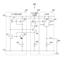
- FIG. 2 is a circuit diagram showing a configuration example of the reference voltage generation circuit 200 according to the first embodiment of the present technology.
- This reference voltage generation circuit 200 includes a PTAT current generation section 300 , a CTAT current generation section 400 and an output section 500 .
- the PTAT current generator 300 generates a PTAT current whose value changes in proportion to the absolute temperature with a positive temperature coefficient.
- This PTAT current generator 300 includes current sources 310 and 320 , bipolar transistors 331 and 332 , and a resistor 301 .
- the CTAT current generator 400 generates a CTAT current that has a negative temperature coefficient and changes in value in proportion to the absolute temperature.
- This CTAT current generator 400 comprises a current source 430 and a resistor 402 .
- the output section 500 outputs a voltage corresponding to the sum of the PTAT current and the CTAT current as the reference voltage VBGR .
- This output section 500 comprises current sources 540 and 550 and a resistor 503 .
- current sources 310 and 320 are connected in parallel to one of the power supply voltage VDD and the ground voltage VSS. In the configuration illustrated in the figure, current sources 310 and 320 are connected in parallel to power supply voltage VDD. Current sources 310, 320 and 550 form a current mirror circuit with current source 310 as a reference source. In the figure, a circuit surrounded by a constant dashed line indicates a current mirror circuit.
- Bipolar transistors 331 and 332 are of different sizes and are connected in parallel to a current mirror circuit including current sources 310 and 320 .
- the area of the bipolar transistor 332 is N (N is an integer) times that of the bipolar transistor 331 .
- bipolar transistors 331 and 332 for example, NPN type transistors are used, and their bases are connected to each other.
- One end of resistor 301 is connected to the emitter of bipolar transistor 332 .
- the emitter of bipolar transistor 331 and the other end of resistor 301 are connected to ground voltage VSS.
- the current source 430 and the resistor 402 are inserted in series between the power supply voltage VDD and the ground voltage VSS.
- a connection node of current source 430 and resistor 402 is commonly connected to the respective bases of bipolar transistors 331 and 332 .
- Current sources 430 and 540 form a current mirror circuit with current source 430 as a reference source.
- current sources 540 and 550 are connected in parallel to one of power supply voltage VDD and ground voltage VSS (power supply voltage VDD in the figure).
- One end of resistor 503 is commonly connected to current sources 540 and 550, and the other end is connected to ground voltage VSS.
- the voltage at the connection node between current sources 540 and 550 and resistor 503 is output as reference voltage VBGR .
- the current sources 310, 320, 430, 540 and 550 are examples of the first current source, the second current source, the third current source, the fourth current source and the fifth current source described in the claims.
- the resistors 301, 402 and 503 are examples of the first resistor, the second resistor and the third resistor described in the claims.
- FIG. 3 is a circuit diagram showing a specific configuration example of the reference voltage generation circuit 200 according to the first embodiment of the present technology.
- pMOS p-channel Metal Oxide Semiconductor
- transistors 311, 321, 431, 541 and 551 are used, for example. It is assumed that the pMOS transistors 311, 321 and 551 forming the current mirror circuit have the same size and a mirror ratio of one. It is also assumed that the pMOS transistors 431 and 541 forming the current mirror circuit have the same size and a mirror ratio of one.
- the pMOS transistors 311, 321, 431, 541 and 551 are examples of MOS (Metal Oxide Semiconductor) transistors described in the claims.
- the gate of pMOS transistor 311 is connected to its own drain and the gate of pMOS transistor 321 .
- the gate of pMOS transistor 431 is connected to the collector of bipolar transistor 332 .
- the gate of pMOS transistor 541 is connected to the gate of pMOS transistor 431 .
- the gate of pMOS transistor 551 is connected to the gate of pMOS transistor 311 .
- V be1 and V be2 are the base-emitter voltages of bipolar transistors 331 and 332 and V T is the thermal voltage.
- the units of these voltages are, for example, volts (V).
- k is Boltzmann's constant, and its unit is, for example, Joules per Kelvin (J/K).
- T is the absolute temperature, and the unit is, for example, Kelvin (K).
- q is the elementary charge, and its unit is, for example, coulomb (C).
- ln() is a function that returns the natural logarithm.
- PTAT current IPTAT0 ⁇ V be /R 1 Equation 2
- the unit of the PTAT current IPTAT0 is, for example, amperes (A).
- R1 is the resistance value of the resistor 301, and the unit is ohm ( ⁇ ), for example.
- a value obtained by dividing the right side of the above equation by T is a positive value.
- the pMOS transistor 431 and the resistor 402 form a source-grounded amplifier.
- the output of this source-grounded amplifier is commonly connected to the bases of bipolar transistors 331 and 332, and the gate of pMOS transistor 431 is connected to the collector of bipolar transistor 332 to form a feedback circuit.
- the base-emitter voltage V be1 of the bipolar transistor 331 is applied to the resistor 402 . Since this base-emitter voltage V be1 is generally proportional to temperature with a negative temperature coefficient, the current flowing through the resistor 402 due to this voltage is the CTAT current.
- This CTAT current I CTAT0 is expressed by the following equation.
- I CTAT0 V be1 /R 2 Equation 3
- the unit of the CTAT current I CTAT0 is, for example, amperes (A).
- R2 is the resistance value of the resistor 402, and its unit is, for example, ohms ( ⁇ ).
- a value obtained by dividing the right side of the above equation by T is a negative value.
- CTAT current I CTAT0 is duplicated and output from pMOS transistor 541 .
- output section 500 a current equal to the sum of PTAT current I PTAT0 and CTAT current I CTAT0 flows through resistor 503 .
- This current becomes a value that does not depend on the absolute temperature by making the positive and negative temperature coefficients approximately the same. Therefore, the voltage generated across the resistor 503 by the current is output as the reference voltage VBGR .
- This reference voltage V BGR is expressed by the following equation based on equations (2) and (3).
- the unit of the reference voltage VBGR is, for example, volts (V).
- R3 is the resistance value of the resistor 503, and its unit is ohm ( ⁇ ), for example.
- the positive temperature coefficient of I -PTAT0 and the negative temperature coefficient of I -CTAT0 are set substantially the same by adjusting N, R1 and R2 .
- V MIN V be1 +V dsp Equation 5
- V dsp the overdrive voltage applied between the drain and source of pMOS transistor 431 .
- the units of V MIN and V dsp are, for example, volts (V).
- the minimum operating voltage V MIN is obtained from Equation 5. is 1.2 volts (V).
- CTAT current generator 400 a circuit having a configuration in which a source follower and a resistor are connected in series is assumed as a comparative example.
- FIG. 4 is a circuit diagram showing a configuration example of a reference voltage generation circuit in a comparative example.
- the CTAT current generator 400 further includes an nMOS transistor MN.
- the pMOS transistor 321 becomes the reference source of the current mirror circuit.
- the gate of pMOS transistor 431 is connected to its own drain.
- the nMOS transistor MN is inserted between the pMOS transistor 431 and the resistor 402 and has its gate connected to the connection node between the pMOS transistor 311 and the bipolar transistor 331 . With this connection configuration, the nMOS transistor MN constitutes a source follower.
- the circuit in FIG. 5 is simplified.
- the minimum operating voltage can be lowered as compared with the case of using an operational amplifier.
- the circuit area can be reduced more than when operational amplifiers are used.
- V MIN V be1 +V dsp +V gsn Equation 6
- V gsn the threshold voltage applied between the gate and source of the nMOS transistor MN.
- the minimum operating voltage is lower than in the comparative example in which the source follower is provided in the CTAT current generator 400.
- FIG. 5 is an example of a graph showing startup characteristics with respect to the power supply voltage VDD in the first embodiment of the present technology and the comparative example.
- the vertical axis in the figure indicates the reference voltage VBGR , and the horizontal axis indicates the power supply voltage VDD.
- a solid curve indicates the starting characteristics of the first embodiment, and a dotted line indicates the starting characteristics of the comparative example.
- the comparative example uses a source follower, so the minimum operating voltage is higher than that of the first embodiment.
- the comparative example requires a minimum operating voltage of about 1.8 volts (V), while the first embodiment requires about 1.2 volts (V).
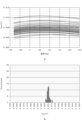
- FIG. 6 is a graph showing Monte Carlo simulation results in the first embodiment of the present technology.
- a indicates the results obtained by Monte Carlo simulation of the temperature dependence characteristics when the power supply voltage is 3 volts (V) in the first embodiment.
- b shows a histogram of the reference voltage V BGR when the temperature is 27°C.
- FIG. 7 is a graph showing Monte Carlo simulation results in a comparative example.
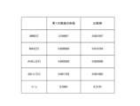
- Figure 8 summarizes the results of Figures 6 and 7.
- MIN and “MAX” in the figure indicate the minimum and maximum values of the reference voltage.
- AVE and “SD” indicate the mean and standard deviation of the reference voltage.
- MIN, MAX, AVE, SD, and ⁇ / ⁇ are the same between the first embodiment and the comparative example, but the minimum operating voltage in the first embodiment is It is 1.2 volts or the like, and can operate at a lower voltage than the comparative example with a minimum operating voltage of 1.8 volts or the like.
- FIG. 9 is a graph showing an example of power supply voltage dependence characteristics according to the first embodiment of the present technology.
- a indicates the power supply voltage dependent characteristic.
- the vertical axis of a in the figure indicates the reference voltage VBGR
- the horizontal axis indicates the power supply voltage VDD.
- a thin solid line indicates the temperature dependence under the ff condition where the thresholds of pMOS and nMOS are low.
- a thick solid line indicates the temperature dependence of the ss condition with high pMOS and nMOS thresholds.
- the dashed-dotted line indicates a tt condition in which the pMOS and nMOS thresholds are intermediate values.
- b indicates the sensitivity LS (Line Sensitivity) to the power supply line in the range from the lowest operating voltage to 3 volts (V).
- FIG. 10 is a graph showing an example of power supply voltage dependence characteristics in a comparative example.
- the minimum operating voltage can be made lower than in the comparative example under each of the ss, ff, and tt conditions.
- the dependence of the first embodiment on the DC power supply voltage is greatly improved compared to the comparative example.
- FIG. 11 is a graph showing an example of PSRR characteristics at the same power supply voltage in the first embodiment and the comparative example of the present technology.
- a shows an example of PSRR characteristics when a capacitance of 50 picofarads (pF) is added to the reference voltage generating circuit.
- b shows an example of PSRR characteristics when a 100 kilo-ohm (k ⁇ ) resistor and a low-pass filter are added to the reference voltage generating circuit.
- the vertical axis of a and b in the figure indicates PSRR, and the horizontal axis indicates frequency.
- a solid curve indicates the characteristics of the first embodiment, and a dotted line indicates the characteristics of the comparative example.
- the amplifier is of the source-grounded type, so that a high gain can be obtained from a lower power supply voltage. low and good characteristics are obtained.
- the amplifier has a high gain, deterioration of the PSRR characteristic begins at a frequency lower than that of the comparative example in a high frequency band, so measures such as installing a low-pass filter may be taken to avoid this.
- FIG. 12 is a graph showing an example of power supply voltage dependence characteristics of PSRR characteristics in a low frequency band in the first embodiment and the comparative example of the present technology.
- the vertical axis in the figure indicates PSRR, and the horizontal axis indicates power supply voltage VDD.
- the PSRR is lower than in the comparative example.
- a PNP bipolar transistor can also be used as shown in FIG.
- bipolar transistors 312, 322, 432, 542 and 552 are used instead of pMOS transistors 311, 321, 431, 541 and 551.
- the CTAT current is generated by the source-grounded pMOS transistor 431 and the resistor 402, so that the minimum operating voltage can be lowered compared to the case of using a source follower. can be done.
- the pMOS transistors 311, 321, 431, 541 and 551 used as current sources are connected to the power supply voltage VDD, but they can also be connected to the ground voltage VSS.
- the reference voltage generation circuit 200 of the second embodiment differs from that of the first embodiment in that the current source is arranged on the ground side.
- FIG. 14 is a circuit diagram showing a configuration example of the reference voltage generation circuit 200 according to the second embodiment of the present technology.
- nMOS transistors 313, 323, 433, 543 and 553 are used in place of pMOS transistors 311, 321, 431, 541 and 551, and these are grounded. placed.
- PNP bipolar transistors 333 and 334 are used instead of NPN bipolar transistors 331 and 332 .
- the reference voltage V BGR is a value obtained by subtracting R 3 (I PTAT0 +I CTAT0 ) from the power supply voltage VDD.
- the base current was assumed to be negligible.
- CMOS Complementary MOS
- parasitic bipolar transistors due to well coupling are often used, so that the current amplification factor becomes small and the influence of the base current cannot be ignored.
- the reference voltage generation circuit 200 of the third embodiment differs from that of the first embodiment in that the base current is canceled by adding a current source.
- FIG. 15 is a circuit diagram showing a configuration example of the reference voltage generation circuit 200 according to the third embodiment of the present technology.
- the reference voltage generation circuit 200 of the third embodiment differs from the first embodiment in that a pMOS transistor 561 is further arranged in the output section 500.
- FIG. 15 is a circuit diagram showing a configuration example of the reference voltage generation circuit 200 according to the third embodiment of the present technology.
- the reference voltage generation circuit 200 of the third embodiment differs from the first embodiment in that a pMOS transistor 561 is further arranged in the output section 500.
- the pMOS transistor 561 is connected in parallel with the pMOS transistors 541 and 551 between the power supply voltage VDD and the resistor 503 . It is also assumed that the pMOS transistor 561 has the same size as the pMOS transistors 311 , 321 and 551 . Also, the gate of the pMOS transistor 561 is connected to the gate of the pMOS transistor 311 . Note that the pMOS transistor 561 is an example of the sixth current source described in the claims.
- the collector current of each of the bipolar transistors 331 and 332 is ⁇ times the base current Ib , where ⁇ is the current amplification factor.
- the collector current IPTAT1 of the bipolar transistors 331 and 332 is expressed by the following equation. .
- I CTAT1 I CTAT0 +2I b Equation 8
- the term of the base current Ib remains when the current gain is small. Therefore, when the current amplification factor ⁇ increases or decreases due to variations in the process of the bipolar transistors 331 and 332, the absolute value and temperature dependency of the reference voltage VBGR greatly vary.
- the pMOS transistor 561 is added in parallel to double the mirror ratio.
- the reference voltage VBGR of the third embodiment has the value of the following equation.
- the base current Ib can be canceled.
- the temperature coefficient of I PTAT0 is set to one-half that of I CTAT0 .
- the mirror ratio of the PTAT current is doubled.
- the mirror ratio is not limited to 2x.
- the value of the mirror ratio may be set to an appropriate value according to the number of bipolar transistors.
- compensation of the base current Ib can be realized very simply and easily simply by changing the mirror ratio of the current mirror circuit, and both low voltage and small area are achieved. Is possible.
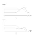
- FIG. 16 is a diagram for explaining the effects of the third embodiment of the present technology.
- a is a graph showing the temperature dependency of the reference voltage VBGR in the first embodiment when the base current remains.
- b is a graph showing the temperature dependency of the reference voltage VBGR in the third embodiment.
- the vertical axis of a and b in the figure is the reference voltage VBGR , and the horizontal axis is the absolute temperature.
- a thin solid line indicates the temperature dependence of the ss condition.
- a thick solid line indicates the temperature dependence of the ff condition.
- the dashed-dotted line indicates the tt condition.
- the addition of the pMOS transistor 561 can cancel the base current.
- variations in absolute value and temperature dependence of reference voltage V BGR can be reduced.
- the addition of the current source cancels the base current, but the addition of the resistor can also cancel the base current.
- the reference voltage generating circuit 200 in the modified example of the third embodiment differs from the third embodiment in that the base current is canceled by adding a resistor.
- FIG. 17 is a circuit diagram showing one configuration example of the reference voltage generation circuit 200 in the modified example of the third embodiment of the present technology.
- the reference voltage generation circuit 200 of the modified example of the third embodiment differs from the third embodiment in that a resistor 504 is arranged instead of the pMOS transistor 561 .
- a resistor 504 is inserted between the pMOS transistor 551 and the resistor 503 .
- a connection node of resistors 503 and 504 is connected to pMOS transistor 541, and the voltage of the connection node of pMOS transistor 551 and resistor 504 is output as reference voltage VBGR .
- the temperature coefficient of I_PTAT0 is set to 1/(1+ ⁇ ) of the temperature coefficient of I_CTAT0 .
- the resistor 504 is inserted between the pMOS transistor 551 and the resistor 503, so the base current can be cancelled.
- the reference voltage generation circuit 200 of the fourth embodiment differs from that of the first embodiment in that a circuit for detecting the base current is added to cancel the base current.
- FIG. 18 is a circuit diagram showing one configuration example of the reference voltage generation circuit 200 according to the fourth embodiment of the present technology.
- the reference voltage generation circuit 200 of the fourth embodiment differs from that of the first embodiment in that it further includes a base current detector 610 .
- the base current detection section 610 detects the base current and corrects the CTAT current based on the base current.
- the base current detector 610 includes pMOS transistors 611 to 613 , an nMOS transistor 614 and a bipolar transistor 615 .
- the pMOS transistors 611 to 613 are connected in parallel to the power supply voltage VDD.
- the drain of pMOS transistor 611 is connected to the connection node of pMOS transistor 431 and resistor 402 .
- the gate of pMOS transistor 612 is connected to its own drain and the gate of pMOS transistor 611 .
- nMOS transistor 614 is inserted between the pMOS transistor 612 and the base of the bipolar transistor 615 .
- Bipolar transistor 615 is inserted between pMOS transistor 613 and ground voltage VSS.
- the gate of nMOS transistor 614 is connected to the connection node of pMOS transistor 613 and bipolar transistor 615 .
- the pMOS transistors 611 and 612 constitute a current mirror circuit with the pMOS transistor 612 as a reference source, and the mirror ratio is set to one.
- the pMOS transistor 611 duplicates the base current Ib of the pMOS transistor 612 and supplies it to the CTAT current generator 400 . This base current Ib is added to the CTAT current ICTAT2 supplied by the pMOS transistor 431 .
- I CTAT2 is expressed by the following equation.
- the pMOS transistors 613 and 311 form a current mirror circuit with the pMOS transistor 311 as a reference source, and the mirror ratio is one.
- the pMOS transistor 613 duplicates IPTAT1 supplied from the pMOS transistor 311 and supplies it to the bipolar transistor 615 .
- the minimum operating voltage may increase due to the vertical stacking of the bipolar transistor 615 and the nMOS transistor 614, but this problem can be alleviated by using the nMOS transistor 614 with a small threshold voltage.
- the base current detection unit 610 detects the base current and corrects the CTAT current, so the base current can be canceled.
- the base current Ib is added to the CTAT current ICTAT2 , but the base current Ib can be subtracted from the current flowing through the resistor 503.
- the reference voltage generating circuit 200 in this modification of the fourth embodiment differs from the fourth embodiment in that the base current Ib is subtracted from the current flowing through the resistor 503.
- FIG. 19 is a circuit diagram showing a configuration example of the reference voltage generation circuit 200 in the modified example of the fourth embodiment of the present technology.
- Reference voltage generating circuit 200 of the modification of the fourth embodiment differs from the fourth embodiment in that nMOS transistors 616 and 617 are further provided in base current detecting portion 610 .
- the pMOS transistor 611 of the modified example of the fourth embodiment differs from the fourth embodiment in that it is not connected to the CTAT current generator 400 .
- nMOS transistor 616 is inserted between the pMOS transistor 611 and the ground voltage VSS.
- the gate of nMOS transistor 616 is connected to its drain and to the gate of nMOS transistor 617 .
- NMOS transistor 617 is inserted between the connection node of pMOS transistor 541 and resistor 503 and ground voltage VSS.
- NMOS transistors 616 and 617 form a current mirror circuit with nMOS transistor 616 as a reference source, and the mirror ratio is set to one.
- the base current Ib supplied by pMOS transistor 611 is replicated by nMOS transistor 617 . Since the nMOS transistor 617 is connected to the connection node of the pMOS transistor 541 and the resistor 503 , the base current Ib is subtracted from the current flowing through the resistor 503 . By subtracting this base current Ib , the reference voltage VBGR becomes a value represented by the following equation.
- the base current detection unit 610 detects the base current and subtracts it from the current flowing through the resistor 503, so the base current can be canceled.
- the base current detector 610 corrects the base current remaining in the sum of the PTAT current and the CTAT current in the output section 500. Instead, the base current error for only the PTAT current is You can also correct the minutes.
- the reference voltage generation circuit 200 of the fifth embodiment differs from that of the fourth embodiment in that the base current detector 610 corrects the PTAT current.
- FIG. 20 is a circuit diagram showing one configuration example of the reference voltage generation circuit 200 according to the fifth embodiment of the present technology.
- the reference voltage generation circuit 200 of the fifth embodiment differs from that of the fourth embodiment in that a pMOS transistor 618 is further provided.
- the pMOS transistor 611 of the modified example of the fifth embodiment differs from that of the fourth embodiment in that it is not connected to the CTAT current generator 400 .
- the gate of pMOS transistor 311 is also connected to the gate of pMOS transistor 618, and the source of pMOS transistor 618 is connected to power supply voltage VDD. Also, the drain of the pMOS transistor 618 is connected to the drain of the pMOS transistor 611 .
- the pMOS transistors 618 and 311 form a current mirror circuit with the pMOS transistor 311 as a reference source, and the mirror ratio is assumed to be one.
- a pMOS transistor 618 duplicates and supplies the PTAT current IPTAT1 .
- PTAT current IPTAT0 obtained by adding IPTAT1 and base current Ib (in other words, IPTAT1 is corrected by Ib ) is output to the outside.
- This PTAT current IPTAT0 is used in, for example, a temperature detection circuit such as a temperature sensor mounted on the same semiconductor integrated circuit.
- the pMOS transistors 311 and 551 form a current mirror circuit with the pMOS transistor 311 as a reference source, and the mirror ratio is doubled. By changing the mirror ratio, the base current is canceled as in the third embodiment.
- the base current detection unit 610 corrects and outputs the PTAT current IPTAT1 . can.
- the output section 500 outputs the reference voltage VBGR , but it can also output a reference current that does not depend on the absolute temperature.
- Reference voltage generating circuit 200 in the sixth embodiment differs from the sixth embodiment in that it further outputs a reference current.
- FIG. 21 is a circuit diagram showing one configuration example of the reference voltage generation circuit 200 according to the sixth embodiment of the present technology.
- Reference voltage generation circuit 200 of the sixth embodiment includes replica circuit 620 , phase compensation capacitor 630 , and pMOS transistors 561 and 571 .
- Replica circuit 620 includes pMOS transistor 621 and bipolar transistor 622 .
- Replica circuit 620 generates PTAT current IPTAT1 by a circuit equivalent to pMOS transistor 311 and bipolar transistor 331 .
- PMOS transistor 621 and bipolar transistor 622 in replica circuit 620 are connected in series between power supply voltage VDD and ground voltage VSS.
- the base of bipolar transistor 622 is connected to the base of bipolar transistor 331 .
- the drain of pMOS transistor 621 is connected to its own gate and to the gate of pMOS transistor 571 .
- pMOS transistors 561 and 571 are connected in parallel to power supply voltage VDD.
- the gate of pMOS transistor 561 is connected to the gate of pMOS transistor 431 .
- the drains of pMOS transistors 561 and 571 are connected, and a current obtained by adding the PTAT current and the CTAT current is output from the connection node as reference current IBGR .
- the phase compensation capacitor 630 is inserted between the gate of the pMOS transistor 431 and the power supply voltage VDD.
- the temperature coefficient of I - - PTAT0 is set to 1/3 that of I - - CTAT0 .
- node 701 is the gate and drain of pMOS transistor 311 and node 702 is the gate of pMOS transistor 431 .
- the PTAT current generation section 300 and the CTAT current generation section 400 are operated as two-stage operational amplifiers, and the phase compensation capacitor 630 is connected to the node 702 corresponding to the input of the CTAT current generation section 400. A primary pole is placed. Also, the node 701 of the PTAT current generator 300 becomes a node that forms the secondary pole frequency.
- a bipolar transistor 622 is added, which draws out a signal line from the node 704 of the gate of the bipolar transistor 331 and uses the bipolar transistor 331 as a reference source. Also, the replica circuit 620 extracts the PTAT current, and the gate voltage for extending the PTAT current is extracted from the node 703 of the gate of the pMOS transistor 621 .
- the impedance of node 704 is parallel to the input resistance of the base of bipolar transistor 331 and resistor 402, and is relatively low in value, so the effect on stability is low.
- the second embodiment can be applied to the sixth embodiment.
- a modification of the third embodiment can also be applied.
- the resistor 504 may be inserted between the resistor 503 and the pMOS transistor 551, or the resistor 503 may be divided.
- the fourth and fifth embodiments can be applied to the sixth embodiment.
- phase compensation capacitor 630 is inserted between the node 702 and the power supply voltage VDD in FIG. may Miller compensation can reduce the capacitance value of the phase compensation capacitor.
- PSRR characteristics are sacrificed.
- the replica circuit 620 since the replica circuit 620 is provided, it is possible to improve the stability of the circuit when expanding the output.
- the reference voltage VBGR is generated without using the phase compensation capacitor, but this configuration may cause the circuit to become unstable.
- the reference voltage generation circuit 200 in the seventh embodiment differs from the first embodiment in that a phase compensation capacitor is added.
- FIG. 22 is a circuit diagram showing one configuration example of the reference voltage generation circuit 200 according to the seventh embodiment of the present technology.
- Reference voltage generation circuit 200 of the seventh embodiment further includes pMOS transistors 341 and 351 , nMOS transistors 361 , 371 , 381 and 391 , resistor 641 and phase compensation capacitor 642 .
- the pMOS transistors 341 and 351 are connected in parallel to the power supply voltage VDD.
- PMOS transistors 341 and 311 constitute a current mirror circuit with pMOS transistor 311 as a reference source.
- PMOS transistors 351 and 321 form a current mirror circuit with pMOS transistor 321 as a reference source.
- the nMOS transistors 361 and 381 are connected in series between the pMOS transistor 341 and the ground voltage VSS.
- a connection node between the pMOS transistor 341 and the nMOS transistor 361 is connected to the CTAT current generator 400 .
- NMOS transistors 371 and 391 are connected in series between pMOS transistor 351 and ground voltage VSS.
- the gate of the nMOS transistor 371 is connected to its own drain and the gate of the nMOS transistor 361 .
- the gate of nMOS transistor 391 is connected to its own drain and the gate of nMOS transistor 381 .
- the PTAT current generator 300 constitutes a folded differential circuit.
- a resistor 641 and a phase compensation capacitor 642 are connected in series between the connection node of the cascode-connected nMOS transistors 361 and 381 and the connection node of the pMOS transistor 431 and the resistor 402 .
- connection node of the cascode-connected nMOS transistors 361 and 381 is determined with reference to the ground. The same applies to the connection node of pMOS transistor 431 and resistor 402 .
- phase compensation capacitor 642 By inserting the phase compensation capacitor 642 between these nodes, it is possible to reduce the capacitance value of the phase compensation capacitor 642 required for sufficient phase compensation as compared with the case where it is inserted at other locations. .
- resistance to power supply noise is improved, and it becomes possible to ensure both stability and maintenance of PSRR characteristics.
- phase compensation capacitor 642 is inserted between the nodes whose potential is determined based on the ground reference, it is possible to reduce the capacitance value required when performing phase compensation. can be done.
- the present technology can also have the following configuration.
- a reference voltage generation circuit comprising: an output section for outputting a reference voltage corresponding to the sum of the PTAT currents supplied by the first and second current sources and the CTAT current supplied by the third current source.
- the output unit a fourth current source that duplicates and supplies the CTAT current; a fifth current source that duplicates and supplies the PTAT current;
- the reference voltage generation circuit according to (1) further comprising a third resistor commonly connected to the fourth current source and the fifth current source.
- the first current source, the second current source, the third current source, the fourth current source, and the fifth current source are MOS (Metal Oxide Semiconductor) transistors. Voltage generation circuit.
- the first current source, the second current source, the third current source, the fourth current source and the fifth current source are connected in parallel to the power supply voltage (2) to (4). ).
- the first current source, the second current source, the third current source, the fourth current source and the fifth current source are connected in parallel to the ground voltage; ).
- the output unit further includes a sixth current source that duplicates and supplies the PTAT current;
- the reference voltage generation circuit according to any one of (2) to (6), wherein the third resistor is commonly connected to the fourth current source, the fifth current source and the sixth current source.
- the output unit further includes a fourth resistor inserted between the third resistor and the fifth current source;
- the reference voltage generation circuit according to any one of (2) to (6), wherein the fourth current source is connected to a connection node between the third resistor and the fourth resistor.
- (11) The reference voltage generation circuit according to (9), wherein the base current detector subtracts the base current from the current flowing through the third resistor.
- the PTAT current generator further comprises a pair of cascode-connected transistors, The reference voltage generation circuit according to (14), wherein a connection node of the pair of transistors is connected to the phase compensation capacitor.
- an integrated circuit A first current source and a second current source connected in parallel to one of a power supply voltage and a ground voltage, and a pair of bipolar transistors connected in parallel to a current mirror circuit including the first current source and the second current source.
- a PTAT Proportional to Absolute Temperature
- a third current source and a second resistor inserted in series between the power supply voltage and the ground voltage, wherein a connection node of the third current source and the second resistor is connected to each gate of the pair of bipolar transistors
- a CTAT Complementary to Absolute Temperature
Landscapes
- Engineering & Computer Science (AREA)
- Physics & Mathematics (AREA)
- Electromagnetism (AREA)
- General Physics & Mathematics (AREA)
- Radar, Positioning & Navigation (AREA)
- Automation & Control Theory (AREA)
- Microelectronics & Electronic Packaging (AREA)
- Power Engineering (AREA)
- Nonlinear Science (AREA)
- Control Of Electrical Variables (AREA)
Priority Applications (3)
| Application Number | Priority Date | Filing Date | Title |
|---|---|---|---|
| EP22920445.8A EP4465147A4 (en) | 2022-01-11 | 2022-11-16 | REFERENCE VOLTAGE GENERATION CIRCUIT AND ELECTRONIC DEVICE |
| JP2023573867A JPWO2023135925A1 (https=) | 2022-01-11 | 2022-11-16 | |
| US18/724,424 US20250147532A1 (en) | 2022-01-11 | 2022-11-16 | Reference voltage generation circuit and electronic device |
Applications Claiming Priority (2)
| Application Number | Priority Date | Filing Date | Title |
|---|---|---|---|
| JP2022002191 | 2022-01-11 | ||
| JP2022-002191 | 2022-01-11 |
Publications (1)
| Publication Number | Publication Date |
|---|---|
| WO2023135925A1 true WO2023135925A1 (ja) | 2023-07-20 |
Family
ID=87278858
Family Applications (1)
| Application Number | Title | Priority Date | Filing Date |
|---|---|---|---|
| PCT/JP2022/042509 Ceased WO2023135925A1 (ja) | 2022-01-11 | 2022-11-16 | 基準電圧発生回路および電子機器 |
Country Status (4)
| Country | Link |
|---|---|
| US (1) | US20250147532A1 (https=) |
| EP (1) | EP4465147A4 (https=) |
| JP (1) | JPWO2023135925A1 (https=) |
| WO (1) | WO2023135925A1 (https=) |
Cited By (3)
| Publication number | Priority date | Publication date | Assignee | Title |
|---|---|---|---|---|
| CN118012207A (zh) * | 2024-02-01 | 2024-05-10 | 深圳市亿方电子有限公司 | 一种高电源抑制比参考电压集成电路 |
| WO2025225772A1 (ko) * | 2024-04-23 | 2025-10-30 | 국립한밭대학교 산학협력단 | 양자컴퓨팅 환경을 위한 극저온 정전압 발생 회로 |
| TWI917985B (zh) | 2024-06-20 | 2026-03-11 | 瑞昱半導體股份有限公司 | 能隙電壓參考電路及電壓比較系統 |
Citations (4)
| Publication number | Priority date | Publication date | Assignee | Title |
|---|---|---|---|---|
| JP2006519433A (ja) * | 2003-02-27 | 2006-08-24 | アナログ ディヴァイスィズ インク | バンドギャップ基準電圧回路および温度曲率補正された基準電圧の生成方法 |
| JP2011186744A (ja) * | 2010-03-08 | 2011-09-22 | Fujitsu Semiconductor Ltd | バンドギャップ回路、低電圧検出回路及びレギュレータ回路 |
| CN109976425A (zh) * | 2019-04-25 | 2019-07-05 | 湖南品腾电子科技有限公司 | 一种低温度系数基准源电路 |
| US20210004031A1 (en) * | 2019-07-01 | 2021-01-07 | Stmicroelectronics S.R.I. | Low power voltage reference circuits |
Family Cites Families (6)
| Publication number | Priority date | Publication date | Assignee | Title |
|---|---|---|---|---|
| US7511567B2 (en) * | 2005-10-06 | 2009-03-31 | Avago Technologies Ecbu Ip (Singapore) Pte. Ltd. | Bandgap reference voltage circuit |
| IT1397432B1 (it) * | 2009-12-11 | 2013-01-10 | St Microelectronics Rousset | Circuito generatore di una grandezza elettrica di riferimento. |
| KR102627994B1 (ko) * | 2018-10-04 | 2024-01-22 | 삼성전자주식회사 | 비휘발성 메모리 장치의 센싱 회로, 이를 포함하는 비휘발성 메모리 장치 및 비휘발성 메모리 장치의 동작 방법 |
| EP3680745B1 (en) * | 2019-01-09 | 2022-12-21 | NXP USA, Inc. | Self-biased temperature-compensated zener reference |
| EP3683649A1 (en) * | 2019-01-21 | 2020-07-22 | NXP USA, Inc. | Bandgap current architecture optimized for size and accuracy |
| US11637534B2 (en) * | 2021-09-22 | 2023-04-25 | Texas Instruments Incorporated | Bandgap amplifier biasing and startup scheme |
-
2022
- 2022-11-16 US US18/724,424 patent/US20250147532A1/en active Pending
- 2022-11-16 EP EP22920445.8A patent/EP4465147A4/en active Pending
- 2022-11-16 WO PCT/JP2022/042509 patent/WO2023135925A1/ja not_active Ceased
- 2022-11-16 JP JP2023573867A patent/JPWO2023135925A1/ja active Pending
Patent Citations (4)
| Publication number | Priority date | Publication date | Assignee | Title |
|---|---|---|---|---|
| JP2006519433A (ja) * | 2003-02-27 | 2006-08-24 | アナログ ディヴァイスィズ インク | バンドギャップ基準電圧回路および温度曲率補正された基準電圧の生成方法 |
| JP2011186744A (ja) * | 2010-03-08 | 2011-09-22 | Fujitsu Semiconductor Ltd | バンドギャップ回路、低電圧検出回路及びレギュレータ回路 |
| CN109976425A (zh) * | 2019-04-25 | 2019-07-05 | 湖南品腾电子科技有限公司 | 一种低温度系数基准源电路 |
| US20210004031A1 (en) * | 2019-07-01 | 2021-01-07 | Stmicroelectronics S.R.I. | Low power voltage reference circuits |
Non-Patent Citations (2)
| Title |
|---|
| JUN YIN ET AL.: "A system-on-Chip EPC Gen-2 passive UHF RFID tag with embedded temperature sensor", IEEE JOURNAL OF SOLID-STATE CIRCUITS, 2010 |
| See also references of EP4465147A4 |
Cited By (3)
| Publication number | Priority date | Publication date | Assignee | Title |
|---|---|---|---|---|
| CN118012207A (zh) * | 2024-02-01 | 2024-05-10 | 深圳市亿方电子有限公司 | 一种高电源抑制比参考电压集成电路 |
| WO2025225772A1 (ko) * | 2024-04-23 | 2025-10-30 | 국립한밭대학교 산학협력단 | 양자컴퓨팅 환경을 위한 극저온 정전압 발생 회로 |
| TWI917985B (zh) | 2024-06-20 | 2026-03-11 | 瑞昱半導體股份有限公司 | 能隙電壓參考電路及電壓比較系統 |
Also Published As
| Publication number | Publication date |
|---|---|
| EP4465147A1 (en) | 2024-11-20 |
| US20250147532A1 (en) | 2025-05-08 |
| EP4465147A4 (en) | 2025-04-30 |
| JPWO2023135925A1 (https=) | 2023-07-20 |
Similar Documents
| Publication | Publication Date | Title |
|---|---|---|
| CN101657775B (zh) | 低噪声电压基准电路 | |
| US6885178B2 (en) | CMOS voltage bandgap reference with improved headroom | |
| US9454163B2 (en) | Method and device for generating an adjustable bandgap reference voltage | |
| CN100527041C (zh) | 低偏移带隙电压参考 | |
| US10671109B2 (en) | Scalable low output impedance bandgap reference with current drive capability and high-order temperature curvature compensation | |
| US4829266A (en) | CMOS power operational amplifier | |
| CN108351662B (zh) | 具有曲率补偿的带隙参考电路 | |
| JP3841195B2 (ja) | 差動増幅器 | |
| US20100148857A1 (en) | Methods and apparatus for low-voltage bias current and bias voltage generation | |
| WO2023135925A1 (ja) | 基準電圧発生回路および電子機器 | |
| Xu et al. | A novel 0.84 ppm/° C CMOS curvature-compensated bandgap with 1.2 V supply voltage | |
| Ming et al. | A high-precision compensated CMOS bandgap voltage reference without resistors | |
| CN116400768B (zh) | 带失调和噪声消除和基极电流补偿的带隙基准电压源 | |
| CN115857609A (zh) | 一种指数型温度补偿的无运放带隙基准电路 | |
| CN116736926A (zh) | 具有降噪和温度稳定性的带隙电路及其方法 | |
| US4912427A (en) | Power supply noise rejection technique for amplifiers | |
| CN115933797A (zh) | 用于产生参考电压的参考电压电路 | |
| CN114020089A (zh) | 一种适用于低电流增益型npn三极管的带隙基准电压源 | |
| CN107783584B (zh) | 和绝对温度成比例的参考电路和电压参考电路 | |
| CN112596576A (zh) | 带隙基准电路 | |
| CN118466670A (zh) | 一种带隙基准电路及其设计方法、芯片 | |
| Nischal et al. | Study of a self biased high swing cascode current mirror based folded cascode operational amplifier | |
| CN106155171A (zh) | 线性温度系数补偿的带隙电压基准电路 | |
| Wang et al. | An amplifier‐offset‐insensitive and high PSRR subthreshold CMOS voltage reference | |
| CN219016862U (zh) | 一种指数型温度补偿的无运放带隙基准电路 |
Legal Events
| Date | Code | Title | Description |
|---|---|---|---|
| 121 | Ep: the epo has been informed by wipo that ep was designated in this application |
Ref document number: 22920445 Country of ref document: EP Kind code of ref document: A1 |
|
| ENP | Entry into the national phase |
Ref document number: 2023573867 Country of ref document: JP Kind code of ref document: A |
|
| WWE | Wipo information: entry into national phase |
Ref document number: 2022920445 Country of ref document: EP |
|
| NENP | Non-entry into the national phase |
Ref country code: DE |
|
| ENP | Entry into the national phase |
Ref document number: 2022920445 Country of ref document: EP Effective date: 20240812 |
|
| WWP | Wipo information: published in national office |
Ref document number: 18724424 Country of ref document: US |