WO2023135925A1 - 基準電圧発生回路および電子機器 - Google Patents
基準電圧発生回路および電子機器 Download PDFInfo
- Publication number
- WO2023135925A1 WO2023135925A1 PCT/JP2022/042509 JP2022042509W WO2023135925A1 WO 2023135925 A1 WO2023135925 A1 WO 2023135925A1 JP 2022042509 W JP2022042509 W JP 2022042509W WO 2023135925 A1 WO2023135925 A1 WO 2023135925A1
- Authority
- WO
- WIPO (PCT)
- Prior art keywords
- current
- current source
- reference voltage
- resistor
- ptat
- Prior art date
Links
Images


Classifications
-
- G—PHYSICS
- G05—CONTROLLING; REGULATING
- G05F—SYSTEMS FOR REGULATING ELECTRIC OR MAGNETIC VARIABLES
- G05F3/00—Non-retroactive systems for regulating electric variables by using an uncontrolled element, or an uncontrolled combination of elements, such element or such combination having self-regulating properties
- G05F3/02—Regulating voltage or current
- G05F3/08—Regulating voltage or current wherein the variable is dc
- G05F3/10—Regulating voltage or current wherein the variable is dc using uncontrolled devices with non-linear characteristics
- G05F3/16—Regulating voltage or current wherein the variable is dc using uncontrolled devices with non-linear characteristics being semiconductor devices
- G05F3/20—Regulating voltage or current wherein the variable is dc using uncontrolled devices with non-linear characteristics being semiconductor devices using diode- transistor combinations
- G05F3/30—Regulators using the difference between the base-emitter voltages of two bipolar transistors operating at different current densities
Definitions
- This technology relates to a reference voltage generation circuit. More specifically, the present invention relates to a bandgap reference type reference voltage generation circuit and an electronic device.
- the bandgap reference method has been used to generate a constant voltage that does not depend on the power supply voltage or temperature.
- This bandgap reference method is classified into a voltage addition type and a current addition type.
- the voltage addition type is a method of adding a PTAT (Proportional to Absolute Temperature) voltage and a CTAT (Complementary to Absolute Temperature) voltage.
- the current addition type is a method of adding the PTAT current and the CTAT current.
- Non-Patent Document 1 a current addition type reference voltage generation circuit that generates a CTAT current in a circuit in which a drain-grounded transistor (that is, a source follower) and a resistor are connected in series to a current mirror circuit without using an operational amplifier.
- the conventional technology described above aims to lower the minimum operating voltage, reduce offset variations, and reduce the circuit area compared to using operational amplifiers.
- the reference voltage generating circuit described above it is difficult to further reduce the minimum operating voltage.
- This technology was created in view of this situation, and aims to reduce the minimum operating voltage in a circuit that generates a constant reference voltage.
- the present technology has been made to solve the above-described problems, and a first aspect thereof includes a first current source and a second current source connected in parallel to one of a power supply voltage and a ground voltage;
- a PTAT Proportional PTAT
- a PTAT Proportional PTAT comprising a pair of bipolar transistors connected in parallel to a current mirror circuit including the first current source and the second current source, and a first resistor connected to one emitter of the pair of bipolar transistors.
- a CTAT (Complementary to Absolute Temperature) current generator commonly connected to each gate of a pair of bipolar transistors, a PTAT current supplied by the first current source and the second current source, and a supply of the third current source and an output unit for outputting a reference voltage corresponding to the sum of the CTAT current and the reference voltage generation circuit. This brings about the effect of lowering the minimum operating voltage of the reference voltage generating circuit.
- the output unit includes a fourth current source that duplicates and supplies the CTAT current, a fifth current source that duplicates and supplies the PTAT current, the fourth current source, and and a third resistor commonly connected to the fifth current source.
- the first current source, the second current source, the third current source, the fourth current source, and the fifth current source are MOS (Metal Oxide Semiconductor) transistors, good too. This brings about the effect that the currents supplied by the MOS transistors are added.
- the first current source, the second current source, the third current source, the fourth current source, and the fifth current source may be bipolar transistors. This brings about the effect that the currents supplied by the bipolar transistors are added.
- the first current source, the second current source, the third current source, the fourth current source, and the fifth current source may be connected in parallel to the power supply voltage. good. This brings about the effect that the currents flowing from the current sources are added.
- the first current source, the second current source, the third current source, the fourth current source, and the fifth current source may be connected in parallel to the ground voltage. good. This brings about the effect that the currents flowing through the current sources are added.
- the output unit further includes a sixth current source that duplicates and supplies the PTAT current
- the third resistor includes the fourth current source, the fifth current source, and the It may be connected in common to the sixth current source. This brings about the effect of canceling the base current.
- the output section further includes a fourth resistor interposed between the third resistor and the fifth current source, the fourth current source comprising the third resistor and the fifth current source. It may be connected to the connection node of the fourth resistor. This brings about the effect of canceling the base current.
- a base current detection section for detecting base currents of the pair of bipolar transistors may be further provided. This brings about the effect of canceling the base current.
- the base current detection section may add the base current to the CTAT current supplied by the third current source. This brings about the effect of canceling the base current.
- the base current detection section may subtract the base current from the current flowing through the third resistor. This brings about the effect of canceling the base current.
- the base current detection section may correct the PTAT current using the base current and output the corrected PTAT current. This brings about an effect that a temperature detection circuit or the like is realized.
- the first aspect further includes a replica circuit that generates the PTAT current and supplies it to the output section, and the output section adds the PTAT current supplied by the replica circuit to the CTAT current.
- a current may be output together with the reference voltage as a reference current. This brings about the effect of avoiding deterioration of stability during output expansion.
- the PTAT current generator may include a folded differential circuit. This brings about the effect of lowering the minimum operating voltage.
- the first aspect further comprises a phase compensation capacitor inserted between the PTAT current generating section and a connection node of the third current source and the second resistor, wherein the PTAT current generating section
- a pair of cascode-connected transistors may be further provided, and a connection node of the pair of transistors may be connected to the phase compensation capacitor. This brings about the effect of improving the stability of the circuit.
- a second aspect of the present technology includes an integrated circuit, a first current source and a second current source connected in parallel to one of a power supply voltage and a ground voltage, and the first current source and the second current source.
- a PTAT (Proportional to Absolute Temperature) current generator comprising a pair of bipolar transistors connected in parallel to a current mirror circuit including a first resistor connected to one emitter of the pair of bipolar transistors; a third current source and a second resistor inserted in series between the voltage and the ground voltage, a connection node of the third current source and the second resistor being common to the respective gates of the pair of bipolar transistors;
- a CTAT Complementary to Absolute Temperature
- This has the effect of lowering the minimum operating voltage of the reference voltage generating circuit in the electronic device.
- FIG. 1 is a block diagram showing a configuration example of an electronic device according to a first embodiment of the present technology
- FIG. 1 is a circuit diagram showing a configuration example of a reference voltage generation circuit according to a first embodiment of the present technology
- FIG. 1 is a circuit diagram showing a specific configuration example of a reference voltage generation circuit according to a first embodiment of the present technology
- FIG. FIG. 4 is a circuit diagram showing a configuration example of a reference voltage generation circuit in a comparative example
- It is an example of the graph which shows the starting characteristic with respect to the power supply voltage in 1st Embodiment of this technique, and a comparative example. It is a graph which shows the Monte Carlo simulation result in a 1st embodiment of this art.
- 7 is a graph showing an example of power supply voltage dependence characteristics in a comparative example
- 7 is a graph showing an example of PSRR (Power Supply Rejection Ratio) characteristics at the same power supply voltage in the first embodiment of the present technology and a comparative example
- 7 is a graph showing an example of power supply voltage dependence characteristics of PSRR characteristics in a low frequency band in the first embodiment of the present technology and a comparative example
- It is a circuit diagram showing another example of the reference voltage generation circuit in the first embodiment of the present technology.
- It is a circuit diagram showing a configuration example of a reference voltage generation circuit according to a second embodiment of the present technology.
- It is a circuit diagram which shows one structural example of the reference voltage generation circuit in 3rd Embodiment of this technique.
- First embodiment (example of generating CTAT current with current source and resistor) 2.
- Second embodiment (an example in which a current source is placed on the ground side and a CTAT current is generated by the current source and resistor) 3.
- Third Embodiment (Example of canceling base current and generating CTAT current by current source and resistor) 4.
- Fourth embodiment (an example of detecting and canceling a base current and generating a CTAT current with a current source and a resistor) 5.
- Fifth Embodiment (Example of correcting PTAT current and generating CTAT current by current source and resistor) 6.
- Sixth Embodiment (Example of expanding output and generating CTAT current with current source and resistor) 7.
- Seventh Embodiment (Example of reducing phase compensation capacitance and generating CTAT current by current source and resistor)
- FIG. 1 is a block diagram showing a configuration example of an electronic device 100 according to the first embodiment of the present technology.
- This electronic device 100 includes a reference voltage generation circuit 200 and an integrated circuit 110 .
- the reference voltage generation circuit 200 generates a constant voltage as the reference voltage V BGR that does not depend on the power supply voltage or temperature.
- the reference voltage generation circuit 200 supplies the generated voltage to the integrated circuit 110 via the output signal line 209 .
- the integrated circuit 110 is driven by the reference voltage VBGR and executes predetermined processing such as arithmetic processing.
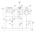
- FIG. 2 is a circuit diagram showing a configuration example of the reference voltage generation circuit 200 according to the first embodiment of the present technology.
- This reference voltage generation circuit 200 includes a PTAT current generation section 300 , a CTAT current generation section 400 and an output section 500 .
- the PTAT current generator 300 generates a PTAT current whose value changes in proportion to the absolute temperature with a positive temperature coefficient.
- This PTAT current generator 300 includes current sources 310 and 320 , bipolar transistors 331 and 332 , and a resistor 301 .
- the CTAT current generator 400 generates a CTAT current that has a negative temperature coefficient and changes in value in proportion to the absolute temperature.
- This CTAT current generator 400 comprises a current source 430 and a resistor 402 .
- the output section 500 outputs a voltage corresponding to the sum of the PTAT current and the CTAT current as the reference voltage VBGR .
- This output section 500 comprises current sources 540 and 550 and a resistor 503 .
- current sources 310 and 320 are connected in parallel to one of the power supply voltage VDD and the ground voltage VSS. In the configuration illustrated in the figure, current sources 310 and 320 are connected in parallel to power supply voltage VDD. Current sources 310, 320 and 550 form a current mirror circuit with current source 310 as a reference source. In the figure, a circuit surrounded by a constant dashed line indicates a current mirror circuit.
- Bipolar transistors 331 and 332 are of different sizes and are connected in parallel to a current mirror circuit including current sources 310 and 320 .
- the area of the bipolar transistor 332 is N (N is an integer) times that of the bipolar transistor 331 .
- bipolar transistors 331 and 332 for example, NPN type transistors are used, and their bases are connected to each other.
- One end of resistor 301 is connected to the emitter of bipolar transistor 332 .
- the emitter of bipolar transistor 331 and the other end of resistor 301 are connected to ground voltage VSS.
- the current source 430 and the resistor 402 are inserted in series between the power supply voltage VDD and the ground voltage VSS.
- a connection node of current source 430 and resistor 402 is commonly connected to the respective bases of bipolar transistors 331 and 332 .
- Current sources 430 and 540 form a current mirror circuit with current source 430 as a reference source.
- current sources 540 and 550 are connected in parallel to one of power supply voltage VDD and ground voltage VSS (power supply voltage VDD in the figure).
- One end of resistor 503 is commonly connected to current sources 540 and 550, and the other end is connected to ground voltage VSS.
- the voltage at the connection node between current sources 540 and 550 and resistor 503 is output as reference voltage VBGR .
- the current sources 310, 320, 430, 540 and 550 are examples of the first current source, the second current source, the third current source, the fourth current source and the fifth current source described in the claims.
- the resistors 301, 402 and 503 are examples of the first resistor, the second resistor and the third resistor described in the claims.
- FIG. 3 is a circuit diagram showing a specific configuration example of the reference voltage generation circuit 200 according to the first embodiment of the present technology.
- pMOS p-channel Metal Oxide Semiconductor
- transistors 311, 321, 431, 541 and 551 are used, for example. It is assumed that the pMOS transistors 311, 321 and 551 forming the current mirror circuit have the same size and a mirror ratio of one. It is also assumed that the pMOS transistors 431 and 541 forming the current mirror circuit have the same size and a mirror ratio of one.
- the pMOS transistors 311, 321, 431, 541 and 551 are examples of MOS (Metal Oxide Semiconductor) transistors described in the claims.
- the gate of pMOS transistor 311 is connected to its own drain and the gate of pMOS transistor 321 .
- the gate of pMOS transistor 431 is connected to the collector of bipolar transistor 332 .
- the gate of pMOS transistor 541 is connected to the gate of pMOS transistor 431 .
- the gate of pMOS transistor 551 is connected to the gate of pMOS transistor 311 .
- V be1 and V be2 are the base-emitter voltages of bipolar transistors 331 and 332 and V T is the thermal voltage.
- the units of these voltages are, for example, volts (V).
- k is Boltzmann's constant, and its unit is, for example, Joules per Kelvin (J/K).
- T is the absolute temperature, and the unit is, for example, Kelvin (K).
- q is the elementary charge, and its unit is, for example, coulomb (C).
- ln() is a function that returns the natural logarithm.
- PTAT current IPTAT0 ⁇ V be /R 1 Equation 2
- the unit of the PTAT current IPTAT0 is, for example, amperes (A).
- R1 is the resistance value of the resistor 301, and the unit is ohm ( ⁇ ), for example.
- a value obtained by dividing the right side of the above equation by T is a positive value.
- the pMOS transistor 431 and the resistor 402 form a source-grounded amplifier.
- the output of this source-grounded amplifier is commonly connected to the bases of bipolar transistors 331 and 332, and the gate of pMOS transistor 431 is connected to the collector of bipolar transistor 332 to form a feedback circuit.
- the base-emitter voltage V be1 of the bipolar transistor 331 is applied to the resistor 402 . Since this base-emitter voltage V be1 is generally proportional to temperature with a negative temperature coefficient, the current flowing through the resistor 402 due to this voltage is the CTAT current.
- This CTAT current I CTAT0 is expressed by the following equation.
- I CTAT0 V be1 /R 2 Equation 3
- the unit of the CTAT current I CTAT0 is, for example, amperes (A).
- R2 is the resistance value of the resistor 402, and its unit is, for example, ohms ( ⁇ ).
- a value obtained by dividing the right side of the above equation by T is a negative value.
- CTAT current I CTAT0 is duplicated and output from pMOS transistor 541 .
- output section 500 a current equal to the sum of PTAT current I PTAT0 and CTAT current I CTAT0 flows through resistor 503 .
- This current becomes a value that does not depend on the absolute temperature by making the positive and negative temperature coefficients approximately the same. Therefore, the voltage generated across the resistor 503 by the current is output as the reference voltage VBGR .
- This reference voltage V BGR is expressed by the following equation based on equations (2) and (3).
- the unit of the reference voltage VBGR is, for example, volts (V).
- R3 is the resistance value of the resistor 503, and its unit is ohm ( ⁇ ), for example.
- the positive temperature coefficient of I -PTAT0 and the negative temperature coefficient of I -CTAT0 are set substantially the same by adjusting N, R1 and R2 .
- V MIN V be1 +V dsp Equation 5
- V dsp the overdrive voltage applied between the drain and source of pMOS transistor 431 .
- the units of V MIN and V dsp are, for example, volts (V).
- the minimum operating voltage V MIN is obtained from Equation 5. is 1.2 volts (V).
- CTAT current generator 400 a circuit having a configuration in which a source follower and a resistor are connected in series is assumed as a comparative example.
- FIG. 4 is a circuit diagram showing a configuration example of a reference voltage generation circuit in a comparative example.
- the CTAT current generator 400 further includes an nMOS transistor MN.
- the pMOS transistor 321 becomes the reference source of the current mirror circuit.
- the gate of pMOS transistor 431 is connected to its own drain.
- the nMOS transistor MN is inserted between the pMOS transistor 431 and the resistor 402 and has its gate connected to the connection node between the pMOS transistor 311 and the bipolar transistor 331 . With this connection configuration, the nMOS transistor MN constitutes a source follower.
- the circuit in FIG. 5 is simplified.
- the minimum operating voltage can be lowered as compared with the case of using an operational amplifier.
- the circuit area can be reduced more than when operational amplifiers are used.
- V MIN V be1 +V dsp +V gsn Equation 6
- V gsn the threshold voltage applied between the gate and source of the nMOS transistor MN.
- the minimum operating voltage is lower than in the comparative example in which the source follower is provided in the CTAT current generator 400.
- FIG. 5 is an example of a graph showing startup characteristics with respect to the power supply voltage VDD in the first embodiment of the present technology and the comparative example.
- the vertical axis in the figure indicates the reference voltage VBGR , and the horizontal axis indicates the power supply voltage VDD.
- a solid curve indicates the starting characteristics of the first embodiment, and a dotted line indicates the starting characteristics of the comparative example.
- the comparative example uses a source follower, so the minimum operating voltage is higher than that of the first embodiment.
- the comparative example requires a minimum operating voltage of about 1.8 volts (V), while the first embodiment requires about 1.2 volts (V).
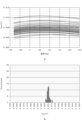
- FIG. 6 is a graph showing Monte Carlo simulation results in the first embodiment of the present technology.
- a indicates the results obtained by Monte Carlo simulation of the temperature dependence characteristics when the power supply voltage is 3 volts (V) in the first embodiment.
- b shows a histogram of the reference voltage V BGR when the temperature is 27°C.
- FIG. 7 is a graph showing Monte Carlo simulation results in a comparative example.
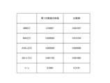
- Figure 8 summarizes the results of Figures 6 and 7.
- MIN and “MAX” in the figure indicate the minimum and maximum values of the reference voltage.
- AVE and “SD” indicate the mean and standard deviation of the reference voltage.
- MIN, MAX, AVE, SD, and ⁇ / ⁇ are the same between the first embodiment and the comparative example, but the minimum operating voltage in the first embodiment is It is 1.2 volts or the like, and can operate at a lower voltage than the comparative example with a minimum operating voltage of 1.8 volts or the like.
- FIG. 9 is a graph showing an example of power supply voltage dependence characteristics according to the first embodiment of the present technology.
- a indicates the power supply voltage dependent characteristic.
- the vertical axis of a in the figure indicates the reference voltage VBGR
- the horizontal axis indicates the power supply voltage VDD.
- a thin solid line indicates the temperature dependence under the ff condition where the thresholds of pMOS and nMOS are low.
- a thick solid line indicates the temperature dependence of the ss condition with high pMOS and nMOS thresholds.
- the dashed-dotted line indicates a tt condition in which the pMOS and nMOS thresholds are intermediate values.
- b indicates the sensitivity LS (Line Sensitivity) to the power supply line in the range from the lowest operating voltage to 3 volts (V).
- FIG. 10 is a graph showing an example of power supply voltage dependence characteristics in a comparative example.
- the minimum operating voltage can be made lower than in the comparative example under each of the ss, ff, and tt conditions.
- the dependence of the first embodiment on the DC power supply voltage is greatly improved compared to the comparative example.
- FIG. 11 is a graph showing an example of PSRR characteristics at the same power supply voltage in the first embodiment and the comparative example of the present technology.
- a shows an example of PSRR characteristics when a capacitance of 50 picofarads (pF) is added to the reference voltage generating circuit.
- b shows an example of PSRR characteristics when a 100 kilo-ohm (k ⁇ ) resistor and a low-pass filter are added to the reference voltage generating circuit.
- the vertical axis of a and b in the figure indicates PSRR, and the horizontal axis indicates frequency.
- a solid curve indicates the characteristics of the first embodiment, and a dotted line indicates the characteristics of the comparative example.
- the amplifier is of the source-grounded type, so that a high gain can be obtained from a lower power supply voltage. low and good characteristics are obtained.
- the amplifier has a high gain, deterioration of the PSRR characteristic begins at a frequency lower than that of the comparative example in a high frequency band, so measures such as installing a low-pass filter may be taken to avoid this.
- FIG. 12 is a graph showing an example of power supply voltage dependence characteristics of PSRR characteristics in a low frequency band in the first embodiment and the comparative example of the present technology.
- the vertical axis in the figure indicates PSRR, and the horizontal axis indicates power supply voltage VDD.
- the PSRR is lower than in the comparative example.
- a PNP bipolar transistor can also be used as shown in FIG.
- bipolar transistors 312, 322, 432, 542 and 552 are used instead of pMOS transistors 311, 321, 431, 541 and 551.
- the CTAT current is generated by the source-grounded pMOS transistor 431 and the resistor 402, so that the minimum operating voltage can be lowered compared to the case of using a source follower. can be done.
- the pMOS transistors 311, 321, 431, 541 and 551 used as current sources are connected to the power supply voltage VDD, but they can also be connected to the ground voltage VSS.
- the reference voltage generation circuit 200 of the second embodiment differs from that of the first embodiment in that the current source is arranged on the ground side.
- FIG. 14 is a circuit diagram showing a configuration example of the reference voltage generation circuit 200 according to the second embodiment of the present technology.
- nMOS transistors 313, 323, 433, 543 and 553 are used in place of pMOS transistors 311, 321, 431, 541 and 551, and these are grounded. placed.
- PNP bipolar transistors 333 and 334 are used instead of NPN bipolar transistors 331 and 332 .
- the reference voltage V BGR is a value obtained by subtracting R 3 (I PTAT0 +I CTAT0 ) from the power supply voltage VDD.
- the base current was assumed to be negligible.
- CMOS Complementary MOS
- parasitic bipolar transistors due to well coupling are often used, so that the current amplification factor becomes small and the influence of the base current cannot be ignored.
- the reference voltage generation circuit 200 of the third embodiment differs from that of the first embodiment in that the base current is canceled by adding a current source.
- FIG. 15 is a circuit diagram showing a configuration example of the reference voltage generation circuit 200 according to the third embodiment of the present technology.
- the reference voltage generation circuit 200 of the third embodiment differs from the first embodiment in that a pMOS transistor 561 is further arranged in the output section 500.
- the pMOS transistor 561 is connected in parallel with the pMOS transistors 541 and 551 between the power supply voltage VDD and the resistor 503 . It is also assumed that the pMOS transistor 561 has the same size as the pMOS transistors 311 , 321 and 551 . Also, the gate of the pMOS transistor 561 is connected to the gate of the pMOS transistor 311 . Note that the pMOS transistor 561 is an example of the sixth current source described in the claims.
- the collector current of each of the bipolar transistors 331 and 332 is ⁇ times the base current Ib , where ⁇ is the current amplification factor.
- the collector current IPTAT1 of the bipolar transistors 331 and 332 is expressed by the following equation. .
- I CTAT1 I CTAT0 +2I b Equation 8
- the term of the base current Ib remains when the current gain is small. Therefore, when the current amplification factor ⁇ increases or decreases due to variations in the process of the bipolar transistors 331 and 332, the absolute value and temperature dependency of the reference voltage VBGR greatly vary.
- the pMOS transistor 561 is added in parallel to double the mirror ratio.
- the reference voltage VBGR of the third embodiment has the value of the following equation.
- the base current Ib can be canceled.
- the temperature coefficient of I PTAT0 is set to one-half that of I CTAT0 .
- the mirror ratio of the PTAT current is doubled.
- the mirror ratio is not limited to 2x.
- the value of the mirror ratio may be set to an appropriate value according to the number of bipolar transistors.
- compensation of the base current Ib can be realized very simply and easily simply by changing the mirror ratio of the current mirror circuit, and both low voltage and small area are achieved. Is possible.
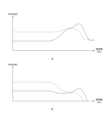
- FIG. 16 is a diagram for explaining the effects of the third embodiment of the present technology.
- a is a graph showing the temperature dependency of the reference voltage VBGR in the first embodiment when the base current remains.
- b is a graph showing the temperature dependency of the reference voltage VBGR in the third embodiment.
- the vertical axis of a and b in the figure is the reference voltage VBGR , and the horizontal axis is the absolute temperature.
- a thin solid line indicates the temperature dependence of the ss condition.
- a thick solid line indicates the temperature dependence of the ff condition.
- the dashed-dotted line indicates the tt condition.
- the addition of the pMOS transistor 561 can cancel the base current.
- variations in absolute value and temperature dependence of reference voltage V BGR can be reduced.
- the addition of the current source cancels the base current, but the addition of the resistor can also cancel the base current.
- the reference voltage generating circuit 200 in the modified example of the third embodiment differs from the third embodiment in that the base current is canceled by adding a resistor.
- FIG. 17 is a circuit diagram showing one configuration example of the reference voltage generation circuit 200 in the modified example of the third embodiment of the present technology.
- the reference voltage generation circuit 200 of the modified example of the third embodiment differs from the third embodiment in that a resistor 504 is arranged instead of the pMOS transistor 561 .
- a resistor 504 is inserted between the pMOS transistor 551 and the resistor 503 .
- a connection node of resistors 503 and 504 is connected to pMOS transistor 541, and the voltage of the connection node of pMOS transistor 551 and resistor 504 is output as reference voltage VBGR .
- the temperature coefficient of I_PTAT0 is set to 1/(1+ ⁇ ) of the temperature coefficient of I_CTAT0 .
- the resistor 504 is inserted between the pMOS transistor 551 and the resistor 503, so the base current can be cancelled.
- the reference voltage generation circuit 200 of the fourth embodiment differs from that of the first embodiment in that a circuit for detecting the base current is added to cancel the base current.
- FIG. 18 is a circuit diagram showing one configuration example of the reference voltage generation circuit 200 according to the fourth embodiment of the present technology.
- the reference voltage generation circuit 200 of the fourth embodiment differs from that of the first embodiment in that it further includes a base current detector 610 .
- the base current detection section 610 detects the base current and corrects the CTAT current based on the base current.
- the base current detector 610 includes pMOS transistors 611 to 613 , an nMOS transistor 614 and a bipolar transistor 615 .
- the pMOS transistors 611 to 613 are connected in parallel to the power supply voltage VDD.
- the drain of pMOS transistor 611 is connected to the connection node of pMOS transistor 431 and resistor 402 .
- the gate of pMOS transistor 612 is connected to its own drain and the gate of pMOS transistor 611 .
- nMOS transistor 614 is inserted between the pMOS transistor 612 and the base of the bipolar transistor 615 .
- Bipolar transistor 615 is inserted between pMOS transistor 613 and ground voltage VSS.
- the gate of nMOS transistor 614 is connected to the connection node of pMOS transistor 613 and bipolar transistor 615 .
- the pMOS transistors 611 and 612 constitute a current mirror circuit with the pMOS transistor 612 as a reference source, and the mirror ratio is set to one.
- the pMOS transistor 611 duplicates the base current Ib of the pMOS transistor 612 and supplies it to the CTAT current generator 400 . This base current Ib is added to the CTAT current ICTAT2 supplied by the pMOS transistor 431 .
- I CTAT2 is expressed by the following equation.
- the pMOS transistors 613 and 311 form a current mirror circuit with the pMOS transistor 311 as a reference source, and the mirror ratio is one.
- the pMOS transistor 613 duplicates IPTAT1 supplied from the pMOS transistor 311 and supplies it to the bipolar transistor 615 .
- the minimum operating voltage may increase due to the vertical stacking of the bipolar transistor 615 and the nMOS transistor 614, but this problem can be alleviated by using the nMOS transistor 614 with a small threshold voltage.
- the base current detection unit 610 detects the base current and corrects the CTAT current, so the base current can be canceled.
- the base current Ib is added to the CTAT current ICTAT2 , but the base current Ib can be subtracted from the current flowing through the resistor 503.
- the reference voltage generating circuit 200 in this modification of the fourth embodiment differs from the fourth embodiment in that the base current Ib is subtracted from the current flowing through the resistor 503.
- FIG. 19 is a circuit diagram showing a configuration example of the reference voltage generation circuit 200 in the modified example of the fourth embodiment of the present technology.
- Reference voltage generating circuit 200 of the modification of the fourth embodiment differs from the fourth embodiment in that nMOS transistors 616 and 617 are further provided in base current detecting portion 610 .
- the pMOS transistor 611 of the modified example of the fourth embodiment differs from the fourth embodiment in that it is not connected to the CTAT current generator 400 .
- nMOS transistor 616 is inserted between the pMOS transistor 611 and the ground voltage VSS.
- the gate of nMOS transistor 616 is connected to its drain and to the gate of nMOS transistor 617 .
- NMOS transistor 617 is inserted between the connection node of pMOS transistor 541 and resistor 503 and ground voltage VSS.
- NMOS transistors 616 and 617 form a current mirror circuit with nMOS transistor 616 as a reference source, and the mirror ratio is set to one.
- the base current Ib supplied by pMOS transistor 611 is replicated by nMOS transistor 617 . Since the nMOS transistor 617 is connected to the connection node of the pMOS transistor 541 and the resistor 503 , the base current Ib is subtracted from the current flowing through the resistor 503 . By subtracting this base current Ib , the reference voltage VBGR becomes a value represented by the following equation.
- the base current detection unit 610 detects the base current and subtracts it from the current flowing through the resistor 503, so the base current can be canceled.
- the base current detector 610 corrects the base current remaining in the sum of the PTAT current and the CTAT current in the output section 500. Instead, the base current error for only the PTAT current is You can also correct the minutes.
- the reference voltage generation circuit 200 of the fifth embodiment differs from that of the fourth embodiment in that the base current detector 610 corrects the PTAT current.
- FIG. 20 is a circuit diagram showing one configuration example of the reference voltage generation circuit 200 according to the fifth embodiment of the present technology.
- the reference voltage generation circuit 200 of the fifth embodiment differs from that of the fourth embodiment in that a pMOS transistor 618 is further provided.
- the pMOS transistor 611 of the modified example of the fifth embodiment differs from that of the fourth embodiment in that it is not connected to the CTAT current generator 400 .
- the gate of pMOS transistor 311 is also connected to the gate of pMOS transistor 618, and the source of pMOS transistor 618 is connected to power supply voltage VDD. Also, the drain of the pMOS transistor 618 is connected to the drain of the pMOS transistor 611 .
- the pMOS transistors 618 and 311 form a current mirror circuit with the pMOS transistor 311 as a reference source, and the mirror ratio is assumed to be one.
- a pMOS transistor 618 duplicates and supplies the PTAT current IPTAT1 .
- PTAT current IPTAT0 obtained by adding IPTAT1 and base current Ib (in other words, IPTAT1 is corrected by Ib ) is output to the outside.
- This PTAT current IPTAT0 is used in, for example, a temperature detection circuit such as a temperature sensor mounted on the same semiconductor integrated circuit.
- the pMOS transistors 311 and 551 form a current mirror circuit with the pMOS transistor 311 as a reference source, and the mirror ratio is doubled. By changing the mirror ratio, the base current is canceled as in the third embodiment.
- the base current detection unit 610 corrects and outputs the PTAT current IPTAT1 . can.
- the output section 500 outputs the reference voltage VBGR , but it can also output a reference current that does not depend on the absolute temperature.
- Reference voltage generating circuit 200 in the sixth embodiment differs from the sixth embodiment in that it further outputs a reference current.
- FIG. 21 is a circuit diagram showing one configuration example of the reference voltage generation circuit 200 according to the sixth embodiment of the present technology.
- Reference voltage generation circuit 200 of the sixth embodiment includes replica circuit 620 , phase compensation capacitor 630 , and pMOS transistors 561 and 571 .
- Replica circuit 620 includes pMOS transistor 621 and bipolar transistor 622 .
- Replica circuit 620 generates PTAT current IPTAT1 by a circuit equivalent to pMOS transistor 311 and bipolar transistor 331 .
- PMOS transistor 621 and bipolar transistor 622 in replica circuit 620 are connected in series between power supply voltage VDD and ground voltage VSS.
- the base of bipolar transistor 622 is connected to the base of bipolar transistor 331 .
- the drain of pMOS transistor 621 is connected to its own gate and to the gate of pMOS transistor 571 .
- pMOS transistors 561 and 571 are connected in parallel to power supply voltage VDD.
- the gate of pMOS transistor 561 is connected to the gate of pMOS transistor 431 .
- the drains of pMOS transistors 561 and 571 are connected, and a current obtained by adding the PTAT current and the CTAT current is output from the connection node as reference current IBGR .
- the phase compensation capacitor 630 is inserted between the gate of the pMOS transistor 431 and the power supply voltage VDD.
- the temperature coefficient of I - - PTAT0 is set to 1/3 that of I - - CTAT0 .
- node 701 is the gate and drain of pMOS transistor 311 and node 702 is the gate of pMOS transistor 431 .
- the PTAT current generation section 300 and the CTAT current generation section 400 are operated as two-stage operational amplifiers, and the phase compensation capacitor 630 is connected to the node 702 corresponding to the input of the CTAT current generation section 400. A primary pole is placed. Also, the node 701 of the PTAT current generator 300 becomes a node that forms the secondary pole frequency.
- a bipolar transistor 622 is added, which draws out a signal line from the node 704 of the gate of the bipolar transistor 331 and uses the bipolar transistor 331 as a reference source. Also, the replica circuit 620 extracts the PTAT current, and the gate voltage for extending the PTAT current is extracted from the node 703 of the gate of the pMOS transistor 621 .
- the impedance of node 704 is parallel to the input resistance of the base of bipolar transistor 331 and resistor 402, and is relatively low in value, so the effect on stability is low.
- the second embodiment can be applied to the sixth embodiment.
- a modification of the third embodiment can also be applied.
- the resistor 504 may be inserted between the resistor 503 and the pMOS transistor 551, or the resistor 503 may be divided.
- the fourth and fifth embodiments can be applied to the sixth embodiment.
- phase compensation capacitor 630 is inserted between the node 702 and the power supply voltage VDD in FIG. may Miller compensation can reduce the capacitance value of the phase compensation capacitor.
- PSRR characteristics are sacrificed.
- the replica circuit 620 since the replica circuit 620 is provided, it is possible to improve the stability of the circuit when expanding the output.
- the reference voltage VBGR is generated without using the phase compensation capacitor, but this configuration may cause the circuit to become unstable.
- the reference voltage generation circuit 200 in the seventh embodiment differs from the first embodiment in that a phase compensation capacitor is added.
- FIG. 22 is a circuit diagram showing one configuration example of the reference voltage generation circuit 200 according to the seventh embodiment of the present technology.
- Reference voltage generation circuit 200 of the seventh embodiment further includes pMOS transistors 341 and 351 , nMOS transistors 361 , 371 , 381 and 391 , resistor 641 and phase compensation capacitor 642 .
- the pMOS transistors 341 and 351 are connected in parallel to the power supply voltage VDD.
- PMOS transistors 341 and 311 constitute a current mirror circuit with pMOS transistor 311 as a reference source.
- PMOS transistors 351 and 321 form a current mirror circuit with pMOS transistor 321 as a reference source.
- the nMOS transistors 361 and 381 are connected in series between the pMOS transistor 341 and the ground voltage VSS.
- a connection node between the pMOS transistor 341 and the nMOS transistor 361 is connected to the CTAT current generator 400 .
- NMOS transistors 371 and 391 are connected in series between pMOS transistor 351 and ground voltage VSS.
- the gate of the nMOS transistor 371 is connected to its own drain and the gate of the nMOS transistor 361 .
- the gate of nMOS transistor 391 is connected to its own drain and the gate of nMOS transistor 381 .
- the PTAT current generator 300 constitutes a folded differential circuit.
- a resistor 641 and a phase compensation capacitor 642 are connected in series between the connection node of the cascode-connected nMOS transistors 361 and 381 and the connection node of the pMOS transistor 431 and the resistor 402 .
- connection node of the cascode-connected nMOS transistors 361 and 381 is determined with reference to the ground. The same applies to the connection node of pMOS transistor 431 and resistor 402 .
- phase compensation capacitor 642 By inserting the phase compensation capacitor 642 between these nodes, it is possible to reduce the capacitance value of the phase compensation capacitor 642 required for sufficient phase compensation as compared with the case where it is inserted at other locations. .
- resistance to power supply noise is improved, and it becomes possible to ensure both stability and maintenance of PSRR characteristics.
- phase compensation capacitor 642 is inserted between the nodes whose potential is determined based on the ground reference, it is possible to reduce the capacitance value required when performing phase compensation. can be done.
- the present technology can also have the following configuration.
- a reference voltage generation circuit comprising: an output section for outputting a reference voltage corresponding to the sum of the PTAT currents supplied by the first and second current sources and the CTAT current supplied by the third current source.
- the output unit a fourth current source that duplicates and supplies the CTAT current; a fifth current source that duplicates and supplies the PTAT current;
- the reference voltage generation circuit according to (1) further comprising a third resistor commonly connected to the fourth current source and the fifth current source.
- the first current source, the second current source, the third current source, the fourth current source, and the fifth current source are MOS (Metal Oxide Semiconductor) transistors. Voltage generation circuit.
- the first current source, the second current source, the third current source, the fourth current source and the fifth current source are connected in parallel to the power supply voltage (2) to (4). ).
- the first current source, the second current source, the third current source, the fourth current source and the fifth current source are connected in parallel to the ground voltage; ).
- the output unit further includes a sixth current source that duplicates and supplies the PTAT current;
- the reference voltage generation circuit according to any one of (2) to (6), wherein the third resistor is commonly connected to the fourth current source, the fifth current source and the sixth current source.
- the output unit further includes a fourth resistor inserted between the third resistor and the fifth current source;
- the reference voltage generation circuit according to any one of (2) to (6), wherein the fourth current source is connected to a connection node between the third resistor and the fourth resistor.
- (11) The reference voltage generation circuit according to (9), wherein the base current detector subtracts the base current from the current flowing through the third resistor.
- the PTAT current generator further comprises a pair of cascode-connected transistors, The reference voltage generation circuit according to (14), wherein a connection node of the pair of transistors is connected to the phase compensation capacitor.
- an integrated circuit A first current source and a second current source connected in parallel to one of a power supply voltage and a ground voltage, and a pair of bipolar transistors connected in parallel to a current mirror circuit including the first current source and the second current source.
- a PTAT Proportional to Absolute Temperature
- a third current source and a second resistor inserted in series between the power supply voltage and the ground voltage, wherein a connection node of the third current source and the second resistor is connected to each gate of the pair of bipolar transistors
- a CTAT Complementary to Absolute Temperature
Landscapes
- Engineering & Computer Science (AREA)
- Microelectronics & Electronic Packaging (AREA)
- Physics & Mathematics (AREA)
- Power Engineering (AREA)
- Nonlinear Science (AREA)
- Electromagnetism (AREA)
- General Physics & Mathematics (AREA)
- Radar, Positioning & Navigation (AREA)
- Automation & Control Theory (AREA)
- Control Of Electrical Variables (AREA)
Abstract
一定の基準電圧を生成する回路において、最低動作電圧を低減する。 PTAT電流生成部は、電源電圧および接地電圧の一方に並列に接続された第1電流源および第2電流源と、第1電流源および第2電流源を含むカレントミラー回路に並列に接続された一対のバイポーラトランジスタと、一対のバイポーラトランジスタの一方のエミッタに接続された第1抵抗とを備える。CTAT電流生成部は、電源電圧および接地電圧の間に直列に挿入された第3電流源および第2抵抗を備える。第3電流源および第2抵抗の接続ノードが一対のバイポーラトランジスタのそれぞれのゲートに共通に接続される。出力部は、第1電流源および第2電流源の供給するPTAT電流と第3電流源の供給するCTAT電流との加算値に応じた基準電圧を出力する。
Description
本技術は、基準電圧発生回路に関する。詳しくは、バンドギャップリファレンス方式の基準電圧発生回路および電子機器に関する。
従来より、電源電圧や温度に依存しない一定の電圧を生成するために、バンドギャップリファレンス方式が用いられている。このバンドギャップリファレンス方式は、電圧加算型と電流加算型とに分類される。これらのうち電圧加算型は、PTAT(Proportional to Absolute Temperature)電圧とCTAT(Complementary to Absolute Temperature)電圧とを加算する方式である。一方、電流加算型は、PTAT電流とCTAT電流とを加算する方式である。例えば、オペアンプを用いず、ドレイン接地のトランジスタ(すなわち、ソースフォロワ)と抵抗とをカレントミラー回路に直列に接続した回路でCTAT電流を生成する電流加算型の基準電圧発生回路が提案されている(例えば、非特許文献1参照。)。
Jun Yin, et al., A system-on-Chip EPC Gen-2 passive UHF RFID tag with embedded temperature sensor, IEEE JOURNAL OF SOLID-STATE CIRCUITS, 2010.
上述の従来技術では、オペアンプの削減により、オペアンプを用いる場合と比較して、最低動作電圧の低下、オフセットばらつきの低減や、回路面積の削減を図っている。しかしながら、上述の基準電圧発生回路では、最低動作電圧をさらに低減することが困難である。
本技術はこのような状況に鑑みて生み出されたものであり、一定の基準電圧を生成する回路において、最低動作電圧を低減することを目的とする。
本技術は、上述の問題点を解消するためになされたものであり、その第1の側面は、電源電圧および接地電圧の一方に並列に接続された第1電流源および第2電流源と、上記第1電流源および上記第2電流源を含むカレントミラー回路に並列に接続された一対のバイポーラトランジスタと、上記一対のバイポーラトランジスタの一方のエミッタに接続された第1抵抗とを備えるPTAT(Proportional to Absolute Temperature)電流生成部と、上記電源電圧および上記接地電圧の間に直列に挿入された第3電流源および第2抵抗を備え、上記第3電流源および上記第2抵抗の接続ノードが上記一対のバイポーラトランジスタのそれぞれのゲートに共通に接続されたCTAT(Complementary to Absolute Temperature)電流生成部と、上記第1電流源および上記第2電流源の供給するPTAT電流と上記第3電流源の供給するCTAT電流との加算値に応じた基準電圧を出力する出力部とを具備する基準電圧発生回路である。これにより、基準電圧発生回路の最低動作電圧が低下するという作用をもたらす。
また、この第1の側面において、上記出力部は、上記CTAT電流を複製して供給する第4電流源と、上記PTAT電流を複製して供給する第5電流源と、上記第4電流源および上記第5電流源に共通に接続された第3抵抗とを備えてもよい。これにより、電流の加算値に抵抗値を乗算した値の基準電圧が生成されるという作用をもたらす。
また、この第1の側面において、上記第1電流源、上記第2電流源、上記第3電流源、上記第4電流源および上記第5電流源は、MOS(Metal Oxide Semiconductor)トランジスタであってもよい。これにより、MOSトランジスタの供給する電流が加算されるという作用をもたらす。
また、この第1の側面において、上記第1電流源、上記第2電流源、上記第3電流源、上記第4電流源および上記第5電流源は、バイポーラトランジスタであってもよい。これにより、バイポーラトランジスタの供給する電流が加算されるという作用をもたらす。
また、この第1の側面において、上記第1電流源、上記第2電流源、上記第3電流源、上記第4電流源および上記第5電流源は、上記電源電圧に並列に接続されてもよい。これにより、電流源から流れる電流が加算されるという作用をもたらす。
また、この第1の側面において、上記第1電流源、上記第2電流源、上記第3電流源、上記第4電流源および上記第5電流源は、上記接地電圧に並列に接続されてもよい。これにより、電流源に流れる電流が加算されるという作用をもたらす。
また、この第1の側面において、上記出力部は、上記PTAT電流を複製して供給する第6電流源をさらに備え、上記第3抵抗は、上記第4電流源、上記第5電流源および上記第6電流源に共通に接続されてもよい。これにより、ベース電流がキャンセルされるという作用をもたらす。
また、この第1の側面において、上記出力部は、上記第3抵抗と上記第5電流源との間に挿入された第4抵抗をさらに含み、上記第4電流源は、上記第3抵抗および上記第4抵抗の接続ノードに接続されてもよい。これにより、ベース電流がキャンセルされるという作用をもたらす。
また、この第1の側面において、上記一対のバイポーラトランジスタのベース電流を検出するベース電流検出部をさらに具備してもよい。これにより、ベース電流がキャンセルされるという作用をもたらす。
また、この第1の側面において、上記ベース電流検出部は、上記第3電流源の供給する上記CTAT電流に上記ベース電流を加算してもよい。これにより、ベース電流がキャンセルされるという作用をもたらす。
また、この第1の側面において、上記ベース電流検出部は、上記第3抵抗に流れる電流から上記ベース電流を減算してもよい。これにより、ベース電流がキャンセルされるという作用をもたらす。
また、この第1の側面において、上記ベース電流検出部は、上記ベース電流により上記PTAT電流を補正して出力してもよい。これにより、温度検出回路などが実現されるという作用をもたらす。
また、この第1の側面において、上記PTAT電流を生成して上記出力部に供給するレプリカ回路をさらに具備し、上記出力部は、上記レプリカ回路の供給する上記PTAT電流を上記CTAT電流に加算した電流を基準電流として上記基準電圧とともに出力してもよい。これにより、出力拡張時に安定性の悪化を回避できるという作用をもたらす。
また、この第1の側面において、上記PTAT電流生成部は、折り返し型の差動回路を含むものであってもよい。これにより、最低動作電圧が低下するという作用をもたらす。
また、この第1の側面において、上記PTAT電流生成部と上記第3電流源および上記第2抵抗の接続ノードとの間に挿入された位相補償容量をさらに具備し、上記PTAT電流生成部は、カスコード接続された一対のトランジスタをさらに備え、上記一対のトランジスタの接続ノードが上記位相補償容量に接続されてもよい。これにより、回路の安定性が向上するという作用をもたらす。
また、本技術の第2の側面は、集積回路と、電源電圧および接地電圧の一方に並列に接続された第1電流源および第2電流源と、上記第1電流源および上記第2電流源を含むカレントミラー回路に並列に接続された一対のバイポーラトランジスタと、上記一対のバイポーラトランジスタの一方のエミッタに接続された第1抵抗とを備えるPTAT(Proportional to Absolute Temperature)電流生成部と、上記電源電圧および上記接地電圧の間に直列に挿入された第3電流源および第2抵抗を含み、上記第3電流源および上記第2抵抗の接続ノードが上記一対のバイポーラトランジスタのそれぞれのゲートに共通に接続されたCTAT(Complementary to Absolute Temperature)電流生成部と、上記第1電流源および上記第2電流源の供給するPTAT電流と上記第3電流源の供給するCTAT電流との加算値に応じた基準電圧を上記集積回路に出力する出力部とを具備する電子機器である。これにより、電子装置内の基準電圧発生回路の最低動作電圧が低下するという作用をもたらす。
以下、本技術を実施するための形態(以下、実施の形態と称する)について説明する。説明は以下の順序により行う。
1.第1の実施の形態(電流源および抵抗によりCTAT電流を生成する例)
2.第2の実施の形態(電流源を接地側に配置し、電流源および抵抗によりCTAT電流を生成する例)
3.第3の実施の形態(ベース電流をキャンセルし、電流源および抵抗によりCTAT電流を生成する例)
4.第4の実施の形態(ベース電流を検出してキャンセルし、電流源および抵抗によりCTAT電流を生成する例)
5.第5の実施の形態(PTAT電流を補正し、電流源および抵抗によりCTAT電流を生成する例)
6.第6の実施の形態(出力を拡張し、電流源および抵抗によりCTAT電流を生成する例)
7.第7の実施の形態(位相補償容量を削減し、電流源および抵抗によりCTAT電流を生成する例)
<1.第1の実施の形態>
[電子機器の構成例]
図1は、本技術の第1の実施の形態における電子機器100の一構成例を示すブロック図である。この電子機器100は、基準電圧発生回路200および集積回路110を備える。
[電子機器の構成例]
図1は、本技術の第1の実施の形態における電子機器100の一構成例を示すブロック図である。この電子機器100は、基準電圧発生回路200および集積回路110を備える。
基準電圧発生回路200は、電源電圧や温度に依存しない一定の電圧を基準電圧VBGRとして生成するものである。この基準電圧発生回路200は、生成した電圧を、出力信号線209を介して集積回路110に供給する。集積回路110は、基準電圧VBGRにより駆動し、演算処理などの所定の処理を実行するものである。
[基準電圧発生回路の構成例]
図2は、本技術の第1の実施の形態における基準電圧発生回路200の一構成例を示す回路図である。この基準電圧発生回路200は、PTAT電流生成部300、CTAT電流生成部400および出力部500を備える。
図2は、本技術の第1の実施の形態における基準電圧発生回路200の一構成例を示す回路図である。この基準電圧発生回路200は、PTAT電流生成部300、CTAT電流生成部400および出力部500を備える。
PTAT電流生成部300は、正の温度係数をもって絶対温度に比例して値が変化するPTAT電流を生成するものである。このPTAT電流生成部300は、電流源310および320と、バイポーラトランジスタ331および332と、抵抗301とを備える。
CTAT電流生成部400は、負の温度係数をもって絶対温度に比例して値が変化するCTAT電流を生成するものである。このCTAT電流生成部400は、電流源430および抵抗402を備える。
出力部500は、PTAT電流およびCTAT電流の加算値に応じた電圧を基準電圧VBGRとして出力するものである。この出力部500は、電流源540および550と、抵抗503とを備える。
PTAT電流生成部300において、電流源310および320は、電源電圧VDDおよび接地電圧VSSの一方に並列に接続される。同図に例示した構成では、電流源310および320は、電源電圧VDDに並列に接続されている。また、電流源310、320および550は、電流源310を参照元とするカレントミラー回路を構成する。同図において、一定鎖線で囲まれた回路は、カレントミラー回路を示す。
バイポーラトランジスタ331および332は、サイズが異なり、電流源310および320を含むカレントミラー回路に並列に接続される。例えば、バイポーラトランジスタ332の面積は、バイポーラトランジスタ331のN(Nは、整数)倍とする。バイポーラトランジスタ331および332として、例えば、NPN型が用いられ、それぞれのベースは互いに接続される。抵抗301の一端は、バイポーラトランジスタ332のエミッタに接続される。バイポーラトランジスタ331のエミッタと抵抗301の他端とは、接地電圧VSSに接続される。
また、CTAT電流生成部400において、電流源430および抵抗402は、電源電圧VDDおよび接地電圧VSSの間に直列に挿入される。また、電流源430および抵抗402の接続ノードは、バイポーラトランジスタ331および332のそれぞれのベースに共通に接続される。また、電流源430および540は、電流源430を参照元とするカレントミラー回路を構成する。
また、出力部500において、電流源540および550は、電源電圧VDDおよび接地電圧VSSの一方(同図においては電源電圧VDD)に並列に接続される。抵抗503の一端は、電流源540および550に共通に接続され、他端は、接地電圧VSSに接続される。電流源540および550と抵抗503との接続ノードの電圧が基準電圧VBGRとして出力される。
なお、電流源310、320、430、540および550は、特許請求の範囲に記載の第1電流源、第2電流源、第3電流源、第4電流源および第5電流源の一例である。また、抵抗301、402および503は、特許請求の範囲に記載の第1抵抗、第2抵抗および第3抵抗の一例である。
図3は、本技術の第1の実施の形態における基準電圧発生回路200の具体的な構成例を示す回路図である。電流源310、320、430、540および550として、例えば、pMOS(p-channel Metal Oxide Semiconductor)トランジスタ311、321、431、541および551が用いられる。カレントミラー回路を構成するpMOSトランジスタ311、321および551のサイズは同一であり、ミラー比は1倍であるものとする。また、カレントミラー回路を構成するpMOSトランジスタ431および541のサイズは同一であり、ミラー比は1倍であるものとする。なお、pMOSトランジスタ311、321、431、541および551は、特許請求の範囲に記載のMOS(Metal Oxide Semiconductor)トランジスタの一例である。
pMOSトランジスタ311のゲートは、自身のドレインとpMOSトランジスタ321のゲートとに接続される。pMOSトランジスタ431のゲートは、バイポーラトランジスタ332のコレクタに接続される。pMOSトランジスタ541のゲートは、pMOSトランジスタ431のゲートに接続される。pMOSトランジスタ551のゲートは、pMOSトランジスタ311のゲートに接続される。
前述したようにバイポーラトランジスタ331および332のエミッタ面積が異なるため、それらのベース-エミッタ間電圧に差が生じる。この差電圧ΔVbeは、例えば、次の式により表される。
ΔVbe=Vbe1-Vbe2=VTln(N)
=(kT/q)ln(N) ・・・式1
上式において、Vbe1およびVbe2は、バイポーラトランジスタ331および332のベース-エミッタ間電圧であり、VTは、熱電圧である。これらの電圧の単位は、例えば、ボルト(V)である。kは、ボルツマン定数であり、単位は、例えば、ジュール毎ケルビン(J/K)である。Tは絶対温度であり、単位は、例えば、ケルビン(K)である。qは電気素量であり、単位は、例えば、クーロン(C)である。ln()は、自然対数を返す関数である。
ΔVbe=Vbe1-Vbe2=VTln(N)
=(kT/q)ln(N) ・・・式1
上式において、Vbe1およびVbe2は、バイポーラトランジスタ331および332のベース-エミッタ間電圧であり、VTは、熱電圧である。これらの電圧の単位は、例えば、ボルト(V)である。kは、ボルツマン定数であり、単位は、例えば、ジュール毎ケルビン(J/K)である。Tは絶対温度であり、単位は、例えば、ケルビン(K)である。qは電気素量であり、単位は、例えば、クーロン(C)である。ln()は、自然対数を返す関数である。
差電圧ΔVbeにより、抵抗301に流れる電流は、式1より絶対温度に比例し、PTAT電流となる。このPTAT電流IPTAT0は、次の式により表される。
IPTAT0=ΔVbe/R1 ・・・式2
上式において、PTAT電流IPTAT0の単位は、例えば、アンペア(A)である。R1は、抵抗301の抵抗値であり、単位は、例えば、オーム(Ω)である。上式の右辺をTで割った値(言い換えれば、温度係数)は、正の値となる。
IPTAT0=ΔVbe/R1 ・・・式2
上式において、PTAT電流IPTAT0の単位は、例えば、アンペア(A)である。R1は、抵抗301の抵抗値であり、単位は、例えば、オーム(Ω)である。上式の右辺をTで割った値(言い換えれば、温度係数)は、正の値となる。
ここで、同図においては、バイポーラトランジスタ331および332の電流増幅率は十分に大きく、そのベース電流を無視することができるものとする。上述のPTAT電流IPTAT0は複製され、pMOSトランジスタ551から出力される。
また、CTAT電流生成部400において、pMOSトランジスタ431および抵抗402は、ソース接地増幅器を構成する。このソース接地増幅器の出力は、バイポーラトランジスタ331および332のベースに共通に接続され、pMOSトランジスタ431のゲートはバイポーラトランジスタ332のコレクタに接続されて、帰還回路を構成する。このとき、負帰還が成立するため、抵抗402には、バイポーラトランジスタ331のベース-エミッタ間電圧Vbe1が印加される。このベース-エミッタ間電圧Vbe1は、一般に温度に対し、負の温度係数で比例するため、その電圧により抵抗402に流れる電流は、CTAT電流となる。このCTAT電流ICTAT0は、次の式により表される。
ICTAT0=Vbe1/R2 ・・・式3
上式において、CTAT電流ICTAT0の単位は、例えば、アンペア(A)である。R2は、抵抗402の抵抗値であり、単位は、例えば、オーム(Ω)である。上式の右辺をTで割った値(言い換えれば、温度係数)は、負の値となる。
ICTAT0=Vbe1/R2 ・・・式3
上式において、CTAT電流ICTAT0の単位は、例えば、アンペア(A)である。R2は、抵抗402の抵抗値であり、単位は、例えば、オーム(Ω)である。上式の右辺をTで割った値(言い換えれば、温度係数)は、負の値となる。
上述のCTAT電流ICTAT0は複製され、pMOSトランジスタ541から出力される。出力部500において、抵抗503にPTAT電流IPTAT0およびCTAT電流ICTAT0の加算値の電流が流れる。この電流は、正、負のそれぞれの温度係数を略同一にすることによって絶対温度に依存しない値となる。このため、その電流により抵抗503に生じる電圧は、基準電圧VBGRとして出力される。この基準電圧VBGRは、式2および式3に基づいて、次の式により表される。
VBGR=R3(IPTAT0+ICTAT0)
=R3{(ΔVbe/R1)+(Vbe1/R2)} ・・・式4
上式において、基準電圧VBGRの単位は、例えば、ボルト(V)である。R3は、抵抗503の抵抗値であり、単位は、例えば、オーム(Ω)である。IPTAT0の正の温度係数と、ICTAT0の負の温度係数とは、N、R1やR2の調整などにより、略同一に設定される。
VBGR=R3(IPTAT0+ICTAT0)
=R3{(ΔVbe/R1)+(Vbe1/R2)} ・・・式4
上式において、基準電圧VBGRの単位は、例えば、ボルト(V)である。R3は、抵抗503の抵抗値であり、単位は、例えば、オーム(Ω)である。IPTAT0の正の温度係数と、ICTAT0の負の温度係数とは、N、R1やR2の調整などにより、略同一に設定される。
同図に例示したように、CTAT電流生成部400内にソース接地増幅器を設け、帰還制御と、CTAT電流の生成とを同時に行うため、最低動作電圧VMINは、次の式により表される。
VMIN=Vbe1+Vdsp ・・・式5
上式において、Vdspは、pMOSトランジスタ431のドレイン-ソース間に印加されるオーバードライブ電圧を示す。VMINおよびVdspの単位は、例えば、ボルト(V)である。
VMIN=Vbe1+Vdsp ・・・式5
上式において、Vdspは、pMOSトランジスタ431のドレイン-ソース間に印加されるオーバードライブ電圧を示す。VMINおよびVdspの単位は、例えば、ボルト(V)である。
所定の電圧、温度の条件下のベース-エミッタ間電圧Vbe1を0.8ボルト(V)とし、オーバードライブ電圧Vdspを0.4ボルト(V)とすると、式5より最低動作電圧VMINは1.2ボルト(V)となる。
ここで、CTAT電流生成部400において、ソースフォロワおよび抵抗を直列に接続した構成の回路を比較例として想定する。
図4は、比較例における基準電圧発生回路の一構成例を示す回路図である。この比較例では、CTAT電流生成部400内にnMOSトランジスタMNがさらに配置される。また、pMOSトランジスタ321がカレントミラー回路の参照元になる。pMOSトランジスタ431のゲートは、自身のドレインに接続される。nMOSトランジスタMNは、pMOSトランジスタ431と抵抗402との間に挿入され、そのゲートは、pMOSトランジスタ311およびバイポーラトランジスタ331の接続ノードに接続される。この接続構成により、nMOSトランジスタMNは、ソースフォロワを構成する。同図の回路は、非特許文献1のFig.5の回路を簡易化したものである。
第1の実施の形態と比較例との両方ともオペアンプを用いていない。このため、オペアンプを用いる場合と比較して、最低動作電圧を低下させることができる。また、第1の実施の形態と比較例との両方とも、オペアンプのオフセットばらつきを考慮する必要がなくなり、さらにオペアンプを用いる場合よりも回路面積を削減することができる。ただし、CTAT電流生成部400内にソースフォロワを設けた比較例では、最低動作電圧VMINは、次の式により表される。
VMIN=Vbe1+Vdsp+Vgsn ・・・式6
上式において、Vgsnは、nMOSトランジスタMNのゲート-ソース間に印加される閾値電圧を示す。
VMIN=Vbe1+Vdsp+Vgsn ・・・式6
上式において、Vgsnは、nMOSトランジスタMNのゲート-ソース間に印加される閾値電圧を示す。
式5および式6より、CTAT電流生成部400内にソース接地増幅器を設けた第1の実施の形態では、CTAT電流生成部400内にソースフォロワを設けた比較例よりも最低動作電圧が低くなる。
図5は、本技術の第1の実施の形態と比較例とにおける電源電圧VDDに対する起動特性を示すグラフの一例である。同図における縦軸は、基準電圧VBGRを示し、横軸は、電源電圧VDDを示す。また、実線の曲線は、第1の実施の形態の起動特性を示し、点線は、比較例の起動特性を示す。
同図に例示するように、比較例では、ソースフォロワを用いているため、第1の実施の形態よりも最低動作電圧が高くなってしまう。例えば、比較例では、最低動作電圧として1.8ボルト(V)程度を要するのに対し、第1の実施の形態では、1.2ボルト(V)程度でよい。
図6は、本技術の第1の実施の形態におけるモンテカルロシミュレーション結果を示すグラフである。同図におけるaは、第1の実施の形態における電源電圧が3ボルト(V)の際の温度依存特性をモンテカルロシミュレーションにより求めた結果を示す。同図におけるbは、温度が27℃の際の基準電圧VBGRのヒストグラムを示す。
図7は、比較例におけるモンテカルロシミュレーション結果を示すグラフである。
図8は、図6および図7の結果をまとめたものである。同図における「MIN」および「MAX」は、基準電圧の最小値および最大値を示す。「AVE」および「SD」は、基準電圧の平均値および標準偏差を示す。
図5から図8に示したように、第1の実施の形態と比較例とではMIN、MAX、AVE、SD、σ/μは同等であるが、第1の実施の形態では最低動作電圧が1.2ボルトなどであり、最低動作電圧が1.8ボルトなどの比較例よりも低電圧で動作可能である。
図9は、本技術の第1の実施の形態における電源電圧依存特性の一例を示すグラフである。同図におけるaは、電源電圧依存特性を示す。また、同図におけるaの縦軸は、基準電圧VBGRを示し、横軸は、電源電圧VDDを示す。細い実線は、pMOSおよびnMOSの閾値が低いff条件の温度依存特性を示す。太い実線は、pMOSおよびnMOSの閾値が高いss条件の温度依存特性を示す。一点鎖線は、pMOSおよびnMOSの閾値が中間値のtt条件を示す。同図におけるbは、最低動作電圧から3ボルト(V)までの範囲で、電源ラインに対する感度LS(Line Sensitivity)を示す。
図10は、比較例における電源電圧依存特性の一例を示すグラフである。
図9および図10に例示したように、第1の実施の形態では、ss、ff、tt条件のそれぞれで比較例よりも最低動作電圧を低くすることができる。また、第1の実施の形態の直流的な電源電圧に対する依存性は、比較例と比較して、大幅に改善されている。
図11は、本技術の第1の実施の形態と比較例とにおける、同一電源電圧でのPSRR特性の一例を示すグラフである。同図におけるaは、基準電圧発生回路に50ピコファラッド(pF)の容量を付加したときのPSRR特性の一例を示す。同図におけるbは、基準電圧発生回路に100キロオーム(kΩ)の抵抗とローパスフィルタとを付与したときのPSRR特性の一例を示す。同図におけるaおよびbの縦軸はPSRRを示し、横軸は周波数を示す。また、実線の曲線は、第1の実施の形態の特性を示し、点線は、比較例の特性を示す。
同図に例示するように、第1の実施の形態では、増幅器をソース接地型とすることで、より低い電源電圧から高いゲインを得ることができるため、低周波数帯域のPSRRは、比較例より低く、良好な特性が得られている。一方、高いゲインを持つ反面、高周波数帯域では、PSRR特性の悪化が、比較例より低い周波数から始まるため、ローパスフィルタを設置するなどの対策で回避してもよい。
図12は、本技術の第1の実施の形態と比較例とにおける、低周波数帯域でのPSRR特性の電源電圧依存特性の一例を示すグラフである。同図の縦軸は、PSRRを示し、横軸は電源電圧VDDを示す。同図に例示するように、第1の実施の形態では、比較例よりもPSRRが低くなる。
なお、電流源310などの電流源としてpMOSトランジスタを用いているが、図13に例示するようにPNP型のバイポーラトランジスタを用いることもできる。この場合にはpMOSトランジスタ311、321、431、541および551の代わりに、バイポーラトランジスタ312、322、432、542および552が用いられる。
このように、本技術の第1の実施の形態によれば、ソース接地のpMOSトランジスタ431および抵抗402によりCTAT電流を生成するため、ソースフォロワを用いる場合と比較して最低動作電圧を低下させることができる。
<2.第2の実施の形態>
上述の第1の実施の形態では、電流源として用いられるpMOSトランジスタ311、321、431、541および551を電源電圧VDDに接続していたが、これらを接地電圧VSSに接続することもできる。この第2の実施の形態の基準電圧発生回路200は、電流源を接地側に配置した点において第1の実施の形態と異なる。
上述の第1の実施の形態では、電流源として用いられるpMOSトランジスタ311、321、431、541および551を電源電圧VDDに接続していたが、これらを接地電圧VSSに接続することもできる。この第2の実施の形態の基準電圧発生回路200は、電流源を接地側に配置した点において第1の実施の形態と異なる。
図14は、本技術の第2の実施の形態における基準電圧発生回路200の一構成例を示す回路図である。この第2の実施の形態の基準電圧発生回路200では、pMOSトランジスタ311、321、431、541および551の代わりに、nMOSトランジスタ313、323、433、543および553が用いられ、これらは接地側に配置される。また、NPN型のバイポーラトランジスタ331および332の代わりに、PNP型のバイポーラトランジスタ333および334が用いられる。基準電圧VBGRは、電源電圧VDDから、R3(IPTAT0+ICTAT0)を減算した値となる。
このように、本技術の第2の実施の形態によれば、nMOSトランジスタ313、323、433、543および553の電流源を接地側に配置したため、電源電圧VDDから、R3(IPTAT0+ICTAT0)を減算した値の基準電圧を供給することができる。
<3.第3の実施の形態>
上述の第1の実施の形態では、ベース電流が無視できるものとしていた。しかし、近年の微細化CMOS(Complementary MOS)プロセスではウェル結合による寄生バイポーラトランジスタを用いることが多いため、電流増幅率が小さくなり、ベース電流の影響を無視することができなくなることがある。この第3の実施の形態の基準電圧発生回路200は、電流源の追加によりベース電流をキャンセルした点において第1の実施の形態と異なる。
上述の第1の実施の形態では、ベース電流が無視できるものとしていた。しかし、近年の微細化CMOS(Complementary MOS)プロセスではウェル結合による寄生バイポーラトランジスタを用いることが多いため、電流増幅率が小さくなり、ベース電流の影響を無視することができなくなることがある。この第3の実施の形態の基準電圧発生回路200は、電流源の追加によりベース電流をキャンセルした点において第1の実施の形態と異なる。
図15は、本技術の第3の実施の形態における基準電圧発生回路200の一構成例を示す回路図である。この第3の実施の形態の基準電圧発生回路200は、出力部500内にpMOSトランジスタ561をさらに配置した点において第1の実施の形態と異なる。
pMOSトランジスタ561は、電源電圧VDDと抵抗503との間において、pMOSトランジスタ541および551と並列に接続される。また、pMOSトランジスタ561のサイズは、pMOSトランジスタ311、321および551と同一であるものとする。また、pMOSトランジスタ561のゲートはpMOSトランジスタ311のゲートに接続される。なお、pMOSトランジスタ561は、特許請求の範囲に記載の第6電流源の一例である。
PTAT電流生成部300において、バイポーラトランジスタ331および332のそれぞれについて、電流増幅率をβとすると、コレクタ電流は、ベース電流Ibのβ倍である。バイポーラトランジスタ331および332のそれぞれのベース電流が略一致する場合、抵抗301に流れる電流をIPTAT0とすると、バイポーラトランジスタ331および332のそれぞれのコレクタ電流であるIPTAT1は、次の式により表される。
IPTAT1=β×Ib
=IPTAT0―Ib ・・・式7
IPTAT1=β×Ib
=IPTAT0―Ib ・・・式7
次に、CTAT電流生成部400においては、バイポーラトランジスタ331および332のそれぞれのベース電流を加算した電流が流れる。このため、pMOSトランジスタの供給する電流をICTAT1とし、抵抗402に流れる電流をICTAT0とすると、ICTAT1は、次の式により表される。
ICTAT1=ICTAT0+2Ib ・・・式8
ICTAT1=ICTAT0+2Ib ・・・式8
これらのPTAT電流IPTAT1およびCTAT電流ICTAT1を1倍のミラー比で取り出すと、pMOSトランジスタ561の無い第1の実施の形態の場合、基準電圧VBGRは、式7および式8に基づいて次の式により表される。
VBGR=R3(IPTAT1+ICTAT1)
=R3(IPTAT0+ICTAT0+Ib) ・・・式9
VBGR=R3(IPTAT1+ICTAT1)
=R3(IPTAT0+ICTAT0+Ib) ・・・式9
式9に例示するように、第1の実施の形態では、電流増幅率が小さい場合、ベース電流Ibの項が残留する。このため、バイポーラトランジスタ331や332のプロセスのばらつきにより電流増幅率βが増減すると、基準電圧VBGRの絶対値と温度依存性とが大きく変動することになる。
そこで、第3の実施の形態では、pMOSトランジスタ561を並列に追加して、ミラー比を2倍にしている。これにより、第3の実施の形態の基準電圧VBGRは、次の式の値となる。
VBGR=R3(2×IPTAT1+ICTAT1)
=R3(2×IPTAT0+ICTAT0) ・・・式10
VBGR=R3(2×IPTAT1+ICTAT1)
=R3(2×IPTAT0+ICTAT0) ・・・式10
式10より、ベース電流Ibをキャンセルすることができる。IPTAT0の温度係数は、ICTAT0の温度係数の1/2に設定される。
ここでは、CTAT電流生成部400の出力に接続されるバイポーラトランジスタが2個であるために、PTAT電流のミラー比を2倍としている。しかし、ミラー比は2倍に限定されない。ミラー比の値は、バイポーラトランジスタの個数に応じて、適切な値に設定すればよい。
上述のように第3の実施の形態では、カレントミラー回路のミラー比を変更するのみでベース電流Ibの補償を非常にシンプルかつ容易に実現でき、低電圧化と小面積化とを両立することが可能である。
図16は、本技術の第3の実施の形態における効果を説明するための図である。同図におけるaは、ベース電流が残留する際の第1の実施の形態における基準電圧VBGRの温度依存特性を示すグラフである。同図におけるbは、第3の実施の形態における基準電圧VBGRの温度依存特性を示すグラフである。同図におけるaおよびbの縦軸は、基準電圧VBGRであり、横軸は絶対温度である。細い実線は、ss条件の温度依存特性を示す。太い実線は、ff条件の温度依存特性を示す。一点鎖線は、tt条件を示す。
同図におけるaおよびbに例示するように、第3の実施の形態では、第1の実施の形態と比較して、プロセスの絶対ばらつきに対して基準電圧VBGRの絶対値の変動と、基準電圧VBGRの温度依存性の変動とを低減することができる。
なお、第3の実施の形態に第2の実施の形態を適用することができる。
このように、本技術の第3の実施の形態によれば、pMOSトランジスタ561を追加したため、ベース電流をキャンセルすることができる。これにより、基準電圧VBGRの絶対値および温度依存性の変動を低減することができる。
[変形例]
上述の第3の実施の形態では、電流源の追加によりベース電流をキャンセルしていたが、抵抗の追加によりベース電流をキャンセルすることもできる。この第3の実施の形態の変形例における基準電圧発生回路200は、抵抗の追加によりベース電流をキャンセルした点において第3の実施の形態と異なる。
上述の第3の実施の形態では、電流源の追加によりベース電流をキャンセルしていたが、抵抗の追加によりベース電流をキャンセルすることもできる。この第3の実施の形態の変形例における基準電圧発生回路200は、抵抗の追加によりベース電流をキャンセルした点において第3の実施の形態と異なる。
図17は、本技術の第3の実施の形態の変形例における基準電圧発生回路200の一構成例を示す回路図である。この第3の実施の形態の変形例の基準電圧発生回路200は、pMOSトランジスタ561の代わりに、抵抗504を配置した点において第3の実施の形態と異なる。
抵抗504は、pMOSトランジスタ551と抵抗503との間に挿入される。また、抵抗503および504の接続ノードがpMOSトランジスタ541に接続され、pMOSトランジスタ551および抵抗504の接続ノードの電圧が基準電圧VBGRとして出力される。
抵抗504の抵抗値をR3×α(αは、整数)とした場合、基準電圧VBGRは、次の式により表される。
VBGR=R3×(IPTAT1+ICTAT1)+R3×α×IPTAT1
=R3×(IPTAT0+ICTAT0+Ib)
+R3×α×(IPTAT0―Ib)
=R3×{(1+α)IPTAT0+ICTAT0)}
+R3×(1-α)Ib ・・・式11
VBGR=R3×(IPTAT1+ICTAT1)+R3×α×IPTAT1
=R3×(IPTAT0+ICTAT0+Ib)
+R3×α×(IPTAT0―Ib)
=R3×{(1+α)IPTAT0+ICTAT0)}
+R3×(1-α)Ib ・・・式11
式11に基づいてαを1に設定することにより、ベース電流をキャンセルすることができる。IPTAT0の温度係数は、ICTAT0の温度係数の1/(1+α)に設定される。
ただし、この方法では、抵抗504に決められた抵抗比率αを持たせるため、トリミング機能の実装がしにくいことに留意する必要がある。
なお、第3の実施の形態の変形例に第2の実施の形態を適用することができる。
このように、本技術の第3の実施の形態の変形例によれば、pMOSトランジスタ551と抵抗503との間に抵抗504を挿入したため、ベース電流をキャンセルすることができる。
<4.第4の実施の形態>
上述の第1の実施の形態では、ベース電流が無視できるものとしていた。しかし、近年の微細化CMOSプロセスでは電流増幅率が小さくなり、ベース電流の影響を無視することができなくなることがある。この第4の実施の形態の基準電圧発生回路200は、ベース電流を検出する回路の追加によりベース電流をキャンセルした点において第1の実施の形態と異なる。
上述の第1の実施の形態では、ベース電流が無視できるものとしていた。しかし、近年の微細化CMOSプロセスでは電流増幅率が小さくなり、ベース電流の影響を無視することができなくなることがある。この第4の実施の形態の基準電圧発生回路200は、ベース電流を検出する回路の追加によりベース電流をキャンセルした点において第1の実施の形態と異なる。
図18は、本技術の第4の実施の形態における基準電圧発生回路200の一構成例を示す回路図である。この第4の実施の形態の基準電圧発生回路200は、ベース電流検出部610をさらに備える点において第1の実施の形態と異なる。
ベース電流検出部610は、ベース電流を検出し、そのベース電流によりCTAT電流を補正するものである。このベース電流検出部610は、pMOSトランジスタ611乃至613と、nMOSトランジスタ614と、バイポーラトランジスタ615とを備える。
pMOSトランジスタ611乃至613は、電源電圧VDDに並列に接続される。pMOSトランジスタ611のドレインは、pMOSトランジスタ431および抵抗402の接続ノードに接続される。pMOSトランジスタ612のゲートは、自身のドレインとpMOSトランジスタ611のゲートとに接続される。
nMOSトランジスタ614は、pMOSトランジスタ612とバイポーラトランジスタ615のベースとの間に挿入される。バイポーラトランジスタ615は、pMOSトランジスタ613と接地電圧VSSとの間に挿入される。また、nMOSトランジスタ614のゲートは、pMOSトランジスタ613およびバイポーラトランジスタ615の接続ノードに接続される。
pMOSトランジスタ611および612は、pMOSトランジスタ612を参照元とするカレントミラー回路を構成し、ミラー比は1倍とする。pMOSトランジスタ611は、pMOSトランジスタ612のベース電流Ibを複製し、CTAT電流生成部400に供給する。このベース電流Ibは、pMOSトランジスタ431の供給するCTAT電流ICTAT2に加算される。式8に基づいてICTAT2は、次の式により表される。
ICTAT2=ICTAT1-Ib
=ICTAT0+Ib ・・・式12
ICTAT2=ICTAT1-Ib
=ICTAT0+Ib ・・・式12
また、pMOSトランジスタ613および311は、pMOSトランジスタ311を参照元とするカレントミラー回路を構成し、ミラー比は1倍である。pMOSトランジスタ613は、pMOSトランジスタ311の供給するIPTAT1を複製してバイポーラトランジスタ615に供給する。
出力部500は、PTAT電流IPTAT1およびCTAT電流ICTAT2を加算する。このため、基準電圧VBGRは、式7および式12に基づいて次の式により表される。
VBGR=R3(IPTAT1+ICTAT2)
=R3(IPTAT0+ICTAT0) ・・・式13
VBGR=R3(IPTAT1+ICTAT2)
=R3(IPTAT0+ICTAT0) ・・・式13
式13より、ベース電流をキャンセルすることができる。
同図の回路では、バイポーラトランジスタ615およびnMOSトランジスタ614の縦積みにより、最低動作電圧が上昇するおそれがあるが、閾値電圧の小さいnMOSトランジスタ614を用いることにより、この問題を緩和することができる。
なお、第4の実施の形態に第2の実施の形態を適用することができる。
このように、本技術の第4の実施の形態によれば、ベース電流検出部610がベース電流を検出してCTAT電流を補正するため、ベース電流をキャンセルすることができる。
[変形例]
上述の第4の実施の形態では、CTAT電流ICTAT2にベース電流Ibを加算していたが、抵抗503に流れる電流からベース電流Ibを減算することもできる。この第4の実施の形態の変形例における基準電圧発生回路200は、抵抗503に流れる電流からベース電流Ibを減算する点において第4の実施の形態と異なる。
上述の第4の実施の形態では、CTAT電流ICTAT2にベース電流Ibを加算していたが、抵抗503に流れる電流からベース電流Ibを減算することもできる。この第4の実施の形態の変形例における基準電圧発生回路200は、抵抗503に流れる電流からベース電流Ibを減算する点において第4の実施の形態と異なる。
図19は、本技術の第4の実施の形態の変形例における基準電圧発生回路200の一構成例を示す回路図である。この第4の実施の形態の変形例の基準電圧発生回路200は、ベース電流検出部610内にnMOSトランジスタ616および617をさらに設けた点において第4の実施の形態と異なる。また、第4の実施の形態の変形例のpMOSトランジスタ611は、CTAT電流生成部400に接続されない点において第4の実施の形態と異なる。
nMOSトランジスタ616は、pMOSトランジスタ611と接地電圧VSSとの間に挿入される。nMOSトランジスタ616のゲートは、自身のドレインと、nMOSトランジスタ617のゲートとに接続される。nMOSトランジスタ617は、pMOSトランジスタ541および抵抗503の接続ノードと、接地電圧VSSとの間に挿入される。
nMOSトランジスタ616および617は、nMOSトランジスタ616を参照元とするカレントミラー回路を構成し、そのミラー比は1倍とする。pMOSトランジスタ611の供給するベース電流Ibは、nMOSトランジスタ617により複製される。このnMOSトランジスタ617は、pMOSトランジスタ541および抵抗503の接続ノードに接続されているため、抵抗503に流れる電流からベース電流Ibが減算される。このベース電流Ibの減算により、基準電圧VBGRは、次の式により表される値となる。
VBGR=R3(IPTAT1+ICTAT1-Ib)
=R3(IPTAT0+ICTAT0) ・・・式14
VBGR=R3(IPTAT1+ICTAT1-Ib)
=R3(IPTAT0+ICTAT0) ・・・式14
式14より、ベース電流をキャンセルすることができる。
なお、第4の実施の形態の変形例に第2の実施の形態を適用することができる。
このように、本技術の第4の実施の形態によれば、ベース電流検出部610がベース電流を検出して抵抗503に流れる電流から減算するため、ベース電流をキャンセルすることができる。
<5.第5の実施の形態>
上述の第4の実施の形態では、ベース電流検出部610が、出力部500におけるPTAT電流とCTAT電流の和に残留するベース電流を補正していたが、その代わりにPTAT電流のみに対するベース電流誤差分を補正することもできる。この第5の実施の形態における基準電圧発生回路200は、ベース電流検出部610がPTAT電流を補正する点において第4の実施の形態と異なる。
上述の第4の実施の形態では、ベース電流検出部610が、出力部500におけるPTAT電流とCTAT電流の和に残留するベース電流を補正していたが、その代わりにPTAT電流のみに対するベース電流誤差分を補正することもできる。この第5の実施の形態における基準電圧発生回路200は、ベース電流検出部610がPTAT電流を補正する点において第4の実施の形態と異なる。
図20は、本技術の第5の実施の形態における基準電圧発生回路200の一構成例を示す回路図である。この第5の実施の形態の基準電圧発生回路200は、pMOSトランジスタ618をさらに備える点において第4の実施の形態と異なる。また、第5の実施の形態の変形例のpMOSトランジスタ611は、CTAT電流生成部400に接続されない点において第4の実施の形態と異なる。
pMOSトランジスタ311のゲートは、pMOSトランジスタ618のゲートにも接続され、pMOSトランジスタ618のソースは電源電圧VDDに接続される。また、pMOSトランジスタ618のドレインは、pMOSトランジスタ611のドレインに接続される。
pMOSトランジスタ618および311は、pMOSトランジスタ311を参照元とするカレントミラー回路を構成し、ミラー比は1倍であるものとする。pMOSトランジスタ618は、PTAT電流IPTAT1を複製して供給する。pMOSトランジスタ611および618の接続ノードからは、IPTAT1とベース電流Ibとを加算(言い換えれば、IPTAT1をIbにより補正)したPTAT電流IPTAT0が外部に出力される。このPTAT電流IPTAT0は、例えば、同一の半導体集積回路上に温度センサーなどの温度検出回路を搭載する際に、その回路で用いられる。
また、pMOSトランジスタ311および551は、pMOSトランジスタ311を参照元とするカレントミラー回路を構成し、ミラー比は2倍とする。ミラー比の変更により、第3の実施の形態と同様にベース電流がキャンセルされる。
なお、第5の実施の形態に第2の実施の形態を適用することができる。
このように、本技術の第5の実施の形態によれば、ベース電流検出部610が、PTAT電流IPTAT1を補正して出力するため、その電流を用いて温度検出回路などを実現することができる。
<6.第6の実施の形態>
上述の第1の実施の形態では、出力部500は、基準電圧VBGRを出力していたが、絶対温度に依存しない基準電流をさらに出力することもできる。この第6の実施の形態における基準電圧発生回路200は、基準電流をさらに出力する点において第6の実施の形態と異なる。
上述の第1の実施の形態では、出力部500は、基準電圧VBGRを出力していたが、絶対温度に依存しない基準電流をさらに出力することもできる。この第6の実施の形態における基準電圧発生回路200は、基準電流をさらに出力する点において第6の実施の形態と異なる。
図21は、本技術の第6の実施の形態における基準電圧発生回路200の一構成例を示す回路図である。この第6の実施の形態の基準電圧発生回路200は、レプリカ回路620および位相補償容量630と、pMOSトランジスタ561および571とを備える。レプリカ回路620は、pMOSトランジスタ621およびバイポーラトランジスタ622を備える。
レプリカ回路620は、pMOSトランジスタ311およびバイポーラトランジスタ331と同等の回路によりPTAT電流IPTAT1を生成するものである。レプリカ回路620内のpMOSトランジスタ621およびバイポーラトランジスタ622は、電源電圧VDDと、接地電圧VSSとの間において、直列に接続される。バイポーラトランジスタ622のベースは、バイポーラトランジスタ331のベースに接続される。pMOSトランジスタ621のドレインは、自身のゲートと、pMOSトランジスタ571のゲートとに接続される。
また、出力部500において、pMOSトランジスタ561および571は、電源電圧VDDに並列に接続される。pMOSトランジスタ561のゲートは、pMOSトランジスタ431のゲートに接続される。pMOSトランジスタ561および571のドレインは、接続され、その接続ノードからは、PTAT電流およびCTAT電流を加算した電流が基準電流IBGRとして出力される。
位相補償容量630は、pMOSトランジスタ431のゲートと電源電圧VDDとの間に挿入される。
また、バイポーラトランジスタ622にもベース電流が流れるため、CTAT電流生成部400の生成するCTAT電流ICTAT3は、次の式により表される。
ICTAT3=ICTAT0+3Ib ・・・式15
ICTAT3=ICTAT0+3Ib ・・・式15
式15のベース電流をキャンセルするために、pMOSトランジスタ311および551を含むカレントミラー回路のミラー比は、3倍に設定される。このため、基準電圧VBGRは、次の式により表される値となる。
VBGR=R3(3IPTAT1+ICTAT3)
=R3(3IPTAT0+ICTAT0) ・・・式16
上式において、IPTAT0の温度係数は、ICTAT0の温度係数の1/3に設定される。
VBGR=R3(3IPTAT1+ICTAT3)
=R3(3IPTAT0+ICTAT0) ・・・式16
上式において、IPTAT0の温度係数は、ICTAT0の温度係数の1/3に設定される。
出力を拡張する場合、同図のようにレプリカ回路620を設けず、カレントミラー回路内のノード701および702から信号線を引き出してpMOSトランジスタを出力部500内に増設する方法もある。ここでノード701は、pMOSトランジスタ311のゲートおよびドレインであり、ノード702は、pMOSトランジスタ431のゲートである。
ただし、基準電圧発生回路200では、PTAT電流生成部300およびCTAT電流生成部400を2段のオペアンプとして動作させており、CTAT電流生成部400の入力にあたるノード702に位相補償容量630を接続して1次ポールを配置している。また、PTAT電流生成部300のノード701は2次ポール周波数を形成するノードとなる。
このため、レプリカ回路620が無いと、出力を拡張する際にノード701に対してゲート接続を追加することとなり、容量負荷が重くなって回路の安定性に影響する。ノード702の位相補償容量630の容量値を大きくして、帯域を低下させることで対応は可能であるが、回路面積へのインパクトが大きい。これは、低電圧動作を実現することの代償であるが、同図に例示するようにレプリカ回路620の追加により容易に回避可能である。
同図では、バイポーラトランジスタ331のゲートのノード704から信号線を引き出してバイポーラトランジスタ331を参照元とするバイポーラトランジスタ622を追加している。また、レプリカ回路620によりPTAT電流を引き出し、pMOSトランジスタ621のゲートのノード703から、PTAT電流拡張のためのゲート電圧を取り出す構成をとっている。
この構成において、ノード704のインピーダンスは、バイポーラトランジスタ331のベースの入力抵抗および抵抗402の並列となり、比較的その値が低いため、安定性への影響度は低い。
なお、第6の実施の形態に第2の実施の形態を適用することができる。また、第3の実施の形態の変形例を適用することもできる。この場合には、抵抗503とpMOSトランジスタ551との間に抵抗504を挿入するか、抵抗503を分割すればよい。また、第6の実施の形態に第4、第5の実施の形態を適用することもできる。
また、同図では、位相補償容量630をノード702と電源電圧VDDとの間に挿入しているが、2つの位相補償容量の一方をノード702に、他方をノード704に接続するミラー補償を用いてもよい。ミラー補償により、位相補償容量の容量値を削減することができる。ただし、この場合は、PSRR特性を犠牲にすることとなる点に留意する。
このように、本技術の第6の実施の形態によれば、レプリカ回路620を設けたため、出力を拡張する際に回路の安定性を向上させることができる。
<7.第7の実施の形態>
上述の第1の実施の形態では、位相補償容量を用いずに基準電圧VBGRを生成していたが、この構成では回路が不安定になるおそれがある。この第7の実施の形態における基準電圧発生回路200は、位相補償容量を追加した点において第1の実施の形態と異なる。
上述の第1の実施の形態では、位相補償容量を用いずに基準電圧VBGRを生成していたが、この構成では回路が不安定になるおそれがある。この第7の実施の形態における基準電圧発生回路200は、位相補償容量を追加した点において第1の実施の形態と異なる。
図22は、本技術の第7の実施の形態における基準電圧発生回路200の一構成例を示す回路図である。この第7の実施の形態の基準電圧発生回路200は、pMOSトランジスタ341および351と、nMOSトランジスタ361、371、381および391と、抵抗641および位相補償容量642とをさらに備える。
pMOSトランジスタ341および351は、電源電圧VDDに並列に接続される。pMOSトランジスタ341および311は、pMOSトランジスタ311を参照元とするカレントミラー回路を構成する。pMOSトランジスタ351および321は、pMOSトランジスタ321を参照元とするカレントミラー回路を構成する。
nMOSトランジスタ361および381は、pMOSトランジスタ341と接地電圧VSSとの間に直列に接続される。pMOSトランジスタ341およびnMOSトランジスタ361の接続ノードは、CTAT電流生成部400に接続される。nMOSトランジスタ371および391は、pMOSトランジスタ351と接地電圧VSSとの間に直列に接続される。また、nMOSトランジスタ371のゲートは、自身のドレインとnMOSトランジスタ361のゲートとに接続される。nMOSトランジスタ391のゲートは、自身のドレインとnMOSトランジスタ381のゲートとに接続される。
pMOSトランジスタ341および351と、nMOSトランジスタ361、371、381および391との追加により、PTAT電流生成部300は、折り返し型の差動回路を構成する。
抵抗641および位相補償容量642は、カスコード接続されたnMOSトランジスタ361および381の接続ノードと、pMOSトランジスタ431および抵抗402の接続ノードとの間において、直列に接続される。
カスコード接続されたnMOSトランジスタ361および381の接続ノードは、グランド基準で電位が決定される。pMOSトランジスタ431および抵抗402の接続ノードについても同様である。これらのノード間に位相補償容量642を挿入することにより、他の箇所に挿入する場合と比較して、十分な位相補償を行う際に必要な位相補償容量642の容量値を削減することができる。また、電源ノイズに対する耐性が向上し、安定性確保とPSRR特性維持との両立が可能となる。ただし、最低動作電圧の上昇やばらつきが生じ、ノイズが増大するおそれがあるため、設計仕様に応じ、トレードオフを見極めて設計を最適化する必要がある。
なお、第7の実施の形態に第2から第6の実施の形態のそれぞれを適用することができる。
このように、本技術の第7の実施の形態によれば、グランド基準で電位が決定されるノード間に位相補償容量642を挿入したため、位相補償を行う際に必要な容量値を削減することができる。
なお、上述の実施の形態は本技術を具現化するための一例を示したものであり、実施の形態における事項と、特許請求の範囲における発明特定事項とはそれぞれ対応関係を有する。同様に、特許請求の範囲における発明特定事項と、これと同一名称を付した本技術の実施の形態における事項とはそれぞれ対応関係を有する。ただし、本技術は実施の形態に限定されるものではなく、その要旨を逸脱しない範囲において実施の形態に種々の変形を施すことにより具現化することができる。
なお、本明細書に記載された効果はあくまで例示であって、限定されるものではなく、また、他の効果があってもよい。
なお、本技術は以下のような構成もとることができる。
(1)電源電圧および接地電圧の一方に並列に接続された第1電流源および第2電流源と、前記第1電流源および前記第2電流源を含むカレントミラー回路に並列に接続された一対のバイポーラトランジスタと、前記一対のバイポーラトランジスタの一方のエミッタに接続された第1抵抗とを備えるPTAT(Proportional to Absolute Temperature)電流生成部と、
前記電源電圧および前記接地電圧の間に直列に挿入された第3電流源および第2抵抗を備え、前記第3電流源および前記第2抵抗の接続ノードが前記一対のバイポーラトランジスタのそれぞれのゲートに共通に接続されたCTAT(Complementary to Absolute Temperature)電流生成部と、
前記第1電流源および前記第2電流源の供給するPTAT電流と前記第3電流源の供給するCTAT電流との加算値に応じた基準電圧を出力する出力部と
を具備する基準電圧発生回路。
(2)前記出力部は、
前記CTAT電流を複製して供給する第4電流源と、
前記PTAT電流を複製して供給する第5電流源と、
前記第4電流源および前記第5電流源に共通に接続された第3抵抗と
を備える前記(1)記載の基準電圧発生回路。
(3)前記第1電流源、前記第2電流源、前記第3電流源、前記第4電流源および前記第5電流源は、MOS(Metal Oxide Semiconductor)トランジスタである
前記(2)記載の基準電圧発生回路。
(4)前記第1電流源、前記第2電流源、前記第3電流源、前記第4電流源および前記第5電流源は、バイポーラトランジスタである
前記(2)記載の基準電圧発生回路。
(5)前記第1電流源、前記第2電流源、前記第3電流源、前記第4電流源および前記第5電流源は、前記電源電圧に並列に接続される
前記(2)から(4)のいずれかに記載の基準電圧発生回路。
(6)前記第1電流源、前記第2電流源、前記第3電流源、前記第4電流源および前記第5電流源は、前記接地電圧に並列に接続される
前記(2)から(4)のいずれかに記載の基準電圧発生回路。
(7)前記出力部は、前記PTAT電流を複製して供給する第6電流源をさらに備え、
前記第3抵抗は、前記第4電流源、前記第5電流源および前記第6電流源に共通に接続される
前記(2)から(6)のいずれかに記載の基準電圧発生回路。
(8)前記出力部は、前記第3抵抗と前記第5電流源との間に挿入された第4抵抗をさらに含み、
前記第4電流源は、前記第3抵抗および前記第4抵抗の接続ノードに接続される
前記(2)から(6)のいずれかに記載の基準電圧発生回路。
(9)前記一対のバイポーラトランジスタのベース電流を検出するベース電流検出部をさらに具備する
前記(2)から(8)のいずれかに記載の基準電圧発生回路。
(10)前記ベース電流検出部は、前記第3電流源の供給する前記CTAT電流に前記ベース電流を加算する
前記(9)記載の基準電圧発生回路。
(11)前記ベース電流検出部は、前記第3抵抗に流れる電流から前記ベース電流を減算する
前記(9)記載の基準電圧発生回路。
(12)前記ベース電流検出部は、前記ベース電流により前記PTAT電流を補正して出力する
前記(9)記載の基準電圧発生回路。
(13)前記PTAT電流を生成して前記出力部に供給するレプリカ回路をさらに具備し、
前記出力部は、上記レプリカ回路の供給する上記PTAT電流を前記CTAT電流に加算した電流を基準電流として前記基準電圧とともに出力する
前記(1)から(12)のいずれかに記載の基準電圧発生回路。
(14)前記PTAT電流生成部は、折り返し型の差動回路を含む
前記(1)から(13)のいずれかに記載の基準電圧生成回路。
(15)前記PTAT電流生成部と前記第3電流源および前記第2抵抗の接続ノードとの間に挿入された位相補償容量をさらに具備し、
前記PTAT電流生成部は、カスコード接続された一対のトランジスタをさらに備え、
前記一対のトランジスタの接続ノードが前記位相補償容量に接続される
前記(14)記載の基準電圧生成回路。
(16)集積回路と、
電源電圧および接地電圧の一方に並列に接続された第1電流源および第2電流源と、前記第1電流源および前記第2電流源を含むカレントミラー回路に並列に接続された一対のバイポーラトランジスタと、前記一対のバイポーラトランジスタの一方のエミッタに接続された第1抵抗とを備えるPTAT(Proportional to Absolute Temperature)電流生成部と、
前記電源電圧および前記接地電圧の間に直列に挿入された第3電流源および第2抵抗を含み、前記第3電流源および前記第2抵抗の接続ノードが前記一対のバイポーラトランジスタのそれぞれのゲートに共通に接続されたCTAT(Complementary to Absolute Temperature)電流生成部と、
前記第1電流源および前記第2電流源の供給するPTAT電流と前記第3電流源の供給するCTAT電流との加算値に応じた基準電圧を前記集積回路に出力する出力部と
を具備する電子機器。
100 電子機器
110 集積回路
200 基準電圧発生回路
300 PTAT電流生成部
301、402、503、504、641 抵抗
310、320、430、540、550 電流源
311、321、341、351、431、541、551、561、571、611~613、618、621 pMOSトランジスタ
312、322、331~334、432、542、552、615、622 バイポーラトランジスタ
313、323、361、371、381、391、433、543、553、614、616、617 nMOSトランジスタ
400 CTAT電流生成部
500 出力部
610 ベース電流検出部
620 レプリカ回路
630、642 位相補償容量
Claims (16)
- 電源電圧および接地電圧の一方に並列に接続された第1電流源および第2電流源と、前記第1電流源および前記第2電流源を含むカレントミラー回路に並列に接続された一対のバイポーラトランジスタと、前記一対のバイポーラトランジスタの一方のエミッタに接続された第1抵抗とを備えるPTAT(Proportional to Absolute Temperature)電流生成部と、
前記電源電圧および前記接地電圧の間に直列に挿入された第3電流源および第2抵抗を備え、前記第3電流源および前記第2抵抗の接続ノードが前記一対のバイポーラトランジスタのそれぞれのゲートに共通に接続されたCTAT(Complementary to Absolute Temperature)電流生成部と、
前記第1電流源および前記第2電流源の供給するPTAT電流と前記第3電流源の供給するCTAT電流との加算値に応じた基準電圧を出力する出力部と
を具備する基準電圧発生回路。 - 前記出力部は、
前記CTAT電流を複製して供給する第4電流源と、
前記PTAT電流を複製して供給する第5電流源と、
前記第4電流源および前記第5電流源に共通に接続された第3抵抗と
を備える請求項1記載の基準電圧発生回路。 - 前記第1電流源、前記第2電流源、前記第3電流源、前記第4電流源および前記第5電流源は、MOS(Metal Oxide Semiconductor)トランジスタである
請求項2記載の基準電圧発生回路。 - 前記第1電流源、前記第2電流源、前記第3電流源、前記第4電流源および前記第5電流源は、バイポーラトランジスタである
請求項2記載の基準電圧発生回路。 - 前記第1電流源、前記第2電流源、前記第3電流源、前記第4電流源および前記第5電流源は、前記電源電圧に並列に接続される
請求項2記載の基準電圧発生回路。 - 前記第1電流源、前記第2電流源、前記第3電流源、前記第4電流源および前記第5電流源は、前記接地電圧に並列に接続される
請求項2記載の基準電圧発生回路。 - 前記出力部は、前記PTAT電流を複製して供給する第6電流源をさらに備え、
前記第3抵抗は、前記第4電流源、前記第5電流源および前記第6電流源に共通に接続される
請求項2記載の基準電圧発生回路。 - 前記出力部は、前記第3抵抗と前記第5電流源との間に挿入された第4抵抗をさらに含み、
前記第4電流源は、前記第3抵抗および前記第4抵抗の接続ノードに接続される
請求項2記載の基準電圧発生回路。 - 前記一対のバイポーラトランジスタのベース電流を検出するベース電流検出部をさらに具備する
請求項2記載の基準電圧発生回路。 - 前記ベース電流検出部は、前記第3電流源の供給する前記CTAT電流に前記ベース電流を加算する
請求項9記載の基準電圧発生回路。 - 前記ベース電流検出部は、前記第3抵抗に流れる電流から前記ベース電流を減算する
請求項9記載の基準電圧発生回路。 - 前記ベース電流検出部は、前記ベース電流により前記PTAT電流を補正して出力する
請求項9記載の基準電圧発生回路。 - 前記PTAT電流を生成して前記出力部に供給するレプリカ回路をさらに具備し、
前記出力部は、上記レプリカ回路の供給する上記PTAT電流を前記CTAT電流に加算した電流を基準電流として前記基準電圧とともに出力する
請求項1記載の基準電圧発生回路。 - 前記PTAT電流生成部は、折り返し型の差動回路を含む
請求項1記載の基準電圧生成回路。 - 前記PTAT電流生成部と前記第3電流源および前記第2抵抗の接続ノードとの間に挿入された位相補償容量をさらに具備し、
前記PTAT電流生成部は、カスコード接続された一対のトランジスタをさらに備え、
前記一対のトランジスタの接続ノードが前記位相補償容量に接続される
請求項14記載の基準電圧生成回路。 - 集積回路と、
電源電圧および接地電圧の一方に並列に接続された第1電流源および第2電流源と、前記第1電流源および前記第2電流源を含むカレントミラー回路に並列に接続された一対のバイポーラトランジスタと、前記一対のバイポーラトランジスタの一方のエミッタに接続された第1抵抗とを備えるPTAT(Proportional to Absolute Temperature)電流生成部と、
前記電源電圧および前記接地電圧の間に直列に挿入された第3電流源および第2抵抗を含み、前記第3電流源および前記第2抵抗の接続ノードが前記一対のバイポーラトランジスタのそれぞれのゲートに共通に接続されたCTAT(Complementary to Absolute Temperature)電流生成部と、
前記第1電流源および前記第2電流源の供給するPTAT電流と前記第3電流源の供給するCTAT電流との加算値に応じた基準電圧を前記集積回路に出力する出力部と
を具備する電子機器。
Applications Claiming Priority (2)
| Application Number | Priority Date | Filing Date | Title |
|---|---|---|---|
| JP2022002191 | 2022-01-11 | ||
| JP2022-002191 | 2022-01-11 |
Publications (1)
| Publication Number | Publication Date |
|---|---|
| WO2023135925A1 true WO2023135925A1 (ja) | 2023-07-20 |
Family
ID=87278858
Family Applications (1)
| Application Number | Title | Priority Date | Filing Date |
|---|---|---|---|
| PCT/JP2022/042509 WO2023135925A1 (ja) | 2022-01-11 | 2022-11-16 | 基準電圧発生回路および電子機器 |
Country Status (1)
| Country | Link |
|---|---|
| WO (1) | WO2023135925A1 (ja) |
Citations (4)
| Publication number | Priority date | Publication date | Assignee | Title |
|---|---|---|---|---|
| JP2006519433A (ja) * | 2003-02-27 | 2006-08-24 | アナログ ディヴァイスィズ インク | バンドギャップ基準電圧回路および温度曲率補正された基準電圧の生成方法 |
| JP2011186744A (ja) * | 2010-03-08 | 2011-09-22 | Fujitsu Semiconductor Ltd | バンドギャップ回路、低電圧検出回路及びレギュレータ回路 |
| CN109976425A (zh) * | 2019-04-25 | 2019-07-05 | 湖南品腾电子科技有限公司 | 一种低温度系数基准源电路 |
| US20210004031A1 (en) * | 2019-07-01 | 2021-01-07 | Stmicroelectronics S.R.I. | Low power voltage reference circuits |
-
2022
- 2022-11-16 WO PCT/JP2022/042509 patent/WO2023135925A1/ja unknown
Patent Citations (4)
| Publication number | Priority date | Publication date | Assignee | Title |
|---|---|---|---|---|
| JP2006519433A (ja) * | 2003-02-27 | 2006-08-24 | アナログ ディヴァイスィズ インク | バンドギャップ基準電圧回路および温度曲率補正された基準電圧の生成方法 |
| JP2011186744A (ja) * | 2010-03-08 | 2011-09-22 | Fujitsu Semiconductor Ltd | バンドギャップ回路、低電圧検出回路及びレギュレータ回路 |
| CN109976425A (zh) * | 2019-04-25 | 2019-07-05 | 湖南品腾电子科技有限公司 | 一种低温度系数基准源电路 |
| US20210004031A1 (en) * | 2019-07-01 | 2021-01-07 | Stmicroelectronics S.R.I. | Low power voltage reference circuits |
Similar Documents
| Publication | Publication Date | Title |
|---|---|---|
| US6885178B2 (en) | CMOS voltage bandgap reference with improved headroom | |
| US4829266A (en) | CMOS power operational amplifier | |
| US9804631B2 (en) | Method and device for generating an adjustable bandgap reference voltage | |
| TWI459174B (zh) | 低雜訊電壓參考電路 | |
| Ming et al. | A high-precision compensated CMOS bandgap voltage reference without resistors | |
| JP3841195B2 (ja) | 差動増幅器 | |
| Dehghani et al. | A new low voltage precision CMOS current reference with no external components | |
| CN108351662B (zh) | 具有曲率补偿的带隙参考电路 | |
| US20200125129A1 (en) | Scalable low output impedance bandgap reference with current drive capability and high-order temperature curvature compensation | |
| US20100148857A1 (en) | Methods and apparatus for low-voltage bias current and bias voltage generation | |
| US20040239423A1 (en) | Transconductance control circuit of rail-to-rail differential input stages | |
| Nischal et al. | Study of a self biased high swing cascode current mirror based folded cascode operational amplifier | |
| WO2023135925A1 (ja) | 基準電圧発生回路および電子機器 | |
| CN219016862U (zh) | 一种指数型温度补偿的无运放带隙基准电路 | |
| CN115857609A (zh) | 一种指数型温度补偿的无运放带隙基准电路 | |
| CN107783584B (zh) | 和绝对温度成比例的参考电路和电压参考电路 | |
| Jiang et al. | A 1.2 V bandgap reference based on transimpedance amplifier | |
| CN114020089A (zh) | 一种适用于低电流增益型npn三极管的带隙基准电压源 | |
| KR100664305B1 (ko) | 전류모드 트랜스컨덕터 튜닝 장치 | |
| US20050093632A1 (en) | Output stage for high gain and low distortion operational amplifier | |
| Cabebe et al. | Design tradeoffs in a 0.5 V 65nm CMOS folded cascode OTA | |
| Krolák et al. | An EMI susceptibility study of different integrated operational transconductance amplifiers | |
| JP3414320B2 (ja) | 基準電圧回路 | |
| Filanovsky et al. | Structural design of a CMOS full low dropout voltage regulator | |
| Talewad et al. | Design and implementation of BiCMOS based low temperature coefficient bandgap reference using 130nm technology |
Legal Events
| Date | Code | Title | Description |
|---|---|---|---|
| 121 | Ep: the epo has been informed by wipo that ep was designated in this application |
Ref document number: 22920445 Country of ref document: EP Kind code of ref document: A1 |