WO2023127257A1 - 光導波路の製造方法 - Google Patents
光導波路の製造方法 Download PDFInfo
- Publication number
- WO2023127257A1 WO2023127257A1 PCT/JP2022/039791 JP2022039791W WO2023127257A1 WO 2023127257 A1 WO2023127257 A1 WO 2023127257A1 JP 2022039791 W JP2022039791 W JP 2022039791W WO 2023127257 A1 WO2023127257 A1 WO 2023127257A1
- Authority
- WO
- WIPO (PCT)
- Prior art keywords
- layer
- core
- optical waveguide
- laminate
- clad
- Prior art date
- Legal status (The legal status is an assumption and is not a legal conclusion. Google has not performed a legal analysis and makes no representation as to the accuracy of the status listed.)
- Ceased
Links
Images




Classifications
-
- G—PHYSICS
- G02—OPTICS
- G02B—OPTICAL ELEMENTS, SYSTEMS OR APPARATUS
- G02B6/00—Light guides; Structural details of arrangements comprising light guides and other optical elements, e.g. couplings
- G02B6/10—Light guides; Structural details of arrangements comprising light guides and other optical elements, e.g. couplings of the optical waveguide type
- G02B6/12—Light guides; Structural details of arrangements comprising light guides and other optical elements, e.g. couplings of the optical waveguide type of the integrated circuit kind
-
- G—PHYSICS
- G02—OPTICS
- G02B—OPTICAL ELEMENTS, SYSTEMS OR APPARATUS
- G02B6/00—Light guides; Structural details of arrangements comprising light guides and other optical elements, e.g. couplings
- G02B6/10—Light guides; Structural details of arrangements comprising light guides and other optical elements, e.g. couplings of the optical waveguide type
- G02B6/12—Light guides; Structural details of arrangements comprising light guides and other optical elements, e.g. couplings of the optical waveguide type of the integrated circuit kind
- G02B6/13—Integrated optical circuits characterised by the manufacturing method
Definitions
- the present invention relates to a method for manufacturing an optical waveguide.
- Patent Document 1 discloses a method of manufacturing an optical waveguide that includes a core layer and two clad layers that sandwich the core layer. Specifically, this manufacturing method includes a step of producing a core forming film on a core film supporting substrate, a step of applying a clad forming material onto a clad film supporting substrate to produce a clad film, a step of selectively irradiating the core forming film with light; a step of heating the irradiated core forming film in an oven to obtain a core film; and
- the difference in refractive index increases between the light-irradiated portion and the non-light-irradiated portion.
- the portion not irradiated with light becomes the core portion, and the portion irradiated with light becomes the cladding portion.
- the core-forming film described in Patent Document 1 develops a sufficient refractive index difference by being heated after being irradiated with light.
- the in-plane uniformity can be ensured by raising the temperature slowly.
- the throughput of the step of heating the core forming film is lowered, and the efficiency of manufacturing the optical waveguide is lowered.
- An object of the present invention is to ensure in-plane uniformity of temperature in a short period of time when heating a core-forming layer irradiated with actinic radiation, and to reduce variations in the refractive index difference between the core portion and the side clad portions. To provide an optical waveguide manufacturing method capable of efficiently manufacturing a small number of optical waveguides.
- a method for manufacturing an optical waveguide comprising:
- the core-forming layer comprises a polymer and a monomer
- the pre-exposure laminate further includes a radiation absorbing layer that is provided between the base material and the metal plate and absorbs the actinic radiation. Production method.
- the pre-exposure laminate is a first adhesive layer provided between the radiation absorbing layer and the substrate and having adhesiveness; a second adhesive layer provided between the radiation absorbing layer and the metal plate and having stronger adhesiveness than the first adhesive layer;
- the metal plate is a base portion containing the metal material; a low reflection portion provided at least on the substrate side of the base portion and having a lower reflectance for the actinic radiation than the base portion;
- in-plane temperature uniformity can be ensured in a short period of time when the core forming layer irradiated with actinic radiation is heated.
- a small number of optical waveguides can be efficiently manufactured.
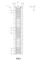
- FIG. 1 is a plan view showing an optical waveguide manufactured by an optical waveguide manufacturing method according to an embodiment.
- FIG. 2 is a cross-sectional view taken along line AA of FIG.
- FIG. 3 is a process diagram for explaining the method for manufacturing an optical waveguide according to the embodiment.
- FIG. 4 is a diagram for explaining the method of manufacturing the optical waveguide shown in FIG. 3, and is an enlarged view of a portion corresponding to a part of the optical waveguide shown in FIG.
- FIG. 5 is a diagram for explaining the method of manufacturing the optical waveguide shown in FIG. 3, and is an enlarged view of a portion corresponding to a part of the optical waveguide shown in FIG.
- FIG. 6 is a diagram for explaining the method of manufacturing the optical waveguide shown in FIG.
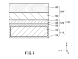
- FIG. 7 is a partially enlarged view of the metal plate and the intermediate film shown in FIG. 4(a).
- FIG. 8 is a table showing the results of various evaluation tests on the three-layer film as an example of the intermediate film shown in FIG. 7 and the silicone rubber sheet as a comparative film.
- FIG. 1 is a plan view showing an optical waveguide manufactured by an optical waveguide manufacturing method according to an embodiment.
- FIG. 2 is a cross-sectional view taken along line AA of FIG.
- the X-axis, Y-axis and Z-axis are set as three mutually orthogonal axes and indicated by arrows.
- the tip side of the arrow is called the “plus side” and the base side is called the “minus side”.
- the tip side of the arrow representing the Z axis is called “upper”, and the base end side is called “lower”. It should be noted that “upper” and “lower” in the following description do not limit the orientation with respect to the vertical direction during manufacture or use of the optical waveguide.
- the optical waveguide 1 shown in FIGS. 1 and 2 has a sheet shape, and includes a lower cover layer 18, a lower clad layer 11, a core layer 13, an upper clad layer 12 and an upper cover layer 19 in this order. It comprises a laminate structure that is laminated. Each layer of the optical waveguide 1 extends along the XY plane.
- the optical waveguide 1 is, for example, a long resin film having a long axis along the X axis, and has flexibility. Therefore, the optical waveguide 1 can be used even when it is bent along the circumference around the Y-axis, for example.
- the core layer 13 includes, as shown in FIG. 1, nine elongated core portions 14 extending along the X-axis and side clad portions 15 adjacent to the side surfaces of each core portion 14 . Therefore, the side clad portions 15 are adjacent to both side surfaces of the core portion 14 in the Y-axis direction. Further, as shown in FIG. 2 , the lower clad layer 11 is adjacent to the lower surface of the core portion 14 , and the upper clad layer 12 is adjacent to the upper surface of the core portion 14 . As a result, a sufficiently large refractive index difference is stably maintained between the core portion 14 and the clad portions (the side clad portion 15, the lower clad layer 11 and the upper clad layer 12). more efficient.
- the core portion 14 may be branched in the middle of the core layer 13 or may intersect with another core portion 14 in the middle.
- the number of core portions 14 provided in the core layer 13 is not particularly limited, and is, for example, about 1 to 100.
- the total length of the optical waveguide 1 along the X-axis is not particularly limited, but is preferably about 10 to 3000 mm.
- the total width of the optical waveguide 1 along the Y-axis is not particularly limited, but it is more preferably about 2 to 200 mm.
- the film thickness of the core layer 13 along the Z-axis is not particularly limited, it is preferably about 1 to 200 ⁇ m, more preferably about 5 to 100 ⁇ m, even more preferably about 10 to 70 ⁇ m. This ensures the optical properties and mechanical strength required for the core layer 13 .
- the thicknesses of the lower clad layer 11 and the upper clad layer 12 along the Z-axis are preferably about 1 to 200 ⁇ m, more preferably about 3 to 100 ⁇ m, and more preferably about 5 to 50 ⁇ m. More preferred. Thereby, the optical properties and mechanical strength required for the lower clad layer 11 and the upper clad layer 12 are ensured.
- the amount of cure shrinkage of the clad-forming layer is suppressed from becoming too large, and the influence thereof is suppressed from reaching the core layer 13. can be done.
- the optical waveguide 1 has an end face 101 located at the end on the negative side of the X axis and an end face 102 located at the end on the positive side of the X axis.
- the end surfaces 101 and 102 each function as a light entrance/exit surface.
- An optical connector (not shown) may be attached to at least one of both ends of the optical waveguide 1 .
- the optical waveguide 1 and other optical components can be fixed, and the end faces 101, 102 and other optical components can be optically connected.
- the optical waveguide 1 may have a mirror that changes the optical path of light passing through the core portion 14 . By converting the optical path through the mirror, the core portion 14 and optical components provided outside the optical waveguide 1 can be optically connected.
- the lower cover layer 18 is laminated on the lower surface of the lower clad layer 11 .
- the upper cover layer 19 is laminated on the upper surface of the upper clad layer 12 . Thereby, the mechanical properties and durability of the optical waveguide 1 can be enhanced. At least one of the lower cover layer 18 and the upper cover layer 19 may be omitted.
- the thickness of the optical waveguide 1 along the Z-axis is preferably 50-300 ⁇ m, more preferably 60-200 ⁇ m, even more preferably 70-150 ⁇ m. Thereby, the mechanical strength of the optical waveguide 1 can be sufficiently ensured while increasing the flexibility of the optical waveguide 1 .
- FIG. 3 is a process diagram for explaining the method for manufacturing an optical waveguide according to the embodiment.
- 4 to 6 are views for explaining the method of manufacturing the optical waveguide shown in FIG. 3, and are enlarged views of a portion corresponding to a part of the optical waveguide shown in FIG.
- the method for manufacturing the optical waveguide 1 shown in FIG. It has a stacking step S114 and a lower clad forming step S116.
- the pre-exposure laminate 180 including the core film 200, the intermediate film 120 and the metal plate 110, and the clad films 401 and 402 including the clad forming layer 170 are prepared.
- the exposure step S ⁇ b>104 a portion of the core forming layer 160 is irradiated with actinic radiation R to obtain an exposed laminate 190 .
- the post-exposure laminate 190 is heated to obtain the core layer 13 including the core portion 14 and the side clad portions 15 from the core forming layer 160 .
- the upper clad lamination step S108 the upper surface of the core layer 13 and the clad formation layer 170 are laminated.
- the laminated body of the core layer 13 and the clad forming layer 170 is heated to obtain the upper clad layer 12 from the clad forming layer 170.
- FIG. in the peeling step S ⁇ b>112 the base material 100 is peeled off from the lower surface of the core layer 13 .
- the lower clad laminating step S114 the lower surface of the core layer 13 and the clad formation layer 170 are laminated.
- the laminate of the core layer 13 and the clad forming layer 170 is heated to obtain the lower clad layer 11 from the clad forming layer 170.
- FIG. Each step will be described below in order.
- a pre-exposure laminate 180 including a core film 200, an intermediate film 120 and a metal plate 110 is prepared.
- the negative direction of the Z-axis is defined as the "laminating direction”
- the core film 200, the intermediate film 120 and the metal plate 110 are laminated in this order in the laminating direction.
- a clad film 402 having an upper cover layer 19 and a clad forming layer 170 laminated on the lower surface of the upper cover layer 19 is prepared.
- a clad film 401 having a lower cover layer 18 and a clad forming layer 170 laminated on the upper surface of the lower cover layer 18 is prepared.
- a core film 200 shown in FIG. 4A is a laminate of a substrate 100 and a core forming layer 160 .
- the core film 200 is in the form of a film, and may be in the form of a sheet or a roll that can be wound up.
- Examples of the method for forming the core forming layer 160 include a method of applying a varnish-like core-forming resin composition onto the substrate 100 and then drying, and a method of laminating a resin film on the substrate 100. .
- the method of applying the resin composition for example, a method of applying using various coaters such as a spin coater, a die coater, a comma coater and a curtain coater, a printing method such as screen printing, and the like are used.
- various coaters such as a spin coater, a die coater, a comma coater and a curtain coater, a printing method such as screen printing, and the like are used.
- a film-like resin film prepared from a varnish-like core-forming resin composition is subjected to, for example, roll lamination, vacuum roll lamination, flat plate lamination, vacuum flat plate lamination, normal pressure press, vacuum press, and the like.
- roll lamination vacuum roll lamination
- flat plate lamination flat plate lamination
- vacuum flat plate lamination normal pressure press
- vacuum press vacuum press
- the core film 200 may include a plurality of regions corresponding to the optical waveguides 1 so that a plurality of optical waveguides 1 can be finally cut out. In this case, by adding a step of cutting out the optical waveguide 1, the optical waveguide 1 can be manufactured more efficiently.
- Substrate A resin film is used for the substrate 100, for example.
- the constituent material of the base material 100 include polyolefins such as polyethylene terephthalate (PET), polyethylene naphthalate (PEN), polyethylene and polypropylene, polyimide, polyamide, polyetherimide, polyamideimide, and polytetrafluoroethylene (PTFE). fluororesins, polycarbonates, polyether sulfones, polyphenylene sulfides, liquid crystal polymers, and the like.
- the base material 100 may be subjected, if necessary, to release treatment or the like for facilitating separation between the core layer 13 and the base material 100 .
- Core-Forming Resin Composition examples include compositions containing a polymer, a monomer, a polymerization initiator, and the like.
- polymers include acrylic resins, methacrylic resins, polycarbonate, polystyrene, cyclic ether resins such as epoxy resins and oxetane resins, polyamides, polyimides, polybenzoxazoles, polysilanes, polysilazanes, silicone resins, Fluorine resin, polyurethane, polyolefin resin, polybutadiene, polyisoprene, polychloroprene, polyester such as PET and PBT, polyethylene succinate, polysulfone, polyether, and cyclic olefin such as benzocyclobutene resin and norbornene resin and phenoxy resins, etc., and one or more of these may be used in combination as polymer alloys, polymer blends (mixtures), copolymers, and the like.
- acrylic resins phenoxy resins, or cyclic olefin resins are preferably used as polymers.
- acrylic resins include monofunctional acrylates, polyfunctional acrylates, monofunctional methacrylates, polyfunctional methacrylates, urethane acrylates, urethane methacrylates, epoxy acrylates, epoxy methacrylates, polyester acrylates, and urea acrylates.
- examples include polymers of acrylic compounds containing one or more.
- the acrylic resin may have a polyester skeleton, a polypropylene glycol skeleton, a bisphenol skeleton, a fluorene skeleton, a tricyclodecane skeleton, a dicyclopentadiene skeleton, or the like.
- phenoxy resins include compounds containing bisphenol A, bisphenol A type epoxy compounds or their derivatives, and bisphenol F, bisphenol F type epoxy compounds or their derivatives as structural units of copolymer components.
- the content of the polymer is, for example, preferably 15% by mass or more, more preferably 40% by mass or more, and even more preferably 60% by mass or more of the total solid content of the core-forming resin composition. . This improves the mechanical properties of the core layer 13 .
- the polymer content in the core-forming resin composition is preferably 95% by mass or less, more preferably 90% by mass or less, of the total solid content of the core-forming resin composition. This improves the optical properties of the core layer 13 .
- the total solid content of the core-forming resin composition refers to the non-volatile content in the composition, and refers to the remainder after excluding volatile components such as water and solvents.
- the monomer is not particularly limited as long as it is a compound having a polymerizable site in its molecular structure. Examples include acrylic acid (methacrylic acid) monomers, epoxy monomers, oxetane monomers, norbornene monomers, vinyl ether system monomers, styrene-based monomers, photodimerization monomers, etc., and one or more of these may be used in combination.
- acrylic acid (methacrylic acid)-based monomers or epoxy-based monomers are preferably used as monomers.
- acrylic acid (methacrylic acid)-based monomers include compounds having two or more ethylenically unsaturated groups, bifunctional or trifunctional (meth)acrylates, and the like. Specifically, for example, aliphatic (meth)acrylates, alicyclic (meth)acrylates, aromatic (meth)acrylates, heterocyclic (meth)acrylates, or ethoxylated, propoxylated, ethoxylated propoxylated products, caprolactone modified products, and the like.
- the molecule may have a bisphenol skeleton, a urethane skeleton, or the like.
- Epoxy-based monomers include, for example, alicyclic epoxy compounds, aromatic epoxy compounds, and aliphatic epoxy compounds.
- a photopolymerizable monomer that reacts to form a reactant in the irradiated region upon irradiation with actinic radiation R such as visible light, ultraviolet light, infrared light, laser light, electron beam, and X-rays may be used.
- actinic radiation R such as visible light, ultraviolet light, infrared light, laser light, electron beam, and X-rays
- the monomer can move in the in-plane direction perpendicular to the film thickness in the core forming layer 160 when irradiated with the activating radiation R, and in the core layer 13 obtained as a result, the region irradiated with the activating radiation R and the A refractive index difference may be generated between the non-irradiated areas.
- the core portion 14 and the side clad portions 15 in the core layer 13 are formed based on the refractive index difference of the constituent materials. For example, a refractive index distribution can be formed in the core layer 13 by using different materials for the core portion 14 and the side clad portion 15 .
- a constituent material of the core layer 13 there is a leaving group (leaving pendant group) that is branched from the main chain and at least a part of the molecular structure of which can be released from the main chain by irradiation with actinic radiation.
- a method using a polymer can be used.
- the polymer can form a refractive index difference depending on whether or not it is irradiated with actinic radiation, thereby forming a refractive index distribution in the core layer 13.
- the core layer 13 contains a polymer and a monomer, and the concentration difference of the monomer or the concentration difference of the structure derived from the monomer is has a refractive index distribution based on
- the content of the monomer is preferably 1 part by mass or more and 70 parts by mass or less, more preferably 10 parts by mass or more and 60 parts by mass or less, relative to 100 parts by mass of the polymer.
- the polymerization initiator is appropriately selected according to the type of monomer polymerization reaction or crosslinking reaction.
- examples of polymerization initiators that can be used include radical polymerization initiators such as acrylic acid (methacrylic acid)-based monomers and styrene-based monomers, and cationic polymerization initiators such as epoxy-based monomers, oxetane-based monomers, and vinyl ether-based monomers.
- radical polymerization initiators examples include benzophenones and acetophenones. Specific examples include Irgacure (registered trademark) 651, Irgacure 819, Irgacure 2959, and Irgacure 184 (manufactured by IGM Japan LLC).
- cationic polymerization initiators include Lewis acid-generating compounds such as diazonium salts, and Bronsted acid-generating compounds such as iodonium salts and sulfonium salts.
- Lewis acid-generating compounds such as diazonium salts
- Bronsted acid-generating compounds such as iodonium salts and sulfonium salts.
- ADEKA OPTOMER SP-170 manufactured by ADEKA Co., Ltd.
- SAN-AID SI-100L manufactured by Sanshin Chemical Industry Co., Ltd.
- Rhodorsil 2074 manufactured by Rhodia Japan Co., Ltd.
- the content of the polymerization initiator is preferably 0.01 parts by mass or more and 5 parts by mass or less, more preferably 0.05 parts by mass or more and 3 parts by mass or less, relative to 100 parts by mass of the polymer.
- the core-forming resin composition includes, for example, a cross-linking agent, a sensitizer (photosensitizer), a catalyst precursor, a co-catalyst, an antioxidant, an ultraviolet absorber, a light stabilizer, a silane coupling agent, and a coating surface. It further contains modifiers, thermal polymerization inhibitors, leveling agents, surfactants, colorants, storage stabilizers, plasticizers, lubricants, fillers, inorganic particles, deterioration inhibitors, wettability improvers, antistatic agents, etc. good too.
- the above components are added to a solvent and stirred to obtain a varnish-like core-forming resin composition.
- the composition obtained may be subjected to a filtration treatment, for example through a PTFE filter with a pore size of 0.2 ⁇ m.
- the obtained composition may be subjected to a mixing treatment using various mixers.
- Solvents contained in the core-forming resin composition include, for example, acetone, methyl ethyl ketone, methyl isobutyl ketone, toluene, ethyl acetate, cyclohexane, methylcyclohexane, heptane, cyclohexanone, tetrahydrofuran, dimethylformamide, dimethylacetamide, dimethylsulfoxide, and ethylene glycol.
- ethylene glycol monomethyl ether ethylene glycol monoethyl ether, propylene glycol monomethyl ether, propylene glycol monoethyl ether, diethylene glycol dimethyl ether, ethylene glycol monomethyl ether acetate, propylene glycol monomethyl ether acetate, cellosolve series, carbitol series, anisole, N-methyl
- organic solvents such as pyrrolidone, and one or a mixture of two or more of these is used.
- the metal plate 110 shown in FIG. 4A is a support plate that supports the core film 200 with the intermediate film 120 interposed therebetween. By using such a metal plate 110, the handleability of the pre-exposure laminate 180 can be improved. This facilitates the operation of transporting the pre-exposure laminate 180 by the transport device.
- the metal plate 110 has superior rigidity and thermal conductivity compared to resin plates, glass plates, and the like. Therefore, by supporting the core film 200 with the metal plate 110, the flatness of the pre-exposure laminate 180 can be improved, and the in-plane temperature uniformity can be improved in a short time. By improving the flatness, when irradiating the pre-exposure laminate 180 with the actinic radiation R in a step described later, it is easy to improve the positional accuracy of the irradiated region. Thereby, the core portion 14 having excellent dimensional accuracy can be formed. In addition, by increasing the in-plane temperature uniformity in a short time, when the post-exposure laminate 190 is heated in the process described later, the temperature unevenness in the core forming layer 160 is suppressed. Variation in refractive index difference with the side clad portion 15 is suppressed. As a result, it is possible to manufacture the optical waveguide 1 with little variation in transmission loss between the core portions 14 .
- the metal material included in the metal plate 110 examples include all metal materials, such as aluminum, iron, copper, silver, titanium, magnesium, zinc, tin, nickel, etc., or alloys or intermetallic compounds containing these. etc.
- the metal material is preferably aluminum or an aluminum alloy. They are lightweight and have excellent chemical resistance and thermal conductivity. Therefore, the metal plate 110 containing these aluminum-based materials contributes to the formation of a high-quality core layer 13 that is highly transportable and highly durable, and has a particularly small variation in refractive index difference.
- metal plate 110 may contain materials other than metal materials, such as ceramic materials, glass materials, resin materials, silicon materials, and carbon materials.
- the thermal conductivity of the metal material included in the metal plate 110 is preferably 50 [W/(m ⁇ K)] or more, more preferably 100 [W/(m ⁇ K)] or more. If the thermal conductivity of the metal material is within the above range, the thermal conductivity of the metal plate 110 can be particularly enhanced. As a result, the temperature of the core forming layer 160 can be raised in a short period of time when the post-exposure laminate 190 is heated in the process described later. As a result, it is possible to reduce the time required for the heat treatment of the post-exposure laminate 190 while suppressing temperature unevenness in the core forming layer 160 .
- the thermal conductivity of the metal plate 110 is also set within the above range. Accordingly, even when the metal plate 110 contains a material other than a metal material, the above effects can be obtained.
- FIG. 7 is a partially enlarged view of the metal plate 110 shown in FIG. 4(a).
- the metal plate 110 may be a single plate containing a metal material in its entirety, but as shown in FIG. may be Coating 114 may cover the entire base portion 112 , but may be provided at least on the substrate 100 side.
- the coating 114 is a low-reflection portion having a lower reflectance for actinic radiation R than the base portion 112 .
- the reflectance of actinic radiation R of metal plate 110 can be reduced compared to the case where coating 114 is not provided.
- the metal plate 110 becomes the base of the core film 200 via the intermediate film 120 . Therefore, if the reflectance of the active radiation R is low, the active radiation R transmitted through the core film 200 is reflected by the metal plate 110 and returns to the core film 200 again via the intermediate film 120. occurrence is suppressed.
- the returned light causes the boundary between the active radiation R irradiation region 301 and the non-irradiation region 302 to fluctuate in the core forming layer 160 .
- the gradient of the refractive index between the core portion 14 formed from the core forming layer 160 and the side clad portion 15 becomes gentle, which may cause an increase in transmission loss. Therefore, by using the metal plate 110 as shown in FIG. 7, a high-quality core layer 13 can be formed.
- Examples of the coating 114 include a coating film, a wrapping film, a plating film, a vapor deposition film, and the like.
- the coating 114 may contain, in addition to the base component, additives such as black or dark-colored pigments and actinic radiation R absorbers such as ultraviolet absorbers.
- the reflectance of the actinic radiation R in the coating 114 should be lower than the reflectance of the actinic radiation R in the base portion 112 .
- the actinic radiation R for example, ultraviolet rays having a wavelength of 300 to 400 nm are used.
- the reflectance of ultraviolet light with a wavelength of 365 nm in the coating 114 is preferably 20% or less, more preferably 10% or less. Thereby, the reflectance of the actinic radiation R in the coating 114 can be further reduced.
- the UV reflectance of the coating 114 is a ratio calculated by dividing the intensity of the reflected UV measured at a distance of 7 cm from the coating 114 by the intensity of the irradiated UV directly received from the radiation source.
- the thickness of the metal plate 110 is not particularly limited, it is preferably 10 mm or less, more preferably 0.3 mm or more and 5 mm or less. As a result, the rigidity and in-plane thermal conductivity can be sufficiently secured while avoiding the metal plate 110 from becoming too heavy, and the flatness and in-plane temperature uniformity of the pre-exposure laminate 180 can be further enhanced. be able to.
- the intermediate film 120 shown in FIG. 4A is a film provided between the core film 200 and the metal plate 110 to fix them together. By using such an intermediate film 120, fixing and releasing of the core film 200 to the metal plate 110 can be easily performed.
- FIG. 7 also shows a partially enlarged view of the intermediate film 120 shown in FIG. 4(a).
- the intermediate film 120 may be a single layer member such as a silicone rubber sheet, but as shown in FIG. It may be.
- the radiation absorbing layer 124 is provided between the base material 100 and the metal plate 110 and has a function of absorbing the actinic radiation R.
- the intermediate film 120 included in the pre-exposure laminate 180 shown in FIG. 4(a) is a multi-layered structure including a radiation absorbing layer 124 having such a function.
- the radiation absorbing layer 124 absorbs the actinic radiation R transmitted through the core film 200 and reduces the amount of reflection. Therefore, the radiation absorbing layer 124 can contribute to suppression of returned light and suppress unintended photoreaction in the core forming layer 160 .
- the radiation absorbing layer 124 examples include polyimide film, polyester film, polyvinyl chloride film, polyethylene film, and polypropylene film. It is also possible to use a film in which an additive such as an ultraviolet absorber or carbon black is added to the base resin to increase the absorbance of the actinic radiation R of the resin.
- the radiation absorbing layer 124 is preferably a polyimide film.
- Polyimide films exhibit good absorption in the wavelength range, such as ultraviolet light, without the addition of additives. Therefore, by using a polyimide film, it is possible to obtain the radiation absorbing layer 124 exhibiting a function of absorbing the actinic radiation R stably and evenly.
- the polyimide film is excellent in heat resistance. Therefore, even if the pre-exposure laminate 180 having a polyimide film is subjected to heat treatment, deterioration is suppressed.
- the film thickness of the radiation absorbing layer 124 is not particularly limited, it is preferably 30 to 150 ⁇ m, more preferably 50 to 100 ⁇ m. This makes it possible to sufficiently secure the amount of actinic radiation R absorbed by the radiation absorbing layer 124 while suppressing variations in the amount of absorption due to excessive thickness.
- the intermediate film 120 included in the pre-exposure laminate 180 further includes a first adhesive layer 122 and a second adhesive layer as shown in FIG. 126 is provided.
- the first adhesive layer 122 is provided between the radiation absorbing layer 124 and the substrate 100 and has adhesiveness.
- the second adhesive layer 126 is provided between the radiation absorbing layer 124 and the metal plate 110 and has stronger adhesiveness than the first adhesive layer 122 .
- the metal plate 110 and the base material 100 can be easily laminated or unlaminated via the radiation absorbing layer 124. .
- the difference in adhesiveness as described above it is possible to suppress peeling of the intermediate film 120 from the metal plate 110 when the core film 200 is peeled off from the intermediate film 120 . Thereby, the work of peeling the core film 200 from the intermediate film 120 can be performed efficiently.
- the intermediate film 120 can be stably attached to the metal plate 110 , the intermediate film 120 can be reused together with the metal plate 110 . In other words, the intermediate film 120 that has been used once can be used together with the metal plate 110 to manufacture a new optical waveguide 1 .
- first adhesive layer 122 and the second adhesive layer 126 may have the same adhesiveness.
- Examples of the constituent materials of the first adhesive layer 122 and the second adhesive layer 126 include silicone-based adhesives, acrylic-based adhesives, and urethane-based adhesives, with silicone-based adhesives being particularly preferred. Since the silicone-based pressure-sensitive adhesive has excellent heat resistance, it is less likely that problems associated with heat treatment will occur.
- the thickness of the intermediate film 120 is not particularly limited, it is preferably 50-400 ⁇ m, more preferably 100-300 ⁇ m. Thereby, the handleability of the intermediate film 120 is improved.
- the intermediate film 120 may be subjected to dehumidification treatment before use. Thereby, the moisture adsorbed on the intermediate film 120 can be removed. As a result, it is possible to suppress problems associated with desorption of adsorbed moisture due to heat treatment.
- FIG. 8 is a table showing the results of various evaluation tests performed on the following three-layer film, which is an example of the intermediate film 120 shown in FIG. 7, and the following silicone rubber sheet as a comparative film.
- the three-layer film is a multilayer film with a three-layer structure consisting of a 75 ⁇ m thick silicone adhesive layer, a 75 ⁇ m thick polyimide film, and a 75 ⁇ m thick silicone adhesive layer.
- the silicone rubber sheet is a silicone rubber sheet with a thickness of 225 ⁇ m.
- the evaluation test is the measurement of the i-line transmittance and the measurement of the transmission loss of the optical waveguide test piece manufactured using the three-layer film (intermediate film 120) and the silicone rubber sheet (comparative film).
- the i-line is ultraviolet light with a wavelength of 365 nm.
- the width of the core portion 14 was set to 40 ⁇ m
- the width of the side clad portion 15 was set to 62.5 ⁇ m
- the line shape of the core portion 14 was set to be a straight line. Two types of curved test pieces with a radius of 10 mm are produced.
- the core film 200, the intermediate film 120 or the comparative film, and the test piece made of the stainless steel plate are irradiated with i-rays as active radiation R from the core film 200 side.
- the optical waveguide test piece comprises a core layer 13 including side clad portions 15 corresponding to the irradiated regions and core portions 14 corresponding to the non-irradiated regions.
- the stainless steel plate is intentionally configured to reflect the i-line. Therefore, the evaluation test shown in FIG. 8 is a test that can evaluate the significance of using the intermediate film 120 .
- the i-line transmittance was obtained by irradiating an i-line from the side of the base material 100 and measuring the intensity of the i-line transmitted to the glass substrate side for an evaluation body consisting of the base material 100, the intermediate film 120 or the comparative film, and the glass substrate. is the transmittance calculated by
- the transmission loss is measured according to the insertion loss measurement method stipulated in the JPCA (Japan Electronic Circuits Association) standard "Polymer Optical Waveguide Test Method (JPCA-PE02-05-01S-2008)". It is a measured value.
- the length of the optical waveguide test piece is 7 cm.
- the i-line transmittance of the evaluation sample including the three-layer film (intermediate film 120) is 0%.
- the i-ray transmittance of the evaluation sample containing the silicone rubber sheet (comparative film) was 98%. From this evaluation result, the three-layer film as the intermediate film 120 exhibits high absorbability for the actinic radiation R to such an extent that the i-line is almost blocked.
- the optical waveguide test piece manufactured with the three-layer film (intermediate film 120) as the base has a higher transmission loss than the optical waveguide test piece manufactured with the silicone rubber sheet (comparative film) as the base. is kept small. Therefore, FIG. 8 confirms that an optical waveguide with low transmission loss can be manufactured by using the intermediate film 120 including a radiation absorbing layer that absorbs actinic radiation R.
- FIG. 8 confirms that an optical waveguide with low transmission loss can be manufactured by using the intermediate film 120 including a radiation absorbing layer that absorbs actinic radiation R.
- the clad film 401 is a laminate of the lower cover layer 18 and the clad forming layer 170 .
- the clad film 402 is a laminate of the upper cover layer 19 and the clad forming layer 170 .
- These clad films 401 and 402 are film-shaped, and may be sheet-shaped or roll-shaped.
- Examples of the method of forming the clad forming layer 170 include a method of applying a varnish-like clad forming resin composition onto the cover layer and then drying, and a method of laminating a resin film on the cover layer.
- the method of applying the resin composition for example, a method of applying using various coaters such as a spin coater, a die coater, a comma coater and a curtain coater, a printing method such as screen printing, and the like are used.
- various coaters such as a spin coater, a die coater, a comma coater and a curtain coater, a printing method such as screen printing, and the like are used.
- a film-like resin film prepared from a varnish-like clad-forming resin composition is subjected to, for example, roll lamination, vacuum roll lamination, flat plate lamination, vacuum flat plate lamination, normal pressure press, vacuum press, and the like.
- roll lamination vacuum roll lamination
- flat plate lamination flat plate lamination
- vacuum flat plate lamination normal pressure press
- vacuum press vacuum press
- the film thickness of the lower cover layer 18 and the upper cover layer 19 is not particularly limited, but is preferably about 1 to 200 ⁇ m, more preferably about 3 to 100 ⁇ m, and more preferably about 5 to 50 ⁇ m. is more preferred. If the film thickness of each cover layer is within the above range, the ability to protect the core layer 13 and the like by the lower cover layer 18 and the upper cover layer 19 can be ensured, while the adverse effects of the optical waveguide 1 becoming too thick, such as A decrease in the flexibility of the optical waveguide 1 can be suppressed.
- the film thicknesses of the lower cover layer 18 and the upper cover layer 19 may be different from each other, but are preferably the same. As a result, warping of the optical waveguide 1 due to the difference in film thickness can be suppressed. Note that the same film thickness means that the difference in film thickness is 5 ⁇ m or less.
- Main materials of the lower cover layer 18 and the upper cover layer 19 include, for example, polyolefins such as polyethylene terephthalate (PET), polyethylene naphthalate (PEN), polyethylene, polypropylene, polyimide, polyamide, polyetherimide, polyamideimide, Materials containing various resins such as fluorine resin such as polytetrafluoroethylene (PTFE), polycarbonate, polyether sulfone, polyphenylene sulfide, and liquid crystal polymer can be used.
- polyolefins such as polyethylene terephthalate (PET), polyethylene naphthalate (PEN), polyethylene, polypropylene, polyimide, polyamide, polyetherimide, polyamideimide, Materials containing various resins such as fluorine resin such as polytetrafluoroethylene (PTFE), polycarbonate, polyether sulfone, polyphenylene sulfide, and liquid crystal polymer can be used.
- PTFE polytetrafluor
- the main materials of the lower cover layer 18 and the upper cover layer 19 may be different from each other, but are preferably the same as each other. As a result, warping of the optical waveguide 1 due to the difference in the main material can be suppressed.
- the modulus of elasticity of the lower cover layer 18 and the upper cover layer 19 is preferably 1 to 12 GPa, more preferably 2 to 11 GPa, even more preferably 3 to 10 GPa.
- the above elastic modulus is a tensile elastic modulus measured according to the method specified in JIS K 7161-1:2014.
- Clad-Forming Resin Composition examples include compositions containing a polymer, a monomer, a polymerization initiator, and the like.
- polymers include acrylic resins, methacrylic resins, polycarbonate, polystyrene, cyclic ether resins such as epoxy resins and oxetane resins, polyamides, polyimides, polybenzoxazoles, polysilanes, polysilazanes, silicone resins, Fluorine resin, polyurethane, polyolefin resin, polybutadiene, polyisoprene, polychloroprene, polyester such as PET and PBT, polyethylene succinate, polysulfone, polyether, and cyclic olefin such as benzocyclobutene resin and norbornene resin and phenoxy resins, etc., and one or more of these may be used in combination as polymer alloys, polymer blends (mixtures), copolymers, and the like.
- acrylic resins phenoxy resins, or cyclic olefin resins are preferably used as polymers.
- acrylic resins include monofunctional acrylates, polyfunctional acrylates, monofunctional methacrylates, polyfunctional methacrylates, urethane acrylates, urethane methacrylates, epoxy acrylates, epoxy methacrylates, polyester acrylates, and urea acrylates.
- examples include polymers of acrylic compounds containing one or more.
- the acrylic resin may have a polyester skeleton, a polypropylene glycol skeleton, a bisphenol skeleton, a fluorene skeleton, a tricyclodecane skeleton, a dicyclopentadiene skeleton, or the like.
- phenoxy resins include compounds containing bisphenol A, bisphenol A type epoxy compounds or their derivatives, and bisphenol F, bisphenol F type epoxy compounds or their derivatives as structural units of copolymer components.
- the polymer may contain a thermosetting resin as needed.
- thermosetting resins include amino resins, isocyanate compounds, blocked isocyanate compounds, maleimide compounds, benzoxazine compounds, oxazoline compounds, carbodiimide compounds, cyclocarbonate compounds, polyfunctional oxetane compounds, episulfide resins, and epoxy resins.
- the polymer content is, for example, preferably 15% by mass or more, more preferably 40% by mass or more, and even more preferably 60% by mass or more of the total solid content of the clad-forming resin composition. . Thereby, the mechanical properties of the lower clad layer 11 and the upper clad layer 12 are improved.
- the polymer content in the clad-forming resin composition is preferably 95% by mass or less, more preferably 90% by mass or less, of the total solid content of the clad-forming resin composition. Thereby, the optical properties of the lower clad layer 11 and the upper clad layer 12 are improved.
- the total solid content of the cladding-forming resin composition refers to the nonvolatile content in the composition, and refers to the remainder after excluding volatile components such as water and solvents.
- the monomer is not particularly limited as long as it is a compound having a polymerizable site in its molecular structure. Examples include acrylic acid (methacrylic acid) monomers, epoxy monomers, oxetane monomers, norbornene monomers, vinyl ether system monomers, styrene-based monomers, photodimerization monomers, etc., and one or more of these may be used in combination.
- acrylic acid (methacrylic acid)-based monomers or epoxy-based monomers are preferably used as monomers.
- acrylic acid (methacrylic acid)-based monomers include compounds having two or more ethylenically unsaturated groups, bifunctional or trifunctional (meth)acrylates, and the like. Specifically, for example, aliphatic (meth)acrylates, alicyclic (meth)acrylates, aromatic (meth)acrylates, heterocyclic (meth)acrylates, or ethoxylated, propoxylated, ethoxylated propoxylated products, caprolactone modified products, and the like.
- the molecule may have a bisphenol skeleton, a urethane skeleton, or the like.
- Epoxy-based monomers include, for example, alicyclic epoxy compounds, aromatic epoxy compounds, and aliphatic epoxy compounds.
- the content of the monomer is preferably 1 part by mass or more and 70 parts by mass or less, more preferably 10 parts by mass or more and 60 parts by mass or less, relative to 100 parts by mass of the polymer.
- the polymerization initiator is appropriately selected according to the type of monomer polymerization reaction or crosslinking reaction.
- examples of polymerization initiators that can be used include radical polymerization initiators such as acrylic acid (methacrylic acid)-based monomers and styrene-based monomers, and cationic polymerization initiators such as epoxy-based monomers, oxetane-based monomers, and vinyl ether-based monomers.
- radical polymerization initiators examples include benzophenones and acetophenones. Specific examples include Irgacure 651, Irgacure 819, Irgacure 2959, and Irgacure 184 (manufactured by IGM Japan LLC).
- cationic polymerization initiators include Lewis acid-generating compounds such as diazonium salts, and Bronsted acid-generating compounds such as iodonium salts and sulfonium salts.
- Lewis acid-generating compounds such as diazonium salts
- Bronsted acid-generating compounds such as iodonium salts and sulfonium salts.
- ADEKA OPTOMER SP-170 manufactured by ADEKA Co., Ltd.
- SAN-AID SI-100L manufactured by Sanshin Chemical Industry Co., Ltd.
- Rhodorsil 2074 manufactured by Rhodia Japan Co., Ltd.
- the content of the polymerization initiator is preferably 0.01 parts by mass or more and 5 parts by mass or less, more preferably 0.05 parts by mass or more and 3 parts by mass or less, relative to 100 parts by mass of the polymer.
- Cladding resin compositions include, for example, cross-linking agents, sensitizers (photosensitizers), catalyst precursors, co-catalysts, antioxidants, ultraviolet absorbers, light stabilizers, silane coupling agents, and coating surfaces. It further contains modifiers, thermal polymerization inhibitors, leveling agents, surfactants, colorants, storage stabilizers, plasticizers, lubricants, fillers, inorganic particles, deterioration inhibitors, wettability improvers, antistatic agents, etc. good too.
- a varnish-like cladding-forming resin composition is obtained by adding the components described above to a solvent and stirring the mixture.
- the composition obtained may be subjected to a filtration treatment, for example through a PTFE filter with a pore size of 0.2 ⁇ m.
- the obtained composition may be subjected to a mixing treatment using various mixers.
- Solvents contained in the clad-forming resin composition include, for example, acetone, methyl ethyl ketone, methyl isobutyl ketone, toluene, ethyl acetate, cyclohexane, methylcyclohexane, heptane, cyclohexanone, tetrahydrofuran, dimethylformamide, dimethylacetamide, dimethylsulfoxide, and ethylene glycol.
- ethylene glycol monomethyl ether ethylene glycol monoethyl ether, propylene glycol monomethyl ether, propylene glycol monoethyl ether, diethylene glycol dimethyl ether, ethylene glycol monomethyl ether acetate, propylene glycol monomethyl ether acetate, cellosolve series, carbitol series, anisole, N-methyl
- organic solvents such as pyrrolidone, and one or a mixture of two or more of these is used.
- the clad-forming resin composition for forming the lower clad layer 11 and the clad-forming resin composition for forming the upper clad layer 12 may be the same or different. good.
- Exposure Step In the exposure step S ⁇ b>104 , a portion of the core forming layer 160 included in the pre-exposure laminate 180 is irradiated with actinic radiation R in the stacking direction of the pre-exposure laminate 180 . A refractive index difference is formed between the irradiated region 301 and the non-irradiated region 302 in the core forming layer 160 irradiated with the actinic radiation R. FIG. As a result, the post-exposure laminate 190 shown in FIG. 5(d) is obtained.
- part of the actinic radiation R is absorbed by the intermediate film 120 described above after passing through the core film 200 . Thereby, it is possible to suppress return light that is reflected by the metal plate 110 and reaches the core film 200 .
- a method using a photomask 303 shown in FIG. 4(b) is used.
- an irradiation region 301 and a non-irradiation region 302 can be set corresponding to the mask pattern of the photomask 303 .
- a method using the direct exposure machine 304 may be adopted.
- actinic radiation R is applied by a direct exposure machine 304 .
- various spatial light modulators such as a reflective spatial light modulator such as a digital micromirror device (DMD) and a transmissive spatial light modulator such as a liquid crystal display device (LCD).
- DMD digital micromirror device
- LCD liquid crystal display device
- An exposure machine that can select an irradiation area using an element can be mentioned.
- a direct writing exposure machine 304 it is possible to set the irradiation area 301 and the non-irradiation area 302 without using the photomask 303 .
- the size of the irradiated region 301 and the non-irradiated region 302 can be adjusted without changing the photomask 303, so that the manufacturing cost of the optical waveguide 1 can be reduced and the efficiency can be improved.
- FIG. 4(b) and 4(c) illustrate the polymer 131 and the monomer 132 included in the core forming layer 160.
- FIG. In the core-forming layer 160 before irradiation with actinic radiation R, the monomers 132 are distributed almost uniformly in the polymer 131 .
- the monomer 132 and the structure derived from the monomer 132 have a lower refractive index than the polymer 131 .
- the post-exposure laminate 190 is heated. This heating activates the polymerization initiator present in the irradiated region 301 and causes the reaction of the monomer 132 to proceed. This enlarges or fixes the concentration difference of the monomer 132 . As a result, the concentration of the monomer 132 in the irradiated area 301 further increases and the concentration of the monomer 132 in the non-irradiated area 302 further decreases. As a result, the refractive index of the irradiated region 301 is lowered under the influence of the monomer 132 and the refractive index of the non-irradiated region 302 is increased under the influence of the polymer 131 .
- Heating conditions for the core forming layer 160 include, for example, a heating temperature of 100 to 200° C. and a heating time of 10 to 180 minutes.
- Examples of the heating method for the post-exposure laminate 190 include a contact heating method (contact baking) and a non-contact heating method (proximity baking).
- the non-contact heating method is preferably used. According to the non-contact heating method, the temperature of the core film 200 can be raised by transferring radiant heat to the metal plate 110 . Therefore, in-plane uniformity of the temperature of the core film 200 can be easily improved as compared with the contact heating method.
- the post-exposure laminate 190 since the post-exposure laminate 190 includes the metal plate 110, it has excellent thermal conductivity in the in-plane direction. For this reason, in this embodiment, as shown in FIG. 5E, by applying heat H from the lower side of the metal plate 110 (the side of the metal plate 110 opposite to the substrate 100), the post-exposure laminate 190 is to heat. Thereby, the temperature of the core film 200 can be raised through heat transfer to the metal plate 110 . Therefore, the in-plane temperature uniformity of the core film 200 can be further improved.
- the refractive index may change due to volatilization of the monomer 132 or change in the molecular structure of the polymer 131 accompanying this heating.
- the method of forming the core layer 13 is not limited to the above method.
- a photolithography method, a replication method, or the like may be used.
- the photolithography method is a method of forming the core portion 14 and the side clad portion 15 with materials having different refractive indexes by combining exposure/development technology and etching technology.
- the duplication method is a method in which, for example, a mold having a core pattern is pressed against a resin film to form the core portion 14, and then the side clad portions 15 are formed.
- the core forming layer 160 before being irradiated with the activating radiation R or the core forming layer 160 after being irradiated with the activating radiation R may be surface-treated as necessary.
- surface treatment include plasma treatment, corona treatment, ultraviolet irradiation treatment, and electron beam irradiation treatment.
- a clad film 402 is laminated on the upper surface of the core layer 13, as shown in FIG. 5(f). As a result, a laminate of the core layer 13 and the clad film 402 is obtained as shown in FIG. 6(g). Specifically, the operation of stacking the clad film 402 is performed so that the clad forming layer 170 is in contact with the upper surface of the core layer 13 . This operation may be a single wafer operation or a roll-to-roll operation.
- Heating conditions include, for example, heating temperature: 100 to 200°C and heating time: 10 to 180 minutes.
- peeling Step S112 the substrate 100 is peeled from the first laminate. The remainder after peeling off the base material 100 is used as a second laminate 500 as shown in FIG. 6(h).
- the core layer 13 after peeling off the base material 100 may be subjected to surface treatment, if necessary.
- surface treatment include plasma treatment, corona treatment, ultraviolet irradiation treatment, and electron beam irradiation treatment.
- the clad film 401 is laminated on the lower surface of the core layer 13 of the second laminate 500.
- FIG. 6(i) a laminate of the core layer 13 and the clad film 401 is obtained as shown in FIG. 6(i).
- the operation of stacking the clad film 401 is performed so that the clad forming layer 170 is in contact with the lower surface of the core layer 13 .
- This operation may be a single wafer operation or a roll-to-roll operation.
- Heating conditions include, for example, a heating temperature of 100 to 200° C. and a heating time of 10 to 180 minutes. is preferred. As described above, the optical waveguide 1 shown in FIG. 2 is obtained.
- the optical waveguide manufacturing method includes the preparation step S102, the exposure step S104, and the core formation step S106.
- the preparation step S102 a pre-exposure laminate 180 in which the core forming layer 160, the base material 100 and the metal plate 110 are laminated in this order in the lamination direction is prepared.
- the exposure step S104 a portion of the core forming layer 160 in the plane thereof is irradiated with actinic radiation R in the stacking direction to obtain an exposed laminate 190 .
- the post-exposure laminate 190 is heated to obtain the core layer 13 including the core portion 14 and the side clad portions 15 from the core forming layer 160 .
- in-plane temperature uniformity can be ensured in a short time when the core forming layer 160 irradiated with the actinic radiation R is heated in the core forming step S106.
- variations in refractive index difference between the core portion 14 and the side clad portion 15 can be suppressed.
- the method for manufacturing an optical waveguide has an upper clad forming step S110, a peeling step S112, and a lower clad forming step S116.
- the upper clad forming step S110 the upper clad layer 12 (first clad layer) is formed so as to be in contact with the core layer 13 of the post-exposure laminate 190 to obtain the first laminate.
- the peeling step S ⁇ b>112 the base material 100 is peeled off from the first layered body, and the remainder is used as the second layered body 500 .
- the lower clad forming step S ⁇ b>116 the lower clad layer 11 (second clad layer) is formed so as to be in contact with the core layer 13 of the second laminate 500 .
- the optical waveguide 1 having a structure in which the core layer 13 is sandwiched between the lower clad layer 11 and the upper clad layer 12 is obtained.
- the optical waveguide 1 with small transmission loss can be efficiently manufactured.
- the method for manufacturing an optical waveguide of the present invention may add steps for any purpose to the above embodiments.
- in-plane temperature uniformity can be ensured in a short period of time when the core forming layer irradiated with actinic radiation is heated.
- a small number of optical waveguides can be efficiently manufactured. Therefore, the present invention has industrial applicability.
Landscapes
- Physics & Mathematics (AREA)
- Engineering & Computer Science (AREA)
- Microelectronics & Electronic Packaging (AREA)
- General Physics & Mathematics (AREA)
- Optics & Photonics (AREA)
- Optical Integrated Circuits (AREA)
Priority Applications (2)
| Application Number | Priority Date | Filing Date | Title |
|---|---|---|---|
| CN202280085131.7A CN118633047A (zh) | 2021-12-27 | 2022-10-25 | 光波导的制造方法 |
| JP2023507361A JP7311066B1 (ja) | 2021-12-27 | 2022-10-25 | 光導波路の製造方法 |
Applications Claiming Priority (2)
| Application Number | Priority Date | Filing Date | Title |
|---|---|---|---|
| JP2021-212865 | 2021-12-27 | ||
| JP2021212865 | 2021-12-27 |
Publications (1)
| Publication Number | Publication Date |
|---|---|
| WO2023127257A1 true WO2023127257A1 (ja) | 2023-07-06 |
Family
ID=86998640
Family Applications (1)
| Application Number | Title | Priority Date | Filing Date |
|---|---|---|---|
| PCT/JP2022/039791 Ceased WO2023127257A1 (ja) | 2021-12-27 | 2022-10-25 | 光導波路の製造方法 |
Country Status (4)
| Country | Link |
|---|---|
| JP (1) | JP7311066B1 (https=) |
| CN (1) | CN118633047A (https=) |
| TW (1) | TW202328719A (https=) |
| WO (1) | WO2023127257A1 (https=) |
Cited By (1)
| Publication number | Priority date | Publication date | Assignee | Title |
|---|---|---|---|---|
| WO2024204317A1 (ja) * | 2023-03-31 | 2024-10-03 | 住友ベークライト株式会社 | 樹脂組成物、フィルム、フィルムセット、光導波路、光電気複合基板、および電子部品 |
Citations (8)
| Publication number | Priority date | Publication date | Assignee | Title |
|---|---|---|---|---|
| JP2004341454A (ja) * | 2002-05-28 | 2004-12-02 | Matsushita Electric Works Ltd | 光電気混載基板の製造方法 |
| JP2006039231A (ja) * | 2004-07-27 | 2006-02-09 | Matsushita Electric Works Ltd | 光電気配線混載基板の製造方法 |
| JP2008012810A (ja) * | 2006-07-06 | 2008-01-24 | Kawamura Sangyo Kk | プラスチックフィルム−導体金属箔積層体の製造方法 |
| JP2009276724A (ja) * | 2008-05-19 | 2009-11-26 | Nitto Denko Corp | 光導波路装置の製造方法 |
| US20100172623A1 (en) * | 2008-12-10 | 2010-07-08 | Electronics And Telecommunications Research Institute | Compound containing crosslinkable moieties, prepolymer, blend and polymer sheet obtained therefrom, and waveguide for optical interconnection |
| JP2014199369A (ja) * | 2013-03-29 | 2014-10-23 | 住友ベークライト株式会社 | 光導波路および電子機器 |
| JP2015087660A (ja) * | 2013-10-31 | 2015-05-07 | 住友ベークライト株式会社 | 光導波路、光電気混載基板および電子機器 |
| JP2015087658A (ja) * | 2013-10-31 | 2015-05-07 | 住友ベークライト株式会社 | 光導波路、光電気混載基板および電子機器 |
-
2022
- 2022-10-25 JP JP2023507361A patent/JP7311066B1/ja active Active
- 2022-10-25 WO PCT/JP2022/039791 patent/WO2023127257A1/ja not_active Ceased
- 2022-10-25 CN CN202280085131.7A patent/CN118633047A/zh not_active Withdrawn
- 2022-10-31 TW TW111141338A patent/TW202328719A/zh unknown
Patent Citations (8)
| Publication number | Priority date | Publication date | Assignee | Title |
|---|---|---|---|---|
| JP2004341454A (ja) * | 2002-05-28 | 2004-12-02 | Matsushita Electric Works Ltd | 光電気混載基板の製造方法 |
| JP2006039231A (ja) * | 2004-07-27 | 2006-02-09 | Matsushita Electric Works Ltd | 光電気配線混載基板の製造方法 |
| JP2008012810A (ja) * | 2006-07-06 | 2008-01-24 | Kawamura Sangyo Kk | プラスチックフィルム−導体金属箔積層体の製造方法 |
| JP2009276724A (ja) * | 2008-05-19 | 2009-11-26 | Nitto Denko Corp | 光導波路装置の製造方法 |
| US20100172623A1 (en) * | 2008-12-10 | 2010-07-08 | Electronics And Telecommunications Research Institute | Compound containing crosslinkable moieties, prepolymer, blend and polymer sheet obtained therefrom, and waveguide for optical interconnection |
| JP2014199369A (ja) * | 2013-03-29 | 2014-10-23 | 住友ベークライト株式会社 | 光導波路および電子機器 |
| JP2015087660A (ja) * | 2013-10-31 | 2015-05-07 | 住友ベークライト株式会社 | 光導波路、光電気混載基板および電子機器 |
| JP2015087658A (ja) * | 2013-10-31 | 2015-05-07 | 住友ベークライト株式会社 | 光導波路、光電気混載基板および電子機器 |
Cited By (1)
| Publication number | Priority date | Publication date | Assignee | Title |
|---|---|---|---|---|
| WO2024204317A1 (ja) * | 2023-03-31 | 2024-10-03 | 住友ベークライト株式会社 | 樹脂組成物、フィルム、フィルムセット、光導波路、光電気複合基板、および電子部品 |
Also Published As
| Publication number | Publication date |
|---|---|
| CN118633047A (zh) | 2024-09-10 |
| TW202328719A (zh) | 2023-07-16 |
| JP7311066B1 (ja) | 2023-07-19 |
| JPWO2023127257A1 (https=) | 2023-07-06 |
Similar Documents
| Publication | Publication Date | Title |
|---|---|---|
| KR102747239B1 (ko) | 편광판 및 이 편광판을 구비하는 표시 장치, 그리고 그 제조 방법 | |
| KR102342126B1 (ko) | 광학 필름 및 광학 필름의 제조 방법 | |
| JP6662992B2 (ja) | 円偏光板の製造方法 | |
| JP7311066B1 (ja) | 光導波路の製造方法 | |
| WO2020026970A1 (ja) | 光導波路形成用感光性エポキシ樹脂組成物、光導波路形成用感光性フィルムおよびそれを用いた光導波路、光・電気伝送用混載フレキシブルプリント配線板 | |
| JP2016014846A (ja) | 近赤外線カットフィルタの製造方法および固体撮像素子 | |
| TWI452363B (zh) | 光波導的製造方法以及光波導 | |
| JP7414185B2 (ja) | 光導波路の製造方法 | |
| JP7367892B2 (ja) | 光導波路の製造方法 | |
| US20070190317A1 (en) | Anisotropic scattering adhesive member | |
| CN110073258B (zh) | 光波导形成用感光性环氧树脂组合物、光波导形成用固化性薄膜及使用其的光波导、光/电传输用混载挠性印刷电路板 | |
| JP7735786B2 (ja) | 光導波路の製造方法 | |
| TW201529702A (zh) | 光波導用感光性樹脂組成物及光波導芯層形成用光硬化性薄膜、以及使用其之光波導、光.電傳送用混合撓性印刷配線板 | |
| JP6274340B1 (ja) | 光導波路フィルムおよび光学部品 | |
| JP2023096847A (ja) | 光導波路の製造方法 | |
| CN110799865B (zh) | 光学膜 | |
| JP6183529B1 (ja) | 光導波路フィルムおよび光学部品 | |
| JP6183532B1 (ja) | 光導波路フィルムおよび光学部品 | |
| JP4929667B2 (ja) | 光学材料用樹脂組成物、光学材料用樹脂フィルム及びこれを用いた光導波路 | |
| TW202003248A (zh) | 光學積層體的製造方法 | |
| JP6888373B2 (ja) | 光導波路フィルムおよび光学部品 | |
| CN120051895A (zh) | 多层超表面结构体的制造方法及多层超表面结构体 | |
| JP2024100122A (ja) | 光導波路および光導波路の製造方法 | |
| TW202334719A (zh) | 偏光板及圖像顯示裝置 | |
| CN118176454A (zh) | 光学层叠体、光学装置、光学层叠体的制造方法 |
Legal Events
| Date | Code | Title | Description |
|---|---|---|---|
| WWE | Wipo information: entry into national phase |
Ref document number: 2023507361 Country of ref document: JP |
|
| 121 | Ep: the epo has been informed by wipo that ep was designated in this application |
Ref document number: 22915491 Country of ref document: EP Kind code of ref document: A1 |
|
| WWE | Wipo information: entry into national phase |
Ref document number: 18707893 Country of ref document: US |
|
| WWE | Wipo information: entry into national phase |
Ref document number: 202280085131.7 Country of ref document: CN |
|
| NENP | Non-entry into the national phase |
Ref country code: DE |
|
| 122 | Ep: pct application non-entry in european phase |
Ref document number: 22915491 Country of ref document: EP Kind code of ref document: A1 |