WO2023127187A1 - 窒化物半導体デバイス - Google Patents
窒化物半導体デバイス Download PDFInfo
- Publication number
- WO2023127187A1 WO2023127187A1 PCT/JP2022/028179 JP2022028179W WO2023127187A1 WO 2023127187 A1 WO2023127187 A1 WO 2023127187A1 JP 2022028179 W JP2022028179 W JP 2022028179W WO 2023127187 A1 WO2023127187 A1 WO 2023127187A1
- Authority
- WO
- WIPO (PCT)
- Prior art keywords
- nitride semiconductor
- semiconductor layer
- layer
- resistance
- semiconductor device
- Prior art date
- Legal status (The legal status is an assumption and is not a legal conclusion. Google has not performed a legal analysis and makes no representation as to the accuracy of the status listed.)
- Ceased
Links
Images


Classifications
-
- H—ELECTRICITY
- H10—SEMICONDUCTOR DEVICES; ELECTRIC SOLID-STATE DEVICES NOT OTHERWISE PROVIDED FOR
- H10D—INORGANIC ELECTRIC SEMICONDUCTOR DEVICES
- H10D30/00—Field-effect transistors [FET]
- H10D30/01—Manufacture or treatment
- H10D30/015—Manufacture or treatment of FETs having heterojunction interface channels or heterojunction gate electrodes, e.g. HEMT
-
- H—ELECTRICITY
- H10—SEMICONDUCTOR DEVICES; ELECTRIC SOLID-STATE DEVICES NOT OTHERWISE PROVIDED FOR
- H10D—INORGANIC ELECTRIC SEMICONDUCTOR DEVICES
- H10D30/00—Field-effect transistors [FET]
- H10D30/01—Manufacture or treatment
- H10D30/051—Manufacture or treatment of FETs having PN junction gates
-
- H—ELECTRICITY
- H10—SEMICONDUCTOR DEVICES; ELECTRIC SOLID-STATE DEVICES NOT OTHERWISE PROVIDED FOR
- H10D—INORGANIC ELECTRIC SEMICONDUCTOR DEVICES
- H10D30/00—Field-effect transistors [FET]
- H10D30/01—Manufacture or treatment
- H10D30/061—Manufacture or treatment of FETs having Schottky gates
-
- H—ELECTRICITY
- H10—SEMICONDUCTOR DEVICES; ELECTRIC SOLID-STATE DEVICES NOT OTHERWISE PROVIDED FOR
- H10D—INORGANIC ELECTRIC SEMICONDUCTOR DEVICES
- H10D30/00—Field-effect transistors [FET]
- H10D30/40—FETs having zero-dimensional [0D], one-dimensional [1D] or two-dimensional [2D] charge carrier gas channels
- H10D30/47—FETs having zero-dimensional [0D], one-dimensional [1D] or two-dimensional [2D] charge carrier gas channels having two-dimensional [2D] charge carrier gas channels, e.g. nanoribbon FETs or high electron mobility transistors [HEMT]
- H10D30/471—High electron mobility transistors [HEMT] or high hole mobility transistors [HHMT]
- H10D30/475—High electron mobility transistors [HEMT] or high hole mobility transistors [HHMT] having wider bandgap layer formed on top of lower bandgap active layer, e.g. undoped barrier HEMTs such as i-AlGaN/GaN HEMTs
-
- H—ELECTRICITY
- H10—SEMICONDUCTOR DEVICES; ELECTRIC SOLID-STATE DEVICES NOT OTHERWISE PROVIDED FOR
- H10D—INORGANIC ELECTRIC SEMICONDUCTOR DEVICES
- H10D30/00—Field-effect transistors [FET]
- H10D30/60—Insulated-gate field-effect transistors [IGFET]
-
- H—ELECTRICITY
- H10—SEMICONDUCTOR DEVICES; ELECTRIC SOLID-STATE DEVICES NOT OTHERWISE PROVIDED FOR
- H10D—INORGANIC ELECTRIC SEMICONDUCTOR DEVICES
- H10D30/00—Field-effect transistors [FET]
- H10D30/80—FETs having rectifying junction gate electrodes
- H10D30/83—FETs having PN junction gate electrodes
-
- H—ELECTRICITY
- H10—SEMICONDUCTOR DEVICES; ELECTRIC SOLID-STATE DEVICES NOT OTHERWISE PROVIDED FOR
- H10D—INORGANIC ELECTRIC SEMICONDUCTOR DEVICES
- H10D30/00—Field-effect transistors [FET]
- H10D30/80—FETs having rectifying junction gate electrodes
- H10D30/87—FETs having Schottky gate electrodes, e.g. metal-semiconductor FETs [MESFET]
-
- H—ELECTRICITY
- H10—SEMICONDUCTOR DEVICES; ELECTRIC SOLID-STATE DEVICES NOT OTHERWISE PROVIDED FOR
- H10D—INORGANIC ELECTRIC SEMICONDUCTOR DEVICES
- H10D62/00—Semiconductor bodies, or regions thereof, of devices having potential barriers
- H10D62/10—Shapes, relative sizes or dispositions of the regions of the semiconductor bodies; Shapes of the semiconductor bodies
- H10D62/102—Constructional design considerations for preventing surface leakage or controlling electric field concentration
-
- H—ELECTRICITY
- H10—SEMICONDUCTOR DEVICES; ELECTRIC SOLID-STATE DEVICES NOT OTHERWISE PROVIDED FOR
- H10D—INORGANIC ELECTRIC SEMICONDUCTOR DEVICES
- H10D62/00—Semiconductor bodies, or regions thereof, of devices having potential barriers
- H10D62/10—Shapes, relative sizes or dispositions of the regions of the semiconductor bodies; Shapes of the semiconductor bodies
- H10D62/17—Semiconductor regions connected to electrodes not carrying current to be rectified, amplified or switched, e.g. channel regions
- H10D62/343—Gate regions of field-effect devices having PN junction gates
-
- H—ELECTRICITY
- H10—SEMICONDUCTOR DEVICES; ELECTRIC SOLID-STATE DEVICES NOT OTHERWISE PROVIDED FOR
- H10D—INORGANIC ELECTRIC SEMICONDUCTOR DEVICES
- H10D62/00—Semiconductor bodies, or regions thereof, of devices having potential barriers
- H10D62/80—Semiconductor bodies, or regions thereof, of devices having potential barriers characterised by the materials
- H10D62/81—Semiconductor bodies, or regions thereof, of devices having potential barriers characterised by the materials of structures exhibiting quantum-confinement effects, e.g. single quantum wells; of structures having periodic or quasi-periodic potential variation
-
- H—ELECTRICITY
- H10—SEMICONDUCTOR DEVICES; ELECTRIC SOLID-STATE DEVICES NOT OTHERWISE PROVIDED FOR
- H10D—INORGANIC ELECTRIC SEMICONDUCTOR DEVICES
- H10D62/00—Semiconductor bodies, or regions thereof, of devices having potential barriers
- H10D62/80—Semiconductor bodies, or regions thereof, of devices having potential barriers characterised by the materials
- H10D62/83—Semiconductor bodies, or regions thereof, of devices having potential barriers characterised by the materials being Group IV materials, e.g. B-doped Si or undoped Ge
-
- H—ELECTRICITY
- H10—SEMICONDUCTOR DEVICES; ELECTRIC SOLID-STATE DEVICES NOT OTHERWISE PROVIDED FOR
- H10D—INORGANIC ELECTRIC SEMICONDUCTOR DEVICES
- H10D62/00—Semiconductor bodies, or regions thereof, of devices having potential barriers
- H10D62/80—Semiconductor bodies, or regions thereof, of devices having potential barriers characterised by the materials
- H10D62/85—Semiconductor bodies, or regions thereof, of devices having potential barriers characterised by the materials being Group III-V materials, e.g. GaAs
- H10D62/8503—Nitride Group III-V materials, e.g. AlN or GaN
-
- H—ELECTRICITY
- H10—SEMICONDUCTOR DEVICES; ELECTRIC SOLID-STATE DEVICES NOT OTHERWISE PROVIDED FOR
- H10D—INORGANIC ELECTRIC SEMICONDUCTOR DEVICES
- H10D64/00—Electrodes of devices having potential barriers
- H10D64/111—Field plates
-
- H—ELECTRICITY
- H10—SEMICONDUCTOR DEVICES; ELECTRIC SOLID-STATE DEVICES NOT OTHERWISE PROVIDED FOR
- H10D—INORGANIC ELECTRIC SEMICONDUCTOR DEVICES
- H10D64/00—Electrodes of devices having potential barriers
- H10D64/20—Electrodes characterised by their shapes, relative sizes or dispositions
-
- H—ELECTRICITY
- H10—SEMICONDUCTOR DEVICES; ELECTRIC SOLID-STATE DEVICES NOT OTHERWISE PROVIDED FOR
- H10D—INORGANIC ELECTRIC SEMICONDUCTOR DEVICES
- H10D64/00—Electrodes of devices having potential barriers
- H10D64/20—Electrodes characterised by their shapes, relative sizes or dispositions
- H10D64/23—Electrodes carrying the current to be rectified, amplified, oscillated or switched, e.g. sources, drains, anodes or cathodes
-
- H—ELECTRICITY
- H10—SEMICONDUCTOR DEVICES; ELECTRIC SOLID-STATE DEVICES NOT OTHERWISE PROVIDED FOR
- H10D—INORGANIC ELECTRIC SEMICONDUCTOR DEVICES
- H10D64/00—Electrodes of devices having potential barriers
- H10D64/20—Electrodes characterised by their shapes, relative sizes or dispositions
- H10D64/27—Electrodes not carrying the current to be rectified, amplified, oscillated or switched, e.g. gates
- H10D64/311—Gate electrodes for field-effect devices
- H10D64/411—Gate electrodes for field-effect devices for FETs
- H10D64/511—Gate electrodes for field-effect devices for FETs for IGFETs
- H10D64/512—Disposition of the gate electrodes, e.g. buried gates
- H10D64/513—Disposition of the gate electrodes, e.g. buried gates within recesses in the substrate, e.g. trench gates, groove gates or buried gates
Definitions
- the present disclosure relates to nitride semiconductor devices.
- Nitride semiconductors typified by GaN (gallium nitride), are wide-gap semiconductors with a large bandgap. ) has the advantage of being larger than semiconductors.
- the bandgaps of GaN and AlN (aluminum nitride) are 3.4 eV and 6.2 eV at room temperature, respectively.
- Patent Literatures 1 and 2 disclose a vertical FET (Field Effect Transistor) having a GaN-based semiconductor layer.
- the present disclosure provides a nitride semiconductor device with improved off characteristics.
- a nitride semiconductor device includes a substrate, a first nitride semiconductor layer provided above the substrate, and the first nitride semiconductor layer provided above the first nitride semiconductor layer. a first high-resistance semiconductor layer having a resistance higher than that of one nitride semiconductor layer; a first p-type nitride semiconductor layer provided above the first high-resistance semiconductor layer; and the first p-type a second high-resistance semiconductor layer provided above the nitride semiconductor layer and having a higher resistance than the first nitride semiconductor layer; the second high-resistance semiconductor layer; and the first p-type nitride semiconductor.
- the first high resistance semiconductor layer is a high resistance AlGaN layer.
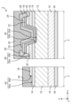
- FIG. 1 is a cross-sectional view of a nitride semiconductor device according to Embodiment 1.
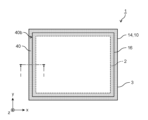
- FIG. FIG. 2 is a plan view of the nitride semiconductor device according to Embodiment 1.
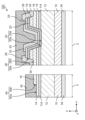
- FIG. 3 is a cross-sectional view of a nitride semiconductor device according to Embodiment 2.
- FIG. 4 is a cross-sectional view of a nitride semiconductor device according to Embodiment 3.
- FIG. FIG. 5 is a cross-sectional view of a nitride semiconductor device according to a fourth embodiment.
- nitride semiconductor device disclosed in Patent Document 1, a highly resistive GaN layer and a p-type GaN layer located on the GaN layer are provided between the source electrode and the drift layer.
- the breakdown voltage is improved by providing the GaN layer with increased resistance.
- an undoped AlGaN layer and a p-type GaN layer located on the undoped AlGaN layer are provided between the source electrode and the drift layer.
- the undoped AlGaN layer generates a two-dimensional electron gas near the interface with the undoped AlGaN layer within the drift layer. As a result, the resistance during operation is reduced by widening the current path in the horizontal direction.
- the inventors of the present application are considering providing grooves penetrating through the p-type GaN layer at the end of the device in such a conventional nitride semiconductor device.
- the p-type GaN layer is prevented from appearing on the facets, and leakage current flowing through the facets can be suppressed.
- the nitride semiconductor device disclosed in Patent Document 2 does not include a high-resistance layer, there is a risk of a decrease in breakdown voltage due to an increase in off-leak during reverse conduction operation.
- a two-dimensional electron gas exists in the drift layer, an electric field tends to concentrate on the end face of the groove, which induces deterioration of off-characteristics.
- a nitride semiconductor device includes a substrate, a first nitride semiconductor layer provided above the substrate, and a semiconductor device provided above the first nitride semiconductor layer.
- a first high-resistance semiconductor layer having a resistance higher than that of the first nitride semiconductor layer; a first p-type nitride semiconductor layer provided above the first high-resistance semiconductor layer; a second high-resistance semiconductor layer having a resistance higher than that of the first nitride semiconductor layer provided above the first p-type nitride semiconductor layer; a first opening that penetrates the p-type nitride semiconductor layer and the first high-resistance semiconductor layer and reaches the first nitride semiconductor layer; an electron transit layer and an electron supply layer provided in order from the bottom so as to cover the first opening; a gate electrode provided above the electron supply layer so as to cover the first opening; a source electrode provided apart from the electrode and in contact with the
- the breakdown voltage can be improved.
- the high resistance AlGaN layer functions as an etching stopper layer when forming the groove. Therefore, the high-resistance AlGaN layer located at the bottom of the groove can be left, and the formation of leakage current paths such as microspikes can be suppressed. Therefore, a decrease in breakdown voltage of the device can be suppressed, and the off characteristics can be improved.
- the nitride semiconductor device includes a second nitride semiconductor layer provided between the first nitride semiconductor layer and the first high-resistance semiconductor layer.
- the second nitride semiconductor layer may be an undoped AlGaN layer.
- a two-dimensional electron gas is generated in the first nitride semiconductor layer near the interface with the undoped AlGaN layer. Since the current can easily spread laterally in the first nitride semiconductor layer, the on-state resistance can be reduced. Since the two-dimensional electron gas in the first nitride semiconductor layer also spreads in the vicinity of the groove, the electric field tends to concentrate on the end faces of the groove. However, since the high-resistance AlGaN layer is arranged on the bottom of the groove, it can withstand a high electric field and improve the breakdown voltage. In this way, it is possible to achieve both improvement in off-characteristics and reduction in on-resistance.
- the insulating film may contain at least Si and N, for example.
- the N vacancies in the nitride semiconductor layer can be terminated, so the occurrence of current collapse can be suppressed.
- the nitride semiconductor device may include a second p-type nitride semiconductor layer provided between the gate electrode and the electron supply layer.
- the second p-type nitride semiconductor layer can reduce the carrier concentration immediately below the gate electrode, and the threshold voltage of the FET can be shifted to the positive side. Therefore, the transistor portion of the nitride semiconductor device can be operated as a normally-off FET.
- the nitride semiconductor device may include a field plate provided above the insulating film so as to protrude into the trench.
- the concentration of the electric field at the termination can be relaxed, and the off characteristics can be further improved.
- the field plate may be electrically connected to the source electrode.
- the concentration of the electric field at the terminal end can be further alleviated, and the OFF characteristics can be further improved.
- each figure is a schematic diagram and is not necessarily strictly illustrated. Therefore, for example, scales and the like do not necessarily match in each drawing. Moreover, in each figure, substantially the same configurations are denoted by the same reference numerals, and overlapping descriptions are omitted or simplified.
- the x-axis, y-axis and z-axis indicate the three axes of a three-dimensional orthogonal coordinate system.
- the x-axis and the y-axis are directions parallel to the first side of the rectangle and the second side orthogonal to the first side, respectively, when the substrate has a rectangular shape in plan view.
- the z-axis is the thickness direction of the substrate.
- the "thickness direction" of the substrate refers to the direction perpendicular to the main surface of the substrate.
- the thickness direction is the same as the stacking direction of the semiconductor layers, and is also referred to as the “longitudinal direction”.
- a direction parallel to the main surface of the substrate may be referred to as a "lateral direction”.
- the side of the substrate on which the gate electrode and the source electrode are provided (the positive side of the z-axis) is regarded as the “upper side” or the “upper side”
- the side of the substrate on which the drain electrode is provided (the negative side of the z-axis) is regarded as the “upper side”. side) as "lower” or "lower”.
- the terms “upper” and “lower” do not refer to the upward direction (vertically upward) and the downward direction (vertically downward) in absolute spatial recognition, but are based on the stacking order in the stacking structure. It is used as a term defined by a relative positional relationship. Also, the terms “above” and “below” are used not only when two components are spaced apart from each other and there is another component between the two components, but also when two components are spaced apart from each other. It also applies when two components are in contact with each other and are placed in close contact with each other.
- planar view means when viewed from a direction perpendicular to the main surface of the substrate of the nitride semiconductor device, that is, when the main surface of the substrate is viewed from the front. .
- ordinal numbers such as “first” and “second” do not mean the number or order of constituent elements unless otherwise specified, so as to avoid confusion between constituent elements of the same kind and to distinguish them from each other. It is used for the purpose of
- AlGaN represents a ternary mixed crystal Al x Ga 1-x N (0 ⁇ x ⁇ 1).
- multi-element mixed crystals are abbreviated by the arrangement of their constituent element symbols, eg, AlInN, GaInN, and the like.
- AlxGa1 -xyInyN ( 0 ⁇ x ⁇ 1, 0 ⁇ y ⁇ 1, and 0 ⁇ x+y ⁇ 1), which is an example of a nitride semiconductor, is abbreviated as AlGaInN.
- FIG. 1 is a cross-sectional view of a nitride semiconductor device 1 according to this embodiment.
- FIG. 2 is a plan view of nitride semiconductor device 1 according to the present embodiment.
- FIG. 1 shows a cross section taken along line II of FIG.
- the transistor portion 2 and the terminal portion 3 are schematically shown separately.
- the nitride semiconductor device 1 includes a transistor portion 2 and a termination portion 3.
- the nitride semiconductor device 1 includes a substrate 10, a drift layer 12, a first high-resistance semiconductor layer 14, a p-type nitride semiconductor layer 16, a second high-resistance semiconductor layer 18, It includes a gate opening 20 , an electron transit layer 22 , an electron supply layer 24 , a source opening 26 , a source electrode 28 , a potential fixing electrode 30 , a gate electrode 32 and a drain electrode 34 .
- Nitride semiconductor device 1 also includes groove portion 40 provided in terminal portion 3 and insulating film 42 provided across transistor portion 2 and terminal portion 3 .
- the transistor section 2 is a region containing FETs, and is a region containing the center of the nitride semiconductor device 1 as shown in FIG. Specifically, the transistor section 2 is a region in which the second high-resistance semiconductor layer 18, the gate opening 20, the electron transit layer 22, the electron supply layer 24, the source electrode 28 or the gate electrode 32 are arranged in plan view. (see Figure 1).
- FIG. 2 illustration of details of each component arranged in the transistor section 2 is omitted.
- a plurality of source electrodes 28 elongated in one direction in plan view are arranged in stripes, and gate electrodes 32 and gate openings 20 are arranged between adjacent source electrodes 28 .
- a plurality of source electrodes 28 having a hexagonal shape in plan view may be arranged so as to be planarly filled with a gap therebetween.
- the terminal portion 3 is a region other than the transistor portion 2 and is provided in a ring shape surrounding the transistor portion 2 .
- the second high-resistance semiconductor layer 18 , gate opening 20 , electron transit layer 22 , electron supply layer 24 , source electrode 28 and gate electrode 32 are not arranged in the terminal portion 3 .
- the nitride semiconductor device 1 is a device having a laminated structure of semiconductor layers mainly composed of nitride semiconductors such as GaN and AlGaN. Specifically, nitride semiconductor device 1 has a heterostructure of an AlGaN film and a GaN film.
- the nitride semiconductor device 1 is a field effect transistor (FET) using a two-dimensional electron gas generated in the electron transit layer 22 as a channel.
- FET field effect transistor
- the nitride semiconductor device 1 is a so-called vertical FET.
- the nitride semiconductor device 1 is a normally-off FET.
- the source electrode 28 is grounded (that is, the potential is 0V), and the drain electrode 34 is given a positive potential.
- the potential applied to the drain electrode 34 is, for example, 100 V or more and 1200 V or less, but is not limited thereto.
- gate electrode 32 is applied with 0V or a negative potential (eg, -5V).
- gate electrode 32 is applied with a positive potential (for example, +5 V).
- Nitride semiconductor device 1 may be a normally-on FET.
- the substrate 10 is a substrate made of a nitride semiconductor.
- the substrate 10 is, for example, a substrate made of n + -type GaN having a thickness of 300 ⁇ m and a donor concentration of 1 ⁇ 10 18 cm ⁇ 3 .
- the top surface of the substrate 10 substantially coincides with the (0001) plane (c-plane) of GaN.
- n-type, n + -type and n - -type, and p-type, p + -type and p - -type indicate conductivity types of semiconductors.
- the n-type, n + -type and n ⁇ -type are examples of the first conductivity type of nitride semiconductors.
- P-type, p.sup. + - type, and p.sup.--type are examples of a second conductivity type that differs in polarity from the first conductivity type.
- the substrate 10 does not have to be a nitride semiconductor substrate.
- the substrate 10 may be a silicon (Si) substrate, a silicon carbide (SiC) substrate, a zinc oxide (ZnO) substrate, or the like.
- Drift layer 12 is an example of a first nitride semiconductor layer provided above substrate 10 .
- the drift layer 12 is, for example, a film made of n ⁇ -type GaN with a thickness of 8 ⁇ m.
- Drift layer 12 is provided in contact with the upper surface of substrate 10 .
- the donor concentration of the drift layer 12 is lower than the donor concentration of the substrate 10, for example, 1 ⁇ 10 15 cm ⁇ 3 or more and 1 ⁇ 10 17 cm ⁇ 3 or less.
- the drift layer 12 may contain carbon (C).
- the carbon concentration of the drift layer 12 is lower than the carbon concentration of the first high-resistance semiconductor layer 14, and is, for example, 1 ⁇ 10 15 cm ⁇ 3 or more and 2 ⁇ 10 17 cm ⁇ 3 or less.
- the first high-resistance semiconductor layer 14 is an example of a first high-resistance semiconductor layer provided above the drift layer 12 .
- the resistance of the first high resistance semiconductor layer 14 is higher than the resistance of the drift layer 12 .
- the thickness of the first high-resistance semiconductor layer 14 is, for example, 200 nm.
- the first high resistance semiconductor layer 14 is provided in contact with the upper surface of the drift layer 12 .
- the first high resistance semiconductor layer 14 is a high resistance AlGaN layer.
- the high-resistance AlGaN layer is a layer containing AlGaN as a main component, and is a layer having a higher resistance than undoped AlGaN due to the presence of a predetermined element.
- "undoped” means that dopants such as Si, O (oxygen), or Mg (magnesium) that change the polarity of the nitride semiconductor to n-type or p-type are not substantially doped.
- the first high-resistance semiconductor layer 14 is an AlGaN layer containing carbon (C).
- the carbon concentration is, for example, 3 ⁇ 10 17 cm ⁇ 3 or more, preferably 1 ⁇ 10 18 cm ⁇ 3 or more.
- the first high-resistance semiconductor layer 14 may be formed by implanting ions such as magnesium (Mg), iron (Fe), or boron (B) into AlGaN. Similar effects can be obtained with ion species other than those described above as long as the ion species used for ion implantation is an ion species capable of increasing the resistance.
- the p-type nitride semiconductor layer 16 is an example of a first p-type nitride semiconductor layer provided above the first high-resistance semiconductor layer 14 .
- the p-type nitride semiconductor layer 16 is, for example, a film made of p ⁇ -type GaN having a thickness of 400 nm and a carrier concentration of 1 ⁇ 10 17 cm ⁇ 3 .
- the p-type nitride semiconductor layer 16 contains, for example, magnesium (Mg) as p-type impurities.
- the p-type nitride semiconductor layer 16 is provided in contact with the upper surface of the first high-resistance semiconductor layer 14 .
- the second high-resistance semiconductor layer 18 is an example of a second high-resistance semiconductor layer provided above the p-type nitride semiconductor layer 16 .
- the resistance of the second high resistance semiconductor layer 18 is higher than the resistance of the drift layer 12 .
- the thickness of the second high resistance semiconductor layer 18 is, for example, 200 nm.
- the second high resistance semiconductor layer 18 is provided in contact with the upper surface of the p-type nitride semiconductor layer 16 .
- the second high resistance semiconductor layer 18 is a high resistance GaN layer.
- the high-resistance GaN layer is a layer containing GaN as a main component and having a higher resistance than undoped GaN due to the presence of a predetermined element.
- the second high-resistance semiconductor layer 18 is a GaN layer containing carbon (C).
- the carbon concentration is, for example, 3 ⁇ 10 17 cm ⁇ 3 or more, preferably 1 ⁇ 10 18 cm ⁇ 3 or more.
- the gate opening 20 is an example of a first opening that penetrates the second high-resistance semiconductor layer 18, the p-type nitride semiconductor layer 16, and the first high-resistance semiconductor layer 14 and reaches the drift layer 12.
- gate opening 20 has a bottom portion 20a and sidewall portions 20b.
- the bottom portion 20 a is the upper surface of the drift layer 12 and is located below the interface between the first high-resistance semiconductor layer 14 and the drift layer 12 .
- Sidewall portion 20 b is an end surface of each of second high-resistance semiconductor layer 18 , p-type nitride semiconductor layer 16 and first high-resistance semiconductor layer 14 and part of the upper surface of drift layer 12 .
- a side wall portion 20 b of the gate opening portion 20 is inclined with respect to the main surface of the substrate 10 .
- the cross-sectional shape of the gate opening 20 is an inverted trapezoid, more specifically, an inverted isosceles trapezoid. Note that the cross-sectional shape of the gate opening 20 may be rectangular.
- the electron transit layer 22 is provided so as to cover the upper surface of the second high-resistance semiconductor layer 18 and the gate opening 20 . Specifically, the electron transit layer 22 is provided in contact with the upper surface of the second high-resistance semiconductor layer 18 and the side wall portion 20b and the bottom portion 20a of the gate opening portion 20, respectively.
- the electron transit layer 22 is a first regrowth layer formed by regrowth of the nitride semiconductor after the gate opening 20 is formed.
- the thickness of the electron transit layer 22 is substantially uniform, and curved along the shape of the inner surface of the gate opening 20 .
- the electron transit layer 22 is, for example, a film made of undoped GaN with a thickness of 100 nm.
- the electron transit layer 22 may be n-type by being doped with Si or the like.
- An AlN layer having a thickness of about 1 nm may be provided as a second regrowth layer between the electron transit layer 22 and the electron supply layer 24 .
- the AlN layer can suppress alloy scattering and improve channel mobility.
- the AlN layer may not be provided, and the electron transit layer 22 and the electron supply layer 24 may be in direct contact.
- a two-dimensional electron gas (not shown) forming a channel is generated near the interface between the AlN layer and the electron transit layer 22 .
- the electron supply layer 24 is provided above the electron transit layer 22 . Specifically, the electron supply layer 24 is provided along the upper surface of the electron transit layer 22 .
- the electron supply layer 24 is a third regrowth layer formed by regrowth of the nitride semiconductor after the gate opening 20 is formed.
- the electron supply layer 24 has a substantially uniform thickness and is curved along the curved shape of the upper surface of the electron transit layer 22 .
- the electron supply layer 24 is, for example, a film made of AlGaN with a thickness of 50 nm.
- the source opening 26 is an example of a second opening that penetrates the second high-resistance semiconductor layer 18 and reaches the p-type nitride semiconductor layer 16 at a position away from the gate electrode 32 . Specifically, the source opening 26 penetrates the electron supply layer 24 , the electron transit layer 22 and the second high-resistance semiconductor layer 18 and reaches the p-type nitride semiconductor layer 16 .
- the source opening 26 has a bottom portion 26a and sidewall portions 26b.
- the bottom portion 26 a is the upper surface of the p-type nitride semiconductor layer 16 and is located below the interface between the p-type nitride semiconductor layer 16 and the second high-resistance semiconductor layer 18 .
- Side wall portion 26 b is an end surface of each of electron supply layer 24 , electron transit layer 22 and second high-resistance semiconductor layer 18 and part of the upper surface of p-type nitride semiconductor layer 16 .
- a side wall portion 26 b of the source opening 26 is obliquely inclined with respect to the main surface of the substrate 10 .
- the cross-sectional shape of the source opening 26 is an inverted trapezoid, more specifically, an inverted isosceles trapezoid. Note that the cross-sectional shape of the source opening 26 may be rectangular.
- the source electrode 28 is provided apart from the gate electrode 32 and is in contact with the electron supply layer 24 and the electron transit layer 22 .
- Source electrode 28 is provided to cover bottom portion 26 a and sidewall portion 26 b of source opening 26 .
- the source electrode 28 is in direct contact with the two-dimensional electron gas in the electron transit layer 22 at the side wall portion 26b of the source opening 26 .
- the source electrode 28 is formed using a conductive material such as metal.
- a material that makes ohmic contact with an n-type semiconductor can be used, such as titanium (Ti).
- Ti titanium
- the source electrode 28 may have a laminated structure of a Ti film and an Al film. In the laminated structure, the Al film is on the lower layer side of the Ti film, and is expressed as Ti/Al in this specification.
- the potential fixing electrode 30 is in contact with the p-type nitride semiconductor layer 16 at the bottom 26 a of the source opening 26 .
- the potential fixing electrode 30 is electrically connected to the source electrode 28 .
- the potential fixing electrode 30 is part of the source electrode 28 .
- the potential fixing electrode 30 can be regarded as a portion of the source electrode 28 that contacts the bottom portion 26 a of the source opening 26 .
- the potential fixing electrode 30 is formed using the same material as the source electrode 28 .
- the gate electrode 32 is provided above the electron supply layer 24 so as to cover the gate opening 20 .
- the gate electrode 32 is shaped along the upper surface of the electron supply layer 24 and is formed in contact with the upper surface of the electron supply layer 24 with a substantially uniform thickness.
- the gate electrode 32 is formed using a conductive material such as metal.
- the gate electrode 32 is formed using Pd.
- a material that makes Schottky contact with an n-type semiconductor can be used, such as a Ni-based material, WSi, Au, or the like.
- the drain electrode 34 is provided below the substrate 10 . Specifically, the drain electrode 34 is provided in contact with the lower surface of the substrate 10 (the surface opposite to the crystal growth surface).
- the drain electrode 34 is formed using a conductive material such as metal.
- the drain electrode 34 can be made of a material that makes ohmic contact with an n-type semiconductor, like the material of the source electrode 28 .
- Each nitride semiconductor layer can be formed by epitaxial growth such as MOVPE (Metal-Organic Vapor Phase Epitaxy) method.
- MOVPE Metal-Organic Vapor Phase Epitaxy
- the drift layer 12, the first high-resistance semiconductor layer 14, the p-type nitride semiconductor layer 16, the second high-resistance semiconductor layer 18, the electron transit layer 22, and the electron supply layer 24 are formed using an MOVPE device.
- MOVPE Metal-Organic Vapor Phase Epitaxy
- the drift layer 12, the first high resistance semiconductor layer 14, the p-type nitride semiconductor layer 16 and the second high resistance semiconductor layer 18 are formed in this order, for example, continuously in the same chamber.
- the electron transit layer 22 and the electron supply layer 24 are continuously formed in the same chamber by crystal regrowth.
- P-type impurities and impurities for increasing resistance can be added to each layer by introducing impurity elements during crystal growth.
- impurities may be added by ion implantation or the like after forming an undoped semiconductor layer.
- Gate opening 20, source opening 26 and trench 40 are formed by photolithography and etching. Etching is, for example, dry etching.
- the source electrode 28, the potential fixing electrode 30, the gate electrode 32 and the drain electrode 34 are each formed by depositing a metal film by vapor deposition or sputtering and patterning it into a predetermined shape. Patterning can be done by photolithography and etching. Note that the drain electrode 34 may be provided on the entire bottom surface of the substrate 10 without being patterned.
- the second high resistance semiconductor layer 18, the electron transit layer 22, the electron supply layer 24, the source electrode 28 and the gate electrode 32 are not provided in the terminal portion 3.
- the second high-resistance semiconductor layer 18, the electron transit layer 22, and the electron supply layer 24 in the termination portion 3 are removed simultaneously with the formation of the source opening portion 26.
- a groove portion 40 is provided in the terminal end portion 3 .
- the groove portion 40 is an isolation trench for partitioning and isolating the transistor portion 2 .
- the groove portion 40 penetrates the p-type nitride semiconductor layer 16 and reaches the first high resistance semiconductor layer 14 .
- a portion of the p-type nitride semiconductor layer 16 is provided at the terminal portion 3 .
- the termination portion 3 includes, in plan view, a region where the p-type nitride semiconductor layer 16 is arranged and a region where the p-type nitride semiconductor layer 16 is not arranged (specifically, the groove portion 40 is provided). area), and
- the groove portion 40 has a bottom portion 40a and side wall portions 40b.
- the groove portion 40 is a stepped portion having sidewall portions 40b only on the transistor portion 2 side. That is, the bottom portion 40a of the groove portion 40 is connected to the end face of the nitride semiconductor device 1. As shown in FIG.
- the groove portion 40 is provided in a ring shape surrounding the transistor portion 2, as shown in FIG.
- a bottom portion 40 a of the groove portion 40 is part of the upper surface of the first high-resistance semiconductor layer 14 .
- the bottom portion 40a is parallel to the upper surface of the substrate 10, for example.
- the groove part 40 is formed so that the opening area is constant regardless of the distance from the substrate 10 .
- the side wall portion 40b of the groove portion 40 is perpendicular to the bottom portion 40a. That is, the cross-sectional shape of the groove portion 40 is rectangular. Note that the cross-sectional shape of the groove portion 40 may be an inverted trapezoid like the gate opening portion 20 .
- the trench 40 is formed, for example, by performing dry etching with a different etching mask following the dry etching process for forming the source opening 26 .
- the trench 40 may be formed by dry etching after forming the source electrode 28 or the potential fixing electrode 30, or after forming the gate electrode 32.
- the first high resistance semiconductor layer 14 is provided between the drift layer 12 and the p-type nitride semiconductor layer 16 . That is, the first high resistance semiconductor layer 14 is inserted into the parasitic pn junction of the parasitic pn diode composed of n-type GaN (drift layer 12) and p-type GaN (p-type nitride semiconductor layer 16). This makes it difficult for current to flow between the p-type nitride semiconductor layer 16 and the drift layer 12 . That is, the current path of the parasitic pn junction diode can be cut off.
- the potential of the p-type nitride semiconductor layer 16 is fixed by the potential fixing electrode 30 .
- the p-type nitride semiconductor layer 16 is fixed to the same potential as the potential of the source electrode 28 (source potential).
- the p-type nitride semiconductor layer 16 functions as a blocking layer that suppresses leak current flowing from the drain electrode 34 toward the source electrode 28 without passing through the channel (two-dimensional electron gas in the electron transit layer 22).
- the p-type nitride semiconductor layer 16 can be separated from the end surface of the nitride semiconductor device 1 by providing the groove portion 40 in the terminal portion 3 . As a result, it is possible to suppress the occurrence of leakage current along the end surface of the device when the device is turned off, and to increase the breakdown voltage.
- the p-type nitride semiconductor layer 16 and the first high resistance semiconductor layer 14 are formed using different materials.
- the p-type nitride semiconductor layer 16 is a p-type GaN layer
- the first high-resistance semiconductor layer 14 is an AlGaN layer to which carbon is added.
- the AlGaN layer functions as a stopper layer against dry etching of the GaN layer. That is, when the p-type nitride semiconductor layer 16 (GaN layer) is removed by dry etching, the first high resistance semiconductor layer 14 (AlGaN layer) remains without being removed.
- the first high-resistance semiconductor layer 14 does not have a local opening or a portion having a small film thickness, a leakage current path between the p-type nitride semiconductor layer 16 and the n-type drift layer 12 is prevented. can be suppressed. As a result, it is possible to suppress the generation of leak current when the device is turned off, and to increase the breakdown voltage.
- the OFF characteristics can be improved.
- the insulating film 42 is provided over the transistor section 2 and the terminal section 3 . Specifically, the insulating film 42 covers the gate electrode 32 and the source electrode 28 and is provided along the inner surfaces (bottom portion 40a and side wall portions 40b) of the trench portion 40 .
- the insulating film 42 is a protective film covering almost the entire nitride semiconductor device 1 .
- the insulating film 42 is formed using an insulating material.
- the insulating film 42 contains silicon (Si) and nitrogen (N).
- Si silicon
- N nitrogen
- the insulating film 42 can terminate the N-holes. Therefore, the deterioration of the film quality of the GaN layer is suppressed, and the occurrence of current collapse can be suppressed.
- the insulating film 42 does not necessarily contain Si and N.
- the insulating film 42 is, for example, a single layer or laminated structure such as a silicon oxide film, a silicon nitride film, a silicon oxynitride film, an aluminum oxide film, or the like.
- the nitride semiconductor device according to Embodiment 2 differs from Embodiment 1 in that it includes a semiconductor layer forming a heterointerface with drift layer 12 .
- the following description focuses on the differences from the first embodiment, and omits or simplifies the description of the common points.
- FIG. 3 is a cross-sectional view of nitride semiconductor device 101 according to the present embodiment.
- nitride semiconductor device 101 includes an electron supply layer 114 in addition to the configuration of nitride semiconductor device 1 shown in FIG.
- the electron supply layer 114 is an example of a second nitride semiconductor layer provided between the drift layer 12 and the first high-resistance semiconductor layer 14 .
- the electron supply layer 114 is, for example, a film made of undoped AlGaN with a thickness of 50 nm.
- the electron supply layer 114 is formed by the MOVPE method following the formation of the drift layer 12 .
- the electron supply layer 114 is arranged in contact with the upper surface of the drift layer 12 and forms an AlGaN/GaN heterointerface with the drift layer 12 . As a result, a two-dimensional electron gas is generated in the drift layer 12 near the interface with the electron supply layer 114 .
- the two-dimensional electron gas in the drift layer 12 extends laterally (specifically, parallel to the upper surface of the substrate 10) from the vicinity of the bottom 20a of the gate opening 20. is formed in Therefore, electrons moving through the two-dimensional electron gas (channel) in the electron transit layer 22 tend to spread laterally through the two-dimensional electron gas in the drift layer 12 in the vicinity of the bottom portion 20a. Therefore, in the drift layer 12, not only the portion positioned immediately below the bottom portion 20a, but also the portion positioned outside the relevant portion (outside the bottom portion 20a in plan view) can be used as a current flow path. Therefore, the source-drain current is easily diffused over a wide region in the drift layer 12 . Therefore, the resistance value during operation of the nitride semiconductor device 101 can be reduced.
- the two-dimensional electron gas in the drift layer 12 also spreads in the vicinity of the groove 40, the electric field tends to concentrate on the end faces of the groove 40.
- the first high-resistance semiconductor layer 14 is arranged in the bottom portion 40a of the groove portion 40, it is possible to withstand a high electric field and improve the breakdown voltage.
- nitride semiconductor device 101 according to the present embodiment it is possible to achieve both improvement in off-state characteristics and reduction in on-state resistance.
- the nitride semiconductor device according to Embodiment 3 differs from Embodiment 1 in that a p-type nitride semiconductor layer is provided between the gate electrode and the electron transit layer.
- the following description focuses on the differences from the first embodiment, and omits or simplifies the description of the common points.
- FIG. 4 is a cross-sectional view of a nitride semiconductor device 201 according to this embodiment.
- nitride semiconductor device 201 includes a p-type nitride semiconductor layer 232 in addition to the configuration of nitride semiconductor device 1 shown in FIG.
- the p-type nitride semiconductor layer 232 is an example of a second p-type nitride semiconductor layer provided between the gate electrode 32 and the electron supply layer 24.
- the p-type nitride semiconductor layer 232 is in contact with the top surface of the electron supply layer 24 and the bottom surface of the gate electrode 32 .
- the p-type nitride semiconductor layer 232 is, for example, a nitride semiconductor layer made of p-type AlGaN having a thickness of 100 nm and a carrier concentration of 1 ⁇ 10 17 cm ⁇ 3 .
- the p-type nitride semiconductor layer 232 is formed by forming a film by the MOVPE method successively from the film formation of the electron supply layer 24 and patterning.
- the p-type nitride semiconductor layer 232 raises the potential of the conduction band edge of the channel portion. Therefore, the threshold voltage of nitride semiconductor device 201 can be increased. That is, the transistor section 2 of the nitride semiconductor device 201 can be operated as a normally-off FET.
- a layer formed using an insulating material such as silicon nitride (SiN) or silicon oxide (SiO 2 ) may be provided instead of the p-type nitride semiconductor layer 232 .
- the material is not particularly limited as long as it has the effect of raising the potential of the channel.
- the nitride semiconductor device 201 may include the electron supply layer 114 as in the second embodiment.
- the nitride semiconductor device according to Embodiment 4 differs from Embodiment 1 in that it includes a field plate.
- the following description focuses on the differences from the first embodiment, and omits or simplifies the description of the common points.
- FIG. 5 is a cross-sectional view of a nitride semiconductor device 301 according to this embodiment.
- nitride semiconductor device 301 includes field plate 344 in addition to the configuration of nitride semiconductor device 1 shown in FIG.
- the nitride semiconductor device 301 includes an insulating film 342 instead of the insulating film 42 .
- the insulating film 342 is provided along the inner surface of the trench 40 .
- the insulating film 342 includes components other than the field plate 344 and the source electrode 28 (specifically, the gate electrode 32, the electron supply layer 24, the p-type nitride semiconductor layer 16, and the first high resistance semiconductor). It is provided to electrically isolate the layer 14 and the drift layer 12).
- the insulating film 342 is formed on the entire upper surface of the gate electrode 32 and the trench 40 after they are formed, and is patterned so as to expose at least part of the source electrode 28 . That is, the insulating film 342 has a contact hole for electrically connecting the source electrode 28 and the field plate 344 .
- the insulating film 342 can be formed using the same material as the insulating film 42, for example.
- the field plate 344 is provided above the insulating film 342 so as to protrude into the groove 40 . That is, the field plate 344 overlaps the bottom portion 40a of the groove portion 40 in plan view.
- the field plate 344 is formed using a conductive material such as metal.
- a conductive material such as metal.
- the same material as the source electrode 28 can be used as the material of the field plate 344 .
- field plate 344 is electrically connected to source electrode 28 . That is, the field plate 344 is supplied with the same potential as the source electrode 28 .
- the electric field in the OFF state tends to concentrate at the intersection between the bottom portion 40 a and the side wall portion 40 b of the groove portion 40 , that is, the corner portion of the groove portion 40 .
- the field plate 344 is provided so as to protrude from the groove 40, part of the electric field concentrated at the intersection of the bottom 40a and the side wall 40b can be dispersed to the protruding portion of the field plate 344. Since a pn junction including etching damage exists in the vicinity of the intersection of the bottom portion 40a and the side wall portion 40b, the off-characteristics of the nitride semiconductor device 301 are improved by alleviating the electric field concentration on the pn junction. can be improved.
- the field plate 344 may be insulated from the source electrode 28 and may be separately supplied with the same potential as the source electrode 28 or a different potential.
- the insulating film 342 is not provided with a contact hole for electrically connecting the source electrode 28 and the field plate 344 .
- the nitride semiconductor device 301 may include the electron supply layer 114 as in the second embodiment. Further, nitride semiconductor device 301 may include p-type nitride semiconductor layer 232 as in the third embodiment.
- the potential fixing electrode 30 is a part of the source electrode 28 was shown, but it is not limited to this.
- the potential fixing electrode 30 and the source electrode 28 may be physically separated.
- the potential fixing electrode 30 and the source electrode 28 can be electrically connected by the field plate 344 provided above the insulating film 342 .
- the potential fixing electrode 30 may be formed using a material different from that of the source electrode 28 .
- a material that makes ohmic contact with the p-type nitride semiconductor layer 16 can be used as the material of the potential fixing electrode 30 .
- a material that makes ohmic contact with the p-type nitride semiconductor layer 16 can be used as the material of the potential fixing electrode 30 .
- palladium (Pd), nickel (Ni), gold (Au), tungsten silicide (WSi), etc. can be used. Since these materials are the same as those used for the gate electrode 32, the gate electrode 32 and the potential fixing electrode 30 can be formed in the same process.
- the source electrode 28 may not be provided within the source opening 26 .
- the source electrode 28 may be arranged on the upper surface of the electron supply layer 24 and may not be in contact with the electron transit layer 22 .
- the source opening 26 is an opening for the potential fixing electrode 30 to come into contact with the p-type nitride semiconductor layer 16 and is provided at a position separated from the source electrode 28 .
- the drift layer 12 may have a graded structure in which the impurity concentration (donor concentration) is gradually reduced from the substrate 10 side to the first high-resistance semiconductor layer 14 side.
- the donor concentration may be controlled by Si as a donor, or by carbon as an acceptor that compensates for Si.
- the drift layer 12 may be composed of a plurality of nitride semiconductor layers with different impurity concentrations.
- the termination portion 3 does not have to include the end surface of the nitride semiconductor device 1 .
- the termination portion 3 is a portion for separating the transistor portion 2 from other devices.
- Another element may be arranged in a region adjacent to the terminal portion 3 of the transistor portion 2 .
- another element is a pn diode using a pn junction between the drift layer 12 and the p-type nitride semiconductor layer 16 .
- the nitride semiconductor device 1 includes a transistor portion 2, a termination portion 3, and a pn diode.
- the present disclosure can be used as a nitride semiconductor device with improved off characteristics, and can be used, for example, in power devices used in power supply circuits of consumer equipment.
Landscapes
- Junction Field-Effect Transistors (AREA)
Priority Applications (2)
| Application Number | Priority Date | Filing Date | Title |
|---|---|---|---|
| JP2023570644A JPWO2023127187A1 (https=) | 2021-12-27 | 2022-07-20 | |
| US18/739,679 US20240332372A1 (en) | 2021-12-27 | 2024-06-11 | Nitride semiconductor device |
Applications Claiming Priority (2)
| Application Number | Priority Date | Filing Date | Title |
|---|---|---|---|
| JP2021-212461 | 2021-12-27 | ||
| JP2021212461 | 2021-12-27 |
Related Child Applications (1)
| Application Number | Title | Priority Date | Filing Date |
|---|---|---|---|
| US18/739,679 Continuation US20240332372A1 (en) | 2021-12-27 | 2024-06-11 | Nitride semiconductor device |
Publications (1)
| Publication Number | Publication Date |
|---|---|
| WO2023127187A1 true WO2023127187A1 (ja) | 2023-07-06 |
Family
ID=86998547
Family Applications (1)
| Application Number | Title | Priority Date | Filing Date |
|---|---|---|---|
| PCT/JP2022/028179 Ceased WO2023127187A1 (ja) | 2021-12-27 | 2022-07-20 | 窒化物半導体デバイス |
Country Status (3)
| Country | Link |
|---|---|
| US (1) | US20240332372A1 (https=) |
| JP (1) | JPWO2023127187A1 (https=) |
| WO (1) | WO2023127187A1 (https=) |
Citations (5)
| Publication number | Priority date | Publication date | Assignee | Title |
|---|---|---|---|---|
| WO2015004853A1 (ja) * | 2013-07-12 | 2015-01-15 | パナソニックIpマネジメント株式会社 | 半導体装置 |
| JP2015023074A (ja) * | 2013-07-17 | 2015-02-02 | 豊田合成株式会社 | 半導体装置 |
| WO2019187789A1 (ja) * | 2018-03-27 | 2019-10-03 | パナソニック株式会社 | 窒化物半導体装置 |
| WO2021070469A1 (ja) * | 2019-10-09 | 2021-04-15 | パナソニック株式会社 | 窒化物半導体デバイス |
| WO2021140898A1 (ja) * | 2020-01-08 | 2021-07-15 | パナソニック株式会社 | 窒化物半導体装置 |
-
2022
- 2022-07-20 JP JP2023570644A patent/JPWO2023127187A1/ja active Pending
- 2022-07-20 WO PCT/JP2022/028179 patent/WO2023127187A1/ja not_active Ceased
-
2024
- 2024-06-11 US US18/739,679 patent/US20240332372A1/en active Pending
Patent Citations (5)
| Publication number | Priority date | Publication date | Assignee | Title |
|---|---|---|---|---|
| WO2015004853A1 (ja) * | 2013-07-12 | 2015-01-15 | パナソニックIpマネジメント株式会社 | 半導体装置 |
| JP2015023074A (ja) * | 2013-07-17 | 2015-02-02 | 豊田合成株式会社 | 半導体装置 |
| WO2019187789A1 (ja) * | 2018-03-27 | 2019-10-03 | パナソニック株式会社 | 窒化物半導体装置 |
| WO2021070469A1 (ja) * | 2019-10-09 | 2021-04-15 | パナソニック株式会社 | 窒化物半導体デバイス |
| WO2021140898A1 (ja) * | 2020-01-08 | 2021-07-15 | パナソニック株式会社 | 窒化物半導体装置 |
Also Published As
| Publication number | Publication date |
|---|---|
| US20240332372A1 (en) | 2024-10-03 |
| JPWO2023127187A1 (https=) | 2023-07-06 |
Similar Documents
| Publication | Publication Date | Title |
|---|---|---|
| US20230207636A1 (en) | High Voltage Blocking III-V Semiconductor Device | |
| JP6161910B2 (ja) | 半導体装置 | |
| US7816707B2 (en) | Field-effect transistor with nitride semiconductor and method for fabricating the same | |
| US9589951B2 (en) | High-electron-mobility transistor with protective diode | |
| CN102292801B (zh) | 场效应晶体管及其制造方法 | |
| JP7303807B2 (ja) | 窒化物半導体装置 | |
| CN111902920B (zh) | 氮化物半导体装置 | |
| US20140110759A1 (en) | Semiconductor device | |
| JP7813766B2 (ja) | 窒化物半導体デバイス | |
| KR101982402B1 (ko) | 반도체 장치와 그 제조 방법 | |
| CN104704615B (zh) | 开关元件 | |
| JP7361723B2 (ja) | 窒化物半導体装置 | |
| US20250275170A1 (en) | Nitride semiconductor device | |
| US20200312964A1 (en) | Nitride semiconductor device | |
| CN114270532B (zh) | 半导体装置及其制造方法 | |
| WO2023042617A1 (ja) | 半導体装置 | |
| US12289899B2 (en) | Nitride-based semiconductor device and method for manufacturing the same | |
| JP2013239735A (ja) | 電界効果トランジスタ | |
| US20240313061A1 (en) | Nitride semiconductor device | |
| WO2023127187A1 (ja) | 窒化物半導体デバイス | |
| US12527023B2 (en) | Nitride semiconductor device | |
| US20250287681A1 (en) | Nitride semiconductor device and method for manufacturing the nitride semiconductor device | |
| US20260082611A1 (en) | Nitride semiconductor device | |
| JP2023133798A (ja) | 窒化物半導体デバイス | |
| JP2025125348A (ja) | 窒化物半導体デバイス |
Legal Events
| Date | Code | Title | Description |
|---|---|---|---|
| 121 | Ep: the epo has been informed by wipo that ep was designated in this application |
Ref document number: 22915422 Country of ref document: EP Kind code of ref document: A1 |
|
| WWE | Wipo information: entry into national phase |
Ref document number: 2023570644 Country of ref document: JP |
|
| NENP | Non-entry into the national phase |
Ref country code: DE |
|
| 122 | Ep: pct application non-entry in european phase |
Ref document number: 22915422 Country of ref document: EP Kind code of ref document: A1 |