WO2023119726A1 - Procédé de traitement de substrat, procédé de production de dispositif à semi-conducteur, appareil de traitement de substrat et programme - Google Patents
Procédé de traitement de substrat, procédé de production de dispositif à semi-conducteur, appareil de traitement de substrat et programme Download PDFInfo
- Publication number
- WO2023119726A1 WO2023119726A1 PCT/JP2022/031498 JP2022031498W WO2023119726A1 WO 2023119726 A1 WO2023119726 A1 WO 2023119726A1 JP 2022031498 W JP2022031498 W JP 2022031498W WO 2023119726 A1 WO2023119726 A1 WO 2023119726A1
- Authority
- WO
- WIPO (PCT)
- Prior art keywords
- film
- bonds
- ratio
- substrate
- substrate processing
- Prior art date
Links
- 238000012545 processing Methods 0.000 title claims abstract description 282
- 239000000758 substrate Substances 0.000 title claims abstract description 121
- 238000003672 processing method Methods 0.000 title claims abstract description 19
- 239000004065 semiconductor Substances 0.000 title claims description 17
- 238000004519 manufacturing process Methods 0.000 title claims description 13
- 229910010271 silicon carbide Inorganic materials 0.000 claims abstract description 41
- 229910018540 Si C Inorganic materials 0.000 claims abstract description 38
- 238000010438 heat treatment Methods 0.000 claims abstract description 27
- 229910007991 Si-N Inorganic materials 0.000 claims abstract description 19
- 229910006294 Si—N Inorganic materials 0.000 claims abstract description 19
- 239000002994 raw material Substances 0.000 claims description 52
- 238000000034 method Methods 0.000 claims description 50
- 239000003054 catalyst Substances 0.000 claims description 47
- 230000008569 process Effects 0.000 claims description 34
- 229910052739 hydrogen Inorganic materials 0.000 claims description 25
- 229910052799 carbon Inorganic materials 0.000 claims description 23
- 239000007800 oxidant agent Substances 0.000 claims description 23
- 229910052760 oxygen Inorganic materials 0.000 claims description 16
- 230000007246 mechanism Effects 0.000 claims description 14
- 238000009832 plasma treatment Methods 0.000 claims description 14
- 229910052710 silicon Inorganic materials 0.000 claims description 14
- 229910052757 nitrogen Inorganic materials 0.000 claims description 11
- 239000005046 Chlorosilane Substances 0.000 claims description 5
- 230000008021 deposition Effects 0.000 claims description 5
- 239000012528 membrane Substances 0.000 claims description 5
- KOPOQZFJUQMUML-UHFFFAOYSA-N chlorosilane Chemical compound Cl[SiH3] KOPOQZFJUQMUML-UHFFFAOYSA-N 0.000 claims description 4
- 229910052734 helium Inorganic materials 0.000 claims description 4
- 239000010408 film Substances 0.000 description 227
- 239000007789 gas Substances 0.000 description 161
- 235000012431 wafers Nutrition 0.000 description 120
- 238000012546 transfer Methods 0.000 description 36
- 239000011261 inert gas Substances 0.000 description 35
- 238000004380 ashing Methods 0.000 description 29
- 239000000460 chlorine Substances 0.000 description 25
- 238000000137 annealing Methods 0.000 description 23
- 238000003860 storage Methods 0.000 description 18
- 238000010926 purge Methods 0.000 description 16
- QGZKDVFQNNGYKY-UHFFFAOYSA-N Ammonia Chemical compound N QGZKDVFQNNGYKY-UHFFFAOYSA-N 0.000 description 12
- ZMANZCXQSJIPKH-UHFFFAOYSA-N Triethylamine Chemical compound CCN(CC)CC ZMANZCXQSJIPKH-UHFFFAOYSA-N 0.000 description 12
- 239000001257 hydrogen Substances 0.000 description 12
- 238000011144 upstream manufacturing Methods 0.000 description 12
- 230000015572 biosynthetic process Effects 0.000 description 11
- 239000012495 reaction gas Substances 0.000 description 11
- 229910052801 chlorine Inorganic materials 0.000 description 10
- 230000001590 oxidative effect Effects 0.000 description 10
- IJGRMHOSHXDMSA-UHFFFAOYSA-N Atomic nitrogen Chemical compound N#N IJGRMHOSHXDMSA-UHFFFAOYSA-N 0.000 description 9
- QVGXLLKOCUKJST-UHFFFAOYSA-N atomic oxygen Chemical compound [O] QVGXLLKOCUKJST-UHFFFAOYSA-N 0.000 description 9
- 239000001301 oxygen Substances 0.000 description 9
- KRHYYFGTRYWZRS-UHFFFAOYSA-N Fluorane Chemical compound F KRHYYFGTRYWZRS-UHFFFAOYSA-N 0.000 description 8
- UFHFLCQGNIYNRP-UHFFFAOYSA-N Hydrogen Chemical compound [H][H] UFHFLCQGNIYNRP-UHFFFAOYSA-N 0.000 description 8
- 230000000694 effects Effects 0.000 description 8
- 239000000126 substance Substances 0.000 description 8
- 229910000040 hydrogen fluoride Inorganic materials 0.000 description 7
- 239000012535 impurity Substances 0.000 description 7
- 238000010586 diagram Methods 0.000 description 6
- 239000000872 buffer Substances 0.000 description 5
- OKTJSMMVPCPJKN-UHFFFAOYSA-N Carbon Chemical compound [C] OKTJSMMVPCPJKN-UHFFFAOYSA-N 0.000 description 4
- MWUXSHHQAYIFBG-UHFFFAOYSA-N Nitric oxide Chemical compound O=[N] MWUXSHHQAYIFBG-UHFFFAOYSA-N 0.000 description 4
- 238000004140 cleaning Methods 0.000 description 4
- 230000003028 elevating effect Effects 0.000 description 4
- 150000002431 hydrogen Chemical class 0.000 description 4
- 125000002887 hydroxy group Chemical group [H]O* 0.000 description 4
- 239000007788 liquid Substances 0.000 description 4
- 229910000069 nitrogen hydride Inorganic materials 0.000 description 4
- 230000003647 oxidation Effects 0.000 description 4
- 238000007254 oxidation reaction Methods 0.000 description 4
- XLYOFNOQVPJJNP-UHFFFAOYSA-N water Chemical compound O XLYOFNOQVPJJNP-UHFFFAOYSA-N 0.000 description 4
- BLRPTPMANUNPDV-UHFFFAOYSA-N Silane Chemical compound [SiH4] BLRPTPMANUNPDV-UHFFFAOYSA-N 0.000 description 3
- XUIMIQQOPSSXEZ-UHFFFAOYSA-N Silicon Chemical compound [Si] XUIMIQQOPSSXEZ-UHFFFAOYSA-N 0.000 description 3
- 150000001412 amines Chemical class 0.000 description 3
- 238000006243 chemical reaction Methods 0.000 description 3
- 230000006870 function Effects 0.000 description 3
- 229910052736 halogen Inorganic materials 0.000 description 3
- 150000002367 halogens Chemical class 0.000 description 3
- 239000001307 helium Substances 0.000 description 3
- SWQJXJOGLNCZEY-UHFFFAOYSA-N helium atom Chemical compound [He] SWQJXJOGLNCZEY-UHFFFAOYSA-N 0.000 description 3
- 125000004435 hydrogen atom Chemical group [H]* 0.000 description 3
- 229910000077 silane Inorganic materials 0.000 description 3
- 239000010703 silicon Substances 0.000 description 3
- SYSHGEHAYJKOLC-UHFFFAOYSA-N 1,1,3,3-tetrachloro-1,3-disiletane Chemical compound Cl[Si]1(Cl)C[Si](Cl)(Cl)C1 SYSHGEHAYJKOLC-UHFFFAOYSA-N 0.000 description 2
- OISVCGZHLKNMSJ-UHFFFAOYSA-N 2,6-dimethylpyridine Chemical compound CC1=CC=CC(C)=N1 OISVCGZHLKNMSJ-UHFFFAOYSA-N 0.000 description 2
- -1 Alkylene chlorosilane Chemical compound 0.000 description 2
- XKRFYHLGVUSROY-UHFFFAOYSA-N Argon Chemical compound [Ar] XKRFYHLGVUSROY-UHFFFAOYSA-N 0.000 description 2
- CURLTUGMZLYLDI-UHFFFAOYSA-N Carbon dioxide Chemical compound O=C=O CURLTUGMZLYLDI-UHFFFAOYSA-N 0.000 description 2
- GQPLMRYTRLFLPF-UHFFFAOYSA-N Nitrous Oxide Chemical compound [O-][N+]#N GQPLMRYTRLFLPF-UHFFFAOYSA-N 0.000 description 2
- CBENFWSGALASAD-UHFFFAOYSA-N Ozone Chemical compound [O-][O+]=O CBENFWSGALASAD-UHFFFAOYSA-N 0.000 description 2
- GLUUGHFHXGJENI-UHFFFAOYSA-N Piperazine Chemical compound C1CNCCN1 GLUUGHFHXGJENI-UHFFFAOYSA-N 0.000 description 2
- NQRYJNQNLNOLGT-UHFFFAOYSA-N Piperidine Chemical compound C1CCNCC1 NQRYJNQNLNOLGT-UHFFFAOYSA-N 0.000 description 2
- JUJWROOIHBZHMG-UHFFFAOYSA-N Pyridine Chemical compound C1=CC=NC=C1 JUJWROOIHBZHMG-UHFFFAOYSA-N 0.000 description 2
- 229910021529 ammonia Inorganic materials 0.000 description 2
- 238000004891 communication Methods 0.000 description 2
- JTBAMRDUGCDKMS-UHFFFAOYSA-N dichloro-[dichloro(methyl)silyl]-methylsilane Chemical compound C[Si](Cl)(Cl)[Si](C)(Cl)Cl JTBAMRDUGCDKMS-UHFFFAOYSA-N 0.000 description 2
- HPNMFZURTQLUMO-UHFFFAOYSA-N diethylamine Chemical compound CCNCC HPNMFZURTQLUMO-UHFFFAOYSA-N 0.000 description 2
- 125000004805 propylene group Chemical group [H]C([H])([H])C([H])([*:1])C([H])([H])[*:2] 0.000 description 2
- 239000000376 reactant Substances 0.000 description 2
- 230000000717 retained effect Effects 0.000 description 2
- 239000000243 solution Substances 0.000 description 2
- 125000006850 spacer group Chemical group 0.000 description 2
- JHFNJRVFKOQALR-UHFFFAOYSA-N 1-prop-2-enylpyrrole Chemical compound C=CCN1C=CC=C1 JHFNJRVFKOQALR-UHFFFAOYSA-N 0.000 description 1
- BSKHPKMHTQYZBB-UHFFFAOYSA-N 2-methylpyridine Chemical compound CC1=CC=CC=N1 BSKHPKMHTQYZBB-UHFFFAOYSA-N 0.000 description 1
- IVSPVXKJEGPQJP-UHFFFAOYSA-N 2-silylethylsilane Chemical compound [SiH3]CC[SiH3] IVSPVXKJEGPQJP-UHFFFAOYSA-N 0.000 description 1
- MGWGWNFMUOTEHG-UHFFFAOYSA-N 4-(3,5-dimethylphenyl)-1,3-thiazol-2-amine Chemical compound CC1=CC(C)=CC(C=2N=C(N)SC=2)=C1 MGWGWNFMUOTEHG-UHFFFAOYSA-N 0.000 description 1
- NUKYPUAOHBNCPY-UHFFFAOYSA-N 4-aminopyridine Chemical compound NC1=CC=NC=C1 NUKYPUAOHBNCPY-UHFFFAOYSA-N 0.000 description 1
- ZCYVEMRRCGMTRW-UHFFFAOYSA-N 7553-56-2 Chemical compound [I] ZCYVEMRRCGMTRW-UHFFFAOYSA-N 0.000 description 1
- VHUUQVKOLVNVRT-UHFFFAOYSA-N Ammonium hydroxide Chemical compound [NH4+].[OH-] VHUUQVKOLVNVRT-UHFFFAOYSA-N 0.000 description 1
- WKBOTKDWSSQWDR-UHFFFAOYSA-N Bromine atom Chemical compound [Br] WKBOTKDWSSQWDR-UHFFFAOYSA-N 0.000 description 1
- UGFAIRIUMAVXCW-UHFFFAOYSA-N Carbon monoxide Chemical compound [O+]#[C-] UGFAIRIUMAVXCW-UHFFFAOYSA-N 0.000 description 1
- ZAMOUSCENKQFHK-UHFFFAOYSA-N Chlorine atom Chemical compound [Cl] ZAMOUSCENKQFHK-UHFFFAOYSA-N 0.000 description 1
- PXGOKWXKJXAPGV-UHFFFAOYSA-N Fluorine Chemical compound FF PXGOKWXKJXAPGV-UHFFFAOYSA-N 0.000 description 1
- 101000735417 Homo sapiens Protein PAPPAS Proteins 0.000 description 1
- MHAJPDPJQMAIIY-UHFFFAOYSA-N Hydrogen peroxide Chemical compound OO MHAJPDPJQMAIIY-UHFFFAOYSA-N 0.000 description 1
- BIVNKSDKIFWKFA-UHFFFAOYSA-N N-propan-2-yl-N-silylpropan-2-amine Chemical compound CC(C)N([SiH3])C(C)C BIVNKSDKIFWKFA-UHFFFAOYSA-N 0.000 description 1
- 102100034919 Protein PAPPAS Human genes 0.000 description 1
- 229910008051 Si-OH Inorganic materials 0.000 description 1
- 229910003923 SiC 4 Inorganic materials 0.000 description 1
- 229910003902 SiCl 4 Inorganic materials 0.000 description 1
- 229910006358 Si—OH Inorganic materials 0.000 description 1
- XMIJDTGORVPYLW-UHFFFAOYSA-N [SiH2] Chemical compound [SiH2] XMIJDTGORVPYLW-UHFFFAOYSA-N 0.000 description 1
- VOSJXMPCFODQAR-UHFFFAOYSA-N ac1l3fa4 Chemical compound [SiH3]N([SiH3])[SiH3] VOSJXMPCFODQAR-UHFFFAOYSA-N 0.000 description 1
- 230000004913 activation Effects 0.000 description 1
- 150000003927 aminopyridines Chemical class 0.000 description 1
- 235000011114 ammonium hydroxide Nutrition 0.000 description 1
- 239000007864 aqueous solution Substances 0.000 description 1
- 229910052786 argon Inorganic materials 0.000 description 1
- GDTBXPJZTBHREO-UHFFFAOYSA-N bromine Substances BrBr GDTBXPJZTBHREO-UHFFFAOYSA-N 0.000 description 1
- 229910052794 bromium Inorganic materials 0.000 description 1
- 239000001569 carbon dioxide Substances 0.000 description 1
- 229910002092 carbon dioxide Inorganic materials 0.000 description 1
- 230000003197 catalytic effect Effects 0.000 description 1
- 239000007809 chemical reaction catalyst Substances 0.000 description 1
- 239000003795 chemical substances by application Substances 0.000 description 1
- GJCAUTWJWBFMFU-UHFFFAOYSA-N chloro-dimethyl-trimethylsilylsilane Chemical compound C[Si](C)(C)[Si](C)(C)Cl GJCAUTWJWBFMFU-UHFFFAOYSA-N 0.000 description 1
- GPTXWRGISTZRIO-UHFFFAOYSA-N chlorquinaldol Chemical compound ClC1=CC(Cl)=C(O)C2=NC(C)=CC=C21 GPTXWRGISTZRIO-UHFFFAOYSA-N 0.000 description 1
- 238000005520 cutting process Methods 0.000 description 1
- 125000004122 cyclic group Chemical group 0.000 description 1
- 238000000354 decomposition reaction Methods 0.000 description 1
- 230000006837 decompression Effects 0.000 description 1
- MROCJMGDEKINLD-UHFFFAOYSA-N dichlorosilane Chemical compound Cl[SiH2]Cl MROCJMGDEKINLD-UHFFFAOYSA-N 0.000 description 1
- UCXUKTLCVSGCNR-UHFFFAOYSA-N diethylsilane Chemical compound CC[SiH2]CC UCXUKTLCVSGCNR-UHFFFAOYSA-N 0.000 description 1
- 238000009792 diffusion process Methods 0.000 description 1
- HPYNZHMRTTWQTB-UHFFFAOYSA-N dimethylpyridine Natural products CC1=CC=CN=C1C HPYNZHMRTTWQTB-UHFFFAOYSA-N 0.000 description 1
- UBHZUDXTHNMNLD-UHFFFAOYSA-N dimethylsilane Chemical compound C[SiH2]C UBHZUDXTHNMNLD-UHFFFAOYSA-N 0.000 description 1
- 235000012489 doughnuts Nutrition 0.000 description 1
- 238000005530 etching Methods 0.000 description 1
- 238000011066 ex-situ storage Methods 0.000 description 1
- 230000005284 excitation Effects 0.000 description 1
- 230000005281 excited state Effects 0.000 description 1
- 229910052731 fluorine Inorganic materials 0.000 description 1
- 239000011737 fluorine Substances 0.000 description 1
- QOSATHPSBFQAML-UHFFFAOYSA-N hydrogen peroxide;hydrate Chemical compound O.OO QOSATHPSBFQAML-UHFFFAOYSA-N 0.000 description 1
- 230000001771 impaired effect Effects 0.000 description 1
- 238000011065 in-situ storage Methods 0.000 description 1
- 230000001939 inductive effect Effects 0.000 description 1
- 229910052740 iodine Inorganic materials 0.000 description 1
- 239000011630 iodine Substances 0.000 description 1
- 238000005468 ion implantation Methods 0.000 description 1
- 238000010030 laminating Methods 0.000 description 1
- 239000000463 material Substances 0.000 description 1
- 238000005259 measurement Methods 0.000 description 1
- 239000003595 mist Substances 0.000 description 1
- 239000000203 mixture Substances 0.000 description 1
- 230000004048 modification Effects 0.000 description 1
- 238000012986 modification Methods 0.000 description 1
- OWKFQWAGPHVFRF-UHFFFAOYSA-N n-(diethylaminosilyl)-n-ethylethanamine Chemical compound CCN(CC)[SiH2]N(CC)CC OWKFQWAGPHVFRF-UHFFFAOYSA-N 0.000 description 1
- VYIRVGYSUZPNLF-UHFFFAOYSA-N n-(tert-butylamino)silyl-2-methylpropan-2-amine Chemical compound CC(C)(C)N[SiH2]NC(C)(C)C VYIRVGYSUZPNLF-UHFFFAOYSA-N 0.000 description 1
- SSCVMVQLICADPI-UHFFFAOYSA-N n-methyl-n-[tris(dimethylamino)silyl]methanamine Chemical compound CN(C)[Si](N(C)C)(N(C)C)N(C)C SSCVMVQLICADPI-UHFFFAOYSA-N 0.000 description 1
- 229910052754 neon Inorganic materials 0.000 description 1
- GKAOGPIIYCISHV-UHFFFAOYSA-N neon atom Chemical compound [Ne] GKAOGPIIYCISHV-UHFFFAOYSA-N 0.000 description 1
- JCXJVPUVTGWSNB-UHFFFAOYSA-N nitrogen dioxide Inorganic materials O=[N]=O JCXJVPUVTGWSNB-UHFFFAOYSA-N 0.000 description 1
- 239000001272 nitrous oxide Substances 0.000 description 1
- 230000003287 optical effect Effects 0.000 description 1
- 230000002093 peripheral effect Effects 0.000 description 1
- QQONPFPTGQHPMA-UHFFFAOYSA-N propylene Natural products CC=C QQONPFPTGQHPMA-UHFFFAOYSA-N 0.000 description 1
- UMJSCPRVCHMLSP-UHFFFAOYSA-N pyridine Natural products COC1=CC=CN=C1 UMJSCPRVCHMLSP-UHFFFAOYSA-N 0.000 description 1
- 239000010453 quartz Substances 0.000 description 1
- 150000003254 radicals Chemical class 0.000 description 1
- 238000011084 recovery Methods 0.000 description 1
- 238000006057 reforming reaction Methods 0.000 description 1
- 230000004044 response Effects 0.000 description 1
- FZHAPNGMFPVSLP-UHFFFAOYSA-N silanamine Chemical compound [SiH3]N FZHAPNGMFPVSLP-UHFFFAOYSA-N 0.000 description 1
- VYPSYNLAJGMNEJ-UHFFFAOYSA-N silicon dioxide Inorganic materials O=[Si]=O VYPSYNLAJGMNEJ-UHFFFAOYSA-N 0.000 description 1
- FDNAPBUWERUEDA-UHFFFAOYSA-N silicon tetrachloride Chemical compound Cl[Si](Cl)(Cl)Cl FDNAPBUWERUEDA-UHFFFAOYSA-N 0.000 description 1
- 239000007787 solid Substances 0.000 description 1
- 238000001179 sorption measurement Methods 0.000 description 1
- 239000010409 thin film Substances 0.000 description 1
- WDVUXWDZTPZIIE-UHFFFAOYSA-N trichloro(2-trichlorosilylethyl)silane Chemical compound Cl[Si](Cl)(Cl)CC[Si](Cl)(Cl)Cl WDVUXWDZTPZIIE-UHFFFAOYSA-N 0.000 description 1
- LXEXBJXDGVGRAR-UHFFFAOYSA-N trichloro(trichlorosilyl)silane Chemical compound Cl[Si](Cl)(Cl)[Si](Cl)(Cl)Cl LXEXBJXDGVGRAR-UHFFFAOYSA-N 0.000 description 1
- ABDDAHLAEXNYRC-UHFFFAOYSA-N trichloro(trichlorosilylmethyl)silane Chemical compound Cl[Si](Cl)(Cl)C[Si](Cl)(Cl)Cl ABDDAHLAEXNYRC-UHFFFAOYSA-N 0.000 description 1
- PZKOFHKJGUNVTM-UHFFFAOYSA-N trichloro-[dichloro(trichlorosilyl)silyl]silane Chemical compound Cl[Si](Cl)(Cl)[Si](Cl)(Cl)[Si](Cl)(Cl)Cl PZKOFHKJGUNVTM-UHFFFAOYSA-N 0.000 description 1
- FAQYAMRNWDIXMY-UHFFFAOYSA-N trichloroborane Chemical compound ClB(Cl)Cl FAQYAMRNWDIXMY-UHFFFAOYSA-N 0.000 description 1
- PQDJYEQOELDLCP-UHFFFAOYSA-N trimethylsilane Chemical compound C[SiH](C)C PQDJYEQOELDLCP-UHFFFAOYSA-N 0.000 description 1
- GIRKRMUMWJFNRI-UHFFFAOYSA-N tris(dimethylamino)silicon Chemical compound CN(C)[Si](N(C)C)N(C)C GIRKRMUMWJFNRI-UHFFFAOYSA-N 0.000 description 1
- 239000012808 vapor phase Substances 0.000 description 1
- 238000001039 wet etching Methods 0.000 description 1
- 229910052724 xenon Inorganic materials 0.000 description 1
- FHNFHKCVQCLJFQ-UHFFFAOYSA-N xenon atom Chemical compound [Xe] FHNFHKCVQCLJFQ-UHFFFAOYSA-N 0.000 description 1
Images


Classifications
-
- C—CHEMISTRY; METALLURGY
- C23—COATING METALLIC MATERIAL; COATING MATERIAL WITH METALLIC MATERIAL; CHEMICAL SURFACE TREATMENT; DIFFUSION TREATMENT OF METALLIC MATERIAL; COATING BY VACUUM EVAPORATION, BY SPUTTERING, BY ION IMPLANTATION OR BY CHEMICAL VAPOUR DEPOSITION, IN GENERAL; INHIBITING CORROSION OF METALLIC MATERIAL OR INCRUSTATION IN GENERAL
- C23C—COATING METALLIC MATERIAL; COATING MATERIAL WITH METALLIC MATERIAL; SURFACE TREATMENT OF METALLIC MATERIAL BY DIFFUSION INTO THE SURFACE, BY CHEMICAL CONVERSION OR SUBSTITUTION; COATING BY VACUUM EVAPORATION, BY SPUTTERING, BY ION IMPLANTATION OR BY CHEMICAL VAPOUR DEPOSITION, IN GENERAL
- C23C16/00—Chemical coating by decomposition of gaseous compounds, without leaving reaction products of surface material in the coating, i.e. chemical vapour deposition [CVD] processes
- C23C16/22—Chemical coating by decomposition of gaseous compounds, without leaving reaction products of surface material in the coating, i.e. chemical vapour deposition [CVD] processes characterised by the deposition of inorganic material, other than metallic material
- C23C16/30—Deposition of compounds, mixtures or solid solutions, e.g. borides, carbides, nitrides
- C23C16/42—Silicides
-
- C—CHEMISTRY; METALLURGY
- C23—COATING METALLIC MATERIAL; COATING MATERIAL WITH METALLIC MATERIAL; CHEMICAL SURFACE TREATMENT; DIFFUSION TREATMENT OF METALLIC MATERIAL; COATING BY VACUUM EVAPORATION, BY SPUTTERING, BY ION IMPLANTATION OR BY CHEMICAL VAPOUR DEPOSITION, IN GENERAL; INHIBITING CORROSION OF METALLIC MATERIAL OR INCRUSTATION IN GENERAL
- C23C—COATING METALLIC MATERIAL; COATING MATERIAL WITH METALLIC MATERIAL; SURFACE TREATMENT OF METALLIC MATERIAL BY DIFFUSION INTO THE SURFACE, BY CHEMICAL CONVERSION OR SUBSTITUTION; COATING BY VACUUM EVAPORATION, BY SPUTTERING, BY ION IMPLANTATION OR BY CHEMICAL VAPOUR DEPOSITION, IN GENERAL
- C23C16/00—Chemical coating by decomposition of gaseous compounds, without leaving reaction products of surface material in the coating, i.e. chemical vapour deposition [CVD] processes
- C23C16/56—After-treatment
-
- H—ELECTRICITY
- H01—ELECTRIC ELEMENTS
- H01L—SEMICONDUCTOR DEVICES NOT COVERED BY CLASS H10
- H01L21/00—Processes or apparatus adapted for the manufacture or treatment of semiconductor or solid state devices or of parts thereof
- H01L21/02—Manufacture or treatment of semiconductor devices or of parts thereof
- H01L21/04—Manufacture or treatment of semiconductor devices or of parts thereof the devices having potential barriers, e.g. a PN junction, depletion layer or carrier concentration layer
- H01L21/18—Manufacture or treatment of semiconductor devices or of parts thereof the devices having potential barriers, e.g. a PN junction, depletion layer or carrier concentration layer the devices having semiconductor bodies comprising elements of Group IV of the Periodic Table or AIIIBV compounds with or without impurities, e.g. doping materials
- H01L21/30—Treatment of semiconductor bodies using processes or apparatus not provided for in groups H01L21/20 - H01L21/26
- H01L21/31—Treatment of semiconductor bodies using processes or apparatus not provided for in groups H01L21/20 - H01L21/26 to form insulating layers thereon, e.g. for masking or by using photolithographic techniques; After treatment of these layers; Selection of materials for these layers
Definitions
- the present disclosure relates to a substrate processing method, a semiconductor device manufacturing method, a substrate processing apparatus, and a program.
- a process of forming a film on a substrate is sometimes performed as one step of the manufacturing process of a semiconductor device (for example, Patent Document 1).
- the present disclosure provides a technique capable of improving the properties of a film formed on a substrate (for example, Patent Document 1).
- a first film including at least one of C—H bonds and Si—C bonds and N—H bonds and Si—N bonds;
- the ratio of Si--C bonds to C--H bonds in the first film is made larger than the ratio of Si--C bonds to C--H bonds in the third film, or the ratio of Si--N bonds to N--H bonds in the third film is set to be greater than the ratio of Si-- to N--H bonds in the first film. and increasing the N-bond ratio.
- FIG. 1 is a cross-sectional view schematically showing a configuration example of a substrate processing unit 2000 preferably used in one aspect of the present disclosure.
- FIG. 2 is a schematic configuration diagram of the controller 121 of the substrate processing unit 2000 preferably used in one aspect of the present disclosure, and is a block diagram showing the control system of the controller 121.
- FIG. 3 is a side sectional view schematically showing a configuration example of a film forming apparatus 300 preferably used in one aspect of the present disclosure.
- FIG. 4 is a side sectional view schematically showing a configuration example of an annealing apparatus 400 preferably used in one aspect of the present disclosure.
- FIG. 5 is a side sectional view schematically showing a configuration example of a plasma processing apparatus 500 preferably used in one aspect of the present disclosure.
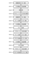
- FIG. 6 is a flow diagram illustrating substrate processing steps in one aspect of the present disclosure.
- FIG. 7 is a diagram illustrating a processing sequence in one aspect of the present disclosure;
- FIG. 8 is a diagram showing measurement results in Examples.
- FIG. 1 to 7 One aspect of the present disclosure will be described mainly with reference to FIGS. 1 to 7.
- FIG. The drawings used in the following description are all schematic, and the dimensional relationship of each element, the ratio of each element, etc. shown in the drawings do not necessarily match the actual ones. Moreover, the dimensional relationship of each element, the ratio of each element, etc. do not necessarily match between a plurality of drawings.
- a substrate processing unit 2000 exemplified in this embodiment is used in a manufacturing process of a semiconductor device, and is configured to perform predetermined processing on a substrate to be processed.
- Substrates to be processed include, for example, semiconductor wafer substrates (hereinafter simply referred to as "wafers") on which semiconductor integrated circuit devices (semiconductor devices) are built.
- wafer substrates hereinafter simply referred to as "wafers”
- semiconductor integrated circuit devices semiconductor integrated circuit devices
- wafer surface when used in this specification, it may mean “the surface (exposed surface) of the wafer itself” or “the surface of a predetermined layer or film formed on the wafer. , that is, the outermost surface of the wafer as a laminate".
- substrate in this specification is synonymous with the use of the term "wafer”.
- the processing performed on the wafer includes, for example, transfer processing, pressurization (decompression) processing, heat processing, film formation processing, modification processing, diffusion processing, carrier activation after ion implantation, and planarization. There are reflow, annealing, etc.
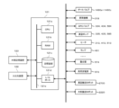
- the substrate processing unit 2000 processes a wafer 200 as a substrate, and includes a film formation device 300, a heat treatment device 400 (also referred to as an annealing device 400), and a plasma processing device 500. It is a so-called cluster-type device configured as follows. More specifically, the substrate processing unit 2000 includes an IO stage 2100, an atmospheric transfer chamber 2200, a load lock (L/L) chamber 2300, a vacuum transfer chamber 2400, a film formation device 300, an annealing device 400, and a plasma processing device 500. configured as follows. In the drawings, the front, rear, left, and right are defined as the X1 direction to the right, the X2 direction to the left, the Y1 direction to the front, and the Y2 direction to the rear.
- An IO stage (load port) 2100 is installed on the front side of the substrate processing unit 100 .
- a plurality of storage containers (hereinafter simply referred to as "pods") 2001 called FOUPs (Front Open Unified Pods) are mounted on the IO stage 2100.
- the pod 2001 is used as a carrier for transporting the wafers 200, and is configured such that a plurality of unprocessed wafers 200 or processed wafers 200 are stored therein in a horizontal posture.
- the IO stage 2100 is adjacent to the atmosphere transfer chamber 2200.
- An atmospheric transfer robot 2220 for transferring the wafer 200 is installed in the atmospheric transfer chamber 2200 .
- a load lock chamber 2300 is connected to the atmosphere transfer chamber 2200 on the side different from the IO stage 2100 .
- a vacuum transfer chamber (transfer module: TM) 2400 is connected to the load lock chamber 2300 on the side different from the atmospheric transfer chamber 2200 .
- the TM2400 functions as a transfer chamber that serves as a transfer space in which the wafer 200 is transferred under negative pressure.
- a housing 2410 constituting the TM 2400 is connected with a film forming apparatus 300, an annealing apparatus 400, and a plasma processing apparatus 500 for processing the wafer 200, respectively.
- a vacuum transfer robot 2700 that transfers the wafer 200 under negative pressure is installed at substantially the center of the TM2400.
- a vacuum transfer robot 2700 installed in the TM2400 has two independently operable arms 2800 and 2900.
- Gate valves (GV) 1490a, GV1490b, and GV1490c are provided between the TM2400 and the film forming apparatus 300, between the TM2400 and the annealing apparatus 400, and between the TM2400 and the plasma processing apparatus 500, respectively.
- the vacuum transfer robot 2700 in the TM 2400 moves the wafer 200 through the substrate loading/unloading ports 350, 450, 550 provided in the film forming apparatus 300, the annealing apparatus 400, and the plasma processing apparatus 500, respectively. can be taken in and out (see FIGS. 3, 4, and 5).
- the controller 121 which is a control unit (control means), is configured as a computer comprising a CPU (Central Processing Unit) 121a, a RAM (Random Access Memory) 121b, a storage device 121c, and an I/O port 121d. It is The RAM 121b, storage device 121c, and I/O port 121d are configured to exchange data with the CPU 121a via an internal bus 121e.
- An input/output device 122 configured as, for example, a touch panel or the like is connected to the controller 121 .
- an external storage device 123 can be connected to the controller 121 .
- the controller 121 controls processing operations of the substrate processing unit 2000 including the film forming device 300, the annealing device 400, and the plasma processing device 500.
- the storage device 121c is composed of, for example, flash memory, HDD (Hard Disk Drive), SSD (Solid State Drive), and the like.
- a control program for controlling the operation of the substrate processing apparatus, a process recipe describing procedures and conditions for substrate processing, which will be described later, and the like are stored in a readable manner.
- the process recipe functions as a program in which the controller 121 causes the substrate processing apparatus to execute each procedure in substrate processing, which will be described later, so as to obtain a predetermined result.
- process recipes, control programs, and the like are collectively referred to simply as programs.
- a process recipe is also simply referred to as a recipe.
- the RAM 121b is configured as a memory area (work area) in which programs and data read by the CPU 121a are temporarily held.
- the I/O port 121d includes the above-described gate valves 1490a to 1490c, the vacuum transfer robot 2700, the atmospheric transfer robot 2220, a lifting mechanism 318, APC valves 334, 434, 584, vacuum pumps 335, 435, 585, and a heater 313, which will be described later. , 413, 513, the lamp 416, the frequency matching device 574, the high frequency power source 573, and the like.
- the CPU 121a is configured to be able to read and execute a control program from the storage device 121c, and read recipes from the storage device 121c in response to input of operation commands from the input/output device 122, and the like.
- the CPU 121a opens and closes the gate valves 1490a to 1490c, the lifting mechanism 318, the vacuum transfer robot 2700, the atmosphere transfer robot 2220, and the APC valves 334, 434, and 584 in accordance with the content of the read recipe.
- the controller 121 can be configured by installing the above-described program stored in the external storage device 123 in the computer.
- the external storage device 123 includes, for example, a magnetic disk such as an HDD, an optical disk such as a CD, a magneto-optical disk such as an MO, a semiconductor memory such as a USB memory or an SSD, and the like.
- the storage device 121c and the external storage device 123 are configured as computer-readable recording media. Hereinafter, these are also collectively referred to simply as recording media.
- recording medium may include only the storage device 121c alone, may include only the external storage device 123 alone, or may include both of them.
- the program may be provided to the computer using communication means such as the Internet or a dedicated line without using the external storage device 123 .
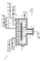
- the film forming apparatus 300 is used when performing a film forming process, which is one step in the manufacturing process of a semiconductor device, and is configured as, for example, a single substrate processing apparatus.
- the film forming apparatus 300 has a processing container 302 .
- a processing chamber 301 for processing the wafer 200 is formed in the processing container 302 .
- a substrate loading/unloading port 350 adjacent to the GV 1490 a is provided on the side surface of the processing vessel 302 , and the wafer 200 is configured to move between the TM 2400 via the substrate loading/unloading port 350 .
- a lift pin 307 is provided at the bottom of the processing container 202 .
- a susceptor 310 as a substrate mounting portion for mounting the wafer 200 is arranged in the processing chamber 301 .
- a substrate mounting surface 311 on which the wafer 200 is mounted is provided on the upper surface of the susceptor 310 .
- a heater 313 is embedded in the susceptor 310 as a heating mechanism for adjusting the temperature of the wafer 200 on the substrate mounting surface 311 .
- a temperature adjustment unit 315 is connected to the heater 313 to adjust the power supplied thereto. The temperature adjuster 315 is controlled according to instructions from the controller 121 .
- the susceptor 310 is provided with through holes 314 through which the lift pins 307 pass, at positions corresponding to the lift pins 307 .
- the susceptor 310 is supported by a shaft 317.
- the shaft 317 penetrates the bottom of the processing container 302 and is connected to an elevating mechanism 318 outside the processing container 302 .
- the periphery of the lower end of the shaft 317 is covered with a bellows 319, and the inside of the processing chamber 301 is kept airtight.
- Gas introduction holes 360 , 370 , and 380 for supplying various gases into the processing chamber 301 are provided in the upper portion of the processing chamber 301 .
- the configuration of the gas supply system connected to the gas introduction holes 360, 370, 380 will be described later.
- a raw material (gas) supply pipe 361a, a catalyst supply pipe 371a, and a reaction gas supply pipe 381a are connected to the gas introduction holes 360, 370, and 380, respectively.
- a raw material (details will be described later) is mainly supplied from a raw material (gas) supply system 361 including a raw material supply pipe 361a.
- a catalyst (details will be described later) is mainly supplied from a catalyst supply system 371 including a catalyst supply pipe 371a.
- a reaction gas is mainly supplied from a reaction gas supply system 381 including a reaction gas supply pipe 381a.
- the raw material supply pipe 361a is provided with, in order from the upstream direction, a raw material (gas) supply source 361b, a mass flow controller (MFC) 361c as a flow controller (flow control unit), and a valve 361d as an on-off valve. .
- a raw material (gas) supply source 361b a raw material (gas) supply source 361b
- MFC mass flow controller
- valve 361d a valve 361d as an on-off valve.
- the downstream end of the first inert gas supply pipe 362a is connected to the downstream side of the valve 361d of the raw material supply pipe 361a.
- the first inert gas supply pipe 362a is provided with an inert gas supply source 362b, an MFC 362c, and a valve 362d in order from the upstream direction.
- the catalyst supply pipe 371a is provided with a catalyst supply source 371b, an MFC 371c, and a valve 371d in this order from the upstream direction.
- the downstream end of the second inert gas supply pipe 372a is connected to the downstream side of the valve 371d of the catalyst supply pipe 371a.
- the second inert gas supply pipe 372a is provided with a second inert gas supply source 372b, an MFC 372c, and a valve 372d in order from the upstream direction.
- the reactant gas supply pipe 381a is provided with a reactant gas supply source 381b, an MFC 381c, and a valve 381d in order from the upstream direction.
- the downstream end of the third inert gas supply pipe 382a is connected to the downstream side of the valve 381d of the reaction gas supply pipe 381a.
- the third inert gas supply pipe 382a is provided with a third inert gas supply source 382b, an MFC 382c, and a valve 382d in order from the upstream direction.
- the raw material (gas), reaction gas, and catalyst gas are also referred to as film-forming gas, either individually or collectively.
- the raw material supply system 361, the catalyst supply system 371, and the reaction gas supply system 381 are also referred to individually or collectively as a film formation gas supply system.
- An exhaust port 345 for exhausting the atmosphere in the processing chamber 301 is provided on the inner wall side surface of the processing container 302 .
- An exhaust pipe 333 is connected to the outer wall side surface of the processing container 302 so as to communicate with the exhaust port 345 .
- the exhaust pipe 333 is provided with an APC (Auto Pressure Controller) valve 334 as a pressure regulator (pressure regulator) and a vacuum pump 335 as an evacuation device in order from the upstream side.
- APC Auto Pressure Controller
- the exhaust port 355, the exhaust pipe 333, and the APC valve 334 are collectively called an exhaust system.
- the annealing apparatus 400 is used for heat treatment (also referred to as annealing treatment), which is one step in the manufacturing process of a semiconductor device, and is configured as, for example, a single substrate processing apparatus.
- heat treatment also referred to as annealing treatment
- the annealing apparatus 400 has a processing container 402 .
- a processing chamber 401 for processing the wafer 200 is formed in the processing container 402 .
- a substrate loading/unloading port 450 adjacent to the GV 1490 b is provided on the side surface of the processing container 402 , and the wafer 200 is configured to move between the TM 2400 via the substrate loading/unloading port 450 .
- a lift pin 407 is provided at the bottom of the processing container 402 .
- a susceptor 410 as a substrate mounting portion for mounting the wafer 200 is arranged in the processing chamber 401 .
- a substrate mounting surface 411 on which the wafer 200 is mounted is provided on the upper surface of the susceptor 410 .
- a heater 413 is embedded in the susceptor 410 as a heating mechanism for adjusting the temperature of the wafer 200 on the substrate mounting surface 411 .
- a heater control unit 420 that controls the temperature of the heater 413 is connected to the heater 413 .
- a heater control unit 420 controls the on/off of the heater 413 based on instructions from the controller 121 .
- the susceptor 310 is provided with through holes 314 through which the lift pins 307 pass, at positions corresponding to the lift pins 307 .
- the susceptor 410 is supported by a shaft 417.
- the shaft 417 passes through the bottom of the processing container 402 and is connected to an elevating mechanism 418 outside the processing container 402 .
- the lower end of the shaft 417 is covered with a bellows 419 so that the inside of the processing chamber 401 is kept airtight.
- a lamp house 460 is provided on the ceiling of the processing container 402 and at a position facing the surface of the wafer 200 .
- a lamp house 460 is provided with a plurality of lamps 461 as heating mechanisms.
- the lamp 461 is connected to the lamp controller 463 via wiring 462 .
- a lamp controller 463 controls the on/off of the lamp 461 based on instructions from the controller 121 .
- a window 464 is provided on the ceiling of the processing container 402 and at a position facing the lamp 461 .
- the window 464 is made of a vacuum-resistant material, such as quartz, which does not block the heat emitted from the lamp 461 .
- a gas introduction hole 440 for supplying an inert gas into the processing chamber 401 is provided in the upper portion of the processing chamber 401 .
- An inert gas supply pipe 441 a is connected to the gas introduction hole 440 .
- An inert gas (details will be described later) is supplied from an inert gas supply system 441 including an inert gas supply pipe 441a.
- the inert gas supply pipe 441a is provided with an inert gas supply source 441b, an MFC 441c, and a valve 441d in order from the upstream direction.
- An exhaust port 445 for exhausting the atmosphere in the processing chamber 401 is provided on the inner wall side surface of the processing container 402 .
- An exhaust pipe 433 is connected to the outer wall side surface of the processing container 402 so as to communicate with the exhaust port 445 .
- the exhaust pipe 433 is provided with an APC valve 434 as a pressure regulator (pressure regulator) and a vacuum pump 435 as an evacuation device in order from the upstream side.
- the exhaust port 455, the exhaust pipe 433, and the APC valve 434 are collectively called an exhaust system.
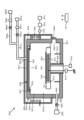
- FIG. 5 is a schematic configuration diagram of a plasma processing apparatus 500 according to this embodiment.
- the plasma processing apparatus 500 includes a processing furnace 502 that accommodates the wafer 200 and performs plasma processing.
- the processing furnace 502 includes a processing container 503 forming a processing chamber 501 .
- the processing container 503 includes an upper container 530 and a lower container 531 .
- a processing chamber 501 is formed by covering the lower container 531 with the upper container 530 .
- a substrate loading/unloading port 550 adjacent to the GV 1490 c is provided on the lower sidewall of the lower container 531 , and the wafer 200 is configured to move between the TM 2400 via the substrate loading/unloading port 580 .
- a lift pin 507 is provided at the bottom of the processing container 503 .
- the processing chamber 501 has a plasma generation space 501a around which a resonance coil 522 is provided, and a substrate processing space 501b communicating with the plasma generation space 501a and in which the wafer 200 is processed.
- the plasma generation space 501 a is a space in which plasma is generated, and refers to the space above the lower end of the resonance coil 522 and below the upper end of the resonance coil 522 in the processing chamber 501 .
- the substrate processing space 501b is a space in which the wafer 200 is processed using plasma and is a space below the lower end of the resonance coil 522 .
- a susceptor 510 as a substrate mounting portion for mounting the wafer 200 is arranged in the processing chamber 501 .
- a substrate mounting surface 511 on which the wafer 200 is mounted is provided on the upper surface of the susceptor 510 .
- a heater 513 is embedded inside the susceptor 510 as a heating mechanism for adjusting the temperature of the wafer 200 on the substrate mounting surface 511 .
- the surface of the wafer 200 can be heated to a predetermined degree within the range of 25.degree. C. to 1000.degree.
- the susceptor 510 is electrically insulated from the lower container 531 .
- An impedance adjustment electrode 515 is provided inside the susceptor 510 .
- the impedance adjustment electrode 515 is grounded through an impedance variable mechanism 577 as an impedance adjustment section. Via the impedance adjusting electrode 515 and the susceptor 510, it is possible to control the potential (bias voltage) of the wafer 200 during plasma processing.
- a susceptor elevating mechanism 568 for elevating the susceptor is provided below the susceptor 510 .
- a through hole 514 is provided in the susceptor 510 .
- a lift pin 507 as a support for supporting the wafer 200 is provided on the bottom surface of the lower container 531 . When the susceptor 510 is lowered by the susceptor lifting mechanism 568 , the lift pins 507 pass through the through holes 514 without contacting the susceptor 510 . This allows the wafer 200 to be held from below.
- a gas supply head 536 is provided above the processing chamber 501 , that is, above the upper container 530 .
- the gas supply head 536 includes a lid 533 , a gas introduction hole 534 , a buffer chamber 537 , an opening 538 , a shield plate 540 and a gas outlet 539 so as to supply gas into the processing chamber 501 . It is configured.
- a hydrogen (H)-containing gas supply pipe 561 a is connected to the gas introduction hole 543 .
- a hydrogen-containing gas (details will be described later) is mainly supplied from an H-containing gas supply system, which will be described later.
- the H-containing gas supply pipe 561a is provided with an H-containing gas supply source 561b, an MFC 561c, and a valve 561d, which is an on-off valve, in this order from the upstream direction.
- the downstream end of the fourth inert gas supply pipe 562a is connected to the downstream side of the valve 561d of the H-containing gas supply pipe 561a.
- the fourth inert gas supply pipe 562a is provided with an inert gas supply source 562b, an MFC 562c, and a valve 562d in this order from the upstream direction.
- An exhaust port 595 for exhausting the atmosphere in the processing chamber 501 is provided on the inner wall side surface of the lower container 531 .
- An exhaust pipe 583 is connected to the outer wall side surface of the lower container 531 so as to communicate with the exhaust port 595 .
- the exhaust pipe 583 is provided with an APC valve 584 as a pressure regulator (pressure regulator) and a vacuum pump 585 as an evacuation device in this order from the upstream side.
- APC valve 584 as a pressure regulator (pressure regulator) and a vacuum pump 585 as an evacuation device in this order from the upstream side.
- the exhaust port 595, the exhaust pipe 583, and the APC valve 584 are collectively called an exhaust system.
- a spiral resonance coil 522 is provided on the outer periphery of the processing chamber 501 , that is, on the outside of the side wall of the upper container 530 so as to surround the processing chamber 501 .
- An RF (Radio Frequency) sensor 572, a high frequency power supply 573, and a frequency matching box 574 (frequency control unit) are connected to the resonance coil 522.
- FIG. A shield plate 223 is provided on the outer peripheral side of the resonance coil 212 .
- a first film is formed on a wafer 200 as a substrate in the film forming apparatus 300 , and a first film is formed in the annealing apparatus 400 .
- a heat treatment is performed on the film to modify the first film into a second film, and plasma processing is performed on the second film in the plasma processing apparatus 500 to modify the second film into a third film.
- FIG. 6 and 7. An example of a substrate processing sequence will be described mainly with reference to FIGS. 6 and 7.
- the controller 121 controls the operation of each component of the substrate processing unit 2000 .
- the substrate processing sequence in this aspect includes: forming a first film on the wafer 200 including at least one of C—H bonds and Si—C bonds and N—H bonds and Si—N bonds; a step b of performing a heat treatment on the first film at a processing temperature higher than the processing temperature in step a to reform the first film into a second film; Plasma treatment is performed on the second film to modify the second film into a third film, and the ratio of Si—C bonds to C—H bonds in the third film is The ratio of Si--C bonds to C--H bonds is greater than the ratio of Si--N bonds to N--H bonds in the third film, or the ratio of Si--N bonds to N--H bonds in the first film is and c.
- step a a raw material containing at least a C—H bond and a Si—C bond and a catalyst are supplied to the wafer 200;
- SiOC film silicon oxycarbide film
- a SiOC film is a Low-k film with a low dielectric constant and is an insulating film with high resistance to hydrogen fluoride (HF) etching (hereinafter referred to as HF resistance), so it is widely used as, for example, a spacer film.
- HF resistance hydrogen fluoride
- the SiOC film may be exposed to oxidation treatment such as oxygen (O 2 ) plasma ashing after film formation as one step of the manufacturing process of the semiconductor device.
- the ashing process deteriorates the HF resistance of the SiOC film, and as a result, the function as a spacer film may be impaired.
- a SiOC film that maintains both a low dielectric constant and a high HF resistance even when subjected to an ashing process after film formation will be described.
- the HF resistance of the film after the ashing process is sometimes referred to as ashing resistance.
- a wafer 200 to be processed is taken out from the pod 2001 on the IO stage 2100 by the atmosphere transfer robot 2220 .
- the GV 1490 a is opened and the wafer 200 is transferred from the TM 2400 into the processing chamber 301 by the vacuum transfer robot 2700 .
- the wafer 200 loaded into the processing chamber 301 is horizontally supported on lift pins 307 projecting upward from the substrate mounting surface 311 of the susceptor 310 .
- the vacuum transfer robot 2700 is withdrawn from the processing chamber 301 and the GV 1490a is closed.
- the susceptor 310 is raised to a predetermined processing position, and the wafer 200 to be processed is transferred from the lift pins 307 onto the susceptor 310 .
- the inside of the processing chamber 301 is evacuated by the vacuum pump 335 so as to have a desired processing pressure.
- the pressure inside the processing chamber 301 is measured by a pressure sensor, and the APC valve 334 is feedback-controlled based on this measured pressure information.
- the wafer 200 is heated by the heater 313 so as to reach a desired processing temperature.
- step a the following steps a1 and a2 are executed.
- step a1 a raw material (raw material gas) and a catalyst (catalyst gas) are supplied as film-forming agents to the wafer 200 in the processing chamber 301 .
- valves 361d and 371d are opened to flow the raw material and the catalyst into the raw material supply pipe 361a and the catalyst supply pipe 371a, respectively.
- the raw material and the catalyst are adjusted in flow rate by the MFCs 361 d and 371 d respectively, supplied into the processing chamber 301 via the buffer chamber 343 , mixed in the processing chamber 301 , and exhausted from the exhaust port 345 .
- the raw material and the catalyst are supplied to the wafer 200 from above the wafer 200 (raw material+catalyst supply).
- valves 362d, 372d, and 382d are opened to supply the inert gas into the processing chamber 301 through the raw material supply pipe 361a, the catalyst supply pipe 371a, and the reaction gas supply pipe 381a, respectively. It should be noted that the supply of inert gas may not be implemented in some of the methods described below.
- the processing conditions for supplying the raw material and the catalyst in this step (step a1) are as follows: Treatment temperature: room temperature (25°C) to 120°C, preferably room temperature to 90°C Processing pressure: 133-1333Pa
- Treatment temperature room temperature (25°C) to 120°C, preferably room temperature to 90°C
- Processing pressure 133-1333Pa
- Raw material supply flow rate 0.001 to 2 slm
- Catalyst supply flow rate 0.001 to 2 slm
- Each gas supply time 1 to 60 seconds is exemplified.
- the expression of a numerical range such as “25 to 120°C” in this specification means that the lower limit and upper limit are included in the range. Therefore, for example, "450 to 750°C” means “450°C to 750°C”.
- the processing temperature in this specification means the temperature of the wafer 200 or the temperature inside the processing chamber 301
- the processing pressure means the pressure inside the processing chamber 301 .
- 0 slm when included in the supply flow rate, 0 slm means a case where the gas is not supplied.
- a silicon (Si)-containing layer containing C, H and Cl is formed as the first layer.
- a Si-containing layer containing C, H and Cl becomes a layer containing C--H bonds and Si--C bonds.
- the Si-containing layer containing C, H and Cl is also simply referred to as the Si-containing layer containing C or the SiC layer for the sake of convenience.
- the first layer includes not only a continuous layer made of Si and containing C, H and Cl, but also a discontinuous layer and a Si thin film containing C, H and Cl formed by stacking these layers.
- Si constituting the Si layer containing C, H and Cl includes not only those whose bonds with C and Cl are not completely broken but also those whose bonds with C and Cl are completely broken.
- the above-described reaction can proceed under the non-plasma atmosphere and under the above-described low temperature conditions.
- the raw material in the processing chamber 301 is thermally decomposed (vapor phase decomposition), that is, it is prevented from self-decomposing. can be This makes it possible to adsorb the raw material on the wafer 200 and form an adsorption layer of the raw material.
- the valves 361d and 371d are closed to stop the supply of raw material and catalyst into the processing chamber 301. Then, the inside of the processing chamber 301 is evacuated to remove gas and the like remaining in the processing chamber 301 from the inside of the processing chamber 301 . At this time, the valves 362 d , 372 d and 382 d are left open to maintain the supply of the inert gas into the processing chamber 301 .
- the inert gas acts as a purge gas, thereby purging the inside of the processing chamber 301 .
- a silane-based gas containing Si as a main element constituting a film formed on the wafer 200 can be used.
- a silane-based gas for example, a gas containing Si and halogen, that is, a halosilane-based gas can be used.
- Halogen includes chlorine (Cl), fluorine (F), bromine (Br), iodine (I), and the like.
- the halosilane-based gas for example, the above-described chlorosilane-based gas containing Si and Cl can be used.
- raw materials include bis(trichlorosilyl)methane ((SiCl 3 ) 2 CH 2 , abbreviation: BTCSM) gas, 1,2-bis(trichlorosilyl)ethane ((SiCl 3 ) 2 C 2 H 4 , abbreviation: Alkylene chlorosilane-based gas such as BTCSE) gas can be used.
- Raw materials include, for example, 1,1,2,2-tetrachloro-1,2-dimethyldisilane ((CH 3 ) 2 Si 2 Cl 4 , abbreviation: TCDMDS) gas, 1,2-dichloro-1,1,
- TCDMDS 1,1,2,2-tetrachloro-1,2-dimethyldisilane
- DCTMDS 2,2-tetramethyldisilane
- a cyclic structure composed of Si and C such as 1,1,3,3-tetrachloro-1,3-disilacyclobutane (C 2 H 4 Cl 4 Si 2 , abbreviation: TCDSCB) gas and A gas containing halogen can be used.
- TCDSCB 1,1,3,3-tetrachloro-1,3-disilacyclobutane
- a gas containing C--H bonds and Si--C bonds as the raw material.
- a gas containing C--H bonds and Si--C bonds can be used as the raw material.
- an amine-based gas containing carbon (C), nitrogen (N), and H can be used.
- amine-based gases include pyridine ( Py) gas, aminopyridine (C5H6N2) gas, picoline (C6H7N ) gas , lutidine (C7H9N ) gas, piperazine ( C4 Cyclic amine-based gases such as H 10 N 2 ) gas and piperidine (C 5 H 11 N) gas, triethylamine ((C 2 H 5 ) 3 N, abbreviation: TEA) gas, diethylamine ((C 2 H 5 ) 2
- a chain amine-based gas such as NH (abbreviation: DEA) gas can be used.
- ammonia (NH 3 ) gas or the like can also be used as the catalyst. One or more of these can be used as the catalyst. This point also applies to step a2, which will be described later.
- a gas containing Si and H and containing at least one element of C and N as the film forming gas (raw material, catalyst).
- the inert gas examples include nitrogen (N 2 ) gas, rare gas such as argon (Ar) gas, helium (He) gas, neon (Ne) gas, and xenon (Xe) gas.
- nitrogen (N 2 ) gas examples include nitrogen (N 2 ) gas, rare gas such as argon (Ar) gas, helium (He) gas, neon (Ne) gas, and xenon (Xe) gas.
- nitrogen (N 2 ) gas examples include nitrogen (N 2 ) gas, rare gas such as argon (Ar) gas, helium (He) gas, neon (Ne) gas, and xenon (Xe) gas.
- Ar argon
- He helium
- Ne neon
- Xe xenon
- Step a2 After step a1 is finished, an oxidizing agent (oxidizing gas) and a catalyst (catalytic gas) are supplied to the wafer 200 in the processing chamber 201, that is, the Si-containing layer formed on the wafer 200.
- oxidizing agent oxidizing gas
- a catalyst catalytic gas
- valves 381d and 371d are opened to flow the oxidizing agent and the catalyst into the reaction gas supply pipe 381a and the catalyst supply pipe 371a, respectively.
- the oxidizing agent and the catalyst are adjusted in flow rate by the MFCs 381 d and 371 d respectively, supplied into the processing chamber 301 through the buffer chamber 343 , mixed in the processing chamber 301 , and exhausted from the exhaust port 345 .
- an oxidant and a catalyst are supplied to the wafer 200 from above the wafer 200 (oxidant+catalyst supply).
- the valves 362 d , 372 d and 382 d are left open to maintain the supply of the inert gas into the processing chamber 301 .
- the processing conditions for supplying the oxidizing agent and the catalyst in this step are as follows: Treatment temperature: room temperature (25°C) to 120°C, preferably room temperature to 100°C Oxidant supply flow rate: 0.001 to 2 slm Catalyst supply flow rate: 0.001 to 2 slm are exemplified. Other processing conditions are the same as the processing conditions in step a1.
- a silicon oxycarbide layer SiOC layer
- impurities such as Cl contained in the first layer form a gaseous substance containing at least Cl in the course of the reforming reaction, and are discharged from the processing chamber 301 .
- the second layer becomes a layer containing fewer impurities such as Cl than the first layer formed in step a1.
- the second layer formed is a layer containing moisture, that is, OH groups.
- step a1 similarly to step a1, by supplying a catalyst together with an oxidizing agent, the above-described reaction can proceed in a non-plasma atmosphere and under low temperature conditions as described later. Become.
- the valves 381d and 371d are closed to stop the supply of the oxidant into the processing chamber 301. Then, the inside of the processing chamber 301 is evacuated to remove gas and the like remaining in the processing chamber 301 from the inside of the processing chamber 301 . At this time, gas or the like remaining in the processing chamber 301 is removed from the processing chamber 301 (purge) by the same processing procedure as the purge in step a1.
- an oxygen (O)-containing gas or an oxygen (O) and hydrogen (H)-containing gas can be used.
- O-containing gas examples include oxygen (O 2 ) gas, ozone (O 3 ) gas, nitrous oxide (N 2 O) gas, nitrogen monoxide (NO) gas, nitrogen dioxide (NO 2 ) gas, and monoxide gas.
- Carbon (CO) gas, carbon dioxide (CO 2 ) gas, or the like can be used.
- the O and H containing gas include water vapor (H 2 O gas), hydrogen peroxide (H 2 O 2 ), hydrogen (H 2 ) gas + oxygen (O 2 ) gas, H 2 gas + ozone (O 3 ) gas or the like can also be used.
- the O- and H-containing gas is also an O-containing gas.
- a cleaning liquid for example, a cleaning liquid containing ammonia water, hydrogen peroxide water, and pure water may be used. That is, oxidation may be performed by APM cleaning. In this case, the oxidation can be performed by exposing the wafer 200 to a cleaning solution.
- the oxidizing agent may be a gaseous substance or a liquid substance.
- the oxidizing agent may be a liquid substance such as a mist substance. One or more of these can be used as the oxidizing agent.
- a predetermined film thickness is formed on the wafer 200 as the first film. of Si, O, and C can be formed.
- the above cycle is preferably repeated multiple times. That is, the thickness of the second layer (SiOC layer) formed per cycle is made thinner than the desired film thickness, and the thickness of the SiOC film as the first film formed by laminating the second layer
- the above cycle is preferably repeated multiple times until the desired thickness is achieved.
- step a by performing step a under the above conditions, the first film (SiOC It is possible to incorporate (remain) in the membrane) as it is.
- the first film (SiOC film) formed on the wafer 200 becomes a film containing water, that is, OH groups on its surface.
- the susceptor 310 is lowered to a predetermined transfer position, and the wafer 200 is transferred from the susceptor 310 onto the lift pins 307 .
- the GV 1490a is opened, and the vacuum transfer robot 2700 unloads the processed wafer 200 out of the processing vessel 302 (TM 2400).
- Heat treatment annealing treatment: S402
- the wafer 200 in the processing chamber 401 is heated to heat-treat the first film (SiOC film) formed on the wafer 200 .
- the valve 441d is opened to flow the inert gas into the inert gas supply pipe 441a.
- the flow rate of the inert gas is adjusted by the MFC 441 c, supplied into the processing chamber 401 and exhausted from the exhaust port 445 .
- inert gas is supplied to the wafer 200 from above the wafer 200 .
- Treatment temperature 200-1000°C, preferably 500-700°C
- Processing pressure 133-1333Pa
- Inert gas supply flow rate 0.001 to 20 slm
- Inert gas supply time 1 to 120 minutes, preferably 1 to 60 minutes.
- the processing temperature in this step is set to a relatively high processing temperature, for example, higher than the processing temperature in the above-described film formation processing (step a), so that the Impurities such as moisture (OH groups present on the surface of the first film) and Cl can be efficiently eliminated.
- a second film is formed on the wafer 200 by desorbing impurities such as moisture and Cl from the first film.
- the second film is made a Low-k film with a lower dielectric constant than the first film, or the second film is changed to the first film. It is possible to maintain a Low-k film with a low dielectric constant similar to that of .
- the H gas is excited to a plasma state and supplied to the wafer 200 in the processing chamber 501 , that is, the second film formed on the wafer 200 .
- valve 561d is opened to allow the H gas to flow into the gas supply pipe 561a.
- the H gas is adjusted in flow rate by the MFC 561c, supplied into the processing chamber 501 through the buffer chamber 537, and exhausted from the exhaust port 595.
- H gas is supplied to the wafer 200 from above the wafer 200 (H gas supply).
- the inert gas may be supplied into the processing chamber 501 through the buffer chamber 537 by opening the valve 562d.
- high frequency (RF) power is applied to the resonance coil 522 from the high frequency power supply 573 .
- RF radio frequency
- an induced plasma having a donut shape in plan view is excited at the height positions corresponding to the upper and lower ground points and the electrical midpoint of the resonance coil 522 in the plasma generation space 501a.
- the excitation of the inductive plasma activates the H gas and produces reactive species such as excited H atoms (H * ) and ionized H atoms. * means a radical.
- H * excited H atoms
- * means a radical.
- the second film formed on the wafer 200 in step b is plasma-processed mainly by this reactive species.
- Treatment temperature 100-850°C, preferably 450-600°C
- Treatment pressure 667-26664 Pa
- H gas supply flow rate 0.1 to 10 slm, preferably 0.15 to 0.5 slm
- H gas supply time 5 to 600 seconds
- RF power 100 to 5000 W
- RF frequency 800kHz-50MHz
- the second film formed on the wafer 200 By subjecting the second film formed on the wafer 200 to plasma processing under the above processing conditions, the second film can be reformed into a third film. Specifically, the Si—C bonds contained in the second film are retained in the third film as they are, and at least part of the C—H bonds contained in the second film are removed. can be cut. More specifically, for example, by setting the processing temperature in this step to a processing temperature higher than the processing temperature in the above-described film formation processing (step a), Si—C bonds contained in the second film is retained in the third film as it is, at least part of the C—H bonds contained in the second film can be cleaved.
- the processing temperature in this step is, for example, a relatively low processing temperature that is lower than the processing temperature in the above-described heat treatment (step b)
- the Si—C bonds contained in the second film are reduced to the third At least a portion of the C—H bonds contained in the second film can be cleaved while remaining intact in the film.
- the C bond in the C—H bond from which the H is cleaved combines with Si present in the third film, so that the ratio of the Si—C bond to the C—H bond in the third film is reduced to the first It can be greater than the ratio of Si--C bonds to C--H bonds in the film.
- the ratio of Si—C bonds in the third film is made larger than the ratio of Si—C bonds in the first film, and the ratio of C—H bonds in the third film is set to be higher than the ratio of C—H bonds in the first film. It can be smaller than the ratio. In this way, at least the surface of the third membrane can be densified.
- the ashing resistance of the third film can be improved by setting the ratio of Si—C bonds to C—H bonds in the third film. Further, by increasing the density of at least the surface of the third film, the ashing resistance of the third film (SiOC film) can be improved.
- the modified third film can be made to have good ashing resistance while maintaining a low dielectric constant.
- the third film (SiOC film) formed on the wafer 200 may not have good ashing resistance.
- the processing temperature By setting the processing temperature to 100° C. or higher, it is possible to form the third film having excellent ashing resistance on the wafer 200 .
- the processing temperature By setting the processing temperature to 450° C. or higher, it is possible to form the third film having superior ashing resistance on the wafer 200 .
- the treatment temperature exceeds 850° C., a large amount of H atoms (H * ) in an excited state are generated, which may make it difficult to control the treatment time and the like.
- H * H atoms
- the susceptor 510 is lowered to a predetermined transfer position, and the wafer 200 is transferred from the susceptor 510 onto the lift pins 507 .
- the GV 1490c is opened, and the vacuum transfer robot 2700 unloads the processed wafer 200 out of the processing container 503 (TM 2400).
- the processed wafers 200 are loaded into a predetermined pod 2001 in the reverse order of the wafer loading (S300) described above. With the above, the substrate processing process according to this aspect is completed.
- the formed third film is a film having both a low dielectric constant and high ashing resistance.
- the second film can be a Low-k film with a low dielectric constant.
- the third film is ashed by increasing the ratio of Si—C bonds to C—H bonds in the third film than the ratio of Si—C bonds to C—H bonds in the first film. It is possible to obtain a film having good resistance and, in turn, HF resistance. In this way, the third film (SiOC film) can be a film that achieves both a low dielectric constant and high processing resistance (ashing resistance (and HF resistance)).
- step c By setting the processing temperature in step c to a processing temperature higher than the processing temperature in step a, it is possible to ensure that the Si—C bonds contained in the second film remain intact in the third film. C—H bonds contained in the second film can be cleaved while maintaining at . This makes it possible to reliably form the third film (SiOC film) as a film having excellent ashing resistance.
- the C—H bonds contained in the first film may not be cut.
- the ratio of Si--C bonds to C--H bonds in the second film may not be greater than the ratio of Si--C bonds to C--H bonds in the first film. Therefore, the modified SiOC film may not have good ashing resistance.
- the film is formed while the moisture and impurities present in the first film remain in the film. may harden.
- the modified SiOC film may not be a film with a low dielectric constant (Low-k film).
- the modified SiOC film may not have good ashing resistance.
- the SiOC film formed in step a has, in addition to C—H bonds and Si—C bonds, on its surface, for example, OH groups (Si—OH bonds). is not constant. If step c is performed on the SiOC film having such a surface, the modified SiOC film may not have good ashing resistance. Even if step b is performed after that, there is a high possibility that the film cannot be reformed to have good ashing resistance.
- the above effects can be obtained by performing steps a to c non-simultaneously in the order of steps a, b, and c.
- SiOC film having C—H bonds and Si—C bonds as the first film in step a
- the disclosure is not so limited.
- a SiOCN film or SiCN film having N—H bonds and Si—N bonds may be formed as the first film.
- trichloroborane (BCl 3 ) gas for example, can be used as a catalyst.
- Raw materials (gases) include, for example, 1,4-disilabutane (SiH 3 CH 2 CH 2 SiH 3 , abbreviation: 1,4-DSB), trisilylamine (N(SiH 3 ) 3 , abbreviation: TSA) gas, BTCSM.
- TCDSCB 1,1,3,3-tetrachloro-1,3-disilacyclobutane
- DCS dichlorosilane
- TCDMDS 1,1,2,2-tetrachloro-1,2-dimethyldisilane
- HCDS hexachlorodisilane
- reaction gas for example, ammonia (NH 3 ) gas, oxygen (O 2 ) gas, propylene (C 3 H 6 ) gas, triethylamine ((C 2 H 5 ) 3 N, abbreviation: TEA) gas can be used.
- a gas containing Si and H and containing at least one element of C and N as the film forming gas (catalyst, raw material, reaction gas).
- a film may be formed on the wafer 200 according to the film formation sequence shown below.
- a plurality of raw materials and a plurality of reaction gases may be used in combination.
- step c is performed under conditions capable of holding a Si—N bond and cleaving an NH bond, further 3 under the condition that Si in the film is bonded.
- step c is performed under conditions capable of holding a Si—N bond and cleaving an NH bond, further 3 under the condition that Si in the film is bonded.
- the ratio of Si--N bonds to N--H bonds in the third film can be made larger than the ratio of Si--N bonds to N--H bonds in the first film.
- the ratio of Si—N bonds in the third film is larger than the ratio of Si—N bonds in the first film, and the ratio of N—H bonds in the third film is higher than the ratio of N—H bonds in the first film. It can be smaller than the ratio.
- Inorganic chlorosilane-based gases such as tetrachlorosilane (SiCl 4 , abbreviation: STC) gas and octachlorotrisilane (Si 3 Cl 8 , abbreviation: OCTS) gas can also be used as raw materials (gases).
- raw materials include dimethylsilane (SiC 2 H 8 , abbreviation: DMS) gas, trimethylsilane (SiC 3 H 10 , abbreviation: TMS) gas, diethylsilane (SiC 4 H 12 , abbreviation: DES) gas, and the like.
- a halogen-free organic silane raw material gas can also be used.
- 1-monochloro-1,1,2,2,2-pentamethyldisilane ((CH 3 ) 5 Si 2 Cl, abbreviation: MCPMDS) gas or the like can also be used.
- MCPMDS 1-monochloro-1,1,2,2,2-pentamethyldisilane
- H gas hydrogen elemental gas
- a gas containing at least one of H, nitrogen (N), oxygen (O), and helium (He) may be supplied.
- a helium plasma treatment may also be performed.
- the same effects as those of the above embodiments can be obtained.
- supply of H-containing gas and use of plasma-excited H can most efficiently break C--H bonds. This is because the highly unstable hydrogen plasma tries to react with hydrogen in C—H bonds to become stable H 2 . This is because hydrogen plasma easily reacts chemically with hydrogen.
- the disclosure is not so limited.
- it can be suitably applied to a batch-type substrate processing apparatus that processes a plurality of substrates at once.
- the three processes may be performed in the same processing chamber (in situ) in one apparatus. Even when such a substrate processing apparatus is used, each process can be performed under the same processing procedure and processing conditions as in the above-described mode, and the same effect as in the above-described mode can be obtained.
- the film forming apparatus 300, the annealing apparatus 400, and the plasma processing apparatus 500 are each configured as an individual apparatus, and among the three processes (steps a to c) in each apparatus, the corresponding processes are respectively performed (ex situ ) may be executed.
- a single apparatus for performing three processes (steps a to c) in the same processing chamber a film forming apparatus 300, an annealing apparatus 400, and a plasma processing apparatus.
- a group of devices each configured as an individual device 500 is collectively referred to as a substrate processing system.
- the SiOC film which is a Low-k film
- the first film is subjected to heat treatment in step b.
- the disclosure is not so limited.
- a wafer in which the Low-k film formed on the surface is heat-treated may be prepared, and step c may be performed on the wafer (Low-k film).
- step c may be performed on the wafer (Low-k film).
- the recipes used for each process are individually prepared according to the contents of the process and stored in the storage device 121c via the telecommunication line or the external storage device 123. Then, when starting each process, it is preferable that the CPU 121a appropriately selects an appropriate recipe from among the plurality of recipes stored in the storage device 121c according to the content of the process.
- a single substrate processing apparatus can form films having various film types, composition ratios, film qualities, and film thicknesses with good reproducibility.
- the burden on the operator can be reduced, and each process can be started quickly while avoiding operational errors.
- the recipes described above are not limited to the case of newly creating them, and for example, they may be prepared by modifying existing recipes that have already been installed in the substrate processing apparatus.
- the changed recipe may be installed in the substrate processing apparatus via an electric communication line or a recording medium recording the recipe.
- an existing recipe already installed in the substrate processing apparatus may be directly changed by operating the input/output device 122 provided in the existing substrate processing apparatus.
- the SiOC film formed on the wafer was modified by the film forming sequence shown in FIG.
- Sample 1 (raw material + catalyst ⁇ oxidant + catalyst) ⁇ n ⁇ heat treatment (annealing treatment) ⁇ SiOC film
- Sample 2 (raw material + catalyst ⁇ oxidant + catalyst) ⁇ n ⁇ heat treatment (annealing treatment) ⁇ plasma-excited H gas ⁇ SiOC film
- BTCSM gas was used as a raw material (gas)
- NH 3 gas was used as a catalyst
- H 2 O gas was used as an oxidant.
- the processing conditions were predetermined conditions within the range of processing conditions in each step shown in the above embodiment.
- the dielectric constant (k value) of each film of samples 1 and 2 was measured.
- wet etching when the respective films of Samples 1 and 2 were subjected to ashing treatment using a predetermined ashing device, and then etched using a hydrogen fluoride aqueous solution (DHF solution) diluted to 1%. rate (WER) was measured.
- the dielectric constants (k values) of the films of samples 1 and 2 were 3.5 and 4.2, respectively, confirming that both have low dielectric constants. Further, as shown in FIG. 8, it was confirmed that the WER after the ashing treatment of the films of Samples 1 and 2 were >1000 ⁇ /min and 16 ⁇ /min, respectively. It was confirmed that the film of sample 1, in which step c was not performed, had high WER after ashing treatment, that is, poor ashing resistance. It was confirmed that the film of sample 2 subjected to step c had a low WER after ashing treatment, that is, good ashing resistance.
- sample 2 subjected to steps a to c had a low dielectric constant and good ashing resistance. It was confirmed that sample 1, in which step c was not performed, had a low dielectric constant, but was not good in ashing resistance.
- (Appendix 1) According to one aspect of the present disclosure, (a) forming a low-k film on a substrate; (b) performing heat treatment on the Low-k film; (c) Plasma treatment is performed on the film subjected to (b) to release H bound to C or N in the film and increase Si—C bonds or Si—N bonds. a step of increasing the ashing resistance by increasing the A method of manufacturing a semiconductor device or a method of processing a substrate is provided.
- a step of preparing a substrate after heat-treating the Low-k film formed on the surface Plasma treatment is performed on the Low-k film to make the ratio of Si—C bonds in the Low-k film larger than the ratio of C—H bonds, or Si—N bonds in the Low-k film making the ratio of is greater than the ratio of NH;
- a method of manufacturing a semiconductor device or a method of processing a substrate is provided.
- (Appendix 3) According to yet another aspect of the present disclosure, (a) forming a film containing at least Si, C, H, and H 2 O on a substrate; (b) subjecting the film formed in (a) to a treatment to reduce water content in said film; (c) desorbing H bound to C or N in the film in which (b) has been performed and increasing Si—C or Si—N bonding to densify at least the surface of the film; a step of improving ashing resistance; A method of manufacturing a semiconductor device or a method of processing a substrate is provided.
- Appendix 4 A substrate processing system, a program, or a computer-readable recording medium recording the program for performing any one of the methods of Appendices 1 to 3 are provided.
Landscapes
- Chemical & Material Sciences (AREA)
- Engineering & Computer Science (AREA)
- Organic Chemistry (AREA)
- Chemical Kinetics & Catalysis (AREA)
- General Chemical & Material Sciences (AREA)
- Materials Engineering (AREA)
- Mechanical Engineering (AREA)
- Metallurgy (AREA)
- Physics & Mathematics (AREA)
- Inorganic Chemistry (AREA)
- Condensed Matter Physics & Semiconductors (AREA)
- General Physics & Mathematics (AREA)
- Manufacturing & Machinery (AREA)
- Computer Hardware Design (AREA)
- Microelectronics & Electronic Packaging (AREA)
- Power Engineering (AREA)
- Chemical Vapour Deposition (AREA)
- Formation Of Insulating Films (AREA)
Abstract
Un procédé de traitement de substrat selon la présente invention comprend : (a) une étape consistant à former un premier film sur un substrat, le premier film ayant au moins une liaison C-H et une liaison Si-C ou une liaison N-H et une liaison Si-N ; (b) une étape consistant à modifier le premier film en un deuxième film en soumettant le premier film à un traitement thermique à une température de traitement qui est supérieure à la température de traitement dans l'étape (a) ; et (c) une étape consistant à modifier le deuxième film en un troisième film en soumettant le deuxième film à un traitement au plasma de telle sorte que le rapport de liaison Si-C à liaison C-H dans le troisième film est supérieur au rapport de liaison Si-C à liaison C-H dans le premier film, ou bien, de telle sorte que le rapport de liaison Si-N à liaison N-H dans le troisième film est supérieur au rapport de liaison Si-N à liaison N-H dans le premier film.
Priority Applications (1)
| Application Number | Priority Date | Filing Date | Title |
|---|---|---|---|
| CN202280062453.XA CN117981061A (zh) | 2021-12-24 | 2022-08-22 | 衬底处理方法、半导体器件的制造方法、衬底处理装置及程序 |
Applications Claiming Priority (2)
| Application Number | Priority Date | Filing Date | Title |
|---|---|---|---|
| JP2021-211201 | 2021-12-24 | ||
| JP2021211201 | 2021-12-24 |
Publications (1)
| Publication Number | Publication Date |
|---|---|
| WO2023119726A1 true WO2023119726A1 (fr) | 2023-06-29 |
Family
ID=86901750
Family Applications (1)
| Application Number | Title | Priority Date | Filing Date |
|---|---|---|---|
| PCT/JP2022/031498 WO2023119726A1 (fr) | 2021-12-24 | 2022-08-22 | Procédé de traitement de substrat, procédé de production de dispositif à semi-conducteur, appareil de traitement de substrat et programme |
Country Status (3)
| Country | Link |
|---|---|
| CN (1) | CN117981061A (fr) |
| TW (1) | TW202330971A (fr) |
| WO (1) | WO2023119726A1 (fr) |
Citations (3)
| Publication number | Priority date | Publication date | Assignee | Title |
|---|---|---|---|---|
| JP2015053445A (ja) * | 2013-09-09 | 2015-03-19 | 株式会社日立国際電気 | 半導体装置の製造方法、基板処理装置及びプログラム |
| WO2015045163A1 (fr) * | 2013-09-30 | 2015-04-02 | 株式会社日立国際電気 | Procédé de fabrication d'un dispositif semiconducteur, dispositif de traitement de substrat, système de traitement de substrat et support d'enregistrement |
| WO2020072203A2 (fr) * | 2018-10-04 | 2020-04-09 | Applied Materials, Inc. | Processus de traitement de film mince |
-
2022
- 2022-08-22 WO PCT/JP2022/031498 patent/WO2023119726A1/fr unknown
- 2022-08-22 CN CN202280062453.XA patent/CN117981061A/zh active Pending
- 2022-11-15 TW TW111143497A patent/TW202330971A/zh unknown
Patent Citations (3)
| Publication number | Priority date | Publication date | Assignee | Title |
|---|---|---|---|---|
| JP2015053445A (ja) * | 2013-09-09 | 2015-03-19 | 株式会社日立国際電気 | 半導体装置の製造方法、基板処理装置及びプログラム |
| WO2015045163A1 (fr) * | 2013-09-30 | 2015-04-02 | 株式会社日立国際電気 | Procédé de fabrication d'un dispositif semiconducteur, dispositif de traitement de substrat, système de traitement de substrat et support d'enregistrement |
| WO2020072203A2 (fr) * | 2018-10-04 | 2020-04-09 | Applied Materials, Inc. | Processus de traitement de film mince |
Also Published As
| Publication number | Publication date |
|---|---|
| CN117981061A (zh) | 2024-05-03 |
| TW202330971A (zh) | 2023-08-01 |
Similar Documents
| Publication | Publication Date | Title |
|---|---|---|
| US9698007B2 (en) | Method of manufacturing semiconductor device, substrate processing apparatus, and recording medium | |
| JP5864637B2 (ja) | 半導体装置の製造方法、基板処理装置、プログラム及び記録媒体 | |
| KR101553481B1 (ko) | 반도체 장치의 제조 방법, 기판 처리 장치 및 프로그램 | |
| US20160097126A1 (en) | Method of manufacturing semiconductor device, substrate processing apparatus, and recording medium | |
| US10910214B2 (en) | Method of manufacturing semiconductor device, substrate processing apparatus, and recording medium | |
| US10600642B2 (en) | Method of manufacturing semiconductor device, substrate processing apparatus, and recording medium | |
| KR102419555B1 (ko) | 반도체 장치의 제조 방법, 기판 처리 방법, 기판 처리 장치 및 프로그램 | |
| US20240170280A1 (en) | Processing method, method of manufacturing semiconductor device, processing apparatus, and recording medium | |
| JP6754493B2 (ja) | 半導体装置の製造方法、基板処理装置およびプログラム | |
| WO2023119726A1 (fr) | Procédé de traitement de substrat, procédé de production de dispositif à semi-conducteur, appareil de traitement de substrat et programme | |
| JP2024047208A (ja) | 基板処理方法、半導体装置の製造方法、基板処理システム、およびプログラム | |
| TWI795844B (zh) | 半導體裝置之製造方法、基板處理方法、基板處理裝置及程式 | |
| US20240105443A1 (en) | Method of processing substrate, method of manufacturing semiconductor device, substrate processing system, and recording medium | |
| US20230097581A1 (en) | Method of processing substrate, method of manufacturing semiconductor device, recording medium, and substrate processing apparatus | |
| US20230079925A1 (en) | Method of processing substrate, method of manufacturing semiconductor device, substrate processing system, and recording medium | |
| JP2016103650A (ja) | 半導体装置の製造方法、基板処理装置、プログラムおよび記録媒体 |
Legal Events
| Date | Code | Title | Description |
|---|---|---|---|
| 121 | Ep: the epo has been informed by wipo that ep was designated in this application |
Ref document number: 22910454 Country of ref document: EP Kind code of ref document: A1 |