WO2023106152A1 - 半導体装置 - Google Patents
半導体装置 Download PDFInfo
- Publication number
- WO2023106152A1 WO2023106152A1 PCT/JP2022/043762 JP2022043762W WO2023106152A1 WO 2023106152 A1 WO2023106152 A1 WO 2023106152A1 JP 2022043762 W JP2022043762 W JP 2022043762W WO 2023106152 A1 WO2023106152 A1 WO 2023106152A1
- Authority
- WO
- WIPO (PCT)
- Prior art keywords
- region
- trench
- main surface
- semiconductor device
- diode
- Prior art date
- Legal status (The legal status is an assumption and is not a legal conclusion. Google has not performed a legal analysis and makes no representation as to the accuracy of the status listed.)
- Ceased
Links
Images


Classifications
-
- H—ELECTRICITY
- H10—SEMICONDUCTOR DEVICES; ELECTRIC SOLID-STATE DEVICES NOT OTHERWISE PROVIDED FOR
- H10D—INORGANIC ELECTRIC SEMICONDUCTOR DEVICES
- H10D12/00—Bipolar devices controlled by the field effect, e.g. insulated-gate bipolar transistors [IGBT]
-
- H—ELECTRICITY
- H10—SEMICONDUCTOR DEVICES; ELECTRIC SOLID-STATE DEVICES NOT OTHERWISE PROVIDED FOR
- H10D—INORGANIC ELECTRIC SEMICONDUCTOR DEVICES
- H10D12/00—Bipolar devices controlled by the field effect, e.g. insulated-gate bipolar transistors [IGBT]
- H10D12/01—Manufacture or treatment
- H10D12/031—Manufacture or treatment of IGBTs
- H10D12/032—Manufacture or treatment of IGBTs of vertical IGBTs
- H10D12/038—Manufacture or treatment of IGBTs of vertical IGBTs having a recessed gate, e.g. trench-gate IGBTs
-
- H—ELECTRICITY
- H10—SEMICONDUCTOR DEVICES; ELECTRIC SOLID-STATE DEVICES NOT OTHERWISE PROVIDED FOR
- H10D—INORGANIC ELECTRIC SEMICONDUCTOR DEVICES
- H10D12/00—Bipolar devices controlled by the field effect, e.g. insulated-gate bipolar transistors [IGBT]
- H10D12/411—Insulated-gate bipolar transistors [IGBT]
- H10D12/441—Vertical IGBTs
- H10D12/461—Vertical IGBTs having non-planar surfaces, e.g. having trenches, recesses or pillars in the surfaces of the emitter, base or collector regions
- H10D12/481—Vertical IGBTs having non-planar surfaces, e.g. having trenches, recesses or pillars in the surfaces of the emitter, base or collector regions having gate structures on slanted surfaces, on vertical surfaces, or in grooves, e.g. trench gate IGBTs
-
- H—ELECTRICITY
- H10—SEMICONDUCTOR DEVICES; ELECTRIC SOLID-STATE DEVICES NOT OTHERWISE PROVIDED FOR
- H10D—INORGANIC ELECTRIC SEMICONDUCTOR DEVICES
- H10D30/00—Field-effect transistors [FET]
- H10D30/01—Manufacture or treatment
- H10D30/021—Manufacture or treatment of FETs having insulated gates [IGFET]
-
- H—ELECTRICITY
- H10—SEMICONDUCTOR DEVICES; ELECTRIC SOLID-STATE DEVICES NOT OTHERWISE PROVIDED FOR
- H10D—INORGANIC ELECTRIC SEMICONDUCTOR DEVICES
- H10D30/00—Field-effect transistors [FET]
- H10D30/60—Insulated-gate field-effect transistors [IGFET]
-
- H—ELECTRICITY
- H10—SEMICONDUCTOR DEVICES; ELECTRIC SOLID-STATE DEVICES NOT OTHERWISE PROVIDED FOR
- H10D—INORGANIC ELECTRIC SEMICONDUCTOR DEVICES
- H10D62/00—Semiconductor bodies, or regions thereof, of devices having potential barriers
- H10D62/10—Shapes, relative sizes or dispositions of the regions of the semiconductor bodies; Shapes of the semiconductor bodies
- H10D62/124—Shapes, relative sizes or dispositions of the regions of semiconductor bodies or of junctions between the regions
- H10D62/125—Shapes of junctions between the regions
-
- H—ELECTRICITY
- H10—SEMICONDUCTOR DEVICES; ELECTRIC SOLID-STATE DEVICES NOT OTHERWISE PROVIDED FOR
- H10D—INORGANIC ELECTRIC SEMICONDUCTOR DEVICES
- H10D62/00—Semiconductor bodies, or regions thereof, of devices having potential barriers
- H10D62/10—Shapes, relative sizes or dispositions of the regions of the semiconductor bodies; Shapes of the semiconductor bodies
- H10D62/124—Shapes, relative sizes or dispositions of the regions of semiconductor bodies or of junctions between the regions
- H10D62/126—Top-view geometrical layouts of the regions or the junctions
- H10D62/127—Top-view geometrical layouts of the regions or the junctions of cellular field-effect devices, e.g. multicellular DMOS transistors or IGBTs
-
- H—ELECTRICITY
- H10—SEMICONDUCTOR DEVICES; ELECTRIC SOLID-STATE DEVICES NOT OTHERWISE PROVIDED FOR
- H10D—INORGANIC ELECTRIC SEMICONDUCTOR DEVICES
- H10D62/00—Semiconductor bodies, or regions thereof, of devices having potential barriers
- H10D62/10—Shapes, relative sizes or dispositions of the regions of the semiconductor bodies; Shapes of the semiconductor bodies
- H10D62/13—Semiconductor regions connected to electrodes carrying current to be rectified, amplified or switched, e.g. source or drain regions
- H10D62/141—Anode or cathode regions of thyristors; Collector or emitter regions of gated bipolar-mode devices, e.g. of IGBTs
- H10D62/142—Anode regions of thyristors or collector regions of gated bipolar-mode devices
-
- H—ELECTRICITY
- H10—SEMICONDUCTOR DEVICES; ELECTRIC SOLID-STATE DEVICES NOT OTHERWISE PROVIDED FOR
- H10D—INORGANIC ELECTRIC SEMICONDUCTOR DEVICES
- H10D62/00—Semiconductor bodies, or regions thereof, of devices having potential barriers
- H10D62/10—Shapes, relative sizes or dispositions of the regions of the semiconductor bodies; Shapes of the semiconductor bodies
- H10D62/17—Semiconductor regions connected to electrodes not carrying current to be rectified, amplified or switched, e.g. channel regions
- H10D62/393—Body regions of DMOS transistors or IGBTs
-
- H—ELECTRICITY
- H10—SEMICONDUCTOR DEVICES; ELECTRIC SOLID-STATE DEVICES NOT OTHERWISE PROVIDED FOR
- H10D—INORGANIC ELECTRIC SEMICONDUCTOR DEVICES
- H10D64/00—Electrodes of devices having potential barriers
- H10D64/111—Field plates
- H10D64/117—Recessed field plates, e.g. trench field plates or buried field plates
-
- H—ELECTRICITY
- H10—SEMICONDUCTOR DEVICES; ELECTRIC SOLID-STATE DEVICES NOT OTHERWISE PROVIDED FOR
- H10D—INORGANIC ELECTRIC SEMICONDUCTOR DEVICES
- H10D8/00—Diodes
-
- H—ELECTRICITY
- H10—SEMICONDUCTOR DEVICES; ELECTRIC SOLID-STATE DEVICES NOT OTHERWISE PROVIDED FOR
- H10D—INORGANIC ELECTRIC SEMICONDUCTOR DEVICES
- H10D8/00—Diodes
- H10D8/50—PIN diodes
-
- H—ELECTRICITY
- H10—SEMICONDUCTOR DEVICES; ELECTRIC SOLID-STATE DEVICES NOT OTHERWISE PROVIDED FOR
- H10D—INORGANIC ELECTRIC SEMICONDUCTOR DEVICES
- H10D84/00—Integrated devices formed in or on semiconductor substrates that comprise only semiconducting layers, e.g. on Si wafers or on GaAs-on-Si wafers
- H10D84/01—Manufacture or treatment
- H10D84/0123—Integrating together multiple components covered by H10D12/00 or H10D30/00, e.g. integrating multiple IGBTs
- H10D84/0126—Integrating together multiple components covered by H10D12/00 or H10D30/00, e.g. integrating multiple IGBTs the components including insulated gates, e.g. IGFETs
-
- H—ELECTRICITY
- H10—SEMICONDUCTOR DEVICES; ELECTRIC SOLID-STATE DEVICES NOT OTHERWISE PROVIDED FOR
- H10D—INORGANIC ELECTRIC SEMICONDUCTOR DEVICES
- H10D84/00—Integrated devices formed in or on semiconductor substrates that comprise only semiconducting layers, e.g. on Si wafers or on GaAs-on-Si wafers
- H10D84/01—Manufacture or treatment
- H10D84/02—Manufacture or treatment characterised by using material-based technologies
- H10D84/03—Manufacture or treatment characterised by using material-based technologies using Group IV technology, e.g. silicon technology or silicon-carbide [SiC] technology
- H10D84/038—Manufacture or treatment characterised by using material-based technologies using Group IV technology, e.g. silicon technology or silicon-carbide [SiC] technology using silicon technology, e.g. SiGe
-
- H—ELECTRICITY
- H10—SEMICONDUCTOR DEVICES; ELECTRIC SOLID-STATE DEVICES NOT OTHERWISE PROVIDED FOR
- H10D—INORGANIC ELECTRIC SEMICONDUCTOR DEVICES
- H10D84/00—Integrated devices formed in or on semiconductor substrates that comprise only semiconducting layers, e.g. on Si wafers or on GaAs-on-Si wafers
- H10D84/80—Integrated devices formed in or on semiconductor substrates that comprise only semiconducting layers, e.g. on Si wafers or on GaAs-on-Si wafers characterised by the integration of at least one component covered by groups H10D12/00 or H10D30/00, e.g. integration of IGFETs
- H10D84/82—Integrated devices formed in or on semiconductor substrates that comprise only semiconducting layers, e.g. on Si wafers or on GaAs-on-Si wafers characterised by the integration of at least one component covered by groups H10D12/00 or H10D30/00, e.g. integration of IGFETs of only field-effect components
- H10D84/83—Integrated devices formed in or on semiconductor substrates that comprise only semiconducting layers, e.g. on Si wafers or on GaAs-on-Si wafers characterised by the integration of at least one component covered by groups H10D12/00 or H10D30/00, e.g. integration of IGFETs of only field-effect components of only insulated-gate FETs [IGFET]
-
- H—ELECTRICITY
- H10—SEMICONDUCTOR DEVICES; ELECTRIC SOLID-STATE DEVICES NOT OTHERWISE PROVIDED FOR
- H10W—GENERIC PACKAGES, INTERCONNECTIONS, CONNECTORS OR OTHER CONSTRUCTIONAL DETAILS OF DEVICES COVERED BY CLASS H10
- H10W20/00—Interconnections in chips, wafers or substrates
- H10W20/40—Interconnections external to wafers or substrates, e.g. back-end-of-line [BEOL] metallisations or vias connecting to gate electrodes
- H10W20/498—Resistive arrangements or effects of, or between, wiring layers
Definitions
- the present disclosure relates to a semiconductor device including an IGBT region and a diode region.
- Patent Document 1 discloses an RC-IGBT (Reverse Conducting-Insulated Gate Bipolar Transistor) as an example of a semiconductor device.
- RC-IGBTs include an IGBT region and a diode region fabricated in a common semiconductor layer.
- the IGBT region includes IGBTs.
- a diode region includes a diode.
- the width of the anode region is limited to the width of the region between the trenches.
- the carrier path and contact area in the anode region are narrowly restricted, and the carrier density tends to increase.
- carrier mobility may decrease and recovery loss may decrease.
- An embodiment of the present disclosure provides a semiconductor device capable of reducing diode recovery loss.
- an embodiment of the present disclosure may provide a semiconductor device capable of reducing recovery loss by securing a large area for the pn junction of the diode and promoting carrier recovery during recovery.
- an embodiment of the present disclosure may provide a semiconductor device that can secure a large anode contact (or cathode contact) area of a diode and reduce recovery loss by mitigating the carrier accumulation effect.
- a semiconductor device includes a semiconductor layer having a first main surface and a second main surface opposite thereto, an IGBT region formed in the semiconductor layer, an IGBT formed in the semiconductor layer, a diode region adjacent to the region; a first impurity region of a first conductivity type formed in the semiconductor layer; a plurality of first trenches formed in the first main surface in the diode region; a diode cell region partitioned by being sandwiched between first trenches; and a second impurity region of a second conductivity type formed in a surface layer portion of the first main surface in the diode region, wherein the diode cell region is the
- the pn junction extends deeper than the bottom wall of the first trench from the first main surface along the side wall of the first trench and covers at least part of the bottom wall of the adjacent first trench, and the first impurity is formed in the pn junction.
- a second impurity region formed between the region, a first electrode electrically connected to the first impurity
- a diode is formed in the diode region by the pn junction between the first impurity region and the second impurity region.
- the pn junction covers at least part of the bottom walls of adjacent first trenches by forming the second impurity region deeper than the bottom walls of the first trenches. This makes it possible to secure a wider area for the pn junction than when the pn junction connects the sidewalls of the adjacent first trenches. As a result, during recovery, carriers can be recovered from the second impurity region having a large area, so carrier recovery can be promoted and recovery loss can be reduced.
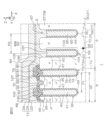
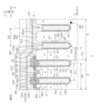
- FIG. 1 is a schematic plan view of a semiconductor device according to an embodiment of the present disclosure
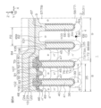
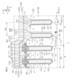
- FIG. FIG. 2 is a plan view schematically showing the structure of the first main surface of the semiconductor device.
- FIG. 3 is an enlarged view of a portion surrounded by a dashed-dotted line III in FIG.
- FIG. 4 is an enlarged view of a portion surrounded by a dashed line IV in FIG. 5 is an enlarged view of a portion surrounded by a dashed line V in FIG. 4.
- FIG. FIG. 6 is an enlarged view of the portion surrounded by the dashed-dotted line VI in FIG. 7 is a cross-sectional view taken along line VII-VII of FIG. 5.
- FIG. 8 is a cross-sectional view taken along line VIII-VIII of FIG. 6.
- FIG. 9 is a cross-sectional view taken along line IX-IX in FIG. 5.
- FIG. 10A is a cross-sectional view of a region corresponding to FIG. 8, and is a cross-sectional view for explaining an example of a method (first basic structure) for manufacturing the semiconductor device of FIG. 1.
- FIG. 10B is a cross-sectional view showing a step after FIG. 10A.
- FIG. 10C is a cross-sectional view showing a step after FIG. 10B.
- FIG. 10D is a cross-sectional view showing a step after FIG. 10C.
- FIG. 10E is a cross-sectional view showing a step after FIG. 10D.
- FIG. 10F is a cross-sectional view showing a step after FIG. 10E.
- FIG. 10A is a cross-sectional view of a region corresponding to FIG. 8, and is a cross-sectional view for explaining an example of a method (first basic structure) for manufacturing the semiconductor device of FIG. 1.
- FIG. 10G is a cross-sectional view showing a step after FIG. 10F.
- FIG. 10H is a cross-sectional view showing a step after FIG. 10G.
- FIG. 10I is a cross-sectional view showing a step after FIG. 10H.
- FIG. 10J is a cross-sectional view showing a step after FIG. 10I.
- FIG. 10K is a cross-sectional view showing a step after FIG. 10J.
- FIG. 10L is a cross-sectional view showing a step after FIG. 10K.
- FIG. 10M is a cross-sectional view showing a step after FIG. 10L.
- FIG. 10N is a cross-sectional view showing a step after FIG. 10M.
- FIG. 10G is a cross-sectional view showing a step after FIG. 10F.
- FIG. 10H is a cross-sectional view showing a step after FIG. 10G.
- FIG. 10I is a cross-sectional view showing
- FIG. 10O is a cross-sectional view showing a step after FIG. 10N.
- FIG. 10P is a cross-sectional view showing a step after FIG. 10O.
- FIG. 10Q is a cross-sectional view showing a step after FIG. 10P.
- FIG. 10R is a cross-sectional view showing a step after FIG. 10Q.
- FIG. 11 is a schematic plan view showing an enlarged part of the second basic structure of the semiconductor device, and is an enlarged view of the part corresponding to FIG.
- FIG. 12 is an enlarged view of the portion surrounded by the dashed-dotted line XII in FIG.
- FIG. 13 is an enlarged view of the portion surrounded by the dashed-dotted line XIII in FIG.
- FIG. 14 is a cross-sectional view taken along line XIV-XIV in FIG. 12.
- FIG. 15 is a cross-sectional view taken along line XV-XV of FIG. 13.
- FIG. 16 is a cross-sectional view taken along line XVI-XVI of FIG. 12.
- FIG. 17A is a cross-sectional view of a region corresponding to FIG. 15, and is a cross-sectional view for explaining an example of the manufacturing method (second basic structure) of the semiconductor device of FIG. 1.
- FIG. FIG. 17B is a cross-sectional view showing a step after FIG. 17A.
- FIG. 17C is a cross-sectional view showing a step after FIG. 17B.
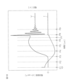
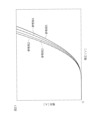
- FIG. 18 is a diagram obtained by examining the reverse recovery characteristics of the pn junction diode of the semiconductor device according to Reference Example 1 by simulation.
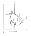
- 19A is a diagram obtained by examining the hole current density of the semiconductor device according to Reference Example 1 by simulation.
- FIG. 19B is a diagram obtained by examining the hole current density of the semiconductor device according to Reference Example 1 by simulation.
- FIG. 19C is a diagram obtained by examining the hole current density of the semiconductor device according to Reference Example 1 by simulation.
- FIG. 19D is a diagram obtained by examining the hole current density of the semiconductor device according to Reference Example 1 by simulation.
- FIG. 19E is a diagram obtained by examining the hole current density of the semiconductor device according to Reference Example 1 by simulation.
- FIG. 19A is a diagram obtained by examining the hole current density of the semiconductor device according to Reference Example 1 by simulation.
- FIG. 19B is a diagram obtained by examining the hole current density of the semiconductor device according to Reference Example 1 by simulation.
- FIG. 19C is a diagram
- FIG. 19F is a diagram obtained by examining the hole current density of the semiconductor device according to Reference Example 1 by simulation.
- FIG. 19G is a diagram obtained by examining the hole current density of the semiconductor device according to Reference Example 1 by simulation.
- FIG. 19H is a diagram obtained by examining the hole current density of the semiconductor device according to Reference Example 1 by simulation.
- FIG. 19I is a diagram obtained by examining the hole current density of the semiconductor device according to Reference Example 1 by simulation.
- 20A is a schematic diagram of a pn junction diode according to Reference Example 2.
- FIG. 20B is a schematic diagram of a pn junction diode according to Reference Example 3.
- FIG. 20C is a schematic diagram of a pn junction diode according to Reference Example 4.
- FIG. 20A is a schematic diagram of a pn junction diode according to Reference Example 2.
- FIG. 20B is a schematic diagram of a pn junction diode according to Reference Example 3.
- FIG. 20C is
- FIG. 20D is a schematic diagram of a pn junction diode according to Reference Example 5.
- FIG. FIG. 21 is a diagram showing the forward characteristics of the pn junction diodes according to Reference Examples 2 to 5 examined by simulation.
- FIG. 22 is a diagram obtained by examining the magnitude of the hole density in the forward direction of the pn junction diodes according to Reference Examples 2 to 5 by simulation.
- FIG. 23 is a diagram showing reverse recovery characteristics of the pn junction diodes according to Reference Examples 2 to 5 examined by simulation.
- FIG. 24 is a schematic cross-sectional view showing the 1-1 improved structure of the semiconductor device.
- FIG. 25 is a schematic cross-sectional view showing the 1-1 improvement structure of the semiconductor device.
- FIG. 26A is a cross-sectional view illustrating the steps involved in forming the structure of FIGS. 24 and 25.
- FIG. FIG. 26B is a cross-sectional view showing a step after FIG. 26A.
- FIG. 26C is a cross-sectional view showing a step after FIG. 26B.
- FIG. 27A is a cross-sectional view illustrating the steps involved in forming the structure of FIGS. 24 and 25;
- FIG. 27B is a cross-sectional view showing a step after FIG. 26A.
- FIG. 28 is a schematic cross-sectional view showing the 1-2 improvement structure of the semiconductor device.
- FIG. 29 is a schematic cross-sectional view showing the 1-2 improvement structure of the semiconductor device.
- FIG. 30A is a cross-sectional view illustrating the steps involved in forming the structure of FIGS. 28 and 29.
- FIG. FIG. 30B is a cross-sectional view showing a step after FIG. 30A.
- FIG. 30C is a cross-sectional view showing a step after FIG. 30B.
- FIG. 31 is a schematic cross-sectional view showing the 1-3 improvement structure of the semiconductor device.
- FIG. 32 is a schematic cross-sectional view showing the 1-3 improved structure of the semiconductor device.
- FIG. 33 is a schematic cross-sectional view showing the 1-4 improvement structure of the semiconductor device.
- FIG. 34 is a schematic cross-sectional view showing the 1-4 improvement structure of the semiconductor device.
- FIG. 35 is a schematic cross-sectional view showing the 2-1 improvement structure of the semiconductor device.
- FIG. 36A is a cross-sectional view illustrating the steps involved in forming the structure of FIG. 35.
- FIG. FIG. 36B is a cross-sectional view showing a step after FIG. 36A.
- FIG. 36C is a cross-sectional view showing a step after FIG. 36B.
- FIG. 36D is a cross-sectional view showing a step after FIG. 36C.
- FIG. 36E is a cross-sectional view showing a step after FIG. 36D.
- FIG. 37 is a schematic cross-sectional view showing the 2-2 improved structure of the semiconductor device.
- FIG. 38 is a schematic cross-sectional view showing the 2-3 improvement structure of the semiconductor device.
- FIG. 39 is a schematic cross-sectional view showing the 2-4 improvement structure of the semiconductor device.
- FIG. 40 is a schematic cross-sectional view showing the 3-1 improved structure of the semiconductor device.
- FIG. 41A is a cross-sectional view illustrating the steps involved in forming the structure of FIG.
- FIG. 41B is a cross-sectional view showing a step after FIG. 41A.
- FIG. 41C is a cross-sectional view showing a step after FIG. 41B.
- FIG. 42 is a schematic cross-sectional view showing the 3-2 improvement structure of the semiconductor device.
- FIG. 43 is a schematic cross-sectional view showing the 4-1 improvement structure of the semiconductor device.
- 44A is a cross-sectional view illustrating the steps involved in forming the structure of FIG. 43.
- FIG. FIG. 44B is a cross-sectional view showing a step after FIG. 44A.
- FIG. 44C is a cross-sectional view showing a step after FIG. 44B.
- FIG. 45 is a schematic cross-sectional view showing the 5-1 improvement structure of the semiconductor device.
- FIG. 46 is a schematic perspective view showing the 5-1 improvement structure of the semiconductor device.
- FIG. 47A is a cross-sectional view illustrating the steps involved in forming the structure of FIG.
- FIG. 47B is a cross-sectional view showing a step after FIG. 47A.
- FIG. 47C is a cross-sectional view showing a step after FIG. 47B.
- FIG. 47D is a cross-sectional view showing a step after FIG. 47C.
- FIG. 47E is a cross-sectional view showing a step after FIG. 47D.
- FIG. 47A is a cross-sectional view illustrating the steps involved in forming the structure of FIG.
- FIG. 47B is a cross-sectional view showing a step after FIG. 47A.
- FIG. 47C is a cross-
- FIG. 48 is a schematic cross-sectional view showing the 6-1 improvement structure of the semiconductor device.
- 49A is a cross-sectional view illustrating the steps involved in forming the structure of FIG. 48.
- FIG. FIG. 49B is a cross-sectional view showing a step after FIG. 49A.
- FIG. 49C is a cross-sectional view showing a step after FIG. 49B.
- FIG. 50 is a schematic cross-sectional view showing the 7-1 improved structure of the semiconductor device.
- FIG. 51 is a cross-sectional view illustrating the steps involved in forming the structure of FIG.
- FIG. 52 is a schematic cross-sectional view showing the 8-1 improvement structure of the semiconductor device.
- FIG. 53 is a schematic cross-sectional view showing the 8-2 improvement structure of the semiconductor device.
- FIG. 54 is a schematic cross-sectional view showing the 8-3 improvement structure of the semiconductor device.
- FIG. 55 is a schematic cross-sectional view showing the 8-4 improved structure of the semiconductor device.
- FIG. 56 is a schematic cross-sectional view showing the 9-1 improvement structure of the semiconductor device.
- FIG. 57 is a schematic cross-sectional view showing the 9-2 improvement structure of the semiconductor device.
- FIG. 58 is a schematic cross-sectional view showing the 9-3 improvement structure of the semiconductor device.
- FIG. 59 is a schematic cross-sectional view showing the 9-4 improvement structure of the semiconductor device.
- FIG. 60 is a schematic cross-sectional view showing the 10-1 improvement structure of the semiconductor device.
- FIG. 61 is a schematic cross-sectional view showing the 10-2 improvement structure of the semiconductor device.
- FIG. 62 is a schematic cross-sectional view showing the 10-3 improvement structure of the semiconductor device.
- FIG. 63 is a schematic cross-sectional view showing the 10-4 improvement structure of the semiconductor device.
- FIG. 64 is a schematic cross-sectional view showing the 11-1 improvement structure of the semiconductor device.
- FIG. 65 is a schematic cross-sectional view showing the 11-2 improvement structure of the semiconductor device.
- FIG. 66 is a schematic cross-sectional view showing the 11-3 improvement structure of the semiconductor device.
- FIG. 67 is a schematic cross-sectional view showing the 11-4 improvement structure of the semiconductor device.
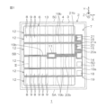
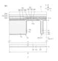
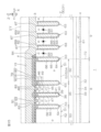
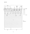
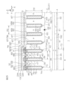
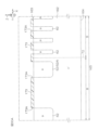
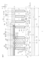
- FIG. 1 is a schematic plan view of a semiconductor device 1 according to an embodiment of the present disclosure.
- FIG. 2 is a plan view schematically showing the structure of the first main surface 3 of the semiconductor device 1.
- FIG. 3 is an enlarged view of a portion surrounded by a dashed-dotted line III in FIG.
- the semiconductor device 1 is an electronic component having an RC-IGBT (Reverse Conducting-Insulated Gate Bipolar Transistor) integrally including an IGBT and a diode.
- RC-IGBT Reverse Conducting-Insulated Gate Bipolar Transistor
- a semiconductor device 1 includes a semiconductor layer 2 having a rectangular parallelepiped shape.
- the semiconductor layer 2 has a first main surface 3 on one side, a second main surface 4 on the other side, and side surfaces 5A, 5B, 5C, 5D connecting the first main surface 3 and the second main surface 4. ing.
- the first main surface 3 and the second main surface 4 are formed in a quadrangular shape when viewed from the normal direction Z (hereinafter simply referred to as "plan view").
- the side surface 5A and the side surface 5C extend along the first direction X and face each other in a second direction Y intersecting the first direction X.
- the side surface 5B and the side surface 5D extend along the second direction Y and face each other in the first direction X.
- the second direction Y is orthogonal to the first direction X.
- the thickness of the semiconductor layer 2 may be from 50 ⁇ m to 200 ⁇ m.
- the thickness of the semiconductor layer 2 may be from 50 ⁇ m to 100 ⁇ m, from 100 ⁇ m to 150 ⁇ m, or from 150 ⁇ m to 200 ⁇ m.
- the semiconductor layer 2 includes an active area 6 and an outer area 7 .
- the active region 6 is a region in which RC-IGBTs are formed.
- the active region 6 is set in the central portion of the semiconductor layer 2 with a space inward from the side surfaces 5A to 5D in plan view.
- the active area 6 may be set in a quadrangular shape having four sides parallel to the side surfaces 5A to 5D in plan view.
- the outer area 7 is an area outside the active area 6 .
- the outer region 7 extends in a strip shape along the periphery of the active region 6 in plan view. Specifically, the outer region 7 is set in an endless shape (square ring shape) surrounding the active region 6 in plan view.
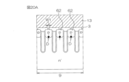
- the active area 6 includes an IGBT area 8 and a diode area 9.
- the diode region 9 is indicated by hatching for clarity.
- the IGBT region 8 is a region in which an IGBT is formed.
- a diode region 9 is a region in which a diode is formed. Diode region 9 is adjacent to IGBT region 8 .
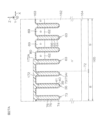
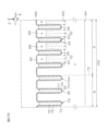
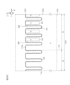
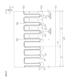
- the active region 6 specifically includes an RC-IGBT array 12.
- a plurality of (six in this embodiment) RC-IGBT arrays 12 are formed at intervals in the second direction Y. As shown in FIG.
- the RC-IGBT array 12 has a first end on one side (side surface 5B) and a second end on the other side (side surface 5D).
- the RC-IGBT array 12 includes an IGBT region 8, a diode region 9, an IGBT region 8, a diode region 9, . It has a loop sequence containing repeats.
- a first end of the RC-IGBT array 12 is formed by an IGBT region 8 in this embodiment.
- the second end of the RC-IGBT array 12 is formed by the IGBT region 8 in this embodiment.
- a first end of the RC-IGBT array 12 may be formed by a diode region 9 .
- a second end of the RC-IGBT array 12 may be formed by a diode region 9 .
- a plurality of IGBT regions 8 are distributed and arranged in the active region 6 .
- the plurality of IGBT regions 8 are spaced apart along the first direction X and the second direction Y. As shown in FIG.
- the plurality of IGBT regions 8 are arranged in a matrix in plan view in this embodiment.
- the plurality of IGBT regions 8 face each other along the first direction X and face each other along the second direction Y. As shown in FIG.
- the plurality of IGBT regions 8 are each formed in a square shape in plan view. Specifically, the plurality of IGBT regions 8 are each formed in a rectangular shape extending along the second direction Y. As shown in FIG.
- width WI of each IGBT region 8 may be 10 ⁇ m or more and 1000 ⁇ m or less.
- the width WI is the width of the IGBT region 8 in the first direction X. As shown in FIG.
- the width WI is 10 ⁇ m or more and 100 ⁇ m or less, 100 ⁇ m or more and 200 ⁇ m or less, 200 ⁇ m or more and 300 ⁇ m or less, 300 ⁇ m or more and 400 ⁇ m or less, 400 ⁇ m or more and 500 ⁇ m or less, 500 ⁇ m or more and 600 ⁇ m or less, 600 ⁇ m or more and 700 ⁇ m or less, 700 ⁇ m or more and 800 ⁇ m or less, 800 ⁇ m or more and 900 ⁇ m or less, or , 900 ⁇ m or more and 1000 ⁇ m or less.
- the width WI is preferably 100 ⁇ m or more. More preferably, the width WI is 200 ⁇ m or more.
- a plurality of diode regions 9 are distributed and arranged in the active region 6 .
- a plurality of diode regions 9 are formed at intervals along the first direction X and the second direction Y. As shown in FIG.
- the plurality of diode regions 9 are arranged in a matrix in plan view in this embodiment.
- the plurality of diode regions 9 face each other along the first direction X and face each other along the second direction Y. As shown in FIG.
- the plurality of diode regions 9 are formed adjacent to the IGBT regions 8 in the first direction X, respectively.
- the plurality of diode regions 9 are each formed in a square shape in plan view in this embodiment.
- the plurality of diode regions 9 are each formed in a rectangular shape extending along the second direction Y. As shown in FIG.
- each diode region 9 is preferably equal to or less than the plane area of each IGBT region 8 . More preferably, the planar area of each diode region 9 is less than the planar area of each IGBT region 8 .
- width WD of each diode region 9 is preferably equal to or less than width WI of each IGBT region 8 .
- the width WD is the width in the first direction X of the diode region 9 . More preferably, the width WD of each diode region 9 is less than the width WI of each IGBT region 8 .
- the width WD may be 5 ⁇ m or more and less than 1000 ⁇ m.
- Width WD is 5 ⁇ m or more, 100 ⁇ m or less, 200 ⁇ m or more, 200 ⁇ m or more, 300 ⁇ m or less, 300 ⁇ m or more, 400 ⁇ m or less, 500 ⁇ m or more, 500 ⁇ m or more, 600 ⁇ m or less, 600 ⁇ m or more, 700 ⁇ m or less, 700 ⁇ m or more.
- the width WD is preferably 100 ⁇ m or more. More preferably, the width WD is 200 ⁇ m or more.
- active area 6 further includes sensor area 11 .
- a sensor area 11 is an area in which a temperature sensor is formed.
- the sensor region 11 is formed in a region between two RC-IGBT arrays 12 adjacent to each other in the second Y direction.
- the sensor area 11 is formed in the central portion of the active area 6 in this embodiment. Heat tends to increase in the central portion of the active region 6 . Therefore, by arranging the temperature sensor in the central portion of the active region 6, the temperature of the semiconductor layer 2 can be detected appropriately.
- the semiconductor device 1 includes an emitter terminal electrode 13 (see dashed line in FIG. 1) as an example of a second electrode formed on the first main surface 3 of the semiconductor layer 2 in the active region 6 .
- Emitter terminal electrode 13 transmits an emitter signal to active region 6 (IGBT region 8).
- the emitter signal may be at reference potential or ground potential.
- the semiconductor device 1 includes a plurality of (five in this embodiment) terminal electrodes 14 , 15 , 16 , 17 , 18 formed on the first main surface 3 of the semiconductor layer 2 in the outer region 7 .
- a plurality of terminal electrodes 14 to 18 are spaced apart from each other along side surface 5D.
- the plurality of terminal electrodes 14 to 18 are formed in a square shape in plan view.
- the multiple terminal electrodes 14 to 18 include the gate terminal electrode 14, the first sense terminal electrode 15, the second sense terminal electrode 16, the current detection terminal electrode 17 and the open terminal electrode 18 in this embodiment.
- Gate terminal electrode 14 transmits a gate signal to active region 6 (IGBT region 8).
- the first sense terminal electrode 15 and the second sense terminal electrode 16 transmit control signals for controlling the sensor region 11 (temperature sensor).
- the current detection terminal electrode 17 is an electrode for detecting a current flowing through the active region 6 and extracting it to the outside.
- the open terminal electrode 18 is in an electrically floating state.
- the arrangement of the gate terminal electrode 14, the first sense terminal electrode 15, the second sense terminal electrode 16, the current detection terminal electrode 17 and the open terminal electrode 18 is arbitrary.
- the open terminal electrode 18, the current detection terminal electrode 17, the gate terminal electrode 14, the first sense terminal electrode 15 and the second sense terminal electrode 16 are arranged in this order from the side surface 5A toward the side surface 5C. ing.
- the semiconductor device 1 includes a gate wiring 19 electrically connected to the gate terminal electrode 14 .
- the gate wiring 19 is also called a gate finger.
- Gate wiring 19 extends from outer region 7 toward active region 6 .
- Gate wiring 19 transmits a gate signal applied to gate terminal electrode 14 to active region 6 (IGBT region 8).
- the gate wiring 19 specifically includes a first region 19 a located in the outer region 7 and a second region 19 b located in the active region 6 .
- the first region 19 a is electrically connected to the gate terminal electrode 14 .
- the first region 19a is selectively routed in the region of the outer region 7 on the side of the side surface 5D.
- a plurality (five in this embodiment) of the second regions 19b are formed in the active region 6 .
- the plurality of second regions 19b are formed along the second direction Y at intervals.
- a plurality of second regions 19b are formed in regions between two RC-IGBT arrays 12 adjacent to each other.
- the multiple second regions 19b extend along the first direction X in a strip shape.
- the plurality of second regions 19b each extend in the outer region 7 from the region on the side surface 5D toward the region on the side surface 5B side.
- a plurality of second regions 19 b may cross the active region 6 .
- the plurality of second regions 19b are connected to the first region 19a in the outer region 7. As shown in FIG.
- the plurality of second regions 19b transmit gate signals to one or both of the two RC-IGBT arrays 12 adjacent to each other.
- a gate signal applied to the gate terminal electrode 14 is transmitted to the second region 19b via the first region 19a. Thereby, the gate signal is transmitted to the active region 6 (IGBT region 8) through the second region 19b.
- the semiconductor device 1 includes first sense wirings 20 electrically connected to first sense terminal electrodes 15 .
- a first sense line 20 extends from the outer region 7 toward the sensor region 11 .
- the first sense wiring 20 transmits a control signal for the temperature sensor.
- the first sense line 20 specifically includes a first region 20 a located in the outer region 7 and a second region 20 b located in the active region 6 .
- the first region 20 a is electrically connected to the first sense terminal electrode 15 .
- the first region 20a is selectively routed in the region of the outer region 7 on the side of the side surface 5D.
- the second region 20b is formed in the region where the sensor region 11 is formed in the region between the multiple RC-IGBT arrays 12 adjacent to each other.
- the second region 20b extends in the first direction X from the outer region 7 toward the sensor region 11 in a strip shape.
- the second area 20b is electrically connected to the temperature sensor in the sensor area 11.
- the second region 20b is connected to the first region 20a in the outer region 7. As shown in FIG. An electric signal applied to the first sense terminal electrode 15 is transmitted to the second region 21b through the first region 20a. Thereby, an electric signal is transmitted to the temperature sensor via the second region 21b.
- a second sense wiring 21 is electrically connected to the second sense terminal electrode 16 .
- a second sense line 21 extends from the outer region 7 toward the sensor region 11 .
- the second sense wiring 21 transmits a control signal for the temperature sensor.
- the second sense line 21 specifically includes a first region 21 a located in the outer region 7 and a second region 21 b located in the active region 6 .
- the first region 21 a is electrically connected to the second sense terminal electrode 16 .
- the first region 21a is selectively routed in the region of the outer region 7 on the side of the side surface 5D.
- the second region 21b is formed in the region where the sensor region 11 is formed in the region between the multiple RC-IGBT arrays 12 adjacent to each other.
- the second region 21b extends in the first direction X from the outer region 7 toward the sensor region 11 in a strip shape.
- the second area 21 b is electrically connected to the temperature sensor in the sensor area 11 .
- the second region 21b is connected to the first region 21a in the outer region 7.
- An electrical signal applied to the second sense terminal electrode 16 is transmitted to the second region 21b through the first region 21a. Thereby, an electric signal is transmitted to the temperature sensor via the second region 21b.
- a gate line 19, a first sense line 20 and a second sense line 21 are formed in a region between a plurality of adjacent RC-IGBT arrays 12 where the sensor region 11 is formed.
- the gate wiring 19, the first sense wiring 20 and the second sense wiring 21 run parallel in the region between the two RC-IGBT arrays 12 adjacent to each other.
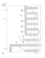
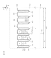
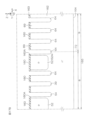
- FIG. 4 is an enlarged view of the portion surrounded by the dashed-dotted line IV in FIG. 5 is an enlarged view of a portion surrounded by a dashed line V in FIG. 4.
- FIG. FIG. 6 is an enlarged view of the portion surrounded by the dashed-dotted line VI in FIG. 7 is a cross-sectional view taken along line VII-VII of FIG. 5.
- FIG. 8 is a cross-sectional view taken along line VIII-VIII of FIG. 6.
- FIG. 9 is a cross-sectional view taken along line IX-IX in FIG. 5.
- FIG. 4 is an enlarged view of the portion surrounded by the dashed-dotted line IV in FIG. 5 is an enlarged view of a portion surrounded by a dashed line V in FIG. 4.
- FIG. 6 is an enlarged view of the portion surrounded by the dashed-dotted line VI in FIG. 7 is a cross-sectional view taken along line VII-VII of FIG. 5.
- FIG. 8 is a cross
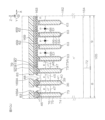
- semiconductor device 1 includes n ⁇ -type drift region 30 formed inside semiconductor layer 2 .
- the drift region 30 is formed over the entire semiconductor layer 2 in the first direction X and the second direction Y. As shown in FIG.
- the drift region 30 is formed in the surface layer portion of the first main surface 3 of the semiconductor layer 2 in the normal direction Z (thickness direction of the semiconductor layer 2).
- the n-type impurity concentration of the drift region 30 may be 1.0 ⁇ 10 13 cm ⁇ 3 or more and 1.0 ⁇ 10 15 cm ⁇ 3 or less.
- the semiconductor layer 2 has a single layer structure including an n ⁇ -type semiconductor substrate 31 in this embodiment.
- the semiconductor substrate 31 may be a silicon FZ substrate formed through the FZ (Floating Zone) method.
- Drift region 30 is formed by a semiconductor substrate 31 .
- the semiconductor device 1 includes a collector terminal electrode 32 as an example of a first electrode formed on the second main surface 4 of the semiconductor layer 2 .
- Collector terminal electrode 32 is electrically connected to second main surface 4 .
- the collector terminal electrode 32 is electrically connected to the IGBT region 8 (collector region 34 described later) and the diode region 9 (cathode region 61 described later).
- the collector terminal electrode 32 forms an ohmic contact with the second principal surface 4 .
- Collector terminal electrode 32 transmits a collector signal to IGBT region 8 and diode region 9 .
- the collector terminal electrode 32 may include at least one of a Ti layer, Ni layer, Au layer, Ag layer and Al layer.
- the collector terminal electrode 32 may have a single layer structure including a Ti layer, Ni layer, Au layer, Ag layer or Al layer.
- the collector terminal electrode 32 may have a laminated structure in which at least two of a Ti layer, a Ni layer, an Au layer, an Ag layer and an Al layer are laminated in any manner.
- the semiconductor device 1 includes an n-type buffer layer 33 formed on the surface layer portion of the second main surface 4 of the semiconductor layer 2 .
- the buffer layer 33 may be formed over the entire surface layer portion of the second main surface 4 .
- the n-type impurity concentration of buffer layer 33 is higher than the n-type impurity concentration of drift region 30 .
- the n-type impurity concentration of the buffer layer 33 may be 1.0 ⁇ 10 15 cm ⁇ 3 or more and 1.0 ⁇ 10 17 cm ⁇ 3 or less.
- the thickness of the buffer layer 33 may be 0.5 ⁇ m or more and 30 ⁇ m or less.
- the thickness of the buffer layer 33 may be 0.5 ⁇ m to 5 ⁇ m, 5 ⁇ m to 10 ⁇ m, 10 ⁇ m to 15 ⁇ m, 15 ⁇ m to 20 ⁇ m, 20 ⁇ m to 25 ⁇ m, or 25 ⁇ m to 30 ⁇ m.
- Each IGBT region 8 includes a p-type collector region 34 formed in the surface layer portion of the second main surface 4 of the semiconductor layer 2 .
- Collector region 34 is exposed from second main surface 4 .
- the collector region 34 may be formed over the entire IGBT region 8 in the surface layer portion of the second main surface 4 .
- the p-type impurity concentration of the collector region 34 may be 1.0 ⁇ 10 15 cm ⁇ 3 or more and 1.0 ⁇ 10 18 cm ⁇ 3 or less.
- Collector region 34 forms an ohmic contact with collector terminal electrode 32 .
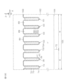
- Each IGBT region 8 includes a FET structure 35 formed on the first main surface 3 of the semiconductor layer 2 .
- Each IGBT region 8 includes a trench gated FET structure 35 in this embodiment.
- FET structure 35 specifically includes a trench gate structure 36 formed in first major surface 3 . 4-6, the trench gate structure 36 is indicated by hatching.
- a plurality of trench gate structures 36 are formed at intervals along the first direction X in the IGBT region 8 .
- a distance between two trench gate structures 36 adjacent to each other in the first direction X may be 1 ⁇ m or more and 8 ⁇ m or less.
- the distance between the two trench gate structures 36 is 1 ⁇ m to 2 ⁇ m, 2 ⁇ m to 3 ⁇ m, 3 ⁇ m to 4 ⁇ m, 4 ⁇ m to 5 ⁇ m, 5 ⁇ m to 6 ⁇ m, 6 ⁇ m to 7 ⁇ m, or 7 ⁇ m to 8 ⁇ m.
- a plurality of trench gate structures 36 are formed in a band shape extending along the second direction Y in plan view.
- a plurality of trench gate structures 36 are formed in a stripe shape as a whole.
- the multiple trench gate structures 36 each have one end on one side in the second direction Y and the other end on the other side in the second direction Y. As shown in FIG.
- FET structure 35 includes first outer trench gate structure 37 and second outer trench gate structure 38 .
- a first outer trench gate structure 37 extends along the first direction X and connects one end of the plurality of trench gate structures 36 .
- a second outer trench gate structure 38 extends along the first direction X and connects other ends of the plurality of trench gate structures 36 .
- the first outer trench gate structure 37 and the second outer trench gate structure 38 have the same structure as the trench gate structure 36 except that they extend in different directions.
- the structure of the trench gate structure 36 will be described below, and the description of the structure of the first outer trench gate structure 37 and the structure of the second outer trench gate structure 38 will be omitted.
- Each trench gate structure 36 includes a gate trench 39 , a gate insulating layer 40 and a gate electrode layer 41 .
- Gate trench 39 is formed in first main surface 3 .
- Gate trench 39 includes sidewalls and a bottom wall. A sidewall of gate trench 39 may be formed perpendicular to first main surface 3 .
- the side walls of the gate trench 39 may slope downward from the first main surface 3 toward the bottom wall.
- Gate trench 39 may be formed in a tapered shape in which the opening area on the opening side is larger than the bottom area.
- a bottom wall of gate trench 39 may be formed parallel to first main surface 3 .
- the bottom wall of gate trench 39 may be curved toward second main surface 4 .
- Gate trench 39 includes a bottom wall edge. The bottom wall edge portion connects the side wall and the bottom wall of gate trench 39 .
- the bottom wall edge portion may be curved toward the second main surface 4 .
- the depth D1 of the gate trench 39 may be 2 ⁇ m or more and 10 ⁇ m or less.
- the depth D1 of the gate trench 39 may be 2 ⁇ m or more and 3 ⁇ m or less, 3 ⁇ m or more and 4 ⁇ m or less, 4 ⁇ m or more and 5 ⁇ m or less, 5 ⁇ m or more and 6 ⁇ m or less, 6 ⁇ m or more and 7 ⁇ m or less, 8 ⁇ m or more and 9 ⁇ m or less, or 9 ⁇ m or more and 10 ⁇ m or less.
- Depth D1 of gate trench 39 may be defined as the distance between the deepest portion of the bottom wall of gate trench 39 and first main surface 3 .
- the width of the gate trench 39 may be 0.5 ⁇ m or more and 3 ⁇ m or less.
- the width of the gate trench 39 is the width in the first direction X of the gate trench 39 .
- the width of the gate trench 39 may be 0.5 ⁇ m to 1 ⁇ m, 1 ⁇ m to 1.5 ⁇ m, 1.5 ⁇ m to 2 ⁇ m, 2 ⁇ m to 2.5 ⁇ m, or 2.5 ⁇ m to 3 ⁇ m.
- the gate insulating layer 40 is formed like a film along the inner wall of the gate trench 39 .
- the gate insulating layer 40 defines a recess space within the gate trench 39 .
- Gate insulating layer 40 includes a silicon oxide film in this embodiment.
- the gate insulating layer 40 may contain a silicon nitride film instead of or in addition to the silicon oxide film.
- the gate electrode layer 41 is embedded in the gate trench 39 with the gate insulating layer 40 interposed therebetween. Specifically, the gate electrode layer 41 is embedded in a recess space partitioned by the gate insulating layer 40 in the gate trench 39 . The gate electrode layer 41 is controlled by a gate signal. Gate electrode layer 41 may include conductive polysilicon.
- the gate electrode layer 41 is formed in a wall shape extending along the normal direction Z when viewed in cross section. Gate electrode layer 41 has an upper end located on the opening side of gate trench 39 . The upper end of gate electrode layer 41 is located on the bottom wall side of gate trench 39 with respect to first main surface 3 .
- a recess that is recessed toward the bottom wall of the gate trench 39 is formed in the upper end of the gate electrode layer 41 .
- the depression at the upper end of gate electrode layer 41 is tapered toward the bottom wall of gate trench 39 .
- the upper end portion of the gate electrode layer 41 has a constricted portion constricted inside the gate electrode layer 41 .
- the FET structure 35 includes a p-type body region 45 formed in the surface layer portion of the first main surface 3 of the semiconductor layer 2 .
- the p-type impurity concentration of body region 45 may be 1.0 ⁇ 10 17 cm ⁇ 3 or more and 1.0 ⁇ 10 18 cm ⁇ 3 or less.
- a body region 45 is formed on each side of the trench gate structure 36 .
- Body region 45 is formed in a strip shape extending along trench gate structure 36 in plan view. Body region 45 is exposed from the sidewall of gate trench 39 .
- the bottom of body region 45 is formed in a region between first main surface 3 and the bottom wall of gate trench 39 with respect to normal direction Z. As shown in FIG.
- the FET structure 35 includes an n + -type emitter region 46 formed in the surface layer of the body region 45 .
- the n-type impurity concentration of emitter region 46 is higher than the n-type impurity concentration of drift region 30 .
- the n-type impurity concentration of the emitter region 46 may be 1.0 ⁇ 10 19 cm ⁇ 3 or more and 1.0 ⁇ 10 20 cm ⁇ 3 or less.
- FET structure 35 includes a plurality of emitter regions 46 formed on opposite sides of trench gate structure 36 in this embodiment.
- the emitter region 46 is formed in a strip shape extending along the trench gate structure 36 in plan view. Emitter region 46 is exposed from first main surface 3 and sidewalls of gate trench 39 .
- the bottom of emitter region 46 is formed in a region between the upper end of gate electrode layer 41 and the bottom of body region 45 with respect to normal direction Z. As shown in FIG.
- the FET structure 35 includes, in this embodiment, an n + -type carrier storage region 47 formed in a region on the second main surface 4 side with respect to the body region 45 in the semiconductor layer 2 .
- the n-type impurity concentration of carrier storage region 47 is higher than the n-type impurity concentration of drift region 30 .
- the n-type impurity concentration of the carrier storage region 47 may be 1.0 ⁇ 10 15 cm ⁇ 3 or more and 1.0 ⁇ 10 17 cm ⁇ 3 or less.
- the FET structure 35 includes a plurality of carrier storage regions 47 formed on either side of the trench gate structure 36 in this embodiment.
- the carrier storage region 47 is formed in a strip shape extending along the trench gate structure 36 in plan view. Carrier storage region 47 is exposed from the sidewalls of gate trench 39 .
- the bottom of carrier storage region 47 is formed in the region between the bottom of body region 45 and the bottom wall of gate trench 39 with respect to normal direction Z.
- the carrier storage region 47 suppresses the carriers (holes) supplied to the semiconductor layer 2 from being drawn back (ejected) to the body region 45 . As a result, holes are accumulated in the semiconductor layer 2 in the region immediately below the FET structure 35 . As a result, it is possible to reduce the on-resistance and the on-voltage.
- the FET structure 35 includes contact trenches 48 formed in the first main surface 3 of the semiconductor layer 2 .
- FET structure 35 includes a plurality of contact trenches 48 formed on opposite sides of trench gate structure 36 in this embodiment.
- a contact trench 48 exposes the emitter region 46 .
- Contact trench 48 extends through emitter region 46 in this embodiment.
- the contact trench 48 is formed spaced apart in the first direction X from the trench gate structure 36 .
- the contact trench 48 extends in a strip shape along the trench gate structure 36 in plan view. With respect to the second direction Y, the length of contact trench 48 is less than or equal to the length of trench gate structure 36 .
- the length of contact trench 48 is specifically less than the length of trench gate structure 36 .
- FET structure 35 includes a p + type contact region 49 formed in a region along the bottom wall of contact trench 48 in body region 45 .
- the p-type impurity concentration of contact region 49 is higher than the p-type impurity concentration of body region 45 .
- the p-type impurity concentration of the contact region 49 may be 1.0 ⁇ 10 19 cm ⁇ 3 or more and 1.0 ⁇ 10 20 cm ⁇ 3 or less.
- the contact region 49 is exposed from the bottom wall of the contact trench 48 .
- the contact region 49 extends in a strip shape along the contact trench 48 in plan view.
- the bottom of the contact region 49 is formed in the region between the bottom wall of the contact trench 48 and the bottom of the body region 45 with respect to the normal direction Z. As shown in FIG.
- the gate electrode layer 41 faces the body region 45 and the emitter region 46 with the gate insulating layer 40 interposed therebetween.
- the gate electrode layer 41 also faces the carrier storage region 47 with the gate insulating layer 40 interposed therebetween.
- the channel of the IGBT is formed in the body region 45 in the region between the emitter region 46 and the drift region 30 (carrier storage region 47). Channel on/off is controlled by a gate signal.
- Each IGBT region 8 includes an emitter trench structure 73 on the first main surface 3 of the semiconductor layer 2 .
- Each IGBT region 8 specifically includes a plurality of emitter trench structures 73 formed on opposite sides of FET structure 35 .
- the emitter trench structure 73 is formed in a region adjacent to the FET structure 35 in the surface layer portion of the first main surface 3 .
- the emitter trench structure 73 is formed in a band shape extending along the second direction Y in plan view.
- a plurality of emitter trench structures 73 are formed in a stripe shape as a whole.
- the emitter trench structure 73 may be strip-shaped parallel to the trench gate structure 36 .
- the trench gate structures 36 and the emitter trench structures 73 are alternately arranged along the first direction X at intervals. These trench structures formed in the IGBT region 8 may be collectively referred to as a second trench structure. Trench gate structures 36 and emitter trench structures 73 may be equally spaced and staggered. A distance (first pitch P1) between two trench gate structures 36 and emitter trench structures 73 adjacent to each other in the first direction X may be, for example, 1.0 ⁇ m or more and 3.5 ⁇ m or less.
- the terminating trenches of the trench gate structures 36 and the emitter trench structures 73 alternately arranged along the first direction X are the emitter trench structures 73 .
- This terminal emitter trench structure 73 (shown as emitter trench structure 73A in FIGS. 4, 6 and 8) forms a boundary 72 between the IGBT region 8 and the diode region 9. As shown in FIG.
- the emitter trench structure 73 includes an emitter trench 74 , an emitter insulating layer 75 and an emitter potential electrode layer 76 .
- Emitter trench 74 is formed in first main surface 3 of semiconductor layer 2 .
- Emitter trench 74 includes sidewalls and a bottom wall. A sidewall of emitter trench 74 may be formed perpendicular to first main surface 3 .
- the side walls of the emitter trench 74 may slope downward from the first main surface 3 toward the bottom wall.
- the emitter trench 74 may be tapered such that the opening area on the opening side is larger than the bottom area.
- Emitter region 46 , body region 45 and carrier storage region 47 are exposed from sidewalls (outer sidewalls) of emitter trench 74 facing FET structure 35 .
- a bottom wall of emitter trench 74 may be formed parallel to first main surface 3 .
- the bottom wall of emitter trench 74 may be curved toward second main surface 4 .
- Emitter trench 74 includes a bottom wall edge.
- the bottom wall edge connects the side and bottom walls of emitter trench 74 .
- the bottom wall edge portion may be curved toward the second main surface 4 of the semiconductor layer 2 .
- the depth D3 of the emitter trench 74 may be 2 ⁇ m or more and 10 ⁇ m or less.
- the depth D3 of the emitter trench 74 may be 2 ⁇ m or more and 3 ⁇ m or less, 3 ⁇ m or more and 4 ⁇ m or less, 4 ⁇ m or more and 5 ⁇ m or less, 5 ⁇ m or more and 6 ⁇ m or less, 6 ⁇ m or more and 7 ⁇ m or less, 8 ⁇ m or more and 9 ⁇ m or less, or 9 ⁇ m or more and 10 ⁇ m or less.
- Depth D3 of emitter trench 74 may be equal to depth D2 of gate trench 39 .
- the width of the emitter trench 74 may be 0.5 ⁇ m or more and 3 ⁇ m or less.
- the width of the emitter trench 74 is the width in the first direction X of the emitter trench 74 .
- the width of the emitter trench 74 may be 0.5 ⁇ m to 1 ⁇ m, 1 ⁇ m to 1.5 ⁇ m, 1.5 ⁇ m to 2 ⁇ m, 2 ⁇ m to 2.5 ⁇ m, or 2.5 ⁇ m to 3 ⁇ m.
- the width of emitter trench 74 may be equal to the width of gate trench 39 .
- the emitter insulating layer 75 is formed like a film along the inner wall of the emitter trench 74 .
- the emitter insulating layer 75 defines a recessed space within the emitter trench 74 .
- Emitter insulating layer 75 includes a silicon oxide film in this embodiment.
- Emitter insulating layer 75 may include a silicon nitride film instead of or in addition to the silicon oxide film.
- the emitter potential electrode layer 76 is embedded in the emitter trench 74 with the emitter insulating layer 75 interposed therebetween. Specifically, the emitter potential electrode layer 76 is embedded in a recess space partitioned by the emitter insulating layer 75 in the emitter trench 74 . Emitter potential electrode layer 76 may include conductive polysilicon. Emitter potential electrode layer 76 is controlled by an emitter signal.
- the emitter potential electrode layer 76 is formed like a wall extending along the normal direction Z when viewed in cross section. Emitter potential electrode layer 76 has an upper end located on the opening side of emitter trench 74 . The upper end of emitter potential electrode layer 76 is located on the bottom wall side of emitter trench 74 with respect to first main surface 3 .
- a recess that is recessed toward the bottom wall of the emitter trench 74 is formed in the upper end portion of the emitter potential electrode layer 76 .
- the recess at the upper end of emitter potential electrode layer 76 is tapered toward the bottom wall of emitter trench 74 .
- the upper end portion of the emitter potential electrode layer 76 has a constricted portion constricted inside the emitter potential electrode layer 76 .
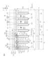
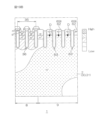
- Each diode region 9 includes an n + -type cathode region 61 (second impurity region) formed in the surface layer portion of the second main surface 4 of the semiconductor layer 2 .
- the n-type impurity concentration of cathode region 61 is higher than the n-type impurity concentration of drift region 30 .
- the n-type impurity concentration of cathode region 61 may be 1.0 ⁇ 10 19 cm ⁇ 3 or more and 1.0 ⁇ 10 20 cm ⁇ 3 or less.
- the cathode region 61 is exposed from the second main surface 4 .
- Cathode region 61 forms an ohmic contact with collector terminal electrode 32 .
- the cathode region 61 is electrically connected to the collector region 34 along the second direction Y side.
- Cathode region 61 is surrounded by collector region 34 of IGBT region 8 in this embodiment. That is, the cathode region 61 is electrically connected to the collector region 34 along the first direction X side and the second direction Y side.
- Each diode region 9 includes a cell separation structure 63 that partitions diode cell regions 69 . 4 and 6, the cell isolation structure 63 is indicated by hatching. Each diode region 9 specifically includes a plurality of cell isolation structures 63 that partition a plurality of diode cell regions 69 respectively.
- a plurality of cell isolation structures 63 are formed in regions between a plurality of diode cell regions 69 adjacent to each other. Specifically, each of the plurality of cell isolation structures 63 is formed in an annular shape (in this embodiment, a square annular shape) surrounding the diode cell region 69 in plan view.
- the cell isolation structure 63 that partitions one diode cell region 69 and the cell isolation structure 63 that partitions the other diode cell region 69 are integrally formed in the region between the plurality of diode cell regions 69 adjacent to each other. .
- the plurality of cell separation structures 63 may be arranged at equal intervals in the first direction X.
- a plurality of cell isolation structures 63 are formed in stripes.
- a distance (second pitch P2) between two cell isolation structures 63 adjacent to each other in first direction X may be, for example, 1.0 ⁇ m or more and 10.0 ⁇ m or less.
- the second pitch P2 may be the same as the first pitch P1 (see FIG. 5).
- a plurality of diode cell regions 69 partitioned by a plurality of cell isolation structures 63 are formed at intervals along the first direction X in plan view.
- the plurality of diode cell regions 69 are each formed in a strip shape extending along the second direction Y in plan view.
- a plurality of diode cell regions 69 are formed in a stripe shape as a whole.
- the diode cell region 69 partially overlaps the collector region 34 and the remainder overlaps the cathode region 61 in the normal direction Z in this embodiment.
- the length of the diode cell region 69 may be less than or equal to the length of the trench gate structure 36 .
- the length of diode cell region 69 may be less than the length of trench gate structure 36 .
- the cell isolation structure 63 includes a cell isolation trench 64 as an example of a first trench, a cell isolation insulating layer 65 as an example of a first insulating layer, and a cell isolation electrode layer 66 as an example of a first embedded conductive layer.
- Cell isolation trenches 64 are formed in first main surface 3 .
- Cell isolation trenches 64 include sidewalls and bottom walls. A sidewall of cell isolation trench 64 may be formed perpendicular to first main surface 3 .
- the side wall of the cell isolation trench 64 may slope downward from the first main surface 3 toward the bottom wall.
- the cell isolation trench 64 may be formed in a tapered shape in which the opening area on the opening side is larger than the bottom area.
- a bottom wall of the cell isolation trench 64 may be formed parallel to the first main surface 3 .
- a bottom wall of the cell isolation trench 64 may be curved toward the second main surface 4 .
- Cell isolation trenches 64 include bottom wall edges. The bottom wall edge portion connects the side wall and bottom wall of the cell isolation trench 64 . The bottom wall edge portion may be curved toward the second main surface 4 .
- the depth D2 of the cell isolation trench 64 may be 2 ⁇ m or more and 10 ⁇ m or less.
- the depth D2 of the cell isolation trench 64 may be 2 ⁇ m or more and 3 ⁇ m or less, 3 ⁇ m or more and 4 ⁇ m or less, 4 ⁇ m or more and 5 ⁇ m or less, 5 ⁇ m or more and 6 ⁇ m or less, 6 ⁇ m or more and 7 ⁇ m or less, 8 ⁇ m or more and 9 ⁇ m or less, or 9 ⁇ m or more and 10 ⁇ m or less. good.
- the depth D2 of the cell isolation trench 64 may be equal to the depth D1 of the gate trench 39 (see FIG. 7).
- the depth D2 of the cell isolation trench 64 may be defined as the distance between the deepest portion of the bottom wall of the cell isolation trench 64 and the first main surface 3 .
- the width of the cell isolation trench 64 may be 0.5 ⁇ m or more and 3 ⁇ m or less.
- the width of the cell isolation trench 64 is the width in the first direction X of the cell isolation trench 64 .
- the width of the cell isolation trench 64 may be 0.5 ⁇ m to 1 ⁇ m, 1 ⁇ m to 1.5 ⁇ m, 1.5 ⁇ m to 2 ⁇ m, 2 ⁇ m to 2.5 ⁇ m, or 2.5 ⁇ m to 3 ⁇ m.
- the width of the cell isolation trenches 64 may be equal to the width of the gate trenches 39 .
- the cell isolation insulating layer 65 is formed like a film along the inner wall of the cell isolation trench 64 .
- the cell isolation insulating layer 65 defines a recess space within the cell isolation trench 64 .
- the cell isolation insulating layer 65 includes a silicon oxide film in this embodiment.
- Cell isolation insulating layer 65 may include a silicon nitride film instead of or in addition to the silicon oxide film.
- the cell isolation electrode layer 66 is embedded in the cell isolation trench 64 with the cell isolation insulating layer 65 interposed therebetween. Specifically, the cell isolation electrode layer 66 is embedded in a recess space partitioned by the cell isolation insulating layer 65 in the cell isolation trench 64 . Cell isolation electrode layer 66 is controlled by an emitter signal. Cell isolation electrode layer 66 may include conductive polysilicon.
- the cell separation electrode layer 66 is formed in a wall shape extending along the normal direction Z when viewed in cross section.
- the cell isolation electrode layer 66 has an upper end located on the opening side of the cell isolation trench 64 .
- the upper end of the cell isolation electrode layer 66 is located on the bottom wall side of the cell isolation trench 64 with respect to the first main surface 3 .
- the upper end portion of the cell separation electrode layer 66 is tapered toward the first main surface 3 side.
- a recess that is recessed toward the bottom wall of the cell isolation trench 64 is formed in the upper end portion of the cell isolation electrode layer 66 .
- the depression of the cell isolation electrode layer 66 is tapered toward the bottom wall of the cell isolation trench 64 .
- Each diode region 9 includes a p ⁇ -type anode region 62 (second impurity region) formed in the surface layer portion of the first main surface 3 of the semiconductor layer 2 .
- the p-type impurity concentration of the anode region 62 may be equal to or less than the p-type impurity concentration of the body region 45 .
- the p-type impurity concentration of anode region 62 is preferably less than the p-type impurity concentration of body region 45 .
- the p-type impurity concentration of the anode region 62 may be 1.0 ⁇ 10 15 cm ⁇ 3 or more and less than 1.0 ⁇ 10 18 cm ⁇ 3 .
- the anode region 62 is formed in each diode cell region 69 . Therefore, the plurality of anode regions 62 are arranged at equal intervals in the first direction X, and are formed in a stripe shape as a whole.
- the anode region 62 forms a pn junction 68 with the semiconductor layer 2 .
- a pn junction diode D having the anode region 62 as an anode and the semiconductor layer 2 (cathode region 61) as a cathode is formed.
- collector region 34 includes lead region 182 in this embodiment.
- the lead-out region 182 is led out to the periphery of the diode region 9 across the boundary 72 between the IGBT region 8 and the diode region 9 .
- the extraction region 182 is extracted along the first direction X from the IGBT region 8 to the diode region 9 .
- the lead region 182 overlaps the diode region 9 with a predetermined overlap width W.
- a starting point of the overlap width W is set at a boundary 72 between the IGBT region 8 and the diode region 9 .
- the end point of the overlap width W is set at the boundary between the extraction region 182 and the cathode region 61 .
- the ratio W/WD of the overlapping width W to the width WD of the diode region 9 may be 0.001 or more and 0.5 or less.
- the ratio W/WD is 0.001 or more and 0.01 or less, 0.01 or more and 0.05 or less, 0.05 or more and 0.1 or less, 0.1 or more and 0.15 or less, 0.15 or more and 0.2 or less. , 0.2 to 0.25, 0.25 to 0.3, 0.3 to 0.35, 0.35 to 0.4, 0.4 to 0.45, or 0.25 to 0.35. It may be 45 or more and 0.5 or less.
- the overlapping width W may be 1 ⁇ m or more and 200 ⁇ m or less.
- the overlapping width W may be 1 ⁇ m or more and 50 ⁇ m or less, 50 ⁇ m or more and 100 ⁇ m or less, 100 ⁇ m or more and 150 ⁇ m or less, or 150 ⁇ m or more and 200 ⁇ m or less.
- the overlapping width W is 1 ⁇ m or more and 20 ⁇ m or less, 20 ⁇ m or more and 40 ⁇ m or less, 40 ⁇ m or more and 60 ⁇ m or less, 60 ⁇ m or more and 80 ⁇ m or less, 80 ⁇ m or more and 100 ⁇ m or less, 100 ⁇ m or more and 120 ⁇ m or less, 120 ⁇ m or more and 140 ⁇ m or less, 140 ⁇ m or more and 160 ⁇ m or less, 160 ⁇ m or more and 180 ⁇ m or less, Alternatively, it may be 180 ⁇ m or more and 200 ⁇ m or less.
- the overlapping width W is preferably 10 ⁇ m or more and 150 ⁇ m or less.
- the extraction region 182 may face one or more anode regions 62 (diode cell regions 69) with respect to the normal direction Z.
- the drawer areas 182 are 1, 2, 3, 4, 5, 6, 7, 8, 9, 10, 11, 12, 13, 14, 15, There may be 16, 17, 18, 19 or 20 anode regions 62 facing each other. It is preferable that the lead region 182 faces one to ten anode regions 62 .
- the lead region 182 may face one or a plurality of cell isolation trenches 64 with respect to the normal direction Z.
- the drawer areas 182 are 1, 2, 3, 4, 5, 6, 7, 8, 9, 10, 11, 12, 13, 14, 15, It may face 16, 17, 18, 19 or 20 cell isolation trenches 64 .
- the lead region 182 preferably faces one to ten cell isolation trenches 64 .
- a recess 67 is defined in the cell isolation trench 64 by the side wall of the cell isolation trench 64 , the upper end of the cell isolation electrode layer 66 and the upper end of the cell isolation insulating layer 65 .
- a wide portion of the cell isolation trench 64 is formed by a recess 67 .
- Side walls of the recess 67 (side walls of the cell isolation trenches 64) expose the anode region 62. As shown in FIG.
- the structure closest to the diode region 9 among the plurality of emitter trench structures 73 is the terminating emitter trench structure 73A.
- the sidewalls of the terminating emitter trench structure 73A on the side closer to the diode region 9 form a boundary 72 between the IGBT region 8 and the diode region 9.
- FIG. 1 In the region between the terminating emitter trench structure 73A and the cell isolation structure 63 closest to the IGBT region 8, similarly to the FET structure 35, the body region 45 and the carrier storage region 47 are formed in order from the first main surface 3 side.
- this region may be referred to as a dummy FET structure 42, since the emitter region 46 is not formed in this region and the structure does not form a channel.
- a dummy FET structure 42 is formed in the diode region 9 .
- semiconductor device 1 includes an interlayer insulating layer 79 formed on first main surface 3 of semiconductor layer 2 .
- the interlayer insulating layer 79 is formed in a film shape along the first main surface 3 and selectively covers the first main surface 3 .
- the interlayer insulating layer 79 specifically covers the IGBT region 8 and the diode region 9 selectively.
- the interlayer insulating layer 79 may contain silicon oxide or silicon nitride. Interlayer insulating layer 79 may contain at least one of NSG (Non-doped Silicate Glass), PSG (Phosphor Silicate Glass) and BPSG (Boron Phosphor Silicate Glass).
- NSG Non-doped Silicate Glass
- PSG Phosphor Silicate Glass
- BPSG Boron Phosphor Silicate Glass
- the thickness of the interlayer insulating layer 79 may be 0.1 ⁇ m or more and 1 ⁇ m or less.
- the thickness of the interlayer insulating layer 79 is 0.1 ⁇ m to 0.2 ⁇ m, 0.2 ⁇ m to 0.4 ⁇ m, 0.4 ⁇ m to 0.6 ⁇ m, 0.6 ⁇ m to 0.8 ⁇ m, or 0.8 ⁇ m. It may be greater than or equal to 1 ⁇ m or less.
- the interlayer insulating layer 79 in this embodiment has a laminated structure including a first insulating layer 80, a second insulating layer 81 and a third insulating layer 82 laminated in this order from the first main surface 3 side.
- the first insulating layer 80 preferably contains silicon oxide (for example, a thermal oxide film).
- the second insulating layer 81 preferably includes an NGS layer.
- the second insulating layer 81 may include a PSG layer or a BPSG layer instead of the NGS layer.
- the third insulating layer 82 preferably includes a BPSG layer.
- the third insulating layer 82 may include an NGS layer or a PSG layer instead of the BPSG layer.
- the third insulating layer 82 preferably contains an insulating material having properties different from those of the second insulating layer 81 .
- the first insulating layer 80 is formed in the form of a film on the first main surface 3 .
- the first insulating layer 80 continues to the gate insulating layer 40 , the region isolation insulating layer 55 and the cell isolation insulating layer 65 .
- the second insulating layer 81 is formed in a film shape on the first insulating layer 80 .
- the third insulating layer 82 is formed in a film shape on the second insulating layer 81 .
- the thickness of the first insulating layer 80 may be 500 ⁇ or more and 2000 ⁇ or less.
- the thickness of the first insulating layer 80 may be 500 ⁇ to 1000 ⁇ , 1000 ⁇ to 1500 ⁇ , or 1500 ⁇ to 2000 ⁇ .
- the thickness of the second insulating layer 81 may be 500 ⁇ or more and 4000 ⁇ or less.
- the thickness of the second insulating layer 81 is 500 ⁇ to 1000 ⁇ , 1000 ⁇ to 1500 ⁇ , 1500 ⁇ to 2000 ⁇ , 2000 ⁇ to 2500 ⁇ , 2500 ⁇ to 3000 ⁇ , 3000 ⁇ to 3500 ⁇ , or 3500 ⁇ to 4000 ⁇ . good.
- the thickness of the third insulating layer 82 may be 1000 ⁇ or more and 8000 ⁇ or less.
- the thickness of the third insulating layer 82 may be 1000 ⁇ to 2000 ⁇ , 2000 ⁇ to 4000 ⁇ , 4000 ⁇ to 6000 ⁇ , or 6000 ⁇ to 8000 ⁇ .
- the gate electrode layer 41 of the FET structure 35 has a gate lead-out electrode layer 41 a drawn out from the gate trench 39 onto the first main surface 3 .
- the gate lead-out electrode layer 41 a is led out onto the first main surface 3 from the gate trench 39 of the first outer trench gate structure 37 .
- the gate extraction electrode layer 41a is extracted along the second direction Y. As shown in FIG.
- the gate lead-out electrode layer 41 a is formed inside the interlayer insulating layer 79 .
- the gate lead-out electrode layer 41 a is led out onto the first insulating layer 80 and interposed in the region between the first insulating layer 80 and the second insulating layer 81 .
- Gate extraction electrode layer 41a is electrically connected to gate wiring 19 (see FIG. 1) in a region not shown.
- a gate signal applied to gate terminal electrode 14 is transmitted to gate electrode layer 41 via gate interconnection 19 and gate lead-out electrode layer 41a.
- emitter potential electrode layer 76 of emitter trench structure 73 has lead electrode layer 76 a led out from emitter trench 74 onto first main surface 3 .
- the emitter potential electrode layer 76 is drawn out along the second direction Y. As shown in FIG.
- the extraction electrode layer 76 a is formed inside the interlayer insulating layer 79 .
- the extraction electrode layer 76 a is extracted onto the first insulating layer 80 and interposed in the region between the first insulating layer 80 and the second insulating layer 81 .
- the extraction electrode layer 76 a is electrically connected to the emitter terminal electrode 13 .
- the emitter signal applied to lead electrode layer 76a is transmitted to emitter potential electrode layer 76 via lead electrode layer 76a.
- interlayer insulating layer 79 includes emitter opening 83.
- FIG. Emitter opening 83 exposes contact trench 48 .
- Emitter opening 83 communicates with contact trench 48 .
- the contact trenches 48 are formed in the first main surface 3 through the first insulating layer 80 and the second insulating layer 81 in this embodiment.
- the emitter opening 83 penetrates the third insulating layer 82 and exposes the contact trench 48 .
- Emitter opening 83 forms one opening with contact trench 48 .
- An opening edge portion of the emitter opening 83 is curved inwardly of the interlayer insulating layer 79 . Thereby, the emitter opening 83 has an opening width larger than that of the contact trench 48 .
- interlayer insulating layer 79 includes diode opening 84 .
- Diode opening 84 exposes diode region 9 .
- the diode openings 84 penetrate the interlayer insulating layer 79 to expose the plurality of anode regions 62 (diode cell regions 69) and the plurality of cell isolation structures 63. As shown in FIG.
- a portion of the inner wall of the diode opening 84 along the second direction Y may be positioned above the anode region 62 .
- a portion of the inner wall of the diode opening 84 along the second direction Y may be positioned above the cell isolation structure 63 .
- a portion of the inner wall of the diode opening 84 along the second direction Y is located on the body region 45 of the dummy FET structure 42 in this embodiment.
- interlayer insulating layer 79 includes first opening 86 .
- the first opening 86 exposes the extraction electrode layer 76 a in the IGBT region 8 .
- the first opening 86 is formed so that the opening width narrows from the opening side toward the bottom wall side.
- semiconductor device 1 includes an emitter plug electrode 91 embedded in a portion of interlayer insulating layer 79 covering IGBT region 8 .
- Emitter plug electrode 91 penetrates interlayer insulating layer 79 and is electrically connected to emitter region 46 and contact region 49 .
- the emitter plug electrode 91 is embedded in the contact trench 48 .
- Emitter plug electrode 91 is electrically connected to emitter region 46 and contact region 49 within contact trench 48 .
- the emitter plug electrode 91 has a laminated structure including a barrier electrode layer 92 and a main electrode layer 93 in this embodiment.
- the barrier electrode layer 92 is formed in a film shape along the inner wall of the contact trench 48 so as to be in contact with the interlayer insulating layer 79 .
- the barrier electrode layer 92 defines recess spaces in the contact trenches 48 .
- the barrier electrode layer 92 may have a single layer structure including a titanium layer or a titanium nitride layer.
- Barrier electrode layer 92 may have a laminated structure including a titanium layer and a titanium nitride layer. In this case, the titanium nitride layer may be laminated on the titanium layer.
- the main electrode layer 93 is embedded in the contact trench 48 with the barrier electrode layer 92 interposed therebetween. Specifically, the main electrode layer 93 is embedded in a recess space partitioned by the barrier electrode layer 92 in the contact trench 48 .
- the main electrode layer 93 may contain tungsten.
- semiconductor device 1 includes a first plug electrode 94 embedded in first opening 86 .
- the first plug electrode 94 is electrically connected to the extraction electrode layer 76a inside the first opening 86 .
- the first plug electrode 94 has a structure corresponding to the emitter plug electrode 91 .
- the description of the emitter plug electrode 91 applies mutatis mutandis to the description of the first plug electrode 94 .
- the structures of the first plug electrode 94 corresponding to the structure described for the emitter plug electrode 91 are denoted by the same reference numerals, and the description thereof is omitted.
- Emitter terminal electrode 13 is formed on an interlayer insulating layer 79. As shown in FIG. Emitter terminal electrode 13 may contain at least one of aluminum, copper, aluminum-silicon-copper alloy, aluminum-silicon alloy, and aluminum-copper alloy.
- the emitter terminal electrode 13 may have a single layer structure containing any one of these conductive materials.
- Emitter terminal electrode 13 may have a laminated structure in which at least two of these conductive materials are laminated in an arbitrary order.
- the thickness of the emitter terminal electrode 13 may be 1.0 ⁇ m or more and 6.0 ⁇ m or less.
- the thickness of the emitter terminal electrode 13 may be 1.0 ⁇ m or more and 2.0 ⁇ m or less, 2.0 ⁇ m or more and 4.0 ⁇ m or less, or 4.0 ⁇ m or more and 6.0 ⁇ m or less.
- the emitter terminal electrode 13 in this embodiment has a laminated structure including a first electrode layer 22, a second electrode layer 23 and a third electrode layer 24 laminated in this order from the first main surface 3 side.
- the first electrode layer 22 preferably contains an aluminum-silicon-copper alloy (Al-Si-Cu).
- the second electrode layer 23 preferably contains titanium nitride (TiN).
- the second electrode layer 23 may be called a barrier layer.
- the third electrode layer 24 preferably contains an aluminum-copper alloy (Al--Cu).
- the emitter terminal electrode 13 is electrically connected to the emitter region 46 and the contact region 49 via the emitter plug electrode 91 on the interlayer insulating layer 79 . Specifically, the emitter terminal electrode 13 enters the emitter opening 83 from above the interlayer insulating layer 79 . Emitter terminal electrode 13 is electrically connected to emitter plug electrode 91 at emitter opening 83 . Thereby, emitter terminal electrode 13 is electrically connected to emitter region 46 and contact region 49 via emitter plug electrode 91 .
- the emitter terminal electrode 13 extends into the diode opening 84 from above the interlayer insulating layer 79 through the inner wall of the diode opening 84 .
- the emitter terminal electrode 13 functions as an anode terminal electrode in the diode region 9 .
- the emitter terminal electrode 13 is in contact with the inner wall of the diode opening 84 .
- Emitter terminal electrode 13 is electrically connected to anode region 62 at diode opening 84 .
- Emitter terminal electrode 13 is electrically connected to cell separation electrode layer 66 at diode opening 84 .
- Emitter terminal electrode 13 is directly connected to anode region 62 and cell isolation electrode layer 66 in this embodiment.
- the emitter terminal electrode 13 enters the recess 67 (cell isolation trench 64) from above the first main surface 3 in the diode opening 84. As shown in FIG. Emitter terminal electrode 13 is connected to cell isolation electrode layer 66 within recess 67 . Emitter terminal electrode 13 is connected to anode region 62 on first main surface 3 and within recess 67 . Emitter terminal electrode 13 forms an ohmic contact with anode region 62 .
- the angle ⁇ between the inner wall of the diode opening 84 and the first main surface 3 is preferably 45° or more and 90° or less.
- the angle ⁇ is the angle formed between the inner wall of the diode opening 84 and the first main surface 3 in the covering portion covering the first main surface 3 in the interlayer insulating layer 79 .
- the angle ⁇ is such that a line connecting the top portion located on the opening side of the diode opening 84 and the base portion located on the bottom side of the diode opening 84 on the inner wall of the diode opening 84 is the first major angle in the interlayer insulating layer 79 . It is the angle formed with the surface 3.
- Angle ⁇ is 45° or more and 50° or less, 50° or more and 55° or less, 55° or more and 60° or less, 60° or more and 65° or less, 65° or more and 70° or less, 70° or more and 75° or less, 75° or more and 80° or more. ° or less, 80° or more and 85° or less, or 85° or more and 90° or less.
- the angle ⁇ is preferably 60° or more and 90° or less.
- a thin film portion is formed in the portion of the interlayer insulating layer 79 that covers the diode region 9 .
- emitter terminal electrode 13 faces first main surface 3 (anode region 62 and/or cell separation electrode layer 66) with the thin film portion of interlayer insulating layer 79 interposed therebetween. .
- the electric field concentrates on the thin film portion of the interlayer insulating layer 79 , and as a result, there is a possibility that the dielectric breakdown resistance is lowered starting from the thin film portion of the interlayer insulating layer 79 .
- the inner wall of the diode opening 84 is formed so that the angle ⁇ is 45° or more (preferably 60° or more), thereby suppressing the formation of the thin film portion in the interlayer insulating layer 79 . .
- the angle ⁇ is 45° or more (preferably 60° or more)
- emitter terminal electrode 13 is electrically connected to first plug electrode 94 on interlayer insulating layer 79 .
- the emitter signal is transmitted to emitter potential electrode layer 76 via first plug electrode 94 .
- a conducting wire for example, a bonding wire
- a single layer electrode made of a nickel layer or a gold layer, or a laminated electrode including a nickel layer and a gold layer may be formed on the emitter terminal electrode 13 .
- the gold layer may be formed on the nickel layer.
- the gate terminal electrode 14, the first sense terminal electrode 15, the second sense terminal electrode 16, the current detection terminal electrode 17, and the open terminal electrode 18 are inter-layer electrodes similar to the emitter terminal electrode 13. It is formed on the insulating layer 79 .
- the plurality of terminal electrodes 14-18 may each contain at least one of aluminum, copper, aluminum-silicon-copper alloy, aluminum-silicon alloy, and aluminum-copper alloy. Each of the plurality of terminal electrodes 14-18 may have a single layer structure containing any one of these conductive materials. Each of the plurality of terminal electrodes 14 to 18 may have a laminated structure in which at least two of these conductive materials are laminated in any order. The plurality of terminal electrodes 14-18 comprise the same conductive material as the emitter terminal electrode 13 in this embodiment.
- a single-layer electrode made of a nickel layer or a gold layer, or a laminated electrode including a nickel layer and a gold layer is connected to the plurality of terminal electrodes 14. to 18, respectively.
- the gold layer may be formed on the nickel layer.
- an n ⁇ -type semiconductor wafer 162 is prepared.
- the semiconductor wafer 162 has a first wafer main surface 163 and a second wafer main surface 164 .
- a first wafer main surface 163 and a second wafer main surface 164 of the semiconductor wafer 162 correspond to the first main surface 3 and the second main surface 4 of the semiconductor layer 2, respectively.
- Each device formation area 165 includes an active area 6 and an outer area 7 .
- Active area 6 includes IGBT area 8 and diode area 9 .
- the same structure is simultaneously formed in the plurality of device formation regions 165 .
- the semiconductor wafer 162 is cut along the periphery of each device formation region 165 . The structure of one device formation region 165 will be described below.
- gate trenches 39 and emitter trenches 74 are formed in IGBT region 8 and cell isolation trenches 64 are formed in diode region 9 .
- a hard mask 167 having a predetermined pattern is formed on the main surface 163 of the first wafer.
- the hard mask 167 has a plurality of openings 167A exposing regions where the gate trenches 39, the emitter trenches 74 and the cell isolation trenches 64 are to be formed.
- the hard mask 167 may be formed by an oxidation treatment method for the first wafer main surface 163 .
- Unnecessary portions of the semiconductor wafer 162 are then removed by an etching method through the hard mask 167 .
- gate trenches 39 and emitter trenches 74 are formed in IGBT region 8 and cell isolation trenches 64 are formed in diode region 9 .
- a diode cell region 69 is defined in the diode region 9 .
- the hard mask 167 is then removed.
- gate insulating layer 40 is formed on first wafer main surface 163 .
- Gate insulating layer 40, emitter insulating layer 75, cell isolation insulating layer 65, and first insulating layer 80 may be formed by a CVD (Chemical Vapor Deposition) method or an oxidation treatment method (for example, thermal oxidation treatment method).
- Base electrode layer 168 serves as the base of gate electrode layer 41 , gate lead-out electrode layer 41 a , emitter potential electrode layer 76 , lead-out electrode layer 76 a and cell isolation electrode layer 66 .
- Base electrode layer 168 comprises conductive polysilicon.
- the base electrode layer 168 may be formed by CVD.
- a mask (not shown) having a predetermined pattern is first formed on the base electrode layer 168 .
- the mask covers regions where the gate lead-out electrode layer 41a and the lead-out electrode layer 76a are to be formed, respectively, and has openings for exposing regions other than these regions.
- Unnecessary portions of the base electrode layer 168 are then removed by an etching method through a mask.
- the etching method may be a wet etching method. Unnecessary portions of the base electrode layer 168 are removed until the first insulating layer 80 is exposed. Thus, gate electrode layer 41, gate lead-out electrode layer 41a, emitter potential electrode layer 76, lead-out electrode layer 76a and cell isolation electrode layer 66 are formed. The mask is then removed.
- a plurality of n + type carrier storage regions 47 are formed.
- an ion introduction mask (not shown) having a predetermined pattern is formed on the first wafer principal surface 163 .
- the iontophoretic mask has a plurality of openings exposing respective regions where a plurality of carrier storage regions 47 are to be formed.
- n-type impurities are introduced into the semiconductor wafer 162 through an ion introduction mask.
- a plurality of carrier storage areas 47 are thereby formed.
- the iontophoretic mask is then removed.
- a plurality of p-type body regions 45 are formed.
- an ion introduction mask (not shown) having a predetermined pattern is formed on the first wafer principal surface 163 .
- the iontophoresis mask has a plurality of openings exposing regions where a plurality of body regions 45 are to be formed.
- a p-type impurity is then introduced into the semiconductor wafer 162 through an ion introduction mask. Thereby, a plurality of body regions 45 are formed. The iontophoresis mask is then removed.
- a plurality of p ⁇ -type anode regions 62 are formed in the diode cell region 69 .
- the p-type impurity concentration of each anode region 62 is less than the p-type impurity concentration of each body region 45 .
- an ion introduction mask (not shown) having a predetermined pattern is formed on the first wafer principal surface 163 .
- the iontophoresis mask has a plurality of openings exposing regions where a plurality of anode regions 62 are to be formed.
- a p-type impurity is then introduced into the semiconductor wafer 162 through an ion introduction mask.
- a plurality of anode regions 62 are thereby formed in the diode cell region 69 .
- the iontophoretic mask is then removed.
- a plurality of n + -type emitter regions 46 are formed in the IGBT region 8 .
- an ion introduction mask (not shown) having a predetermined pattern is formed on the first wafer principal surface 163 .
- the iontophoresis mask has a plurality of openings exposing regions where a plurality of emitter regions 46 are to be formed.
- n-type impurities are introduced into the semiconductor wafer 162 through an ion introduction mask.
- a plurality of emitter regions 46 are thereby formed in the IGBT region 8 .
- the iontophoresis mask is then removed.
- a second insulating layer 81 and a third insulating layer 82 are formed in this order from the first wafer main surface 163 side.
- the second insulating layer 81 includes an NSG layer.
- the second insulating layer 81 may be formed by a CVD method.
- the third insulating layer 82 includes a BPSG layer.
- the third insulating layer 82 may be formed by CVD. Thereby, an interlayer insulating layer 79 including a first insulating layer 80, a second insulating layer 81 and a third insulating layer 82 is formed.
- multiple contact trenches 48 and multiple emitter openings 83 are formed in the IGBT region 8 . Also in this step, a first opening 86 is formed in the IGBT region 8 .
- a mask 169 having a predetermined pattern is formed on the interlayer insulating layer 79 .
- Mask 169 has a plurality of openings 169A exposing regions where contact trench 48, emitter opening 83 and first opening 86 are to be formed.
- unnecessary portions of the interlayer insulating layer 79 are removed by an etching method through the mask 169 .
- the etching method may be a wet etching method.
- an unnecessary portion of the third insulating layer 82, an unnecessary portion of the second insulating layer 81, and an unnecessary portion of the first insulating layer 80 are sequentially removed by an etching method.
- a plurality of p + -type contact regions 49 are formed in the IGBT region 8 .
- an ion implantation mask (not shown) having a predetermined pattern is formed on the interlayer insulating layer 79 .
- the ion introduction mask has a plurality of openings exposing a plurality of contact trenches 48 (emitter openings 83) as regions where a plurality of contact regions 49 are to be formed.
- a p-type impurity is then introduced into the semiconductor wafer 162 through an ion introduction mask.
- a plurality of contact regions 49 are thereby formed in the IGBT region 8 .
- the iontophoresis mask is then removed.
- plug base electrode layer 170 is formed on interlayer insulating layer 79 .
- the plug base electrode layer 170 becomes the base of the emitter plug electrode 91 and the first plug electrode 94 .
- This step includes forming the barrier electrode layer 92 and the main electrode layer 93 in this order from the interlayer insulating layer 79 side.
- the step of forming the barrier electrode layer 92 includes a step of forming a titanium layer and a titanium nitride layer in this order from the interlayer insulating layer 79 side.
- the titanium layer and the titanium nitride layer may each be formed by a sputtering method.
- a barrier electrode layer 92 having a single layer structure including a titanium layer or a titanium nitride layer may be formed.
- the main electrode layer 93 contains tungsten.
- the main electrode layer 93 may be formed by a sputtering method.
- plug base electrode layer 170 is formed on interlayer insulating layer 79 .
- An unnecessary portion of the plug base electrode layer 170 is specifically removed until the emitter opening 83 is exposed and the plug base electrode layer 170 is embedded in the contact trench 48 and the first opening 86 .
- an emitter plug electrode 91 and a first plug electrode 94 are formed.
- a diode opening 84 is formed in diode region 9 .
- a mask 171 having a predetermined pattern is formed on the interlayer insulating layer 79 .
- Mask 171 has openings 171A that expose regions where diode openings 84 are to be formed.
- the etching method is preferably an anisotropic etching method.
- the anisotropic etching method may be a dry etching method (specifically, a RIE (Reactive Ion Etching) method).
- unnecessary portions of the first insulating layer 80, unnecessary portions of the second insulating layer 81, and unnecessary portions of the third insulating layer 82 are sequentially removed by an anisotropic etching method.
- a diode opening 84 is thereby formed.
- a recess 67 is also formed in the cell isolation trench 64 .
- Mask 171 is then removed.
- the anisotropic etching method is performed so that the angle ⁇ between the inner wall of the diode opening 84 and the first wafer main surface 163 in the interlayer insulating layer 79 is 45° or more and 90° or less. are adjusted.
- Angle ⁇ is 45° or more and 50° or less, 50° or more and 55° or less, 55° or more and 60° or less, 60° or more and 65° or less, 65° or more and 70° or less, 70° or more and 75° or less, 75° or more and 80° or more. ° or less, 80° or more and 85° or less, or 85° or more and 90° or less.
- the angle ⁇ is preferably 60° or more and 90° or less.
- emitter terminal electrode 13, gate terminal electrode 14, first sense terminal electrode 15, second sense terminal electrode 16, current detection terminal electrode 17 and open terminal electrode 18 are formed on the first wafer main electrode. It is formed on surface 163 .
- a base terminal electrode layer that serves as the base of the plurality of terminals 13 to 18 is formed.
- the base terminal electrode layer includes an aluminum-silicon-copper alloy.
- the base terminal electrode layer may be formed by a sputtering method.
- a mask (not shown) having a predetermined pattern is formed on the base terminal electrode layer.
- the mask has openings that cover regions where the plurality of terminals 13 to 18 are to be formed and exposes other regions. Unnecessary portions of the base terminal electrode layer are then removed by etching through a mask.
- the etching method may be a wet etching method. A plurality of terminals 13 to 18 are thus formed. The mask is then removed.
- the thinning step includes a step of thinning the semiconductor wafer 162 by grinding the second wafer main surface 164 .
- the grinding method may be a CMP (Chemical Mechanical Polishing) method.
- the thinning step may include a step of thinning the semiconductor wafer 162 by etching the second wafer main surface 164 instead of the grinding method.
- the etching method may be a wet etching method.
- the thinning process may include a process of thinning the semiconductor wafer 162 by a grinding method and an etching method for the second wafer main surface 164 .
- Semiconductor wafer 162 may be thinned by performing a grinding method and an etching method in that order.
- Semiconductor wafer 162 may be thinned by sequentially performing an etching method and a grinding method.
- the second wafer main surface 164 of the semiconductor wafer 162 becomes a ground surface having grinding marks.
- the second main surface 4 of the semiconductor layer 2 becomes a ground surface having grinding marks.
- the thinning process of the semiconductor wafer 162 is performed as required and may be omitted.
- an n-type buffer layer 33 is formed on the surface layer portion of the second wafer main surface 164 .
- n-type impurities are introduced into the entire second wafer main surface 164 of the semiconductor wafer 162 . Thereby, an n-type buffer layer 33 is formed.
- a p-type collector region 34 is formed in the surface layer portion of the second wafer main surface 164 .
- an ion introduction mask (not shown) having a predetermined pattern is formed on the second wafer main surface 164 .
- the iontophoresis mask has openings that expose regions where collector regions 34 are to be formed.
- p-type impurities are introduced into the second wafer main surface 164 through an ion introduction mask. Thereby, a collector region 34 is formed.
- the iontophoresis mask is then removed.
- a plurality of n + -type cathode regions 61 are formed in the surface layer portion of the second wafer main surface 164 .
- an ion introduction mask (not shown) having a predetermined pattern is formed on the second wafer main surface 164 .
- the iontophoresis mask has a plurality of openings exposing regions where a plurality of cathode regions 61 are to be formed.
- n-type impurities are introduced into the second wafer main surface 164 through an ion introduction mask. Thereby, a plurality of cathode regions 61 are formed.
- the iontophoretic mask is then removed.
- collector terminal electrode 32 is formed on second wafer main surface 164 .
- Collector terminal electrode 32 may include at least one of a Ti layer, Ni layer, Au layer, Ag layer and Al layer.
- the collector terminal electrode 32 may be formed by sputtering. After that, the semiconductor wafer 162 is cut along the periphery of each device formation region 165 to cut out the semiconductor devices 1 . Through the steps including the above, the semiconductor device 1 according to the first basic structure is manufactured.
- the second wafer main surface 164 may be annealed.
- the annealing treatment may be laser annealing treatment.
- a Si amorphous layer may be formed on the surface layer portion of the second wafer main surface 164 .
- a lattice defect region including lattice defects may be formed in the surface layer portion of the second wafer main surface 164 .
- FIG. 11 is a schematic plan view showing an enlarged part of the second basic structure of the semiconductor device 1, and is an enlarged view of the part corresponding to FIG. FIG.
- FIG. 12 is an enlarged view of the portion surrounded by the dashed-dotted line XII in FIG.
- FIG. 13 is an enlarged view of the portion surrounded by the dashed-dotted line XIII in FIG. 14 is a cross-sectional view taken along line XIV-XIV in FIG. 12.
- FIG. 15 is a cross-sectional view taken along line XV-XV of FIG. 13.
- FIG. 16 is a cross-sectional view taken along line XVI-XVI of FIG. 12.
- the structures of the IGBT region 8 and diode region 9 of the semiconductor device 1 may be the second basic structure shown in FIGS. 11 to 16 instead of the first basic structure shown in FIGS.
- the second basic structure of the semiconductor device 1 will be described below with reference to FIGS. 11 to 16.
- FIG. Structures common to those described for the first basic structure are given the same reference numerals, and descriptions thereof are omitted.
- each IGBT region 8 separates FET structure 35 from other regions in first main surface 3 of semiconductor layer 2. It includes an area isolation structure 50 that Each IGBT region 8 specifically includes a plurality of region isolation structures 50 formed on opposite sides of FET structure 35 .
- the region isolation structure 50 is formed in a region adjacent to the FET structure 35 in the surface layer portion of the first main surface 3 .
- a region isolation structure 50 is formed in each region between a plurality of FET structures 35 adjacent to each other. Thereby, the plurality of FET structures 35 are isolated from each other by the region isolation structures 50 .
- an IE (Injection Enhanced) structure 51 is formed by the FET structure 35 and the region isolation structure 50 .
- IE structure 51 a plurality of FET structures 35 are arranged in a manner spaced apart from each other by region isolation structures 50 .
- the region isolation structure 50 restricts movement of holes injected into the semiconductor layer 2 . That is, holes bypass the region isolation structure 50 and flow into the FET structure 35 . As a result, holes are accumulated in the region directly below the FET structure 35 in the semiconductor layer 2, increasing the hole density. As a result, it is possible to reduce the on-resistance and the on-voltage.
- the region isolation structure 50 includes a p + -type floating region 52 formed in a region adjacent to the FET structure 35 in the surface layer portion of the first main surface 3 of the semiconductor layer 2 .
- Floating region 52 is formed in an electrically floating state.
- the p-type impurity concentration of the floating region 52 may be equal to or higher than the p-type impurity concentration of the body region 45 .
- the p-type impurity concentration of floating region 52 may be higher than the p-type impurity concentrations of body region 45 and anode region 62 .
- the p-type impurity concentration of the floating region 52 may be 1.0 ⁇ 10 16 cm ⁇ 3 or more and 1.0 ⁇ 10 20 cm ⁇ 3 or less.
- the p-type impurity concentration of the floating region 52 is preferably 1.0 ⁇ 10 18 cm ⁇ 3 or more and 1.0 ⁇ 10 20 cm ⁇ 3 or less.
- the bottom of the floating region 52 is formed in the region between the bottom of the carrier storage region 47 and the second main surface 4 with respect to the normal direction Z.
- the bottom of the floating region 52 is formed in the region between the bottom wall of the gate trench 39 and the second main surface 4 with respect to the normal direction Z in this embodiment.
- the floating region 52 is formed in a strip shape extending along the FET structure 35 in plan view. With respect to the second direction Y, the length of the floating region 52 is smaller than the length of the gate trench 39 .
- the isolation structure 50 includes an isolation trench structure 53 that separates the floating region 52 from the FET structure 35 .
- the region isolation trench structure 53 is formed in an annular shape (a square annular shape in this embodiment) surrounding the floating region 52 in plan view.
- the area isolation trench structure 53 includes an area isolation trench 54 , an area isolation insulating layer 55 and an area isolation electrode layer 56 .
- the region isolation trenches 54 are formed in the first main surface 3 of the semiconductor layer 2 .
- Isolation trenches 54 include sidewalls and bottom walls. A sidewall of the region isolation trench 54 may be formed perpendicular to the first main surface 3 .
- the side walls of the isolation trenches 54 may slope downward from the first main surface 3 toward the bottom wall.
- the region isolation trench 54 may be formed in a tapered shape in which the opening area on the opening side is larger than the bottom area.
- a bottom wall of the region isolation trench 54 may be formed parallel to the first main surface 3 .
- a bottom wall of the region isolation trench 54 may be curved toward the second main surface 4 .
- the bottom walls of the isolation trenches 54 are covered by the bottoms of the floating regions 52 . That is, the floating region 52 has a covering portion that covers the bottom walls of the isolation trenches 54 .
- Isolation trenches 54 include bottom wall edges. The bottom wall edge connects the sidewalls and bottom walls of the isolation trenches 54 . The bottom wall edge portion may be curved toward the second main surface 4 of the semiconductor layer 2 .
- the depth D4 of the region isolation trench 54 may be 2 ⁇ m or more and 10 ⁇ m or less.
- the depth D4 of the region isolation trench 54 is 2 ⁇ m to 3 ⁇ m, 3 ⁇ m to 4 ⁇ m, 4 ⁇ m to 5 ⁇ m, 5 ⁇ m to 6 ⁇ m, 6 ⁇ m to 7 ⁇ m, 8 ⁇ m to 9 ⁇ m, or 9 ⁇ m to 10 ⁇ m. good.
- the depth D4 of the isolation trenches 54 may be equal to the depth D1 of the gate trenches 39 .
- the width of the region isolation trench 54 may be 0.5 ⁇ m or more and 3 ⁇ m or less.
- the width of the isolation trench 54 is the width in the first direction X of the isolation trench 54 .
- the width of the area isolation trench 54 may be 0.5 ⁇ m to 1 ⁇ m, 1 ⁇ m to 1.5 ⁇ m, 1.5 ⁇ m to 2 ⁇ m, 2 ⁇ m to 2.5 ⁇ m, or 2.5 ⁇ m to 3 ⁇ m.
- the width of the isolation trenches 54 may be equal to the width of the gate trenches 39 .
- the region isolation insulating layer 55 is formed in a film shape along the inner wall of the region isolation trench 54 .
- the area isolation insulating layer 55 defines a recess space within the area isolation trench 54 .
- the region isolation insulating layer 55 includes a silicon oxide film in this embodiment.
- the region isolation insulating layer 55 may include a silicon nitride film instead of or in addition to the silicon oxide film.
- the region isolation electrode layer 56 is embedded in the region isolation trench 54 with the region isolation insulating layer 55 interposed therebetween. Specifically, the region isolation electrode layer 56 is embedded in the recess space partitioned by the region isolation insulating layer 55 in the region isolation trench 54 .
- the region isolation electrode layer 56 is controlled by an emitter signal.
- the isolation electrode layer 56 may comprise conductive polysilicon.
- the region separation electrode layer 56 is formed in a wall shape extending along the normal direction Z when viewed in cross section.
- the region isolation electrode layer 56 has an upper end located on the opening side of the region isolation trench 54 .
- the upper end of the region isolation electrode layer 56 is located on the bottom wall side of the region isolation trench 54 with respect to the first main surface 3 .
- a recess that is recessed toward the bottom wall of the region isolation trench 54 is formed in the upper end portion of the region isolation electrode layer 56 .
- the depression at the upper end of the region isolation electrode layer 56 is tapered toward the bottom wall of the region isolation trench 54 .
- the upper end portion of the segmentation electrode layer 56 has a constricted portion that is constricted inside the segmentation electrode layer 56 .
- the plurality of floating regions 52 includes a proximate floating region 52A closest to the diode region 9.
- FIG. Proximal floating region 52A is separated from FET structure 35 and anode region 62 by cell isolation structure 63 in this embodiment.
- a boundary 72 between IGBT region 8 and diode region 9 is defined by a portion of cell isolation structure 63 extending through the region between adjacent floating region 52A and anode region 62 .
- the adjacent floating region 52A may be separated from the FET structure 35 and the anode region 62 by the region isolation trench structure 53 instead of the cell isolation structure 63.
- the portion of the area isolation trench structure 53 that extends through the area between the adjacent floating region 52A and the anode region 62 defines the boundary 72 between the IGBT region 8 and the diode region 9 .
- the proximate floating region 52A may be omitted.
- the portion of the cell isolation structure 63 extending through the region between the FET structure 35 and the anode region 62 defines the boundary 72 between the IGBT region 8 and the diode region 9 .
- the region isolation electrode layer 56 of the region isolation structure 50 has an isolation extraction electrode layer 56a drawn out from the region isolation trench 54 onto the first main surface 3. .
- the region separation electrode layer 56 is drawn out along the second direction Y.
- the separated extraction electrode layer 56 a is formed inside the interlayer insulating layer 79 .
- the separate extraction electrode layer 56 a is extracted onto the first insulating layer 80 and interposed in a region between the first insulating layer 80 and the second insulating layer 81 .
- Separate lead electrode layer 56 a is electrically connected to emitter terminal electrode 13 through first plug electrode 94 .
- 17A to 17C are cross-sectional views of a region corresponding to FIG. 15, and are cross-sectional views for explaining an example of the manufacturing method (second basic structure) of the semiconductor device 1 shown in FIG. In the following, steps different from the manufacturing steps of the first basic structure shown in FIGS. 10A to 10R will be described, and illustration and description of common steps will be omitted.
- the steps of FIGS. 10A and 10B may be replaced with the steps of FIGS. 17A to 17C.
- a plurality of p + -type floating regions 52 are formed in the IGBT region 8 .
- an ion implantation mask 166 having a predetermined pattern is formed on the main surface 163 of the first wafer.
- the ion introduction mask 166 has a plurality of openings 166A exposing regions where the plurality of floating regions 52 are to be formed.
- a p-type impurity is then introduced into the semiconductor wafer 162 through the ion introduction mask 166 .
- a plurality of floating regions 52 are thereby formed in the IGBT region 8 .
- the iontophoresis mask 166 is then removed.
- gate trenches 39 and region isolation trenches 54 are formed in IGBT region 8 and cell isolation trenches 64 are formed in diode region 9 .
- a hard mask 160 having a predetermined pattern is formed on the main surface 163 of the first wafer.
- Hard mask 160 has a plurality of openings 160A exposing regions where gate trenches 39, region isolation trenches 54 and cell isolation trenches 64 are to be formed.
- the hard mask 160 may be formed by an oxidation treatment method on the first wafer principal surface 163 .
- Unnecessary portions of the semiconductor wafer 162 are then removed by an etching method through the hard mask 160 . Thereby, the gate trench 39 and the region isolation trench 54 are formed in the IGBT region 8 and the cell isolation trench 64 is formed in the diode region 9 . A diode cell region 69 is defined in the diode region 9 . The hard mask 160 is then removed.
- a plurality of floating regions 52 are diffused into semiconductor wafer 162 .
- a plurality of floating regions 52 are diffused to a depth that covers the bottom walls of the isolation trenches 54 .
- the semiconductor device 1 according to the second basic structure is manufactured by performing steps similar to those shown in FIGS. 10C to 10R.
- various studies have been made on the problem of the reverse recovery characteristics of the pn junction diode D included in the RC-IGBT such as the semiconductor device 1 according to the first basic structure and the second basic structure, which will be described below.
- the factor of the increase in the hole current density between the trenches of the diode region 9 during the reverse recovery of the pn junction diode D was examined.
- FIG. 18 is a graph obtained by examining the reverse recovery characteristics of the pn junction diode D by simulation.
- the left vertical axis indicates current density [A ⁇ cm ⁇ 2 ]
- the right vertical axis indicates voltage [V]
- the horizontal axis indicates time [ ⁇ s].
- FIG. 18 When the pn junction diode D switches from the on state to the off state, a reverse recovery current flows through the pn junction diode D and a reverse recovery voltage is generated.
- the reverse recovery current characteristic I and the reverse recovery voltage characteristic V are indicated by solid lines.
- a reverse recovery current characteristic I and a reverse recovery voltage characteristic V indicate the characteristics of the pn junction diode D of the semiconductor device 1 according to Reference Example 1.
- FIG. 10 is a diagram obtained by examining hole current densities of the semiconductor device 1 at seven measurement points P7, eighth measurement point P8 and ninth measurement point by simulation.
- the magnitude of the hole current density is classified into five stages, and the distribution of the hole current density is indicated by hatching given to each stage. Note that the area with the lowest level among the five levels of density is the area without hatching.
- a first measurement point P1 is a phase in which a forward current flows through the pn junction diode D after the pn junction diode D is switched from the ON state to the OFF state.
- the second measurement point P2 is the phase immediately before the current flowing through the pn junction diode D switches from the forward current to the reverse current.
- the third measurement point P3 is the phase immediately before the peak of the reverse current.
- the fourth measurement point P4 is the phase in which the reverse current peaks.
- the fifth measurement point P5 is the phase immediately after the peak of the reverse current.
- the sixth measurement point P6 and the seventh measurement point P7 are phases in which the reverse current tends to converge.
- the eighth measurement point P8 is the phase immediately before the reverse current converges.
- a ninth measurement point P9 is the phase after the reverse current converges.
- first measurement point P1 forward current flows through pn junction diode D, while holes distributed in IGBT region 8 and diode region 9 are transferred to FET structure 35 and anode region 62. pulled back to A relatively high hole density is formed in the IGBT region 8 because the pulled-back holes stay in the vicinity of the FET structure 35 .
- the second measurement point P2 where the forward current in the pn junction diode D is switched from the reverse current and the third measurement point P3 where the reverse current increases
- the IGBT While the hole current density in region 8 is relaxed over time, the hole current density in diode region 9 increases. This is due to the increased density of holes drawn back into the anode region 62 .
- the pn junction diode D changes from the on state to the
- the hole current density in the diode region 9 becomes the highest during the period from switching to the off state to convergence of the reverse current.
- the high hole current density is not evenly distributed over the entire diode region 9 including the cell isolation structure 63, but rather the thickness of the semiconductor layer 2 from the diode cell region 69 compared to directly under the cell isolation structure 63. A distribution extending perpendicular to the direction is remarkably observed.
- FIGS. 19F to 19H (sixth measurement point P6 to eighth measurement point P8), the holes staying in the n ⁇ -type drift region 30 move into the anode region 62 with the lapse of time. After being pulled back, the collection of holes, which are minority carriers, is finally completed as shown in FIG. 19I (the ninth measurement point P9).
- FIGS. 20A to 20D and FIGS. 21 to 23 how the characteristics of the pn junction diode D are changed by increasing or decreasing the area of the anode contact with respect to the anode region 62 was examined.
- FIGS. 20A to 20D are schematic diagrams of semiconductor devices according to Reference Examples 2 to 5 used in the examination of this section.
- reference examples 2 to 5 according to FIGS. 20A to 20D by increasing or decreasing the opening width of the mask selectively formed on the first main surface 3 of the semiconductor layer 2, an anode contact (emitter terminal electrode) to the anode region 62 is obtained. 13) is increased or decreased.
- the aperture width W1 of Reference Example 2 in FIG. 20A is the narrowest, and the aperture widths W2 and W3 are widened in order of Reference Example 3 in FIG. 20B and Reference Example 4 in FIG. 20C.
- Reference Example 5 of FIG. 20D the entire anode region 62 is exposed.
- FIG. 21 is a diagram obtained by examining the forward characteristics of the pn junction diodes D according to Reference Examples 2 to 5 by simulation.
- the vertical axis indicates forward current [A]
- the horizontal axis indicates forward voltage [V].
- FIG. 22 is a diagram obtained by examining the magnitude of the hole density in the forward direction of the pn junction diodes D according to Reference Examples 2 to 5 by simulation.
- the vertical axis indicates the hole density [cm ⁇ 3 ]
- the horizontal axis indicates the depth from the first main surface 3 .
- FIG. 23 is a diagram obtained by examining the reverse recovery characteristics of the pn junction diodes D according to Reference Examples 2 to 5 by simulation.
- the left vertical axis indicates current density [A ⁇ cm ⁇ 2 ]
- the right vertical axis indicates voltage [V]
- the horizontal axis indicates time [ ⁇ s].
- the pn junction diode D of Reference Example 2 having the smallest anode contact area has the lowest forward voltage
- the pn junction diode D of Reference Example 5 having the largest anode contact area has the lowest forward voltage. was the highest.
- the hole density near the anode contact portion (first main surface 3) of the pn junction diode D of Reference Example 2 having the smallest anode contact area is the highest, and the anode contact area is the largest.
- the hole density of the large pn junction diode D according to Reference Example 5 was the lowest. From FIGS. 21 and 22, it was found that when the area of the anode contact is reduced, the hole density in the vicinity of the first main surface 3 increases and the forward voltage decreases.
- FIG. 24 is a schematic cross-sectional view showing the 1-1 improved structure of the semiconductor device 1.
- FIG. 25 is a schematic cross-sectional view showing the 1-1 improvement structure of the semiconductor device 1.
- the same reference numerals are given to the structures that are common to the structure described above, and the description thereof is omitted. 24 and 25 are sectional views corresponding to FIG.
- anode region 62 extends deeper than the bottom wall of cell isolation trench 64 along the side wall of cell isolation trench 64 from first main surface 3 in diode cell region 69 .
- Anode region 62 covers at least part of the bottom walls of adjacent cell isolation trenches 64 .
- anode region 62 may include a plurality of anode regions 62 that are separated from each other in regions immediately below cell isolation trenches 64 .
- the region immediately below the cell isolation trench 64 may be the portion of the drift region 30 that overlaps the cell isolation trench 64 in the normal direction Z.
- the anode region 62 is formed over the entire area from the first main surface 3 of each diode cell region 69 to the bottom wall of the cell isolation trench 64 .
- Anode region 62 is formed physically independently in each diode cell region 69 and forms pn junction 68 on the side of the bottom wall of cell isolation trench 64 .
- each anode region 62 has a top portion 26 located closer to the second main surface 4 than the curved top portion 25 (curved top portion) of the bottom wall of the curved cell isolation trench 64 . It has a curved bottom portion 27 .
- the top portion 25 and the top portion 26 may be defined as the portions closest to the second main surface 4 in the bottom wall of the cell isolation trench 64 and the bottom portion 27 of the anode region 62, respectively.
- the depth from the bottom wall of the cell isolation trench 64 at the deepest part of the anode region 62 may be 0.1 ⁇ m or more and 3.0 ⁇ m or less.
- the distance in the normal direction Z between the top portion 26 of the anode region 62 and the top portion 25 of the cell isolation trench 64 may be 0.6 ⁇ m or more and 3.6 ⁇ m or less.
- the pn junction 68 has a first end 28 on the bottom wall of one of the adjacent cell isolation trenches 64 and a second end 29 on the bottom wall of the other cell isolation trench 64 . have.
- the bottom wall of each cell isolation trench 64 has a second end portion 29 of the anode region 62 adjacent to the cell isolation trench 64 on the side closer to the IGBT region 8 and a second end portion 29 of the anode region 62 adjacent on the opposite side. 1 end 28 is in contact.
- the pn junction 68 is formed in a curved shape protruding toward the second main surface 4 with respect to the first end 28 and the second end 29 as both ends.
- a part of the bottom wall of the curved cell isolation trench 64 is in contact with the bottom 27 of the anode region 62 and the top 25 is in contact with the drift region 30 . That is, the bottom wall of the cell isolation trench 64 has a top portion 25 in contact with the n-type semiconductor region (the drift region 30 in this embodiment) and p-type semiconductor regions (the anode region 62 in this embodiment) on both sides of the top portion 25 . and an end 43 abutting the .
- the anode region 62 collectively covers the bottom walls of the plurality of cell isolation trenches 64 and may include the anode region 62 formed across the plurality of diode cell regions 69. good.
- the anode region 62 includes a first portion 57 formed in each diode cell region 69 and a second portion 58 connecting the first portions 57 of the plurality of diode cell regions 69 .
- the first portion 57 of the anode region 62 is formed all the way from the first main surface 3 of each diode cell region 69 to the bottom wall of the cell isolation trench 64 . That is, in the n-type drift region 30 , the diode cell region 69 sandwiched between adjacent cell isolation trenches 64 is completely replaced with the p-type anode region 62 .
- a second portion 58 of the anode region 62 extends across the plurality of cell isolation trenches 64 along the first main surface 3 and extends from the second main surface 4 side of the bottom walls including the top portions 25 of the plurality of cell isolation trenches 64 . integrally covered. Therefore, a single anode region 62 facing the cell isolation trench 64 in the normal direction Z is formed below the cell isolation trench 64 in the normal direction Z. As shown in FIG. As a result, the sidewalls and bottom walls of the plurality of cell isolation trenches 64 are entirely formed of the p-type anode region 62 .
- the single-layer anode region 62 is formed in the surface layer portion of the first main surface 3 of the semiconductor layer 2, and the plurality of cell isolation trenches 64 are formed up to the middle portion of the anode region 62 in the normal direction Z. may have been
- the second portion 58 of the anode region 62 connects the first portions 57 of the plurality of diode cell regions 69 and forms a pn junction 68 (pn junction diode D) with the n-type drift region 30 .
- the pn junction 68 has a cross-sectional shape that alternately undulates along the first main surface 3 toward the first main surface 3 side and the second main surface 4 side.
- the pn junction 68 may have a wavy shape that alternately rises and falls in the normal direction Z. As shown in FIG.
- the pn junction 68 projects toward the second main surface 4 directly below the diode cell region 69 and projects toward the first main surface 3 directly below the cell isolation trench 64 . More specifically, the pn junction 68 overlaps the diode cell region 69 in the normal direction Z, overlaps the first bulging portion 59 that bulges toward the second main surface 4 , and the cell isolation trench 64 . and a second bulging portion 60 that bulges toward the main surface 3 . First bulging portions 59 and second bulging portions 60 are alternately formed along first main surface 3 in a direction crossing a plurality of cell isolation trenches 64 .
- the depth from the bottom wall of the cell isolation trench 64 at the deepest part of the anode region 62 may be 0.1 ⁇ m or more and 3.0 ⁇ m or less.
- the distance in the normal direction Z between the top portion 70 of the first swelling portion 59 of the anode region 62 and the top portion 25 of the cell isolation trench 64 may be 0.6 ⁇ m or more and 3.6 ⁇ m or less.
- the shape of the anode region 62 may be expressed by defining the second portion 58 of the anode region 62 as the base portion 77 and defining the first portion 57 as the branch portion 78 .
- the anode region 62 includes a base portion 77 formed across the plurality of cell isolation trenches 64 below the bottom walls of the plurality of cell isolation trenches 64 and a first electrode region 77 extending from the base portion 77 at the position of each diode cell region 69 .
- a branch portion 78 formed so as to protrude toward the main surface 3 may be integrally included.
- the base portion 77 forms a pn junction portion 68 with the n-type drift region 30 .
- 26A-26C are cross-sectional views of the area corresponding to FIGS. 24 and 25, showing steps associated with forming the structure of FIGS. 24 and 25.
- p-type anode regions 62 are formed in diode regions 9 .
- an ion implantation mask 161 having a predetermined pattern is formed on the main surface 163 of the first wafer.
- the ion introduction mask 161 has a plurality of openings 161A that expose regions where the plurality of anode regions 62 are to be formed.
- the region where the plurality of anode regions 62 should be formed may be smaller than the region where the diode cell regions 69 are formed, for example.
- p-type impurities are introduced into the semiconductor wafer 162 through the ion introduction mask 161 .
- a plurality of anode regions 62 are formed in the diode region 9 .
- the multiple anode regions 62 are physically separated from each other.
- the iontophoresis mask 161 is then removed.
- gate trenches 39 and emitter trenches 74 are formed in IGBT region 8 and cell isolation trenches 64 are formed in diode region 9 .
- a hard mask 167 similar to that shown in FIG. 10B is formed on the main surface 163 of the first wafer. Openings 167A in hard mask 167 expose regions between adjacent anode regions 62 . Unnecessary portions of the semiconductor wafer 162 are then removed by etching through the hard mask 167 .
- gate trenches 39 and emitter trenches 74 are formed in IGBT region 8 and cell isolation trenches 64 are formed in diode region 9 .
- a cell isolation trench 64 may be formed spaced from each anode region 62 .
- the hard mask 167 is then removed.
- each anode region 62 expands in the direction (vertical direction) toward the second main surface 4 along the side wall of the cell isolation trench 64 and in the direction toward the cell isolation trench 64 along the first main surface 3 . Zoom in (horizontally). Thereby, the bottom wall of the cell isolation trench 64 is covered with the anode region 62 .
- the anode region 62 shown in FIG. 24 and the anode region 62 shown in FIG. 25 can be produced separately.
- the longer the diffusion time the deeper the anode region 62 expands into the semiconductor layer 2 . Therefore, if the diffusion time is relatively long, the plurality of anode regions 62 will expand to connect directly below the bottom walls of the cell isolation trenches 64, and as shown in FIG. An anode region 62 covering all together is formed. On the other hand, if the diffusion time is relatively short, a physically independent anode region 62 is formed in each diode cell region 69 as shown in FIG.
- the semiconductor device 1 shown in FIGS. 24 and 25 is manufactured by performing steps similar to those of FIGS. 10C to 10R.
- FIGS. 27A and 27B are cross-sectional views of the area corresponding to FIGS. 24 and 25, showing steps involved in forming the structure of FIGS. 24 and 25.
- FIG. 26A to 26C the steps shown in FIGS. 27A and 27B may be adopted for manufacturing the semiconductor device 1 shown in FIGS. 24 and 25.
- FIGS. In this case, for example, steps of FIGS. 27A and 27B may be added between the steps of FIG. 10E and FIG. 10F.
- the p-type anode region 62 is formed in the diode region 9 as shown in FIG. 27A.
- an ion implantation mask 172 having a predetermined pattern is formed on the main surface 163 of the first wafer.
- the iontophoresis mask 172 has a plurality of openings 172A exposing the diode region 9.
- p-type impurities are introduced into semiconductor wafer 162 through ion introduction mask 172 .
- the anode region 62 is formed in the surface layer portion of the first main surface 3 of each diode cell region 69 .
- the iontophoresis mask 172 is then removed.
- each anode region 62 expands in the direction (vertical direction) toward the second main surface 4 along the side wall of the cell isolation trench 64 and in the direction toward the cell isolation trench 64 along the first main surface 3 . Zoom in (horizontally). Thereby, the bottom wall of the cell isolation trench 64 is covered with the anode region 62 .
- the anode region 62 of FIG. 24 and the anode region 62 of FIG. 25 can be made separately.
- the semiconductor device 1 shown in FIGS. 24 and 25 is manufactured by performing steps similar to those of FIGS. 10F to 10R.
- the bottom wall of the cell isolation trench 64 is covered with the anode region 62 by forming the anode region 62 deeper than the bottom wall of the cell isolation trench 64 .
- the pn junction 68 straddles the bottom walls of the adjacent cell isolation trenches 64 . 24 compared to the case where the side walls of adjacent cell isolation trenches 64 are connected by pn junctions 68, for example, as in the first basic structure of FIG. 8 or the second basic structure of FIG. And in the structure of FIG. 25, a large area for the pn junction 68 can be ensured.
- FIG. 28 is a schematic cross-sectional view showing the 1-2 improved structure of the semiconductor device 1.
- FIG. 29 is a schematic cross-sectional view showing the 1-2 improvement structure of the semiconductor device 1.
- the same reference numerals are given to the structures that are common to the structure described above, and the description thereof is omitted. 28 and 29 are sectional views corresponding to FIG. 15. FIG.
- FIG. 28 shows a semiconductor device 1 in which the structure of the anode region 62 shown in FIG. 24 is applied to the diode region 9 of the semiconductor device 1 having the second basic structure shown in FIG.
- FIG. 29 shows a semiconductor device 1 in which the structure of the anode region 62 shown in FIG. 25 is applied to the diode region 9 of the semiconductor device 1 having the second basic structure shown in FIG. That is, the anode region 62 shown in FIGS. 24 and 25 can be applied to the semiconductor device 1 having the floating region 52 as well.
- FIGS. 30A-30C are cross-sectional views of a region corresponding to FIGS. 28 and 29, showing steps involved in forming the structure of FIGS. 28 and 29.
- p + -type floating regions 52 are formed in IGBT regions 8
- p-type anode regions 62 are formed in diode regions 9 .
- an ion implantation mask 173 having a predetermined pattern is formed on the main surface 163 of the first wafer.
- the ion introduction mask 173 has a plurality of openings 173A exposing the regions where the plurality of floating regions 52 are to be formed and the regions where the plurality of anode regions 62 are to be formed.
- a p-type impurity is then introduced into the semiconductor wafer 162 through the ion introduction mask 173 .
- a plurality of floating regions 52 are formed in the IGBT region 8 and a plurality of anode regions 62 are formed in the diode region 9 .
- the iontophoresis mask 173 is then removed.
- gate trenches 39 and region isolation trenches 54 are formed in IGBT region 8 and cell isolation trenches 64 are formed in diode region 9 .
- a hard mask 160 similar to that shown in FIG. 17B is formed on the main surface 163 of the first wafer. Unnecessary portions of the semiconductor wafer 162 are then removed by etching through the hard mask 160 . Thereby, the gate trench 39 and the region isolation trench 54 are formed in the IGBT region 8 and the cell isolation trench 64 is formed in the diode region 9 .
- each floating region 52 and each anode region 62 are diffused into the semiconductor wafer 162 by heat treatment.
- each floating region 52 and each anode region 62 expands in the direction toward the second main surface 4 (longitudinal direction) and in the direction along the first main surface 3 (lateral direction).
- the bottom walls of the isolation trenches 54 are covered with the floating regions 52
- the bottom walls of the cell isolation trenches 64 are covered with the anode regions 62 .
- the semiconductor device 1 shown in FIGS. 28 and 29 is manufactured by performing steps similar to those of FIGS. 10C to 10R.
- the steps shown in FIGS. 30A and 30B are applied when the target impurity concentrations of the floating region 52 and the anode region 62 are the same. That is, if the floating region 52 and the anode region 62 have the same impurity concentration, they can be formed in the same process. On the other hand, when the impurity concentration of the floating region 52 is higher than that of the anode region 62, the step of forming the floating region 52 in FIG. 17A and the step of forming the anode region 62 in FIG. 26A are performed separately. good too.
- FIG. 31 is a schematic cross-sectional view showing the 1-3 improved structure of the semiconductor device 1.
- FIG. 32 is a schematic cross-sectional view showing the 1-3 improvement structure of the semiconductor device 1.
- the same reference numerals are given to the structures that are common to the structure described above, and the description thereof is omitted.
- 31 and 32 are cross-sectional views corresponding to FIGS. 24 and 25, respectively.
- the distance (second pitch P2) between the two adjacent cell isolation structures 63 is greater than that of the two trench gate structures 36 and the emitter trench structures 73 compared to the structure of FIG. It is wider than the distance between them (first pitch P1).
- the second pitch P2 may be 2.0 to 3.0 times the first pitch P1.
- the first pitch P1 may be 1.2 ⁇ m or more and 3.5 ⁇ m or less
- the second pitch P2 may be 2.4 ⁇ m or more and 10.5 ⁇ m or less.
- FIG. 33 is a schematic cross-sectional view showing the 1-4 improved structure of the semiconductor device 1.
- FIG. 34 is a schematic cross-sectional view showing the 1-4 improved structure of the semiconductor device 1.
- FIG. 34 the same reference numerals are given to the structures that are common to the structure described above, and the description thereof is omitted.
- 33 and 34 are cross-sectional views corresponding to FIGS. 28 and 29, respectively.
- the distance (second pitch P2) between the two adjacent cell isolation structures 63 is greater than that of the two trench gate structures 36 and the region isolation trench structures 53 compared to the structure of FIG. is wider than the distance between (first pitch P1).
- the second pitch P2 may be 2.0 to 3.0 times the first pitch P1.
- the first pitch P1 may be 1.2 ⁇ m or more and 3.5 ⁇ m or less
- the second pitch P2 may be 2.4 ⁇ m or more and 10.5 ⁇ m or less.
- the 1-4 improved structure can also secure a large area for the pn junction 68, as in the 1-1 improved structure.
- carriers can be recovered from the anode region 62 having a large area during recovery, carrier recovery can be promoted and recovery loss can be reduced.
- FIG. 35 is a schematic cross-sectional view showing the 2-1 improved structure of the semiconductor device 1. As shown in FIG. In addition, the same reference numerals are given to the structures that are common to the structure described above, and the description thereof is omitted. 35 is a sectional view corresponding to FIG. 25.
- FIG. 35 is a sectional view corresponding to FIG. 25.
- a p ⁇ -type trench bottom impurity structure 87 as an example of a third impurity region is selectively formed at the bottoms of the gate trench 39 and the emitter trench 74 .
- the p-type impurity concentration of trench bottom impurity structure 87 may be equal to or lower than the p-type impurity concentration of body region 45 .
- the p-type impurity concentration of trench bottom impurity structure 87 may be the same as the p-type impurity concentration of anode region 62 .
- the p-type impurity concentration of trench bottom impurity structure 87 is preferably less than the p-type impurity concentration of body region 45 .
- the p-type impurity concentration of the trench bottom impurity structure 87 may be 1.0 ⁇ 10 15 cm ⁇ 3 or more and less than 1.0 ⁇ 10 18 cm ⁇ 3 .
- the trench bottom impurity structure 87 is physically independently formed in each gate trench 39 and each emitter trench 74, respectively.
- Trench bottom impurity structure 87 covers the bottom walls of gate trench 39 and emitter trench 74 and part of the sidewalls near the bottom walls.
- Trench bottom impurity structure 87 protrudes in a semicircular or semielliptical shape from the bottom of each gate trench 39 and each emitter trench 74 toward second main surface 4 .
- the depth position of trench bottom impurity structure 87 may be, for example, 5.0 ⁇ m or more and 8.0 ⁇ m or less from first main surface 3 .
- the trench bottom impurity structure 87 may be formed in an elongated shape in which the length L1 in the normal direction Z is greater than the width W1 in the first direction X. As shown in FIG.
- the second portion 58 of the anode region 62 includes p ⁇ -type protrusions 88 that selectively protrude from the second major surface 4 side.
- the p-type impurity concentration of the protruding portion 88 may be equal to or lower than the p-type impurity concentration of the body region 45 .
- the p-type impurity concentration of the protrusion 88 may be the same as the p-type impurity concentration of the anode region 62 .
- the p-type impurity concentration of the protrusion 88 may be the same as the p-type impurity concentration of the trench bottom impurity structure 87 .
- the p-type impurity concentration of protruding portion 88 is preferably less than the p-type impurity concentration of body region 45 .
- the protruding portion 88 may have a p-type impurity concentration of 1.0 ⁇ 10 15 cm ⁇ 3 or more and less than 1.0 ⁇ 10 18 cm ⁇ 3 .
- the protruding portions 88 are formed directly below each cell isolation trench 64 and physically independent of each other.
- the projecting portion 88 projects in a semicircular or semielliptical shape from the bottom of the second portion 58 of the anode region 62 toward the second main surface 4 side.
- the depth position of the protruding portion 88 may be, for example, 5.0 ⁇ m or more and 8.0 ⁇ m or less from the first main surface 3 .
- the depth position of the protrusion 88 may be the same as the depth position of the trench bottom impurity structure 87 .
- the protruding portion 88 may have a width W ⁇ b>2 wider than the width of the cell isolation trench 64 .
- the projecting portion 88 has a mesa shape that bulges in an arc with respect to the second portion 58 (base portion 77) of the anode region 62 that continuously traverses the plurality of cell isolation trenches 64, the projecting portion 88 may also be referred to as a mesa region 89. good.
- the second portion 58 of the anode region 62 also has curved portions 90 between adjacent protrusions 88 .
- the curved portion 90 is formed in a curved shape protruding toward the second main surface 4 side, and connects the ends of the projecting portions 88 (mesa regions 89) adjacent to each other.
- the projecting portion 88 projects larger than the curved portion 90 with respect to the reference line L connecting the connecting points of the projecting portion 88 and the curved portion 90 along the first main surface 3 .
- 36A-36E are cross-sectional views of the area corresponding to FIG. 35, showing steps involved in forming the structure of FIG.
- the steps of FIGS. 10A and 10B may be replaced with the steps of FIGS. 36A to 36E.
- a device formation region 165 is set in a semiconductor wafer 162, and then a p-type anode region 62 is formed in the diode region 9. Then, as shown in FIG. In this step, first, an ion introduction mask 161 similar to that shown in FIG.
- the ion introduction mask 161 has a plurality of openings 161A that expose regions where the plurality of anode regions 62 are to be formed.
- the region where the plurality of anode regions 62 should be formed may be smaller than the region where the diode cell regions 69 are formed, for example.
- p-type impurities are introduced into the semiconductor wafer 162 through the ion introduction mask 161 .
- a plurality of anode regions 62 are formed in the diode region 9 .
- the multiple anode regions 62 are physically separated from each other.
- the iontophoresis mask 161 is then removed.
- gate trenches 39 and emitter trenches 74 are formed in IGBT region 8 and cell isolation trenches 64 are formed in diode region 9 .
- a hard mask 167 similar to that shown in FIG. 10B is formed on the main surface 163 of the first wafer. Openings 167A in hard mask 167 expose regions between adjacent anode regions 62 . Unnecessary portions of the semiconductor wafer 162 are then removed by etching through the hard mask 167 .
- gate trenches 39 and emitter trenches 74 are formed in IGBT region 8 and cell isolation trenches 64 are formed in diode region 9 .
- a cell isolation trench 64 may be formed spaced from each anode region 62 .
- the hard mask 167 is then removed.
- a sacrificial insulating layer 174 is formed on the inner surface of the gate trench 39, the inner surface of the emitter trench 74, the inner surface of the cell isolation trench 64 and the first wafer main surface 163.
- the sacrificial insulating layer 174 may be formed by a CVD (Chemical Vapor Deposition) method or an oxidation treatment method (for example, a thermal oxidation treatment method).
- a trench bottom impurity structure 87 is formed.
- an ion introduction mask (not shown) having a predetermined pattern is formed on the first wafer principal surface 163 .
- the iontophoresis mask has a plurality of openings corresponding to gate trenches 39 , emitter trenches 74 and cell isolation trenches 64 .
- a p-type impurity is then introduced into semiconductor wafer 162 through an ion implantation mask.
- trench bottom impurity structures 87 are formed at the bottoms of gate trenches 39 , emitter trenches 74 and cell isolation trenches 64 .
- the iontophoresis mask is then removed.
- each anode region 62 expands in the direction (vertical direction) toward the second main surface 4 along the side wall of the cell isolation trench 64 and in the direction toward the cell isolation trench 64 along the first main surface 3 . Zoom in (horizontally). Thereby, the bottom wall of the cell isolation trench 64 is covered with the anode region 62 .
- the diffused anode region 62 is integrated with the trench bottom impurity structure 87, and the trench bottom impurity structure 87 becomes the projecting portion 88 (mesa region 89).
- the semiconductor device 1 shown in FIG. 35 is manufactured by performing steps similar to those of FIGS. 10C to 10R.
- the anode region 62 may be formed according to the steps of FIGS. 27A and 27B.
- FIG. 37 is a schematic cross-sectional view showing the 2-2 improved structure of the semiconductor device 1. As shown in FIG. In addition, the same reference numerals are given to the structures that are common to the structure described above, and the description thereof is omitted. 37 is a sectional view corresponding to FIG. 29. FIG.
- FIG. 37 shows a semiconductor device 1 in which the structure of the anode region 62 shown in FIG. 35 is applied to the diode region 9 of the semiconductor device 1 having the 1-2 improved structure of FIG. That is, the anode region 62 shown in FIG. 35 can be applied to the semiconductor device 1 having the floating region 52 as well.
- FIG. 38 is a schematic cross-sectional view showing the 2-3 improved structure of the semiconductor device 1. As shown in FIG. In addition, the same reference numerals are given to the structures that are common to the structure described above, and the description thereof is omitted. 38 are cross-sectional views corresponding to FIG. 35, respectively.
- the distance (second pitch P2) between the two adjacent cell isolation structures 63 is greater than that of the two trench gate structures 36 and the emitter trench structures 73 compared to the structure of FIG. It is wider than the distance between them (first pitch P1).
- the second pitch P2 may be 2.0 to 3.0 times the first pitch P1.
- the first pitch P1 may be 1.2 ⁇ m or more and 3.5 ⁇ m or less
- the second pitch P2 may be 2.4 ⁇ m or more and 10.5 ⁇ m or less.
- the 2-3 improved structure can also ensure a large area for the pn junction 68, as in the 2-1 improved structure.
- carriers can be recovered from the anode region 62 having a large area during recovery, carrier recovery can be promoted and recovery loss can be reduced.
- FIG. 39 is a schematic cross-sectional view showing the 2-4 improved structure of the semiconductor device 1. As shown in FIG. In addition, the same reference numerals are given to the structures that are common to the structure described above, and the description thereof is omitted. 39 is a sectional view corresponding to FIG. 37. FIG.
- the distance (second pitch P2) between the two cell isolation structures 63 adjacent to each other is greater than that of the two trench gate structures 36 and the region isolation trench structures 53 compared to the structure of FIG. is wider than the distance between (first pitch P1).
- the second pitch P2 may be 2.0 to 3.0 times the first pitch P1.
- the first pitch P1 may be 1.2 ⁇ m or more and 3.5 ⁇ m or less
- the second pitch P2 may be 2.4 ⁇ m or more and 10.5 ⁇ m or less.
- FIG. 40 is a schematic cross-sectional view showing the 3-1 improved structure of the semiconductor device 1.
- FIG. 40 is a schematic cross-sectional view showing the 3-1 improved structure of the semiconductor device 1.
- the same reference numerals are given to the structures that are common to the structure described above, and the description thereof is omitted. 40 is a sectional view corresponding to FIG. 25.
- FIG. 40 is a sectional view corresponding to FIG. 25.
- the anode region 62 integrally includes the inclined portion 95 and the flat portion 96 .
- Inclined portion 95 slopes downward from the side wall of at least one cell isolation trench 64 toward second main surface 4 to a position deeper than the bottom wall of cell isolation trench 64 in the direction away from IGBT region 8 .
- the cell isolation trench 64 adjacent to the terminating emitter trench structure 73A (the cell isolation trench 64 closest to the IGBT region 8 among the plurality of cell isolation trenches 64) is the starting point 97 toward the second main surface 4. sloping down.
- the inclined portion 95 may be a curved portion curved in an arc toward the IGBT region 8 .
- the inclined portion 95 may be divided by the cell isolation trenches 64 .
- it is interrupted by a cell isolation trench 64 adjacent to the cell isolation trench 64 forming the origin 97 of the sloped portion 95 .
- anode region 62 that slopes downward toward the second main surface 4 and connects the side walls of the cell isolation trenches 64 to each other. It is Since the anode region 62 has a bottom portion that is inclined with respect to the first main surface 3, it may be referred to as an inclined anode region 62A.
- the flat portion 96 continues to the lower end 98 of the inclined portion 95, extends along the first main surface 3, and integrally covers the bottom walls of the plurality of cell isolation trenches 64 from the second main surface 4 side.
- a bottom portion 99 of the flat portion 96 may be substantially parallel to the first major surface 3 .
- 41A to 41C are cross-sectional views of the region corresponding to FIG. 40, showing the steps involved in forming the structure of FIG.
- the steps of FIGS. 10A and 10B may be replaced with the steps of FIGS. 41A to 41C.
- p-type impurity introduction regions 100 are formed in diode region 9 .
- the ion introduction mask 175 has a plurality of openings 175A that expose regions where the impurity introduction regions 100 are to be formed.
- p-type impurities are introduced into semiconductor wafer 162 through ion introduction mask 175 .
- an impurity introduced region 100 is formed in the diode region 9 .
- the impurity introduction region 100 is diffused into the semiconductor wafer 162 by heat treatment.
- the impurity-doped region 100 expands in the direction toward the second main surface 4 (longitudinal direction) and expands in the direction along the first main surface 3 (lateral direction).
- an anode region 62 having a predetermined depth and having a sloped portion 95 and a flat portion 96 is formed.
- gate trenches 39 and emitter trenches 74 are formed in IGBT region 8 and cell isolation trenches 64 are formed in diode region 9 .
- a hard mask 167 similar to that shown in FIG. 10B is formed on the main surface 163 of the first wafer. Opening 167 A in hard mask 167 selectively exposes anode region 62 having sloped portion 95 . Unnecessary portions of the semiconductor wafer 162 are then removed by etching through the hard mask 167 .
- gate trenches 39 and emitter trenches 74 are formed in IGBT region 8 and cell isolation trenches 64 are formed in diode region 9 .
- the semiconductor device 1 shown in FIG. 40 is manufactured by performing steps similar to those of FIGS. 10C to 10R.
- FIG. 42 is a schematic cross-sectional view showing the 3-2 improved structure of the semiconductor device 1. As shown in FIG. In addition, the same reference numerals are given to the structures that are common to the structure described above, and the description thereof is omitted. 42 is a sectional view corresponding to FIG. 29. FIG.
- FIG. 42 shows a semiconductor device 1 in which the structure of the anode region 62 shown in FIG. 40 is applied to the diode region 9 of the semiconductor device 1 having the 1-2 improved structure of FIG.
- the anode region 62 shown in FIG. 40 can be applied to the semiconductor device 1 having the floating region 52 as well.
- FIG. 43 is a schematic cross-sectional view showing the 4-1 improved structure of the semiconductor device 1.
- FIG. 43 is a cross-sectional view corresponding to FIG. 8, which is a partially enlarged view of FIG.
- the same reference numerals as those of the second main surface 4 are given to the positions on the second main surface 4 side for convenience.
- cell separation electrode layer 66 is dug down with respect to first main surface 3 , so that upper end portion 101 (upper surface) of cell separation electrode layer 66 faces first main surface 3 . is located closer to the second main surface 4 than the upper end portion 102 (upper surface) of the gate electrode layer 41 . Thereby, the recess 67 is formed deeper than the upper end portion 102 of the gate electrode layer 41 .
- the cell isolation trench 64 includes a recess 67 and a trench backfill portion 103 formed on the second main surface 4 side with respect to the recess 67 .
- the trench backfilling portion 103 is a portion of the cell isolation trench 64 that is backfilled with the cell isolation electrode layer 66 .
- Trench backfill 103 has flat sidewalls 104 .
- Recess 67 has planar sidewalls 105 that are extensions of sidewalls 104 of trench backfill 103 . Therefore, the cell isolation trench 64 has a flat side wall continuous from the first main surface 3 to the side wall.
- the recess 67 and the trench refilling portion 103 are continuous with a substantially constant width from the first main surface 3 toward the bottom wall of the cell isolation trench 64 . That is, the width WR of the recess 67 and the width WT of the trench refilling portion 103 may be the same.
- the opening edge of the gate trench 39 has a corner 106 where the first main surface 3 and the side wall of the gate trench 39 intersect.
- the opening edge of emitter trench 74 has a corner portion 107 where first main surface 3 and the side wall of emitter trench 74 intersect.
- An opening edge portion of the cell isolation trench 64 has an arcuate recessed edge portion 108 recessed toward the inside of the diode cell region 69 . That is, the opening edge portion of the cell isolation trench 64 has a substantially different shape from the opening edge portion of the gate trench 39 and the opening edge portion of the emitter trench 74 . In FIG. 43, for clarity, the surface of the recessed edge portion 108 is shown as a smooth curved surface. may have been
- 41A to 41C are cross-sectional views of the region corresponding to FIG. 40, showing the steps involved in forming the structure of FIG.
- the steps of FIGS. 10D and 10E may be replaced with the steps of FIGS. 41A to 41C.
- first wafer main surface 163 After gate insulating layer 40, emitter insulating layer 75, cell isolation insulating layer 65 and first insulating layer 80 are formed on first wafer main surface 163, base electrode layer 168 is formed. be.
- unnecessary portions of the base electrode layer 168 are removed by an etching method.
- the etching method may be a wet etching method.
- the removal of the base electrode layer 168 is performed collectively for the IGBT region 8 and the diode region 9 . Therefore, at this point, the upper end portion 101 (upper surface) of the cell isolation electrode layer 66 and the upper end portion 102 (upper surface) of the gate electrode layer 41 may be at the same depth position.
- the cell isolation electrode layer 66 is selectively dug down while the gate electrode layer 41 is masked.
- a resist mask 109 having an opening 109A selectively exposing the diode region 9 is formed on the first wafer main surface 163.
- the upper portion of the cell isolation electrode layer 66 is removed by etching through the resist mask 109 .
- the etching method may be a dry etching method.
- the volume of the recess 67 expands in the depth direction toward the bottom wall of the cell isolation trench 64, and the upper end portion 101 (upper surface) of the cell isolation electrode layer 66 and the upper end portion 102 (upper surface) of the gate electrode layer 41 expand.
- a height difference is formed between
- the semiconductor device 1 shown in FIG. 40 is manufactured by performing steps similar to those of FIGS. 10F to 10R.
- the recessed edge portion 108 of the cell isolation trench 64 is formed by selectively chipping the corner portion of the opening edge portion of the cell isolation trench 64 by, for example, etching in the step of forming the diode opening 84 (see FIG. 10N). may Therefore, depending on the etching conditions, the recessed edge portion 108 may not be formed during the etching of the diode opening 84 forming step (see FIG. 10N). In that case, the opening edges of the cell isolation trenches 64 may have corners similar to the corners 106 of the gate trenches 39 .
- the recess 67 is formed in the opening edge portion of the cell isolation trench 64 . Further, the upper end portion 101 (upper surface) of the cell isolation electrode layer 66 exposed to the recess 67 is located closer to the second main surface 4 than the upper end portion 102 (upper surface) of the gate electrode layer 41 with respect to the first main surface 3 . are doing. As a result, a large area of the anode region 62 exposed on the side wall of the recess 67 can be ensured.
- FIG. 45 is a schematic cross-sectional view showing the 5-1 improved structure of the semiconductor device 1.
- FIG. 46 is a schematic perspective view showing the 5-1 improvement structure of the semiconductor device 1.
- FIG. 46 the same reference numerals are given to the structures that are common to the structure described above, and the description thereof is omitted.
- FIG. 45 is a sectional view corresponding to FIG. 43.
- FIG. 46 is a figure which expands and shows a part of FIG. 45 and 46, the same reference numerals as the second main surface 4 are given to the positions on the second main surface 4 side for the sake of convenience.
- opening edge portions of gate trench 39, emitter trench 74, and cell isolation trench 64 all form recessed edge portions recessed toward the inside of semiconductor layer 2.
- concave edge portion 110 is the opening edge portion of gate trench 39
- concave edge portion 111 is the opening edge portion of emitter trench 74
- concave edge portion 112 is the opening edge portion of cell isolation trench 64 .
- the recessed edge portion 112 on the cell isolation trench 64 side is formed in an arc shape that is recessed more than the recessed edge portion 110 on the gate trench 39 side and the recessed edge portion 111 on the emitter trench 74 side. That is, the opening edge portion of the cell isolation trench 64 has a substantially different shape from the opening edge portion of the gate trench 39 and the opening edge portion of the emitter trench 74 .
- the surface of the concave edge portion 112 is shown as a smooth curved surface, but for example, fine irregularities (for example, fine surface roughness that occurs during etching) are formed on the curved surface. may have been
- the recess 67 includes a cup portion 113.
- the cup portion 113 is curved downward from the first main surface 3 of the diode cell region 69 on both sides adjacent to one side and the other side of the cell isolation trench 64 in the first direction X toward the trench refilling portion 103 . It has a side wall at a concave edge 112 which is aligned. Thereby, the cup portion 113 is formed in a cup shape when viewed in cross section.
- the recess amount A of recessed edge portion 112 inward of diode cell region 69 in the direction along first main surface 3 is 1.0 to 10.0 times the thickness T of cell isolation insulating layer 65 .
- the thickness T of the cell isolation insulating layer 65 may be 80 nm or more and 150 nm or less, and the recessed amount A of the recessed edge portion 112 may be 0.05 ⁇ m or more and 1.5 ⁇ m or less.
- the cup portion 113 may have a width W1 that is 0.62 to 6.14 times the width W2 of the trench refilling portion 103 .
- the width W2 of the trench refilling portion 103 may be 0.7 ⁇ m or more and 1.3 ⁇ m or less, and the width W1 of the cup portion 113 may be 0.80 ⁇ m or more and 4.3 ⁇ m or less.
- the cup portion 113 may be formed in a semi-cylindrical shape along the second direction Y. As a result, the upper end portions 101 of the cell isolation electrode layer 66 and the cell isolation insulating layer 65 of the trench refilling portion 103 are exposed linearly extending in the second direction Y at the lower end of the cup portion 113 . Further, the cup portion 113 may have a depth D that is 0.0052 to 7.5 times the width W3 of the first main surface 3 of the diode cell region 69 .
- the width W3 of the diode cell region 69 on the first main surface 3 is 0.2 ⁇ m or more and 9.7 ⁇ m or less, and the depth D of the cup portion 113 is 0.05 ⁇ m or more and 1.5 ⁇ m or less.
- FIGS. 47A-47E are cross-sectional views of the area corresponding to FIG. 45, showing steps involved in forming the structure of FIGS. 45 and 46.
- FIG. 45 and 46 for example, the steps of FIGS. 10A to 10E may be replaced with the steps of FIGS. 47A to 47E.
- a hard mask 114 having a predetermined pattern is formed on the main surface 163 of the first wafer.
- Hard mask 114 has a plurality of openings 114A exposing regions where gate trenches 39 and emitter trenches 74 are to be formed, respectively.
- the hard mask 114 may be formed by an oxidation treatment method for the first wafer main surface 163 . Unwanted portions of semiconductor wafer 162 are then removed by an etching method through hard mask 114 . A gate trench 39 and an emitter trench 74 are thereby formed in the IGBT region 8 .
- the hard mask 114 is then removed.
- recesses 115 for cell isolation trenches 64 are formed in diode region 9 .
- a resist mask 116 is formed on the main surface 163 of the first wafer, selectively increasing the IGBT region 8 and exposing the diode region 9 .
- a hard mask 117 having a predetermined pattern is then formed over the first wafer major surface 163 .
- the hard mask 117 has a plurality of openings 117A exposing regions where the cell isolation trenches 64 are to be formed.
- the hard mask 117 may be formed by an oxidation treatment method for the first wafer main surface 163 .
- the surface layer of the semiconductor wafer 162 is selectively removed by wet etching through the hard mask 117 .
- the concave portion 115 having a wider width than the opening 117A is formed in the surface layer portion of the first wafer main surface 163 of the semiconductor wafer 162 .
- This concave portion 115 serves as the base of the cup portion 113 .
- etching of the semiconductor wafer 162 is switched from wet etching to dry etching.
- dry etching anisotropic etching
- opening 117A having a width narrower than that of recess 115
- trench body 118 having a width narrower than that of recess 115 from the bottom wall of recess 115 .
- the cell isolation trench 64 in which the concave portion 115 and the trench body portion 118 are integrated is formed.
- Trench body 118 is the trench portion of trench backfill 103 .
- gate insulating layer 40 , emitter insulating layer 75 , cell isolation insulating layer 65 and first insulating layer 80 are formed on first wafer main surface 163 .
- Gate insulating layer 40, emitter insulating layer 75, cell isolation insulating layer 65, and first insulating layer 80 may be formed by a CVD (Chemical Vapor Deposition) method or an oxidation treatment method (for example, thermal oxidation treatment method).
- Concave edge 110 of gate trench 39 and concave edge 111 of emitter trench 74 may be formed by this thermal oxidation process.
- Base electrode layer 168 serves as the base of gate electrode layer 41 , emitter potential electrode layer 76 and cell isolation electrode layer 66 .
- Base electrode layer 168 comprises conductive polysilicon.
- the base electrode layer 168 may be formed by CVD.
- unnecessary portions of the base electrode layer 168 are removed by an etching method.
- the etching method may be a wet etching method.
- the removal of the base electrode layer 168 is performed collectively for the IGBT region 8 and the diode region 9 . Therefore, at this point, the upper end portion 101 (upper surface) of the cell isolation electrode layer 66 and the upper end portion 102 (upper surface) of the gate electrode layer 41 may be at the same depth position.
- the semiconductor device 1 shown in FIGS. 45 and 46 is manufactured by performing steps similar to those of FIGS. 10F to 10R.
- the upper end portion 101 (upper surface) of the cell isolation electrode layer 66 may be lowered to the upper end position of the trench main body portion 118 by, for example, etching in the step of forming the diode opening 84 (see FIG. 10N). Thereby, a height difference is formed between the upper end portion 101 (upper surface) of the cell isolation electrode layer 66 and the upper end portion 102 (upper surface) of the gate electrode layer 41 .
- the recess 67 (cup portion 113) is formed at the opening edge portion of the cell isolation trench 64 also in this 5-1 improvement structure, so that the area of the anode region 62 exposed on the side wall of the recess 67 is secured widely. can do. Therefore, compared to the case where the contact portion between the emitter terminal electrode 13 and the anode region 62 is limited to the first main surface 3 of the semiconductor layer 2, a larger anode contact area for the pn junction diode D can be ensured. As a result, the carrier accumulation effect can be mitigated during recovery, so recovery loss can be reduced.
- the 5-1 improvement structure is effective when it is difficult to employ a plug electrode such as the emitter plug electrode 91 as an anode contact.
- a plug electrode such as the emitter plug electrode 91
- one technique for improving the recovery characteristics of the pn junction diode D is to keep the impurity concentration of the anode region 62 low. This is because the amount of carriers injected from the anode region 62 can be reduced.
- the impurity concentration of the anode region 62 is lowered, the contact resistance of the anode contact increases and the forward voltage VF of the pn junction diode D increases. Therefore, the barrier layer required for the plug electrode is difficult to use because of its relatively high resistance. Therefore, as in the semiconductor device 1, a structure in which the emitter terminal electrode 13 is directly connected to the anode region 62 is adopted.
- 48 is a schematic cross-sectional view showing the 6-1 improved structure of the semiconductor device 1. As shown in FIG. In addition, the same reference numerals are given to the structures that are common to the structure described above, and the description thereof is omitted. 48 is a sectional view corresponding to FIG. 45. FIG. In FIG. 48, the same reference numerals as those of the second main surface 4 are given to the positions on the second main surface 4 side for the sake of convenience.
- first main surface 3 of semiconductor layer 2 includes diode first main surface 119 formed in diode cell region 69 and IGBT first main surface 119 formed in IGBT region 8 .
- a step 121 is formed between the diode first main surface 119 and the IGBT first main surface 120 .
- the size of the step 121 may be, for example, 100 nm or more and 500 nm or less.
- Step 121 is formed by connecting diode first main surface 119 and IGBT first main surface 120 with step surface 122 . As a result, the diode first main surface 119 is located at a lower position on the second main surface 4 side than the IGBT first main surface 120 .
- the step surface 122 may be a surface extending in a direction intersecting the diode first main surface 119 and the IGBT first main surface 120 .
- the boundary 72 between the diode region 9 and the IGBT region 8 is formed continuously with the inner wall of the interlayer insulating layer 79 forming the diode opening 84 .
- the step surface 122 may be flush with the side wall of the interlayer insulating layer 79 as shown in FIG. Therefore, step surface 122 may be an inclined surface that is inclined with respect to both diode first main surface 119 and IGBT first main surface 120 .
- 49A-49C are cross-sectional views of a region corresponding to FIG. 48, showing steps involved in forming the structure of FIG.
- the process of FIG. 10N may be replaced with the process of FIGS. 49A to 49C.
- a diode opening 84 is formed in diode region 9 after emitter plug electrode 91 is formed in the step of FIG. 10M.
- a mask 123 having a predetermined pattern is formed on the interlayer insulating layer 79 .
- Mask 123 has openings 123A that expose respective regions where diode openings 84 are to be formed.
- the etching method is preferably an anisotropic etching method.
- the anisotropic etching method may be a dry etching method (specifically, a RIE (Reactive Ion Etching) method).
- unnecessary portions of the first insulating layer 80, unnecessary portions of the second insulating layer 81, and unnecessary portions of the third insulating layer 82 are sequentially removed by an anisotropic etching method.
- a diode opening 84 is thereby formed.
- the upper end portion of the cell isolation insulating layer 65 is removed. Thereby, a gap 124 sandwiched between the cell isolation electrode layer 66 and the side wall of the cell isolation trench 64 is formed.
- Mask 123 is then removed.
- etching of the semiconductor wafer 162 is switched from dry etching (anisotropic etching) to wet etching. Due to the difference in etching rate between the semiconductor wafer 162 (single crystal silicon) and the cell isolation electrode layer 66 (polycrystalline silicon), isotropic etching progresses so that the shape of the cup portion 113 can be formed. Thereby, the cup portion 113 of the cell isolation trench 64 is formed. At this time, the position of the diode first main surface 119 exposed from the mask 123 is entirely lowered by the etching, and as a result, a step 121 is formed between the IGBT first main surface 120 and the diode first main surface 119. .
- the semiconductor device 1 shown in FIG. 48 is manufactured by performing steps similar to those of FIGS. 10O to 10R.
- the recess 67 (cup portion 113) is formed at the opening edge portion of the cell isolation trench 64 also in this 6-1 improvement structure, so that the area of the anode region 62 exposed on the side wall of the recess 67 is secured widely. can do. Therefore, compared to the case where the contact portion between the emitter terminal electrode 13 and the anode region 62 is limited to the first main surface 3 of the semiconductor layer 2, a larger anode contact area for the pn junction diode D can be ensured. As a result, the carrier accumulation effect can be mitigated during recovery, so recovery loss can be reduced. [Seventh Improved Structure of Semiconductor Device 1] (1) 7-1 Improved Structure FIG.
- 50 is a schematic cross-sectional view showing the 7-1 improved structure of the semiconductor device 1.
- FIG. the same reference numerals are given to the structures that are common to the structure described above, and the description thereof is omitted.
- 50 is a sectional view corresponding to FIG. 45.
- FIG. 50 the same reference numerals as those of the second main surface 4 are given to the positions on the second main surface 4 side for the sake of convenience.
- recess 67 includes recess lower portion 126 having flat lower sidewall 125 that continues from the lower end of cup portion 113 toward the bottom wall of cell isolation trench 64 .
- the sidewalls of the recess 67 are two-stepped including a flat lower sidewall 125 of the recess lower portion 126 and an upper sidewall 127 that continues to the upper end of the lower sidewall 125 and includes the arcuate concave edge portion 112 of the cup portion 113 . have a structure.
- the embedded portion 128 of the emitter terminal electrode 13 embedded in the recess 67 is embedded in the cup portion 113 and has a relatively wide first portion 129 and a relatively wide first portion 129 extending toward the second main surface 4 from the first portion 129 . It may have a two-step structure including a second portion 130 protruding and embedded in the recess lower portion 126 and having a width narrower than that of the first portion 129 .
- the recess lower portion 126 has the same width W2 as the width W2 of the trench refilling portion 103 . Further, the recess lower portion 126 has a depth D2 that is less than or equal to half the width W2 of the trench refilling portion 103 .
- the width W2 of the trench refilling portion 103 may be 0.7 ⁇ m or more and 1.3 ⁇ m or less, and the depth D2 of the recess lower portion 126 may be 0.1 ⁇ m or more and 0.6 ⁇ m or less.
- FIG. 51 is a cross-sectional view of a region corresponding to FIG. 50, showing the steps involved in forming the structure of FIG.
- the steps of FIGS. 10A to 10E are replaced with the steps of FIGS. 47A to 47E, and the step of FIG. 51 is added after the step of FIG. 47E.
- base electrode layer 168 is etched such that upper end portion 101 (upper surface) of cell isolation electrode layer 66 and upper end portion 102 (upper surface) of gate electrode layer 41 are at the same depth. (See FIG. 47E), with the IGBT regions 8 selectively masked, the cell isolation electrode layer 66 is selectively dug down. In this step, a resist mask (not shown) having openings selectively exposing the diode regions 9 is formed on the first wafer main surface 163 . Next, the upper portion of the cell isolation electrode layer 66 is removed by etching through the resist mask.
- the etching method may be a dry etching method.
- the volume of the recess 67 expands in the depth direction toward the bottom wall of the cell isolation trench 64, and the upper end portion 101 (upper surface) of the cell isolation electrode layer 66 and the upper end portion 102 (upper surface) of the gate electrode layer 41 expand.
- a height difference is formed between As a result, a recess lower portion 126 is formed below the cup portion 113 .
- the semiconductor device 1 shown in FIG. 40 is manufactured by performing steps similar to those of FIGS. 10F to 10R.
- FIG. 52 is a schematic cross-sectional view showing the 8-1 improved structure of the semiconductor device 1.
- FIG. 52 is a schematic cross-sectional view showing the 8-1 improved structure of the semiconductor device 1.
- the same reference numerals are given to the structures that are common to the structure described above, and the description thereof is omitted.
- the 8-1 improved structure is a structure in which the structure of the anode region 62 of FIG. 24 is applied as the anode region 62 of the 4-1 improved structure.
- FIG. 53 is a schematic cross-sectional view showing the 8-2 improved structure of the semiconductor device 1. As shown in FIG. In addition, the same reference numerals are given to the structures that are common to the structure described above, and the description thereof is omitted.
- the 8-2 improved structure is a structure in which the structure of the anode region 62 of FIG. 25 is applied as the anode region 62 of the 4-1 improved structure.
- FIG. 54 is a schematic cross-sectional view showing the 8-3 improved structure of the semiconductor device 1. As shown in FIG. In addition, the same reference numerals are given to the structures that are common to the structure described above, and the description thereof is omitted.
- the 8-3 improved structure is a structure in which the structure of the anode region 62 of FIG. 35 is applied as the anode region 62 of the 4-1 improved structure.
- FIG. 55 is a schematic cross-sectional view showing the 8-4 improved structure of the semiconductor device 1. As shown in FIG. In addition, the same reference numerals are given to the structures that are common to the structure described above, and the description thereof is omitted.
- the 8-4 improved structure is a structure in which the structure of the anode region 62 of FIG. 40 is applied as the anode region 62 of the 4-1 improved structure.
- FIG. 56 is a schematic cross-sectional view showing the 9-1 improved structure of the semiconductor device 1. As shown in FIG. In addition, the same reference numerals are given to the structures that are common to the structure described above, and the description thereof is omitted.
- the 9-1 improved structure is a structure in which the structure of the anode region 62 of FIG. 24 is applied as the anode region 62 of the 5-1 improved structure.
- FIG. 57 is a schematic cross-sectional view showing the 9-2 improved structure of the semiconductor device 1.
- the same reference numerals are given to the structures that are common to the structure described above, and the description thereof is omitted.
- the 9-2 improved structure is a structure in which the structure of the anode region 62 of FIG. 25 is applied as the anode region 62 of the 5-1 improved structure.
- FIG. 58 is a schematic cross-sectional view showing the 9-3 improved structure of the semiconductor device 1. As shown in FIG. In addition, the same reference numerals are given to the structures that are common to the structure described above, and the description thereof is omitted.
- the 9-3 improved structure is a structure in which the structure of the anode region 62 of FIG. 35 is applied as the anode region 62 of the 5-1 improved structure.
- FIG. 59 is a schematic cross-sectional view showing the 9-4 improved structure of the semiconductor device 1. As shown in FIG. In addition, the same reference numerals are given to the structures that are common to the structure described above, and the description thereof is omitted.
- the 9-4 improved structure is a structure in which the structure of the anode region 62 of FIG. 40 is applied as the anode region 62 of the 5-1 improved structure.
- FIG. 60 is a schematic cross-sectional view showing the 10-1 improved structure of the semiconductor device 1. As shown in FIG. In addition, the same reference numerals are given to the structures that are common to the structure described above, and the description thereof is omitted.
- the 10-1 improved structure is a structure in which the structure of the anode region 62 of FIG. 24 is applied as the anode region 62 of the 6-1 improved structure.
- FIG. 61 is a schematic cross-sectional view showing the 10-2 improved structure of the semiconductor device 1. As shown in FIG. In addition, the same reference numerals are given to the structures that are common to the structure described above, and the description thereof is omitted.
- the 10-2 improved structure is a structure in which the structure of the anode region 62 of FIG. 25 is applied as the anode region 62 of the 6-1 improved structure.
- FIG. 62 is a schematic cross-sectional view showing the 10-3 improved structure of the semiconductor device 1. As shown in FIG. In addition, the same reference numerals are given to the structures that are common to the structure described above, and the description thereof is omitted.
- the 10-3 improved structure is a structure in which the structure of the anode region 62 of FIG. 35 is applied as the anode region 62 of the 6-1 improved structure.
- FIG. 63 is a schematic cross-sectional view showing the 10-4 improved structure of the semiconductor device 1. As shown in FIG. In addition, the same reference numerals are given to the structures that are common to the structure described above, and the description thereof is omitted.
- the 10-4 improved structure is a structure in which the structure of the anode region 62 of FIG. 40 is applied as the anode region 62 of the 6-1 improved structure.
- FIG. 64 is a schematic cross-sectional view showing the 11-1 improved structure of the semiconductor device 1. As shown in FIG. In addition, the same reference numerals are given to the structures that are common to the structure described above, and the description thereof is omitted.
- the 11-1 improved structure is a structure in which the structure of the anode region 62 of FIG. 24 is applied as the anode region 62 of the 7-1 improved structure.
- FIG. 65 is a schematic cross-sectional view showing the 11-2 improved structure of the semiconductor device 1. As shown in FIG. In addition, the same reference numerals are given to the structures that are common to the structure described above, and the description thereof is omitted.
- the 11-2 improved structure is a structure in which the structure of the anode region 62 of FIG. 25 is applied as the anode region 62 of the 7-1 improved structure.
- FIG. 66 is a schematic cross-sectional view showing the 11-3 improved structure of the semiconductor device 1. As shown in FIG. In addition, the same reference numerals are given to the structures that are common to the structure described above, and the description thereof is omitted.
- the 11-3 improved structure is a structure in which the structure of the anode region 62 of FIG. 35 is applied as the anode region 62 of the 7-1 improved structure.
- FIG. 67 is a schematic cross-sectional view showing the 11-4 improved structure of the semiconductor device 1. As shown in FIG. In addition, the same reference numerals are given to the structures that are common to the structure described above, and the description thereof is omitted.
- the 11-4 improved structure is a structure in which the structure of the anode region 62 of FIG. 40 is applied as the anode region 62 of the 7-1 improved structure.
- FIG. 68 is a perspective view showing a form example of the semiconductor module 201.
- FIG. A semiconductor module 201 incorporates one or more semiconductor chips 202 .
- the semiconductor module 201 has a structure in which two semiconductor chips 202 are incorporated in this embodiment.
- the two semiconductor chips 202 are hereinafter referred to as a first semiconductor chip 202A and a second semiconductor chip 202B, respectively.
- the semiconductor device 1 according to the first embodiment or the semiconductor device 181 according to the second embodiment is applied to the first semiconductor chip 202A.
- the semiconductor device 1 according to the first embodiment or the semiconductor device 181 according to the second embodiment is applied to the second semiconductor chip 202B.
- semiconductor module 201 includes a housing 203 that accommodates first semiconductor chip 202A and second semiconductor chip 202B.
- Housing 203 includes resin case 204 and support substrate 205 .
- the support substrate 205 is a substrate that supports the first semiconductor chip 202A and the second semiconductor chip 202B.
- the resin case 204 includes a bottom wall 206 and side walls 207A, 207B, 207C, 207D.
- the bottom wall 206 is formed in a quadrangular shape (rectangular shape in this embodiment) when viewed from the normal direction.
- a through hole 208 is formed in the bottom wall 206 .
- a through hole 208 is formed in the bottom wall 206 in a region spaced from the periphery to the inner region.
- the through-hole 208 is formed in a square shape (rectangular shape in this embodiment) in plan view.
- the side walls 207A to 207D are erected from the periphery of the bottom wall 206 toward the opposite side of the bottom wall 206.
- Sidewalls 207A-207D define an opening 209 on the side opposite bottom wall 206 .
- Side walls 207A-207D define an interior space 210 with bottom wall 206. As shown in FIG.
- the side walls 207A and 207C extend along the width direction of the bottom wall 206. Side wall 207A and side wall 207C face each other in the longitudinal direction of bottom wall 206 . Side wall 207B and side wall 207D extend along the longitudinal direction of bottom wall 206 . Side wall 207B and side wall 207D face each other in the lateral direction of bottom wall 206 .
- the internal space 210 is closed by a cover member (not shown).
- the cover member is bolted to the bolt insertion holes 211, 212, 213, 214 with bolts.
- the resin case 204 includes a plurality of terminal support portions 215, 216, 217, 218.
- the plurality of terminal supports 215-218 includes a first terminal support 215, a second terminal support 216, a third terminal support 217 and a fourth terminal support 218 in this embodiment.
- the first terminal support part 215 and the second terminal support part 216 are attached to the outer wall of the side wall 207A.
- the first terminal support portion 215 and the second terminal support portion 216 are integrally formed with the outer wall of the side wall 207A in this embodiment.
- the first terminal support portion 215 and the second terminal support portion 216 are formed with a space therebetween in the lateral direction.
- the first terminal support portion 215 and the second terminal support portion 216 are each formed in a block shape.
- the first terminal support portion 215 and the second terminal support portion 216 protrude longitudinally outward from the outer wall of the side wall 207A.
- the third terminal support portion 217 and the fourth terminal support portion 218 are attached to the side wall 207C.
- the third terminal support portion 217 and the fourth terminal support portion 218 are formed integrally with the outer wall of the side wall 207C in this embodiment.
- the third terminal support portion 217 and the fourth terminal support portion 218 are formed with a space therebetween in the lateral direction.
- the third terminal support portion 217 and the fourth terminal support portion 218 are each formed in a block shape.
- the third terminal support portion 217 and the fourth terminal support portion 218 protrude longitudinally outward from the side wall 207C.
- the first terminal support portion 215 , the second terminal support portion 216 , the third terminal support portion 217 and the fourth terminal support portion 218 each have a support wall 219 .
- Each support wall 219 is located in a region closer to the opening 209 than the bottom wall 206 .
- Each support wall 219 is formed in a square shape in plan view.
- a first bolt insertion hole 221 is formed in a region between the first terminal support portion 215 and the second terminal support portion 216 .
- a second bolt insertion hole 222 is formed in a region between the third terminal support portion 217 and the fourth terminal support portion 218 .
- the support substrate 205 includes a heat sink 225 , an insulating material 226 and a circuit section 227 .
- the support substrate 205 is attached to the outer surface of the resin case 204 so that the circuit portion 227 is exposed from the through hole 208 of the bottom wall 206 .
- the support substrate 205 may be attached to the outer surface of the resin case 204 by bonding the heat sink 225 to the outer surface of the resin case 204 .
- the radiator plate 225 may be a metal plate.
- the radiator plate 225 may be an insulating plate covered with a metal film.
- the heat sink 225 is formed in a quadrangular shape (rectangular shape in this embodiment) when viewed from the normal direction.
- the insulating material 226 is formed on the radiator plate 225 .
- Insulator 226 may be a mounting substrate that includes an insulating material.
- the insulating material 226 may be an insulating film formed on the heat sink 225 in the form of a film.
- the circuit section 227 is formed on the radiator plate 225 with an insulating material 226 interposed therebetween.
- Circuit section 227 includes a plurality of wirings 231, 232, 233, first semiconductor chip 202A and second semiconductor chip 202B.
- the wires 231-233 include a first collector wire 231, a second collector wire 232 and an emitter wire 233 in this embodiment.
- the first collector wiring 231 is formed in a plate shape or a film shape.
- the first collector wiring 231 is formed in a square shape in plan view.
- the first collector wiring 231 is arranged in a region on one side in the longitudinal direction (side wall 207A) and one side in the width direction (side wall 207D) of the radiator plate 225 .
- the second collector wiring 232 is formed in a plate shape or a film shape.
- the second collector wiring 232 is formed in a square shape in plan view.
- the second collector wiring 232 is spaced apart from the first collector wiring 231 and arranged on the other longitudinal side (side wall 207C side) and one widthwise side (side wall 207D side) of the radiator plate 225 .
- the emitter wiring 233 is formed in a plate shape or a film shape.
- the emitter wiring 233 is formed in a square shape in plan view.
- the emitter wiring 233 is formed in a rectangular shape extending along the longitudinal direction of the radiator plate 225 in this embodiment.
- the emitter wiring 233 is spaced apart from the first collector wiring 231 and the second collector wiring 232 and arranged on the heat sink 225 on the other side in the short direction (side wall 207B).
- the first semiconductor chip 202A is arranged on the first collector wiring 231 with the collector terminal electrode 32 facing the heat sink.
- the collector terminal electrode 32 of the first semiconductor chip 202A is joined to the first collector wiring 231 via a conductive joint material.
- the collector terminal electrode 32 of the first semiconductor chip 202A is electrically connected to the first collector wiring 231.
- the conductive bonding material may contain solder or conductive paste.
- the second semiconductor chip 202B is arranged on the second collector wiring 232 with the collector terminal electrode 32 facing the heat sink.
- the collector terminal electrode 32 of the second semiconductor chip 202B is joined to the second collector wiring 232 via a conductive joint material.
- the collector terminal electrode 32 of the second semiconductor chip 202B is electrically connected to the second collector wiring 232.
- the conductive bonding material may contain solder or conductive paste.
- the semiconductor module 201 includes a plurality of terminals 234,235,236,237.
- the plurality of terminals 234 - 237 includes a collector terminal 234 , a first emitter terminal 235 , a common terminal 236 and a second emitter terminal 237 .
- the collector terminal 234 is arranged on the first terminal support portion 215 .
- the collector terminal 234 is electrically connected to the first collector wiring 231 .
- Collector terminal 234 includes first region 238 and second region 239 .
- a first region 238 of the collector terminal 234 is located outside the interior space 210 .
- a second region 239 of collector terminal 234 is located within interior space 210 .
- a first region 238 of the collector terminal 234 is supported by the support wall 219 of the first terminal support portion 215 .
- a second region 239 of the collector terminal 234 extends from the first region 238 through the side wall 207A into the internal space 210 .
- a second region 239 of the collector terminal 234 is electrically connected to the first collector wiring 231 .
- the first emitter terminal 235 is arranged on the second terminal support portion 216 .
- the first emitter terminal 235 is electrically connected to the emitter wiring 233 .
- First emitter terminal 235 includes first region 240 and second region 241 .
- a first region 240 of the first emitter terminal 235 is located outside the interior space 210 .
- a second region 241 of the first emitter terminal 235 is located within the interior space 210 .
- a first region 240 of the first emitter terminal 235 is supported by the support wall 219 of the second terminal support portion 216 .
- a second region 241 of the first emitter terminal 235 extends from the first region 240 through the side wall 207A into the internal space 210 .
- a second region 241 of the first emitter terminal 235 is electrically connected to the emitter wiring 233 .
- the common terminal 236 is arranged on the third terminal support portion 217 .
- Common terminal 236 is electrically connected to second collector wiring 232 .
- Common terminal 236 includes first region 242 and second region 243 .
- a first region 242 of the common terminal 236 is located outside the interior space 210 .
- a second region 243 of the common terminal 236 is located within the interior space 210 .
- the first region 242 of the common terminal 236 is supported by the support wall 219 of the second terminal support portion 216.
- a second region 243 of the common terminal 236 extends from the first region 240 through the side wall 207C into the internal space 210 .
- a second region 243 of the common terminal 236 is electrically connected to the second collector wiring 232 .
- the second emitter terminal 237 is arranged on the fourth terminal support portion 218 .
- the second emitter terminal 237 is electrically connected to the emitter wiring 233 .
- Second emitter terminal 237 includes first region 244 and second region 245 .
- a first region 244 of the second emitter terminal 237 is located outside the interior space 210 .
- a second region 245 of the second emitter terminal 237 is located within the interior space 210 .
- the first region 244 of the second emitter terminal 237 is supported by the support wall 219 of the fourth terminal support portion 218.
- a second region 245 of the second emitter terminal 237 extends from the first region 244 through the side wall 207C into the internal space 210 .
- a second region 245 of the second emitter terminal 237 is electrically connected to the emitter wiring 233 .
- the semiconductor module 201 includes a plurality (six in this embodiment) of sidewall terminals 246A to 246H.
- a plurality of sidewall terminals 246A-246H are spaced apart along sidewall 207D in interior space 210. As shown in FIG.
- the plurality of side wall terminals 246A-246H each include an internal connection portion 247 and an external connection portion 248.
- An internal connection 247 is located on the bottom wall 206 .
- the external connection portion 248 extends linearly from the internal connection portion 247 along the side wall 207 ⁇ /b>D and is drawn out of the internal space 210 .
- the plurality of sidewall terminals 246A-246H includes three sidewall terminals 246A-246D for the first semiconductor chip 202A and three sidewall terminals 246E-246H for the second semiconductor chip 202B.
- the side wall terminals 246A to 246D are opposed to the first collector wiring 231 along the lateral direction.
- the sidewall terminal 246A is formed as a gate terminal connected to the gate terminal electrode 14 of the first semiconductor chip 202A.
- the side wall terminals 246B to 246D are formed as terminals connected to the first sense terminal electrode 15, the second sense terminal electrode 16 and the current detection terminal electrode 17 of the first semiconductor chip 202A, respectively. At least one of sidewall terminals 246B-246D may be an open terminal.
- the side wall terminals 246E to 246H are opposed to the second collector wiring 232 along the lateral direction.
- the sidewall terminal 246E is formed as a gate terminal connected to the gate terminal electrode 14 of the second semiconductor chip 202B.
- the sidewall terminals 246F to 246H are formed as terminals connected to the first sense terminal electrode 15, the second sense terminal electrode 16, and the current detection terminal electrode 17 of the second semiconductor chip 202B. At least one of sidewall terminals 246F-246H may be an open terminal.
- the semiconductor module 201 includes a plurality of conductors 249A-249J.
- the plurality of conductors 249A-249J may each include at least one of gold, silver, copper and aluminum.
- Conductors 249A-249J may each include a bonding wire.
- Conductors 249A-249J may each include a conductive plate.
- the plurality of conductors 249A to 249J includes a first conductor 249A, a second conductor 249B, a third conductor 249C, a fourth conductor 249D, a fifth conductor 249E, a sixth conductor 249F, a seventh conductor 249G, an eighth conductor 249H, and a ninth conductor 249H. It includes conductor 249I and tenth conductor 249J.
- the first conductor 249A connects the collector terminal 234 and the first collector wiring 231 .
- a second conductor 249B connects the first emitter terminal 235 and the emitter wiring 233 .
- a third conductor 249C connects the common terminal 236 and the second collector wiring 232 .
- the fourth conducting wire 249D connects the second emitter terminal 237 and the emitter wiring 233.
- the fifth conducting wire 249E connects the emitter terminal electrode 13 and the second collector wiring 232 of the first semiconductor chip 202A.
- the sixth conducting wire 249F connects the emitter terminal electrode 13 and the emitter wiring 233 of the second semiconductor chip 202B.
- the seventh conducting wire 249G connects the gate terminal electrode 14 and the side wall terminal 246A of the first semiconductor chip 202A.
- the eighth conducting wire 249H connects the gate terminal electrode 14 of the second semiconductor chip 202B and the side wall terminal 246E.
- the ninth conducting wire 249I connects the first sense terminal electrode 15, the second sense terminal electrode 16 and the current detection terminal electrode 17 of the first semiconductor chip 202A and the side wall terminals 246B to 246D.
- the tenth conducting wire 249J connects the first sense terminal electrode 15, the second sense terminal electrode 16 and the current detection terminal electrode 17 of the second semiconductor chip 202B and the sidewall terminals 246F to 246H.
- FIG. 69 is a circuit diagram showing the electrical configuration of the semiconductor module 201 of FIG.
- semiconductor module 201 includes a half bridge circuit 250 .
- Half bridge circuit 250 includes first semiconductor chip 202A and second semiconductor chip 202B.
- the first semiconductor chip 202A constitutes the high voltage side arm of the half bridge circuit 250.
- the second semiconductor chip 202B constitutes the low voltage side arm of the half bridge circuit 250. As shown in FIG.
- a gate terminal (side wall terminal 246A) is connected to the gate terminal electrode 14 of the first semiconductor chip 202A.
- a collector terminal 234 is connected to the collector terminal electrode 32 of the first semiconductor chip 202A.
- the collector terminal electrode 32 of the second semiconductor chip 202B is connected to the emitter terminal electrode 13 of the first semiconductor chip 202A.
- a common terminal 236 is connected to the connecting portion of the emitter terminal electrode 13 of the first semiconductor chip 202A and the collector terminal electrode 32 of the second semiconductor chip 202B.
- a gate terminal (side wall terminal 246D) is connected to the gate terminal electrode 14 of the second semiconductor chip 202B.
- a first emitter terminal 235 (second emitter terminal 237) is connected to the emitter terminal electrode 13 of the second semiconductor chip 202B.
- a gate driver IC or the like may be connected to the gate terminal electrode 14 of the first semiconductor chip 202A via a gate terminal (side wall terminal 246A).
- a gate driver IC or the like may be connected to the gate terminal electrode 14 of the second semiconductor chip 202B through a gate terminal (side wall terminal 246D).
- the semiconductor module 201 may be an inverter module that drives any one of the U, V and W phases in a three-phase motor having U, V and W phases.
- An inverter device for driving a three-phase motor may be configured by three semiconductor modules 201 corresponding to the U-phase, V-phase and W-phase of the three-phase motor.
- a DC power supply is connected to the collector terminal 234 and the first emitter terminal 235 (second emitter terminal 237) of each semiconductor module 201 . Also, one of the U-phase, V-phase and W-phase of the three-phase motor is connected as a load to the common terminal 236 of each semiconductor module 201 .
- the first semiconductor chip 202A and the second semiconductor chip 202B are driven and controlled according to a predetermined switching pattern.
- the DC voltage is converted into a three-phase AC voltage, and the three-phase motor is sinusoidally driven.
- the semiconductor layer 2 has a laminated structure including a p - type semiconductor substrate and an n ⁇ -type epitaxial layer formed on the semiconductor substrate instead of the n ⁇ -type semiconductor substrate 31.
- the p-type semiconductor substrate corresponds to the collector region 34 .
- the n ⁇ -type epitaxial layer corresponds to the drift region 30 .
- the p-type semiconductor substrate may be made of silicon.
- the n - type epitaxial layer may be made of silicon.
- the n ⁇ -type epitaxial layer is formed by epitaxially growing silicon from the main surface of the p-type semiconductor substrate.
- the p-type portion may be formed to be n-type
- the n-type portion may be formed to be p-type
- the second impurity region (62) includes first portions (57) formed in each of the diode cell regions (69) and the plurality of first trenches (64) along the first main surface (3). and integrally cover the bottom walls of the plurality of first trenches (64) from the second main surface (4) side, and the first portions of the plurality of diode cell regions (69) ( 57) and a second portion (58) forming the pn junction (68) between the first impurity regions (30, 31) ( 1).
- the first portion (57) of the second impurity region (62) extends from the first major surface (3) of the diode cell region (69) between the adjacent first trenches (64) to the first trench.
- the semiconductor device (1) according to Appendix 1-2 which is formed all the way down to the bottom wall of the trench (64).
- a plurality of the diode cell regions (69) are adjacent to each other across the first trench (64),
- the second impurity region (62) is formed below the bottom walls of the plurality of first trenches (64), straddling the plurality of first trenches (64), and forming the first impurity regions (30, 31). and a base portion (77) forming the pn junction (68) between and at the position of each diode cell region (69) from the base portion (77) toward the first main surface (3)
- a plurality of the diode cell regions (69) are adjacent to each other across the first trench (64),
- the second impurity region (62) collectively covers bottom walls of the plurality of first trenches (64) and is formed across the plurality of diode cell regions (69), according to Appendix 1-1.
- the pn junction (68) overlaps the diode cell region (69) in the thickness direction of the semiconductor layer (2), and is a first swelling portion (59) extending toward the second main surface (4). ) and a second swelling portion (60) overlapping the first trench (64) and swelling toward the first main surface (3). (1).
- the bottom wall of the first trench (64) is formed in a curved shape bulging toward the second main surface (4),
- the second impurity region (62) has a top portion (26) positioned closer to the second main surface (4) than the curved top portion (25) of the bottom wall of the curved first trench (64).
- the pn junction (68) has a first end (28) at the bottom wall of one of the adjacent first trenches (64) and the other of the first trenches (64).
- the semiconductor device (1) according to clauses 1-5, having a second end (29) on the bottom wall of 64).
- the pn junction (68) has the first end (28) and the second end (29) as both ends, and the second main surface (4) is formed with respect to both ends (28, 29).
- the semiconductor device (1) according to appendix 1-6 which is formed in a curved shape that is convex to the side.
- Appendix 1-8 including a plurality of second trenches (39, 54, 74) formed in the first main surface (3) in the IGBT region (8) and arranged at a first pitch (P1);
- Device (1)
- [Appendix 1-9] including a plurality of second trenches (39, 54, 74) formed in the first main surface (3) in the IGBT region (8) and arranged at a first pitch (P1); The plurality of first trenches (64) according to any one of appendices 1-1 to 1-7, wherein the plurality of first trenches (64) are arranged at a second pitch (P2) wider than the first pitch (P1).
- a semiconductor device (1) including a plurality of second trenches (39, 54, 74) formed in the first main surface (3) in the IGBT region (8) and arranged at a first pitch (P1);
- the plurality of first trenches (64) according to any one of appendices 1-1 to 1-7, wherein the plurality of first trenches (64) are arranged at a second pitch (P2) wider than the first pitch (P1).
- a semiconductor device (1) including a plurality of second trenches (39, 54, 74) formed in the first main surface (3) in the IGBT region
- the first pitch (P1) is 1.0 ⁇ m or more and 3.5 ⁇ m or less
- the second portion (58) of the second impurity region (62) includes a projecting portion (88) selectively projecting toward the second main surface (4) immediately below the first trench (64). , the semiconductor device (1) according to appendix 1-2.
- a second impurity region (62) Directly under each of the first trenches (64), a second impurity region (62) selectively protrudes in a semi-circular or semi-elliptical shape from the bottom of the second impurity region (62) toward the second main surface (4).
- the second portion (58) of the second impurity region (62) extends continuously across the plurality of first trenches (64) and directly under each of the first trenches (64). 88), including a base portion (77) connected to The base portion (77) has a curved portion (90) formed in a curved shape projecting toward the second main surface (4) between the adjacent protrusions (88).
- a semiconductor device (1) according to appendix 1-10.
- the first pitch (P1) is 1.0 ⁇ m or more and 3.5 ⁇ m or less
- the second impurity region (62) extends from the sidewall of at least one of the first trenches (64) toward the second main surface (4) in the direction away from the IGBT region (8). 64), and the lower end (98) of the inclined portion (95), extending along the first main surface (3), and the plurality of The semiconductor device (1) according to appendix 1-1, further comprising a flat portion (96) integrally covering the bottom wall of the first trench (64) from the second main surface (4) side.
- Appendix 1-18 Appendixes 1-1 to 1-, wherein the second impurity region (62) has a deepest portion at a depth of 0.1 ⁇ m or more and 3.0 ⁇ m or less from the bottom wall of the first trench (64). 18.
- the semiconductor device (1) according to any one of 17.
- the IGBT region (8) includes a drift region (30) of a first conductivity type formed in the semiconductor layer (2) and a body of a second conductivity type formed in a surface layer portion of the drift region (30). a region (45), an emitter region (46) of a first conductivity type formed in a surface layer of the body region (45), the body region (45) and the emitter region (46) via a gate insulating layer (40)
- a semiconductor device (1) according to any one of clauses 1-1 to 1-18, comprising a FET structure (35) including a gate conductive layer (41) opposite to ).
- the FET structure (35) is formed between the body region (45) and the drift region (30) and is of a first conductivity type carrier having a higher impurity concentration than the drift region (30).
- the IGBT region (8) is adjacent to the FET structure (35) in the surface layer portion of the first main surface (3) and includes a second conductivity type floating region (52) formed in an electrically floating state.
- the semiconductor device (1) according to any one of Appendixes 1-19 to 1-19-5, comprising:
- Appendix 1-20 Appendix 1-1 to Appendix, further comprising an RC-IGBT array (12) including a plurality of said IGBT regions (8) and a plurality of said diode regions (9) alternately arranged along a first direction (X) A semiconductor device (1) according to any one of 1-19.
- the IGBT region (8) includes a second conductivity type collector region (34) formed in a surface layer portion of the second main surface (4),
- the collector region (34) includes a lead-out region (182) drawn out to the diode region (9) across a boundary (72) between the IGBT region (8) and the diode region (9).
- the semiconductor device (1) according to any one of Appendixes 1-1 to 1-20.
- IGBT region (8) having a first main surface (163) in which first conductivity type first impurity regions (30, 31) are formed and a second main surface (164) opposite to the first main surface (163), and adjacent to each other; forming a first impurity introduction region (62) by selectively introducing a second conductivity type impurity into the diode region (9) of the semiconductor layer (162) in which the diode region (9) is set; forming a plurality of first trenches (64) in the diode region (9) so as to sandwich the first impurity introduction region (62); By diffusing the second conductivity type impurity in the first impurity introduction region (62) by heat treatment, the diode cell region (69) partitioned by being sandwiched between the adjacent first trenches (64) is changed to the first impurity introduction region (62).
- At least part of the bottom wall of the first trench (64) extending from the main surface (163) along the sidewall of the first trench (64) deeper than the bottom wall of the first trench (64) and adjacent to the first trench (64) forming a second impurity region (62) between the first impurity regions (30, 31) and a pn junction (68) covering the forming a first electrode (32) so as to be electrically connected to the first impurity regions (30, 31); forming a second electrode (13) so as to be electrically connected to the second impurity region (62).
- IGBT region (8) having a first main surface (163) in which first conductivity type first impurity regions (30, 31) are formed and a second main surface (164) opposite to the first main surface (163), and adjacent to each other; forming a plurality of first trenches (64) in the first main surface (163) of the diode regions (9) of the semiconductor layer (162) in which the diode regions (9) are set; By selectively introducing a second conductivity type impurity into the surface layer portion of the first main surface (163) of the diode cell region (69) partitioned by being sandwiched between the adjacent first trenches (64), the first forming an impurity introduction region (62); By diffusing the second conductivity type impurity in the first impurity introduction region (62) by heat treatment, the diode cell region (69) is moved from the first main surface (163) to the sidewall of the first trench (64).
- first electrode (32) so as to be electrically connected to the first impurity regions (30, 31); forming a second electrode (13) so as to be electrically connected to the second impurity region (62).
- IGBT region (8) having a first main surface (163) in which first conductivity type first impurity regions (30, 31) are formed and a second main surface (164) opposite to the first main surface (163), and adjacent to each other; forming a first impurity introduction region (100) by selectively introducing a second conductivity type impurity into the diode region (9) of the semiconductor layer (162) in which the diode region (9) is set; A second impurity region (62) having a predetermined depth is formed by diffusing the second conductivity type impurity in the first impurity introduction region (100) toward the second main surface (164) by heat treatment.
- the second impurity regions (62) are separated from the adjacent first trenches. (64), the diode cell region (69) partitioned from the first main surface (163) along the sidewall of the first trench (64) than the bottom wall of the first trench (64). forming a pn junction (68) between the first impurity regions (30, 31) extending deeply and covering at least part of bottom walls of the adjacent first trenches (64); forming a first electrode (32) so as to be electrically connected to the first impurity regions (30, 31); forming a second electrode (13) so as to be electrically connected to the second impurity region (62).
- IGBT region (8) having a first main surface (163) in which first conductivity type first impurity regions (30, 31) are formed and a second main surface (164) opposite to the first main surface (163), and adjacent to each other; forming a first impurity introduction region (62) by selectively introducing a second conductivity type impurity into the diode region (9) of the semiconductor layer (162) in which the diode region (9) is set; forming a plurality of first trenches (64) in the diode region (9) so as to sandwich the first impurity introduction region (62); forming a second trench (39, 54, 74) in the first main surface (163) of the IGBT region (8); bottom walls of the first trenches (64) by selectively introducing second conductivity type impurities into the bottom walls of the second trenches (39, 54, 74) and the bottom walls of the first trenches (64); forming a first bottom impurity region (87) on the bottom wall of the second trench (39,
- IGBT region (8) having a first main surface (163) in which first conductivity type first impurity regions (30, 31) are formed and a second main surface (164) opposite to the first main surface (163), and adjacent to each other; forming a plurality of first trenches (64) in the first main surface (163) of the diode regions (9) of the semiconductor layer (162) in which the diode regions (9) are set; forming a second trench (39, 54, 74) in the first main surface (163) of the IGBT region (8); bottom walls of the first trenches (64) by selectively introducing second conductivity type impurities into the bottom walls of the second trenches (39, 54, 74) and the bottom walls of the first trenches (64); forming a first bottom impurity region (87) on the bottom wall of the second trench (39, 54, 74) and forming a second bottom impurity region (87) on the bottom wall of the second trench (39, 54, 74); By selectively introducing
- a second impurity region (62) forming a junction (68) between the first impurity regions (30, 31); forming a first electrode (32) so as to be electrically connected to the first impurity regions (30, 31); forming a second electrode (13) so as to be electrically connected to the second impurity region (62).
- the first trench (64) is formed on the second main surface (4) side with respect to the recess (67), is embedded with the first embedded conductive layer (66), and has a flat sidewall (104).
- a trench backfill (103) having The semiconductor device (1) of Claim 1-1, wherein said recess (67) has flat sidewalls (105) that are extensions of sidewalls (104) of said trench backfill (103).
- opening edge portions (106, 110) of the gate trench (39) have corner portions (106) where the first main surface (3) and sidewalls of the gate trench (39) intersect; Note that the opening edge portions (108, 112) of the first trench (64) have arc-shaped recessed edge portions (108, 112) recessed toward the inside of the diode cell region (69).
- opening edge portions (106, 110) of the gate trench (39) have gate-side recessed edge portions (110) recessed toward the inside of the semiconductor layer (2),
- the opening edge portions (108, 112) of the first trench (64) are arc-shaped recessed edge portions recessed toward the inside of the diode cell region (69) to be larger than the gate-side recessed edge portion (110).
- the recess amount (A) of the recessed edge portion (112) into the interior of the diode cell region (69) in the direction along the first main surface (3) is equal to the thickness of the first insulating layer (65) ( The semiconductor device (1) according to appendix 2-3 or appendix 2-4, which is 1.0 times or more and 10.0 times or less of T).
- the thickness (T) of the first insulating layer (65) is 80 nm or more and 150 nm or less,
- the first trench (64) is formed on the second main surface (4) side with respect to the recess (67), and is a trench refilling portion (103) in which the first embedded conductive layer (66) is embedded.
- the recess (67) extends from the first main surface (3) of the diode cell region (69) on both sides adjacent to one side and the other side of the first trench (64) in the first direction (X).
- appendix 2-3 or appendix 2-4 including a cup portion (113) formed in a cup shape when viewed in cross section and having sidewalls at the recessed edge portion (112) inclined toward the trench backfilling portion (103).
- the first trench (64) extends in a second direction (Y) crossing the first direction (X);
- the semiconductor device (1) according to appendix 2-5, wherein the cup portion (113) is formed in a semi-cylindrical shape along the second direction (Y).
- Appendix 2-7 Appendix 2-5 or Appendix 2, wherein the cup portion (113) has a width (W1) of 0.62 to 6.14 times the width (W2) of the trench backfill portion (103) -6, the semiconductor device (1).
- the width (W2) of the trench refilling portion (103) is 0.7 ⁇ m or more and 1.3 ⁇ m or less,
- the cup portion (113) has a depth (D) of 0.0052 to 7.5 times the width (W3) of the diode cell region (69) on the first main surface (3).
- the semiconductor device (1) according to any one of Appendixes 2-5 to 2-13.
- the width (W3) of the diode cell region (69) on the first main surface (3) is 0.2 ⁇ m or more and 9.7 ⁇ m or less,
- the first main surface (3) includes a diode first main surface (119) formed in the diode cell region (69) and an IGBT first main surface (120) formed in the IGBT region (8). including Appendices 2-3 to 2-15, wherein the diode first main surface (119) is located at a lower position on the second main surface (4) side than the IGBT first main surface (120)
- the semiconductor device (1) according to any one of Claims 1 to 3.
- a second insulating layer (79) covering said IGBT first main surface (120) and having a diode opening (84) exposing said diode first main surface (119); exposed in the diode opening (84) and connecting the IGBT first main surface (120) and the diode first main surface (119);
- the second electrode (13) is embedded in the recess (67), and the second impurity region is formed in at least the first main surface (3) and sidewalls (105, 112, 125, 127) of the recess (67).
- the semiconductor device (1) according to any one of Appendixes 2-1 to 2-17, which is directly connected to (62).
- Appendix 2-18-2 The semiconductor device according to Appendix 2-18 ( 1 ).
- Appendix 2-19 Any one of Appendixes 2-1 to 2-18, wherein the second impurity region (62) has an impurity concentration of 1.0 ⁇ 10 15 cm ⁇ 3 or more and less than 1.0 ⁇ 10 18 cm ⁇ 3
- the IGBT region (8) includes a drift region (30) of a first conductivity type formed in the semiconductor layer (2) and a body of a second conductivity type formed in a surface layer portion of the drift region (30). a region (45), a FET structure (35) comprising an emitter region (46) of a first conductivity type formed on a surface of said body region (45);
- the semiconductor device (1) according to any one of Appendixes 2-1 to 2-19, wherein the second electrode (13) is electrically connected to the emitter region (46).
- the FET structure (35) is formed between the body region (45) and the drift region (30) and is a carrier storage region of a first conductivity type having a higher impurity concentration than the drift region (30). 47), the semiconductor device according to Appendix 2-20 or Appendix 2-20-2 (1).
- the IGBT region (8) is adjacent to the FET structure (35) in the surface layer portion of the first main surface (3) and includes a second conductivity type floating region (52) formed in an electrically floating state.
- the semiconductor device (1) according to any one of Appendixes 2-20 to 2-20-5, comprising:
- Appendix 2-21 Appendix 2-1 to Appendix, further comprising an RC-IGBT array (12) including a plurality of said IGBT regions (8) and a plurality of said diode regions (9) alternately arranged along a first direction (X)
- the semiconductor device (1) according to any one of 2-20.
- the IGBT region (8) includes a second conductivity type collector region (34) formed in a surface layer portion of the second main surface (4),
- the collector region (34) includes a lead-out region (182) drawn out to the diode region (9) across a boundary (72) between the IGBT region (8) and the diode region (9).
- the semiconductor device (1) according to any one of Appendixes 2-1 to 2-21.
- Appendix 2-22-2 The semiconductor according to appendix 2-22, wherein the extraction region (182) has a width of 30 ⁇ m or more and 50 ⁇ m or less from a boundary (72) between the IGBT region (8) and the diode region (9).
- Device (1) The semiconductor according to appendix 2-22, wherein the extraction region (182) has a width of 30 ⁇ m or more and 50 ⁇ m or less from a boundary (72) between the IGBT region (8) and the diode region (9).
- IGBT region (8) having a first main surface (163) in which first conductivity type first impurity regions (30, 31) are formed and a second main surface (164) opposite to the first main surface (163), and adjacent to each other; forming a gate trench (39) in the first main surface (163) of the IGBT region (8) of the semiconductor layer (2) in which the diode region (9) is set; forming a plurality of first trenches (64) in the first main surface (163) of the diode region (9); forming a gate insulating layer (40) in said gate trench (39); forming a first insulating layer (65) in said first trench (64); embedding a gate conductive layer (41) in the gate trench (39) through the gate insulating layer (40); embedding a first embedded conductive layer (66) in the first trench (64) through the first insulating layer (65); By selectively etching the first buried conductive layer (66), the first buried conductive layer (66) is more exposed to the first main surface (163) in which first
- the first buried conductive layer (66) is dug down so that the top end (101) of (66) is lowered, and the side wall (105) of the first trench (64) and the top end of the first buried conductive layer (66) are removed.
- a method of manufacturing a semiconductor device (1) comprising a step of forming a second electrode (13) in a manner as described above.
- IGBT region (8) having a first main surface (163) in which first conductivity type first impurity regions (30, 31) are formed and a second main surface (164) opposite to the first main surface (163), and adjacent to each other; forming a gate trench (39) in the first main surface (163) of the IGBT region (8) of the semiconductor layer (2) in which the diode region (9) is set; By selectively isotropically etching the surface layer of the first main surface (163) of the diode region (9), a cup-shaped recess ( 115); said recess (115) by anisotropically etching said semiconductor layer (2) from the bottom wall of said recess (115) to form a trench body (118) having a narrower width than said recess (115) and forming a plurality of first trenches (64) integral with the trench body (118); forming a gate insulating layer (40) in said gate trench (39); forming a first insulating layer (65) in said first trench (64);
- the step of etching the first buried conductive layer (66) includes removing the first buried conductive layer (66) in the recess followed by removing the first buried conductive layer (66) in the trench body (118). 66).
- IGBT region (8) having a first main surface (163) in which first conductivity type first impurity regions (30, 31) are formed and a second main surface (164) opposite to the first main surface (163), and adjacent to each other; forming a gate trench (39) in the first main surface (163) of the IGBT region (8) of the silicon semiconductor layer (162) in which the diode region (9) is set; forming a plurality of first trenches (64) in the first main surface (163) of the diode region (9); forming a gate insulating layer (40) in said gate trench (39); forming a first insulating layer (65) in said first trench (64); filling a gate conductive layer (41) containing polysilicon in the gate trench (39) through the gate insulating layer (40); filling a first buried conductive layer (66) comprising polysilicon in said first trench (64) through said first insulating layer (65); forming a second insulating layer (79) on the first main surface (163) covering the I
- the second impurity region (62) includes first portions (57) formed in each of the diode cell regions (69) and the plurality of first trenches (64) along the first main surface (3). and integrally cover the bottom walls of the plurality of first trenches (64) from the second main surface (4) side, and the first portions of the plurality of diode cell regions (69) ( 57) and a second portion (58) forming the pn junction (68) between the first impurity regions (30, 31). 1).
- the pn junction (68) has a first end (28) at the bottom wall of one of the adjacent first trenches (64) and the other of the first trenches (64).
- the pn junction (68) has the first end (28) and the second end (29) as both ends, and the second main surface (4) is formed with respect to both ends (28, 29).
- Appendix 3-8 including a plurality of second trenches (39, 54, 74) formed in the first main surface (3) in the IGBT region (8) and arranged at a first pitch (P1);
- Device (1)
- [Appendix 3-9] including a plurality of second trenches (39, 54, 74) formed in the first main surface (3) in the IGBT region (8) and arranged at a first pitch (P1); The plurality of first trenches (64) according to any one of appendices 3-1 to 3-7, wherein the plurality of first trenches (64) are arranged at a second pitch (P2) wider than the first pitch (P1).
- a semiconductor device (1) including a plurality of second trenches (39, 54, 74) formed in the first main surface (3) in the IGBT region (8) and arranged at a first pitch (P1);
- the plurality of first trenches (64) according to any one of appendices 3-1 to 3-7, wherein the plurality of first trenches (64) are arranged at a second pitch (P2) wider than the first pitch (P1).
- a semiconductor device (1) including a plurality of second trenches (39, 54, 74) formed in the first main surface (3) in the IGBT region
- the second portion (58) of the second impurity region (62) extends continuously across the plurality of first trenches (64) and directly under each of the first trenches (64). 88), including a base portion (77) connected to The base portion (77) has a curved portion (90) formed in a curved shape projecting toward the second main surface (4) between the adjacent protrusions (88).
- the semiconductor device (1) according to appendix 3-10.
- the second impurity region (62) extends from the sidewall of at least one of the first trenches (64) toward the second main surface (4) in the direction away from the IGBT region (8). 64), and the lower end (98) of the inclined portion (95), extending along the first main surface (3), and the plurality of A semiconductor device (1) according to appendix 3-1, further comprising a flat portion (96) integrally covering the bottom wall of the first trench (64) from the second main surface (4) side.
- Appendix 3-18 Appendixes 3-1 to 3-, wherein the second impurity region (62) has a deepest portion at a depth of 0.1 ⁇ m or more and 3.0 ⁇ m or less from the bottom wall of the first trench (64). 18.
- the semiconductor device (1) according to any one of 17.
- the IGBT region (8) includes a drift region (30) of a first conductivity type formed in the semiconductor layer (2) and a body of a second conductivity type formed in a surface layer portion of the drift region (30). a region (45), an emitter region (46) of a first conductivity type formed in a surface layer of the body region (45), the body region (45) and the emitter region (46) via a gate insulating layer (40)
- a semiconductor device (1) according to any one of clauses 3-1 to 3-18, comprising a FET structure (35) including a gate conductive layer (41) opposite to ).
- Appendix 3-20 Appendix 3-1 to Appendix, further comprising an RC-IGBT array (12) including a plurality of said IGBT regions (8) and a plurality of said diode regions (9) alternately arranged along a first direction (X)
- the semiconductor device (1) according to any one of 3-19.
- the opening edge portions (108, 112) of the first trench (64) formed on the side walls (105, 112, 125, 127) of the recess (67) correspond to the opening of the gate trench (39).
- the semiconductor device (1) according to any one of appendices 3-1 to 3-20, having a shape substantially different from the edge portions (106, 110).
- opening edge portions (106, 110) of the gate trench (39) have corner portions (106) where the first main surface (3) and sidewalls of the gate trench (39) intersect; Note that the opening edge portions (108, 112) of the first trench (64) have arc-shaped recessed edge portions (108, 112) recessed toward the inside of the diode cell region (69).
- the semiconductor device (1) according to 3-21.
- opening edge portions (106, 110) of the gate trench (39) have gate-side recessed edge portions (110) recessed toward the inside of the semiconductor layer (2),
- the opening edge portions (108, 112) of the first trench (64) are arc-shaped recessed edge portions recessed toward the inside of the diode cell region (69) to be larger than the gate-side recessed edge portion (110).
- the first trench (64) is formed on the second main surface (4) side with respect to the recess (67), and is a trench refilling portion (103) in which the first embedded conductive layer (66) is embedded.
- the recess (67) extends from the first main surface (3) of the diode cell region (69) on both sides adjacent to one side and the other side of the first trench (64) in the first direction (X).
- Claimed in Appendix 3-22 or Appendix 3-23 including a cup portion (113) formed in a cup shape when viewed in cross section and having sidewalls at the recessed edge portion (112) sloping toward the trench backfilling portion (103)
- the first trench (64) extends in a second direction (Y) crossing the first direction (X);
- Appendix 3-26 Appendix 3-24 or Appendix 3, wherein the cup portion (113) has a width (W1) of 0.62 to 6.14 times the width (W2) of the trench backfill portion (103) -25, the semiconductor device (1).
- the width (W2) of the trench refilling portion (103) is 0.7 ⁇ m or more and 1.3 ⁇ m or less, The semiconductor device (1) according to attachment 3-26, wherein the width (W1) of the cup portion (113) is 0.80 ⁇ m or more and 4.3 ⁇ m or less.
- the side walls (105, 112, 125, 127) of the recess (67) are continuous with the flat lower side wall (125) of the lower recess (126) and the upper end of the lower side wall (125), and the cup portion (
- the cup portion (113) has a depth (D) of 0.0052 to 7.5 times the width (W3) of the diode cell region (69) on the first main surface (3).
- the semiconductor device (1) according to any one of Appendices 3-24 to 3-32.
- the width (W3) of the diode cell region (69) on the first main surface (3) is 0.2 ⁇ m or more and 9.7 ⁇ m or less,
- the first main surface (3) includes a diode first main surface (119) formed in the diode cell region (69) and an IGBT first main surface (120) formed in the IGBT region (8). including Appendices 3-22 to 3-34, wherein the diode first main surface (119) is located at a lower position on the second main surface (4) side than the IGBT first main surface (120)
- the semiconductor device (1) according to any one of Claims 1 to 3.
- the second electrode (13) is embedded in the recess (67), and the second impurity region is formed in at least the first main surface (3) and sidewalls (105, 112, 125, 127) of the recess (67).
- the semiconductor device (1) according to any one of Appendixes 3-1 to 3-36, which is directly connected to (62).
- Appendix 3-38 Any one of Appendixes 3-1 to 3-37, wherein the second impurity region (62) has an impurity concentration of 1.0 ⁇ 10 15 cm ⁇ 3 or more and less than 1.0 ⁇ 10 18 cm ⁇ 3
- Reference Signs List 1 semiconductor device 2: semiconductor layer 3: first main surface 4: second main surface 5A: side surface 5B: side surface 5C: side surface 5D: side surface 6: active region 7: outer region 8: IGBT region 9: diode region 11: Sensor region 12: RC-IGBT array 13: Emitter terminal electrode 14: Gate terminal electrode 15: First sense terminal electrode 16: Second sense terminal electrode 17: Current detection terminal electrode 18: Open terminal electrode 19: Gate wiring 19a 1 region 19b: second region 20: first sense wiring 20a: first region 20b: second region 21: second sense wiring 21a: first region 21b: second region 22: first electrode layer 23: second electrode Layer 24 : Third electrode layer 25 : Top 26 : Top 27 : Bottom 28 : First end 29 : Second end 30 : Drift region 31 : Semiconductor substrate 32 : Collector terminal electrode 33 : Buffer layer 34 : Collector region 35 : FET structure 36 : trench gate structure 37 : first outer trench gate structure 38 : second outer trench gate structure 39 : gate trench 40
Landscapes
- Electrodes Of Semiconductors (AREA)
Priority Applications (4)
| Application Number | Priority Date | Filing Date | Title |
|---|---|---|---|
| DE112022005320.8T DE112022005320T5 (de) | 2021-12-08 | 2022-11-28 | Halbleitervorrichtung |
| CN202280080971.4A CN118369772A (zh) | 2021-12-08 | 2022-11-28 | 半导体装置 |
| JP2023566248A JPWO2023106152A1 (https=) | 2021-12-08 | 2022-11-28 | |
| US18/653,339 US20240282846A1 (en) | 2021-12-08 | 2024-05-02 | Semiconductor device |
Applications Claiming Priority (4)
| Application Number | Priority Date | Filing Date | Title |
|---|---|---|---|
| JP2021199503 | 2021-12-08 | ||
| JP2021-199503 | 2021-12-08 | ||
| JP2021-199504 | 2021-12-08 | ||
| JP2021199504 | 2021-12-08 |
Related Child Applications (1)
| Application Number | Title | Priority Date | Filing Date |
|---|---|---|---|
| US18/653,339 Continuation US20240282846A1 (en) | 2021-12-08 | 2024-05-02 | Semiconductor device |
Publications (1)
| Publication Number | Publication Date |
|---|---|
| WO2023106152A1 true WO2023106152A1 (ja) | 2023-06-15 |
Family
ID=86730224
Family Applications (1)
| Application Number | Title | Priority Date | Filing Date |
|---|---|---|---|
| PCT/JP2022/043762 Ceased WO2023106152A1 (ja) | 2021-12-08 | 2022-11-28 | 半導体装置 |
Country Status (4)
| Country | Link |
|---|---|
| US (1) | US20240282846A1 (https=) |
| JP (1) | JPWO2023106152A1 (https=) |
| DE (1) | DE112022005320T5 (https=) |
| WO (1) | WO2023106152A1 (https=) |
Cited By (1)
| Publication number | Priority date | Publication date | Assignee | Title |
|---|---|---|---|---|
| WO2025225319A1 (ja) * | 2024-04-23 | 2025-10-30 | 株式会社デンソー | 半導体装置 |
Families Citing this family (2)
| Publication number | Priority date | Publication date | Assignee | Title |
|---|---|---|---|---|
| JP2023131415A (ja) * | 2022-03-09 | 2023-09-22 | ルネサスエレクトロニクス株式会社 | 半導体装置 |
| JP2024098458A (ja) * | 2023-01-10 | 2024-07-23 | 富士電機株式会社 | 半導体装置 |
Citations (7)
| Publication number | Priority date | Publication date | Assignee | Title |
|---|---|---|---|---|
| JP2011243694A (ja) * | 2010-05-17 | 2011-12-01 | Denso Corp | 半導体装置 |
| JP2013149909A (ja) * | 2012-01-23 | 2013-08-01 | Denso Corp | 半導体装置およびその製造方法 |
| JP2014170780A (ja) * | 2013-03-01 | 2014-09-18 | Toyota Central R&D Labs Inc | 逆導通igbt |
| JP2015135954A (ja) * | 2013-12-20 | 2015-07-27 | 株式会社デンソー | 半導体装置 |
| JP2018046197A (ja) * | 2016-09-15 | 2018-03-22 | トヨタ自動車株式会社 | スイッチング装置とその製造方法 |
| JP2018182254A (ja) * | 2017-04-21 | 2018-11-15 | ルネサスエレクトロニクス株式会社 | 半導体装置およびその製造方法 |
| JP2020047680A (ja) * | 2018-09-15 | 2020-03-26 | 株式会社東芝 | 半導体装置 |
Family Cites Families (1)
| Publication number | Priority date | Publication date | Assignee | Title |
|---|---|---|---|---|
| CN117352511A (zh) | 2018-10-18 | 2024-01-05 | 罗姆股份有限公司 | 半导体装置 |
-
2022
- 2022-11-28 JP JP2023566248A patent/JPWO2023106152A1/ja active Pending
- 2022-11-28 DE DE112022005320.8T patent/DE112022005320T5/de active Pending
- 2022-11-28 WO PCT/JP2022/043762 patent/WO2023106152A1/ja not_active Ceased
-
2024
- 2024-05-02 US US18/653,339 patent/US20240282846A1/en active Pending
Patent Citations (7)
| Publication number | Priority date | Publication date | Assignee | Title |
|---|---|---|---|---|
| JP2011243694A (ja) * | 2010-05-17 | 2011-12-01 | Denso Corp | 半導体装置 |
| JP2013149909A (ja) * | 2012-01-23 | 2013-08-01 | Denso Corp | 半導体装置およびその製造方法 |
| JP2014170780A (ja) * | 2013-03-01 | 2014-09-18 | Toyota Central R&D Labs Inc | 逆導通igbt |
| JP2015135954A (ja) * | 2013-12-20 | 2015-07-27 | 株式会社デンソー | 半導体装置 |
| JP2018046197A (ja) * | 2016-09-15 | 2018-03-22 | トヨタ自動車株式会社 | スイッチング装置とその製造方法 |
| JP2018182254A (ja) * | 2017-04-21 | 2018-11-15 | ルネサスエレクトロニクス株式会社 | 半導体装置およびその製造方法 |
| JP2020047680A (ja) * | 2018-09-15 | 2020-03-26 | 株式会社東芝 | 半導体装置 |
Cited By (1)
| Publication number | Priority date | Publication date | Assignee | Title |
|---|---|---|---|---|
| WO2025225319A1 (ja) * | 2024-04-23 | 2025-10-30 | 株式会社デンソー | 半導体装置 |
Also Published As
| Publication number | Publication date |
|---|---|
| DE112022005320T5 (de) | 2024-08-29 |
| US20240282846A1 (en) | 2024-08-22 |
| JPWO2023106152A1 (https=) | 2023-06-15 |
Similar Documents
| Publication | Publication Date | Title |
|---|---|---|
| JP7689167B2 (ja) | 半導体装置 | |
| US9136333B2 (en) | Semiconductor device | |
| US10192865B2 (en) | Method of manufacturing a semiconductor device | |
| US8143679B2 (en) | Termination structure for power devices | |
| WO2023106152A1 (ja) | 半導体装置 | |
| JP3981028B2 (ja) | 半導体装置 | |
| JP4185157B2 (ja) | 半導体素子及び電気機器 | |
| JPH0936362A (ja) | 絶縁ゲート型半導体装置およびその製造方法 | |
| US10930771B2 (en) | Semiconductor device having an insulated gate bipolar transistor and method of manufacturing the same | |
| CN117238968A (zh) | 一种沟槽栅碳化硅mosfet器件及其制备方法 | |
| US7091554B2 (en) | Semiconductor device | |
| US20220149165A1 (en) | Semiconductor devices including an offset metal to polysilicon gate contact | |
| JP7337469B1 (ja) | 半導体装置および電力変換装置 | |
| WO2023166827A1 (ja) | 半導体装置および半導体モジュール | |
| US20230290827A1 (en) | Semiconductor device having macro cells | |
| CN118073422A (zh) | 一种高抗性SiC VDMOSFET器件及其制备方法 | |
| CN118369772A (zh) | 半导体装置 | |
| EP4601009A1 (en) | Semiconductor device and method of providing a plug in a semiconductor device | |
| US20260076186A1 (en) | Power semiconductor devices | |
| CN120264786A (zh) | 逆导型绝缘栅双极晶体管及制造方法 | |
| CN117497586A (zh) | 半导体装置及其制造方法 | |
| CN121057252A (zh) | 平坦触点沟槽mosfet及其制造方法 | |
| CN121970506A (zh) | 柱状沟槽型功率mosfet及其形成方法 |
Legal Events
| Date | Code | Title | Description |
|---|---|---|---|
| 121 | Ep: the epo has been informed by wipo that ep was designated in this application |
Ref document number: 22904083 Country of ref document: EP Kind code of ref document: A1 |
|
| WWE | Wipo information: entry into national phase |
Ref document number: 2023566248 Country of ref document: JP |
|
| WWE | Wipo information: entry into national phase |
Ref document number: 202280080971.4 Country of ref document: CN |
|
| WWE | Wipo information: entry into national phase |
Ref document number: 112022005320 Country of ref document: DE |
|
| 122 | Ep: pct application non-entry in european phase |
Ref document number: 22904083 Country of ref document: EP Kind code of ref document: A1 |