WO2023106050A1 - Light-emitting device and electronic equipment - Google Patents
Light-emitting device and electronic equipment Download PDFInfo
- Publication number
- WO2023106050A1 WO2023106050A1 PCT/JP2022/042416 JP2022042416W WO2023106050A1 WO 2023106050 A1 WO2023106050 A1 WO 2023106050A1 JP 2022042416 W JP2022042416 W JP 2022042416W WO 2023106050 A1 WO2023106050 A1 WO 2023106050A1
- Authority
- WO
- WIPO (PCT)
- Prior art keywords
- filter
- light
- transparent resin
- layer
- light emitting
- Prior art date
Links
Images


Classifications
-
- G—PHYSICS
- G02—OPTICS
- G02B—OPTICAL ELEMENTS, SYSTEMS OR APPARATUS
- G02B5/00—Optical elements other than lenses
- G02B5/20—Filters
-
- H—ELECTRICITY
- H05—ELECTRIC TECHNIQUES NOT OTHERWISE PROVIDED FOR
- H05B—ELECTRIC HEATING; ELECTRIC LIGHT SOURCES NOT OTHERWISE PROVIDED FOR; CIRCUIT ARRANGEMENTS FOR ELECTRIC LIGHT SOURCES, IN GENERAL
- H05B33/00—Electroluminescent light sources
- H05B33/12—Light sources with substantially two-dimensional radiating surfaces
-
- H—ELECTRICITY
- H10—SEMICONDUCTOR DEVICES; ELECTRIC SOLID-STATE DEVICES NOT OTHERWISE PROVIDED FOR
- H10K—ORGANIC ELECTRIC SOLID-STATE DEVICES
- H10K50/00—Organic light-emitting devices
Definitions
- the present disclosure relates to a light-emitting device and an electronic device including the same.
- Light-emitting devices in which multiple OLED (Organic Light Emitting Diode) elements are two-dimensionally arranged are widely used.
- OLED Organic Light Emitting Diode
- color filters are provided on a substrate different from the substrate on which the plurality of OLED elements are arranged.
- misalignment occurs between the light-emitting element and the color filter during the manufacturing process of the light-emitting device, and the chromaticity tends to deviate. There was a problem of low efficiency.
- the color filter may peel off.
- the display characteristics of the light-emitting device may deteriorate.
- An object of the present disclosure is to provide a light-emitting device capable of suppressing peeling of color filters and an electronic device including the same.
- the light-emitting device includes a plurality of light emitting elements arranged two-dimensionally; a filter provided above the plurality of light emitting elements and including a plurality of color filter portions, At least one color filter portion of the plurality of color filter portions contains a transparent resin at the bottom.
- the light-emitting device is a plurality of light emitting elements arranged two-dimensionally; and a filter provided above the plurality of light emitting elements,
- the filter includes a filter portion containing transparent resin at the bottom.
- An electronic device includes the light emitting device according to the present disclosure.
- the multiple-color filter section may include three-color filter sections.
- One of the three-color filter sections may contain a transparent resin at the bottom, two of the three-color filter sections may contain a transparent resin at the bottom, or the three-color filter may contain transparent resin at the bottom.
- the part may contain a transparent resin on the bottom.
- the multi-color filter section may include three color filter sections, a red filter section, a green filter section, and a blue filter section.
- the red filter portion may include a transparent resin at the bottom
- the green filter portion of the three-color filter portions may include a transparent resin at the bottom
- the blue filter portion of the three-color filter portions may include a transparent resin at the bottom.
- the filter part may contain a transparent resin at the bottom.
- the red filter part and the green filter part among the three color filter parts may contain a transparent resin at the bottom
- the red filter part and the blue filter part among the three color filter parts may contain a transparent resin at the bottom
- the green filter part and the blue filter part may contain a transparent resin at the bottom.
- the three color filter parts namely the red filter part, the green filter part and the blue filter part, may contain a transparent resin at the bottom.
- the filter may include four types of filter sections, ie, a three-color filter section and an infrared transmission filter section.
- One of the four types of filter sections may contain a transparent resin in the bottom, two of the four types of filter sections may contain a transparent resin in the bottom, or four types of filters may be used.
- three types of filter sections may contain a transparent resin on the bottom, and four types of filter sections may contain a transparent resin on the bottom.
- the filter may include four types of filter units: a red filter unit, a green filter unit, a blue filter unit, and an infrared transmission filter unit.
- the red filter section may contain a transparent resin at the bottom
- the green filter section among the four types of filter sections may contain a transparent resin at the bottom
- the blue filter section among the four types may contain a transparent resin at the bottom.
- the filter part may contain transparent resin in the bottom part
- the infrared transmission filter part among the four types of filter parts may contain transparent resin in the bottom part.
- the red filter section and the green filter section may contain a transparent resin on the bottom, or the red filter section and the blue-green filter section of the four types of filter sections may contain a transparent resin on the bottom.
- the red filter section and the infrared transmission filter section may contain transparent resin on the bottom, or the green filter section and the blue filter section of the four types of filter sections may contain transparent resin on the bottom.
- the green filter portion and the infrared transmission filter portion among the four types of filter portions may contain a transparent resin on the bottom
- the blue filter portion and the infrared transmission filter portion among the four types of filter portions may contain a transparent resin on the bottom. It may contain a resin.
- the red filter section, the green filter section, and the blue filter section may include a transparent resin at the bottom.
- a transparent resin may be included in the bottom portion, or the red filter portion, the blue filter portion, and the infrared transmission filter portion among the four types of filter portions may include the transparent resin in the bottom portion, or the green filter portion may include the transparent resin in the bottom portion.
- the bottom portion of the portion, the blue filter portion and the infrared transmission filter portion may contain a transparent resin.
- Four kinds of filter parts, ie, a red filter part, a green filter part, a blue filter part and an infrared transmission filter part may contain a transparent resin at the bottom.
- the filter may include four color filter sections, ie, a red filter section, a green filter section, a blue filter section, and a cyan filter section.
- One of the four color filter portions may contain a transparent resin at the bottom, two of the four color filter portions may contain a transparent resin at the bottom, or four color filters may be included.
- the filter parts of three colors may contain a transparent resin on the bottom, and the filter parts of four colors may contain a transparent resin on the bottom.
- the filter may include four color filter sections, a red filter section, a green filter section, a blue filter section, and a magenta filter section.
- One of the four color filter portions may contain a transparent resin at the bottom, two of the four color filter portions may contain a transparent resin at the bottom, or four color filters may be included.
- the filter parts of three colors may contain a transparent resin on the bottom, and the filter parts of four colors may contain a transparent resin on the bottom.
- the filter may include five color filter units, a red filter unit, a green filter unit, a blue filter unit, a cyan filter unit, and a magenta filter unit.
- One of the five-color filter portions may contain a transparent resin at the bottom, two of the five-color filter portions may contain a transparent resin at the bottom, or the five-color filters may contain a transparent resin at the bottom.
- 3 color filter portions may contain a transparent resin in the bottom portion, 4 color filter portions out of the 5 color filter portions may contain a transparent resin in the bottom portion, or 5 color filter portions may contain a transparent resin in the bottom portion. It may contain a transparent resin.
- the filter may include two color filter portions, ie, a cyan color filter portion and a magenta color filter portion.
- one-color filter portion may include a transparent resin in the bottom portion
- two-color filter portions may include a transparent resin in the bottom portion.
- some of the plurality of specific color filter sections included in the display area may include a transparent resin at the bottom, and all of the plurality of specific color filter sections included in the display area may include the bottom section. may contain a transparent resin.
- the transparent resin may be present in a portion of the bottom of the filter section, or may be present in substantially the entire bottom of the filter section.
- the shape of the transparent resin is not particularly limited, and may be layered, granular, or amorphous, for example. Two or more shapes of transparent resin may be present at the bottom of the filter portion.
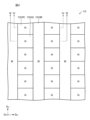
- FIG. 1 is a plan view showing an example of the configuration of the display device according to the first embodiment.
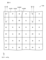
- FIG. 2 is a plan view showing an enlarged part of the display area of the display device according to the first embodiment.
- FIG. 3 is a cross-sectional view taken along line III--III in FIG.
- FIG. 4 is a cross-sectional view taken along line IV--IV of FIG.
- FIG. 5 is a process chart for explaining an example of the method for manufacturing the display device according to the first embodiment.
- FIG. 6 is a process chart for explaining an example of the method for manufacturing the display device according to the first embodiment.
- FIG. 7 is a process chart for explaining an example of the method for manufacturing the display device according to the first embodiment.
- FIG. 8 is a process chart for explaining an example of the method for manufacturing the display device according to the first embodiment.
- FIG. 9 is a process chart for explaining an example of the method for manufacturing the display device according to the first embodiment.
- FIG. 10 is a plan view showing an enlarged part of the display area of the display device according to the second embodiment.
- 11 is a cross-sectional view taken along line XI-XI of FIG. 10.
- FIG. 12 is a cross-sectional view taken along line XII--XII in FIG. 10.
- FIG. 13 is a plan view showing an enlarged part of the display area of the display device according to the third embodiment.
- 14 is a cross-sectional view taken along line XIV--XIV in FIG. 13.
- FIG. 15 is a plan view showing an enlarged part of the display area of the display device according to the modification.
- FIG. 16 is a plan view showing an enlarged part of the display area of the display device according to the modification.
- FIG. 17A is a front view showing an example of the appearance of a digital still camera.
- FIG. 17B is a rear view showing an example of the appearance of the digital still camera.
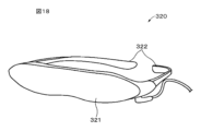
- FIG. 18 is a perspective view of an example of the appearance of a head mounted display.
- FIG. 19 is a perspective view showing an example of the appearance of the television device.
- FIG. 1 is a plan view showing an example of the configuration of a display device 10 according to the first embodiment.
- the display device 10 has a display region R1 and a peripheral region R2 provided around the display region R1.
- the display area R1 has a rectangular shape in plan view.
- a planar view means a planar view when an object is seen from a direction D P (hereinafter referred to as “perpendicular direction D P ”) perpendicular to the display surface of the display device 10 .
- a direction parallel to the long sides of the display region R1 is called a horizontal direction DH
- a direction parallel to the short sides of the display region R1 is called a vertical direction DV .
- FIG. 2 is a plan view showing an enlarged part of the display area R1 of the display device 10 according to the first embodiment.
- a plurality of sub-pixels 100R, 100G, and 100B are two-dimensionally arranged in a prescribed arrangement pattern within the display region R1.
- the peripheral region R2 is provided with a pad portion 11a, a driver (not shown) for image display, and the like.
- a flexible printed circuit (FPC) (not shown) may be connected to the pad portion 11a.
- the sub-pixel 100R can emit red light.
- the sub-pixel 100G can emit green light.
- the sub-pixel 100B can emit blue light. Red is an example of the first of the three primary colors. Green is an example of the second of the three primary colors. Blue is an example of the third primary color of the three primary colors.
- blocks marked with symbols "R", "G", and "B" represent the sub-pixel 100R, the sub-pixel 100G, and the sub-pixel 100B, respectively.
- the sub-pixels 100R, 100G, and 100B are collectively referred to as the sub-pixel 100 without any particular distinction.
- One pixel (one pixel) is composed of a combination of three sub-pixels 100R, 100G, and 100B adjacent to each other in the horizontal direction D H (row direction) of the display surface.
- the sub-pixel 100B has a linear shape extending in the vertical direction DV in plan view.
- the sub-pixels 100R and 100G are dot-shaped.
- the sub-pixels 100R, 100G, and 100B have, for example, a square shape such as a rectangular shape in plan view. In this specification, the rectangular shape includes a square shape.
- the sub-pixels 100R and 100G are alternately arranged in the vertical direction DV to form columns of sub-pixels 100R and 100G. Columns of sub-pixels 100R and 100G and linear sub-pixels 100B are alternately arranged in the horizontal direction DH .
- the pixel pitch of the sub-pixels 100R, 100G, and 100B in the horizontal direction DH is preferably 10 ⁇ m or less from the viewpoint of achieving high definition of the display device 10.
- the pixel pitch of the sub-pixels 100R and 100G in the vertical direction DP is preferably 10 ⁇ m or less from the viewpoint of achieving high definition of the display device 10.
- the display device 10 is an example of a light emitting device.
- the display device 10 is a top emission type OLED display device.
- the display device 10 may be a microdisplay.
- the display device 10 may be provided in a VR (Virtual Reality) device, an MR (Mixed Reality) device, an AR (Augmented Reality) device, an Electronic View Finder (EVF), a small projector, or the like.
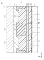
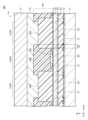
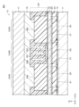
- FIG. 3 is a cross-sectional view taken along line III-III in FIG.
- FIG. 4 is a cross-sectional view taken along line IV--IV of FIG.
- the display device 10 includes a circuit board 11, a plurality of light emitting elements 20, an insulating layer 12, a protective layer 13, a planarization layer 14, a color filter 15F, a filled resin layer 16, and a counter substrate 17.
- a plurality of sub-pixels 100R, 100G, and 100B are configured by combining the color filters 15F and the light-emitting elements 20.
- FIG. 1 is a cross-sectional view taken along line III-III in FIG.
- FIG. 4 is a cross-sectional view taken along line IV--IV of FIG.
- the display device 10 includes a circuit board 11, a plurality of light emitting elements 20, an insulating layer 12, a protective layer 13, a planarization layer 14, a color filter 15F, a filled resin layer 16, and a counter substrate 17.
- the surface on the top side (display surface side) of the display device 10 is referred to as a first surface
- the bottom side (opposite side to the display surface) of the display device 10 is referred to as a first surface. is called the second surface.
- the circuit board 11 is a so-called backplane and drives the plurality of light emitting elements 20 .
- the circuit board 11 is provided with a drive circuit for driving the plurality of light emitting elements 20, a power supply circuit for supplying power to the plurality of light emitting elements 20, and the like (none of which is shown).
- the substrate body of the circuit board 11 may be composed of, for example, a semiconductor that facilitates the formation of transistors or the like, or may be composed of glass or resin with low permeability to moisture and oxygen.
- the substrate body may be a semiconductor substrate, a glass substrate, a resin substrate, or the like.
- Semiconductor substrates include, for example, amorphous silicon, polycrystalline silicon, monocrystalline silicon, or the like.
- the glass substrate includes, for example, high strain point glass, soda glass, borosilicate glass, forsterite, lead glass, quartz glass, or the like.
- the resin substrate contains, for example, at least one selected from the group consisting of polymethyl methacrylate, polyvinyl alcohol, polyvinyl phenol, polyethersulfone, polyimide, polycarbonate, polyethylene terephthalate and polyethylene naphthalate.
- the light emitting element 20 is a white OLED element, and can emit white light under control of a drive circuit or the like.
- the white OLED element may be a white Micro-OLED (MOLED) element.
- MOLED white Micro-OLED
- the plurality of light emitting elements 20 are two-dimensionally arranged on the first surface of the circuit board 11 in a prescribed arrangement pattern such as a matrix.
- the multiple light emitting elements 20 include multiple first electrodes 21 , an OLED layer 22 , and a second electrode 23 in this order on the first surface of the circuit board 11 .
- the first electrode 21 is the anode. When a voltage is applied between the first electrode 21 and the second electrode 23 , holes are injected from the first electrode 21 into the OLED layer 22 .
- the first electrodes 21 are separately provided for the plurality of light emitting elements 20 .
- the plurality of first electrodes 21 are two-dimensionally arranged on the first surface of the circuit board 11 in the same arrangement pattern as the plurality of light emitting elements 20 .
- the first electrode 21 may be composed of, for example, a metal layer, or may be composed of a metal layer and a transparent conductive oxide layer.
- the transparent conductive oxide layer is the OLED layer. It is preferably provided on the 22 side.
- the metal layer also functions as a reflective layer that reflects light emitted by the OLED layer 22 .
- the metal layer is, for example, chromium (Cr), gold (Au), platinum (Pt), nickel (Ni), copper (Cu), molybdenum (Mo), titanium (Ti), tantalum (Ta), aluminum (Al). , magnesium (Mg), iron (Fe), tungsten (W) and silver (Ag).
- the metal layer may contain the at least one metal element as a constituent element of an alloy. Specific examples of alloys include aluminum alloys and silver alloys. Specific examples of aluminum alloys include AlNd and AlCu.
- a base layer may be provided adjacent to the second surface side of the metal layer.
- the underlayer is for improving the crystal orientation of the metal layer when the metal layer is formed.
- the underlayer contains, for example, at least one metal element selected from the group consisting of titanium (Ti) and tantalum (Ta).
- the underlayer may contain the at least one metal element as a constituent element of the alloy.
- the transparent conductive oxide layer contains a transparent conductive oxide.
- Transparent conductive oxides include, for example, transparent conductive oxides containing indium (hereinafter referred to as “indium-based transparent conductive oxides”) and transparent conductive oxides containing tin (hereinafter referred to as “tin-based transparent conductive oxides”). ”) and transparent conductive oxides containing zinc (hereinafter referred to as “zinc-based transparent conductive oxides”).
- Indium-based transparent conductive oxides include, for example, indium tin oxide (ITO), indium zinc oxide (IZO), indium gallium oxide (IGO), indium gallium zinc oxide (IGZO), or fluorine-doped indium oxide (IFO).
- ITO indium tin oxide
- ITO indium tin oxide
- Tin-based transparent conductive oxides include, for example, tin oxide, antimony-doped tin oxide (ATO), or fluorine-doped tin oxide (FTO).
- Zinc-based transparent conductive oxides include, for example, zinc oxide, aluminum-doped zinc oxide (AZO), boron-doped zinc oxide, or gallium-doped zinc oxide (GZO).
- the OLED layer 22 is an example of an organic layer including a light-emitting layer.
- the OLED layer 22 can emit white light by recombination of holes injected from the first electrode 21 and electrons injected from the second electrode 23 .
- the OLED layer 22 is provided between the multiple first electrodes 21 and the second electrodes 23 .
- the OLED layer 22 is provided continuously over the plurality of light emitting elements 20 within the display region R1, and is shared by the plurality of light emitting elements 20 within the display region R1.
- the OLED layer 22 may be an OLED layer with a single-layer light emitting unit, an OLED layer with two layers of light emitting units (tandem structure), or an OLED layer with a structure other than these.
- An OLED layer comprising a single layer of light-emitting units includes, for example, a hole-injecting layer, a hole-transporting layer, a red-emitting layer, a light-emitting separating layer, a blue-emitting layer, from the first electrode 21 toward the second electrode 23 . It has a configuration in which a green light-emitting layer, an electron transport layer, and an electron injection layer are laminated in this order.
- An OLED layer comprising two layers of light-emitting units is, for example, a hole-injection layer, a hole-transport layer, a blue-light-emitting layer, an electron-transport layer, a charge-generating layer, from the first electrode 21 toward the second electrode 23 . It has a structure in which a hole transport layer, a yellow light emitting layer, an electron transport layer, and an electron injection layer are laminated in this order.
- the hole injection layer is intended to increase the efficiency of hole injection into each light-emitting layer and to suppress leakage.
- the hole-transporting layer is for increasing the efficiency of hole-transporting to each light-emitting layer.
- the electron injection layer is for increasing the efficiency of electron injection into each light-emitting layer.
- the electron transport layer is for enhancing electron transport efficiency to each light-emitting layer.
- the emission separation layer is a layer for adjusting the injection of carriers into each emission layer, and the emission balance of each color is adjusted by injecting electrons and holes into each emission layer through the emission separation layer.
- the charge generation layer supplies electrons and holes, respectively, to the two light-emitting layers sandwiching the charge generation layer.
- the second electrode 23 is the cathode. When a voltage is applied between the first electrode 21 and the second electrode 23 , electrons are injected from the second electrode 23 into the OLED layer 22 .
- the second electrode 23 is a transparent electrode having transparency to visible light. In this specification, visible light refers to light in the wavelength range of 360 nm to 830 nm.
- a second electrode 23 is provided on the first surface of the OLED layer 22 .
- the second electrode 23 is provided continuously over the plurality of light emitting elements 20 within the display region R1 and is shared by the plurality of light emitting elements 20 within the display region R1.
- the second electrode 23 is made of a material with a high transmittance and a small work function, in order to increase the luminous efficiency.
- the second electrode 23 is composed of, for example, at least one layer of a metal layer and a transparent conductive oxide layer. More specifically, the second electrode 23 is composed of a single layer film of a metal layer or a transparent conductive oxide layer, or a laminated film of a metal layer and a transparent conductive oxide layer.
- the metal layer may be provided on the OLED layer 22 side, and the transparent conductive oxide layer may be provided on the OLED layer 22 side. From the viewpoint of placing a layer having a work function adjacent to the OLED layer 22, it is preferable that the metal layer is provided on the OLED layer 22 side.
- the metal layer contains, for example, at least one metal element selected from the group consisting of magnesium (Mg), aluminum (Al), silver (Ag), calcium (Ca) and sodium (Na).
- the metal layer may contain the at least one metal element as a constituent element of an alloy. Specific examples of alloys include MgAg alloys, MgAl alloys, AlLi alloys, and the like.
- the transparent conductive oxide layer includes a transparent conductive oxide. As the transparent conductive oxide, the same material as the transparent conductive oxide of the first electrode 21 can be exemplified.
- the insulating layer 12 provides insulation between adjacent first electrodes 21 .
- the insulating layer 12 is provided on a portion of the first surface of the circuit board 11 between the separated first electrodes 21 .
- the insulating layer 12 has a plurality of openings 12a.
- a plurality of openings 12a are provided corresponding to the respective light emitting elements 20, respectively. More specifically, each of the plurality of openings 12a is provided on the first surface (surface on the OLED layer 22 side) of each first electrode 21 .
- the first electrode 21 and the OLED layer 22 are in contact with each other through the opening 12a.
- the insulating layer 12 may be an organic insulating layer, an inorganic insulating layer, or a laminate of these layers.
- the organic insulating layer contains, for example, at least one selected from the group consisting of polyimide-based resins, acrylic-based resins, novolak-based resins, and the like.
- the inorganic insulating layer contains, for example, at least one selected from the group consisting of silicon oxide (SiO x ), silicon nitride (SiN x ), silicon oxynitride (SiO x N y ), and the like.
- the protective layer 13 has transparency to visible light.
- the protective layer 13 is provided on the first surface of the second electrode 23 and covers the plurality of light emitting elements 20 .
- the protective layer 13 shields the light-emitting element 20 from the outside air and suppresses moisture from entering the light-emitting element 20 from the external environment.
- the protective layer 13 may have a function of suppressing oxidation of this metal layer.
- the protective layer 13 contains, for example, a low hygroscopic inorganic material or polymer resin.
- the protective layer 13 may have a single layer structure or a multilayer structure. When increasing the thickness of the protective layer 13, it is preferable to have a multilayer structure. This is for alleviating the internal stress in the protective layer 13 .
- the inorganic material is, for example, selected from the group consisting of silicon oxide (SiO x ), silicon nitride (SiN x ), silicon oxynitride (SiO x N y ), titanium oxide (TiO x ) and aluminum oxide (AlO x ).
- Polymer resins include, for example, at least one selected from the group consisting of thermosetting resins, ultraviolet-curable resins, and the like.
- the polymer resin includes at least one selected from the group consisting of acrylic resins, polyimide resins, novolac resins, epoxy resins, norbornene resins, and the like.
- the planarizing layer 14 is provided on the first surface of the protective layer 13 and planarizes the unevenness of the first surface of the protective layer 13 .
- the planarization layer 14 contains, for example, an inorganic material or a polymeric resin. Examples of the inorganic material include materials similar to those of the protective layer 13 .
- the polymer resin the same material as that of the protective layer 13 can be exemplified.
- the color filter 15F is an on-chip color filter (OCCF).
- OCCF on-chip color filter
- a color filter 15 ⁇ /b>F is provided above the plurality of light emitting elements 20 . More specifically, the color filter 15F is provided on the first surface of the planarization layer 14.
- the color filter 15F includes, for example, a plurality of red filter portions 15R, a plurality of green filter portions 15G, and a plurality of blue filter portions 15B.
- the red filter section 15R, the green filter section 15G, and the blue filter section 15B are collectively referred to as the filter section 15 without particular distinction.
- the plurality of filter portions 15 are two-dimensionally arranged in the in-plane direction.
- the in-plane direction means the in-plane direction on the first surface of the circuit board 11 .
- Each filter section 15 is provided above the light emitting element 20 .
- a sub-pixel 100R is composed of a red filter portion 15R and a light emitting element 20.
- a sub-pixel 100G is composed of a green filter portion 15G and a light emitting element 20.
- the sub-pixel 100B is composed of a blue filter portion 15B and a light emitting element 20. As shown in FIG.
- the red filter portion 15R transmits red light out of the white light emitted from the light emitting element 20, but absorbs light other than red light.
- the green filter portion 15G transmits green light out of the white light emitted from the light emitting element 20, but absorbs light other than green light.
- the blue filter portion 15B transmits blue light out of the white light emitted from the light emitting element 20, but absorbs light other than blue light.
- the blue filter portion 15B has a linear shape extending in the vertical direction DV in plan view.
- the red filter portion 15R and the green filter portion 15G have a dot shape in plan view, similarly to the sub-pixel 100R and the sub-pixel 100G.
- the red filter portion 15R and the green filter portion 15G have, for example, a square shape such as a rectangular shape in plan view.
- At least one color filter portion 15 among the blue filter portion 15B, the green filter portion 15G and the red filter portion 15R includes a transparent resin 150 at the bottom of the filter portion 15 .
- one of the blue filter portion 15B, the green filter portion 15G, and the red filter portion 15R may include the transparent resin 150 at the bottom of the filter portion 15, or the blue filter portion 15B may include the transparent resin 150.
- the green filter portion 15G and the red filter portion 15R the two color filter portions 15 may include the transparent resin 150 at the bottom portion of the filter portion 15, or the blue filter portion 15B, the green filter portion 15G and the red filter portion 15R. may include transparent resin 150 at the bottom of the filter portion 15 .
- the filter portion 15 may include the transparent resin 150 in a portion of the bottom portion of the filter portion 15 , or may include the transparent resin 150 in substantially the entire bottom portion of the filter portion 15 .
- the blue filter portion 15B includes a transparent resin 150 at the bottom of the blue filter portion 15B.
- the transparent resin 150 may extend over a plurality of light emitting elements 20 in the vertical direction DV , or may be divided between adjacent light emitting elements 20 .
- the transparent resin 150 bonds the bottom portion of the color filter 15F and the planarization layer 14 together, and can suppress the peeling of the color filter 15F from the planarization layer 14 .
- the transparent resin 150 preferably has transparency to visible light. Since the transparent resin 150 has transparency to visible light, it is possible to suppress absorption of the white light emitted from the light emitting element 20 by the transparent resin 150 . Therefore, a decrease in brightness of the display device 10 can be suppressed.
- the transparent resin 150 may have a layered shape. That is, the transparent resin 150 may form a transparent resin layer on the bottom of the filter section 15 .
- the transparent resin 150 is not limited to a layered shape, and may be granular or irregularly shaped.
- the filter part 15 may contain one or more granular transparent resins 150 at the bottom, or may contain one or more amorphous transparent resins 150 .
- the filter part 15 may contain at least one selected from the group consisting of the layered transparent resin 150, the granular transparent resin 150, and the amorphous transparent resin 150 in the bottom part.
- the transparent resin 150 preferably contains a thermosetting resin.
- the thermosetting resin includes, for example, thermosetting organic resin such as epoxy resin.
- the transparent resin 150 and the filled resin layer 16 preferably contain materials with the same components. Since the transparent resin 150 and the filling resin layer 16 contain materials of the same component, the transparent resin 150 is allowed to permeate the color filter 15F and harden to form the filling resin layer 16. can exist in That is, the transparent resin 150 allows the color filter 15F and the flattening layer 14 to be attached together.
- thermosetting resin includes, for example, thermosetting organic resin such as epoxy resin.
- thermosetting resin for forming the filling resin layer 16 is permeated into the color filter 15F and cured in the baking process described later, thereby making the resin transparent.
- a resin 150 can be present at the bottom of the color filter 15F. That is, the transparent resin 150 allows the color filter 15F and the flattening layer 14 to be attached together.
- the peripheral edge portions of adjacent filter portions 15 may overlap each other. It is preferable that the filter part 15 located on the upper side in the overlap of the peripheral parts contains the transparent resin 150 at the bottom.
- the filter portion 15 located on the upper side in the overlap of the peripheral edge portions is more likely to be peeled off in the below-described baking process than the filter portion 15 located on the lower side in the overlap of the peripheral edge portions. Therefore, from the viewpoint of suppressing peeling of the color filter 15F by the transparent resin 150, it is preferable that the filter section 15 located on the upper side in the overlap of the peripheral edge contains the transparent resin 150 at the bottom.
- the peripheral portion of the filter portion 15 refers to a region having a predetermined width inward from the peripheral edge of the filter portion 15 .
- the peripheral portion of the blue filter portion 15B and the peripheral portion of the green filter portion 15G may overlap in the horizontal direction DH .
- the peripheral portion of the blue filter portion 15B may be positioned above the peripheral portion of the green filter portion 15G in the horizontal direction DH .
- the peripheral portion of the blue filter portion 15B contains the transparent resin 150 at the bottom.
- the periphery of the blue filter portion 15B and the periphery of the red filter portion 15R may overlap in the horizontal direction DH .
- the peripheral portion of the blue filter portion 15B may be positioned above the peripheral portion of the red filter portion 15R in the horizontal direction DH .
- the peripheral portion of the blue filter portion 15B contains the transparent resin 150 at the bottom.
- the periphery of the red filter portion 15R and the periphery of the green filter portion 15G may overlap in the vertical direction DV .
- the peripheral portion of the red filter portion 15R may be positioned above the peripheral portion of the green filter portion 15G in the vertical direction DV .
- the peripheral portion of the red filter portion 15R contains the transparent resin 150 at the bottom.
- the width W of the overlapping edge portions of the adjacent filter portions 15 is 0.1 ⁇ m or more and 0.5 ⁇ m or less. However, the overlapping width W of the filter portions 15 may exceed 0.5 ⁇ m. If the width of overlap between the peripheral edges differs depending on the position, the maximum value of the widths of overlap between the peripheral edges is defined as the width W of the overlap between the peripheral edges.
- the red filter portion 15R contains, for example, a red coloring agent and an ultraviolet curable resin.
- the red colorant includes, for example, at least one selected from the group consisting of red dyes and red pigments.
- the green filter section 15G contains, for example, a green coloring agent and an ultraviolet curable resin. Green coloring agents include, for example, at least one selected from the group consisting of green dyes and green pigments.
- the blue filter section 15B contains, for example, a blue colorant and an ultraviolet curable resin. Blue colorants include, for example, at least one selected from the group consisting of blue dyes and blue pigments.
- the filling resin layer 16 is provided between the color filter 15F and the opposing substrate 17. As shown in FIG.
- the filling resin layer 16 functions as an adhesive layer that bonds the color filter 15F and the counter substrate 17 together.
- the filled resin layer 16 contains, for example, a thermosetting resin.
- the thermosetting resin is preferably a transparent resin.
- the transparent resin preferably contains the same material as the transparent resin 150 contained in the bottom of the filter section 15 .
- Thermosetting resins include, for example, thermosetting organic resins such as epoxy resins.
- the filling resin layer 16 may further contain an ultraviolet curable resin.
- the counter substrate 17 seals the light emitting element 20, the color filter 15F, and the like.
- the counter substrate 17 has transparency to visible light, for example.
- the counter substrate 17 is provided on the first surface of the filling resin layer 16 and faces the circuit board 11 .
- the opposing substrate 17 is, for example, a glass substrate.
- Step of forming first electrode 21 First, a metal layer and a metal oxide layer are sequentially formed on the first surface of the circuit board 11 by, for example, a sputtering method, and then the metal layer and the metal oxide layer are patterned by, for example, a photolithography technique and an etching technique. . Thereby, a plurality of first electrodes 21 are formed on the first surface of the circuit board 11 .
- the insulating layer 12 is formed on the first surface of the circuit board 11 so as to cover the plurality of first electrodes 21 by, for example, a CVD (Chemical Vapor Deposition) method.
- openings 12a are formed in portions of the insulating layer 12 located on the first surfaces of the first electrodes 21 by photolithography and dry etching, for example.
- a hole transport layer, a red light emitting layer, a light emitting separation layer, a blue light emitting layer, a green light emitting layer, an electron transport layer, and an electron injection layer are formed on the first surface of the plurality of first electrodes 21 by vapor deposition, for example. and on the first surface of the insulating layer 12 in this order to form the OLED layer 22 .
- a second electrode 23 is formed on the first surface of the OLED layer 22 by vapor deposition or sputtering, for example. Thereby, a plurality of light emitting elements 20 are formed on the first surface of the circuit board 11 .
- the protective layer 13 is formed on the first surface of the second electrode 23 by, for example, CVD or vapor deposition.
- planarization layer 14 is formed on the first surface of the second electrode 23 by, for example, CVD or vapor deposition.
- a coloring composition for forming a green filter portion is applied onto the first surface of the planarizing layer 14, irradiated with ultraviolet rays through a photomask for pattern exposure, and then developed to form a green filter portion 15G.
- a coloring composition for forming a red filter portion is applied onto the first surface of the planarizing layer 14, and patterned exposure is performed by irradiating ultraviolet rays through a photomask, followed by development to form a red filter portion 15R.
- a coloring composition for forming a blue filter portion is applied onto the first surface of the flattening layer 14, irradiated with ultraviolet rays through a photomask for pattern exposure, and then developed to form a blue filter portion 15B. to form Thereby, a color filter 15F is formed on the first surface of the planarization layer 14, as shown in FIG.
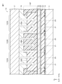
- Step of Overlapping Counter Substrate 17 Next, after covering the color filter 15F with the filling resin layer 16 using, for example, the ODF (One Drop Fill) method, as shown in FIG.
- thermosetting resin contained in the filled resin layer 16 begins to permeate the color filters 15F.
- the thermosetting resin is preferably a transparent resin. Since the blue filter portion 15B is positioned above the green filter portion 15G in the overlapping of the peripheral portions in the horizontal direction DH , when the baking process is started, as shown in FIG. On the other hand, stress (see the arrow in FIG. 8) is likely to be applied in a direction that lifts the blue filter portion 15B. Further, although not shown, the blue filter portion 15B is positioned above the red filter portion 15R in the overlapping of the peripheral portions in the horizontal direction DH . Stress is likely to be applied in a direction that lifts the portion 15B.
- a cavity 151 begins to form between the blue filter section 15B and the underlying planarization layer 14 .
- the cavities 151 are filled with a thermosetting resin that permeates the color filters 15F.
- the mold resin is cured.
- the color filter 15F and the counter substrate 17 are bonded via the filling resin layer 16 to seal the display device 10, and a transparent resin layer 150 or the like is formed on the bottom of the blue filter portion 15B.
- the phenomena shown in FIGS. 7 to 9 were explained separately for easy understanding, but the phenomena shown in FIGS. 7 to 9 may proceed simultaneously.
- the display device 10 shown in FIGS. 1 to 3 is obtained.
- the OCCF is formed above the heat-sensitive light-emitting layer. Therefore, there is a process limitation that the OCCF must be formed by a low temperature process. Therefore, in the conventional display device, sufficient heat treatment cannot be performed in the OCCF formation process, and the adhesion between the OCCF and its underlying layer (for example, a planarization layer or a protective layer) is reduced, resulting in the problem that the OCCF is easily peeled off. .
- display characteristics eg, uniformity, chromaticity, viewing angle, display surface roughness, etc.
- reliability for example, image defects due to progression of peeling of OCCF may be lowered.
- At least one color filter portion 15 among the red filter portion 15R, the green filter portion 15G and the blue filter portion 15B includes a transparent resin 150 at the bottom.
- the transparent resin 150 can bond the color filter 15F and the flattening layer 14 thereunder, thereby suppressing peeling of the color filter 15F. Therefore, deterioration of display characteristics can be suppressed.
- the transparent resin 150 since the transparent resin 150 has transparency to visible light, it is possible to suppress a decrease in brightness of the display device 10 .
- the transparent resin 150 on the bottom of the filter section 15 is baked, and the thermosetting resin for forming the filling resin layer 16 permeates the color filter 15F. , filling the cavity 151 formed at the bottom of the filter part 15, and curing. Therefore, it is possible to form a layer of the transparent resin 150 or the like on the part that is easily peeled off due to the formation of the cavity 151 .
- a layer of the transparent resin 150 or the like can be formed on the bottom portion of the filter section 15 in the baking process (sealing process) for thermally curing the filling resin layer 16 . can. Therefore, peeling of the color filter 15F can be suppressed without increasing the manufacturing process.
- the OCCF must be formed by a low-temperature process. Therefore, in conventional display devices, the adhesion between the OCCF and its underlying layer (for example, a planarizing layer or a protective layer) is poor. There is a problem that the OCCF is easily peeled off.
- As methods for suppressing peeling of the OCCF (1) a method of increasing the installation area between the OCCF and the base layer, and (2) a method of increasing the overlapping of the peripheral edge portions of the adjacent filter portions (overlap) are conceivable.
- the width W of the overlapping filter portions is preferably 0.1 ⁇ m or more and 0.5 ⁇ m or less.
- the OCCF is easily peeled off due to the stress itself of the filter portion due to the overlap.
- the overlapping width W of the filter portions 15 is 0.00. Even when the thickness exceeds 5 ⁇ m, peeling of the color filter 15F can be suppressed.
- FIG. 10 is a plan view showing an enlarged part of the display region R1 of the display device 10A according to the second embodiment.
- 11 is a cross-sectional view taken along line XI-XI of FIG. 10.
- FIG. 12 is a cross-sectional view taken along line XII--XII in FIG. 10.
- FIG. 10A instead of forming a plurality of sub-pixels 100R, 100G, and 100B (see FIGS. 2 to 4) by combining the color filters 15F and the light emitting elements 20, the color filters 15F1 and the light emitting elements 20 are combined.
- the display device 10 differs from the display device 10 according to the first embodiment in that a plurality of sub-pixels 100R, 100G, 100B1, and 100IR are configured by .
- symbol is attached
- blocks marked with symbols "R”, “G”, “B”, and "IR” represent sub-pixel 100R, sub-pixel 100G, sub-pixel 100B1, and sub-pixel 100IR, respectively.
- the sub-pixel 100B1 can emit blue light.
- the sub-pixel 100B1 has a dot shape.
- the sub-pixel 100IR has, for example, a quadrangular shape such as a rectangular shape in plan view.
- the sub-pixel 100IR can emit infrared rays.
- the sub-pixel 100IR has a dot shape.
- the sub-pixel 100IR has, for example, a quadrangular shape such as a rectangular shape in plan view.
- the sub-pixels 100B1 and 100IR are alternately arranged in the vertical direction DV to form columns of sub-pixels 100B1 and 100IR.
- the sub-pixels 100R and 100G are alternately arranged in the vertical direction DV to form columns of sub-pixels 100R and 100G.
- Columns composed of sub-pixels 100B1 and 100IR and columns composed of sub-pixels 100R and 100G are alternately arranged in the horizontal direction DH .
- the sub-pixels 100B1 and 100R are alternately arranged in the horizontal direction DH to form a row of sub-pixels 100B1 and 100R.
- the sub-pixels 100IR and 100G are alternately arranged in the horizontal direction DH to form a row of the sub-pixels 100IR and 100G.
- Rows of sub-pixels 100B1 and 100R and rows of sub-pixels 100IR and 100G are alternately arranged in the vertical direction DV .
- the color filter 15F1 includes, for example, a plurality of red filter portions 15R, a plurality of green filter portions 15G, a plurality of blue filter portions 15B1, and a plurality of infrared transmission filter portions 15IR.
- the red filter section 15R, the green filter section 15G, the blue filter section 15B1, and the infrared transmission filter section 15IR are collectively referred to as the filter section 15 without particular distinction.
- the plurality of filter portions 15 are two-dimensionally arranged in the in-plane direction. Each filter section 15 is provided above the light emitting element 20 .
- a sub-pixel 100 B 1 is composed of a blue filter portion 15 B 1 and a light emitting element 20 .
- a sub-pixel 100IR is composed of an infrared transmission filter portion 15IR and a light-emitting element 20 .
- the white light emitted from the light emitting element 20 includes infrared light (infrared (IR)).
- the blue filter section 15B1 transmits blue light, but absorbs light other than blue light.
- the infrared transmission filter portion 15IR transmits infrared light among the white light emitted from the light emitting element 20, but absorbs light other than infrared light.
- the blue filter portion 15B1 and the infrared transmission filter portion 15IR have a dot shape in plan view, like the sub-pixels 100B1 and 100IR.
- the blue filter portion 15B1 and the infrared transmission filter portion 15IR have, for example, a square shape such as a rectangular shape in plan view.
- At least one of the blue filter portion 15B1, the green filter portion 15G, the red filter portion 15R, and the infrared transmission filter portion 15IR includes a transparent resin 150 at the bottom of the filter portion 15.
- one of the blue filter portion 15B1, the green filter portion 15G, the red filter portion 15R, and the infrared transmission filter portion 15IR includes the transparent resin 150 at the bottom of the filter portion 15.
- two types of filter portions 15 out of the blue filter portion 15B1, the green filter portion 15G, the red filter portion 15R, and the infrared transmission filter portion 15IR may include the transparent resin 150 at the bottom of the filter portion 15,
- Three types of filter portions 15 out of the blue filter portion 15B1, the green filter portion 15G, the red filter portion 15R, and the infrared transmission filter portion 15IR may include the transparent resin 150 at the bottom of the filter portion 15, or the blue filter portion All of 15B1, green filter section 15G, red filter section 15R and infrared transmission filter section 15IR may include transparent resin 150 at the bottom of filter section 15 concerned.
- the infrared transmission filter portion 15IR includes the transparent resin 150 at the bottom of the infrared transmission filter portion 15IR
- the blue filter portion 15B1 includes the transparent resin 150 at the bottom of the blue filter portion 15B1.
- An example including is shown.
- the peripheral edge portions of adjacent filter portions 15 may overlap each other. It is preferable that the filter part 15 located on the upper side in the overlap of the peripheral parts contains the transparent resin 150 at the bottom.
- the peripheral portion of the infrared transmission filter portion 15IR and the peripheral portion of the green filter portion 15G may overlap in the horizontal direction DH .
- the peripheral portion of the infrared transmission filter portion 15IR may be positioned above the peripheral portion of the green filter portion 15G in the horizontal direction DH .
- the peripheral portion of the infrared transmission filter portion 15IR includes the transparent resin 150 at the bottom.
- the peripheral portion of the green filter portion 15G may be positioned above the peripheral portion of the infrared transmission filter portion 15IR in the horizontal direction DH .
- the peripheral portion of the green filter portion 15G includes the transparent resin 150 at the bottom.
- the peripheral portion of the blue filter portion 15B1 and the peripheral portion of the red filter portion 15R may overlap in the horizontal direction DH .
- the peripheral portion of the blue filter portion 15B1 may be positioned above the peripheral portion of the red filter portion 15R in the horizontal direction DH .
- the peripheral portion of the blue filter portion 15B1 includes the transparent resin 150 at the bottom.
- the periphery of the red filter portion 15R and the periphery of the green filter portion 15G may overlap in the vertical direction DV .
- the peripheral portion of the red filter portion 15R may be positioned above the peripheral portion of the green filter portion 15G in the vertical direction DV .
- the peripheral portion of the red filter portion 15R contains the transparent resin 150 at the bottom.
- the peripheral portion of the blue filter portion 15B1 and the peripheral portion of the infrared transmission filter portion 15IR may overlap in the vertical direction DV .
- the peripheral portion of the blue filter portion 15B1 may be positioned above the peripheral portion of the infrared transmission filter portion 15IR in the vertical direction DV .
- the peripheral portion of the blue filter portion 15B1 includes the transparent resin 150 at the bottom.
- the peripheral portion of the infrared transmission filter portion 15IR may be positioned above the peripheral portion of the blue filter portion 15B1 in the vertical direction DV .
- the peripheral portion of the infrared transmission filter portion 15IR includes the transparent resin 150 at the bottom.
- the blue filter section 15B1 contains, for example, a blue colorant and an ultraviolet curable resin.
- Blue colorants include, for example, at least one selected from the group consisting of blue dyes and blue pigments.
- the infrared transmission filter portion 15IR includes, for example, an infrared transmission black color material and an ultraviolet curable resin.
- At least one of the red filter portion 15R, the green filter portion 15G, the blue filter portion 15B1, and the infrared transmission filter portion 15IR has a transparent resin 150 at the bottom.
- the transparent resin 150 can bond the color filter 15F and the flattening layer 14 therebelow, thereby preventing the color filter 15F1 from peeling off.
- the function of the display device 10A can be improved by including the sub-pixel 100IR in addition to the sub-pixels 100R, 100G, and 100B1 each having three primary colors. Therefore, it is possible to improve the function of the display device 10A while suppressing peeling of the color filter 15F1.
- FIG. 13 is a plan view showing an enlarged part of the display region R1 of the display device 10B according to the third embodiment.
- 14 is a cross-sectional view taken along line XIV--XIV in FIG. 13.
- FIG. 10B instead of forming a plurality of sub-pixels 100R, 100G, 100B1, and 100IR (see FIGS. 10 to 12) by combining the color filter 15F1 and the light emitting element 20, the display device 10B includes the color filter 15F2 and the light emitting element 20. are different from the display device 10A according to the second embodiment in that a plurality of sub-pixels 100R, 100G, 100B1, and 100W are configured by combining .
- the sub-pixel 100W can emit white light.
- the sub-pixel 100W has a dot shape.
- the sub-pixel 100W has, for example, a square shape such as a rectangular shape in plan view.
- the sub-pixels 100B1 and 100W are alternately arranged in the vertical direction DV to form columns of sub-pixels 100B1 and 100W.
- the sub-pixels 100R and 100G are alternately arranged in the vertical direction DV to form columns of sub-pixels 100R and 100G.
- Columns composed of sub-pixels 100B1 and 100W and columns composed of sub-pixels 100R and 100G are alternately arranged in the horizontal direction DH .
- the sub-pixels 100B1 and 100R are alternately arranged in the horizontal direction DH to form a row of sub-pixels 100B1 and 100R.
- the sub-pixels 100W and 100G are alternately arranged in the horizontal direction DH to form a row of sub-pixels 100W and 100G. Rows of sub-pixels 100B1 and 100R and rows of sub-pixels 100W and 100G are alternately arranged in the vertical direction DV .
- the color filter 15F2 includes, for example, a plurality of red filter portions 15R, a plurality of green filter portions 15G, a plurality of blue filter portions 15B1, and a plurality of light transmission portions 15W.
- the red filter section 15R, the green filter section 15G, and the blue filter section 15B1 are collectively referred to as the filter section 15 without particular distinction.
- the plurality of filter portions 15 and the plurality of light transmission portions 15W are two-dimensionally arranged in the in-plane direction.
- Each filter section 15 is provided above the light emitting element 20 .
- Each light transmission part 15W is also provided above the light emitting element 20 .
- a sub-pixel 100W is composed of a light transmitting portion 15W and a light emitting element 20. As shown in FIG.
- the light transmitting portion 15W can transmit white light emitted from the light emitting element 20 .
- the light transmitting portion 15W is, for example, an opening penetrating in the perpendicular direction DP .
- the light transmission portion 15W has a dot shape in plan view, similar to the sub-pixels 100R, 100G, and 100B1.
- the light transmitting portion 15W has, for example, a quadrangular shape such as a rectangular shape in plan view.
- At least one color filter portion 15 among the red filter portion 15R, the green filter portion 15G and the blue filter portion 15B1 includes a transparent resin 150 at the bottom of the filter portion 15 concerned.
- one of the red filter portion 15R, the green filter portion 15G, and the blue filter portion 15B1 may include the transparent resin 150 at the bottom of the filter portion 15, or the red filter portion 15R may , the green filter portion 15G and the blue filter portion 15B1, the two color filter portions 15 may include the transparent resin 150 at the bottom portion of the filter portion 15, or the red filter portion 15R, the green filter portion 15G and the blue filter portion 15B1. may include transparent resin 150 at the bottom of the filter portion 15 .
- At least one of the red filter portion 15R, the green filter portion 15G, and the blue filter portion 15B1 includes a transparent resin 150 at the bottom.
- the color filter 15F2 and the underlying planarization layer 14 can be bonded together by the transparent resin 150, so that peeling of the color filter 15F2 can be suppressed.
- one pixel includes the sub-pixel 100W in addition to the sub-pixels 100R, 100G, and 100B1 of the three primary colors, so that the luminance of the display device 10B can be improved. Therefore, it is possible to improve the luminance of the display device 10B while suppressing peeling of the color filter 15F2.
- FIG. 15 is a plan view showing an enlarged part of the display region R1 of the display device 10C according to Modification 1.
- the display device 10C differs from the display device 10 according to the second embodiment in that one pixel is formed by combining four sub-pixels 100R, 100G, 100B1, and 100B1.
- the sub-pixels 100G and 100B1 are alternately arranged in the vertical direction DV to form columns of sub-pixels 100G and 100B1.
- the sub-pixels 100B1 and 100R are alternately arranged in the vertical direction DV to form columns of sub-pixels 100B1 and 100R.
- Columns composed of the sub-pixels 100G and 100B1 and columns composed of the sub-pixels 100B1 and 100R are alternately arranged in the horizontal direction DH .
- the sub-pixels 100G and 100B1 are alternately arranged in the horizontal direction DH to form a row of sub-pixels 100G and 100B1.
- the sub-pixels 100B1 and 100R are alternately arranged in the horizontal direction DH to form a row of sub-pixels 100B1 and 100R. Rows of sub-pixels 100G and 100B and rows of sub-pixels 100B1 and 100R are alternately arranged in the vertical direction DV .
- Modification 2 In the first embodiment, the example in which the sub-pixels 100R and 100G have a square shape in plan view and the sub-pixel 100B has a linear shape in plan view has been described. is not limited to this example.
- FIG. 16 is a plan view showing an enlarged part of the display region R1 of the display device 10D according to Modification 2.
- FIG. The display device 10D differs from the first embodiment in that sub-pixels 100R, 100G, and 100B have a hexagonal shape in plan view. Although illustration is omitted, the sub-pixels 100R, 100G, and 100B may have a circular shape or an elliptical shape in plan view, or may have a polygonal shape other than a square shape and a hexagonal shape in plan view. good.
- one pixel is composed of three sub-pixels 100 or four sub-pixels 100
- the configuration of one pixel is not limited to this example.
- one pixel may be composed of two sub-pixels 100 or five or more sub-pixels 100 .
- the color filter may include two color filter portions or five or more color filter portions.
- the color filter 15F2 includes the light transmission portion 15W and the light transmission portion 15W is an opening has been described, but the light transmission portion 15W may be a transparent filter portion.
- the transparent filter section has transparency to visible light.
- the transparent filter section contains, for example, an ultraviolet curable resin.
- the light transmitting portion 15W is a transparent filter portion
- at least one of the red filter portion 15R, the green filter portion 15G, the blue filter portion 15B1, and the transparent filter portion 15 may include a transparent resin 150 at the bottom.
- the color filter may be used for purposes such as antireflection.
- the color filter may be a monochromatic filter, may have two or more color filter portions, or may be the color filter 15F in one embodiment.
- the color filter 15F includes a plurality of red filter portions 15R, a plurality of green filter portions 15G, and a plurality of blue filter portions 15B has been described. It is not limited.
- the color filter 15F further includes at least one of a plurality of cyan filter sections and a plurality of magenta filter sections in addition to the plurality of red filter sections 15R, the plurality of green filter sections 15G, and the plurality of blue filter sections 15B.
- the cyan color filter section and the magenta color filter section are complementary color filters for adjusting colored light in the sub-pixels 100R, 100G, and 100B.
- the color filter 15F1 may further include at least one of a plurality of cyan color filter portions and a plurality of magenta color filter portions.
- the color filter 15F2 may further include at least one of a plurality of cyan color filter portions and a plurality of magenta color filter portions.
- the cavity 151 may be formed depending on the combination of 15F and its lower layer material, the material of the filling resin layer 16, or the process conditions at the time of sealing with the opposing substrate 17, or the like. Cavities 151 may be formed by a combination of two or more of the above conditions.
- the present disclosure can also employ the following configuration.
- a plurality of light emitting elements arranged two-dimensionally; a filter provided above the plurality of light emitting elements and including a plurality of color filter portions, The light-emitting device, wherein at least one color filter portion of the plurality of color filter portions includes a transparent resin at the bottom.
- the transparent resin includes a thermosetting resin.
- the transparent resin includes an epoxy-based resin.
- the light-emitting device according to any one of (1) to (8), wherein the plurality of color filter sections includes a plurality of red filter sections, a plurality of green filter sections, and a plurality of blue filter sections.
- the filter further includes a plurality of infrared transmission filter sections.
- the plurality of light emitting elements are capable of emitting white light
- the filter further includes a plurality of light transmission parts, The light-emitting device according to (9), wherein the light-transmitting portion can transmit the white light.
- the light-emitting device according to any one of (1) to (11), wherein the transparent resin is present on substantially the entire bottom portion.
- the light-emitting device according to any one of (1) to (13), wherein the transparent resin is layered.
- the light-emitting device according to any one of (1) to (14), wherein the transparent resin is granular.
- a plurality of light emitting elements arranged two-dimensionally; a filter provided above the plurality of light emitting elements, The light-emitting device, wherein the filter includes a filter portion containing a transparent resin at the bottom.
- An electronic device comprising the light emitting device according to any one of (1) to (16).
- the display devices 10, 10A, 10B, 10C, and 10D (hereinafter referred to as "display devices 10, etc.") according to the first to third embodiments and modifications thereof can be used in various electronic devices.
- the display device 10 or the like is particularly suitable for video cameras, electronic viewfinders of single-lens reflex cameras, or head-mounted displays that require high resolution and are used in close proximity to the eyes.
- FIG. 1 This digital still camera 310 is of an interchangeable single-lens reflex type, and has an interchangeable photographing lens unit (interchangeable lens) 312 in approximately the center of the front of a camera main body (camera body) 311, and on the left side of the front. It has a grip portion 313 for a photographer to hold.
- interchangeable photographing lens unit interchangeable lens
- a monitor 314 is provided at a position shifted to the left from the center of the back surface of the camera body 311 .
- An electronic viewfinder (eyepiece window) 315 is provided above the monitor 314 . By looking through the electronic viewfinder 315, the photographer can view the optical image of the subject guided from the photographing lens unit 312 and determine the composition.
- the electronic viewfinder 315 includes any one of the display device 10 and the like.
- FIG. 18 shows an example of the appearance of the head mounted display 320.
- the head-mounted display 320 has, for example, ear hooks 322 on both sides of an eyeglass-shaped display 321 to be worn on the user's head.
- the display unit 321 includes any one of the display device 10 and the like.
- FIG. 19 shows an example of the appearance of the television device 330.
- the television apparatus 330 has, for example, an image display screen portion 331 including a front panel 332 and a filter glass 333, and the image display screen portion 331 includes any one of the display device 10 and the like.
Abstract
Provided is a light-emitting device capable of suppressing peeling of a color filter. The light-emitting device comprises: a plurality of light-emitting elements disposed two-dimensionally; and a filter provided above the plurality of light-emitting elements and including filter parts of a plurality of colors. At least a filter part of one color among the filter parts of the plurality of colors contains a transparent resin at the bottom part thereof.
Description
本開示は、発光装置およびそれを備える電子機器に関する。
The present disclosure relates to a light-emitting device and an electronic device including the same.
複数のOLED(Organic Light Emitting Diode)素子が2次元配置された発光装置は、広く普及している。従来の発光装置では、カラーフィルタは、複数のOLED素子が配置された基板とは別の基板に設けられていた。しかしながら、このような構成の発光装置では、発光装置の製造工程において発光素子とカラーフィルタの位置ズレが発生し色度がずれやすく、またOLED素子とカラーフィルタの間の距離が遠く、光の利用効率が低くなるという問題があった。
Light-emitting devices in which multiple OLED (Organic Light Emitting Diode) elements are two-dimensionally arranged are widely used. In conventional light-emitting devices, color filters are provided on a substrate different from the substrate on which the plurality of OLED elements are arranged. However, in the light-emitting device having such a configuration, misalignment occurs between the light-emitting element and the color filter during the manufacturing process of the light-emitting device, and the chromaticity tends to deviate. There was a problem of low efficiency.
近年の発光装置では、上記の問題を回避するため、OLED素子と同一の基板上にカラーフィルタが設けられたオンチップカラーフィルタ(On Chip Color Filter:OCCF)構造が主流になっている(例えば特許文献1参照)。
In recent years, in order to avoid the above problem, an on-chip color filter (OCCF) structure in which a color filter is provided on the same substrate as an OLED element has become mainstream (for example, patent Reference 1).
しかしながら、OCCF構造の発光装置では、カラーフィルタが剥がれることがある。カラーフィルタの剥がれが発生すると、発光装置の表示特性が低下する虞がある。
However, in a light-emitting device with an OCCF structure, the color filter may peel off. When the color filter peels off, the display characteristics of the light-emitting device may deteriorate.
本開示の目的は、カラーフィルタの剥がれを抑制することができる発光装置およびそれを備える電子機器を提供することにある。
An object of the present disclosure is to provide a light-emitting device capable of suppressing peeling of color filters and an electronic device including the same.
上記の課題を解決するために、本開示に係る発光装置は、
2次元配置された複数の発光素子と、
複数の発光素子の上方に設けられ、複数色のフィルタ部を含むフィルタと
を備え、
複数色のフィルタ部のうち少なくとも1色のフィルタ部は、底部に透明樹脂を含む。 In order to solve the above problems, the light-emitting device according to the present disclosure includes
a plurality of light emitting elements arranged two-dimensionally;
a filter provided above the plurality of light emitting elements and including a plurality of color filter portions,
At least one color filter portion of the plurality of color filter portions contains a transparent resin at the bottom.
本開示に係る発光装置は、
2次元配置された複数の発光素子と、
複数の発光素子の上方に設けられたフィルタと
を備え、
フィルタは、底部に透明樹脂を含むフィルタ部を含む。 The light-emitting device according to the present disclosure is
a plurality of light emitting elements arranged two-dimensionally;
and a filter provided above the plurality of light emitting elements,
The filter includes a filter portion containing transparent resin at the bottom.
本開示に係る電子機器は、本開示に係る発光装置を備える。
An electronic device according to the present disclosure includes the light emitting device according to the present disclosure.
本開示において、複数色のフィルタ部は、3色のフィルタ部を含んでもよい。3色のフィルタ部のうち1色のフィルタ部が底部に透明樹脂を含んでもよいし、3色のフィルタ部のうち2色のフィルタ部が底部に透明樹脂を含んでもよいし、3色のフィルタ部が底部に透明樹脂を含んでもよい。
In the present disclosure, the multiple-color filter section may include three-color filter sections. One of the three-color filter sections may contain a transparent resin at the bottom, two of the three-color filter sections may contain a transparent resin at the bottom, or the three-color filter may contain transparent resin at the bottom. The part may contain a transparent resin on the bottom.
本開示において、複数色のフィルタ部は、赤色フィルタ部と、緑色フィルタ部と、青色フィルタ部の3色のフィルタ部を含んでもよい。
3色のフィルタ部のうち赤色フィルタ部が底部に透明樹脂を含んでもよいし、3色のフィルタ部のうち緑色フィルタ部が底部に透明樹脂を含んでもよいし、3色のフィルタ部のうち青色フィルタ部が底部に透明樹脂を含んでもよい。
3色のフィルタ部のうち赤色フィルタ部および緑色フィルタ部が底部に透明樹脂を含んでもよいし、3色のフィルタ部のうち赤色フィルタ部および青色フィルタ部が底部に透明樹脂を含んでもよいし、3色のフィルタ部のうち緑色フィルタ部および青色フィルタ部が底部に透明樹脂を含んでもよい。
3色のフィルタ部、すなわち赤色フィルタ部、緑色フィルタ部および青色フィルタ部が底部に透明樹脂を含んでもよい。 In the present disclosure, the multi-color filter section may include three color filter sections, a red filter section, a green filter section, and a blue filter section.
Of the three-color filter portions, the red filter portion may include a transparent resin at the bottom, the green filter portion of the three-color filter portions may include a transparent resin at the bottom, and the blue filter portion of the three-color filter portions may include a transparent resin at the bottom. The filter part may contain a transparent resin at the bottom.
The red filter part and the green filter part among the three color filter parts may contain a transparent resin at the bottom, the red filter part and the blue filter part among the three color filter parts may contain a transparent resin at the bottom, Of the three color filter parts, the green filter part and the blue filter part may contain a transparent resin at the bottom.
The three color filter parts, namely the red filter part, the green filter part and the blue filter part, may contain a transparent resin at the bottom.
本開示において、フィルタは、3色のフィルタ部と、赤外透過フィルタ部との4種のフィルタ部を含んでもよい。4種のフィルタ部のうち1種のフィルタ部が底部に透明樹脂を含んでもよいし、4種のフィルタ部のうち2種のフィルタ部が底部に透明樹脂を含んでもよいし、4種のフィルタ部のうち3種のフィルタ部が底部に透明樹脂を含んでもよいし、4種のフィルタ部が底部に透明樹脂を含んでもよい。
In the present disclosure, the filter may include four types of filter sections, ie, a three-color filter section and an infrared transmission filter section. One of the four types of filter sections may contain a transparent resin in the bottom, two of the four types of filter sections may contain a transparent resin in the bottom, or four types of filters may be used. Of the parts, three types of filter sections may contain a transparent resin on the bottom, and four types of filter sections may contain a transparent resin on the bottom.
本開示において、フィルタは、赤色フィルタ部と、緑色フィルタ部と、青色フィルタ部と、赤外透過フィルタ部との4種のフィルタ部を含んでもよい。
4種のフィルタ部のうち赤色フィルタ部が底部に透明樹脂を含んでもよいし、4種のフィルタ部のうち緑色フィルタ部が底部に透明樹脂を含んでもよいし、4種のフィルタ部のうち青色フィルタ部が底部に透明樹脂を含んでもよいし、4種のフィルタ部のうち赤外透過フィルタ部が底部に透明樹脂を含んでもよい。
4種のフィルタ部のうち赤色フィルタ部および緑色フィルタ部が底部に透明樹脂を含んでもよいし、4種のフィルタ部のうち赤色フィルタ部および青緑色フィルタ部が底部に透明樹脂を含んでもよいし、4種のフィルタ部のうち赤色フィルタ部および赤外透過フィルタ部が底部に透明樹脂を含んでもよいし、4種のフィルタ部のうち緑色フィルタ部および青色フィルタ部が底部に透明樹脂を含んでもよいし、4種のフィルタ部のうち緑色フィルタ部および赤外透過フィルタ部が底部に透明樹脂を含んでもよいし、4種のフィルタ部のうち青色フィルタ部および赤外透過フィルタ部が底部に透明樹脂を含んでもよい。
4種のフィルタ部のうち赤色フィルタ部、緑色フィルタ部および青色フィルタ部が底部に透明樹脂を含んでもよいし、4種のフィルタ部のうち赤色フィルタ部、緑色フィルタ部および赤外透過フィルタ部が底部に透明樹脂を含んでもよいし、4種のフィルタ部のうち赤色フィルタ部、青色フィルタ部および赤外透過フィルタ部が底部に透明樹脂を含んでもよいし、4種のフィルタ部のうち緑色フィルタ部、青色フィルタ部および赤外透過フィルタ部が底部に透明樹脂を含んでもよい。
4種のフィルタ部、すなわち赤色フィルタ部、緑色フィルタ部、青色フィルタ部および赤外透過フィルタ部が底部に透明樹脂を含んでもよい。 In the present disclosure, the filter may include four types of filter units: a red filter unit, a green filter unit, a blue filter unit, and an infrared transmission filter unit.
Among the four types of filter sections, the red filter section may contain a transparent resin at the bottom, the green filter section among the four types of filter sections may contain a transparent resin at the bottom, and the blue filter section among the four types may contain a transparent resin at the bottom. The filter part may contain transparent resin in the bottom part, or the infrared transmission filter part among the four types of filter parts may contain transparent resin in the bottom part.
Of the four types of filter sections, the red filter section and the green filter section may contain a transparent resin on the bottom, or the red filter section and the blue-green filter section of the four types of filter sections may contain a transparent resin on the bottom. Of the four types of filter sections, the red filter section and the infrared transmission filter section may contain transparent resin on the bottom, or the green filter section and the blue filter section of the four types of filter sections may contain transparent resin on the bottom. Alternatively, the green filter portion and the infrared transmission filter portion among the four types of filter portions may contain a transparent resin on the bottom, and the blue filter portion and the infrared transmission filter portion among the four types of filter portions may contain a transparent resin on the bottom. It may contain a resin.
Of the four types of filter sections, the red filter section, the green filter section, and the blue filter section may include a transparent resin at the bottom. A transparent resin may be included in the bottom portion, or the red filter portion, the blue filter portion, and the infrared transmission filter portion among the four types of filter portions may include the transparent resin in the bottom portion, or the green filter portion may include the transparent resin in the bottom portion. The bottom portion of the portion, the blue filter portion and the infrared transmission filter portion may contain a transparent resin.
Four kinds of filter parts, ie, a red filter part, a green filter part, a blue filter part and an infrared transmission filter part, may contain a transparent resin at the bottom.
本開示において、フィルタは、赤色フィルタ部と、緑色フィルタ部と、青色フィルタ部と、シアン色フィルタ部との4色のフィルタ部を含んでもよい。4色のフィルタ部のうち1色のフィルタ部が底部に透明樹脂を含んでもよいし、4色のフィルタ部のうち2色のフィルタ部が底部に透明樹脂を含んでもよいし、4色のフィルタ部のうち3色のフィルタ部が底部に透明樹脂を含んでもよいし、4色のフィルタ部が底部に透明樹脂を含んでもよい。
In the present disclosure, the filter may include four color filter sections, ie, a red filter section, a green filter section, a blue filter section, and a cyan filter section. One of the four color filter portions may contain a transparent resin at the bottom, two of the four color filter portions may contain a transparent resin at the bottom, or four color filters may be included. Of the parts, the filter parts of three colors may contain a transparent resin on the bottom, and the filter parts of four colors may contain a transparent resin on the bottom.
本開示において、フィルタは、赤色フィルタ部と、緑色フィルタ部と、青色フィルタ部と、マゼンタ色フィルタ部との4色のフィルタ部を含んでもよい。4色のフィルタ部のうち1色のフィルタ部が底部に透明樹脂を含んでもよいし、4色のフィルタ部のうち2色のフィルタ部が底部に透明樹脂を含んでもよいし、4色のフィルタ部のうち3色のフィルタ部が底部に透明樹脂を含んでもよいし、4色のフィルタ部が底部に透明樹脂を含んでもよい。
In the present disclosure, the filter may include four color filter sections, a red filter section, a green filter section, a blue filter section, and a magenta filter section. One of the four color filter portions may contain a transparent resin at the bottom, two of the four color filter portions may contain a transparent resin at the bottom, or four color filters may be included. Of the parts, the filter parts of three colors may contain a transparent resin on the bottom, and the filter parts of four colors may contain a transparent resin on the bottom.
本開示において、フィルタは、赤色フィルタ部と、緑色フィルタ部と、青色フィルタ部と、シアン色フィルタ部と、マゼンタ色フィルタ部との5色のフィルタ部を含んでもよい。5色のフィルタ部のうち1色のフィルタ部が底部に透明樹脂を含んでもよいし、5色のフィルタ部のうち2色のフィルタ部が底部に透明樹脂を含んでもよいし、5色のフィルタ部のうち3色のフィルタ部が底部に透明樹脂を含んでもよいし、5色のフィルタ部のうち4色のフィルタ部が底部に透明樹脂を含んでもよいし、5色のフィルタ部が底部に透明樹脂を含んでもよい。
In the present disclosure, the filter may include five color filter units, a red filter unit, a green filter unit, a blue filter unit, a cyan filter unit, and a magenta filter unit. One of the five-color filter portions may contain a transparent resin at the bottom, two of the five-color filter portions may contain a transparent resin at the bottom, or the five-color filters may contain a transparent resin at the bottom. 3 color filter portions may contain a transparent resin in the bottom portion, 4 color filter portions out of the 5 color filter portions may contain a transparent resin in the bottom portion, or 5 color filter portions may contain a transparent resin in the bottom portion. It may contain a transparent resin.
本開示において、フィルタは、シアン色フィルタ部と、マゼンタ色フィルタ部との2色のフィルタ部を含んでもよい。2色のフィルタ部のうち1色のフィルタ部が底部に透明樹脂を含んでもよいし、2色のフィルタ部が底部に透明樹脂を含んでもよい。
In the present disclosure, the filter may include two color filter portions, ie, a cyan color filter portion and a magenta color filter portion. Of the two-color filter portions, one-color filter portion may include a transparent resin in the bottom portion, and two-color filter portions may include a transparent resin in the bottom portion.
本開示において、表示領域に含まれる複数の特定色フィルタ部のうちの一部のフィルタ部が、底部に透明樹脂を含んでもよいし、表示領域に含まれる複数の特定色フィルタ部がすべて、底部に透明樹脂を含んでもよい。
In the present disclosure, some of the plurality of specific color filter sections included in the display area may include a transparent resin at the bottom, and all of the plurality of specific color filter sections included in the display area may include the bottom section. may contain a transparent resin.
本開示において、透明樹脂は、フィルタ部の底部の一部分に存在してもよいし、フィルタ部の底部の略全体に存在してもよい。本開示において、透明樹脂の形状は特に限定されるものではなく、例えば、層状、粒状または不定形状であってもよい。2種以上の形状の透明樹脂が、フィルタ部の底部に存在していてもよい。
In the present disclosure, the transparent resin may be present in a portion of the bottom of the filter section, or may be present in substantially the entire bottom of the filter section. In the present disclosure, the shape of the transparent resin is not particularly limited, and may be layered, granular, or amorphous, for example. Two or more shapes of transparent resin may be present at the bottom of the filter portion.
本開示の実施形態について図面を参照しながら以下の順序で説明する。なお、以下の実施形態の全図においては、同一または対応する部分には同一の符号を付す。
1 第1の実施形態(表示装置の例)
2 第2の実施形態(表示装置の例)
3 第3の実施形態(表示装置の例)
4 変形例(表示装置の変形例)
5 応用例(電子機器の例) Embodiments of the present disclosure will be described in the following order with reference to the drawings. In addition, in all the drawings of the following embodiments, the same reference numerals are given to the same or corresponding parts.
1 First embodiment (example of display device)
2 Second embodiment (example of display device)
3 Third embodiment (example of display device)
4 Modification (Modification of display device)
5 Application example (example of electronic equipment)
<1 第1の実施形態>
[表示装置10の構成]
図1は、第1の実施形態に係る表示装置10の構成の一例を示す平面図である。表示装置10は、表示領域R1と、表示領域R1の周辺に設けられた周辺領域R2とを有する。表示領域R1は、平面視において長方形状を有する。本明細書において、平面視とは、表示装置10の表示面に対して垂直な方向DP(以下「垂線方向DP」という。)から対象物が見られたときの平面視を意味する。以下の説明において、表示領域R1の長辺に平行な方向を水平方向DH、表示領域R1の短辺に平行な方向を垂直方向DVという。 <1 First Embodiment>
[Configuration of display device 10]
FIG. 1 is a plan view showing an example of the configuration of adisplay device 10 according to the first embodiment. The display device 10 has a display region R1 and a peripheral region R2 provided around the display region R1. The display area R1 has a rectangular shape in plan view. In this specification, a planar view means a planar view when an object is seen from a direction D P (hereinafter referred to as “perpendicular direction D P ”) perpendicular to the display surface of the display device 10 . In the following description, a direction parallel to the long sides of the display region R1 is called a horizontal direction DH , and a direction parallel to the short sides of the display region R1 is called a vertical direction DV .
[表示装置10の構成]
図1は、第1の実施形態に係る表示装置10の構成の一例を示す平面図である。表示装置10は、表示領域R1と、表示領域R1の周辺に設けられた周辺領域R2とを有する。表示領域R1は、平面視において長方形状を有する。本明細書において、平面視とは、表示装置10の表示面に対して垂直な方向DP(以下「垂線方向DP」という。)から対象物が見られたときの平面視を意味する。以下の説明において、表示領域R1の長辺に平行な方向を水平方向DH、表示領域R1の短辺に平行な方向を垂直方向DVという。 <1 First Embodiment>
[Configuration of display device 10]
FIG. 1 is a plan view showing an example of the configuration of a
図2は、第1の実施形態に係る表示装置10の表示領域R1の一部を拡大して表す平面図である。複数のサブ画素100R、100G、100Bが、表示領域R1内に規定の配置パターンで2次元配置されている。周辺領域R2には、パッド部11aおよび映像表示用のドライバ(図示せず)等が設けられている。図示しないフレキシブルプリント配線基板(Flexible Printed Circuit:FPC)が、パッド部11aに接続されていてもよい。
FIG. 2 is a plan view showing an enlarged part of the display area R1 of the display device 10 according to the first embodiment. A plurality of sub-pixels 100R, 100G, and 100B are two-dimensionally arranged in a prescribed arrangement pattern within the display region R1. The peripheral region R2 is provided with a pad portion 11a, a driver (not shown) for image display, and the like. A flexible printed circuit (FPC) (not shown) may be connected to the pad portion 11a.
サブ画素100Rは、赤色光を発光することができる。サブ画素100Gは、緑色光を発光することができる。サブ画素100Bは、青色光を発光することができる。赤色は、3原色のうち第1の原色の一例である。緑色は、3原色のうち第2の原色の一例である。青色は、3原色のうち第3の原色の一例である。図2中にて記号「R」、「G」、「B」が付された区画はそれぞれ、サブ画素100R、サブ画素100G、サブ画素100Bを表している。
The sub-pixel 100R can emit red light. The sub-pixel 100G can emit green light. The sub-pixel 100B can emit blue light. Red is an example of the first of the three primary colors. Green is an example of the second of the three primary colors. Blue is an example of the third primary color of the three primary colors. In FIG. 2, blocks marked with symbols "R", "G", and "B" represent the sub-pixel 100R, the sub-pixel 100G, and the sub-pixel 100B, respectively.
以下の説明において、サブ画素100R、100G、100Bを特に区別せず総称する場合には、サブ画素100という。1画素(1ピクセル)は、表示面の水平方向DH(行方向)に隣接する3つのサブ画素100R、100G、100Bの組み合わせにより構成されている。
In the following description, the sub-pixels 100R, 100G, and 100B are collectively referred to as the sub-pixel 100 without any particular distinction. One pixel (one pixel) is composed of a combination of three sub-pixels 100R, 100G, and 100B adjacent to each other in the horizontal direction D H (row direction) of the display surface.
サブ画素100Bは、平面視において、垂直方向DVに延設された線状を有している。サブ画素100R、100Gは、ドット状を有している。サブ画素100R、100G、100Bは、例えば、平面視において長方形状等の四角形状を有する。本明細書において、長方形状には、正方形状も含まれるものとする。サブ画素100R、100Gは、垂直方向DVに交互に配置され、サブ画素100R、100Gの列を構成している。サブ画素100R、100Gにより構成された列と線状のサブ画素100Bとが水平方向DHに交互に配置されている。水平方向DHにおけるサブ画素100R、100G、100Bの画素ピッチは、表示装置10の高精細化の観点から、10μm以下であることが好ましい。垂線方向DPにおけるサブ画素100R、100Gの画素ピッチは、表示装置10の高精細化の観点から、10μm以下であることが好ましい。
The sub-pixel 100B has a linear shape extending in the vertical direction DV in plan view. The sub-pixels 100R and 100G are dot-shaped. The sub-pixels 100R, 100G, and 100B have, for example, a square shape such as a rectangular shape in plan view. In this specification, the rectangular shape includes a square shape. The sub-pixels 100R and 100G are alternately arranged in the vertical direction DV to form columns of sub-pixels 100R and 100G. Columns of sub-pixels 100R and 100G and linear sub-pixels 100B are alternately arranged in the horizontal direction DH . The pixel pitch of the sub-pixels 100R, 100G, and 100B in the horizontal direction DH is preferably 10 μm or less from the viewpoint of achieving high definition of the display device 10. FIG. The pixel pitch of the sub-pixels 100R and 100G in the vertical direction DP is preferably 10 μm or less from the viewpoint of achieving high definition of the display device 10. FIG.
表示装置10は、発光装置の一例である。表示装置10は、トップエミッション方式のOLED表示装置である。表示装置10は、マイクロディスプレイであってもよい。表示装置10は、VR(Virtual Reality)装置、MR(Mixed Reality)装置、AR(Augmented Reality)装置、電子ビューファインダ(Electronic View Finder:EVF)または小型プロジェクタ等に備えられてもよい。
The display device 10 is an example of a light emitting device. The display device 10 is a top emission type OLED display device. The display device 10 may be a microdisplay. The display device 10 may be provided in a VR (Virtual Reality) device, an MR (Mixed Reality) device, an AR (Augmented Reality) device, an Electronic View Finder (EVF), a small projector, or the like.
図3は、図2のIII-III線に沿った断面図である。図4は、図2のIV-IV線に沿った断面図である。表示装置10は、回路基板11と、複数の発光素子20と、絶縁層12と、保護層13と、平坦化層14と、カラーフィルタ15Fと、充填樹脂層16と、対向基板17とを備える。カラーフィルタ15Fと発光素子20との組み合わせにより、複数のサブ画素100R、100G、100Bが構成される。
FIG. 3 is a cross-sectional view taken along line III-III in FIG. FIG. 4 is a cross-sectional view taken along line IV--IV of FIG. The display device 10 includes a circuit board 11, a plurality of light emitting elements 20, an insulating layer 12, a protective layer 13, a planarization layer 14, a color filter 15F, a filled resin layer 16, and a counter substrate 17. . A plurality of sub-pixels 100R, 100G, and 100B are configured by combining the color filters 15F and the light-emitting elements 20. FIG.
以下の説明において、表示装置10を構成する各層において、表示装置10のトップ側(表示面側)となる面を第1の面といい、表示装置10のボトム側(表示面とは反対側)となる面を第2の面という。
In the following description, in each layer constituting the display device 10, the surface on the top side (display surface side) of the display device 10 is referred to as a first surface, and the bottom side (opposite side to the display surface) of the display device 10 is referred to as a first surface. is called the second surface.
(回路基板11)
回路基板11は、いわゆるバックプレーンであり、複数の発光素子20を駆動する。回路基板11には、複数の発光素子20を駆動する駆動回路、および複数の発光素子20に電力を供給する電源回路等(いずれも図示せず)が設けられている。 (circuit board 11)
Thecircuit board 11 is a so-called backplane and drives the plurality of light emitting elements 20 . The circuit board 11 is provided with a drive circuit for driving the plurality of light emitting elements 20, a power supply circuit for supplying power to the plurality of light emitting elements 20, and the like (none of which is shown).
回路基板11は、いわゆるバックプレーンであり、複数の発光素子20を駆動する。回路基板11には、複数の発光素子20を駆動する駆動回路、および複数の発光素子20に電力を供給する電源回路等(いずれも図示せず)が設けられている。 (circuit board 11)
The
回路基板11の基板本体は、例えば、トランジスタ等の形成が容易な半導体で構成されていてもよいし、水分および酸素の透過性が低いガラスまたは樹脂で構成されていてもよい。具体的には、基板本体は、半導体基板、ガラス基板または樹脂基板等であってもよい。半導体基板は、例えば、アモルファスシリコン、多結晶シリコンまたは単結晶シリコン等を含む。ガラス基板は、例えば、高歪点ガラス、ソーダガラス、ホウケイ酸ガラス、フォルステライト、鉛ガラスまたは石英ガラス等を含む。樹脂基板は、例えば、ポリメチルメタクリレート、ポリビニルアルコール、ポリビニルフェノール、ポリエーテルスルホン、ポリイミド、ポリカーボネート、ポリエチレンテレフタラートおよびポリエチレンナフタレート等からなる群より選ばれた少なくとも1種を含む。
The substrate body of the circuit board 11 may be composed of, for example, a semiconductor that facilitates the formation of transistors or the like, or may be composed of glass or resin with low permeability to moisture and oxygen. Specifically, the substrate body may be a semiconductor substrate, a glass substrate, a resin substrate, or the like. Semiconductor substrates include, for example, amorphous silicon, polycrystalline silicon, monocrystalline silicon, or the like. The glass substrate includes, for example, high strain point glass, soda glass, borosilicate glass, forsterite, lead glass, quartz glass, or the like. The resin substrate contains, for example, at least one selected from the group consisting of polymethyl methacrylate, polyvinyl alcohol, polyvinyl phenol, polyethersulfone, polyimide, polycarbonate, polyethylene terephthalate and polyethylene naphthalate.
(発光素子20)
発光素子20は、白色OLED素子であり、駆動回路等の制御に基づき、白色光を発光することができる。白色OLED素子は、白色Micro-OLED(MOLED)素子であってもよい。表示装置10におけるカラー化の方式としては、白色OLED素子とカラーフィルタ15Fとを用いる方式が用いられる。 (Light emitting element 20)
Thelight emitting element 20 is a white OLED element, and can emit white light under control of a drive circuit or the like. The white OLED element may be a white Micro-OLED (MOLED) element. As a method of colorization in the display device 10, a method using a white OLED element and a color filter 15F is used.
発光素子20は、白色OLED素子であり、駆動回路等の制御に基づき、白色光を発光することができる。白色OLED素子は、白色Micro-OLED(MOLED)素子であってもよい。表示装置10におけるカラー化の方式としては、白色OLED素子とカラーフィルタ15Fとを用いる方式が用いられる。 (Light emitting element 20)
The
複数の発光素子20は、マトリクス状等の規定の配置パターンで回路基板11の第1の面上に2次元配置されている。複数の発光素子20は、複数の第1の電極21と、OLED層22と、第2の電極23とを順に回路基板11の第1の面上に備える。
The plurality of light emitting elements 20 are two-dimensionally arranged on the first surface of the circuit board 11 in a prescribed arrangement pattern such as a matrix. The multiple light emitting elements 20 include multiple first electrodes 21 , an OLED layer 22 , and a second electrode 23 in this order on the first surface of the circuit board 11 .
(第1の電極21)
第1の電極21は、アノードである。第1の電極21と第2の電極23の間に電圧が加えられると、第1の電極21からOLED層22にホールが注入される。第1の電極21は、複数の発光素子20で別々に設けられている。複数の第1の電極21は、複数の発光素子20と同様の配置パターンで回路基板11の第1の面上に2次元配置されている。 (First electrode 21)
Thefirst electrode 21 is the anode. When a voltage is applied between the first electrode 21 and the second electrode 23 , holes are injected from the first electrode 21 into the OLED layer 22 . The first electrodes 21 are separately provided for the plurality of light emitting elements 20 . The plurality of first electrodes 21 are two-dimensionally arranged on the first surface of the circuit board 11 in the same arrangement pattern as the plurality of light emitting elements 20 .
第1の電極21は、アノードである。第1の電極21と第2の電極23の間に電圧が加えられると、第1の電極21からOLED層22にホールが注入される。第1の電極21は、複数の発光素子20で別々に設けられている。複数の第1の電極21は、複数の発光素子20と同様の配置パターンで回路基板11の第1の面上に2次元配置されている。 (First electrode 21)
The
第1の電極21は、例えば、金属層により構成されていてもよいし、金属層と透明導電性酸化物層により構成されていてもよい。第1の電極21が金属層と透明導電性酸化物層により構成されている場合には、高い仕事関数を有する層をOLED層22に隣接させる観点からすると、透明導電性酸化物層がOLED層22側に設けられることが好ましい。
The first electrode 21 may be composed of, for example, a metal layer, or may be composed of a metal layer and a transparent conductive oxide layer. When the first electrode 21 is composed of a metal layer and a transparent conductive oxide layer, from the viewpoint of placing a layer having a high work function adjacent to the OLED layer 22, the transparent conductive oxide layer is the OLED layer. It is preferably provided on the 22 side.
金属層は、OLED層22で発光された光を反射する反射層としての機能も有している。金属層は、例えば、クロム(Cr)、金(Au)、白金(Pt)、ニッケル(Ni)、銅(Cu)、モリブデン(Mo)、チタン(Ti)、タンタル(Ta)、アルミニウム(Al)、マグネシウム(Mg)、鉄(Fe)、タングステン(W)および銀(Ag)からなる群より選ばれた少なくとも1種の金属元素を含む。金属層は、上記少なくとも1種の金属元素を合金の構成元素として含んでいてもよい。合金の具体例としては、アルミニウム合金または銀合金が挙げられる。アルミニウム合金の具体例としては、例えば、AlNdまたはAlCuが挙げられる。
The metal layer also functions as a reflective layer that reflects light emitted by the OLED layer 22 . The metal layer is, for example, chromium (Cr), gold (Au), platinum (Pt), nickel (Ni), copper (Cu), molybdenum (Mo), titanium (Ti), tantalum (Ta), aluminum (Al). , magnesium (Mg), iron (Fe), tungsten (W) and silver (Ag). The metal layer may contain the at least one metal element as a constituent element of an alloy. Specific examples of alloys include aluminum alloys and silver alloys. Specific examples of aluminum alloys include AlNd and AlCu.
下地層(図示せず)が、金属層の第2の面側に隣接して設けられていてもよい。下地層は、金属層の成膜時に、金属層の結晶配向性を向上させるためのものである。下地層は、例えば、チタン(Ti)およびタンタル(Ta)からなる群より選ばれた少なくとも1種の金属元素を含む。下地層は、上記少なくとも1種の金属元素を合金の構成元素として含んでいてもよい。
A base layer (not shown) may be provided adjacent to the second surface side of the metal layer. The underlayer is for improving the crystal orientation of the metal layer when the metal layer is formed. The underlayer contains, for example, at least one metal element selected from the group consisting of titanium (Ti) and tantalum (Ta). The underlayer may contain the at least one metal element as a constituent element of the alloy.
透明導電性酸化物層は、透明導電性酸化物を含む。透明導電性酸化物は、例えば、インジウムを含む透明導電性酸化物(以下「インジウム系透明導電性酸化物」という。)、錫を含む透明導電性酸化物(以下「錫系透明導電性酸化物」という。)および亜鉛を含む透明導電性酸化物(以下「亜鉛系透明導電性酸化物」という。)からなる群より選ばれた少なくとも1種を含む。
The transparent conductive oxide layer contains a transparent conductive oxide. Transparent conductive oxides include, for example, transparent conductive oxides containing indium (hereinafter referred to as "indium-based transparent conductive oxides") and transparent conductive oxides containing tin (hereinafter referred to as "tin-based transparent conductive oxides"). ”) and transparent conductive oxides containing zinc (hereinafter referred to as “zinc-based transparent conductive oxides”).
インジウム系透明導電性酸化物は、例えば、酸化インジウム錫(ITO)、酸化インジウム亜鉛(IZO)、酸化インジウムガリウム(IGO)、酸化インジウムガリウム亜鉛(IGZO)またはフッ素ドープ酸化インジウム(IFO)を含む。これらの透明導電性酸化物のうちでも酸化インジウム錫(ITO)が特に好ましい。酸化インジウム錫(ITO)は、仕事関数的にOLED層22へのホール注入障壁が特に低いため、表示装置10の駆動電圧を特に低電圧化することができるからである。錫系透明導電性酸化物は、例えば、酸化錫、アンチモンドープ酸化錫(ATO)またはフッ素ドープ酸化錫(FTO)を含む。亜鉛系透明導電性酸化物は、例えば、酸化亜鉛、アルミニウムドープ酸化亜鉛(AZO)、ホウ素ドープ酸化亜鉛またはガリウムドープ酸化亜鉛(GZO)を含む。
Indium-based transparent conductive oxides include, for example, indium tin oxide (ITO), indium zinc oxide (IZO), indium gallium oxide (IGO), indium gallium zinc oxide (IGZO), or fluorine-doped indium oxide (IFO). Among these transparent conductive oxides, indium tin oxide (ITO) is particularly preferred. This is because indium tin oxide (ITO) has a particularly low hole injection barrier to the OLED layer 22 in terms of work function, so that the driving voltage of the display device 10 can be particularly reduced. Tin-based transparent conductive oxides include, for example, tin oxide, antimony-doped tin oxide (ATO), or fluorine-doped tin oxide (FTO). Zinc-based transparent conductive oxides include, for example, zinc oxide, aluminum-doped zinc oxide (AZO), boron-doped zinc oxide, or gallium-doped zinc oxide (GZO).
(OLED層22)
OLED層22は、発光層を含む有機層の一例である。OLED層22は、第1の電極21から注入された正孔と第2の電極23から注入された電子との再結合により、白色光を発光することができる。 (OLED layer 22)
TheOLED layer 22 is an example of an organic layer including a light-emitting layer. The OLED layer 22 can emit white light by recombination of holes injected from the first electrode 21 and electrons injected from the second electrode 23 .
OLED層22は、発光層を含む有機層の一例である。OLED層22は、第1の電極21から注入された正孔と第2の電極23から注入された電子との再結合により、白色光を発光することができる。 (OLED layer 22)
The
OLED層22は、複数の第1の電極21と第2の電極23の間に設けられている。OLED層22は、表示領域R1内において複数の発光素子20に亘って連続して設けられ、表示領域R1内において複数の発光素子20に共有されている。
The OLED layer 22 is provided between the multiple first electrodes 21 and the second electrodes 23 . The OLED layer 22 is provided continuously over the plurality of light emitting elements 20 within the display region R1, and is shared by the plurality of light emitting elements 20 within the display region R1.
OLED層22は、単層の発光ユニットを備えるOLED層であってもよいし、2層の発光ユニットを備えるOLED層(タンデム構造)であってもよいし、これら以外の構造のOLED層であってもよい。単層の発光ユニットを備えるOLED層は、例えば、第1の電極21から第2の電極23に向かって、正孔注入層、正孔輸送層、赤色発光層、発光分離層、青色発光層、緑色発光層、電子輸送層、電子注入層がこの順序で積層された構成を有する。2層の発光ユニットを備えるOLED層は、例えば、第1の電極21から第2の電極23に向かって、正孔注入層、正孔輸送層、青色発光層、電子輸送層、電荷発生層、正孔輸送層、黄色発光層、電子輸送層と、電子注入層がこの順序で積層された構成を有する。
The OLED layer 22 may be an OLED layer with a single-layer light emitting unit, an OLED layer with two layers of light emitting units (tandem structure), or an OLED layer with a structure other than these. may An OLED layer comprising a single layer of light-emitting units includes, for example, a hole-injecting layer, a hole-transporting layer, a red-emitting layer, a light-emitting separating layer, a blue-emitting layer, from the first electrode 21 toward the second electrode 23 . It has a configuration in which a green light-emitting layer, an electron transport layer, and an electron injection layer are laminated in this order. An OLED layer comprising two layers of light-emitting units is, for example, a hole-injection layer, a hole-transport layer, a blue-light-emitting layer, an electron-transport layer, a charge-generating layer, from the first electrode 21 toward the second electrode 23 . It has a structure in which a hole transport layer, a yellow light emitting layer, an electron transport layer, and an electron injection layer are laminated in this order.
正孔注入層は、各発光層への正孔注入効率を高めると共に、リークを抑制するためのものである。正孔輸送層は、各発光層への正孔輸送効率を高めるためのものである。電子注入層は、各発光層への電子注入効率を高めるためのものである。電子輸送層は、各発光層への電子輸送効率を高めるためのものである。発光分離層は、各発光層へのキャリアの注入を調整するための層であり、発光分離層を介して各発光層に電子やホールが注入されることにより各色の発光バランスが調整される。電荷発生層は、電荷発生層を挟む2つの発光層に電子と正孔をそれぞれ供給する。
The hole injection layer is intended to increase the efficiency of hole injection into each light-emitting layer and to suppress leakage. The hole-transporting layer is for increasing the efficiency of hole-transporting to each light-emitting layer. The electron injection layer is for increasing the efficiency of electron injection into each light-emitting layer. The electron transport layer is for enhancing electron transport efficiency to each light-emitting layer. The emission separation layer is a layer for adjusting the injection of carriers into each emission layer, and the emission balance of each color is adjusted by injecting electrons and holes into each emission layer through the emission separation layer. The charge generation layer supplies electrons and holes, respectively, to the two light-emitting layers sandwiching the charge generation layer.
赤色発光層、緑色発光層、青色発光層、黄色発光層はそれぞれ、電界をかけることにより、第1の電極21または電荷発生層から注入された正孔と第2の電極23または電荷発生層から注入された電子との再結合が起こり、赤色光、緑色光、青色光、黄色光を発光するものである。
By applying an electric field to each of the red light emitting layer, the green light emitting layer, the blue light emitting layer, and the yellow light emitting layer, holes injected from the first electrode 21 or the charge generation layer and holes injected from the second electrode 23 or the charge generation layer Recombination with injected electrons occurs to emit red, green, blue, and yellow light.
(第2の電極23)
第2の電極23は、カソードである。第1の電極21と第2の電極23の間に電圧が加えられると、第2の電極23からOLED層22に電子が注入される。第2の電極23は、可視光に対して透明性を有する透明電極である。本明細書において、可視光とは、360nm以上830nmの波長域の光をいう。第2の電極23は、OLED層22の第1の面上に設けられている。第2の電極23は、表示領域R1内において複数の発光素子20に亘って連続して設けられ、表示領域R1内において複数の発光素子20に共有されている。 (Second electrode 23)
Thesecond electrode 23 is the cathode. When a voltage is applied between the first electrode 21 and the second electrode 23 , electrons are injected from the second electrode 23 into the OLED layer 22 . The second electrode 23 is a transparent electrode having transparency to visible light. In this specification, visible light refers to light in the wavelength range of 360 nm to 830 nm. A second electrode 23 is provided on the first surface of the OLED layer 22 . The second electrode 23 is provided continuously over the plurality of light emitting elements 20 within the display region R1 and is shared by the plurality of light emitting elements 20 within the display region R1.
第2の電極23は、カソードである。第1の電極21と第2の電極23の間に電圧が加えられると、第2の電極23からOLED層22に電子が注入される。第2の電極23は、可視光に対して透明性を有する透明電極である。本明細書において、可視光とは、360nm以上830nmの波長域の光をいう。第2の電極23は、OLED層22の第1の面上に設けられている。第2の電極23は、表示領域R1内において複数の発光素子20に亘って連続して設けられ、表示領域R1内において複数の発光素子20に共有されている。 (Second electrode 23)
The
第2の電極23は、できるだけ透過性が高く、かつ仕事関数が小さい材料によって構成されることが、発光効率を高める上で好ましい。第2の電極23は、例えば、金属層および透明導電性酸化物層のうちの少なくとも一層により構成されている。より具体的には、第2の電極23は、金属層もしくは透明導電性酸化物層の単層膜、または金属層と透明導電性酸化物層の積層膜により構成されている。第2の電極23が積層膜により構成されている場合、金属層がOLED層22側に設けられてもよいし、透明導電性酸化物層がOLED層22側に設けられてもよいが、低い仕事関数を有する層をOLED層22に隣接させる観点からすると、金属層がOLED層22側に設けられていることが好ましい。
It is preferable for the second electrode 23 to be made of a material with a high transmittance and a small work function, in order to increase the luminous efficiency. The second electrode 23 is composed of, for example, at least one layer of a metal layer and a transparent conductive oxide layer. More specifically, the second electrode 23 is composed of a single layer film of a metal layer or a transparent conductive oxide layer, or a laminated film of a metal layer and a transparent conductive oxide layer. When the second electrode 23 is composed of a laminated film, the metal layer may be provided on the OLED layer 22 side, and the transparent conductive oxide layer may be provided on the OLED layer 22 side. From the viewpoint of placing a layer having a work function adjacent to the OLED layer 22, it is preferable that the metal layer is provided on the OLED layer 22 side.
金属層は、例えば、マグネシウム(Mg)、アルミニウム(Al)、銀(Ag)、カルシウム(Ca)およびナトリウム(Na)からなる群より選ばれた少なくとも1種の金属元素を含む。金属層は、上記少なくとも1種の金属元素を合金の構成元素として含んでいてもよい。合金の具体例としては、MgAg合金、MgAl合金またはAlLi合金等が挙げられる。透明導電性酸化物層は、透明導電性酸化物を含む。透明導電性酸化物としては、上記の第1の電極21の透明導電性酸化物と同様の材料を例示することができる。
The metal layer contains, for example, at least one metal element selected from the group consisting of magnesium (Mg), aluminum (Al), silver (Ag), calcium (Ca) and sodium (Na). The metal layer may contain the at least one metal element as a constituent element of an alloy. Specific examples of alloys include MgAg alloys, MgAl alloys, AlLi alloys, and the like. The transparent conductive oxide layer includes a transparent conductive oxide. As the transparent conductive oxide, the same material as the transparent conductive oxide of the first electrode 21 can be exemplified.
(絶縁層12)
絶縁層12は、隣接する第1の電極21の間を絶縁する。絶縁層12は、回路基板11の第1の面のうち、離隔された第1の電極21の間の部分に設けられている。絶縁層12は、複数の開口12aを有する。複数の開口12aはそれぞれ、各発光素子20に対応して設けられている。より具体的には、複数の開口12aはそれぞれ、各第1の電極21の第1の面(OLED層22側の面)上に設けられている。開口12aを介して、第1の電極21とOLED層22とが接触する。 (insulating layer 12)
The insulatinglayer 12 provides insulation between adjacent first electrodes 21 . The insulating layer 12 is provided on a portion of the first surface of the circuit board 11 between the separated first electrodes 21 . The insulating layer 12 has a plurality of openings 12a. A plurality of openings 12a are provided corresponding to the respective light emitting elements 20, respectively. More specifically, each of the plurality of openings 12a is provided on the first surface (surface on the OLED layer 22 side) of each first electrode 21 . The first electrode 21 and the OLED layer 22 are in contact with each other through the opening 12a.
絶縁層12は、隣接する第1の電極21の間を絶縁する。絶縁層12は、回路基板11の第1の面のうち、離隔された第1の電極21の間の部分に設けられている。絶縁層12は、複数の開口12aを有する。複数の開口12aはそれぞれ、各発光素子20に対応して設けられている。より具体的には、複数の開口12aはそれぞれ、各第1の電極21の第1の面(OLED層22側の面)上に設けられている。開口12aを介して、第1の電極21とOLED層22とが接触する。 (insulating layer 12)
The insulating
絶縁層12は、有機絶縁層であってもよいし、無機絶縁層であってもよいし、これらの積層体であってもよい。有機絶縁層は、例えば、ポリイミド系樹脂、アクリル系樹脂およびノボラック系樹脂等からなる群より選ばれた少なくとも1種を含む。無機絶縁層は、例えば、酸化シリコン(SiOx)、窒化シリコン(SiNx)および酸窒化シリコン(SiOxNy)等からなる群より選ばれた少なくとも1種を含む。
The insulating layer 12 may be an organic insulating layer, an inorganic insulating layer, or a laminate of these layers. The organic insulating layer contains, for example, at least one selected from the group consisting of polyimide-based resins, acrylic-based resins, novolak-based resins, and the like. The inorganic insulating layer contains, for example, at least one selected from the group consisting of silicon oxide (SiO x ), silicon nitride (SiN x ), silicon oxynitride (SiO x N y ), and the like.
(保護層13)
保護層13は、可視光に対して透明性を有している。保護層13は、第2の電極23の第1の面上に設けられ、複数の発光素子20を覆う。保護層13は、発光素子20を外気と遮断し、外部環境から発光素子20内部への水分浸入を抑制する。また、第2の電極23が金属層により構成されている場合には、保護層13は、この金属層の酸化を抑制する機能を有していてもよい。 (Protective layer 13)
Theprotective layer 13 has transparency to visible light. The protective layer 13 is provided on the first surface of the second electrode 23 and covers the plurality of light emitting elements 20 . The protective layer 13 shields the light-emitting element 20 from the outside air and suppresses moisture from entering the light-emitting element 20 from the external environment. Moreover, when the second electrode 23 is composed of a metal layer, the protective layer 13 may have a function of suppressing oxidation of this metal layer.
保護層13は、可視光に対して透明性を有している。保護層13は、第2の電極23の第1の面上に設けられ、複数の発光素子20を覆う。保護層13は、発光素子20を外気と遮断し、外部環境から発光素子20内部への水分浸入を抑制する。また、第2の電極23が金属層により構成されている場合には、保護層13は、この金属層の酸化を抑制する機能を有していてもよい。 (Protective layer 13)
The
保護層13は、例えば、吸湿性が低い無機材料または高分子樹脂を含む。保護層13は、単層構造であってもよいし、多層構造であってもよい。保護層13の厚さを厚くする場合には、多層構造とすることが好ましい。保護層13における内部応力を緩和するためである。無機材料は、例えば、酸化シリコン(SiOx)、窒化シリコン(SiNx)、酸化窒化シリコン(SiOxNy)、酸化チタン(TiOx)および酸化アルミニウム(AlOx)等からなる群より選ばれた少なくとも1種を含む。高分子樹脂は、例えば、熱硬化型樹脂および紫外線硬化型樹脂等からなる群より選ばれた少なくとも1種を含む。高分子樹脂は、具体的には例えば、アクリル系樹脂、ポリイミド系樹脂、ノボラック系樹脂、エポキシ系樹脂およびノルボルネン系樹脂等からなる群より選ばれた少なくとも1種を含む。
The protective layer 13 contains, for example, a low hygroscopic inorganic material or polymer resin. The protective layer 13 may have a single layer structure or a multilayer structure. When increasing the thickness of the protective layer 13, it is preferable to have a multilayer structure. This is for alleviating the internal stress in the protective layer 13 . The inorganic material is, for example, selected from the group consisting of silicon oxide (SiO x ), silicon nitride (SiN x ), silicon oxynitride (SiO x N y ), titanium oxide (TiO x ) and aluminum oxide (AlO x ). contains at least one Polymer resins include, for example, at least one selected from the group consisting of thermosetting resins, ultraviolet-curable resins, and the like. Specifically, the polymer resin includes at least one selected from the group consisting of acrylic resins, polyimide resins, novolac resins, epoxy resins, norbornene resins, and the like.
(平坦化層14)
平坦化層14は、保護層13の第1の面上に設けられ、保護層13の第1の面の凹凸を平坦化する。平坦化層14は、例えば、無機材料または高分子樹脂を含む。無機材料としては、保護層13と同様の材料を例示することができる。高分子樹脂としては、保護層13と同様の材料を例示することができる。 (Planarization layer 14)
Theplanarizing layer 14 is provided on the first surface of the protective layer 13 and planarizes the unevenness of the first surface of the protective layer 13 . The planarization layer 14 contains, for example, an inorganic material or a polymeric resin. Examples of the inorganic material include materials similar to those of the protective layer 13 . As the polymer resin, the same material as that of the protective layer 13 can be exemplified.
平坦化層14は、保護層13の第1の面上に設けられ、保護層13の第1の面の凹凸を平坦化する。平坦化層14は、例えば、無機材料または高分子樹脂を含む。無機材料としては、保護層13と同様の材料を例示することができる。高分子樹脂としては、保護層13と同様の材料を例示することができる。 (Planarization layer 14)
The
(カラーフィルタ15F)
カラーフィルタ15Fは、オンチップカラーフィルタ(On Chip Color Filter:OCCF)である。カラーフィルタ15Fは、複数の発光素子20の上方に設けられている。より具体的には、カラーフィルタ15Fは、平坦化層14の第1の面上に設けられている。カラーフィルタ15Fは、例えば、複数の赤色フィルタ部15Rと、複数の緑色フィルタ部15Gと、複数の青色フィルタ部15Bとを備える。なお、第1の実施形態において、赤色フィルタ部15R、緑色フィルタ部15Gおよび青色フィルタ部15Bを特に区別せず総称する場合には、フィルタ部15という。 (Color filter 15F)
Thecolor filter 15F is an on-chip color filter (OCCF). A color filter 15</b>F is provided above the plurality of light emitting elements 20 . More specifically, the color filter 15F is provided on the first surface of the planarization layer 14. As shown in FIG. The color filter 15F includes, for example, a plurality of red filter portions 15R, a plurality of green filter portions 15G, and a plurality of blue filter portions 15B. In the first embodiment, the red filter section 15R, the green filter section 15G, and the blue filter section 15B are collectively referred to as the filter section 15 without particular distinction.
カラーフィルタ15Fは、オンチップカラーフィルタ(On Chip Color Filter:OCCF)である。カラーフィルタ15Fは、複数の発光素子20の上方に設けられている。より具体的には、カラーフィルタ15Fは、平坦化層14の第1の面上に設けられている。カラーフィルタ15Fは、例えば、複数の赤色フィルタ部15Rと、複数の緑色フィルタ部15Gと、複数の青色フィルタ部15Bとを備える。なお、第1の実施形態において、赤色フィルタ部15R、緑色フィルタ部15Gおよび青色フィルタ部15Bを特に区別せず総称する場合には、フィルタ部15という。 (
The
複数のフィルタ部15は、面内方向に二次元配置されている。本明細書において、面内方向とは、回路基板11の第1の面における面内方向を意味する。各フィルタ部15は、発光素子20の上方に設けられている。サブ画素100Rは、赤色フィルタ部15Rと発光素子20とにより構成されている。サブ画素100Gは、緑色フィルタ部15Gと発光素子20とにより構成されている。サブ画素100Bは、青色フィルタ部15Bと発光素子20とにより構成されている。
The plurality of filter portions 15 are two-dimensionally arranged in the in-plane direction. In this specification, the in-plane direction means the in-plane direction on the first surface of the circuit board 11 . Each filter section 15 is provided above the light emitting element 20 . A sub-pixel 100R is composed of a red filter portion 15R and a light emitting element 20. As shown in FIG. A sub-pixel 100G is composed of a green filter portion 15G and a light emitting element 20. As shown in FIG. The sub-pixel 100B is composed of a blue filter portion 15B and a light emitting element 20. As shown in FIG.
赤色フィルタ部15Rは、発光素子20から出射された白色光のうち赤色光を透過するのに対して、赤色光以外の光を吸収する。緑色フィルタ部15Gは、発光素子20から出射された白色光のうち緑色光を透過するのに対して、緑色光以外の光を吸収する。青色フィルタ部15Bは、発光素子20から出射された白色光のうち青色光を透過するのに対して、青色光以外の光を吸収する。
The red filter portion 15R transmits red light out of the white light emitted from the light emitting element 20, but absorbs light other than red light. The green filter portion 15G transmits green light out of the white light emitted from the light emitting element 20, but absorbs light other than green light. The blue filter portion 15B transmits blue light out of the white light emitted from the light emitting element 20, but absorbs light other than blue light.
青色フィルタ部15Bは、サブ画素100Bと同様に、平面視において垂直方向DVに延設された線状を有している。赤色フィルタ部15R、緑色フィルタ部15Gは、サブ画素100R、サブ画素100Gと同様に、平面視においてドット状を有している。赤色フィルタ部15R、緑色フィルタ部15Gは、例えば、平面視において長方形状等の四角形状を有する。
Similar to the sub-pixel 100B, the blue filter portion 15B has a linear shape extending in the vertical direction DV in plan view. The red filter portion 15R and the green filter portion 15G have a dot shape in plan view, similarly to the sub-pixel 100R and the sub-pixel 100G. The red filter portion 15R and the green filter portion 15G have, for example, a square shape such as a rectangular shape in plan view.
青色フィルタ部15B、緑色フィルタ部15Gおよび赤色フィルタ部15Rのうち少なくとも1色のフィルタ部15が、当該フィルタ部15の底部に透明樹脂150を含む。具体的には例えば、青色フィルタ部15B、緑色フィルタ部15Gおよび赤色フィルタ部15Rのうち1色のフィルタ部15が、当該フィルタ部15の底部に透明樹脂150を含んでもよいし、青色フィルタ部15B、緑色フィルタ部15Gおよび赤色フィルタ部15Rのうち2色のフィルタ部15が、当該フィルタ部15の底部に透明樹脂150を含んでもよいし、青色フィルタ部15B、緑色フィルタ部15Gおよび赤色フィルタ部15Rのすべてが、当該フィルタ部15の底部に透明樹脂150を含んでもよい。フィルタ部15は、当該フィルタ部15の底部の一部分に透明樹脂150を含んでもよいし、当該フィルタ部15の底部の略全体に透明樹脂150を含んでもよい。
At least one color filter portion 15 among the blue filter portion 15B, the green filter portion 15G and the red filter portion 15R includes a transparent resin 150 at the bottom of the filter portion 15 . Specifically, for example, one of the blue filter portion 15B, the green filter portion 15G, and the red filter portion 15R may include the transparent resin 150 at the bottom of the filter portion 15, or the blue filter portion 15B may include the transparent resin 150. , the green filter portion 15G and the red filter portion 15R, the two color filter portions 15 may include the transparent resin 150 at the bottom portion of the filter portion 15, or the blue filter portion 15B, the green filter portion 15G and the red filter portion 15R. may include transparent resin 150 at the bottom of the filter portion 15 . The filter portion 15 may include the transparent resin 150 in a portion of the bottom portion of the filter portion 15 , or may include the transparent resin 150 in substantially the entire bottom portion of the filter portion 15 .
図3、図4では、青色フィルタ部15Bが、当該青色フィルタ部15Bの底部に透明樹脂150を含む例が示されている。透明樹脂150は、垂直方向DVに複数の発光素子20に亘っていてもよいし、隣接する発光素子20間で分断されていてもよい。透明樹脂150は、カラーフィルタ15Fの底部と平坦化層14とを貼り合わせ、カラーフィルタ15Fが平坦化層14から剥離するのを抑制することができる。透明樹脂150は、可視光に対して透明性を有していることが好ましい。透明樹脂150が可視光に対して透明性を有することで、発光素子20から出射された白色光が透明樹脂150で吸収されるのを抑制することができる。したがって、表示装置10の輝度低下を抑制することができる。
3 and 4 show an example in which the blue filter portion 15B includes a transparent resin 150 at the bottom of the blue filter portion 15B. The transparent resin 150 may extend over a plurality of light emitting elements 20 in the vertical direction DV , or may be divided between adjacent light emitting elements 20 . The transparent resin 150 bonds the bottom portion of the color filter 15F and the planarization layer 14 together, and can suppress the peeling of the color filter 15F from the planarization layer 14 . The transparent resin 150 preferably has transparency to visible light. Since the transparent resin 150 has transparency to visible light, it is possible to suppress absorption of the white light emitted from the light emitting element 20 by the transparent resin 150 . Therefore, a decrease in brightness of the display device 10 can be suppressed.
透明樹脂150は、層状を有していてもよい。すなわち、透明樹脂150は、フィルタ部15の底部に透明樹脂層を構成していてもよい。但し、透明樹脂150は層状に限定されるものではなく、粒状または不定形状等であってもよい。例えば、フィルタ部15が、1または複数の粒状の透明樹脂150を底部に含んでいてもよいし、1または複数の不定形の透明樹脂150を含んでいてもよい。フィルタ部15が、層状の透明樹脂150、粒状の透明樹脂150および不定形状の透明樹脂150からなる群より選ばれた少なくとも1種を底部に含んでいてもよい。透明樹脂150は、熱硬化型樹脂を含むことが好ましい。当該熱硬化型樹脂は、例えば、エポキシ系樹脂等の熱硬化型有機樹脂を含む。
The transparent resin 150 may have a layered shape. That is, the transparent resin 150 may form a transparent resin layer on the bottom of the filter section 15 . However, the transparent resin 150 is not limited to a layered shape, and may be granular or irregularly shaped. For example, the filter part 15 may contain one or more granular transparent resins 150 at the bottom, or may contain one or more amorphous transparent resins 150 . The filter part 15 may contain at least one selected from the group consisting of the layered transparent resin 150, the granular transparent resin 150, and the amorphous transparent resin 150 in the bottom part. The transparent resin 150 preferably contains a thermosetting resin. The thermosetting resin includes, for example, thermosetting organic resin such as epoxy resin.
透明樹脂150と充填樹脂層16は、同一の成分の材料を含んでいることが好ましい。透明樹脂150と充填樹脂層16が同一成分の材料を含むことで、充填樹脂層16を形成するため透明樹脂150をカラーフィルタ15Fに浸透、硬化させることで、透明樹脂150をカラーフィルタ15Fの底部に存在させることができる。すなわち、透明樹脂150により、カラーフィルタ15Fと平坦化層14とを貼り合わせることができる。
The transparent resin 150 and the filled resin layer 16 preferably contain materials with the same components. Since the transparent resin 150 and the filling resin layer 16 contain materials of the same component, the transparent resin 150 is allowed to permeate the color filter 15F and harden to form the filling resin layer 16. can exist in That is, the transparent resin 150 allows the color filter 15F and the flattening layer 14 to be attached together.
上記の同一の成分の材料は、熱硬化型樹脂を含むことが好ましい。当該熱硬化型樹脂は、例えば、エポキシ系樹脂等の熱硬化型有機樹脂を含む。上記の同一の成分の材料が熱硬化型樹脂を含むことで、後述のベーク処理工程において、充填樹脂層16を形成するための熱硬化性樹脂をカラーフィルタ15Fに浸透、硬化させることで、透明樹脂150をカラーフィルタ15Fの底部に存在させることができる。すなわち、透明樹脂150により、カラーフィルタ15Fと平坦化層14とを貼り合わせることができる。
It is preferable that the above materials having the same components contain a thermosetting resin. The thermosetting resin includes, for example, thermosetting organic resin such as epoxy resin. By including the thermosetting resin in the material having the same components as described above, the thermosetting resin for forming the filling resin layer 16 is permeated into the color filter 15F and cured in the baking process described later, thereby making the resin transparent. A resin 150 can be present at the bottom of the color filter 15F. That is, the transparent resin 150 allows the color filter 15F and the flattening layer 14 to be attached together.
隣接するフィルタ部15の周縁部同士は、互いに重なり合っていてもよい。周縁部の重なり合いにおいて上側に位置するフィルタ部15が、底部に透明樹脂150を含むことが好ましい。周縁部の重なり合いにおいて上側に位置するフィルタ部15は、周縁部の重なり合いにおいて下側に位置するフィルタ部15に比べて後述のベーク処理工程にて剥がれが発生しやすい。したがって、透明樹脂150によるカラーフィルタ15Fの剥離抑制の観点からすると、周縁部の重なり合いにおいて上側に位置するフィルタ部15が底部に透明樹脂150を含むことが好ましい。本明細書において、フィルタ部15の周縁部とは、フィルタ部15の周縁から内側に向かって、所定の幅を有する領域のことをいう。
The peripheral edge portions of adjacent filter portions 15 may overlap each other. It is preferable that the filter part 15 located on the upper side in the overlap of the peripheral parts contains the transparent resin 150 at the bottom. The filter portion 15 located on the upper side in the overlap of the peripheral edge portions is more likely to be peeled off in the below-described baking process than the filter portion 15 located on the lower side in the overlap of the peripheral edge portions. Therefore, from the viewpoint of suppressing peeling of the color filter 15F by the transparent resin 150, it is preferable that the filter section 15 located on the upper side in the overlap of the peripheral edge contains the transparent resin 150 at the bottom. In this specification, the peripheral portion of the filter portion 15 refers to a region having a predetermined width inward from the peripheral edge of the filter portion 15 .
例えば、図3に示すように、水平方向DHにおいて青色フィルタ部15Bの周縁部と緑色フィルタ部15Gの周縁部とが重なり合っていてもよい。水平方向DHにおいて青色フィルタ部15Bの周縁部が緑色フィルタ部15Gの周縁部の上側に位置していてもよい。この場合、後述のベーク処理工程にて青色フィルタ部15Bが緑色フィルタ部15Gに比べて剥がれが発生しやすいため、青色フィルタ部15Bの周縁部が、底部に透明樹脂150を含むことが好ましい。
For example, as shown in FIG. 3, the peripheral portion of the blue filter portion 15B and the peripheral portion of the green filter portion 15G may overlap in the horizontal direction DH . The peripheral portion of the blue filter portion 15B may be positioned above the peripheral portion of the green filter portion 15G in the horizontal direction DH . In this case, since the blue filter portion 15B is more likely to be peeled off than the green filter portion 15G in the baking process described later, it is preferable that the peripheral portion of the blue filter portion 15B contains the transparent resin 150 at the bottom.
例えば、図4に示すように、水平方向DHにおいて青色フィルタ部15Bの周縁部と赤色フィルタ部15Rの周縁部とが重なり合っていてもよい。水平方向DHにおいて青色フィルタ部15Bの周縁部が赤色フィルタ部15Rの周縁部の上側に位置していてもよい。この場合、後述のベーク処理工程にて青色フィルタ部15Bが赤色フィルタ部15Rに比べて剥がれが発生しやすいため、青色フィルタ部15Bの周縁部が、底部に透明樹脂150を含むことが好ましい。
For example, as shown in FIG. 4, the periphery of the blue filter portion 15B and the periphery of the red filter portion 15R may overlap in the horizontal direction DH . The peripheral portion of the blue filter portion 15B may be positioned above the peripheral portion of the red filter portion 15R in the horizontal direction DH . In this case, since the blue filter portion 15B is more likely to be peeled off than the red filter portion 15R in the baking process described later, it is preferable that the peripheral portion of the blue filter portion 15B contains the transparent resin 150 at the bottom.
例えば、垂直方向DVにおいて赤色フィルタ部15Rの周縁部と緑色フィルタ部15Gの周縁部とが重なり合っていてもよい。垂直方向DVにおいて赤色フィルタ部15Rの周縁部が緑色フィルタ部15Gの周縁部の上側に位置していてもよい。この場合、後述のベーク処理工程にて赤色フィルタ部15Rが緑色フィルタ部15Gに比べて剥がれが発生しやすいため、赤色フィルタ部15Rの周縁部が、底部に透明樹脂150を含むことが好ましい。
For example, the periphery of the red filter portion 15R and the periphery of the green filter portion 15G may overlap in the vertical direction DV . The peripheral portion of the red filter portion 15R may be positioned above the peripheral portion of the green filter portion 15G in the vertical direction DV . In this case, since the red filter portion 15R is more likely to peel off than the green filter portion 15G in the baking process described later, it is preferable that the peripheral portion of the red filter portion 15R contains the transparent resin 150 at the bottom.
隣接するフィルタ部15の周縁部同士の重なり合いの幅Wは、0.1μm以上0.5μm以下であることが好ましい。但し、フィルタ部15の重なり合いの幅Wが0.5μmを超えてもよい。なお、周縁部同士の重なり合いの幅が位置により異なる場合には、周縁部同士の重なり合いの幅のうちの最大値を周縁部同士の重なり合いの幅Wとする。
It is preferable that the width W of the overlapping edge portions of the adjacent filter portions 15 is 0.1 μm or more and 0.5 μm or less. However, the overlapping width W of the filter portions 15 may exceed 0.5 μm. If the width of overlap between the peripheral edges differs depending on the position, the maximum value of the widths of overlap between the peripheral edges is defined as the width W of the overlap between the peripheral edges.
赤色フィルタ部15Rは、例えば、赤色着色剤と紫外線硬化型樹脂とを含む。赤色着色剤は、例えば、赤色染料および赤色顔料からなる群より選ばれた少なくとも1種を含む。緑色フィルタ部15Gは、例えば、緑色着色剤と紫外線硬化型樹脂とを含む。緑色着色剤は、例えば、緑色染料および緑色顔料からなる群より選ばれた少なくとも1種を含む。青色フィルタ部15Bは、例えば、青色着色剤と紫外線硬化型樹脂とを含む。青色着色剤は、例えば、青色染料および青色顔料からなる群より選ばれた少なくとも1種を含む。
The red filter portion 15R contains, for example, a red coloring agent and an ultraviolet curable resin. The red colorant includes, for example, at least one selected from the group consisting of red dyes and red pigments. The green filter section 15G contains, for example, a green coloring agent and an ultraviolet curable resin. Green coloring agents include, for example, at least one selected from the group consisting of green dyes and green pigments. The blue filter section 15B contains, for example, a blue colorant and an ultraviolet curable resin. Blue colorants include, for example, at least one selected from the group consisting of blue dyes and blue pigments.
(充填樹脂層16)
充填樹脂層16は、カラーフィルタ15Fと対向基板17の間に設けられている。充填樹脂層16は、カラーフィルタ15Fと対向基板17とを接着する接着層としての機能を有している。充填樹脂層16は、例えば、熱硬化型樹脂を含む。熱硬化型樹脂は、透明樹脂であることが好ましい。当該透明樹脂は、フィルタ部15の底部に含まれる透明樹脂150と同一成分の材料を含むことが好ましい。熱硬化型樹脂は、例えば、エポキシ系樹脂等の熱硬化型有機樹脂を含む。充填樹脂層16が、紫外線硬化型樹脂をさらに含んでもよい。 (Filled resin layer 16)
The fillingresin layer 16 is provided between the color filter 15F and the opposing substrate 17. As shown in FIG. The filling resin layer 16 functions as an adhesive layer that bonds the color filter 15F and the counter substrate 17 together. The filled resin layer 16 contains, for example, a thermosetting resin. The thermosetting resin is preferably a transparent resin. The transparent resin preferably contains the same material as the transparent resin 150 contained in the bottom of the filter section 15 . Thermosetting resins include, for example, thermosetting organic resins such as epoxy resins. The filling resin layer 16 may further contain an ultraviolet curable resin.
充填樹脂層16は、カラーフィルタ15Fと対向基板17の間に設けられている。充填樹脂層16は、カラーフィルタ15Fと対向基板17とを接着する接着層としての機能を有している。充填樹脂層16は、例えば、熱硬化型樹脂を含む。熱硬化型樹脂は、透明樹脂であることが好ましい。当該透明樹脂は、フィルタ部15の底部に含まれる透明樹脂150と同一成分の材料を含むことが好ましい。熱硬化型樹脂は、例えば、エポキシ系樹脂等の熱硬化型有機樹脂を含む。充填樹脂層16が、紫外線硬化型樹脂をさらに含んでもよい。 (Filled resin layer 16)
The filling
(対向基板17)
対向基板17は、発光素子20およびカラーフィルタ15F等を封止する。対向基板17は、例えば、可視光に対して透明性を有する。対向基板17は、充填樹脂層16の第1の面上に設けられ、回路基板11に対向している。対向基板17は、例えば、ガラス基板である。 (Counter substrate 17)
Thecounter substrate 17 seals the light emitting element 20, the color filter 15F, and the like. The counter substrate 17 has transparency to visible light, for example. The counter substrate 17 is provided on the first surface of the filling resin layer 16 and faces the circuit board 11 . The opposing substrate 17 is, for example, a glass substrate.
対向基板17は、発光素子20およびカラーフィルタ15F等を封止する。対向基板17は、例えば、可視光に対して透明性を有する。対向基板17は、充填樹脂層16の第1の面上に設けられ、回路基板11に対向している。対向基板17は、例えば、ガラス基板である。 (Counter substrate 17)
The
[表示装置10の製造方法]
以下、図5~図9を参照して、第1の実施形態に係る表示装置10の製造方法の一例について説明する。 [Manufacturing method of display device 10]
An example of a method for manufacturing thedisplay device 10 according to the first embodiment will be described below with reference to FIGS.
以下、図5~図9を参照して、第1の実施形態に係る表示装置10の製造方法の一例について説明する。 [Manufacturing method of display device 10]
An example of a method for manufacturing the
(第1の電極21の形成工程)
まず、例えばスパッタリング法により、金属層、金属酸化物層を回路基板11の第1の面上に順次形成したのち、例えばフォトリソグラフィ技術およびエッチング技術を用いて金属層および金属酸化物層をパターニングする。これにより、複数の第1の電極21が回路基板11の第1の面上に形成される。 (Step of forming first electrode 21)
First, a metal layer and a metal oxide layer are sequentially formed on the first surface of thecircuit board 11 by, for example, a sputtering method, and then the metal layer and the metal oxide layer are patterned by, for example, a photolithography technique and an etching technique. . Thereby, a plurality of first electrodes 21 are formed on the first surface of the circuit board 11 .
まず、例えばスパッタリング法により、金属層、金属酸化物層を回路基板11の第1の面上に順次形成したのち、例えばフォトリソグラフィ技術およびエッチング技術を用いて金属層および金属酸化物層をパターニングする。これにより、複数の第1の電極21が回路基板11の第1の面上に形成される。 (Step of forming first electrode 21)
First, a metal layer and a metal oxide layer are sequentially formed on the first surface of the
(絶縁層12の形成工程)
次に、例えばCVD(Chemical Vapor Deposition)法により、複数の第1の電極21を覆うように回路基板11の第1の面上に絶縁層12を形成する。次に、例えばフォトリソグラフィ技術およびドライエッチング技術により、絶縁層12のうち、各第1の電極21の第1の面上に位置する部分に開口12aを形成する。 (Step of forming insulating layer 12)
Next, the insulatinglayer 12 is formed on the first surface of the circuit board 11 so as to cover the plurality of first electrodes 21 by, for example, a CVD (Chemical Vapor Deposition) method. Next, openings 12a are formed in portions of the insulating layer 12 located on the first surfaces of the first electrodes 21 by photolithography and dry etching, for example.
次に、例えばCVD(Chemical Vapor Deposition)法により、複数の第1の電極21を覆うように回路基板11の第1の面上に絶縁層12を形成する。次に、例えばフォトリソグラフィ技術およびドライエッチング技術により、絶縁層12のうち、各第1の電極21の第1の面上に位置する部分に開口12aを形成する。 (Step of forming insulating layer 12)
Next, the insulating
(OLED層22の形成工程)
次に、例えば蒸着法により、正孔輸送層、赤色発光層、発光分離層、青色発光層、緑色発光層、電子輸送層、電子注入層を複数の第1の電極21の第1の面上および絶縁層12の第1の面上にこの順序で積層することにより、OLED層22を形成する。 (Process of forming OLED layer 22)
Next, a hole transport layer, a red light emitting layer, a light emitting separation layer, a blue light emitting layer, a green light emitting layer, an electron transport layer, and an electron injection layer are formed on the first surface of the plurality offirst electrodes 21 by vapor deposition, for example. and on the first surface of the insulating layer 12 in this order to form the OLED layer 22 .
次に、例えば蒸着法により、正孔輸送層、赤色発光層、発光分離層、青色発光層、緑色発光層、電子輸送層、電子注入層を複数の第1の電極21の第1の面上および絶縁層12の第1の面上にこの順序で積層することにより、OLED層22を形成する。 (Process of forming OLED layer 22)
Next, a hole transport layer, a red light emitting layer, a light emitting separation layer, a blue light emitting layer, a green light emitting layer, an electron transport layer, and an electron injection layer are formed on the first surface of the plurality of
(第2の電極23の形成工程)
次に、例えば蒸着法またはスパッタリング法により、第2の電極23をOLED層22の第1の面上に形成する。これにより、回路基板11の第1の面上に複数の発光素子20が形成される。 (Step of forming second electrode 23)
Next, asecond electrode 23 is formed on the first surface of the OLED layer 22 by vapor deposition or sputtering, for example. Thereby, a plurality of light emitting elements 20 are formed on the first surface of the circuit board 11 .
次に、例えば蒸着法またはスパッタリング法により、第2の電極23をOLED層22の第1の面上に形成する。これにより、回路基板11の第1の面上に複数の発光素子20が形成される。 (Step of forming second electrode 23)
Next, a
(保護層13の形成工程)
次に、例えばCVD法または蒸着法により、保護層13を第2の電極23の第1の面上に形成する。 (Step of forming protective layer 13)
Next, theprotective layer 13 is formed on the first surface of the second electrode 23 by, for example, CVD or vapor deposition.
次に、例えばCVD法または蒸着法により、保護層13を第2の電極23の第1の面上に形成する。 (Step of forming protective layer 13)
Next, the
(平坦化層14の形成工程)
次に、例えばCVD法または蒸着法により、平坦化層14を第2の電極23の第1の面上に形成する。 (Step of forming planarization layer 14)
Next, theplanarization layer 14 is formed on the first surface of the second electrode 23 by, for example, CVD or vapor deposition.
次に、例えばCVD法または蒸着法により、平坦化層14を第2の電極23の第1の面上に形成する。 (Step of forming planarization layer 14)
Next, the
(カラーフィルタ15Fの形成工程)
次に、平坦化層14の第1の面上に緑色フィルタ部形成用の着色組成物を塗布し、フォトマスクを介して紫外線を照射しパターン露光した後、現像することにより、緑色フィルタ部15Gを形成する。次に、平坦化層14の第1の面上に赤色フィルタ部形成用の着色組成物を塗布し、フォトマスクを介して紫外線を照射しパターン露光した後、現像することにより、赤色フィルタ部15Rを形成する。次に、平坦化層14の第1の面上に青色フィルタ部形成用の着色組成物を塗布し、フォトマスクを介して紫外線を照射しパターン露光した後、現像することにより、青色フィルタ部15Bを形成する。これにより、図5に示すように、平坦化層14の第1の面上にカラーフィルタ15Fが形成される。 (Formation process ofcolor filter 15F)
Next, a coloring composition for forming a green filter portion is applied onto the first surface of theplanarizing layer 14, irradiated with ultraviolet rays through a photomask for pattern exposure, and then developed to form a green filter portion 15G. to form Next, a coloring composition for forming a red filter portion is applied onto the first surface of the planarizing layer 14, and patterned exposure is performed by irradiating ultraviolet rays through a photomask, followed by development to form a red filter portion 15R. to form Next, a coloring composition for forming a blue filter portion is applied onto the first surface of the flattening layer 14, irradiated with ultraviolet rays through a photomask for pattern exposure, and then developed to form a blue filter portion 15B. to form Thereby, a color filter 15F is formed on the first surface of the planarization layer 14, as shown in FIG.
次に、平坦化層14の第1の面上に緑色フィルタ部形成用の着色組成物を塗布し、フォトマスクを介して紫外線を照射しパターン露光した後、現像することにより、緑色フィルタ部15Gを形成する。次に、平坦化層14の第1の面上に赤色フィルタ部形成用の着色組成物を塗布し、フォトマスクを介して紫外線を照射しパターン露光した後、現像することにより、赤色フィルタ部15Rを形成する。次に、平坦化層14の第1の面上に青色フィルタ部形成用の着色組成物を塗布し、フォトマスクを介して紫外線を照射しパターン露光した後、現像することにより、青色フィルタ部15Bを形成する。これにより、図5に示すように、平坦化層14の第1の面上にカラーフィルタ15Fが形成される。 (Formation process of
Next, a coloring composition for forming a green filter portion is applied onto the first surface of the
(対向基板17の重ね合わせ工程)
次に、例えばODF(One Drop Fill)方式を用いて、図6に示すように、充填樹脂層16によりカラーフィルタ15Fを覆った後、対向基板17を充填樹脂層16上に重ね合わせる。 (Step of Overlapping Counter Substrate 17)
Next, after covering thecolor filter 15F with the filling resin layer 16 using, for example, the ODF (One Drop Fill) method, as shown in FIG.
次に、例えばODF(One Drop Fill)方式を用いて、図6に示すように、充填樹脂層16によりカラーフィルタ15Fを覆った後、対向基板17を充填樹脂層16上に重ね合わせる。 (Step of Overlapping Counter Substrate 17)
Next, after covering the
(ベーク処理工程)
次に、ベーク処理を開始すると、図7に示すように、充填樹脂層16に含まれる熱硬化型樹脂がカラーフィルタ15Fに浸透し始める。熱硬化型樹脂は、透明樹脂であることが好ましい。水平方向DHにおける周縁部の重なり合いにおいて青色フィルタ部15Bが緑色フィルタ部15Gの上側に位置するため、ベーク処理が開始されると、図8に示すように、緑色フィルタ部15Gから青色フィルタ部15Bに対して、青色フィルタ部15Bを浮き上がらせる方向にストレス(図8中の矢印参照)が加わり易い。また、図示を省略するが、水平方向DHにおける周縁部の重なり合いにおいて青色フィルタ部15Bが赤色フィルタ部15Rの上側に位置するため、赤色フィルタ部15Rから青色フィルタ部15Bに対しても、青色フィルタ部15Bを浮き上がらせる方向にストレスが加わり易い。このように青色フィルタ部15Bにストレスが加えられると、青色フィルタ部15Bとその下層の平坦化層14の間に空洞151が形成され始める。この空洞151内には、図9に示すように、カラーフィルタ15Fに浸透された熱硬化型樹脂が充填され、充填樹脂層16に含まれる熱硬化型樹脂と共に空洞151内に充填された熱硬化型樹脂が硬化される。これにより、充填樹脂層16を介してカラーフィルタ15Fと対向基板17とが貼り合わされ表示装置10が封止されると共に、青色フィルタ部15Bの底部に透明樹脂150の層等が形成される。なお、上記の説明では、理解を容易とするために、図7~図9に示す現象を別々に説明したが、図7~図9に示す現象は同時に進行していてもよい。以上により、図1から図3に示す表示装置10が得られる。 (Baking process)
Next, when the baking process is started, as shown in FIG. 7, the thermosetting resin contained in the filledresin layer 16 begins to permeate the color filters 15F. The thermosetting resin is preferably a transparent resin. Since the blue filter portion 15B is positioned above the green filter portion 15G in the overlapping of the peripheral portions in the horizontal direction DH , when the baking process is started, as shown in FIG. On the other hand, stress (see the arrow in FIG. 8) is likely to be applied in a direction that lifts the blue filter portion 15B. Further, although not shown, the blue filter portion 15B is positioned above the red filter portion 15R in the overlapping of the peripheral portions in the horizontal direction DH . Stress is likely to be applied in a direction that lifts the portion 15B. When stress is applied to the blue filter section 15B in this manner, a cavity 151 begins to form between the blue filter section 15B and the underlying planarization layer 14 . As shown in FIG. 9, the cavities 151 are filled with a thermosetting resin that permeates the color filters 15F. The mold resin is cured. As a result, the color filter 15F and the counter substrate 17 are bonded via the filling resin layer 16 to seal the display device 10, and a transparent resin layer 150 or the like is formed on the bottom of the blue filter portion 15B. In the above description, the phenomena shown in FIGS. 7 to 9 were explained separately for easy understanding, but the phenomena shown in FIGS. 7 to 9 may proceed simultaneously. As described above, the display device 10 shown in FIGS. 1 to 3 is obtained.
次に、ベーク処理を開始すると、図7に示すように、充填樹脂層16に含まれる熱硬化型樹脂がカラーフィルタ15Fに浸透し始める。熱硬化型樹脂は、透明樹脂であることが好ましい。水平方向DHにおける周縁部の重なり合いにおいて青色フィルタ部15Bが緑色フィルタ部15Gの上側に位置するため、ベーク処理が開始されると、図8に示すように、緑色フィルタ部15Gから青色フィルタ部15Bに対して、青色フィルタ部15Bを浮き上がらせる方向にストレス(図8中の矢印参照)が加わり易い。また、図示を省略するが、水平方向DHにおける周縁部の重なり合いにおいて青色フィルタ部15Bが赤色フィルタ部15Rの上側に位置するため、赤色フィルタ部15Rから青色フィルタ部15Bに対しても、青色フィルタ部15Bを浮き上がらせる方向にストレスが加わり易い。このように青色フィルタ部15Bにストレスが加えられると、青色フィルタ部15Bとその下層の平坦化層14の間に空洞151が形成され始める。この空洞151内には、図9に示すように、カラーフィルタ15Fに浸透された熱硬化型樹脂が充填され、充填樹脂層16に含まれる熱硬化型樹脂と共に空洞151内に充填された熱硬化型樹脂が硬化される。これにより、充填樹脂層16を介してカラーフィルタ15Fと対向基板17とが貼り合わされ表示装置10が封止されると共に、青色フィルタ部15Bの底部に透明樹脂150の層等が形成される。なお、上記の説明では、理解を容易とするために、図7~図9に示す現象を別々に説明したが、図7~図9に示す現象は同時に進行していてもよい。以上により、図1から図3に示す表示装置10が得られる。 (Baking process)
Next, when the baking process is started, as shown in FIG. 7, the thermosetting resin contained in the filled
[作用効果]
OCCFは、熱に弱い発光層の上方に形成される。このため、OCCFは低温プロセスで形成しなくてはならないというプロセス上の制約がある。したがって、従来の表示装置では、OCCFの形成プロセスにおいて十分な熱処理ができず、OCCFとその下層(例えば平坦化層または保護層等)との密着性が低下し、OCCFが剥がれやすいという問題がある。剥がれが発生すると、表示特性(例えば、ユニフォミティー、色度、視野角および表示面のザラツキ等)が低下する虞がある。表示特性の異常の種類や程度によっては、信頼性(例えば、OCCFの剥がれの進行による画像不良等)の低下を招く虞もある。 [Effect]
The OCCF is formed above the heat-sensitive light-emitting layer. Therefore, there is a process limitation that the OCCF must be formed by a low temperature process. Therefore, in the conventional display device, sufficient heat treatment cannot be performed in the OCCF formation process, and the adhesion between the OCCF and its underlying layer (for example, a planarization layer or a protective layer) is reduced, resulting in the problem that the OCCF is easily peeled off. . When peeling occurs, display characteristics (eg, uniformity, chromaticity, viewing angle, display surface roughness, etc.) may deteriorate. Depending on the type and degree of abnormality in display characteristics, reliability (for example, image defects due to progression of peeling of OCCF) may be lowered.
第1の実施形態に係る表示装置10は、赤色フィルタ部15R、緑色フィルタ部15Gおよび青色フィルタ部15Bのうち少なくとも1色のフィルタ部15は、底部に透明樹脂150を含む。これにより、カラーフィルタ15Fとその下層となる平坦化層14との間を透明樹脂150により貼り合わせることができるので、カラーフィルタ15Fの剥がれを抑制することができる。したがって、表示特性の低下を抑制することができる。また、透明樹脂150は、可視光に対して透明性を有するため、表示装置10の輝度低下を抑制することができる。
In the display device 10 according to the first embodiment, at least one color filter portion 15 among the red filter portion 15R, the green filter portion 15G and the blue filter portion 15B includes a transparent resin 150 at the bottom. As a result, the transparent resin 150 can bond the color filter 15F and the flattening layer 14 thereunder, thereby suppressing peeling of the color filter 15F. Therefore, deterioration of display characteristics can be suppressed. Moreover, since the transparent resin 150 has transparency to visible light, it is possible to suppress a decrease in brightness of the display device 10 .
第1の実施形態に係る表示装置10の製造方法では、フィルタ部15の底部の透明樹脂150は、ベーク処理工程において、充填樹脂層16を形成するための熱硬化型樹脂をカラーフィルタ15Fに浸透させ、フィルタ部15の底部に形成される空洞151に充填し、硬化させることにより形成される。したがって、空洞151の形成により剥がれ易い部分に透明樹脂150の層等を形成することができる。
In the manufacturing method of the display device 10 according to the first embodiment, the transparent resin 150 on the bottom of the filter section 15 is baked, and the thermosetting resin for forming the filling resin layer 16 permeates the color filter 15F. , filling the cavity 151 formed at the bottom of the filter part 15, and curing. Therefore, it is possible to form a layer of the transparent resin 150 or the like on the part that is easily peeled off due to the formation of the cavity 151 .
第1の実施形態に係る表示装置10の製造方法では、充填樹脂層16を熱硬化させるベーク処理工程(封止工程)において、フィルタ部15の底部に透明樹脂150の層等を形成することができる。したがって、製造工程の増加を招くことなく、カラーフィルタ15Fの剥がれを抑制することができる。
In the manufacturing method of the display device 10 according to the first embodiment, a layer of the transparent resin 150 or the like can be formed on the bottom portion of the filter section 15 in the baking process (sealing process) for thermally curing the filling resin layer 16 . can. Therefore, peeling of the color filter 15F can be suppressed without increasing the manufacturing process.
上記のように、OCCFは低温プロセスで形成しなくてはならないというプロセス上の制約があるため、従来の表示装置では、OCCFとその下層(例えば平坦化層または保護層等)との密着性が低下し、OCCFが剥がれやすいという問題がある。OCCFの剥がれを抑制する方法としては、(1)OCCFと下地層との設置面積を増やす方法、(2)隣接するフィルタ部の周縁部の重なり合い(オーバーラップ)を増やす方法が考えられる。(2)の方法において、フィルタ部の重なり合いの幅Wは、0.1μm以上0.5μm以下が好ましい。近年では、表示装置の高精細化が望まれているため、上記の2つの方法のうち、(2)の方法によりOCCFの剥がれを抑制することが望ましい。しかしながら、(2)の方法を採用すると、重なり合いによるフィルタ部のストレス自体で、OCCFが剥がれ易くなる。
これに対して、一実施形態に係る表示装置10では、カラーフィルタ15Fとその下層となる平坦化層14との間を透明樹脂150により貼り合わせるため、フィルタ部15の重なり合いの幅Wが0.5μmを超える場合にも、カラーフィルタ15Fの剥がれを抑制することができる。 As described above, the OCCF must be formed by a low-temperature process. Therefore, in conventional display devices, the adhesion between the OCCF and its underlying layer (for example, a planarizing layer or a protective layer) is poor. There is a problem that the OCCF is easily peeled off. As methods for suppressing peeling of the OCCF, (1) a method of increasing the installation area between the OCCF and the base layer, and (2) a method of increasing the overlapping of the peripheral edge portions of the adjacent filter portions (overlap) are conceivable. In the method (2), the width W of the overlapping filter portions is preferably 0.1 μm or more and 0.5 μm or less. In recent years, there has been a demand for high-definition display devices. Therefore, it is desirable to suppress peeling of the OCCF by the method (2) among the above two methods. However, when the method (2) is adopted, the OCCF is easily peeled off due to the stress itself of the filter portion due to the overlap.
On the other hand, in thedisplay device 10 according to the embodiment, since the transparent resin 150 is used to bond the color filter 15F and the flattening layer 14 thereunder, the overlapping width W of the filter portions 15 is 0.00. Even when the thickness exceeds 5 μm, peeling of the color filter 15F can be suppressed.
これに対して、一実施形態に係る表示装置10では、カラーフィルタ15Fとその下層となる平坦化層14との間を透明樹脂150により貼り合わせるため、フィルタ部15の重なり合いの幅Wが0.5μmを超える場合にも、カラーフィルタ15Fの剥がれを抑制することができる。 As described above, the OCCF must be formed by a low-temperature process. Therefore, in conventional display devices, the adhesion between the OCCF and its underlying layer (for example, a planarizing layer or a protective layer) is poor. There is a problem that the OCCF is easily peeled off. As methods for suppressing peeling of the OCCF, (1) a method of increasing the installation area between the OCCF and the base layer, and (2) a method of increasing the overlapping of the peripheral edge portions of the adjacent filter portions (overlap) are conceivable. In the method (2), the width W of the overlapping filter portions is preferably 0.1 μm or more and 0.5 μm or less. In recent years, there has been a demand for high-definition display devices. Therefore, it is desirable to suppress peeling of the OCCF by the method (2) among the above two methods. However, when the method (2) is adopted, the OCCF is easily peeled off due to the stress itself of the filter portion due to the overlap.
On the other hand, in the
<2 第2の実施形態>
図10は、第2の実施形態に係る表示装置10Aの表示領域R1の一部を拡大して表す平面図である。図11は、図10のXI-XI線に沿った断面図である。図12は、図10のXII-XII線に沿った断面図である。表示装置10Aは、カラーフィルタ15Fと発光素子20との組み合わせにより複数のサブ画素100R、100G、100B(図2~図4参照)が構成される代わりに、カラーフィルタ15F1と発光素子20との組み合わせにより複数のサブ画素100R、100G、100B1、100IRが構成される点において、第1の実施形態に係る表示装置10とは異なっている。なお、第2の実施形態において、第1の実施形態と同様の箇所には同一の符号を付して説明を省略する。図10にて記号「R」、「G」、「B」、「IR」が付され区画はそれぞれ、サブ画素100R、サブ画素100G、サブ画素100B1、サブ画素100IRを表している。 <2 Second Embodiment>
FIG. 10 is a plan view showing an enlarged part of the display region R1 of thedisplay device 10A according to the second embodiment. 11 is a cross-sectional view taken along line XI-XI of FIG. 10. FIG. 12 is a cross-sectional view taken along line XII--XII in FIG. 10. FIG. In the display device 10A, instead of forming a plurality of sub-pixels 100R, 100G, and 100B (see FIGS. 2 to 4) by combining the color filters 15F and the light emitting elements 20, the color filters 15F1 and the light emitting elements 20 are combined. The display device 10 differs from the display device 10 according to the first embodiment in that a plurality of sub-pixels 100R, 100G, 100B1, and 100IR are configured by . In addition, in 2nd Embodiment, the same code|symbol is attached|subjected to the same location as 1st Embodiment, and description is abbreviate|omitted. In FIG. 10, blocks marked with symbols "R", "G", "B", and "IR" represent sub-pixel 100R, sub-pixel 100G, sub-pixel 100B1, and sub-pixel 100IR, respectively.
図10は、第2の実施形態に係る表示装置10Aの表示領域R1の一部を拡大して表す平面図である。図11は、図10のXI-XI線に沿った断面図である。図12は、図10のXII-XII線に沿った断面図である。表示装置10Aは、カラーフィルタ15Fと発光素子20との組み合わせにより複数のサブ画素100R、100G、100B(図2~図4参照)が構成される代わりに、カラーフィルタ15F1と発光素子20との組み合わせにより複数のサブ画素100R、100G、100B1、100IRが構成される点において、第1の実施形態に係る表示装置10とは異なっている。なお、第2の実施形態において、第1の実施形態と同様の箇所には同一の符号を付して説明を省略する。図10にて記号「R」、「G」、「B」、「IR」が付され区画はそれぞれ、サブ画素100R、サブ画素100G、サブ画素100B1、サブ画素100IRを表している。 <2 Second Embodiment>
FIG. 10 is a plan view showing an enlarged part of the display region R1 of the
(サブ画素100B1、100IR)
サブ画素100B1は、青色光を発光することができる。サブ画素100B1は、ドット状を有している。サブ画素100IRは、例えば、平面視において長方形状等の四角形状を有する。 (Sub-pixels 100B1, 100IR)
The sub-pixel 100B1 can emit blue light. The sub-pixel 100B1 has a dot shape. The sub-pixel 100IR has, for example, a quadrangular shape such as a rectangular shape in plan view.
サブ画素100B1は、青色光を発光することができる。サブ画素100B1は、ドット状を有している。サブ画素100IRは、例えば、平面視において長方形状等の四角形状を有する。 (Sub-pixels 100B1, 100IR)
The sub-pixel 100B1 can emit blue light. The sub-pixel 100B1 has a dot shape. The sub-pixel 100IR has, for example, a quadrangular shape such as a rectangular shape in plan view.
サブ画素100IRは、赤外線を発光することができる。サブ画素100IRは、ドット状を有している。サブ画素100IRは、例えば、平面視において長方形状等の四角形状を有する。
The sub-pixel 100IR can emit infrared rays. The sub-pixel 100IR has a dot shape. The sub-pixel 100IR has, for example, a quadrangular shape such as a rectangular shape in plan view.
サブ画素100B1、100IRは、垂直方向DVに交互に配置され、サブ画素100B1、100IRの列を構成している。サブ画素100R、100Gは、垂直方向DVに交互に配置され、サブ画素100R、100Gの列を構成している。サブ画素100B1、100IRにより構成された列とサブ画素100R、100Gにより構成された列とが水平方向DHに交互に配置されている。
The sub-pixels 100B1 and 100IR are alternately arranged in the vertical direction DV to form columns of sub-pixels 100B1 and 100IR. The sub-pixels 100R and 100G are alternately arranged in the vertical direction DV to form columns of sub-pixels 100R and 100G. Columns composed of sub-pixels 100B1 and 100IR and columns composed of sub-pixels 100R and 100G are alternately arranged in the horizontal direction DH .
サブ画素100B1、100Rは、水平方向DHに交互に配置され、サブ画素100B1、100Rの行を構成している。サブ画素100IR、100Gは、水平方向DHに交互に配置され、サブ画素100IR、100Gの行を構成している。サブ画素100B1、100Rにより構成された行とサブ画素100IR、100Gにより構成された行とが垂直方向DVに交互に配置されている。
The sub-pixels 100B1 and 100R are alternately arranged in the horizontal direction DH to form a row of sub-pixels 100B1 and 100R. The sub-pixels 100IR and 100G are alternately arranged in the horizontal direction DH to form a row of the sub-pixels 100IR and 100G. Rows of sub-pixels 100B1 and 100R and rows of sub-pixels 100IR and 100G are alternately arranged in the vertical direction DV .
(カラーフィルタ15F1)
カラーフィルタ15F1は、例えば、複数の赤色フィルタ部15Rと、複数の緑色フィルタ部15Gと、複数の青色フィルタ部15B1と、複数の赤外透過フィルタ部15IRとを備える。なお、第2の実施形態において、赤色フィルタ部15R、緑色フィルタ部15G、青色フィルタ部15B1および赤外透過フィルタ部15IRを特に区別せず総称する場合には、フィルタ部15という。 (Color filter 15F1)
The color filter 15F1 includes, for example, a plurality ofred filter portions 15R, a plurality of green filter portions 15G, a plurality of blue filter portions 15B1, and a plurality of infrared transmission filter portions 15IR. In the second embodiment, the red filter section 15R, the green filter section 15G, the blue filter section 15B1, and the infrared transmission filter section 15IR are collectively referred to as the filter section 15 without particular distinction.
カラーフィルタ15F1は、例えば、複数の赤色フィルタ部15Rと、複数の緑色フィルタ部15Gと、複数の青色フィルタ部15B1と、複数の赤外透過フィルタ部15IRとを備える。なお、第2の実施形態において、赤色フィルタ部15R、緑色フィルタ部15G、青色フィルタ部15B1および赤外透過フィルタ部15IRを特に区別せず総称する場合には、フィルタ部15という。 (Color filter 15F1)
The color filter 15F1 includes, for example, a plurality of
複数のフィルタ部15は、面内方向に二次元配置されている。各フィルタ部15は、発光素子20の上方に設けられている。サブ画素100B1は、青色フィルタ部15B1と発光素子20とにより構成されている。サブ画素100IRは、赤外透過フィルタ部15IRと発光素子20とにより構成されている。第2の実施形態においては、発光素子20から出射される白色光には、赤外光(赤外線(IR))が含まれる。
The plurality of filter portions 15 are two-dimensionally arranged in the in-plane direction. Each filter section 15 is provided above the light emitting element 20 . A sub-pixel 100 B 1 is composed of a blue filter portion 15 B 1 and a light emitting element 20 . A sub-pixel 100IR is composed of an infrared transmission filter portion 15IR and a light-emitting element 20 . In the second embodiment, the white light emitted from the light emitting element 20 includes infrared light (infrared (IR)).
青色フィルタ部15B1は、発光素子20から出射された白色光のうち青色光を透過するのに対して、青色光以外の光を吸収する。赤外透過フィルタ部15IRは、発光素子20から出射された白色光のうち赤外光を透過するのに対して、赤外光以外の光を吸収する。
Of the white light emitted from the light emitting element 20, the blue filter section 15B1 transmits blue light, but absorbs light other than blue light. The infrared transmission filter portion 15IR transmits infrared light among the white light emitted from the light emitting element 20, but absorbs light other than infrared light.
青色フィルタ部15B1、赤外透過フィルタ部15IRは、サブ画素100B1、サブ画素100IRと同様に、平面視においてドット状を有している。青色フィルタ部15B1、赤外透過フィルタ部15IRは、例えば、平面視において長方形状等の四角形状を有する。
The blue filter portion 15B1 and the infrared transmission filter portion 15IR have a dot shape in plan view, like the sub-pixels 100B1 and 100IR. The blue filter portion 15B1 and the infrared transmission filter portion 15IR have, for example, a square shape such as a rectangular shape in plan view.
青色フィルタ部15B1、緑色フィルタ部15G、赤色フィルタ部15Rおよび赤外透過フィルタ部15IRのうち少なくとも1色のフィルタ部15が、当該フィルタ部15の底部に透明樹脂150を含む。具体的には例えば、青色フィルタ部15B1、緑色フィルタ部15G、赤色フィルタ部15Rおよび赤外透過フィルタ部15IRのうち1種のフィルタ部15が、当該フィルタ部15の底部に透明樹脂150を含んでもよいし、青色フィルタ部15B1、緑色フィルタ部15G、赤色フィルタ部15Rおよび赤外透過フィルタ部15IRのうち2種のフィルタ部15が、当該フィルタ部15の底部に透明樹脂150を含んでもよいし、青色フィルタ部15B1、緑色フィルタ部15G、赤色フィルタ部15Rおよび赤外透過フィルタ部15IRのうち3種のフィルタ部15が、当該フィルタ部15の底部に透明樹脂150を含んでもよいし、青色フィルタ部15B1、緑色フィルタ部15G、赤色フィルタ部15Rおよび赤外透過フィルタ部15IRのすべてが、当該フィルタ部15の底部に透明樹脂150を含んでもよい。図11、図12では、赤外透過フィルタ部15IRが、当該赤外透過フィルタ部15IRの底部に透明樹脂150を含むと共に、青色フィルタ部15B1が、当該青色フィルタ部15B1の底部に透明樹脂150を含む例が示されている。
At least one of the blue filter portion 15B1, the green filter portion 15G, the red filter portion 15R, and the infrared transmission filter portion 15IR includes a transparent resin 150 at the bottom of the filter portion 15. Specifically, for example, one of the blue filter portion 15B1, the green filter portion 15G, the red filter portion 15R, and the infrared transmission filter portion 15IR includes the transparent resin 150 at the bottom of the filter portion 15. Alternatively, two types of filter portions 15 out of the blue filter portion 15B1, the green filter portion 15G, the red filter portion 15R, and the infrared transmission filter portion 15IR may include the transparent resin 150 at the bottom of the filter portion 15, Three types of filter portions 15 out of the blue filter portion 15B1, the green filter portion 15G, the red filter portion 15R, and the infrared transmission filter portion 15IR may include the transparent resin 150 at the bottom of the filter portion 15, or the blue filter portion All of 15B1, green filter section 15G, red filter section 15R and infrared transmission filter section 15IR may include transparent resin 150 at the bottom of filter section 15 concerned. 11 and 12, the infrared transmission filter portion 15IR includes the transparent resin 150 at the bottom of the infrared transmission filter portion 15IR, and the blue filter portion 15B1 includes the transparent resin 150 at the bottom of the blue filter portion 15B1. An example including is shown.
隣接するフィルタ部15の周縁部同士は、互いに重なり合っていてもよい。周縁部の重なり合いにおいて上側に位置するフィルタ部15が、底部に透明樹脂150を含むことが好ましい。
The peripheral edge portions of adjacent filter portions 15 may overlap each other. It is preferable that the filter part 15 located on the upper side in the overlap of the peripheral parts contains the transparent resin 150 at the bottom.
例えば、図11に示すように、水平方向DHにおいて赤外透過フィルタ部15IRの周縁部と緑色フィルタ部15Gの周縁部とが重なり合っていてもよい。水平方向DHにおいて赤外透過フィルタ部15IRの周縁部が緑色フィルタ部15Gの周縁部の上側に位置していてもよい。この場合、赤外透過フィルタ部15IRの周縁部が、底部に透明樹脂150を含むことが好ましい。あるいは、水平方向DHにおいて緑色フィルタ部15Gの周縁部が赤外透過フィルタ部15IRの周縁部の上側に位置していてもよい。この場合、緑色フィルタ部15Gの周縁部が、底部に透明樹脂150を含むことが好ましい。
For example, as shown in FIG. 11, the peripheral portion of the infrared transmission filter portion 15IR and the peripheral portion of the green filter portion 15G may overlap in the horizontal direction DH . The peripheral portion of the infrared transmission filter portion 15IR may be positioned above the peripheral portion of the green filter portion 15G in the horizontal direction DH . In this case, it is preferable that the peripheral portion of the infrared transmission filter portion 15IR includes the transparent resin 150 at the bottom. Alternatively, the peripheral portion of the green filter portion 15G may be positioned above the peripheral portion of the infrared transmission filter portion 15IR in the horizontal direction DH . In this case, it is preferable that the peripheral portion of the green filter portion 15G includes the transparent resin 150 at the bottom.
例えば、図12に示すように、水平方向DHにおいて青色フィルタ部15B1の周縁部と赤色フィルタ部15Rの周縁部とが重なり合っていてもよい。水平方向DHにおいて青色フィルタ部15B1の周縁部が赤色フィルタ部15Rの周縁部の上側に位置していてもよい。この場合、青色フィルタ部15B1の周縁部が、底部に透明樹脂150を含むことが好ましい。
For example, as shown in FIG. 12, the peripheral portion of the blue filter portion 15B1 and the peripheral portion of the red filter portion 15R may overlap in the horizontal direction DH . The peripheral portion of the blue filter portion 15B1 may be positioned above the peripheral portion of the red filter portion 15R in the horizontal direction DH . In this case, it is preferable that the peripheral portion of the blue filter portion 15B1 includes the transparent resin 150 at the bottom.
例えば、垂直方向DVにおいて赤色フィルタ部15Rの周縁部と緑色フィルタ部15Gの周縁部とが重なり合っていてもよい。垂直方向DVにおいて赤色フィルタ部15Rの周縁部が緑色フィルタ部15Gの周縁部の上側に位置していてもよい。この場合、赤色フィルタ部15Rの周縁部が、底部に透明樹脂150を含むことが好ましい。
For example, the periphery of the red filter portion 15R and the periphery of the green filter portion 15G may overlap in the vertical direction DV . The peripheral portion of the red filter portion 15R may be positioned above the peripheral portion of the green filter portion 15G in the vertical direction DV . In this case, it is preferable that the peripheral portion of the red filter portion 15R contains the transparent resin 150 at the bottom.
例えば、垂直方向DVにおいて青色フィルタ部15B1の周縁部と赤外透過フィルタ部15IRの周縁部とが重なり合っていてもよい。垂直方向DVにおいて青色フィルタ部15B1の周縁部が赤外透過フィルタ部15IRの周縁部の上側に位置していてもよい。この場合、青色フィルタ部15B1の周縁部が、底部に透明樹脂150を含むことが好ましい。あるいは、垂直方向DVにおいて赤外透過フィルタ部15IRの周縁部が青色フィルタ部15B1の周縁部の上側に位置していてもよい。この場合、赤外透過フィルタ部15IRの周縁部が、底部に透明樹脂150を含むことが好ましい。
For example, the peripheral portion of the blue filter portion 15B1 and the peripheral portion of the infrared transmission filter portion 15IR may overlap in the vertical direction DV . The peripheral portion of the blue filter portion 15B1 may be positioned above the peripheral portion of the infrared transmission filter portion 15IR in the vertical direction DV . In this case, it is preferable that the peripheral portion of the blue filter portion 15B1 includes the transparent resin 150 at the bottom. Alternatively, the peripheral portion of the infrared transmission filter portion 15IR may be positioned above the peripheral portion of the blue filter portion 15B1 in the vertical direction DV . In this case, it is preferable that the peripheral portion of the infrared transmission filter portion 15IR includes the transparent resin 150 at the bottom.
青色フィルタ部15B1は、例えば、青色着色剤と紫外線硬化型樹脂とを含む。青色着色剤は、例えば、青色染料および青色顔料からなる群より選ばれた少なくとも1種を含む。赤外透過フィルタ部15IRは、例えば、赤外透過黒色色材と紫外線硬化型樹脂とを含む。
The blue filter section 15B1 contains, for example, a blue colorant and an ultraviolet curable resin. Blue colorants include, for example, at least one selected from the group consisting of blue dyes and blue pigments. The infrared transmission filter portion 15IR includes, for example, an infrared transmission black color material and an ultraviolet curable resin.
[作用効果]
第2の実施形態に係る表示装置10Aは、赤色フィルタ部15R、緑色フィルタ部15G、青色フィルタ部15B1および赤外透過フィルタ部15IRのうち少なくとも1種のフィルタ部15は、底部に透明樹脂150を含む。これにより、カラーフィルタ15Fとその下層となる平坦化層14との間を透明樹脂150により貼り合わせることができるので、カラーフィルタ15F1の剥がれを抑制することができる。 [Effect]
In thedisplay device 10A according to the second embodiment, at least one of the red filter portion 15R, the green filter portion 15G, the blue filter portion 15B1, and the infrared transmission filter portion 15IR has a transparent resin 150 at the bottom. include. As a result, the transparent resin 150 can bond the color filter 15F and the flattening layer 14 therebelow, thereby preventing the color filter 15F1 from peeling off.
第2の実施形態に係る表示装置10Aは、赤色フィルタ部15R、緑色フィルタ部15G、青色フィルタ部15B1および赤外透過フィルタ部15IRのうち少なくとも1種のフィルタ部15は、底部に透明樹脂150を含む。これにより、カラーフィルタ15Fとその下層となる平坦化層14との間を透明樹脂150により貼り合わせることができるので、カラーフィルタ15F1の剥がれを抑制することができる。 [Effect]
In the
第2の実施形態に係る表示装置10Aでは、1画素が3原色のサブ画素100R、100G、100B1に加えてサブ画素100IRを含むことで、表示装置10Aの機能を向上させることができる。よって、カラーフィルタ15F1の剥がれを抑制しつつ、表示装置10Aの機能を向上させることができる。
In the display device 10A according to the second embodiment, the function of the display device 10A can be improved by including the sub-pixel 100IR in addition to the sub-pixels 100R, 100G, and 100B1 each having three primary colors. Therefore, it is possible to improve the function of the display device 10A while suppressing peeling of the color filter 15F1.
<3 第3の実施形態>
図13は、第3の実施形態に係る表示装置10Bの表示領域R1の一部を拡大して表す平面図である。図14は、図13のXIV-XIV線に沿った断面図である。表示装置10Bは、カラーフィルタ15F1と発光素子20との組み合わせにより複数のサブ画素100R、100G、100B1、100IR(図10~図12参照)が構成される代わりに、カラーフィルタ15F2と発光素子20との組み合わせにより複数のサブ画素100R、100G、100B1、100Wが構成される点において、第2の実施形態に係る表示装置10Aとは異なっている。なお、第3の実施形態において、第2の実施形態と同様の箇所には同一の符号を付して説明を省略する。図13にて記号「R」、「G」、「B」、「W」が付され区画はそれぞれ、サブ画素100R、サブ画素100G、サブ画素100B1、サブ画素100Wを表している。 <3 Third Embodiment>
FIG. 13 is a plan view showing an enlarged part of the display region R1 of thedisplay device 10B according to the third embodiment. 14 is a cross-sectional view taken along line XIV--XIV in FIG. 13. FIG. Instead of forming a plurality of sub-pixels 100R, 100G, 100B1, and 100IR (see FIGS. 10 to 12) by combining the color filter 15F1 and the light emitting element 20, the display device 10B includes the color filter 15F2 and the light emitting element 20. are different from the display device 10A according to the second embodiment in that a plurality of sub-pixels 100R, 100G, 100B1, and 100W are configured by combining . In addition, in 3rd Embodiment, the same code|symbol is attached|subjected to the same location as 2nd Embodiment, and description is abbreviate|omitted. In FIG. 13, blocks marked with symbols "R", "G", "B", and "W" represent the sub-pixel 100R, the sub-pixel 100G, the sub-pixel 100B1, and the sub-pixel 100W, respectively.
図13は、第3の実施形態に係る表示装置10Bの表示領域R1の一部を拡大して表す平面図である。図14は、図13のXIV-XIV線に沿った断面図である。表示装置10Bは、カラーフィルタ15F1と発光素子20との組み合わせにより複数のサブ画素100R、100G、100B1、100IR(図10~図12参照)が構成される代わりに、カラーフィルタ15F2と発光素子20との組み合わせにより複数のサブ画素100R、100G、100B1、100Wが構成される点において、第2の実施形態に係る表示装置10Aとは異なっている。なお、第3の実施形態において、第2の実施形態と同様の箇所には同一の符号を付して説明を省略する。図13にて記号「R」、「G」、「B」、「W」が付され区画はそれぞれ、サブ画素100R、サブ画素100G、サブ画素100B1、サブ画素100Wを表している。 <3 Third Embodiment>
FIG. 13 is a plan view showing an enlarged part of the display region R1 of the
(サブ画素100W)
サブ画素100Wは、白色光を発光することができる。サブ画素100Wは、ドット状を有している。サブ画素100Wは、例えば、平面視において長方形状等の四角形状を有する。 (Sub-pixel 100W)
The sub-pixel 100W can emit white light. The sub-pixel 100W has a dot shape. The sub-pixel 100W has, for example, a square shape such as a rectangular shape in plan view.
サブ画素100Wは、白色光を発光することができる。サブ画素100Wは、ドット状を有している。サブ画素100Wは、例えば、平面視において長方形状等の四角形状を有する。 (
The sub-pixel 100W can emit white light. The sub-pixel 100W has a dot shape. The sub-pixel 100W has, for example, a square shape such as a rectangular shape in plan view.
サブ画素100B1、100Wは、垂直方向DVに交互に配置され、サブ画素100B1、100Wの列を構成している。サブ画素100R、100Gは、垂直方向DVに交互に配置され、サブ画素100R、100Gの列を構成している。サブ画素100B1、100Wにより構成された列とサブ画素100R、100Gにより構成された列とが、水平方向DHに交互に配置されている。
The sub-pixels 100B1 and 100W are alternately arranged in the vertical direction DV to form columns of sub-pixels 100B1 and 100W. The sub-pixels 100R and 100G are alternately arranged in the vertical direction DV to form columns of sub-pixels 100R and 100G. Columns composed of sub-pixels 100B1 and 100W and columns composed of sub-pixels 100R and 100G are alternately arranged in the horizontal direction DH .
サブ画素100B1、100Rは、水平方向DHに交互に配置され、サブ画素100B1、100Rの行を構成している。サブ画素100W、100Gは、水平方向DHに交互に配置され、サブ画素100W、100Gの行を構成している。サブ画素100B1、100Rにより構成された行とサブ画素100W、100Gにより構成された行とが、垂直方向DVに交互に配置されている。
The sub-pixels 100B1 and 100R are alternately arranged in the horizontal direction DH to form a row of sub-pixels 100B1 and 100R. The sub-pixels 100W and 100G are alternately arranged in the horizontal direction DH to form a row of sub-pixels 100W and 100G. Rows of sub-pixels 100B1 and 100R and rows of sub-pixels 100W and 100G are alternately arranged in the vertical direction DV .
(カラーフィルタ15F2)
カラーフィルタ15F2は、例えば、複数の赤色フィルタ部15Rと、複数の緑色フィルタ部15Gと、複数の青色フィルタ部15B1と、複数の光透過部15Wとを備える。なお、第3の実施形態において、赤色フィルタ部15R、緑色フィルタ部15G、青色フィルタ部15B1を特に区別せず総称する場合には、フィルタ部15という。 (Color filter 15F2)
The color filter 15F2 includes, for example, a plurality ofred filter portions 15R, a plurality of green filter portions 15G, a plurality of blue filter portions 15B1, and a plurality of light transmission portions 15W. In the third embodiment, the red filter section 15R, the green filter section 15G, and the blue filter section 15B1 are collectively referred to as the filter section 15 without particular distinction.
カラーフィルタ15F2は、例えば、複数の赤色フィルタ部15Rと、複数の緑色フィルタ部15Gと、複数の青色フィルタ部15B1と、複数の光透過部15Wとを備える。なお、第3の実施形態において、赤色フィルタ部15R、緑色フィルタ部15G、青色フィルタ部15B1を特に区別せず総称する場合には、フィルタ部15という。 (Color filter 15F2)
The color filter 15F2 includes, for example, a plurality of
複数のフィルタ部15および複数の光透過部15Wは、面内方向に二次元配置されている。各フィルタ部15は、発光素子20の上方に設けられている。各光透過部15Wも、発光素子20の上方に設けられている。サブ画素100Wは、光透過部15Wと発光素子20とにより構成されている。
The plurality of filter portions 15 and the plurality of light transmission portions 15W are two-dimensionally arranged in the in-plane direction. Each filter section 15 is provided above the light emitting element 20 . Each light transmission part 15W is also provided above the light emitting element 20 . A sub-pixel 100W is composed of a light transmitting portion 15W and a light emitting element 20. As shown in FIG.
光透過部15Wは、発光素子20から出射された白色光を透過することができる。光透過部15Wは、例えば、垂線方向DPに貫通した開口である。
The light transmitting portion 15W can transmit white light emitted from the light emitting element 20 . The light transmitting portion 15W is, for example, an opening penetrating in the perpendicular direction DP .
光透過部15Wは、サブ画素100R、100G、100B1と同様に、平面視においてドット状を有している。光透過部15Wは、例えば、平面視において長方形状等の四角形状を有する。
The light transmission portion 15W has a dot shape in plan view, similar to the sub-pixels 100R, 100G, and 100B1. The light transmitting portion 15W has, for example, a quadrangular shape such as a rectangular shape in plan view.
赤色フィルタ部15R、緑色フィルタ部15Gおよび青色フィルタ部15B1のうち少なくとも1色のフィルタ部15が、当該フィルタ部15の底部に透明樹脂150を含む。具体的には例えば、赤色フィルタ部15R、緑色フィルタ部15Gおよび青色フィルタ部15B1のうち1色のフィルタ部15が、当該フィルタ部15の底部に透明樹脂150を含んでもよいし、赤色フィルタ部15R、緑色フィルタ部15Gおよび青色フィルタ部15B1のうち2色のフィルタ部15が、当該フィルタ部15の底部に透明樹脂150を含んでもよいし、赤色フィルタ部15R、緑色フィルタ部15Gおよび青色フィルタ部15B1のすべてが、当該フィルタ部15の底部に透明樹脂150を含んでもよい。
At least one color filter portion 15 among the red filter portion 15R, the green filter portion 15G and the blue filter portion 15B1 includes a transparent resin 150 at the bottom of the filter portion 15 concerned. Specifically, for example, one of the red filter portion 15R, the green filter portion 15G, and the blue filter portion 15B1 may include the transparent resin 150 at the bottom of the filter portion 15, or the red filter portion 15R may , the green filter portion 15G and the blue filter portion 15B1, the two color filter portions 15 may include the transparent resin 150 at the bottom portion of the filter portion 15, or the red filter portion 15R, the green filter portion 15G and the blue filter portion 15B1. may include transparent resin 150 at the bottom of the filter portion 15 .
[作用効果]
第3の実施形態に係る表示装置10Bは、赤色フィルタ部15R、緑色フィルタ部15Gおよび青色フィルタ部15B1のうち少なくとも1種のフィルタ部15は、底部に透明樹脂150を含む。これにより、カラーフィルタ15F2とその下層となる平坦化層14との間を透明樹脂150により貼り合わせることができるので、カラーフィルタ15F2の剥がれを抑制することができる。 [Effect]
In thedisplay device 10B according to the third embodiment, at least one of the red filter portion 15R, the green filter portion 15G, and the blue filter portion 15B1 includes a transparent resin 150 at the bottom. As a result, the color filter 15F2 and the underlying planarization layer 14 can be bonded together by the transparent resin 150, so that peeling of the color filter 15F2 can be suppressed.
第3の実施形態に係る表示装置10Bは、赤色フィルタ部15R、緑色フィルタ部15Gおよび青色フィルタ部15B1のうち少なくとも1種のフィルタ部15は、底部に透明樹脂150を含む。これにより、カラーフィルタ15F2とその下層となる平坦化層14との間を透明樹脂150により貼り合わせることができるので、カラーフィルタ15F2の剥がれを抑制することができる。 [Effect]
In the
第3の実施形態に係る表示装置10Bでは、1画素が3原色のサブ画素100R、100G、100B1に加えてサブ画素100Wを含むことで、表示装置10Bの輝度を向上させることができる。よって、カラーフィルタ15F2の剥がれを抑制しつつ、表示装置10Bの輝度を向上させることができる。
In the display device 10B according to the third embodiment, one pixel includes the sub-pixel 100W in addition to the sub-pixels 100R, 100G, and 100B1 of the three primary colors, so that the luminance of the display device 10B can be improved. Therefore, it is possible to improve the luminance of the display device 10B while suppressing peeling of the color filter 15F2.
<4 変形例>
(変形例1)
図15は、変形例1に係る表示装置10Cの表示領域R1の一部を拡大して表す平面図である。表示装置10Cは、1画素が4つのサブ画素100R、100G、100B1、100B1の組み合わせにより構成されている点において、第2の実施形態に係る表示装置10とは異なっている。サブ画素100G、100B1は、垂直方向DVに交互に配置され、サブ画素100G、100B1の列を構成している。サブ画素100B1、100Rは、垂直方向DVに交互に配置され、サブ画素100B1、100Rの列を構成している。サブ画素100G、100B1により構成された列とサブ画素100B1、100Rにより構成された列とが、水平方向DHに交互に配置されている。サブ画素100G、100B1は、水平方向DHに交互に配置され、サブ画素100G、100B1の行を構成している。サブ画素100B1、100Rは、水平方向DHに交互に配置され、サブ画素100B1、100Rの行を構成している。サブ画素100G、100Bにより構成された行とサブ画素100B1、100Rにより構成された行とが、垂直方向DVに交互に配置されている。 <4 Modifications>
(Modification 1)
FIG. 15 is a plan view showing an enlarged part of the display region R1 of thedisplay device 10C according to Modification 1. As shown in FIG. The display device 10C differs from the display device 10 according to the second embodiment in that one pixel is formed by combining four sub-pixels 100R, 100G, 100B1, and 100B1. The sub-pixels 100G and 100B1 are alternately arranged in the vertical direction DV to form columns of sub-pixels 100G and 100B1. The sub-pixels 100B1 and 100R are alternately arranged in the vertical direction DV to form columns of sub-pixels 100B1 and 100R. Columns composed of the sub-pixels 100G and 100B1 and columns composed of the sub-pixels 100B1 and 100R are alternately arranged in the horizontal direction DH . The sub-pixels 100G and 100B1 are alternately arranged in the horizontal direction DH to form a row of sub-pixels 100G and 100B1. The sub-pixels 100B1 and 100R are alternately arranged in the horizontal direction DH to form a row of sub-pixels 100B1 and 100R. Rows of sub-pixels 100G and 100B and rows of sub-pixels 100B1 and 100R are alternately arranged in the vertical direction DV .
(変形例1)
図15は、変形例1に係る表示装置10Cの表示領域R1の一部を拡大して表す平面図である。表示装置10Cは、1画素が4つのサブ画素100R、100G、100B1、100B1の組み合わせにより構成されている点において、第2の実施形態に係る表示装置10とは異なっている。サブ画素100G、100B1は、垂直方向DVに交互に配置され、サブ画素100G、100B1の列を構成している。サブ画素100B1、100Rは、垂直方向DVに交互に配置され、サブ画素100B1、100Rの列を構成している。サブ画素100G、100B1により構成された列とサブ画素100B1、100Rにより構成された列とが、水平方向DHに交互に配置されている。サブ画素100G、100B1は、水平方向DHに交互に配置され、サブ画素100G、100B1の行を構成している。サブ画素100B1、100Rは、水平方向DHに交互に配置され、サブ画素100B1、100Rの行を構成している。サブ画素100G、100Bにより構成された行とサブ画素100B1、100Rにより構成された行とが、垂直方向DVに交互に配置されている。 <4 Modifications>
(Modification 1)
FIG. 15 is a plan view showing an enlarged part of the display region R1 of the
(変形例2)
第1の実施形態では、サブ画素100R、100Gが平面視において四角形状を有し、かつ、サブ画素100Bが平面視において線状を有する例について説明したが、サブ画素100R、100G、100Bの形状はこの例に限定されるものではない。 (Modification 2)
In the first embodiment, the example in which the sub-pixels 100R and 100G have a square shape in plan view and the sub-pixel 100B has a linear shape in plan view has been described. is not limited to this example.
図16は、変形例2に係る表示装置10Dの表示領域R1の一部を拡大して表す平面図である。表示装置10Dは、サブ画素100R、100G、100Bが平面視において六角形状を有している点において、第1の実施形態とは異なっている。図示を省略するが、サブ画素100R、100G、100Bが、平面視において円形状または楕円形状を有していてもよいし、平面視において四角形状および六角形状以外の多角形状を有していてもよい。
FIG. 16 is a plan view showing an enlarged part of the display region R1 of the display device 10D according to Modification 2. FIG. The display device 10D differs from the first embodiment in that sub-pixels 100R, 100G, and 100B have a hexagonal shape in plan view. Although illustration is omitted, the sub-pixels 100R, 100G, and 100B may have a circular shape or an elliptical shape in plan view, or may have a polygonal shape other than a square shape and a hexagonal shape in plan view. good.
(変形例3)
第1から第3の実施形態では、1画素が3つのサブ画素100または4つのサブ画素100により構成された例について説明し、1画素の構成はこの例に限定されるものではない。例えば、1画素が2つのサブ画素100または5つ以上のサブ画素100により構成されていてもよい。この場合、カラーフィルタが、2色のフィルタ部または5色以上のフィルタ部を含んでいてもよい。 (Modification 3)
In the first to third embodiments, examples in which one pixel is composed of three sub-pixels 100 or four sub-pixels 100 are described, and the configuration of one pixel is not limited to this example. For example, one pixel may be composed of two sub-pixels 100 or five or more sub-pixels 100 . In this case, the color filter may include two color filter portions or five or more color filter portions.
(変形例4)
第3の実施形態では、カラーフィルタ15F2が光透過部15Wを備え、光透過部15Wが開口である例について説明したが、光透過部15Wが透明フィルタ部であってもよい。透明フィルタ部は、可視光に対して透明性を有している。透明フィルタ部は、例えば、紫外線硬化型樹脂を含む。 (Modification 4)
In the third embodiment, an example in which the color filter 15F2 includes thelight transmission portion 15W and the light transmission portion 15W is an opening has been described, but the light transmission portion 15W may be a transparent filter portion. The transparent filter section has transparency to visible light. The transparent filter section contains, for example, an ultraviolet curable resin.
第3の実施形態では、カラーフィルタ15F2が光透過部15Wを備え、光透過部15Wが開口である例について説明したが、光透過部15Wが透明フィルタ部であってもよい。透明フィルタ部は、可視光に対して透明性を有している。透明フィルタ部は、例えば、紫外線硬化型樹脂を含む。 (Modification 4)
In the third embodiment, an example in which the color filter 15F2 includes the
光透過部15Wが透明フィルタ部である場合、赤色フィルタ部15R、緑色フィルタ部15G、青色フィルタ部15B1および透明フィルタ部のうち少なくとも1種のフィルタ部15は、底部に透明樹脂150を含んでもよい。
When the light transmitting portion 15W is a transparent filter portion, at least one of the red filter portion 15R, the green filter portion 15G, the blue filter portion 15B1, and the transparent filter portion 15 may include a transparent resin 150 at the bottom. .
(変形例5)
第1から第3の実施形態では、カラーフィルタ15F、15F1、15F2が平坦化層14の第1の面上に設けられている例について説明したが、カラーフィルタ15F、15F1、15F2が、保護層13の第1の面上に設けられていてもよいし、平坦化層14および保護層13以外の層上に設けられていてもよい。平坦化層14および保護層13以外の層は、有機層であってもよいし、無機層であってもよい。 (Modification 5)
In the first to third embodiments, examples in which thecolor filters 15F, 15F1, and 15F2 are provided on the first surface of the planarization layer 14 have been described. It may be provided on the first surface of 13 , or may be provided on a layer other than the planarizing layer 14 and the protective layer 13 . Layers other than the planarizing layer 14 and the protective layer 13 may be organic layers or inorganic layers.
第1から第3の実施形態では、カラーフィルタ15F、15F1、15F2が平坦化層14の第1の面上に設けられている例について説明したが、カラーフィルタ15F、15F1、15F2が、保護層13の第1の面上に設けられていてもよいし、平坦化層14および保護層13以外の層上に設けられていてもよい。平坦化層14および保護層13以外の層は、有機層であってもよいし、無機層であってもよい。 (Modification 5)
In the first to third embodiments, examples in which the
(変形例6)
第1の実施形態では、白色OLED素子とカラーフィルタ15Fとを用いる方式について説明したが、赤色OLED素子、緑色OLED素子または青色OLED素子等の単色OLED素子とカラーフィルタとを用いる方式であってもよい。この場合、カラーフィルタは、反射防止等の用途で用いられてもよい。カラーフィルタは、単色のフィルタであってもよいし、2色または3色以上のフィルタ部を備えていてもよいし、一実施形態におけるカラーフィルタ15Fであってもよい。 (Modification 6)
In the first embodiment, the method using the white OLED element and thecolor filter 15F has been described. good. In this case, the color filter may be used for purposes such as antireflection. The color filter may be a monochromatic filter, may have two or more color filter portions, or may be the color filter 15F in one embodiment.
第1の実施形態では、白色OLED素子とカラーフィルタ15Fとを用いる方式について説明したが、赤色OLED素子、緑色OLED素子または青色OLED素子等の単色OLED素子とカラーフィルタとを用いる方式であってもよい。この場合、カラーフィルタは、反射防止等の用途で用いられてもよい。カラーフィルタは、単色のフィルタであってもよいし、2色または3色以上のフィルタ部を備えていてもよいし、一実施形態におけるカラーフィルタ15Fであってもよい。 (Modification 6)
In the first embodiment, the method using the white OLED element and the
(変形例7)
第1の実施形態では、カラーフィルタ15Fが複数の赤色フィルタ部15Rと、複数の緑色フィルタ部15Gと、複数の青色フィルタ部15Bとを備える例について説明したが、カラーフィルタ15Fの構成はこれに限定されるものではない。例えば、カラーフィルタ15Fが、複数の赤色フィルタ部15R、複数の緑色フィルタ部15Gおよび複数の青色フィルタ部15Bに加えて、複数のシアン色フィルタ部および複数のマゼンタ色フィルタ部の少なくとも一方をさらに備えていてもよい。シアン色フィルタ部およびマゼンタ色フィルタ部は、サブ画素100R、100G、100Bの部分の色光を調整するための補色フィルタである。 (Modification 7)
In the first embodiment, an example in which thecolor filter 15F includes a plurality of red filter portions 15R, a plurality of green filter portions 15G, and a plurality of blue filter portions 15B has been described. It is not limited. For example, the color filter 15F further includes at least one of a plurality of cyan filter sections and a plurality of magenta filter sections in addition to the plurality of red filter sections 15R, the plurality of green filter sections 15G, and the plurality of blue filter sections 15B. may be The cyan color filter section and the magenta color filter section are complementary color filters for adjusting colored light in the sub-pixels 100R, 100G, and 100B.
第1の実施形態では、カラーフィルタ15Fが複数の赤色フィルタ部15Rと、複数の緑色フィルタ部15Gと、複数の青色フィルタ部15Bとを備える例について説明したが、カラーフィルタ15Fの構成はこれに限定されるものではない。例えば、カラーフィルタ15Fが、複数の赤色フィルタ部15R、複数の緑色フィルタ部15Gおよび複数の青色フィルタ部15Bに加えて、複数のシアン色フィルタ部および複数のマゼンタ色フィルタ部の少なくとも一方をさらに備えていてもよい。シアン色フィルタ部およびマゼンタ色フィルタ部は、サブ画素100R、100G、100Bの部分の色光を調整するための補色フィルタである。 (Modification 7)
In the first embodiment, an example in which the
なお、第2の実施形態においてカラーフィルタ15F1が、複数のシアン色フィルタ部および複数のマゼンタ色フィルタ部の少なくとも一方をさらに備えてもよい。また、第3の実施形態においてカラーフィルタ15F2が、複数のシアン色フィルタ部および複数のマゼンタ色フィルタ部の少なくとも一方をさらに備えてもよい。
In addition, in the second embodiment, the color filter 15F1 may further include at least one of a plurality of cyan color filter portions and a plurality of magenta color filter portions. Also, in the third embodiment, the color filter 15F2 may further include at least one of a plurality of cyan color filter portions and a plurality of magenta color filter portions.
(変形例8)
第1の実施形態では、隣接するフィルタ部15間のオーバーラップデザイン(隣接するフィルタ部15同士のストレス)により、空洞151が形成される例について説明したが、サブ画素100の画素ピッチ、カラーフィルタ15Fとその下層の材料の組み合わせ、充填樹脂層16の材料、または対向基板17による封止時のプロセス条件等により、空洞151が形成されてもよい。上記の2以上の条件の組み合わせにより空洞151が形成されてもよい。 (Modification 8)
In the first embodiment, an example in which thecavity 151 is formed due to the overlap design between the adjacent filter units 15 (stress between the adjacent filter units 15) has been described. The cavity 151 may be formed depending on the combination of 15F and its lower layer material, the material of the filling resin layer 16, or the process conditions at the time of sealing with the opposing substrate 17, or the like. Cavities 151 may be formed by a combination of two or more of the above conditions.
第1の実施形態では、隣接するフィルタ部15間のオーバーラップデザイン(隣接するフィルタ部15同士のストレス)により、空洞151が形成される例について説明したが、サブ画素100の画素ピッチ、カラーフィルタ15Fとその下層の材料の組み合わせ、充填樹脂層16の材料、または対向基板17による封止時のプロセス条件等により、空洞151が形成されてもよい。上記の2以上の条件の組み合わせにより空洞151が形成されてもよい。 (Modification 8)
In the first embodiment, an example in which the
(その他の変形例)
以上、本開示の第1から第3の実施形態およびそれらの変形例について具体的に説明したが、本開示は、上記の第1から第3の実施形態およびそれらの変形例に限定されるものではなく、本開示の技術的思想に基づく各種の変形が可能である。 (Other modifications)
Although the first to third embodiments of the present disclosure and their modifications have been specifically described above, the present disclosure is limited to the above first to third embodiments and their modifications. Instead, various modifications are possible based on the technical idea of the present disclosure.
例えば、上記の第1から第3の実施形態およびそれらの変形例において挙げた構成、方法、工程、形状、材料および数値等はあくまでも例に過ぎず、必要に応じてこれと異なる構成、方法、工程、形状、材料および数値等を用いてもよい。
For example, the configurations, methods, steps, shapes, materials, numerical values, etc. mentioned in the first to third embodiments and their modifications are merely examples, and different configurations, methods, Processes, shapes, materials, numerical values, and the like may be used.
例えば、上記の第1から第3の実施形態およびそれらの変形例の構成、方法、工程、形状、材料および数値等は、本開示の主旨を逸脱しない限り、互いに組み合わせることが可能である。
For example, the configurations, methods, steps, shapes, materials, numerical values, etc. of the above-described first to third embodiments and modifications thereof can be combined with each other without departing from the gist of the present disclosure.
例えば、上記の第1から第3の実施形態およびそれらの変形例に例示した材料は、特に断らない限り、1種を単独でまたは2種以上を組み合わせて用いることができる。
For example, the materials exemplified in the first to third embodiments and their modifications can be used singly or in combination of two or more unless otherwise specified.
また、本開示は以下の構成を採用することもできる。
(1)
2次元配置された複数の発光素子と、
複数の前記発光素子の上方に設けられ、複数色のフィルタ部を含むフィルタと
を備え、
複数色の前記フィルタ部のうち少なくとも1色のフィルタ部は、底部に透明樹脂を含む発光装置。
(2)
前記透明樹脂は、熱硬化型樹脂を含む(1)に記載の発光装置。
(3)
前記透明樹脂は、エポキシ系樹脂を含む(1)に記載の発光装置。
(4)
前記フィルタ上に設けられた樹脂層をさらに備え、
前記透明樹脂と前記樹脂層は、同一の成分の材料を含む(1)から(3)のいずれか1項に記載の発光装置。
(5)
前記フィルタ上に設けられた樹脂層をさらに備え、
前記透明樹脂と前記樹脂層は、熱硬化型樹脂を含む(1)に記載の発光装置。
(6)
前記フィルタ上に設けられた樹脂層をさらに備え、
前記透明樹脂と前記樹脂層は、エポキシ系樹脂を含む(1)に記載の発光装置。
(7)
隣接する前記フィルタ部の周縁部同士は、互いに重なり合っている(1)から(6)のいずれか1項に記載の発光装置。
(8)
前記周縁部の重なり合いにおいて上側に位置する前記フィルタ部が、前記底部に前記透明樹脂を含む(7)に記載の発光装置。
(9)
複数色の前記フィルタ部は、複数の赤色フィルタ部と、複数の緑色フィルタ部と、複数の青色フィルタ部とを含む(1)から(8)のいずれか1項に記載の発光装置。
(10)
前記フィルタは、複数の赤外透過フィルタ部をさらに含む(9)に記載の発光装置。
(11)
前記複数の発光素子は、白色光を発光することができ、
前記フィルタは、複数の光透過部をさらに含み、
前記光透過部は、前記白色光を透過することができる(9)に記載の発光装置。
(12)
前記透明樹脂は、前記底部の一部分に存在する(1)から(11)のいずれか1項に記載の発光装置。
(13)
前記透明樹脂は、前記底部の略全体に存在する(1)から(11)のいずれか1項に記載の発光装置。
(14)
前記透明樹脂は、層状を有する(1)から(13)のいずれか1項に記載の発光装置。
(15)
前記透明樹脂は、粒状を有する(1)から(14)のいずれか1項に記載の発光装置。
(16)
2次元配置された複数の発光素子と、
複数の前記発光素子の上方に設けられたフィルタと
を備え、
前記フィルタは、底部に透明樹脂を含むフィルタ部を含む発光装置。
(17)
(1)から(16)のいずれか1項に記載の発光装置を備える電子機器。 In addition, the present disclosure can also employ the following configuration.
(1)
a plurality of light emitting elements arranged two-dimensionally;
a filter provided above the plurality of light emitting elements and including a plurality of color filter portions,
The light-emitting device, wherein at least one color filter portion of the plurality of color filter portions includes a transparent resin at the bottom.
(2)
The light-emitting device according to (1), wherein the transparent resin includes a thermosetting resin.
(3)
The light-emitting device according to (1), wherein the transparent resin includes an epoxy-based resin.
(4)
Further comprising a resin layer provided on the filter,
The light-emitting device according to any one of (1) to (3), wherein the transparent resin and the resin layer contain the same material.
(5)
Further comprising a resin layer provided on the filter,
The light-emitting device according to (1), wherein the transparent resin and the resin layer contain a thermosetting resin.
(6)
Further comprising a resin layer provided on the filter,
The light emitting device according to (1), wherein the transparent resin and the resin layer contain an epoxy resin.
(7)
The light-emitting device according to any one of (1) to (6), wherein peripheral edge portions of adjacent filter portions overlap each other.
(8)
(7) The light-emitting device according to (7), wherein the filter portion located on the upper side in the overlap of the peripheral edge portions contains the transparent resin on the bottom portion.
(9)
The light-emitting device according to any one of (1) to (8), wherein the plurality of color filter sections includes a plurality of red filter sections, a plurality of green filter sections, and a plurality of blue filter sections.
(10)
The light-emitting device according to (9), wherein the filter further includes a plurality of infrared transmission filter sections.
(11)
The plurality of light emitting elements are capable of emitting white light,
The filter further includes a plurality of light transmission parts,
The light-emitting device according to (9), wherein the light-transmitting portion can transmit the white light.
(12)
The light-emitting device according to any one of (1) to (11), wherein the transparent resin is present on a portion of the bottom.
(13)
The light-emitting device according to any one of (1) to (11), wherein the transparent resin is present on substantially the entire bottom portion.
(14)
The light-emitting device according to any one of (1) to (13), wherein the transparent resin is layered.
(15)
The light-emitting device according to any one of (1) to (14), wherein the transparent resin is granular.
(16)
a plurality of light emitting elements arranged two-dimensionally;
a filter provided above the plurality of light emitting elements,
The light-emitting device, wherein the filter includes a filter portion containing a transparent resin at the bottom.
(17)
An electronic device comprising the light emitting device according to any one of (1) to (16).
(1)
2次元配置された複数の発光素子と、
複数の前記発光素子の上方に設けられ、複数色のフィルタ部を含むフィルタと
を備え、
複数色の前記フィルタ部のうち少なくとも1色のフィルタ部は、底部に透明樹脂を含む発光装置。
(2)
前記透明樹脂は、熱硬化型樹脂を含む(1)に記載の発光装置。
(3)
前記透明樹脂は、エポキシ系樹脂を含む(1)に記載の発光装置。
(4)
前記フィルタ上に設けられた樹脂層をさらに備え、
前記透明樹脂と前記樹脂層は、同一の成分の材料を含む(1)から(3)のいずれか1項に記載の発光装置。
(5)
前記フィルタ上に設けられた樹脂層をさらに備え、
前記透明樹脂と前記樹脂層は、熱硬化型樹脂を含む(1)に記載の発光装置。
(6)
前記フィルタ上に設けられた樹脂層をさらに備え、
前記透明樹脂と前記樹脂層は、エポキシ系樹脂を含む(1)に記載の発光装置。
(7)
隣接する前記フィルタ部の周縁部同士は、互いに重なり合っている(1)から(6)のいずれか1項に記載の発光装置。
(8)
前記周縁部の重なり合いにおいて上側に位置する前記フィルタ部が、前記底部に前記透明樹脂を含む(7)に記載の発光装置。
(9)
複数色の前記フィルタ部は、複数の赤色フィルタ部と、複数の緑色フィルタ部と、複数の青色フィルタ部とを含む(1)から(8)のいずれか1項に記載の発光装置。
(10)
前記フィルタは、複数の赤外透過フィルタ部をさらに含む(9)に記載の発光装置。
(11)
前記複数の発光素子は、白色光を発光することができ、
前記フィルタは、複数の光透過部をさらに含み、
前記光透過部は、前記白色光を透過することができる(9)に記載の発光装置。
(12)
前記透明樹脂は、前記底部の一部分に存在する(1)から(11)のいずれか1項に記載の発光装置。
(13)
前記透明樹脂は、前記底部の略全体に存在する(1)から(11)のいずれか1項に記載の発光装置。
(14)
前記透明樹脂は、層状を有する(1)から(13)のいずれか1項に記載の発光装置。
(15)
前記透明樹脂は、粒状を有する(1)から(14)のいずれか1項に記載の発光装置。
(16)
2次元配置された複数の発光素子と、
複数の前記発光素子の上方に設けられたフィルタと
を備え、
前記フィルタは、底部に透明樹脂を含むフィルタ部を含む発光装置。
(17)
(1)から(16)のいずれか1項に記載の発光装置を備える電子機器。 In addition, the present disclosure can also employ the following configuration.
(1)
a plurality of light emitting elements arranged two-dimensionally;
a filter provided above the plurality of light emitting elements and including a plurality of color filter portions,
The light-emitting device, wherein at least one color filter portion of the plurality of color filter portions includes a transparent resin at the bottom.
(2)
The light-emitting device according to (1), wherein the transparent resin includes a thermosetting resin.
(3)
The light-emitting device according to (1), wherein the transparent resin includes an epoxy-based resin.
(4)
Further comprising a resin layer provided on the filter,
The light-emitting device according to any one of (1) to (3), wherein the transparent resin and the resin layer contain the same material.
(5)
Further comprising a resin layer provided on the filter,
The light-emitting device according to (1), wherein the transparent resin and the resin layer contain a thermosetting resin.
(6)
Further comprising a resin layer provided on the filter,
The light emitting device according to (1), wherein the transparent resin and the resin layer contain an epoxy resin.
(7)
The light-emitting device according to any one of (1) to (6), wherein peripheral edge portions of adjacent filter portions overlap each other.
(8)
(7) The light-emitting device according to (7), wherein the filter portion located on the upper side in the overlap of the peripheral edge portions contains the transparent resin on the bottom portion.
(9)
The light-emitting device according to any one of (1) to (8), wherein the plurality of color filter sections includes a plurality of red filter sections, a plurality of green filter sections, and a plurality of blue filter sections.
(10)
The light-emitting device according to (9), wherein the filter further includes a plurality of infrared transmission filter sections.
(11)
The plurality of light emitting elements are capable of emitting white light,
The filter further includes a plurality of light transmission parts,
The light-emitting device according to (9), wherein the light-transmitting portion can transmit the white light.
(12)
The light-emitting device according to any one of (1) to (11), wherein the transparent resin is present on a portion of the bottom.
(13)
The light-emitting device according to any one of (1) to (11), wherein the transparent resin is present on substantially the entire bottom portion.
(14)
The light-emitting device according to any one of (1) to (13), wherein the transparent resin is layered.
(15)
The light-emitting device according to any one of (1) to (14), wherein the transparent resin is granular.
(16)
a plurality of light emitting elements arranged two-dimensionally;
a filter provided above the plurality of light emitting elements,
The light-emitting device, wherein the filter includes a filter portion containing a transparent resin at the bottom.
(17)
An electronic device comprising the light emitting device according to any one of (1) to (16).
<5 応用例>
(電子機器)
上記の第1から第3の実施形態およびそれらの変形例に係る表示装置10、10A、10B、10C、10D(以下「表示装置10等」という。)は、各種の電子機器に用いることが可能である。表示装置10等は、特にビデオカメラまたは一眼レフカメラの電子ビューファインダ、もしくはヘッドマウント型ディスプレイ等の高解像度が要求され、目の近くで拡大して使用されるものに適する。 <5 Application example>
(Electronics)
The display devices 10, 10A, 10B, 10C, and 10D (hereinafter referred to as "display devices 10, etc.") according to the first to third embodiments and modifications thereof can be used in various electronic devices. is. The display device 10 or the like is particularly suitable for video cameras, electronic viewfinders of single-lens reflex cameras, or head-mounted displays that require high resolution and are used in close proximity to the eyes.
(電子機器)
上記の第1から第3の実施形態およびそれらの変形例に係る表示装置10、10A、10B、10C、10D(以下「表示装置10等」という。)は、各種の電子機器に用いることが可能である。表示装置10等は、特にビデオカメラまたは一眼レフカメラの電子ビューファインダ、もしくはヘッドマウント型ディスプレイ等の高解像度が要求され、目の近くで拡大して使用されるものに適する。 <5 Application example>
(Electronics)
The
(具体例1)
図17A、図17Bは、デジタルスチルカメラ310の外観の一例を示す。このデジタルスチルカメラ310は、レンズ交換式一眼レフレックスタイプのものであり、カメラ本体部(カメラボディ)311の正面略中央に交換式の撮影レンズユニット(交換レンズ)312を有し、正面左側に撮影者が把持するためのグリップ部313を有している。 (Specific example 1)
17A and 17B show an example of the appearance of the digitalstill camera 310. FIG. This digital still camera 310 is of an interchangeable single-lens reflex type, and has an interchangeable photographing lens unit (interchangeable lens) 312 in approximately the center of the front of a camera main body (camera body) 311, and on the left side of the front. It has a grip portion 313 for a photographer to hold.
図17A、図17Bは、デジタルスチルカメラ310の外観の一例を示す。このデジタルスチルカメラ310は、レンズ交換式一眼レフレックスタイプのものであり、カメラ本体部(カメラボディ)311の正面略中央に交換式の撮影レンズユニット(交換レンズ)312を有し、正面左側に撮影者が把持するためのグリップ部313を有している。 (Specific example 1)
17A and 17B show an example of the appearance of the digital
カメラ本体部311の背面中央から左側にずれた位置には、モニタ314が設けられている。モニタ314の上部には、電子ビューファインダ(接眼窓)315が設けられている。撮影者は、電子ビューファインダ315を覗くことによって、撮影レンズユニット312から導かれた被写体の光像を視認して構図決定を行うことが可能である。電子ビューファインダ315は、表示装置10等のうちいずれかを備える。
A monitor 314 is provided at a position shifted to the left from the center of the back surface of the camera body 311 . An electronic viewfinder (eyepiece window) 315 is provided above the monitor 314 . By looking through the electronic viewfinder 315, the photographer can view the optical image of the subject guided from the photographing lens unit 312 and determine the composition. The electronic viewfinder 315 includes any one of the display device 10 and the like.
(具体例2)
図18は、ヘッドマウントディスプレイ320の外観の一例を示す。ヘッドマウントディスプレイ320は、例えば、眼鏡形の表示部321の両側に、使用者の頭部に装着するための耳掛け部322を有している。表示部321は、表示装置10等のうちいずれかを備える。 (Specific example 2)
FIG. 18 shows an example of the appearance of the head mounteddisplay 320. As shown in FIG. The head-mounted display 320 has, for example, ear hooks 322 on both sides of an eyeglass-shaped display 321 to be worn on the user's head. The display unit 321 includes any one of the display device 10 and the like.
図18は、ヘッドマウントディスプレイ320の外観の一例を示す。ヘッドマウントディスプレイ320は、例えば、眼鏡形の表示部321の両側に、使用者の頭部に装着するための耳掛け部322を有している。表示部321は、表示装置10等のうちいずれかを備える。 (Specific example 2)
FIG. 18 shows an example of the appearance of the head mounted
(具体例3)
図19は、テレビジョン装置330の外観の一例を示す。このテレビジョン装置330は、例えば、フロントパネル332およびフィルターガラス333を含む映像表示画面部331を有しており、この映像表示画面部331は、表示装置10等のうちいずれかを備える。 (Specific example 3)
FIG. 19 shows an example of the appearance of thetelevision device 330. As shown in FIG. The television apparatus 330 has, for example, an image display screen portion 331 including a front panel 332 and a filter glass 333, and the image display screen portion 331 includes any one of the display device 10 and the like.
図19は、テレビジョン装置330の外観の一例を示す。このテレビジョン装置330は、例えば、フロントパネル332およびフィルターガラス333を含む映像表示画面部331を有しており、この映像表示画面部331は、表示装置10等のうちいずれかを備える。 (Specific example 3)
FIG. 19 shows an example of the appearance of the
10、10A、10B、10C、10D 表示装置
11 回路基板
11a パッド部
12 絶縁層
13 保護層
14 平坦化層
15F、15F1、15F2 カラーフィルタ
15R 赤色フィルタ部
15G 緑色フィルタ部
15B、15B1 青色フィルタ部
15IR 赤外透過フィルタ部
15W 光透過部
16 充填樹脂層
17 対向基板
20 発光素子
21 第1の電極
22 OLED層
23 第2の電極
R1 表示領域
R2 周辺領域
100R、100G、100B、100B1、100W、100IR サブ画素
150 透明樹脂
151 空洞
310 デジタルスチルカメラ(電子機器)
320 ヘッドマウントディスプレイ(電子機器)
330 テレビジョン装置(電子機器)
DP 表示面に対して垂直な方向(垂線方向)
DH 水平方向
DV 垂直方向 10, 10A, 10B, 10C,10D Display Device 11 Circuit Board 11a Pad Section 12 Insulating Layer 13 Protective Layer 14 Flattening Layer 15F, 15F1, 15F2 Color Filter 15R Red Filter Section 15G Green Filter Section 15B, 15B1 Blue Filter Section 15IR Red External transmission filter part 15W Light transmission part 16 Filling resin layer 17 Counter substrate 20 Light emitting element 21 First electrode 22 OLED layer 23 Second electrode R1 Display area R2 Peripheral area 100R, 100G, 100B, 100B1, 100W, 100IR Sub-pixel 150 transparent resin 151 cavity 310 digital still camera (electronic device)
320 head mounted display (electronic equipment)
330 Television equipment (electronic equipment)
Direction perpendicular to the DP display surface (perpendicular direction)
D H horizontal direction D V vertical direction
11 回路基板
11a パッド部
12 絶縁層
13 保護層
14 平坦化層
15F、15F1、15F2 カラーフィルタ
15R 赤色フィルタ部
15G 緑色フィルタ部
15B、15B1 青色フィルタ部
15IR 赤外透過フィルタ部
15W 光透過部
16 充填樹脂層
17 対向基板
20 発光素子
21 第1の電極
22 OLED層
23 第2の電極
R1 表示領域
R2 周辺領域
100R、100G、100B、100B1、100W、100IR サブ画素
150 透明樹脂
151 空洞
310 デジタルスチルカメラ(電子機器)
320 ヘッドマウントディスプレイ(電子機器)
330 テレビジョン装置(電子機器)
DP 表示面に対して垂直な方向(垂線方向)
DH 水平方向
DV 垂直方向 10, 10A, 10B, 10C,
320 head mounted display (electronic equipment)
330 Television equipment (electronic equipment)
Direction perpendicular to the DP display surface (perpendicular direction)
D H horizontal direction D V vertical direction
Claims (17)
- 2次元配置された複数の発光素子と、
複数の前記発光素子の上方に設けられ、複数色のフィルタ部を含むフィルタと
を備え、
複数色の前記フィルタ部のうち少なくとも1色のフィルタ部は、底部に透明樹脂を含む発光装置。 a plurality of light emitting elements arranged two-dimensionally;
a filter provided above the plurality of light emitting elements and including a plurality of color filter portions,
The light-emitting device, wherein at least one color filter portion of the plurality of color filter portions includes a transparent resin at the bottom. - 前記透明樹脂は、熱硬化型樹脂を含む請求項1に記載の発光装置。 The light emitting device according to claim 1, wherein the transparent resin contains a thermosetting resin.
- 前記透明樹脂は、エポキシ系樹脂を含む請求項1に記載の発光装置。 The light emitting device according to claim 1, wherein the transparent resin includes an epoxy resin.
- 前記フィルタ上に設けられた樹脂層をさらに備え、
前記透明樹脂と前記樹脂層は、同一の成分の材料を含む請求項1に記載の発光装置。 Further comprising a resin layer provided on the filter,
2. The light emitting device according to claim 1, wherein the transparent resin and the resin layer contain the same material. - 前記フィルタ上に設けられた樹脂層をさらに備え、
前記透明樹脂と前記樹脂層は、熱硬化型樹脂を含む請求項1に記載の発光装置。 Further comprising a resin layer provided on the filter,
The light emitting device according to claim 1, wherein the transparent resin and the resin layer contain a thermosetting resin. - 前記フィルタ上に設けられた樹脂層をさらに備え、
前記透明樹脂と前記樹脂層は、エポキシ系樹脂を含む請求項1に記載の発光装置。 Further comprising a resin layer provided on the filter,
The light emitting device according to claim 1, wherein the transparent resin and the resin layer contain an epoxy resin. - 隣接する前記フィルタ部の周縁部同士は、互いに重なり合っている請求項1に記載の発光装置。 The light-emitting device according to claim 1, wherein the peripheral edge portions of the adjacent filter portions are overlapped with each other.
- 前記周縁部の重なり合いにおいて上側に位置する前記フィルタ部が、前記底部に前記透明樹脂を含む請求項7に記載の発光装置。 8. The light-emitting device according to claim 7, wherein the filter part located on the upper side in the overlapping of the peripheral parts contains the transparent resin in the bottom part.
- 複数色の前記フィルタ部は、複数の赤色フィルタ部と、複数の緑色フィルタ部と、複数の青色フィルタ部とを含む請求項1に記載の発光装置。 The light emitting device according to claim 1, wherein the plurality of color filter sections includes a plurality of red filter sections, a plurality of green filter sections, and a plurality of blue filter sections.
- 前記フィルタは、複数の赤外透過フィルタ部をさらに含む請求項9に記載の発光装置。 The light emitting device according to claim 9, wherein the filter further includes a plurality of infrared transmission filter parts.
- 複数の前記発光素子は、白色光を発光することができ、
前記フィルタは、複数の光透過部をさらに含み、
前記光透過部は、前記白色光を透過することができる請求項9に記載の発光装置。 The plurality of light emitting elements can emit white light,
The filter further includes a plurality of light transmission parts,
The light emitting device according to claim 9, wherein the light transmitting portion can transmit the white light. - 前記透明樹脂は、前記底部の一部分に存在する請求項1に記載の発光装置。 The light-emitting device according to claim 1, wherein the transparent resin is present on a portion of the bottom.
- 前記透明樹脂は、前記底部の略全体に存在する請求項1に記載の発光装置。 The light emitting device according to claim 1, wherein the transparent resin is present on substantially the entire bottom portion.
- 前記透明樹脂は、層状を有する請求項1に記載の発光装置。 The light-emitting device according to claim 1, wherein the transparent resin has a layered shape.
- 前記透明樹脂は、粒状を有する請求項1に記載の発光装置。 The light-emitting device according to claim 1, wherein the transparent resin is granular.
- 2次元配置された複数の発光素子と、
複数の前記発光素子の上方に設けられたフィルタと
を備え、
前記フィルタは、底部に透明樹脂を含むフィルタ部を含む発光装置。 a plurality of light emitting elements arranged two-dimensionally;
a filter provided above the plurality of light emitting elements,
The light-emitting device, wherein the filter includes a filter portion containing a transparent resin at the bottom. - 請求項1に記載の発光装置を備える電子機器。 An electronic device comprising the light emitting device according to claim 1.
Applications Claiming Priority (2)
| Application Number | Priority Date | Filing Date | Title |
|---|---|---|---|
| JP2021201231 | 2021-12-10 | ||
| JP2021-201231 | 2021-12-10 |
Publications (1)
| Publication Number | Publication Date |
|---|---|
| WO2023106050A1 true WO2023106050A1 (en) | 2023-06-15 |
Family
ID=86730369
Family Applications (1)
| Application Number | Title | Priority Date | Filing Date |
|---|---|---|---|
| PCT/JP2022/042416 WO2023106050A1 (en) | 2021-12-10 | 2022-11-15 | Light-emitting device and electronic equipment |
Country Status (2)
| Country | Link |
|---|---|
| TW (1) | TW202347760A (en) |
| WO (1) | WO2023106050A1 (en) |
Citations (4)
| Publication number | Priority date | Publication date | Assignee | Title |
|---|---|---|---|---|
| JP2001194657A (en) * | 2000-01-11 | 2001-07-19 | Seiko Epson Corp | Liquid crystal display device, its manufacturing method and electronic instrument |
| JP2012038677A (en) * | 2010-08-11 | 2012-02-23 | Seiko Epson Corp | Organic el device, manufacturing method of organic el device, and electronic apparatus |
| JP2017181831A (en) * | 2016-03-31 | 2017-10-05 | ソニー株式会社 | Display device and electronic apparatus |
| WO2020111101A1 (en) * | 2018-11-30 | 2020-06-04 | ソニー株式会社 | Display device |
-
2022
- 2022-11-15 WO PCT/JP2022/042416 patent/WO2023106050A1/en unknown
- 2022-11-21 TW TW111144319A patent/TW202347760A/en unknown
Patent Citations (4)
| Publication number | Priority date | Publication date | Assignee | Title |
|---|---|---|---|---|
| JP2001194657A (en) * | 2000-01-11 | 2001-07-19 | Seiko Epson Corp | Liquid crystal display device, its manufacturing method and electronic instrument |
| JP2012038677A (en) * | 2010-08-11 | 2012-02-23 | Seiko Epson Corp | Organic el device, manufacturing method of organic el device, and electronic apparatus |
| JP2017181831A (en) * | 2016-03-31 | 2017-10-05 | ソニー株式会社 | Display device and electronic apparatus |
| WO2020111101A1 (en) * | 2018-11-30 | 2020-06-04 | ソニー株式会社 | Display device |
Also Published As
| Publication number | Publication date |
|---|---|
| TW202347760A (en) | 2023-12-01 |
Similar Documents
| Publication | Publication Date | Title |
|---|---|---|
| TWI651703B (en) | Organic light emitting display device | |
| US8766299B2 (en) | Electro-optical device and electronic apparatus comprising electro-optical device having color filter and sealing film | |
| CN108231829A (en) | Display device including colour filter | |
| US9054055B2 (en) | Display and electronic device with color filter having a semi-transmissive region | |
| TW201532268A (en) | Manufacturing method of organic light emitting device, organic light emitting device and electronic apparatus | |
| KR101723880B1 (en) | Organic Light Emitting Diode Display Device And Method Of Fabricating Organic Light Emitting Diode Display Device | |
| JP2006073219A (en) | Display device and its manufacturing method | |
| TWI699882B (en) | Electro-optical device and electronic apparatus | |
| KR102431372B1 (en) | Color Filter Array Substrate And Organic Light Emitting Diode Display Device Including The Same | |
| CN110034158A (en) | Display device | |
| WO2022124401A1 (en) | Display apparatus and electronic device | |
| JPWO2020175235A1 (en) | Display devices and electronic devices | |
| KR20200072745A (en) | Electroluminance Display And Personal Imersion Display Having The Same | |
| US20210376286A1 (en) | Display device, method of manufacturing display device, electronic apparatus, and lighting device | |
| WO2023106050A1 (en) | Light-emitting device and electronic equipment | |
| US20230309359A1 (en) | Display device, light-emitting device, and electronic apparatus | |
| WO2021187618A1 (en) | Display device and electronic device | |
| JP2020061377A (en) | Electro-optical device, method of manufacturing the same, and electronic apparatus | |
| WO2023068227A1 (en) | Display device and electronic equipment | |
| WO2021201026A1 (en) | Display device and electronic device | |
| US20230320173A1 (en) | Display device, light-emitting device and electronic apparatus | |
| WO2023095662A1 (en) | Display device and method for producing same, and electronic device | |
| WO2023002699A1 (en) | Display device and electronic equipment | |
| US20230155080A1 (en) | Display device, light-emitting device and electronic apparatus | |
| WO2023100672A1 (en) | Display device and electronic apparatus |
Legal Events
| Date | Code | Title | Description |
|---|---|---|---|
| 121 | Ep: the epo has been informed by wipo that ep was designated in this application |
Ref document number: 22903981 Country of ref document: EP Kind code of ref document: A1 |