WO2023100742A1 - 光回路、これを用いた光センサ、及び移動体 - Google Patents
光回路、これを用いた光センサ、及び移動体 Download PDFInfo
- Publication number
- WO2023100742A1 WO2023100742A1 PCT/JP2022/043379 JP2022043379W WO2023100742A1 WO 2023100742 A1 WO2023100742 A1 WO 2023100742A1 JP 2022043379 W JP2022043379 W JP 2022043379W WO 2023100742 A1 WO2023100742 A1 WO 2023100742A1
- Authority
- WO
- WIPO (PCT)
- Prior art keywords
- optical
- resonator
- ridge
- support
- substrate
- Prior art date
- Legal status (The legal status is an assumption and is not a legal conclusion. Google has not performed a legal analysis and makes no representation as to the accuracy of the status listed.)
- Ceased
Links
Images


Classifications
-
- G—PHYSICS
- G02—OPTICS
- G02B—OPTICAL ELEMENTS, SYSTEMS OR APPARATUS
- G02B6/00—Light guides; Structural details of arrangements comprising light guides and other optical elements, e.g. couplings
- G02B6/24—Coupling light guides
- G02B6/26—Optical coupling means
- G02B6/28—Optical coupling means having data bus means, i.e. plural waveguides interconnected and providing an inherently bidirectional system by mixing and splitting signals
- G02B6/293—Optical coupling means having data bus means, i.e. plural waveguides interconnected and providing an inherently bidirectional system by mixing and splitting signals with wavelength selective means
- G02B6/29331—Optical coupling means having data bus means, i.e. plural waveguides interconnected and providing an inherently bidirectional system by mixing and splitting signals with wavelength selective means operating by evanescent wave coupling
- G02B6/29335—Evanescent coupling to a resonator cavity, i.e. between a waveguide mode and a resonant mode of the cavity
- G02B6/29338—Loop resonators
- G02B6/29341—Loop resonators operating in a whispering gallery mode evanescently coupled to a light guide, e.g. sphere or disk or cylinder
-
- G—PHYSICS
- G02—OPTICS
- G02B—OPTICAL ELEMENTS, SYSTEMS OR APPARATUS
- G02B6/00—Light guides; Structural details of arrangements comprising light guides and other optical elements, e.g. couplings
- G02B6/10—Light guides; Structural details of arrangements comprising light guides and other optical elements, e.g. couplings of the optical waveguide type
- G02B6/12—Light guides; Structural details of arrangements comprising light guides and other optical elements, e.g. couplings of the optical waveguide type of the integrated circuit kind
- G02B6/122—Basic optical elements, e.g. light-guiding paths
- G02B6/125—Bends, branchings or intersections
-
- G—PHYSICS
- G01—MEASURING; TESTING
- G01P—MEASURING LINEAR OR ANGULAR SPEED, ACCELERATION, DECELERATION, OR SHOCK; INDICATING PRESENCE, ABSENCE, OR DIRECTION, OF MOVEMENT
- G01P15/00—Measuring acceleration; Measuring deceleration; Measuring shock, i.e. sudden change of acceleration
- G01P15/02—Measuring acceleration; Measuring deceleration; Measuring shock, i.e. sudden change of acceleration by making use of inertia forces using solid seismic masses
- G01P15/08—Measuring acceleration; Measuring deceleration; Measuring shock, i.e. sudden change of acceleration by making use of inertia forces using solid seismic masses with conversion into electric or magnetic values
- G01P15/093—Measuring acceleration; Measuring deceleration; Measuring shock, i.e. sudden change of acceleration by making use of inertia forces using solid seismic masses with conversion into electric or magnetic values by photoelectric pick-up
-
- G—PHYSICS
- G02—OPTICS
- G02B—OPTICAL ELEMENTS, SYSTEMS OR APPARATUS
- G02B6/00—Light guides; Structural details of arrangements comprising light guides and other optical elements, e.g. couplings
- G02B6/10—Light guides; Structural details of arrangements comprising light guides and other optical elements, e.g. couplings of the optical waveguide type
- G02B6/12—Light guides; Structural details of arrangements comprising light guides and other optical elements, e.g. couplings of the optical waveguide type of the integrated circuit kind
- G02B6/12007—Light guides; Structural details of arrangements comprising light guides and other optical elements, e.g. couplings of the optical waveguide type of the integrated circuit kind forming wavelength selective elements, e.g. multiplexer, demultiplexer
-
- G—PHYSICS
- G02—OPTICS
- G02B—OPTICAL ELEMENTS, SYSTEMS OR APPARATUS
- G02B6/00—Light guides; Structural details of arrangements comprising light guides and other optical elements, e.g. couplings
- G02B6/10—Light guides; Structural details of arrangements comprising light guides and other optical elements, e.g. couplings of the optical waveguide type
- G02B6/12—Light guides; Structural details of arrangements comprising light guides and other optical elements, e.g. couplings of the optical waveguide type of the integrated circuit kind
- G02B2006/12083—Constructional arrangements
- G02B2006/12097—Ridge, rib or the like
-
- H—ELECTRICITY
- H01—ELECTRIC ELEMENTS
- H01S—DEVICES USING THE PROCESS OF LIGHT AMPLIFICATION BY STIMULATED EMISSION OF RADIATION [LASER] TO AMPLIFY OR GENERATE LIGHT; DEVICES USING STIMULATED EMISSION OF ELECTROMAGNETIC RADIATION IN WAVE RANGES OTHER THAN OPTICAL
- H01S5/00—Semiconductor lasers
- H01S5/10—Construction or shape of the optical resonator, e.g. extended or external cavity, coupled cavities, bent-guide, varying width, thickness or composition of the active region
Definitions
- the present disclosure relates to an optical circuit, an optical sensor using the optical circuit, and a moving object.
- a photonic integrated circuit is a circuit that incorporates optical elements such as optical switches and wavelength filters on a substrate, and is generally manufactured using a technique called semiconductor microfabrication. It is desirable that the wavelength filter consists of an optical resonator with a high Q value.
- a Whispering-Gallery-Mode (WGM) resonator fabricated by grinding and polishing an optical material can generally achieve a higher Q value than a resonator fabricated by semiconductor microfabrication.
- a LiDAR (Light Detection and Ranging) sensor in which a WGM resonator is coupled to an optical waveguide with an evanescent wave is known (see Patent Document 1, for example).
- Patent Document 1 When optically coupling a resonator and an optical waveguide using an evanescent wave, it is necessary to precisely control the distance between the resonator and the optical waveguide.
- a WGM resonator is fixed via an adhesive to a thin clad layer covering an optical waveguide. Precise control of adhesive thickness is difficult and sensitive to temperature changes.
- an object of the present invention is to provide an optical circuit for stably optically coupling a resonator and an optical waveguide, an optical sensor using the optical circuit, and a moving object.
- an optical circuit comprises an optical waveguide including a ridge formed on a substrate or semiconductor layer, and a resonator,
- the resonator has an optical circulation surface, and a part of the optical circulation surface is arranged to face the upper surface of the ridge with a first gap therebetween, The distance between a portion of the optical circulation surface and the upper surface of the ridge facing the portion of the optical circulation surface is shorter than the distance at which the evanescent wave leaks out.
- an optical circuit comprises an optical waveguide including a ridge formed on a substrate or a semiconductor layer, and a resonator, the resonator is a whispering gallery mode resonator;
- the resonator has an optical circulation surface, and a part of the optical circulation surface is arranged to face the upper surface of the ridge of the optical waveguide with a first gap therebetween.
- An optical circuit that stably optically couples a resonator and an optical waveguide can be provided.
- FIG. 1 is a schematic diagram of a waveguide direction of an optical circuit according to an embodiment
- FIG. 1 is a top view of an optical circuit of an embodiment
- FIG. 1 is a perspective view of a resonator structure including resonators and supports
- FIG. 4 is a diagram showing a configuration example of an optical waveguide including a ridge
- FIG. 4 is a diagram showing another configuration example of an optical waveguide including ridges
- FIG. 4 is a diagram showing coupling of light between an optical waveguide and a resonator; It is a figure which shows height control of an optical waveguide.
- FIG. 4 is a diagram showing processing control of a resonator
- FIG. 4 is a diagram showing processing control of a resonator
- FIG. 4 is a diagram showing placement of a resonator with respect to an optical waveguide; 1 is a schematic plan view showing a first configuration example of an optical circuit; FIG. 6 is a schematic diagram of an optical sensor using the optical circuit of FIG. 5; FIG. FIG. 11 is a top view showing fixing of the resonator structure; FIG. 8 is a cross-sectional view taken along the line AA' of FIG. 7; FIG. 4 is a schematic diagram showing an example of a method of fixing a resonator structure; FIG. 2 is a schematic diagram of waveguide directions of an optical circuit using a higher-order mode; 14 is a top view of the optical circuit of FIG. 13; FIG. FIG. 14 is a top view of a modification of the optical circuit of FIG.
- FIG. 4 is a schematic diagram showing a second configuration example of an optical circuit using a resonator structure
- FIG. 13 is a schematic diagram of an optical sensor using the optical circuit of FIG. 12
- FIG. 2 is a schematic diagram of a moving body on which the optical circuit or optical sensor of the embodiment is mounted;
- the embodiments provide a configuration in which the distance between the upper surface of the ridge of the optical waveguide and the resonator is controlled to stably couple the light passing through the optical waveguide to the resonator.
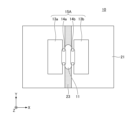
- FIG. 1A and 1B show configuration examples of the optical circuit 10 of the embodiment.
- FIG. 1A is a schematic diagram of the waveguide direction of the optical circuit 10
- FIG. 1B is a top view.
- the plane parallel to the substrate or semiconductor layer 21 is the XY plane
- the normal direction of the substrate or semiconductor layer 21 is the Z direction.
- the optical axis direction of the optical waveguide is the Y direction (either the +Y direction or the ⁇ Y direction).
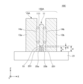
- the optical circuit 10 includes an optical waveguide 23 including a ridge formed on a substrate or semiconductor layer 21 (hereinafter simply referred to as "substrate or the like 21"), and a resonator 11.
- the resonator 11 has an optical circulation surface 111 , and a part of the optical circulation surface 111 is arranged to face the upper surface of the ridge 231 with the first gap 51 interposed therebetween. That is, the optical circuit 10 has the first gap 51 between the resonator 11 and the optical waveguide 23, and the resonator 11 and the optical waveguide 23 are separated.
- a first gap 51 represents the gap at the location where the resonator 11 and the optical waveguide 23 are closest.
- the first gap 51 is the gap at the location where the light circulation surface 111 and the ridge 231 are closest to each other.
- a distance G between a portion of the optical circulation surface 111 and the upper surface of the ridge 231 facing the optical circulation surface 111 is shorter than the distance at which the evanescent wave leaks out.
- the degree of optical coupling between the optical waveguide 23 and the resonator 11 is mainly determined by the wavelength of light, the refractive index of the material, and the distance G between the optical waveguide 23 and the resonator 11.
- the distance G is precisely controlled by the machining accuracy of the optical waveguide 23 and the resonator 11 in the embodiment. This distance G may be about the wavelength of light, and more specifically, it should be shorter than the distance at which the evanescent wave leaks out. Thereby, the optical waveguide 23 and the resonator 11 can be optically coupled.
- a material such as an adhesive that connects a portion of the light circulation surface 111 and the upper surface of the ridge 231 is not interposed in the first gap 51 .
- the optical circuit 10 comprises an optical waveguide 23 including a ridge 231 formed on a substrate or the like 21 and the resonator 11 .
- the resonator 11 is a WGM resonator, and has an optical circulation surface 111 , which is arranged so that a part of the optical circulation surface faces the upper surface of the ridge 231 of the optical waveguide 23 with the first gap 51 interposed therebetween. It is
- the resonator 11 is a WGM resonator capable of confining light along the optical circulation plane 111 . Light is confined in the resonator 11 by circulating while being totally reflected along the optical circulating surface 111 .
- the resonator 11 functions as a high Q value filter in which light of a specific wavelength determined by the circumference of the optical circulation plane 111 and the effective refractive index resonates. By making the light circulation surface 111 a smooth surface, a highly sensitive resonator 11 with small scattering loss can be obtained.
- the surface roughness (Ra) of the optical circulation surface 111 is, for example, 10 nm or less.
- the resonator 11 is held above the optical waveguide 23 via the first gap 51 by the support 15A. Since no material such as an adhesive is interposed between the light circulation surface 111 and the upper surface of the ridge 231, the distance G between the light circulation surface 111 and the upper surface of the ridge 231 is less likely to fluctuate due to temperature changes, vibrations, and the like. . Therefore, the optical waveguide 23 and the resonator 11 can be stably optically coupled.
- the support 15A is fixed to the upper surface of the substrate or the like 21 at a position away from the ridge 231 .
- the support 15A is fixed to the substrate or the like 21 at a position separated from the optical waveguide 23 or the ridge 231 in the XY plane in a direction different from the optical axis of the optical waveguide 23 ( ⁇ X direction in this example). It is
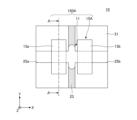
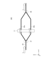
- FIG. 1C is a perspective view of a resonator structure 150A including resonators 11 and supports 15A.
- the support 15A has a first support portion 13a and a second support portion 13b located on both sides of the resonator 11. As shown in FIG.
- the first support portion 13a supports the first surface 11a of the resonator 11 via the first connection portion 14a.
- the second support portion 13b supports the second surface 11b of the resonator 11 opposite to the first surface 11a via the second connection portion 14b.
- the first support portion 13 a and the second support portion 13 b are fixed on the substrate or the like 21 on both sides of the ridge 231 . Thereby, the resonator 11 can be stably supported by the support 15A.
- the maximum length L1 of the first support portion 13a and the second support portion 13b is greater than the maximum length L2 of the resonator 11 in the normal direction of the substrate or the like 21 .
- the first support part 13a and the second support part 13b have a cylindrical shape and are fixed to the substrate or the like 21 at the side surface 131 of the cylinder, but the invention is not limited to this example.
- the first supporting portion 13a and the second supporting portion 13b may be polygonal prisms such as square prisms, hexagonal prisms, and octagonal prisms as long as they can support the resonator 11 .
- the diameter or maximum length L1 of the first support portion 13a and the second support portion 13b is larger than the diameter or maximum length L2 of the resonator 11, and the resonator 11 is placed at a predetermined distance G to guide light. It is held above the wave path 23 .
- the diameter or maximum length L1 of the first support portion 13a and the second support portion 13b may be, for example, 0.05 mm or more and 50 mm or less, preferably 0.05 mm or more and 10 mm or less.
- the diameter or maximum length of the resonator 11 may be 0.999 mm or more and 9.999 mm or less.
- the width of the resonator 11 can be, for example, 1 ⁇ m or more and 100 ⁇ m or less, preferably 10 ⁇ m or more and 50 ⁇ m or less.
- the term "polygonal prism" also includes a state in which processing such as chamfering or chamfering is performed on a part of the prism.
- the substrate or the like 21A is a substrate 211 having an insulating layer 212 .
- Insulating layer 212 is, for example, a silicon oxide film, and optical waveguide 23A including ridge 231 is formed on insulating layer 212 .
- the optical waveguide 23A is made of a material having a higher refractive index than the insulating layer 212. Since the upper surface and both side surfaces of the ridge 231 are surrounded by air, the light is confined inside the ridge 231 and propagates in the Y direction.
- an SOI (Silicon On Insulator) substrate is used as the substrate 21A
- the silicon substrate of the SOI substrate is used as the substrate 211
- the silicon oxide film of the SOI substrate is used as the insulating layer 212
- the silicon layer of the SOI substrate forms the optical waveguide 23A.
- the ridge 231 may be used as the optical waveguide 23A by forming the ridge 231 with a silicon oxide film.
- a silicon waveguide may be used when infrared light is used, and a silicon oxide waveguide may be used when visible light is used.
- the substrate or the like 21B includes a substrate 211 and an n-side semiconductor layer 213 formed on the substrate 211.
- the optical waveguide 23 ⁇ /b>B includes a portion of the n-side semiconductor layer 213 , a p-side semiconductor layer 215 , and an active layer 214 between the n-side semiconductor layer 213 and the p-side semiconductor layer 215 .
- the n-side semiconductor layer 213 includes an n-side cladding layer and an n-side optical guide layer, and includes at least one or more n-type semiconductor layers. A portion protruding from the n-side semiconductor layer 213 becomes the ridge 231 .
- the p-side semiconductor layer 215 includes a p-side optical guide layer and a p-side clad layer, and includes at least one or more p-type semiconductor layers. Also, a p-side contact layer may be further included on the p-side clad layer.
- the active layer 214 may be a multiple quantum well layer comprising multiple barrier layers and well layers.
- the active layer 214 is sandwiched between the n-side cladding layer and the p-side cladding layer having a lower refractive index than the active layer 214 in the stacking direction (Z direction) to confine light.
- the active layer 214 is partitioned by the width of the ridge 231 of the p-side semiconductor layer 215 . Therefore, the region including the active layer 214 determined by the width of the ridge 231 becomes the optical waveguide 23B. That is, the ridge 231 includes part of the n-side semiconductor layer 213 , the active layer 214 and the p-side semiconductor layer 215 .
- a portion of the n-side semiconductor layer 213 included in the ridge 231 preferably includes an n-side cladding layer and an n-side optical guide layer.
- the materials of the n-side semiconductor layer 213, the active layer 214, and the p-side semiconductor layer 215 can be compound semiconductors such as GaN-based semiconductors, InP-based semiconductors, or GaAs-based semiconductors. These materials may be binary, ternary, or quaternary.
- the width of the ridge 231 may be, for example, 0.3 ⁇ m or more and 50 ⁇ m or less.
- the material of substrate 211 may be, for example, sapphire, GaN, GaAs, or the like.
- FIG. 3 is a diagram showing optical coupling between the optical waveguide 23 and the resonator 11.
- the light L indicated by the white arrow propagates through the optical waveguide 23 in the optical axis direction of the optical waveguide 23 (the Y direction in FIG. 3).
- the light L propagates through the optical waveguide 23 while being totally reflected. In the process of this total reflection, the light slightly seeps out from the optical waveguide 23 toward the first gap 51 .
- the light seeping into the gap is called an evanescent wave.
- the distance that the evanescent wave leaks out is about the length of the wavelength.
- the evanescent wave leaking distance is, for example, 700 nm or less, 500 nm or less, 300 nm or less, or 100 nm or less.
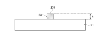
- the resonator 11 is provided above the optical waveguide 23 so as to be positioned at a height of a distance G from the upper surface of the ridge 231 (see FIG. 1A) of the optical waveguide 23 .
- the distance G is shorter than the seepage distance of the evanescent wave. Therefore, the optical waveguide 23 and the resonator 11 are optically coupled, and part of the light L circulates along the optical circulation surface 111 while being totally reflected. Light that circulates while being totally reflected along the light circulation surface 111 seeps slightly from the light circulation surface 111 toward the first gap 51 . Since the resonator 11 and the optical waveguide 23 are optically coupled, part of the light that circulates along the optical circulation surface 111 while being totally reflected propagates through the optical waveguide 23 in the optical axis direction (Y direction).
- An optical sensor which will be described later, can be used as a gyro sensor by detecting the resonance frequency of the resonator 11 from the output light of the optical circuit 10 .
- FIG. 4A is a diagram showing height control of the optical waveguide 23.
- FIG. 4B is a diagram showing processing control of the resonator 11.
- FIG. 4C is a diagram showing the installation of the resonator 11 with respect to the optical waveguide 23.
- the height h of the ridge 231 of the optical waveguide 23 and the height h of the resonator 11 Position control of the optical circulation plane 111 is important.
- the precision of the height h of the ridge 231 of the optical waveguide 23 is determined by the process precision of semiconductor microfabrication.
- the height h of the ridge 231 can be controlled with high precision by forming a thin film as a material of the optical waveguide 23 on the substrate or the like 21 and controlling the amount of etching of the thin film.
- the height h of the ridge 231 can be determined with high precision. You can control it.
- the height h of the ridge 231 is, for example, 300 nm or more and 3000 nm or less, preferably 500 nm or more and 2000 nm or less.
- the optical waveguide 23 may be made of any material as long as it transmits the light to be used and has a higher refractive index than the surrounding medium.
- III-V group compound semiconductors such as GaN-based semiconductors, InP-based semiconductors, and GaAs-based semiconductors may be used.
- the optical waveguide 23 may be made of Si, SiN, SiO 2 , LiNbO 3 or the like.
- the resonator 11 can be integrally formed with the support 15A using a material 140 such as a cylinder or polygonal cylinder.
- material 140 is a cylindrical crystal such as glass, fluoride, oxide, or the like.
- Magnesium fluoride (MgF 2 ), calcium fluoride (CaF 2 ), strontium fluoride (SrF 2 ), yttrium lithium fluoride (LiYF 4 ), and the like can be used as fluoride crystals. These materials have high transmittance for a wide range of wavelengths from visible light to infrared light, and hardly absorb light.
- As the glass general optical glass such as BK-7 (borosilicate crown glass) can be used.
- Crystals of LiNbO 3 , LiTaO 3 , LiCaO 3 , BaTiO 3 , Al 2 O 3 , Ga 2 O 3 , Y 2 O 3 , Y 3 Al 5 O 12 , Lu 3 Al 5 O 12 , ScAlMgO 4 as oxides can be used.
- Material 140 is preferably MgF2 , CaF2 , LiNbO3 . These materials have high transmittance and birefringence, and are excellent as resonator materials.
- the machining of the resonator 11 is performed, for example, by pressing a diamond knife against the side surface 131 of the cylinder while rotating the cylinder-shaped material 140 with a diameter L1 around the central axis.
- the resonator 11 having the optical circulation plane 111 can be processed with high accuracy.
- a digging amount d up to the optical circulation plane 111 is, for example, 400 nm or more and 3100 nm or less, preferably 600 nm or more and 2100 nm or less.
- the remaining portions of the material 140 that are not scraped off become the first support portion 13a and the second support portion 13b of the support 15A.
- a resonator structure 150A in which the resonator 11 and the support 15A are integrally formed is obtained, and the resonator 11 can be more stably supported by the substrate 21 or the like.
- the side surfaces 131 of the cylinders of the first support portion 13a and the second support portion 13b are fixed surfaces to the substrate or the like 21, as will be described later.
- a first connection portion 14a formed between the resonator 11 and the first support portion 13a by machining is also formed integrally with the resonator 11 and the first support portion 13a.
- a second connection portion 14b formed between the resonator 11 and the second support portion 13b by machining is also formed integrally with the resonator 11 and the second support portion 13b.
- the width of the first connection portion 14 a that is, the distance between the resonator 11 and the first support portion 13 a is longer than the wavelength of the light circulating inside the resonator 11 .
- first connection portion 14a and the second connection portion 14b By forming the first connection portion 14a and the second connection portion 14b, the distance between the light circulation surface 111 and the side surface of the first support portion 13a on the resonator 11 side and between the light circulation surface 111 and the second support portion 13b is increased. A gap is formed between the side surface of the resonator 11 and light can be efficiently confined within the resonator 11 .
- the resonator structure 150A is fixed to the substrate or the like 21 so that the optical circulation surface 111 of the resonator 11 corresponds to the upper surface of the optical waveguide 23.
- the height h of the ridge 231 of the optical waveguide 23 and the depth d of the recess from the side surface 131 of the material 140 are precisely controlled.
- the distance G between the upper surface of the ridge 231 and the optical circulation surface 111 is determined in a self-aligning manner at the stage of assembly. For example, when the digging depth d is 1100 nm and the height h is 1000 nm, the distance G is approximately 100 nm.
- a first gap 51 (see FIG. 1A) is provided between the resonator 11 and the optical waveguide 23, and since no material such as adhesive is interposed therebetween, the gap is highly stable against temperature changes, vibrations, and the like.
- FIG. 5 is a schematic plan view showing a configuration example of an optical circuit 10A in which a resonator structure 150A is arranged
- FIG. 6 is a schematic diagram of an optical sensor 100A to which the optical circuit 10A is applied.
- the optical circuit 10A has a light source 31, an optical waveguide 23, a resonator structure 150A including a resonator 11, a first output waveguide 24a, and a second output waveguide 24b.
- the optical sensor 100A includes an optical circuit 10A, photodetectors PD1 and PD2 that detect light circulating in the resonator 11, and a processor that processes the outputs of the photodetectors.
- Optical sensor 100 is, for example, a gyro sensor.
- the light source 31 is, for example, a ring laser formed of a ring waveguide 311 provided on the substrate 21 or the like.
- the ring waveguide 311 can be formed of the optical waveguide described with reference to FIG. 2B.
- Light source 31 outputs light having a peak wavelength of, for example, 200 nm or more and 1600 nm or less. Further, the light source 31 may output light having a peak wavelength of 200 nm or more and 550 nm or less, for example. By using light with a relatively short wavelength, it is possible to increase the phase change associated with the Sagnac effect and improve the sensitivity of the sensor. Further, the light source 31 may output light having a peak wavelength of 630 nm or more and 1560 nm or less, for example.
- the distance for optically coupling the light source 31 and the optical waveguide 23 and the distance for optically coupling the optical waveguide 23 and the resonator 11 can be increased. This facilitates fabrication of the optical circuit 10A and the optical sensor 100A. Also, the optical Kerr effect of the resonator 11, which will be described later, can be reduced.
- Light source 31 preferably outputs light of a single wavelength. Thereby, the noise of the optical sensor can be reduced.
- the ring waveguide 311 is preferably a waveguide that satisfies a single mode condition. Since the transverse mode is the fundamental mode, it is easy to control the light propagating through the optical waveguide 23 .
- the width of the ring waveguide 311 can be, for example, 0.3 ⁇ m or more and 2 ⁇ m or less.
- the optical waveguide 23 may be a waveguide having the same configuration as the ring waveguide 311, or may be a thin wire waveguide such as SiO 2 described with reference to FIG. 2A.
- the optical waveguide 23 and the ring waveguide 311 of the light source 31 are preferably made of the same Group III-V compound semiconductor.
- a substrate or the like 21B including a substrate 211, an n-side semiconductor layer 213, an active layer 214, and a p-side semiconductor layer 215 in order using photolithography and/or electron beam lithography or the like, the light can be guided.
- a ring waveguide 311 of the waveguide 23 and the light source 31 can be formed.
- the optical waveguide 23 and the ring waveguide 311 of the light source 31 are formed by removing the substrate or the like 21B from the p-side semiconductor layer 215 to part of the n-side semiconductor layer 213 by photolithography and/or electron beam lithography. can be done. It does not require an external light source because it emits light upon application of III-V compound semiconductor current. Thereby, the optical circuit 10A can be miniaturized. Moreover, the magnitude of optical coupling between the light source 31 and the optical waveguide 23 can be stabilized.
- the optical waveguide 23 has an optical coupler 32 with a branching ratio of 50:50.
- the optical coupler 32 is formed by part of the optical waveguide 23 and another part of the optical waveguide 23 .
- a loop 35 includes a portion of the optical waveguide 23 optically coupled by the optical coupler 32, another portion of the optical waveguide 23, and the optical waveguide 23 existing therebetween.
- Light output from the light source 31 is branched by the optical coupler 32 at an intensity ratio of 50:50.
- Optical coupler 32 may be, for example, a directional coupler or a Y-waveguide. One branched light passes counterclockwise through the loop 35 and circulates around the resonator 11 counterclockwise.
- the other light passes clockwise through loop 35 and circulates around resonator 11 clockwise.
- the optical path length sensed by the light circulating in the resonator 11 changes depending on the rotation angle or angular velocity of the substrate or the like 21 .
- the resonance frequency of the resonator 11 for light circulating clockwise and the resonance frequency of the resonator 11 for light circulating counterclockwise change (Sagnac effect).
- the angular velocity can be calculated from the difference between the resonance frequency of the resonator 11 for the clockwise circulating light and the resonance frequency of the resonator 11 for the counterclockwise circulating light.
- the optical circuit 10A has optical couplers 33 and 34 in the middle of the loop 35 .
- the optical coupler 33 is formed by part of the optical waveguide 23 and part of the first output waveguide 24a.
- the optical coupler 34 is formed by part of the optical waveguide 23 and part of the second output waveguide 24b. As shown in FIG. They are arranged on one side and the other side of the loop 35 through the body 150A.
- Optical couplers 33 and 34 may have a splitting ratio of 50:50, for example, and may be directional couplers.
- Part of the light that has circulated clockwise around the resonator 11 is guided to the first output waveguide 24a by the optical coupler 33 and detected by the first photodetector (denoted as "PD1" in the figure). be done.
- a part of the light circulating counterclockwise in the resonator 11 is guided to the second output waveguide 24b by the optical coupler 34, and is detected by the second photodetector (denoted as "PD2
- the intensity of light detected by the first photodetector (PD1) is measured by the lock-in amplifier 41.
- a measurement result obtained by the lock-in amplifier 41 is fed back to the light source 31 via the control circuit 42 and input to the processor 50A.
- the wavelength of light source 31 is controlled based on feedback from control circuit 42 .
- the control circuit 42 can use, for example, a PID (Proportional-Integral-Differential) control circuit.
- the intensity of light detected by the second photodetector (PD2) is measured by the lock-in amplifier 43.
- a measurement result obtained by the lock-in amplifier 43 is input to the processor 50A.
- Processor 50A processes the input signal. Specifically, the processor 50A outputs the output of the lock-in amplifier 41, that is, the detection result of the first photodetector (PD1), and the output of the lock-in amplifier 43, that is, the detection result of the second photodetector (PD2).
- Angular velocity is calculated from the difference from the result and output. This means, for example, measuring the amount of deviation of the detected amount of PD2 based on the detected amount of PD1. From this difference, the angular velocity received by the optical sensor 100A can be obtained and output.
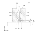
- FIG. 7 and 8 are diagrams showing fixing of the resonator structure 150A to the substrate or the like 21.
- FIG. 7 is a top view
- FIG. 8 is a sectional view taken along line AA' of FIG.
- FIG. 8 is a vertical cross section of the first supporting portion 13a seen in the optical axis direction (X direction) of the optical waveguide 23.
- a vertical cross section of the second supporting portion 13b seen in the -X direction is also It is the same as the vertical section of 13a.
- the first support portion 13a and the second support portion 13b are cylindrical.
- a first groove 25a and a second groove 25b are formed in the substrate or the like 21 so as to extend in directions different from the optical axis of the ridge 231 (see FIG. 1A) of the optical waveguide 23 (for example, ⁇ X directions).
- the widths of the first groove 25a and the second groove 25b in the optical axis direction of the optical waveguide 23 formed between the first groove 25a and the second groove 25b are the first support portion 13a and the second support portion 13b. , may be 0.8 times or less, may be 0.6 times or less, or may be 0.4 times or less. As shown in FIG.
- the side surface 131 of the first support portion 13a of the support 15A is in contact with the edges 252 and 253 of the upper end of the first groove 25a.
- a second gap 52 is provided between the bottom surface of the first groove 25a and the first support portion 13a.
- the first support portion 13a does not contact the substrate or the like 21 or the first groove 25a at locations other than P1 and P2.
- the second gap 52 is provided between the side surface 131 of the first support portion 13a and the bottom surface 251 of the first groove 25a.
- a third gap 53 is provided between the first connection portion 14 a and the substrate or the like 21 . Even if the first groove 25a is provided, the distance G is maintained so that the optical waveguide 23 and the resonator 11 are optically coupled.
- the second support portion 13b of the support 15A also has the same positional relationship as the first support portion 13a with respect to the substrate or the like 21 and the second groove 25b. That is, the side surface 131 of the second support portion 13b contacts the edges 252 and 253 of the second groove 25b at the upper end of the second groove 25b.
- a second gap 52 is provided between the side surface 131 of the second support portion 13b and the bottom surface 251 of the second groove 25b, and a third gap 53 is provided between the second connection portion 14b and the substrate 21 or the like.
- the first groove 25a and the second groove 25b may be referred to as the "groove 25" without distinction.
- the first gap 51 is between the resonator 11 and the optical waveguide 23
- the second gap 52 is between the resonator structure 150A and the first groove 25a
- the first connecting portion 14a and the substrate 21, etc. is the third gap 53 .
- the resonator structure 150A is supported by the upper edges 252 and 253 of the first groove 25a with the resonator 11 floating above the optical waveguide .
- the resonator structure 150A is in contact with the substrate or the like 21 only at two points P1 and P2. As a result, the entire resonator structure 150A is less susceptible to temperature changes and vibrations.
- the distance G between the upper surface of the ridge 231 and the optical circulation surface 111 can be stabilized.
- the distance G is equal to or less than the vacuum wavelength of light propagating through the optical waveguide 23 .
- the distance G may be, for example, 700 nm or less, 500 nm or less, 300 nm or less, 100 nm or less, 90 nm or less, 80 nm or less, or 70 nm or less. may be
- FIG. 9 shows an example of a fixing method for the resonator structure 150A.
- the substrate or the like 21 on which the resonator structure 150A is mounted may be sandwiched between the plates 61 and 62 from above and below.
- Plates 61 and 62 may be made of brass, copper, for example.
- the plates 61 and 62 may be dielectric substrates having a small difference in thermal expansion coefficient from the substrate or the like 21 and/or the resonator structure 150A. As a result, separation between the substrate or the like 21 and the plate 61 or separation between the resonator structure 150A and the plate 62 due to temperature changes can be reduced, and the resonator structure 150A can be fixed.
- a part of the resonator structure 150A may be temporarily fixed to the substrate or the like 21 in a region other than the groove 25 and the optical waveguide 23 prior to clamping with the screws 43, 44, clamps, or the like.
- the distance between the resonator 11 and the optical waveguide 23 is kept constant, and the optical coupling can be stabilized.
- the resonator 11 having the optical circulation plane 111 When the resonator 11 having the optical circulation plane 111 is used, the light circulates many times along the optical circulation plane 111, so that the intensity of the light constructive by interference increases. High light intensity results in the optical Kerr effect, in which the refractive index changes with light intensity. The change in the optical path length of the resonator 11 due to the optical Kerr effect cannot be distinguished from the difference in the optical path length of the gyro sensor due to the angular velocity, resulting in noise. Therefore, considering the optical Kerr effect, it is difficult to increase the optical power, and sensitivity may be limited.
- high-order modes (hereinafter also referred to as "high-order modes") among the transverse modes of the resonator.
- the electric field intensity distribution of the higher-order mode has more antinodes and nodes than the electric field intensity distribution of the fundamental mode, and is widely distributed. Therefore, by utilizing this higher-order mode, in the resonator 11, the intensity per unit area of light coupled to the resonator 11 can be reduced. As a result, noise due to the optical Kerr effect can be reduced and sensitivity can be improved while increasing the intensity of the light amplified within the resonator 11 .
- FIG. 10 is a schematic diagram of the waveguide direction of an optical circuit 10C using higher-order modes.
- An optical waveguide including two or more ridges is used to selectively utilize higher-order modes.
- Optical waveguides 23a and 23b each including a ridge 231 are arranged in parallel on a substrate 21 or the like.
- the optical waveguides 23 a and 23 b are arranged so that the upper surface of the ridge 231 faces the position where the higher-order mode occurs on the optical circulation plane 111 of the resonator 11 .
- the high-order mode of the resonator 11 and the transverse modes of the optical waveguides 23a and 23b can be efficiently coupled.
- the optical waveguides 23a and 23b each satisfy a single mode condition. Since the electric field intensity distribution of the fundamental mode is unimodal, it is easy to optically couple with higher-order modes of the resonator 11 having a plurality of antinodes in the electric field intensity distribution.
- the widths of the optical waveguides 23a and 23b that satisfy the single mode condition can be, for example, 0.3 ⁇ m or more and 5 ⁇ m or less.
- the ring waveguide 311 of the light source 31 preferably satisfies a single mode condition. That is, the transverse mode of light generated by the light source 31 is preferably the fundamental mode.
- the distance G between the upper surface of the ridge 231 of the optical waveguides 23a, 23b and the resonator 11 is precisely controlled by the processing accuracy of the optical waveguides 23a, 23b and the processing accuracy of the resonator structure 150A.
- the structure of the resonator structure 150A is the same as that in FIG. 1A, and the same components are denoted by the same reference numerals, and overlapping descriptions are omitted.
- FIG. 11A is a schematic plan view of the optical circuit 10C.
- the optical waveguide 23 includes a first mode converter 37 that divides the ridge 231 into a plurality of ridges and a second mode converter 38 that connects the plurality of ridges into one ridge.
- FIG. 11A exemplifies the case of being divided into two ridges.
- a portion of the optical circulation plane 111 of the resonator 11 faces a plurality of ridges separated by the first mode converter 37 via the first gaps 51 .
- a first mode converter 37 converts the modes and a second mode converter 38 combines the converted modes.
- the first mode converter 37 and the second mode converter 38 may be realized by a Y-shaped waveguide that branches one waveguide into two, or an optical coupler with a branch ratio of 50:50, multimode interference ( An MMI (Multi-Mode Interference) coupler or the like may be used.
- MMI Multi-Mode Interference
- the two lights that have been mode-converted propagate through the optical waveguides 23a and 23b, respectively, and are optically coupled at the position where the higher-order mode of the resonator 11 is generated.
- the two transverse modes of light coupled to the resonator 11 are distributed over a wide area on the optical circulation plane 111, and the intensity per unit area can be reduced. Noise due to effects can be reduced.
- the two optical waveguides 23a and 23b preferably have optical path lengths designed to be phase-matched.
- FIG. 11B is a modification of the schematic plan view of the optical circuit 10C. Only points different from FIG. 11A will be described.
- the optical waveguides 23a and 23b form a tapered waveguide.
- the optical waveguide 23a includes two narrow portions 235a, two tapered portions 236a, and a wide portion 237a. Two tapered portions 236a and a wide portion 237a are provided between the two narrow portions 235a. Also, the wide portion 237a is provided between the two tapered portions 236a.
- the waveguide width of the wide portion 237a may be greater than the waveguide width of the narrow portion 235a, and may be, for example, 2 times or more and 35 times or less.
- the waveguide width of the narrow portion 235a may be, for example, 0.3 ⁇ m or more and 5 ⁇ m or less.
- the waveguide width of the wide portion 237a is larger than the waveguide width of the narrow portion 235a, and may be, for example, 1 ⁇ m or more and 10 ⁇ m or less.
- Each tapered portion 236a is formed such that the waveguide width increases from the narrow portion 235a to the wide portion 237a.
- the optical waveguide 23a and the resonator 11 face each other at the wide portion 237a.
- the optical waveguide 23b includes two narrow portions 235b, two tapered portions 236b, and a wide portion 237b. Other configurations are the same as those of the optical waveguide 23a forming a tapered waveguide.
- the number of ridges 231 including the optical waveguide 23 may be increased according to the order of the transverse mode of the resonator 11 .
- each optical waveguide 23 facing the resonator 11 can be formed to satisfy single mode conditions.
- the optical waveguide 23 may be divided into four using a 1:4 MMI coupler or the like.
- at least two of the plurality of ridges 231 are preferably opposed to positions where high-order transverse modes of the resonator 11 occur.
- FIG. 12 shows a configuration example of an optical circuit 10B using a resonator structure 150B.
- FIG. 13 is a schematic diagram of an optical sensor using the optical circuit 10B.
- Optical sensor 100B is, for example, an acceleration sensor.
- a resonator structure 150B used in the optical circuit 10B includes a resonator 11 having an optical circulation plane 111 and a support 15B.
- the support 15B has a support portion 13c that supports only one of the first surface 11a and the second surface 11b of the resonator 11. As shown in FIG. In this example, the support portion 13c is connected to the first surface 11a of the resonator 11 by the connection portion 14c.
- the resonator structure 150B can be manufactured by controlling the rotational speed of the material 140 and the pressing force of the diamond knife for precision machining.
- the resonator 11 is supported by the supporting portion 13c via the connecting portion 14c such that the optical circulation surface 111 thereof faces the upper surface of the ridge 231 of the optical waveguide 23 .
- the support portion 13c has, for example, a cylindrical shape.
- the support portion 13c is supported at two points P1 and P2 by the edges 252 and 253 of the upper end of the groove 25 formed in the substrate or the like 21. .
- a cylindrical support portion 13 c is supported by the groove 25 .
- Groove 25 extends in a direction different from the optical axis of optical waveguide 23 or ridge 231 (eg, away from the optical axis).
- the side surface of the support portion 13c contacts with the groove edges 252 and 253 at the upper end of the groove 25, and a second gap 52 (see FIG. 8) is formed between the support portion 13c and the bottom surface of the groove 25, and the substrate 21, etc. and the support portion 13c, a third gap 53 (see FIG.
- the optical circuit 10B is less likely to be affected by temperature changes and vibrations, so it is possible to suppress changes in light response due to factors other than acceleration.
- the fixation of the resonator structure 150B to the edges 252, 253 of the groove 25 may be reinforced by screws, clamps or the like.
- the resonator 11 which has a smaller mass than the supporting portion 13c, is held like a cantilever by the elongated connecting portion 14c. That is, it has a structure in which one end of the resonator 11 is fixed to the support 15B and the other end on the opposite side is free.
- the maximum length of the connecting portion 14 c is smaller than the maximum length of the resonator 11 in the normal direction of the substrate or the like 21 .
- the distance between the support portion 13c and the resonator 11 is greater than the maximum length of the connecting portion.
- the distance G between the optical circulation plane of the resonator 11 and the upper surface of the ridge 231 is set to a predetermined design value by controlling the height of the optical waveguide 23 and the depth of the material 140. be done.
- the optical circuit 10B is applied to an acceleration sensor, the inertial force due to acceleration changes the distance G.
- the optical sensor 100B can measure acceleration by reading changes in the distance G as changes in the intensity of light.
- the optical circuit 10B has a light source 31, an optical waveguide 23, and a resonator structure 150B including the resonator 11.
- the light source 31 is a single-wavelength laser light source formed of, for example, a ring waveguide 311 .
- the ring waveguide 311 and the optical waveguide 23 are optically coupled, and the optical waveguide 23 and the resonator 11 are optically coupled. That is, the distance between the ring waveguide 311 and the optical waveguide 23 is shorter than the distance through which the evanescent wave seeps out, and the distance between the optical waveguide 23 and the resonator 11 is also shorter than the distance through which the evanescent wave seeps out. .
- Light output from the light source 31 propagates through the optical waveguide 23 , and the light propagated through the optical waveguide 23 circulates along the optical circulation plane 111 of the resonator 11 .
- the circulated light propagates through the optical waveguide 23 and is detected by the photodetector (PD3).
- the intensity of light received by the photodetector (PD3) changes according to the distance G between the optical circuit plane 111 of the resonator 11 and the optical waveguide 23, that is, the acceleration received by the optical sensor 100B.
- the intensity of light detected by the photodetector (PD3) is measured by the lock-in amplifier 44 and input to the processor 50B.
- Processor 50B calculates and outputs the acceleration from the detected light intensity changes.
- the distance G between the upper surface of the optical waveguide 23 and the optical circulation surface 111 is precisely set without being accelerated, and the resonator structure 150B is stably attached to the substrate or the like 21. Fixed.
- the resonator 11 is accelerated, only one of the first surface 11a and the second surface 11b of the resonator 11 is supported by the support portion 13c. Therefore, the inertial force caused by the acceleration causes the resonator 11 to move, and the acceleration can be accurately measured. can do.
- the ridge of the optical waveguide 23 of the optical circuit 10B is divided into a plurality of ridges, and the optical circulation plane of the resonator 11 is divided into a plurality of ridges with a first gap 51 (see FIG. 10) therebetween. It may be configured to face the .
- a first mode converter 37 that divides the optical waveguide 23 into a plurality of ridges and a second mode converter 38 that connects the plurality of ridges into one ridge may be provided. good.
- At least two of the plurality of ridges 231 preferably face positions where high-order transverse modes of the resonator 11 occur.
- information terminals such as smartphones, tablet terminals, and watches, and mobile objects such as drones, vehicles, ships, and aircraft can be equipped with optical circuits 10A and 10B or optical sensors 100A and 100B of the present disclosure.
- a gyro sensor as an optical sensor
- the inclination of the body can be controlled.
- an acceleration sensor as an optical sensor
- the movement speed can be controlled.
- a vehicle equipped with a gyro sensor and/or an acceleration sensor as an optical sensor can form part of a driving assistance system.
- optical circuits 10A and 10B or the optical sensors 100A and 100B according to the present disclosure can be used, for example, in driving support systems for mobile bodies. Since the optical sensors 100A and 100B according to the present disclosure have few moving parts, they have high robustness and can be suitably used for mobile objects that require safety.
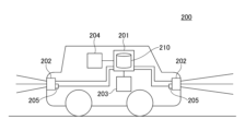
- FIG. 14 is a schematic diagram of a driving support system mounted on a mobile object 200 such as a vehicle.
- the driving support system shown in FIG. 14 is mounted on a vehicle and includes an on-vehicle device 201 that performs control related to driving support of the vehicle, a LiDAR 202, a gyro sensor 203, a vehicle body acceleration sensor 204, and a LiDAR acceleration sensor 205. .
- the in-vehicle device 201 is electrically connected to the LiDAR 202, the gyro sensor 203, the vehicle body acceleration sensor 204, and the LiDAR acceleration sensor 205, and acquires their output data. It also stores a map database (DB: DataBase) 210 that stores road data and feature information about features provided near roads.
- DB DataBase
- the in-vehicle device 201 estimates the position of the vehicle based on the output data and the map DB 210 described above, and performs control related to vehicle driving support such as automatic driving control based on the estimation result of the own vehicle position.
- the vehicle-mounted device 201 estimates the attitude and position of the LiDAR 202 based on outputs from the LiDAR 202 , the gyro sensor 203 , the vehicle body acceleration sensor 204 , and the LiDAR acceleration sensor 205 . Based on this estimation result, the vehicle-mounted device 201 performs processing such as correcting each measurement value of the point cloud data output by the LiDAR 202 .
- the LiDAR 202 discretely measures the distance to an object in the external world by emitting a pulsed laser over a predetermined angular range in the horizontal and vertical directions, and creates a three-dimensional point cloud indicating the position of the object. Generate information.
- the LiDAR 202 includes an irradiation unit that irradiates laser light while changing the irradiation direction, a light receiving unit that receives reflected light or scattered light of the irradiated laser light, and scan data based on the light receiving signal output by the light receiving unit.
- the scan data is generated based on the irradiation direction corresponding to the laser beam received by the light receiving unit and the distance to the object in the irradiation direction of the laser beam specified based on the above-described light reception signal.
- the LiDARs 202 are provided at the front and rear portions of the vehicle.
- the gyro sensor 203 is installed in the vehicle and supplies an output signal corresponding to the yaw rate of the vehicle body to the vehicle-mounted device 201 .
- the gyro sensor 203 is the optical sensor 100A described in the embodiment according to the present disclosure.
- a plurality of gyro sensors 203 may be provided.
- the gyro sensors 203 may be provided on the front wheel side and the rear wheel side of the vehicle, respectively, and each gyro sensor 203 may be electrically connected to the vehicle-mounted device 201 .
- the traveling direction of the vehicle can be controlled more precisely.
- the vehicle body acceleration sensor 204 is an acceleration sensor provided in the vehicle, and supplies detection signals corresponding to 3-axis acceleration data corresponding to the traveling direction, side direction, and height direction of the vehicle body to the in-vehicle device 201 .
- the LiDAR acceleration sensor 205 is a three-axis acceleration sensor provided in each LiDAR 202 and supplies detection signals corresponding to three-axis acceleration data of the installed LiDAR 202 to the in-vehicle device 201 .
- the vehicle body acceleration sensor 204 and the LiDAR acceleration sensor 205 are the optical sensor 100B described in the embodiment according to the present disclosure. Three-axis acceleration data can be obtained by providing optical sensors 100B in each axis direction.
- Electrodes are provided in the vicinity of the optical waveguide 23, the optical couplers 32, 33, and 34, or the first mode converter 37 and the second mode converter 38, which constitute the optical circuit 10, and the phase and mode of light are branched by applying a voltage.
- the ratio, etc. may be fine-tuned.
- the electrodes may be formed of a good conductor with high adhesion to the base.
- the light source 31 outputs light of a single wavelength and couples the light of the single wavelength to the resonator 11, but the present invention is not limited to this example.
- Light including multiple wavelengths, such as a WDM signal may be wavelength-separated and optically coupled to the resonator.
- Reference Signs List 10 10A, 10B, 10C
- Optical circuit 11 Resonator 11a First surface 11b Second surface 111
- Support 21 Substrate or semiconductor layer 23, 23a, 23b
Landscapes
- Physics & Mathematics (AREA)
- General Physics & Mathematics (AREA)
- Optics & Photonics (AREA)
- Engineering & Computer Science (AREA)
- Microelectronics & Electronic Packaging (AREA)
- Optical Integrated Circuits (AREA)
Priority Applications (4)
| Application Number | Priority Date | Filing Date | Title |
|---|---|---|---|
| JP2023564921A JPWO2023100742A1 (https=) | 2021-11-30 | 2022-11-24 | |
| EP22901175.4A EP4443206A4 (en) | 2021-11-30 | 2022-11-24 | OPTICAL CIRCUIT, OPTICAL SENSOR USING SAME AND MOVING BODY |
| CN202280078978.2A CN118339490A (zh) | 2021-11-30 | 2022-11-24 | 光电路、使用该光电路的光传感器和移动体 |
| US18/714,074 US20250035842A1 (en) | 2021-11-30 | 2022-11-24 | Optical circuit, optical sensor, and mobile body using the optical circuit |
Applications Claiming Priority (2)
| Application Number | Priority Date | Filing Date | Title |
|---|---|---|---|
| JP2021-194775 | 2021-11-30 | ||
| JP2021194775 | 2021-11-30 |
Publications (1)
| Publication Number | Publication Date |
|---|---|
| WO2023100742A1 true WO2023100742A1 (ja) | 2023-06-08 |
Family
ID=86612107
Family Applications (1)
| Application Number | Title | Priority Date | Filing Date |
|---|---|---|---|
| PCT/JP2022/043379 Ceased WO2023100742A1 (ja) | 2021-11-30 | 2022-11-24 | 光回路、これを用いた光センサ、及び移動体 |
Country Status (5)
| Country | Link |
|---|---|
| US (1) | US20250035842A1 (https=) |
| EP (1) | EP4443206A4 (https=) |
| JP (1) | JPWO2023100742A1 (https=) |
| CN (1) | CN118339490A (https=) |
| WO (1) | WO2023100742A1 (https=) |
Citations (7)
| Publication number | Priority date | Publication date | Assignee | Title |
|---|---|---|---|---|
| US20030206693A1 (en) * | 2001-06-28 | 2003-11-06 | Tapalian Haig Charles | Optical microcavity resonator sensor |
| JP2007508714A (ja) * | 2003-10-14 | 2007-04-05 | スリーエム イノベイティブ プロパティズ カンパニー | ハイブリッド球−導波路共振器 |
| US7283707B1 (en) * | 2001-07-25 | 2007-10-16 | Oewaves, Inc. | Evanescently coupling light between waveguides and whispering-gallery mode optical resonators |
| JP2008516285A (ja) * | 2004-10-06 | 2008-05-15 | コーニング インコーポレイテッド | 横断方向閉ループ共振器 |
| WO2019012245A1 (en) * | 2017-07-11 | 2019-01-17 | Ucl Business Plc | ECHO GALLERY INERTIAL SENSOR AND METHOD THEREOF |
| US20200400888A1 (en) | 2019-06-04 | 2020-12-24 | Gm Cruise Holdings Llc | Systems and methods for efficient coupling between integrated photonic waveguides and electro-optic resonator |
| JP2021194775A (ja) | 2020-06-09 | 2021-12-27 | 京セラドキュメントソリューションズ株式会社 | 画像形成装置 |
Family Cites Families (1)
| Publication number | Priority date | Publication date | Assignee | Title |
|---|---|---|---|---|
| US7389025B2 (en) * | 2006-03-29 | 2008-06-17 | 3M Innovative Properties Company | Coupling light into microresonators |
-
2022
- 2022-11-24 JP JP2023564921A patent/JPWO2023100742A1/ja active Pending
- 2022-11-24 CN CN202280078978.2A patent/CN118339490A/zh active Pending
- 2022-11-24 WO PCT/JP2022/043379 patent/WO2023100742A1/ja not_active Ceased
- 2022-11-24 EP EP22901175.4A patent/EP4443206A4/en active Pending
- 2022-11-24 US US18/714,074 patent/US20250035842A1/en active Pending
Patent Citations (7)
| Publication number | Priority date | Publication date | Assignee | Title |
|---|---|---|---|---|
| US20030206693A1 (en) * | 2001-06-28 | 2003-11-06 | Tapalian Haig Charles | Optical microcavity resonator sensor |
| US7283707B1 (en) * | 2001-07-25 | 2007-10-16 | Oewaves, Inc. | Evanescently coupling light between waveguides and whispering-gallery mode optical resonators |
| JP2007508714A (ja) * | 2003-10-14 | 2007-04-05 | スリーエム イノベイティブ プロパティズ カンパニー | ハイブリッド球−導波路共振器 |
| JP2008516285A (ja) * | 2004-10-06 | 2008-05-15 | コーニング インコーポレイテッド | 横断方向閉ループ共振器 |
| WO2019012245A1 (en) * | 2017-07-11 | 2019-01-17 | Ucl Business Plc | ECHO GALLERY INERTIAL SENSOR AND METHOD THEREOF |
| US20200400888A1 (en) | 2019-06-04 | 2020-12-24 | Gm Cruise Holdings Llc | Systems and methods for efficient coupling between integrated photonic waveguides and electro-optic resonator |
| JP2021194775A (ja) | 2020-06-09 | 2021-12-27 | 京セラドキュメントソリューションズ株式会社 | 画像形成装置 |
Non-Patent Citations (1)
| Title |
|---|
| See also references of EP4443206A4 |
Also Published As
| Publication number | Publication date |
|---|---|
| EP4443206A1 (en) | 2024-10-09 |
| US20250035842A1 (en) | 2025-01-30 |
| EP4443206A4 (en) | 2025-10-15 |
| CN118339490A (zh) | 2024-07-12 |
| JPWO2023100742A1 (https=) | 2023-06-08 |
Similar Documents
| Publication | Publication Date | Title |
|---|---|---|
| US8744222B2 (en) | Practical silicon photonic multi-function integrated-optic chip for fiber sensor applications | |
| Dell’Olio et al. | Recent advances in miniaturized optical gyroscopes | |
| JP5474282B2 (ja) | 集積光学回転センサおよび回転レートを検出する方法 | |
| US20190101392A1 (en) | Multilayer waveguide optical gyroscope | |
| CA2034899C (en) | Integrated optics decorrelator | |
| JP2020510199A (ja) | 干渉型光ファイバ・ジャイロスコープ(ifog)用の光集積回路 | |
| EP0483993A2 (en) | Integrated optics gyroscope sensor | |
| JP2001242327A (ja) | 改良された偏光消光比を有する多機能一体化光学チップ | |
| EP1939636A1 (en) | Fiber optic current sensor and method for sensing current using same | |
| US20080024786A1 (en) | Fiber optic gyroscope having a silicon-based optical chip | |
| US7228022B1 (en) | Polymer integrated optical transceiver | |
| US20250306269A1 (en) | Method for fabricating an optical waveguide structure | |
| JP2009150886A (ja) | 光ファイバ電流センサおよびそれを用いた電流検知方法 | |
| WO2023100742A1 (ja) | 光回路、これを用いた光センサ、及び移動体 | |
| EP4455608A1 (en) | Optical circuit, and optical circuit device, sensor, and moving body employing same | |
| US20090142015A1 (en) | Optical modulators | |
| US20210011216A1 (en) | Optical modulator and optical measurement apparatus | |
| US11381056B2 (en) | Laser cavity construction for reduced wavelengths | |
| EP1219926B1 (en) | Integrated optical angular velocity sensor | |
| US7239765B1 (en) | Polymer phase modulator | |
| US12105327B2 (en) | Resonator with at least two cores and gyroscope applications thereof | |
| JP2008002954A (ja) | 光ジャイロ | |
| CA2417113A1 (en) | Integrated optic gyroscope and method of fabrication | |
| JPS5966181A (ja) | 集積型半導体レ−ザジヤイロ | |
| JPH03142317A (ja) | 光ジャイロ |
Legal Events
| Date | Code | Title | Description |
|---|---|---|---|
| 121 | Ep: the epo has been informed by wipo that ep was designated in this application |
Ref document number: 22901175 Country of ref document: EP Kind code of ref document: A1 |
|
| WWE | Wipo information: entry into national phase |
Ref document number: 18714074 Country of ref document: US |
|
| ENP | Entry into the national phase |
Ref document number: 2023564921 Country of ref document: JP Kind code of ref document: A |
|
| WWE | Wipo information: entry into national phase |
Ref document number: 202280078978.2 Country of ref document: CN |
|
| NENP | Non-entry into the national phase |
Ref country code: DE |
|
| ENP | Entry into the national phase |
Ref document number: 2022901175 Country of ref document: EP Effective date: 20240701 |