WO2023100019A1 - 有機化合物、有機デバイス、発光装置および電子機器 - Google Patents
有機化合物、有機デバイス、発光装置および電子機器 Download PDFInfo
- Publication number
- WO2023100019A1 WO2023100019A1 PCT/IB2022/061119 IB2022061119W WO2023100019A1 WO 2023100019 A1 WO2023100019 A1 WO 2023100019A1 IB 2022061119 W IB2022061119 W IB 2022061119W WO 2023100019 A1 WO2023100019 A1 WO 2023100019A1
- Authority
- WO
- WIPO (PCT)
- Prior art keywords
- light
- layer
- abbreviation
- phenyl
- substituted
- Prior art date
- Legal status (The legal status is an assumption and is not a legal conclusion. Google has not performed a legal analysis and makes no representation as to the accuracy of the status listed.)
- Ceased
Links
Images

























Classifications
-
- C—CHEMISTRY; METALLURGY
- C07—ORGANIC CHEMISTRY
- C07D—HETEROCYCLIC COMPOUNDS
- C07D403/00—Heterocyclic compounds containing two or more hetero rings, having nitrogen atoms as the only ring hetero atoms, not provided for by group C07D401/00
- C07D403/02—Heterocyclic compounds containing two or more hetero rings, having nitrogen atoms as the only ring hetero atoms, not provided for by group C07D401/00 containing two hetero rings
- C07D403/10—Heterocyclic compounds containing two or more hetero rings, having nitrogen atoms as the only ring hetero atoms, not provided for by group C07D401/00 containing two hetero rings linked by a carbon chain containing aromatic rings
-
- H—ELECTRICITY
- H10—SEMICONDUCTOR DEVICES; ELECTRIC SOLID-STATE DEVICES NOT OTHERWISE PROVIDED FOR
- H10K—ORGANIC ELECTRIC SOLID-STATE DEVICES
- H10K50/00—Organic light-emitting devices
-
- H—ELECTRICITY
- H10—SEMICONDUCTOR DEVICES; ELECTRIC SOLID-STATE DEVICES NOT OTHERWISE PROVIDED FOR
- H10K—ORGANIC ELECTRIC SOLID-STATE DEVICES
- H10K50/00—Organic light-emitting devices
- H10K50/10—OLEDs or polymer light-emitting diodes [PLED]
- H10K50/11—OLEDs or polymer light-emitting diodes [PLED] characterised by the electroluminescent [EL] layers
-
- H—ELECTRICITY
- H10—SEMICONDUCTOR DEVICES; ELECTRIC SOLID-STATE DEVICES NOT OTHERWISE PROVIDED FOR
- H10K—ORGANIC ELECTRIC SOLID-STATE DEVICES
- H10K59/00—Integrated devices, or assemblies of multiple devices, comprising at least one organic light-emitting element covered by group H10K50/00
-
- H—ELECTRICITY
- H10—SEMICONDUCTOR DEVICES; ELECTRIC SOLID-STATE DEVICES NOT OTHERWISE PROVIDED FOR
- H10K—ORGANIC ELECTRIC SOLID-STATE DEVICES
- H10K85/00—Organic materials used in the body or electrodes of devices covered by this subclass
- H10K85/30—Coordination compounds
- H10K85/341—Transition metal complexes, e.g. Ru(II)polypyridine complexes
- H10K85/342—Transition metal complexes, e.g. Ru(II)polypyridine complexes comprising iridium
-
- H—ELECTRICITY
- H10—SEMICONDUCTOR DEVICES; ELECTRIC SOLID-STATE DEVICES NOT OTHERWISE PROVIDED FOR
- H10K—ORGANIC ELECTRIC SOLID-STATE DEVICES
- H10K85/00—Organic materials used in the body or electrodes of devices covered by this subclass
- H10K85/60—Organic compounds having low molecular weight
- H10K85/649—Aromatic compounds comprising a hetero atom
- H10K85/654—Aromatic compounds comprising a hetero atom comprising only nitrogen as heteroatom
-
- H—ELECTRICITY
- H10—SEMICONDUCTOR DEVICES; ELECTRIC SOLID-STATE DEVICES NOT OTHERWISE PROVIDED FOR
- H10K—ORGANIC ELECTRIC SOLID-STATE DEVICES
- H10K85/00—Organic materials used in the body or electrodes of devices covered by this subclass
- H10K85/60—Organic compounds having low molecular weight
- H10K85/649—Aromatic compounds comprising a hetero atom
- H10K85/657—Polycyclic condensed heteroaromatic hydrocarbons
- H10K85/6572—Polycyclic condensed heteroaromatic hydrocarbons comprising only nitrogen in the heteroaromatic polycondensed ring system, e.g. phenanthroline or carbazole
-
- H—ELECTRICITY
- H10—SEMICONDUCTOR DEVICES; ELECTRIC SOLID-STATE DEVICES NOT OTHERWISE PROVIDED FOR
- H10K—ORGANIC ELECTRIC SOLID-STATE DEVICES
- H10K2101/00—Properties of the organic materials covered by group H10K85/00
- H10K2101/10—Triplet emission
-
- H—ELECTRICITY
- H10—SEMICONDUCTOR DEVICES; ELECTRIC SOLID-STATE DEVICES NOT OTHERWISE PROVIDED FOR
- H10K—ORGANIC ELECTRIC SOLID-STATE DEVICES
- H10K50/00—Organic light-emitting devices
- H10K50/10—OLEDs or polymer light-emitting diodes [PLED]
- H10K50/14—Carrier transporting layers
- H10K50/16—Electron transporting layers
Definitions
- One aspect of the present invention relates to an organic compound, an organic device, a light-emitting device, a light-emitting device, a light-receiving device, a display device, an electronic device, a lighting device, and an electronic device.
- a technical field of one embodiment of the invention disclosed in this specification and the like relates to a product, a method, or a manufacturing method.
- one aspect of the invention relates to a process, machine, manufacture, or composition of matter. Therefore, the technical field of one embodiment of the present invention disclosed in this specification more specifically includes semiconductor devices, display devices, liquid crystal display devices, light-emitting devices, lighting devices, power storage devices, storage devices, imaging devices, and the like.
- Driving methods or their manufacturing methods can be mentioned as an example.
- light-emitting devices also called organic EL elements or light-emitting elements
- EL electroluminescence
- the basic structure of these light-emitting devices is to sandwich an organic compound layer (EL layer) containing a light-emitting material between a pair of electrodes.
- Such light-emitting devices are self-luminous, they have higher visibility than liquid crystal displays and are suitable for display pixels.
- a display using such a light-emitting device also has the great advantage that it does not require a backlight and can be manufactured to be thin and light. Another feature is its extremely fast response speed.
- a display or lighting device using such a light-emitting device is suitable for application to various electronic devices, but research and development is underway in search of a light-emitting device with better efficiency and life.
- Patent Document 1 The azine compound disclosed in Patent Document 1 can be mentioned as an electron-transporting material with excellent long life for organic electroluminescence devices.
- further improvements from various viewpoints such as improvement in element life and high temperature resistance.
- An object of one aspect of the present invention is to provide a novel organic compound. Another object of one embodiment of the present invention is to provide a method for synthesizing a novel organic compound. Alternatively, an object of one embodiment of the present invention is to provide a novel electron-transporting material. Alternatively, it is an object of one embodiment of the present invention to provide a novel organic device. Alternatively, an object of one embodiment of the present invention is to provide a light-emitting element with high emission efficiency.
- Another object of one embodiment of the present invention is to provide a compound having a high glass transition temperature Tg.
- Another object of one embodiment of the present invention is to provide a highly stable compound.
- Another object of one embodiment of the present invention is to provide an organic device with high heat resistance.
- Another object of one embodiment of the present invention is to provide an organic device that has a long driving life or less deterioration in luminance when driven at high temperature.
- Another object of one embodiment of the present invention is to provide an organic device with less voltage fluctuation when driven at high temperature.
- organic devices refer to all things that have organic compounds (excluding humans).
- Organic devices include light-emitting devices (also referred to as light-emitting elements) and light-receiving devices (also referred to as light-receiving elements).
- An organic device refers to, for example, a device having an organic compound layer (a thin film layer of about several ⁇ m or thinner) between a pair of electrodes.
- devices with an organic compound layer deposited film, coating film, etc.
- a device including an organic device is sometimes called an organic device.
- One aspect of the present invention is a novel azine compound and a method for producing the azine compound.
- it is a novel organic device containing the azine compound.
- Another embodiment of the present invention is an organic compound represented by General Formula (G1).
- R 1 , R 2 , and R 5 to R 7 each independently represent hydrogen (including deuterium), a substituted or unsubstituted alkyl group having 1 to 10 carbon atoms, a substituted Alternatively, it represents either an unsubstituted aryl group having 1 to 60 carbon atoms, or a substituted or unsubstituted heteroaryl group having 1 to 60 carbon atoms.
- R 3 represents a condensed ring of 4 to 10 rings containing nitrogen as an element forming the ring
- R 4 is a substituted or unsubstituted condensed ring having 1 to 60 carbon atoms, a substituted or unsubstituted molecular weight of 78 or more or a substituted or unsubstituted heteroaryl group having a molecular weight of 80 or more.
- a 1 to A 3 represents nitrogen, the others represent nitrogen or carbon, and in the case of carbon, each independently represents hydrogen (including deuterium), substituted or unsubstituted alkyl having 1 to 10 carbon atoms group, a substituted or unsubstituted aryl group having 1 to 60 carbon atoms, or a substituted or unsubstituted heteroaryl group having 1 to 60 carbon atoms.
- R 3 represents general formula (G1-1), and R 4 represents any one of general formulas (G1-2) to (G1-6). It is an organic compound that represents one.
- any one of A 11 to A 22 represents nitrogen, the other one represents carbon, and the others independently represent nitrogen or carbon.
- Any one of the carbon atoms of A 11 to A 22 is bonded to the general formula (G1), and the other is hydrogen (including deuterium), a substituted or unsubstituted alkyl group having 1 to 10 carbon atoms, a substituted or unsubstituted It binds to either a substituted C1-C60 aryl group or a substituted or unsubstituted C1-C60 heteroaryl group.
- adjacent groups among the substituents bonded to A 11 to A 22 may be bonded to each other to form a ring.
- any one of A 41 to A 48 represents carbon, and the others independently represent nitrogen or carbon.
- any one of the carbon atoms of A 41 to A 48 is bonded to the general formula (G1), and the others are each independently hydrogen (including deuterium) or a substituted or unsubstituted alkyl group having 1 to 10 carbon atoms , a substituted or unsubstituted aryl group having 1 to 60 carbon atoms, or a substituted or unsubstituted heteroaryl group having 1 to 60 carbon atoms.
- adjacent groups among the substituents bonded to A 41 to A 48 may be bonded to each other to form a ring.
- any one of A 51 to A 60 represents carbon, and the others independently represent nitrogen or carbon.
- any one of the carbon atoms of A 51 to A 60 is bonded to the general formula (G1), and the others are each independently hydrogen (including deuterium) or a substituted or unsubstituted alkyl group having 1 to 10 carbon atoms , a substituted or unsubstituted aryl group having 1 to 60 carbon atoms, or a substituted or unsubstituted heteroaryl group having 1 to 60 carbon atoms.
- adjacent groups may be bonded to each other to form a ring.
- any one of A 61 to A 68 represents carbon, and the others independently represent nitrogen or carbon.
- a 69 represents nitrogen, carbon, sulfur or oxygen.
- any one of the carbons of A 61 to A 68 or the nitrogen of A 69 is bonded to the general formula (G1), and the others are each independently hydrogen (including deuterium), substituted or unsubstituted carbon number 1 represents any one of an alkyl group having 1 to 10 carbon atoms, a substituted or unsubstituted aryl group having 1 to 60 carbon atoms, and a substituted or unsubstituted heteroaryl group having 1 to 60 carbon atoms.
- any one of A71 to A80 represents carbon, and the others independently represent nitrogen or carbon.
- any one of the carbon atoms of A 71 to A 80 is bonded to the general formula (G1), and the others are each independently hydrogen (including deuterium) or a substituted or unsubstituted alkyl group having 1 to 10 carbon atoms , a substituted or unsubstituted aryl group having 1 to 60 carbon atoms, or a substituted or unsubstituted heteroaryl group having 1 to 60 carbon atoms.
- any one of A 81 to A 92 represents carbon, and the others independently represent nitrogen or carbon.
- any one of the carbon atoms of A 81 to A 92 is bonded to the general formula (G1), and the others are each independently hydrogen (including deuterium) or a substituted or unsubstituted alkyl group having 1 to 10 carbon atoms , a substituted or unsubstituted aryl group having 1 to 60 carbon atoms, or a substituted or unsubstituted heteroaryl group having 1 to 60 carbon atoms.
- adjacent groups among the substituents bonded to A 81 to A 92 may be bonded to each other to form a ring.
- Another embodiment of the present invention is an organic compound represented by Structural Formula (100).
- Another embodiment of the present invention is an organic compound in which R 1 and R 2 are substituted or unsubstituted phenyl groups in General Formula (G1).
- Another embodiment of the present invention is an organic compound represented by General Formula (G1) and having a glass transition temperature of 150° C. or higher.
- One embodiment of the present invention is an organic compound in which R 3 and R 4 in General Formula (G1) have a molecular weight of 150 or more.
- Another aspect of the present invention is an organic device containing the above organic compound.
- Another embodiment of the present invention is a light-emitting device including any of the above devices and a transistor or a substrate.
- Another embodiment of the present invention is an electronic device including the above organic compound.
- Another embodiment of the present invention is an electronic device including the light-emitting device, a sensor, an operation button, a speaker, or a microphone.
- one embodiment of the present invention includes an anode, a light-emitting layer, an electron-transporting layer containing an azine compound, a cathode, and a cap layer, and the refractive index of the azine compound is the refractive index of the material of the cap layer. and the refractive index of the host material of the light-emitting layer.
- one embodiment of the present invention includes an anode, a hole-transporting layer, a light-emitting layer, an electron-transporting layer containing an azine compound, and a cathode, and the glass transition temperature of the azine compound is equal to that of the hole-transporting layer. and the glass transition temperature of the host material of the light-emitting layer.
- one embodiment of the present invention includes an anode, a hole-transport layer, a light-emitting layer, an electron-transport layer containing an azine compound, a cathode, and a partition, and the electron-transport layer has a region overlapping with the partition. and the glass transition temperature of the azine compound is higher than the glass transition temperature of the material of the hole-transporting layer and the glass transition temperature of the host material of the light-emitting layer.
- One aspect of the present invention can provide a novel organic compound.
- another aspect of the present invention can provide a novel carrier transport material.
- novel host materials can be provided.
- a compound with a high glass transition temperature can be provided.
- one embodiment of the present invention can provide a highly stable compound.
- novel organic devices can be provided.
- an organic device with high emission efficiency can be manufactured.
- an organic device with low power consumption can be provided.
- a highly reliable organic device can be provided.
- a thin film using a novel organic compound also referred to as an organic compound layer
- a light-emitting device, an electronic device, and a display device with high emission efficiency can be provided.
- a light-emitting device, an electronic device, and a display device with low power consumption can be provided.
- highly reliable light-emitting devices, electronic devices, and display devices can be provided.
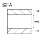
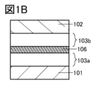
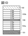
- 1A to 1E are diagrams illustrating the configuration of a light emitting device according to an embodiment.
- 2A to 2D are diagrams for explaining the light emitting device according to the embodiment.
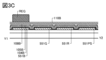
- 3A to 3C are diagrams for explaining the method for manufacturing the light emitting device according to the embodiment.
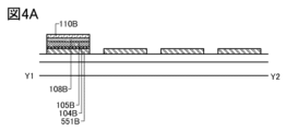
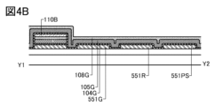
- 4A to 4C are diagrams for explaining the method for manufacturing the light emitting device according to the embodiment.
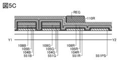
- 5A to 5C are diagrams for explaining the method for manufacturing the light emitting device according to the embodiment.
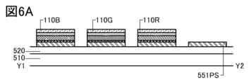
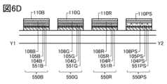
- 6A to 6D are diagrams for explaining the method for manufacturing the light emitting device according to the embodiment.
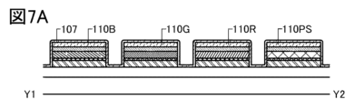
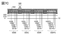
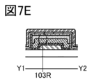
- 7A to 7E are diagrams illustrating the light emitting device according to the embodiment.
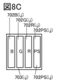
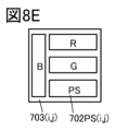
- 8A to 8F are diagrams for explaining the device and pixel arrangement according to the embodiment.
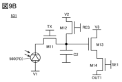
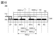
- FIGS. 9A to 9C are diagrams illustrating pixel circuits according to embodiments. 10A and 10B are diagrams for explaining a light emitting device according to an embodiment.
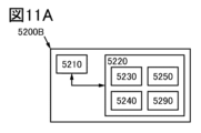
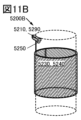
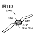
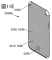
- FIG. 11A to 11E are diagrams for explaining the electronic device according to the embodiment.
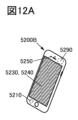
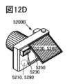
- 12A to 12E are diagrams illustrating electronic devices according to embodiments.
- 13A and 13B are diagrams for explaining the electronic device according to the embodiment.
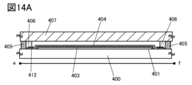
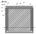
- 14A and 14B are diagrams illustrating the lighting device according to the embodiment.
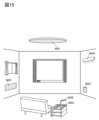
- FIG. 15 is a diagram illustrating a lighting device according to an embodiment; 16A to 16C are diagrams explaining a light emitting device and a light receiving device according to an embodiment.
- 17A and 17B are diagrams illustrating a light-emitting device and a light-receiving device according to an embodiment.
- FIGS 18A and 18B are 1 H-NMR spectra of Pn-mDBqPTzn.
- FIG. 19 shows absorption and emission spectra of Pn-mDBqPTzn in a dichloromethane solution.
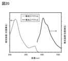
- FIG. 20 shows the absorption spectrum and emission spectrum of a thin film of Pn-mDBqPTzn.
- FIG. 21 shows emission spectra of light-emitting device 1 and light-emitting device 2.
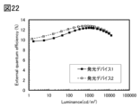
- FIG. FIG. 22 shows the external quantum efficiency-luminance characteristics of light-emitting device 1 and light-emitting device 2.
- FIG. FIG. 23 shows current-voltage characteristics of light-emitting device 1 and light-emitting device 2.
- FIG. FIG. FIG. 19 shows absorption and emission spectra of Pn-mDBqPTzn in a dichloromethane solution.
- FIG. 20 shows the absorption spectrum and emission spectrum of a thin film of Pn-mDBqPTzn.
- FIG. 21 shows emission spectra of light
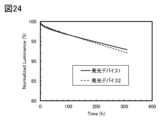
- FIG. 24 is a diagram showing changes in luminance with respect to driving time of light-emitting device 1 and light-emitting device 2 at room temperature.
- FIG. 25 is a diagram showing luminance changes with respect to driving time of light-emitting device 1 and light-emitting device 2 at 85°C.
- a compound of one embodiment of the present invention is an organic compound having an azine skeleton (also referred to as an azine compound).
- An azine skeleton refers to a skeleton in which one or more carbon atoms of a benzene ring are substituted with nitrogen, and examples thereof include a pyridine skeleton, a pyrazine skeleton, a pyrimidine skeleton, a pyridazine skeleton, and a triazine skeleton.
- a compound having an azine skeleton is, for example, an organic compound represented by general formula (G1) below.
- R 1 to R 7 each independently represent hydrogen (including deuterium), a substituted or unsubstituted alkyl group having 1 to 10 carbon atoms, a substituted or unsubstituted It preferably represents either an aryl group of 1 to 60 or a substituted or unsubstituted heteroaryl group of 1 to 60 carbon atoms.
- one of R 3 and R 4 preferably represents a condensed ring of 4 to 10 rings containing nitrogen as a ring-forming element.
- the other of R 3 and R 4 is either a substituted or unsubstituted condensed ring having 1 to 60 carbon atoms, a substituted or unsubstituted aryl group having a molecular weight of 78 or more, or a heteroaryl group having a molecular weight of 80 or more. It is preferable to express
- Having a condensed ring in R 3 or R 4 can improve carrier transport properties.
- the carrier transport property can be further improved.
- a condensed ring (curved condensed ring) having a helicene structure such as phenanthrene, triphenylene, or dibenzoquinoxaline
- the bandgap can be widened, and the T1 level and S1 level can be raised. can do.
- any one of A 1 to A 3 represents nitrogen, the others represent nitrogen or carbon, and in the case of carbon, each independently represents hydrogen (including deuterium), substituted or unsubstituted 1 to 10 carbon atoms is preferably bonded to any one of an alkyl group of , a substituted or unsubstituted aryl group having 1 to 60 carbon atoms, and a substituted or unsubstituted heteroaryl group having 1 to 60 carbon atoms.
- R 1 and R 2 each independently preferably include an aryl group with a molecular weight of 70 or more or a heteroaryl group with a molecular weight of 70 or more. It is also preferred that each of R 1 and R 2 independently includes an aryl group with a molecular weight of 150 or more or a heteroaryl group with a molecular weight of 150 or more.
- each of R 1 to R 4 preferably has a molecular weight of 70 or more and 1000 or less, more preferably 70 or more and 500 or less.
- R 3 or R 4 it is preferable to apply a condensed ring such as a naphthyl group rather than a phenyl group, and to use a substituent having a higher molecular weight than that of a phenyl group.
- molecular weights and atomic weights are expressed by rounding off to the first decimal place for the sake of simplicity.
- one of R 3 and R 4 represents general formula (G1-1), and the other of R 3 and R 4 represents general formula (G1-2) to general formula (G1- It is preferable to represent any one of 6).
- any one of A 11 to A 22 preferably represents nitrogen, the other one represents carbon, and the others each independently represent nitrogen or carbon.
- Any one of the carbon atoms of A 11 to A 22 is bonded to the general formula (G1), and the other is hydrogen (including deuterium), a substituted or unsubstituted alkyl group having 1 to 10 carbon atoms, a substituted or unsubstituted It is preferably bonded to either a substituted aryl group having 1 to 60 carbon atoms or a substituted or unsubstituted heteroaryl group having 1 to 60 carbon atoms.
- adjacent groups among the substituents bonded to A 11 to A 22 may be bonded to each other to form a ring.
- Forming a ring includes, for example, a structure in which one or more benzene rings containing A 12 and A 13 are added, in which case general formula (G1-1) includes five or more 6-membered rings It will be.
- general formula (G1-1) includes five or more 6-membered rings It will be.
- a substituted or unsubstituted vinyl group is included as a substituent bonded to A 11 to A 22 .
- general formulas (G1-2) to (G1-6) described later It should be noted that the ring-forming structure can also simply be said to be a structure further having a ring containing two of A 11 to A 22 .
- any one of A 41 to A 48 preferably represents carbon, and the others each independently represent nitrogen or carbon.
- any one of the carbon atoms of A 41 to A 48 is bonded to the general formula (G1), and the others are each independently hydrogen (including deuterium) or a substituted or unsubstituted alkyl group having 1 to 10 carbon atoms , a substituted or unsubstituted aryl group having 1 to 60 carbon atoms, or a substituted or unsubstituted heteroaryl group having 1 to 60 carbon atoms.
- adjacent groups among the substituents bonded to A 41 to A 48 may be bonded to each other to form a ring.
- any one of A 51 to A 60 preferably represents carbon, and the others each independently represent nitrogen or carbon.
- any one of the carbon atoms of A 51 to A 60 is bonded to the general formula (G1), and the others are each independently hydrogen (including deuterium) or a substituted or unsubstituted alkyl group having 1 to 10 carbon atoms , a substituted or unsubstituted aryl group having 1 to 60 carbon atoms, or a substituted or unsubstituted heteroaryl group having 1 to 60 carbon atoms.
- adjacent groups may be bonded to each other to form a ring.
- any one of A 61 to A 68 preferably represents carbon, and the others each independently represent nitrogen or carbon.
- a 69 preferably represents nitrogen, carbon, sulfur or oxygen.
- any one of the carbons of A 61 to A 68 or the nitrogen of A 69 is bonded to the general formula (G1), and the others are each independently hydrogen (including deuterium), substituted or unsubstituted carbon number 1 It preferably represents any one of an alkyl group having 1 to 10 carbon atoms, a substituted or unsubstituted aryl group having 1 to 60 carbon atoms, and a substituted or unsubstituted heteroaryl group having 1 to 60 carbon atoms.
- adjacent groups may be bonded to each other to form a ring.
- any one of A 71 to A 80 preferably represents carbon, and the others each independently represent nitrogen or carbon.
- any one of the carbon atoms of A 71 to A 80 is bonded to the general formula (G1), and the others are each independently hydrogen (including deuterium) or a substituted or unsubstituted alkyl group having 1 to 10 carbon atoms , a substituted or unsubstituted aryl group having 1 to 60 carbon atoms, and a substituted or unsubstituted heteroaryl group having 1 to 60 carbon atoms.
- adjacent groups may be bonded to each other to form a ring.
- any one of A 81 to A 92 preferably represents carbon, and the others each independently represent nitrogen or carbon.
- any one of the carbon atoms of A 81 to A 92 is bonded to the general formula (G1), and the others are each independently hydrogen (including deuterium) or a substituted or unsubstituted alkyl group having 1 to 10 carbon atoms , a substituted or unsubstituted aryl group having 1 to 60 carbon atoms, and a substituted or unsubstituted heteroaryl group having 1 to 60 carbon atoms.
- adjacent groups among the substituents bonded to A 81 to A 92 may be bonded to each other to form a ring.
- An organic compound of one embodiment of the present invention is an organic compound represented by General Formula (G2) below.
- R 8 to R 17 each independently represent hydrogen (including deuterium), a substituted or unsubstituted alkyl group having 1 to 10 carbon atoms, a substituted or unsubstituted aryl group having 1 to 60 carbon atoms, and It preferably represents either a substituted or unsubstituted heteroaryl group having 1 to 60 carbon atoms. Adjacent groups among R 8 to R 17 may combine with each other to form a ring.
- An organic compound of one embodiment of the present invention is an organic compound represented by General Formula (G3) below.
- R 18 to R 21 each independently represent hydrogen (including deuterium), a substituted or unsubstituted alkyl group having 1 to 10 carbon atoms, a substituted or unsubstituted aryl group having 1 to 60 carbon atoms, and It preferably represents either a substituted or unsubstituted heteroaryl group having 1 to 60 carbon atoms. Adjacent groups among R 18 to R 21 may be bonded to each other to form a ring. Moreover, m represents 1 or 2. In addition, the binding position of R 4 may be any of the meta, para, and ortho positions, but the meta position can lower the sublimation temperature, and the para position can increase the Tg. .
- An organic compound of one embodiment of the present invention is an organic compound represented by General Formula (G4) below.
- R 18 to R 25 each independently represent hydrogen (including deuterium), a substituted or unsubstituted alkyl group having 1 to 10 carbon atoms, a substituted or unsubstituted aryl group having 1 to 60 carbon atoms, and It preferably represents either a substituted or unsubstituted heteroaryl group having 1 to 60 carbon atoms. Adjacent groups among R 18 to R 25 may combine with each other to form a ring. Moreover, m represents 1 or 2. Moreover, n represents 1 or 2. In addition, the bonding position of R 3 and R 4 may be any of the meta, para, and ortho positions, but the meta position can lower the sublimation temperature, and the para position increases Tg. be able to.
- the glass transition temperature Tg of the compound of one embodiment of the present invention is preferably 100° C. or higher. Further, the glass transition temperature Tg of the compound of one embodiment of the present invention is preferably 120° C. or higher, preferably 130° C. or higher, more preferably 140° C. or higher, still more preferably 150° C. or higher, particularly 160° C. or higher.
- the compound of one embodiment of the present invention preferably has a solubility of 0% or more and less than 5%.
- solubility % by weight is evaluated as follows. Solute A (g) and solvent B (g) are put into a glass container, and if no precipitate is visually observed, the solubility is (A / (A + B) ⁇ 100)% or more, and the precipitate is confirmed. If so, the solubility is determined to be less than (A/(A+B) x 100)%.
- a 1 to A 92 or R 1 to R 25 in the general formulas (G1) to (G4) may be applied in combination.
- a structure in which "R 3 and R 4 both have three or more condensed rings, and R 4 contains nitrogen” may be combined with the constitution that the molecular weight of R 2 is 70 or more.
- synergistic effects such as improvement in glass transition temperature Tg, improvement in stability, and improvement in stability of film quality in a thin film state can be obtained.
- alkyl group having 1 to 10 carbon atoms include methyl group, ethyl group, propyl group, isopropyl group, butyl group, sec-butyl group, isobutyl group, tert -butyl group, pentyl group, isopentyl group, sec-pentyl group, tert-pentyl group, neopentyl group, hexyl group, isohexyl group, sec-hexyl group, tert-hexyl group, neohexyl group, 3-methylpentyl group, 2- methylpentyl group, 2-ethylbutyl group, 1,2-dimethylbutyl group, 2,3-dimethylbutyl group and the like.
- substituted or unsubstituted aryl group having 6 to 60 carbon atoms and the substituted or unsubstituted heteroaryl group having 2 to 50 carbon atoms include substituted or unsubstituted phenyl group, biphenyl group, terphenyl group, fluorenyl group, spirobifluorenyl group, naphthyl group, anthracenyl group, phenanthryl group, fluoranthenyl group, pyrenyl group, chrysenyl group, triphenylenyl group, perylenyl group, indenyl group, benzoindenyl group, pyrrolyl group, indolyl group, carbazolyl group, furanyl group, benzofuranyl group, dibenzofuranyl group, thiophenyl group, benzothiophenyl group, dibenzothiophenyl group, imidazoly
- the compound of one embodiment of the present invention is used for a light-emitting device, it is preferably a thin film (also referred to as an organic compound layer).
- a thin film containing an organic compound which is one embodiment of the present invention, can be used as a charge adjustment layer, a charge generation layer, a light-emitting layer, a hole injection layer, a hole transport layer, an electron transport layer, an electron injection layer, or a cap layer in a light-emitting device. It can be used preferably.
- the organic compound according to one embodiment of the present invention can also be used for non-light-emitting devices. Examples of non-light-emitting devices include devices such as light-receiving devices.
- the organic compound represented by general formula (G1) can be synthesized according to the following synthesis schemes (a-1) to (a-5).
- compound 3 can be obtained by coupling compound 1 having an azine skeleton and compound 2 having R 1 .
- compound 5 can be obtained by coupling compound 3 with compound 4 having R 2 according to reaction formula (a-2).
- compound 7 can be obtained by coupling compound 5 and compound 6 according to reaction formula (a-3).
- compound 9 can be obtained by coupling compound 7 with compound 8 having R 3 according to reaction scheme (a-4).
- the compound represented by general formula (G1) can be obtained by coupling compound 9 with compound 10 having R 4 according to reaction scheme (a-5).
- X1 to X5 each represent a halogen group (eg, containing chlorine).
- B1 to B5 each represent a boronic acid.
- X 1 to X 5 and B 1 to B 5 are each independently chlorine, bromine, iodine, triflate group, organic boron group, boronic acid, organic aluminum, organic zirconium, organic zinc, organic A tin base or the like may also be used.
- R 3 and R 4 have different substituent structures, it is preferable that one of X 4 and X 5 is chlorine and the other is bromine or iodine.
- Synthesis schemes (a-1) to (a-5) can be performed, for example, by Suzuki-Miyaura coupling reaction.
- the palladium catalyst includes palladium(II) acetate, tetrakis(triphenylphosphine)palladium(0), bis(triphenylphosphine)palladium(II) dichloride, and the like.
- tri(ortho-tolyl)phosphine, triphenylphosphine, tricyclohexylphosphine and the like can be mentioned as ligands for palladium catalysts.
- Examples of the base that can be used in the reactions of the synthesis schemes (a-1) to (a-5) include organic bases such as sodium-tert-butoxide, potassium carbonate, sodium carbonate, potassium phosphate, potassium acetate and the like. Inorganic bases and the like are included.
- Solvents that can be used in the reactions of the synthesis schemes (a-1) to (a-5) include a mixed solvent of toluene and water, a mixed solvent of alcohol such as toluene and ethanol and water, and a mixture of xylene and water.
- Solvents include a mixed solvent of alcohol and water such as xylene and ethanol, a mixed solvent of benzene and water, a mixed solvent of alcohol and water such as benzene and ethanol, and a mixed solvent of ether and water such as diethylene glycol dimethyl ether.
- a mixed solvent of toluene and water, a mixed solvent of toluene, ethanol and water, and a mixed solvent of water and an ether such as diethylene glycol dimethyl ether are more preferable.
- R 1 to R 7 may be deuterium. Further, the substituents of A 1 to A 3 or the substituents of R 1 to R 7 may be deuterium. In that case, a compound obtained by deuterating compound 1, compound 2, compound 4, compound 6, compound 8, or compound 10 may be used for the coupling reaction. Solvents that can be used in the deuteration reaction include benzene-d6, toluene-d8, xylene-d10, heavy water, and the like.
- Catalysts that can be used include molybdenum (V) chloride, tungsten (VI) chloride, niobium (V) chloride, tantalum (V) chloride, aluminum (III) chloride, titanium (IV) chloride, and tin (IV) chloride. etc.
- the solvent and catalyst are not limited to these.
- X 6 to X 10 and B 6 to B 10 each independently represent hydrogen, chlorine, bromine, iodine, triflate group, organic boron group, boronic acid, organic aluminum, organic zirconium, organic zinc, organic tin group, or the like. Point.
- the conditions (palladium catalyst, solvent, etc.) used for the coupling reaction can be the methods shown in Reaction Formulas (a-1) to (a-5).
- a compound represented by general formula (G2) or general formula (G3) can also be synthesized by a similar synthesis method.
- the above synthetic method is an example, and it is possible to produce the compound of the present application using other synthetic methods.
- Embodiment 2 In this embodiment mode, a structure of a light-emitting device using the organic compound described in Embodiment Mode 1 will be described with reference to FIGS. 1A to 1E.
- FIG. 1A shows a light-emitting device having an EL layer that includes a light-emitting layer between a pair of electrodes. Specifically, it has a structure in which an EL layer 103 is sandwiched between a first electrode 101 and a second electrode 102 .
- FIG. 1B shows a laminated structure (tandem structure) having a plurality of (two layers in FIG. 1B) EL layers (103a and 103b) between a pair of electrodes and a charge generation layer 106 between the EL layers. of the light emitting device.
- a light-emitting device with a tandem structure can realize a highly efficient light-emitting device without changing the amount of current.
- the charge generation layer 106 injects electrons into one EL layer (103a or 103b) and injects electrons into the other EL layer (103b or 103a) has a function of injecting holes. Therefore, in FIG. 1B, when a voltage is applied to the first electrode 101 so that the potential is higher than that of the second electrode 102, electrons are injected from the charge generation layer 106 into the EL layer 103a, and the EL layer 103b is positively charged. A hole is to be injected.
- the charge generation layer 106 may have a property of transmitting visible light (specifically, the visible light transmittance of the charge generation layer 106 is 40% or more). preferable. Also, the charge generation layer 106 functions even with a lower conductivity than the first electrode 101 and the second electrode 102 .
- the compound of the present application can also be used in the layer into which electrons are injected in the charge generation layer. In that case, it is preferable to use a mixed layer or laminated structure of a Li compound such as Li metal or lithium oxide and the compound of the present application.
- FIG. 1C shows a stacked structure of the EL layer 103 of the light-emitting device which is one embodiment of the present invention.
- the first electrode 101 functions as an anode and the second electrode 102 functions as a cathode.
- the EL layer 103 has a structure in which a hole-injection layer 111, a hole-transport layer 112, a light-emitting layer 113, an electron-transport layer 114, and an electron-injection layer 115 are sequentially stacked over the first electrode 101.
- the light-emitting layer 113 may have a structure in which a plurality of light-emitting layers emitting light of different colors are stacked.
- a light-emitting layer containing a light-emitting substance that emits red light, a light-emitting layer that contains a light-emitting substance that emits green light, and a light-emitting layer that contains a light-emitting substance that emits blue light are stacked, or a layer containing a carrier-transporting material is interposed therebetween. It may be a laminated structure. Alternatively, a light-emitting layer containing a light-emitting substance that emits yellow light and a light-emitting layer containing a light-emitting substance that emits blue light may be combined. However, the laminated structure of the light-emitting layer 113 is not limited to the above.
- the light-emitting layer 113 may have a structure in which a plurality of light-emitting layers emitting light of the same color are stacked.
- a structure in which a first light-emitting layer containing a light-emitting substance that emits blue light and a second light-emitting layer containing a light-emitting substance that emits blue light are stacked or stacked with a layer containing a carrier-transporting material interposed therebetween. It can be.
- reliability may be improved as compared with a single-layer structure.
- each EL layer is stacked sequentially from the anode side as described above.
- the stacking order of the EL layers 103 is reversed.
- 111 on the first electrode 101 which is a cathode is an electron injection layer
- 112 is an electron transport layer
- 113 is a light emitting layer
- 114 is a hole transport layer
- 115 is a hole. It has a structure called an injection layer.
- the light-emitting layer 113 included in the EL layers (103, 103a, and 103b) includes a light-emitting substance and an appropriate combination of a plurality of substances, and has a structure in which fluorescence or phosphorescence with a desired emission color can be obtained.
- the light-emitting layer 113 may have a laminated structure with different emission colors. Note that in this case, different materials may be used for the light-emitting substance and other substances used in the stacked light-emitting layers. Alternatively, a structure in which different emission colors are obtained from the plurality of EL layers (103a and 103b) shown in FIG. 1B may be employed. In this case also, different materials may be used for the light-emitting substance and other substances used in each light-emitting layer.
- the light-emitting device which is one embodiment of the present invention, for example, the first electrode 101 shown in FIG. ) structure
- light emitted from the light-emitting layer 113 included in the EL layer 103 can be resonated between the two electrodes, and light emitted from the second electrode 102 can be enhanced.
- the film of the transparent conductive film Optical tuning can be achieved by controlling the thickness. Specifically, the optical distance between the first electrode 101 and the second electrode 102 (the product of the film thickness and the refractive index) is m ⁇ / It is preferable to adjust to 2 (where m is an integer equal to or greater than 1) or its vicinity.
- the optical distance from the first electrode 101 to the region (light-emitting region) of the light-emitting layer 113 from which desired light is obtained is (2m′+1) ⁇ /4 (where m′ is an integer equal to or greater than 1) or the vicinity thereof. It is preferable to adjust so that Note that the light-emitting region here means a recombination region of holes and electrons in the light-emitting layer 113 .
- the optical distance between the first electrode 101 and the second electrode 102 is the total thickness from the reflection area of the first electrode 101 to the reflection area of the second electrode 102. can.
- the optical distance between the first electrode 101 and the light-emitting layer from which desired light is obtained is the optical distance between the reflection region in the first electrode 101 and the light-emitting region in the light-emitting layer from which desired light is obtained. It can be said that it is the distance.
- an arbitrary position of the first electrode 101 can be used as the reflective region and the desired light.
- an arbitrary position of the light-emitting layer from which light is obtained is the light-emitting region, the above effects can be sufficiently obtained.
- the light-emitting device shown in FIG. 1D is a light-emitting device having a tandem structure and has a microcavity structure, so that light of different wavelengths (monochromatic light) can be extracted from each EL layer (103a, 103b). Therefore, separate coloring (for example, RGB) for obtaining different emission colors is unnecessary. Therefore, it is easy to achieve high definition. A combination with a colored layer (color filter) is also possible. Furthermore, since it is possible to increase the emission intensity of the specific wavelength in the front direction, it is possible to reduce power consumption.
- the light-emitting device shown in FIG. 1E is an example of the tandem structure light-emitting device shown in FIG. It has a structure in which it is sandwiched and laminated.
- the three EL layers (103a, 103b, 103c) each have a light-emitting layer (113a, 113b, 113c), and the emission colors of the respective light-emitting layers can be freely combined.
- light-emitting layer 113a can be blue
- light-emitting layer 113b can be either red, green, or yellow
- light-emitting layer 113c can be blue
- light-emitting layer 113a can be red and light-emitting layer 113b can be blue, green, or yellow.
- the light-emitting layer 113c may be red.
- the light-emitting layer 113a, the light-emitting layer 113b, and the light-emitting layer 113c may be fluorescent light-emitting layers or phosphorescent light-emitting layers.
- each of the light-emitting layer 113a, the light-emitting layer 113b, and the light-emitting layer 113c may be an independent light-emitting layer, or may be a laminated light-emitting layer of two or more layers.
- the light-emitting layer 113a, the light-emitting layer 113b, and the light-emitting layer 113c are stacked light-emitting layers of two or more layers
- the light-emitting layer 113a is blue
- the light-emitting layer 113b is a three-layer stack of red, yellow, and green
- the light-emitting layer 113c is It may be blue.
- the light-emitting layer 113a, the light-emitting layer 113b, and the light-emitting layer 113c are laminated light-emitting layers of two or more layers
- the light-emitting layer 113a is blue
- the light-emitting layers 113b are red and yellow
- the light-emitting layer 113c is blue.
- the light-emitting layer 113a, the light-emitting layer 113b, and the light-emitting layer 113c are laminated light-emitting layers of two or more layers
- the light-emitting layer 113a is blue
- the light-emitting layer 113b is red, yellow, yellow, and green.
- 113c may be blue.
- the first electrode 101 and the second electrode 102 is a light-transmitting electrode (a transparent electrode, a semi-transmissive/semi-reflective electrode, or the like). do.
- the visible light transmittance of the transparent electrode is set to 40% or more.
- the visible light reflectance of the semi-transmissive/semi-reflective electrode should be 20% or more and 80% or less, preferably 40% or more and 70% or less.
- these electrodes preferably have a resistivity of 1 ⁇ 10 ⁇ 2 ⁇ cm or less.
- the reflective electrode when one of the first electrode 101 and the second electrode 102 is a reflective electrode (reflective electrode), the reflective electrode The light reflectance is 40% or more and 100% or less, preferably 70% or more and 100% or less. Moreover, the electrode preferably has a resistivity of 1 ⁇ 10 ⁇ 2 ⁇ cm or less.
- FIGS. 1A and 1B the compound of one embodiment of the present application can be used for a single-color tandem light-emitting device in which separate colors are not used, or a light-emitting device with a separate color structure.
- a monochromatic tandem light-emitting device can also be used for a full-color display by combining it with a color filter or color conversion layer.
- FIG. 1D having a tandem structure.
- the structure of the EL layer is the same for the single-structure light-emitting device shown in FIGS. 1A and 1C.
- the first electrode 101 is formed as a reflective electrode
- the second electrode 102 is formed as a semi-transmissive/semi-reflective electrode. Therefore, a desired electrode material can be used singly or plurally to form a single layer or lamination.
- the second electrode 102 is formed by selecting an appropriate material after the EL layer 103b is formed.
- First electrode and second electrode> As materials for forming the first electrode 101 and the second electrode 102, the following materials can be used in appropriate combination as long as the above-described functions of both electrodes can be satisfied. For example, metals, alloys, electrically conductive compounds, mixtures thereof, and the like can be used as appropriate. Specifically, In--Sn oxide (also referred to as ITO), In--Si--Sn oxide (also referred to as ITSO), In--Zn oxide, and In--W--Zn oxide are given.
- ITO In--Sn oxide
- ITSO In--Si--Sn oxide
- ITSO In--Zn oxide
- In--W--Zn oxide In--W--Zn oxide
- elements belonging to Group 1 or Group 2 of the periodic table of elements not exemplified above e.g., lithium (Li), cesium (Cs), calcium (Ca), strontium (Sr)), europium (Eu), ytterbium Rare earth metals such as (Yb), alloys containing an appropriate combination thereof, graphene, and the like can be used.
- a hole-injection layer 111a and a hole-transport layer 112a of the EL layer 103a are sequentially stacked on the first electrode 101 by vacuum deposition. be.
- hole injection layer 111b and hole transport layer 112b of EL layer 103b are sequentially laminated on charge generation layer 106 in the same manner.
- the hole injection layers (111, 111a, 111b) inject holes from the first electrode 101, which is an anode, and the charge generation layers (106, 106a, 106b) into the EL layers (103, 103a, 103b). It is a layer containing an organic acceptor material and a material with a high hole injection property.
- organic acceptor material causes a charge separation between its LUMO level (lowest unoccupied molecular orbital) and another organic compound having a similar HOMO level value, so that holes ( It is a material that can generate holes. Therefore, compounds having electron-withdrawing groups (halogen groups or cyano groups) such as quinodimethane derivatives, chloranil derivatives, and hexaazatriphenylene derivatives can be used as organic acceptor materials.
- a compound in which an electron-withdrawing group is bound to a condensed aromatic ring having a plurality of heteroatoms such as HAT-CN, is suitable because it has a high acceptor property and stable film quality against heat.
- [3] radialene derivatives having an electron-withdrawing group are preferred because of their extremely high electron-accepting properties, specifically ⁇ , ⁇ ', ⁇ '.
- Materials with high hole injection properties include oxides of metals belonging to groups 4 to 8 in the periodic table (molybdenum oxide, vanadium oxide, ruthenium oxide, tungsten oxide, manganese oxide, etc.). transition metal oxides, etc.) can be used. Specific examples include molybdenum oxide, vanadium oxide, niobium oxide, tantalum oxide, chromium oxide, tungsten oxide, manganese oxide, and rhenium oxide. Among the above, molybdenum oxide is preferred because it is stable in the atmosphere, has low hygroscopicity, and is easy to handle. In addition, a phthalocyanine-based compound such as phthalocyanine (abbreviation: H 2 Pc) or copper phthalocyanine (abbreviation: CuPc) can be used.
- H 2 Pc phthalocyanine
- CuPc copper phthalocyanine
- low-molecular-weight compounds such as 4,4′,4′′-tris(N,N-diphenylamino)triphenylamine (abbreviation: TDATA) and 4,4′,4′′-tris [N-(3-methylphenyl)-N-phenylamino]triphenylamine (abbreviation: MTDATA), 4,4′-bis[N-(4-diphenylaminophenyl)-N-phenylamino]biphenyl (abbreviation: DPAB), N,N'-bis ⁇ 4-[bis(3-methylphenyl)amino]phenyl ⁇ -N,N'-diphenylbiphenyl-4,4'-diamine (abbreviation: DNTPD), 1,3,5 -tris[N-(4-diphenylaminophenyl)-N-phenylamino]benzene (abbreviation: DPA3B), 3-[N-(9-
- poly(N-vinylcarbazole) (abbreviation: PVK)
- poly(4-vinyltriphenylamine) (abbreviation: PVTPA)
- PVTPA poly(4-vinyltriphenylamine)
- PTPDMA poly[N-(4 - ⁇ N'-[4-(4-diphenylamino)phenyl]phenyl-N'-phenylamino ⁇ phenyl)methacrylamide]
- PTPDMA poly[N,N'-bis(4-butylphenyl)- N,N'-bis(phenyl)benzidine]
- Poly-TPD poly(N-vinylcarbazole) or the like
- PEDOT/PSS poly(3,4-ethylenedioxythiophene)/polystyrene sulfonic acid
- PAni/PSS polyaniline/polystyrene sulfonic acid
- other acid-added polymer compounds etc.
- a mixed material containing a hole transporting material and the above-described organic acceptor material can also be used.
- electrons are extracted from the hole-transporting material by the organic acceptor material, holes are generated in the hole-injection layer 111 , and holes are injected into the light-emitting layer 113 via the hole-transporting layer 112 .
- the hole injection layer 111 may be formed of a single layer made of a mixed material containing a hole-transporting material and an organic acceptor material (electron-accepting material). (electron-accepting material) may be laminated in separate layers.
- the hole-transporting material a substance having a hole mobility of 1 ⁇ 10 ⁇ 6 cm 2 /Vs or more at a square root of an electric field strength [V/cm] of 600 is preferable. Note that any substance other than these can be used as long as it has a higher hole-transport property than electron-transport property.
- hole-transporting materials include compounds having a ⁇ -electron-rich heteroaromatic ring (e.g., carbazole derivatives, furan derivatives, or thiophene derivatives), and positive compounds such as aromatic amines (organic compounds having an aromatic amine skeleton). Materials with high pore transport properties are preferred. Since the compound of Embodiment 1 has a hole-transport property, it can also be used as a hole-transport material.
- carbazole derivatives organic compounds having a carbazole ring
- examples of the carbazole derivatives include bicarbazole derivatives (eg, 3,3'-bicarbazole derivatives) and aromatic amines having a carbazolyl group.
- bicarbazole derivative for example, 3,3′-bicarbazole derivative
- PCCP 3,3′-bis(9-phenyl-9H-carbazole)
- BisBPCz 9,9 '-Bis(biphenyl-4-yl)-3,3'-bi-9H-carbazole
- BismBPCz 9,9'-bis(biphenyl-3-yl)-3,3'-bi-9H- Carbazole
- BismBPCz 9-(biphenyl-3-yl)-9′-(biphenyl-4-yl)-9H,9′H-3,3′-bicarbazole
- mBPCCBP 9-( 2-naphthyl)-9′-phenyl-9H,9′H-3,3′-bicarbazole
- ⁇ NCCP 9-( 2-naphthyl)-9′-phenyl-9H,9′H-3,3′-bicarbazole
- aromatic amine having a carbazolyl group examples include 4-phenyl-4′-(9-phenyl-9H-carbazol-3-yl)triphenylamine (abbreviation: PCBA1BP), N-( 4-biphenyl)-N-(9,9-dimethyl-9H-fluoren-2-yl)-9-phenyl-9H-carbazol-3-amine (abbreviation: PCBiF), N-(biphenyl-4-yl)- N-[4-(9-phenyl-9H-carbazol-3-yl)phenyl]-9,9-dimethyl-9H-fluoren-2-amine (abbreviation: PCBBiF), N-[4-(9-phenyl- 9H-carbazol-3-yl)phenyl]-bis(9,9-dimethyl-9H-fluoren-2-yl)amine (abbreviation: PCBFF), N-(biphenyl-4-yl)-N-(b
- PCPPn 3-[4-(9-phenanthryl)-phenyl]-9-phenyl-9H-carbazole
- PCPN 3-[4-(1-naphthyl)- Phenyl]-9-phenyl-9H-carbazole
- mCP 1,3-bis(N-carbazolyl)benzene
- CBP 4,4′-di(N-carbazolyl)biphenyl
- CzTP 3,6-bis(3,5-diphenylphenyl)-9-phenylcarbazole
- TCPB 1,3,5-tris[4-(N-carbazolyl)phenyl]benzene
- TCPB 9 -[4-(10-phenyl-9-anthracenyl)phenyl]-9H-carbazole
- furan derivative an organic compound having a furan ring
- DBF3P- II 4,4′,4′′-(benzene-1,3,5-triyl)tri(dibenzofuran)
- mmDBFFLBi-II 4- ⁇ 3-[3-(9-phenyl-9H-fluoren-9-yl)phenyl]phenyl ⁇ dibenzofuran
- thiophene derivative an organic compound having a thiophene ring
- DBT3P 4,4′,4′′-(benzene-1,3,5-triyl)tri(dibenzothiophene)
- DBT3P 4,4′,4′′-(benzene-1,3,5-triyl)tri(dibenzothiophene)
- DBTFLP-III 2,8-diphenyl-4-[4-(9-phenyl-9H-fluoren-9-yl)phenyl]dibenzothiophene
- DBTFLP-III 4-[4-(9-phenyl- 9H-fluoren-9-yl)phenyl]-6-phenyldibenzothiophene
- DBTFLP-IV 4-[4-(9-phenyl- 9H-fluoren-9-yl)phenyl]-6-phenyldibenzothiophene
- aromatic amine examples include 4,4′-bis[N-(1-naphthyl)-N-phenylamino]biphenyl (abbreviation: NPB or ⁇ -NPD), N,N′- Bis(3-methylphenyl)-N,N'-diphenyl-biphenyl-4,4'-diamine (abbreviation: TPD), 4,4'-bis[N-(spiro-9,9'-bifluorene-2- yl)-N-phenylamino]biphenyl (abbreviation: BSPB), 4-phenyl-4′-(9-phenylfluoren-9-yl)triphenylamine (abbreviation: BPAFLP), 4-phenyl-3′-(9 -phenylfluoren-9-yl)triphenylamine (abbreviation: mBPAFLP), N-(9,9-dimethyl-9H-fluoren-2-yl)
- poly(N-vinylcarbazole) (abbreviation: PVK) and poly(4-vinyltriphenylamine) (abbreviation: PVK), which are high molecular compounds (oligomers, dendrimers, polymers, etc.) PVTPA), poly[N-(4- ⁇ N'-[4-(4-diphenylamino)phenyl]phenyl-N'-phenylamino ⁇ phenyl)methacrylamide] (abbreviation: PTPDMA), poly[N,N' -Bis(4-butylphenyl)-N,N'-bis(phenyl)benzidine] (abbreviation: Poly-TPD) and the like can be used.
- PVK poly(N-vinylcarbazole)
- PVK poly(4-vinyltriphenylamine)
- PVTPA high molecular compounds (oligomers, dendrimers, polymers, etc.) PVTPA)
- PTPDMA
- PEDOT/PSS poly(3,4-ethylenedioxythiophene)/polystyrene sulfonic acid
- PAni/PSS polyaniline/polystyrene sulfonic acid
- other acid-added polymer compounds etc.
- the hole-transporting material is not limited to the above, and one or a combination of various known materials may be used as the hole-transporting material.
- the hole injection layers (111, 111a, 111b) can be formed using various known film forming methods, and can be formed using, for example, a vacuum deposition method.
- the hole transport layers (112, 112a, 112b) transport holes injected from the first electrode 101 by the hole injection layers (111, 111a, 111b) to the light emitting layers (113, 113a, 113b). layer.
- the hole-transporting layers (112, 112a, 112b) are layers containing a hole-transporting material. Therefore, for the hole transport layers (112, 112a, 112b), a hole transport material that can be used for the hole injection layers (111, 111a, 111b) can be used.
- the same organic compound as that for the hole-transport layers (112, 112a, and 112b) can be used for the light-emitting layers (113, 113a, 113b, and 113c).
- the hole transport layers (112, 112a, 112b) and the light emitting layers (113, 113a, 113b, 113c) can be efficiently transported, which is more preferable.
- the light-emitting layers (113, 113a, 113b, 113c) are layers containing light-emitting substances.
- a light-emitting substance that can be used for the light-emitting layers (113, 113a, 113b, and 113c) a substance that emits light such as blue, purple, blue-violet, green, yellow-green, yellow, orange, or red is used as appropriate. be able to.
- a structure in which different light-emitting substances are used for each light-emitting layer to exhibit different emission colors for example, white light emission obtained by combining complementary emission colors
- a laminated structure in which one light-emitting layer contains different light-emitting substances may be employed.
- the light-emitting layers may contain one or more organic compounds (host material, etc.) in addition to the light-emitting substance (guest material).
- the newly added second host material has an energy gap larger than that of the existing guest materials and the first host material. It is preferred to use a substance having The lowest singlet excitation energy level (S1 level) of the second host material is higher than the S1 level of the first host material, and the lowest triplet excitation energy level (T1 level) of the second host material is higher than the S1 level of the first host material. level) is preferably higher than the T1 level of the guest material. Also, the lowest triplet excitation energy level (T1 level) of the second host material is preferably higher than the T1 level of the first host material.
- an exciplex can be formed from two kinds of host materials. Note that in order to efficiently form an exciplex, it is particularly preferable to combine a compound that easily accepts holes (a hole-transporting material) and a compound that easily accepts electrons (an electron-transporting material). Also, with this configuration, high efficiency, low voltage, and long life can be achieved at the same time.
- the organic compound used as the above host material may be the hole transport layer (112, 112a, 112b), or an electron-transporting material that can be used in the later-described electron-transporting layers (114, 114a, 114b).
- An exciplex composed of compounds (the first host material and the second host material described above) may be used. Note that an exciplex (also referred to as an exciplex, or an exciplex) in which multiple kinds of organic compounds form an excited state has an extremely small difference between the S1 level and the T1 level, and triplet excitation energy is reduced to singlet excitation. It has a function as a TADF material that can be converted into energy.
- an exciplex As a combination of a plurality of types of organic compounds that form an exciplex, for example, it is preferable that one has a ⁇ -electron-deficient heteroaromatic ring and the other has a ⁇ -electron-rich heteroaromatic ring.
- an organometallic complex based on iridium, rhodium, or platinum, or a phosphorescent substance such as a metal complex may be used. Since the organic compound described in Embodiment 1 has an electron-transport property, it can be effectively used as the first host material. Moreover, since it has a hole-transport property, it can be used as a second host material.
- the light-emitting substance that can be used in the light-emitting layers (113, 113a, 113b, 113c) is not particularly limited, and a light-emitting substance that converts singlet excitation energy into light emission in the visible light region, or a light-emitting substance that converts triplet excitation energy into light in the visible light region.
- Luminescent substances that convert to luminescence can be used.
- ⁇ Luminescent substances that convert singlet excitation energy into luminescence As a light-emitting substance that converts singlet excitation energy into light emission and that can be used for the light-emitting layers (113, 113a, 113b, and 113c), the following substances that emit fluorescence (fluorescent light-emitting substances) are listed.
- Examples thereof include pyrene derivatives, anthracene derivatives, triphenylene derivatives, fluorene derivatives, carbazole derivatives, dibenzothiophene derivatives, dibenzofuran derivatives, dibenzoquinoxaline derivatives, quinoxaline derivatives, pyridine derivatives, pyrimidine derivatives, phenanthrene derivatives, naphthalene derivatives and the like. Pyrene derivatives are particularly preferred because they have a high emission quantum yield.
- pyrene derivatives include N,N'-bis(3-methylphenyl)-N,N'-bis[3-(9-phenyl-9H-fluoren-9-yl)phenyl]pyrene-1,6 - diamine (abbreviation: 1,6mMemFLPAPrn), N,N'-diphenyl-N,N'-bis[4-(9-phenyl-9H-fluoren-9-yl)phenyl]pyrene-1,6-diamine (abbreviation: : 1,6FLPAPrn), N,N'-bis(dibenzofuran-2-yl)-N,N'-diphenylpyrene-1,6-diamine (abbreviation: 1,6FrAPrn), N,N'-bis(dibenzothiophene -2-yl)-N,N'-diphenylpyrene-1,6-diamine (abbreviation: 1,6ThAPrn),
- N-[9,10-bis(biphenyl-2-yl)-2-anthryl]-N,9-diphenyl-9H-carbazol-3-amine abbreviation: 2PCABPhA
- N-(9,10-diphenyl -2-anthryl)-N,N',N'-triphenyl-1,4-phenylenediamine abbreviation: 2DPAPA
- N-[9,10-bis(biphenyl-2-yl)-2-anthryl]- N,N',N'-triphenyl-1,4-phenylenediamine abbreviation: 2DPABPhA
- 9,10-bis(biphenyl-2-yl)-N-[4-(9H-carbazol-9-yl) Phenyl]-N-phenylanthracen-2-amine abbreviation: 2YGABPhA
- N,N,9-triphenylanthracen-9-amine abbreviation: 2Y
- the light-emitting substance that converts triplet excitation energy into light emission includes, for example, a substance that emits phosphorescence (phosphorescent light-emitting substance), or a thermally activated delayed fluorescence that exhibits thermally activated delayed fluorescence. (Thermally activated delayed fluorescence: TADF) materials.
- a phosphorescent substance is a compound that exhibits phosphorescence and does not exhibit fluorescence in any of the temperature range from low temperature (for example, 77K) to room temperature (that is, from 77K to 313K).
- the phosphorescent substance preferably contains a metal element having a large spin-orbit interaction, and examples thereof include organometallic complexes, metal complexes (platinum complexes), rare earth metal complexes, and the like.
- a transition metal element is preferred, and in particular a platinum group element (ruthenium (Ru), rhodium (Rh), palladium (Pd), osmium (Os), iridium (Ir), or platinum (Pt)) may be included.
- iridium is preferable because the transition probability associated with the direct transition between the singlet ground state and the triplet excited state can be increased.
- phosphorescent substance (450 nm or more and 570 nm or less: blue or green)>>>>>> Examples of phosphorescent substances that exhibit blue or green color and have an emission spectrum with a peak wavelength of 450 nm or more and 570 nm or less include the following substances.
- phosphorescent substance (495 nm or more and 590 nm or less: green or yellow)>>>>> Examples of phosphorescent substances that exhibit green or yellow color and have an emission spectrum with a peak wavelength of 495 nm or more and 590 nm or less include the following substances.
- tris(4-methyl-6-phenylpyrimidinato)iridium(III) (abbreviation: [Ir(mppm) 3 ]), tris(4-t-butyl-6-phenylpyrimidinato)iridium(III) (abbreviation: [Ir(tBuppm) 3 ]), (acetylacetonato)bis(6-methyl-4-phenylpyrimidinato)iridium (III) (abbreviation: [Ir(mppm) 2 (acac)]), ( acetylacetonato)bis(6-tert-butyl-4-phenylpyrimidinato)iridium(III) (abbreviation: [Ir(tBuppm) 2 (acac)]), (acetylacetonato)bis[6-(2- norbornyl)-4-phenylpyrimidinato]iridium(III) (abbreviation: [Ir(nbppm
- phosphorescent substance (570 nm or more and 750 nm or less: yellow or red)>>>>>> Examples of phosphorescent substances that exhibit yellow or red color and have an emission spectrum with a peak wavelength of 570 nm or more and 750 nm or less include the following substances.
- the TADF material has a small difference between the S1 level and the T1 level (preferably 0.2 eV or less), and the triplet excited state is up-converted to the singlet excited state by a small amount of thermal energy (reverse intersystem crossing). It is a material that efficiently emits light (fluorescence) from a singlet excited state.
- the energy difference between the triplet excitation energy level and the singlet excitation energy level is 0 eV or more and 0.2 eV or less, preferably 0 eV or more and 0.1 eV or less. Things are mentioned.
- delayed fluorescence in the TADF material refers to light emission having a spectrum similar to that of normal fluorescence and having a significantly long lifetime. Its lifetime is 1 ⁇ 10 ⁇ 6 seconds or more, or 1 ⁇ 10 ⁇ 3 seconds or more.
- any of the organic compounds described in Embodiment 1 can be used.
- the TADF material can also be used as an electron-transporting material, a hole-transporting material, and a host material.
- TADF materials include, for example, fullerenes and derivatives thereof, acridine derivatives such as proflavin, and eosin. Also included are metal-containing porphyrins containing magnesium (Mg), zinc (Zn), cadmium (Cd), tin (Sn), platinum (Pt), indium (In), or palladium (Pd). Examples of metal-containing porphyrins include protoporphyrin-tin fluoride complex (abbreviation: SnF2 (Proto IX)), mesoporphyrin-tin fluoride complex (abbreviation: SnF2 (Meso IX)), and hematoporphyrin-tin fluoride.
- SnF2 Proto IX
- SnF2 mesoporphyrin-tin fluoride complex
- SnF2 mesoporphyrin-tin fluoride complex
- hematoporphyrin-tin fluoride
- a substance in which a ⁇ -electron-rich heteroaromatic compound and a ⁇ -electron-deficient heteroaromatic compound are directly bonded has the donor property of the ⁇ -electron-rich heteroaromatic compound and the acceptor property of the ⁇ -electron-deficient heteroaromatic compound. becomes strong, and the energy difference between the singlet excited state and the triplet excited state becomes small, which is particularly preferable.
- the TADF material a TADF material (TADF100) in which a singlet excited state and a triplet excited state are in thermal equilibrium may be used. Since such a TADF material has a short emission lifetime (excitation lifetime), it is possible to suppress a decrease in efficiency in a high-luminance region of a light-emitting device.
- examples of materials that have the function of converting triplet excitation energy into luminescence include nanostructures of transition metal compounds having a perovskite structure. Nanostructures of metal halide perovskites are particularly preferred. Nanoparticles and nanorods are preferred as the nanostructures.
- the organic compound (host material, etc.) used in combination with the above-described light-emitting substance (guest material) has an energy gap larger than that of the light-emitting substance (guest material).
- One or a plurality of substances may be selected and used.
- the light-emitting substance used in the light-emitting layers (113, 113a, 113b, 113c) is a fluorescent light-emitting substance
- the combined organic compound (host material) has a large singlet excited state energy level and a triplet excited state energy level. It is preferable to use an organic compound with a small order or an organic compound with a high fluorescence quantum yield. Therefore, a hole-transporting material (described above), an electron-transporting material (described later), or the like described in this embodiment can be used as long as the organic compound satisfies such conditions.
- any of the organic compounds described in Embodiment 1 can be used.
- the organic compounds (host materials) include anthracene derivatives, tetracene derivatives, phenanthrene derivatives, pyrene derivatives, chrysene derivatives, condensed polycyclic aromatic compounds such as dibenzo[g,p]chrysene derivatives;
- a specific example of an organic compound (host material) that is preferably used in combination with a fluorescent light-emitting substance is 9-phenyl-3-[4-(10-phenyl-9-anthryl)phenyl]-9H-carbazole (abbreviation : PCzPA), 3,6-diphenyl-9-[4-(10-phenyl-9-anthryl)phenyl]-9H-carbazole (abbreviation: DPCzPA), 3-[4-(1-naphthyl)-phenyl]- 9-phenyl-9H-carbazole (abbreviation: PCPN), 9,10-diphenylanthracene (abbreviation: DPAnth), N,N-diphenyl-9-[4-(10-phenyl-9-anthryl)phenyl]-9H- Carbazol-3-amine (abbreviation: CzA1PA), 4-(10-phenyl-9-anthryl)triphenylamine (abbre
- the organic compound (host material) to be combined with the triplet excitation energy of the light-emitting substance ground state and triplet excited state
- the organic compound having a triplet excitation energy larger than the energy difference between a plurality of organic compounds (for example, a first host material, a second host material (or an assist material), etc.) are used in combination with a light-emitting substance to form an exciplex
- these plurality of organic compounds is preferably mixed with a phosphorescent material.
- any of the organic compounds described in Embodiment 1 can be used.
- ExTET Extra Transmitter-Triplet Energy Transfer
- a compound that easily forms an exciplex is preferable, and a compound that easily accepts holes (hole-transporting material) and a compound that easily accepts electrons (electron-transporting material) are combined. is particularly preferred.
- a light-emitting substance fluorescent substance
- an organic compound host material, assist material
- an aromatic amine having an aromatic amine skeleton
- carbazole derivatives organic compounds having a carbazole ring
- dibenzothiophene derivatives organic compounds having a dibenzothiophene ring
- dibenzofuran derivatives organic compounds having a dibenzofuran ring
- oxadiazole derivatives having an oxadiazole ring organic compounds
- triazole derivatives organic compounds having a triazole ring
- benzimidazole derivatives organic compounds having a benzimidazole ring
- quinoxaline derivatives organic compounds having a quinoxaline ring
- dibenzoquinoxaline derivatives organic compounds having a dibenzoquinoxaline ring
- pyrimidine derivatives organic compounds having a carbazole ring
- dibenzothiophene derivatives organic compounds having a dibenzothiophene ring
- aromatic amines and carbazole derivatives which are highly hole-transporting organic compounds, include the same specific examples as the hole-transporting materials described above. All of these are preferable as host materials.
- dibenzothiophene derivatives and dibenzofuran derivatives which are highly hole-transporting organic compounds, include 4- ⁇ 3-[3-(9-phenyl-9H-fluorene- 9-yl)phenyl]phenyl ⁇ dibenzofuran (abbreviation: mmDBFFLBi-II), 4,4′,4′′-(benzene-1,3,5-triyl)tri(dibenzofuran) (abbreviation: DBF3P-II), DBT3P -II, 2,8-diphenyl-4-[4-(9-phenyl-9H-fluoren-9-yl)phenyl]dibenzothiophene (abbreviation: DBTFLP-III), 4-[4-(9-phenyl-9H) -fluoren-9-yl)phenyl]-6-phenyldibenzothiophene (abbreviation: DBTFLP-IV), 4-[4-(9-phenyl-9
- oxazoles such as bis[2-(2-benzoxazolyl)phenolato]zinc(II) (abbreviation: ZnPBO) and bis[2-(2-benzothiazolyl)phenolato]zinc(II) (abbreviation: ZnBTZ) , a metal complex having a thiazole-based ligand, and the like are also mentioned as preferred host materials.
- oxadiazole derivatives examples include: 2-(4-biphenylyl)-5-(4-tert-butylphenyl)-1,3,4-oxadiazole (abbreviation: PBD), 1,3-bis[5-(p-tert-butylphenyl) -1,3,4-oxadiazol-2-yl]benzene (abbreviation: OXD-7), 9-[4-(5-phenyl-1,3,4-oxadiazol-2-yl)phenyl] -9H-carbazole (abbreviation: CO11), 3-(4-biphenylyl)-4-phenyl-5-(4-tert-butylphenyl)-1,
- bathophenanthroline abbreviation: Bphen
- bathocuproine abbreviation: BCP
- BCP bathophenanthroline
- BCP bathocuproine
- BCP bathocuproine
- BCP bathocuproine
- BCP bathocuproine
- NBphen bathocuproine
- NBphen 2,9-di(naphthalen-2-yl)-4,7-diphenyl-1,10-phenanthroline
- mPPhen2P 2, 2′-(1,3-phenylene)bis(9-phenyl-1,10-phenanthroline)
- mPPhen2P 2,2′-(1,1′-biphenyl)-4,4′-diylbis(9 2-[3-(dibenzothiophen-4-yl)phenyl]dibenzo[f,h]quinoxaline
- 2mDBTPDBq-II 2-[3′-(dibenzothiophen-4-yl)b
- pyridine derivatives examples include 4, 6 -bis[3-(phenanthren-9-yl)phenyl]pyrimidine (abbreviation: 4,6mPnP2Pm), 4,6-bis[3-(4-dibenzothienyl)phenyl]pyrimidine (abbreviation: 4,6mDBTP2Pm-II), 4,6-bis[3-(9H-carbazol-9-yl)phenyl]pyrimidine (abbreviation: 4,6mCzP2Pm), 2- ⁇ 4-[3-(N-phenyl-9H-carbazol-3-yl)- 9H-carbazol-9-yl]phenyl ⁇ -4,6-diphenyl-1,
- the metal complex which is an organic compound having a high electron transport property
- a specific example of the metal complex is a zinc-based or aluminum-based metal complex, tris(8-quinolinolato)aluminum (III) (abbreviation : Alq), tris(4-methyl-8-quinolinolato)aluminum(III) (abbreviation: Almq3 ), bis(10-hydroxybenzo[h]quinolinato)beryllium(II) (abbreviation: BeBq2 ), bis(2 -methyl-8-quinolinolato)(4-phenylphenolato)aluminum(III) (abbreviation: BAlq), bis(8-quinolinolato)zinc(II) (abbreviation: Znq), and other quinoline or benzoquinoline rings Metal complexes and the like can be mentioned, and any of these are preferable as the host material.
- poly(2,5-pyridinediyl) (abbreviation: PPy), poly[(9,9-dihexylfluorene-2,7-diyl)-co-(pyridine-3,5-diyl)] (abbreviation: PF) -Py), poly[(9,9-dioctylfluorene-2,7-diyl)-co-(2,2′-bipyridine-6,6′-diyl)] (abbreviation: PF-BPy) Molecular compounds and the like are also preferred as host materials.
- PPy poly[(9,9-dihexylfluorene-2,7-diyl)-co-(pyridine-3,5-diyl)]
- PF-BPy poly[(9,9-dioctylfluorene-2,7-diyl)-co-(2,2′-bipyridine-6,6′-diy
- bipolar 9-phenyl-9′-(4-phenyl-2-quinazolinyl)-3,3′-bipolar organic compound which is an organic compound having a high hole-transporting property and a high electron-transporting property, -9H-carbazole (abbreviation: PCCzQz), 2-[4′-(9-phenyl-9H-carbazol-3-yl)-3,1′-biphenyl-1-yl]dibenzo[f,h]quinoxaline (abbreviation: PCCzQz) : 2mpPCBPDBq), 5-[3-(4,6-diphenyl-1,3,5-triazin-2yl)phenyl]-7,7-dimethyl-5H,7H-indeno[2,1-b]carbazole ( Abbreviations: mINc(II)PTzn), 11-[4-(biphenyl-4-yl)-6-phenyl-1,3,5-tria
- the electron transport layers (114, 114a, 114b) transfer electrons injected from the second electrode 102 and the charge generation layers (106, 106a, 106b) by the electron injection layers (115, 115a, 115b) described later into the light emitting layer ( 113, 113a, 113b, 113c).
- the heat resistance of the light-emitting device which is one embodiment of the present invention, can be improved when the electron-transport layer has a layered structure.
- the electron transporting material used for the electron transporting layers (114, 114a, 114b) has an electron mobility of 1 ⁇ 10 ⁇ 6 cm 2 /Vs or more when the square root of the electric field strength [V/cm] is 600.
- a substance with a degree of hardness is preferred. Note that any substance other than these substances can be used as long as it has a higher electron-transport property than hole-transport property.
- the electron transport layers (114, 114a, 114b) function as a single layer, but may have a laminated structure of two or more layers. Since the above mixed material has heat resistance, the effect of the heat process on the device characteristics can be suppressed by performing a photolithography process on the electron transport layer using the mixed material.
- an organic compound having a high electron-transporting property can be used, and for example, a heteroaromatic compound can be used.
- a heteroaromatic compound is a cyclic compound containing at least two different elements in the ring.
- the ring structure includes a 3-membered ring, a 4-membered ring, a 5-membered ring, a 6-membered ring, etc., and a 5-membered ring or a 6-membered ring is particularly preferable.
- Heteroaromatic compounds containing any one or more of nitrogen, oxygen, or sulfur are preferred.
- nitrogen-containing heteroaromatic compounds nitrogen-containing heteroaromatic compounds
- materials with high electron transport properties such as nitrogen-containing heteroaromatic compounds or ⁇ -electron deficient heteroaromatic compounds containing these (electron transport properties material) is preferably used.
- the compound of Embodiment 1 has an electron-transport property, it can be used as an electron-transport material. Further, it is more preferable to use the compound of the present invention for both the electron transport layer 114a and the electron transport layer 114b.
- a material different from the material used for the light-emitting layer can also be used for this electron-transporting material. Not all excitons generated by recombination of carriers in the light-emitting layer can contribute to light emission, and may diffuse into layers in contact with or in the vicinity of the light-emitting layer. In order to avoid this phenomenon, the energy level (lowest singlet excitation energy level or lowest triplet excitation energy level) of a material used for a layer in contact with or in the vicinity of the light emitting layer should be It is preferably higher than the material used. Therefore, by using a material different from the material used for the light-emitting layer as the electron-transporting material, a highly efficient light-emitting device can be obtained.
- a heteroaromatic compound is an organic compound having at least one heteroaromatic ring.
- the heteroaromatic ring has any one of a pyridine ring, a diazine ring, a triazine ring, a polyazole ring, an oxazole ring, a thiazole ring, and the like.
- heteroaromatic rings having a diazine ring include heteroaromatic rings having a pyrimidine ring, a pyrazine ring, a pyridazine ring, or the like.
- heteroaromatic rings having a polyazole ring include heteroaromatic rings having an imidazole ring, a triazole ring, and an oxadiazole ring.
- the heteroaromatic ring includes a condensed heteroaromatic ring having a condensed ring structure.
- the condensed heteroaromatic ring includes quinoline ring, benzoquinoline ring, quinoxaline ring, dibenzoquinoxaline ring, quinazoline ring, benzoquinazoline ring, dibenzoquinazoline ring, phenanthroline ring, furodiazine ring, and benzimidazole ring.
- heteroaromatic compounds having a 5-membered ring structure include heteroaromatic compounds having an imidazole ring compounds, heteroaromatic compounds having a triazole ring, heteroaromatic compounds having an oxazole ring, heteroaromatic compounds having an oxadiazole ring, heteroaromatic compounds having a thiazole ring, heteroaromatic compounds having a benzimidazole ring, etc. are mentioned.
- heteroaromatic compounds having a 6-membered ring structure include a pyridine ring, a diazine ring (pyrimidine ring, pyrazine ring, pyridazine ring, etc.), heteroaromatic compounds having heteroaromatic rings such as triazine ring and polyazole ring. It is included in heteroaromatic compounds having a structure in which pyridine rings are linked, and includes heteroaromatic compounds having a bipyridine structure and heteroaromatic compounds having a terpyridine structure.
- heteroaromatic compound having a condensed ring structure partially including the six-membered ring structure examples include a quinoline ring, a benzoquinoline ring, a quinoxaline ring, a dibenzoquinoxaline ring, a phenanthroline ring, and a (including structures in which aromatic rings are condensed), heteroaromatic compounds having condensed heteroaromatic rings such as benzimidazole rings, and the like.
- heteroaromatic compound having a five-membered ring structure include 2-( 4-biphenylyl)-5-(4-tert-butylphenyl)-1,3,4-oxadiazole (abbreviation: PBD), 1,3-bis[5-(p-tert-butylphenyl)-1, 3,4-oxadiazol-2-yl]benzene (abbreviation: OXD-7), 9-[4-(5-phenyl-1,3,4-oxadiazol-2-yl)phenyl]-9H- Carbazole (abbreviation: CO11), 3-(4-biphenylyl)-4-phenyl-5-(4-tert-butylphenyl)-1,2,4-triazole
- heteroaromatic compound having a 6-membered ring structure including a heteroaromatic ring having a pyridine ring, a diazine ring, a triazine ring, etc.
- the heteroaromatic compound having a 6-membered ring structure include 3,5-bis[3-(9H-carbazole-9 -yl)phenyl]pyridine (abbreviation: 35DCzPPy), 1,3,5-tri[3-(3-pyridyl)phenyl]benzene (abbreviation: TmPyPB), and other heteroaromatics containing a heteroaromatic ring having a pyridine ring Compound, 2- ⁇ 4-[3-(N-phenyl-9H-carbazol-3-yl)-9H-carbazol-9-yl]phenyl ⁇ -4,6-diphenyl-1,3,5-triazine (abbreviation : PCCzPTzn), 9-[3-(4,6-dip
- the aromatic compound containing a heteroaromatic ring includes a heteroaromatic compound having a condensed heteroaromatic ring.
- 2,2′-(pyridine-2,6-diyl)bis(4-phenylbenzo[h]quinazoline) (abbreviation: 2,6(P-Bqn)2Py)
- 2,2′-(2 ,2′-bipyridine-6,6′-diyl)bis(4-phenylbenzo[h]quinazoline) (abbreviation: 6,6′(P-Bqn)2BPy)
- 2,2′-(pyridine-2,6 -diyl)bis ⁇ 4-[4-(2-naphthyl)phenyl]-6-phenylpyrimidine ⁇ (abbreviation: 2,6(NP-PPm)2Py, 6-(biphenyl-3-yl)-4-[3 , 5-bis(9H-carbazol-9-yl)phenyl]-2-phenylpyrimidine (abbreviation: 6mBP-4Cz2PPm), 2,4 ,6-tris(3′
- heteroaromatic compound having a condensed ring structure partially including a six-membered ring structure include bathophenanthroline (abbreviation: Bphen) and bathocuproine (abbreviation: BCP).
- metal complexes shown below can be used in addition to the heteroaromatic compounds shown above.
- tris(8-quinolinolato) aluminum (III) abbreviation: Alq3
- Almq3 abbreviation: 8-quinolinolatritium (I)
- BeBq2 bis(2-methyl-8-quinolinolato) (4 -Phenylphenolato)aluminum (III) (abbreviation: BAlq)
- metal complexes having a quinoline ring or benzoquinoline ring such as bis(8-quinolinolato)zinc (II) (abbreviation: Znq), bis[2-(2- benzoxazolyl)phenolato]zinc(II) (abbreviation: ZnPBO), bis[2-(2-benzothiazolyl)phenolato]zinc(II) (abbreviation: ZnBTZ), and other
- poly(2,5-pyridinediyl) (abbreviation: PPy), poly[(9,9-dihexylfluorene-2,7-diyl)-co-(pyridine-3,5-diyl)] (abbreviation: PF -Py), poly[(9,9-dioctylfluorene-2,7-diyl)-co-(2,2′-bipyridine-6,6′-diyl)] (abbreviation: PF-BPy)
- PPy poly[(9,9-dihexylfluorene-2,7-diyl)-co-(pyridine-3,5-diyl)]
- PF -BPy poly[(9,9-dioctylfluorene-2,7-diyl)-co-(2,2′-bipyridine-6,6′-diyl)]
- the electron transport layers (114, 114a, 114b) are not limited to single layers, and may have a structure in which two or more layers made of the above substances are laminated.
- the electron injection layers (115, 115a, 115b) are layers containing substances with high electron injection properties. Further, the electron injection layers (115, 115a, 115b) are layers for increasing the injection efficiency of electrons from the second electrode 102. When comparing the LUMO level values of the materials used for the layers (115, 115a, 115b), it is preferable to use a material with a small difference (0.5 eV or less).
- the electron injection layer 115 includes lithium, cesium, lithium fluoride (LiF), cesium fluoride (CsF), calcium fluoride (CaF 2 ), Liq, and 2-(2-pyridyl)phenolatolithium (abbreviation: LiPP), 2-(2-pyridyl)-3-pyridinolatritium (abbreviation: LiPPy), 4-phenyl-2-(2-pyridyl)phenolatotium (abbreviation: LiPPP) lithium oxide ( LiOx ), carbonate Alkali metals such as cesium, alkaline earth metals, or compounds thereof can be used.
- LiPP 2-(2-pyridyl)phenolatolithium
- LiPPy 2-(2-pyridyl)-3-pyridinolatritium
- LiPPP 4-phenyl-2-(2-pyridyl)phenolatotium
- LiOx carbonate Alkali metals such as cesium, alkaline earth metals, or compounds thereof
- rare earth metals or rare earth metal compounds such as erbium fluoride (ErF 3 ) and ytterbium (Yb) can be used.
- the electron injection layers (115, 115a, 115b) may be formed by mixing plural kinds of the above materials, or may be formed by stacking plural kinds of the above materials.
- Electride may also be used for the electron injection layers (115, 115a, 115b). Examples of the electride include a mixed oxide of calcium and aluminum to which electrons are added at a high concentration.
- the substance which comprises the electron transport layer (114, 114a, 114b) mentioned above can also be used. Since the compound of the present application has excellent electron injection properties, it is suitable for use in the electron injection layer. It is more preferable to use the present compound for both the electron injection layer 115a and the electron injection layer 115b.
- a mixed material obtained by mixing an organic compound and an electron donor (donor) may also be used for the electron injection layers (115, 115a, 115b).
- a mixed material is excellent in electron injection properties and electron transport properties because electrons are generated in the organic compound by the electron donor.
- the organic compound is preferably a material excellent in transporting generated electrons.
- an electron transporting material metal complex and heteroaromatic compounds, etc.
- the electron donor any substance can be used as long as it exhibits an electron donating property with respect to an organic compound.
- alkali metals, alkaline earth metals and rare earth metals are preferred, and examples include lithium, cesium, magnesium, calcium, erbium, ytterbium and the like.
- alkali metal oxides and alkaline earth metal oxides are preferred, and examples thereof include lithium oxide, calcium oxide and barium oxide.
- Lewis bases such as magnesium oxide can also be used.
- An organic compound such as tetrathiafulvalene (abbreviation: TTF) can also be used. Also, a plurality of these materials may be laminated and used.
- a mixed material obtained by mixing an organic compound and a metal may be used for the electron injection layers (115, 115a, 115b).
- the organic compound used here preferably has a LUMO level of -3.6 eV to -2.3 eV.
- a material having a lone pair of electrons is preferred.
- the mixed material obtained by mixing the heteroaromatic compound with the metal which can be used for the electron transport layer
- heteroaromatic compounds include heteroaromatic compounds having a 5-membered ring structure (imidazole ring, triazole ring, oxazole ring, oxadiazole ring, thiazole ring, benzimidazole ring, etc.), 6-membered ring structures (pyridine ring, diazine Heteroaromatic compounds having a ring (including pyrimidine ring, pyrazine ring, pyridazine ring, etc.), triazine ring, bipyridine ring, terpyridine ring, etc.; A material having a lone pair of electrons, such as a heteroaromatic compound having a ring, a quinoxaline ring, a dibenzoquinoxaline ring, a phenanthroline ring
- transition metals belonging to Groups 5, 7, 9 or 11 in the periodic table and materials belonging to Group 13.
- materials belonging to Group 13 For example, Ag , Cu, Al, or In.
- SOMO singly occupied molecular orbital
- the optical distance between the second electrode 102 and the light emitting layer 113b is less than 1/4 of the wavelength ⁇ of the light emitted by the light emitting layer 113b. It is preferable to form In this case, it can be adjusted by changing the film thickness of the electron transport layer 114b or the electron injection layer 115b.
- a structure in which a plurality of EL layers are laminated between a pair of electrodes can also be used.
- the charge generation layer 106 injects electrons into the EL layer 103a and injects holes into the EL layer 103b. It has the function of injecting. Note that even if the charge generation layer 106 has a structure in which an electron acceptor (acceptor) is added to a hole-transporting material (also referred to as a P-type layer), an electron donor (donor) is added to the electron-transporting material. A structure (also referred to as an electron injection buffer layer) may be used. Also, both of these configurations may be stacked. Furthermore, an electron relay layer may be provided between the P-type layer and the electron injection buffer layer.
- the charge-generating layer 106 by forming the charge-generating layer 106 using the above materials, an increase in driving voltage in the case where EL layers are stacked can be suppressed. Since the compound of the present application has excellent transportability, it is suitable to be applied to the charge generation layer 106 .
- the hole-transporting material may be any of the materials shown in this embodiment mode. can be used.
- electron acceptors include 7,7,8,8-tetracyano-2,3,5,6-tetrafluoroquinodimethane (abbreviation: F4 -TCNQ), chloranil, and the like.
- F4 -TCNQ 7,7,8,8-tetracyano-2,3,5,6-tetrafluoroquinodimethane
- chloranil and the like.
- oxides of metals belonging to groups 4 to 8 in the periodic table can be mentioned.
- the materials described in this embodiment can be used as the electron-transporting material.
- the electron donor alkali metals, alkaline earth metals, rare earth metals, metals belonging to Groups 2 and 13 in the periodic table, and oxides and carbonates thereof can be used. Specifically, lithium (Li), cesium (Cs), magnesium (Mg), calcium (Ca), ytterbium (Yb), indium (In), lithium oxide (Li 2 O), cesium carbonate, or the like can be used. preferable.
- an organic compound such as tetrathianaphthacene may be used as an electron donor.
- the electron-relay layer contains at least a substance having an electron-transporting property, and the electron-injection buffer layer and the P-type layer interact with each other. It has the function of preventing the action and transferring electrons smoothly.
- the LUMO level of the electron-transporting substance contained in the electron relay layer is the same as the LUMO level of the acceptor substance in the P-type layer and the LUMO level of the electron-transporting substance contained in the electron-transporting layer in contact with the charge generation layer 106. It is preferably between LUMO levels.
- a specific energy level of the LUMO level in the substance having an electron-transporting property used for the electron relay layer is -5.0 eV or more, preferably -5.0 eV or more and -3.0 eV or less. It is preferable to use a phthalocyanine-based material or a metal complex having a metal-oxygen bond and an aromatic ligand as an electron-transporting substance used for the electron-relay layer.
- FIG. 1D shows a structure in which two EL layers 103 are laminated
- a laminated structure of three or more EL layers may be obtained by providing a charge generation layer between different EL layers.
- a cap layer may be provided over the second electrode 102 of the light emitting device.
- a material with a high refractive index can be used for the cap layer.
- the refractive index of the cap layer material is preferably higher than the refractive index of the electron transport layer material.
- the refractive index of the cap layer material is higher than the refractive index of the electron transport layer material, higher than the refractive index of the host material of the light emitting layer, and higher than the refractive index of the hole transport layer material.
- the cap layer may have a laminated structure. In that case, it is preferable to laminate a layer containing the compound of the present application and a layer containing a material having a higher refractive index than the compound of the present application thereon.
- the bent portion may reduce the light extraction efficiency or reduce the luminous efficiency due to the influence of external light. have a nature. Therefore, it is preferable to use a material having a high refractive index as the cap layer for the bent portion. More specifically, it is preferable that the cap layer, the cathode, the layer containing the compound of the present application, and the light-emitting layer are stacked at the bent portion. In that case, the refractive index of the compound of the present application is preferably smaller than the refractive index of the cap layer material and the refractive index of the host material of the light-emitting layer.
- a cap layer, a layer containing the compound of the present application, and a light-emitting layer are provided to overlap each other at the bent portions. and good.
- the LUMO level of the electron transport layer material is preferably lower than the LUMO level of the cap layer material by 0.3 eV or more, more preferably 0.5 eV or more.
- the LUMO level of the host material of the light-emitting layer is preferably 0.1 eV or more, more preferably 0.3 eV or more, higher than the LUMO level of the cap layer material.
- the LUMO level relationship is preferably cap layer material>light-emitting layer host material>electron transport layer material.
- cap layer examples include 5,5′-diphenyl-2,2′-di-5H-[1]benzothieno[3,2-c]carbazole (abbreviation: BisBTc), 4,4 ',4''-(benzene-1,3,5-triyl)tri(dibenzothiophene) (abbreviation: DBT3P-II) and the like.
- Compounds having a triarylamine skeleton are preferred because of their high stability. From the viewpoint of stability, it is also effective to use a compound having a triarylamine skeleton for both the cap layer and the hole injection layer.
- all of the cap layer, the hole injection layer, and the hole transport layer are preferably compounds having a triarylamine skeleton.
- any of the organic compounds described in Embodiment 1 can be used.
- the light-emitting device described in this embodiment can be formed over various substrates.
- the type of substrate is not limited to a specific one.
- substrates include semiconductor substrates (e.g. single crystal substrates or silicon substrates), SOI substrates, glass substrates, quartz substrates, plastic substrates, metal substrates, stainless steel substrates, substrates with stainless steel foil, tungsten substrates, Substrates with tungsten foils, flexible substrates, laminated films, papers containing fibrous materials, or substrate films may be mentioned.
- glass substrates include barium borosilicate glass, aluminoborosilicate glass, soda lime glass, and the like.
- flexible substrates, laminated films, and base films include plastics such as polyethylene terephthalate (PET), polyethylene naphthalate (PEN), and polyethersulfone (PES), and acrylic resins. Synthetic resin, polypropylene, polyester, polyvinyl fluoride, polyvinyl chloride, polyamide, polyimide, aramid, epoxy resin, inorganic deposition film, paper, and the like.
- the light-emitting device described in this embodiment can be manufactured by a vapor phase method such as an evaporation method, a liquid phase method such as a spin coating method, or an inkjet method.
- a vapor phase method such as an evaporation method
- a liquid phase method such as a spin coating method
- an inkjet method an inkjet method.
- PVD physical vapor deposition
- sputtering ion plating
- ion beam vapor deposition molecular beam vapor deposition
- CVD chemical vapor deposition
- the layers having various functions included in the EL layer of the light emitting device are formed by a vapor deposition method (vacuum vapor deposition). method, etc.), coating method (dip coating method, die coating method, bar coating method, spin coating method, spray coating method, etc.), printing method (inkjet method, screen (stencil printing) method, offset (lithographic printing) method, flexo ( It can be formed by a method such as letterpress printing) method, gravure method, microcontact method, etc.).
- high molecular compounds oligomers, dendrimers, polymers, etc.
- middle molecular compounds compounds in the intermediate region between low molecular weight and high molecular weight: molecular weight 400 to 4000 below
- inorganic compounds quantum dot materials, etc.
- quantum dot material a colloidal quantum dot material, an alloy quantum dot material, a core-shell quantum dot material, a core quantum dot material, or the like can be used.
- Each layer (the hole-injection layer 111, the hole-transport layer 112, the light-emitting layer 113, the electron-transport layer 114, and the electron-injection layer 115) constituting the EL layer 103 of the light-emitting device described in this embodiment is
- the materials are not limited to those shown, and other materials can be used in combination as long as they can satisfy the functions of each layer.
- a compound of one embodiment of the present application can be applied to a hole-transport material, a host material, an electron-transport material, a cap layer, and the like.
- a light emitting/receiving device 700 will be described as an example of a specific structure and a manufacturing method of a light emitting/receiving device which is one embodiment of the present invention. Since the light receiving and emitting device 700 has a light emitting device, it can be called a light emitting device, and since it has a light receiving device, it can also be called a light receiving device. It can also be called a display panel or a display device.
- the light receiving and emitting device 700 shown in FIG. 2A has a light emitting device 550B, a light emitting device 550G, a light emitting device 550R, and a light receiving device 550PS. Also, the light-emitting device 550B, the light-emitting device 550G, the light-emitting device 550R, and the light-receiving device 550PS are formed on the functional layer 520 provided on the first substrate 510.
- the functional layer 520 includes driving circuits such as a gate driver and a source driver each including a plurality of transistors, and wiring for electrically connecting them.
- the light receiving and emitting device 700 includes an insulating layer 705 on the functional layer 520 and each device (light emitting device and light receiving device), and the insulating layer 705 has a function of bonding the second substrate 770 and the functional layer 520 together. .
- the light emitting device 550B, the light emitting device 550G, and the light emitting device 550R have the device structure shown in the second embodiment, and the light receiving device 550PS has the device structure described later in the eighth embodiment.
- each device a plurality of light-emitting devices and light-receiving devices
- layer and part of the active layer of the light receiving device (the first transport layer and the second transport layer) may be simultaneously formed of the same material in the manufacturing process.
- the light-emitting layer of each color light-emitting device for example, blue (B), green (G), and red (R)
- the light-receiving layer of the light-receiving device are separately manufactured or painted separately. It is sometimes called a (Side By Side) structure.
- the light emitting device 550B, the light emitting device 550G, the light emitting device 550R, and the light receiving device 550PS are arranged in this order in the light receiving and emitting device 700 illustrated in FIG. 2A, one embodiment of the present invention is not limited to this configuration.
- these devices may be arranged in order of the light emitting device 550R, the light emitting device 550G, the light emitting device 550B, and the light receiving device 550PS.
- light-emitting device 550B has electrode 551B, electrode 552, and EL layer 103B.
- the light-emitting device 550G has an electrode 551G, an electrode 552, and an EL layer 103G.
- the light emitting device 550R has an electrode 551R, an electrode 552, and an EL layer 103R.
- the light receiving device 550PS has an electrode 551PS, an electrode 552, and a light receiving layer 103PS.
- the specific configuration of each layer of the light receiving device is as shown in the eighth embodiment. Further, the specific configuration of each layer of the light-emitting device is as shown in the second embodiment.
- the EL layer 103B, the EL layer 103G, and the EL layer 103R have a laminated structure including a plurality of layers with different functions including the light emitting layers (105B, 105G, 105R).
- the absorption layer 103PS has a laminated structure including a plurality of layers having different functions, including the active layer 105PS.
- FIG. 2A shows the case where the EL layer 103B includes the hole injection/transport layer 104B, the light emitting layer 105B, the electron transport layer 108B, and the electron injection layer 109, and the EL layer 103G includes the hole injection/transport layer 104G, the light emitting layer 104B, and the electron injection layer 109.
- the layer 105G, the electron-transporting layer 108G, and the electron-injecting layer 109 are included, and the EL layer 103R includes the hole-injecting/transporting layer 104R, the light-emitting layer 105R, the electron-transporting layer 108R, and the electron-injecting layer 109.
- the absorption layer 103PS has the 1st transport layer 104PS, the active layer 105PS, the 2nd transport layer 108PS, and the electron injection layer 109 is illustrated, this invention is not limited to this.
- the hole injection/transport layers (104B, 104G, 104R) are layers having the functions of the hole injection layer and the hole transport layer described in Embodiment 2, and may have a laminated structure.
- the electron transport layers (108B, 108G, 108R) and the second transport layer 108PS move from the anode side to the cathode side through the light emitting layers (103B, 103G, 103R) and the light receiving layer 103PS of the light receiving device. It may have a function for blocking holes. Further, the electron injection layer 109 may have a layered structure partially or wholly formed using different materials.
- the hole injection/transport layers (104B, 104G, 104R), the light emitting layers (105B, 105G, 105R), and the electron transport layers may be provided with an insulating layer 107 .
- the insulating layer 107 is formed in contact with the side surfaces (or ends) of the EL layers (103B, 103G, 103R) and the light receiving layer 103PS. As a result, it is possible to suppress the intrusion of oxygen, moisture, or their constituent elements from the side surfaces of the EL layers (103B, 103G, 103R) and the light-receiving layer 103PS.
- the insulating layer 107 for example, aluminum oxide, magnesium oxide, hafnium oxide, gallium oxide, indium gallium zinc oxide, silicon nitride, silicon nitride oxide, or the like can be used.
- the insulating layer 107 may be formed by stacking the materials described above.
- the insulating layer 107 has a structure that continuously covers part of the EL layers (103B, 103G, 103R) of the adjacent light-emitting device or part of the side surface (or end) of the light-receiving layer 103PS of the light-receiving device. have. For example, in FIG.
- FIG. 2A the sides of a portion of EL layer 103B of light emitting device 550B and a portion of EL layer 103G of light emitting device 550G are covered by insulating layer 107.
- FIG. 2A it is preferable that a partition wall 528 made of an insulating material is formed in the region covered with the insulating layer 107 as shown in FIG. 2A.
- the electron injection layer 109 may have a laminated structure of two or more layers (for example, a laminated structure of layers having different electrical resistances).
- the electrode 552 is formed on the electron injection layer 109 .
- the electrodes (551B, 551G, 551R) and the electrode 552 have regions that overlap each other.
- a light-emitting layer 105B is provided between the electrode 551B and the electrode 552
- a light-emitting layer 105G is provided between the electrode 551G and the electrode 552
- a light-emitting layer 105R is provided between the electrode 551R and the electrode 552
- a light-emitting layer 105R is provided between the electrode 551PS and the electrode 552.
- Each has a light receiving layer 103PS.
- the EL layers (103B, 103G, 103R) shown in FIG. 2A have the same configuration as the EL layer 103 described in the second embodiment.
- the light receiving layer 103PS has the same configuration as the light receiving layer described later in the eighth embodiment.
- the light emitting layer 105B can emit blue light
- the light emitting layer 105G can emit green light
- the light emitting layer 105R can emit red light.
- a partition wall 528 is provided in a region surrounded by the electron injection layer 109 and the insulating layer 107 .
- the electrodes (551B, 551G, 551R, 551PS) of each light-emitting device, part of the EL layers (103B, 103G, 103R), part of the light-receiving layer 103PS, and partition walls 528 are , contact at the side surface (or end) via the insulating layer 107 .
- each EL layer and light-receiving layer especially the hole-injecting layers contained in the hole-transporting regions located between the anode and the light-emitting layer, and between the anode and the active layer, are often highly conductive. If formed as a layer common to the device, it may cause crosstalk. Therefore, by providing a partition wall 528 made of an insulating material between each EL layer and light-receiving layer as shown in this configuration example, it is possible to suppress the occurrence of crosstalk between adjacent devices.
- the side surfaces (or edges) of the EL layer and light-receiving layer are exposed during the patterning process. Therefore, deterioration of the EL layer and the light-receiving layer tends to progress due to invasion of oxygen, water, and the like from the side surfaces (or ends) of the EL layer and the light-receiving layer. Therefore, provision of the partition wall 528 makes it possible to suppress deterioration of the EL layer and the light-receiving layer in the manufacturing process.
- partition wall 528 it is possible to flatten the recess formed between the adjacent devices. Note that disconnection of the electrode 552 formed over each EL layer and light-receiving layer can be suppressed by flattening the concave portion.
- insulating materials used for forming the partition walls 528 include acrylic resins, polyimide resins, epoxy resins, imide resins, polyamide resins, polyimideamide resins, silicone resins, siloxane resins, benzocyclobutene resins, phenol resins, and Organic materials such as precursors of these resins can be applied.
- Organic materials such as polyvinyl alcohol (PVA), polyvinyl butyral, polyvinylpyrrolidone, polyethylene glycol, polyglycerin, pullulan, water-soluble cellulose, or alcohol-soluble polyamide resins may also be used.
- a photosensitive resin such as photoresist can also be used.
- a positive material or a negative material can be used as the photosensitive resin.
- the partition walls 528 can be produced only through the steps of exposure and development.
- the partition 528 may be formed using a negative photosensitive resin (for example, a resist material).
- a negative photosensitive resin for example, a resist material.
- a material that absorbs visible light is preferably used.
- light emitted from the EL layer can be absorbed by the partition 528, and light (stray light) that can leak to the adjacent EL layer and light-receiving layer can be suppressed. Therefore, a display panel with high display quality can be provided.
- the difference between the height of the upper surface of the partition 528 and the height of the upper surface of any one of the EL layer 103B, the EL layer 103G, the EL layer 103R, and the light-receiving layer 103PS is, for example, 0.5 times the thickness of the partition 528. below is preferable, and 0.3 times or less is more preferable.
- the partition 528 may be provided such that the upper surface of any one of the EL layer 103B, the EL layer 103G, the EL layer 103R, and the light-receiving layer 103PS is higher than the upper surface of the partition 528 .
- the partition 528 may be provided so that the upper surface of the partition 528 is higher than the upper surfaces of the EL layer 103B, the EL layer 103G, the EL layer 103R, and the light receiving layer 103PS.
- a high-definition display panel with over 1000 ppi preferably a high-definition display panel with over 2000 ppi, more preferably an ultra-high-definition display panel with over 5000 ppi is provided with partition walls 528 to provide a display panel capable of displaying vivid colors. can provide.
- FIG. 2B and 2C show schematic top views of the light receiving and emitting device 700 corresponding to the dashed-dotted line Ya-Yb in the cross-sectional view of FIG. 2A. That is, the light emitting device 550B, the light emitting device 550G, and the light emitting device 550R are each arranged in a matrix. Note that FIG. 2B shows a so-called stripe arrangement in which light emitting devices of the same color are arranged in the X direction. FIG. 2C also shows a configuration in which light emitting devices of the same color are arranged in the X direction, but with a pattern formed for each pixel. Note that the arrangement method of the light emitting devices is not limited to this, and an arrangement method such as a delta arrangement or a zigzag arrangement may be applied, or a pentile arrangement, a diamond arrangement, or the like may be used.
- each EL layer (103B, 103G, 103R) and the light receiving layer 103PS pattern formation is performed by photolithography, so a high-definition light receiving and emitting device (display panel) can be manufactured.
- the edges (side surfaces) of each layer of the EL layer processed by pattern formation by photolithography have substantially the same surface (or are positioned substantially on the same plane).
- the side surfaces (ends) of each layer of the absorption layer processed by pattern formation by photolithography have substantially the same surface (or are positioned substantially on the same plane).
- the width (SE) of the gap 580 between each EL layer and the light receiving layer is preferably 5 ⁇ m or less, more preferably 1 ⁇ m or less. Note that the width of the gap between the EL layer and the light receiving element is preferably larger than the width of the gap between the EL layers.
- the hole-injecting layer contained in the hole-transporting region located between the anode and the light-emitting layer is often formed as a layer common to adjacent light-emitting devices because it often has high conductivity. , can cause crosstalk. Therefore, by separating the EL layers by patterning by photolithography as shown in this structural example, it is possible to suppress the occurrence of crosstalk between adjacent light emitting devices.
- FIG. 2D is a schematic cross-sectional view corresponding to the dashed-dotted line C1-C2 in FIGS. 2B and 2C.
- FIG. 2D shows the connection portion 130 where the connection electrode 551C and the electrode 552 are electrically connected.
- the electrode 552 is provided on the connection electrode 551C in contact therewith.
- a partition wall 528 is provided to cover the end of the connection electrode 551C.
- electrode 551B, electrode 551G, electrode 551R, and electrode 551PS are formed.
- a conductive film is formed over the functional layer 520 formed over the first substrate 510 and processed into a predetermined shape by photolithography.
- the formation of the conductive film includes sputtering, chemical vapor deposition (CVD), molecular beam epitaxy (MBE), vacuum deposition, pulsed laser deposition (PLD). ) method, Atomic Layer Deposition (ALD) method, or the like.
- the CVD method includes a plasma enhanced CVD (PECVD) method, a thermal CVD method, and the like. Also, one of the thermal CVD methods is the metal organic CVD (MOCVD) method.
- the thin film may be processed by a nanoimprint method, a sandblast method, a lift-off method, or the like, in addition to the photolithography method described above.
- an island-shaped thin film may be directly formed by a film formation method using a shielding mask such as a metal mask.
- a photolithography method there are typically the following two methods. One is a method of forming a resist mask on a thin film to be processed, processing the thin film by etching or the like, and removing the resist mask. The other is a method of forming a photosensitive thin film, then performing exposure and development to process the thin film into a desired shape. When the former method is used, there are heat treatment steps such as heating after resist coating (PAB: Pre Applied Bake) and heating after exposure (PEB: Post Exposure Bake).
- PAB heating after resist coating
- PEB Post Exposure Bake
- a lithography method is used not only for processing a conductive film but also for processing a thin film (a film containing an organic compound or a film partially containing an organic compound) used for forming an EL layer.
- the light used for exposure can be, for example, i-line (wavelength 365 nm), g-line (wavelength 436 nm), h-line (wavelength 405 nm), or a mixture of these.
- ultraviolet rays, KrF laser light, ArF laser light, or the like can also be used.
- extreme ultraviolet (EUV: Extreme Ultra-violet) light or X-rays may be used.
- An electron beam can also be used instead of the light used for exposure. The use of extreme ultraviolet light, X-rays, or electron beams is preferable because extremely fine processing is possible.
- a photomask is not necessary when exposure is performed by scanning a beam such as an electron beam.
- a dry etching method, a wet etching method, a sandblasting method, or the like can be used for etching a thin film using a resist mask.
- the hole injection/transport layer 104B, the light emitting layer 105B, and the electron transport layer 108B are formed on the electrodes 551B, 551G, 551R, and 551PS.
- a vacuum deposition method for example, can be used to form the hole injection/transport layer 104B, the light emitting layer 105B, and the electron transport layer 108B.
- a sacrificial layer 110B is formed on the electron transport layer 108B.
- the materials described in Embodiment 2 can be used for forming the hole injection/transport layer 104B, the light emitting layer 105B, and the electron transport layer 108B.
- the sacrificial layer 110B is preferably a film with high etching resistance to the hole injection/transport layer 104B, the light emitting layer 105B, and the electron transport layer 108B, that is, a film with a high etching selectivity. Moreover, the sacrificial layer 110B preferably has a laminated structure of a first sacrificial layer and a second sacrificial layer having different etching selectivity.
- a film that can be removed by a wet etching method that causes little damage to the EL layer 103B can be used.
- As an etching material used for wet etching oxalic acid or the like can be used.
- the sacrificial layer 110B for example, an inorganic film such as a metal film, an alloy film, a metal oxide film, a semiconductor film, or an inorganic insulating film can be used. Also, the sacrificial layer 110B can be formed by various film forming methods such as sputtering, vapor deposition, CVD, and ALD.
- metal materials such as gold, silver, platinum, magnesium, nickel, tungsten, chromium, molybdenum, iron, cobalt, copper, palladium, titanium, aluminum, yttrium, zirconium, and tantalum, or the metal materials can be used.
- a low melting point material such as aluminum or silver.
- a metal oxide such as indium gallium zinc oxide (In--Ga--Zn oxide, also referred to as IGZO) can be used.
- indium oxide, indium zinc oxide (In—Zn oxide), indium tin oxide (In—Sn oxide), indium titanium oxide (In—Ti oxide), indium tin zinc oxide (In—Sn -Zn oxide), indium titanium zinc oxide (In-Ti-Zn oxide), indium gallium tin zinc oxide (In-Ga-Sn-Zn oxide), and the like can be used.
- indium tin oxide containing silicon or the like can be used.
- element M is aluminum, silicon, boron, yttrium, copper, vanadium, beryllium, titanium, iron, nickel, germanium, zirconium, molybdenum, lanthanum, cerium, neodymium, hafnium, tantalum, tungsten , or one or more selected from magnesium).
- M is preferably one or more selected from gallium, aluminum, and yttrium.
- Inorganic insulating materials such as aluminum oxide, hafnium oxide, and silicon oxide can be used as the sacrificial layer 110B.
- the sacrificial layer 110B it is preferable to use a material that can be dissolved in a chemically stable solvent with respect to the electron transport layer 108B positioned at the top.
- a material that dissolves in water or alcohol can be suitably used for the sacrificial layer 110B.
- the sacrificial layer 110B is formed, it is preferably dissolved in a solvent such as water or alcohol, applied by a wet film formation method, and then heat-treated to evaporate the solvent.
- heat treatment is performed in a reduced pressure atmosphere, so that the solvent can be removed at a low temperature in a short time, so that thermal damage to the hole injection/transport layer 104B, the light emitting layer 105B, and the electron transport layer 108B is reduced. It is possible and preferable.
- the sacrificial layer 110B has a laminated structure
- a layer formed of the above materials can be used as the first sacrificial layer, and the second sacrificial layer can be formed thereon to form the laminated structure.
- the second sacrificial layer in this case is a film used as a hard mask when etching the first sacrificial layer. Also, the first sacrificial layer is exposed during the processing of the second sacrificial layer. Therefore, for the first sacrificial layer and the second sacrificial layer, a combination of films having a high etching selectivity is selected. Therefore, a film that can be used for the second sacrificial layer can be selected according to the etching conditions for the first sacrificial layer and the etching conditions for the second sacrificial layer.
- silicon, silicon nitride, silicon oxide, tungsten, titanium, molybdenum, tantalum, and nitride can be used.
- Tantalum, an alloy containing molybdenum and niobium, or an alloy containing molybdenum and tungsten, or the like can be used for the second sacrificial layer.
- a film capable of obtaining a high etching selectivity that is, capable of slowing the etching rate
- metal oxide films such as IGZO and ITO. can be used for the first sacrificial layer.
- the second sacrificial layer is not limited to this, and can be selected from various materials according to the etching conditions for the first sacrificial layer and the etching conditions for the second sacrificial layer. For example, it can be selected from films that can be used for the first sacrificial layer.
- a nitride film for example, can be used as the second sacrificial layer.
- nitrides such as silicon nitride, aluminum nitride, hafnium nitride, titanium nitride, tantalum nitride, tungsten nitride, gallium nitride, and germanium nitride can also be used.
- an oxide film can be used as the second sacrificial layer.
- an oxide film or an oxynitride film such as silicon oxide, silicon oxynitride, aluminum oxide, aluminum oxynitride, hafnium oxide, or hafnium oxynitride can be used.
- a resist is applied onto the sacrificial layer 110B, and photolithography is used to form the resist into a desired shape (resist mask: REG).
- resist mask REG
- heat treatment steps such as heating after resist coating (PAB: Pre Applied Bake) and heating after exposure (PEB: Post Exposure Bake).
- PAB heating after resist coating
- PEB Heating after exposure
- the PAB temperature is around 100°C
- the PEB temperature is around 120°C. Therefore, a light-emitting device that can withstand these processing temperatures is required.
- a portion of the sacrificial layer 110B not covered with the resist mask REG is removed by etching, and after removing the resist mask REG, hole injection/transport not covered with the sacrificial layer 110B Part of the layer 104B, the light-emitting layer 105B, and the electron-transporting layer 108B is removed by etching, and a hole having a side surface (or a side surface being exposed) on the electrode 551B or a strip-like shape extending in the direction intersecting the paper surface is formed.
- the injection/transport layer 104B, the light emitting layer 105B, and the electron transport layer 108B are processed. Dry etching is preferable for the etching.
- the resist mask REG is removed after part of the second sacrificial layer is etched using the resist mask REG.
- part of the first sacrificial layer may be etched to process the hole injection/transport layer 104B, the light emitting layer 105B, and the electron transport layer 108B into predetermined shapes. These etching processes yield the shape of FIG. 4A.
- the hole injection/transport layer 104G, the light emitting layer 105G, and the electron transport layer 108G are formed on the sacrificial layer 110B, the electrodes 551G, the electrodes 551R, and the electrodes 551PS.
- the materials described in Embodiment 2 can be used.
- a vacuum deposition method, for example, can be used to form the hole injection/transport layer 104G, the light emitting layer 105G, and the electron transport layer 108G.
- a sacrificial layer 110G is formed on the electron transport layer 108G, a resist is applied on the sacrificial layer 110G, and the resist is formed into a desired shape (resist mask: REG) by photolithography.
- a portion of the sacrificial layer 110G not covered with the obtained resist mask REG is removed by etching, and after removing the resist mask REG, a hole injection/transport layer 104G not covered with the sacrificial layer 110G, a light emitting layer Part of the layer 105G and the electron transport layer 108G is removed by etching, and the hole injection/transport layer has a shape having a side surface (or a side surface is exposed) on the electrode 551G, or a strip shape extending in a direction intersecting the plane of the paper.
- 104G, light-emitting layer 105G, and electron-transporting layer 108G are processed. Dry etching is preferable for the etching.
- the sacrificial layer 110G can be made of the same material as that of the sacrificial layer 110B. After part of the second sacrificial layer is etched by , the resist mask REG is removed, and using the second sacrificial layer as a mask, part of the first sacrificial layer is etched to form a hole injection/transport layer 104G and a light emitting layer. Layer 105G and electron transport layer 108G may be processed into a predetermined shape. These etching processes yield the shape of FIG. 5A.
- the hole injection/transport layer 104R, the light emitting layer 105R, and the electron transport layer 108R are formed on the sacrificial layer 110B, the sacrificial layer 110G, the electrode 551R, and the electrode 551PS.
- the materials shown in Embodiment 2 can be used.
- a vacuum deposition method, for example, can be used to form the hole injection/transport layer 104R, the light emitting layer 105R, and the electron transport layer 108R.
- a sacrificial layer 110R is formed on the electron transport layer 108R, a resist is applied on the sacrificial layer 110R, and the resist is formed into a desired shape (resist mask: REG) by photolithography.
- a portion of the sacrificial layer 110R not covered with the obtained resist mask REG is removed by etching, and after removing the resist mask REG, a hole injection/transport layer 104R not covered with the sacrificial layer 110R, a light emitting layer Part of the layer 105R and the electron transport layer 108R is removed by etching, and the hole injection/transport layer has a shape having a side surface (or a side surface is exposed) on the electrode 551R, or a belt-like shape extending in the direction intersecting the plane of the paper.
- 104R, light-emitting layer 105R, and electron-transporting layer 108R are processed. Dry etching is preferable for the etching.
- the sacrificial layer 110R can be made of the same material as that of the sacrificial layer 110B. After part of the second sacrificial layer is etched by , the resist mask REG is removed, and using the second sacrificial layer as a mask, part of the first sacrificial layer is etched to form the hole injection/transport layer 104R and the light emitting layer. Layer 105R and electron transport layer 108R may be processed into a predetermined shape. These etching processes yield the shape of FIG. 6A.
- a first transport layer 104PS, an active layer 105PS and a second transport layer 108PS are formed on the sacrificial layer 110B, the sacrificial layer 110G, the sacrificial layer 110R and the electrode 551PS.
- the materials shown for the hole injection layer and the hole transport layer in Embodiment 2 can be used.
- the material shown in the eighth embodiment can be used as the material.
- the materials shown for the electron transport layer and the electron injection layer in Embodiment 2 can be used.
- a vacuum deposition method for example, can be used to form the first transport layer 104PS, the active layer 105PS, and the second transport layer 108PS.
- a sacrificial layer 110PS is formed on the second transport layer 108PS, a resist is applied on the sacrificial layer 110PS, and the resist is formed into a desired shape (resist mask : REG), a portion of the sacrificial layer 110PS not covered with the obtained resist mask REG is removed by etching, and after removing the resist mask REG, the first transport layer 104PS not covered with the sacrificial layer 110PS.
- resist mask resist mask
- the active layer 105PS, and part of the second transport layer 108PS are removed by etching to form a shape having a side surface (or a side surface exposed) on the electrode 551PS, or a strip-like shape extending in a direction intersecting the plane of the paper.
- the sacrificial layer 110PS can be made of the same material as that of the sacrificial layer 110B.
- the resist mask REG is removed, and using the second sacrificial layer as a mask, part of the first sacrificial layer is etched to form the first transport layer 104PS, the active Layer 105PS and second transport layer 108PS may be processed into a predetermined shape. These etching processes yield the shape of FIG. 6D.
- the insulating layer 107 is formed on the sacrificial layer 110B, the sacrificial layer 110G, the sacrificial layer 110R, and the sacrificial layer 110PS.
- the ALD method can be used to form the insulating layer 107 .
- the insulating layer 107 comprises the hole injection/transport layers (104B, 104G, 104R), the light emitting layers (105B, 105G, 105R), and the electron transport layers (108B, 108G, 108B, 108G, 108B, 108G) of each light emitting device as shown in FIG. 108R), and is formed in contact with each side (each edge) of the first transport layer 104PS, the active layer 105PS, and the second transport layer 108PS of the light receiving device.
- the insulating layer 107 comprises the hole injection/transport layers (104B, 104G, 104R), the light emitting layers (105B, 105G, 105R), and the electron transport layers (108B, 108G, 108B, 108G, 108B, 108G) of each light emitting device as shown in FIG. 108R), and is formed in contact with each side (each edge) of the
- a material used for the insulating layer 107 for example, aluminum oxide, magnesium oxide, hafnium oxide, gallium oxide, indium gallium zinc oxide, silicon nitride, silicon nitride oxide, or the like can be used.
- the insulating layer 107 after removing a portion of the insulating layer 107 and the sacrificial layers (110B, 110G, 110R, 110PS), the insulating layer 107, the electron transport layers (108B, 108G, 108R), and the second layer are removed.
- An electron injection layer 109 is formed on the second transport layer 108PS.
- the material shown in Embodiment 2 can be used.
- the electron injection layer 109 is formed using, for example, a vacuum deposition method.
- the electron injection layer 109 includes hole injection/transport layers (104B, 104G, 104R), light emitting layers (105B, 105G, 105R), and electron transport layers (108B, 108G, 108R) of each light emitting device. It has a structure in which each side surface (each end) of the first transport layer 104PS, the active layer 105PS, and the second transport layer 108PS of the device is in contact with each other through the insulating layer 107.
- electrodes 552 are formed.
- the electrodes 552 are formed using, for example, a vacuum deposition method. Note that the electrode 552 is formed over the electron injection layer 109 . Note that the electrode 552 is connected to the hole injection/transport layers (104B, 104G, 104R), the light emitting layers (105B, 105G, 105R), and the electron transport layer (108B) of each light emitting device through the electron injection layer 109 and the insulating layer 107. , 108G, 108R), and has a structure in contact with each side surface (each end) of the first transport layer 104PS, the active layer 105PS, and the second transport layer 108PS of the light receiving device.
- the hole injection/transport layers (104B, 104G, 104R), the light emitting layers (105B, 105G, 105R), and the electron transport layers (108B, 108G, 108R) of each light emitting device, and the first An electrical short circuit between the transport layer 104PS, the active layer 105PS, the second transport layer 108PS and the electrode 552 can be prevented.
- the EL layer 103B, the EL layer 103G, the EL layer 103R, and the light-receiving layer 103PS in the light-emitting device 550B, the light-emitting device 550G, the light-emitting device 550R, and the light-receiving device 550PS can be separately processed.
- pattern formation is performed by photolithography, so a high-definition light receiving and emitting device (display panel) can be manufactured.
- edges (side surfaces) of each layer of the EL layer processed by pattern formation by photolithography have substantially the same surface (or are positioned substantially on the same plane).
- side surfaces (ends) of each layer of the absorption layer processed by pattern formation by photolithography have substantially the same surface (or are positioned substantially on the same plane).
- the hole injection/transport layers (104B, 104G, 104R) in these EL layers and the first transport layer 104PS in the absorption layer are often high in conductivity, they can be used as common layers between adjacent devices. If formed, it may cause crosstalk. Therefore, by separating each layer by pattern formation by photolithography as shown in this configuration example, it is possible to suppress the occurrence of crosstalk between adjacent devices.
- each machined end (side) has a respective gap 580 between adjacent devices.
- SE the distance between the EL layers of the devices adjacent to the gap 580
- SE the smaller the distance SE, the higher the aperture ratio and the definition can be.
- the distance SE between the EL layers or the light-receiving layers of adjacent devices is 0.5 ⁇ m or more and 5 ⁇ m or less, preferably 1 ⁇ m or more and 3 ⁇ m. Below, it is more preferably 1 ⁇ m or more and 2.5 ⁇ m or less, further preferably 1 ⁇ m or more and 2 ⁇ m or less. Note that, typically, it is preferable that the distance SE is 1 ⁇ m or more and 2 ⁇ m or less (for example, 1.5 ⁇ m or its vicinity).
- a device manufactured using a metal mask or FMM fine metal mask, high-definition metal mask
- a device with an MM (metal mask) structure is sometimes referred to as a device with an MM (metal mask) structure.
- a device manufactured without using a metal mask or FMM may be referred to as a device with an MML (metal maskless) structure. Since the light receiving and emitting device of the MML structure is manufactured without using a metal mask, it has a higher degree of freedom in designing pixel arrangement, pixel shape, etc. than the light emitting and receiving device of the FMM structure or the MM structure.
- the island-shaped EL layer of the light receiving and emitting device having the MML structure is not formed by the pattern of the metal mask, but is formed by processing the EL layer after forming the film. Therefore, it is possible to realize a light emitting/receiving device with higher definition or a higher aperture ratio than ever before. Furthermore, since the EL layer can be separately formed for each color, a light emitting and receiving device with extremely vivid, high contrast, and high display quality can be realized. Further, by providing the sacrificial layer over the EL layer, damage to the EL layer during the manufacturing process can be reduced; thus, the reliability of the light-emitting device can be improved.
- the compound having an azine skeleton of one embodiment of the present invention (also referred to as the compound of the present application), which is described in Embodiment 1 and the like, has features such as high heat resistance.
- a layer, a light-emitting layer, a hole transport layer, a hole injection layer, an intermediate layer, or a cap layer it is possible to enhance the effect of reducing damage received during the manufacturing process of the MML structure.
- the compound of the present application as an upper layer such as a cap layer, an electron injection layer, or an electron transport layer, it is possible to reduce damage to the lower layers.
- the compound of the present application when used in the electron transport layer, it is preferable to use a compound having a Tg higher than that of the host material of the light-emitting layer. Similarly, when the compound of the present application is used for the electron transport layer, it is preferable to use a material having a higher Tg than the material for the hole transport layer.
- the compound having an azine skeleton the compounds represented by General Formulas (G1) to (G4) described in Embodiment 1 are preferably used, but the present invention is not limited thereto.
- the compound of the present application when used as a common layer such as the electron injection layer 109, it is preferable that the electron injection layer 109 and the partition wall 528 are arranged so as to overlap each other. Since the compound of the present application has a high Tg, damage to the partition wall 528 can be reduced. Also, a transport layer (the electron transport layer 108B, the electron transport layer 108G, the electron transport layer 108R, or the second transport layer 108PS) may be formed on the partition wall 528 . In that case, the compound of the present application is used as the transport layer, and the transport layer and the partition wall are preferably arranged in an overlapping manner.
- the electron transport layer 108B, the electron transport layer 108G, the electron transport layer 108R, and the second transport layer 108PS may be provided continuously instead of separate layers.
- the compound of the present application which has high resistance (heat resistance, stability, etc.), in a bendable device (also referred to as a flexible device) using a flexible substrate as a substrate.
- a bendable device also referred to as a flexible device
- the compound of the present application may be stacked between the partition wall 528 and the bent portion.
- the partition 528 in a device having a plurality of bent portions or a roll-up type device, there are many locations where a load is applied, so it is preferable to provide the partition 528 and a layer containing the compound of the present invention in such locations.
- the cap layer, the layer containing the compound of the present application, and the partition walls are stacked on the bent portion.
- the width of the EL layers (103B, 103G, 103R) is approximately equal to the width of the electrodes (551B, 551G, 551R),
- the width of the light-receiving layer 103PS is approximately equal to the width of the electrode 551PS, but one embodiment of the present invention is not limited to this.
- the width of the EL layers (103B, 103G, 103R) may be smaller than the width of the electrodes (551B, 551G, 551R). Also, in the light receiving device 550PS, the width of the light receiving layer 103PS may be smaller than the width of the electrode 551PS.
- FIG. 7D shows an example in which the width of the EL layers (103B, 103G) is smaller than the width of the electrodes (551B, 551G) in the light emitting device 550B and the light emitting device 550G.
- the width of the EL layers may be larger than the width of the electrodes (551B, 551G, 551R).
- the width of the light receiving layer 103PS may be larger than the width of the electrode 551PS.
- FIG. 7E shows an example of a light-emitting device 550R in which the width of the EL layer 103R is greater than the width of the electrode 551R.
- the device 720 will be described with reference to FIGS.
- the device 720 illustrated in FIGS. 8 to 10 is a light-emitting device because it includes the light-emitting device described in Embodiment 2; however, the device 720 described in this embodiment can be applied to a display portion of an electronic device or the like. It can also be called a display panel or a display device.
- the light emitting device is used as a light source and a light receiving device capable of receiving light from the light emitting device is provided, it can be called a light receiving and emitting device.
- the light-emitting device, the display panel, the display device, and the light-receiving and emitting device each have at least a light-emitting device.
- the light emitting device, display panel, display device, and light emitting/receiving device of this embodiment can be high-resolution or large light emitting devices, display panels, display devices, and light emitting/receiving devices. Therefore, the light-emitting device, the display panel, the display device, and the light-receiving device of the present embodiment can be used, for example, in television devices, desktop or notebook personal computers, monitors for computers, digital signage, pachinko machines, and the like.
- FIG. 8A shows a top view of these devices (including light emitting devices, display panels, display devices, and light receiving and emitting devices) 720.
- FIG. 8A shows a top view of these devices (including light emitting devices, display panels, display devices, and light receiving and emitting devices) 720.
- the device 720 has a configuration in which a substrate 710 and a substrate 711 are bonded together.
- the device 720 includes a display area 701, circuits 704, wirings 706, and the like.
- the display region 701 has a plurality of pixels, and the pixel 703(i,j) shown in FIG. 8A is the pixel 703(i+1,j) adjacent to the pixel 703(i,j) as shown in FIG. 8B. ).
- the device 720 shows an example in which an IC (integrated circuit) 712 is provided on a substrate 710 by a COG (Chip On Glass) method, a COF (Chip on Film) method, or the like.
- the IC 712 for example, an IC having a scanning line driver circuit, a signal line driver circuit, or the like can be used.
- FIG. 8A shows a structure in which an IC having a signal line driver circuit is used as the IC 712 and a scanning line driver circuit is used as the circuit 704 .
- the wiring 706 has a function of supplying signals and power to the display area 701 and the circuit 704 .
- the signal and power are input to the wiring 706 from the outside via an FPC (Flexible Printed Circuit) 713 or input to the wiring 706 from the IC 712 .
- the device 720 may be configured without an IC.
- the IC may be mounted on the FPC by the COF method or the like.
- FIG. 8B shows pixel 703 (i, j) and pixel 703 (i+1, j) of display area 701 . That is, the pixel 703(i,j) can have a structure in which a plurality of types of sub-pixels having light-emitting devices that emit different colors are provided. Alternatively, in addition to the above, a configuration including a plurality of sub-pixels having light-emitting devices that emit the same color can also be used. When a pixel has a plurality of types of sub-pixels having light-emitting devices that emit different colors, for example, the pixel can have three types of sub-pixels.
- the three sub-pixels are red (R), green (G), and blue (B) sub-pixels, and yellow (Y), cyan (C), and magenta (M) sub-pixels. etc.
- the pixel can be configured to have four types of sub-pixels. Examples of the four sub-pixels include R, G, B, and white (W) sub-pixels, and R, G, B, and Y sub-pixels.
- a pixel 703 ( i, j).
- the device 720 includes not only sub-pixels with light-emitting devices, but also sub-pixels with light-receiving devices.
- a pixel 703(i,j) shown in FIGS. 8C-8E shows an example of various layouts including a sub-pixel 702PS(i,j) having a light receiving device.
- the arrangement of pixels shown in FIG. 8C is a stripe arrangement, and the arrangement of pixels shown in FIG. 8D is a matrix arrangement.
- the arrangement of pixels shown in FIG. 8E has a structure in which three sub-pixels (sub-pixel R, sub-pixel G, and sub-pixel PS) are vertically arranged next to one sub-pixel (sub-pixel B). have.
- a sub-pixel 702IR(i, j) emitting infrared rays may be added to the above set to form a pixel 703(i, j).
- vertically long sub-pixels G, sub-pixels B, and sub-pixels R are arranged horizontally, and sub-pixels PS and horizontally long sub-pixels IR are horizontally arranged below them. have a configuration.
- the sub-pixel 702IR(i,j) that emits light including light having a wavelength of 650 nm or more and 1000 nm or less may be used for the pixel 703(i,j).
- the wavelength of light detected by the sub-pixel 702PS(i, j) is not particularly limited, the light-receiving devices included in the sub-pixel 702PS(i, j) include the sub-pixel 702R(i, j), the sub-pixel 702G(i , j), subpixel 702B(i,j), or subpixel 702IR(i,j).
- the light-receiving devices included in the sub-pixel 702PS(i, j) include the sub-pixel 702R(i, j), the sub-pixel 702G(i , j), subpixel 702B(i,j), or subpixel 702IR(i,j).
- it is preferable to detect one or more of light in wavelength ranges such as blue, purple, blue-violet, green, yellow-green, yellow, orange, and red, and light in an infrared wavelength range.
- the arrangement of sub-pixels is not limited to the configurations shown in FIGS. 8B to 8F, and various methods can be applied.
- the arrangement of sub-pixels includes, for example, a stripe arrangement, an S-stripe arrangement, a matrix arrangement, a delta arrangement, a Bayer arrangement, and a pentile arrangement.
- top surface shapes of sub-pixels include triangles, quadrilaterals (including rectangles and squares), polygons such as pentagons, shapes with rounded corners of these polygons, ellipses, and circles.
- the top surface shape of the sub-pixel here corresponds to the top surface shape of the light emitting region of the light emitting device.
- the pixel when configured to have a light-receiving device as well as a light-emitting device, the pixel has a light-receiving function, so it is possible to detect contact or proximity of an object while displaying an image. For example, not only can an image be displayed by all the sub-pixels of the light-emitting device, but also some sub-pixels can emit light as a light source and an image can be displayed by the remaining sub-pixels.
- the light receiving area of the sub-pixel 702PS(i, j) is preferably smaller than the light emitting area of the other sub-pixels.
- the sub-pixels 702PS(i,j) can be used to capture images for personal authentication using fingerprints, palmprints, irises, pulse shapes (including vein shapes and artery shapes), faces, and the like.
- sub-pixel 702PS(i,j) can be used for a touch sensor (also called a direct touch sensor) or a near-touch sensor (also called a hover sensor, a hover touch sensor, a non-contact sensor, or a touchless sensor).
- a touch sensor also called a direct touch sensor
- a near-touch sensor also called a hover sensor, a hover touch sensor, a non-contact sensor, or a touchless sensor.
- sub-pixel 702PS(i,j) preferably detects infrared light. This enables touch detection even in dark places.
- the touch sensor or near-touch sensor can detect the proximity or contact of an object (finger, hand, pen, etc.).
- a touch sensor can detect an object by direct contact between the light emitting/receiving device and the object.
- the near-touch sensor can detect the object even if the object does not touch the light emitting/receiving device.
- the light emitting/receiving device can detect the object when the distance between the light emitting/receiving device and the object is 0.1 mm or more and 300 mm or less, preferably 3 mm or more and 50 mm or less.
- the light emitting/receiving device can be operated without direct contact with the object, in other words, the light emitting/receiving device can be operated without contact (touchless).
- the risk of staining or scratching the light emitting/receiving device can be reduced, or the object directly comes into contact with dirt (for example, dust, bacteria, or virus) adhering to the light emitting/receiving device. It is possible to operate the light emitting/receiving device without having to
- the sub-pixels 702PS (i, j) are provided in all the pixels included in the light receiving and emitting device.
- the sub-pixel 702PS (i, j) is used for a touch sensor or a near-touch sensor, high accuracy is not required compared to the case of capturing a fingerprint or the like. pixels.
- the detection speed can be increased by reducing the number of sub-pixels 702PS(i, j) included in the light emitting/receiving device than the number of sub-pixels 702R(i, j) and the like.
- the pixel circuit 530 shown in FIG. 9A includes a light emitting device (EL) 550, transistor M15, transistor M16, transistor M17, and capacitive element C3.
- EL light emitting device
- a light-emitting diode can be used as the light-emitting device 550 .
- the transistor M15 has a gate electrically connected to the wiring VG, one of the source and the drain electrically connected to the wiring VS, the other of the source and the drain connected to one electrode of the capacitor C3, and It is electrically connected to the gate of transistor M16.
- One of the source and drain of the transistor M16 is electrically connected to the wiring V4, and the other is electrically connected to the anode of the light emitting device 550 and one of the source and drain of the transistor M17.
- the transistor M17 has a gate electrically connected to the wiring MS and the other of the source and the drain electrically connected to the wiring OUT2.
- a cathode of the light emitting device 550 is electrically connected to the wiring V5.
- a constant potential is supplied to each of the wiring V4 and the wiring V5.
- the anode side of light emitting device 550 can be at a higher potential and the cathode side can be at a lower potential than the anode side.
- the transistor M ⁇ b>15 is controlled by a signal supplied to the wiring VG and functions as a selection transistor for controlling the selection state of the pixel circuit 530 .
- the transistor M16 also functions as a drive transistor that controls the current flowing through the light emitting device 550 according to the potential supplied to its gate. When the transistor M15 is on, the potential supplied to the wiring VS is supplied to the gate of the transistor M16, and the light emission luminance of the light emitting device 550 can be controlled according to the potential.
- the transistor M17 is controlled by a signal supplied to the wiring MS, and has a function of outputting the potential between the transistor M16 and the light emitting device 550 to the outside through the wiring OUT2.
- channels are formed in the transistors M15, M16, and M17 included in the pixel circuit 530 in FIG. 9A and the transistors M11, M12, M13, and M14 included in the pixel circuit 530 in FIG. 9B. It is preferable to use a transistor including a metal oxide (oxide semiconductor) for a semiconductor layer in which the transistor is formed.
- a transistor including a metal oxide (oxide semiconductor) for a semiconductor layer in which the transistor is formed.
- a transistor that uses metal oxide which has a wider bandgap than silicon and a lower carrier density, can achieve extremely low off-current. Therefore, the small off-state current can hold charge accumulated in the capacitor connected in series with the transistor for a long time. Therefore, transistors including an oxide semiconductor are preferably used particularly for the transistor M11, the transistor M12, and the transistor M15 which are connected in series to the capacitor C2 or the capacitor C3. Further, by using a transistor including an oxide semiconductor for other transistors, the manufacturing cost can be reduced.
- transistors in which silicon is used as a semiconductor in which a channel is formed can be used for the transistors M11 to M17.
- highly crystalline silicon such as single crystal silicon or polycrystalline silicon because high field-effect mobility can be achieved and high-speed operation is possible.
- At least one of the transistors M11 to M17 may be formed using an oxide semiconductor, and the rest may be formed using silicon.
- the pixel circuit 531 shown in FIG. 9B has a light receiving device (PD) 560, a transistor M11, a transistor M12, a transistor M13, a transistor M14, and a capacitive element C2.
- PD light receiving device
- the light receiving device (PD) 560 has an anode electrically connected to the wiring V1 and a cathode electrically connected to one of the source or drain of the transistor M11.
- the transistor M11 has its gate electrically connected to the wiring TX, and the other of its source and drain electrically connected to one electrode of the capacitor C2, one of the source and drain of the transistor M12, and the gate of the transistor M13.
- the transistor M12 has a gate electrically connected to the wiring RES and the other of the source and the drain electrically connected to the wiring V2.
- One of the source and the drain of the transistor M13 is electrically connected to the wiring V3, and the other of the source and the drain is electrically connected to one of the source and the drain of the transistor M14.
- the transistor M14 has a gate electrically connected to the wiring SE1 and the other of the source and the drain electrically connected to the wiring OUT1.
- a constant potential is supplied to each of the wiring V1, the wiring V2, and the wiring V3.
- the wiring V2 is supplied with a potential higher than that of the wiring V1.
- the transistor M12 is controlled by a signal supplied to the wiring RES, and has a function of resetting the potential of the node connected to the gate of the transistor M13 to the potential supplied to the wiring V2.
- the transistor M11 is controlled by a signal supplied to the wiring TX, and has a function of controlling the timing at which the potential of the node changes according to the current flowing through the light receiving device (PD) 560.
- the transistor M13 functions as an amplifying transistor that outputs according to the potential of the node.
- the transistor M14 is controlled by a signal supplied to the wiring SE1 and functions as a selection transistor for reading an output corresponding to the potential of the node by an external circuit connected to the wiring OUT1.
- transistors are shown as n-channel transistors in FIGS. 9A and 9B, p-channel transistors can also be used.
- the transistor included in the pixel circuit 530 and the transistor included in the pixel circuit 531 are preferably formed side by side over the same substrate. In particular, it is preferable that the transistors included in the pixel circuit 530 and the transistors included in the pixel circuit 531 are mixed in one region and arranged periodically.
- each pixel circuit it is preferable to provide one or more layers each having one or both of a transistor and a capacitor at a position overlapping with the light receiving device (PD) 560 or the light emitting device (EL) 550 .
- PD light receiving device
- EL light emitting device
- FIG. 9C shows an example of a specific structure of a transistor that can be applied to the pixel circuit described in FIGS. 9A and 9B.
- the transistor a bottom-gate transistor, a top-gate transistor, or the like can be used as appropriate.
- a transistor illustrated in FIG. 9C includes a semiconductor film 508, a conductive film 504, an insulating film 506, a conductive film 512A, and a conductive film 512B.
- a transistor is formed, for example, on the insulating film 501C.
- the transistor also includes an insulating film 516 (an insulating film 516A and an insulating film 516B) and an insulating film 518 .
- the semiconductor film 508 has a region 508A electrically connected to the conductive film 512A and a region 508B electrically connected to the conductive film 512B.
- Semiconductor film 508 has a region 508C between regions 508A and 508B.
- the conductive film 504 has a region overlapping with the region 508C, and the conductive film 504 functions as a gate electrode.
- the insulating film 506 has a region sandwiched between the semiconductor film 508 and the conductive film 504 .
- the insulating film 506 functions as a first gate insulating film.
- the conductive film 512A has one of the function of the source electrode and the function of the drain electrode, and the conductive film 512B has the other of the function of the source electrode and the function of the drain electrode.
- the conductive film 524 can be used for a transistor.
- the conductive film 524 has a region that sandwiches the semiconductor film 508 with the conductive film 504 .
- the conductive film 524 functions as a second gate electrode.
- the insulating film 501D is sandwiched between the semiconductor film 508 and the conductive film 524 and functions as a second gate insulating film.
- the insulating film 516 functions, for example, as a protective film that covers the semiconductor film 508 .
- the insulating film 516 include a silicon oxide film, a silicon oxynitride film, a silicon nitride oxide film, a silicon nitride film, an aluminum oxide film, a hafnium oxide film, an yttrium oxide film, a zirconium oxide film, and a gallium oxide film.
- a tantalum oxide film, a magnesium oxide film, a lanthanum oxide film, a cerium oxide film, or a neodymium oxide film can be used.
- the insulating film 518 it is preferable to apply a material having a function of suppressing the diffusion of oxygen, hydrogen, water, alkali metals, alkaline earth metals, or the like.
- a material having a function of suppressing the diffusion of oxygen, hydrogen, water, alkali metals, alkaline earth metals, or the like Specifically, for the insulating film 518, silicon nitride, silicon oxynitride, aluminum nitride, aluminum oxynitride, or the like can be used, for example. Further, the number of oxygen atoms and the number of nitrogen atoms contained in each of silicon oxynitride and aluminum oxynitride are preferably larger than that of nitrogen atoms.
- the semiconductor film used for the driver circuit transistor can be formed in the step of forming the semiconductor film used for the pixel circuit transistor.
- a semiconductor film having the same composition as a semiconductor film used for a transistor in a pixel circuit can be used for a driver circuit.
- the semiconductor film 508 is composed of, for example, indium and M (M is gallium, aluminum, silicon, boron, yttrium, tin, copper, vanadium, beryllium, titanium, iron, nickel, germanium, zirconium, molybdenum, lanthanum, cerium , neodymium, hafnium, tantalum, tungsten, and magnesium) and zinc.
- M is preferably one or more selected from aluminum, gallium, yttrium, and tin.
- an oxide containing indium (In), gallium (Ga), and zinc (Zn) (also referred to as IGZO) is preferably used for the semiconductor film 508 .
- an oxide containing indium, tin, and zinc is preferably used.
- oxides containing indium, gallium, tin, and zinc are preferably used.
- an oxide containing indium (In), aluminum (Al), and zinc (Zn) (also referred to as IAZO) is preferably used.
- an oxide containing indium (In), aluminum (Al), gallium (Ga), and zinc (Zn) (also referred to as IAGZO) is preferably used.
- the atomic ratio of In in the In-M-Zn oxide is preferably equal to or higher than the atomic ratio of M.
- Crystallinity of a semiconductor material used for a transistor is not particularly limited, either an amorphous semiconductor or a semiconductor having crystallinity (a microcrystalline semiconductor, a polycrystalline semiconductor, a single crystal semiconductor, or a semiconductor partially including a crystal region). may be used. It is preferable to use a crystalline semiconductor because deterioration of transistor characteristics can be suppressed.
- a semiconductor layer of a transistor preferably includes a metal oxide (also referred to as an oxide semiconductor).
- a metal oxide also referred to as an oxide semiconductor.
- examples of the crystalline oxide semiconductor include CAAC (c-axis-aligned crystalline)-OS, nc (nanocrystalline)-OS, and the like.
- a transistor using silicon for a channel formation region may be used.
- silicon examples include single crystal silicon (single crystal Si), polycrystalline silicon, amorphous silicon, and the like.
- a transistor including low-temperature polysilicon (LTPS) in a semiconductor layer hereinafter also referred to as an LTPS transistor
- the LTPS transistor has high field effect mobility and good frequency characteristics.
- Si transistors such as LTPS transistors
- circuits that need to be driven at high frequencies for example, source driver circuits
- This makes it possible to simplify the external circuit mounted on the light-emitting device and reduce the component cost and the mounting cost.
- An OS transistor has extremely high field effect mobility compared to a transistor using amorphous silicon.
- an OS transistor has extremely low source-drain leakage current (hereinafter also referred to as an off-state current) in an off state, and can retain charge accumulated in a capacitor connected in series with the transistor for a long time. is possible. Further, by using the OS transistor, power consumption of the light-emitting device can be reduced.
- the off current value of the OS transistor per 1 ⁇ m of channel width at room temperature is 1 aA (1 ⁇ 10 ⁇ 18 A) or less, 1 zA (1 ⁇ 10 ⁇ 21 A) or less, or 1 yA (1 ⁇ 10 ⁇ 24 A) or less.
- the off current value of the Si transistor per 1 ⁇ m channel width at room temperature is 1 fA (1 ⁇ 10 ⁇ 15 A) or more and 1 pA (1 ⁇ 10 ⁇ 12 A) or less. Therefore, it can be said that the off-state current of the OS transistor is about ten digits lower than the off-state current of the Si transistor.
- the amount of current flowing through the light emitting device it is necessary to increase the amount of current flowing through the light emitting device.
- the OS transistor when the transistor operates in the saturation region, the OS transistor can reduce the change in the current between the source and the drain with respect to the change in the voltage between the gate and the source compared to the Si transistor. Therefore, by applying an OS transistor as a drive transistor included in a pixel circuit, the current flowing between the source and the drain can be finely determined according to the change in the voltage between the gate and the source. can be controlled. Therefore, it is possible to increase the gradation in the pixel circuit.
- the OS transistor flows a more stable current (saturation current) than the Si transistor even when the source-drain voltage gradually increases. be able to. Therefore, by using the OS transistor as the driving transistor, stable current can be supplied to the light-emitting device even when the current-voltage characteristics of the light-emitting device vary. That is, when the OS transistor operates in the saturation region, even if the source-drain voltage is increased, the source-drain current hardly changes, so that the light emission luminance of the light-emitting device can be stabilized.
- an OS transistor as a driving transistor included in a pixel circuit, it is possible to suppress black floating, increase emission luminance, provide multiple gradations, and suppress variations in light emitting devices. can be planned.
- the semiconductor film used for the transistor of the driver circuit can be formed in the same process as the semiconductor film used for the transistor of the pixel circuit.
- the driver circuit can be formed over the same substrate as the substrate forming the pixel circuit. Alternatively, the number of parts constituting the electronic device can be reduced.
- silicon may be used for the semiconductor film 508 .
- Examples of silicon include monocrystalline silicon, polycrystalline silicon, and amorphous silicon.
- a transistor hereinafter also referred to as an LTPS transistor
- LTPS low-temperature polysilicon
- the LTPS transistor has high field effect mobility and good frequency characteristics.
- circuits that need to be driven at high frequencies can be built on the same substrate as the display section. This makes it possible to simplify the external circuit mounted on the light-emitting device and reduce the component cost and the mounting cost.
- At least one of the transistors included in the pixel circuit is preferably a transistor including a metal oxide (hereinafter also referred to as an oxide semiconductor) as a semiconductor in which a channel is formed (hereinafter also referred to as an OS transistor).
- OS transistors have much higher field-effect mobility than transistors using amorphous silicon.
- an OS transistor has extremely low source-drain leakage current (hereinafter also referred to as an off-state current) in an off state, and can retain charge accumulated in a capacitor connected in series with the transistor for a long time. is possible. Further, by using the OS transistor, power consumption of the light-emitting device can be reduced.
- an OS transistor is preferably used as a transistor that functions as a switch for controlling conduction/non-conduction between wirings
- an LTPS transistor is preferably used as a transistor that controls current.
- a structure in which both an LTPS transistor and an OS transistor are combined is sometimes called an LTPO.
- one of the transistors provided in the pixel circuit functions as a transistor for controlling the current flowing through the light emitting device and can also be called a driving transistor.
- One of the source and drain of the driving transistor is electrically connected to the pixel electrode of the light emitting device.
- An LTPS transistor is preferably used as the driving transistor. This makes it possible to increase the current flowing through the light emitting device in the pixel circuit.
- the other transistor provided in the pixel circuit functions as a switch for controlling selection/non-selection of the pixel, and can also be called a selection transistor.
- the gate of the selection transistor is electrically connected to the gate line, and one of the source and the drain is electrically connected to the source line (signal line).
- An OS transistor is preferably used as the selection transistor.
- the device 720 uses the oxide semiconductor for the semiconductor film and has a light-emitting device with an MML (metal maskless) structure.
- MML metal maskless
- leakage current that can flow through the transistor and leakage current that can flow between adjacent light-emitting devices also referred to as lateral leakage current, side leakage current, or the like
- an observer can observe any one or more of sharpness of the image, sharpness of the image, high saturation, and high contrast ratio.
- black floating also referred to as pure black display
- a layer provided between light-emitting devices (for example, an organic layer commonly used between light-emitting devices, also referred to as a common layer) is Due to the divided structure, a display with no side leakage or with very little side leakage can be obtained.
- the configuration of the transistors used in the display panel may be appropriately selected according to the size of the screen of the display panel.
- a single-crystal Si transistor is used as a display panel transistor, it can be applied to a screen size with a diagonal size of 0.1 inch or more and 3 inches or less.
- an LTPS transistor is used as a display panel transistor, it can be applied to a screen having a diagonal size of 0.1 inch or more and 30 inches or less, preferably 1 inch or more and 30 inches or less.
- LTPO a structure in which an LTPS transistor and an OS transistor are combined
- the diagonal size is 0.1 inch or more and 50 inches or less, preferably 1 inch or more and 50 inches or less. can do.
- an OS transistor is used as a transistor of a display panel, it can be applied to a screen with a diagonal size of 0.1 inch or more and 200 inches or less, preferably 50 inches or more and 100 inches or less.
- the LTPS transistor uses a laser crystallization apparatus in the manufacturing process, it is difficult to cope with an increase in size (typically, a screen size exceeding 30 inches in diagonal size).
- the OS transistor is free from restrictions on the use of a laser crystallization apparatus or the like in the manufacturing process, or can be manufactured at a relatively low process temperature (typically 450° C. or lower), and thus has a relatively large area. (Typically, it is possible to correspond to a display panel of 50 inches or more and 100 inches or less in diagonal size).
- LTPO is applied to the size of the display panel in the region between the case where the LTPS transistor is used and the case where the OS transistor is used (typically, the diagonal size is 1 inch or more and 50 inches or less). becomes possible.
- FIG. 10 shows a cross-sectional view of the light receiving and emitting device shown in FIG. 8A.
- the cross-sectional view of FIG. 10 shows a cross-sectional view when a portion of the region including the FPC 713 and the wiring 706 and a portion of the display region 701 including the pixel 703 (i, j) are cut.
- the light emitting/receiving device 700 has a functional layer 520 between a first substrate 510 and a second substrate 770 .
- the functional layer 520 in addition to the transistors (M11, M12, M13, M14, M15, M16, M17) and capacitive elements (C2, C3) described in FIG. VG, V1, V2, V3, V4, V5), etc.
- FIG. 10 shows a configuration in which the functional layer 520 includes the pixel circuits 530X(i, j), the pixel circuits 530S(i, j), and the drive circuit GD, the configuration is not limited to this.
- Pixel circuits formed on the functional layer 520 are the light-emitting device and the light-receiving device formed on the functional layer 520. It is electrically connected to a device (for example, the light emitting device 550X(i,j) and the light receiving device 550S(i,j) shown in FIG. 10). Specifically, the light emitting device 550X(i,j) is electrically connected to the pixel circuit 530X(i,j) through the wiring 591X, and the light receiving device 550S(i,j) is electrically connected to the pixel circuit through the wiring 591S.
- An insulating layer 705 is provided over the functional layer 520 , the light emitting device, and the light receiving device, and the insulating layer 705 has a function of bonding the second substrate 770 and the functional layer 520 together.
- a substrate provided with touch sensors in a matrix can be used as the second substrate 770 .
- a substrate with capacitive touch sensors or optical touch sensors can be used for the second substrate 770 .
- the light emitting and receiving device of one embodiment of the present invention can be used as a touch panel.
- FIGS. 11B to 11E are perspective views illustrating the configuration of the electronic device.
- 12A to 12E are perspective views explaining the configuration of the electronic device.
- 13A and 13B are perspective views for explaining the configuration of the electronic device.
- An electronic device 5200B described in the present embodiment has an arithmetic device 5210 and an input/output device 5220 (see FIG. 11A).
- the computing device 5210 has a function of receiving operation information and a function of supplying image information based on the operation information.
- the input/output device 5220 has a display unit 5230, an input unit 5240, a detection unit 5250, a communication unit 5290, a function of supplying operation information, and a function of supplying image information. Also, the input/output device 5220 has a function of supplying detection information, a function of supplying communication information, and a function of being supplied with communication information.
- the input unit 5240 has a function of supplying operation information.
- the input unit 5240 supplies operation information based on the user's operation of the electronic device 5200B.
- a keyboard e.g., a keyboard, hardware buttons, pointing device, touch sensor, illuminance sensor, imaging device, voice input device, line-of-sight input device, posture detection device, etc. can be used for the input unit 5240 .
- the display unit 5230 has a function of displaying a display panel and image information.
- the display panel described in Embodiment 3 can be used for the display portion 5230 .
- the detection unit 5250 has a function of supplying detection information. For example, it has a function of detecting the surrounding environment in which the electronic device is used and supplying it as detection information.
- an illuminance sensor an imaging device, an orientation detection device, a pressure sensor, a motion sensor, or the like can be used for the detection unit 5250.
- the communication unit 5290 has a function of receiving and supplying communication information. For example, it has a function of connecting to other electronic devices or communication networks by wireless communication or wired communication. Specifically, it has functions such as wireless local communication, telephone communication, and short-range wireless communication.
- FIG. 11B shows an electronic device having an outer shape along a cylindrical pillar or the like.
- One example is digital signage.
- the display panel which is one embodiment of the present invention can be applied to the display portion 5230 .
- a function of changing the display method according to the illuminance of the usage environment may be provided. It also has a function of detecting the presence of a person and changing the display content. This allows it to be installed, for example, on a building pillar. Alternatively, advertisements, guidance, or the like can be displayed.
- FIG. 11C shows an electronic device having a function of generating image information based on the trajectory of the pointer used by the user.
- Examples include electronic blackboards, electronic bulletin boards, electronic signboards, and the like.
- a display panel with a diagonal length of 20 inches or more, preferably 40 inches or more, more preferably 55 inches or more can be used.
- a plurality of display panels can be arranged and used as one display area.
- a plurality of display panels can be arranged and used for a multi-screen.
- FIG. 11D shows an electronic device capable of receiving information from another device and displaying it on the display 5230.
- FIG. One example is wearable electronic devices. Specifically, several options can be displayed or the user can select some of the options and send them back to the source of the information. Alternatively, for example, it has a function of changing the display method according to the illuminance of the usage environment. Thereby, for example, the power consumption of the wearable electronic device can be reduced. Alternatively, for example, an image can be displayed on a wearable electronic device so that it can be suitably used even in an environment with strong external light, such as outdoors on a sunny day.
- FIG. 11E shows an electronic device having a display section 5230 with a curved surface gently curved along the side surface of the housing.
- a display section 5230 with a curved surface gently curved along the side surface of the housing.
- the display portion 5230 includes a display panel, and the display panel has a function of displaying on the front, side, top, and back, for example. This allows, for example, information to be displayed not only on the front of the mobile phone, but also on the sides, top and back.
- FIG. 12A shows an electronic device that can receive information from the Internet and display it on the display unit 5230.
- FIG. A smart phone etc. are mentioned as an example.
- the created message can be confirmed on the display portion 5230 .
- it has a function of changing the display method according to the illuminance of the usage environment. As a result, power consumption of the smartphone can be reduced.
- the image can be displayed on the smartphone so that it can be suitably used even in an environment with strong external light, such as outdoors on a sunny day.
- FIG. 12B shows an electronic device that can use a remote controller as an input unit 5240.
- FIG. An example is a television system.
- information can be received from a broadcast station or the Internet and displayed on the display portion 5230 .
- the user can be photographed using the detection unit 5250 .
- the user's image can be transmitted.
- the user's viewing history can be acquired and provided to the cloud service.
- recommendation information can be acquired from a cloud service and displayed on the display unit 5230 .
- a program or video can be displayed based on the recommendation information.
- it has a function of changing the display method according to the illuminance of the usage environment. As a result, images can be displayed on the television system so that it can be suitably used even when the strong external light that shines indoors on a sunny day strikes.
- FIG. 12C shows an electronic device that can receive teaching materials from the Internet and display them on the display unit 5230.
- FIG. One example is a tablet computer.
- the input 5240 can be used to enter a report and send it to the Internet.
- the report correction results or evaluation can be obtained from the cloud service and displayed on the display unit 5230 .
- suitable teaching materials can be selected and displayed based on the evaluation.
- an image signal can be received from another electronic device and displayed on the display unit 5230 .
- the display portion 5230 can be used as a sub-display by leaning it against a stand or the like.
- images can be displayed on the tablet computer so that the tablet computer can be suitably used even in an environment with strong external light, such as outdoors on a sunny day.
- FIG. 12D shows an electronic device having a plurality of display units 5230.
- FIG. An example is a digital camera.
- an image can be displayed on the display portion 5230 while the detection portion 5250 captures an image.
- the captured image can be displayed on the detection unit.
- the input unit 5240 can be used to decorate the captured image. Or you can attach a message to the captured video. Or you can send it to the internet. Alternatively, it has a function of changing the shooting conditions according to the illuminance of the usage environment.
- the subject can be displayed on the digital camera so that it can be conveniently viewed even in an environment with strong external light, such as outdoors on a sunny day.
- FIG. 12E shows an electronic device that can control other electronic devices by using another electronic device as a slave and using the electronic device of this embodiment as a master.
- One example is a portable personal computer.
- part of the image information can be displayed on the display portion 5230 and the other part of the image information can be displayed on the display portion of another electronic device.
- an image signal can be supplied.
- information to be written can be obtained from an input portion of another electronic device using the communication portion 5290 .
- a wide display area can be used, for example, by using a portable personal computer.
- FIG. 13A shows an electronic device having a detection unit 5250 that detects acceleration or orientation.
- An example is a goggle-type electronic device.
- the sensing unit 5250 can provide information regarding the location of the user or the direction the user is facing.
- the electronic device can generate image information for the right eye and image information for the left eye based on the position of the user or the direction the user is facing.
- display unit 5230 has a display area for the right eye and a display area for the left eye.
- an image of a virtual reality space that provides a sense of immersion can be displayed on a goggle-type electronic device.
- FIG. 13B shows an electronic device having an imaging device and a detection unit 5250 that detects acceleration or orientation.
- An example is a glasses-type electronic device.
- the sensing unit 5250 can provide information regarding the location of the user or the direction the user is facing.
- the electronic device can generate image information based on the location of the user or the direction the user is facing. As a result, for example, it is possible to attach information to a real landscape and display it. Alternatively, an image of the augmented reality space can be displayed on a glasses-type electronic device.
- FIG. 14A is a cross-sectional view taken along line ef in the top view of the lighting device shown in FIG. 14B.
- a first electrode 401 is formed over a light-transmitting substrate 400 which is a support.
- a first electrode 401 corresponds to the first electrode 101 in the second embodiment.
- the first electrode 401 is formed using a light-transmitting material.
- a pad 412 for supplying voltage to the second electrode 404 is formed on the substrate 400 .
- An EL layer 403 is formed on the first electrode 401 .
- the EL layer 403 corresponds to the structure of the EL layer 103 in Embodiment Mode 2.
- FIG. please refer to the said description about these structures.
- a second electrode 404 is formed covering the EL layer 403 .
- a second electrode 404 corresponds to the second electrode 102 in the second embodiment.
- the second electrode 404 is made of a highly reflective material.
- a voltage is supplied to the second electrode 404 by connecting it to the pad 412 .
- the lighting device described in this embodiment includes the light-emitting device including the first electrode 401 , the EL layer 403 , and the second electrode 404 . Since the light-emitting device has high emission efficiency, the lighting device in this embodiment can have low power consumption.
- the substrate 400 on which the light-emitting device having the above configuration is formed and the sealing substrate 407 are fixed and sealed using sealing materials (405, 406) to complete the lighting device. Either one of the sealing materials 405 and 406 may be used. Also, a desiccant can be mixed in the inner sealing material 406 (not shown in FIG. 14B), which can absorb moisture, leading to improved reliability.
- an external input terminal can be used.
- an IC chip 420 or the like having a converter or the like mounted thereon may be provided thereon.
- the ceiling light 8001 includes a direct ceiling type and a ceiling embedded type. Note that such a lighting device is configured by combining a light emitting device with a housing and a cover. In addition, application to a cord pendant type (a cord hanging type from the ceiling) is also possible.
- the foot light 8002 can illuminate the floor surface to improve the safety of the feet. For example, it is effective for use in bedrooms, stairs, corridors, and the like. In that case, the size and shape can be changed as appropriate according to the size and structure of the room.
- a stationary lighting device configured by combining a light emitting device and a support base is also possible.
- the sheet-shaped lighting 8003 is a thin sheet-shaped lighting device. Since it is attached to the wall, it does not take up much space and can be used for a wide range of purposes. In addition, it is easy to increase the area. In addition, it can also be used for a wall surface having a curved surface, a housing, or the like.
- a lighting device 8004 in which light from a light source is controlled only in a desired direction can be used.
- the desk lamp 8005 includes a light source 8006, and as the light source 8006, a light-emitting device that is one embodiment of the present invention or a part thereof can be used.
- a lighting device having a function as furniture can be obtained. can do.
- a light emitting/receiving device 810 illustrated in FIG. 16 will be described as an example of a light emitting device and a light receiving device that can be applied to the light emitting device of one embodiment of the present invention. Since the light receiving and emitting device 810 has a light emitting device, it can be called a light emitting device, and since it has a light receiving device, it can also be called a light receiving device. It can also be called a display panel or a display device.
- FIG. 16A A schematic cross-sectional view of a light-emitting device 805a and a light-receiving device 805b included in a light-receiving and emitting device 810 of one embodiment of the present invention is shown in FIG. 16A.
- the light emitting device 805a has a function of emitting light (hereinafter also referred to as a light emitting function).
- the light-emitting device 805a has an electrode 801a, an EL layer 803a, and an electrode 802.
- the light-emitting device 805a is preferably a light-emitting device (organic EL device) using organic EL described in the second embodiment. Therefore, the EL layer 803a sandwiched between the electrode 801a and the electrode 802 has at least a light-emitting layer.
- the light-emitting layer has a light-emitting material.
- the EL layer 803a has various layers such as a hole-injection layer, a hole-transport layer, an electron-transport layer, an electron-injection layer, a carrier (hole or electron) blocking layer, and a charge-generating layer, in addition to the light-emitting layer. may be
- the light receiving device 805b has a function of detecting light (hereinafter also referred to as a light receiving function).
- a light receiving function for the light receiving device 805b, for example, a pn-type or pin-type photodiode can be used.
- the light-receiving device 805b has an electrode 801b, a light-receiving layer 803b, and an electrode 802.
- FIG. A light-receiving layer 803b sandwiched between the electrodes 801b and 802 has at least an active layer.
- the light-receiving layer 803b includes various layers included in the above-described EL layer 803a (a hole-injection layer, a hole-transport layer, a light-emitting layer, an electron-transport layer, an electron-injection layer, a carrier (hole or electron) blocking layer, a charge The material used for the generation layer, etc.) can also be used.
- the light-receiving device 805b functions as a photoelectric conversion device, and can generate electric charge by light incident on the light-receiving layer 803b and extract it as a current. At this time, a voltage may be applied between the electrode 801b and the electrode 802. FIG. The amount of charge generated is determined based on the amount of light incident on the light receiving layer 803b.
- the light receiving device 805b has a function of detecting visible light.
- Light receiving device 805b is sensitive to visible light. More preferably, the light receiving device 805b has a function of detecting visible light and infrared light. The light receiving device 805b is preferably sensitive to visible light and infrared light.
- the wavelength region of blue (B) in this specification and the like is 400 nm or more and less than 490 nm, and blue (B) light has at least one emission spectrum peak in this wavelength region.
- the wavelength region of green (G) is 490 nm or more and less than 580 nm, and green (G) light has at least one emission spectrum peak in this wavelength region.
- the red (R) wavelength range is from 580 nm to less than 700 nm, and the red (R) light has at least one emission spectrum peak in this wavelength range.
- the wavelength region of visible light is from 400 nm to less than 700 nm, and visible light has at least one emission spectrum peak in this wavelength region.
- the infrared (IR) wavelength range is from 700 nm to less than 900 nm, and the infrared (IR) light has at least one emission spectrum peak in this wavelength range.
- the active layer of the light receiving device 805b contains a semiconductor.
- the semiconductor include inorganic semiconductors such as silicon, organic semiconductors including organic compounds, and the like.
- an organic semiconductor device or an organic photodiode whose active layer contains an organic semiconductor.
- Organic photodiodes can be easily made thinner, lighter, and larger, and have a high degree of freedom in shape and design, so that they can be applied to various display devices.
- the EL layer 803a included in the light-emitting device 805a and the light-receiving layer 803b included in the light-receiving device 805b can be formed by the same method (eg, a vacuum deposition method), and a common manufacturing apparatus can be used. can be used. Note that an organic compound that is one embodiment of the present invention can be used for the light-receiving layer 803b of the light-receiving device 805b.
- the display device of one embodiment of the present invention can preferably use an organic EL device as the light-emitting device 805a and an organic photodiode as the light-receiving device 805b.
- An organic EL device and an organic photodiode can be formed on the same substrate. Therefore, an organic photodiode can be incorporated in a display device using an organic EL device.
- a display device which is one embodiment of the present invention has one or both of an imaging function and a sensing function in addition to a function of displaying an image.
- FIG. 16A shows a configuration in which an electrode 801a and an electrode 801b are provided on a substrate 800.
- the electrodes 801a and 801b can be formed, for example, by processing a conductive film formed over the substrate 800 into an island shape. That is, the electrodes 801a and 801b can be formed through the same process.
- a substrate having heat resistance that can withstand formation of the light emitting device 805a and the light receiving device 805b can be used.
- a substrate having heat resistance that can withstand formation of the light emitting device 805a and the light receiving device 805b can be used.
- an insulating substrate is used as the substrate 800
- a glass substrate, a quartz substrate, a sapphire substrate, a ceramic substrate, an organic resin substrate, or the like can be used.
- a semiconductor substrate such as a single crystal semiconductor substrate, a polycrystalline semiconductor substrate, a compound semiconductor substrate made of silicon germanium or the like, or an SOI substrate can be used.
- the substrate 800 it is preferable to use a substrate in which a semiconductor circuit including a semiconductor element such as a transistor is formed over the above-described insulating substrate or semiconductor substrate.
- the semiconductor circuit preferably constitutes, for example, a pixel circuit, a gate line driver circuit (gate driver), a source line driver circuit (source driver), and the like.
- gate driver gate line driver
- source driver source driver
- an arithmetic circuit, a memory circuit, and the like may be configured.
- the electrode 802 is an electrode made of a layer common to the light emitting device 805a and the light receiving device 805b.
- a conductive film that transmits visible light and infrared light is used for the electrode on the side from which light is emitted or from which light is incident.
- a conductive film that reflects visible light and infrared light is preferably used for the electrode on the side from which light is not emitted or incident.
- the electrode 802 in the display device which is one embodiment of the present invention functions as one electrode of each of the light-emitting device 805a and the light-receiving device 805b.
- FIG. 16B shows the case where the electrode 801a of the light emitting device 805a has a higher potential than the electrode 802.
- the electrode 801a functions as the anode of the light emitting device 805a
- the electrode 802 functions as the cathode
- electrode 801b of light receiving device 805b has a lower potential than electrode 802 .
- FIG. 16B for easy understanding of the direction of current flow, the circuit symbol of the light-emitting diode is shown on the left side of the light-emitting device 805a, and the circuit symbol of the photodiode is shown on the right side of the light-receiving device 805b.
- the directions in which carriers (electrons and holes) flow are schematically indicated by arrows in each device.
- the electrode 801a is supplied with the first potential through the first wiring
- the electrode 802 is supplied with the second potential through the second wiring
- the electrode 801b is supplied with the third potential.
- the third potential is supplied through the wiring, the magnitude relationship of the potentials is first potential>second potential>third potential.
- FIG. 16C also shows the case where the electrode 801a of the light emitting device 805a has a lower potential than the electrode 802.
- the electrode 801a functions as the cathode of the light emitting device 805a
- the electrode 802 functions as the anode
- the electrode 801b of the light receiving device 805b has a lower potential than the electrode 802 and a higher potential than the electrode 801a.
- the circuit symbol of the light-emitting diode is shown on the left side of the light-emitting device 805a
- the circuit symbol of the photodiode is shown on the right side of the light-receiving device 805b.
- the directions in which carriers (electrons and holes) flow are schematically indicated by arrows in each device.
- the electrode 801a is supplied with the first potential through the first wiring
- the electrode 802 is supplied with the second potential through the second wiring
- the electrode 801b is supplied with the third potential.
- the magnitude relationship of the potentials is second potential>third potential>first potential.
- FIG. 17A shows a light emitting/receiving device 810A that is a modification of the light emitting/receiving device 810.
- FIG. Light emitting and receiving device 810A differs from light emitting and receiving device 810 in that it has common layer 806 and common layer 807 .
- Common layer 806 and common layer 807 in light emitting device 805a function as part of EL layer 803a.
- the common layer 806 and the common layer 807 function as part of the light receiving layer 803b.
- Common layer 806 also includes, for example, a hole injection layer and a hole transport layer.
- Common layer 807 also includes, for example, an electron transport layer and an electron injection layer.
- the light receiving device can be built in without greatly increasing the number of separate coatings, and the light receiving and emitting device 810A can be manufactured with high throughput.
- FIG. 17B shows a light emitting/receiving device 810B that is a modification of the light emitting/receiving device 810A.
- the light emitting/receiving device 810B differs from the light emitting/receiving device 810A in that the EL layer 803a has layers 806a and 807a, and the light receiving layer 803b has layers 806b and 807b.
- Layers 806a and 806b are each composed of different materials and include, for example, a hole injection layer and a hole transport layer. Note that the layers 806a and 806b may each be made of a common material.
- layers 807a and 807b are each composed of different materials and include, for example, an electron-transporting layer and an electron-injecting layer. Layers 807a and 807b may each be composed of a common material.
- the performance of each of light emitting device 805a and light receiving device 805b can be enhanced.
- the resolution of the light receiving device 805b described in this embodiment is 100 ppi or more, preferably 200 ppi or more, more preferably 300 ppi or more, more preferably 400 ppi or more, still more preferably 500 ppi or more, and is 2000 ppi or less and 1000 ppi. or less, or 600 ppi or less, and the like.
- the light receiving device 805b by arranging the light receiving device 805b with a fineness of 200 ppi to 600 ppi, preferably 300 ppi to 600 ppi, it can be suitably used for fingerprint imaging.
- the definition of the light-receiving device 805b for example, minutia of the fingerprint can be extracted with high accuracy, and the accuracy of fingerprint authentication can be improved. can be enhanced.
- the definition is 500 ppi or more, it is preferable because it can conform to standards such as the US National Institute of Standards and Technology (NIST). Assuming that the resolution of the light-receiving device is 500 ppi, the size of one pixel is 50.8 ⁇ m, which is sufficient resolution to capture the width of a fingerprint (typically, 300 ⁇ m or more and 500 ⁇ m or less). I understand.
- Step 1 Synthesis of 2-[3-chloro-5-(9-phenanthrenyl)phenyl]-4,6-diphenyl-1,3,5-triazine> Step 1 was performed according to the following procedure. A synthetic scheme is shown in Formula (A-1).
- Step 2 2-[3-(9-phenanthrenyl)-5-(4,4,5,5-tetramethyl-1,3,2-dioxaborolan-2-yl)phenyl]-4,6-diphenyl- Synthesis of 1,3,5-triazine> Step 2 was performed according to the following procedure. A synthetic scheme is shown in Formula (A-2).
- Step 3 Synthesis of Pn-mDBqPTzn> Step 3 was performed according to the following procedure. A synthetic scheme is shown in formula (A-2).
- the absorption spectrum and emission spectrum of the dichloromethane solution of Pn-mDBqPTzn are shown in FIG.
- the absorption spectrum of the solution state was obtained by subtracting the absorption spectrum measured by putting only the solvent (dichloromethane) in the quartz cell from the absorption spectrum measured by putting the solution of Pn-mDBqPTzn in the quartz cell.
- Fig. 20 shows the absorption spectrum and emission spectrum of the thin film.
- a solid thin film was formed on a quartz substrate by a vacuum deposition method, and sealed using a quartz substrate as a counter substrate to obtain a measurement sample.
- the emission spectrum was measured for the sealed sample, and the absorption spectrum was measured for the sample from which the sealing was removed and the counter substrate was removed.
- the absorption spectrum of the thin film was obtained by subtracting the absorption spectrum of the quartz substrate from the absorption spectrum of Pn-mDBqPTzn deposited on the quartz substrate.
- the sealing was removed at room temperature, no change in film quality was visually observed in the produced thin film, and it was confirmed that a stable amorphous film was maintained. From this, it has become clear that the compound of the present application can provide a thin film having excellent stability, and the organic device produced using the compound of the present application exhibits excellent stability.
- the dichloromethane solution of Pn-mDBqPTzn confirmed absorption peaks near 375 nm, 364 nm, and 260 nm, and confirmed an emission peak near 392 nm (excitation wavelength 260 nm). Further, from FIG. 20 , absorption peaks were confirmed at around 390 nm, 370 nm, and 269 nm, and an emission peak was confirmed at around 438 nm (excitation wavelength: 385 nm) in the Pn-mDBqPTzn thin film. As a result, it was found that Pn-mDBqPTzn can be effectively used as a host material used together with a light-emitting substance or a light-emitting substance in the visible region.
- the absorption peak is desirably 300 nm or more and 450 nm or less, more preferably 320 nm or more and 380 nm or less.
- the emission peak is desirably 350 nm or more and 650 nm or less, more preferably 380 nm or more and 500 nm or less.
- Tg measurement of Pn-mDBqPTzn The glass transition temperature (Tg) of Pn-mDBqPTzn was measured. Tg was measured by placing the powder on an aluminum cell using a differential scanning calorimeter (PYRIS1DSC, manufactured by Perkin Elmer Japan Co., Ltd.). As a result, the Tg of Pn-mDBqPTzn was 161°C. From this, it becomes clear that the compounds of the present invention exhibit extremely high thermophysical properties, and it can be expected that thin films produced using such compounds will have stable film quality. By using a compound capable of forming a thin film with stable film quality in an organic device, it is possible to provide an organic device having high heat resistance.
- the upper layers have high resistance (heat resistance, film quality stability, etc.). This is because, when forming an organic device, the upper layer may be more affected by the process.
- the Tg is 5° C. or more, more preferably 10° C. or more, higher than that of the host material of the light-emitting layer located in the lower layer. It is also effective to make the Tg higher by 5° C. or more, preferably 10° C. or more, than that of the hole transport layer material or the hole injection layer material located in the lower layer.
- a layer an electron-transporting layer such as a hole-blocking layer may be provided between the light-emitting layer and the electron-transporting layer.
- An electrochemical analyzer (manufactured by BAS Co., Ltd., model number: ALS model 600A or 600C) was used as a measuring device.
- the solution in the CV measurement was dehydrated dimethylformamide (DMF) (manufactured by Aldrich Co., Ltd., 99.8%, catalog number: 22705-6) as a solvent, and tetra-n-butylammonium perchlorate (tetra-n-butylammonium perchlorate) as a supporting electrolyte ( Prepared by dissolving n-Bu 4 NClO 4 (manufactured by Tokyo Kasei Co., Ltd., catalog number: T0836) to a concentration of 100 mmol/L, and further dissolving the measurement target to a concentration of 2 mmol/L. bottom.
- DMF dimethylformamide
- T0836 tetra-n-butylammonium perchlorate
- a platinum electrode (manufactured by BAS Co., Ltd., PTE platinum electrode) is used as the working electrode, and a platinum electrode (manufactured by BAS Co., Ltd., Pt counter electrode for VC-3 (Pt counter electrode for VC-3) is used as the auxiliary electrode. 5 cm)), and an Ag/Ag + electrode (manufactured by BAS Co., Ltd., RE7 non-aqueous solvent-based reference electrode) was used as a reference electrode. In addition, the measurement was performed at room temperature (20° C. or higher and 25° C. or lower).
- the scanning speed during CV measurement was standardized to 0.1 V/sec, and the oxidation potential Ea [V] and reduction potential Ec [V] with respect to the reference electrode were measured.
- Ea is the intermediate potential between oxidation-reduction waves
- Ec is the intermediate potential between reduction-oxidation waves.
- the potential energy of the reference electrode used in this embodiment with respect to the vacuum level is ⁇ 4.94 [eV]
- the HOMO level [eV] ⁇ 4.94 ⁇ Ea
- the CV measurement was repeated 100 times, and the electrical stability of the compound was investigated by comparing the oxidation-reduction wave in the 100th cycle measurement and the oxidation-reduction wave in the 1st cycle.
- the LUMO level of the electron transport layer material is preferably lower than the LUMO level of the light emitting layer host material.
- the LUMO level of the electron transport layer material is preferably lower than the LUMO level of the cap layer material.
- the LUMO level relationship is preferably cap layer material>light-emitting layer host material>electron transport layer material.
- n-mDBqPTzn ⁇ Refractive index measurement of Pn-mDBqPTzn>
- the refractive index of Pn-mDBqPTzn was measured using a spectroscopic ellipsometer (M-2000U manufactured by JA Woollam Japan).
- M-2000U manufactured by JA Woollam Japan
- nOrdinary (n O ) which is a refractive index for ordinary rays, was 1.85.
- Pn-mDBqPTzn can be effectively used as a host material, a hole-transporting material, an electron-transporting material, or a cap layer material provided on a cathode.
- a cap layer material When used as a cap layer material, it preferably has a refractive index of 1.75 or more and 2.50 or less.
- the luminous efficiency can be further increased by lowering the refractive index.
- lowering the refractive index it is possible to adjust the refractive index to 1.50 or more and 1.85 or less by attaching an alkyl group as a substituent to the compound of the present application.
- R 1 to R 4 preferably has an alkyl group.
- the refractive index of the compound of the present application is preferably lower than that of the cap layer material or the host material of the light emitting layer.
- the refractive index of the compound of the present application is preferably lower than that of the cap layer by 0.1 or more, more preferably 0.2 or more.
- the refractive index of the compound of the present application is preferably lower than that of the host material of the light-emitting layer by 0.1 or more, more preferably 0.2 or more.
- the luminous efficiency can be enhanced by making the refractive index lower than those of the cap layer and the light emitting layer.
- mPn-mDMePyPTzn was prepared analogously to Synthesis Example 1, using 3-bromo-2,6-dimethylpyridine instead of 2-chloro-dibenzoquinoxaline in Step 3 of Synthesis Example 1.
- the synthetic scheme is shown in formula (B-1). The heating time was 5 hours and the heating temperature was 65°C.
- the absorption spectrum and emission spectrum of the light-emitting device using mPn-mDMePyPTzn were measured in the same manner as in Example 1.
- the peak wavelengths of the absorption spectrum in the solution state were 256 nm and 350 nm, and the peak wavelength of the emission spectrum was 436 nm.
- the peak wavelength of the absorption spectrum of the thin film was 336 nm, and the peak wavelength of the emission spectrum was 409 nm (excitation wavelength: 310 nm).
- the absorption spectrum and emission spectrum of BP-SFTzn were measured. Toluene was used as a solvent in the solution state measurement. Others were carried out in the same manner as in Example 1.
- the peak wavelength of the absorption spectrum in the solution state was 358 nm, and the peak wavelength of the emission spectrum was 388 nm.
- the peak wavelength of the absorption spectrum of the thin film was 352 nm, and the peak wavelength of the emission spectrum was 419 nm.
- BP-SF(4)Tzn is 2-(9,9′-spirobi[9H-fluorene]-4 instead of 9,9′-spirobi[9H-fluorene]-2-boronic acid) in Synthesis Example 3.
- a synthesis scheme is shown in Formula (D-1). The heating time was 4.5 hours and the heating temperature was 90°C.
- the absorption spectrum and emission spectrum of the light-emitting device using BP-SF(4)Tzn were measured in the same manner as in Example 3.
- the peak wavelength of the absorption spectrum in the solution state was 331 nm, and the peak wavelength of the emission spectrum was 423 nm.
- the peak wavelength of the absorption spectrum of the thin film was 357 nm, and the peak wavelength of the emission spectrum was 415 nm.
- formula (E-1) is performed in one step, it can also be performed in two steps.
- the reaction containing 4-[4-(3-pyridinyl)phenyl]-2,6-dichloropyrimidine is purified (such as by filtration) to give the 4-[4-(3-pyridinyl)phenyl]-2
- a coupling reaction with 4-(1-naphthyl)phenylboronic acid can be performed to obtain the desired product (2,4NP-6PyPPm).
- the absorption spectrum and emission spectrum of 2,4NP-6PyPPm were measured in the same manner as in Example 3.
- the peak wavelength of the absorption spectrum in the solution state was 320 nm, and the peak wavelength of the emission spectrum was 387 nm.
- the peak wavelength of the absorption spectrum of the thin film was 311 nm, and the peak wavelength of the emission spectrum was 414 nm.
- the absorption spectrum and emission spectrum of 6BP-4Cz2PPm were measured in the same manner as in Example 1.
- the peak wavelength of the absorption spectrum in the solution state was 296 nm, and the peak wavelength of the emission spectrum was 423 nm.
- the peak wavelength of the absorption spectrum of the thin film was 366 nm, and the peak wavelength of the emission spectrum was 425 nm.
- 6mBP-4Cz2PPm uses 4-(biphenyl-3-yl)-6-chloro-2-phenylpyrimidine instead of 4-(biphenyl-4-yl)-6-chloro-2-phenylpyrimidine in Synthesis Example 6. and prepared in the same manner as in Synthesis Example 6. The heating time was 11 hours and the heating temperature was 90°C. A synthesis scheme is shown in general formula (G-1).
- the absorption spectrum and emission spectrum of 6mBP-4Cz2PPm were measured in the same manner as in Example 1.
- the peak wavelength of the absorption spectrum in the solution state was 338 nm, and the peak wavelength of the emission spectrum was 423 nm.
- the peak wavelength of the absorption spectrum of the thin film was 3356 nm, and the peak wavelength of the emission spectrum was 423 nm.
- an organic compound that can be used as a material that can constitute an organic device e.g., an electron-transporting material, a host material, etc.
- an organic device e.g., an electron-transporting material, a host material, etc.
- the absorption spectrum and emission spectrum of mFBPTzn were measured in the same manner as in Example 1.
- the peak wavelength of the absorption spectrum in the solution state was 315 nm, and the peak wavelength of the emission spectrum was 471 nm.
- the peak wavelength of the absorption spectrum of the thin film was 317 nm, and the peak wavelength of the emission spectrum was 410 nm.
- the inside of the flask was heated to 80° C., 18 mg (80 ⁇ mol) of palladium acetate was added, and then the temperature was raised to 120° C. and the mixture was stirred and refluxed for 14 hours. Furthermore, 50 mg (0.14 mmol) of di(1-adamantyl)-n-butylphosphine and 15 mg (70 ⁇ mol) of palladium acetate were added, and the mixture was stirred and refluxed at 140° C. for 12 hours. The reaction product was subjected to suction filtration, and the obtained filter cake was washed with toluene and water.
- the absorption spectrum and emission spectrum of PCDBfTzn were measured in the same manner as in Example 1.
- the peak wavelength of the absorption spectrum of the thin film was 395 nm, and the peak wavelength of the emission spectrum was 500 nm.
- the structures (100) to (450) shown in Embodiment 1 can be manufactured in the same manner as in Examples 1 to 9 above.
- the compounds (halogens, boronic acids, etc.) having the substituents (R-01) to (R-112) shown in Embodiment 1 are used as appropriate, and synthesis methods (a-1) to (a- 5) or can be produced using the method described in (b-1).
- Example 1 the light-emitting device of one embodiment of the present invention and the comparative light-emitting device described in Embodiment are described. Structural formulas of organic compounds used in the light-emitting device of one embodiment of the present invention are shown below.
- a film of indium tin oxide containing silicon oxide (ITSO) was formed over a glass substrate by a sputtering method to form a first electrode.
- the film thickness was set to 70 nm, and the electrode area was set to 2 mm ⁇ 2 mm.
- the substrate surface was washed with water, baked at 200°C for 1 hour, and then subjected to UV ozone treatment for 370 seconds.
- the substrate was introduced into a vacuum deposition apparatus whose interior was evacuated to about 1 ⁇ 10 ⁇ 4 Pa, and vacuum baked at 170° C. for 30 minutes in a heating chamber in the vacuum deposition apparatus. Allow to cool to some extent.
- BBABnf represented by the structural formula (i)
- OCHD-003 also referred to as an electron-accepting substance
- a halogen-containing substance with a mass number of 672 was used as an electron-accepting substance.
- BBABnf represented by the above structural formula (i) was vapor-deposited to a thickness of 20 nm to form a first hole transport layer.
- PCzN2 represented by the above structural formula (ii) was vapor-deposited to a thickness of 10 nm to form a second hole transport layer.
- ⁇ N- ⁇ NPAnth material functioning as a host
- 3,10PCA2Nbf(iv)-02(iv) represented by the above structural formula (iv) were formed on the second hole transport layer.
- 6mBP-4Cz2PPm represented by the structural formula (v) was vapor-deposited to a thickness of 10 nm to form a first electron-transporting layer.
- Pn-mDBqPTzn (Structural Formula (100)), which is one embodiment of the present invention, and Liq represented by the above Structural Formula (vi) were added on the first electron-transporting layer so that the weight ratio was 1:1 and the film thickness was 1:1.
- a second electron transport layer was formed by co-evaporation to a thickness of 15 nm.
- Liq represented by the structural formula (vi) was vapor-deposited to a thickness of 1 nm to form an electron-injecting layer.
- Light-emitting device 2 uses mPn-mDMePyPTzn (structural formula (160)), which is one embodiment of the present invention, instead of Pn-mDBqPTzn in the second electron-transporting layer of light-emitting device 1 .
- Table 1 shows the element structures of the light-emitting device 1 and the light-emitting device 2 obtained as described above.
- These light-emitting devices are sealed with a glass substrate in a nitrogen atmosphere glove box so as not to be exposed to the atmosphere (a sealant is applied around the device, UV-treated at the time of sealing, and heat-treated at 80 ° C. for 1 hour. ), the initial characteristics were measured.
- the emission spectra of light-emitting device 1 and light-emitting device 2 are shown in FIG. 21, the external quantum efficiency-luminance characteristics are shown in FIG. 22, and the current-voltage characteristics are shown in FIG.
- Table 2 shows the main characteristics of light-emitting device 1 and light-emitting device 2 near 1000 cd/m 2 .
- a color luminance meter (BM-5A, manufactured by Topcon Corporation) was used to measure luminance and CIE chromaticity, and a multichannel spectrometer (PMA-11, manufactured by Hamamatsu Photonics) was used to measure the emission spectrum.
- PMA-11 manufactured by Hamamatsu Photonics
- FIG. 21 shows that light-emitting device 1 and light-emitting device 2 of one embodiment of the present invention emit light derived from 3,10PCA2Nbf(iv)-02, which is a blue fluorescent dopant.
- FIG. 22 shows that the light-emitting device 1 and the light-emitting device 2 of one embodiment of the present invention have high external quantum efficiency.
- FIG. 23 shows that the light-emitting device 1 and the light-emitting device 2 of one embodiment of the present invention can be driven with a sufficiently low driving voltage.
- FIG. 24 shows the reliability test results of the light-emitting device 1 and the light-emitting device 2.
- FIG. In the reliability test the change in luminance with respect to the drive time of the device was measured under the condition of a constant current density of 50 mA/cm 2 at room temperature.
- the vertical axis indicates the normalized luminance (%) when the initial luminance is 100%
- the horizontal axis indicates the drive time (h) of the device.
- the light-emitting device 1 and the light-emitting device 2, which are light-emitting devices of one embodiment of the present invention, are long-lasting light-emitting devices.
- Pn-mDBqPTzn (Structural Formula (100)) and mPn-mDMePyPTzn (Structural Formula (160)) of one embodiment of the present invention are materials with excellent electron-transporting properties, particularly electron-transporting in light-emitting devices. It was found to be suitable as a layer material.
- FIG. 25 shows the results of a reliability test at 85° C. for light-emitting device 1 and light-emitting device 2. The conditions were the same as those of the reliability test at room temperature (Fig. 24) except that the temperature was set to 85°C.
- the light-emitting device 1 had a longer life than the light-emitting device 2 in the reliability test at 85°C. That is, it can be said that Pn-mDBqPTzn (structural formula (100)) used in light-emitting device 1 is superior to mPn-mDMePyPTzn (structural formula (160)) used in light-emitting device 2 in high temperature resistance.
- Pn-mDBqPTzn structural formula (100)
- general formula (G1) which is the molecular structure of the compound of the present application
- the molecular weight of R3 is 80 or more to make it more stable. It can be said that a thin film having excellent film quality can be obtained.
- mPn-mDMePyPTzn used in the light-emitting device 2 has a pyridyl group and a molecular weight of 76 (excluding two methyl groups).
- Pn-mDBqPTzn used in the light-emitting device 1 has dibenzo[f. h]quinoxaline, and its molecular weight as a substituent is 229. It is considered that these differences caused differences in the stability of the film quality and the high-temperature drive life of the fabricated devices.
- the glass transition temperature of the compound used in the light-emitting device should be 130°C or higher, preferably 140°C or higher, more preferably 150°C or higher, and even more preferably 160°C or higher.
- Pn-mDBqPTzn has more condensed rings than mPn-mDMePyPTzn.
- Another factor is an increase in the molecular weight of condensed rings.
- Another factor is an increase in the number of nitrogen atoms contained in condensed rings.
- GD circuit, IR: sub-pixel, M11: transistor, M12: transistor, M13: transistor, M14: transistor, M15: transistor, M16: transistor, M17: transistor, MS: wiring, PS: sub-pixel, REG: resist mask , RES: wiring, SE1: wiring, SE: distance, Si: single crystal, TX: wiring, VG: wiring, VS: wiring, 101: first electrode, 102: second electrode, 103: EL layer, 103a : EL layer, 103b: EL layer, 103B: EL layer, 103G: EL layer, 103R: EL layer, 103PS: Light receiving layer, 104B: Hole injection/transport layer, 104G: Hole injection/transport layer, 104R: Hole injection/transport layer transport layer, 104PS: first transport layer, 105B: light emitting layer, 105G: light emitting layer, 105R: light emitting layer, 105PS: active layer, 106: charge generation layer, 106a: charge generation
Landscapes
- Chemical & Material Sciences (AREA)
- Organic Chemistry (AREA)
- Physics & Mathematics (AREA)
- Engineering & Computer Science (AREA)
- Materials Engineering (AREA)
- Spectroscopy & Molecular Physics (AREA)
- Optics & Photonics (AREA)
- Crystallography & Structural Chemistry (AREA)
- Inorganic Chemistry (AREA)
- Electroluminescent Light Sources (AREA)
Abstract
Description

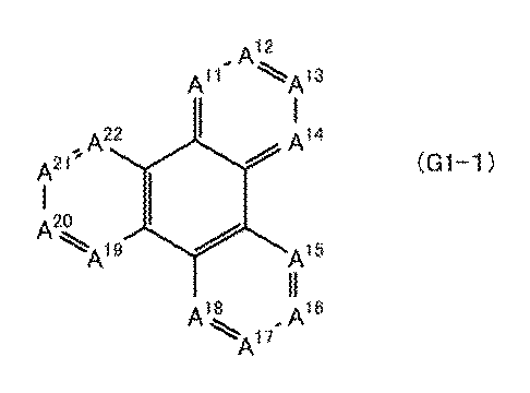
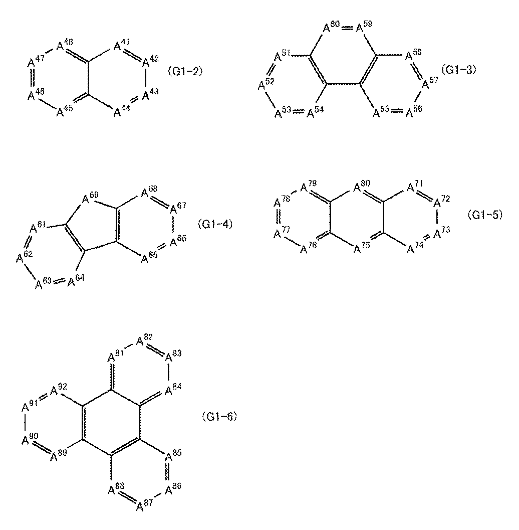

図2A乃至図2Dは、実施の形態に係る発光装置を説明する図である。
図3A乃至図3Cは、実施の形態に係る発光装置の製造方法を説明する図である。
図4A乃至図4Cは、実施の形態に係る発光装置の製造方法を説明する図である。
図5A乃至図5Cは、実施の形態に係る発光装置の製造方法を説明する図である。
図6A乃至図6Dは、実施の形態に係る発光装置の製造方法を説明する図である。
図7A乃至図7Eは、実施の形態に係る発光装置を説明する図である。
図8A乃至図8Fは、実施の形態に係る装置および画素配置を説明する図である。
図9A乃至図9Cは、実施の形態に係る画素回路を説明する図である。
図10は、実施の形態に係る発光装置を説明する図である。
図11A乃至図11Eは、実施の形態に係る電子機器を説明する図である。
図12A乃至図12Eは、実施の形態に係る電子機器を説明する図である。
図13Aおよび図13Bは、実施の形態に係る電子機器を説明する図である。
図14Aおよび図14Bは、実施の形態に係る照明装置を説明する図である。
図15は、実施の形態に係る照明装置を説明する図である。
図16A乃至図16Cは実施の形態に係る発光デバイスおよび受光デバイスを説明する図である。
図17Aおよび図17Bは実施の形態に係る発光デバイスおよび受光デバイスを説明する図である。
図18Aおよび図18BはPn−mDBqPTznの1H−NMRスペクトルである。
図19はPn−mDBqPTznのジクロロメタン溶液における吸収スペクトルと発光スペクトルである。
図20はPn−mDBqPTznの薄膜の吸収スペクトルと発光スペクトルである。
図21は発光デバイス1および発光デバイス2の発光スペクトルである。
図22は発光デバイス1および発光デバイス2の外部量子効率−輝度特性である。
図23は発光デバイス1および発光デバイス2の電流−電圧特性である。
図24は、室温において、発光デバイス1および発光デバイス2の駆動時間に対する輝度の変化を表す図である。
図25は、85℃において、発光デバイス1および発光デバイス2の駆動時間に対する輝度変化を表す図である。
本実施の形態では、本発明の一態様の有機化合物(本願化合物ともいう)について説明する。本発明の一態様の化合物は、アジン骨格を有する有機化合物(アジン化合物ともいう)である。アジン骨格とは、ベンゼン環の一つ以上の炭素が窒素に置換した骨格を指し、一例としてピリジン骨格、ピラジン骨格、ピリミジン骨格、ピリダジン骨格、またはトリアジン骨格などが上げられる。アジン骨格を有する化合物は、例えば、下記一般式(G1)で表される有機化合物である。


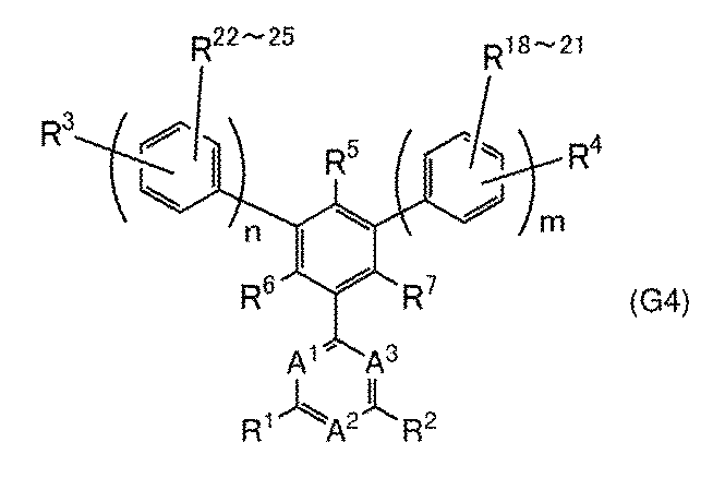


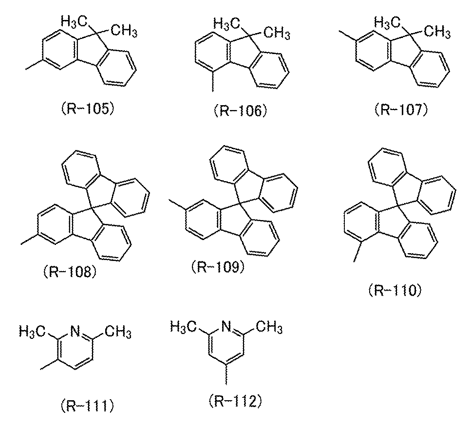

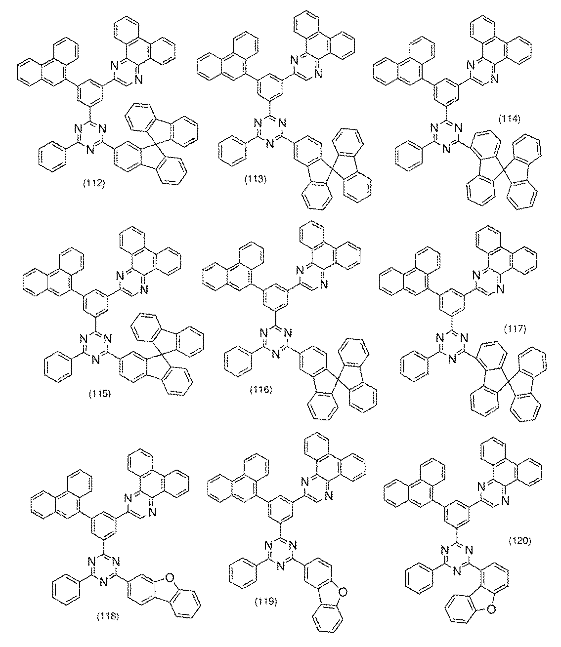


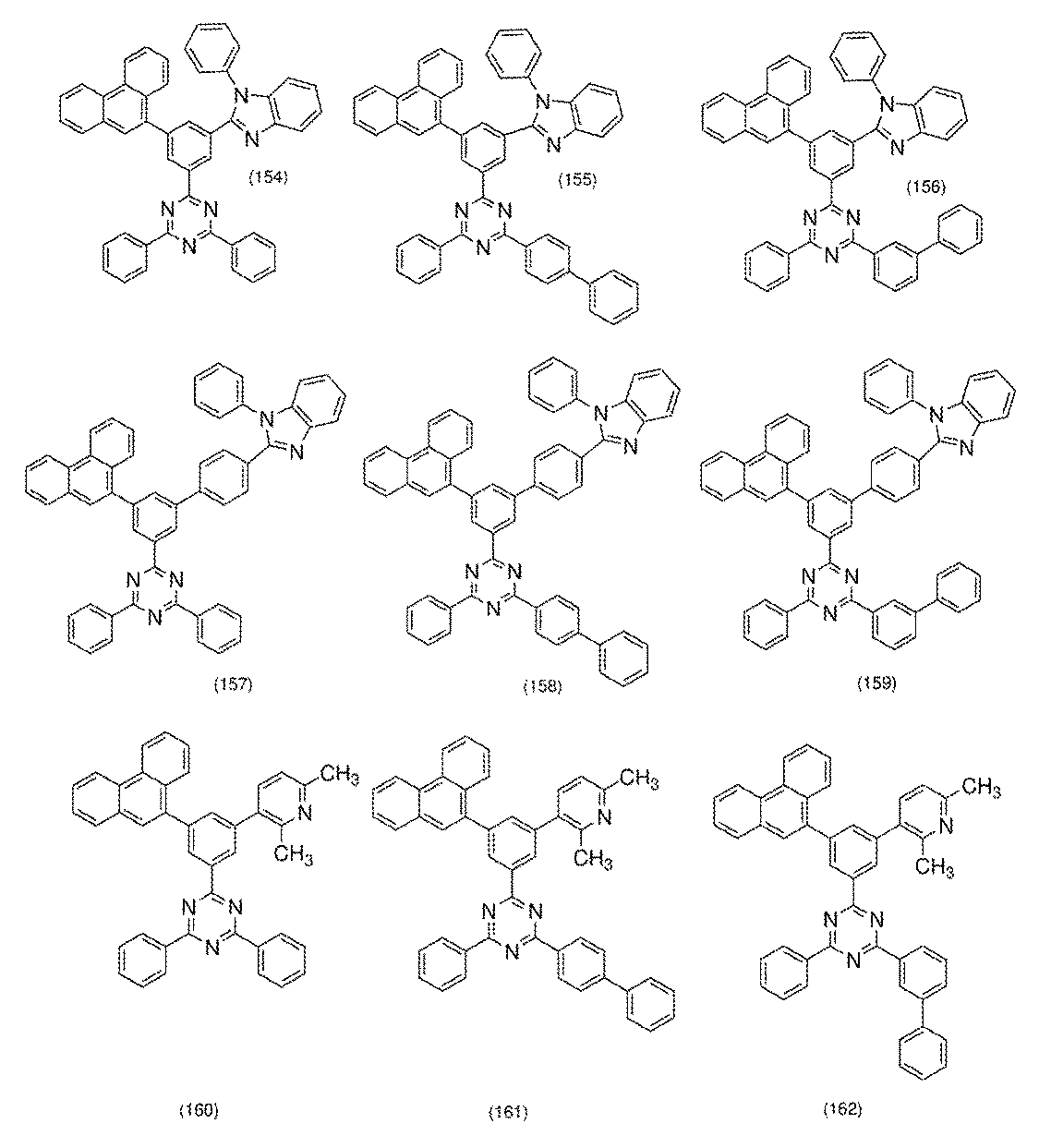
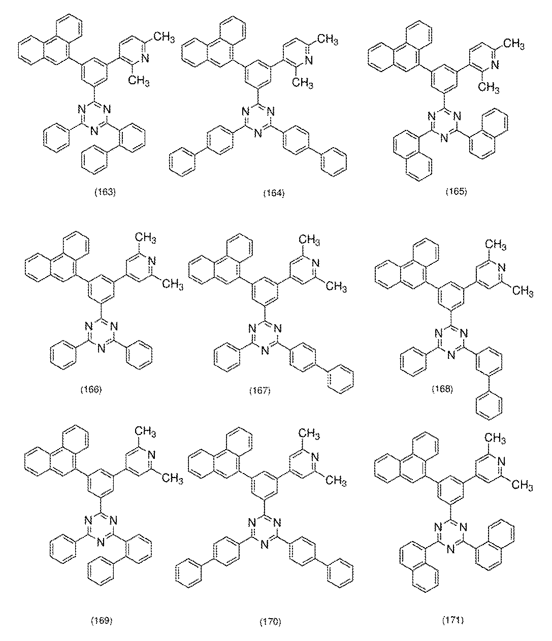
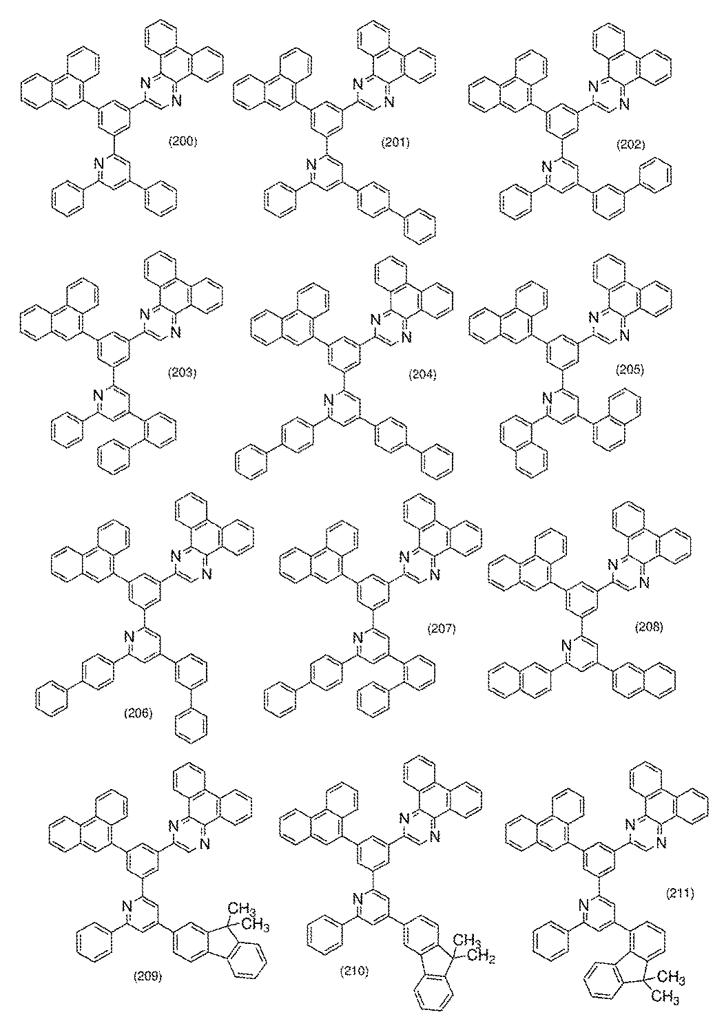


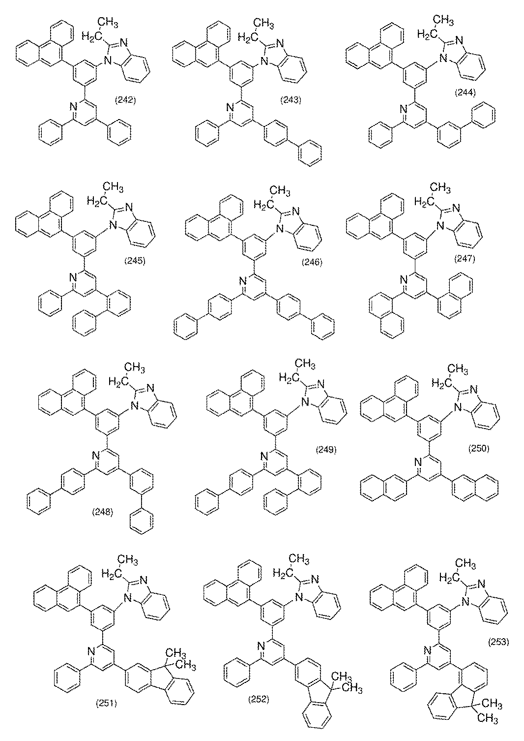
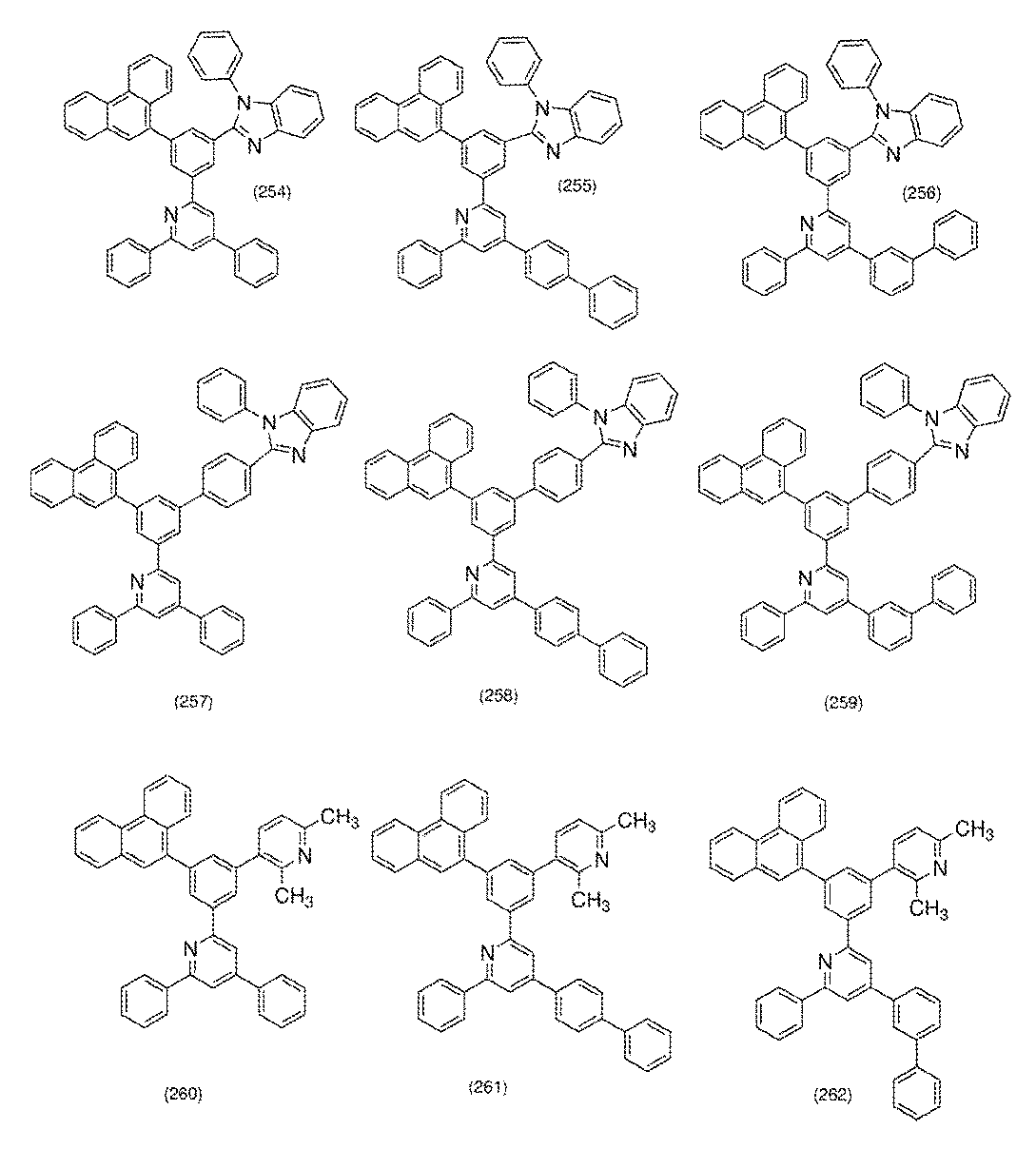
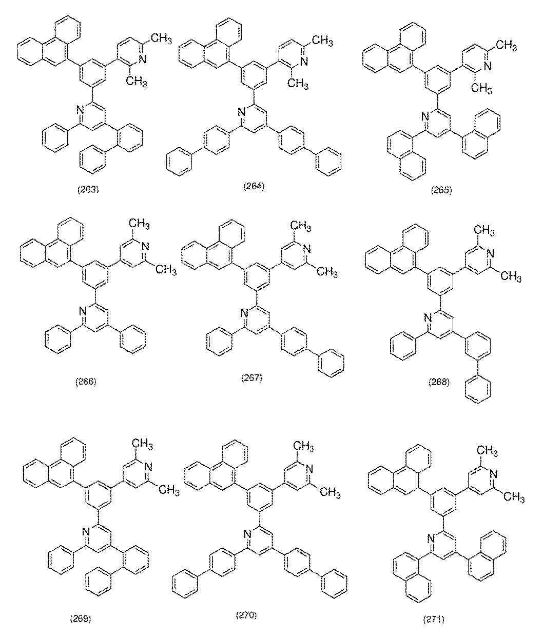

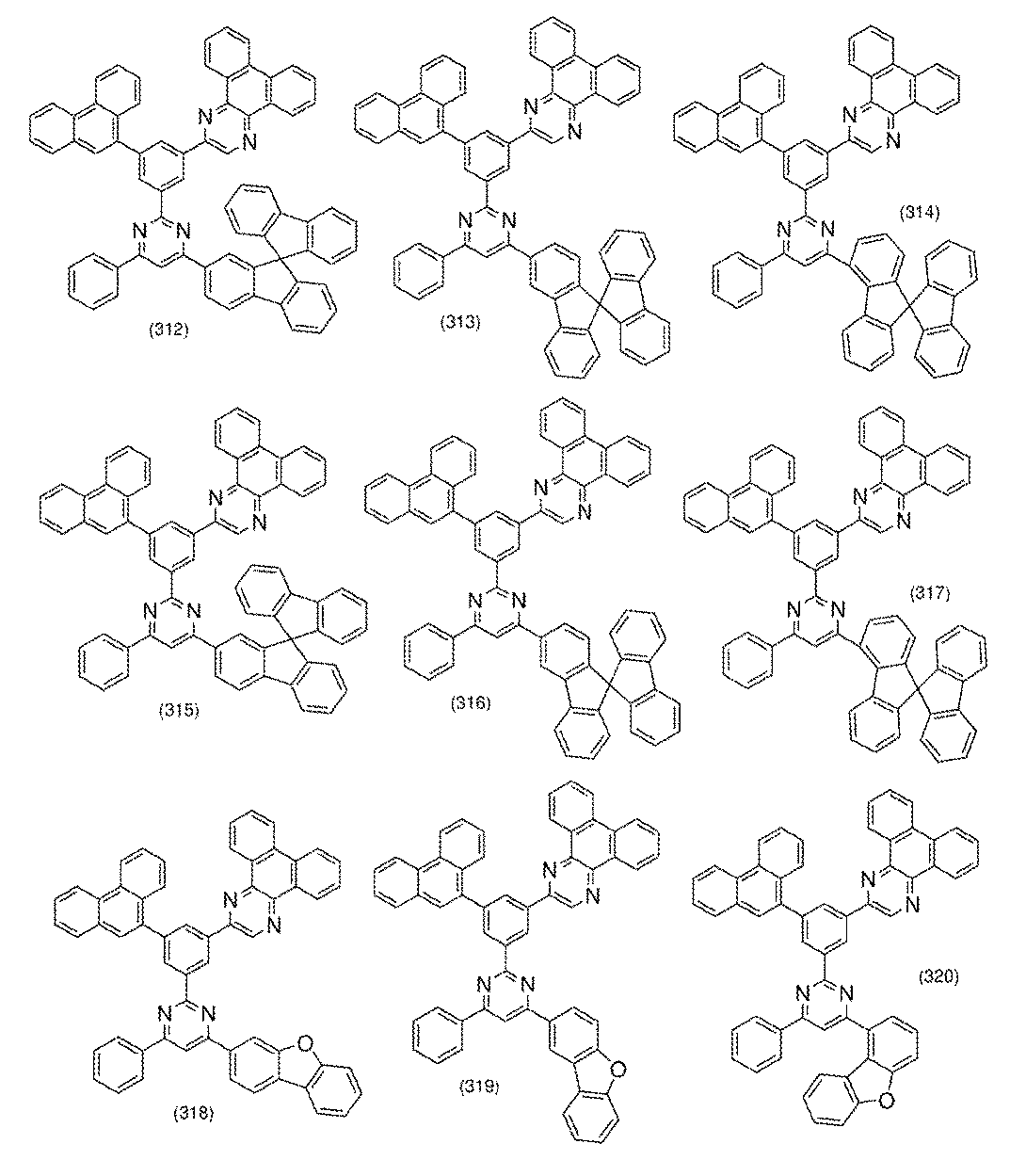

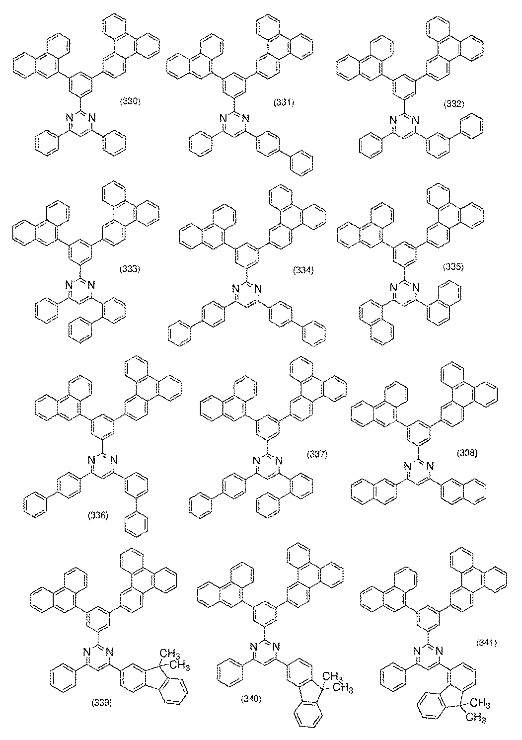


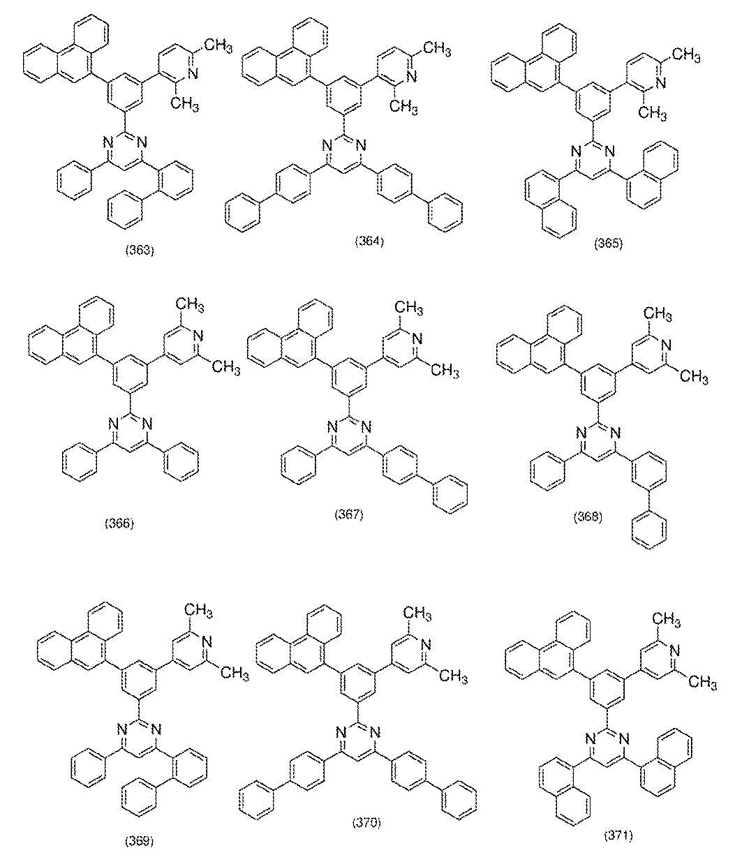
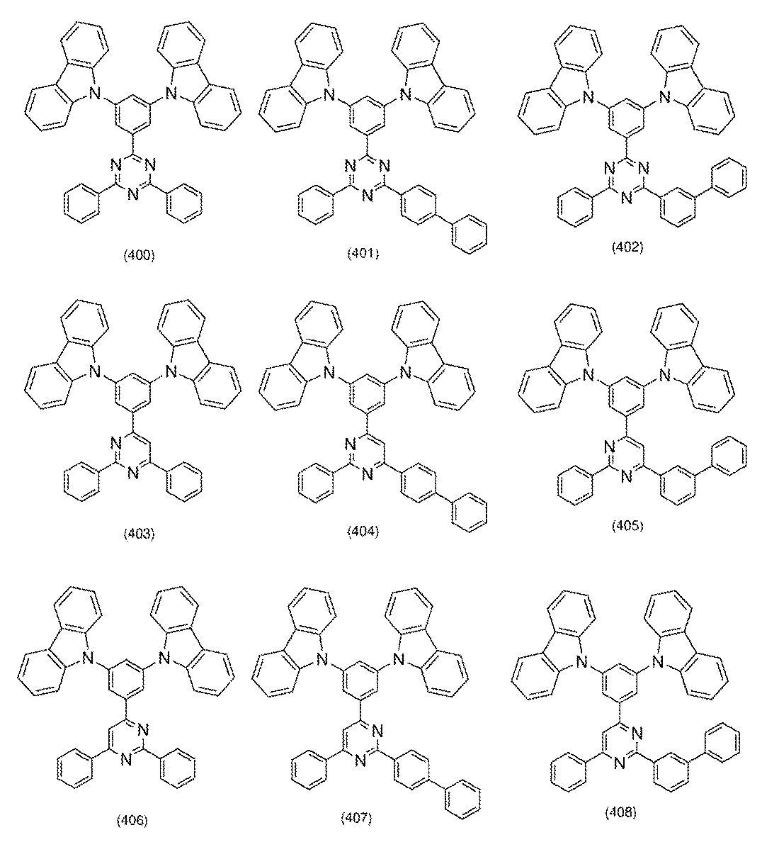
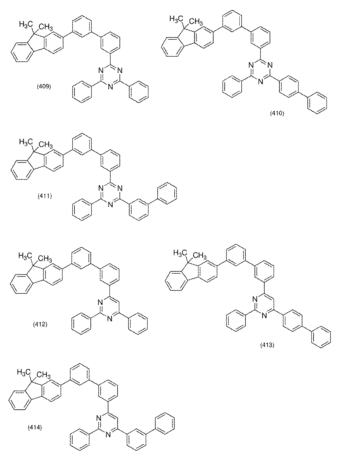


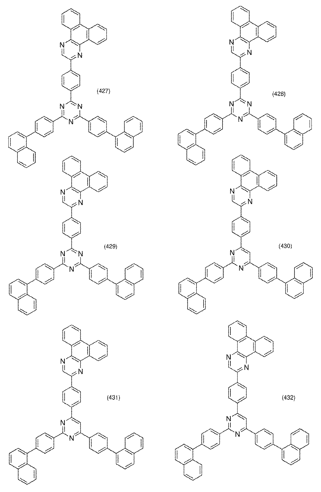
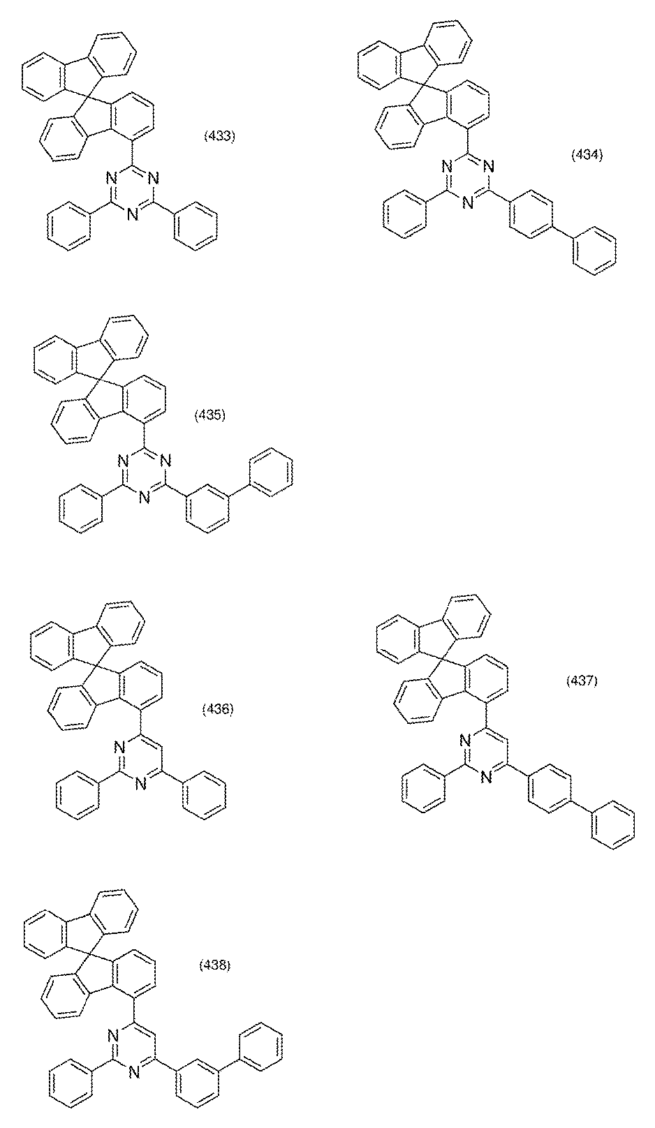
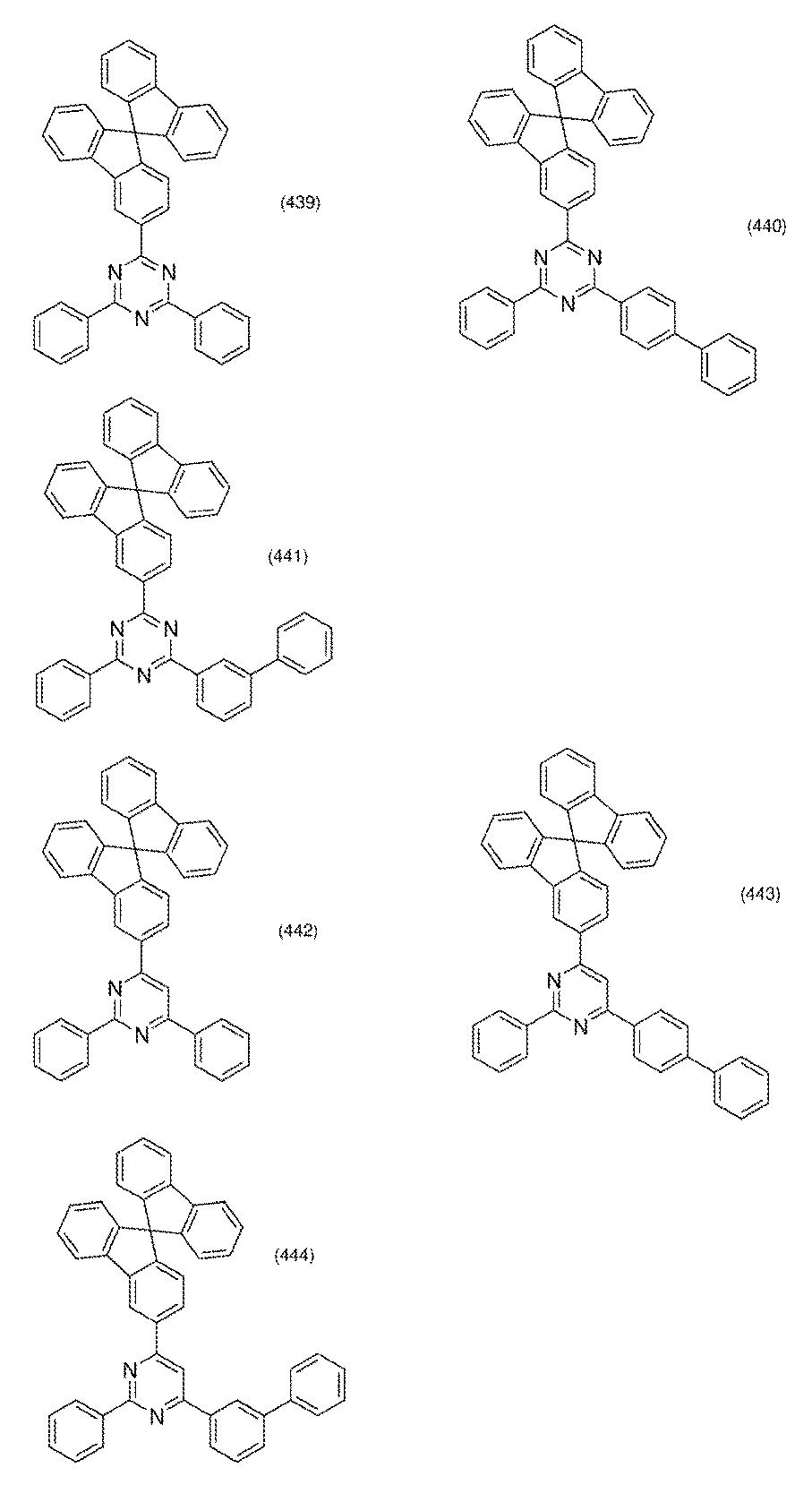
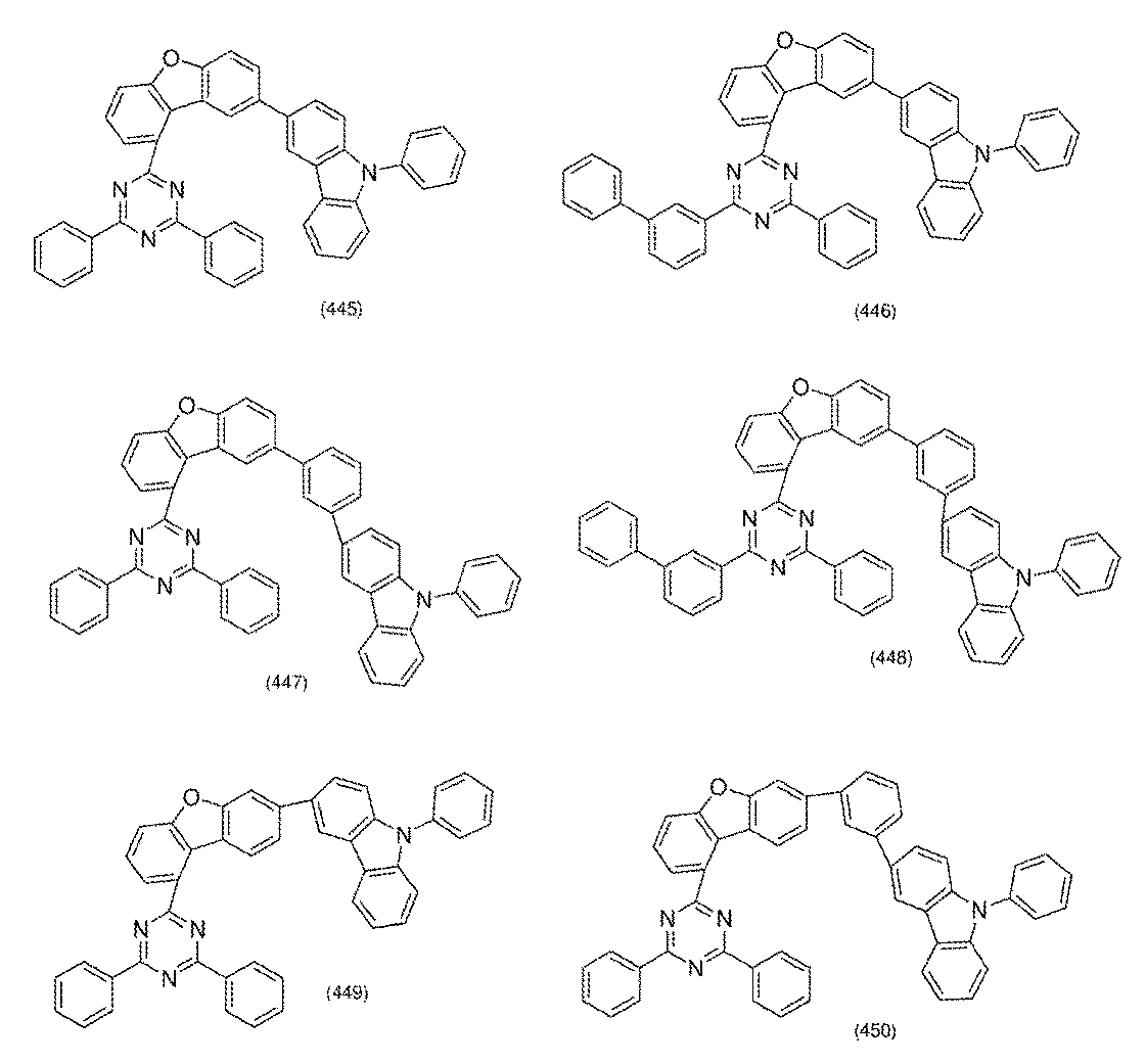
本実施の形態では、下記一般式(G1)で表される有機化合物の合成方法について説明する。
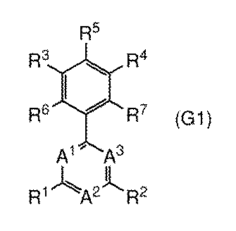

本実施の形態では、実施の形態1で示した有機化合物を用いた発光デバイスの構成について、図1A乃至図1Eを用いて説明する。
発光デバイスの基本的な構造について説明する。図1Aには、一対の電極間に発光層を含むEL層を有する発光デバイスを示す。具体的には、第1の電極101と第2の電極102との間にEL層103が挟まれた構造を有する。
次に、本発明の一態様である発光デバイスの具体的な構造について説明する。また、ここでは、タンデム構造を有する図1Dを用いて説明する。なお、図1Aおよび図1Cに示すシングル構造の発光デバイスについてもEL層の構成については同様とする。また、図1Dに示す発光デバイスがマイクロキャビティ構造を有する場合は、第1の電極101を反射電極として形成し、第2の電極102を半透過・半反射電極として形成する。従って、所望の電極材料を単数または複数用い、単層または積層して形成することができる。なお、第2の電極102は、EL層103bを形成した後、適宜材料を選択して形成する。
第1の電極101および第2の電極102を形成する材料としては、上述した両電極の機能が満たせるのであれば、以下に示す材料を適宜組み合わせて用いることができる。例えば、金属、合金、電気伝導性化合物、およびこれらの混合物などを適宜用いることができる。具体的には、In−Sn酸化物(ITOともいう)、In−Si−Sn酸化物(ITSOともいう)、In−Zn酸化物、In−W−Zn酸化物が挙げられる。その他、アルミニウム(Al)、チタン(Ti)、クロム(Cr)、マンガン(Mn)、鉄(Fe)、コバルト(Co)、ニッケル(Ni)、銅(Cu)、ガリウム(Ga)、亜鉛(Zn)、インジウム(In)、スズ(Sn)、モリブデン(Mo)、タンタル(Ta)、タングステン(W)、パラジウム(Pd)、金(Au)、白金(Pt)、銀(Ag)、イットリウム(Y)、ネオジム(Nd)などの金属、およびこれらを適宜組み合わせて含む合金を用いることもできる。その他、上記例示のない元素周期表の第1族または第2族に属する元素(例えば、リチウム(Li)、セシウム(Cs)、カルシウム(Ca)、ストロンチウム(Sr))、ユウロピウム(Eu)、イッテルビウム(Yb)などの希土類金属およびこれらを適宜組み合わせて含む合金、その他グラフェン等を用いることができる。
正孔注入層(111、111a、111b)は、陽極である第1の電極101および電荷発生層(106、106a、106b)からEL層(103、103a、103b)に正孔(ホール)を注入する層であり、有機アクセプタ材料および正孔注入性の高い材料を含む層である。
正孔輸送層(112、112a、112b)は、正孔注入層(111、111a、111b)によって、第1の電極101から注入された正孔を発光層(113、113a、113b)に輸送する層である。なお、正孔輸送層(112、112a、112b)は、正孔輸送性材料を含む層である。従って、正孔輸送層(112、112a、112b)には、正孔注入層(111、111a、111b)に用いることができる正孔輸送性材料を用いることができる。
発光層(113、113a、113b、113c)は、発光物質を含む層である。なお、発光層(113、113a、113b、113c)に用いることができる発光物質としては、青色、紫色、青紫色、緑色、黄緑色、黄色、橙色、赤色などの発光色を呈する物質を適宜用いることができる。また、発光層を複数有する場合には、各発光層に異なる発光物質を用いることにより異なる発光色を呈する構成(例えば、補色の関係にある発光色を組み合わせて得られる白色発光)とすることができる。さらに、一つの発光層が異なる発光物質を有する積層構造としてもよい。
発光層(113、113a、113b、113c)に用いることのできる、一重項励起エネルギーを発光に変える発光物質としては、以下に示す蛍光を発する物質(蛍光発光物質)が挙げられる。例えば、ピレン誘導体、アントラセン誘導体、トリフェニレン誘導体、フルオレン誘導体、カルバゾール誘導体、ジベンゾチオフェン誘導体、ジベンゾフラン誘導体、ジベンゾキノキサリン誘導体、キノキサリン誘導体、ピリジン誘導体、ピリミジン誘導体、フェナントレン誘導体、ナフタレン誘導体などが挙げられる。特にピレン誘導体は発光量子収率が高いので好ましい。ピレン誘導体の具体例としては、N,N’−ビス(3−メチルフェニル)−N,N’−ビス[3−(9−フェニル−9H−フルオレン−9−イル)フェニル]ピレン−1,6−ジアミン(略称:1,6mMemFLPAPrn)、N,N’−ジフェニル−N,N’−ビス[4−(9−フェニル−9H−フルオレン−9−イル)フェニル]ピレン−1,6−ジアミン(略称:1,6FLPAPrn)、N,N’−ビス(ジベンゾフラン−2−イル)−N,N’−ジフェニルピレン−1,6−ジアミン(略称:1,6FrAPrn)、N,N’−ビス(ジベンゾチオフェン−2−イル)−N,N’−ジフェニルピレン−1,6−ジアミン(略称:1,6ThAPrn)、N,N’−(ピレン−1,6−ジイル)ビス[(N−フェニルベンゾ[b]ナフト[1,2−d]フラン)−6−アミン](略称:1,6BnfAPrn)、N,N’−(ピレン−1,6−ジイル)ビス[(N−フェニルベンゾ[b]ナフト[1,2−d]フラン)−8−アミン](略称:1,6BnfAPrn−02)、N,N’−(ピレン−1,6−ジイル)ビス[(6,N−ジフェニルベンゾ[b]ナフト[1,2−d]フラン)−8−アミン](略称:1,6BnfAPrn−03)などが挙げられる。
次に、発光層113に用いることのできる、三重項励起エネルギーを発光に変える発光物質としては、例えば、燐光を発する物質(燐光発光物質)、または熱活性化遅延蛍光を示す熱活性化遅延蛍光(Thermally activated delayed fluorescence:TADF)材料が挙げられる。
青色または緑色を呈し、発光スペクトルのピーク波長が450nm以上570nm以下である燐光発光物質としては、以下のような物質が挙げられる。
緑色または黄色を呈し、発光スペクトルのピーク波長が495nm以上590nm以下である燐光発光物質としては、以下のような物質が挙げられる。
黄色または赤色を呈し、発光スペクトルのピーク波長が570nm以上750nm以下である燐光発光物質としては、以下のような物質が挙げられる。
また、TADF材料としては、以下に示す材料を用いることができる。TADF材料とは、S1準位とT1準位との差が小さく(好ましくは、0.2eV以下)、三重項励起状態をわずかな熱エネルギーによって一重項励起状態にアップコンバート(逆項間交差)が可能で、一重項励起状態からの発光(蛍光)を効率よく呈する材料のことである。また、熱活性化遅延蛍光が効率良く得られる条件としては、三重項励起エネルギー準位と一重項励起エネルギー準位のエネルギー差が0eV以上0.2eV以下、好ましくは0eV以上0.1eV以下であることが挙げられる。また、TADF材料における遅延蛍光とは、通常の蛍光と同様のスペクトルを持ちながら、寿命が著しく長い発光をいう。その寿命は、1×10⁻⁶秒以上、または1×10⁻³秒以上である。また、実施の形態1で説明した有機化合物を用いることができる。
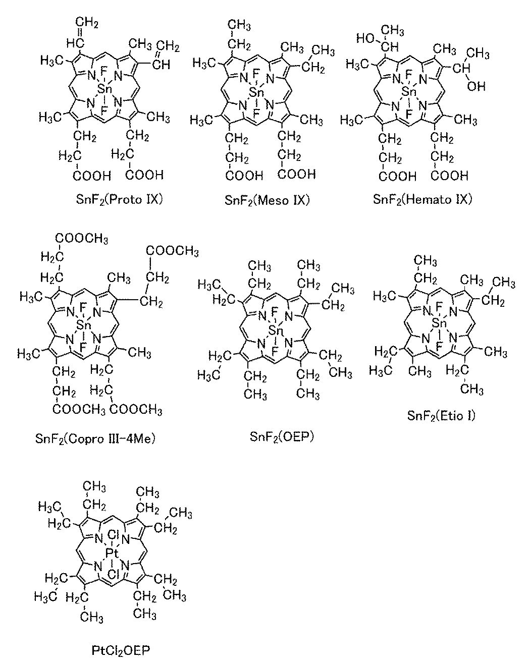
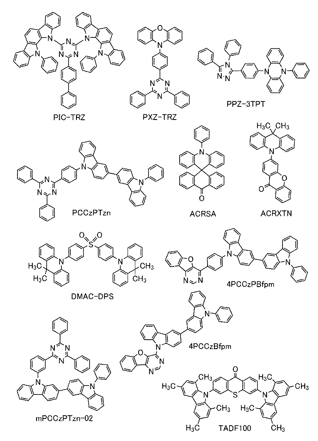
発光層(113、113a、113b、113c)に用いる発光物質が蛍光発光物質である場合、組み合わせる有機化合物(ホスト材料)として、一重項励起状態のエネルギー準位が大きく、三重項励起状態のエネルギー準位が小さい有機化合物、または蛍光量子収率が高い有機化合物を用いるのが好ましい。したがって、このような条件を満たす有機化合物であれば、本実施の形態で示す、正孔輸送性材料(前述)および電子輸送性材料(後述)等を用いることができる。また、実施の形態1で説明した有機化合物を用いることができる。
また、発光層(113、113a、113b、113c)に用いる発光物質が燐光発光物質である場合、組み合わせる有機化合物(ホスト材料)として、発光物質の三重項励起エネルギー(基底状態と三重項励起状態とのエネルギー差)よりも三重項励起エネルギーの大きい有機化合物を選択すれば良い。なお、励起錯体を形成させるべく複数の有機化合物(例えば、第1のホスト材料、および第2のホスト材料(またはアシスト材料)等)を発光物質と組み合わせて用いる場合は、これらの複数の有機化合物を燐光発光物質と混合して用いることが好ましい。また、実施の形態1で説明した有機化合物を用いることができる。
電子輸送層(114、114a、114b)は、後述する電子注入層(115、115a、115b)によって第2の電極102および電荷発生層(106、106a、106b)から注入された電子を発光層(113、113a、113b、113c)に輸送する層である。なお、本発明の一態様である発光デバイスは、電子輸送層が積層構造を有することで耐熱性を向上させることができる。また、電子輸送層(114、114a、114b)に用いる電子輸送性材料は、電界強度[V/cm]の平方根が600における電子移動度が、1×10−6cm2/Vs以上の電子移動度を有する物質が好ましい。なお、正孔よりも電子の輸送性の高い物質であれば、これら以外のものを用いることができる。また、電子輸送層(114、114a、114b)は、単層でも機能するが、2層以上の積層構造としてもよい。なお、上記の混合材料は、耐熱性を有するため、これを用いた電子輸送層上でフォトリソ工程を行うことにより、熱工程によるデバイス特性への影響を抑制することができる。
電子輸送層(114、114a、114b)に用いることができる電子輸送性材料としては、電子輸送性の高い有機化合物を用いることができ、例えば複素芳香族化合物を用いることができる。なお、複素芳香族化合物とは、環の中に少なくとも2種類の異なる元素を含む環式化合物である。なお、環構造としては、3員環、4員環、5員環、6員環等が含まれるが、特に5員環、または、6員環が好ましく、含まれる元素としては、炭素の他に窒素、酸素、または硫黄などのいずれか一又は複数を含む複素芳香族化合物が好ましい。特に窒素を含む複素芳香族化合物(含窒素複素芳香族化合物)が好ましく、含窒素複素芳香族化合物、またはこれを含むπ電子不足型複素芳香族化合物等の電子輸送性の高い材料(電子輸送性材料)を用いることが好ましい。実施の形態1の化合物は電子輸送性を有するため、電子輸送性材料として用いることができる。また、電子輸送層114aと電子輸送層114bとの両方に本願化合物を用いると更に好適である。
電子注入層(115、115a、115b)は、電子注入性の高い物質を含む層である。また、電子注入層(115、115a、115b)は、第2の電極102からの電子の注入効率を高めるための層であり、第2の電極102に用いる材料の仕事関数の値と、電子注入層(115、115a、115b)に用いる材料のLUMO準位の値とを比較した際、その差が小さい(0.5eV以下)材料を用いることが好ましい。従って、電子注入層115には、リチウム、セシウム、フッ化リチウム(LiF)、フッ化セシウム(CsF)、フッ化カルシウム(CaF2)、Liq、2−(2−ピリジル)フェノラトリチウム(略称:LiPP)、2−(2−ピリジル)−3−ピリジノラトリチウム(略称:LiPPy)、4−フェニル−2−(2−ピリジル)フェノラトリチウム(略称:LiPPP)リチウム酸化物(LiOx)、炭酸セシウム等のようなアルカリ金属、アルカリ土類金属、またはこれらの化合物を用いることができる。また、フッ化エルビウム(ErF3)、イッテルビウム(Yb)のような希土類金属または希土類金属化合物を用いることができる。なお、電子注入層(115、115a、115b)には、上記の材料を複数種混合して形成しても良いし、上記の材料のうち複数種を積層させて形成しても良い。また、電子注入層(115、115a、115b)にエレクトライドを用いてもよい。エレクトライドとしては、例えば、カルシウムとアルミニウムの混合酸化物に電子を高濃度添加した物質等が挙げられる。なお、上述した電子輸送層(114、114a、114b)を構成する物質を用いることもできる。本願化合物は、電子注入性に優れているため、電子注入層に用いると好適である。電子注入層115aと電子注入層115bの両方に本願化合物を用いると更に好適である。
電荷発生層106は、第1の電極(陽極)101と第2の電極(陰極)102との間に電圧を印加したときに、EL層103aに電子を注入し、EL層103bに正孔を注入する機能を有する。なお、電荷発生層106は、正孔輸送性材料に電子受容体(アクセプタ)が添加された構成(P型層ともいう)であっても、電子輸送性材料に電子供与体(ドナー)が添加された構成(電子注入バッファ層ともいう)であってもよい。また、これらの両方の構成が積層されていても良い。さらに、P型層と電子注入バッファ層との間に電子リレー層が設けられていても良い。なお、上述した材料を用いて電荷発生層106を形成することにより、EL層が積層された場合における駆動電圧の上昇を抑制することができる。本願化合物は、輸送性に優れているため、電荷発生層106に適用すると好適である。
なお、図1A乃至図1Eでは図示しないが、発光デバイスの第2の電極102上にキャップ層を設けてもよい。キャップ層には、例えば、屈折率の高い材料を用いることができる。キャップ層を第2の電極102上に設けることによって、第2の電極102から射出される光の取り出し効率を向上させることができる。キャップ層材料の屈折率は、電子輸送層材料の屈折率より高いことが好ましい。また、キャップ層材料の屈折率は、電子輸送層材料の屈折率よりも高く、かつ、発光層のホスト材料の屈折率よりも高く、かつ、正孔輸送層材料の屈折率よりも高いことが好ましい。また、キャップ層は積層構造でも良い。その場合、本願化合物を有する層と、その上層に本願化合物よりも屈折率の高い材料を有する層と、を積層することが好ましい。
本実施の形態で示した発光デバイスは、様々な基板上に形成することができる。なお、基板の種類は、特定のものに限定されることはない。基板の一例としては、半導体基板(例えば単結晶基板又はシリコン基板)、SOI基板、ガラス基板、石英基板、プラスチック基板、金属基板、ステンレス・スチル基板、ステンレス・スチル・ホイルを有する基板、タングステン基板、タングステン・ホイルを有する基板、可撓性基板、貼り合わせフィルム、繊維状の材料を含む紙、又は基材フィルムなどが挙げられる。
本実施の形態では、本発明の一態様である受発光装置の具体的な構成例、および製造方法の一例として、受発光装置700について説明する。なお、受発光装置700は、発光デバイスを有することから、発光装置ということもでき、受光デバイスを有することから、受光装置ということもでき、電子機器などの表示部に適用可能であることから、表示パネルまたは表示装置ということもできる。
図2Aに示す受発光装置700は、発光デバイス550B、発光デバイス550G、発光デバイス550R、および受光デバイス550PSを有する。また、発光デバイス550B、発光デバイス550G、発光デバイス550R、および受光デバイス550PSは、第1の基板510上に設けられた機能層520上に形成される。機能層520には、複数のトランジスタで構成されたゲートドライバ、ソースドライバなどの駆動回路の他、これらを電気的に接続する配線等が含まれる。なお、これらの駆動回路は、一例として、発光デバイス550B、発光デバイス550G、発光デバイス550R、および受光デバイス550PSと、それぞれ電気的に接続され、これらを駆動することができる。また、受発光装置700は、機能層520および各デバイス(発光デバイスおよび受光デバイス)上に絶縁層705を備え、絶縁層705は、第2の基板770と機能層520とを貼り合わせる機能を有する。
図3Aに示すように、電極551B、電極551G、電極551R、および電極551PSを形成する。例えば、第1の基板510上に形成された機能層520上に導電膜を形成し、フォトリソグラフィ法を用いて、所定の形状に加工する。
本実施の形態では、装置720について、図8乃至図10を用いて説明する。なお、図8乃至図10に示す装置720は、実施の形態2で示す発光デバイスを有することから発光装置であるが、本実施の形態で説明する装置720は、電子機器などの表示部に適用可能であることから表示パネルまたは表示装置ということもできる。また、上記発光デバイスを光源とし、発光デバイスからの光を受光できる受光デバイスを備える構成とする場合には、受発光装置ということもできる。なお、これらの発光装置、表示パネル、表示装置、および受発光装置は、少なくとも発光デバイスを有する構成とする。
本実施の形態では、本発明の一態様の電子機器の構成について、図11A乃至図13Bにより説明する。
本実施の形態では、実施の形態2に記載の発光デバイスを照明装置として用いる構成について、図14により説明する。なお、図14Aは、図14Bに示す照明装置の上面図における線分e−fの断面図である。
本実施の形態では、本発明の一態様である発光装置、またはその一部である発光デバイスを適用して作製される照明装置の応用例について、図15を用いて説明する。
本実施の形態では、本発明の一態様である発光装置に適用できる、発光デバイスおよび受光デバイスの一例として、図16に示した受発光装置810について説明する。なお、受発光装置810は、発光デバイスを有することから、発光装置ということもでき、受光デバイスを有することから、受光装置ということもでき、電子機器などの表示部に適用可能であることから、表示パネルまたは表示装置ということもできる。
本合成例では、実施の形態1において構造式(100)として示した、2−[3−(ジベンゾ[f,h]キノキサリン−2−イル)−5−(9−フェナントレン−9−イル)フェニル]−4,6−ジフェニル−1,3,5−トリアジン(略称:Pn−mDBqPTzn)の合成方法について具体的に説明する。

ステップ1は以下の手順にて行った。合成スキームは式(A−1)に示す。

ステップ2は以下の手順にて行った。合成スキームは式(A−2)に示す。

ステップ3は以下の手順にて行った。合成スキームは式(A−2)に示す。
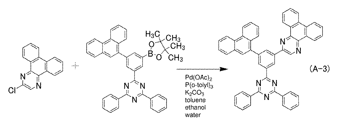
得られた白色固体2.0gをトレインサブリメーション法により圧力2.8Pa、アルゴン流量15mL/min、360℃の条件で14時間加熱し、昇華精製して白色固体1.0g(回収率50%)を得た。
Pn−mDBqPTznの吸収スペクトルおよび発光スペクトルを測定した。吸収スペクトルの測定には、紫外可視分光光度計((株)日立製 U−4100)を用いた。また、発光スペクトルの測定には、蛍光光度計((株)日本分光製 FP−8600)を用いた。
Pn−mDBqPTznのガラス転移温度(Tg)を測定した。Tgは、示差走査熱量測定装置((株)パーキンエルマージャパン製、PYRIS1DSC)を用い、アルミセルに粉末を乗せ、測定した。この結果、Pn−mDBqPTznのTgは161℃であった。このことから本発明の化合物は非常に高い熱物性を示すことが明らかとなり、このような化合物を用いて作製した薄膜は膜質が安定であることが期待できる。膜質が安定した薄膜を形成できる化合物を有機デバイスに用いることで高い耐熱性を有する有機デバイスを提供する事が可能となる。
また、Pn−mDBqPTznのHOMO準位およびLUMO準位をサイクリックボルタンメトリ(CV)測定を元に算出した。算出方法を以下に示す。
Pn−mDBqPTznの屈折率を分光エリプソメーター(ジェー・エー・ウーラム・ジャパン社製M−2000U)を用いて測定した。測定には、石英基板上にPn−mDBqPTznを真空蒸着法により約50nm成膜した膜を使用した。波長633nmおいて、常光線の屈折率であるnOrdinary(nO)は1.85であった。この結果、Pn−mDBqPTzn、ホスト材料、ホール輸送性材料、電子輸送性材料、または陰極上に設けられるキャップ層材料としても有効に利用可能であることがわかった。キャップ層材料として用いる場合、屈折率が1.75以上2.50以下であることが好ましい。
本合成例では、有機デバイスを構成し得る材料(例えば、電子輸送性材料およびホスト材料等)として利用可能な有機化合物であって、構造式(160)として示した、2−[3−(2,6−ジメチル−3−ピリジニル)−5−(9−フェナントレニル)フェニル]−4,6−ジフェニル−1,3,5−トリアジン(略称:mPn−mDMePyPTzn)の合成方法について説明する。
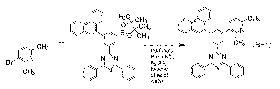
本合成例では、有機デバイスを構成し得る材料(例えば、電子輸送性材料およびホスト材料等)として利用可能な有機化合物であって、構造式(440)として示した、2−[(1,1’−ビフェニル)−4−イル]−4−フェニル−6−[9,9’−スピロビ(9H−フルオレン)−2−イル]−1,3,5−トリアジン(略称:BP−SFTzn)の合成方法について説明する。合成スキームは式(C−1)に示した。

本合成例では、有機デバイスを構成し得る材料(例えば、電子輸送性材料およびホスト材料等)として利用可能な有機化合物であって、構造式(434)として示した、2−[(1,1’−ビフェニル)−4−イル]−4−フェニル−6−{(3’,5’−ジ−tert−ブチル)−1,1’−ビフェニル−3−イル}−1,3,5−トリアジン(略称:BP−SF(4)Tzn)の合成方法について説明する。
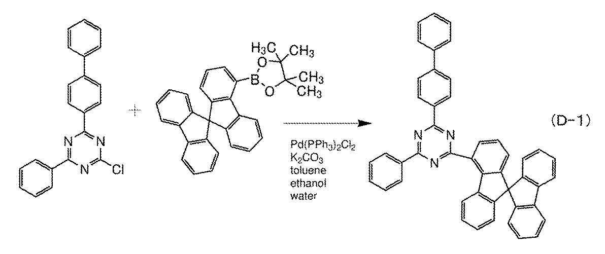
本合成例では、有機デバイスを構成し得る材料(例えば、電子輸送性材料およびホスト材料等)として利用可能な有機化合物であって、構造式(424)として示した、2,4−ビス[4−(1−ナフチル)フェニル]−6−[4−(3−ピリジル)フェニル]ピリミジン(略称:2,4NP−6PyPPm)の合成方法について説明する。

本合成例では、有機デバイスを構成し得る材料(例えば、電子輸送性材料およびホスト材料等)として利用可能な有機化合物であって、構造式(404)として示した、4−[3,5−ビス(9H−カルバゾール−9−イル)フェニル]−2−フェニル−6−(1,1’−ビフェニル−4−イル)ピリミジン(略称:6BP−4Cz2PPm)の合成方法について説明する。

本合成例では、有機デバイスを構成し得る材料(例えば、電子輸送性材料およびホスト材料等)として利用可能な有機化合物であって、構造式(405)として示した、6−(1,1’−ビフェニル−3−イル)−4−[3,5−ビス(9H−カルバゾール−9−イル)フェニル]−2−フェニルピリミジン(略称:6mBP−4Cz2PPm)の合成方法について説明する。
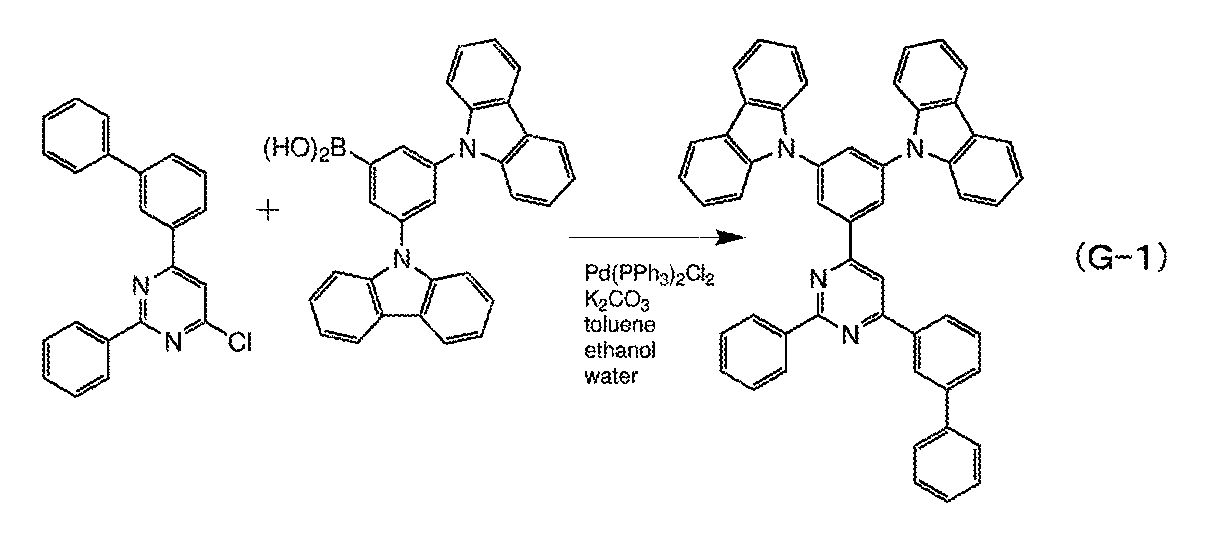
本合成例では、有機デバイスを構成し得る材料(例えば、電子輸送性材料およびホスト材料等)として利用可能な有機化合物であって、構造式(409)として示した、2−[3’−(9,9−ジメチル−9H−フルオレン−2−イル)ビフェニル−3−イル]−4,6−ジフェニル−1,3,5−トリアジン(略称:mFBPTzn)の合成方法について説明する。

本合成例では、有機デバイスを構成し得る材料(例えば、電子輸送性材料およびホスト材料等)として利用可能な有機化合物であって、構造式(445)として示した、3−[9−(4,6−ジフェニル−1,3,5−トリアジン−2−イル)−2−ジベンゾフラニル]−9−フェニル−9H−カルバゾール(略称:PCDBfTzn)の合成方法について説明する。
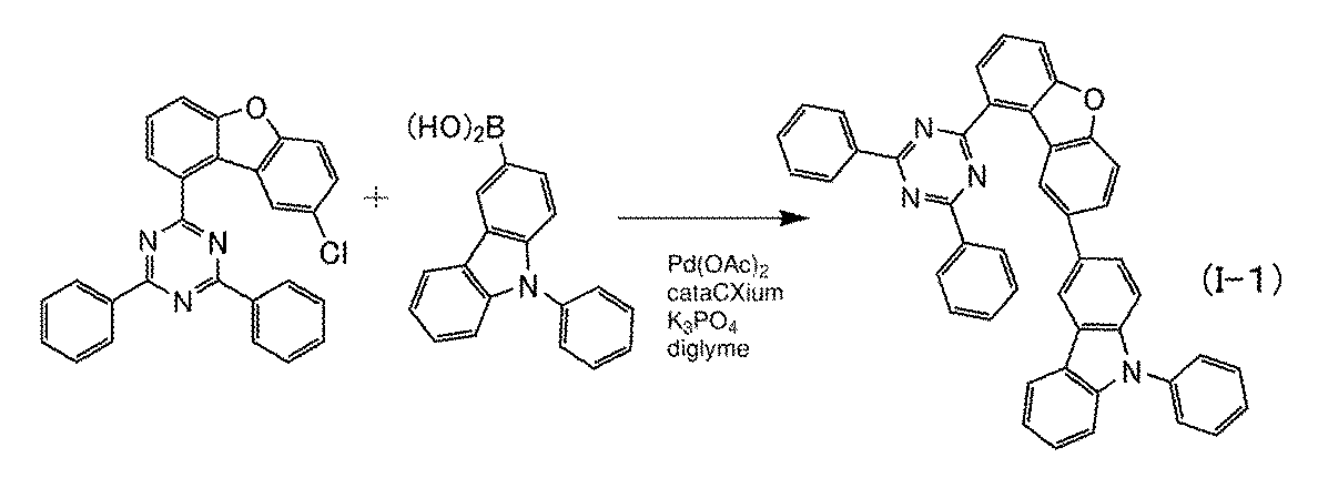
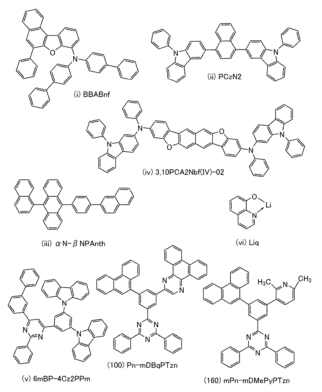
まず、ガラス基板上に、酸化珪素を含むインジウム錫酸化物(ITSO)をスパッタリング法にて成膜し、第1の電極を形成した。なお、その膜厚は70nmとし、電極面積は2mm×2mmとした。
発光デバイス2は、上記発光デバイス1の第2の電子輸送層におけるPn−mDBqPTznに変えて、本発明の一態様であるmPn−mDMePyPTzn(構造式(160))を用いたものである。


Claims (10)
- 一般式(G1)で表される有機化合物。

- 一般式(G1)中、前記R3は一般式(G1−1)を表し、前記R4は一般式(G1−2)乃至一般式(G1−6)のいずれか一を表す請求項1の有機化合物。
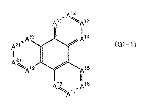

- 一般式(G1)中、前記R1および前記R2は、置換又は無置換のフェニル基である請求項1乃至請求項2のいずれか一の有機化合物。
- 一般式(G1)で表され、ガラス転移温度が150℃以上である、請求項1乃至請求項3のいずれか一の有機化合物。
- 一般式(G1)中、前記R3および前記R4は、分子量が150以上である請求項1乃至請求項4のいずれか一の有機化合物。
- 式(100)で表される有機化合物。
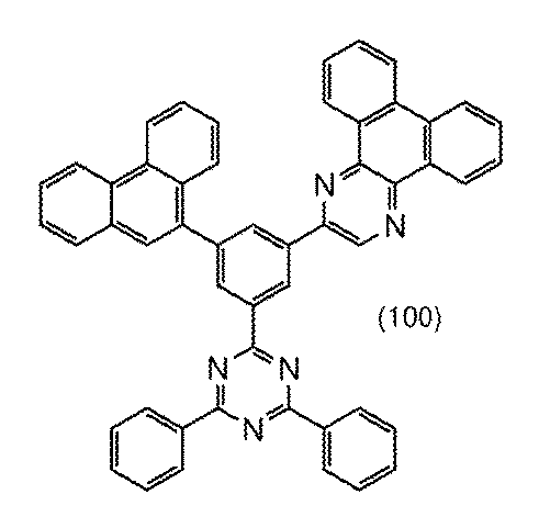
- 請求項1乃至請求項6のいずれか一の化合物を含む有機デバイス。
- 請求項1乃至請求項6のいずれか一の化合物を含む電子機器。
- 請求項7に記載の有機デバイスと、トランジスタ、または、基板と、を有する発光装置。
- 請求項9に記載の発光装置と、センサ、操作ボタン、スピーカ、または、マイクと、を有する電子機器。
Priority Applications (2)
| Application Number | Priority Date | Filing Date | Title |
|---|---|---|---|
| JP2023564272A JPWO2023100019A5 (ja) | 2022-11-18 | 発光デバイス | |
| US18/710,010 US20250042877A1 (en) | 2021-11-30 | 2022-11-18 | Organic compound, organic device, light-emitting apparatus, and electronic appliance |
Applications Claiming Priority (2)
| Application Number | Priority Date | Filing Date | Title |
|---|---|---|---|
| JP2021194181 | 2021-11-30 | ||
| JP2021-194181 | 2021-11-30 |
Publications (1)
| Publication Number | Publication Date |
|---|---|
| WO2023100019A1 true WO2023100019A1 (ja) | 2023-06-08 |
Family
ID=86611609
Family Applications (1)
| Application Number | Title | Priority Date | Filing Date |
|---|---|---|---|
| PCT/IB2022/061119 Ceased WO2023100019A1 (ja) | 2021-11-30 | 2022-11-18 | 有機化合物、有機デバイス、発光装置および電子機器 |
Country Status (2)
| Country | Link |
|---|---|
| US (1) | US20250042877A1 (ja) |
| WO (1) | WO2023100019A1 (ja) |
Citations (5)
| Publication number | Priority date | Publication date | Assignee | Title |
|---|---|---|---|---|
| KR20150122343A (ko) * | 2014-04-23 | 2015-11-02 | 덕산네오룩스 주식회사 | 유기전기 소자용 화합물, 이를 이용한 유기전기소자 및 그 전자 장치 |
| CN109705148A (zh) * | 2018-12-28 | 2019-05-03 | 武汉天马微电子有限公司 | 芳香环化合物、显示面板以及显示装置 |
| CN112830900A (zh) * | 2021-01-07 | 2021-05-25 | 吉林奥来德光电材料股份有限公司 | 磷光化合物及其制备方法和包含它的有机电致发光器件 |
| KR20210105559A (ko) * | 2020-02-19 | 2021-08-27 | 덕산네오룩스 주식회사 | 유기전기소자용 화합물, 이를 이용한 유기전기소자 및 그 전자 장치 |
| US20210320259A1 (en) * | 2020-04-13 | 2021-10-14 | Samsung Display Co,.Ltd. | Heterocyclic compound and organic light-emitting device including heterocyclic compound |
-
2022
- 2022-11-18 US US18/710,010 patent/US20250042877A1/en active Pending
- 2022-11-18 WO PCT/IB2022/061119 patent/WO2023100019A1/ja not_active Ceased
Patent Citations (5)
| Publication number | Priority date | Publication date | Assignee | Title |
|---|---|---|---|---|
| KR20150122343A (ko) * | 2014-04-23 | 2015-11-02 | 덕산네오룩스 주식회사 | 유기전기 소자용 화합물, 이를 이용한 유기전기소자 및 그 전자 장치 |
| CN109705148A (zh) * | 2018-12-28 | 2019-05-03 | 武汉天马微电子有限公司 | 芳香环化合物、显示面板以及显示装置 |
| KR20210105559A (ko) * | 2020-02-19 | 2021-08-27 | 덕산네오룩스 주식회사 | 유기전기소자용 화합물, 이를 이용한 유기전기소자 및 그 전자 장치 |
| US20210320259A1 (en) * | 2020-04-13 | 2021-10-14 | Samsung Display Co,.Ltd. | Heterocyclic compound and organic light-emitting device including heterocyclic compound |
| CN112830900A (zh) * | 2021-01-07 | 2021-05-25 | 吉林奥来德光电材料股份有限公司 | 磷光化合物及其制备方法和包含它的有机电致发光器件 |
Also Published As
| Publication number | Publication date |
|---|---|
| US20250042877A1 (en) | 2025-02-06 |
| JPWO2023100019A1 (ja) | 2023-06-08 |
Similar Documents
| Publication | Publication Date | Title |
|---|---|---|
| JP2023016026A (ja) | 発光デバイス、発光装置、電子機器、および照明装置 | |
| JP2023133235A (ja) | 有機化合物、受光デバイス、受発光装置、および電子機器 | |
| JP2023007468A (ja) | 発光デバイスおよび発光装置 | |
| JP2023090678A (ja) | 有機化合物、発光デバイス、発光装置、電子機器、および照明装置 | |
| JP2022161853A (ja) | 有機化合物、発光デバイス、発光装置、電子機器および照明装置 | |
| WO2023094936A1 (ja) | 発光デバイス、発光装置、有機化合物、電子機器、および照明装置 | |
| JP2023035912A (ja) | 発光デバイス、発光装置、電子機器、および照明装置 | |
| JP2023029303A (ja) | 発光デバイス、発光装置、有機化合物、電子機器、および照明装置 | |
| JP2022159214A (ja) | 有機化合物、発光デバイス、発光装置、電子機器および照明装置 | |
| KR20240051163A (ko) | 수광 디바이스, 수발광 장치, 및 전자 기기 | |
| JP2022132168A (ja) | 混合材料 | |
| US20250042877A1 (en) | Organic compound, organic device, light-emitting apparatus, and electronic appliance | |
| US20260132134A1 (en) | Organic compound, light-emitting device, thin film, light-emitting apparatus, electronic apparatus, and lighting device | |
| US20230203054A1 (en) | Organic compound, light-emitting device, thin film, light-emitting apparatus, electronic device, and lighting device | |
| WO2023052905A1 (ja) | 有機化合物、発光デバイス、薄膜、発光装置、電子機器、および照明装置 | |
| JP2023063262A (ja) | 有機化合物、発光デバイス、発光装置、電子機器、および照明装置 | |
| WO2023203438A1 (ja) | 発光デバイス、有機化合物、発光装置、受発光装置、電子機器および照明装置 | |
| JP2023044658A (ja) | 有機化合物 | |
| JP2024137915A (ja) | 有機化合物、有機半導体デバイス、電子機器 | |
| JP2023016022A (ja) | 発光デバイス、発光装置、受発光装置、電子機器、および照明装置 | |
| KR20250008471A (ko) | 유기 화합물, 발광 디바이스, 발광 장치, 전자 기기, 및 조명 장치 | |
| JP2024025735A (ja) | 発光デバイス、発光装置、電子機器、および照明装置 | |
| JP2022115848A (ja) | 有機化合物、発光デバイス、発光装置、電子機器および照明装置 | |
| JP2024007356A (ja) | 発光デバイス、発光装置、電子機器、および照明装置 | |
| WO2022157599A1 (ja) | 有機化合物、発光デバイス、発光装置、電子機器、および照明装置 |
Legal Events
| Date | Code | Title | Description |
|---|---|---|---|
| 121 | Ep: the epo has been informed by wipo that ep was designated in this application |
Ref document number: 22900754 Country of ref document: EP Kind code of ref document: A1 |
|
| WWE | Wipo information: entry into national phase |
Ref document number: 18710010 Country of ref document: US |
|
| ENP | Entry into the national phase |
Ref document number: 2023564272 Country of ref document: JP Kind code of ref document: A |
|
| NENP | Non-entry into the national phase |
Ref country code: DE |
|
| 122 | Ep: pct application non-entry in european phase |
Ref document number: 22900754 Country of ref document: EP Kind code of ref document: A1 |