WO2023085205A1 - 電子部品及び電子部品の製造方法 - Google Patents
電子部品及び電子部品の製造方法 Download PDFInfo
- Publication number
- WO2023085205A1 WO2023085205A1 PCT/JP2022/041148 JP2022041148W WO2023085205A1 WO 2023085205 A1 WO2023085205 A1 WO 2023085205A1 JP 2022041148 W JP2022041148 W JP 2022041148W WO 2023085205 A1 WO2023085205 A1 WO 2023085205A1
- Authority
- WO
- WIPO (PCT)
- Prior art keywords
- electronic component
- internal electrode
- electrode
- hole
- exterior body
- Prior art date
- Legal status (The legal status is an assumption and is not a legal conclusion. Google has not performed a legal analysis and makes no representation as to the accuracy of the status listed.)
- Ceased
Links
Images









Classifications
-
- H—ELECTRICITY
- H01—ELECTRIC ELEMENTS
- H01G—CAPACITORS; CAPACITORS, RECTIFIERS, DETECTORS, SWITCHING DEVICES, LIGHT-SENSITIVE OR TEMPERATURE-SENSITIVE DEVICES OF THE ELECTROLYTIC TYPE
- H01G11/00—Hybrid capacitors, i.e. capacitors having different positive and negative electrodes; Electric double-layer [EDL] capacitors; Processes for the manufacture thereof or of parts thereof
- H01G11/74—Terminals, e.g. extensions of current collectors
-
- H—ELECTRICITY
- H01—ELECTRIC ELEMENTS
- H01G—CAPACITORS; CAPACITORS, RECTIFIERS, DETECTORS, SWITCHING DEVICES, LIGHT-SENSITIVE OR TEMPERATURE-SENSITIVE DEVICES OF THE ELECTROLYTIC TYPE
- H01G11/00—Hybrid capacitors, i.e. capacitors having different positive and negative electrodes; Electric double-layer [EDL] capacitors; Processes for the manufacture thereof or of parts thereof
- H01G11/78—Cases; Housings; Encapsulations; Mountings
- H01G11/82—Fixing or assembling a capacitive element in a housing, e.g. mounting electrodes, current collectors or terminals in containers or encapsulations
-
- H—ELECTRICITY
- H01—ELECTRIC ELEMENTS
- H01G—CAPACITORS; CAPACITORS, RECTIFIERS, DETECTORS, SWITCHING DEVICES, LIGHT-SENSITIVE OR TEMPERATURE-SENSITIVE DEVICES OF THE ELECTROLYTIC TYPE
- H01G2/00—Details of capacitors not covered by a single one of groups H01G4/00-H01G11/00
- H01G2/10—Housing; Encapsulation
-
- H—ELECTRICITY
- H01—ELECTRIC ELEMENTS
- H01G—CAPACITORS; CAPACITORS, RECTIFIERS, DETECTORS, SWITCHING DEVICES, LIGHT-SENSITIVE OR TEMPERATURE-SENSITIVE DEVICES OF THE ELECTROLYTIC TYPE
- H01G4/00—Fixed capacitors; Processes of their manufacture
- H01G4/002—Details
- H01G4/224—Housing; Encapsulation
-
- H—ELECTRICITY
- H01—ELECTRIC ELEMENTS
- H01G—CAPACITORS; CAPACITORS, RECTIFIERS, DETECTORS, SWITCHING DEVICES, LIGHT-SENSITIVE OR TEMPERATURE-SENSITIVE DEVICES OF THE ELECTROLYTIC TYPE
- H01G4/00—Fixed capacitors; Processes of their manufacture
- H01G4/002—Details
- H01G4/228—Terminals
-
- H—ELECTRICITY
- H01—ELECTRIC ELEMENTS
- H01G—CAPACITORS; CAPACITORS, RECTIFIERS, DETECTORS, SWITCHING DEVICES, LIGHT-SENSITIVE OR TEMPERATURE-SENSITIVE DEVICES OF THE ELECTROLYTIC TYPE
- H01G4/00—Fixed capacitors; Processes of their manufacture
- H01G4/32—Wound capacitors
-
- H—ELECTRICITY
- H01—ELECTRIC ELEMENTS
- H01G—CAPACITORS; CAPACITORS, RECTIFIERS, DETECTORS, SWITCHING DEVICES, LIGHT-SENSITIVE OR TEMPERATURE-SENSITIVE DEVICES OF THE ELECTROLYTIC TYPE
- H01G4/00—Fixed capacitors; Processes of their manufacture
- H01G4/38—Multiple capacitors, i.e. structural combinations of fixed capacitors
-
- H—ELECTRICITY
- H01—ELECTRIC ELEMENTS
- H01G—CAPACITORS; CAPACITORS, RECTIFIERS, DETECTORS, SWITCHING DEVICES, LIGHT-SENSITIVE OR TEMPERATURE-SENSITIVE DEVICES OF THE ELECTROLYTIC TYPE
- H01G9/00—Electrolytic capacitors, rectifiers, detectors, switching devices, light-sensitive or temperature-sensitive devices; Processes of their manufacture
-
- H—ELECTRICITY
- H01—ELECTRIC ELEMENTS
- H01G—CAPACITORS; CAPACITORS, RECTIFIERS, DETECTORS, SWITCHING DEVICES, LIGHT-SENSITIVE OR TEMPERATURE-SENSITIVE DEVICES OF THE ELECTROLYTIC TYPE
- H01G9/00—Electrolytic capacitors, rectifiers, detectors, switching devices, light-sensitive or temperature-sensitive devices; Processes of their manufacture
- H01G9/004—Details
- H01G9/008—Terminals
- H01G9/012—Terminals specially adapted for solid capacitors
-
- H—ELECTRICITY
- H01—ELECTRIC ELEMENTS
- H01G—CAPACITORS; CAPACITORS, RECTIFIERS, DETECTORS, SWITCHING DEVICES, LIGHT-SENSITIVE OR TEMPERATURE-SENSITIVE DEVICES OF THE ELECTROLYTIC TYPE
- H01G9/00—Electrolytic capacitors, rectifiers, detectors, switching devices, light-sensitive or temperature-sensitive devices; Processes of their manufacture
- H01G9/004—Details
- H01G9/04—Electrodes or formation of dielectric layers thereon
- H01G9/048—Electrodes or formation of dielectric layers thereon characterised by their structure
-
- H—ELECTRICITY
- H01—ELECTRIC ELEMENTS
- H01G—CAPACITORS; CAPACITORS, RECTIFIERS, DETECTORS, SWITCHING DEVICES, LIGHT-SENSITIVE OR TEMPERATURE-SENSITIVE DEVICES OF THE ELECTROLYTIC TYPE
- H01G9/00—Electrolytic capacitors, rectifiers, detectors, switching devices, light-sensitive or temperature-sensitive devices; Processes of their manufacture
- H01G9/004—Details
- H01G9/04—Electrodes or formation of dielectric layers thereon
- H01G9/06—Mounting in containers
-
- H—ELECTRICITY
- H01—ELECTRIC ELEMENTS
- H01G—CAPACITORS; CAPACITORS, RECTIFIERS, DETECTORS, SWITCHING DEVICES, LIGHT-SENSITIVE OR TEMPERATURE-SENSITIVE DEVICES OF THE ELECTROLYTIC TYPE
- H01G9/00—Electrolytic capacitors, rectifiers, detectors, switching devices, light-sensitive or temperature-sensitive devices; Processes of their manufacture
- H01G9/004—Details
- H01G9/08—Housing; Encapsulation
-
- H—ELECTRICITY
- H01—ELECTRIC ELEMENTS
- H01M—PROCESSES OR MEANS, e.g. BATTERIES, FOR THE DIRECT CONVERSION OF CHEMICAL ENERGY INTO ELECTRICAL ENERGY
- H01M50/00—Constructional details or processes of manufacture of the non-active parts of electrochemical cells other than fuel cells, e.g. hybrid cells
- H01M50/10—Primary casings; Jackets or wrappings
- H01M50/116—Primary casings; Jackets or wrappings characterised by the material
- H01M50/121—Organic material
-
- H—ELECTRICITY
- H01—ELECTRIC ELEMENTS
- H01M—PROCESSES OR MEANS, e.g. BATTERIES, FOR THE DIRECT CONVERSION OF CHEMICAL ENERGY INTO ELECTRICAL ENERGY
- H01M50/00—Constructional details or processes of manufacture of the non-active parts of electrochemical cells other than fuel cells, e.g. hybrid cells
- H01M50/50—Current conducting connections for cells or batteries
- H01M50/531—Electrode connections inside a battery casing
- H01M50/534—Electrode connections inside a battery casing characterised by the material of the leads or tabs
-
- H—ELECTRICITY
- H01—ELECTRIC ELEMENTS
- H01M—PROCESSES OR MEANS, e.g. BATTERIES, FOR THE DIRECT CONVERSION OF CHEMICAL ENERGY INTO ELECTRICAL ENERGY
- H01M50/00—Constructional details or processes of manufacture of the non-active parts of electrochemical cells other than fuel cells, e.g. hybrid cells
- H01M50/50—Current conducting connections for cells or batteries
- H01M50/531—Electrode connections inside a battery casing
- H01M50/54—Connection of several leads or tabs of plate-like electrode stacks, e.g. electrode pole straps or bridges
Definitions
- the present invention relates to electronic components and methods of manufacturing electronic components.
- Patent Document 1 in a chip-type polymer aluminum electrolytic capacitor packaged with resin, the anode and cathode of laminated capacitor elements are pulled out to the chip end face, and a conductive film is formed on the end face to form a plurality of capacitors.
- a structure is disclosed in which an element is current-collected and used as an external electrode (see FIG. 10).
- An electronic component of the present invention comprises a first internal electrode, a second internal electrode, a collector electrode made of a composite material of a conductive material and a resin material, the first internal electrode, the second internal electrode, and the collector electrode.
- an electronic component element body having a first surface and a second surface; a first external electrode formed on the first surface; and a second external electrode formed on the second surface an electrode, the first internal electrode and the second internal electrode each extending between the first surface and the second surface, and comprising a first portion on the side of the first surface; and a second portion on the second surface side, wherein the first portion of the first internal electrode is embedded in the current collecting electrode, and the current collecting electrode is positioned on the first surface so as to be the second portion. 1 external electrode, and the second portion of the second internal electrode is connected to the second external electrode on the second surface.
- a method of manufacturing an electronic component according to the present invention comprises the steps of: preparing a first portion of an exterior body containing a first resin material and having a through hole; preparing a first internal electrode and a second internal electrode; supplying a conductive paste onto the lid from a second opening of the through hole while the first opening of the hole is covered; a step of inserting the electrode and the second internal electrode and embedding a first portion on the tip side of the first internal electrode in the conductive paste; and C. curing the conductive paste.
- Another method of manufacturing an electronic component according to the present invention includes the steps of: preparing a first portion of an exterior body containing a first resin material and having a through hole; preparing a first internal electrode and a second internal electrode; applying a conductive paste to a first portion on the distal end side of the first internal electrode; a step of inserting the first internal electrode coated with paste and arranging the conductive paste on the lid; and C. curing the conductive paste.
- an electronic component that is excellent in the stability of electrical connection and mechanical strength between the external electrode and the internal electrode. Furthermore, according to the present invention, it is possible to provide a method of manufacturing an electronic component capable of realizing an electronic component having excellent electrical connection stability and mechanical strength between the external electrode and the internal electrode.
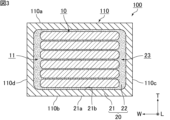
- FIG. 1 is a perspective view schematically showing an example of an electronic component according to an embodiment of the invention.
- FIG. 2 is a cross-sectional view of the electronic component shown in FIG. 1 along line XX.
- FIG. 3 is a cross-sectional view of the electronic component shown in FIG. 1 along line YY.
- FIG. 4 is a cross-sectional view of the electronic component shown in FIG. 1 along line YY, showing a state in which cracks have occurred inside.
- FIG. 5 is a cross-sectional view schematically showing an example of an electronic component according to another embodiment of the invention, and corresponds to the cross-sectional view taken along line YY in FIG. FIG.
- FIG. 6 is a cross-sectional view schematically showing an example of an electronic component according to still another embodiment of the invention, corresponding to the cross-sectional view taken along line YY in FIG.
- FIG. 7 is a cross-sectional view schematically showing an example of an electronic component according to still another embodiment of the invention, and corresponds to the cross-sectional view taken along line YY in FIG.
- FIG. 8 is a cross-sectional view schematically showing an example of an electronic component according to still another embodiment of the invention, corresponding to the cross-sectional view taken along line XX in FIG. 9 is a cross-sectional view schematically showing an example of a solid electrolytic capacitor element included in the electronic component shown in FIG. 1.
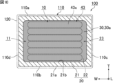
- FIG. 10 is a schematic front view of the first end surface of the electronic component element included in the electronic component shown in FIG.
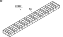
- FIG. 11 is a perspective view schematically showing an example of the first portion of the exterior body used in the method for manufacturing an electronic component according to the embodiment of the present invention, showing a state in which some through holes are seen through.
- 12 is a plan view of the first portion of the exterior body shown in FIG. 11.
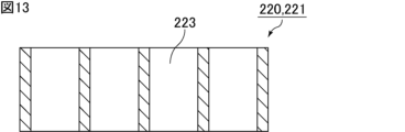
- FIG. 13 is a cross-sectional view of the first portion of the armor shown in FIG. 12, taken along line ZZ.
- FIG. 14 is a plan view schematically showing an example of a work used in the electronic component manufacturing method according to the embodiment of the present invention.
- FIG. 11 is a perspective view schematically showing an example of the first portion of the exterior body used in the method for manufacturing an electronic component according to the embodiment of the present invention, showing a state in which some through holes are seen through.
- 12 is a plan view of the first portion of the exterior body shown in FIG. 11.
- FIG. 13 is a cross-
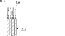
- FIG. 15 is a diagram schematically showing an example of a process of preparing a laminate in which a plurality of solid electrolytic capacitor elements are laminated.
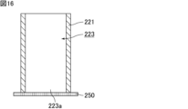
- FIG. 16 is a diagram schematically showing an example of a process of attaching an adhesive sheet to the first portion of the exterior body.
- FIG. 17 is a diagram schematically showing an example of the process of supplying the conductive paste onto the adhesive sheet.
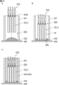
- FIG. 18A is a diagram schematically showing an example of a process of inserting a laminate into a through-hole;
- FIG. 18B is a diagram schematically showing an example of the process of embedding the first portion on the tip side of each element in the conductive paste.
- FIG. 18C is a diagram schematically showing an example of a process of filling a gap between each element (laminate) inserted into the through-hole and the first portion of the exterior body with a liquid material.
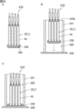
- FIG. 19A is a diagram schematically showing another example of the step of inserting the laminate into the through-hole.
- FIG. 19B is a diagram schematically showing another example of the step of embedding the first portion on the tip side of each element in the conductive paste.
- FIG. 19C is a diagram schematically showing another example of the process of filling the gap between each element (laminate) inserted into the through-hole and the first portion of the exterior body with a liquid material.
- FIG. 19A is a diagram schematically showing another example of the step of inserting the laminate into the through-hole.
- FIG. 19B is a diagram schematically showing another example of the step of embedding the first portion on the tip side of each element in the conductive paste.
- FIG. 19C is a diagram schematically showing another example of
- FIG. 20A is a diagram schematically showing an example of a process of applying a conductive paste to a laminate in which a plurality of solid electrolytic capacitor elements are laminated;
- FIG. 20B is a diagram schematically showing an example of a process of inserting each element (laminate) coated with a conductive paste into a through-hole.
- FIG. 20C is a diagram schematically showing an example of a process of arranging the conductive paste applied to the first portion on the tip side of each element on the adhesive sheet.
- FIG. 21 is a diagram schematically showing an example of a process of cutting the first portion of the exterior body around the through hole.
- the present invention is not limited to the following configurations, and can be appropriately modified and applied without changing the gist of the present invention. Combinations of two or more of the individual desirable configurations described below are also part of the present invention.
- FIG. 1 is a perspective view schematically showing an example of an electronic component according to an embodiment of the invention.
- FIG. 2 is a cross-sectional view of the electronic component shown in FIG. 1 along line XX.
- FIG. 3 is a cross-sectional view of the electronic component shown in FIG. 1 along line YY. Note that the illustration of the internal structure of the solid electrolytic capacitor element is omitted in FIG. 3 and FIGS. 4 to 7 described later.
- L indicates the length direction of the electronic component 100 and the electronic component base body 110
- W indicates the width direction
- T indicates the height direction.
- the length direction L, the width direction W, and the height direction T are orthogonal to each other.
- the electronic component 100 is a solid electrolytic capacitor, and has a substantially rectangular parallelepiped shape as shown in FIGS.
- Electronic component 100 includes electronic component base body 110 , first external electrodes 120 , and second external electrodes 130 .
- the electronic component base body 110 includes a solid electrolytic capacitor element 10 (hereinafter sometimes simply referred to as “element 10”) as an element (electronic component element), and a laminate (a plurality of It comprises a stack 11 in which the elements 10 are superimposed. Further, the electronic component base body 110 includes an exterior body 20 and current collecting electrodes 30 .
- the number of elements 10 included in the laminate 11 is not particularly limited as long as it is two or more, and can be set as appropriate.
- the electronic component base body 110 has a substantially rectangular parallelepiped outer shape.
- the electronic component base body 110 has a first main surface 110a and a second main surface 110b that face each other in the height direction T, a first side face 110c and a second side face 110d that face each other in the width direction W, and a length direction L that faces each other. It has a first end surface 110e and a second end surface 110f.
- the first end face 110e of the electronic component base body 110 is an example of the first face of the electronic component base body in the electronic component of the present invention
- the second end face 110f of the electronic component base body 110 is an example of the electronic component base body of the present invention. It is an example of the 2nd surface of the electronic component base in components.
- the electronic component base body 110 has a substantially rectangular parallelepiped outer shape, but the corners and ridges may be rounded.
- a corner is a portion where three surfaces of the electronic component base 110 intersect, and a ridge is a portion where two surfaces of the electronic component base 110 intersect.
- the exterior body 20 seals the multiple elements 10 . That is, the laminated body 11 of the plurality of elements 10 is embedded in the exterior body 20 . In addition, the exterior body 20 seals the collector electrode 30 . And the exterior body 20 has the 1st part 21 containing a 1st resin material, and the 2nd part 22 containing a 2nd resin material.
- the first portion 21 has a tubular structure with a through hole 23 and accommodates a plurality of elements 10 (laminate 11) in the through hole 23 .
- the second portion 22 exists within the through hole 23 in which the plurality of elements 10 (laminated body 11) are accommodated.
- FIG. 4 is a cross-sectional view of the electronic component shown in FIG. 1 along line YY, showing a state in which cracks have occurred inside.
- first portion 21 By forming the first portion 21 into a tube structure, as shown in FIG. Delamination at the interface absorbs the stress, and the propagation of the crack CR to the first portion 21 can be stopped.
- the second portion 22 existing in the through hole 23 is surrounded by the first portion 21 . That is, the joint interface between the first portion 21 and the second portion 22 is not exposed to the outer surface of the exterior body 20 . Therefore, it is possible to prevent the crack CR from being exposed from the joint interface to the outer surface.
- a sealing method that is, a method for forming the exterior body 20
- a method different from a conventional sealing method for example, transfer molding or press molding
- a resin material different from the sealing method of 1 can be selected, and a resin material having higher strength at high temperatures can be used for the exterior body 20 , especially the first portion 21 . Therefore, the strength of the exterior body 20 can be increased, and cracks are less likely to occur.
- the exterior body 20 includes the first portion 21 and the second portion 22. Since a resin material having high strength can be used as the first resin material of the first portion 21, the exterior body 20 can be The thickness can be made equal to or thinner than that of a conventional armor made of only one type of material.
- the first portion 21 of the tubular structure having the through hole 23 is open at both ends in the direction in which the through hole 23 extends (that is, the longitudinal direction or the axial direction of the pipe). , a plurality of elements 10 (laminated body 11) and a second portion 22 are accommodated.
- the first portion 21 constitutes the outermost periphery of the exterior body 20, and the surface of the first portion 21 includes an outer peripheral surface 21a, an inner peripheral surface 21b, and an end surface 21c on the first external electrode 120 side. and an end face 21d on the second external electrode 130 side.
- the first portion 21 is integrally molded into a tubular structure from a predetermined material including the first resin material, and the first portion 21 has no seams or internal joint interfaces.
- the second portion 22 is filled in the through holes 23 in which the plurality of elements 10 (laminated body 11) are accommodated. That is, the second portion 22 is filled inside the first portion 21 and around the plurality of elements 10 (laminated body 11).
- the state in which the second portions 22 are filled in the through holes 23 in which the plurality of elements 10 (laminated bodies 11) are accommodated means that the second portions 22 are inside the first portions 21 and The space around the plurality of elements 10 (laminated body 11) may or may not be completely filled. In the latter case, for example, a small amount of air bubbles may remain in the second portion 22, a slight gap may remain between the second portion 22 and the first portion 221, or the second portion 22 may A slight gap may remain between the and at least one element 10 .
- the shape of the cross section of the first portion 21 perpendicular to the direction in which the through hole 23 extends is not particularly limited, but the first portion 21, as shown in FIG. is preferably a substantially square tubular structure.
- the cross section of the first portion 21 perpendicular to the extending direction of the through hole 23 may be simply referred to as the "cross section".
- the “square tube structure” is a structure in which the outer peripheral surface of the tube structure includes four planes, and two adjacent planes among the four planes intersect each other (preferably orthogonally). , and the shape of the through hole 23 is not particularly limited.
- the outer peripheral surface 21a of the first portion 21 may be, for example, rectangular in cross section as shown in FIG. 3, and each corner of the rectangular outer peripheral surface 21a is rounded (R). You can In addition, the outer peripheral surface 21a of the first portion 21 may have an elliptical shape, a circular shape, or a trapezoidal shape (each corner may be rounded) in cross section.
- FIG. 5 is a cross-sectional view schematically showing an example of an electronic component according to another embodiment of the invention, corresponding to the cross-sectional view taken along line YY in FIG.
- FIG. 6 is a cross-sectional view schematically showing an example of an electronic component according to still another embodiment of the invention, corresponding to the cross-sectional view taken along line YY in FIG.
- the through hole 23 (the inner peripheral surface 21b of the first portion 21) has a round cross section (a cross section perpendicular to the extending direction of the through hole 23). It is preferably an attached polygon or a closed curve.
- stress concentration on the corners of the inner peripheral surface 21b of the first portion 21 when the internal pressure rises can be alleviated, so that the breakage of the first portion 21 and the exposure of cracks to the outside can be prevented. It is possible to suppress it and further improve the reliability.
- the through-hole 23 (the inner peripheral surface 21b of the first portion 21) may have a cross-sectional shape of a rectangle with rounded corners (see FIG. 3). It may be rectangular (see FIG. 5), elliptical (see FIG. 6), circular, or trapezoidal with rounded corners.
- FIG. 7 is a cross-sectional view schematically showing an example of an electronic component according to still another embodiment of the present invention, corresponding to the cross-sectional view taken along line YY in FIG.
- the cross-sectional shape of the through hole 23 may be a polygon with chamfered (cut off) corners. That is, as shown in FIG. 7, the through hole 23 (the inner peripheral surface 21b of the first portion 21) may have a polygonal cross-sectional shape with obtuse angles formed by each corner. Also in this case, it is possible to alleviate the stress concentration on the corners of the inner peripheral surface 21b of the first portion 21 when the internal pressure rises.
- the through-hole 23 (the inner peripheral surface 21b of the first portion 21) has a cross-sectional shape of a rectangle with chamfered corners, that is, a It may be octagonal with an obtuse angle.
- the through-hole 23 (the inner peripheral surface 21b of the first portion 21) may have a cross-sectional shape that is not rounded. , and trapezoids.
- FIG. 8 is a cross-sectional view schematically showing an example of an electronic component according to still another embodiment of the present invention, corresponding to the cross-sectional view taken along line XX in FIG.
- the first portion 21 has a tapered shape in which the cross-sectional area gradually changes (for example, gradually decreases) in the direction in which the through hole 23 extends (the same direction as the length direction L of the electronic component base body 110). may have a peripheral surface 1e of As a result, it is possible to reduce the positional variation of each element 10 in the manufacturing stage of the electronic component 100 and improve the positional accuracy.
- the through hole 23 is formed in the shape of a truncated quadrangular pyramid, the upper base of the truncated quadrangular pyramid is located on the first end surface 110 e of the electronic component body 110 , and the lower base of the truncated quadrangular pyramid is located on the electronic component body 110 . may be arranged so as to be positioned at the second end surface 110f of the .
- tapered peripheral surface 1e may be provided entirely from the end surface 21c of the first portion 21 on the first external electrode 120 side to the end surface 21d on the second external electrode 130 side, as shown in FIG. Alternatively, it may be provided only partly between the end face 21c and the end face 21d, for example, only on the end face 21c side.
- the first resin material may be the same material as the second resin material, but is preferably different from the second resin material. Using different materials makes it easier for separation to occur at the bonding interface between the second portion 22 and the first portion 21, so that propagation of cracks generated from the periphery of the element 10 can be more effectively stopped. is. In addition, since options for the first resin material are increased, a resin material having high strength at high temperatures can be easily selected as the first resin material.
- first resin material is the same material as the second resin material, it is possible to form a bonding interface between the second portion 22 and the first portion 21, and the bonding interface can be It is possible to cause delamination.
- the first resin material is preferably at least one thermoplastic resin
- the second resin material is preferably at least one thermosetting resin.
- the exterior body is usually made of thermosetting resin, but by using a thermoplastic resin as the first resin material, a material having higher strength at 150° C. or higher is used as the first portion 21 . 1 resin material. Further, by using a thermoplastic resin as the first resin material and a thermosetting resin as the second resin material, it is possible to easily manufacture the electronic component 100 having the first portion 21 of the tubular structure, as will be described later. .
- the melting point of at least one thermoplastic resin as the first resin material is preferably 260°C or higher, more preferably 275°C or higher, and even more preferably 300°C or higher.
- the melting point of a thermoplastic resin means a value measured according to differential scanning calorimetry (DSC) in JIS K7121.
- the upper limit of the melting point of at least one thermoplastic resin is not limited, it is usually 400°C or lower, preferably 360°C or lower, and more preferably 330°C or lower.
- the first resin material contains, as at least one thermoplastic resin, at least one resin selected from the group consisting of PPS (polyphenylene sulfide), LCP (liquid crystal polymer), PBT (polybutylene terephthalate), polyimide and polyamide. preferably included.
- PPS polyphenylene sulfide
- LCP liquid crystal polymer
- PBT polybutylene terephthalate
- polyimide polyimide
- polyamide polyamide
- These resins have high strength at 150° C. or higher, and are materials that can be processed into a tubular shape, which is the shape of the first portion 21, by injection molding, which is generally used as a molding method for thermoplastic resins. It is suitable as a resin material.
- the second resin material preferably contains at least one resin selected from the group consisting of epoxy resin, silicon resin and urethane resin as at least one thermosetting resin.
- materials that are liquid at room temperature before curing are suitable because they are handled at room temperature, and these resins may correspond to such materials.
- these resins are also suitable as capacitor sealing materials in terms of insulation, heat resistance, and the like.
- the first resin material and the second resin material may each contain fillers such as silica particles, alumina particles, and metal particles, and fibers such as ceramic fibers, as reinforcing materials.
- the first resin material preferably contains ceramic fibers having a fiber length of 50 ⁇ m or more as a reinforcing material.
- a plurality of elements 10 are stacked in the height direction T.
- the extending direction of each of the plurality of elements 10 is substantially parallel to the first main surface 110 a and the second main surface 110 b of the electronic component base body 110 .
- Elements 10 adjacent to each other in the height direction T may be bonded together via a conductive adhesive (not shown).
- FIG. 9 is a cross-sectional view schematically showing an example of a solid electrolytic capacitor element included in the electronic component shown in FIG.
- each solid electrolytic capacitor element 10 is a substantially flat plate-like electronic component element, and has a rectangular thin film (foil) when viewed from above and is composed of a valve-acting metal substrate having a porous surface. ), a dielectric layer 41 (see FIG. 9, not shown in FIG. 2) provided on the surface of the anode 40 except for the base end surface 40b of the anode 40, and the base end surface 40b of the anode 40 and a mask layer 42, which is a linear (extending in a strip) insulating member, provided on the dielectric layer 41 along the dielectric layer 41. and a cathode 43 formed by In each solid electrolytic capacitor element 10 , cathode 43 faces anode 40 with dielectric layer 41 interposed therebetween.
- each cathode 43 corresponds to the first internal electrode of the electronic component of the invention
- each anode 40 corresponds to the second internal electrode of the electronic component of the invention. That is, each solid electrolytic capacitor element 10 has an anode 40 as a second internal electrode and a cathode 43 as a first internal electrode. includes a plurality of cathodes 43 as first internal electrodes and a plurality of anodes 40 as a plurality of second internal electrodes.
- the anode 40 extends between the first end surface 110e and the second end surface 110f of the electronic component base body 110, and extends between the first portion 40c on the side of the first end surface 110e and the second portion 40d on the side of the second end surface 110f.
- the first portion 40c on the side of the first end surface 110e is an example of the first portion on the side of the first surface of the second internal electrode in the electronic component of the present invention
- the second portion 40d on the side of the second end surface 110f is 4A and 4B are an example of a second portion on the second surface side of the second internal electrode in the electronic component of the present invention.
- the cathode 43 extends between the first end surface 110e and the second end surface 110f of the electronic component base body 110, and extends between the first portion 43a on the first end surface 110e side and the second portion 43b on the second end surface 110f side.
- the first portion 43a on the side of the first end surface 110e is an example of the first portion on the side of the first surface of the first internal electrode in the electronic component of the present invention
- the second portion 43b on the side of the second end surface 110f is 4A and 4B are an example of a second portion on the second surface side of the first internal electrode in the electronic component of the present invention.
- the cathode 43 has an end surface 43c on the side of the first external electrode 120 substantially parallel to the first end surface 110e of the electronic component element 110, and the first principal surface 110a and the second principal surface 110b of the electronic component element 110. It has a pair of parallel main surfaces and a pair of side surfaces substantially parallel to the first side surface 110c and the second side surface 110d of the electronic component base body 110. , a portion of each main surface of the cathode 43 on the side of the first external electrode 120 and a portion of each side surface of the cathode 43 on the side of the first external electrode 120 .
- the cathode 43 includes a solid electrolyte layer 44 provided on the dielectric layer 41, a carbon layer 45 provided on the solid electrolyte layer 44, and a cathode conductor layer 46 provided on the carbon layer 45. have.
- first portion of the cathode means a portion from the tip of the cathode on the side of the first external electrode to a point a predetermined distance away
- second portion of the cathode refers to the second portion of the cathode. It means a portion from the tip of the external electrode to a point separated by a predetermined distance, and both of them may be the ends of the cathode. More specifically, when the total length of the cathode 43 in the length direction L is Lc, the first portion 43a extends from the tip of the cathode 43 on the side of the first external electrode 120 to a point separated by 0.05 ⁇ Lc. may represent the part of The same is true for the first and second portions of the anode.
- FIG. 10 is a schematic front view of the first end face of the electronic component element included in the electronic component shown in FIG.
- the collector electrode 30 is electrically connected to the plurality of cathodes 43 of the plurality of elements 10 . As shown in FIGS. 2 and 10, the collector electrode 30 is exposed on the first end face 110e of the electronic component element 110, and is provided at least on the first end face 110e side of the electronic component element 110. there is Moreover, the collector electrode 30 is formed in a shape having a thickness at a position recessed from the first end surface 110e (the end surface 21c of the first portion 21).
- the first portion 43a of each cathode 43 is embedded in the collecting electrode 30, thereby ensuring electrical connection between each cathode 43 and the collecting electrode 30. It is That is, the end face 30b of the collector electrode 30 on the side of the second external electrode 130 is positioned closer to the second external electrode 130 than the end face 43c of each cathode 43 on the side of the first external electrode 120 . Moreover, the current collecting electrode 30 is provided from the end surface 43c of each cathode 43 over each of the pair of main surfaces and the pair of side surfaces of each cathode 43, and is in contact with these surfaces.
- At least the first portion 43a of each cathode 43 is embedded in the current collecting electrode 30, and the position of the end surface 30b of the current collecting electrode 30 is particularly limited as long as it is within the range where the cathode 43 is provided. However, from the viewpoint of short circuit prevention, it is preferably within the range where the cathode conductor layer 46 is provided. Moreover, from the viewpoint of reducing the amount of material used for the collector electrode 30, the collector electrode 30 may be provided only in the vicinity of the first end surface 110e of the electronic component base body 110. FIG.
- the end surface 30b of the collector electrode 30 is 0.2 ⁇ Lc (preferably may not exceed a point separated by 0.1 x Lc, more preferably 0.05 x Lc).
- the collecting electrode 30 is arranged inside the first portion 21 of the tube structure. That is, the collector electrode 30 is arranged inside the through hole 23 . 2 and 10, the collector electrode 30 and the first portion 21 form the first end surface 110e of the electronic component element body 110. As shown in FIGS. That is, the end surface 30a of the current collecting electrode 30 on the side of the first external electrode 120 and the end surface 21c of the first portion 21 of the exterior body 20 on the side of the first external electrode 120 are flush with each other (on the same plane). positioned).
- each cathode 43 is not exposed to the first end surface 110e of the electronic component element body 110, but even if the end surface 43c of at least one cathode 43 is exposed to the first end surface 110e, good. That is, while the end surface 43 c of at least one cathode 43 is exposed from the current collecting electrode 30 , at least a region forming the first portion 43 a of each main surface and each side surface of the cathode 43 is in contact with the current collecting electrode 30 . You may have In this specification, even in such a case, "the first portion of the cathode (first internal electrode) is embedded in the collector electrode".
- the current collecting electrode 30 , the first portion 21 of the exterior body 20 and the at least one cathode 43 are located on the first end surface of the electronic component base body 110 .
- 110e is formed, and the end surface 30a of the current collecting electrode 30, the end surface 21c of the first portion 21 of the exterior body 20, and the end surface 43c of at least one cathode 43 are flush with each other (located on the same plane). .
- the second portion 22 of the package 20 is not exposed on the first end surface 110e of the electronic component base body 110, but the second portion 22 of the package 20 is exposed on the first end surface 110e. May be exposed.
- the current collecting electrode 30, the first portion 21 of the exterior body 20, and the second portion 22 of the exterior body 20 form the first end surface 110e of the electronic component base body 110, and the end surface 30a of the current collecting electrode 30,
- the end face 21c of the first portion 21 of the exterior body 20 and the end face of the second portion 22 of the exterior body 20 on the first external electrode 120 side are flush with each other (located on the same plane).
- the end surface 43c of at least one cathode 43 and the second portion 22 of the outer package 20 may be exposed to the first end surface 110e.
- the collector electrode 30, the first portion 21 of the package 20, at least one cathode 43, and the second portion 22 of the package 20 form the first end face 110e of the electronic component element 110
- the collector electrode 30, the end surface 21c of the first portion 21 of the exterior body 20, the end surface 43c of at least one cathode 43, and the end surface of the second portion 22 of the exterior body 20 on the side of the first external electrode 120 are planes. become one (located on the same plane).
- the collector electrode 30 is a composite material of a conductive component (conductive material) and a resin component (resin material).
- the conductive component preferably contains, as a main component, an elemental metal such as silver, copper, nickel, or tin, or an alloy containing at least one of these metals.
- the resin component preferably contains an epoxy resin, a phenol resin, or the like as a main component.
- the collector electrode 30 can be formed using, for example, a conductive paste such as silver paste.
- the first external electrode 120 is provided on the first end face 110e of the electronic component base body 110. As shown in FIG. In FIG. 1, the first external electrode 120 is provided from the first end surface 110e of the electronic component element body 110 over each of the first main surface 110a, the second main surface 110b, the first side surface 110c and the second side surface 110d. It is The first external electrode 120 is electrically connected to the collector electrode 30 exposed from the electronic component element body 110 at the first end surface 110e. That is, the first external electrode 120 is electrically connected to each cathode 43 via the collector electrode 30 .
- each element 10 and the collector electrode 30, which is a collector are in three-dimensional contact rather than two-dimensional contact.
- the electrical connection between each element 10 and the collector electrode 30 is stabilized (reduction in equivalent series resistance).
- the mechanical strength of these contacts is also improved.
- the stability and mechanical strength of electrical connection between the cathodes 43 and the first external electrodes 120 electrically connected to the cathodes 43 via the collector electrodes 30 are improved.
- the collector electrodes 30 are present in the through holes 23 in which the plurality of elements 10 (laminated body 11 ) are accommodated, and the collector electrodes 30 and the first portion 21 of the exterior body 20 are connected to the electronic component base body 110 .
- the first external electrode 120 can be formed on the first end face 110e. Therefore, electrical connection between the first external electrode 120 and the collector electrode 30 is easy, and the first external electrode 120 can be formed with a small thickness.
- the first external electrode 120 may have a so-called sputtered film formed by a sputtering method.
- materials for the sputtered film include Ni, Sn, Ag, Cu, and Ag.
- the first external electrode 120 may have a so-called deposited film formed by a deposition method.
- the material of the deposited film include Ni, Sn, Ag, Cu, and the like.
- the film thickness of the first external electrode 120 can be smaller than the film thickness of the second external electrode 130. good.
- the film thickness of the first external electrode 120 is preferably 1 ⁇ m or more and 100 ⁇ m or less, more preferably 5 ⁇ m or more and 50 ⁇ m or less, and even more preferably 10 ⁇ m or more and 30 ⁇ m or less.
- the second external electrode 130 is provided on the second end face 110f of the electronic component element 110.
- the second external electrode 130 is provided from the second end surface 110f of the electronic component element body 110 over each of the first main surface 110a, the second main surface 110b, the first side surface 110c and the second side surface 110d. It is The second external electrode 130 is electrically connected to the second portion 40d of the anode 40 (valve metal substrate) of the element 10 exposed from the electronic component base 110 at the second end surface 110f.
- Second external electrode 130 may be directly or indirectly connected to anode 40 (second portion 40d) at second end surface 110f of electronic component base 110 .
- At least one of the first external electrode 120 and the second external electrode 130 may have a resin electrode layer containing a conductive component and a resin component.
- the conductive component preferably contains, as a main component, an elemental metal such as silver, copper, nickel, or tin, or an alloy containing at least one of these metals.
- the resin component preferably contains an epoxy resin, a phenol resin, or the like as a main component.
- the resin electrode layer can be formed using, for example, a conductive paste such as silver paste.
- At least one of the first external electrode 120 and the second external electrode 130 may have a so-called plated layer formed by a plating method.
- plating layers include zinc/silver/nickel layers, silver/nickel layers, nickel layers, zinc/nickel/gold layers, nickel/gold layers, zinc/nickel/copper layers, and nickel/copper layers.
- a copper plated layer, a nickel plated layer, and a tin plated layer are preferably provided in this order (or with the exception of some plated layers).
- At least one of the first external electrode 120 and the second external electrode 130 may have both a resin electrode layer and a plating layer.
- the first external electrode 120 may have a resin electrode layer connected to the collector electrode 30 and an outer plated layer provided on the surface of the resin electrode layer.
- the first external electrode 120 includes an inner plated layer connected to the collector electrode 30, a resin electrode layer provided to cover the inner plated layer, and an outer plated layer provided on the surface of the resin electrode layer.
- the second external electrode 130 may have a resin electrode layer connected to the anode 40 (valve metal substrate) and an outer plated layer provided on the surface of the resin electrode layer.
- the second external electrode 130 includes an inner plated layer connected to the anode 40 (valve action metal substrate), a resin electrode layer provided to cover the inner plated layer, and a resin electrode layer provided on the surface of the resin electrode layer. and an outer plated layer.
- Electronic component 100 can be manufactured by the following method. In the following example, a method for simultaneously manufacturing a plurality of solid electrolytic capacitor elements using a large-sized valve action metal substrate will be described.
- FIG. 11 is a perspective view schematically showing an example of the first portion of the exterior body used in the method of manufacturing an electronic component according to the embodiment of the present invention, showing a state in which a part of the through holes are seen through.
- 12 is a plan view of the first portion of the exterior body shown in FIG. 11.
- FIG. 13 is a cross-sectional view of the first portion of the armor shown in FIG. 12, taken along line ZZ.
- a first portion 221 (a member to be the first portion 21 of the exterior body 20) of the exterior body 220 containing the above-described first resin material and having a plurality of through holes 223 is prepared.
- the first portion 221 is a member in which a plurality of through holes 223 are provided vertically and horizontally in a flat plate material having a predetermined thickness and a rectangular shape in a plan view. Each through hole 223 is provided in a direction perpendicular to the main surface of the first portion 221, and both ends thereof are open.
- the first portion 221 can be made by injection molding.
- each corner inside each through hole 223 of the first portion 221 may be rounded (see FIGS. 3, 5 and 6) or cornered (formed with an inclined surface, see FIG. 7). .
- the laminated body 11 is prepared.
- FIG. 14 is a plan view schematically showing an example of a work used in the electronic component manufacturing method according to the embodiment of the present invention.
- a workpiece 210 is prepared in which element parts 212 (a plurality of solid electrolytic capacitor elements 10) are connected to strip-shaped holding parts 211 at regular intervals.
- valve action metal substrate having a porous portion on its surface is cut by laser processing, punching, or the like to be processed into a shape including a plurality of element portions 212 and holding portions 211 .
- the valve action metal substrate is composed of, for example, a single metal such as aluminum, tantalum, niobium, titanium, or zirconium, or a valve action metal such as an alloy containing these metals.
- the valve action metal substrate may be composed of a core portion and a porous portion provided on at least one main surface of the core portion. A material obtained by forming a porous fine-powder sintered body or the like can be used as appropriate.
- mask layers are formed on both main surfaces and both side surfaces of the element portions 212 along the short sides of each element portion 212 .
- the mask layer is formed, for example, by applying a mask material such as a composition containing an insulating resin by screen printing, roller transfer, dispenser, inkjet printing, or the like.
- a mask material such as a composition containing an insulating resin
- insulating resins include polyphenylsulfone (PPS), polyethersulfone (PES), cyanate ester resin, fluorine resin (tetrafluoroethylene, tetrafluoroethylene-perfluoroalkyl vinyl ether copolymer, etc.), and soluble polyimide.
- Compositions comprising siloxane and epoxy resins, polyimide resins, polyamideimide resins, derivatives or precursors thereof, and the like are included.
- a hydrophilic member may or may not be applied to the mask layer.
- the valve-acting metal substrate is anodized to form an oxide film that will become a dielectric layer on the surface of the valve-acting metal substrate.
- the dielectric layer is composed of an oxide of aluminum.
- an oxide film is also formed on the side surfaces of the element portion 212 cut by laser processing, punching, or the like.
- a chemically processed foil on which aluminum oxide has already been formed may be used as the valve action metal substrate.
- an oxide film is formed on the side surface of the cut element part 212 by anodizing the valve metal substrate after cutting.
- a solid electrolyte layer is formed on the dielectric layer of the element section 212 .
- the porous portion of the valve action metal base is impregnated with the treatment liquid.
- the element part 212 is pulled out of the treatment liquid and dried at a predetermined temperature for a predetermined time.
- a solid electrolyte layer is formed by repeating immersion in the treatment liquid, pulling up, and drying a predetermined number of times.
- a treatment liquid containing a solid electrolyte for example, a dispersion of conductive polymers such as polypyrroles, polythiophenes, and polyanilines is used. Among these, polythiophenes are preferred, and poly(3,4-ethylenedioxythiophene) called PEDOT is particularly preferred.
- the conductive polymer may contain a dopant such as polystyrene sulfonic acid (PSS).
- PSS polystyrene sulfonic acid
- a conductive polymer film can be formed by applying a conductive polymer dispersion to the outer surface of the dielectric layer and drying it.
- a liquid containing a polymerizable monomer such as 3,4-ethylenedioxythiophene and an oxidizing agent may be used as the treatment liquid containing the solid electrolyte.
- the liquid contained can be adhered to the outer surface of the dielectric layer to form a conductive polymer film by chemical polymerization. This conductive polymer film becomes the solid electrolyte layer.
- a carbon paste is a conductive paste containing carbon particles as a conductive component and a resin component such as an epoxy resin or a phenol resin.
- the cathode conductor layer is formed in a predetermined region by immersing the element portion 212 in the conductive paste, pulling it out, and drying it.
- the conductive paste for forming the cathode conductor layer include those containing metal particles as a conductive component and resin components such as epoxy resin and phenol resin.
- metal particles include gold, silver, copper, and platinum.
- a silver paste containing silver particles as a conductive component is suitable as the conductive paste for forming the cathode conductor layer.
- substantially rectangular parallelepiped through-holes 223 are formed at the same number and pitch as the elements 10 of the strip-shaped workpiece 210, and a plurality of rows of such through-holes 223 are provided.
- FIG. 15 is a diagram schematically showing an example of a process of preparing a laminate in which a plurality of solid electrolytic capacitor elements are laminated.
- a plurality of strip-shaped workpieces 210 having a plurality of elements 10 formed thereon are prepared, and a predetermined number of workpieces 210 are bundled and clamped so that the plurality of elements 10 are stacked. or the like (not shown).
- a plurality of elements 10 are laminated to form a plurality of laminates 11 each including a plurality of cathodes and a plurality of anodes. Note that the plurality of laminates 11 are arranged in a line (a line aligned in a direction perpendicular to the plane of FIG. 15).
- FIG. 16 is a diagram schematically showing an example of the process of attaching the adhesive sheet to the first portion of the exterior body.
- an adhesive sheet 250 (hereinafter sometimes simply referred to as "sheet 250") is attached to the first portion 221 so as to close the first opening 223a of each through hole 223. paste. That is, the adhesive sheet 250 is attached to the entire surface of the first portion 221 to close one side of each through-hole 223 .
- each through-hole 223 may be in a state where the first opening 223a (lower opening) is covered.
- the first opening 223a may be capped by placing a lid on it.
- FIG. 17 is a diagram schematically showing an example of the process of supplying the conductive paste onto the adhesive sheet.
- the sheet is removed from the second opening 223b (upper opening) of each through-hole 223.
- a conductive paste 230 is applied over 250 .
- the conductive paste 230 is applied on the sheet 250 inside each through-hole 223 .
- the conductive paste 230 include those containing metal particles as a conductive component and resin components such as epoxy resin and phenol resin.
- metal particles include silver, copper, nickel, and tin.
- a silver paste containing silver particles as a conductive component is suitable.
- a dispenser or the like can be used to supply the conductive paste 230 .
- FIG. 18A is a diagram schematically showing an example of the process of inserting the laminate into the through-hole.
- FIG. 18B is a diagram schematically showing an example of the process of embedding the first portion on the tip side of each element in the conductive paste.
- FIG. 18C is a diagram schematically showing an example of a process of filling a gap between each element (laminate) inserted into the through-hole and the first portion of the exterior body with a liquid material.
- the plurality of fixed works 210 are moved relatively to the first portion 221, and the stacked body 11 (cathode) is inserted into the through holes 223 in the same row from the second opening 223b. and anode).
- the elements 10 (cathode and anode) can be inserted into the first portion 221 in strip units. Therefore, the productivity can be greatly improved compared to inserting the elements 10 one by one or the laminated bodies 11 one by one into the first portion 221 .
- the conductive paste 230 is spread by the tip of each element 10, that is, the first portion 43a of the cathode 43, and at least the first portion 43a on the tip side of the cathode 43 of each element 10 is spread. are embedded in the conductive paste 230 . That is, all the elements 10 are connected with the conductive paste 230 .
- the conductive paste 230 is cured on the sheet 250 by, for example, heating.
- the collector electrode 30 is formed in a state in which at least the first portion 43a on the tip side of the cathode 43 of each element 10 is embedded in the collector electrode 30 (see FIG. 2).
- each element 10 and the current collecting electrode 30 as a current collecting portion are in three-dimensional contact instead of two-dimensional contact, and the current between each element 10 and the current collecting electrode 30 is reduced. stable connection (decrease in equivalent series resistance).
- the mechanical strength of these contacts is also improved. As a result, the stability and mechanical strength of electrical connection between the cathodes 43 and the first external electrodes 120 electrically connected to the cathodes 43 via the collector electrodes 30 are improved.
- the liquid material 222 is filled in the gap between each element 10 (cathode and anode) inserted into each through-hole 223, that is, the laminate 11 and the first portion 221.
- the liquid material is injected into the gap between the first portion 221 and each element 10 (cathode and anode), that is, the laminate 11 . 222.
- the viscosity of the liquid material 222 may be reduced by heating during injection or vacuum defoaming.
- the liquid material 222 contains the above-described second resin material (however, it is in liquid form before hardening).
- the resin contained in the second liquid resin material is preferably a thermosetting resin such as an epoxy resin, a silicone resin, or a urethane resin.
- the liquid material 222 before curing preferably has a viscosity of 100 Pa ⁇ s or less at 25°C. If the viscosity is 100 Pa ⁇ s or less, the product can be easily filled simply by defoaming and heating in a vacuum oven, thereby improving productivity.
- the viscosity of the liquid material 222 before curing is preferably 30 Pa ⁇ s or less at 25° C., more preferably 5 Pa ⁇ s or less.
- the viscosity of the liquid material 222 before hardening referred to here is the viscosity measured at 25° C. by the double cylinder method.
- the viscosity of the liquid material 222 before curing is usually 0.01 Pa ⁇ s or more, preferably 0.1 Pa ⁇ s or more, and more preferably 0.3 Pa ⁇ s at 25°C. That's it.
- the liquid material 222 filled in the gap between each element 10 (laminate 11) and the first portion 221 is cured.
- the liquid material 222 is heated and hardened in a vacuum oven to form the second portion 222a of the exterior body 220 (the portion that becomes the second portion 22 of the exterior body 20).
- a few air bubbles may remain in the second portion 222a, which is the cured product of the liquid material 222.
- a slight gap may remain between the second portion 222 a and the first portion 221 and/or between the second portion 222 a and the at least one element 10 .
- the conductive paste 230 is supplied, the plurality of elements 10 (laminated bodies 11) are inserted, the liquid material 222 is filled, and the liquid material 222 is cured.
- a plurality of elements 10 (laminated bodies 11) and second portions 222a are housed in all the through holes 223.
- FIG. 19A is a diagram schematically showing another example of the process of inserting the laminate into the through-hole.
- FIG. 19B is a diagram schematically showing another example of the step of embedding the first portion on the tip side of each element in the conductive paste.
- FIG. 19C is a diagram schematically showing another example of the process of filling the gap between each element (laminate) inserted into the through-hole and the first portion of the exterior body with a liquid material.
- the through-hole 223 may have a tapered peripheral surface 221e with a smaller cross-sectional area in the direction in which the multiple elements 10 (laminated body 11) are inserted.
- the plurality of elements 10 laminated body 11
- the positions of the plurality of elements 10 are corrected along the tapered peripheral surface 221e, and their positions can be adjusted. Therefore, as shown in FIG. 19C, the gap between each element 10 (laminate 11) and the first portion 221 is filled with the liquid material 222 while the positions of the plurality of elements 10 are properly controlled. can be done.
- FIG. 20A is a diagram schematically showing an example of a process of applying a conductive paste to a laminate in which a plurality of solid electrolytic capacitor elements are laminated.
- FIG. 20B is a diagram schematically showing an example of a process of inserting each element (laminate) coated with a conductive paste into a through-hole.
- FIG. 20C is a diagram schematically showing an example of a process of arranging the conductive paste applied to the first portion on the tip side of each element on the adhesive sheet.
- a jig such as a clamp
- the conductive paste 230 may be applied to the first portion 43 a on the side, for example, at least the tip portion of each element 10 . This allows the conductive paste 230 to be connected to all the elements 10 .
- each through hole 223 covered with, for example, an adhesive sheet 250
- each A plurality of elements 10 (cathode and anode) with conductive paste 230 applied to cathode 43, that is, laminate 11 is inserted, and conductive paste 230 and elements 10 (laminate 11) may be arranged.
- the conductive paste 230 may be cured on the sheet 250 by heating or the like while the elements 10 (cathode and anode), that is, the laminate 11 are inserted into the through holes 223 .
- At least the first portion 43a of the cathode 43 of each element 10 is embedded in the collector electrode 30 also by these steps.
- the liquid material 222 is poured into the gap between each element 10 (cathode and anode) inserted into each through-hole 223, that is, the laminate 11 and the first portion 221.
- the filled liquid material 222 may be cured.
- the sheet 250 is peeled off from the first portion 221 .
- the collector electrode 30 to which each element 10 is connected is exposed on the peeled surface, and this peeled surface becomes the first end face 110 e of the electronic component element 110 . At least one cathode end face may be exposed to the release surface.
- the unnecessary portion of the elements 10 there are unnecessary portions of the elements 10, unnecessary portions of the liquid material 222, and a holding portion 211 for the workpiece 210.
- the height of the first portion 221 is the length in the longitudinal direction of the chip, it is necessary to adjust the height to a predetermined length. Therefore, the unnecessary portion of the upper portion of the first portion 221 is scraped off with a grinder or the like. The surface exposed by scraping away unnecessary portions becomes the second end surface 110 f of the electronic component base body 110 .
- the anode 40 of each element 10 (a foil made of a valve action metal substrate) is exposed to the second end face 110f.
- FIG. 21 is a diagram schematically showing an example of a process of cutting the first portion of the exterior body around the through-hole.
- the first portion 221 is cut around each through-hole 223 .
- the first portion 21 of the tubular structure can be easily formed from the first portion 221 .
- a predetermined cut line (chain line in FIG. 21) outside each through-hole 223 is cut with a dicer or the like.
- an electronic component base body 110 including the laminate 11 of the element 10 is obtained.
- the electronic component base body 110 may be barrel-polished. Specifically, the electronic component element 110 may be polished by enclosing the electronic element element 110 together with an abrasive in a barrel and rotating the barrel element. As a result, the corners and ridges of the electronic component base 110 are rounded.
- fine metal particles may be ejected and collided with the second end face 110f (anode end face) of the barrel-polished electronic component element body 110 by an aerosol deposition method, if necessary. Thereby, a metal film may be formed on each base end surface 40b of the anode 40 exposed at the second end surface 110f (anode end surface) of the electronic component element body 110 .
- a first external electrode 120 and a second external electrode 130 are formed on the first end surface 110e (cathode end surface) and the second end surface 110f (anode end surface) of the electronic component element body 110, respectively.
- a conductive paste is applied by screen printing or the like and cured to form resin electrode layers as the first external electrode 120 and the second external electrode 130, respectively.
- the conductive paste for forming the resin electrode layer a silver paste containing silver particles as a conductive component is suitable. After that, a plated layer may be formed on the resin electrode layer by plating.
- the collector electrode 30 is arranged inside the first portion 21 , and the collector electrode 30 and the first portion 21 of the exterior body 20 form the first end surface 110 e of the electronic component element body 110 .
- the first external electrode 120 is formed on the first end face 110e. Therefore, since electrical connection between the first external electrode 120 and the collector electrode 30 is easy, the first external electrode 120 can be formed with a small thickness.
- a thin first external electrode 120 (sputtered film and/or vapor-deposited film) having a thickness of, for example, several ⁇ m may be formed by a sputtering method or a vapor deposition method. As a result, it becomes easier to control and uniformize the outer size of the chip, and a reduction in the amount of materials used can be expected.
- the electronic component 100 (solid electrolytic capacitor) can be obtained by the above method.
- the exterior body 20 is composed of only two types of resin materials, that is, the first part 21 and the second part 22. It may be made of a resin material.
- one or more intermediate resin layers made of a resin material may be provided between the first portion and the second portion.
- Such an intermediate resin layer is formed, for example, by forming the second portion for sealing the laminate of a plurality of solid electrolytic capacitor elements with a size smaller than that of the through hole of the first portion by transfer molding or the like. It is formed by inserting the laminate of electrolytic capacitor elements together with the second portion into the through hole of the first portion, filling the gap between the second portion and the first portion with a liquid resin material, and curing the material. can do.
- the exterior body in the electronic component of the present invention may be composed of only one type of resin material.
- only the second portion 22 may be provided without providing the first portion 21 .
- Such an electronic component can be manufactured, for example, by setting a cut line inside each through-hole 223 and cutting and removing all the first portions 221 in a cutting process for singulation.
- the substantially rectangular parallelepiped electronic component base body 110 has been described.
- it may be, for example, a columnar shape in addition to a substantially rectangular parallelepiped shape.
- Electronic component bodies 110 may be produced one by one using the first portion having only one hole.
- the electronic component 100 is a solid electrolytic capacitor
- the electronic component of the present invention is not particularly limited as long as it includes an element (electronic component element) and an exterior body.
- solid electrolytic capacitors for example, film capacitors, electric double layer capacitors, solid batteries and the like may also be used.
Landscapes
- Engineering & Computer Science (AREA)
- Power Engineering (AREA)
- Microelectronics & Electronic Packaging (AREA)
- Manufacturing & Machinery (AREA)
- Chemical & Material Sciences (AREA)
- Chemical Kinetics & Catalysis (AREA)
- Electrochemistry (AREA)
- General Chemical & Material Sciences (AREA)
- Fixed Capacitors And Capacitor Manufacturing Machines (AREA)
Abstract
第1内部電極43と、第2内部電極40と、導電材料及び樹脂材料の複合材料である集電電極30と、上記第1内部電極43、上記第2内部電極40及び上記集電電極30を封止する外装体20とを含み、第1面110e及び第2面110fを有する電子部品素体110と、上記第1面110eに形成された第1外部電極120と、上記第2面110fに形成された第2外部電極130と、を備え、上記第1内部電極43と上記第2内部電極40とは、各々、上記第1面110eと上記第2面110fとの間に延設され、上記第1面110e側の第1部分43a、40cと、上記第2面110f側の第2部分43b、40dとを有し、上記第1内部電極43の上記第1部分43aは、上記集電電極30内に埋め込まれており、上記集電電極30は、上記第1面110eにおいて上記第1外部電極120と接続されており、上記第2内部電極40の上記第2部分40dは、上記第2面110fにおいて上記第2外部電極130と接続されている、電子部品100。
Description
本発明は、電子部品及び電子部品の製造方法に関する。
特許文献1には、樹脂でパッケージ外装したチップタイプの高分子アルミ電解コンデンサにおいて、積層したコンデンサ素子の陽極と陰極をチップ端面まで引き出し、その端面に導電性の膜を形成することで、複数の素子を集電し、外部電極とする構造が開示されている(図10参照)。
特許文献1に開示された上記構造においては、複数のコンデンサ素子の陰極の集電・引き出しを外装体の端面が存在する面と同じ面にて行うことになる。この場合、陰極の位置が揃っていない(面一になっていない)と、奥まっている素子は端面での集電ができなくなり電気的な接続が不安定となり(等価直列抵抗の増加)、反対に、出っ張っている素子があれば、製品サイズが大きくなる不具合が生じる。また、外装体の端面と集電部材である外部電極との間に構造的な界面ができるため、この界面で外部電極に剥がれが生じる等の構造面でのウィークポイントにもなる。
本発明は、上記の問題を解決するためになされたものであり、外部電極と内部電極との間における電気的な接続の安定性及び機械的な強度に優れた電子部品を提供することを目的とする。さらに、本発明は、外部電極と内部電極との間における電気的な接続の安定性及び機械的な強度に優れた電子部品を実現可能な電子部品の製造方法を提供することを目的とする。
本発明の電子部品は、第1内部電極と、第2内部電極と、導電材料及び樹脂材料の複合材料である集電電極と、上記第1内部電極、上記第2内部電極及び上記集電電極を封止する外装体とを含み、第1面及び第2面を有する電子部品素体と、上記第1面に形成された第1外部電極と、上記第2面に形成された第2外部電極と、を備え、上記第1内部電極と上記第2内部電極とは、各々、上記第1面と上記第2面との間に延設され、上記第1面側の第1部分と、上記第2面側の第2部分とを有し、上記第1内部電極の上記第1部分は、上記集電電極内に埋め込まれており、上記集電電極は、上記第1面において上記第1外部電極と接続されており、上記第2内部電極の上記第2部分は、上記第2面において上記第2外部電極と接続されている。
本発明の電子部品の製造方法は、第1樹脂材料を含み、貫通孔を有する外装体の第1部分を準備する工程と、第1内部電極及び第2内部電極を準備する工程と、上記貫通孔の第1の開口に蓋をした状態で、上記貫通孔の第2の開口から上記蓋上に導電性ペーストを供給する工程と、上記第2の開口から上記貫通孔内に上記第1内部電極及び上記第2内部電極を挿入し、上記第1内部電極の先端側の第1部分を上記導電性ペースト内に埋め込む工程と、上記第1内部電極が埋め込まれた状態で、上記蓋上で上記導電性ペーストを硬化させる工程と、を含む。
本発明の他の電子部品の製造方法は、第1樹脂材料を含み、貫通孔を有する外装体の第1部分を準備する工程と、第1内部電極及び第2内部電極を準備する工程と、上記第1内部電極の先端側の第1部分に導電性ペーストを塗布する工程と、上記貫通孔の第1の開口に蓋をした状態で、上記貫通孔の第2の開口から、上記導電性ペーストが塗布された上記第1内部電極を挿入し、上記蓋上に上記導電性ペーストを配置する工程と、上記第1内部電極が上記貫通孔内に挿入された状態で、上記蓋上で上記導電性ペーストを硬化させる工程と、を含む。
本発明によれば、外部電極と内部電極との間における電気的な接続の安定性及び機械的な強度に優れた電子部品を提供することができる。さらに、本発明によれば、外部電極と内部電極との間における電気的な接続の安定性及び機械的な強度に優れた電子部品を実現可能な電子部品の製造方法を提供することができる。
以下、本発明の電子部品及び電子部品の製造方法について説明する。
しかしながら、本発明は、以下の構成に限定されるものではなく、本発明の要旨を変更しない範囲において適宜変更して適用することができる。なお、以下において記載する個々の望ましい構成を2つ以上組み合わせたものもまた本発明である。
しかしながら、本発明は、以下の構成に限定されるものではなく、本発明の要旨を変更しない範囲において適宜変更して適用することができる。なお、以下において記載する個々の望ましい構成を2つ以上組み合わせたものもまた本発明である。
[電子部品]
図1は、本発明の実施形態に係る電子部品の一例を模式的に示す斜視図である。図2は、図1に示す電子部品のX-X線に沿った断面図である。図3は、図1に示す電子部品のY-Y線に沿った断面図である。
なお、図3と、後述する図4~図7では、固体電解コンデンサ素子の内部構造の図示は省略している。
図1は、本発明の実施形態に係る電子部品の一例を模式的に示す斜視図である。図2は、図1に示す電子部品のX-X線に沿った断面図である。図3は、図1に示す電子部品のY-Y線に沿った断面図である。
なお、図3と、後述する図4~図7では、固体電解コンデンサ素子の内部構造の図示は省略している。
また、図1~図3においては、電子部品100及び電子部品素体110の長さ方向をL、幅方向をW、高さ方向をTで示している。ここで、長さ方向Lと幅方向Wと高さ方向Tとは互いに直交している。
電子部品100は、固体電解コンデンサであり、図1~図3に示すように、略直方体状の外形を有している。電子部品100は、電子部品素体110と、第1外部電極120と、第2外部電極130と、を備える。
電子部品素体110は、素子(電子部品素子)として固体電解コンデンサ素子10(以下、単に「素子10」と略記する場合がある)を備え、複数の素子10が積層された積層体(複数の素子10が重ね合わされた重畳体)11を備える。さらに、電子部品素体110は、外装体20と、集電電極30と、を備える。
なお、積層体11に含まれる素子10の数は、2以上であれば特に限定されず、適宜設定可能である。
なお、積層体11に含まれる素子10の数は、2以上であれば特に限定されず、適宜設定可能である。
電子部品素体110は、略直方体状の外形を有している。電子部品素体110は、高さ方向Tにおいて相対する第1主面110a及び第2主面110b、幅方向Wにおいて相対する第1側面110c及び第2側面110d、並びに、長さ方向Lにおいて相対する第1端面110e及び第2端面110fを有している。ここで、電子部品素体110の第1端面110eは、本発明の電子部品における電子部品素体の第1面の一例であり、電子部品素体110の第2端面110fは、本発明の電子部品における電子部品素体の第2面の一例である。
上記のように電子部品素体110は、略直方体状の外形を有しているが、角部及び稜線部に丸みが付けられていてもよい。角部は、電子部品素体110の3面が交わる部分であり、稜線部は、電子部品素体110の2面が交わる部分である。
外装体20は、複数の素子10を封止している。すなわち、外装体20には、複数の素子10の積層体11が埋設されている。また、外装体20は、集電電極30を封止している。そして、外装体20は、第1樹脂材料を含む第1部分21と、第2樹脂材料を含む第2部分22と、を有している。
第1部分21は、貫通孔23を有する管構造であり、貫通孔23内に複数の素子10(積層体11)を収納している。第2部分22は、複数の素子10(積層体11)の収納された貫通孔23内に存在している。
このように、第1樹脂材料及び第2樹脂材料を含む外装体20を使用し、第1部分21を管構造にすることで、電子部品素体110の内部で発生したクラックが外装体20の外面に露出することを防止し、電子部品100の信頼性を向上させることができる。
以下、本実施形態の効果について詳述する。
以下、本実施形態の効果について詳述する。
図4は、図1に示す電子部品のY-Y線に沿った断面図であり、内部にクラックが発生した状態を示す。
第1部分21を管構造にすることにより、図4に示すように、素子10周辺から発生したクラックCRは、第2部分22を伝播するが、第2部分22と第1部分21との接合界面で剥離が生じることで応力を吸収し、第1部分21へのクラックCRの伝播を止めることができる。
また、貫通孔23内に存在している第2部分22は、周囲を第1部分21に覆われることになる。すなわち、第1部分21と第2部分22との間の接合界面が外装体20の外面に露出しない。そのため、この接合界面から外面へのクラックCRの露出を防ぐことができる。
以上の結果、外装体20の外面へのクラックCRの露出を防ぎ、信頼性を向上させることができる。
さらに、後述するように、本実施形態では、封止の工法、すなわち外装体20の形成方法として、従来の封止方法(例えば、トランスファ成形やプレス成形)とは異なる工法を採用できるため、従来の封止方法とは異なる樹脂材料を選択でき、より高温での強度が高い樹脂材料を外装体20、特に第1部分21に用いることができる。そのため外装体20の強度を高めることができ、よりクラックが生じにくくすることができる。
また、外装体20の強度が高いため、内圧上昇時の電子部品100の膨れを低減することもできる。すなわち、内圧への耐性を高めることができる。
なお、本実施形態では、外装体20が第1部分21及び第2部分22を含むが、第1部分21の第1樹脂材料として強度が高い樹脂材料を用いることができるため、外装体20の厚みを、1種類の材料のみから構成された従来の外装体に比べて、同等若しくはより薄くすることが可能である。
図2に示すように、貫通孔23を有する管構造の第1部分21では、貫通孔23の延びる方向(すなわち長手方向又は管軸方向)における両端部が開放されており、第1部分21は、複数の素子10(積層体11)及び第2部分22を収納している。第1部分21は、外装体20の最外周を構成しており、第1部分21の表面は、外側の外周面21aと、内側の内周面21bと、第1外部電極120側の端面21cと、第2外部電極130側の端面21dとから構成されている。第1部分21は、第1樹脂材料を含む所定の材料から管構造に一体成型されたものであり、第1部分21には継ぎ目や内部の接合界面は存在していない。
第2部分22は、複数の素子10(積層体11)の収納された貫通孔23内に充填されている。すなわち、第2部分22は、第1部分21の内側であって複数の素子10(積層体11)の周囲に充填されている。
なお、ここで、第2部分22が複数の素子10(積層体11)の収納された貫通孔23内に充填された状態とは、第2部分22が、第1部分21の内側であって複数の素子10(積層体11)の周囲の空間を完全に満たしていてもよいし、完全には満たしていなくてもよい。後者の場合、例えば、第2部分22に気泡がわずかに残っていてもよいし、第2部分22と第1部分221との間に隙間がわずかに残っていてもよいし、第2部分22と少なくとも1つの素子10との間に隙間がわずかに残っていてもよい。
なお、ここで、第2部分22が複数の素子10(積層体11)の収納された貫通孔23内に充填された状態とは、第2部分22が、第1部分21の内側であって複数の素子10(積層体11)の周囲の空間を完全に満たしていてもよいし、完全には満たしていなくてもよい。後者の場合、例えば、第2部分22に気泡がわずかに残っていてもよいし、第2部分22と第1部分221との間に隙間がわずかに残っていてもよいし、第2部分22と少なくとも1つの素子10との間に隙間がわずかに残っていてもよい。
第1部分21の、貫通孔23の延びる方向に直交する断面の形状は特に限定されないが、第1部分21は、図3に示したように、貫通孔23の延びる方向に直交する断面の外周が略四角形状の四角管構造であることが好ましい。
以下、第1部分21の、貫通孔23の延びる方向に直交する断面を、単に「横断面」と言う場合がある。
以下、第1部分21の、貫通孔23の延びる方向に直交する断面を、単に「横断面」と言う場合がある。
ここで、「四角管構造」とは、管構造の外周面が4つの平面を含む構造であって、4つの平面のうちの隣り合う2つの面がいずれも互いに交差(好ましくは直交)する構造であり、貫通孔23の形状は、特に限定されない。
第1部分21の外周面21aは、例えば、横断面において、図3に示したように長方形状であってもよく、この長方形状の外周面21aの各角部は、丸み(R)がついていてもよい。また、第1部分21の外周面21aは、横断面において、その他、楕円形状や円形状、台形状(各角部に丸みが付けられていてもよい)であってもよい。
図5は、本発明の他の実施形態に係る電子部品の一例を模式的に示す断面図であり、図1のY-Y線に沿った断面図に対応する。図6は、本発明のさらに他の実施形態に係る電子部品の一例を模式的に示す断面図であり、図1のY-Y線に沿った断面図に対応する。
貫通孔23(第1部分21の内周面21b)は、図3、図5及び図6に示したように、横断面(貫通孔23の延びる方向に直交する断面)の形状が、丸みの付つけられた多角形又は閉曲線であることが好ましい。これにより、内圧上昇時の第1部分21の内周面21bの角部への応力集中を緩和することが可能であるため、第1部分21が破壊されクラックが外部に露出をすることをより抑制し、信頼性をより向上することができる。
具体的には、貫通孔23(第1部分21の内周面21b)は、横断面の形状が、各角部に丸みがついた長方形であってもよいし(図3参照)、その他、全周部分に丸みがついた長方形や(図5参照)、楕円形(図6参照)、円形、各角部に丸みがついた台形状等であってもよい。
図7は、本発明のさらに他の実施形態に係る電子部品の一例を模式的に示す断面図であり、図1のY-Y線に沿った断面図に対応する。
貫通孔23の横断面の形状は、各角部が面取りされた(切り取られた)多角形であってもよい。すなわち、貫通孔23(第1部分21の内周面21b)は、図7に示したように、横断面の形状が、各角部のなす角度が鈍角である多角形であってもよい。この場合も同様に、内圧上昇時の第1部分21の内周面21bの角部への応力集中を緩和することが可能である。
具体的には、貫通孔23(第1部分21の内周面21b)は、図7に示したように、横断面の形状が、各角部が面取りされた長方形、すなわち各角部のなす角度が鈍角である八角形であってもよい。
このように、貫通孔23(第1部分21の内周面21b)は、横断面の形状が、丸みがついていない形状であってもよく、そのような形状としては、他に、例えば、長方形、台形等の四角形が挙げられる。
図8は、本発明のさらに他の実施形態に係る電子部品の一例を模式的に示す断面図であり、図1のX-X線に沿った断面図に対応する。
第1部分21は、図8に示したように、貫通孔23の延びる方向(電子部品素体110の長さ方向Lと同じ方向)において断面積が漸次変化する(例えば漸次小さくなる)テーパー状の周面1eを有してもよい。これにより、電子部品100の製造段階における各素子10の位置バラツキを低減し、位置精度を向上させることができる。
この場合、貫通孔23は、四角錐台状に形成され、四角錐台の上底が電子部品素体110の第1端面110eに位置し、かつ四角錐台の下底が電子部品素体110の第2端面110fに位置するように配置されてもよい。
なお、テーパー状の周面1eは、図8に示したように、第1部分21の第1外部電極120側の端面21cから第2外部電極130側の端面21dまで全体的に設けられてもよいし、端面21cから端面21dまでの間の一部のみ、例えば端面21c側のみに設けられてもよい。
第1樹脂材料は、第2樹脂材料と同じ材料であってもよいが、第2樹脂材料と異なる材料であることが好ましい。異なる材料であることにより、第2部分22と第1部分21との接合界面での剥離を生じ易くすることができるため、素子10周辺から発生したクラックの伝播をより効果的に止めることが可能である。また、第1樹脂材料の選択肢が増えるため、第1樹脂材料として、より高温での強度が高い樹脂材料を容易に選択することができる。
なお、第1樹脂材料が第2樹脂材料と同じ材料である場合であっても、第2部分22と第1部分21と間に接合界面を形成することは可能であり、その接合界面での剥離を生じることは可能である。
第1樹脂材料は、少なくとも1種の熱可塑性樹脂であり、第2樹脂材料は、少なくとも1種の熱硬化性樹脂であることが好ましい。従来技術では、外装体は通常では熱硬化性樹脂であったが、第1樹脂材料を熱可塑性樹脂にすることで150℃以上での強度がより高い材料を、第1部分21を構成する第1樹脂材料に選択できる。また、第1樹脂材料を熱可塑性樹脂、第2樹脂材料を熱硬化性樹脂にすることで、後述するように、管構造の第1部分21を有する電子部品100を容易に製造することができる。
第1樹脂材料としての少なくとも1種の熱可塑性樹脂の融点は、260℃以上であることが好ましく、275℃以上であることがより好ましく、300℃以上であることがさらに好ましい。このような熱可塑性樹脂を使用することで、リフロー時の高温での外装体20の強度を確保できる。ここで、熱可塑性樹脂の融点とは、JIS K7121における示差走査熱量測定(DSC)に準拠して測定した値を意味する。
なお、少なくとも1種の熱可塑性樹脂の融点の上限に制限はないが、通常では400℃以下であり、好ましくは360℃以下であり、より好ましくは330℃以下である。
第1樹脂材料は、少なくとも1種の熱可塑性樹脂として、PPS(ポリフェニレンスルフィド)、LCP(液晶ポリマー)、PBT(ポリブチレンテレフタレート)、ポリイミド及びポリアミドからなる群より選択される少なくとも1種の樹脂を含むことが好ましい。これらの樹脂は、150℃以上での強度が高く、かつ熱可塑性樹脂の成形方法として一般に用いられる射出成型で第1部分21の形状である管形状に加工可能な材料であることから、第1樹脂材料として好適である。
第2樹脂材料は、少なくとも1種の熱硬化性樹脂として、エポキシ樹脂、シリコン樹脂及びウレタン樹脂からなる群より選択される少なくとも1種の樹脂を含むことが好ましい。後述する本実施形態に係る電子部品100の製造方法では、常温でハンドリングすることから硬化前に常温で液状である材料が適切であり、これらの樹脂はそのような材料に該当し得る。また、これらの樹脂は、コンデンサ封止材としても絶縁性、耐熱性等の点で適切な材料である。
第1樹脂材料及び第2樹脂材料は、それぞれ、強化材として、シリカ粒子、アルミナ粒子、金属粒子等のフィラーや、セラミック繊維等の繊維を含んでいてもよい。なかでも、第1樹脂材料は、強化材として、繊維長が50μm以上のセラミック繊維を含むことが好ましい。
複数の素子10は高さ方向Tに積層されている。複数の素子10の各々の延在方向は、電子部品素体110の第1主面110a及び第2主面110bと略平行となっている。高さ方向Tに隣接する素子10同士は、導電性接着剤(図示せず)を介して互いに接合されていてもよい。
図9は、図1に示す電子部品が備える固体電解コンデンサ素子の一例を模式的に示す断面図である。
図2及び図9に示すように、各固体電解コンデンサ素子10は、略平板状の電子部品素子であり、表面が多孔質状の弁作用金属基体から構成された平面視長方形状の薄膜(箔)である陽極40と、陽極40の基端面40bを除いて陽極40の表面上に設けられた誘電体層41(図9参照、図2では図示せず)と、陽極40の基端面40bに沿って誘電体層41上に設けられた直線状の(帯状に延在する)絶縁部材であるマスク層42と、マスク層42よりも陽極40の先端面40a側において誘電体層41上に設けられた陰極43と、を備える。各固体電解コンデンサ素子10において、陰極43は、誘電体層41を介して陽極40と対向している。
ここで、各陰極43は、本発明の電子部品の第1内部電極に対応し、各陽極40は、本発明の電子部品の第2内部電極に対応する。すなわち、各固体電解コンデンサ素子10は、第2内部電極としての陽極40と、第1内部電極としての陰極43と、を有しており、複数の素子10が積層された積層体11は、複数の第1内部電極としての複数の陰極43と、複数の第2内部電極としての複数の陽極40と、を含んでいる。
陽極40は、電子部品素体110の第1端面110e及び第2端面110fの間に延設されており、第1端面110e側の第1部分40c及び第2端面110f側の第2部分40dを有している。ここで、第1端面110e側の第1部分40cは、本発明の電子部品における第2内部電極の第1面側の第1部分の一例であり、第2端面110f側の第2部分40dは、本発明の電子部品における第2内部電極の第2面側の第2部分の一例である。
陰極43は、電子部品素体110の第1端面110e及び第2端面110fの間に延設されており、第1端面110e側の第1部分43a及び第2端面110f側の第2部分43bを有している。ここで、第1端面110e側の第1部分43aは、本発明の電子部品における第1内部電極の第1面側の第1部分の一例であり、第2端面110f側の第2部分43bは、本発明の電子部品における第1内部電極の第2面側の第2部分の一例である。また、陰極43は、電子部品素体110の第1端面110eと略平行な第1外部電極120側の端面43cと、電子部品素体110の第1主面110a及び第2主面110bと略平行な一対の主面と、電子部品素体110の第1側面110c及び第2側面110dと略平行な一対の側面と、を有しており、陰極43の第1部分43aは、端面43cと、陰極43の各主面の第1外部電極120側の一部と、陰極43の各側面の第1外部電極120側の一部と、を含んでいる。さらに、陰極43は、誘電体層41上に設けられた固体電解質層44と、固体電解質層44上に設けられたカーボン層45と、カーボン層45上に設けられた陰極導体層46と、を有している。
なお、「陰極の第1部分」とは、陰極の第1外部電極側の先端から所定の距離だけ離れた地点までの部分を意味し、「陰極の第2部分」とは、陰極の第2外部電極側の先端から所定の距離だけ離れた地点までの部分を意味し、いずれも陰極の端部であってもよい。より具体的には、長さ方向Lにおける陰極43の全長をLcとしたときに、第1部分43aは、陰極43の第1外部電極120側の先端から0.05×Lcだけ離れた地点までの部分を表すものであってもよい。陽極の第1部分及び第2部分についても同様である。
図10は、図1に示す電子部品が備える電子部品素体の第1端面を正面から見た模式図である。
図2に示したように、集電電極30は、複数の素子10の複数の陰極43と電気的に接続されている。図2及び図10に示すように、集電電極30は、電子部品素体110の第1端面110eに露出しており、少なくとも電子部品素体110の第1端面110e側の部分に設けられている。また、集電電極30は、第1端面110e(第1部分21の端面21c)から奥まった位置に厚みを持った形状で形成されている。
そして、図2に示したように、各陰極43の第1部分43aが集電電極30内に埋め込まれており、これにより、各陰極43と集電電極30との間の電気的接続が確保されている。すなわち、集電電極30の第2外部電極130側の端面30bが、各陰極43の第1外部電極120側の端面43cよりも第2外部電極130側に位置している。また、集電電極30は、各陰極43の端面43cから、各陰極43の一対の主面及び一対の側面の各々に亘って設けられており、これらの面と接触している。
なお、各陰極43は、少なくとも第1部分43aが集電電極30内に埋め込まれていればよく、集電電極30の端面30bの位置は、陰極43が設けられた範囲内であれば特に限定されないが、ショート防止の観点からは、陰極導体層46が設けられた範囲内であることが好ましい。また、集電電極30の材料の使用量を削減する観点からは、集電電極30は、電子部品素体110の第1端面110e近傍だけに設けられてもよい。より具体的には、長さ方向Lにおける陰極43の全長をLcとしたときに、集電電極30の端面30bは、陰極43の第1外部電極120側の先端から0.2×Lc(好ましくは0.1×Lc、より好ましくは0.05×Lc)だけ離れた地点を超えなくてもよい。
また、集電電極30は、管構造の第1部分21の内側に配置されている。すなわち、集電電極30は、貫通孔23内に配置されている。そして、図2及び図10に示すように、集電電極30及び第1部分21が電子部品素体110の第1端面110eを形成している。すなわち、集電電極30の第1外部電極120側の端面30aと、外装体20の第1部分21の第1外部電極120側の端面21cとは、面一となっている(同一平面上に位置している)。
なお、図2及び図10では、各陰極43は、電子部品素体110の第1端面110eに露出していないが、少なくとも1つの陰極43の端面43cが第1端面110eに露出していてもよい。すなわち、少なくとも1つの陰極43の端面43cが集電電極30から露出する一方で、当該陰極43の各主面及び各側面のうちの少なくとも第1部分43aを構成する領域が集電電極30に接触していてもよい。なお、本明細書では、このような場合であっても、「陰極(第1内部電極)の第1部分は、集電電極内に埋め込まれている」ものとする。また、少なくとも1つの陰極43の端面43cが第1端面110eに露出する場合は、集電電極30、外装体20の第1部分21及び少なくとも1つの陰極43が電子部品素体110の第1端面110eを形成し、集電電極30の端面30aと、外装体20の第1部分21の端面21cと、少なくとも1つの陰極43の端面43cとは、面一となる(同一平面上に位置する)。
また、図2及び図10では、外装体20の第2部分22は、電子部品素体110の第1端面110eに露出していないが、外装体20の第2部分22が第1端面110eに露出していてもよい。この場合は、集電電極30、外装体20の第1部分21及び外装体20の第2部分22が電子部品素体110の第1端面110eを形成し、集電電極30の端面30aと、外装体20の第1部分21の端面21cと、外装体20の第2部分22の第1外部電極120側の端面とは、面一となる(同一平面上に位置する)。
さらに、少なくとも1つの陰極43の端面43cと、外装体20の第2部分22とが第1端面110eに露出していてもよい。この場合は、集電電極30、外装体20の第1部分21、少なくとも1つの陰極43及び外装体20の第2部分22が電子部品素体110の第1端面110eを形成し、集電電極30の端面30aと、外装体20の第1部分21の端面21cと、少なくとも1つの陰極43の端面43cと、外装体20の第2部分22の第1外部電極120側の端面とは、面一となる(同一平面上に位置する)。
集電電極30は、導電成分(導電材料)及び樹脂成分(樹脂材料)の複合材料である。導電成分は、銀、銅、ニッケル、錫等の金属単体、又は、これらの金属の少なくとも1種を含有する合金等を主成分として含むことが好ましい。樹脂成分は、エポキシ樹脂、フェノール樹脂等を主成分として含むことが好ましい。集電電極30は、例えば、銀ペースト等の導電性ペーストを用いて形成可能である。
図2に示したように、第1外部電極120は、電子部品素体110の第1端面110eに設けられている。図1では、第1外部電極120は、電子部品素体110の第1端面110eから、第1主面110a、第2主面110b、第1側面110c及び第2側面110dの各々に亘って設けられている。第1外部電極120は、第1端面110eにおいて電子部品素体110から露出した集電電極30と電気的に接続されている。すなわち、第1外部電極120は、集電電極30を介して各陰極43と電気的に接続されている。
そして、各陰極43の第1部分43aが集電電極30内に埋め込まれているため、各素子10と集電部である集電電極30とが二次元的な接触ではなく三次元的な接触となり、各素子10と集電電極30との間の電気的な接続が安定する(等価直列抵抗の低下)。同様に、これらの接触部の機械的強度も向上する。その結果、集電電極30を介して各陰極43と電気的に接続される第1外部電極120と、各陰極43との間における電気的な接続の安定性及び機械的な強度が向上する。
また、集電電極30は、複数の素子10(積層体11)の収納された貫通孔23内に存在しており、集電電極30及び外装体20の第1部分21が電子部品素体110の第1端面110eを形成しているため、第1外部電極120は、この第1端面110e上に形成することができる。したがって、第1外部電極120と集電電極30との電気的接続が容易であり、かつ、第1外部電極120を薄い厚みで形成することが可能となる。
具体的には、第1外部電極120は、スパッタ法により形成される、いわゆるスパッタ膜を有していてもよい。スパッタ膜の材質としては、例えば、Ni、Sn、Ag、Cu、Ag等が挙げられる。
また、第1外部電極120は、蒸着法により形成される、いわゆる蒸着膜を有していてもよい。蒸着膜の材質としては、例えば、Ni、Sn、Ag、Cu等が挙げられる。
このように、第1外部電極120は、スパッタ膜及び/又は蒸着膜から形成可能であることから、第1外部電極120の膜厚は、第2外部電極130の膜厚に比べて薄くてもよい。具体的には、第1外部電極120の膜厚は、1μm以上、100μm以下であることが好ましく、5μm以上、50μm以下であることがより好ましく、10μm以上、30μm以下であることがさらに好ましい。
図2に示したように、第2外部電極130は、電子部品素体110の第2端面110fに設けられている。図1では、第2外部電極130は、電子部品素体110の第2端面110fから、第1主面110a、第2主面110b、第1側面110c及び第2側面110dの各々に亘って設けられている。第2外部電極130は、第2端面110fにおいて電子部品素体110から露出する素子10の陽極40(弁作用金属基体)の第2部分40dと電気的に接続されている。第2外部電極130は、電子部品素体110の第2端面110fにおいて陽極40(第2部分40d)と直接的に接続されてもよく、間接的に接続されてもよい。
第1外部電極120及び第2外部電極130の少なくとも一方は、導電成分と樹脂成分とを含む樹脂電極層を有していてもよい。導電成分は、銀、銅、ニッケル、錫等の金属単体、又は、これらの金属の少なくとも1種を含有する合金等を主成分として含むことが好ましい。樹脂成分は、エポキシ樹脂、フェノール樹脂等を主成分として含むことが好ましい。樹脂電極層は、例えば、銀ペースト等の導電性ペーストを用いて形成可能である。
第1外部電極120及び第2外部電極130の少なくとも一方は、めっき法により形成される、いわゆるめっき層を有していてもよい。めっき層としては、例えば、亜鉛・銀・ニッケル層、銀・ニッケル層、ニッケル層、亜鉛・ニッケル・金層、ニッケル・金層、亜鉛・ニッケル・銅層、ニッケル・銅層等が挙げられる。これらのめっき層上には、例えば、銅めっき層と、ニッケルめっき層と、錫めっき層とが順に(あるいは、一部のめっき層を除いて)設けられることが好ましい。
第1外部電極120及び第2外部電極130の少なくとも一方は、樹脂電極層及びめっき層をともに有していてもよい。例えば、第1外部電極120は、集電電極30に接続された樹脂電極層と、樹脂電極層の表面上に設けられた外層めっき層と、を有していてもよい。また、第1外部電極120は、集電電極30に接続された内層めっき層と、内層めっき層を覆うように設けられた樹脂電極層と、樹脂電極層の表面上に設けられた外層めっき層と、を有していてもよい。また、第2外部電極130は、陽極40(弁作用金属基体)に接続された樹脂電極層と、樹脂電極層の表面上に設けられた外層めっき層と、を有していてもよい。また、第2外部電極130は、陽極40(弁作用金属基体)に接続された内層めっき層と、内層めっき層を覆うように設けられた樹脂電極層と、樹脂電極層の表面上に設けられた外層めっき層と、を有していてもよい。
[電子部品の製造方法]
電子部品100は、以下の方法により製造することができる。以下の例では、大判の弁作用金属基体を用いて、複数の固体電解コンデンサ素子を同時に製造する方法について説明する。
電子部品100は、以下の方法により製造することができる。以下の例では、大判の弁作用金属基体を用いて、複数の固体電解コンデンサ素子を同時に製造する方法について説明する。
図11は、本発明の実施形態に係る電子部品の製造方法で使用する外装体の第1部分の一例を模式的に示す斜視図であり、一部の貫通孔を透視した状態を示す。図12は、図11に示す外装体の第1部分の平面図である。図13は、図12に示す外装体の第1部分のZ-Z線に沿った断面図である。
まず、図11~図13に示すように、上述の第1樹脂材料を含み、複数の貫通孔223を有する外装体220の第1部分221(外装体20の第1部分21となる部材)を準備する。第1部分221は、所定の厚さを有する平面視長方形状の平らな板材に、貫通孔223が縦横にそれぞれ複数ずつ設けられた部材である。各貫通孔223は、第1部分221の主面に対して直交する方向に設けられており、その両端部は開放されている。第1部分221は射出成型により作成できる。第1部分221に使用する第1樹脂材料としては、射出成型可能な樹脂が好適であり、具体的には、PPS、LCP、ポリイミド、ポリアミド、PBT等の熱可塑性樹脂が好適である。第1部分221の各貫通孔223の内側の各角部には、丸みを付ける加工(図3、図5及び図6参照)やコーナー加工(傾斜面形成、図7参照)を施してもよい。
次に、複数の陰極43(複数の第1内部電極)及び複数の陽極40(複数の第2内部電極)を準備する。ここでは、積層体11を準備する。
図14は、本発明の実施形態に係る電子部品の製造方法で使用するワークの一例を模式的に示す平面図である。
まず、図14に示すように、帯状の保持部211に素子部212(複数の固体電解コンデンサ素子10)が一定間隔で短冊状に連結されたワーク210を準備する。
詳細には、まず、表面に多孔質部を有する弁作用金属基体をレーザー加工又は打ち抜き加工等で切断することにより、複数の素子部212と保持部211とを含む形状に加工する。
弁作用金属基体は、例えば、アルミニウム、タンタル、ニオブ、チタン、ジルコニウム等の金属単体、又は、これらの金属を含む合金等の弁作用金属によって構成されている。
なお、弁作用金属基体は、芯部と当該芯部の少なくとも一方の主面に設けられた多孔質部とによって構成されていればよく、金属箔の表面をエッチングしたもの、金属箔の表面に多孔質状の微粉焼結体を形成したもの等を適宜採用することができる。
なお、弁作用金属基体は、芯部と当該芯部の少なくとも一方の主面に設けられた多孔質部とによって構成されていればよく、金属箔の表面をエッチングしたもの、金属箔の表面に多孔質状の微粉焼結体を形成したもの等を適宜採用することができる。
次に、各々の素子部212の短辺に沿うように、素子部212の両主面及び両側面にマスク層を形成する。
マスク層は、例えば、絶縁性樹脂を含む組成物等のマスク材をスクリーン印刷、ローラー転写、ディスペンサ、インクジェット印刷等により塗布して形成される。絶縁性樹脂としては、例えば、ポリフェニルスルホン(PPS)、ポリエーテルスルホン(PES)、シアン酸エステル樹脂、フッ素樹脂(テトラフルオロエチレン、テトラフルオロエチレン・パーフルオロアルキルビニルエーテル共重合体等)、可溶性ポリイミドシロキサンとエポキシ樹脂からなる組成物、ポリイミド樹脂、ポリアミドイミド樹脂、及び、それらの誘導体又は前駆体等が挙げられる。
この後、マスク層に親水性部材を塗布してもよいし、塗布しなくてもよい。
次に、弁作用金属基体に陽極酸化処理を行うことにより、弁作用金属基体の表面に誘電体層となる酸化被膜を形成する。例えば、誘電体層は、アルミニウムの酸化物で構成されている。この際、レーザー加工又は打ち抜き加工等で切断された素子部212の側面にも酸化被膜が形成される。なお、すでにアルミニウムの酸化物が形成されている化成箔を弁作用金属基体として用いてもよい。この場合も、切断後の弁作用金属基体に陽極酸化処理を行うことにより、切断された素子部212の側面に酸化被膜を形成する。
次に、素子部212の誘電体層上に固体電解質層を形成する。具体的には、素子部212を、固体電解質を含有する処理液に浸漬することにより、処理液が弁作用金属基体の多孔質部に含浸される。所定時間の浸漬後、素子部212を処理液から引き上げ、所定温度及び所定時間で乾燥させる。処理液への浸漬、引き上げ及び乾燥を所定回数繰り返すことにより、固体電解質層が形成される。
固体電解質を含有する処理液として、例えば、ポリピロール類、ポリチオフェン類、ポリアニリン類等の導電性高分子の分散液が用いられる。これらの中では、ポリチオフェン類が好ましく、PEDOTと呼ばれるポリ(3,4-エチレンジオキシチオフェン)が特に好ましい。また、上記導電性高分子は、ポリスチレンスルホン酸(PSS)等のドーパントを含んでいてもよい。導電性高分子の分散液を誘電体層の外表面に付着し乾燥させることで、導電性高分子膜を形成することができる。あるいは、固体電解質を含有する処理液として、重合性モノマー、例えば3,4-エチレンジオキシチオフェン等の重合性モノマーと酸化剤との含有液が用いられてもよい。この含有液を誘電体層の外表面に付着させて、化学重合により導電性高分子膜を形成することができる。この導電性高分子膜が、固体電解質層となる。
その後、カーボンペーストに素子部212を浸漬、引き上げ及び乾燥することにより、カーボン層を所定の領域に形成する。カーボンペーストは、導電成分としてのカーボン粒子と、エポキシ樹脂、フェノール樹脂等の樹脂成分とを含有する導電性ペーストである。
そして、導電性ペーストに素子部212を浸漬、引き上げ及び乾燥することにより、陰極導体層を所定の領域に形成する。陰極導体層形成用の導電性ペーストとしては、例えば、導電成分としての金属粒子と、エポキシ樹脂、フェノール樹脂等の樹脂成分とを含有するものが挙げられる。金属粒子としては、例えば、金、銀、銅、白金等が挙げられる。なかでも、陰極導体層形成用の導電性ペーストとしては、導電成分として銀粒子を含有する銀ペーストが好適である。
以上の結果、各素子部212に固体電解コンデンサ素子10が形成されたワーク210が作成される。
ここで、上述の第1部分221には、短冊状のワーク210の素子10と同じ個数とピッチで略直方体状の貫通孔223が空いており、そのような貫通孔223の列を複数備えている。
図15は、複数の固体電解コンデンサ素子が積層された積層体を準備する工程の一例を模式的に示す図である。
続いて、図15に示すように、短冊状に複数の素子10が形成されたワーク210を複数枚準備し、複数の素子10が積層されるように所定枚数のワーク210を束ねた状態でクランプ等の治具(図示せず)で固定する。これにより、複数の素子10が積層され、複数の陰極及び複数の陽極を含む積層体11が複数作成される。なお、複数の積層体11は、一列(図15の紙面に対して垂直方向に並んだ列)に配列されている。
図16は、粘着性シートを外装体の第1部分に貼り付ける工程の一例を模式的に示す図である。
次に、図16に示したように、各貫通孔223の第1の開口223aを閉じるように粘着性シート250(以下、単に「シート250」と略記する場合がある)を第1部分221に貼り付ける。すなわち、粘着性を有するシート250を第1部分221の片面全面に貼り付けて各貫通孔223の片側を閉じるようにする。これにより、封止後にシート250を剥離することで電子部品素体110の第1端面110eに集電電極30の端面30aを容易に露出することが可能となる。すなわち、外装体に陰極端面を形成するためのダイシングを行う必要がなく、陰極端面の形成に特段の加工が必要ないため、工程を簡略化でき、生産性の向上ができる。
なお、各貫通孔223は、第1の開口223a(下側の開口)が蓋をされた状態となればよく、粘着性シート250を貼り付ける代わりに、例えば、第1部分221を平らな台に配置することによって第1の開口223aに蓋をしてもよい。
図17は、粘着性シート上に導電性ペーストを供給する工程の一例を模式的に示す図である。
次に、図17に示したように、各貫通孔223の第1の開口223aを粘着性シート250で蓋をした状態で、各貫通孔223の第2の開口223b(上側の開口)からシート250上に導電性ペースト230を供給する。この結果、各貫通孔223内においてシート250上に導電性ペースト230が塗布される。導電性ペースト230としては、例えば、導電成分としての金属粒子と、エポキシ樹脂、フェノール樹脂等の樹脂成分とを含有するものが挙げられる。金属粒子としては、例えば、銀、銅、ニッケル、錫等が挙げられる。なかでも、導電性ペースト230としては、導電成分として銀粒子を含有する銀ペーストが好適である。また、導電性ペースト230の供給には、例えばディスペンサ等を用いることが可能である。
図18Aは、積層体を貫通孔内に挿入する工程の一例を模式的に示す図である。図18Bは、各素子の先端側の第1部分を導電性ペースト内に埋め込む工程の一例を模式的に示す図である。図18Cは、貫通孔内に挿入された各素子(積層体)と外装体の第1部分との間の隙間に液状材料を充填する工程の一例を模式的に示す図である。
次に、図18Aに示すように、固定した複数のワーク210を第1部分221に対して相対的に移動させ、同一列の貫通孔223内に、第2の開口223bから積層体11(陰極及び陽極)を挿入する。
このように、保持部211に複数の素子10が一定間隔で短冊状に連結されたワーク210を用いることによって、第1部分221への素子10(陰極及び陽極)の挿入を短冊単位で実施できるため、素子10を一枚ずつ、又は積層体11を1体ずつ第1部分221へ挿入するよりも、大幅に生産性を向上することができる。
このとき、図18Bに示すように、各素子10の先端部、すなわち、陰極43の第1部分43aで導電性ペースト230を押し広げ、各素子10の陰極43の少なくとも先端側の第1部分43aを導電性ペースト230内に埋め込む。すなわち、全ての素子10に導電性ペースト230が接続されるようにする。
なお、導電性ペースト230の供給量と、各素子10の陰極43を導電性ペースト230へ埋め込む深さとを変更することによって、集電電極30の第2外部電極130側の端面30bの位置を制御することが可能である。
そして、各陰極43が埋め込まれた状態で、シート250上で導電性ペースト230を例えば加熱することによって硬化させる。この結果、各素子10の陰極43の少なくとも先端側の第1部分43aが集電電極30内に埋め込まれた状態で集電電極30が形成される(図2参照)。このため、上述したように、各素子10と集電部である集電電極30とが二次元的な接触ではなく三次元的な接触となり、各素子10と集電電極30との間の電気的な接続が安定する(等価直列抵抗の低下)。同様に、これらの接触部の機械的強度も向上する。その結果、集電電極30を介して各陰極43と電気的に接続される第1外部電極120と、各陰極43との間における電気的な接続の安定性及び機械的な強度が向上する。
続いて、図18Cに示すように、各貫通孔223内に挿入された各素子10(陰極及び陽極)、すなわち積層体11と第1部分221との間の隙間に液状材料222を充填する。例えば、液状材料222を各貫通孔223内にディスペンサ等により注入し、真空脱泡を行うことによって、第1部分221と各素子10(陰極及び陽極)、すなわち積層体11との隙間に液状材料222を充填する。注入や真空脱泡の際に加熱して液状材料222の粘度を下げてもよい。液状材料222は、上述の第2樹脂材料(ただし、硬化前の液状のもの)を含んでいる。液状の第2樹脂材料に含まれる樹脂は、エポキシ樹脂、シリコン樹脂、ウレタン樹脂等の熱硬化性樹脂が好適である。
硬化前の液状材料222は、25℃で、100Pa・s以下の粘度であることが好ましい。100Pa・s以下の粘度であれば、真空オーブンで脱泡と加熱するだけで容易に充填可能であるため、生産性を上げることができる。硬化前の液状材料222の粘度は、25℃で、30Pa・s以下であることがより好ましく、5Pa・s以下であることがさらに好ましい。ここでいう硬化前の液状材料222の粘度は、25℃で、二重円筒法で測定した粘度である。
なお、硬化前の液状材料222の粘度の下限に制限はないが、液状材料222を充填した後から加熱硬化するまでの間に、第1部分221とシート250との隙間から液状材料222が漏れることがないように、粘度は低すぎないことが好ましい。より具体的には、硬化前の液状材料222の粘度は、25℃で、通常では0.01Pa・s以上であり、好ましくは0.1Pa・s以上であり、より好ましくは0.3Pa・s以上である。
そして、各素子10(積層体11)と第1部分221との間の隙間に充填された液状材料222を硬化する。例えば、真空オーブンで液状材料222を加熱して硬化させて外装体220の第2部分222a(外装体20の第2部分22となる部分)とする。
なお、液状材料222の硬化物である第2部分222aには気泡がわずかに残っていてもよい。また、第2部分222aと第1部分221との間、及び/又は、第2部分222aと少なくとも1つの素子10との間には、隙間がわずかに残っていてもよい。
なお、液状材料222の硬化物である第2部分222aには気泡がわずかに残っていてもよい。また、第2部分222aと第1部分221との間、及び/又は、第2部分222aと少なくとも1つの素子10との間には、隙間がわずかに残っていてもよい。
その後、他の列の貫通孔223についても、列毎に、導電性ペースト230の供給、複数の素子10(積層体11)の挿入、液状材料222の充填、及び液状材料222の硬化を行い、全ての貫通孔223内に複数の素子10(積層体11)及び第2部分222aを収納する。
図19Aは、積層体を貫通孔内に挿入する工程の他の例を模式的に示す図である。図19Bは、各素子の先端側の第1部分を導電性ペースト内に埋め込む工程の他の例を模式的に示す図である。図19Cは、貫通孔内に挿入された各素子(積層体)と外装体の第1部分との間の隙間に液状材料を充填する工程の他の例を模式的に示す図である。
図19A及び図19Bに示すように、貫通孔223は、複数の素子10(積層体11)が挿入される向きにおいての断面積が小さくなるテーパー状の周面221eを有していてもよい。これにより、樹脂硬化工程において、複数の素子10(積層体11)を引っ掛かりなく円滑に対応する貫通孔223内に挿入することができる。また、挿入時に複数の素子10の位置にばらつきがあったとしても、テーパー状の周面221eに沿って複数の素子10の位置が修正され、それらの位置を整えることができる。そのため、図19Cに示すように、複数の素子10の位置が適切に制御された状態で、各素子10(積層体11)と第1部分221との間の隙間に液状材料222を充填することができる。
図20Aは、複数の固体電解コンデンサ素子が積層された積層体に導電性ペーストを塗布する工程の一例を模式的に示す図である。図20Bは、導電性ペーストが塗布された各素子(積層体)を貫通孔内に挿入する工程の一例を模式的に示す図である。図20Cは、各素子の先端側の第1部分に塗布された導電性ペーストを粘着性シート上に配置する工程の一例を模式的に示す図である。
図20Aに示すように、複数の素子10が積層されるように所定枚数のワーク210を束ねた状態でクランプ等の治具(図示せず)で固定した後、まず、各陰極43の少なくとも先端側の第1部分43a、例えば各素子10の少なくとも先端部に導電性ペースト230を塗布してもよい。これにより、全ての素子10に導電性ペースト230が接続されるようにする。
その後、図20Bに示すように、各貫通孔223の第1の開口223a(下側の開口)を例えば粘着性シート250により蓋をした状態で、貫通孔223の第2の開口223bから、各陰極43に導電性ペースト230が塗布された複数の素子10(陰極及び陽極)、すなわち積層体11を挿入し、図20Cに示すように、シート250上に導電性ペースト230及び素子10(積層体11)を配置してもよい。
そして、素子10(陰極及び陽極)、すなわち積層体11が貫通孔223内に挿入された状態で、シート250上で導電性ペースト230を加熱等により硬化させてもよい。
これらの工程によっても、各素子10の陰極43の少なくとも第1部分43aは、集電電極30内に埋め込まれた状態となる。
その後、図18Cに示した場合と同様にして、各貫通孔223内に挿入された各素子10(陰極及び陽極)、すなわち積層体11と第1部分221との間の隙間に液状材料222を充填し、充填された液状材料222を硬化してもよい。
続いて、液状材料222を硬化した後、第1部分221からシート250を剥離する。剥離面には各素子10が接続された集電電極30が露出し、この剥離面が電子部品素体110の第1端面110eになる。少なくとも1つの陰極の端面がこの剥離面に露出してもよい。
他方、第1部分221の上部には各素子10の不要部分や液状材料222の不要な部分、さらにはワーク210の保持部211が存在する。また、第1部分221の高さはチップの長手方向の長さになるため、所定長さに整える必要がある。そのため、第1部分221の上部の不要部分をグラインダ等で削り取る。不要部分が削り取られて露出した面が、電子部品素体110の第2端面110fになる。第2端面110fには各素子10の陽極40(弁作用金属基体から構成された箔)が露出している。
次に、個片化のためにカットを行う。
図21は、貫通孔の周囲において外装体の第1部分を切断する工程の一例を模式的に示す図である。
図21に示すように、各貫通孔223の周囲において第1部分221を切断する。これにより、第1部分221から管構造の第1部分21を容易に形成することができる。例えば、各貫通孔223の外側の所定のカットライン(図21中の一点鎖線)をダイサー等で切断する。
なお、従来技術では管構造の外装体を形成することは容易ではなかった。
以上により素子10の積層体11を備える電子部品素体110を得る。
この後、電子部品素体110をバレル研磨してもよい。具体的には、電子部品素体110を、バレル槽内に研磨材とともに封入し、当該バレル槽を回転させることにより、電子部品素体110を研磨してもよい。これにより、電子部品素体110の角部及び稜線部に丸みがつけられる。
なお、必要に応じてバレル研磨された電子部品素体110の第2端面110f(陽極端面)には、エアロゾルデポジション法により金属微粒子を噴出して衝突させてもよい。これにより、電子部品素体110の第2端面110f(陽極端面)に露出した陽極40のそれぞれの基端面40b上に金属膜を形成してもよい。
次に、電子部品素体110の第1端面110e(陰極端面)及び第2端面110f(陽極端面)にそれぞれ第1外部電極120及び第2外部電極130を形成する。例えば、導電性ペーストをスクリーン印刷法等で塗布して硬化し、第1外部電極120及び第2外部電極130として樹脂電極層をそれぞれ形成する。樹脂電極層形成用の導電性ペーストとしては、導電成分として銀粒子を含有する銀ペーストが好適である。その後、めっきすることによって樹脂電極層上にめっき層を形成してもよい。
ここで、集電電極30は、第1部分21の内側に配置されており、集電電極30及び外装体20の第1部分21が電子部品素体110の第1端面110eを形成しており、第1外部電極120は、この第1端面110e上に形成される。したがって、第1外部電極120と集電電極30との電気的接続が容易であるため、第1外部電極120を薄い厚みで形成することが可能となる。具体的には、スパッタ法や蒸着法により例えば数μm厚の薄い第1外部電極120(スパッタ膜及び/又は蒸着膜)を形成してもよい。その結果、チップ外形サイズの制御及び均一化も容易になり、使用部材量の削減も期待できる。
上記方法により電子部品100(固体電解コンデンサ)を得ることができる。
なお、上記実施形態では、外装体20が2種類の樹脂材料、すなわち第1部分21及び第2部分22のみから構成される場合について説明したが、本発明の電子部品における外装体は3種類の樹脂材料から構成されてもよい。例えば、第1部分及び第2部分の間に樹脂材料からなる1層以上の中間樹脂層を設けてもよい。このような中間樹脂層は、例えば、複数の固体電解コンデンサ素子の積層体を封止する第2部分を、第1部分の貫通孔より小さい寸法でトランスファ成形等により形成しておき、その後、固体電解コンデンサ素子の積層体を第2部分ごと第1部分の貫通孔内に挿入し、そして、第2部分と第1部分との間の隙間に液状の樹脂材料を充填して硬化することによって形成することができる。
その反対に、本発明の電子部品における外装体は1種類の樹脂材料のみから構成されてもよい。例えば、第1部分21を設けずに第2部分22のみを設けてもよい。このような電子部品は、例えば、個片化のためにカット工程において、各貫通孔223の内側にカットラインを設定し、第1部分221を全てカットして除去することによって作製可能である。
また、上記実施形態では、略直方体状の電子部品素体110を用いる場合について説明したが、本発明の電子部品において、電子部品素体は、相対する第1端面及び第2端面を有する形状であれば特に限定されず、略直方体状の他に、例えば、円柱状等であってもよい。
また、上記実施形態では、複数の貫通孔223の空いた第1部分221を用いて複数の電子部品素体110を同時に作製する場合について説明したが、本発明の電子部品の製造方法では、貫通孔が1つだけ空いた第1部分を用いて電子部品素体を1個ずつ作製してもよい。
また、上記実施形態では、電子部品100が固体電解コンデンサである場合について説明したが、本発明の電子部品は、素子(電子部品素子)と外装体とを備える電子部品であれば特に限定されず、固体電解コンデンサの他に、例えば、フィルムコンデンサ、電気二重層コンデンサ、固体電池等であってもよい。
10 固体電解コンデンサ素子
11 積層体
20 外装体
21 第1部分
21a 外周面
21b 内周面
21c 端面
21d 端面
21e テーパー状の周面
22 第2部分
23 貫通孔
30 集電電極
30a 端面
30b 端面
40 陽極
40a 先端面
40b 基端面
40c 第1部分
40d 第2部分
41 誘電体層
42 マスク層
43 陰極
43a 第1部分
43b 第2部分
43c 端面
44 固体電解質層
45 カーボン層
46 陰極導体層
100 電子部品
110 電子部品素体
110a 第1主面
110b 第2主面
110c 第1側面
110d 第2側面
110e 第1端面
110f 第2端面
120 第1外部電極
130 第2外部電極
210 ワーク
211 保持部
212 素子部
220 外装体
221 第1部分
221e テーパー状の周面
222 液状材料
222a 第2部分
223 貫通孔
223a 第1の開口
223b 第2の開口
230 導電性ペースト
250 粘着性シート
CR クラック
11 積層体
20 外装体
21 第1部分
21a 外周面
21b 内周面
21c 端面
21d 端面
21e テーパー状の周面
22 第2部分
23 貫通孔
30 集電電極
30a 端面
30b 端面
40 陽極
40a 先端面
40b 基端面
40c 第1部分
40d 第2部分
41 誘電体層
42 マスク層
43 陰極
43a 第1部分
43b 第2部分
43c 端面
44 固体電解質層
45 カーボン層
46 陰極導体層
100 電子部品
110 電子部品素体
110a 第1主面
110b 第2主面
110c 第1側面
110d 第2側面
110e 第1端面
110f 第2端面
120 第1外部電極
130 第2外部電極
210 ワーク
211 保持部
212 素子部
220 外装体
221 第1部分
221e テーパー状の周面
222 液状材料
222a 第2部分
223 貫通孔
223a 第1の開口
223b 第2の開口
230 導電性ペースト
250 粘着性シート
CR クラック
Claims (7)
- 第1内部電極と、第2内部電極と、導電材料及び樹脂材料の複合材料である集電電極と、前記第1内部電極、前記第2内部電極及び前記集電電極を封止する外装体とを含み、第1面及び第2面を有する電子部品素体と、
前記第1面に形成された第1外部電極と、
前記第2面に形成された第2外部電極と、を備え、
前記第1内部電極と前記第2内部電極とは、各々、前記第1面と前記第2面との間に延設され、前記第1面側の第1部分と、前記第2面側の第2部分とを有し、
前記第1内部電極の前記第1部分は、前記集電電極内に埋め込まれており、
前記集電電極は、前記第1面において前記第1外部電極と接続されており、
前記第2内部電極の前記第2部分は、前記第2面において前記第2外部電極と接続されている、電子部品。 - 前記電子部品素体は、複数の固体電解コンデンサ素子の積層体を有し、
前記外装体は、樹脂材料を含み、前記積層体を封止し、
前記複数の固体電解コンデンサ素子は、各々、前記第2内部電極として、表面に誘電体層が設けられた陽極と、前記第1内部電極として、前記陽極と対向する陰極と、を有し、
前記陰極の各々が、前記集電電極に接続されている、請求項1に記載の電子部品。 - 前記外装体は、第1樹脂材料を含む第1部分と第2樹脂材料を含む第2部分とを有し、
前記外装体の前記第1部分は、貫通孔を有する管構造であり、前記貫通孔内に前記複数の固体電解コンデンサ素子を収納しており、
前記集電電極及び前記第2部分は、前記複数の固体電解コンデンサ素子の収納された前記貫通孔内に存在しており、
前記集電電極及び前記外装体の前記第1部分が前記電子部品素体の前記第1面を形成している、請求項2に記載の電子部品。 - 第1樹脂材料を含み、貫通孔を有する外装体の第1部分を準備する工程と、
第1内部電極及び第2内部電極を準備する工程と、
前記貫通孔の第1の開口に蓋をした状態で、前記貫通孔の第2の開口から前記蓋上に導電性ペーストを供給する工程と、
前記第2の開口から前記貫通孔内に前記第1内部電極及び前記第2内部電極を挿入し、前記第1内部電極の先端側の第1部分を前記導電性ペースト内に埋め込む工程と、
前記第1内部電極が埋め込まれた状態で、前記蓋上で前記導電性ペーストを硬化させる工程と、
を含む、電子部品の製造方法。 - 第1樹脂材料を含み、貫通孔を有する外装体の第1部分を準備する工程と、
第1内部電極及び第2内部電極を準備する工程と、
前記第1内部電極の先端側の第1部分に導電性ペーストを塗布する工程と、
前記貫通孔の第1の開口に蓋をした状態で、前記貫通孔の第2の開口から、前記導電性ペーストが塗布された前記第1内部電極を挿入し、前記蓋上に前記導電性ペーストを配置する工程と、
前記第1内部電極が前記貫通孔内に挿入された状態で、前記蓋上で前記導電性ペーストを硬化させる工程と、
を含む、電子部品の製造方法。 - 前記導電性ペーストを硬化させた後、前記貫通孔内に挿入された前記第1内部電極及び前記第2内部電極と前記外装体の前記第1部分との間の隙間に液状の第2樹脂材料を含む液状材料を充填する工程と、
前記隙間に充填された前記液状材料を硬化させて前記外装体の第2部分とする工程と、
をさらに含む、請求項4又は5に記載の電子部品の製造方法。 - 前記第1内部電極及び前記第2内部電極を準備する工程において、複数の固体電解コンデンサ素子の積層体を準備し、
前記複数の固体電解コンデンサ素子は、各々、前記第2内部電極として、表面に誘電体層が設けられた陽極と、前記第1内部電極として、前記陽極と対向する陰極とを有する、
請求項4~6のいずれか1項に記載の電子部品の製造方法。
Applications Claiming Priority (2)
| Application Number | Priority Date | Filing Date | Title |
|---|---|---|---|
| JP2021185678 | 2021-11-15 | ||
| JP2021-185678 | 2021-11-15 |
Publications (1)
| Publication Number | Publication Date |
|---|---|
| WO2023085205A1 true WO2023085205A1 (ja) | 2023-05-19 |
Family
ID=86336013
Family Applications (1)
| Application Number | Title | Priority Date | Filing Date |
|---|---|---|---|
| PCT/JP2022/041148 Ceased WO2023085205A1 (ja) | 2021-11-15 | 2022-11-04 | 電子部品及び電子部品の製造方法 |
Country Status (1)
| Country | Link |
|---|---|
| WO (1) | WO2023085205A1 (ja) |
Cited By (2)
| Publication number | Priority date | Publication date | Assignee | Title |
|---|---|---|---|---|
| CN116587470A (zh) * | 2023-05-26 | 2023-08-15 | 上海晋飞碳纤科技股份有限公司 | 一种复合材料真空灌注树脂的脱泡装置及脱泡方法 |
| WO2025100237A1 (ja) * | 2023-11-08 | 2025-05-15 | Tdk株式会社 | 固体電解コンデンサ |
Citations (4)
| Publication number | Priority date | Publication date | Assignee | Title |
|---|---|---|---|---|
| JPS6136921A (ja) * | 1984-07-30 | 1986-02-21 | エルナ−株式会社 | チップ形固体電解コンデンサの製造方法 |
| JPH11204376A (ja) * | 1998-01-19 | 1999-07-30 | Matsushita Electric Ind Co Ltd | 固体電解コンデンサおよびその製造方法 |
| JP2020155696A (ja) * | 2019-03-22 | 2020-09-24 | 株式会社村田製作所 | 固体電解コンデンサ |
| WO2021210367A1 (ja) * | 2020-04-14 | 2021-10-21 | 株式会社村田製作所 | 電解コンデンサ及び電解コンデンサの製造方法 |
-
2022
- 2022-11-04 WO PCT/JP2022/041148 patent/WO2023085205A1/ja not_active Ceased
Patent Citations (4)
| Publication number | Priority date | Publication date | Assignee | Title |
|---|---|---|---|---|
| JPS6136921A (ja) * | 1984-07-30 | 1986-02-21 | エルナ−株式会社 | チップ形固体電解コンデンサの製造方法 |
| JPH11204376A (ja) * | 1998-01-19 | 1999-07-30 | Matsushita Electric Ind Co Ltd | 固体電解コンデンサおよびその製造方法 |
| JP2020155696A (ja) * | 2019-03-22 | 2020-09-24 | 株式会社村田製作所 | 固体電解コンデンサ |
| WO2021210367A1 (ja) * | 2020-04-14 | 2021-10-21 | 株式会社村田製作所 | 電解コンデンサ及び電解コンデンサの製造方法 |
Cited By (2)
| Publication number | Priority date | Publication date | Assignee | Title |
|---|---|---|---|---|
| CN116587470A (zh) * | 2023-05-26 | 2023-08-15 | 上海晋飞碳纤科技股份有限公司 | 一种复合材料真空灌注树脂的脱泡装置及脱泡方法 |
| WO2025100237A1 (ja) * | 2023-11-08 | 2025-05-15 | Tdk株式会社 | 固体電解コンデンサ |
Similar Documents
| Publication | Publication Date | Title |
|---|---|---|
| CN109698072B (zh) | 固体电解电容器的制造方法以及固体电解电容器 | |
| US9336952B2 (en) | Multilayer ceramic electronic part and method of manufacturing the same | |
| US11170941B2 (en) | Solid electrolytic capacitor | |
| EP0688030A1 (en) | Mass production method for the manufacture of solid electrolytic capacitors and resulting capacitor | |
| US20130208401A1 (en) | Electronic component and method for manufacturing electronic component | |
| WO2023085205A1 (ja) | 電子部品及び電子部品の製造方法 | |
| JP2012119616A (ja) | 電子部品の製造方法及び電子部品 | |
| WO2023085204A1 (ja) | 電子部品及び電子部品の製造方法 | |
| US10079113B2 (en) | Capacitor and method of manufacture utilizing membrane for encapsulant thickness control | |
| JP7063301B2 (ja) | 固体電解コンデンサの製造方法 | |
| CN1529891A (zh) | 固体电子元件的制造 | |
| JP7020504B2 (ja) | 固体電解コンデンサ | |
| CN116153663A (zh) | 多层陶瓷电子组件 | |
| CN1499550A (zh) | 固体电解电容器及其制造方法 | |
| JP7601054B2 (ja) | 電子部品及び電子部品の製造方法 | |
| KR102037264B1 (ko) | 기판 내장용 소자, 그 제조 방법 및 소자 내장 인쇄회로기판 | |
| CN114914093A (zh) | 电子组件封装结构、其制造方法及半成品组合体 | |
| CN114746968B (zh) | 固体电解电容器 | |
| JP7593371B2 (ja) | 電解コンデンサ及び電解コンデンサの製造方法 | |
| CN103531361B (zh) | 固体电解电容器及其制造方法 | |
| WO2023243662A1 (ja) | 固体電解コンデンサ及び固体電解コンデンサの製造方法 | |
| JP2025076764A (ja) | 電子部品及び電子部品の製造方法 | |
| WO2023190050A1 (ja) | 固体電解コンデンサ | |
| CN107852830A (zh) | 电容器内置基板的制造方法 | |
| JP2020145276A (ja) | 固体電解コンデンサ |
Legal Events
| Date | Code | Title | Description |
|---|---|---|---|
| 121 | Ep: the epo has been informed by wipo that ep was designated in this application |
Ref document number: 22892704 Country of ref document: EP Kind code of ref document: A1 |
|
| 122 | Ep: pct application non-entry in european phase |
Ref document number: 22892704 Country of ref document: EP Kind code of ref document: A1 |
|
| NENP | Non-entry into the national phase |
Ref country code: JP |