WO2023085161A1 - 半導体発光素子、発光モジュール、及び発光モジュールの製造方法 - Google Patents
半導体発光素子、発光モジュール、及び発光モジュールの製造方法 Download PDFInfo
- Publication number
- WO2023085161A1 WO2023085161A1 PCT/JP2022/040764 JP2022040764W WO2023085161A1 WO 2023085161 A1 WO2023085161 A1 WO 2023085161A1 JP 2022040764 W JP2022040764 W JP 2022040764W WO 2023085161 A1 WO2023085161 A1 WO 2023085161A1
- Authority
- WO
- WIPO (PCT)
- Prior art keywords
- layer
- region
- light emitting
- bonding
- semiconductor light
- Prior art date
- Legal status (The legal status is an assumption and is not a legal conclusion. Google has not performed a legal analysis and makes no representation as to the accuracy of the status listed.)
- Ceased
Links
Images


Classifications
-
- H—ELECTRICITY
- H10—SEMICONDUCTOR DEVICES; ELECTRIC SOLID-STATE DEVICES NOT OTHERWISE PROVIDED FOR
- H10H—INORGANIC LIGHT-EMITTING SEMICONDUCTOR DEVICES HAVING POTENTIAL BARRIERS
- H10H20/00—Individual inorganic light-emitting semiconductor devices having potential barriers, e.g. light-emitting diodes [LED]
- H10H20/80—Constructional details
- H10H20/85—Packages
- H10H20/857—Interconnections, e.g. lead-frames, bond wires or solder balls
-
- H—ELECTRICITY
- H01—ELECTRIC ELEMENTS
- H01L—SEMICONDUCTOR DEVICES NOT COVERED BY CLASS H10
- H01L21/00—Processes or apparatus adapted for the manufacture or treatment of semiconductor or solid state devices or of parts thereof
- H01L21/02—Manufacture or treatment of semiconductor devices or of parts thereof
- H01L21/04—Manufacture or treatment of semiconductor devices or of parts thereof the devices having potential barriers, e.g. a PN junction, depletion layer or carrier concentration layer
- H01L21/18—Manufacture or treatment of semiconductor devices or of parts thereof the devices having potential barriers, e.g. a PN junction, depletion layer or carrier concentration layer the devices having semiconductor bodies comprising elements of Group IV of the Periodic Table or AIIIBV compounds with or without impurities, e.g. doping materials
- H01L21/28—Manufacture of electrodes on semiconductor bodies using processes or apparatus not provided for in groups H01L21/20 - H01L21/268
-
- H—ELECTRICITY
- H01—ELECTRIC ELEMENTS
- H01L—SEMICONDUCTOR DEVICES NOT COVERED BY CLASS H10
- H01L21/00—Processes or apparatus adapted for the manufacture or treatment of semiconductor or solid state devices or of parts thereof
- H01L21/02—Manufacture or treatment of semiconductor devices or of parts thereof
- H01L21/04—Manufacture or treatment of semiconductor devices or of parts thereof the devices having potential barriers, e.g. a PN junction, depletion layer or carrier concentration layer
- H01L21/18—Manufacture or treatment of semiconductor devices or of parts thereof the devices having potential barriers, e.g. a PN junction, depletion layer or carrier concentration layer the devices having semiconductor bodies comprising elements of Group IV of the Periodic Table or AIIIBV compounds with or without impurities, e.g. doping materials
- H01L21/30—Treatment of semiconductor bodies using processes or apparatus not provided for in groups H01L21/20 - H01L21/26
- H01L21/31—Treatment of semiconductor bodies using processes or apparatus not provided for in groups H01L21/20 - H01L21/26 to form insulating layers thereon, e.g. for masking or by using photolithographic techniques; After treatment of these layers; Selection of materials for these layers
- H01L21/3205—Deposition of non-insulating-, e.g. conductive- or resistive-, layers on insulating layers; After-treatment of these layers
-
- H—ELECTRICITY
- H01—ELECTRIC ELEMENTS
- H01L—SEMICONDUCTOR DEVICES NOT COVERED BY CLASS H10
- H01L21/00—Processes or apparatus adapted for the manufacture or treatment of semiconductor or solid state devices or of parts thereof
- H01L21/70—Manufacture or treatment of devices consisting of a plurality of solid state components formed in or on a common substrate or of parts thereof; Manufacture of integrated circuit devices or of parts thereof
- H01L21/71—Manufacture of specific parts of devices defined in group H01L21/70
- H01L21/768—Applying interconnections to be used for carrying current between separate components within a device comprising conductors and dielectrics
-
- H—ELECTRICITY
- H01—ELECTRIC ELEMENTS
- H01L—SEMICONDUCTOR DEVICES NOT COVERED BY CLASS H10
- H01L23/00—Details of semiconductor or other solid state devices
- H01L23/52—Arrangements for conducting electric current within the device in operation from one component to another, i.e. interconnections, e.g. wires, lead frames
- H01L23/522—Arrangements for conducting electric current within the device in operation from one component to another, i.e. interconnections, e.g. wires, lead frames including external interconnections consisting of a multilayer structure of conductive and insulating layers inseparably formed on the semiconductor body
- H01L23/532—Arrangements for conducting electric current within the device in operation from one component to another, i.e. interconnections, e.g. wires, lead frames including external interconnections consisting of a multilayer structure of conductive and insulating layers inseparably formed on the semiconductor body characterised by the materials
-
- H—ELECTRICITY
- H01—ELECTRIC ELEMENTS
- H01S—DEVICES USING THE PROCESS OF LIGHT AMPLIFICATION BY STIMULATED EMISSION OF RADIATION [LASER] TO AMPLIFY OR GENERATE LIGHT; DEVICES USING STIMULATED EMISSION OF ELECTROMAGNETIC RADIATION IN WAVE RANGES OTHER THAN OPTICAL
- H01S5/00—Semiconductor lasers
- H01S5/04—Processes or apparatus for excitation, e.g. pumping, e.g. by electron beams
- H01S5/042—Electrical excitation ; Circuits therefor
-
- H—ELECTRICITY
- H10—SEMICONDUCTOR DEVICES; ELECTRIC SOLID-STATE DEVICES NOT OTHERWISE PROVIDED FOR
- H10H—INORGANIC LIGHT-EMITTING SEMICONDUCTOR DEVICES HAVING POTENTIAL BARRIERS
- H10H20/00—Individual inorganic light-emitting semiconductor devices having potential barriers, e.g. light-emitting diodes [LED]
- H10H20/01—Manufacture or treatment
- H10H20/011—Manufacture or treatment of bodies, e.g. forming semiconductor layers
- H10H20/013—Manufacture or treatment of bodies, e.g. forming semiconductor layers having light-emitting regions comprising only Group III-V materials
- H10H20/0133—Manufacture or treatment of bodies, e.g. forming semiconductor layers having light-emitting regions comprising only Group III-V materials with a substrate not being Group III-V materials
- H10H20/01335—Manufacture or treatment of bodies, e.g. forming semiconductor layers having light-emitting regions comprising only Group III-V materials with a substrate not being Group III-V materials the light-emitting regions comprising nitride materials
-
- H—ELECTRICITY
- H10—SEMICONDUCTOR DEVICES; ELECTRIC SOLID-STATE DEVICES NOT OTHERWISE PROVIDED FOR
- H10H—INORGANIC LIGHT-EMITTING SEMICONDUCTOR DEVICES HAVING POTENTIAL BARRIERS
- H10H20/00—Individual inorganic light-emitting semiconductor devices having potential barriers, e.g. light-emitting diodes [LED]
- H10H20/80—Constructional details
- H10H20/83—Electrodes
- H10H20/832—Electrodes characterised by their material
-
- H—ELECTRICITY
- H10—SEMICONDUCTOR DEVICES; ELECTRIC SOLID-STATE DEVICES NOT OTHERWISE PROVIDED FOR
- H10H—INORGANIC LIGHT-EMITTING SEMICONDUCTOR DEVICES HAVING POTENTIAL BARRIERS
- H10H20/00—Individual inorganic light-emitting semiconductor devices having potential barriers, e.g. light-emitting diodes [LED]
- H10H20/01—Manufacture or treatment
- H10H20/032—Manufacture or treatment of electrodes
-
- H—ELECTRICITY
- H10—SEMICONDUCTOR DEVICES; ELECTRIC SOLID-STATE DEVICES NOT OTHERWISE PROVIDED FOR
- H10H—INORGANIC LIGHT-EMITTING SEMICONDUCTOR DEVICES HAVING POTENTIAL BARRIERS
- H10H20/00—Individual inorganic light-emitting semiconductor devices having potential barriers, e.g. light-emitting diodes [LED]
- H10H20/01—Manufacture or treatment
- H10H20/036—Manufacture or treatment of packages
- H10H20/0364—Manufacture or treatment of packages of interconnections
Definitions
- the present disclosure relates to a semiconductor light emitting device, a light emitting module, and a method for manufacturing a light emitting module.
- semiconductor light-emitting devices such as semiconductor laser devices are known. Such semiconductor light emitting devices are required to be highly efficient and to suppress heat generation.
- Au which has good conductivity, is used in the pad electrode arranged on the P-side electrode.
- the semiconductor laser device disclosed in Patent Document 1 attempts to achieve high efficiency and heat suppression.
- An object of the present disclosure is to solve such problems, and to provide a semiconductor light-emitting device and the like including electrodes with reduced electrical resistance.
- one aspect of the nitride semiconductor light emitting device is a semiconductor laminate, a contact electrode arranged above the semiconductor laminate, and arranged above the contact electrode, a pad layer containing Au, wherein the pad layer comprises a first layer disposed above a region where the pad layer and the contact electrode are in contact; and a second layer in contact with the second layer, and the average grain size of Au in the second layer is larger than the average grain size of Au in the first layer in a direction parallel to the main surface of the contact electrode.
- One aspect of the light-emitting module includes a semiconductor light-emitting element and a base to which the semiconductor light-emitting element is bonded, and the semiconductor light-emitting element includes a semiconductor laminate, the semiconductor laminate, and the base. and a bonding layer that is bonded to the contact electrode and the base and contains AuSn, the bonding layer facing a region where the bonding layer and the contact electrode are in contact with each other.
- the average Sn content in a region closer to the contact electrode than the center of the first bonding region in the thickness direction of the first bonding region is equal to the first It is less than the average Sn content in a region of the junction region farther from the contact electrode than the center.
- One aspect of the method for manufacturing a light-emitting module according to the present disclosure includes a preparation step of preparing a semiconductor light-emitting element and a base, and a bonding step of bonding the semiconductor light-emitting element to the base using a bonding material containing AuSn.
- the semiconductor light emitting element includes a semiconductor laminate, a contact electrode arranged above the semiconductor laminate, and Au electrically connected to the contact electrode and arranged above the contact electrode.
- a pad layer comprising: a first layer disposed above a region where the pad layer and the contact electrode are in contact; and a first layer disposed above the first layer and in contact with the first layer.
- the bonding material bonds the base and the pad layer in the bonding step.
- FIG. 1 is a schematic plan view showing the overall configuration of a semiconductor light emitting device according to Embodiment 1.
- FIG. FIG. 2 is a schematic cross-sectional view showing the overall configuration of the semiconductor light emitting device according to Embodiment 1.
- FIG. 3 is a transmission electron microscope (TEM) photograph showing the shape of crystal grains in the contact region according to the first embodiment.
- FIG. 4 is a diagram showing the shape of crystal grains in the contact region according to the first embodiment.
- FIG. 5 is a diagram showing an example of a current supply mode of the semiconductor light emitting device according to Embodiment 1.
- FIG. FIG. 6 is a diagram showing an outline of current paths in the pad layer of the semiconductor light emitting device of the comparative example.
- FIG. 7 is a diagram showing an outline of current paths in the pad layer according to the first embodiment.
- FIG. 8 is a diagram for explaining the method of measuring the average particle size.
- 9 is a cross-sectional view showing the first step of the method for manufacturing the semiconductor light emitting device according to Embodiment 1.
- FIG. 10 is a cross-sectional view showing the second step of the method for manufacturing the semiconductor light emitting device according to Embodiment 1.
- FIG. 11 is a cross-sectional view showing the third step of the method for manufacturing the semiconductor light emitting device according to Embodiment 1.
- FIG. 12 is a cross-sectional view showing the fourth step of the method for manufacturing the semiconductor light emitting device according to Embodiment 1.
- FIG. 13 is a cross-sectional view showing the fifth step of the method for manufacturing the semiconductor light emitting device according to Embodiment 1.
- FIG. 14 is a cross-sectional view showing the sixth step of the method for manufacturing the semiconductor light emitting device according to Embodiment 1.
- FIG. 15 is a cross-sectional view showing the seventh step of the method for manufacturing the semiconductor light emitting device according to Embodiment 1.
- FIG. 16 is a cross-sectional view showing the eighth step of the method for manufacturing the semiconductor light emitting device according to Embodiment 1.
- FIG. 17 is a schematic cross-sectional view showing the overall configuration of a light-emitting module according to Embodiment 2.
- FIG. FIG. 18 is a flow chart showing the flow of the method for manufacturing the light emitting module according to the second embodiment.
- FIG. 19A and 19B are schematic cross-sectional views illustrating the preparation process of the light-emitting module according to Embodiment 2.
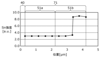
- FIG. FIG. 20 is a graph showing the Sn intensity distribution obtained by EDX (Energy Dispersive X-ray Spectroscopy) analysis on a straight line along the thickness direction of the first bonding region according to Embodiment 2.
- 21 is a graph showing the Sn intensity distribution obtained by EDX analysis on a straight line along the thickness direction of the second bonding region according to Embodiment 2.
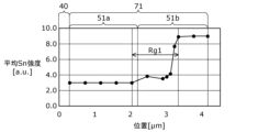
- FIG. FIG. 22 is a graph showing the average Sn intensity distribution obtained by EDX analysis in the region along the thickness direction of the first bonding region according to the second embodiment.
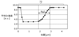
- FIG. 23 is a graph showing distribution of average Sn intensity obtained by EDX analysis in a region along the thickness direction of the second bonding region according to the second embodiment.
- each figure is a schematic diagram and is not necessarily strictly illustrated. Therefore, the scales and the like are not always the same in each drawing.
- symbol is attached
- the terms “upper” and “lower” do not refer to the upward direction (vertically upward) and the downward direction (vertically downward) in absolute spatial recognition, but are based on the stacking order in the stacking structure. It is used as a term defined by a relative positional relationship. Also, the terms “above” and “below” are used not only when two components are spaced apart from each other and there is another component between the two components, but also when two components are spaced apart from each other. It also applies when they are arranged in contact with each other.
- Embodiment 1 A semiconductor light emitting device according to Embodiment 1 will be described.
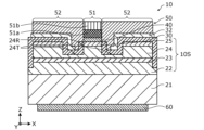
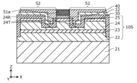
- FIG. 1 and 2 are a schematic plan view and a cross-sectional view, respectively, showing the overall configuration of a semiconductor light emitting device 10 according to this embodiment.
- FIG. 2 shows a cross section taken along line II-II of FIG.
- Each figure shows an X-axis, a Y-axis, and a Z-axis that are orthogonal to each other.
- the X, Y, and Z axes are a right-handed Cartesian coordinate system.
- the stacking direction of the semiconductor light emitting devices 10 is parallel to the Z-axis direction, and the main emission direction of light (laser light in this embodiment) is parallel to the Y-axis direction.
- the semiconductor light emitting device 10 includes a semiconductor laminate 10S, and emits light from an end face 10F (see FIG. 1) in a direction perpendicular to the lamination direction (that is, the Z-axis direction) of the semiconductor laminate 10S. emit.
- semiconductor light emitting device 10 is a nitride semiconductor laser device having two facets 10F and 10R forming a resonator.
- the end surface 10F is a front end surface that emits laser light
- the end surface 10R is a rear end surface having a higher reflectance than the end surface 10F.
- the reflectances of the end faces 10F and 10R are 6% and 98%, respectively.
- the semiconductor light emitting device 10 has a waveguide formed between the end face 10F and the end face 10R.
- the cavity length of semiconductor light emitting device 10 according to the present embodiment (that is, the distance between end face 10F and end face 10R) is approximately 1000 ⁇ m.
- the semiconductor light emitting device 10 emits blue-violet light having a peak wavelength in the 405 nm band, for example.
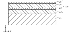
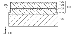
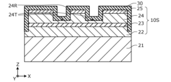
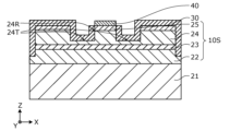
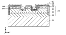
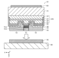
- the semiconductor light emitting device 10 includes a substrate 21, a semiconductor laminate 10S, an insulating layer 30, an adhesion assisting layer 32, a contact electrode 40, a pad layer 50, and an N-side electrode 60. Prepare.
- the substrate 21 is a plate-shaped member that serves as a base for the semiconductor light emitting device 10 .
- substrate 21 is an N-type GaN substrate.
- the semiconductor laminate 10S is a laminate containing a nitride semiconductor.
- the semiconductor laminate 10S has a plurality of semiconductor layers laminated in the lamination direction (that is, the Z-axis direction in each figure).
- the semiconductor stack 10S has an N-side semiconductor layer 22, an active layer 23, a P-side semiconductor layer 24, and a contact layer 25. As shown in FIG.
- the N-side semiconductor layer 22 is an example of a first conductivity type first semiconductor layer arranged above the substrate 21 and below the active layer 23 .
- the N-side semiconductor layer 22 contains a nitride semiconductor.
- the N-side semiconductor layer 22 includes an N-type cladding layer having a lower refractive index than the active layer 23 .
- the N-side semiconductor layer 22 is, for example, an N-type AlGaN layer. Note that the N-side semiconductor layer 22 may include layers other than the N-type clad layer.
- the N-side semiconductor layer 22 may include, for example, a buffer layer, an optical guide layer, and the like.
- the active layer 23 is a light-emitting layer arranged above the N-side semiconductor layer 22 .
- active layer 23 contains a nitride semiconductor and has a quantum well structure.
- the active layer 23 may have a single quantum well or multiple quantum wells.
- the active layer 23 has a plurality of barrier layers made of InGaN and a plurality of well layers made of InGaN.
- the P-side semiconductor layer 24 is an example of a second conductivity type second semiconductor layer arranged above the active layer 23 .
- the P-side semiconductor layer 24 contains a nitride semiconductor.
- the P-side semiconductor layer 24 includes a P-type cladding layer having a lower refractive index than the active layer 23 .
- the P-side semiconductor layer 24 is, for example, a P-type AlGaN layer.
- the P-side semiconductor layer 24 may include layers other than the P-type clad layer.
- the P-side semiconductor layer 24 may include, for example, an optical guide layer, an electron barrier layer, and the like. Also, the P-side semiconductor layer 24 may have a superlattice structure.
- a ridge 24 ⁇ /b>R is formed in the P-side semiconductor layer 24 .
- the ridge 24R is a portion of the P-side semiconductor layer 24 that protrudes in the Z-axis direction and extends in the Y-axis direction.
- two grooves 24T are formed along the ridge 24R and extend in the Y-axis direction.
- the ridge width (that is, the dimension of the ridge 24R in the X-axis direction) is approximately 30 ⁇ m.
- the dotted lines in FIG. 1 correspond to the positions of the side surfaces (not visible from the top surface) of the grooves 24T.
- the contact layer 25 is a layer arranged above the P-side semiconductor layer 24 and in ohmic contact with the contact electrode 40 .
- the contact layer 25 is a P-type GaN layer.
- the insulating layer 30 is a layer that is arranged between the semiconductor laminate 10S and the pad layer 50 and has electrical insulation.
- the insulating layer 30 has an opening (or slit) at a position corresponding to the upper surface of the ridge 24R.
- the insulating layer 30 is arranged in a region of the upper surface of the P-side semiconductor layer 24 other than the upper surface of the ridge 24R.
- the insulating layer 30 may be arranged on a part of the upper surface of the ridge 24R.
- the material forming the insulating layer 30 is not particularly limited as long as it is an insulating material.
- the insulating layer 30 is made of SiO 2 .
- the adhesion auxiliary layer 32 is a layer arranged above the insulating layer 30 .
- the adhesion auxiliary layer 32 is arranged between the insulating layer 30 and the pad layer 50 and has a function of enhancing adhesion between the pad layer 50 and the insulating layer 30 .
- the adhesion auxiliary layer 32 has openings (or slits) at positions corresponding to the openings of the insulating layer 30 .
- the opening of the insulating layer 30 is arranged inside the opening of the adhesion auxiliary layer 32 when the substrate 21 is viewed from above.
- the adhesion auxiliary layer 32 may contain at least one of Ti and Cr.
- the adhesion assisting layer 32 contains Ti and the insulating layer 30 is an oxide, the adhesion between the adhesion assisting layer 32 and the insulating layer 30 can be further enhanced. This is because when the insulating layer 30 is an oxide, the adhesion assisting layer 32 made of a metal film is also made of a material that easily forms an oxide, so that the insulating layer 30 is strongly bonded. In this embodiment, the adhesion assisting layer 32 has a laminated structure including a Ti film arranged on the insulating layer 30 and a Pt film arranged on the Ti film.
- the contact electrode 40 is an electrode arranged above the semiconductor laminate 10S.
- the contact electrode 40 faces the contact layer 25 above the contact layer 25 and contacts the contact layer 25 .
- the contact electrode 40 is arranged above the ridge 24R.
- the contact electrode 40 is, for example, a single layer film or multilayer film formed of at least one of Ag, Ni, Pd, Cr, and Pt, indium tin oxide (ITO; Indium Tin Oxide), indium zinc oxide (IZO; Indium Zinc Oxide), zinc oxide (ZnO; Zinc Oxide), or a transparent conductive film made of a transparent metal oxide such as InGaZnO x (IGZO).
- the contact electrode 40 has a Pd layer in contact with the contact layer 25 and a Pt layer arranged above the Pt layer.
- the pad layer 50 is a conductive layer arranged above the contact electrode 40 and in contact with the contact electrode 40 .
- the pad layer 50 contains Au.
- the pad layer 50 is an Au layer with a thickness of approximately 4 ⁇ m. A detailed configuration of the pad layer 50 will be described later.
- the N-side electrode 60 is a conductive layer arranged on the lower surface of the substrate 21 (that is, the main surface of the substrate 21 opposite to the main surface on which the semiconductor laminate 10S is arranged).
- the N-side electrode 60 is, for example, a single layer film or a multilayer film made of at least one of Cr, Ti, Ni, Pd and Pt, and a pad layer made of Au is formed on the N-side electrode 60.
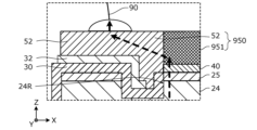
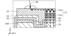
- the pad layer 50 has a contact region 51 and an external region 52. As shown in FIG. 2, the pad layer 50 has a contact region 51 and an external region 52. As shown in FIG.
- the contact region 51 is a region of the pad layer 50 arranged above the region where the pad layer 50 and the contact electrode 40 are in contact with each other.
- the contact region 51 includes a first layer 51a arranged above the region where the pad layer 50 and the contact electrode 40 are in contact, and a second layer 51b arranged above the first layer 51a and in contact with the first layer 51a.
- the insulating layer 30 is not arranged in the region between the semiconductor stacked body 10S and the first layer 51a among the regions between the semiconductor stacked body 10S and the pad layer 50 .
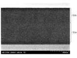
- FIG. 3 is a transmission electron microscope (TEM) photograph showing the crystal shape of contact region 51 according to the present embodiment.
- FIG. 3 shows the shape of crystal grains in a cross section parallel to the stacking direction of the contact region 51 .
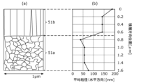
- FIG. 4 is a diagram showing the shape of crystal grains of contact region 51 according to the present embodiment.
- FIG. 4 shows a schematic diagram (a) of the grain boundary in the cross section corresponding to the TEM photograph shown in FIG. 3, and a graph (b) showing the distribution of the average grain size in the stacking direction.
- the contact electrode 40 shows the average grain size in the direction parallel to the main surface of the contact electrode 40 (that is, the direction parallel to the XY plane in each figure).
- the direction parallel to the main surface of the contact electrode 40 is also referred to as “horizontal direction”
- the direction perpendicular to it is also referred to as “vertical direction”.
- the first layer 51a is an Au layer having a thickness of about 0.9 ⁇ m, and as shown in the schematic diagrams (a) of FIGS. is a so-called granular grain having an aspect ratio of 0.5 to 2 in the horizontal and vertical directions.
- the second layer 51b is an Au layer having a thickness of about 0.7 ⁇ m, and as shown in the schematic diagrams (a) of FIGS. 3 and 4, the Au crystal grains in the second layer 51b are columnar. Each crystal in the second layer 51b extends in the stacking direction (that is, the Z-axis direction in each figure). In the horizontal direction, the average grain size of Au (that is, the average crystal grain size) in the second layer 51b is larger than the average grain size of Au in the first layer.
- the average grain size of Au in the first layer 51a is approximately 60 nm
- the average grain size of Au in the second layer 51b is approximately 150 nm.
- the electrical resistivity of the second layer 51b is lower than that of the first layer 51a in the horizontal direction.
- the average value of the average grain size of Au in the first layer 51a when the direction is not specified is about 60 nm, and the average value when the direction of the average grain size of Au in the second layer 51b is not specified is about 320 nm. be.
- the average value of the average particle size when the direction is not specified is also simply referred to as the "average particle size”.
- a method for measuring the average grain size of Au will be described later. As described above, since the average grain size of Au in the second layer 51b is larger than the average grain size in the first layer 51a, the electrical resistivity of the second layer 51b is lower than that of the first layer 51a.
- An external region 52 shown in FIG. 2 is a region of the pad layer 50 that is arranged above the insulating layer 30 .
- the external region 52 has a region that is directly connected (that is, contacts) with the insulating layer 30 and a region that is connected to the insulating layer 30 via the adhesion assisting layer 32 .
- the shape of the Au crystal grains in the outer region 52 is more random than in the first layer 51a.
- the average grain size of Au in the outer region 52 is larger than the average grain size of Au in the first layer 51a and smaller than the average grain size of Au in the second layer 51b. In this embodiment, the average grain size of Au in the outer region 52 is approximately 100 nm.
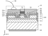
- FIG. 5 is a diagram showing an example of a current supply mode of the semiconductor light emitting device 10 according to this embodiment.
- a mode in which a wire 90 is connected to the pad layer 50 by bonding can be considered.
- the wire 90 is a conductive linear member and contains, for example, Au as a conductive material.
- the wire 90 is arranged on the upper surface of the pad layer 50 in a region other than above the ridge 24R of the semiconductor light emitting device 10, that is, in the external region 52. As shown in FIG. As a result, damage due to bonding to the ridge 24R and the layers positioned above and below the ridge 24R can be suppressed.
- the shape of the Au crystal grains in the external region 52 is more random than in the first layer 51a, and the average grain size of Au is larger than the average grain size of Au in the first layer 51a. Therefore, the hardness of the outer region 52 is lower than that of the first layer 51a. Therefore, by bonding the wire 90 to the external region 52, damage due to bonding to the semiconductor stacked body 10S can be suppressed.
- FIG. 6 is a diagram showing an outline of current paths in the pad layer 950 of the semiconductor light emitting device of the comparative example.
- FIG. 7 is a diagram showing an outline of current paths in the pad layer 50 according to the present embodiment. 6 and 7 show regions corresponding to the dashed frame shown in FIG. In FIGS. 6 and 7, outlines of electron movement paths are indicated by dashed arrows.
- the nitride semiconductor light emitting device of the comparative example shown in FIG. 6 is different from the semiconductor light emitting device 10 according to the present embodiment in the configuration of the pad layer 950, but is the same in other configurations.
- a pad layer 950 of the comparative example has a contact region 951 and an external region 52 .
- the contact region 951 of the comparative example has the same crystal grain shape as the first layer 51a of the contact region 51 according to the present embodiment. That is, the Au crystal grains in the contact region 951 of the comparative example are granular. Also, the average grain size of Au in the contact region 951 of the comparative example is approximately 60 nm.
- the electrical resistivity in the contact region 951 is relatively large. For this reason, as shown in FIG. 6, in the semiconductor light emitting device of the comparative example, electrons move along a short path passing through the contact region 951 . In other words, the current path concentrates in the region near the end of the ridge 24R that is closer to the bonding position of the wire 90 . Accordingly, in the semiconductor light emitting device of the comparative example, the light emission intensity distribution in the width direction of the ridge 24R is uneven, so that the active layer 23 tends to deteriorate near the peak position of the light emission intensity.
- the contact region 51 of the pad layer 50 has the second layer 51b arranged above the first layer 51a. Since the average grain size of Au in the horizontal direction in the second layer 51b is larger than the average grain size in the horizontal direction of Au in the first layer 51a, the electrical resistivity in the horizontal direction of the second layer 51b is equal to that of the first layer 51a. smaller than the electrical resistivity in the horizontal direction. That is, according to the semiconductor light emitting device 10 according to the present embodiment, the electrical resistance of the electrode including the pad layer 50 can be made lower than the electrical resistance of the electrode of the comparative example. This makes it easier for electrons to move horizontally in the second layer 51b. Therefore, as shown in FIG.
- the current paths can be dispersed in the width direction of the ridge 24R. That is, in the semiconductor light emitting device 10 according to the present embodiment, the light emission intensity distribution in the width direction of the ridge 24R can be made uniform. Therefore, the progress of local deterioration of the active layer 23 can be suppressed.
- the electric resistivity in the stacking direction of the second layer 51b can also be reduced. Therefore, the electrical resistance in the pad layer 50 can be further reduced.
- the electrical resistance of the electrodes can be reduced.
- FIG. 8 is a diagram for explaining the method of measuring the average particle size.
- a focused ion beam FIB
- SIM image Scanning Ion Microscopy image
- FIG. 9 to 16 are cross-sectional views showing respective steps of the method for manufacturing semiconductor light emitting device 10 according to the present embodiment. 9-16 show cross-sections similar to FIG.
- a substrate 21 is prepared.
- a wafer (GaN substrate) made of N-type GaN is prepared as the substrate 21 .
- an N-side semiconductor layer 22, an active layer 23, a P-side semiconductor layer 24, and a contact layer 25 are sequentially laminated on the substrate 21 by an epitaxial growth technique based on the MOCVD (Metal Organic Chemical Vapor Deposition) method. .
- MOCVD Metal Organic Chemical Vapor Deposition
- element isolation grooves 10D are formed for separating the semiconductor light emitting elements 10 into individual pieces.
- the element isolation grooves 10D are formed at positions corresponding to both ends of the semiconductor light emitting element 10 in the X-axis direction.
- the element isolation trench 10D reaches the inside of the N-side semiconductor layer 22 from the upper surface of the semiconductor stacked body 10S.
- a method for forming the isolation trench 10D is not particularly limited.
- the element isolation trench 10D may be formed using, for example, a photolithography technique and etching, or may be formed by laser processing.
- a ridge 24R is formed.
- the ridge 24R is formed by forming two grooves 24T in the semiconductor stacked body 10S. Each of the two grooves 24T reaches the inside of the P-side semiconductor layer 24 from the upper surface of the semiconductor stacked body 10S.
- a method for forming the isolation trench 10D is not particularly limited.
- the element isolation trench 10D is formed using photolithography and etching, for example.
- the insulating layer 30 is formed on the upper surface of the semiconductor stacked body 10S.
- a SiO 2 film is formed as the insulating layer 30 by plasma CVD (Chemical Vapor Deposition) or the like. Thereby, an insulating layer 30 made of amorphous SiO 2 is formed.
- the contact electrode 40 is formed on the contact layer 25 of the ridge 24R.
- a Pd layer and a Pt layer are formed as the contact electrode 40 .
- the contact electrode 40 is formed only above the ridge 24R using, for example, photolithography and vapor deposition.
- an adhesion auxiliary layer 32 is formed. Specifically, an adhesion assisting layer 32 made of a Ti film and a Pt film is formed on the insulating layer 30 using a photolithography technique and a vapor deposition method. Since the insulating layer 30 is amorphous SiO 2 , the adhesion assisting layer 32 has a more random grain shape than the Ti film and Pt film formed on the single crystal.
- part of the pad layer 50 is formed. Specifically, the temperature of the substrate 21 is maintained at about 100° C., and an Au film is formed over the contact electrodes 40 and the insulating layer 30 by vapor deposition. As a result, a first layer 51 a having granular and small crystal grains is formed on the contact electrode 40 . On the other hand, part of the outer region 52 is formed on the insulating layer 30 and the adhesion assisting layer 32 . Since the insulating layer 30 is amorphous SiO 2 , the outer region 52 formed on the insulating layer 30 has the shape of random crystal grains and becomes an Au film having many defects such as intergranular voids.
- the adhesion auxiliary layer 32 has the same random crystal grain shape as the insulating layer 30, the external region 52 formed on the adhesion auxiliary layer 32 also has the random crystal grain shape and the intergranular voids. It becomes an Au film having many defects such as.
- the rest of the pad layer 50 is formed. Specifically, after forming a portion of the pad layer 50 shown in FIG. 15, the formation is interrupted and the temperature of the substrate 21 is once lowered to about 50.degree. Subsequently, the formation of the Au film is restarted. At this time, the temperature of the substrate 21 may rise as the Au deposition progresses. Thereby, Au is epitaxially grown on the first layer 51a. As a result, the second layer 51b having columnar crystal grains and having an average grain size of Au in the horizontal direction larger than the average grain size of Au in the horizontal direction in the first layer 51a can be formed. In particular, when the contact electrode 40 is made of Pd, the average grain size of the columnar crystal grains can be maximized.
- an N-side electrode 60 is formed on the bottom surface of the substrate 21. Then, as shown in FIG. Specifically, the N-side electrode 60 is formed by sequentially forming a Ti film, a Pt film, and an Au film using photolithography and vapor deposition.
- the semiconductor light emitting device 10 according to the present embodiment can be manufactured by the manufacturing method as described above.
- a light-emitting module and a method for manufacturing the same according to Embodiment 2 will be described.
- a light-emitting module according to the present embodiment is a module manufactured using the semiconductor light-emitting device according to the first embodiment.
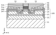
- FIG. 17 is a schematic cross-sectional view showing the overall configuration of light-emitting module 12 according to this embodiment.
- the light emitting module 12 includes a semiconductor light emitting element 110 and a base 80.
- the light emitting module 12 is a module obtained by junction-down mounting the semiconductor light emitting device 10 according to Embodiment 1 on the base 80 . A method for manufacturing the light emitting module 12 will be described later.
- the base 80 is a member to which the semiconductor light emitting device 110 is bonded.
- base 80 is a submount on which semiconductor light emitting device 110 is mounted.
- the base 80 has a rectangular plate shape.
- a ceramic substrate, a polycrystalline substrate, a single crystal substrate, or the like made of a material such as alumina, AlN, SiC, or diamond can be used.
- the base 80 is not limited to a submount.
- the base 80 may be a mounting substrate on which the semiconductor light emitting device 110 is mounted.
- a semiconductor light emitting device 110 includes a substrate 21, a semiconductor laminate 10S, a contact electrode 40, an adhesion auxiliary layer 32, a bonding layer 70, and an N-side electrode 60.
- the semiconductor light emitting device 110 is different from the semiconductor light emitting device 10 according to Embodiment 1 in that it includes a bonding layer 70 instead of the pad layer 50, and is otherwise the same.
- the contact electrode 40 according to the present embodiment is arranged between the semiconductor laminate 10S and the base 80. As shown in FIG.
- the insulating layer 30 according to the present embodiment is arranged between the semiconductor stacked body 10S and the bonding layer 70 .
- the bonding layer 70 is a layer that is bonded to the contact electrode 40 of the semiconductor light emitting device 110 and the base 80 and contains AuSn.
- the bonding layer 70 has a first bonding region 71 arranged at a position facing the region where the bonding layer 70 and the contact electrode 40 are in contact, and a second bonding region 72 arranged at a position facing the insulating layer 30.
- the adhesion auxiliary layer 32 is arranged between the second bonding region 72 and the insulating layer 30 .
- the bonding layer 70 bonds the contact electrode 40 , the insulating layer 30 , the adhesion auxiliary layer 32 and the base 80 .
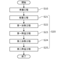
- FIG. 18 is a flow chart showing the flow of the method for manufacturing the light emitting module 12 according to this embodiment.
- FIG. 19 is a schematic cross-sectional view illustrating a preparation process for light-emitting module 12 according to this embodiment.
- the semiconductor light emitting device 10 according to Embodiment 1 and the base 80 are prepared (preparation step S10 in FIG. 18).
- the bonding material 56 is arranged on one main surface of the base 80 .
- the bonding material 56 is a member that bonds the base 80 and the pad layer 50 of the semiconductor light emitting device 10 in the bonding step S20 described later.
- the bonding material 56 is solder containing AuSn.
- the semiconductor light emitting device 10 is bonded to the base 80 using a bonding material 56 containing AuSn (bonding step S20).
- the bonding step S20 includes an arrangement step S21, a first heating step S22, a first cooling step S23, a second heating step S24, and a second cooling step S25.
- the semiconductor light emitting device 10 is arranged on the base 80 (arrangement step S21). Specifically, the semiconductor light emitting device 10 is moved toward the base 80 with the pad layer 50 of the semiconductor light emitting device 10 shown in FIG. 19 facing the bonding material 56 arranged on the base 80, The pad layer 50 of the semiconductor light emitting device 10 is brought into contact with the bonding material 56 arranged on the base 80 .
- the base 80 is heated to a first peak temperature T1 higher than the melting point Tm of the bonding material 56 to melt the bonding material 56 (first heating step S22).
- the base 80 is heated by placing the base 80 on a heater and increasing the temperature of the heater.
- this first heating step S ⁇ b>22 before the temperature of the base 80 reaches the melting point Tm of the bonding material 56 , by starting to apply a load to the semiconductor light emitting device 10 , the semiconductor light emitting device 10 is heated to the base 80 . press against.
- the bonding material 56 melts, the contact area between the surface of the semiconductor light emitting element 10 facing the bonding material 56 and the bonding material 56 can be increased. In other words, formation of voids between the semiconductor light emitting element 10 and the bonding material 56 can be suppressed.
- the temperature of the base 80 is lowered to the switching temperature Tv which is lower than the melting point Tm of the bonding material 56 (first temperature lowering step S23).
- first temperature lowering step S23 before the temperature of the base 80 reaches the melting point Tm of the bonding material 56, the application of the load to the semiconductor light emitting device 10 is stopped.
- the temperature at which the application of the load is stopped does not necessarily have to be higher than the melting point Tm, and may be lower than the melting point Tm.
- the base 80 is heated to a second peak temperature T2 higher than the melting point Tm of the bonding material 56 to melt the bonding material 56 again (second heating step S24).
- the first peak temperature T1, the second peak temperature T2, and the melting point Tm of the bonding material 56 satisfy the relationship Tm ⁇ T1 ⁇ T2.
- the temperature of the base 80 is lowered to a temperature below the melting point Tm of the bonding material 56 (second temperature lowering step S25).
- the temperature of the base 80 is lowered to the temperature before performing the first heating step S22 (that is, the standby temperature).
- a load may or may not be applied to the semiconductor light emitting device 10 in the second heating step S60 and the second cooling step S70.
- the bonding layer 70 is formed by integrating the pad layer 50 of the semiconductor light emitting element 10 and the bonding material 56 together. Specifically, Sn contained in the bonding material 56 diffuses into the pad layer 50 made of Au to form a bonding layer 70 containing AuSn.
- the bonding layer 70 of the light emitting module 12 is a layer in which the pad layer 50 of the semiconductor light emitting device 10 according to Embodiment 1 and the bonding material 56 are integrated.
- the first bonding region 71 and the second bonding region 72 of the bonding layer 70 are regions corresponding to the contact region 51 and the external region 52 of the pad layer 50, respectively. That is, the contact region 51 and part of the bonding material 56 form the first bonding region 71 , and the external region 52 and another part of the bonding material 56 form the second bonding region 72 . Due to the difference in crystal grain shape between the contact region 51 and the external region 52 , the distribution of Sn differs between the first junction region 71 and the second junction region 72 .
- FIG. 20 and 21 show EDX (Energy 1 is a graph showing the Sn intensity distribution obtained by Dispersive X-ray Spectroscopy) analysis.
- 22 and 23 are graphs showing average Sn intensity distributions obtained by EDX analysis in regions along the thickness direction of the first bonding region 71 and the second bonding region 72 according to the present embodiment, respectively. is.
- the horizontal axis of each figure indicates the position in the thickness direction. As the numerical value on the horizontal axis increases, the position approaches the base 80, and as the numerical value on the horizontal axis decreases, the position approaches the semiconductor stack 10S.
- FIGS. 22 and 23 are the Sn intensities in the regions corresponding to the dashed-line frames R1 and R2 in FIG. 17, respectively.
- Broken-line frames R1 and R2 are regions each having a length in the thickness direction of the bonding layer 70 and a length in the X-axis direction of 5 ⁇ m.
- the Sn intensity and average Sn intensity in FIGS. 20 to 23 correspond to the Sn content and average content at each position in the bonding layer 70 in the thickness direction.
- the Sn content is high in the region of the first bonding region 71 that corresponds to the second layer 51b of the pad layer 50 .
- the Au crystals are granular, and the average grain size is , Sn is less likely to diffuse than the region corresponding to the second layer 51b. Therefore, as shown in FIGS. 20 and 22, the Sn content is low in the region of the first bonding region 71 that corresponds to the first layer 51a of the pad layer 50 . Therefore, as shown in FIG. 20 , the Sn content increases stepwise along a straight line along the thickness direction of the first junction region 71 as the distance from the contact electrode 40 increases. Further, as shown in FIG.
- the average Sn content of the first bonding region 71 gradually increases as the distance from the contact electrode 40 increases.
- the contact resistance between the contact layer 25 and the contact electrode 40 increases.
- the diffusion of Sn is suppressed by the region corresponding to the first layer 51a of the pad layer 50 in the first bonding region 71, so that the diffusion of Sn into the contact layer 25 can be suppressed. Therefore, an increase in contact resistance between the contact layer 25 and the contact electrode 40 can be suppressed. In other words, the electrical resistance of the electrodes including the contact electrode 40 and the bonding layer 70 of the semiconductor light emitting device 110 can be reduced.
- the average Sn content in the region closer to the contact electrode 40 than the center of the thickness direction of the first bonding region 71 in the first bonding region 71 is , less than the average Sn content in a region of the first junction region 71 farther from the contact electrode 40 than the center.
- the second bonding region 72 is a region corresponding to the outer region 52 having many defects such as intergranular voids of Au in the pad layer 50, Sn is likely to diffuse. Therefore, as shown in FIGS. 21 and 23, a large amount of Sn diffuses to the end portion of the second junction region 72 closer to the insulating layer 30 . Therefore, the bonding strength between the bonding layer 70 and the base 80 can be increased. Therefore, it is possible to prevent the semiconductor light emitting element 110 from detaching from the base 80 .
- the Sn content at the center of the second bonding region 72 in the thickness direction is less than the Sn content at both ends of the second bonding region 72 in the thickness direction.
- the reason why the average Sn content is high not only at the end portion on the base 80 side in the thickness direction of the second bonding region 72 but also at the end portion on the insulating layer 30 side is that the second bonding region 72 has a large Sn content. It is presumed that this is due to the presence of grain boundaries or defects in which Sn particularly easily diffuses locally.
- the average Sn content of the second bonding region 72 gradually increases as the distance from the insulating layer 30 increases. has a second transition region Rg2 that In this way, the second transition region Rg2 in which the average Sn content gradually increases in the second bonding region 72 can suppress a rapid change in the Sn content in the thickness method. Rapid changes in the coefficient of thermal expansion can be suppressed in the region where . Therefore, it is possible to suppress the breakage of the second bonding region 72 due to the temperature change.
- the average grain size of the first layer 51a and the second layer 51b of the pad layer 50 of the semiconductor light emitting device 10 according to Embodiment 1 is not limited to the values described above.
- the average grain size of Au in the first layer 51a may be 30 nm or more and 80 nm or less, and the average grain size of Au in the second layer 51b may be 120 nm or more and 200 nm or less.
- the average grain size of Au in the first layer 51a may be 30 nm or more and 80 nm or less, and the average grain size of Au in the second layer 51b may be 240 nm or more and 630 nm or less. .
- the thicknesses of the first layer 51a and the second layer 51b of the pad layer 50 were approximately the same, but the thickness of the first layer 51a and the second layer 51b
- the relative relationship of height is not limited to this.
- the second layer 51b may be thicker than the first layer 51a. As a result, the ratio of the second layer 51b having a low electrical resistivity in the pad layer 50 is increased, so that the electrical resistivity of the pad layer 50 can be reduced.
- the semiconductor light emitting device is a nitride semiconductor laser device
- the semiconductor light emitting device is not limited to a semiconductor laser device.
- the semiconductor light emitting device may be a superluminescent diode.
- the reflectance of the end surface of the semiconductor laminate included in the nitride semiconductor light-emitting device with respect to the emitted light from the semiconductor laminate may be 0.1% or less.
- Such a reflectance can be realized, for example, by forming an antireflection film made of a dielectric multilayer film or the like on the end face.
- the guided light reflected by the front end face is coupled again with the waveguide to form a guided light component.
- the semiconductor light emitting device may be a light emitting diode.
- the nitride semiconductor light emitting device and the like of the present disclosure can be applied, for example, as a light source for processing machines as a highly efficient light source.
- Reference Signs List 10 110 nitride semiconductor light emitting element 10D element separation groove 10F, 10R end face 10S semiconductor laminate 12 light emitting module 21 substrate 22 N-side semiconductor layer 23 active layer 24 P-side semiconductor layer 24R ridge 24T groove 25 contact layer 30 insulating layer 32 adhesion Auxiliary layer 40 Contact electrode 50 Pad layer 51 Contact region 51a First layer 51b Second layer 52 External region 56 Bonding material 60 N-side electrode 70 Bonding layer 71 First bonding region 72 Second bonding region 80 Base 90 Wire
Landscapes
- Engineering & Computer Science (AREA)
- Physics & Mathematics (AREA)
- Condensed Matter Physics & Semiconductors (AREA)
- General Physics & Mathematics (AREA)
- Microelectronics & Electronic Packaging (AREA)
- Power Engineering (AREA)
- Computer Hardware Design (AREA)
- Manufacturing & Machinery (AREA)
- Optics & Photonics (AREA)
- Electromagnetism (AREA)
- Led Devices (AREA)
- Electrodes Of Semiconductors (AREA)
- Internal Circuitry In Semiconductor Integrated Circuit Devices (AREA)
- Semiconductor Lasers (AREA)
Priority Applications (2)
| Application Number | Priority Date | Filing Date | Title |
|---|---|---|---|
| CN202280074625.5A CN118216052A (zh) | 2021-11-10 | 2022-10-31 | 半导体发光元件、发光模块及发光模块的制造方法 |
| US18/653,508 US20240282901A1 (en) | 2021-11-10 | 2024-05-02 | Semiconductor light-emitting element, light-emitting module, and method for manufacturing light-emitting module |
Applications Claiming Priority (2)
| Application Number | Priority Date | Filing Date | Title |
|---|---|---|---|
| JP2021-183532 | 2021-11-10 | ||
| JP2021183532A JP2023070990A (ja) | 2021-11-10 | 2021-11-10 | 半導体発光素子、発光モジュール、及び発光モジュールの製造方法 |
Related Child Applications (1)
| Application Number | Title | Priority Date | Filing Date |
|---|---|---|---|
| US18/653,508 Continuation US20240282901A1 (en) | 2021-11-10 | 2024-05-02 | Semiconductor light-emitting element, light-emitting module, and method for manufacturing light-emitting module |
Publications (1)
| Publication Number | Publication Date |
|---|---|
| WO2023085161A1 true WO2023085161A1 (ja) | 2023-05-19 |
Family
ID=86335930
Family Applications (1)
| Application Number | Title | Priority Date | Filing Date |
|---|---|---|---|
| PCT/JP2022/040764 Ceased WO2023085161A1 (ja) | 2021-11-10 | 2022-10-31 | 半導体発光素子、発光モジュール、及び発光モジュールの製造方法 |
Country Status (4)
| Country | Link |
|---|---|
| US (1) | US20240282901A1 (enExample) |
| JP (1) | JP2023070990A (enExample) |
| CN (1) | CN118216052A (enExample) |
| WO (1) | WO2023085161A1 (enExample) |
Cited By (1)
| Publication number | Priority date | Publication date | Assignee | Title |
|---|---|---|---|---|
| CN116683286A (zh) * | 2023-06-15 | 2023-09-01 | 厦门市三安光电科技有限公司 | 一种半导体激光器 |
Citations (6)
| Publication number | Priority date | Publication date | Assignee | Title |
|---|---|---|---|---|
| JP2006278463A (ja) * | 2005-03-28 | 2006-10-12 | Dowa Mining Co Ltd | サブマウント |
| JP2012227383A (ja) * | 2011-04-20 | 2012-11-15 | Showa Denko Kk | 半導体発光素子、電極構造および発光装置 |
| US20130062587A1 (en) * | 2011-09-13 | 2013-03-14 | Adesto Technologies Corp. | Resistive Switching Devices Having Alloyed Electrodes And Methods of Formation Thereof |
| JP2014038886A (ja) * | 2012-08-10 | 2014-02-27 | Toshiba Corp | 半導体装置及びその製造方法 |
| WO2019150825A1 (ja) * | 2018-02-01 | 2019-08-08 | パナソニックIpマネジメント株式会社 | 半導体装置 |
| US20210020595A1 (en) * | 2019-07-16 | 2021-01-21 | Nxp Usa, Inc. | Semiconductor dies having ultra-thin wafer backmetal systems, microelectronic devices containing the same, and associated fabrication methods |
-
2021
- 2021-11-10 JP JP2021183532A patent/JP2023070990A/ja active Pending
-
2022
- 2022-10-31 CN CN202280074625.5A patent/CN118216052A/zh active Pending
- 2022-10-31 WO PCT/JP2022/040764 patent/WO2023085161A1/ja not_active Ceased
-
2024
- 2024-05-02 US US18/653,508 patent/US20240282901A1/en active Pending
Patent Citations (6)
| Publication number | Priority date | Publication date | Assignee | Title |
|---|---|---|---|---|
| JP2006278463A (ja) * | 2005-03-28 | 2006-10-12 | Dowa Mining Co Ltd | サブマウント |
| JP2012227383A (ja) * | 2011-04-20 | 2012-11-15 | Showa Denko Kk | 半導体発光素子、電極構造および発光装置 |
| US20130062587A1 (en) * | 2011-09-13 | 2013-03-14 | Adesto Technologies Corp. | Resistive Switching Devices Having Alloyed Electrodes And Methods of Formation Thereof |
| JP2014038886A (ja) * | 2012-08-10 | 2014-02-27 | Toshiba Corp | 半導体装置及びその製造方法 |
| WO2019150825A1 (ja) * | 2018-02-01 | 2019-08-08 | パナソニックIpマネジメント株式会社 | 半導体装置 |
| US20210020595A1 (en) * | 2019-07-16 | 2021-01-21 | Nxp Usa, Inc. | Semiconductor dies having ultra-thin wafer backmetal systems, microelectronic devices containing the same, and associated fabrication methods |
Cited By (1)
| Publication number | Priority date | Publication date | Assignee | Title |
|---|---|---|---|---|
| CN116683286A (zh) * | 2023-06-15 | 2023-09-01 | 厦门市三安光电科技有限公司 | 一种半导体激光器 |
Also Published As
| Publication number | Publication date |
|---|---|
| JP2023070990A (ja) | 2023-05-22 |
| CN118216052A (zh) | 2024-06-18 |
| US20240282901A1 (en) | 2024-08-22 |
Similar Documents
| Publication | Publication Date | Title |
|---|---|---|
| US7892874B2 (en) | Nitride-based light-emitting device and method of manufacturing the same | |
| US8338844B2 (en) | Semiconductor light emitting apparatus having stacked reflective dielectric films | |
| JP5894293B2 (ja) | 半導体レーザダイオード | |
| JP6926205B2 (ja) | 半導体レーザーダイオード | |
| US20080179605A1 (en) | Nitride semiconductor light emitting device and method for fabricating the same | |
| US20080267238A1 (en) | Semiconductor laser diode element and method of manufacturing the same | |
| US9735314B2 (en) | Nitride semiconductor light emitting device | |
| JP2020524407A (ja) | 半導体レーザーダイオード | |
| WO2022079971A1 (ja) | 赤外led素子 | |
| WO2023085161A1 (ja) | 半導体発光素子、発光モジュール、及び発光モジュールの製造方法 | |
| JP4960777B2 (ja) | 端面発光型半導体レーザチップ | |
| US9287481B2 (en) | Vertical nitride semiconductor device and method for manufacturing same | |
| US20230335972A1 (en) | Semiconductor laser and semiconductor laser device | |
| WO2022019054A1 (ja) | 半導体レーザおよび半導体レーザ装置 | |
| TWI901722B (zh) | 半絕緣性InP基板的紅外LED元件 | |
| JP2008294421A (ja) | 半導体レーザ素子およびその製造方法 | |
| WO2025182842A1 (ja) | 半導体発光素子、及び、半導体発光素子の製造方法 | |
| CN119836719A (zh) | 半导体激光元件 | |
| JP2004088000A (ja) | 半導体レーザ素子の製造方法及び半導体レーザ素子 |
Legal Events
| Date | Code | Title | Description |
|---|---|---|---|
| 121 | Ep: the epo has been informed by wipo that ep was designated in this application |
Ref document number: 22892660 Country of ref document: EP Kind code of ref document: A1 |
|
| WWE | Wipo information: entry into national phase |
Ref document number: 202280074625.5 Country of ref document: CN |
|
| 122 | Ep: pct application non-entry in european phase |
Ref document number: 22892660 Country of ref document: EP Kind code of ref document: A1 |