WO2023074344A1 - 電力変換装置 - Google Patents
電力変換装置 Download PDFInfo
- Publication number
- WO2023074344A1 WO2023074344A1 PCT/JP2022/037822 JP2022037822W WO2023074344A1 WO 2023074344 A1 WO2023074344 A1 WO 2023074344A1 JP 2022037822 W JP2022037822 W JP 2022037822W WO 2023074344 A1 WO2023074344 A1 WO 2023074344A1
- Authority
- WO
- WIPO (PCT)
- Prior art keywords
- semiconductor module
- input terminal
- semiconductor
- conductive
- center line
- Prior art date
- Legal status (The legal status is an assumption and is not a legal conclusion. Google has not performed a legal analysis and makes no representation as to the accuracy of the status listed.)
- Ceased
Links
Images

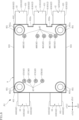
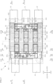
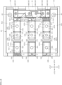

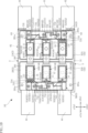






Classifications
-
- H—ELECTRICITY
- H02—GENERATION; CONVERSION OR DISTRIBUTION OF ELECTRIC POWER
- H02M—APPARATUS FOR CONVERSION BETWEEN AC AND AC, BETWEEN AC AND DC, OR BETWEEN DC AND DC, AND FOR USE WITH MAINS OR SIMILAR POWER SUPPLY SYSTEMS; CONVERSION OF DC OR AC INPUT POWER INTO SURGE OUTPUT POWER; CONTROL OR REGULATION THEREOF
- H02M7/00—Conversion of AC power input into DC power output; Conversion of DC power input into AC power output
- H02M7/42—Conversion of DC power input into AC power output without possibility of reversal
- H02M7/44—Conversion of DC power input into AC power output without possibility of reversal by static converters
- H02M7/48—Conversion of DC power input into AC power output without possibility of reversal by static converters using discharge tubes with control electrode or semiconductor devices with control electrode
- H02M7/53—Conversion of DC power input into AC power output without possibility of reversal by static converters using discharge tubes with control electrode or semiconductor devices with control electrode using devices of a triode or transistor type requiring continuous application of a control signal
- H02M7/537—Conversion of DC power input into AC power output without possibility of reversal by static converters using discharge tubes with control electrode or semiconductor devices with control electrode using devices of a triode or transistor type requiring continuous application of a control signal using semiconductor devices only, e.g. single switched pulse inverters
-
- H—ELECTRICITY
- H10—SEMICONDUCTOR DEVICES; ELECTRIC SOLID-STATE DEVICES NOT OTHERWISE PROVIDED FOR
- H10W—GENERIC PACKAGES, INTERCONNECTIONS, CONNECTORS OR OTHER CONSTRUCTIONAL DETAILS OF DEVICES COVERED BY CLASS H10
- H10W90/00—Package configurations
-
- H—ELECTRICITY
- H05—ELECTRIC TECHNIQUES NOT OTHERWISE PROVIDED FOR
- H05K—PRINTED CIRCUITS; CASINGS OR CONSTRUCTIONAL DETAILS OF ELECTRIC APPARATUS; MANUFACTURE OF ASSEMBLAGES OF ELECTRICAL COMPONENTS
- H05K7/00—Constructional details common to different types of electric apparatus
- H05K7/14—Mounting supporting structure in casing or on frame or rack
- H05K7/1422—Printed circuit boards receptacles, e.g. stacked structures, electronic circuit modules or box like frames
- H05K7/1427—Housings
- H05K7/1432—Housings specially adapted for power drive units or power converters
- H05K7/14329—Housings specially adapted for power drive units or power converters specially adapted for the configuration of power bus bars
-
- H—ELECTRICITY
- H10—SEMICONDUCTOR DEVICES; ELECTRIC SOLID-STATE DEVICES NOT OTHERWISE PROVIDED FOR
- H10W—GENERIC PACKAGES, INTERCONNECTIONS, CONNECTORS OR OTHER CONSTRUCTIONAL DETAILS OF DEVICES COVERED BY CLASS H10
- H10W70/00—Package substrates; Interposers; Redistribution layers [RDL]
- H10W70/40—Leadframes
- H10W70/421—Shapes or dispositions
-
- H—ELECTRICITY
- H10—SEMICONDUCTOR DEVICES; ELECTRIC SOLID-STATE DEVICES NOT OTHERWISE PROVIDED FOR
- H10W—GENERIC PACKAGES, INTERCONNECTIONS, CONNECTORS OR OTHER CONSTRUCTIONAL DETAILS OF DEVICES COVERED BY CLASS H10
- H10W72/00—Interconnections or connectors in packages
-
- H—ELECTRICITY
- H02—GENERATION; CONVERSION OR DISTRIBUTION OF ELECTRIC POWER
- H02M—APPARATUS FOR CONVERSION BETWEEN AC AND AC, BETWEEN AC AND DC, OR BETWEEN DC AND DC, AND FOR USE WITH MAINS OR SIMILAR POWER SUPPLY SYSTEMS; CONVERSION OF DC OR AC INPUT POWER INTO SURGE OUTPUT POWER; CONTROL OR REGULATION THEREOF
- H02M7/00—Conversion of AC power input into DC power output; Conversion of DC power input into AC power output
- H02M7/003—Constructional details, e.g. physical layout, assembly, wiring or busbar connections
-
- H—ELECTRICITY
- H10—SEMICONDUCTOR DEVICES; ELECTRIC SOLID-STATE DEVICES NOT OTHERWISE PROVIDED FOR
- H10W—GENERIC PACKAGES, INTERCONNECTIONS, CONNECTORS OR OTHER CONSTRUCTIONAL DETAILS OF DEVICES COVERED BY CLASS H10
- H10W40/00—Arrangements for thermal protection or thermal control
- H10W40/20—Arrangements for cooling
- H10W40/25—Arrangements for cooling characterised by their materials
- H10W40/255—Arrangements for cooling characterised by their materials having a laminate or multilayered structure, e.g. direct bond copper [DBC] ceramic substrates
-
- H—ELECTRICITY
- H10—SEMICONDUCTOR DEVICES; ELECTRIC SOLID-STATE DEVICES NOT OTHERWISE PROVIDED FOR
- H10W—GENERIC PACKAGES, INTERCONNECTIONS, CONNECTORS OR OTHER CONSTRUCTIONAL DETAILS OF DEVICES COVERED BY CLASS H10
- H10W70/00—Package substrates; Interposers; Redistribution layers [RDL]
- H10W70/40—Leadframes
- H10W70/464—Additional interconnections in combination with leadframes
-
- H—ELECTRICITY
- H10—SEMICONDUCTOR DEVICES; ELECTRIC SOLID-STATE DEVICES NOT OTHERWISE PROVIDED FOR
- H10W—GENERIC PACKAGES, INTERCONNECTIONS, CONNECTORS OR OTHER CONSTRUCTIONAL DETAILS OF DEVICES COVERED BY CLASS H10
- H10W70/00—Package substrates; Interposers; Redistribution layers [RDL]
- H10W70/40—Leadframes
- H10W70/481—Leadframes for devices being provided for in groups H10D8/00 - H10D48/00
-
- H—ELECTRICITY
- H10—SEMICONDUCTOR DEVICES; ELECTRIC SOLID-STATE DEVICES NOT OTHERWISE PROVIDED FOR
- H10W—GENERIC PACKAGES, INTERCONNECTIONS, CONNECTORS OR OTHER CONSTRUCTIONAL DETAILS OF DEVICES COVERED BY CLASS H10
- H10W70/00—Package substrates; Interposers; Redistribution layers [RDL]
- H10W70/60—Insulating or insulated package substrates; Interposers; Redistribution layers
-
- H—ELECTRICITY
- H10—SEMICONDUCTOR DEVICES; ELECTRIC SOLID-STATE DEVICES NOT OTHERWISE PROVIDED FOR
- H10W—GENERIC PACKAGES, INTERCONNECTIONS, CONNECTORS OR OTHER CONSTRUCTIONAL DETAILS OF DEVICES COVERED BY CLASS H10
- H10W90/00—Package configurations
- H10W90/701—Package configurations characterised by the relative positions of pads or connectors relative to package parts
-
- H—ELECTRICITY
- H10—SEMICONDUCTOR DEVICES; ELECTRIC SOLID-STATE DEVICES NOT OTHERWISE PROVIDED FOR
- H10W—GENERIC PACKAGES, INTERCONNECTIONS, CONNECTORS OR OTHER CONSTRUCTIONAL DETAILS OF DEVICES COVERED BY CLASS H10
- H10W90/00—Package configurations
- H10W90/811—Multiple chips on leadframes
Definitions
- the present disclosure relates to power converters.
- Patent Document 1 discloses a conventional semiconductor module (power module).
- the present disclosure has been conceived in view of the above circumstances, and an object thereof is to provide a power conversion device capable of more uniform inductance between a capacitor module and a plurality of semiconductor modules. do.
- a power conversion device includes a first semiconductor module, a second semiconductor module, and a third semiconductor module each having a semiconductor element having a switching function and an input terminal, the first semiconductor module, the second semiconductor module, and the a capacitor module connected to the input terminal of the third semiconductor module.
- the capacitor module has a capacitor main body, and a first bus bar, a second bus bar, and a third bus bar protruding from the capacitor main body.
- the input terminal of the first semiconductor module is connected to the first bus bar
- the input terminal of the second semiconductor module is connected to the second bus bar
- the input terminal of the third semiconductor module is connected to the third bus bar. is connected.
- a third centerline intersects the capacitor body.
- a first angle formed by the first center line and the second center line and a second angle formed by the second center line and the third center line are equal to each other.
- the lengths of the first busbar, the second busbar and the third busbar are equal to each other.
- the semiconductor module of the present disclosure it is possible to provide a power converter capable of making the inductance between the capacitor module and the plurality of semiconductor modules more uniform.
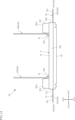
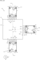
- FIG. 1 is a plan view showing the power converter according to the first embodiment.
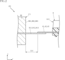
- FIG. 2 is an enlarged cross-sectional view of a main part taken along line II-II of FIG.
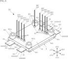
- FIG. 3 is a perspective view of the semiconductor module according to the first embodiment.
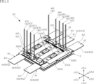
- FIG. 4 is a perspective view of FIG. 3 with the sealing resin, the resin portion, and the resin-filled portion omitted.
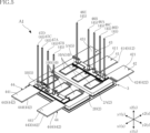
- FIG. 5 is a perspective view of FIG. 4 with the conductive member omitted.
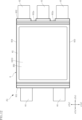
- 6 is a plan view showing the semiconductor module according to the first embodiment.
- FIG. FIG. 7 is a diagram showing the sealing resin, the resin portion, and the resin-filled portion in the plan view of FIG. 6 with imaginary lines.
- FIG. 8 is a partial enlarged view enlarging a part of FIG.
- FIG. 9 is a partially enlarged view enlarging a part of FIG.
- FIG. 10 is a diagram showing a part of the conductive member in phantom lines in the plan view of FIG. 11 is a front view showing the semiconductor module according to the first embodiment;
- FIG. 12 is a bottom view showing the semiconductor module according to the first embodiment;
- FIG. 13 is a left side view showing the semiconductor module according to the first embodiment;
- FIG. 14 is a right side view showing the semiconductor module according to the first embodiment;
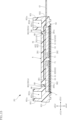
- FIG. 15 is a cross-sectional view along line XV-XV in FIG. 7.
- FIG. 16 is a cross-sectional view taken along line XVI--XVI of FIG.
- FIG. 17 is a partially enlarged view enlarging a part of FIG. 16.
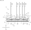
- FIG. FIG. 18 is a cross-sectional view along line XVIII-XVIII in FIG. 19 is a cross-sectional view along line XIX-XIX in FIG. 7.
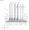
- FIG. 20 is a cross-sectional view along line XX-XX of FIG. 7.
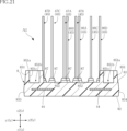
- FIG. 21 is a cross-sectional view taken along line XXI-XXI of FIG. 7.
- FIG. FIG. 22 is a circuit configuration example of the semiconductor module according to the first embodiment.
- FIG. 23 is a plan view showing a first modification of the power converter according to the first embodiment.
- FIG. 24 is a plan view showing a second modification of the power converter according to the first embodiment.
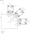
- FIG. 25 is a plan view showing the power converter according to the second embodiment.
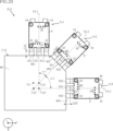
- FIG. 26 is a plan view showing the power converter according to the third embodiment.
- First embodiment: 1 and 2 show a power converter according to a first embodiment of the present disclosure.
- the power converter B1 of this embodiment includes a first semiconductor module A11, a second semiconductor module A12, a third semiconductor module A13, and a capacitor module C1.
- the functions and applications of the power conversion device of the present disclosure are not limited at all, and the power conversion device B1 of the present embodiment is configured as a so-called inverter.
- the z direction is an example of the "axial direction”
- the x direction is an example of the "radial direction”
- the ⁇ direction is an example of the "circumferential direction”.
- Capacitor module C1 functions, for example, as a smoothing capacitor provided in a power supply circuit to the first semiconductor module A11, the second semiconductor module A12, and the third semiconductor module A13.
- the capacitor module C ⁇ b>1 of this embodiment has a capacitor main body 90 , multiple first bus bars 911 , 912 , 913 , multiple second bus bars 921 , 922 , 923 and multiple third bus bars 931 , 932 , 933 .
- the capacitor main body 90 is a part that functions as a capacitor of the capacitor module C1.
- a specific configuration of the capacitor body portion 90 is not limited at all.
- Capacitor main body 90 suitably has, for example, a capacitor element (not shown) and a wiring conductor (not shown).
- the type and structure of the capacitor element are not limited at all, and conventionally known various capacitor elements can be used.
- the center point Oz in the drawing is the center of the capacitor main body 90 when viewed in the z direction.
- the center point Oz may be the geometric center of the capacitor main body 90 when viewed in the z direction, or may be the center of gravity.
- the capacitor body 90 of this embodiment has a first surface 901 , a second surface 902 and a third surface 903 .
- the first surface 901 is a surface perpendicular to a center line OL1, which will be described later.
- the second surface 902 is a surface perpendicular to the centerline OL2, which will be described later.
- the third surface 903 is a surface perpendicular to the center line OL3, which will be described later.
- the angles formed by the first surface 901, the second surface 902 and the third surface 903 are not limited at all. In the illustrated example, the angle between the first surface 901 and the second surface 902 is 45°. Also, the angle formed by the second surface 902 and the third surface 903 is 45°.
- the first surface 901, the second surface 902 and the third surface 903 are orthogonal to a radius extending in the r direction through the center point Oz when viewed in the z direction. Also, the first surface 901, the second surface 902 and the third surface 903 are adjacent to each other.
- the plurality of first busbars 911, 912, 913, the plurality of second busbars 921, 922, 923 and the plurality of third busbars 931, 932, 933 are connected to the first semiconductor module A11, the second semiconductor module A12, and the third semiconductor module.
- A13 are individually connected, each conducting a capacitor element.
- the first bus bars 911, 912, 913 protrude from the first surface 901 in the r direction when viewed in the z direction.
- the first bus bars 911, 912, and 913 are arranged so that the first bus bar 912 and the first bus bar 913 are separated from each other in the ⁇ direction with the first bus bar 911 interposed therebetween when viewed in the z direction.
- the second bus bars 921, 922, 923 protrude from the second surface 902 in the r direction when viewed in the z direction.
- the second bus bars 921, 922, and 923 are arranged so that the second bus bar 922 and the second bus bar 923 are separated from each other in the ⁇ direction with the second bus bar 921 interposed therebetween when viewed in the z direction.
- the third bus bars 931, 932, 933 protrude from the third surface 903 in the r direction when viewed in the z direction.
- the third bus bars 931, 932, and 933 are arranged so that the third bus bar 932 and the third bus bar 933 are separated from each other in the ⁇ direction with the third bus bar 931 interposed therebetween when viewed in the z direction.
- Each of the first semiconductor module A11, the second semiconductor module A12, and the third semiconductor module A13 includes a plurality of 41, 42, 43, a plurality of output terminals 44, a plurality of control terminals 45, and a sealing resin 8.
- a specific configuration example of the plurality of 41, 42, 43, the plurality of output terminals 44, the plurality of control terminals 45, and the sealing resin 8 will be described later.
- a plurality of 41 , 42 , 43 protrude from the sealing resin 8 to one side in the r direction.
- a plurality of output terminals 44 protrude from the sealing resin 8 to the other side in the r direction.
- a plurality of control terminals 45 protrude from the sealing resin 8 in the z direction.
- the input terminal 41 of the first semiconductor module A11 is connected to the first busbar 911, the input terminal 42 is connected to the first busbar 912, and the input terminal 43 is connected to the first busbar 913.
- the input terminal 41 of the second semiconductor module A12 is connected to the second bus bar 921, the input terminal 42 is connected to the second bus bar 922, and the input terminal 43 is connected to the second bus bar 923.
- the input terminal 41 of the third semiconductor module A13 is connected to the third bus bar 931, the input terminal 42 is connected to the third bus bar 932, and the input terminal 43 is connected to the third bus bar 933.
- the method of connecting these input terminals and the bus bar is not limited in any way, and various conventionally known methods such as fastening using bolts or the like, joining using joining material, welding or the like, engagement, fitting, etc. can be used. can be used.
- the centerline OL1 is the centerline of the first semiconductor module A11 when viewed in the z direction.
- Center line OL1 is a line that passes through, for example, the geometric center or the center of gravity of sealing resin 8 of first semiconductor module A11 and extends in the direction in which input terminals 41, 42, and 43 protrude.
- the centerline OL2 is the centerline of the second semiconductor module A12 when viewed in the z direction.
- Center line OL2 is a line that passes through, for example, the geometric center or the center of gravity of sealing resin 8 of second semiconductor module A12 and extends in the direction in which input terminals 41, 42, and 43 protrude.
- the centerline OL3 is the centerline of the third semiconductor module A13 when viewed in the z direction.
- Center line OL2 is a line that passes through, for example, the geometric center or center of gravity of sealing resin 8 of third semiconductor module A13 and extends in the direction in which input terminals 41, 42, and 43 protrude.
- a first angle ⁇ 1 in the drawing is an angle formed by the center line OL1 and the center line OL2 when viewed in the z direction.
- the second angle ⁇ 2 is the angle between the center line OL2 and the center line OL3 when viewed in the z direction.
- the first angle ⁇ 1 and the second angle ⁇ 2 are equal to each other.
- the first angle ⁇ 1 and the second angle ⁇ 2 are 45°.
- the first semiconductor module A11, the second semiconductor module A12, and the third semiconductor module A13 are arranged in a biased manner with respect to the capacitor main body 90 (arrangement that is neither line-symmetrical nor point-symmetrical when viewed in the z-direction).
- centerline OL1, the centerline OL2, and the centerline OL3 are included in a plane that is parallel to the r-direction and orthogonal to the z-direction when viewed in the z-direction.
- Centerline OL1, centerline OL2, and centerline OL3 may be inclined with respect to a plane perpendicular to the z-direction.
- centerline OL1, the center line OL2, and the center line OL3 intersect the capacitor main body 90.
- centerline OL1, centerline OL2 and centerline OL3 intersect each other at intersection point Cp.
- the intersection point Cp is included in the capacitor main body 90 when viewed in the z direction. Furthermore, in the illustrated example, the intersection point Cp coincides with the center point Oz.
- the length Lb1 of the first busbars 911, 912, 913, the length Lb2 of the second busbars 921, 922, 923, and the length Lb3 of the third busbars 931, 932, 933 are equal to each other.
- the length Lb1 is the length in the r direction of the portions of the first bus bars 911, 912, 913 protruding from the capacitor body 90 that do not overlap the input terminals 41, 42, 43. defined as However, length Lb1 may be defined as the length of first bus bars 911 , 912 , 913 protruding from capacitor main body 90 .
- the length Lb1 is the length in the r direction of the combination of the first bus bars 911, 912, 913 projecting from the capacitor body 90 and the input terminals 41, 42, 43 projecting from the sealing resin 8 (capacitor body distance between the portion 90 and the sealing resin 8 in the r direction).
- These definitions are the same for length Lb2 and length Lb3.
- Semiconductor module A1 3 to 22 show configuration examples of the semiconductor module A1 used in the power converter B1.
- the semiconductor module A1 corresponds to each of the first semiconductor module A11, the second semiconductor module A12, and the third semiconductor module A13.
- each configuration of the first semiconductor module A11, the second semiconductor module A12, and the third semiconductor module A13 is common to the semiconductor module A1 described below.
- Each configuration of the module A11, the second semiconductor module A12, and the third semiconductor module A13 may be different from each other.
- the specific configurations of the first semiconductor module A11, the second semiconductor module A12, and the third semiconductor module A13 are not limited at all, and the configurations described below are merely examples.
- the semiconductor module A1 includes a plurality of semiconductor elements 10, a conductive substrate 2, a support substrate 3, a plurality of input terminals 41 to 43, a plurality of output terminals 44, a plurality of control terminals 45, a control terminal support 5, a conduction member 6, a second It has a first conductive bonding material 71 , a second conductive bonding material 72 , a plurality of wires 731 to 735 , a sealing resin 8 , a resin portion 87 and a resin filling portion 88 .
- FIG. 3 is a perspective view showing the semiconductor module A1.
- 4 is a perspective view of FIG. 3 with the sealing resin 8, the resin portion 87 and the resin filling portion 88 omitted.
- FIG. 5 is a perspective view of FIG. 4 with the conduction member 6 omitted.
- FIG. 6 is a plan view showing the semiconductor module A1.
- FIG. 7 is a diagram showing the encapsulating resin 8, the resin portion 87, and the resin filling portion 88 in the plan view of FIG. 6 with imaginary lines.
- FIG. 8 is a partially enlarged view enlarging a part of FIG. In FIG. 8, imaginary lines of the sealing resin 8, the resin portion 87 and the resin filling portion 88 are omitted.
- FIG. 8 is a partially enlarged view enlarging a part of FIG. In FIG. 8, imaginary lines of the sealing resin 8, the resin portion 87 and the resin filling portion 88 are omitted.
- FIG. 9 is a partially enlarged view enlarging a part of FIG.
- FIG. 10 is a diagram showing part of the conductive member 6 (second conductive member 62 described later) in imaginary lines in the plan view of FIG.
- FIG. 11 is a front view showing the semiconductor module A1.
- FIG. 12 is a bottom view showing the semiconductor module A1.
- FIG. 13 is a left side view of the semiconductor module A1.
- FIG. 14 is a right side view showing the semiconductor module A1.
- 15 is a cross-sectional view along line XV-XV in FIG. 7.
- FIG. 16 is a cross-sectional view taken along line XVI--XVI of FIG. 7.
- FIG. 17 is a partially enlarged view enlarging a part of FIG. 16.
- FIG. 18 is a cross-sectional view along line XVIII-XVIII in FIG. 19 is a cross-sectional view along line XIX-XIX in FIG. 7.
- FIG. 20 is a cross-sectional view along line XX-XX of FIG. 7.
- FIG. 21 is a cross-sectional view taken along line XXI-XXI in FIG. 7.
- FIG. 4, 5, 9, 16 and 20, the plurality of wires 731-735 are omitted.
- FIG. 22 is a circuit configuration example of the semiconductor module A1. In the circuit diagram of FIG. 22, only one each of a plurality of first semiconductor elements 10A (described later) and a plurality of second semiconductor elements 10B (described later) are illustrated, and the other first semiconductor elements 10A and other , the second semiconductor element 10B is omitted.
- the three mutually orthogonal directions are the x-direction, the y-direction, and the z-direction.
- the z direction is the thickness direction of the semiconductor module A1.
- the x direction is the horizontal direction in the plan view (see FIG. 6) of the semiconductor module A1.
- the y direction is the vertical direction in the plan view (see FIG. 6) of the semiconductor module A1.
- One of the x directions is the x1 direction
- the other of the x directions is the x2 direction.
- one of the y directions is the y1 direction
- the other of the y directions is the y2 direction
- one of the z directions is the z1 direction
- the other of the z directions is the z2 direction.
- planar view means when viewed in the z direction.
- the z1 direction may be referred to as the bottom, and the z2 direction may be referred to as the top.
- the x direction is the direction along the "radial direction” and the y direction is the direction along the "circumferential direction”.
- the “direction along the circumferential direction” is a concept including the tangential direction of the circumference along the circumferential direction.
- the x-direction is an example of the "first direction”
- the y-direction is an example of the "second direction”.
- the x2 direction is an example of "one side of the first direction”
- the x1 direction is an example of “the other side of the first direction”
- the y2 direction is an example of "one side of the second direction”
- the y1 direction is an example of "the other side in the second direction”
- the z2 direction is an example of "one side in the thickness direction”
- the z1 direction is an example of "the other side in the thickness direction”.
- Each of the plurality of semiconductor elements 10 is the functional center of the semiconductor module A1.
- a constituent material of each semiconductor element 10 is, for example, a semiconductor material mainly composed of SiC (silicon carbide). This semiconductor material is not limited to SiC, and may be Si (silicon), GaAs (gallium arsenide), GaN (gallium nitride), or the like.
- Each semiconductor element 10 has a switching function section Q1 (see FIG. 22) configured by, for example, a MOSFET (Metal-Oxide-Semiconductor Field-Effect Transistor).
- the switching function unit Q1 is not limited to a MOSFET, and may be another transistor such as a field effect transistor including a MISFET (Metal-Insulator-Semiconductor FET) or a bipolar transistor such as an IGBT.
- a field effect transistor including a MISFET (Metal-Insulator-Semiconductor FET) or a bipolar transistor such as an IGBT.
- MISFET Metal-Insulator-Semiconductor FET
- IGBT Bipolar transistor
- Each semiconductor element 10 is the same element.
- Each semiconductor element 10 is, for example, an n-channel MOSFET, but may be a p-channel MOSFET.
- Each semiconductor element 10 has an element main surface 101 and an element rear surface 102, as shown in FIG.
- the element main surface 101 and the element back surface 102 are separated in the z direction.
- the element main surface 101 faces the z2 direction
- the element back surface 102 faces the z1 direction.
- the multiple semiconductor elements 10 include multiple first semiconductor elements 10A and multiple second semiconductor elements 10B.
- the semiconductor module A1 includes three first semiconductor elements 10A and three second semiconductor elements 10B, but the number of first semiconductor elements 10A and the number of second semiconductor elements 10B are It is not limited to the configuration, and can be changed as appropriate according to the performance required of the semiconductor module A1.
- three first semiconductor elements 10A and three second semiconductor elements 10B are arranged.
- the number of first semiconductor elements 10A and second semiconductor elements 10B may be one, two, or four or more.
- the number of first semiconductor elements 10A and the number of second semiconductor elements 10B may be equal or different.
- the number of first semiconductor elements 10A and second semiconductor elements 10B is determined by the current capacity handled by semiconductor module A1.
- the semiconductor module A1 is configured, for example, as a half-bridge type switching circuit, as shown in FIG.
- the plurality of first semiconductor elements 10A constitute an upper arm circuit of the semiconductor module A1
- the plurality of second semiconductor elements 10B constitute a lower arm circuit.
- the plurality of first semiconductor elements 10A are connected in parallel
- the plurality of second semiconductor elements 10B are connected in parallel.
- Each first semiconductor element 10A and each second semiconductor element 10B are connected in series to form a bridge layer.
- Each of the plurality of first semiconductor elements 10A is mounted on the conductive substrate 2 as shown in FIGS. 10 and 18 and the like.
- the plurality of first semiconductor elements 10A are arranged, for example, in the y direction and are separated from each other.
- Each first semiconductor element 10A is electrically connected to the conductive substrate 2 (first conductive portion 2A, which will be described later) via a second conductive bonding material 72 .
- the element rear surface 102 faces the first conductive portion 2A.
- Each of the plurality of second semiconductor elements 10B is mounted on the conductive substrate 2 as shown in FIGS. 10 and 19 and the like.
- the plurality of second semiconductor elements 10B are arranged, for example, in the y direction and separated from each other.
- Each second semiconductor element 10B is electrically connected to the conductive substrate 2 (second conductive portion 2B described later) via a second conductive bonding material 72 .
- the element rear surface 102 faces the second conductive portion 2B.
- the plurality of first semiconductor elements 10A and the plurality of second semiconductor elements 10B overlap when viewed in the x direction, but they do not have to overlap.
- the plurality of semiconductor elements 10 each have a first principal surface electrode 11, a second principal surface electrode 12 and a back surface electrode 15.
- the structures of the first principal surface electrode 11 , the second principal surface electrode 12 and the rear surface electrode 15 to be described below are common to each semiconductor element 10 .
- the first principal surface electrode 11 and the second principal surface electrode 12 are provided on the element principal surface 101 .
- the first principal surface electrode 11 and the second principal surface electrode 12 are insulated by an insulating film (not shown).
- the back surface electrode 15 is provided on the element back surface 102 .
- the first main surface electrode 11 is, for example, a gate electrode, and receives a drive signal (for example, gate voltage) for driving the semiconductor element 10 .
- the second main surface electrode 12 is, for example, a source electrode, through which a source current flows.
- Back surface electrode 15 is, for example, a drain electrode through which drain current flows.
- the back surface electrode 15 covers the entire area (or substantially the entire area) of the element back surface 102 .
- the back surface electrode 15 is configured by Ag plating, for example.
- each semiconductor element 10 switches between a conductive state and a cut-off state according to the drive signal. switch.
- the operation of switching between the conductive state and the cutoff state is called a switching operation.
- a current flows from the back surface electrode 15 (drain electrode) to the second main surface electrode 12 (source electrode) in the conductive state, and does not flow in the cutoff state. That is, each semiconductor element 10 performs switching operation by the switching function part Q1.
- the semiconductor module A1 converts a first power supply voltage (DC voltage) input between one input terminal 41 and two input terminals 42 and 43 into, for example, a second power supply by the switching function unit Q1 of the plurality of semiconductor elements 10.
- the input terminals 41 to 43 and the output terminal 44 are all power supply terminals that handle power supply voltage.
- the input terminals 41 to 43 are first power supply terminals to which a first power supply voltage is input.
- the output terminal 44 is a second power supply terminal that outputs a second power supply voltage.
- Some of the plurality of semiconductor elements 10 further have a diode function section D1 (see FIG. 22) in addition to the switching function section Q1.
- a diode function section D1 in addition to the switching function section Q1.
- one of the plurality of first semiconductor elements 10A (the first semiconductor element 10A arranged closest to the y2 direction side in FIG. 10) and one of the plurality of second semiconductor elements 10B ( The second semiconductor element 10B disposed closest to the y1 direction in FIG. 10 includes a diode function portion D1 in addition to the switching function portion Q1.
- the function and role of the diode function part D1 are not particularly limited, for example, a diode for temperature detection can be mentioned.
- a diode D2 shown in FIG. 22 is, for example, a parasitic diode component of the switching function unit Q1.
- the semiconductor element 10 having the diode function portion D1 includes a first principal surface electrode 11, a second principal surface electrode 12, a back surface electrode 15, a third principal surface electrode 13, a fourth principal surface electrode 15, and a It further has a plane electrode 14 and a fifth principal plane electrode 16 .
- Each configuration of the third principal-surface electrode 13, the fourth principal-surface electrode 14, and the fifth principal-surface electrode 16 described below is common to each semiconductor element 10 having the diode function portion D1.
- a third principal-surface electrode 13 , a fourth principal-surface electrode 14 and a fifth principal-surface electrode 16 are formed on the element principal surface 101 .
- the third principal surface electrode 13 and the fourth principal surface electrode 14 are electrically connected to the diode function portion D1 in the semiconductor element 10 having the diode function portion D1.
- the fifth main surface electrode 16 is, for example, a source sense electrode, through which the source current in the switching function portion Q1 flows.
- Each first semiconductor element 10A has a first side 191, a second side 192, a third side 193 and a fourth side 194 in plan view, as shown in FIG.
- FIG. 9 shows the first semiconductor element 10A arranged in the center of the y direction among the plurality of first semiconductor elements 10A arranged in the y direction.
- the first side 191 and the second side 192 each extend in the y direction.
- the first side 191 is the edge on the x2 direction side in plan view
- the second side 192 is the edge on the x1 direction side in plan view.
- Each of the third side 193 and the fourth side 194 extends in the x direction.
- the third side 193 is an edge on the y2 direction side in plan view
- the fourth side 194 is an edge on the y1 direction side in plan view. Since each first semiconductor element 10A has a rectangular shape in plan view, the four corners formed by the first side 191, the second side 192, the third side 193 and the fourth side 194 are right angles (or substantially right angles) in plan view. ). As shown in FIG. 9, the four corners do not overlap the conducting member 6 (the first conducting member 61 and the second conducting member 62 to be described later) in plan view. The lengths of the third side 193 and the fourth side 194 are longer than the lengths of the first side 191 and the second side 192 .
- the conductive substrate 2 is also called a lead frame.
- a conductive substrate 2 supports a plurality of semiconductor elements 10 .
- the conductive substrate 2 is bonded onto the support substrate 3 via a first conductive bonding material 71 .
- the conductive substrate 2 has, for example, a rectangular shape in plan view.
- the conductive substrate 2 constitutes a path of main circuit current switched by the plurality of semiconductor elements 10 together with the conductive member 6 .
- the conductive substrate 2 includes a first conductive portion 2A and a second conductive portion 2B.
- Each of the first conductive portion 2A and the second conductive portion 2B is a plate-like member made of metal. This metal is, for example, Cu (copper) or a Cu alloy.
- Each of the first conductive portion 2A and the second conductive portion 2B is bonded onto the support substrate 3 via a first conductive bonding material 71, as shown in FIGS.
- a plurality of first semiconductor elements 10A are bonded to the first conductive portion 2A via a second conductive bonding material 72, respectively.
- a plurality of second semiconductor elements 10B are bonded to the second conductive portion 2B via a second conductive bonding material 72, respectively.
- the first conductive portion 2A and the second conductive portion 2B are separated in the x direction as shown in FIGS. 5, 10, 15 and 16.
- FIG. In the examples shown in these figures, the first conductive portion 2A is positioned in the x2 direction from the second conductive portion 2B.
- Each of first conductive portion 2A and second conductive portion 2B has, for example, a rectangular shape in plan view. The first conductive portion 2A and the second conductive portion 2B overlap when viewed in the x direction.
- Each of the first conductive portion 2A and the second conductive portion 2B has, for example, an x-direction dimension of 15 mm to 25 mm (preferably about 20 mm) and a y-direction dimension of 30 mm to 40 mm (preferably about 35 mm), The dimension in the z direction is 1.5 mm to 3.0 mm (preferably about 2.0 mm).
- the conductive substrate 2 has a main surface 201 and a back surface 202 .
- the major surface 201 and the back surface 202 are spaced apart in the z-direction as shown in FIGS. 15, 16 and 18-20.
- the main surface 201 faces the z2 direction, and the back surface 202 faces the z1 direction.
- a main surface 201 is a combination of the upper surface of the first conductive portion 2A and the upper surface of the second conductive portion 2B.
- the back surface 202 is a combination of the lower surface of the first conductive portion 2A and the lower surface of the second conductive portion 2B.
- the back surface 202 is bonded to the support substrate 3 so as to face the support substrate 3 . As shown in FIGS.
- main surface 201 is formed with a plurality of recesses 201a.
- Each concave portion 201a is a portion recessed from the main surface 201 in the z direction.
- the recession degree (depth) of each recess 201a is, for example, more than 0 ⁇ m and 100 ⁇ m or less.
- Each concave portion 201a is formed, for example, during molding, which will be described later.
- the plurality of recesses 201a include those formed on the principal surface 201 of the first conductive portion 2A and those formed on the principal surface 201 of the second conductive portion 2B.
- the two recesses 201a formed in the principal surface 201 of the first conductive portion 2A are spaced apart in the y direction and overlap each other when viewed in the y direction.
- the two recesses 201a formed in the main surface 201 of the second conductive portion 2B are spaced apart in the y direction and overlap each other when viewed in the y direction.
- the conductive substrate 2 (each of the first conductive portion 2A and the second conductive portion 2B) includes a base material 21, a main surface bonding layer 22 and a back surface bonding layer 23 which are laminated together.
- the base material 21 is a plate-like member made of metal. This metal is Cu or a Cu alloy.
- the main surface bonding layer 22 is formed on the upper surface of the base material 21 .
- the main surface bonding layer 22 is a surface layer of the conductive substrate 2 on the z2 direction side.
- the upper surface of the main surface bonding layer 22 corresponds to the main surface 201 of the conductive substrate 2 .
- the main surface bonding layer 22 is Ag plating, for example.
- the back bonding layer 23 is formed on the bottom surface of the base material 21 .
- the back bonding layer 23 is a surface layer of the conductive substrate 2 on the z1 direction side.
- the lower surface of the back bonding layer 23 corresponds to the back surface 202 of the conductive substrate 2 .
- the back surface bonding layer 23 is, for example, Ag-plated, like the main surface bonding layer 22 .
- the support substrate 3 supports the conductive substrate 2.
- the support substrate 3 is composed of, for example, a DBC (Direct Bonded Copper) substrate.
- the support substrate 3 includes an insulating layer 31 , a first metal layer 32 , a first bonding layer 321 and a second metal layer 33 .
- the insulating layer 31 is, for example, ceramics with excellent thermal conductivity. Such ceramics include, for example, AlN (aluminum nitride).
- the insulating layer 31 is not limited to ceramics, and may be an insulating resin sheet or the like.
- the insulating layer 31 has, for example, a rectangular shape in plan view.
- the first metal layer 32 is formed on the upper surface of the insulating layer 31 (the surface facing the z2 direction).
- the constituent material of the first metal layer 32 includes, for example, Cu.
- the constituent material may contain Al instead of Cu.
- the first metal layer 32 includes a first portion 32A and a second portion 32B.
- the first portion 32A and the second portion 32B are spaced apart in the x direction.
- the first portion 32A is located on the x2 direction side of the second portion 32B.
- the first portion 32A is joined to the first conductive portion 2A and supports the first conductive portion 2A.
- the second portion 32B is joined to the second conductive portion 2B and supports the second conductive portion 2B.
- Each of the first portion 32A and the second portion 32B has, for example, a rectangular shape in plan view.
- the first bonding layer 321 is formed on the upper surface of the first metal layer 32 (each of the first portion 32A and the second portion 32B).
- the first bonding layer 321 is Ag plating, for example.
- the first bonding layer 321 is provided to improve bonding with the first conductive bonding material 71 by solid-phase diffusion.
- the second metal layer 33 is formed on the lower surface of the insulating layer 31 (the surface facing the z1 direction).
- the constituent material of the second metal layer 33 is the same as the constituent material of the first metal layer 32 .
- the lower surface of the second metal layer 33 (bottom surface 302 to be described later) is exposed from the sealing resin 8, for example, in the example shown in FIG.
- the lower surface may be covered with the sealing resin 8 without being exposed from the sealing resin 8 .
- the second metal layer 33 overlaps both the first portion 32A and the second portion 32B in plan view.
- the support substrate 3 has a support surface 301 and a bottom surface 302, as shown in FIGS.
- the support surface 301 and the bottom surface 302 are spaced apart in the z direction.
- the support surface 301 faces the z2 direction and the bottom surface 302 faces the z1 direction.
- the bottom surface 302 is exposed from the sealing resin 8 as shown in FIG.
- the support surface 301 is the upper surface of the first bonding layer 321 and is formed by combining the upper surface of the first portion 32A and the upper surface of the second portion 32B.
- the support surface 301 faces the conductive substrate 2 and is bonded to the conductive substrate 2 .
- the bottom surface 302 is the bottom surface of the second metal layer 33 .
- a heat dissipating member for example, a heat sink (not shown) or the like can be attached to the bottom surface 302 .
- the dimension of the support substrate 3 in the z direction is, for example, 0.7 mm to 2.0 mm.
- the plurality of input terminals 41 to 43 and the plurality of output terminals 44 are each made of a plate-like metal plate.
- the constituent material of this metal plate is, for example, Cu or a Cu alloy.
- the semiconductor module A1 has three input terminals 41-43 and two output terminals .
- a power supply voltage is applied between the three input terminals 41-43.
- the input terminal 41 is a positive electrode (P terminal), and the two input terminals 42 and 43 are negative electrodes (N terminals).
- the input terminal 41 may be the negative electrode (N terminal) and the two input terminals 42 and 43 may be the positive electrodes (P terminals).
- the wiring inside the package may be appropriately changed according to the change in the polarity of the terminals.
- Each of the three input terminals 41 to 43 and the two output terminals 44 includes a portion covered with the sealing resin 8 and a portion exposed from the resin side surface of the sealing resin 8 .
- the input terminal 41 is formed integrally with the first conductive portion 2A, as shown in FIG. Unlike this configuration, the input terminal 41 may be separated from the first conductive portion 2A and conductively joined to the first conductive portion 2A. As shown in FIG. 10 and the like, the input terminal 41 is positioned on the x2 direction side with respect to the plurality of first semiconductor elements 10A and the first conductive portions 2A (conductive substrate 2). The input terminal 41 is electrically connected to the first conductive portion 2A, and is electrically connected to the rear surface electrode 15 (drain electrode) of each first semiconductor element 10A via the first conductive portion 2A.
- the input terminal 41 is an example of the "first input terminal".
- the input terminal 41 has an input-side joint surface 411 and an input-side side surface 412 .
- the input-side joint surface 411 faces the z2 direction and extends in the x2 direction.
- the input-side side surface 412 is located on the periphery of the input-side joint surface 411 when viewed in the z-direction, and faces the direction intersecting the input-side joint surface 411 .
- the input side surface 412 includes a tip surface 413 and a pair of side surfaces 414 .
- the tip surface 413 is located at the x2 direction side end of the input terminal 41 and faces the x2 direction.
- a pair of side surfaces 414 are located at both ends of the input terminal 41 in the y direction and face the y1 direction and the y2 direction.
- at least one of the tip surface 413 and the pair of side surfaces 414 has input side machining marks.
- the input-side machining marks are formed by cutting the lead frame, which will be described later.
- the two input terminals 42 and 43 are separated from the first conductive portion 2A as shown in FIG.
- a second conductive member 62 is joined to each of the two input terminals 42 and 43 .
- the two input terminals 42 and 43 are positioned on the x2 direction side with respect to the plurality of first semiconductor elements 10A and the first conductive portions 2A (conductive substrate 2), respectively, as shown in FIG. 10 and the like.
- Each of the two input terminals 42 and 43 is electrically connected to the second conductive member 62, and is also electrically connected to the second principal surface electrode 12 (source electrode) of each second semiconductor element 10B via the second conductive member 62.
- the input terminal 42 is an example of a "second input terminal”
- the input terminal 43 is an example of a "third input terminal".
- the input terminals 42 , 43 have input-side joint surfaces 421 , 431 and input-side side surfaces 422 , 432 .
- the input side joint surfaces 421 and 431 face the z2 direction and extend in the x2 direction.
- the input-side side surfaces 422 and 432 are located on the periphery of the input-side joint surfaces 421 and 431 when viewed in the z-direction, and face the direction intersecting the input-side joint surfaces 421 and 431 .
- the input side surface 422 includes a tip surface 423 and a pair of side surfaces 424 .
- the tip surface 423 is located at the x2 direction side end of the input terminal 42 and faces the x2 direction.
- a pair of side surfaces 424 are located at both ends of the input terminal 42 in the y direction and face the y1 direction and the y2 direction. At least one of the tip surface 423 and the pair of side surfaces 424 of the input side surface 422 has an input side machining mark.
- the input-side machining marks are formed by cutting the lead frame, which will be described later.
- the input side surface 432 includes a tip surface 433 and a pair of side surfaces 434 .
- the tip surface 433 is located at the x2 direction side end of the input terminal 43 and faces the x2 direction.
- a pair of side surfaces 434 are located at both ends of the input terminal 43 in the y direction and face the y1 direction and the y2 direction. At least one of the tip surface 433 and the pair of side surfaces 434 of the input side surface 432 has an input side machining mark.
- each of the three input terminals 41 to 43 protrudes from the sealing resin 8 in the x2 direction in the semiconductor module A1.
- the three input terminals 41-43 are separated from each other.
- the two input terminals 42 and 43 are positioned opposite to each other across the input terminal 41 in the y direction.
- the input terminal 42 is located on the y2 direction side of the input terminal 41
- the input terminal 43 is located on the y1 direction side of the input terminal 41 .
- the three input terminals 41-43 overlap each other when viewed in the y direction.
- Each of the two output terminals 44 is formed integrally with the second conductive portion 2B, as can be understood from FIGS. Unlike this configuration, the output terminal 44 may be separated from the second conductive portion 2B and conductively joined to the second conductive portion 2B. Each of the two output terminals 44 is located on the x1 direction side with respect to the plurality of second semiconductor elements 10B and the second conductive portions 2B (conductive substrate 2), as shown in FIG. 10 and the like. Each output terminal 44 is electrically connected to the second conductive portion 2B, and is electrically connected to the back surface electrode 15 (drain electrode) of each second semiconductor element 10B via the second conductive portion 2B.
- the two output terminals 44 are examples of a "first output terminal" and a "second output terminal”.
- the output terminal 44 has an output-side joint surface 441 and an output-side side surface 442 .
- the output-side joint surface 441 faces the z2 direction and extends in the x1 direction.
- the output-side side surface 442 is located on the periphery of the output-side joint surface 441 when viewed in the z-direction, and faces the direction intersecting the output-side joint surface 441 .
- the output side surface 442 includes a tip surface 443 and a pair of side surfaces 444 .
- the tip surface 443 is located at the x1 direction side end of the output terminal 44 and faces the x1 direction.
- a pair of side surfaces 444 are located at both ends of the output terminal 44 in the y direction and face the y1 direction and the y2 direction.
- At least one of the tip surface 443 and the pair of side surfaces 444 of the output side surface 442 has an output side processing mark.
- the number of output terminals 44 is not limited to two, and may be, for example, one or three or more. For example, when there is one output terminal 44, it is desirable that it is connected to the central portion of the second conductive portion 2B in the y direction.
- Each of the plurality of control terminals 45 is a pin-shaped terminal for controlling each semiconductor element 10 .
- the plurality of control terminals 45 includes a plurality of first control terminals 46A-46E and a plurality of second control terminals 47A-47D.
- a plurality of first control terminals 46A to 46E are used to control each first semiconductor element 10A.
- a plurality of second control terminals 47A to 47D are used to control each second semiconductor element 10B.
- a plurality of first control terminals 46A to 46E are arranged at intervals in the y direction. As shown in FIGS. 10 and 16, each of the first control terminals 46A to 46E is supported by the first conductive portion 2A via a control terminal support 5 (first support portion 5A to be described later). Each first control terminal 46A-46E is positioned between the plurality of first semiconductor elements 10A and the three input terminals 41-43 in the x-direction, as shown in FIGS.
- the first control terminal 46A is a terminal (gate terminal) for driving signal input of the plurality of first semiconductor elements 10A.
- a drive signal for driving the plurality of first semiconductor elements 10A is input to the first control terminal 46A (for example, a gate voltage is applied).
- the first control terminal 46B is a terminal (source sense terminal) for detecting source signals of the plurality of first semiconductor elements 10A.
- a voltage (voltage corresponding to the source current) applied to each second main surface electrode 12 (source electrode) of the plurality of first semiconductor elements 10A is detected from the first control terminal 46B.
- the first control terminal 46C and the first control terminal 46D are terminals that conduct to the diode function part D1.
- the first control terminal 46C is connected to the third main surface electrode 13 of the first semiconductor element 10A having the diode function portion D1
- the first control terminal 46D is connected to the first semiconductor element 10A having the diode function portion D1. It is electrically connected to the fourth main surface electrode 14 .
- the first control terminal 46E is a terminal for drain signal detection (drain sense terminal) of the plurality of first semiconductor elements 10A.
- a voltage (a voltage corresponding to the drain current) applied to each back surface electrode 15 (drain electrode) of the plurality of first semiconductor elements 10A is detected from the first control terminal 46E.
- a plurality of second control terminals 47A to 47D are arranged at intervals in the y direction. As shown in FIGS. 7 and 20, each of the second control terminals 47A to 47D is supported by the second conductive portion 2B via a control terminal support 5 (second support portion 5B to be described later). Each second control terminal 47A-47D is located between the plurality of second semiconductor elements 10B and two output terminals 44 in the x-direction, as shown in FIGS.
- the plurality of control terminals 45 each include a holder 451 and a metal pin 452.
- the holder 451 is made of a conductive material. As shown in FIG. 17, the holder 451 is bonded to the control terminal support 5 (first metal layer 52 described later) via a conductive bonding material 459 .
- the holder 451 includes a tubular portion, an upper flange, and a lower flange. The upper end collar is connected to the upper part of the tubular part, and the lower end collar part is connected to the lower part of the tubular part.
- a metal pin 452 is inserted through at least the upper end collar portion and the cylindrical portion of the holder 451 . The upper surface of the upper end collar portion is exposed from the sealing resin 8 (second projecting portion 852 to be described later) and is covered with the resin portion 87 .
- the metal pin 452 is a rod-shaped member extending in the z-direction.
- the metal pin 452 is supported by being press-fitted into the holder 451 .
- the metal pin 452 is electrically connected to the control terminal support 5 (first metal layer 52 described later) through at least the holder 451 .
- the control terminal support 5 first metal layer 52 described later
- the metal pin 452 is electrically conductive. It is electrically connected to the control terminal support 5 via the bonding material 459 .
- the control terminal support 5 supports a plurality of control terminals 45.
- the control terminal support 5 is interposed between the main surface 201 (conductive substrate 2 ) and the plurality of control terminals 45 .
- the control terminal support 5 includes a first support 5A and a second support 5B.
- the first support portion 5A is arranged on the first conductive portion 2A of the conductive substrate 2 and supports the plurality of first control terminals 46A to 46E among the plurality of control terminals 45.
- the first support portion 5A is joined to the first conductive portion 2A via a joining material 59, as shown in FIG.
- the bonding material 59 may be conductive or insulating, and solder is used, for example.
- the second support portion 5B is arranged on the second conductive portion 2B of the conductive substrate 2 and supports the plurality of second control terminals 47A to 47D among the plurality of control terminals 45.
- the second support portion 5B is joined to the second conductive portion 2B via a joining material 59.
- the control terminal supports 5 are composed of, for example, a DBC substrate.
- the control terminal support 5 has an insulating layer 51, a first metal layer 52 and a second metal layer 53 laminated together.
- the insulating layer 51 is made of ceramics, for example.
- the insulating layer 51 has, for example, a rectangular shape in plan view.
- the first metal layer 52 is formed on the upper surface of the insulating layer 51, as shown in FIG. Each control terminal 45 is erected on the first metal layer 52 .
- the first metal layer 52 is Cu or a Cu alloy, for example.
- the first metal layer 52 includes a first portion 521 , a second portion 522 , a third portion 523 , a fourth portion 524 and a fifth portion 525 .
- the first part 521, the second part 522, the third part 523, the fourth part 524 and the fifth part 525 are separated from each other and insulated.
- a plurality of wires 731 are joined to the first portion 521 , and conducts to the first main surface electrode 11 (gate electrode) of each semiconductor element 10 via each wire 731 .
- the first control terminal 46A is joined to the first portion 521 of the first support portion 5A
- the second control terminal 47A is joined to the first portion 521 of the second support portion 5B. are spliced.
- a plurality of wires 732 are joined to the second portion 522 , and the second main surface electrodes 12 (source electrodes) of the semiconductor elements 10 are electrically connected through the wires 732 .
- the first control terminal 46B is joined to the second portion 522 of the first support portion 5A
- the second control terminal 47B is joined to the second portion 522 of the second support portion 5B. are spliced.
- a wire 733 is joined to the third portion 523, and is electrically connected to the third main surface electrode 13 of the semiconductor element 10 having the diode function portion D1 via the wire 733.
- the first control terminal 46C is joined to the third portion 523 of the first support portion 5A
- the second control terminal 47C is joined to the third portion 523 of the second support portion 5B. are spliced.
- a wire 734 is joined to the fourth portion 524, which is electrically connected to the fourth main surface electrode 14 of the semiconductor element 10 having the diode function portion D1.
- the first control terminal 46D is joined to the fourth portion 524 of the first support portion 5A
- the second control terminal 47D is joined to the fourth portion 524 of the second support portion 5B. are spliced.
- a wire 735 is joined to the fifth portion 525 of the first support portion 5A, and the wire 735 is electrically connected to the first conductive portion 2A.
- the fifth portion 525 of the second support portion 5B is not electrically connected to other components.
- the first control terminal 46E is joined to the fifth portion 525 of the first support portion 5A.
- the second metal layer 53 is formed on the bottom surface of the insulating layer 51, as shown in FIG.
- the second metal layer 53 of the first support portion 5A is joined to the first conductive portion 2A via a joining material 59, as shown in FIG.
- the second metal layer 53 of the second support portion 5B is joined to the second conductive portion 2B via a joining material 59. As shown in FIG.
- the conducting member 6 constitutes, together with the conductive substrate 2, the path of the main circuit current switched by the plurality of semiconductor elements 10.
- the conducting member 6 is separated from the principal surface 201 (conductive substrate 2) in the z2 direction and overlaps the principal surface 201 in plan view.
- the conducting member 6 is made of a metal plate.
- the metal is for example Cu or a Cu alloy.
- the conducting member 6 is a bent metal plate.
- the conductive member 6 is not limited to this, and may be configured by a metallic foil material.
- the conducting member 6 includes a plurality of first conducting members 61 and second conducting members 62 .
- the main circuit current includes a first main circuit current and a second main circuit current.
- the first main circuit current is a current whose path is between the input terminal 41 and the output terminal 44 .
- the second main circuit current is a current whose path is between the output terminal 44 and the input terminals 42 and 43 .
- the plurality of first conductive members 61 are respectively joined to the second main surface electrodes 12 (source electrodes) and the second conductive portions 2B of the first semiconductor elements 10A, and are connected to the second main surface electrodes of the first semiconductor elements 10A. 12 and the second conductive portion 2B are electrically connected.
- Each of the first conductive members 61 and the second main surface electrodes 12 (see FIG. 10) of the first semiconductor elements 10A, and each of the first conductive members 61 and the second conductive portions 2B are formed of a conductive bonding material. 69.
- the conductive bonding material 69 is, for example, solder, metal paste material, or sintered metal.
- each first conductive member 61 has a strip shape extending in the x direction in plan view.
- openings 61h are formed in the rectangular portions of the first conductive members 61 that connect the first semiconductor elements 10A and the second conductive portions 2B.
- the opening 61h is preferably formed in the central portion of the rectangle in plan view, and is a through hole penetrating in the z-direction, for example.
- the opening 61h is formed between the upper side (z2 direction side) and the lower side (z1 direction side) in the vicinity of each first conductive member 61 when injecting a fluid resin material to form the sealing resin. It is formed to facilitate the flow of the resin material.
- the planar shape of the opening 61h may be a perfect circle, or other shapes such as an ellipse and a rectangle.
- the shape of the first conducting member 61 is not limited to this configuration, and for example, the opening 61h may not be formed.
- three first conductive members 61 are provided corresponding to the number of first semiconductor elements 10A.
- one common first conduction member 61 may be used for the plurality of first semiconductor elements 10A, regardless of the number of the plurality of first semiconductor elements 10A.
- the second conduction member 62 conducts the second main surface electrode 12 of each second semiconductor element 10B and each of the input terminals 42 and 43 .
- the second conductive member 62 has a maximum dimension in the x direction of, for example, 25 mm to 40 mm (preferably about 32 mm) and a maximum dimension in the y direction of, for example, 30 mm to 45 mm (preferably about 38 mm).
- the second conducting member 62 includes a first wiring portion 621, a second wiring portion 622, a third wiring portion 623 and a fourth wiring portion 624, as shown in FIG.
- the first wiring part 621 is connected to the input terminal 42 .
- the first wiring part 621 and the input terminal 42 are joined by a conductive joining material 69 .
- the first wiring portion 621 is a strip-shaped portion extending in the x direction in plan view.
- the second wiring portion 622 is connected to the input terminal 43 .
- the second wiring portion 622 and the input terminal 43 are joined by a conductive joining material 69 .
- the second wiring portion 622 is a strip-shaped portion extending in the x direction in plan view.
- the first wiring portion 621 and the second wiring portion 622 are spaced apart in the y direction and arranged parallel (or substantially parallel).
- the second wiring portion 622 is positioned in the y1 direction with respect to the first wiring portion 621 .
- the third wiring portion 623 is connected to both the first wiring portion 621 and the second wiring portion 622 .
- the third wiring portion 623 is a strip-shaped portion extending in the y direction in plan view. As understood from FIG. 8, the third wiring portion 623 overlaps the plurality of second semiconductor elements 10B in plan view.
- the third wiring part 623 is connected to each second semiconductor element 10B, as shown in FIG.
- the third wiring portion 623 has a plurality of concave regions 623a. Each recessed region 623a protrudes in the z1 direction from other portions of the third wiring portion 623, as shown in FIG.
- Each concave region 623a of the third wiring portion 623 is joined to each second semiconductor element 10B.
- Each recessed region 623a of the third wiring portion 623 and the second main surface electrode 12 (see FIG. 10) of each second semiconductor element 10B are bonded via a conductive bonding material 69. As shown in FIG.
- the fourth wiring portion 624 is connected to both the first wiring portion 621 and the second wiring portion 622 . Also, the fourth wiring portion 624 is connected to the third wiring portion 623 . The fourth wiring portion 624 is located on the x2 direction side of the third wiring portion 623 . As understood from FIG. 8, the fourth wiring portion 624 overlaps the plurality of first semiconductor elements 10A in a plan view.
- the fourth wiring portion 624 includes a first strip portion 625 and a plurality of second strip portions 626 .
- the first belt-shaped portion 625 is separated from the third wiring portion 623 in the x direction, and is a belt-shaped portion of the fourth wiring portion 624 in plan view.
- the first strip portion 625 is connected to both the first wiring portion 621 and the second wiring portion 622 .
- the first band-shaped portion 625 overlaps the plurality of first semiconductor elements 10A in plan view.
- the first band-shaped portion 625 has a plurality of convex regions 625a. As shown in FIG. 18, each convex region 625a protrudes in the z2 direction more than other portions of the first belt-shaped portion 625. As shown in FIG. As shown in FIG. 8, each convex region 625a overlaps each first semiconductor element 10A in plan view.
- first band-shaped portion 625 has a plurality of convex regions 625a, as shown in FIG. 18, regions are provided on the respective first semiconductor elements 10A to join the respective first conductive members 61. As shown in FIG. This prevents the first band-shaped portion 625 from contacting each first conduction member 61 .
- the plurality of second belt-shaped parts 626 are connected to the first belt-shaped part 625 and the third wiring part 623 respectively.
- Each second band-shaped portion 626 has a band-like shape extending in the x direction in plan view.
- the plurality of second strips 626 are spaced apart in the y-direction and arranged parallel (or substantially parallel).
- Each of the plurality of second belt-shaped portions 626 has one end connected between two first semiconductor elements 10A adjacent in the y direction of the first belt-shaped portion 625 in plan view, and the y-axis of the third wiring portion 623. The other end is connected between two second semiconductor elements 10B adjacent to each other in the direction.
- the first strip 625 has a first edge 627 and a second edge 628 .
- the first edge 627 is positioned in the x1 direction from the first side 191 in plan view and extends from at least the third side 193 to the fourth side 194 in the y direction.
- the two corners 171 and 172 of each first semiconductor element 10A on the x2 direction side do not overlap the second conductive member 62 in plan view.
- the two angles are an angle 171 formed by the first side 191 and the third side 193 and an angle 172 formed by the first side 191 and the fourth side 194 . Therefore, in each first semiconductor element 10A, in a plan view (more specifically, when viewed as shown in FIG.
- each first semiconductor element 10A a part of each of the two sides sandwiching the corners 171 and 172 is visible. ing.
- the second edge 628 is positioned in the x2 direction from the second side 192 in plan view and extends from at least the third sides 193 to 194 in the y direction.
- the two corners 173 and 174 on the x1 direction side of each first semiconductor element 10A do not overlap the second conductive member 62 in plan view.
- the two angles are an angle 173 formed by the second side 192 and the third side 193 and an angle 174 formed by the second side 192 and the fourth side 194 . Therefore, in each first semiconductor element 10A, a part of each of the two sides sandwiching the corners 173 and 174 is visible in plan view.
- the two sides sandwiching each of the corners 171, 172, 173, and 174 need only be visible with a length of more than 0 ⁇ m and less than or equal to 200 ⁇ m in plan view.
- the lengths of the visible portions on the two sides sandwiching each of the corners 171, 172, 173, and 174 are preferably 5 ⁇ m or more and 150 ⁇ m or less.
- the corner of the first semiconductor element 10A can be reliably detected. If the visible length of the two sides exceeds 200 ⁇ m, the bonding area between the first conductive member 61 and the first semiconductor element 10A becomes unnecessarily small, which is not preferable. If the upper limit of the length of the portion visible on the two sides is 150 ⁇ m or less, it is possible to avoid the junction area between the first conduction member 61 and the first semiconductor element 10A from becoming too small, which is preferable.
- the conducting member 6 (the first conducting member 61 and the second conducting member 62) has a first portion 601. As shown in FIG. The first portion 601 is a region that overlaps with the semiconductor element 10 (one of the plurality of first semiconductor elements 10A and the plurality of second semiconductor elements 10B) in plan view. In the second conduction member 62, part of the fourth wiring part 624 (the region overlapping the plurality of first semiconductor elements 10A in plan view) and part of the third wiring part 623 (the plurality of second semiconductor elements in plan view) 10B) constitutes the first portion 601 .
- main surface electrodes 11, 13, 14, and 16 of the first semiconductor element 10A are located on the x2 direction side of the first semiconductor element 10A. are arranged side by side along the y direction.
- the first conductive member 61 and the second conductive member 62 do not overlap with any of the principal surface electrodes 11, 13, 14, 16 of the first semiconductor element 10A and the corners 171, 172 on the x2 direction side.
- the first conductive member 61 and the second conductive member 62 are at least the corners 173 and 174 on the x1 direction side (the side opposite to the side where the main surface electrode is arranged) of the first semiconductor element 10A.
- each second semiconductor element 10B also has a rectangular shape in a plan view like the first semiconductor element 10A. It has four corresponding corners 181,182,183,184.
- the relationship in plan view between the four corners 171, 172, 173, 174 of each first semiconductor element 10A and the first conduction member 61 and the second conduction member 62 is the same as the four corners of each second semiconductor element 10B.
- the second conduction member 62 includes a first portion 62A and a second portion 62B, as shown in FIG.
- the first portion 62A overlaps the main surface 201 of the conductive substrate 2 (the main surface 201 of the first conductive portion 2A or the second conductive portion 2B) in plan view, and does not overlap any of the plurality of semiconductor elements 10 in plan view.
- the second portion 62B overlaps the principal surface 201 in plan view and overlaps any one of the plurality of semiconductor elements 10 in plan view.
- the first portion 62A is hatched upward to the right, and the second portion 62B is hatched downward to the right.
- the first portion 62A has an opening 63. As shown in FIG. As shown in FIGS.
- the opening 63 is a partially excised portion in plan view.
- the opening 63 is positioned so as to overlap the main surface 201 of the first conductive portion 2A (conductive substrate 2) in plan view and not overlap the plurality of semiconductor elements 10 in plan view.
- the opening 63 is a through hole penetrating in the z direction, for example.
- the openings 63 are formed in the first wiring portion 621 and in the second wiring portion 622 .
- the openings 63 are provided in the vicinity of at least two of the four corners of the conductive substrate 2 in plan view. It is
- the planar shape of the opening 63 is not limited, and may be a hole as in this embodiment, or a notch unlike this embodiment.
- the opening 63 may be made by electroforming, for example.
- the second conducting member 62 has openings 63 made up of areas where metal has not been electrodeposited, rather than openings 63 made up of removed areas.
- An opening 625h is formed in a rectangular portion of the second conduction member 62 that overlaps each of the first semiconductor elements 10A in plan view. In the present embodiment, it is preferable that the opening 625h is formed so as to overlap the central portion of each first semiconductor element 10A in plan view.
- the opening 625h is, for example, a through hole formed in each convex region 625a of the first band-shaped portion 625 (fourth wiring portion 624) (see FIG. 8).
- the opening 625h is used to optically confirm the state of bonding from above when bonding the first conduction member 61 and the first semiconductor element 10A.
- An opening 623h is formed in a rectangular portion of the second conduction member 62 that overlaps each of the second semiconductor elements 10B in plan view.
- the opening 623h is preferably formed so as to overlap the central portion of the second semiconductor element 10B in plan view.
- the opening 623h is, for example, a through hole formed in each concave region 623a of the third wiring portion 623. As shown in FIG.
- the opening 623 h is used when positioning the second conducting member 62 with respect to the conductive substrate 2 .
- the planar shapes of the two types of openings 623h and 625h may be perfect circles, or other shapes such as ellipses and rectangles.
- the shape of the second conduction member 62 is not limited to this configuration, and may not include the fourth wiring portion 624, for example. However, in order to reduce the inductance value due to the current flowing through the second conducting member 62 , it is preferable to provide the fourth wiring portion 624 to the second conducting member 62 .
- the first conductive bonding material 71 is interposed between the conductive substrate 2 and the support substrate 3 to electrically connect the conductive substrate 2 and the support substrate 3 .
- the first conductive bonding material 71 includes one that electrically connects the first conductive portion 2A to the first portion 32A and one that electrically connects the second conductive portion 2B to the second portion 32B.
- the first conductive bonding material 71 has a first base layer 711, a first layer 712 and a second layer 713 laminated to each other, as shown in FIG.
- the side surface of the first conductive bonding material 71 and the side surface of the first metal layer 32, which is the uppermost layer of the support substrate 3, are most preferably flush with each other. It is preferable that the side surface of the first metal layer 32 is located slightly inside the side surface of the first conductive bonding material 71 in plan view. That is, in plan view, the side surfaces of the first metal layer 32 are bonded so as not to protrude outside the side surfaces of the first conductive bonding material 71 . When the side surface of the first metal layer 32 protrudes outside the side surface of the first conductive bonding material 71 in plan view, the creepage distance between the first metal layer 32 and the second metal layer 33 becomes small. , unfavorable. In addition, in plan view, the side surface of the first metal layer 32 is arranged outside the side surface of the base material 21 of the conductive substrate 2 .
- the first base layer 711 is made of metal, such as Al or an Al alloy.
- the first base layer 711 is a sheet material.
- the Young's modulus of Al (aluminum), which is the constituent material of the first base layer 711, is 70.3 GPa.
- the first layer 712 is formed on the top surface of the first base layer 711 .
- the first layer 712 is interposed between the first base layer 711 and the conductive substrate 2 (the first conductive portion 2A and the second conductive portion 2B, respectively).
- the first layer 712 is Ag plating, for example.
- the first layer 712 is bonded to the back surface bonding layers 23 of the first conductive portion 2A and the second conductive portion 2B, for example, by solid-phase diffusion of metal. That is, the first layer 712 and the back surface bonding layers 23 of the first conductive portion 2A and the second conductive portion 2B are bonded by solid-phase diffusion bonding.
- a and B are bonded by solid phase diffusion bonding
- a and B are in direct contact with each other at the bonding interface as a result of solid phase diffusion bonding. It can be said that A and B constitute a solid-phase diffusion bonding layer.
- solid-phase diffusion bonding is performed under ideal conditions, the bonding interface may not be clearly present due to the diffusion of metal elements.
- inclusions such as an oxide film exist on the surface layers of A and B, or gaps exist between A and B, these inclusions and gaps may exist at the bonding interface. sell.
- the second layer 713 is formed on the bottom surface of the first base layer 711 .
- the second layer 713 is interposed between the first base layer 711 and the support substrate 3 (first portion 32A and second portion 32B, respectively).
- the second layer 713 is Ag plating, for example.
- the second layer 713 is bonded to the first bonding layers 321 respectively formed on the first portion 32A and the second portion 32B by solid-phase diffusion of metal, for example. That is, the second layer 713 and the first bonding layer 321 are bonded by solid-phase diffusion bonding, and are bonded in a state of being in direct contact with each other at the bonding interface.
- the Young's modulus of Ag (silver), which is the constituent material of the first layer 712 and the second layer 713, is 82.7 GPa.
- the Young's modulus of the first base layer 711 is It is smaller than the Young's modulus of the first layer 712 and the second layer 713 .
- the thickness (z-direction dimension) of the first base layer 711 is greater than the thickness of each of the first layer 712 and the second layer 713 .
- the end face of the first base layer 711 made of Al or Al alloy is not Ag-plated, and the end face of the first base layer 711 is exposed.
- Ag plating may be formed on the end surface of the first base layer 711 .
- the first conductive bonding material 71 is cut by cutting the Ag-plated sheet material. It is preferable to produce From this point of view, it is preferable that the end surface of the first base layer 711 is not Ag-plated.
- the second conductive bonding material 72 is interposed between the conductive substrate 2 and each semiconductor element 10 to electrically connect the conductive substrate 2 and each semiconductor element 10 .
- the second conductive bonding material 72 includes one that electrically connects each first semiconductor element 10A to the first conductive portion 2A and one that electrically connects each second semiconductor element 10B to the second conductive portion 2B.
- the second conductive bonding material 72 includes a second base layer 721, a third layer 722 and a fourth layer 723 laminated together, as shown in FIG.
- the second base layer 721 is made of metal, such as Al or an Al alloy.
- the second base layer 721 is a sheet material.
- the third layer 722 is formed on the top surface of the second base layer 721 .
- the third layer 722 is interposed between the second base layer 721 and each semiconductor element 10 .
- the third layer 722 is Ag plating, for example.
- the third layer 722 is bonded to the back electrode 15 of each semiconductor element 10 by solid-phase diffusion of metal, for example. That is, the third layer 722 and the backside electrode 15 are bonded by solid-phase diffusion bonding, and are bonded in a state in which they are in direct contact with each other at the bonding interface.
- the fourth layer 723 is formed on the bottom surface of the second base layer 721 .
- the fourth layer 723 is interposed between the second base layer 721 and the conductive substrate 2 (each of the first conductive portion 2A and the second conductive portion 2B).
- the fourth layer 723 is Ag plating, for example.
- the fourth layer 723 is bonded to each main surface bonding layer 22 of the first conductive portion 2A and the second conductive portion 2B by, for example, solid-phase diffusion of metal. That is, the fourth layer 723 and each principal surface bonding layer 22 are bonded by solid-phase diffusion bonding, and are bonded in a state of being in direct contact with each other at the bonding interface.
- the Young's modulus of the second base layer 721 is It is smaller than the Young's modulus of the 3rd layer 722 and the 4th layer 723 .
- the thickness (z-direction dimension) of the second base layer 721 is greater than the thickness of each of the third layer 722 and the fourth layer 723 .
- the end face of the second base layer 721 made of Al or Al alloy is not Ag-plated, and the end face of the second base layer 721 is exposed.
- Ag plating may be formed on the end surface of the second base layer 721 .
- the second conductive bonding material 72 is formed by forming Ag plating on both sides of a large sheet material and then cutting the Ag-plated sheet material. It is preferable to produce From this point of view, it is preferable that the end surface of the second base layer 721 is not Ag-plated.
- Each of the plurality of wires 731-735 conducts between two parts separated from each other.
- Each of the plurality of wires 731-735 is, for example, a bonding wire.
- Each constituent material of the plurality of wires 731 to 735 includes, for example, Au (gold), Al or Cu.
- a plurality of wires 731 are connected to the first main surface electrode 11 (gate electrode) of each semiconductor element 10 and the first portion 521 (first metal layer 52) of each control terminal support 5, respectively, as shown in FIG. are joined, making them conductive.
- the plurality of wires 731 includes a plurality of first wires 731a and a plurality of second wires 731b.
- the plurality of first wires 731a are respectively connected to the first principal surface electrode 11 (gate electrode) of each first semiconductor element 10A and the first portion 521 (first metal layer 52) of the first support portion 5A.
- the first control terminal 46A is electrically connected to the first main surface electrode 11 (gate electrode) of each first semiconductor element 10A through each first wire 731a.
- the plurality of second wires 731b are respectively connected to the first main surface electrode 11 (gate electrode) of each second semiconductor element 10B and the first portion 521 (first metal layer 52) of the second support portion 5B. Thereby, the second control terminal 47A is electrically connected to the first main surface electrode 11 (gate electrode) of each second semiconductor element 10B through each second wire 731b.
- a plurality of wires 732 are connected to the second main surface electrode 12 (source electrode) of each semiconductor element 10 and the second portion 522 (first metal layer 52) of each control terminal support 5, respectively, as shown in FIG. are joined, making them conductive. However, in each semiconductor element 10 having the diode function part D1, each wire 732 is joined to the fifth main surface electrode 16 (source sense electrode) instead of the second main surface electrode 12 (source electrode). .
- the plurality of wires 733 are connected to the third main surface electrode 13 of each semiconductor element 10 having the diode function portion D1 and the third portion 523 (first metal layer 52) of each control terminal support 5. and are connected to make them conductive.
- the plurality of wires 734 are connected to the fourth main surface electrode 14 of each semiconductor element 10 having the diode function portion D1 and the fourth portion 524 (first metal layer 52) of each control terminal support 5. and are connected to make them conductive.
- the wire 735 is connected between the main surface 201 of the first conductive portion 2A (conductive substrate 2) and the fifth portion 525 (first metal layer 52) of the first support portion 5A (control terminal support 5). and are connected to make them conductive.
- the sealing resin 8 covers the plurality of semiconductor elements 10, the conductive substrate 2, the support substrate 3 (excluding the bottom surface 302), a portion of each of the plurality of input terminals 41 to 43, a portion of each of the plurality of output terminals 44, and a plurality of Each part of the control terminal 45 covers the control terminal support 5, the conducting member 6 and the plurality of wires 731-735, respectively.
- Sealing resin 8 is made of, for example, black epoxy resin.
- the sealing resin 8 is formed, for example, by molding which will be described later.
- the sealing resin 8 has, for example, an x-direction dimension of about 35 mm to 60 mm, a y-direction dimension of about 35 mm to 50 mm, and a z-direction dimension of about 4 mm to 15 mm. These dimensions are the largest part sizes along each direction.
- the sealing resin 8 has a resin main surface 81, a resin back surface 82 and a plurality of resin side surfaces 831-834.
- the resin main surface 81 and the resin back surface 82 are spaced apart in the z direction, as shown in FIGS.
- the resin main surface 81 faces the z2 direction
- the resin back surface 82 faces the z1 direction.
- a plurality of control terminals 45 protrude from the resin main surface 81 .
- the resin back surface 82 has a frame shape surrounding the bottom surface 302 (the bottom surface of the second metal layer 33) of the support substrate 3 in plan view.
- the bottom surface 302 of the support substrate 3 is exposed from the resin back surface 82 and is flush with the resin back surface 82, for example.
- Each of the plurality of resin side surfaces 831 to 834 is connected to both the resin main surface 81 and the resin back surface 82 and sandwiched between them in the z direction.
- the resin side surface 831 and the resin side surface 832 are separated in the x direction.
- the resin side surface 831 faces the x1 direction, and the resin side surface 832 faces the x2 direction.
- Two output terminals 44 protrude from the resin side surface 831
- three input terminals 41 to 43 protrude from the resin side surface 832 .
- the resin side surface 833 and the resin side surface 834 are spaced apart in the y direction.
- the resin side surface 833 faces the y1 direction
- the resin side surface 834 faces the y2 direction.
- the resin side surface 832 is formed with a plurality of recesses 832a.
- Each recess 832a is a portion recessed in the x direction in plan view.
- the plurality of recesses 832a include those formed between the input terminals 41 and 42 and those formed between the input terminals 41 and 43 in plan view.
- the plurality of recesses 832a are provided to increase the creepage distance along the resin side surface 832 between the input terminals 41 and 42 and the creepage distance between the input terminals 41 and 43 along the resin side surface 832. .
- the sealing resin 8 has a plurality of first projecting portions 851, a plurality of second projecting portions 852, and resin voids 86, as shown in FIGS.
- Each of the plurality of first protrusions 851 protrudes from the resin main surface 81 in the z direction.
- the plurality of first protrusions 851 are arranged near the four corners of the sealing resin 8 in plan view.
- a first protruding end face 851a is formed at the tip of each first protruding portion 851 (the end in the z2 direction).
- Each first protruding end face 851a of the plurality of first protruding portions 851 is parallel (or substantially parallel) to the resin main surface 81 and on the same plane (xy plane).
- Each first projecting portion 851 has, for example, a bottomed hollow truncated cone shape.
- the plurality of first protrusions 851 are used as spacers when the semiconductor module A1 is mounted on a control circuit board or the like of the device that uses power generated by the semiconductor module A1.
- Each of the plurality of first protrusions 851 has a recess 851b and an inner wall surface 851c formed in the recess 851b.
- the shape of each first projecting portion 851 may be columnar, and is preferably columnar. It is preferable that the concave portion 851b has a columnar shape, and the inner wall surface 851c has a single perfect circle shape in a plan view.
- Each first protrusion 851 is an example of a "protrusion”
- each first protrusion end face 851a is an example of a "protrusion end face”.
- the semiconductor module A1 may be mechanically fixed to a control circuit board or the like by a method such as screwing.
- the inner wall surfaces 851c of the recesses 851b of the plurality of first projections 851 can be formed with internal threads.
- An insert nut may be embedded in the concave portion 851 b of the plurality of first protrusions 851 .
- the plurality of second protrusions 852 protrude from the resin main surface 81 in the z-direction, as shown in FIG.
- the plurality of second projecting portions 852 overlap the plurality of control terminals 45 in plan view.
- Each metal pin 452 of the plurality of control terminals 45 protrudes from each second protrusion 852 .
- a portion of the holder 451 (upper surface of the upper flange portion) is exposed from the upper end surface of each second projecting portion 852 .
- Each second protrusion 852 has a truncated cone shape.
- a resin portion 87 is arranged on each second projecting portion 852 .
- the resin void 86 leads from the resin main surface 81 to the recess 201a formed in the main surface 201 of the conductive substrate 2 in the z direction.
- the resin void 86 is tapered from the resin main surface 81 to the concave portion 201a such that the cross-sectional area decreases in the z direction.
- a resin gap edge 861 in contact with the main surface 201 in the resin gap 86 and a recess edge 201b in contact with the main surface 201 in the recess 201a coincide with each other.
- the resin void portion 86 is formed during molding, which will be described later, and is a portion where the sealing resin 8 is not formed during the molding.
- the resin portion 87 is provided on the second projecting portion 852 of the sealing resin 8 .
- the resin portion 87 covers a portion of the holder 451 exposed from the sealing resin 8 (upper surface of the upper end flange portion) and a portion of the metal pin 452 in each control terminal 45 .
- Resin portion 87 is made of, for example, an epoxy resin like sealing resin 8 , but may be made of a material different from that of sealing resin 8 .
- the resin filling portion 88 is filled in the resin void portion 86 so as to fill the resin void portion 86 .
- Resin-filled portion 88 is made of, for example, an epoxy resin similar to sealing resin 8 , but may be made of a material different from that of sealing resin 8 .
- the semiconductor module A1 is mounted on a control circuit board or the like.
- each metal pin 452 is inserted into a pin hole of the circuit board on which the semiconductor module A1 is mounted and connected to terminals around the pin hole.
- the input terminals 41, 42, 43 respectively have input side joint surfaces 411, 421, 431 facing one side in the z direction (z2 direction).
- Each output terminal 44 has an output-side joint surface 441 facing one side in the z direction (the z2 direction side). Input-side joint surfaces 411, 421, 431 and output-side joint surface 441 are connected to terminals of a circuit board on which semiconductor module A1 is mounted, for example, using solder.
- a current path from the input terminal 41 to the output terminal 44 in the semiconductor module A1 of the present embodiment will be described below.
- a first main circuit current flows through the path of the input terminal 41 , the first conductive portion 2 A, the first semiconductor elements 10 A, the first conductive member 61 , the second conductive portion 2 B, and the output terminals 44 .
- a first main circuit current flows in the x-direction between the second main surface electrode 12 of each first semiconductor element 10A and the second conductive portion 2B via each first conductive member 61 .
- the first main circuit current flows between the portions where the first conductive members 61 are joined and the output terminals 44 along the x-direction and a direction slightly inclined from the x-direction.
- a current path from the output terminal 44 to the input terminals 42 and 43 will be described below.
- a second main circuit current flows through the path of the output terminal 44 , the second conductive portion 2 ⁇ /b>B, the second semiconductor elements 10 ⁇ /b>B, the second conductive member 62 , the input terminal 42 and the input terminal 43 .
- the path of the second main circuit current is provided by the second conduction member 62, and includes a third wiring portion 623 extending in the y direction, a first wiring portion 621 connected to both ends of the third wiring portion 623 and extending in the x2 direction, and a third wiring portion 621 extending in the x2 direction.
- a second main circuit current flows through both of the two wiring portions 622 .
- the second main circuit current is supplied to two second strip portions 626 arranged between the first wiring portion 621 and the second wiring portion 622 and extending in the x direction, the first wiring portion 621 and the second wiring portion. 622 and extends in the y-direction as a path to flow to the first wiring portion 621 and the second wiring portion 622 .
- the first wiring portion 621 and second wiring portion 622 included in each second conduction member 62 and the third wiring are provided between the input terminal 42 and the input terminal 43 and the second main surface electrode 12 of each second semiconductor element 10B.
- a second main circuit current flows through the portion 623 , the two second strip portions 626 and the first strip portion 625 .
- the second main circuit current flows along the x direction. The direction in which the first main circuit current flows is opposite to the direction in which the second main circuit current flows.
- center lines OL1, OL2, and OL3 intersect capacitor body 90 when viewed in the z direction.
- the first angle ⁇ 1 and the second angle ⁇ 2 are the same angle, and the length Lb1 and the length Lb2 are equal to each other.
- the distances of the first semiconductor module A11, the second semiconductor module A12, and the third semiconductor module A13 with respect to the capacitor main body 90 are made more uniform.
- the positional relationship of the conduction paths between the adjacent first semiconductor module A11, second semiconductor module A12, and third semiconductor module A13 and the capacitor module C1 is made more uniform. It is possible to suppress the impact of unintended consequences.
- the inductance between the capacitor module C1 and the plurality of first semiconductor modules A11, second semiconductor modules A12, and third semiconductor modules A13 can be made more uniform. Moreover, the power converter B1 can be arranged more compactly.
- the center line OL1 and the center line OL2 intersect at an intersection point Cp included in the capacitor main body 90 when viewed in the z direction. As a result, variations in the distances from the first semiconductor module A11, the second semiconductor module A12, and the third semiconductor module A13 to the capacitor main body 90 can be further suppressed.
- intersection point Cp overlaps the center point Oz when viewed in the z direction.
- the configuration in which the first angle ⁇ 1 and the second angle ⁇ 2 are 45° allows the first semiconductor module A11, the second semiconductor module A12, and the third semiconductor module A13 to be arranged at mutually uniform positions while the first semiconductor module A11 , the second semiconductor module A 12 and the third semiconductor module A 13 are collectively arranged at a biased position with respect to the capacitor main body 90 .
- the semiconductor module A1 comprises a conductive substrate 2, a plurality of input terminals 41-43, an output terminal 44 and a conductive member 6.
- the conductive substrate 2 includes a first conductive portion 2A to which a plurality of first semiconductor elements 10A are bonded and a second conductive portion 2B to which a plurality of second semiconductor elements 10B are bonded.
- the input terminal 41 is connected to the first conductive portion 2A and conducts to the plurality of first semiconductor elements 10A via the first conductive portion 2A.
- the input terminal 42 and the input terminal 43 are electrically connected to the plurality of second semiconductor elements 10B via the second conductive member 62 (conductive member 6).
- the output terminal 44 is connected to the second conductive portion 2B and conducts to the plurality of second semiconductor elements 10B via the second conductive portion 2B.
- the conducting member 6 includes a first conducting member 61 that conducts the first semiconductor elements 10A and the second conducting portion 2B, and a second conducting member 62 that conducts the second semiconductor elements 10B and the input terminals 42 and 43. including.
- the plurality of input terminals 41 to 43 are arranged in the x2 direction with respect to the conductive substrate 2, and the output terminal 44 is arranged in the x1 direction with respect to the conductive substrate 2.
- the two input terminals 42 and 43 are arranged opposite to each other in the y direction with the input terminal 41 interposed therebetween.
- the semiconductor module A1 In a semiconductor module having a configuration different from that of the semiconductor module A1, if the input terminal 43 is not provided and the input terminal 41 and the input terminal 42 are arranged side by side in the y-direction, the input terminal 41 through each first semiconductor element 10A. There is a possibility that the paths of the currents flowing from the output terminal 44 to the input terminals 42 via the second semiconductor elements 10B may vary. Therefore, the semiconductor module A1 is provided with two input terminals 42 and 43, and by sandwiching the input terminal 41 between the two input terminals 42 and 43, the current flows from the input terminal 41 to the output terminal 44 via each first semiconductor element 10A.
- the semiconductor module A1 has a preferable package structure for reducing the parasitic inductance component.
- the upper arm current path and the lower arm current path overlap in plan view.
- the upper arm current path is a path of current flowing from the input terminal 41 to each output terminal 44 via the first conductive portion 2A, the first semiconductor elements 10A, the first conductive members 61 and the second conductive portion 2B.
- the lower arm current path is a path of current flowing from the output terminal 44 to the input terminal 42 via each of the second semiconductor elements 10B and the second conductive member 62.
- from the x1 direction side to the x2 direction side is a path of current flowing from the input terminal 41 to each output terminal 44 via the first conductive portion 2A, the first semiconductor elements 10A, the first conductive members 61 and the second conductive portion 2B.
- the parasitic inductance component can be reduced.
- the conductive members 6 (each of the plurality of first conductive members 61 and the second conductive members 62) are made of metal plate material, so that the upper arm current path and the lower arm current path are An appropriate overlapping region can be ensured in a plan view. That is, the semiconductor module A1 has a preferable package structure for reducing the parasitic inductance component.
- the second conductive member 62 forming the lower arm current path includes a first wiring portion 621, a second wiring portion 622, a third wiring portion 623 and a fourth wiring portion 624.
- the first wiring portion 621 and the second wiring portion 622 are connected to the input terminals 42 and 43 arranged opposite to each other in the y direction with the input terminal 41 interposed therebetween, and extend in the x direction.
- the third wiring portion 623 is connected to both the first wiring portion 621 and the second wiring portion 622 and extends in the y direction, and is connected to each of the plurality of second semiconductor elements 10B.
- the fourth wiring portion 624 is connected to both the first wiring portion 621 and the second wiring portion 622, and overlaps the plurality of first semiconductor elements 10A in plan view.
- the second conductive member 62 including the first wiring portion 621, the second wiring portion 622, the third wiring portion 623 and the fourth wiring portion 624 is separated from the main surface 201 (conductive substrate 2) in the z direction. , and overlaps a wide range of the main surface 201 in plan view.
- the plurality of first semiconductor elements 10A and the plurality of second semiconductor elements 10B overlap each other when viewed in the x direction. According to such a configuration, the dimension in the y direction of the conductive substrate 2 (the first conductive portion 2A and the second conductive portion 2B) on which the plurality of first semiconductor elements 10A and the plurality of second semiconductor elements 10B are arranged is large. can be suppressed, and the size of the semiconductor module A1 can be reduced.
- the fourth wiring portion 624 of the second conduction member 62 has a first strip-shaped portion 625 and a plurality of second strip-shaped portions 626 .
- the first belt-shaped portion 625 is connected to both the first wiring portion 621 and the second wiring portion 622 and extends in the y direction, and is a portion overlapping the plurality of first semiconductor elements 10A in plan view.
- Each of the plurality of second belt-shaped portions 626 is connected to the first belt-shaped portion 625 and the third wiring portion 623 and has a belt-like shape extending in the x direction in plan view.
- the plurality of second strips 626 are spaced apart in the y-direction and arranged parallel (or substantially parallel).
- Each of the plurality of second belt-shaped portions 626 has one end connected between two first semiconductor elements 10A adjacent in the y direction of the first belt-shaped portion 625 in plan view, and the y-axis of the third wiring portion 623. The other end is connected between two second semiconductor elements 10B adjacent to each other in the direction. According to such a configuration, it is possible to secure a larger size in plan view of the fourth wiring portion 624 (the second conducting member 62). This is more preferable for reducing the parasitic inductance component.
- the first band-shaped portion 625 has a plurality of convex regions 625a that protrude in the z2 direction more than other portions. Each convex region 625a overlaps each first semiconductor element 10A in plan view. According to the configuration in which the first strip-shaped portion 625 has a plurality of convex regions 625a, it is possible to avoid the first strip-shaped portion 625 from unfairly coming into contact with the first conductive member 61 bonded on the first semiconductor element 10A. can be done.
- the third wiring portion 623 has a plurality of recessed regions 623a that protrude in the z1 direction from other portions. Each recessed region 623a is joined to one of the plurality of second semiconductor elements 10B. According to such a configuration, the plane of the third wiring portion 623 (second conduction member 62) is properly connected to the third wiring portion 623 (second conduction member 62) and the plurality of second semiconductor elements 10B. A large visual size can be secured.
- the semiconductor module A1 in addition to having the conduction member 6 (the first conduction member 61 and the second conduction member 62) configured as described above, the plurality of first semiconductor elements 10A and the plurality of second semiconductor elements 10B are controlled.
- a plurality of first control terminals 46A-46E and a plurality of second control terminals 47A-47D are provided for.
- the plurality of first control terminals 46A to 46E and the plurality of second control terminals 47A to 47D are each arranged on the main surface 201 of the conductive substrate 2 so as to extend along the z direction. Since the semiconductor module A1 having such a configuration can be miniaturized in plan view, it is suitable for miniaturization in plan view while reducing the parasitic inductance component.
- the plurality of first control terminals 46A to 46E are supported by the first conductive portion 2A and arranged on the x2 direction side of the plurality of first semiconductor elements 10A.
- the plurality of second control terminals 47A to 47D are supported by the second conductive portion 2B and arranged on the x1 direction side of the plurality of second semiconductor elements 10B.
- the plurality of first control terminals 46A-46E and the plurality of second control terminals 47A-47D are spaced apart in the y direction.
- the plurality of first control terminals 46A to 46E and the plurality of second control terminals 47A to 47D are connected to the plurality of first semiconductor elements 10A forming the upper arm circuits and the plurality of second semiconductor elements forming the lower arm circuits.
- 10B are appropriately arranged in areas corresponding to the respective 10B.
- the semiconductor module A1 having such a configuration is more preferable in terms of miniaturization while reducing the parasitic inductance component.
- the first semiconductor element 10A and the second semiconductor element 10B each have a first main surface electrode 11 (gate electrode) facing the z2 direction.
- the first control terminal 46A is connected to the first main surface electrode 11 (gate electrode) of each first semiconductor element 10A via each first wire 731a.
- the second control terminal 47A is connected to the first main surface electrode 11 (gate electrode) of each second semiconductor element 10B via each second wire 731b.
- a drive signal for driving the first semiconductor element 10A (second semiconductor element 10B) having a switching function is applied to the first control terminal 46A (second control terminal 47A) and the first wire 731a (second wire 731b). ) to the first principal surface electrode 11 as appropriate.
- each metal pin 452 is inserted into a pin hole of the circuit board on which the semiconductor module A1 is mounted and connected to terminals around the pin hole.
- the input terminals 41, 42, 43 respectively have input side joint surfaces 411, 421, 431 facing one side in the z direction (z2 direction).
- Each output terminal 44 has an output-side joint surface 441 facing one side in the z direction (the z2 direction side). Input-side joint surfaces 411, 421, 431 and output-side joint surface 441 are connected to terminals of a circuit board on which semiconductor module A1 is mounted, for example, using solder.
- the power system circuit board to which the input terminals 41 to 43 and the output terminal 44 are connected and the control system circuit board to which the metal pins 452 are connected can be separated in the z direction.
- the degree of freedom regarding the arrangement of the signal terminals in the semiconductor module A1 is improved.
- the degree of freedom regarding the routing and length of the signal wiring in the semiconductor module A1 is improved.
- the degree of freedom regarding the placement of the circuit board by the user is improved.
- each control terminal 45 protrudes from the resin main surface 81 and extends along the z direction.
- each control terminal 45 may be arranged to extend along a plane (xy plane) perpendicular to the z direction. With this configuration, there is a limit to miniaturization in plan view. Therefore, by arranging the control terminals 45 so as to extend in the z-direction as in the semiconductor module A1, it is possible to reduce the size of the semiconductor module A1 in plan view. In other words, the semiconductor module A1 has a package structure that is preferable for miniaturization in plan view.
- the control terminal support 5 is interposed between each control terminal 45 and the main surface 201 (conductive substrate 2).
- the control terminal support 5 has an insulating layer 51 and each control terminal 45 is supported by the conductive substrate 2 via the control terminal support 5 .
- the control terminals 45 can be appropriately supported on the conductive substrate 2 while ensuring insulation from the conductive substrate 2 .
- the control terminal support 5 is a laminated structure having an insulating layer 51, a first metal layer 52 and a second metal layer 53 laminated together.
- the control terminal 45 is bonded to the first metal layer 52 formed on the top surface of the control terminal support 5 via a conductive bonding material 459 .
- the control terminal 45 is conductively joined to the control terminal support 5 (first metal layer 52) while using a ready-made laminated structure (for example, a DBC substrate) as the control terminal support 5. Is possible.
- the semiconductor element 10 has an element main surface 101 facing the z2 direction and an element back surface 102 facing the z1 direction.
- a first main surface electrode 11 (gate electrode) is arranged on the element main surface 101 .
- the first main surface electrode 11 of each semiconductor element 10 and the first metal layer 52 (first portion 521 ) are connected by a conductive wire 731 . Thereby, a drive signal for driving the semiconductor element 10 having a switching function can be appropriately input to the first main surface electrode 11 via the control terminal 45 , the first metal layer 52 and the wire 731 .
- Each control terminal 45 includes a holder 451 and a metal pin 452.
- the holder 451 is made of a conductive material and includes a cylindrical portion.
- the metal pin 452 is a rod-shaped member extending in the z-direction and press-fitted into the holder 451 .
- a part of the holder 451 (the top surface of the upper flange) is exposed from the sealing resin 8 .
- the sealing resin 8 by forming the sealing resin 8 (molding), the holder 451 is covered with the sealing resin 8 except for a part (upper end surface) thereof, and the upper end surface of the holder 451 is sealed. It is exposed from the resin 8.
- This allows the metal pin 452 to be inserted into the holder 451 after the sealing resin 8 is formed. Therefore, according to the configuration in which the control terminal 45 includes the holder 451 and the metal pin 452, it is possible to avoid complication of the mold 91 used in molding, and to efficiently manufacture the semiconductor module A1. Suitable.
- the semiconductor module A1 of this embodiment includes a resin portion 87 bonded to the sealing resin 8. As shown in FIG.
- the resin portion 87 covers a portion of the holder 451 exposed from the sealing resin 8 (upper surface of the upper end collar portion) and a portion of the metal pin 452 . With such a configuration, it is possible to prevent foreign matter from entering the connecting portion between the holder 451 and the metal pin 452 .
- the semiconductor module A1 having the above configuration is preferable for improving durability and reliability.
- the sealing resin 8 has a plurality of second projections 852 projecting from the resin main surface 81 .
- the plurality of second projecting portions 852 surround the plurality of control terminals 45 in plan view.
- Each metal pin 452 of the plurality of control terminals 45 protrudes from each second protrusion 852 .
- a resin portion 87 is arranged on each second projecting portion 852 . According to such a configuration, the creeping distance along the resin main surface 81 of the control terminals 45 adjacent to each other can be increased. This is preferable for increasing the withstand voltage of the adjacent control terminal 45 .
- the conductive substrate 2 includes a first conductive portion 2A and a second conductive portion 2B spaced apart from each other in the x direction.
- the first conductive portion 2A is positioned in the x2 direction from the second conductive portion 2B.
- the multiple semiconductor elements 10 include a first semiconductor element 10A bonded to the first conductive portion 2A and a second semiconductor element 10B bonded to the second conductive portion 2B.
- the plurality of control terminals 45 includes first control terminals 46A-46E and second control terminals 47A-47D.
- the first control terminals 46A to 46E are supported by the first conductive portion 2A and positioned between the first semiconductor element 10A and the input terminals 41, 42, etc. in the x-direction.
- the second control terminals 47A-47D are located between the second semiconductor element 10B and the output terminal 44 in the x-direction.
- the plurality of control terminals 45 (the first control terminals 46A to 46E and the second control terminals 47A to 47D) constitute the first semiconductor element 10A constituting the upper arm circuit and the lower arm circuit. They are appropriately arranged in regions corresponding to the respective second semiconductor elements 10B.
- Such a configuration is more preferable for miniaturizing the semiconductor module A1.
- the sealing resin 8 has a plurality of first projections 851 projecting from the resin main surface 81 .
- a first projecting end surface 851 a is formed at the tip of each first projecting portion 851 .
- Each first protruding end face 851a of the plurality of first protruding portions 851 is parallel (or substantially parallel) to the resin main surface 81 and on the same plane (xy plane). According to such a configuration, a predetermined gap is secured between the surface of the control circuit board on which the semiconductor module A1 is mounted and the resin main surface 81 in a device that uses power generated by the semiconductor module A1. can do. As a result, even when various functional components are mounted on the surface of the control circuit board facing the semiconductor module A1, the functional components are prevented from coming into unfair contact with the sealing resin 8.
- the semiconductor module A1 includes a conductive substrate 2 to which semiconductor elements 10 are joined. According to this configuration, heat generated by energization of each semiconductor element 10 is transferred to the conductive substrate 2 , and the heat transferred from each semiconductor element 10 is diffused by the conductive substrate 2 . Therefore, the semiconductor module A1 has a preferable package structure for improving the heat dissipation of each semiconductor element 10. As shown in FIG.
- First conductive bonding material 71 includes a first layer 712 and a second layer 713 .
- the first layer 712 is bonded to the conductive substrate 2 by solid-phase diffusion of metal, and is bonded in a state of being in direct contact with each other at the bonding interface.
- the second layer 713 is bonded to the support substrate 3 by solid-phase diffusion of metal, and is bonded in a state of being in direct contact with each other at the bonding interface.
- the bonding strength between conductive substrate 2 and supporting substrate 3 can be increased as compared with the case where conductive substrate 2 and supporting substrate 3 are bonded with a bonding material such as solder. Therefore, the semiconductor module A1 has a package structure that is preferable for suppressing separation between the conductive substrate 2 and the support substrate 3 .
- each semiconductor element 10 and the conductive substrate 2 are bonded via the second conductive bonding material 72.
- Second conductive bonding material 72 includes third layer 722 and fourth layer 723 .
- the third layer 722 is bonded to each semiconductor element 10 (back electrode 15) by solid-phase diffusion of metal, and is bonded in a state of being in direct contact with each other at the bonding interface.
- the fourth layer 723 is bonded to the conductive substrate 2 by solid-phase diffusion of metal, and is bonded in a state of being in direct contact with each other at the bonding interface.
- the bonding strength between each semiconductor element 10 and conductive substrate 2 can be increased compared to the case where each semiconductor element 10 and conductive substrate 2 are bonded with a bonding material such as solder. Therefore, the semiconductor module A1 has a preferable package structure for suppressing separation between the semiconductor elements 10 and the conductive substrate 2. As shown in FIG.
- the Young's modulus of the first base layer 711 in the first conductive bonding material 71 is smaller than the Young's modulus of each of the constituent materials of the first layer 712 and the second layer 713 . According to such a configuration, when the first conductive bonding material 71 is bonded to the conductive substrate 2 and the support substrate 3 by solid-phase diffusion, stress is relieved by the relatively soft first base layer 711, and the bonding boundary portion can be smoothed. Thereby, the first layer 712 and the conductive substrate 2, and the second layer 713 and the support substrate 3 are more strongly bonded by solid-phase diffusion.
- the thickness of the first base layer 711 is greater than the thickness of each of the first layer 712 and the second layer 713 .
- each of the first layer 712 and the second layer 713 contains silver. According to such a configuration, when bonding by solid phase diffusion using the first conductive bonding material 71, oxidation of the first layer 712 and the second layer 713 is suppressed, and good solid phase diffusion bonding is possible. Become. In addition, since each of the back surface bonding layer 23 and the first bonding layer 321 bonded to the first layer 712 and the second layer 713 also contains silver, better solid phase diffusion bonding is possible.
- the Young's modulus of the second base layer 721 in the second conductive bonding material 72 is smaller than the Young's modulus of each constituent material of the third layer 722 and the fourth layer 723 .
- the second conductive bonding material 72 is bonded to the semiconductor element 10 (back electrode 15) and the conductive substrate 2 by solid-phase diffusion, stress is relieved by the relatively soft second base layer 721. It is possible to smoothen the bonding boundary. Thereby, the third layer 722 and the semiconductor element 10 (back electrode 15), and the fourth layer 723 and the conductive substrate 2 are more strongly bonded by solid-phase diffusion.
- the thickness of the second base layer 721 is greater than the thickness of each of the third layer 722 and the fourth layer 723 .
- each of the third layer 722 and the fourth layer 723 contains silver. According to such a configuration, when bonding by solid phase diffusion using the second conductive bonding material 72, oxidation of the third layer 722 and the fourth layer 723 is suppressed, and good solid phase diffusion bonding is possible. Become. In addition, since each of the back electrode 15 and the main surface bonding layer 22 that are bonded to the third layer 722 and the fourth layer 723 also contain silver, better solid phase diffusion bonding is possible.
- the first conductive bonding material 71 has a structure in which a first layer 712 and a second layer 713, which are Ag-plated layers, are laminated on the surfaces (both sides) of a first base layer 711 made of a sheet material containing Al.
- the second conductive bonding material 72 also has a structure in which a third layer 722 and a fourth layer 723, which are Ag plating layers, are laminated on the surfaces (both sides) of a second base layer 721 made of a sheet material containing Al. . With such a configuration, the first conductive bonding material 71 and the second conductive bonding material 72 can be easily prepared.
- the conducting member 6 (the first conducting member 61 and the second conducting member 62) is made of a metal plate material.
- the opening 63 can be easily formed in the second conduction member 62 .
- the conductive member 6 (the first conductive member 61 and the second conductive member 62) made of a metal plate material can be easily adapted to various shapes and sizes, and a sufficient bonding area with other parts can be secured. This enhances the reliability of joints with other parts.
- a resin void 86 is formed in the sealing resin 8 so as to extend from the resin principal surface 81 to the recess 201a.
- the resin void 86 has a tapered shape, and the cross-sectional area decreases from the main resin surface 81 toward the recess 201a.
- Such a resin void 86 is formed at the time of molding (at the time of forming the sealing resin 8). After forming the mold, the surfaces of the recesses 201 a on the main surface 201 of the conductive substrate 2 are exposed from the sealing resin 8 . Further, in this embodiment, the resin filling portion 88 is filled in the resin void portion 86 so as to fill the resin void portion 86 . According to such a configuration, it is possible to prevent foreign matter (including moisture) from entering the concave portion 201 a exposed from the sealing resin 8 .
- the semiconductor module A1 having the above configuration is preferable for improving durability and reliability.
- each opening 63 formed in the second conducting member 62 (conducting member 6) is a through-hole penetrating in the z-direction. According to such a configuration, in the second conducting member 62 (conducting member 6) that constitutes the main circuit current path, the deviation of the current path due to the formation of the opening 63 is suppressed.
- the semiconductor module A1 includes a conductive member 6.
- the conducting member 6 constitutes a path of main circuit current switched by each semiconductor element 10 .
- Conductive member 6 includes first conductive members 61 connected to first semiconductor elements 10A and second conductive members 62 connected to second semiconductor elements 10B.
- the conducting member 6 (each of the first conducting member 61 and the second conducting member 62) is made of a metal plate material.
- the main circuit current may be a relatively large value. In this case, suppressing the parasitic resistance component in the conductive member 6, which is the path of the main circuit current, is preferable for reducing the power consumption of the semiconductor module A1.
- the parasitic resistance component in the conductive member 6 is suppressed by forming the conductive member 6 from a metal plate instead of the bonding wire, as described above. That is, the semiconductor module A1 has a preferable package structure for suppressing the parasitic resistance component.
- each first semiconductor element 10A has a rectangular shape in plan view, and the four corners of the first semiconductor element 10A in plan view do not overlap the second conduction member 62. According to this configuration, in the manufacturing process of the semiconductor module A1, before the process of forming the sealing resin 8, it is possible to perform a visual inspection to determine whether the first semiconductor elements 10A are properly bonded. That is, since the semiconductor module A1 can perform a visual inspection of the bonding state of each first semiconductor element 10A during manufacturing (for example, the state shown in FIG. 43), it is possible to check whether each first semiconductor element 10A is properly bonded.
- first semiconductor element 10A can determine whether For example, the distances at the four corners of first semiconductor element 10A are measured by a laser ranging method, and if the difference in the measured distances at the four corners is small, it can be determined that first semiconductor element 10A is properly bonded. Therefore, the semiconductor module A1 can be visually inspected during the manufacturing process, and thus has a preferable package structure for improving reliability. It should be noted that at least three corners of the four corners of the first semiconductor element 10A in a plan view should be confirmed when the appearance inspection is performed. All you have to do is Also, as shown in FIG.
- each second semiconductor element 10B as well, since the four corners of each second semiconductor element 10B in a plan view do not overlap the second conductive member 62, in the manufacturing process of the semiconductor module A1, Before the step of forming the sealing resin 8, it is possible to perform a visual inspection to determine whether the second semiconductor elements 10B are properly bonded.
- the visual inspection may be an automated visual inspection using imaging and image processing.
- the second conducting member 62 includes a first wiring portion 621 , a second wiring portion 622 , a third wiring portion 623 and a fourth wiring portion 624 .
- the first wiring portion 621 and the second wiring portion 622 are connected to the input terminals 42 and 43 arranged opposite to each other in the y direction with the input terminal 41 interposed therebetween, and extend in the x direction.
- the third wiring portion 623 is connected to both the first wiring portion 621 and the second wiring portion 622 and extends in the y direction, and is connected to each of the plurality of second semiconductor elements 10B.
- the fourth wiring portion 624 is connected to both the first wiring portion 621 and the second wiring portion 622 .
- the fourth wiring portion 624 is positioned on the x2 direction side with respect to the third wiring portion 623, and overlaps the plurality of first semiconductor elements 10A in plan view.
- the second conductive member 62 including the first wiring portion 621, the second wiring portion 622, the third wiring portion 623, and the fourth wiring portion 624 overlaps a wide range of the main surface 201 in plan view. , the size in plan view is relatively large. Enlarging the size of the second conducting member 62 in plan view in this way is more preferable in terms of suppressing the parasitic resistance component of the second conducting member 62 (the conducting member 6) that constitutes the path of the main circuit current.
- Each first semiconductor element 10A has a first side 191, a second side 192, a third side 193 and a fourth side 194 in plan view.
- the first side 191 and the second side 192 each extend in the y direction.
- the first side 191 is the edge on the x2 direction side in plan view
- the second side 192 is the edge on the x1 direction side in plan view.
- Each of the third side 193 and the fourth side 194 extends in the x direction.
- the third side 193 is an edge on the y2 direction side in plan view
- the fourth side 194 is an edge on the y1 direction side in plan view.
- each first semiconductor element 10A has a rectangular shape in plan view, the four corners formed by the first side 191, the second side 192, the third side 193 and the fourth side 194 are right angles (or substantially right angles) in plan view. ).
- the fourth wiring portion 624 (first strip portion 625 ) of the second conducting member 62 has a first edge 627 and a second edge 628 .
- the first edge 627 is an edge positioned in the x2 direction in the fourth wiring portion 624, and positioned in the x1 direction from the first side 191 in plan view.
- First edge 627 also extends from at least third side 193 to fourth side 194 in the y-direction.
- the second edge 628 is an edge positioned in the x1 direction of the fourth wiring portion 624 (first band-shaped portion 625), and is positioned in the x2 direction from the second side 192 in plan view. Second edge 628 also extends from at least third side 193 to fourth side 194 in the y-direction. As a result, the two corners 173 and 174 on the x1 direction side of each first semiconductor element 10A do not overlap the second conductive member 62 in plan view.
- the size of the second conductive member 62 in plan view is increased by securing a region overlapping each first semiconductor element 10A in the fourth wiring portion 624 in plan view, while the size of the second conduction member 62 in plan view is increased.
- the four corners of the semiconductor element 10A do not overlap the second conductive member 62. Therefore, it is possible to effectively suppress the parasitic resistance component of the second conductive member 62 (the conductive member 6) and to visually inspect the bonding state of each of the first semiconductor elements 10A during the manufacture of the semiconductor module A1.
- the fourth wiring portion 624 (first band-shaped portion 625) has a plurality of convex regions 625a that protrude in the z2 direction from other portions. Each convex region 625a overlaps each first semiconductor element 10A in plan view. According to the configuration in which the fourth wiring part 624 has a plurality of convex regions 625a, it is possible to avoid the fourth wiring part 624 from unfairly coming into contact with the first conductive member 61 joined on the first semiconductor element 10A. can be done.
- the third wiring portion 623 has a plurality of recessed regions 623a that protrude in the z1 direction from other portions. Each recessed region 623a is joined to one of the plurality of second semiconductor elements 10B. According to such a configuration, the plane of the third wiring portion 623 (second conduction member 62) is properly connected to the third wiring portion 623 (second conduction member 62) and the plurality of second semiconductor elements 10B. A large visual size can be secured.
- the plurality of first semiconductor elements 10A and the plurality of second semiconductor elements 10B overlap each other when viewed in the x direction. According to such a configuration, the dimension in the y direction of the conductive substrate 2 (the first conductive portion 2A and the second conductive portion 2B) on which the plurality of first semiconductor elements 10A and the plurality of second semiconductor elements 10B are arranged is large. can be suppressed, and the size of the semiconductor module A1 can be reduced.
- the semiconductor module A1 includes a conductive substrate 2, two input terminals 41 and 42 (or two input terminals 41 and 43), an output terminal 44 and a conductive member 6.
- the conductive substrate 2 includes a first conductive portion 2A and a second conductive portion 2B arranged in the x direction in plan view.
- a plurality of first semiconductor elements 10A are electrically connected to the first conductive portion 2A.
- a plurality of second semiconductor elements 10B are electrically connected to the second conductive portion 2B.
- the plurality of first semiconductor elements 10A and the plurality of second semiconductor elements 10B are arranged at intervals along the y direction.
- the two input terminals 41 and 42 (or the two input terminals 41 and 43) are positioned in the x2 direction with respect to the first conductive portion 2A.
- the input terminal 41 is a positive electrode and is connected to the first conductive portion 2A.
- Input terminal 42 (or input terminal 43) is negative.
- the output terminal 44 is positioned in the x1 direction with respect to the second conductive portion 2B.
- the conductive member 6 is connected to the first conductive member 61 connected to the plurality of first semiconductor elements 10A and the second conductive portion 2B, and connected to the plurality of second semiconductor elements 10B and the input terminal 42 (or the input terminal 43). and a second conductive member 62 .
- the path of the main circuit current switched by the plurality of semiconductor elements 10 (the plurality of first semiconductor elements 10A and the plurality of second semiconductor elements 10B) is configured to extend along the x direction in plan view.
- the axis of symmetry (see auxiliary line L1 in FIG. 7) in the planar structure of the semiconductor module A1 extends along the y direction in plan view. That is, the axis of symmetry and the path of the main circuit current are orthogonal. Accordingly, in the main circuit current input from the two input terminals 41 and 42 (or the two input terminals 41 and 43) and output from the output terminal 44, the plurality of first semiconductor elements 10A and the plurality of second semiconductor elements The difference in current paths to 10B can be reduced. That is, variations in the parasitic inductance component and current variations in the semiconductor module A1 can be suppressed. Therefore, the semiconductor module A1 has a preferable package structure for equalizing the parasitic inductance components in the path of the main circuit current and equalizing the amount of current flowing to each semiconductor element 10 .
- Each first semiconductor element 10A and each second semiconductor element 10B are separated in the x direction.
- Each first semiconductor element 10A and each second semiconductor element 10B are arranged along the y direction. Therefore, the direction in which the semiconductor elements 10 are arranged is orthogonal to the direction in which the first main circuit current or the second main circuit current flows.
- the parasitic resistance component in the conductive member 6, which is the path of the main circuit current can be suppressed.
- the area through which the first main circuit current flows and the area through which the second main circuit current flows are configured to overlap in plan view. That is, in order to flow the second main circuit current, the second conductive member 62 connecting the output terminal 44 and the input terminals 42 and 43, which are negative terminals, is connected to the region through which the first main circuit current flows (the first conductive portion). 2A, the first conductive member 61, and the second conductive portion 2B).
- the direction in which the first main circuit current flows is opposite to the direction in which the second main circuit current flows. Therefore, with the arrangement described above, the magnetic field generated by the first main circuit current and the magnetic field generated by the second main circuit current can be canceled out, so that the inductance can be reduced.
- the semiconductor module A1 of this embodiment has two input terminals 42 and 43 . These input terminals 42 and 43 are both negative and sandwich the input terminal 41 in the y direction. A second conductive member 62 is connected to the two input terminals 42 and 43 . According to such a configuration, it is possible to further reduce variation in paths of currents flowing from the output terminal 44 to the input terminals 42 and 43 via the second semiconductor elements 10B and the second conductive member 62. .
- the second conduction member 62 includes a first wiring portion 621, a second wiring portion 622, a third wiring portion 623 and a fourth wiring portion 624.
- the first wiring portion 621 and the second wiring portion 622 are connected to the input terminals 42 and 43 arranged opposite to each other in the y direction with the input terminal 41 interposed therebetween, and extend in the x direction.
- the third wiring portion 623 is connected to both the first wiring portion 621 and the second wiring portion 622 and extends in the y direction, and is connected to each of the plurality of second semiconductor elements 10B.
- the fourth wiring portion 624 is located on the x2 direction side with respect to the third wiring portion 623, and the first wiring portion 621, the second wiring portion 622, and the third wiring portion 623 are all connected. It is connected.
- the second conductive member 62 including the first wiring portion 621, the second wiring portion 622, the third wiring portion 623, and the fourth wiring portion 624 overlaps a wide range of the main surface 201 in plan view. , a large size in plan view can be ensured. According to such a configuration, variations in paths of currents flowing from the output terminal 44 to the input terminals 42 and 43 via the second semiconductor elements 10B and the second conductive member 62 are appropriately reduced. Therefore, the semiconductor module A1 of the present embodiment is more efficient in equalizing the parasitic inductance component in the path of the main circuit current (the second conducting member 62) and equalizing the amount of current flowing to each of the second semiconductor elements 10B. preferable.
- the fourth wiring portion 624 is connected to both the first wiring portion 621 and the second wiring portion 622, and overlaps the plurality of first semiconductor elements 10A in plan view.
- the fourth wiring portion 624 (first belt-like portion 625) has a plurality of convex regions 625a that protrude in the z2 direction from other portions. Each convex region 625a overlaps each first semiconductor element 10A in plan view. According to such a configuration, while ensuring a large size in plan view of the fourth wiring portion 624 (the second conduction member 62), the fourth wiring can be connected to the first conduction member 61 joined on the first semiconductor element 10A. It is possible to avoid undue contact of the portion 624 .
- the plurality of first semiconductor elements 10A and the plurality of second semiconductor elements 10B overlap each other when viewed in the x direction. According to such a configuration, the dimension in the y direction of the conductive substrate 2 (the first conductive portion 2A and the second conductive portion 2B) on which the plurality of first semiconductor elements 10A and the plurality of second semiconductor elements 10B are arranged is large. can be suppressed, and the size of the semiconductor module A1 can be reduced.
- FIG. 23 shows a first modification of the power converter B1.
- the power conversion device B11 of this modified example differs from the semiconductor module A1 in the positional relationship between the intersection point Cp and the center point Oz described above.
- intersection point Cp in this modified example is distant from the center point Oz when viewed in the z direction. However, the intersection point Cp is included in the capacitor body 90 when viewed in the z direction.
- Such a modification can also make the inductance between the capacitor module C11 and the plurality of first semiconductor modules A11, second semiconductor modules A12, and third semiconductor modules A13 more uniform.
- the power converter according to the present disclosure is not limited to a configuration in which the center point Oz and the intersection Cp match.
- FIG. 24 shows a second modification of the power converter B1.
- all of the center lines OL1, OL2, and OL3 do not intersect at one point as exemplified by the intersection Cp described above.
- the center line OL1 and the center line OL2 intersect at the intersection Cp1, the center line OL2 and the center line OL3 intersect at the intersection Cp2, and the center line OL3 and the center line OL3 intersect. It intersects with the center line OL1 at an intersection Cp3.
- the intersection Cp1, the intersection Cp2, and the intersection Cp3 are located apart from each other when viewed in the z direction. However, the intersection Cp1, the intersection Cp2, and the intersection Cp3 all overlap the capacitor body 90 when viewed in the z direction.
- This modification can also make the inductance between the capacitor module C12 and the plurality of first semiconductor modules A11, second semiconductor modules A12, and third semiconductor modules A13 more uniform.
- the power converter according to the present disclosure is not limited to a configuration in which the center lines OL1, OL2, and OL3 intersect at one point.
- FIG. 25 shows a power converter according to the second embodiment.
- the power converter B2 of this embodiment is shown.
- the power conversion device B2 of this embodiment differs from the above-described embodiments in the magnitudes of the first angle ⁇ 1 and the second angle ⁇ 2.
- the first angle ⁇ 1 and the second angle ⁇ 2 are set to 90°. That is, in the capacitor module C2 provided in the power conversion device B2, the relative angles of the first surface 901, the second surface 902 and the third surface 903 are different, and the angle formed by the adjacent ones is set to 90°. .
- the angles formed by the first busbars 911, 912, 913, the second busbars 921, 922, 923 and the third busbars 931, 932, 933 are set to 90° each.
- the first semiconductor module A11, the second semiconductor module A12, and the third semiconductor module A13 are arranged in a biased manner (z The arrangement is not line-symmetrical or point-symmetrical when viewed in the direction).
- the inductance between the capacitor module C2 and the plurality of first semiconductor modules A11, second semiconductor modules A12, and third semiconductor modules A13 can be made more uniform.
- the magnitudes of the first angle ⁇ 1 and the second angle ⁇ 2 are not limited at all, and arbitrary angles other than 45° and 90° can be selected.
- FIG. 26 shows a power converter according to the third embodiment.
- the power converter B3 of this embodiment includes a first semiconductor module A11, a second semiconductor module A12, a third semiconductor module A13, a fourth semiconductor module A14, a fifth semiconductor module A15, a sixth semiconductor module A16, and a capacitor module C3. It has
- the first semiconductor module A11, the second semiconductor module A12, the third semiconductor module A13, the fourth semiconductor module A14, the fifth semiconductor module A15, and the sixth semiconductor module A16 each have the configuration described above as the semiconductor module A1, for example. is adopted. However, the first semiconductor module A11, the second semiconductor module A12, the third semiconductor module A13, the fourth semiconductor module A14, the fifth semiconductor module A15, and the sixth semiconductor module A16 may have different configurations from the semiconductor module A1. Any one or all of the first semiconductor module A11, the second semiconductor module A12, the third semiconductor module A13, the fourth semiconductor module A14, the fifth semiconductor module A15, and the sixth semiconductor module A16 may have different configurations. good too.
- the capacitor body 90 of the capacitor module C3 has a first surface 901, a second surface 902, a third surface 903, a fourth surface 904, a fifth surface 905 and a sixth surface 906.
- the first surface 901 is a surface perpendicular to the center line OL1.
- the second surface 902 is a surface orthogonal to the centerline OL2.
- the third surface 903 is a surface perpendicular to the center line OL3.
- the fourth surface 904 is a surface perpendicular to the center line OL4, which will be described later.
- the fifth surface 905 is a surface perpendicular to the center line OL5, which will be described later.
- the sixth surface 906 is a surface perpendicular to the center line OL6, which will be described later.
- the angles formed by the first surface 901, the second surface 902, the third surface 903, the fourth surface 904, the fifth surface 905 and the sixth surface 906 are not limited at all.
- the angle between the first surface 901 and the second surface 902 is 45°.
- the angle formed by the second surface 902 and the third surface 903 is 45°.
- the angle formed by the third surface 903 and the fourth surface 904 is 45°.
- the angle formed by the fourth surface 904 and the fifth surface 905 is 45°.
- the angle formed by the fifth surface 905 and the sixth surface 906 is 45°.
- the first surface 901, the second surface 902, the third surface 903, the fourth surface 904, the fifth surface 905 and the sixth surface 906 pass through the center point Oz when viewed in the z direction. Orthogonal to the radius extending in the r direction. Also, the first surface 901, the second surface 902, the third surface 903, the fourth surface 904, the fifth surface 905 and the sixth surface 906 are adjacent to each other.
- the first busbars 911 , 912 , 913 protrude from the first surface 901 .
- Second bus bars 921 , 922 , 923 protrude from second surface 902 .
- Third bus bars 931 , 932 , 933 protrude from third surface 903 .
- Fourth bus bars 941 , 942 , 943 protrude from fourth surface 904 .
- Fifth bus bars 951 , 952 , 953 protrude from fifth surface 905 .
- Sixth bus bars 961 , 962 , 963 protrude from sixth surface 906 .
- the input terminal 41 of the first semiconductor module A11 is connected to the first busbar 911, the input terminal 42 is connected to the first busbar 912, and the input terminal 43 is connected to the first busbar 913.
- the input terminal 41 of the second semiconductor module A12 is connected to the second bus bar 921, the input terminal 42 is connected to the second bus bar 922, and the input terminal 43 is connected to the second bus bar 923.
- the input terminal 41 of the third semiconductor module A13 is connected to the third bus bar 931, the input terminal 42 is connected to the third bus bar 932, and the input terminal 43 is connected to the third bus bar 933.
- the input terminal 41 of the fourth semiconductor module A14 is connected to the fourth bus bar 941, the input terminal 42 is connected to the fourth bus bar 942, and the input terminal 43 is connected to the fourth bus bar 943.
- the input terminal 41 of the fifth semiconductor module A15 is connected to the fifth bus bar 951, the input terminal 42 is connected to the fifth bus bar 952, and the input terminal 43 is connected to the fifth bus bar 953.
- the input terminal 41 of the sixth semiconductor module A16 is connected to the sixth bus bar 961, the input terminal 42 is connected to the sixth bus bar 962, and the input terminal 43 is connected to the sixth bus bar 963.
- Center lines OL4, OL5, and OL6 are the center lines of the fourth semiconductor module A14, the fifth semiconductor module A15, and the sixth semiconductor module A16, and the center lines of the first semiconductor module A11, the second semiconductor module A12, and the third semiconductor module A13. It is defined similarly to centerlines OL1, OL2 and OL3.
- the center lines OL1 to OL6 intersect each other at the intersection point Cp.
- the intersection point Cp coincides with the center point Oz of the capacitor body 90 .
- the configuration is not limited to the configuration in which the intersection Cp and the center point Oz coincide with each other, and the configuration is not limited to the configuration in which the center lines OL1 to OL6 intersect at one point.
- the length Lb4 of the fourth busbars 941, 942, 943, the length Lb5 of the fifth busbars 951, 952, 953, and the length Lb6 of the sixth busbars 961, 962, 963 are similar to the lengths Lb1, Lb2, Lb3. Defined. Lengths Lb1 to Lb6 are the same length.
- the number of semiconductor modules included in the power conversion device of the present disclosure is not limited at all.
- the power converter according to the present invention is not limited to the above-described embodiments.
- the specific configuration of each part of the power converter according to the present invention can be changed in various ways.
- Appendix B1 a first semiconductor module, a second semiconductor module, and a third semiconductor module each having a semiconductor element having a switching function and an input terminal; a capacitor module connected to the input terminals of the first semiconductor module, the second semiconductor module and the third semiconductor module;
- the capacitor module has a capacitor body, and a first bus bar, a second bus bar, and a third bus bar projecting from the capacitor body, the input terminal of the first semiconductor module is connected to the first bus bar; the input terminal of the second semiconductor module is connected to the second bus bar; the input terminal of the third semiconductor module is connected to the third bus bar;
- a first centerline of the first semiconductor module, a second centerline of the second semiconductor module, and a third semiconductor module when viewed in an axial direction of a cylindrical coordinate system about a central axis that intersects the capacitor body.
- a third center line intersects the capacitor body, A first angle formed by the first center line and the second center line and a second angle formed by the second center line and the third center line are equal to each other, A power conversion device, wherein the lengths of the first bus bar, the second bus bar, and the third bus bar are equal to each other.
- Appendix B2 The power converter according to Appendix B1, wherein the first center line, the second center line, and the third center line are parallel to the radial direction of the cylindrical coordinate system.
- Appendix B3 the input terminal of the first semiconductor module extends along the first centerline; the input terminal of the second semiconductor module extends along the second centerline;
- the power converter according to appendix B2 wherein the input terminal of the third semiconductor module extends along the third centerline.
- Appendix B4. 4. The power converter according to Appendix B2 or 3, wherein the first center line, the second center line, and the third center line intersect each other at an intersection included in the capacitor body when viewed in the axial direction.
- Appendix B5. The power converter according to appendix B4, wherein the intersection overlaps with the center point of the capacitor main body when viewed in the axial direction.
- the capacitor main body includes a first surface orthogonal to the first center line and from which the first bus bar protrudes; a second surface orthogonal to the second center line from which the second bus bar projects; 6.
- Appendix B7 Each of the first semiconductor module, the second semiconductor module and the third semiconductor module protrudes to the same side in the radial direction when viewed in the axial direction, and is arranged in the circumferential direction of the cylindrical coordinate system. having an input terminal, a second input terminal and a third input terminal; The second input terminal and the third input terminal are arranged on one side and the other side in the circumferential direction with the first input terminal interposed therebetween, the first input terminal is one of a positive electrode and a negative electrode; 7.
- the power converter according to any one of Appendixes B2 to 6, wherein the second input terminal and the third input terminal are the other of a positive electrode and a negative electrode. Appendix B8.
- Each of the first semiconductor module, the second semiconductor module, and the third semiconductor module has an output terminal protruding on a side opposite to the input terminal when viewed in the axial direction.
- the power conversion device according to . Appendix B9.
- Appendix B10. The power converter according to any one of appendices B2 to 9, wherein the first angle and the second angle are 45°.
- Appendix B11 The power converter according to any one of Appendixes B2 to 10, wherein the first angle and the second angle are 90°.
- a fourth semiconductor module further comprising a fourth semiconductor module, a fifth semiconductor module, and a sixth semiconductor module each having a semiconductor element having a switching function and an input terminal;
- the capacitor module has a fourth bus bar, a fifth bus bar, and a sixth bus bar protruding from the capacitor main body, the input terminal of the fourth semiconductor module is connected to the fourth bus bar;
- the input terminal of the fifth semiconductor module is connected to the fifth bus bar;
- the input terminal of the sixth semiconductor module is connected to the sixth bus bar;
- a fourth centerline of the fourth semiconductor module, a fifth centerline of the fifth semiconductor module, and a sixth centerline of the sixth semiconductor module intersect the capacitor body, A third angle that is the angle between the third center line and the fourth center line, a fourth angle that is the angle between the fourth center line and the fifth center line, and the fifth center line
- the fifth angle which is the angle formed by the sixth center line, is equal to the first angle and the second angle, 10.
- the first center line, the second center line, the third center line, the fourth center line, the fifth center line, and the sixth center line are included in the capacitor main body when viewed in the axial direction.
- the power conversion device having an input terminal, a second input terminal and a third input terminal;
- the second input terminal and the third input terminal are arranged on one side and the other side in the circumferential direction with the first input terminal interposed therebetween, the first input terminal is one of a positive electrode and a negative electrode;
- the power conversion device according to any one of appendices B12 to 15, wherein the second input terminal and the third input terminal are the other of a positive electrode and a negative electrode.
- Appendix B17 17.
- the power conversion device according to any one of appendices B12 to 16, which is configured as an inverter in which the switching functions of the fourth semiconductor module, the fifth semiconductor module and the sixth semiconductor module are combined.
- Appendix A1 a conductive substrate having a main surface facing one side in the thickness direction and a back surface facing the opposite side of the main surface; a semiconductor element electrically connected to the main surface and having a switching function; a conductive member forming a path of a main circuit current switched by the semiconductor element; a first input terminal, a second input terminal, and a third input terminal arranged on one side of the conductive substrate in a first direction perpendicular to the thickness direction; an output terminal arranged on the other side in the first direction with respect to the conductive substrate;
- the conductive substrate includes a first conductive portion and a second conductive portion,
- the semiconductor element includes a first semiconductor element electrically connected to the first conductive portion and a second semiconductor element electrically connected to the second conductive portion,
- the second input terminal and the third input terminal are arranged on one side and the other side of a second direction perpendicular to both the thickness direction and the first direction, with the first input terminal interposed therebetween.
- the first input terminal is one of a positive electrode and a negative electrode and is electrically connected to the first conductive portion;
- the semiconductor module wherein the second input terminal and the third input terminal are the other of a positive electrode and a negative electrode.
- Appendix A2 The first input terminal is electrically connected to the first conductive section, The output terminal is electrically connected to the second conductive portion, The conductive member is connected to a first conductive member connected to the first semiconductor element and the second conductive portion, and connected to the second semiconductor element and the second input terminal and the third input terminal, and
- the first conductive portion and the second conductive portion are arranged on one side in the first direction and the other side in the first direction
- the second conductive member includes a first wiring portion connected to the second input terminal and extending in the first direction, and a second wiring portion connected to the third input terminal and extending in the first direction. a third wiring portion connected to both the first wiring portion and the second wiring portion, extending in the second direction, and connected to the second semiconductor element; a fourth wiring portion connected to both of the two wiring portions, located on one side of the third wiring portion in the first direction, and overlapping the first semiconductor element when viewed in the thickness direction;
- the semiconductor module according to appendix A2. Appendix A4.
- the first semiconductor element and the second semiconductor element each have a source electrode facing one side in the thickness direction and a drain electrode facing the other side in the thickness direction, the first conduction member is connected to the source electrode of the first semiconductor element, The first conductive portion is connected to the drain electrode of the first semiconductor element, the third wiring portion is connected to the source electrode of the second semiconductor element,
- Appendix A5. The semiconductor module according to appendix A4, wherein the first semiconductor element and the second semiconductor element overlap each other when viewed in the first direction. Appendix A6.
- the fourth wiring portion has a first belt-shaped portion and a second belt-shaped portion,
- the first belt-like portion is separated from the third wiring portion in the first direction, is connected to both the first wiring portion and the second wiring portion, and extends in the second direction, and has the thickness overlapping the first semiconductor element when viewed in the direction, When viewed in the thickness direction, the second belt-like portion has one end connected between the first semiconductor elements adjacent to the first belt-like portion and the other end connected to the third wiring portion.
- the semiconductor module according to appendix A5, wherein the second semiconductor elements adjacent to each other are connected to each other. Appendix A7.
- Appendix A9. comprising a first control terminal and a second control terminal for controlling the first semiconductor element and the second semiconductor element; 9.
- the semiconductor module according to any one of Appendices A3 to 8, wherein the first control terminal and the second control terminal are each arranged on the main surface and extend along the thickness direction.
- Appendix A10 The first control terminal is supported by the first conductive portion and arranged on one side in the first direction relative to the first semiconductor element,
- Appendix A11 The semiconductor module according to any one of Appendices A3 to 8, wherein the first control terminal and the second control terminal are each arranged on the main surface and extend along the thickness direction.
- each of the first semiconductor element and the second semiconductor element has a gate electrode facing one side in the thickness direction; the first control terminal is connected to the gate electrode of the first semiconductor element via a conductive first wire; The semiconductor module of statement A10, wherein the second control terminal is connected to the gate electrode of the second semiconductor element via a conductive second wire.
- the first input terminal, the second input terminal, and the third input terminal each include an input-side joint surface extending toward one side in the first direction and facing one side in the thickness direction.
- the output terminal includes an output-side joint surface that extends toward the other side in the first direction and faces one side in the thickness direction.
- Appendix A15 The first input terminal, the second input terminal, and the third input terminal are each positioned on the periphery of the input-side joint surface when viewed in the thickness direction, and in a direction intersecting the input-side joint surface.
- the output terminal includes an output-side side surface positioned on the periphery of the output-side joint surface when viewed in the thickness direction and facing a direction intersecting the output-side joint surface, and an output-side surface formed on the output-side side surface.
- Appendix A17 a plurality of the first semiconductor elements spaced apart in the second direction; 13.
- the semiconductor module according to any one of Appendices A3 to 12, comprising a plurality of said second semiconductor elements spaced apart in said second direction.
- Appendix A18 a conductive substrate having a main surface facing one side in the thickness direction and a back surface facing the opposite side of the main surface; a semiconductor element electrically connected to the main surface and having a switching function; a conductive member forming a path of a main circuit current switched by the semiconductor element and spaced from the main surface to one side in the thickness direction; a first input terminal, a second input terminal, and a third input terminal arranged on one side of the conductive substrate in a first direction perpendicular to the thickness direction; an output terminal arranged on the other side in the first direction with respect to the conductive substrate; the conductive substrate includes a first conductive portion and a second conductive portion that are separated from each other when viewed in the thickness direction;
- the semiconductor elements include a plurality of first semiconductor elements electrically connected to the first conductive portion and a plurality of second semiconductor elements
- the first input terminal is connected to the first conductive portion
- the output terminal is connected to the second conductive portion
- the conductive member is connected to a first conductive member connected to the plurality of first semiconductor elements and the second conductive portion, and to the plurality of second semiconductor elements, the second input terminal, and the third input terminal.
- a second conducting member connected to and overlapping with the first semiconductor element when viewed in the thickness direction. Appendix A19.
- the first conductive portion and the second conductive portion are arranged on one side in the first direction and the other side in the first direction,
- the plurality of first semiconductor elements and the plurality of second semiconductor elements are arranged at intervals along the second direction
- the second conductive member includes a first wiring portion connected to the second input terminal and extending in the first direction, and a second wiring portion connected to the third input terminal and extending in the first direction.
- a third wiring portion connected to both the first wiring portion and the second wiring portion, extending in the second direction, and connected to each of the plurality of second semiconductor elements; and the second wiring portion, is located on one side in the first direction with respect to the third wiring portion, and overlaps with the plurality of first semiconductor elements when viewed in the thickness direction.
- the semiconductor module of Appendix A18 comprising: Appendix A20.
- the first semiconductor element and the second semiconductor element each have a source electrode facing one side in the thickness direction and a drain electrode facing the other side in the thickness direction, the first conduction member is connected to the source electrode of the first semiconductor element, The first conductive portion is connected to the drain electrode of the first semiconductor element, the third wiring portion is connected to the source electrode of the second semiconductor element,
- Appendix A21 The semiconductor module according to Appendix A20, wherein the plurality of first semiconductor elements and the plurality of second semiconductor elements overlap each other when viewed in the first direction. Appendix A22.
- the fourth wiring portion has a first belt-shaped portion and a second belt-shaped portion,
- the first belt-like portion is separated from the third wiring portion in the first direction, is connected to both the first wiring portion and the second wiring portion, and extends in the second direction, and has the thickness overlapping the plurality of first semiconductor elements when viewed in the direction, When viewed in the thickness direction, the second belt-like portion has one end connected between the first semiconductor elements adjacent to the first belt-like portion and the other end connected to the third wiring portion.
- the semiconductor module according to appendix A21, wherein the second semiconductor elements adjacent to each other are connected to each other. Appendix A23.
- the first band-shaped portion overlaps with the first semiconductor elements when viewed in the thickness direction, and has a plurality of convex regions that protrude to one side in the thickness direction more than other portions.
- Appendix A24. the third wiring portion has a plurality of recessed regions protruding toward the other side in the thickness direction from other portions; 24.
- Appendix A25 a plurality of first control terminals and a plurality of second control terminals for controlling the plurality of first semiconductor elements and the plurality of second semiconductor elements; 25.
- the semiconductor module according to any one of Appendices A19 to 24, wherein the plurality of first control terminals and the plurality of second control terminals are each arranged on the main surface and extend along the thickness direction.
- Appendix A26 The plurality of first control terminals are supported by the first conductive portion and are arranged on one side of the plurality of first semiconductor elements in the first direction at intervals in the second direction, The plurality of second control terminals are supported by the second conductive portion, and are spaced apart in the second direction on the other side of the plurality of second semiconductor elements in the first direction.
- each of the first semiconductor element and the second semiconductor element has a gate electrode facing one side in the thickness direction; the first control terminal is connected to the gate electrode of the first semiconductor element via a conductive first wire; The semiconductor module of Appendix A26, wherein the second control terminal is connected to the gate electrode of the second semiconductor element via a conductive second wire.
- Appendix A28. 28. The semiconductor module according to any one of Appendices A18 to 27, wherein the first input terminal, the second input terminal and the third input terminal overlap each other when viewed in the second direction.
Landscapes
- Engineering & Computer Science (AREA)
- Power Engineering (AREA)
- Microelectronics & Electronic Packaging (AREA)
- Inverter Devices (AREA)
Priority Applications (5)
| Application Number | Priority Date | Filing Date | Title |
|---|---|---|---|
| JP2023556281A JPWO2023074344A1 (cg-RX-API-DMAC7.html) | 2021-10-26 | 2022-10-11 | |
| DE112022004512.4T DE112022004512T5 (de) | 2021-10-26 | 2022-10-11 | Leistungswandlervorrichtung |
| CN202280070836.1A CN118160090A (zh) | 2021-10-26 | 2022-10-11 | 电力转换装置 |
| US18/588,578 US12573967B2 (en) | 2021-10-26 | 2024-02-27 | Power conversion device |
| US19/536,475 US20260171927A1 (en) | 2021-10-26 | 2026-02-11 | Power conversion device |
Applications Claiming Priority (2)
| Application Number | Priority Date | Filing Date | Title |
|---|---|---|---|
| JP2021174748 | 2021-10-26 | ||
| JP2021-174748 | 2021-10-26 |
Related Child Applications (1)
| Application Number | Title | Priority Date | Filing Date |
|---|---|---|---|
| US18/588,578 Continuation US12573967B2 (en) | 2021-10-26 | 2024-02-27 | Power conversion device |
Publications (1)
| Publication Number | Publication Date |
|---|---|
| WO2023074344A1 true WO2023074344A1 (ja) | 2023-05-04 |
Family
ID=86157867
Family Applications (1)
| Application Number | Title | Priority Date | Filing Date |
|---|---|---|---|
| PCT/JP2022/037822 Ceased WO2023074344A1 (ja) | 2021-10-26 | 2022-10-11 | 電力変換装置 |
Country Status (5)
| Country | Link |
|---|---|
| US (2) | US12573967B2 (cg-RX-API-DMAC7.html) |
| JP (1) | JPWO2023074344A1 (cg-RX-API-DMAC7.html) |
| CN (1) | CN118160090A (cg-RX-API-DMAC7.html) |
| DE (1) | DE112022004512T5 (cg-RX-API-DMAC7.html) |
| WO (1) | WO2023074344A1 (cg-RX-API-DMAC7.html) |
Families Citing this family (1)
| Publication number | Priority date | Publication date | Assignee | Title |
|---|---|---|---|---|
| JP2024179612A (ja) * | 2023-06-15 | 2024-12-26 | 株式会社デンソー | 半導体モジュール |
Citations (4)
| Publication number | Priority date | Publication date | Assignee | Title |
|---|---|---|---|---|
| JP2010104204A (ja) * | 2008-10-27 | 2010-05-06 | Denso Corp | 電力変換装置 |
| JP2012507979A (ja) * | 2008-10-30 | 2012-03-29 | ソウヤー、エド | 電力変換部品を有する環状キャパシタ |
| JP2016163498A (ja) * | 2015-03-05 | 2016-09-05 | 日立オートモティブシステムズ株式会社 | 電力変換装置 |
| US20210126546A1 (en) * | 2019-10-29 | 2021-04-29 | Zf Friedrichshafen Ag | Electronic module for an electric drive of a vehicle with current paths of equal length for a highside switch and a lowside switch |
Family Cites Families (5)
| Publication number | Priority date | Publication date | Assignee | Title |
|---|---|---|---|---|
| JP4859443B2 (ja) * | 2005-11-17 | 2012-01-25 | 日立オートモティブシステムズ株式会社 | 電力変換装置 |
| JP5700022B2 (ja) * | 2012-10-29 | 2015-04-15 | 株式会社デンソー | 電力変換装置 |
| JP6300633B2 (ja) | 2014-05-20 | 2018-03-28 | 三菱電機株式会社 | パワーモジュール |
| WO2017209191A1 (ja) * | 2016-06-01 | 2017-12-07 | ローム株式会社 | 半導体パワーモジュール |
| WO2022080055A1 (ja) * | 2020-10-14 | 2022-04-21 | ローム株式会社 | 半導体モジュール |
-
2022
- 2022-10-11 CN CN202280070836.1A patent/CN118160090A/zh active Pending
- 2022-10-11 JP JP2023556281A patent/JPWO2023074344A1/ja active Pending
- 2022-10-11 DE DE112022004512.4T patent/DE112022004512T5/de active Pending
- 2022-10-11 WO PCT/JP2022/037822 patent/WO2023074344A1/ja not_active Ceased
-
2024
- 2024-02-27 US US18/588,578 patent/US12573967B2/en active Active
-
2026
- 2026-02-11 US US19/536,475 patent/US20260171927A1/en active Pending
Patent Citations (4)
| Publication number | Priority date | Publication date | Assignee | Title |
|---|---|---|---|---|
| JP2010104204A (ja) * | 2008-10-27 | 2010-05-06 | Denso Corp | 電力変換装置 |
| JP2012507979A (ja) * | 2008-10-30 | 2012-03-29 | ソウヤー、エド | 電力変換部品を有する環状キャパシタ |
| JP2016163498A (ja) * | 2015-03-05 | 2016-09-05 | 日立オートモティブシステムズ株式会社 | 電力変換装置 |
| US20210126546A1 (en) * | 2019-10-29 | 2021-04-29 | Zf Friedrichshafen Ag | Electronic module for an electric drive of a vehicle with current paths of equal length for a highside switch and a lowside switch |
Also Published As
| Publication number | Publication date |
|---|---|
| US20260171927A1 (en) | 2026-06-18 |
| US20240204685A1 (en) | 2024-06-20 |
| US12573967B2 (en) | 2026-03-10 |
| JPWO2023074344A1 (cg-RX-API-DMAC7.html) | 2023-05-04 |
| CN118160090A (zh) | 2024-06-07 |
| DE112022004512T5 (de) | 2024-07-25 |
Similar Documents
| Publication | Publication Date | Title |
|---|---|---|
| JP7352763B1 (ja) | 半導体モジュール | |
| JP7352753B2 (ja) | 半導体モジュール | |
| JP7354475B1 (ja) | 半導体モジュール | |
| JP7723678B2 (ja) | 半導体モジュール | |
| WO2022080072A1 (ja) | 半導体モジュール | |
| US12573967B2 (en) | Power conversion device | |
| KR20160085672A (ko) | 초음파 용접을 이용한 반도체 패키지 및 제조 방법 | |
| WO2023017707A1 (ja) | 半導体装置 | |
| WO2023017708A1 (ja) | 半導体装置 | |
| WO2022080100A1 (ja) | 半導体モジュール、および半導体モジュールの製造方法 |
Legal Events
| Date | Code | Title | Description |
|---|---|---|---|
| 121 | Ep: the epo has been informed by wipo that ep was designated in this application |
Ref document number: 22886674 Country of ref document: EP Kind code of ref document: A1 |
|
| WWE | Wipo information: entry into national phase |
Ref document number: 2023556281 Country of ref document: JP |
|
| WWE | Wipo information: entry into national phase |
Ref document number: 202280070836.1 Country of ref document: CN |
|
| WWE | Wipo information: entry into national phase |
Ref document number: 112022004512 Country of ref document: DE |
|
| 122 | Ep: pct application non-entry in european phase |
Ref document number: 22886674 Country of ref document: EP Kind code of ref document: A1 |