WO2023068128A1 - フィルタ装置 - Google Patents
フィルタ装置 Download PDFInfo
- Publication number
- WO2023068128A1 WO2023068128A1 PCT/JP2022/038012 JP2022038012W WO2023068128A1 WO 2023068128 A1 WO2023068128 A1 WO 2023068128A1 JP 2022038012 W JP2022038012 W JP 2022038012W WO 2023068128 A1 WO2023068128 A1 WO 2023068128A1
- Authority
- WO
- WIPO (PCT)
- Prior art keywords
- wiring
- filter device
- dielectric film
- piezoelectric substrate
- arm resonator
- Prior art date
Links
- 239000000758 substrate Substances 0.000 claims abstract description 54
- 230000017525 heat dissipation Effects 0.000 claims description 27
- 239000007787 solid Substances 0.000 claims description 8
- VYPSYNLAJGMNEJ-UHFFFAOYSA-N Silicium dioxide Chemical compound O=[Si]=O VYPSYNLAJGMNEJ-UHFFFAOYSA-N 0.000 claims description 5
- 229910052814 silicon oxide Inorganic materials 0.000 claims description 5
- 230000005540 biological transmission Effects 0.000 abstract description 12
- 230000015556 catabolic process Effects 0.000 abstract 1
- 238000006731 degradation reaction Methods 0.000 abstract 1
- 239000000463 material Substances 0.000 description 25
- 238000012986 modification Methods 0.000 description 20
- 230000004048 modification Effects 0.000 description 20
- 230000000052 comparative effect Effects 0.000 description 13
- 230000001681 protective effect Effects 0.000 description 7
- 238000010586 diagram Methods 0.000 description 6
- XUIMIQQOPSSXEZ-UHFFFAOYSA-N Silicon Chemical compound [Si] XUIMIQQOPSSXEZ-UHFFFAOYSA-N 0.000 description 5
- 239000013078 crystal Substances 0.000 description 5
- 230000002542 deteriorative effect Effects 0.000 description 5
- 238000003780 insertion Methods 0.000 description 5
- 230000037431 insertion Effects 0.000 description 5
- 239000010703 silicon Substances 0.000 description 5
- 238000010897 surface acoustic wave method Methods 0.000 description 5
- WSMQKESQZFQMFW-UHFFFAOYSA-N 5-methyl-pyrazole-3-carboxylic acid Chemical compound CC1=CC(C(O)=O)=NN1 WSMQKESQZFQMFW-UHFFFAOYSA-N 0.000 description 4
- CPLXHLVBOLITMK-UHFFFAOYSA-N Magnesium oxide Chemical compound [Mg]=O CPLXHLVBOLITMK-UHFFFAOYSA-N 0.000 description 4
- 229910052581 Si3N4 Inorganic materials 0.000 description 4
- MCMNRKCIXSYSNV-UHFFFAOYSA-N Zirconium dioxide Chemical compound O=[Zr]=O MCMNRKCIXSYSNV-UHFFFAOYSA-N 0.000 description 4
- 230000001902 propagating effect Effects 0.000 description 4
- 229910052710 silicon Inorganic materials 0.000 description 4
- GQYHUHYESMUTHG-UHFFFAOYSA-N lithium niobate Chemical compound [Li+].[O-][Nb](=O)=O GQYHUHYESMUTHG-UHFFFAOYSA-N 0.000 description 3
- HQVNEWCFYHHQES-UHFFFAOYSA-N silicon nitride Chemical compound N12[Si]34N5[Si]62N3[Si]51N64 HQVNEWCFYHHQES-UHFFFAOYSA-N 0.000 description 3
- 229910052596 spinel Inorganic materials 0.000 description 3
- OKTJSMMVPCPJKN-UHFFFAOYSA-N Carbon Chemical compound [C] OKTJSMMVPCPJKN-UHFFFAOYSA-N 0.000 description 2
- PNEYBMLMFCGWSK-UHFFFAOYSA-N aluminium oxide Inorganic materials [O-2].[O-2].[O-2].[Al+3].[Al+3] PNEYBMLMFCGWSK-UHFFFAOYSA-N 0.000 description 2
- 229910052799 carbon Inorganic materials 0.000 description 2
- 239000000919 ceramic Substances 0.000 description 2
- 239000002131 composite material Substances 0.000 description 2
- PMHQVHHXPFUNSP-UHFFFAOYSA-M copper(1+);methylsulfanylmethane;bromide Chemical compound Br[Cu].CSC PMHQVHHXPFUNSP-UHFFFAOYSA-M 0.000 description 2
- 229910052878 cordierite Inorganic materials 0.000 description 2
- 230000000593 degrading effect Effects 0.000 description 2
- 239000010432 diamond Substances 0.000 description 2
- 229910003460 diamond Inorganic materials 0.000 description 2
- 239000003989 dielectric material Substances 0.000 description 2
- JSKIRARMQDRGJZ-UHFFFAOYSA-N dimagnesium dioxido-bis[(1-oxido-3-oxo-2,4,6,8,9-pentaoxa-1,3-disila-5,7-dialuminabicyclo[3.3.1]nonan-7-yl)oxy]silane Chemical compound [Mg++].[Mg++].[O-][Si]([O-])(O[Al]1O[Al]2O[Si](=O)O[Si]([O-])(O1)O2)O[Al]1O[Al]2O[Si](=O)O[Si]([O-])(O1)O2 JSKIRARMQDRGJZ-UHFFFAOYSA-N 0.000 description 2
- KZHJGOXRZJKJNY-UHFFFAOYSA-N dioxosilane;oxo(oxoalumanyloxy)alumane Chemical compound O=[Si]=O.O=[Si]=O.O=[Al]O[Al]=O.O=[Al]O[Al]=O.O=[Al]O[Al]=O KZHJGOXRZJKJNY-UHFFFAOYSA-N 0.000 description 2
- 229910052839 forsterite Inorganic materials 0.000 description 2
- 239000011521 glass Substances 0.000 description 2
- HCWCAKKEBCNQJP-UHFFFAOYSA-N magnesium orthosilicate Chemical compound [Mg+2].[Mg+2].[O-][Si]([O-])([O-])[O-] HCWCAKKEBCNQJP-UHFFFAOYSA-N 0.000 description 2
- 239000000395 magnesium oxide Substances 0.000 description 2
- 229910052863 mullite Inorganic materials 0.000 description 2
- TWNQGVIAIRXVLR-UHFFFAOYSA-N oxo(oxoalumanyloxy)alumane Chemical compound O=[Al]O[Al]=O TWNQGVIAIRXVLR-UHFFFAOYSA-N 0.000 description 2
- 229910052594 sapphire Inorganic materials 0.000 description 2
- 239000010980 sapphire Substances 0.000 description 2
- 239000004065 semiconductor Substances 0.000 description 2
- 229910010271 silicon carbide Inorganic materials 0.000 description 2
- HBMJWWWQQXIZIP-UHFFFAOYSA-N silicon carbide Chemical compound [Si+]#[C-] HBMJWWWQQXIZIP-UHFFFAOYSA-N 0.000 description 2
- 239000011029 spinel Substances 0.000 description 2
- -1 steatite Substances 0.000 description 2
- 238000004381 surface treatment Methods 0.000 description 2
- ZOXJGFHDIHLPTG-UHFFFAOYSA-N Boron Chemical compound [B] ZOXJGFHDIHLPTG-UHFFFAOYSA-N 0.000 description 1
- PXGOKWXKJXAPGV-UHFFFAOYSA-N Fluorine Chemical compound FF PXGOKWXKJXAPGV-UHFFFAOYSA-N 0.000 description 1
- 229910002601 GaN Inorganic materials 0.000 description 1
- JMASRVWKEDWRBT-UHFFFAOYSA-N Gallium nitride Chemical compound [Ga]#N JMASRVWKEDWRBT-UHFFFAOYSA-N 0.000 description 1
- 229910026161 MgAl2O4 Inorganic materials 0.000 description 1
- 229910004298 SiO 2 Inorganic materials 0.000 description 1
- 229910052782 aluminium Inorganic materials 0.000 description 1
- QVGXLLKOCUKJST-UHFFFAOYSA-N atomic oxygen Chemical compound [O] QVGXLLKOCUKJST-UHFFFAOYSA-N 0.000 description 1
- 238000005422 blasting Methods 0.000 description 1
- 229910052796 boron Inorganic materials 0.000 description 1
- 150000001875 compounds Chemical class 0.000 description 1
- 229910052731 fluorine Inorganic materials 0.000 description 1
- 239000011737 fluorine Substances 0.000 description 1
- 229910001676 gahnite Inorganic materials 0.000 description 1
- 229910001677 galaxite Inorganic materials 0.000 description 1
- 229910001691 hercynite Inorganic materials 0.000 description 1
- 239000012535 impurity Substances 0.000 description 1
- 229910052742 iron Inorganic materials 0.000 description 1
- FUJCRWPEOMXPAD-UHFFFAOYSA-N lithium oxide Chemical compound [Li+].[Li+].[O-2] FUJCRWPEOMXPAD-UHFFFAOYSA-N 0.000 description 1
- 229910001947 lithium oxide Inorganic materials 0.000 description 1
- 229910052749 magnesium Inorganic materials 0.000 description 1
- 229910052748 manganese Inorganic materials 0.000 description 1
- 239000000203 mixture Substances 0.000 description 1
- 229910052750 molybdenum Inorganic materials 0.000 description 1
- 229910052760 oxygen Inorganic materials 0.000 description 1
- 239000001301 oxygen Substances 0.000 description 1
- BPUBBGLMJRNUCC-UHFFFAOYSA-N oxygen(2-);tantalum(5+) Chemical compound [O-2].[O-2].[O-2].[O-2].[O-2].[Ta+5].[Ta+5] BPUBBGLMJRNUCC-UHFFFAOYSA-N 0.000 description 1
- 229920005989 resin Polymers 0.000 description 1
- 239000011347 resin Substances 0.000 description 1
- 229910052566 spinel group Inorganic materials 0.000 description 1
- PBCFLUZVCVVTBY-UHFFFAOYSA-N tantalum pentoxide Inorganic materials O=[Ta](=O)O[Ta](=O)=O PBCFLUZVCVVTBY-UHFFFAOYSA-N 0.000 description 1
- 229910052725 zinc Inorganic materials 0.000 description 1
Images


Classifications
-
- H—ELECTRICITY
- H03—ELECTRONIC CIRCUITRY
- H03H—IMPEDANCE NETWORKS, e.g. RESONANT CIRCUITS; RESONATORS
- H03H9/00—Networks comprising electromechanical or electro-acoustic devices; Electromechanical resonators
- H03H9/02—Details
- H03H9/125—Driving means, e.g. electrodes, coils
- H03H9/145—Driving means, e.g. electrodes, coils for networks using surface acoustic waves
-
- H—ELECTRICITY
- H03—ELECTRONIC CIRCUITRY
- H03H—IMPEDANCE NETWORKS, e.g. RESONANT CIRCUITS; RESONATORS
- H03H9/00—Networks comprising electromechanical or electro-acoustic devices; Electromechanical resonators
- H03H9/46—Filters
- H03H9/64—Filters using surface acoustic waves
Definitions
- the present invention relates to a filter device.
- Patent Document 1 discloses an example of a surface acoustic wave device as a filter device using an acoustic wave resonator.
- a series resonator and a parallel resonator each have comb-shaped electrodes.
- Series and parallel resonators are acoustic wave resonators.
- a protective film is provided on the interdigitated electrodes of the series resonator and the parallel resonator.
- the thickness of the protective film provided on the interdigitated electrodes of the series resonator is 70 ⁇ .
- the thickness of the protective film provided on the interdigitated electrodes of the parallel resonator is 2000 ⁇ .
- SiO 2 is used for the protective film.
- An object of the present invention is to provide a filter device capable of improving power durability without deteriorating transmission characteristics.
- a filter device comprises: a piezoelectric substrate; a series arm resonator configured on the piezoelectric substrate; a parallel arm resonator configured on the piezoelectric substrate; a first wiring provided on the piezoelectric substrate for connecting the series arm resonator and the parallel arm resonator, and connecting the parallel arm resonator and a ground potential and a second wiring, wherein the heat dissipation of at least one of the second wirings is lower than the heat dissipation of all the first wirings.
- the filter device of the present invention it is possible to improve the power durability without degrading the transmission characteristics.
- FIG. 1 is a schematic circuit diagram of a filter device according to a first embodiment of the invention.
- FIG. 2 is a plan view showing the electrode configuration of the parallel arm resonator according to the first embodiment of the present invention.
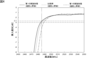
- FIG. 3 shows the attenuation frequency characteristics of the filter devices of the first embodiment and the comparative example of the present invention when the temperature is sufficiently increased, and the filter device of the first embodiment when the temperature is not increased. It is a figure which shows the attenuation amount frequency characteristic in a state.
- FIG. 4 is an enlarged view of FIG. 3, showing the vicinity of the frequency at which power is applied to the filter device.
- FIG. 5 is a schematic cross-sectional view showing part of a filter device according to a first modification of the first embodiment of the invention.
- FIG. 6 is a schematic cross-sectional view showing part of a filter device according to a second modification of the first embodiment of the invention.
- FIG. 7 is a schematic cross-sectional view showing part of a filter device according to a third modification of the first embodiment of the invention.
- FIG. 8 is a schematic cross-sectional view showing part of a filter device according to a fourth modification of the first embodiment of the invention.
- FIG. 9 is a schematic diagram of a filter device according to a second embodiment of the present invention.
- FIG. 1 is a schematic circuit diagram of the filter device according to the first embodiment of the present invention.
- the filter device 1 of this embodiment is a ladder filter.
- the filter device 1 has a first signal terminal 3A, a second signal terminal 3B, a plurality of series arm resonators, and a plurality of parallel arm resonators.
- the plurality of series arm resonators of the filter device 1 are a series arm resonator S1, a series arm resonator S2, a series arm resonator S3, a series arm resonator S4, and a series arm resonator S5.
- the plurality of parallel arm resonators are a parallel arm resonator P1, a parallel arm resonator P2, a parallel arm resonator P3 and a parallel arm resonator P4.
- all series arm resonators and all parallel arm resonators are elastic wave resonators.
- the first signal terminal 3A is an input terminal.
- the second signal terminal 3B is an antenna terminal. An antenna terminal is connected to the antenna.
- the first signal terminal 3A and the second signal terminal 3B may be configured as wiring, or may be configured as electrode pads.
- a series arm resonator S1, a series arm resonator S2, a series arm resonator S3, a series arm resonator S4, and a series arm resonator S5 are connected in series between the first signal terminal 3A and the second signal terminal 3B. It is connected.
- a parallel arm resonator P1 is connected between the connection point between the series arm resonators S1 and S2 and the ground potential.
- a parallel arm resonator P2 is connected between the connection point between the series arm resonators S2 and S3 and the ground potential.
- a parallel arm resonator P3 is connected between the connection point between the series arm resonators S3 and S4 and the ground potential.
- a parallel arm resonator P4 is connected between the connection point between the series arm resonators S4 and S5 and the ground potential.
- the circuit configuration of the filter device 1 is not limited to the above. At least one series arm resonator and at least one parallel arm resonator should be provided. However, it is preferable that a plurality of series arm resonators and a plurality of parallel arm resonators are provided. In this case, it is easy to improve the filter characteristics.
- the filter device 1 is a Band 7 transmission filter. More specifically, the pass band of the filter device 1 is 2500-2570 MHz. However, the pass band of the filter device 1 is not limited to the above. Furthermore, the filter device 1 may be a receive filter.
- the filter device 1 has multiple first wirings 6 and multiple second wirings 7 .
- a plurality of first wirings 6 respectively connect the series arm resonators and the parallel arm resonators. Furthermore, the first wiring 6 connects two series arm resonators. The first wiring 6 may connect the first signal terminal 3A or the second signal terminal 3B and the series arm resonator. The first wiring 6 should just connect the series arm resonator and the parallel arm resonator.
- each of the plurality of second wirings 7 connects the parallel arm resonator and the ground potential.
- the plurality of first wirings 6 are made of Al.
- the plurality of second wirings 7 are made of Mo.
- the materials of the plurality of first wirings 6 and the plurality of second wirings 7 are not limited to the above.
- the phrase "a certain member is made of a certain material" includes the case where a minute amount of impurity is contained to such an extent that the electrical characteristics of the filter device are not degraded.
- a specific configuration of the acoustic wave resonator in the first embodiment is shown below.
- FIG. 2 is a plan view showing the electrode configuration of the parallel arm resonator in the first embodiment. Note that the wiring connected to the parallel arm resonator P1 is omitted in FIG.
- the parallel arm resonator P1 has a piezoelectric substrate 2.
- the piezoelectric substrate 2 is a substrate consisting of only a piezoelectric layer.
- the piezoelectric layer is made of lithium tantalate.
- the material of the piezoelectric layer is not limited to the above, and lithium niobate, for example, can also be used.
- the piezoelectric substrate 2 may be a laminated substrate including piezoelectric layers.
- An IDT (Interdigital Transducer) electrode 4 as a functional electrode is provided on the piezoelectric substrate 2 .
- An AC voltage to the IDT electrodes 4 By applying an AC voltage to the IDT electrodes 4, elastic waves are excited.
- a pair of reflectors 5A and 5B are provided on both sides of the IDT electrode 4 on the piezoelectric substrate 2 in the elastic wave propagation direction.
- Each of the reflectors 5A and 5B has a plurality of electrode fingers. Both ends of a plurality of electrode fingers are short-circuited in each of the reflectors 5A and 5B.
- the IDT electrode 4 has a first busbar 8a and a second busbar 8b, and a plurality of first electrode fingers 9a and a plurality of second electrode fingers 9b.
- the first busbar 8a and the second busbar 8b face each other.
- One end of each of the plurality of first electrode fingers 9a is connected to the first bus bar 8a.
- One end of each of the plurality of second electrode fingers 9b is connected to the second bus bar 8b.
- the plurality of first electrode fingers 9a and the plurality of second electrode fingers 9b are interdigitated with each other.
- the overlapping region is the region where the adjacent first electrode fingers 9a and second electrode fingers 9b overlap each other. An acoustic wave is excited in the intersection region.
- the first electrode finger 9a and the second electrode finger 9b may be simply referred to as electrode fingers.
- the electrode finger extension direction In the following description, the first electrode finger 9a and the second electrode finger 9b may be simply referred to as electrode fingers.
- the electrode finger extension direction and the elastic wave propagation direction are orthogonal to each other.
- All acoustic wave resonators of the filter device 1 share the piezoelectric substrate 2 .
- Each acoustic wave resonator other than the parallel arm resonator P1 also has an IDT electrode and a reflector similarly to the parallel arm resonator P1.
- both the series arm resonators and the parallel arm resonators are surface acoustic wave resonators.
- the piezoelectric substrate 2 is made of lithium tantalate. Therefore, the temperature coefficient of frequency (TCF) of each surface acoustic wave resonator in the filter device 1 is a negative value.
- the plurality of first wirings 6 and the plurality of second wirings 7 shown in FIG. 1 are provided on the piezoelectric substrate 2 . Furthermore, at least one ground terminal is provided on the piezoelectric substrate 2 . Each second wiring 7 is connected to a ground terminal. The ground terminal is connected to ground potential.
- a feature of this embodiment is that the heat dissipation of all the second wirings 7 is lower than the heat dissipation of all the first wirings 6 .
- all the first wirings 6 are made of Al.
- All second wirings 7 are made of Mo.
- Al has a thermal conductivity of 236 W/m/K and Mo has a thermal conductivity of 147 W/m/K.
- the heat dissipation property of the second wiring 7 is lower than the heat dissipation property of the first wiring 6 .
- the heat dissipation of at least one second wiring 7 should be lower than the heat dissipation of all the first wirings 6 .
- the power durability can be improved without deteriorating the transmission characteristics. This will be explained below by comparing the present embodiment and a comparative example.
- the comparative example differs from the first embodiment in that both the first wiring and the second wiring are made of Al.
- the heat dissipation properties of the first wiring and the second wiring are the same.
- the attenuation frequency characteristics were compared between the first embodiment and the comparative example.
- FIG. 3 below shows attenuation frequency characteristics in a state where a sufficient amount of time has passed and the temperature has risen sufficiently after power is applied to the filter devices of the first embodiment and the comparative example.
- FIG. 3 also shows attenuation frequency characteristics in a state where the temperature does not rise immediately after power is applied to the filter device of the first embodiment.
- the attenuation frequency characteristics in a state where the temperature does not rise immediately after power is applied to the filter device are almost the same.
- Design parameters in the filter devices of the first embodiment and the comparative example are as shown in Table 1 below.
- the reference numerals indicating elastic wave resonators in Table 1 match the reference numerals indicating series arm resonators and parallel arm resonators in this specification.
- the dimension along the extending direction of the electrode fingers of the intersecting region is defined as the intersecting width.
- the wavelength of the IDT electrode is defined by the electrode finger pitch of the IDT electrode.
- the wavelength of the reflector is the wavelength defined by the electrode finger pitch of the reflector.
- the electrode finger pitch is the center-to-center distance between adjacent electrode fingers. The distance between the tip of the first electrode finger and the second bus bar or the distance between the tip of the second electrode finger and the first bus bar is defined as the inter-electrode gap length.
- FIG. 3 shows the attenuation frequency characteristics of the filter devices of the first embodiment and the comparative example when the temperature is sufficiently increased, and the attenuation of the filter device of the first embodiment when the temperature is not increased.
- FIG. 10 is a diagram showing a quantity-frequency characteristic
- FIG. 4 is an enlarged view of FIG. 3, showing the vicinity of the frequency at which power is applied to the filter device.
- the frequency for applying power to the filter device 1 may be referred to as power application frequency.
- the power application frequency is indicated by a chain double-dashed line.
- the attenuation frequency characteristic shifts to the low frequency side as a whole from the state in which the temperature does not rise to the state in which the temperature rises.
- the attenuation frequency characteristics are almost the same when the temperature does not rise. Therefore, even in the comparative example, it can be seen that the attenuation frequency characteristic is shifted to the low-frequency side as a whole as the temperature rises.
- the magnitude of the insertion loss in the comparative example is 3 dB.
- the magnitude of the insertion loss at the power application frequency is as small as 2.7 dB.
- the lower the insertion loss at the power application frequency the lower the amount of heat generated at the functional electrode. Therefore, in the first embodiment, the IDT electrode 4 as a functional electrode is less likely to be damaged, and power resistance can be improved. This is because, as shown in FIG. 4, in the first embodiment, the amount of frequency shift due to temperature rise is large on the low-pass side of the passband. Specifically, on the low-pass side of the passband, the amount of frequency shift due to temperature rise is 2.2 MHz larger in the first embodiment than in the comparative example.
- each parallel arm resonator propagates to each second wiring 7 . Then, the heat is radiated from each second wiring 7 to the outside. Alternatively, the heat is radiated to the outside through the second wirings 7, ground terminals, wirings to which the ground terminals are connected, and the like.
- the heat dissipation of each second wiring 7 in the first embodiment is low. Therefore, the heat dissipation of each parallel arm resonator is also low.
- the amount of change in resonance frequency in each parallel arm resonator increases as the temperature rises. Along with this, in the attenuation amount frequency characteristic of the filter device 1 as well, the amount of frequency shift on the low-pass side of the passband increases.
- the insertion loss is reduced at the power application frequency, and the power durability can be improved.
- the heat dissipation of the second wiring 7 is lowered, instead of adjusting the elastic wave resonator itself, which deteriorates the transmission characteristics, for example. Therefore, it is possible to improve the power durability without deteriorating the transmission characteristics.
- the heat dissipation of all the second wirings 7 is lower than the heat dissipation of all the first wirings 6 . Thereby, power durability can be improved more reliably.
- the materials of the first wiring 6 and the second wiring 7 are different. More specifically, the thermal conductivity of the material of the second wiring 7 is lower than the thermal conductivity of the material of the first wiring 6 . As a result, the heat dissipation of the second wiring 7 is lower than that of the first wiring 6 .
- the heat dissipation property of the second wiring 7 may be lower than the heat dissipation property of the first wiring 6 by a configuration other than the above. An example of this is shown below by a first modification and a second modification of the first embodiment. A first variant and a second variant are illustrated by the following schematic sectional views.
- each acoustic wave resonator is shown by a schematic diagram of a rectangle with two diagonal lines added.
- the series arm resonator S1 the parallel arm resonator P1
- the first wiring 6 and the second wiring 7 are schematically shown side by side.
- the arrangement of each elastic wave resonator and each wiring is not particularly limited.
- the piezoelectric substrate 2 is covered with a plurality of series arm resonators, a plurality of parallel arm resonators, a plurality of first wirings 6 and a plurality of second wirings 7.
- a dielectric film is provided. More specifically, the dielectric films include a first dielectric film 18A, a second dielectric film 18B, a third dielectric film 18C and a fourth dielectric film 18D.
- a first dielectric film 18A covers each first wiring 6 .
- a second dielectric film 18B covers each second wiring 7 .
- a third dielectric film 18C covers each elastic wave resonator.
- a fourth dielectric film 18 ⁇ /b>D covers the ground terminal 19 .
- the first dielectric film 18A, the second dielectric film 18B, the third dielectric film 18C, and the fourth dielectric film 18D are integrally provided.
- the first dielectric film 18A, the second dielectric film 18B, the third dielectric film 18C and the fourth dielectric film 18D may be provided separately.
- FIG. 5 the boundary between the first dielectric film 18A, the second dielectric film 18B, the third dielectric film 18C and the fourth dielectric film 18D, the second wiring 7 and the ground terminal 19 boundaries are indicated by dashed lines. The same applies to other schematic cross-sectional views.
- the thickness of the second dielectric film 18B is thicker than the thickness of the first dielectric film 18A.
- the heat dissipation property of the second wiring 7 is lower than the heat dissipation property of the first wiring 6 .
- the thicknesses of the third dielectric film 18C and the fourth dielectric film 18D are not particularly limited.
- the thickness of the third dielectric film 18C is the same as the thickness of the first dielectric film 18A.
- the thickness of the fourth dielectric film 18D is the same as the thickness of the second dielectric film 18B.
- the first dielectric film 18A, the second dielectric film 18B, the third dielectric film 18C and the fourth dielectric film 18D are silicon oxide films.
- the materials of the first dielectric film 18A, the second dielectric film 18B, the third dielectric film 18C and the fourth dielectric film 18D are not limited to silicon oxide, and may be silicon nitride or oxynitride. Silicon or the like can also be used.
- the first wiring 6 and the second wiring 7 may be made of the same material.
- the arithmetic mean roughness of the second wiring 7 is smaller than the arithmetic mean roughness of the first wiring 6.
- the heat dissipation of the second wiring 7 is lower than that of the first wiring 6 .
- the first wiring 6 and the second wiring 7 may be made of the same material.
- the arithmetic mean roughness in this specification conforms to the arithmetic mean roughness Ra in JIS B 0601:2001.
- the piezoelectric substrate 12A has a first portion 12c and a second portion 12d.
- the first portion 12c is a portion of the piezoelectric substrate 12A where the first wiring 6 is provided.
- the second portion 12d is a portion of the piezoelectric substrate 12A where the second wiring 7 is provided.
- the arithmetic mean roughness of the second portion 12d is smaller than the arithmetic mean roughness of the first portion 12c.
- the arithmetic mean roughness of the second wiring 7 is reduced by providing the second wiring 7 in a portion of the piezoelectric substrate 12A where the arithmetic mean roughness is small. In this case, the arithmetic mean roughness of the second wirings 7 can be easily made smaller than the arithmetic mean roughness of the first wirings 6 .
- the first wiring 6 and the second wiring 7 may be subjected to surface treatment such as blasting, and the surface treatment conditions may be different between the first wiring 6 and the second wiring 7. .
- the arithmetic mean roughness of the second wiring 7 may be smaller than the arithmetic mean roughness of the first wiring 6 .
- the arithmetic mean roughness in the piezoelectric substrate 12A may be the same in the first portion 12c and the second portion 12d.
- a first dielectric film 18A, a second dielectric film 18B, a third dielectric film 18C and a fourth dielectric film 18D are provided.
- the thickness of each dielectric film is the same.
- the second wiring 7 is made of an amorphous solid.
- amorphous solids the arrangement of atoms is random. Therefore, lattice vibration is difficult to propagate, and the mean free path of phonons is short.
- the thermal conductivity of amorphous solids is significantly lower than that of crystalline solids.
- the second wiring 7 of this modified example is made of an amorphous solid, the heat dissipation of the second wiring 7 can be further reduced. As a result, it is possible to further increase the amount of change in the resonance frequency of the parallel arm resonator that accompanies temperature rise. Therefore, the insertion loss can be more reliably reduced at the power application frequency, and the power durability can be more reliably increased.
- the first wiring 6 may be made of a crystalline solid.
- the first wiring 6 may be made of, for example, a single crystal or a polycrystal. More specifically, the first wiring 6 may be made of, for example, an epitaxially grown oriented film.
- an epitaxially grown oriented film refers to a polycrystalline film having a twin crystal structure.
- the piezoelectric substrate 2 in the first embodiment consists of only the piezoelectric layer.
- the piezoelectric substrate 2 may be a laminated substrate including piezoelectric layers.
- the piezoelectric substrate 12B includes a supporting substrate 13, a high acoustic velocity film 14 as a high acoustic velocity material layer, a low acoustic velocity film 15, and a piezoelectric and a body layer 16 .
- a high acoustic velocity film 14 is provided on the support substrate 13 .
- a low acoustic velocity film 15 is provided on the high acoustic velocity film 14 .
- a piezoelectric layer 16 is provided on the low-frequency film 15 .
- the heat dissipation of the second wiring 7 is lower than that of the first wiring 6, as in the first embodiment. As a result, the power durability can be improved without deteriorating the transmission characteristics.
- the low sound velocity film 15 is a relatively low sound velocity film. More specifically, the acoustic velocity of the bulk wave propagating through the low velocity film 15 is lower than the acoustic velocity of the bulk wave propagating through the piezoelectric layer 16 .
- the material of the low sound velocity film 15 for example, glass, silicon oxide, silicon oxynitride, lithium oxide, tantalum pentoxide, or a material mainly composed of a compound obtained by adding fluorine, carbon, or boron to silicon oxide may be used. can be done.
- the main component means a component that accounts for more than 50 wt %.
- the material of the main component may exist in a single crystal, polycrystal, or amorphous state, or in a state in which these are mixed.
- the high acoustic velocity material layer is a relatively high acoustic velocity layer.
- the high acoustic velocity material layer is the high acoustic velocity film 14 .
- the acoustic velocity of bulk waves propagating through the high acoustic velocity material layer is higher than the acoustic velocity of elastic waves propagating through the piezoelectric layer 16 .
- Materials for the high-sonic material layer include, for example, aluminum nitride, lithium tantalate, lithium niobate, piezoelectrics such as crystal, alumina, sapphire, magnesia, silicon nitride, silicon carbide, zirconia, cordierite, mullite, steatite, Ceramics such as forsterite, spinel, sialon, etc., aluminum oxide, silicon oxynitride, DLC (diamond-like carbon), dielectrics such as diamond, semiconductors such as silicon, or materials containing the above materials as main components can be used.
- the above spinel includes an aluminum compound containing one or more elements selected from Mg, Fe, Zn, Mn, etc. and oxygen. Examples of the spinels include MgAl2O4 , FeAl2O4 , ZnAl2O4 , and MnAl2O4 .
- Materials for the support substrate 13 include, for example, aluminum oxide, lithium tantalate, lithium niobate, piezoelectric materials such as crystal, alumina, sapphire, magnesia, silicon nitride, aluminum nitride, silicon carbide, zirconia, cordierite, mullite, and steer.
- Various ceramics such as tight and forsterite, dielectrics such as diamond and glass, semiconductors such as silicon and gallium nitride, and resins can be used.
- a high acoustic velocity film 14 as a high acoustic velocity material layer, a low acoustic velocity film 15 and a piezoelectric layer 16 are laminated in this order on the piezoelectric substrate 12B. Thereby, the elastic wave energy can be effectively confined to the piezoelectric layer 16 side.
- the laminated structure of the piezoelectric substrate is not limited to the above.
- the piezoelectric substrate may be a laminated substrate of a supporting substrate, a high acoustic velocity film and a piezoelectric layer.
- the high acoustic velocity material layer may be a high acoustic velocity support substrate.
- the piezoelectric substrate may be a laminated substrate of a high acoustic velocity supporting substrate, a low acoustic velocity film and a piezoelectric layer, or may be a laminated substrate of a high acoustic velocity supporting substrate and a piezoelectric layer.
- the energy of elastic waves can be effectively confined in the piezoelectric layer.
- FIG. 9 is a schematic diagram of a filter device according to the second embodiment.
- the filter device 20 of this embodiment is a composite filter device. More specifically, filter device 20 is a multiplexer.
- filter devices other than composite filter devices such as band-pass filters, may be referred to as filters.
- the filter device 20 has a common connection terminal 22, a first filter 21A, a second filter 21B, a third filter 21C, and at least one other filter.
- a plurality of filters are commonly connected to a common connection terminal 22 .
- the common connection terminal 22 may be configured as wiring, or may be configured as an electrode pad. Note that the number of filters in the filter device 20 is not particularly limited. If filter device 20 is a multiplexer, filter device 20 need only have three or more filters.
- the first filter 21A, the second filter 21B and the third filter 21C are band-pass filters.
- the first filter 21A is a transmission filter having a configuration similar to that of the first embodiment.
- the first filter 21A may be any filter according to the present invention.
- the filter device 20 need only have at least one filter according to the invention.
- the filter device 20 has a first filter 21A configured similarly to the first embodiment. Therefore, it is possible to improve the power durability without deteriorating the transmission characteristics.
- the filter device 20 may be a duplexer or the like having two filters. Also in this case, the filter device 20 only needs to have at least one filter according to the invention.
- Reference Signs List 1 Filter device 2 Piezoelectric substrates 3A, 3B First and second signal terminals 4 IDT electrodes 5A and 5B Reflectors 6 and 7 First and second wirings 8a and 8b First and second 2 bus bars 9a, 9b... first and second electrode fingers 12A, 12B... piezoelectric substrates 12c, 12d... first and second portions 13... support substrate 14... high acoustic velocity film 15... low acoustic velocity film 16... piezoelectric Body layers 18A to 18D First to fourth dielectric films 19 Ground terminal 20 Filter devices 21A to 21C First to third filters 22 Common connection terminals P1 to P4 Parallel arm resonators S1 to S5 ... series arm resonator
Landscapes
- Physics & Mathematics (AREA)
- Acoustics & Sound (AREA)
- Surface Acoustic Wave Elements And Circuit Networks Thereof (AREA)
Abstract
伝送特性の劣化を招かずして、耐電力性を高めることができる、フィルタ装置を提供する。 本発明のフィルタ装置1は、圧電性基板と、圧電性基板上において構成されている直列腕共振子S1~S5と、圧電性基板上において構成されている並列腕共振子P1~P4と、圧電性基板上に設けられており、直列腕共振子及び並列腕共振子を接続している第1の配線6と、圧電性基板上に設けられており、並列腕共振子とグラウンド電位とを接続している第2の配線7とを備える。少なくとも1つの第2の配線7の放熱性が全ての第1の配線6の放熱性よりも低い。
Description
本発明は、フィルタ装置に関する。
従来、弾性波共振子を有するフィルタ装置は携帯電話機などに広く用いられている。下記の特許文献1には、弾性波共振子を用いたフィルタ装置としての、弾性表面波デバイスの一例が開示されている。この弾性表面波デバイスにおいては、直列共振器及び並列共振器はそれぞれ、櫛形電極を有する。直列共振器及び並列共振器は弾性波共振子である。直列共振器及び並列共振器の櫛形電極上には、保護膜が設けられている。直列共振器の櫛形電極上に設けられた保護膜の厚みは70Åである。並列共振器の櫛形電極上に設けられた保護膜の厚みは2000Åである。このように、保護膜の厚みを異ならせることにより、周波数特性の調整が図られている。なお、保護膜にはSiO2が用いられている。
特許文献1に記載された弾性表面波デバイスにおいては、例えば、櫛形電極のピッチを調整することによって耐電力性の改善を図る場合、保護膜の厚みも調整する必要がある。保護膜の厚みを最適値から変化させると、不要波が生じるおそれがある。そのため、伝送特性が劣化するおそれがある。
本発明の目的は、伝送特性の劣化を招かずして、耐電力性を高めることができる、フィルタ装置を提供することにある。
本発明に係るフィルタ装置は、圧電性基板と、前記圧電性基板上において構成されている直列腕共振子と、前記圧電性基板上において構成されている並列腕共振子と、前記圧電性基板上に設けられており、前記直列腕共振子及び前記並列腕共振子を接続している第1の配線と、前記圧電性基板上に設けられており、前記並列腕共振子とグラウンド電位とを接続している第2の配線とを備え、少なくとも1つの前記第2の配線の放熱性が全ての前記第1の配線の放熱性よりも低い。
本発明に係るフィルタ装置によれば、伝送特性の劣化を招かずして、耐電力性を高めることができる。
以下、図面を参照しつつ、本発明の具体的な実施形態を説明することにより、本発明を明らかにする。
なお、本明細書に記載の各実施形態は、例示的なものであり、異なる実施形態間において、構成の部分的な置換または組み合わせが可能であることを指摘しておく。
図1は、本発明の第1の実施形態に係るフィルタ装置の模式的回路図である。
本実施形態のフィルタ装置1はラダー型フィルタである。フィルタ装置1は、第1の信号端子3Aと、第2の信号端子3Bと、複数の直列腕共振子と、複数の並列腕共振子とを有する。より具体的には、フィルタ装置1の複数の直列腕共振子は、直列腕共振子S1、直列腕共振子S2、直列腕共振子S3、直列腕共振子S4及び直列腕共振子S5である。複数の並列腕共振子は、並列腕共振子P1、並列腕共振子P2、並列腕共振子P3及び並列腕共振子P4である。フィルタ装置1においては、全ての直列腕共振子及び全ての並列腕共振子は弾性波共振子である。
本実施形態においては、第1の信号端子3Aは入力端子である。第2の信号端子3Bはアンテナ端子である。アンテナ端子はアンテナに接続される。第1の信号端子3A及び第2の信号端子3Bは、配線として構成されていてもよく、あるいは、電極パッドとして構成されていてもよい。
第1の信号端子3A及び第2の信号端子3Bの間に、直列腕共振子S1、直列腕共振子S2、直列腕共振子S3、直列腕共振子S4及び直列腕共振子S5が互いに直列に接続されている。直列腕共振子S1及び直列腕共振子S2の間の接続点とグラウンド電位との間に、並列腕共振子P1が接続されている。直列腕共振子S2及び直列腕共振子S3の間の接続点とグラウンド電位との間に、並列腕共振子P2が接続されている。直列腕共振子S3及び直列腕共振子S4の間の接続点とグラウンド電位との間に、並列腕共振子P3が接続されている。直列腕共振子S4及び直列腕共振子S5の間の接続点とグラウンド電位との間に、並列腕共振子P4が接続されている。なお、フィルタ装置1の回路構成は上記に限定されない。少なくとも1個の直列腕共振子及び少なくとも1個の並列腕共振子が設けられていればよい。もっとも、複数の直列腕共振子及び複数の並列腕共振子が設けられていることが好ましい。この場合には、フィルタ特性を良好とし易い。
フィルタ装置1はBand7の送信フィルタである。より具体的には、フィルタ装置1の通過帯域は、2500~2570MHzである。もっとも、フィルタ装置1の通過帯域は上記に限定されない。さらに、フィルタ装置1は受信フィルタであってもよい。
図1に模式的に示すように、フィルタ装置1は、複数の第1の配線6と、複数の第2の配線7とを有する。複数の第1の配線6はそれぞれ、直列腕共振子及び並列腕共振子を接続している。さらに、第1の配線6は2個の直列腕共振子同士を接続している。なお、第1の配線6は、第1の信号端子3Aまたは第2の信号端子3Bと、直列腕共振子とを接続していてもよい。第1の配線6は、直列腕共振子及び並列腕共振子を接続していればよい。他方、複数の第2の配線7はそれぞれ、並列腕共振子及びグラウンド電位を接続している。
複数の第1の配線6はAlからなる。複数の第2の配線7はMoからなる。もっとも、複数の第1の配線6及び複数の第2の配線7の材料は上記に限定されない。なお、本明細書において、ある部材がある材料からなるとは、フィルタ装置の電気的特性が劣化しない程度の微量な不純物が含まれる場合を含む。
以下において、第1の実施形態における弾性波共振子の具体的な構成を示す。
図2は、第1の実施形態における並列腕共振子の電極構成を示す平面図である。なお、図2においては、並列腕共振子P1に接続された配線は省略している。
並列腕共振子P1は圧電性基板2を有する。本実施形態においては、圧電性基板2は圧電体層のみからなる基板である。圧電体層はタンタル酸リチウムからなる。もっとも、圧電体層の材料は上記に限定されず、例えば、ニオブ酸リチウムなどを用いることもできる。なお、圧電性基板2は、圧電体層を含む積層基板であってもよい。
圧電性基板2上に、機能電極としてのIDT(Interdigital Transducer)電極4が設けられている。IDT電極4に交流電圧を印加することにより、弾性波が励振される。圧電性基板2上における、IDT電極4の弾性波伝搬方向両側に、1対の反射器5A及び反射器5Bが設けられている。なお、反射器5A及び反射器5Bはそれぞれ、複数の電極指を有する。反射器5A及び反射器5Bのそれぞれにおいて、複数の電極指の両端が短絡されている。
IDT電極4は、第1のバスバー8a及び第2のバスバー8bと、複数の第1の電極指9a及び複数の第2の電極指9bとを有する。第1のバスバー8a及び第2のバスバー8bは互いに対向している。第1のバスバー8aに、複数の第1の電極指9aの一端がそれぞれ接続されている。第2のバスバー8bに、複数の第2の電極指9bの一端がそれぞれ接続されている。複数の第1の電極指9a及び複数の第2の電極指9bは互いに間挿し合っている。弾性波伝搬方向から見たときに、隣り合う第1の電極指9a及び第2の電極指9bが重なり合っている領域が交叉領域である。交叉領域において弾性波が励振される。なお、以下においては、第1の電極指9a及び第2の電極指9bを単に電極指と記載することがある。複数の電極指が延びる方向を電極指延伸方向としたときに、本実施形態では、電極指延伸方向及び弾性波伝搬方向は互いに直交している。
フィルタ装置1の全ての弾性波共振子は、圧電性基板2を共有している。並列腕共振子P1以外の各弾性波共振子もそれぞれ、並列腕共振子P1と同様に、IDT電極及び反射器を有する。本実施形態においては、複数の直列腕共振子及び複数の並列腕共振子はいずれも、弾性表面波共振子である。上記のように、本実施形態においては、圧電性基板2はタンタル酸リチウムからなる。そのため、フィルタ装置1における各弾性表面波共振子の周波数温度係数(TCF)は負の値である。
なお、図1に示す複数の第1の配線6及び複数の第2の配線7は、圧電性基板2上に設けられている。さらに、圧電性基板2上には、少なくとも1つのグラウンド端子が設けられている。各第2の配線7はグラウンド端子に接続されている。グラウンド端子はグラウンド電位に接続される。
本実施形態の特徴は、全ての第2の配線7の放熱性が全ての第1の配線6の放熱性よりも低いことにある。より具体的には、フィルタ装置1においては、全ての第1の配線6はAlからなる。全ての第2の配線7はMoからなる。Alの熱伝導率は236W/m/Kであり、Moの熱伝導率は147W/m/Kである。これにより、第2の配線7の放熱性が第1の配線6の放熱性よりも低い。もっとも、少なくとも1つの第2の配線7の放熱性が全ての第1の配線6の放熱性よりも低ければよい。それによって、伝送特性の劣化を招かずして、耐電力性を高めることができる。これを、本実施形態と比較例とを比較することにより、以下において説明する。
比較例は、第1の配線及び第2の配線の双方がAlからなる点において、第1の実施形態と異なる。比較例においては、第1の配線及び第2の配線の放熱性は同じである。第1の実施形態及び比較例において、減衰量周波数特性を比較した。なお、下記の図3においては、第1の実施形態及び比較例のフィルタ装置に電力を印加してから、十分に時間が経過し、温度が十分に上昇した状態における減衰量周波数特性を示す。加えて、図3においては、第1の実施形態のフィルタ装置に電力を印加した直後の、温度が上昇していない状態における減衰量周波数特性も示す。なお、第1の実施形態及び比較例においては、フィルタ装置に電力を印加した直後の、温度が上昇していない状態における減衰量周波数特性はほぼ変わらない。第1の実施形態及び比較例のフィルタ装置における設計パラメータは、下記の表1の通りである。表1における弾性波共振子を示す符号は、本明細書における直列腕共振子及び並列腕共振子を示す符号と一致する。
以下においては、交叉領域の電極指延伸方向に沿う寸法を交叉幅とする。さらに、IDT電極の波長は、IDT電極の電極指ピッチにより規定される波長である。反射器の波長は、反射器の電極指ピッチにより規定される波長である。なお、電極指ピッチとは、隣り合う電極指同士の中心間距離である。第1の電極指の先端及び第2のバスバーの間の距離、または第2の電極指の先端及び第1のバスバーの間の距離を電極間ギャップ長とする。

図3は、第1の実施形態及び比較例のフィルタ装置の、温度が十分に上昇した状態における減衰量周波数特性と、第1の実施形態のフィルタ装置の、温度が上昇していない状態における減衰量周波数特性とを示す図である。図4は、図3の拡大図であって、フィルタ装置に電力を印加する周波数付近を示す図である。以下においては、フィルタ装置1に電力を印加する周波数を、電力印加周波数と記載することがある。図4では、電力印加周波数を二点鎖線により示す。
図3に示すように、第1の実施形態においては、温度が上昇していない状態から温度が上昇した状態にかけて、減衰量周波数特性が全体的に低域側に移動している。なお、上述したように、第1の実施形態及び比較例においては、温度が上昇していない状態における減衰量周波数特性はほぼ変わらない。よって、比較例においても、温度の上昇により、減衰量周波数特性が全体的に低域側に移動していることがわかる。
図4中の二点鎖線により示す電力印加周波数においては、比較例における挿入損失の大きさは3dBである。これに対して、第1の実施形態においては、電力印加周波数における挿入損失の大きさは2.7dBと小さくなっている。電力印加周波数において挿入損失が小さくなると、機能電極において生じる熱量も低くなる。よって、第1の実施形態においては、機能電極としてのIDT電極4が破損し難く、耐電力性を高めることができる。これは、図4に示すように、第1の実施形態では、通過帯域の低域側において、温度の上昇による周波数の移動量が大きいことによる。具体的には、通過帯域の低域側において、第1の実施形態では比較例よりも、温度の上昇による周波数の移動量が2.2MHz大きい。
第1の実施形態においては、各並列腕共振子において生じた熱は、各第2の配線7に伝搬する。そして、各第2の配線7から外部に放熱される。あるいは、各第2の配線7、グラウンド端子、並びにグラウンド端子が接続される配線などを経て外部に放熱される。もっとも、第1の実施形態における各第2の配線7の放熱性は低い。そのため、各並列腕共振子の放熱性も低い。それによって、温度の上昇に伴う、各並列腕共振子における共振周波数の変化量が大きくなる。これに伴い、フィルタ装置1の減衰量周波数特性においても、通過帯域の低域側における周波数の移動量が大きくなる。よって、図4に示すように、電力印加周波数において挿入損失が小さくなり、耐電力性を高めることができる。このように、第1の実施形態においては、例えば伝送特性が劣化するような、弾性波共振子自体の調整を行うのではなく、第2の配線7の放熱性を低くしている。従って、伝送特性の劣化を招かずして、耐電力性を高めることができる。
なお、全ての第2の配線7の放熱性が全ての第1の配線6の放熱性よりも低いことが好ましい。それによって、耐電力性をより確実に高めることができる。
第1の実施形態においては、第1の配線6及び第2の配線7の材料を異ならせている。より具体的には、第2の配線7の材料の熱伝導率が第1の配線6の材料の熱伝導率よりも低い。それによって、第2の配線7の放熱性が第1の配線6の放熱性よりも低い。もっとも、上記以外の構成により、第2の配線7の放熱性が第1の配線6の放熱性よりも低くなっていてもよい。この例を、以下において、第1の実施形態の第1の変形例及び第2の変形例により示す。第1の変形例及び第2の変形例は、以下の各略図的断面図により示す。各略図的断面図においては、各弾性波共振子を、矩形に2本の対角線を加えた略図により示す。各略図的断面図においては、直列腕共振子S1、並列腕共振子P1、第1の配線6及び第2の配線7を模式的に並べて示す。なお、各弾性波共振子及び各配線の配置は特に限定されるものではない。
図5に示す第1の変形例においては、圧電性基板2上に、複数の直列腕共振子、複数の並列腕共振子、複数の第1の配線6及び複数の第2の配線7を覆うように、誘電体膜が設けられている。より具体的には、誘電体膜は、第1の誘電体膜18A、第2の誘電体膜18B、第3の誘電体膜18C及び第4の誘電体膜18Dを含む。第1の誘電体膜18Aは各第1の配線6を覆っている。第2の誘電体膜18Bは各第2の配線7を覆っている。第3の誘電体膜18Cは各弾性波共振子を覆っている。第4の誘電体膜18Dはグラウンド端子19を覆っている。本変形例においては、第1の誘電体膜18A、第2の誘電体膜18B、第3の誘電体膜18C及び第4の誘電体膜18Dは一体として設けられている。もっとも、例えば、第1の誘電体膜18A、第2の誘電体膜18B、第3の誘電体膜18C及び第4の誘電体膜18Dは別体として設けられていてもよい。なお、図5においては、第1の誘電体膜18A、第2の誘電体膜18B、第3の誘電体膜18C及び第4の誘電体膜18Dの境界、並びに第2の配線7及びグラウンド端子19の境界を破線により示す。他の略図的断面図においても同様である。
本変形例においては、第2の誘電体膜18Bの厚みが、第1の誘電体膜18Aの厚みよりも厚い。これにより、第2の配線7の放熱性が第1の配線6の放熱性よりも低い。
他方、第3の誘電体膜18C及び第4の誘電体膜18Dの厚みは特に限定されない。本変形例では、第3の誘電体膜18Cの厚みは第1の誘電体膜18Aの厚みと同じである。第4の誘電体膜18Dの厚みは第2の誘電体膜18Bの厚みと同じである。
第1の誘電体膜18A、第2の誘電体膜18B、第3の誘電体膜18C及び第4の誘電体膜18Dは酸化ケイ素膜である。なお、第1の誘電体膜18A、第2の誘電体膜18B、第3の誘電体膜18C及び第4の誘電体膜18Dの材料は酸化ケイ素に限定されず、例えば、窒化ケイ素または酸窒化ケイ素などを用いることもできる。本変形例では、第1の配線6及び第2の配線7は同じ材料からなっていてもよい。
図6に示す第2の変形例においては、第2の配線7の算術平均粗さが、第1の配線6の算術平均粗さよりも小さい。それによって、第2の配線7の放熱性が第1の配線6の放熱性よりも低い。本変形例では、第1の配線6及び第2の配線7は同じ材料からなっていてもよい。なお、本明細書における算術平均粗さは、JIS B 0601:2001における算術平均粗さRaに準拠する。
本変形例では、圧電性基板12Aは第1の部分12c及び第2の部分12dを有する。第1の部分12cは、圧電性基板12Aにおける第1の配線6が設けられている部分である。第2の部分12dは、圧電性基板12Aにおける第2の配線7が設けられている部分である。第2の部分12dの算術平均粗さは、第1の部分12cの算術平均粗さよりも小さい。圧電性基板12Aにおける算術平均粗さが小さい部分に、第2の配線7を設けることにより、第2の配線7の算術平均粗さを小さくしている。この場合には、第2の配線7の算術平均粗さを第1の配線6の算術平均粗さよりも、容易に小さくすることができる。
もっとも、第1の配線6及び第2の配線7に、例えばブラスト処理などの表面処理を行い、かつ第1の配線6及び第2の配線7において、表面処理の条件を互いに異ならせてもよい。これにより、第2の配線7の算術平均粗さを第1の配線6の算術平均粗さよりも小さくしてもよい。このような場合には、圧電性基板12Aにおける算術平均粗さは、第1の部分12c及び第2の部分12dにおいて同じであってもよい。
本変形例においても、第1の誘電体膜18A、第2の誘電体膜18B、第3の誘電体膜18C及び第4の誘電体膜18Dが設けられている。本変形例では、上記各誘電体膜の厚みは同じである。
さらに、図7に示す第1の実施形態の第3の変形例においては、第2の配線7が非晶質固体からなる。非晶質固体においては、原子の配列がランダムである。そのため、格子振動が伝搬し難く、フォノンの平均自由行程が短い。よって、非晶質固体の熱伝導率は、結晶質固体の熱伝導率よりも大幅に低い。本変形例の第2の配線7は非晶質固体からなるため、第2の配線7の放熱性をより一層低くすることができる。これにより、温度の上昇に伴う並列腕共振子の共振周波数の変化量を、より一層大きくすることができる。従って、電力印加周波数において挿入損失をより確実に小さくすることができ、耐電力性をより確実に高めることができる。
他方、第1の配線6は結晶質固体からなっていてもよい。具体的には、第1の配線6は、例えば、単結晶体または多結晶体からなっていてもよい。より具体的には、第1の配線6は、例えば、エピタキシャル成長した配向膜からなっていてもよい。本明細書においてエピタキシャル成長した配向膜とは、双晶構造を有する多結晶膜をいう。第1の配線6が結晶質固体からなる場合には、第2の配線7の放熱性を第1の配線6の放熱性よりも、より確実に低くすることができる。この場合、第1の配線6及び第2の配線7において、材料の組成が同じであってもよい。
上記のように第1の実施形態における圧電性基板2は、圧電体層のみからなる。もっとも、圧電性基板2は、圧電体層を含む積層基板であってもよい。例えば、図8に示す第1の実施形態の第4の変形例においては、圧電性基板12Bは、支持基板13と、高音速材料層としての高音速膜14と、低音速膜15と、圧電体層16とを有する。支持基板13上に高音速膜14が設けられている。高音速膜14上に低音速膜15が設けられている。低音速膜15上に圧電体層16が設けられている。本変形例においても、第1の実施形態と同様に、第2の配線7の放熱性は第1の配線6の放熱性よりも低い。それによって、伝送特性の劣化を招かずして、耐電力性を高めることができる。
なお、低音速膜15は相対的に低音速な膜である。より具体的には、低音速膜15を伝搬するバルク波の音速は、圧電体層16を伝搬するバルク波の音速よりも低い。低音速膜15の材料としては、例えば、ガラス、酸化ケイ素、酸窒化ケイ素、酸化リチウム、五酸化タンタル、または、酸化ケイ素にフッ素、炭素やホウ素を加えた化合物を主成分とする材料を用いることができる。なお、本明細書において主成分とは、占める割合が50wt%を超える成分をいう。上記主成分の材料は、単結晶、多結晶、及びアモルファスのうちいずれかの状態、もしくは、これらが混在した状態で存在していてもよい。
高音速材料層は相対的に高音速な層である。本変形例では、高音速材料層は高音速膜14である。高音速材料層を伝搬するバルク波の音速は、圧電体層16を伝搬する弾性波の音速よりも高い。高音速材料層の材料としては、例えば、窒化アルミニウム、タンタル酸リチウム、ニオブ酸リチウム、水晶などの圧電体、アルミナ、サファイア、マグネシア、窒化ケイ素、炭化ケイ素、ジルコニア、コージライト、ムライト、ステアタイト、フォルステライト、スピネル、サイアロンなどのセラミック、酸化アルミニウム、酸窒化ケイ素、DLC(ダイヤモンドライクカーボン)、ダイヤモンドなどの誘電体、もしくはシリコンなどの半導体、または上記材料を主成分とする材料を用いることができる。なお、上記スピネルには、Mg、Fe、Zn、Mnなどから選ばれる1以上の元素と酸素とを含有するアルミニウム化合物が含まれる。上記スピネルの例としては、MgAl2O4、FeAl2O4、ZnAl2O4、MnAl2O4を挙げることができる。
支持基板13の材料としては、例えば、酸化アルミニウム、タンタル酸リチウム、ニオブ酸リチウム、水晶などの圧電体、アルミナ、サファイア、マグネシア、窒化ケイ素、窒化アルミニウム、炭化ケイ素、ジルコニア、コージライト、ムライト、ステアタイト、フォルステライトなどの各種セラミック、ダイヤモンド、ガラスなどの誘電体、シリコン、窒化ガリウムなどの半導体または樹脂などを用いることができる。
本変形例においては、圧電性基板12Bにおいて、高音速材料層としての高音速膜14、低音速膜15及び圧電体層16がこの順序において積層されている。それによって、弾性波のエネルギーを圧電体層16側に効果的に閉じ込めることができる。
なお、圧電性基板の積層構造は上記に限定されない。例えば、圧電性基板は、支持基板、高音速膜及び圧電体層の積層基板であってもよい。さらに、高音速材料層は、高音速支持基板であってもよい。この場合には、圧電性基板は、高音速支持基板、低音速膜及び圧電体層の積層基板であってもよく、あるいは、高音速支持基板及び圧電体層の積層基板であってもよい。これらの場合においても、弾性波のエネルギーを圧電体層側に効果的に閉じ込めることができる。さらに、第4の変形例と同様に、伝送特性の劣化を招かずして、耐電力性を高めることができる。
図9は、第2の実施形態に係るフィルタ装置の模式図である。
本実施形態のフィルタ装置20は複合フィルタ装置である。より具体的には、フィルタ装置20はマルチプレクサである。以下においては、例えば帯域通過型フィルタなどの、複合フィルタ装置以外のフィルタ装置をフィルタと記載することがある。
フィルタ装置20は、共通接続端子22と、第1のフィルタ21Aと、第2のフィルタ21Bと、第3のフィルタ21Cと、他の少なくとも1個のフィルタとを有する。複数のフィルタは共通接続端子22に共通接続されている。共通接続端子22は、配線として構成されていてもよく、あるいは、電極パッドとして構成されていてもよい。なお、フィルタ装置20におけるフィルタの個数は特に限定されない。フィルタ装置20がマルチプレクサである場合、フィルタ装置20は3個以上のフィルタを有していればよい。
本実施形態においては、第1のフィルタ21A、第2のフィルタ21B及び第3のフィルタ21Cは帯域通過型フィルタである。第1のフィルタ21Aは、第1の実施形態と同様の構成を有する送信フィルタである。もっとも、第1のフィルタ21Aは、本発明に係るフィルタであればよい。フィルタ装置20は、少なくとも1個の本発明に係るフィルタを有していればよい。
フィルタ装置20は、第1の実施形態と同様に構成された第1のフィルタ21Aを有する。よって、伝送特性の劣化を招かずして、耐電力性を高めることができる。
なお、フィルタ装置20は、2個のフィルタを有するデュプレクサなどであってもよい。この場合においても、フィルタ装置20は、少なくとも1個の本発明に係るフィルタを有していればよい。
1…フィルタ装置
2…圧電性基板
3A,3B…第1,第2の信号端子
4…IDT電極
5A,5B…反射器
6,7…第1,第2の配線
8a,8b…第1,第2のバスバー
9a,9b…第1,第2の電極指
12A,12B…圧電性基板
12c,12d…第1,第2の部分
13…支持基板
14…高音速膜
15…低音速膜
16…圧電体層
18A~18D…第1~第4の誘電体膜
19…グラウンド端子
20…フィルタ装置
21A~21C…第1~第3のフィルタ
22…共通接続端子
P1~P4…並列腕共振子
S1~S5…直列腕共振子
2…圧電性基板
3A,3B…第1,第2の信号端子
4…IDT電極
5A,5B…反射器
6,7…第1,第2の配線
8a,8b…第1,第2のバスバー
9a,9b…第1,第2の電極指
12A,12B…圧電性基板
12c,12d…第1,第2の部分
13…支持基板
14…高音速膜
15…低音速膜
16…圧電体層
18A~18D…第1~第4の誘電体膜
19…グラウンド端子
20…フィルタ装置
21A~21C…第1~第3のフィルタ
22…共通接続端子
P1~P4…並列腕共振子
S1~S5…直列腕共振子
Claims (7)
- 圧電性基板と、
前記圧電性基板上において構成されている直列腕共振子と、
前記圧電性基板上において構成されている並列腕共振子と、
前記圧電性基板上に設けられており、前記直列腕共振子及び前記並列腕共振子を接続している第1の配線と、
前記圧電性基板上に設けられており、前記並列腕共振子とグラウンド電位とを接続している第2の配線と、
を備え、
少なくとも1つの前記第2の配線の放熱性が全ての前記第1の配線の放熱性よりも低い、フィルタ装置。 - 全ての前記第2の配線の放熱性が全ての前記第1の配線の放熱性よりも低い、請求項1に記載のフィルタ装置。
- 前記圧電性基板上に、前記第1の配線を覆うように設けられている第1の誘電体膜、及び前記圧電性基板上に、前記第2の配線を覆うように設けられている第2の誘電体膜をさらに備え、
前記第2の誘電体膜の厚みが、前記第1の誘電体膜の厚みよりも厚い、請求項1または2に記載のフィルタ装置。 - 前記第1の誘電体膜及び前記第2の誘電体膜が酸化ケイ素膜である、請求項3に記載のフィルタ装置。
- 前記第2の配線の熱伝導率が、前記第1の配線の熱伝導率よりも低い、請求項1~4のいずれか1項に記載のフィルタ装置。
- 前記第2の配線の算術平均粗さが、前記第1の配線の算術平均粗さよりも小さい、請求項1~5のいずれか1項に記載のフィルタ装置。
- 前記第2の配線が非晶質固体からなる、請求項1~6のいずれか1項に記載のフィルタ装置。
Applications Claiming Priority (2)
| Application Number | Priority Date | Filing Date | Title |
|---|---|---|---|
| JP2021-170416 | 2021-10-18 | ||
| JP2021170416 | 2021-10-18 |
Publications (1)
| Publication Number | Publication Date |
|---|---|
| WO2023068128A1 true WO2023068128A1 (ja) | 2023-04-27 |
Family
ID=86058233
Family Applications (1)
| Application Number | Title | Priority Date | Filing Date |
|---|---|---|---|
| PCT/JP2022/038012 WO2023068128A1 (ja) | 2021-10-18 | 2022-10-12 | フィルタ装置 |
Country Status (1)
| Country | Link |
|---|---|
| WO (1) | WO2023068128A1 (ja) |
Citations (5)
| Publication number | Priority date | Publication date | Assignee | Title |
|---|---|---|---|---|
| JP2004282707A (ja) * | 2003-02-24 | 2004-10-07 | Murata Mfg Co Ltd | 弾性表面波フィルタ、通信機 |
| JP2007068231A (ja) * | 2006-11-30 | 2007-03-15 | Oki Electric Ind Co Ltd | 弾性表面波フィルタ及び弾性表面波フィルタパッケージ |
| JP2007074459A (ja) * | 2005-09-08 | 2007-03-22 | Hitachi Media Electoronics Co Ltd | 共振器型フィルタ |
| JP2020170983A (ja) * | 2019-04-05 | 2020-10-15 | 三安ジャパンテクノロジー株式会社 | 表面弾性波デバイス及びその製造方法 |
| JP2020198552A (ja) * | 2019-06-03 | 2020-12-10 | 太陽誘電株式会社 | 弾性波デバイス、フィルタ、及びマルチプレクサ |
-
2022
- 2022-10-12 WO PCT/JP2022/038012 patent/WO2023068128A1/ja unknown
Patent Citations (5)
| Publication number | Priority date | Publication date | Assignee | Title |
|---|---|---|---|---|
| JP2004282707A (ja) * | 2003-02-24 | 2004-10-07 | Murata Mfg Co Ltd | 弾性表面波フィルタ、通信機 |
| JP2007074459A (ja) * | 2005-09-08 | 2007-03-22 | Hitachi Media Electoronics Co Ltd | 共振器型フィルタ |
| JP2007068231A (ja) * | 2006-11-30 | 2007-03-15 | Oki Electric Ind Co Ltd | 弾性表面波フィルタ及び弾性表面波フィルタパッケージ |
| JP2020170983A (ja) * | 2019-04-05 | 2020-10-15 | 三安ジャパンテクノロジー株式会社 | 表面弾性波デバイス及びその製造方法 |
| JP2020198552A (ja) * | 2019-06-03 | 2020-12-10 | 太陽誘電株式会社 | 弾性波デバイス、フィルタ、及びマルチプレクサ |
Similar Documents
| Publication | Publication Date | Title |
|---|---|---|
| US10171061B2 (en) | Elastic wave device | |
| US11444601B2 (en) | Acoustic wave device | |
| US20220224311A1 (en) | Acoustic wave device | |
| US20220182037A1 (en) | Acoustic wave device | |
| US20230336143A1 (en) | Acoustic wave device | |
| US11996828B2 (en) | Filter device | |
| US20240154595A1 (en) | Acoustic wave device | |
| US20230327634A1 (en) | Acoustic wave device | |
| WO2023068128A1 (ja) | フィルタ装置 | |
| US20220416764A1 (en) | Acoustic wave device and composite filter device | |
| WO2023068129A1 (ja) | フィルタ装置 | |
| US20220263493A1 (en) | Acoustic wave device | |
| WO2021024762A1 (ja) | 弾性波フィルタ装置 | |
| WO2024080205A1 (ja) | フィルタ装置 | |
| WO2024070893A1 (ja) | 弾性波装置 | |
| US20240014801A1 (en) | Acoustic wave device | |
| US20240243728A1 (en) | Filter device | |
| WO2022019169A1 (ja) | ラダー型フィルタ | |
| WO2022102621A1 (ja) | 弾性波装置 | |
| WO2023002909A1 (ja) | 複合フィルタ装置 | |
| WO2024143006A1 (ja) | 弾性波装置 | |
| US20240275354A1 (en) | Acoustic wave device | |
| WO2023140354A1 (ja) | 弾性波装置及びフィルタ装置 | |
| US20230308079A1 (en) | Acoustic wave device | |
| WO2024075517A1 (ja) | フィルタ装置 |
Legal Events
| Date | Code | Title | Description |
|---|---|---|---|
| 121 | Ep: the epo has been informed by wipo that ep was designated in this application |
Ref document number: 22883432 Country of ref document: EP Kind code of ref document: A1 |
|
| NENP | Non-entry into the national phase |
Ref country code: DE |