WO2023063352A1 - 結晶酸化物薄膜及びその製造方法、並びに薄膜トランジスタ及びその製造方法 - Google Patents
結晶酸化物薄膜及びその製造方法、並びに薄膜トランジスタ及びその製造方法 Download PDFInfo
- Publication number
- WO2023063352A1 WO2023063352A1 PCT/JP2022/038044 JP2022038044W WO2023063352A1 WO 2023063352 A1 WO2023063352 A1 WO 2023063352A1 JP 2022038044 W JP2022038044 W JP 2022038044W WO 2023063352 A1 WO2023063352 A1 WO 2023063352A1
- Authority
- WO
- WIPO (PCT)
- Prior art keywords
- thin film
- oxide thin
- crystalline oxide
- image
- film
- Prior art date
- Legal status (The legal status is an assumption and is not a legal conclusion. Google has not performed a legal analysis and makes no representation as to the accuracy of the status listed.)
- Ceased
Links
Images


Classifications
-
- C—CHEMISTRY; METALLURGY
- C23—COATING METALLIC MATERIAL; COATING MATERIAL WITH METALLIC MATERIAL; CHEMICAL SURFACE TREATMENT; DIFFUSION TREATMENT OF METALLIC MATERIAL; COATING BY VACUUM EVAPORATION, BY SPUTTERING, BY ION IMPLANTATION OR BY CHEMICAL VAPOUR DEPOSITION, IN GENERAL; INHIBITING CORROSION OF METALLIC MATERIAL OR INCRUSTATION IN GENERAL
- C23C—COATING METALLIC MATERIAL; COATING MATERIAL WITH METALLIC MATERIAL; SURFACE TREATMENT OF METALLIC MATERIAL BY DIFFUSION INTO THE SURFACE, BY CHEMICAL CONVERSION OR SUBSTITUTION; COATING BY VACUUM EVAPORATION, BY SPUTTERING, BY ION IMPLANTATION OR BY CHEMICAL VAPOUR DEPOSITION, IN GENERAL
- C23C14/00—Coating by vacuum evaporation, by sputtering or by ion implantation of the coating forming material
- C23C14/06—Coating by vacuum evaporation, by sputtering or by ion implantation of the coating forming material characterised by the coating material
- C23C14/08—Oxides
-
- H—ELECTRICITY
- H10—SEMICONDUCTOR DEVICES; ELECTRIC SOLID-STATE DEVICES NOT OTHERWISE PROVIDED FOR
- H10D—INORGANIC ELECTRIC SEMICONDUCTOR DEVICES
- H10D62/00—Semiconductor bodies, or regions thereof, of devices having potential barriers
- H10D62/80—Semiconductor bodies, or regions thereof, of devices having potential barriers characterised by the materials
- H10D62/875—Semiconductor bodies, or regions thereof, of devices having potential barriers characterised by the materials being semiconductor metal oxide, e.g. InGaZnO
-
- H—ELECTRICITY
- H10—SEMICONDUCTOR DEVICES; ELECTRIC SOLID-STATE DEVICES NOT OTHERWISE PROVIDED FOR
- H10D—INORGANIC ELECTRIC SEMICONDUCTOR DEVICES
- H10D30/00—Field-effect transistors [FET]
- H10D30/01—Manufacture or treatment
- H10D30/021—Manufacture or treatment of FETs having insulated gates [IGFET]
-
- H—ELECTRICITY
- H10—SEMICONDUCTOR DEVICES; ELECTRIC SOLID-STATE DEVICES NOT OTHERWISE PROVIDED FOR
- H10D—INORGANIC ELECTRIC SEMICONDUCTOR DEVICES
- H10D30/00—Field-effect transistors [FET]
- H10D30/01—Manufacture or treatment
- H10D30/021—Manufacture or treatment of FETs having insulated gates [IGFET]
- H10D30/031—Manufacture or treatment of FETs having insulated gates [IGFET] of thin-film transistors [TFT]
-
- H—ELECTRICITY
- H10—SEMICONDUCTOR DEVICES; ELECTRIC SOLID-STATE DEVICES NOT OTHERWISE PROVIDED FOR
- H10D—INORGANIC ELECTRIC SEMICONDUCTOR DEVICES
- H10D30/00—Field-effect transistors [FET]
- H10D30/60—Insulated-gate field-effect transistors [IGFET]
- H10D30/67—Thin-film transistors [TFT]
-
- H—ELECTRICITY
- H10—SEMICONDUCTOR DEVICES; ELECTRIC SOLID-STATE DEVICES NOT OTHERWISE PROVIDED FOR
- H10D—INORGANIC ELECTRIC SEMICONDUCTOR DEVICES
- H10D30/00—Field-effect transistors [FET]
- H10D30/60—Insulated-gate field-effect transistors [IGFET]
- H10D30/67—Thin-film transistors [TFT]
- H10D30/674—Thin-film transistors [TFT] characterised by the active materials
- H10D30/6755—Oxide semiconductors, e.g. zinc oxide, copper aluminium oxide or cadmium stannate
-
- H—ELECTRICITY
- H10—SEMICONDUCTOR DEVICES; ELECTRIC SOLID-STATE DEVICES NOT OTHERWISE PROVIDED FOR
- H10D—INORGANIC ELECTRIC SEMICONDUCTOR DEVICES
- H10D62/00—Semiconductor bodies, or regions thereof, of devices having potential barriers
- H10D62/40—Crystalline structures
-
- H—ELECTRICITY
- H10—SEMICONDUCTOR DEVICES; ELECTRIC SOLID-STATE DEVICES NOT OTHERWISE PROVIDED FOR
- H10P—GENERIC PROCESSES OR APPARATUS FOR THE MANUFACTURE OR TREATMENT OF DEVICES COVERED BY CLASS H10
- H10P14/00—Formation of materials, e.g. in the shape of layers or pillars
- H10P14/20—Formation of materials, e.g. in the shape of layers or pillars of semiconductor materials
- H10P14/22—Formation of materials, e.g. in the shape of layers or pillars of semiconductor materials using physical deposition, e.g. vacuum deposition or sputtering
-
- H—ELECTRICITY
- H10—SEMICONDUCTOR DEVICES; ELECTRIC SOLID-STATE DEVICES NOT OTHERWISE PROVIDED FOR
- H10P—GENERIC PROCESSES OR APPARATUS FOR THE MANUFACTURE OR TREATMENT OF DEVICES COVERED BY CLASS H10
- H10P14/00—Formation of materials, e.g. in the shape of layers or pillars
- H10P14/20—Formation of materials, e.g. in the shape of layers or pillars of semiconductor materials
- H10P14/32—Formation of materials, e.g. in the shape of layers or pillars of semiconductor materials characterised by intermediate layers between substrates and deposited layers
- H10P14/3202—Materials thereof
- H10P14/3238—Materials thereof being insulating materials
-
- H—ELECTRICITY
- H10—SEMICONDUCTOR DEVICES; ELECTRIC SOLID-STATE DEVICES NOT OTHERWISE PROVIDED FOR
- H10P—GENERIC PROCESSES OR APPARATUS FOR THE MANUFACTURE OR TREATMENT OF DEVICES COVERED BY CLASS H10
- H10P14/00—Formation of materials, e.g. in the shape of layers or pillars
- H10P14/20—Formation of materials, e.g. in the shape of layers or pillars of semiconductor materials
- H10P14/34—Deposited materials, e.g. layers
- H10P14/3402—Deposited materials, e.g. layers characterised by the chemical composition
- H10P14/3424—Deposited materials, e.g. layers characterised by the chemical composition being Group IIB-VIA materials
- H10P14/3426—Oxides
-
- H—ELECTRICITY
- H10—SEMICONDUCTOR DEVICES; ELECTRIC SOLID-STATE DEVICES NOT OTHERWISE PROVIDED FOR
- H10P—GENERIC PROCESSES OR APPARATUS FOR THE MANUFACTURE OR TREATMENT OF DEVICES COVERED BY CLASS H10
- H10P14/00—Formation of materials, e.g. in the shape of layers or pillars
- H10P14/20—Formation of materials, e.g. in the shape of layers or pillars of semiconductor materials
- H10P14/34—Deposited materials, e.g. layers
- H10P14/3402—Deposited materials, e.g. layers characterised by the chemical composition
- H10P14/3434—Deposited materials, e.g. layers characterised by the chemical composition being oxide semiconductor materials
-
- H—ELECTRICITY
- H10—SEMICONDUCTOR DEVICES; ELECTRIC SOLID-STATE DEVICES NOT OTHERWISE PROVIDED FOR
- H10P—GENERIC PROCESSES OR APPARATUS FOR THE MANUFACTURE OR TREATMENT OF DEVICES COVERED BY CLASS H10
- H10P14/00—Formation of materials, e.g. in the shape of layers or pillars
- H10P14/60—Formation of materials, e.g. in the shape of layers or pillars of insulating materials
-
- H—ELECTRICITY
- H10—SEMICONDUCTOR DEVICES; ELECTRIC SOLID-STATE DEVICES NOT OTHERWISE PROVIDED FOR
- H10P—GENERIC PROCESSES OR APPARATUS FOR THE MANUFACTURE OR TREATMENT OF DEVICES COVERED BY CLASS H10
- H10P14/00—Formation of materials, e.g. in the shape of layers or pillars
- H10P14/60—Formation of materials, e.g. in the shape of layers or pillars of insulating materials
- H10P14/63—Formation of materials, e.g. in the shape of layers or pillars of insulating materials characterised by the formation processes
- H10P14/6302—Non-deposition formation processes
- H10P14/6304—Formation by oxidation, e.g. oxidation of the substrate
-
- H—ELECTRICITY
- H10—SEMICONDUCTOR DEVICES; ELECTRIC SOLID-STATE DEVICES NOT OTHERWISE PROVIDED FOR
- H10P—GENERIC PROCESSES OR APPARATUS FOR THE MANUFACTURE OR TREATMENT OF DEVICES COVERED BY CLASS H10
- H10P76/00—Manufacture or treatment of masks on semiconductor bodies, e.g. by lithography or photolithography
- H10P76/20—Manufacture or treatment of masks on semiconductor bodies, e.g. by lithography or photolithography of masks comprising organic materials
- H10P76/204—Manufacture or treatment of masks on semiconductor bodies, e.g. by lithography or photolithography of masks comprising organic materials of organic photoresist masks
-
- H—ELECTRICITY
- H10—SEMICONDUCTOR DEVICES; ELECTRIC SOLID-STATE DEVICES NOT OTHERWISE PROVIDED FOR
- H10P—GENERIC PROCESSES OR APPARATUS FOR THE MANUFACTURE OR TREATMENT OF DEVICES COVERED BY CLASS H10
- H10P95/00—Generic processes or apparatus for manufacture or treatments not covered by the other groups of this subclass
- H10P95/90—Thermal treatments, e.g. annealing or sintering
-
- H—ELECTRICITY
- H10—SEMICONDUCTOR DEVICES; ELECTRIC SOLID-STATE DEVICES NOT OTHERWISE PROVIDED FOR
- H10D—INORGANIC ELECTRIC SEMICONDUCTOR DEVICES
- H10D30/00—Field-effect transistors [FET]
- H10D30/60—Insulated-gate field-effect transistors [IGFET]
- H10D30/67—Thin-film transistors [TFT]
- H10D30/6704—Thin-film transistors [TFT] having supplementary regions or layers in the thin films or in the insulated bulk substrates for controlling properties of the device
- H10D30/6723—Thin-film transistors [TFT] having supplementary regions or layers in the thin films or in the insulated bulk substrates for controlling properties of the device having light shields
-
- H—ELECTRICITY
- H10—SEMICONDUCTOR DEVICES; ELECTRIC SOLID-STATE DEVICES NOT OTHERWISE PROVIDED FOR
- H10P—GENERIC PROCESSES OR APPARATUS FOR THE MANUFACTURE OR TREATMENT OF DEVICES COVERED BY CLASS H10
- H10P14/00—Formation of materials, e.g. in the shape of layers or pillars
- H10P14/20—Formation of materials, e.g. in the shape of layers or pillars of semiconductor materials
- H10P14/32—Formation of materials, e.g. in the shape of layers or pillars of semiconductor materials characterised by intermediate layers between substrates and deposited layers
- H10P14/3242—Structure
- H10P14/3244—Layer structure
- H10P14/3248—Layer structure consisting of two layers
-
- H—ELECTRICITY
- H10—SEMICONDUCTOR DEVICES; ELECTRIC SOLID-STATE DEVICES NOT OTHERWISE PROVIDED FOR
- H10P—GENERIC PROCESSES OR APPARATUS FOR THE MANUFACTURE OR TREATMENT OF DEVICES COVERED BY CLASS H10
- H10P74/00—Testing or measuring during manufacture or treatment of wafers, substrates or devices
- H10P74/20—Testing or measuring during manufacture or treatment of wafers, substrates or devices characterised by the properties tested or measured, e.g. structural or electrical properties
Definitions
- the present invention relates to a crystalline oxide thin film and its manufacturing method, and a thin film transistor and its manufacturing method.
- a thin film transistor (TFT) using a crystalline oxide thin film for a channel layer is known (see Patent Documents 1 and 2).
- TFT thin film transistor
- Patent Document 1 by forming a film by sputtering an oxide semiconductor containing In as a main component while introducing water, a TFT using the oxide semiconductor has high mobility characteristics.
- Patent Document 2 in a crystalline oxide thin film containing In element as a main component, by making the composition containing Sm element together with Ga element, even if water is not introduced at the time of forming the thin film, it is possible to obtain good results in the TFT element. good mobility is obtained.
- the improvement in TFT characteristics is not always sufficient, and there is room for improvement.
- the threshold voltage (Vth) tends to fluctuate when a voltage is applied for a predetermined period of time, which may cause problems in terms of reliability.
- crystallization proceeds in the oxide thin film before the annealing process, which hinders good crystal growth in the annealing process, and the effect of improving the mobility is sufficiently obtained. There was something I could't do.
- the following crystalline oxide thin film is provided.
- a crystalline oxide thin film containing In as a main component 50% or more of Fourier transform images obtained by two-dimensional Fourier transform (FFT) processing lattice images of a plurality of image regions extracted from a transmission electron microscope (TEM) image of a cross section of the crystalline oxide thin film, respectively, (100), (110), (111), (211), (411), (125), (210), (310), and (320). thin film.
- FFT two-dimensional Fourier transform
- Lattice constant in the normal direction a ⁇ (h 1 2 +k 1 2 +h 1 2 ) ⁇ d1 (formula (1))
- Lattice constant in the plane direction b ⁇ (h 2 2 +k 2 2 +h 2 2 ) ⁇ d 2 (formula (2)) 3.
- the crystalline oxide thin film according to 1 or 2 having a film thickness of 3 nm or more and less than 50 nm. 4.
- the method for producing a crystalline oxide thin film according to 8, wherein the thickness of the oxide thin film to be subjected to the annealing treatment is 3 nm or more and less than 50 nm. 10.
- a thin film transistor comprising the crystalline oxide thin film according to any one of 1 to 7. 12.
- the thin film transistor according to 11 having in this order from the side.
- a crystalline oxide thin film that exhibits good mobility and high reliability when applied to a TFT. Also, a thin film transistor having the crystalline oxide thin film and a method for manufacturing the same can be provided.
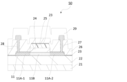
- FIG. 1 is a schematic cross-sectional view of a TFT as an example of the present embodiment
- FIG. FIG. 10 is a schematic cross-sectional view of a TFT of another example of the present embodiment
- FIG. 10 is a schematic cross-sectional view of a TFT of another example of the present embodiment
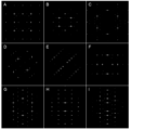
- FIG. 4 is a diagram showing an FFT image of the bixbite structure of In 2 O 3 ; It is a figure for demonstrating the calculation method of lattice-constant a and lattice-constant b.
- FIG. 4 is a diagram showing the result of reciprocal lattice simulation of the bixbite structure of In 2 O 3 ;
- film or “thin film” and the term “layer” can be interchanged depending on the case.
- oxide sintered body may be simply referred to as “sintered body”.
- sputtering target may be simply referred to as “target”.
- electrically connected includes the case of being connected via "something that has some electrical action”.
- something that has some kind of electrical action is not particularly limited as long as it enables transmission and reception of electrical signals between connection objects.
- things having some electrical action include electrodes, wirings, switching elements (such as transistors), resistive elements, inductors, capacitors, and other elements having various functions.
- source and drain functions of a transistor may be interchanged when using transistors with different polarities or when the direction of current changes in circuit operation. Therefore, the terms source and drain can be used interchangeably in this specification and the like.
- x to y represents a numerical range of "x or more and y or less”.
- the upper and lower limits recited for numerical ranges can be arbitrarily combined.
- the form which combined two or more of the individual forms of this invention described below is also the form of this invention.
- the "main surface of the thin film” refers to the surface having the widest area among the surfaces of the thin film.
- a specific plane of a crystal or a plane parallel thereto is referred to as a crystal plane.
- a direction perpendicular to a crystal plane is called a plane orientation.
- the crystal oxide thin film according to the present embodiment is a crystal oxide thin film containing In as a main component. Then, lattice images of a plurality of image regions extracted from a cross-sectional transmission electron microscope image (hereinafter sometimes referred to as a cross-sectional TEM image) of the crystalline oxide thin film are each subjected to two-dimensional Fourier transform (FFT) processing. 50% or more of the obtained Fourier transform image (hereinafter referred to as FFT image) is (100), (110), (111), (211), (411), (125), (210), (310 ), and (320). Note that the multiple image areas are 10 image areas in the following description, but the number of image areas is not limited to 10, and may be a larger number. For example, 50 or more image regions may be extracted.
- FFT image Fourier transform
- a crystalline oxide thin film having the above properties can be obtained not only by the method described in the manufacturing method of a crystalline oxide thin film described later, but also by adjusting the crystal state of the crystalline oxide thin film into a columnar shape.
- the crystalline oxide thin film according to this embodiment contains In element as a main component.
- Being the main component means that the composition ratio of In (atomic %: at %) is 50 at % or more with respect to all metal elements in the crystalline oxide thin film.
- the composition ratio of In is preferably 62 at % or more, more preferably 70 at % or more, more preferably 80 at % or more, and even more preferably 85 at % or more. If 50 at % or more of the total number of metal atoms constituting the crystalline oxide thin film is In element, crystallization easily progresses in the deposited amorphous film, and the crystalline oxide thin film according to the present embodiment. can exhibit sufficiently high mobility when it is employed in a TFT.
- crystalline oxide thin films include H, B, C, N, O, F, Mg, Al, Si, O, S, Cl, Ar, Ca, Sc, Ti, V, Cr, Mn, Fe, Co, Ni, Cu, Zn, Ga, Ge, Y, Zr, Nb, Mo, Tc, Ru, Rh, Pd, Ag, Cd, Sn, Sb, Cs, Ba, Ln, Hf, Ta, W, Re, It may contain one or more elements selected from the group consisting of Os, Ir, Pt, Au, Pb and Bi.
- the crystalline oxide thin film may consist essentially of elements selected from In, Mg, Al, Si, Zn, Ga, Mo, Sn, Ln elements (lanthanoid elements) and O.
- the term “substantially” refers to the range in which the effects of the present invention due to the combination of In, Mg, Al, Si, Zn, Ga, Mo, Sn, Ln and O are produced, and This means that the crystalline oxide thin film may contain other components.
- the metal elements are In and Ga, and the atomic ratio satisfies the following formula (11). [Ga]/([In]+[Ga])] ⁇ 22at% (11)
- F or H may be included in addition to inevitable impurities and O.
- a more preferable second form of the crystalline oxide thin film includes In and B, Al, Sc, Mg, Zn, Ti, Y, Zr, Mo, Sn, Hf, W, Nb, and Ta as metal elements. , Ge, Si, La, Ce, Pr, Nd, Sm, Dy, Ho, Er, Tm, Yb, and Lu.
- the ratio satisfies the following formula (12). [X]/([In]+[X])] ⁇ 15at% (12)
- F or H may be included in addition to inevitable impurities and O.
- the ratio of In increases, and the bixbite structure in which the In site is substituted with X can be crystallized even by annealing at a low temperature such as 300°C. Furthermore, by adding the element X, which has a strong bonding force with oxygen, oxygen vacancies after annealing can be suppressed, and a film stable as a semiconductor can be formed.
- a more preferred third form of the crystalline oxide thin film includes metal elements In, Ga, B, Al, Sc, Mg, Zn, Ti, Y, Zr, Mo, Sn, Hf, W, Consists of one or more elements X selected from Nb, Ta, Ge, Si, La, Ce, Pr, Nd, Sm, Dy, Ho, Er, Tm, Yb and Lu, and metal elements other than In and Ga as additive elements
- X the atomic ratio satisfies the following formulas (13) and (14).
- a more preferred fourth form of the crystalline oxide thin film includes metal elements In, Sn, B, Al, Sc, Mg, Zn, Ti, Y, Zr, Mo, Hf, W, Nb, It consists of one or more elements X selected from Ta, Ge, Si, La, Ce, Pr, Nd, Sm, Dy, Ho, Er, Tm, Yb and Lu, and metal elements other than In and Sn are called element X , the atomic ratio satisfies the following formulas (15) and (16).
- F or H may be included in addition to inevitable impurities and O.
- F or H may be included in addition to inevitable impurities and O.
- the ratio of In is increased, and even with annealing at a low temperature such as 300° C., it is possible to crystallize into a bixbite structure in which the In sites are substituted with Sn. Since Sn has a large ion radius and orbital overlap with In is large, high mobility can be maintained. Further, by adding the additive element X having a strong bonding force with oxygen, the oxygen vacancies after annealing can be further suppressed, and a film stable as a semiconductor can be formed.
- a more preferable fifth form of the crystalline oxide thin film includes In, Zn, B, Al, Sc, Mg, Ti, Y, Zr, Mo, Hf, W, Nb, Ta, It consists of one or more elements X selected from Ge, Si, La, Ce, Pr, Nd, Sm, Dy, Ho, Er, Tm, Yb and Lu, and when the element X is a metal element other than In and Zn , the atomic ratio satisfies the following formulas (17) and (18).
- F or H may be included in addition to inevitable impurities and O.
- F or H may be included in addition to inevitable impurities and O.
- the ratio of In is increased, and the bixbite structure in which the In sites are substituted with Zn can be crystallized even by annealing at a low temperature such as 300.degree.
- Zn the film immediately after the film formation can be made amorphous, and the film can be processed without residue during semiconductor patterning using acid during the fabrication of TFTs.
- an additive element X having a strong bonding force with oxygen oxygen vacancies after annealing can be suppressed, and a film stable as a semiconductor can be formed.
- the content (atomic ratio) of each metal element in the crystalline oxide thin film can be obtained by measuring the abundance of each element by ICP (Inductive Coupled Plasma) measurement or XRF (X-ray Fluorescence) measurement.
- ICP Inductive Coupled Plasma
- XRF X-ray Fluorescence
- ICP-OES inductively coupled plasma emission spectrometer
- a thin-film fluorescent X-ray analyzer AZX400, manufactured by Rigaku Corporation
- the content (atomic ratio) of each metal element in the crystalline oxide thin film was measured by TEM-EDS measurement using an electron microscope, ICP measurement using an inductively coupled plasma emission spectrometer, and sector-type dynamic secondary ion mass measurement. Analysis can be performed with an error accuracy within 2 atomic % by SIMS analysis using an analyzer.
- the metal elements in the crystal oxide thin film are identified by cross-sectional TEM-EDS, and the composition ratio is identified within an error range of about 10 atomic % by semi-quantitative analysis.
- a standard oxide thin film is prepared from 10 kinds of composition ratios with known atomic ratios of metal elements in the range of 20 atomic % from the results of semi-quantitative analysis.
- the value measured by the inductively coupled plasma emission spectrometer or the thin film fluorescence X-ray spectrometer is taken as the absolute value of the composition ratio.
- a source/drain electrode was formed with the same material as the TFT element and with the same channel length.
- the mass spectrum intensity of each element is obtained, and a calibration curve of known element concentrations and mass spectrum intensities is prepared.
- the oxide thin film portion of the actual TFT element taken out from the panel is subjected to SIMS analysis using a sector-type dynamic secondary ion mass spectrometer, and the atomic ratio is calculated from the spectral intensity using the calibration curve described above.
- the calculated atomic ratio can be confirmed with an accuracy within 2 atomic % of the atomic ratio of the oxide thin film separately measured by a thin film fluorescence X-ray spectrometer or an inductively coupled plasma emission spectrometer.
- the lattice images of a plurality of image regions extracted from the cross-sectional TEM image of the crystalline oxide thin film are subjected to two-dimensional Fourier transform (FFT), respectively.
- FFT two-dimensional Fourier transform
- 50% or more of any plane orientation selected from (100), (110), (111), (211), (411), (125), (210), (310), and (320) indicates (100), (110), (111), (211), (411), (125), (210), (310), and (320) are all In 2 O 3 bixbyite crystals.
- a plane and corresponding to one of these plane orientations is referred to as "showing FFT specific plane orientation".
- the crystalline oxide thin film is good and suitable for the FFT channel layer. It can be determined that it has a bixbite crystal structure. As a result, when a crystalline oxide thin film is used as a channel layer of a TFT, high mobility can be exhibited, and fluctuation in threshold voltage (Vth) is small, resulting in excellent reliability.
- Vth threshold voltage
- % or more has any plane orientation selected from (100), (110), (111), (211), (411), (125), (210), (310), and (320) show. More preferably, 100% of the FFT images of the lattice images of the plurality of image regions are (100), (110), (111), (211), (411), (125), (210), (310) , and (320).
- the crystalline oxide thin film according to one embodiment has a lattice constant a in the direction normal to the main surface of the crystalline oxide thin film (hereinafter referred to as the normal direction) for each Fourier transform image showing the FFT specific plane orientation, and the arithmetic mean value of the lattice strains ⁇ 1 , . ⁇ aver is 1.0 ⁇ aver ⁇ 1.1.
- the lattice strain ⁇ indicates the degree of strain in the crystal lattice.
- the lattice constant b in the plane direction is larger than the lattice constant a in the normal direction, A tensile stress is generated in the crystal lattice.
- Vth threshold voltage
- the fluctuation of the threshold voltage (Vth) is small and the reliability is excellent.
- ⁇ aver is preferably 1.01 to 1.09, more preferably 1.02 to 1.08.
- the thickness of the crystalline oxide thin film is 3 nm or more and 130 nm or less.
- the crystals of the crystalline oxide thin film tend to be columnar single-layer crystals. This is because by setting the film thickness to 130 nm or less, it is possible to suppress the progress of crystallization in the oxide thin film formed on the support in the stage before the annealing treatment. This is because it is possible to suppress the inhibition of crystal growth due to the presence of crystals. Therefore, when a crystalline oxide thin film is used as a channel layer of a TFT, high mobility can be exhibited and reliability is excellent.
- the thickness of the crystalline oxide thin film is preferably less than 50 nm, more preferably 45 nm or less, and particularly preferably 40 nm or less.
- the film thickness of the crystalline oxide thin film may be, for example, 5 nm or more, or may be 10 nm or more.
- the film thickness of the crystalline oxide thin film is 3 nm or more, the crystals of the crystalline oxide thin film are less likely to be affected by the underlayer, and a high-quality columnar single-layer crystal is likely to be obtained.
- film thickness is measured based on cross-sectional TEM images.
- the short side length of the crystalline oxide thin film is less than 50 ⁇ m.
- the FFT image of the cross-sectional TEM image of the crystalline oxide thin film tends to exhibit a specific FFT plane orientation.
- the short side length of the crystalline oxide thin film is preferably 45 ⁇ m or less, more preferably 35 ⁇ m or less, even more preferably 25 ⁇ m or less, and particularly preferably 22 ⁇ m or less.
- the length of the short side of the crystalline oxide thin film is, for example, 0.1 ⁇ m or longer, may be 0.3 ⁇ m or longer, or may be 1 ⁇ m or longer.
- the short side By setting the short side to 1 ⁇ m or more, the patterning mask can be aligned with high precision when fabricating a TFT using a crystalline oxide thin film, and stable manufacturing becomes possible. However, since the alignment accuracy of the patterning mask differs in the manufacturing process of integrated circuits and the like, the short side may be less than 1 ⁇ m in that case.
- the average distance D between crystal grain boundaries in the crystalline oxide thin film is preferably 0.01 ⁇ m or more and 2.0 ⁇ m or less.
- the average distance D between crystal grain boundaries in the thin film is measured based on the cross-sectional TEM observation image.
- the average distance D is 5 ⁇ m in the channel direction in an image observed at a magnification of 20,000 using a transmission electron microscope. It is calculated by extracting the central field of view and analyzing the intervals between the crystal grains observed in the cross-sectional TEM image.
- the field of view corresponding to the length in the channel direction may be extracted and calculated in the same manner.
- the crystalline oxide thin film contains crystal grains that have a bixbite structure in the FFT image of the TEM image. Since the crystal grains of the bixbite structure are cubic crystals with good symmetry, it is possible to suppress deterioration of TFT characteristics (mobility) even across crystal grain boundaries.
- the crystalline oxide thin film of the present embodiment uses, for example, a substrate, a buffer layer, an insulating layer, or the like, as a support, such as a lower layer constituting a TFT, and an oxide of In on the support. can be manufactured by forming a thin film containing as a main component and annealing (heat-treating) it at a predetermined temperature.
- the film formation method is not particularly limited, for example, DC sputtering, AC sputtering, RF sputtering, ICP sputtering, reactive sputtering, ion plating, ALD, PLD, MO-CVD, ICP-CVD, sol-gel method, coating method, mist CVD can be mentioned.
- the film When the film is formed by sputtering, the film may be formed using a planar sputtering cathode device, or may be formed using a rotary sputtering cathode device.
- the film can be formed by DC sputtering using a sputtering target containing an oxide sintered body containing an oxide of In as a main component.
- the atomic composition ratio of the crystalline oxide thin film obtained by the sputtering method reflects the atomic composition ratio of the oxide sintered body in the sputtering target. Therefore, it is preferable to form a film using a sputtering target containing an oxide sintered body having an atomic composition ratio similar to that of the desired oxide thin film.
- the target used in the sputtering method preferably has an impurity metal content of 500 ppm or less, more preferably 100 ppm or less.
- the content of impurity metals in the target can be measured by ICP or SIMS as in the case of the crystalline oxide thin film.
- Impurities contained in the target are elements that are not intentionally added and are mixed in raw materials or in the manufacturing process, and are trace elements that do not substantially affect the performance of the target and semiconductor. ” means an element that is a metal element among the elements as “impurities”.
- the method of annealing treatment is not particularly limited, but a hot air furnace, an IR furnace, a lamp annealing device, a laser annealing device, a thermal plasma device, etc. can be used.
- the sputtering target may consist essentially of In and an element selected from Mg, Al, Si, Zn, Ga, Mo, Sn, Ln elements (lanthanoid elements) and O.
- the term “substantially” means that the effects of the present invention due to the combination of Mg, Al, Si, Zn, Ga, Mo, Sn, Ln, and O in addition to the above In are produced in the sputtering target. means that it may contain other ingredients.
- a more preferable first form of the sputtering target is an oxide in which the metal elements are In and Ga, and the atomic ratio is the following formula (11) meet. [Ga]/([In]+[Ga])] ⁇ 22at% (11)
- a more preferred second form of the sputtering target includes In and B, Al, Sc, Mg, Zn, Ti, Y, Zr, Mo, Sn, Hf, W, Nb, Ta, Ge, Si, La, An oxide composed of one or more elements X selected from Ce, Pr, Nd, Sm, Dy, Ho, Er, Tm, Yb, and Lu, where X is a metal element other than In, as an atomic ratio It satisfies the following formula (12). [X]/([In]+[X])] ⁇ 15at% (12)
- a more preferred third form of the sputtering target contains In, Ga, B, Al, Sc, Mg, Zn, Ti, Y, Zr, Mo, Sn, Hf, W, Nb, Ta, Ge, and Si as metal elements. , La, Ce, Pr, Nd, Sm, Dy, Ho, Er, Tm, Yb and Lu. , the atomic ratio satisfies the following formulas (13) and (14). [Ga]/([In]+[Ga]+[X])] ⁇ 22.5 at % (13) [X]/([In]+[Ga]+[X])] ⁇ 8.0at% (14)
- a more preferred fourth form of the sputtering target contains In, Sn, B, Al, Sc, Mg, Zn, Ti, Y, Zr, Mo, Hf, W, Nb, Ta, Ge, Si, and La as metal elements. , Ce, Pr, Nd, Sm, Dy, Ho, Er, Tm, Yb and Lu, where the element X is a metal element other than In and Sn
- the atomic ratio satisfies the following formulas (15) and (16). [Sn]/([In]+[Sn]+[X])] ⁇ 20at% (15) [X]/([In]+[Sn]+[X])] ⁇ 8.0at% (16)
- a more preferred fifth form of the sputtering target contains In, Zn, B, Al, Sc, Mg, Ti, Y, Zr, Mo, Hf, W, Nb, Ta, Ge, Si, La, and Ce as metal elements. , Pr, Nd, Sm, Dy, Ho, Er, Tm, Yb, and Lu.
- the ratio satisfies the following formulas (17) and (18). [Zn]/([In]+[Zn]+[X])] ⁇ 12at% (17) [X]/([In]+[Zn]+[X])] ⁇ 8.0at% (18)
- the thin film is an amorphous oxide thin film. This oxide thin film is patterned into islands by photolithography, and heated and crystallized before forming a protective film, thereby obtaining a crystalline oxide thin film in which surface crystals have a single plane orientation. can. Each step will be described below.
- oxide thin film deposition process In the oxide thin film forming step, the oxide thin film is formed by sputtering using the sputtering target described above.
- the oxide thin film deposition step uses a substrate such as a glass substrate as a support, and includes a buffer layer formed on the support, a buffer layer, and a layer other than the buffer layer such as a metal layer.
- a crystalline oxide thin film is formed directly on the laminated film.
- the buffer layer include SiO 2 , SiN x , Al 2 O 3 and the like. Among these, SiO2 is preferred.
- the gas to be introduced during sputtering film formation is not particularly limited, but examples thereof include argon, nitrogen, oxygen, water, hydrogen, and a mixed gas containing two or more of these gases.
- the flow ratio of oxygen in the mixed gas ((O 2 flow rate) / (Ar flow rate) + (O 2 flow rate))) should be more than 0% and 50% or less. is preferred, and more preferably more than 0% and 20% or less. If the flow ratio of oxygen is more than 0% and 50% or less, the material is easily crystallized into a semiconductor during heating. By changing the oxygen flow ratio, the degree of oxidation of the oxide thin film, that is, the degree of crystallization can be adjusted.
- the flow ratio of oxygen may be appropriately selected as required.
- the flow ratio of water in the mixed gas ((H 2 O flow rate)/(Ar flow rate) + (H 2 O flow rate)) is more than 0.03% and 10% or less. It is preferably more than 0.03% and more preferably 5% or less. If the flow rate ratio of water is more than 0.03% and 5% or less, it will easily crystallize and become a semiconductor when heated. Also, a mixed gas of hydrogen and oxygen may be used instead of water.
- one or more gases selected from the group consisting of argon and oxygen substantially free of impurity gases are used as a sputtering gas to form an oxide thin film.
- a sputtering gas that "substantially does not contain impurity gases” means that gases other than argon and oxygen are excluded, excluding adsorbed water due to gas insertion, and gases that cannot be eliminated (inevitable impurity gases) such as chamber leaks and adsorbed gases. This means that the impurity gas is not actively injected.
- a commercially available mixed gas of high-purity argon and high-purity oxygen can be used as the sputtering gas. Impurities are preferably excluded from the sputter gas if possible.
- the ratio of the impurity gas in the sputtering gas is preferably 0.1% by volume or less, more preferably 0.05% by volume or less. If the proportion of the impurity gas is 0.1% by volume or less, crystallization of the oxide thin film proceeds without problems.
- the purity of high-purity argon and high-purity oxygen is preferably 99% by volume or higher, more preferably 99.9% by volume or higher, and even more preferably 99.99% by volume or higher.
- the sputtering pressure during film formation is not particularly limited as long as the plasma can be stably discharged.
- the FFT image of the cross-sectional TEM image has a high ratio of showing the FFT specific plane orientation, and has a good crystal structure.
- the sputtering target in an RF magnetron sputtering device or a DC magnetron sputtering device for sputtering.
- the oxide thin film before heat treatment preferably contains In element as a main component.
- the oxide thin film before heat treatment preferably contains In element as a main component.
- the oxide thin film in the oxide thin film deposition step, is deposited to a thickness of 3 nm or more and less than 50 nm.
- the reason for setting the thickness of the oxide thin film within the above range is the same as the reason for setting the thickness of the crystalline oxide thin film to 3 nm or more and less than 50 nm.
- the preferred range of the thickness of the oxide thin film is also the same as the preferred range of the thickness of the crystalline oxide thin film.
- the short side length of the oxide thin film is less than 50 ⁇ m.
- the reason why the length of the short side of the oxide thin film is within the above range is the same as the reason why the length of the short side of the crystalline oxide thin film is less than 50 ⁇ m.
- the preferred range of the short side length of the oxide thin film is also the same as the preferred range of the short side length of the crystalline oxide thin film.
- Heat treatment process After forming the oxide thin film, a heat treatment is performed. This heat treatment is sometimes called annealing.
- the temperature of the heat treatment is preferably higher than 300°C and lower than 500°C, preferably 320°C or higher and 480°C or lower, and more preferably 330°C or higher and 450°C or lower. If the heat treatment temperature after the film formation of the oxide thin film is higher than 300° C., the oxide thin film is easily crystallized, and in the crystal oxide thin film finally obtained, the FFT image of the cross-sectional TEM image shows the FFT specific plane orientation. It has a high proportion and a good crystal structure. Also, the average interval D of the crystal grain size can be set within an appropriate range. If the heat treatment temperature after forming the oxide thin film is less than 500° C., the occurrence of cracks and peeling can be suppressed.
- the heating time in the heat treatment step is preferably 0.1 hours or more and 5 hours or less, more preferably 0.3 hours or more and 3 hours or less, and 0.5 hours or more and 2 hours or less. is more preferred. If the heating time in the heat treatment step is 0.1 hour or longer, it is difficult for the oxide thin film to crystallize, and the oxide thin film tends to crystallize. If the heating time in the heat treatment step is 5 hours or less, it is economical.
- the term "heating time” refers to the time (holding time) during which a predetermined maximum temperature is maintained during heat treatment.
- the heating rate in the heat treatment step is preferably 2° C./min or more and 1000° C./min or less, and more preferably 3° C./min or more and 600° C./min or less. If the heating rate in the heat treatment step is 2° C./min or more, the production efficiency of the oxide thin film is improved as compared with the case of less than 1° C./min. If the heating rate in the heat treatment step is 1000° C./min or less, the metal elements are uniformly diffused during crystallization, and crystals in which the metal is not segregated at grain boundaries can be formed. Also, the heating rate in the heat treatment process is a value obtained by dividing the actual temperature of the oxide thin film by time, unlike the value calculated from the set temperature and set time of the furnace. The actual temperature of the oxide thin film can be determined, for example, by measuring an area within 1 cm of the oxide thin film in the furnace with a thermocouple.
- the heat treatment step is preferably carried out in an atmospheric atmosphere at 25°C with a humidity of 10% or more, more preferably 40% or more.
- a humidity of 10% or more When the heat treatment step is performed in the atmosphere with a humidity of 10% or more, hydrogen and oxygen diffuse into the film during annealing, and crystallization can be promoted.
- the upper limit of humidity is not particularly limited, it is generally 80% or less.
- the heat treatment process is preferably performed after patterning the oxide thin film.
- crystallization can be promoted while excess oxygen present in the film during film formation and organic matter adhering during patterning are desorbed.
- the heat treatment process may be performed multiple times. For example, after patterning the oxide thin film, the heat treatment step (first heat treatment step) described above may be performed, and after manufacturing the TFT element, the heat treatment step (second heat treatment step) may be performed as the final step.
- the second heat treatment step is preferably performed at a higher annealing temperature than the first heat treatment step.
- a region having a lower resistance than other regions may be formed in part of the crystalline oxide thin film obtained in the heat treatment step.
- the method for forming the low-resistance region is not particularly limited, but for example, in the presence of indium tin oxide (ITO), aluminum, etc., by using a gate insulating film and/or a gate electrode instead of a mask (self-alignment). , can be formed by reducing the resistance of the target portion of the crystalline oxide thin film by a heat treatment (annealing) method.
- a TFT according to the present embodiment includes the above-described crystalline oxide thin film of the present invention.
- the crystalline oxide thin film of the present invention is used as a channel layer of a TFT.
- the TFT according to this embodiment has a buffer layer and a channel layer, the channel layer being the crystalline oxide thin film, and a gate layer on the opposite side of the channel layer from the buffer layer. It has an insulating film and a gate electrode in this order from the channel layer side.
- a TFT has a substrate, a buffer layer, and a channel layer in that order.
- the TFT has a channel layer, a source electrode and a drain electrode connected to both ends of the channel layer, and a gate electrode stacked on the channel layer with a gate insulating film interposed therebetween. It is a crystalline oxide thin film. That is, the gate insulating film and the gate electrode are provided on the opposite side of the buffer layer as viewed from the channel layer.
- a conventionally known configuration can be adopted as the configuration of the TFT according to the present embodiment.
- the TFT according to the present embodiment includes a step of forming an oxide thin film on a substrate, and a step of annealing the oxide thin film at a temperature exceeding 300° C. in an air atmosphere to form a crystalline oxide thin film. and forming a gate insulating film and a gate electrode on the crystalline oxide thin film in this order.
- the oxide thin film is formed on the buffer layer.
- the TFT according to the present embodiment includes a step of forming an oxide thin film on a substrate, and annealing the oxide thin film at a temperature of over 300° C. in an air atmosphere to form a crystalline oxide thin film. and forming an interlayer insulating film on the crystalline oxide thin film in this order.
- the oxide thin film is formed on the gate insulating film.
- the TFT of the present embodiment includes a step of forming an oxide thin film by sputtering using a sputtering target (sometimes referred to as a film forming step) and a step of heat-treating the oxide thin film (when referred to as a heat treatment step).
- a manufacturing method including The conditions of the film formation process and the heat treatment process are the same as those described above in the method for producing a crystalline oxide thin film.
- the source electrode, drain electrode, gate electrode and gate insulating film can be formed using known materials and forming methods.
- the method of forming each layer other than the crystalline oxide thin film is not particularly limited, and known methods can be used.
- Step of Forming TFT Constituent Layers When forming TFT constituent layers such as an insulating layer on the crystalline oxide thin film, it is preferable to form the constituent layers on the oxide thin film after heat-treating the obtained oxide thin film. . By performing annealing before forming the constituent layers of the TFT, oxygen and hydrogen are diffused at the time of annealing, and high-quality columnar crystals are obtained. A TFT is obtained.
- the shape of the thin film transistor according to this embodiment is not particularly limited, a top gate type transistor, a back channel etch type transistor, an etch stopper type transistor, or the like is preferable. Also, these transistors may be self-aligned.
- FIG. 1 is a schematic cross-sectional view of an example of a TFT according to this embodiment.
- the TFT 50 is a top-gate type TFT, and includes a substrate 21, a buffer layer 22, a channel layer (crystalline oxide thin film) 11, an ITO layer 23, a gate insulating film 24, a gate electrode 25, an interlayer insulating film 26, a source electrode 27, It has a drain electrode 28 and a protective film 29 .
- the TFT 50 has a structure in which a substrate 21, a buffer layer 22, and a channel layer (crystalline oxide thin film) 11 are laminated in this order.
- a high-resistance region 11B is provided in the central portion of the channel layer 11, and a gate insulating film 24 and a gate electrode 25 are laminated in this order on the high-resistance region 11B.
- the gate insulating film 24 is an insulating film that interrupts conduction between the gate electrode 25 and the channel layer (crystalline oxide thin film) 11 .
- Low resistance regions 11A-1 and 11A-2 of the channel layer 11 are present on both sides of the high resistance region 11B.
- the low-resistance regions 11A-1 and 11A-2 and the gate electrode 25 are covered with an ITO layer 23 and an interlayer insulating film 26 .
- the ITO layer 23 is used when forming the low resistance region of the channel layer 11 .
- a source electrode 27 and a drain electrode 28 are connected to the low resistance regions 11A-1 and 11A-2, respectively, through contact holes provided in the ITO layer 23 and the interlayer insulating film 26 .
- the source electrode 27 and the drain electrode 28 are conductive terminals for allowing source current and drain current to flow through the channel layer 11 .
- a protective film 29 is provided so as to cover the TFT constituent layers such as the interlayer insulating film 26 , the source electrode 27 and the drain electrode 28 .
- the buffer layer 22 may consist of a single layer, or may have a laminated structure of two or more layers. Also, a metal layer may be provided between the buffer layer 22 and the substrate 21 . However, it is preferable that the channel layer 11 and the buffer layer 22 are in direct contact as shown in FIG. Materials for forming the buffer layer 22 will be described later. Although the thickness of the buffer layer 22 is not particularly limited, it is, for example, 50 to 600 nm.
- the interlayer insulating film 26 is a single layer in FIG. 1, the interlayer insulating film 26 may have a two-layer structure.
- the TFT of this embodiment can be improved with a known configuration.
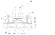
- the TFT 50 may have a light shield layer 31 formed between the substrate 21 and the buffer layer 22, as shown in FIG.
- a light shield layer 31 may be formed as an intermediate layer between layers 22 .
- FIG. 2 is a schematic cross-sectional view of another example of the TFT of this embodiment.
- the TFT 51 has the same configuration as the TFT 50 except that the write shield layer 31 is provided between the substrate 21 and the buffer layer 22 .
- the light shield layer 31 is formed to suppress malfunction of the TFT due to light.
- the write shield layer may be connected to the source electrode 27 or may be connected to the gate electrode 25 .
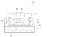
- a configuration example in which the region is the high-resistance region 11B is shown as an example of the TFT of the present invention, but the TFT of the present invention is not limited to this configuration. That is, in the TFT of the present invention, a crystalline oxide thin film having a uniform resistance value in the plane direction may be used as the channel layer 11 . In that case, as shown in FIG. 3, the ITO layer 23 need not be formed.
- FIG. 3 is a schematic cross-sectional view of another example of the TFT of this embodiment.
- the channel layer (crystalline oxide thin film) 11 is a layer having no boundaries of resistance values (the channel layer (crystalline oxide thin film) 11 is not divided into the low resistance region 11A and the high resistance region 11B. ) and that the ITO layer 23 is not provided.
- the crystalline oxide thin film as the channel layer for the source electrode and the drain electrode has a channel length (L length; in FIG. The length in the direction of the source electrode 27-drain electrode 28 in the contact region) is 1 ⁇ m or more and 50 ⁇ m or less, and the channel width (W length; in FIG. The length of the electrode 27-the direction orthogonal to the direction of the drain electrode 28) is 1 ⁇ m or more and 80 ⁇ m or less.
- any commonly used material can be selected.
- a glass substrate, a ceramic substrate, a quartz substrate, a sapphire substrate, or the like can be used.
- a single crystal semiconductor substrate such as silicon or silicon carbide, a polycrystalline semiconductor substrate, a compound semiconductor substrate such as silicon germanium, an SIO (Silicon In Insulator) substrate, or the like, and a semiconductor device can be formed on these substrates. may be used as the substrate.
- a flexible substrate may also be used as the substrate.
- the method of providing a TFT on a flexible substrate in addition to the method of directly fabricating a TFT on a flexible substrate, after fabricating a TFT on a non-flexible substrate, the TFT is peeled off to form a flexible substrate. There is also a method of setting it on the board. In that case, a peeling layer is preferably provided between the non-flexible substrate and the TFT.
- the material for forming the buffer layer is not particularly limited, and generally used materials can be arbitrarily selected, and a laminated film can also be used as the buffer layer.
- the oxidation number of each material may vary.
- the buffer layer 22 can be appropriately designed according to the type of substrate (for example, a glass substrate, a resin substrate such as polyimide).
- a glass substrate for example, a glass substrate, a resin substrate such as polyimide.
- SiO 2 is preferable among the materials mentioned above. If the material of the buffer layer 22 in contact with the channel layer 11 is SiO 2 , the FFT image of the cross-sectional TEM image of the channel layer (thin crystal oxide film) 11 tends to exhibit a specific FFT plane orientation, which is favorable. It has a clear crystal structure.
- a second buffer layer may be placed between the write shield layer 31 and the substrate 21.
- the material for forming the second buffer layer is also not particularly limited, and any commonly used material can be selected.
- a laminated film can also be used as the second buffer layer.
- Materials for the second buffer layer include, for example, SiO2 , SiNx , silicon oxynitride, Al2O3 , Ta2O5 , TiO2 , MgO, ZrO2 , Ga2O3 , GeO2 , Nd2 .
- Materials for forming the gate insulating film are not particularly limited, and commonly used materials can be arbitrarily selected, and a laminated film can also be used as the gate insulating film.
- Materials for forming the drain electrode, the source electrode and the gate electrode are not particularly limited, and commonly used materials can be arbitrarily selected.
- transparent electrodes such as ITO, IZO, ZnO, and SnO2
- metal electrodes such as Al, Ag, Cu, Cr, Ni, Co, Mo, Au, Ti, Zr, Ru, Y, Nb, W, and Ta.
- a metal electrode made of an alloy containing these can be used.
- a laminated electrode having two or more layers can be used.
- each interlayer insulating film Materials for forming each interlayer insulating film are not particularly limited, and generally used materials can be arbitrarily selected.
- a laminated film can be used as an interlayer insulating film.
- the oxidation number of each material may vary.
- the material for forming the light shield layer is not particularly limited, and any commonly used material can be selected. Specifically, metal electrodes such as Al, Ag, Cu, Cr, Ni, Co, Mo, Au, Ti, Zr, Ru, Y, Nb, Ta, W, alloys thereof, laminates thereof, and the like are used. be able to.
- the durability can be easily improved even when the TFT is driven for a long time.
- insulating films such as a buffer layer, a gate insulating film, an interlayer insulating film, and a protective film.
- manufacturing methods include PE-CVD, ALD, PLD, MO-CVD, RF sputtering, ICP sputtering, reactive sputtering, ICP-CVD, ion plating, sol-gel method, coating method, and mist CVD.
- Tetraethoxysilane (TEOS) can also be used as a gas species for PE-CVD in addition to silane (SiH 4 ).
- Insulating films such as a buffer layer, a gate insulating film, an interlayer insulating film, and a protective film often contain an impurity gas immediately after being formed, and are preferably subjected to heat treatment (annealing treatment). By removing the impurity gas by heat treatment, a stable insulating film is obtained, and a highly durable TFT can be easily formed.
- heat treatment annealing treatment
- hydrogen contained in the gate insulating film diffuses to the oxide thin film, and crystal defects present on the surface of the oxide thin film are terminated with hydroxyl groups, resulting in fewer electron traps. Oxide thin films with good conductive properties can be formed.
- the buffer layer for example, RF sputtering, reactive sputtering, PE-CVD, coating method, etc. are preferably used.
- the PE-CVD method can be preferably used because it has high productivity and is a widely used method.
- the saturation mobility of the TFT is preferably 10.0 cm 2 /V ⁇ s or more and 200.0 cm 2 /V ⁇ s or less, more preferably 20.0 cm 2 /V ⁇ s or more and 150.0 cm 2 /V ⁇ s or less. .
- the saturation mobility of the TFT is preferably 10.0 cm 2 /V ⁇ s or more and 200.0 cm 2 /V ⁇ s or less, more preferably 20.0 cm 2 /V ⁇ s or more and 150.0 cm 2 /V ⁇ s or less.
- the saturation mobility of a TFT can be obtained from the transfer characteristics when a drain voltage of 20 V is applied.
- a method for measuring the saturation mobility of a TFT will be described in detail in Examples.
- the threshold voltage (Vth) is preferably ⁇ 3.0 V or more and 3.0 V or less, more preferably ⁇ 2.0 V or more and 2.0 V or less, and even more preferably ⁇ 1.0 V or more and 1.0 V or less. If the threshold voltage (Vth) is ⁇ 3.0 V or more and 3.0 V or less, it is possible to correct Vth to 0 V by mounting a Vth correction circuit on the TFT. When the TFT thus obtained is mounted on a panel, it is possible to drive the display without unevenness in brightness and burn-in. A method for measuring the threshold voltage (Vth) will be described in detail in Examples.
- the on-off ratio is preferably 10 6 or more and 10 12 or less, more preferably 10 7 or more and 10 11 or less, and even more preferably 10 8 or more and 10 10 or less.
- a liquid crystal display can be driven when the on-off ratio is 10 6 or more.
- the on-off ratio is 10 12 or less, it is possible to drive an organic EL device with high contrast.
- the off current can be 10 ⁇ 12 A or less, and when used for the transfer transistor or reset transistor of a CMOS image sensor, the image retention time can be lengthened and the sensitivity can be improved. You can improve it.
- the OFF current value is preferably 10 ⁇ 10 A or less, more preferably 10 ⁇ 11 A or less, and even more preferably 10 ⁇ 12 A or less.
- the off-current value is 10 ⁇ 10 A or less, the organic EL element with high contrast can be driven.
- it is used as a transfer transistor or a reset transistor of a CMOS image sensor it is possible to lengthen the image holding time and improve the sensitivity.
- the leakage current is preferably 1 ⁇ 10 ⁇ 10 A or less, more preferably 1 ⁇ 10 ⁇ 11 A or less, and even more preferably 1 ⁇ 10 ⁇ 12 A or less.
- the crystalline oxide thin film of the channel layer has a high ratio of exhibiting the FFT specific plane orientation. Since it has a high crystalline state, it is possible to exhibit good TFT characteristics in which leakage current is suppressed as described above.
- the leak current is 1 ⁇ 10 ⁇ 10 A or less, an organic EL element with high contrast can be driven.
- it is used as a transfer transistor or a reset transistor of a CMOS image sensor, it is possible to lengthen the image holding time and improve the sensitivity. A method for measuring leakage current will be described in detail in Examples.
- the TFT according to the present embodiment can be suitably used in electronic devices such as display elements such as solar cells, liquid crystal elements, organic electroluminescence elements and inorganic electroluminescence elements, power semiconductor elements, and touch panels.
- display elements such as solar cells, liquid crystal elements, organic electroluminescence elements and inorganic electroluminescence elements, power semiconductor elements, and touch panels.
- the thin film transistor according to this embodiment can also be applied to various integrated circuits such as field effect transistors, logic circuits, memory circuits, and differential amplifier circuits, and can be applied to electronic devices and the like. Furthermore, the thin film transistor according to the present embodiment can be applied not only to a field effect transistor but also to an electrostatic induction transistor and a Schottky barrier transistor.
- the thin film transistor according to this embodiment can be suitably used for a display device such as a portable display device or an in-vehicle display device, a solid-state imaging device, and the like.
- the thin film transistor according to the present embodiment can also be suitably used as a transistor for a flat panel detector for an X-ray image sensor for medical use.
- the crystalline oxide thin film according to this embodiment can also be applied to Schottky diodes, resistance change memories, and resistance elements.
- Example 1 The thin film transistor 50 shown in FIG. 1 was manufactured by the following steps. (1-1) Formation of buffer layer (SiO x layer) (sputtering) Using a SiO 2 sputtering target, a 300 nm-thick SiO x layer (buffer layer) was formed by sputtering on a 4-inch diameter non-alkali glass substrate (support) 21 (EAGLE XG manufactured by Corning). Sputtering conditions are as follows.
- Substrate temperature 25°C Ultimate pressure: 8.5 ⁇ 10 ⁇ 5 Pa
- Atmospheric gas Ar Sputtering pressure (total pressure): 0.4 Pa
- Input voltage RF300W Distance between S (substrate) and T (target): 70mm
- the oxide thin film was patterned into islands by photolithography to form a channel layer.
- a photoresist film was formed on the oxide thin film.
- AZ1500 manufactured by AZ Electronic Materials
- Exposure was performed through a photomask having a pattern having the long side and short side sizes shown in Table 1. After exposure, it was developed with tetramethylammonium hydroxide (TMAH). After development, the oxide thin film was etched with oxalic acid (Kanto Kagaku ITO-06N). After etching, the photoresist was removed to obtain a substrate with a patterned oxide thin film (channel layer). Table 1 shows the sizes of the long and short sides of the obtained channel layer.
- TMAH tetramethylammonium hydroxide
- the substrate with the channel layer formed thereon was placed in a furnace, heated to 350° C. at a rate of 10° C./min in the atmosphere, and held for 1 hour. After holding the inside of the furnace at 350° C. for 1 hour, it was allowed to cool naturally, and after the temperature inside the furnace returned to room temperature, the substrate was taken out from the furnace.
- a 10 nm-thick SiO x layer (first gate insulating film) was formed by sputtering using a SiO 2 sputtering target.
- Sputtering conditions are as follows. Substrate temperature: 25°C Ultimate pressure: 8.5 ⁇ 10 ⁇ 5 Pa Atmosphere gas: mixed gas of Ar + O 2 (O 2 flow rate 30%) Sputtering pressure (total pressure): 0.4 Pa Input voltage: RF100W Distance between S (substrate) and T (target): 70mm
- Second Gate Insulating Film a 100 nm-thick SiO x layer (second gate insulating film) was formed by sputtering using a SiO 2 sputtering target.
- Sputtering conditions are as follows. Substrate temperature: 25°C Ultimate pressure: 8.5 ⁇ 10 ⁇ 5 Pa Atmosphere gas: mixed gas of Ar + O 2 (O 2 flow rate 30%) Sputtering pressure (total pressure): 0.4 Pa Input voltage: RF100W Distance between S (substrate) and T (target): 70mm
- the total thickness of the gate insulating film layers composed of the first and second gate insulating films was 110 nm.
- the gate insulating film layer was etched with buffered hydrofluoric acid (BHF) and patterned into an island shape.
- BHF buffered hydrofluoric acid
- the region where the channel layer is exposed was etched by a film thickness of 10 nm and washed.
- the dimensions of the obtained gate electrode layer and gate insulating layer were 10 ⁇ m in width ⁇ length (size of short side of channel layer ( ⁇ m)+8 ( ⁇ m)).
- the substrate was placed in a furnace, heated to 350°C at 10°C/min in the atmosphere, held for 1 hour, and annealed. After holding the inside of the furnace at 350° C. for 1 hour, it was allowed to cool naturally. After the temperature inside the furnace returned to room temperature, the substrate was taken out of the furnace.
- Substrate temperature 25°C Ultimate pressure: 8.5 ⁇ 10 ⁇ 5 Pa
- Atmospheric gas Ar Sputtering pressure (total pressure): 0.4 Pa
- Input voltage DC100W Distance between S (substrate) and T (target): 70mm
- SA-TG type TFT self-aligned top-gate structure small TFT
- the final shape of the obtained element had a channel length (also referred to as L length, hereinafter referred to as channel length) of 10 ⁇ m, and a channel width of the channel layer shown in Table 1. The length was the same as the short side size ( ⁇ m).
- Examples 2-6 A TFT was fabricated in the same manner as in Example 1, except that the film thickness of the channel layer, the size of the short side, and the method of forming the buffer layer were changed as shown in Table 1.
- the buffer layers of Examples 2 and 4 were formed by the following method.
- Examples 7-11 A TFT was fabricated in the same manner as in Example 1, except that the channel layer deposition conditions, film thickness, short side size, and buffer layer formation method were changed as shown in Table 2. The formation of the buffer layer of Example 8 was performed in the same manner as in Example 2. Moreover, the buffer layer of Example 11 was formed by the following method.
- a SiN x film having a thickness of 300 nm was formed by PE-CVD.
- the deposition conditions were a substrate temperature of 350° C., a deposition pressure of 0.5 Torr, a N 2 /SiH 4 gas flow rate ratio of 100, and an RF power of 200 W.
- Example 1 was different from Example 1 except that the composition ratio of the sputtering target used for forming the channel layer, the film forming conditions for the channel layer, the annealing conditions, the film thickness of the channel layer, and the method for forming the buffer layer were changed as shown in Table 3.
- a TFT was fabricated in the same manner.
- the buffer layers of Examples 13 and 15 were formed in the same manner as in Example 2.
- the formation of the buffer layer of Example 14 was performed by the following method.
- Al 2 O 3 film Formation of buffer layer (Al 2 O 3 film) (ALD; Atomic Layer Deposition) Using trimethylaluminum (Al(CH 3 ) 3 ) and water (H 2 O) as raw material gases, an Al 2 O 3 film with a thickness of 100 nm was formed by ALD at a substrate temperature of 300°C. The film formation was carried out by performing 1000 cycles of a process of introducing trimethylaluminum into the film forming chamber and then purging with nitrogen, then introducing water and then purging with nitrogen.
- ALD Atomic Layer Deposition
- Comparative Examples 1-8 The composition ratio of the sputtering target used for the deposition of the channel layer, the deposition conditions of the channel layer, the annealing conditions, the film thickness of the channel layer, the size of the long side or the short side, and the method of forming the buffer layer were changed as shown in Table 4.
- a TFT was fabricated in the same manner as in Example 1, except that the The formation of the buffer layers in Comparative Examples 1 and 3 was carried out in the same manner as in Example 2.
- a Si substrate with a 100 nm thick thermal oxide film was used as the substrate, and this thermal oxide film (100 nm thick) was used as the buffer layer.
- the Si substrate with a thermal oxide film is obtained by placing the Si substrate in a heating furnace with an oxygen-containing atmosphere and heating the furnace at a temperature of about 900 to 1100° C. for a predetermined time.
- Examples 18-225, Comparative Example 9 Tables 5 to 19 show the composition ratio of the sputtering target used for forming the channel layer, the conditions for forming the channel layer, the film thickness of the channel layer, the sizes of the short and long sides, the annealing conditions, and the method of forming the buffer layer.
- a TFT was fabricated in the same manner as in Example 1, except that the procedure was changed as follows.
- an FIB (FB2100 type” manufactured by Hitachi High-Technologies Corporation) device was used to insert an ion beam in the direction perpendicular to the surface of the channel layer, and an acceleration voltage of 40 kV was applied to test a size of 16 ⁇ m ⁇ 4 ⁇ m. A piece was sampled. After that, from the sampled test piece, a sample was extracted from the region where the gate electrode, the gate insulating film, and the oxide thin film overlapped in the channel length direction (horizontal direction in the drawing).
- the extracted sample was subjected to FIB ("JIB-4700F” manufactured by JEOL Ltd.) until the thickness of the thin piece was about 100 nm in the channel width direction (depth direction in the drawing) perpendicular to the channel length direction and the film thickness direction. type”) apparatus at an acceleration voltage of 20 kV to reduce the thickness of the sample.
- the cross-sectional TEM image was observed using a transmission electron microscope ("JEM-F200” manufactured by JEOL Ltd.) under the condition that the substrate was flat and no external force was applied. Observation was performed at an acceleration voltage of 200 kV and a magnification described later.
- the average distance D when observing the cross section of the oxide thin film can be calculated by analyzing the distance between crystal grains observed by cross-sectional TEM. From the image observed at an observation magnification of 20,000 times, a field of view centered on the central portion in the channel length direction in the thin film TFT with a size of 5 ⁇ m in the channel length direction and the size of the oxide film thickness in the thin film TFT was extracted, and a cross-sectional TEM image was obtained. Observed. The field of view of the obtained cross-sectional TEM image was subjected to image analysis using Image Metrology's "SPIP, Version 4.3.2.0" to calculate the average interval D of the crystal grain boundaries. Details are as follows.
- Lines of color codes H0, S0, and V10 were drawn on the grain boundaries of the cross-sectional TEM image. Further, the contrast was quantified using image analysis software, and the height of (maximum density - minimum density) x 1/4 was set as the threshold. Next, a region exhibiting a contrast equal to or lower than the threshold value was defined as a grain boundary, and the distance between each grain boundary and the closest grain was obtained and used as the grain boundary distance. The average distance D between grain boundaries was obtained by dividing the obtained total distance between grain boundaries by the number of locations where the distance was measured. In the later-described (b) evaluation of the crystal state, those judged to be “two-layered crystals” were not measurable because the grain boundaries of the columnar crystals could not be analyzed.
- (b) Crystalline State The crystalline state was determined by observing the electron beam diffraction pattern of the sample obtained by observing the cross-sectional TEM image. Specifically, using an electron microscope ("JEM-F200 type” manufactured by JEOL Ltd.), the area of the oxide thin film observed at a cross-sectional TEM image at a magnification of 1,000,000 times is irradiated with a selected area aperture. An electron beam was irradiated with a diameter of about 100 nm and an acceleration voltage of 200 kV, and the diffraction pattern was measured. Ten fields of view were extracted at approximately equal intervals so that the observation points did not overlap in the range of 10 ⁇ m in the channel length direction in the cross-sectional TEM image sample.
- JEM-F200 type manufactured by JEOL Ltd.
- FFT Specific Plane Orientation Ratio The FFT specific plane orientation ratio is obtained by performing two-dimensional Fourier transformation (FFT: Fast Fourier Transformation) on a TEM image obtained by observing a cross-sectional TEM image, and reciprocal lattice simulation results. calculated by comparing with FFT images were acquired by performing calculations using software ImageJ (free software ver1.45l (2011/07/20)). Software ReciPro (free software ver4.797 (2021/03/24)) was used for the simulation, and reciprocal lattice simulation and TEM image simulation of the bixbite structure of In 2 O 3 were performed.
- FFT Fast Fourier Transformation
- ICSD Inorganic Crystal Structure Database
- ICSD Inorganic Crystal Structure Database
- the simulation was performed in a range in which reciprocal lattice points with an interplanar spacing of at least 0.8 ⁇ were displayed, and the results were obtained with the same image size in both the vertical and horizontal sizes.
- FIG. 4 shows an FFT image obtained by two-dimensional Fourier transform of the TEM image simulation result of the bixbite structure of In 2 O 3 .
- the TEM image was taken from the oxide thin film area observed in the cross-sectional TEM image at an observation magnification of 1,000,000 times, and 10 fields of view were taken at approximately equal intervals in a range of 10 ⁇ m in the channel length direction so that the observation points do not overlap. Extracted.
- the FFT image of each field of view extracted is scaled within a range where the size of the frequency domain is ⁇ 10% error from the reciprocal lattice simulation so that the aspect ratio of the image does not change, and then this FFT image is rotated in the direction of the two-dimensional plane of the image, and the FFT image adjusted in size and inclination is superimposed so that the center of the reciprocal lattice simulation and the image coincide. Then, on the crystal plane of any of the patterns A to I, when the coordinates of 8 or more points match in order from the brightest bright point in the FFT image to the brightest bright point, the field of view is the FFT specific plane orientation. It was determined that there is.
- the crystal plane of A shown in FIG. 4 is (100), and has the property of four-fold symmetry in which the patterns match when the central coordinates of the image are fixed and rotated by 90°.
- the typical spacings of bright spots are 2.53 ⁇ , 1.79 ⁇ , and 1.27 ⁇ , and bright spots with the same spacing are present at 90° rotated positions.
- the 1.79 ⁇ bright spot is on the coordinate axis rotated 45.0° from the 2.53 ⁇ bright spot, and the 1.27 ⁇ bright spot is on the same coordinate axis as the 2.53 ⁇ bright spot.
- the crystal plane of B shown in FIG. 4 is (110), and has a two-fold symmetry property in which the patterns match when the central coordinates of the image are fixed and rotated by 180°.
- the typical spacings of bright spots are 2.53 ⁇ , 2.92 ⁇ , 1.79 ⁇ , and 1.27 ⁇ , and bright spots with the same spacing are present at 180° rotation positions.
- the 1.27 ⁇ bright spot is on the same coordinate axis as the 2.53 ⁇ bright spot.
- the crystal plane of C shown in FIG. 4 is (111), and has the property of 6-fold symmetry in which the patterns match when the central coordinates of the image are fixed and rotated by 60°.
- the typical spacing between bright spots is 1.79 ⁇ and 1.03 ⁇ , and bright spots with the same spacing are present at positions rotated by 60°.
- the crystal plane of D shown in FIG. 4 is (211), and has a two-fold symmetry property in which the patterns match when the central coordinates of the image are fixed and rotated by 180°.
- the typical spacings of bright spots are 2.92 ⁇ , 1.53 ⁇ , 1.79 ⁇ , and 1.46 ⁇ , and bright spots with the same spacing are present at 180° rotation positions.
- the 1.46 ⁇ bright spot is on the same coordinate axis as the 2.92 ⁇ bright spot.
- the crystal plane of E shown in FIG. 4 is (411), and has two-fold symmetry in which the patterns match when the central coordinates of the image are fixed and rotated by 180°.
- the typical spacings of bright spots are 1.79 ⁇ , 1.53 ⁇ , 1.69 ⁇ , and 0.89 ⁇ , and bright spots with the same spacing are present at 180° rotation positions.
- the 0.89 ⁇ bright spot is on the same coordinate axis as the 1.79 ⁇ bright spot.
- the crystal plane of F shown in FIG. 4 is (125), and has a two-fold symmetry property in which the patterns match when the central coordinates of the image are fixed and rotated by 180°.
- the typical spacings of bright spots are 2.26 ⁇ , 1.53 ⁇ , 2.07 ⁇ , and 1.38 ⁇ , and bright spots with the same spacing are present at 180° rotation positions.
- the 1.38 ⁇ bright spot is on the same coordinate axis as the 2.07 ⁇ bright spot.
- the crystal plane of G shown in FIG. 4 is (210), and it has two-fold symmetry in which the patterns match when the central coordinates of the image are fixed and rotated by 180°.
- the typical spacings of bright spots are 2.53 ⁇ , 2.07 ⁇ , 2.26 ⁇ , and 1.27 ⁇ , and bright spots with the same spacing are present at positions rotated by 180°.
- the 1.27 ⁇ bright spot is on the same coordinate axis as the 2.53 ⁇ bright spot.
- 2 bright spots with an interplanar spacing of 2.53 ⁇ 4 bright spots with an interplanar spacing of 2.07 ⁇ , 2 bright spots with an interplanar spacing of 2.26 ⁇ , and 2 bright spots with an interplanar spacing of 1.27 ⁇ , arbitrarily selected from a total of 10 points, and confirmed whether or not the coordinates match.
- the crystal plane of H shown in FIG. 4 is (310), and has a two-fold symmetry property in which the patterns match when the central coordinates of the image are fixed and rotated by 180°.
- the typical spacings of bright spots are 2.53 ⁇ , 2.71 ⁇ , 1.60 ⁇ , and 1.27 ⁇ , and bright spots with the same spacing are present at positions rotated by 180°.
- the 1.27 ⁇ bright spot is on the same coordinate axis as the 2.53 ⁇ bright spot.
- the crystal plane of I shown in FIG. 4 is (320), and has two-fold symmetry in which the patterns match when the central coordinates of the image are fixed and rotated by 180°.
- the typical spacings of bright spots are 2.53 ⁇ , 2.16 ⁇ , and 2.71 ⁇ , and bright spots with the same spacing are present at 180° rotation positions.
- the state of two-layer crystallization in the film thickness direction of the oxide thin film is not included.
- the largest area was extracted, and the area was evaluated in the same manner as described above as to whether or not it had the FFT specific plane orientation.
- the FFT images of the 10 extracted fields of view are compared with the simulation patterns (patterns A to I), and the number of fields determined to be the FFT specific plane orientation is the total number of fields observed (10 ) to calculate the FFT specific plane orientation ratio (%) by ((the number of fields of view indicating the FFT specific plane orientation)/(the number of total fields of view)).
- ⁇ (lattice strain) The average value of ⁇ (lattice strain) was calculated from the lattice constant obtained by analyzing the FFT image of the cross-sectional TEM image.
- ⁇ (lattice distortion) is a lattice obtained by analyzing each FFT image for each of the 10 fields of view extracted in "(c) FFT specific plane orientation ratio" and determined to correspond to the FFT specific plane orientation. Calculated from constants. Each visual field was observed under the condition that the angle difference between the corresponding plane orientation and the axis in the observation direction was 1° or less.
- the lattice constant was calculated from the FFT image obtained from the TEM image of the lattice image observed at an observation magnification of 1,000,000 (see FIG. 5).
- the TEM image includes the layer in contact with the crystalline oxide thin film, and the direction parallel to the interface of the crystalline oxide thin film on the alkali-free glass substrate (support) side (that is, the direction parallel to the main surface of the crystalline oxide thin film. , plane direction) and a direction perpendicular to the interface of the crystalline oxide thin film on the non-alkali glass substrate (support) side (that is, a normal direction to the main surface of the crystalline oxide thin film.
- the normal direction and were adopted so that they can be clearly specified.
- a two-dimensional Fourier transform process is performed on a pixel area of 512 pixels x 512 pixels or more and a pixel area of 10 nm x 10 nm or more, which does not include grain boundaries or adjacent layers of the crystalline oxide thin film, FFT images were acquired.
- the obtained FFT image was smoothed with a Gaussian filter to remove noise, and the vertex coordinates with the highest luminance among the bright points were extracted and used as the coordinates of the reciprocal lattice points.
- the vertex coordinates showing the highest brightness among the bright points positioned on the coordinate axis extending in the normal direction from the central coordinates of the FFT image were taken as the reciprocal lattice point P1.
- the vertex coordinates showing the highest brightness among the bright points positioned on the coordinate axis extending in the plane direction from the center coordinates of the FFT image were taken as the reciprocal lattice point P2.
- the sizes of the frequency regions (distances from the center coordinates of the FFT image) corresponding to these reciprocal lattice points P1 and P2 were defined as surface spacing d1 and surface spacing d2, respectively.
- the interplanar spacing was obtained by converting the size of the frequency domain into the length of the real space.
- a reciprocal lattice simulation of the bixbite structure of In 2 O 3 was performed, and the simulation result of the obtained reciprocal lattice pattern (Fig. 6 The pattern corresponding to any one of the patterns A to I and the Miller indices of each bright point) is compared with the pattern of the FFT image to be analyzed, and the Miller indices of the reciprocal lattice point P1 (h 1 , k 1 , l 1 ), and the Miller indices (h 2 , k 2 , l 2 ) of the reciprocal lattice point P2.
- each bright point in the FFT image has a bright point at a position rotated 180° from the central coordinate, and has the same surface spacing and opposite sign of the Miller index, but it affects the calculation result of the lattice constant. Therefore, either positive or negative Miller indices may be used.
- the lattice constant a in the normal direction was calculated by the following formula (1) from the interplanar spacing d1 of the reciprocal lattice point P1 and the Miller indices (h 1 , k 1 , l 1 ).
- the lattice constant b in the planar direction was calculated from the interplanar spacing d2 of the reciprocal lattice point P2 and the Miller indices (h 2 , k 2 , l 2 ) by the following equation (2).
- the reciprocal lattice point P1 exists on a coordinate axis extending from the center coordinates of the FFT image, the angle formed with the normal direction is in the range of ⁇ 30°, and the interplanar spacing d1 is 0.
- the bright spots in the range of 0.8 to 2.0 ⁇ the bright spots showing the highest brightness at an angle closer to the substrate normal were selected.
- the reciprocal lattice point P2 is, specifically, a coordinate axis extending from the center coordinates of the FFT image, exists on a coordinate axis that forms an angle with the plane direction within a range of ⁇ 30°, and has a surface interval d2 of Among the bright spots in the range of 0.8 to 2.0 ⁇ , the bright spots showing the highest brightness at an angle closer to the substrate plane were selected.
- the reciprocal lattice point P1 and the reciprocal lattice point P2 are arranged so that the angle ⁇ between the coordinate axis on which the reciprocal lattice point P1 exists and the coordinate axis on which the reciprocal lattice point P2 exists is in the range of 70° ⁇ 110°. , the bright spots P1 and P2 were selected.
- Lattice strain ⁇ was calculated from the lattice constant a in the normal direction and the lattice constant b in the plane direction by the following formula (3).
- the average value ⁇ aver of ⁇ (lattice distortion) calculated for each field of view was calculated by arithmetic mean.
- PBTS positive bias heating stress test
- NBTS negative bias heating stress test
- CCS constant current stress test
- Vg +20 V was applied to the PBTS at 50° C., and the threshold voltage (Vth) after 10,000 seconds had passed was compared with that before the test, and the difference was defined as ⁇ Vth.
- Vg -20 V was applied at 50° C., and the threshold voltage (Vth) after 10,000 seconds had passed was compared with that before the test, and the difference was defined as ⁇ Vth.
- the crystalline oxide thin film of the present invention can be suitably used as a component of a thin film transistor, such as a channel layer.
- the thin film transistor of the present invention can be used in electronic circuits used in electrical equipment, electronic equipment, vehicles, and power engines.
Landscapes
- Chemical & Material Sciences (AREA)
- Chemical Kinetics & Catalysis (AREA)
- Engineering & Computer Science (AREA)
- Materials Engineering (AREA)
- Mechanical Engineering (AREA)
- Metallurgy (AREA)
- Organic Chemistry (AREA)
- Thin Film Transistor (AREA)
- Recrystallisation Techniques (AREA)
Priority Applications (5)
| Application Number | Priority Date | Filing Date | Title |
|---|---|---|---|
| JP2023554577A JPWO2023063352A1 (cg-RX-API-DMAC7.html) | 2021-10-14 | 2022-10-12 | |
| US18/700,706 US20250151354A1 (en) | 2021-10-14 | 2022-10-12 | Crystalline oxide thin film, method for producing same, thin film transistor, and method for producing same |
| KR1020247011836A KR20240074786A (ko) | 2021-10-14 | 2022-10-12 | 결정 산화물 박막 및 그 제조 방법, 그리고 박막 트랜지스터 및 그 제조 방법 |
| EP22881047.9A EP4418309A4 (en) | 2021-10-14 | 2022-10-12 | Thin film of crystal oxide, its production process, thin film transistor and its production process |
| CN202280068555.2A CN118103963A (zh) | 2021-10-14 | 2022-10-12 | 晶体氧化物薄膜及其制造方法、以及薄膜晶体管及其制造方法 |
Applications Claiming Priority (4)
| Application Number | Priority Date | Filing Date | Title |
|---|---|---|---|
| JP2021-169157 | 2021-10-14 | ||
| JP2021169157 | 2021-10-14 | ||
| JP2022053861 | 2022-03-29 | ||
| JP2022-053861 | 2022-03-29 |
Publications (1)
| Publication Number | Publication Date |
|---|---|
| WO2023063352A1 true WO2023063352A1 (ja) | 2023-04-20 |
Family
ID=85988661
Family Applications (1)
| Application Number | Title | Priority Date | Filing Date |
|---|---|---|---|
| PCT/JP2022/038044 Ceased WO2023063352A1 (ja) | 2021-10-14 | 2022-10-12 | 結晶酸化物薄膜及びその製造方法、並びに薄膜トランジスタ及びその製造方法 |
Country Status (6)
| Country | Link |
|---|---|
| US (1) | US20250151354A1 (cg-RX-API-DMAC7.html) |
| EP (1) | EP4418309A4 (cg-RX-API-DMAC7.html) |
| JP (1) | JPWO2023063352A1 (cg-RX-API-DMAC7.html) |
| KR (1) | KR20240074786A (cg-RX-API-DMAC7.html) |
| TW (1) | TW202332043A (cg-RX-API-DMAC7.html) |
| WO (1) | WO2023063352A1 (cg-RX-API-DMAC7.html) |
Cited By (1)
| Publication number | Priority date | Publication date | Assignee | Title |
|---|---|---|---|---|
| WO2026154307A1 (ja) * | 2025-01-15 | 2026-07-23 | 株式会社半導体エネルギー研究所 | 金属酸化物層の形成方法、金属酸化物層、半導体装置 |
Citations (5)
| Publication number | Priority date | Publication date | Assignee | Title |
|---|---|---|---|---|
| JPH09282945A (ja) * | 1996-04-16 | 1997-10-31 | Idemitsu Kosan Co Ltd | 透明導電膜およびその製造方法 |
| JP2013201211A (ja) * | 2012-03-23 | 2013-10-03 | Sony Corp | 薄膜トランジスタ、薄膜トランジスタの製造方法および電子機器 |
| JP5491258B2 (ja) | 2010-04-02 | 2014-05-14 | 出光興産株式会社 | 酸化物半導体の成膜方法 |
| KR20210027580A (ko) * | 2019-08-28 | 2021-03-11 | 한양대학교 산학협력단 | 빅스비아이트 결정을 함유하는 금속 산화물 채널층을 구비하는 박막트랜지스터 및 수직형 비휘발성 메모리 소자 |
| JP6853421B2 (ja) | 2019-03-28 | 2021-03-31 | 出光興産株式会社 | 結晶酸化物薄膜、積層体及び薄膜トランジスタ |
Family Cites Families (1)
| Publication number | Priority date | Publication date | Assignee | Title |
|---|---|---|---|---|
| JPS5491258U (cg-RX-API-DMAC7.html) | 1977-12-09 | 1979-06-28 |
-
2022
- 2022-10-12 KR KR1020247011836A patent/KR20240074786A/ko active Pending
- 2022-10-12 US US18/700,706 patent/US20250151354A1/en active Pending
- 2022-10-12 WO PCT/JP2022/038044 patent/WO2023063352A1/ja not_active Ceased
- 2022-10-12 JP JP2023554577A patent/JPWO2023063352A1/ja active Pending
- 2022-10-12 EP EP22881047.9A patent/EP4418309A4/en active Pending
- 2022-10-14 TW TW111139023A patent/TW202332043A/zh unknown
Patent Citations (5)
| Publication number | Priority date | Publication date | Assignee | Title |
|---|---|---|---|---|
| JPH09282945A (ja) * | 1996-04-16 | 1997-10-31 | Idemitsu Kosan Co Ltd | 透明導電膜およびその製造方法 |
| JP5491258B2 (ja) | 2010-04-02 | 2014-05-14 | 出光興産株式会社 | 酸化物半導体の成膜方法 |
| JP2013201211A (ja) * | 2012-03-23 | 2013-10-03 | Sony Corp | 薄膜トランジスタ、薄膜トランジスタの製造方法および電子機器 |
| JP6853421B2 (ja) | 2019-03-28 | 2021-03-31 | 出光興産株式会社 | 結晶酸化物薄膜、積層体及び薄膜トランジスタ |
| KR20210027580A (ko) * | 2019-08-28 | 2021-03-11 | 한양대학교 산학협력단 | 빅스비아이트 결정을 함유하는 금속 산화물 채널층을 구비하는 박막트랜지스터 및 수직형 비휘발성 메모리 소자 |
Non-Patent Citations (1)
| Title |
|---|
| See also references of EP4418309A4 |
Cited By (1)
| Publication number | Priority date | Publication date | Assignee | Title |
|---|---|---|---|---|
| WO2026154307A1 (ja) * | 2025-01-15 | 2026-07-23 | 株式会社半導体エネルギー研究所 | 金属酸化物層の形成方法、金属酸化物層、半導体装置 |
Also Published As
| Publication number | Publication date |
|---|---|
| EP4418309A1 (en) | 2024-08-21 |
| TW202332043A (zh) | 2023-08-01 |
| JPWO2023063352A1 (cg-RX-API-DMAC7.html) | 2023-04-20 |
| US20250151354A1 (en) | 2025-05-08 |
| KR20240074786A (ko) | 2024-05-28 |
| EP4418309A4 (en) | 2025-11-05 |
Similar Documents
| Publication | Publication Date | Title |
|---|---|---|
| US12205992B2 (en) | Crystalline oxide thin film, multilayer body and thin film transistor | |
| KR101659054B1 (ko) | 반도체 소자의 제조 방법 | |
| WO2023063348A1 (ja) | 結晶酸化物薄膜、積層体及び薄膜トランジスタ | |
| JP2015032655A (ja) | 薄膜トランジスタ | |
| US20250151354A1 (en) | Crystalline oxide thin film, method for producing same, thin film transistor, and method for producing same | |
| WO2024219464A1 (ja) | 半導体デバイス及び電子機器 | |
| US20250338563A1 (en) | Laminate structure and thin film transistor | |
| US20250351458A1 (en) | Laminate structure and thin film transistor | |
| CN118103994A (zh) | 晶体氧化物薄膜、层叠体及薄膜晶体管 | |
| CN118103963A (zh) | 晶体氧化物薄膜及其制造方法、以及薄膜晶体管及其制造方法 | |
| WO2016035503A1 (ja) | 薄膜トランジスタ | |
| US20250374609A1 (en) | Laminate structure and thin film transistor | |
| KR102944325B1 (ko) | 박막 트랜지스터 및 전자 기기 | |
| WO2026014513A1 (ja) | 結晶酸化物膜、薄膜トランジスタ及び電子機器 | |
| TWI899892B (zh) | 薄膜電晶體及電子機器 | |
| KR102944064B1 (ko) | 박막 트랜지스터 및 전자 기기 | |
| TWI899894B (zh) | 氧化物半導體膜、積層結構體、薄膜電晶體、及電子機器 | |
| TWI899893B (zh) | 薄膜電晶體及電子機器 | |
| TW202531896A (zh) | 氧化物半導體膜、薄膜電晶體、及電子機器 |
Legal Events
| Date | Code | Title | Description |
|---|---|---|---|
| 121 | Ep: the epo has been informed by wipo that ep was designated in this application |
Ref document number: 22881047 Country of ref document: EP Kind code of ref document: A1 |
|
| ENP | Entry into the national phase |
Ref document number: 20247011836 Country of ref document: KR Kind code of ref document: A |
|
| WWE | Wipo information: entry into national phase |
Ref document number: 202280068555.2 Country of ref document: CN |
|
| ENP | Entry into the national phase |
Ref document number: 2023554577 Country of ref document: JP Kind code of ref document: A |
|
| WWE | Wipo information: entry into national phase |
Ref document number: 2022881047 Country of ref document: EP |
|
| NENP | Non-entry into the national phase |
Ref country code: DE |
|
| ENP | Entry into the national phase |
Ref document number: 2022881047 Country of ref document: EP Effective date: 20240514 |
|
| WWP | Wipo information: published in national office |
Ref document number: 18700706 Country of ref document: US |