WO2023063046A1 - Nitride semiconductor substrate and manufacturing method therefor - Google Patents
Nitride semiconductor substrate and manufacturing method therefor Download PDFInfo
- Publication number
- WO2023063046A1 WO2023063046A1 PCT/JP2022/035314 JP2022035314W WO2023063046A1 WO 2023063046 A1 WO2023063046 A1 WO 2023063046A1 JP 2022035314 W JP2022035314 W JP 2022035314W WO 2023063046 A1 WO2023063046 A1 WO 2023063046A1
- Authority
- WO
- WIPO (PCT)
- Prior art keywords
- layer
- substrate
- crystal silicon
- nitride semiconductor
- single crystal
- Prior art date
Links
- 239000000758 substrate Substances 0.000 title claims abstract description 262
- 239000004065 semiconductor Substances 0.000 title claims abstract description 110
- 150000004767 nitrides Chemical class 0.000 title claims abstract description 106
- 238000004519 manufacturing process Methods 0.000 title claims abstract description 35
- 229910021421 monocrystalline silicon Inorganic materials 0.000 claims abstract description 146
- 239000002131 composite material Substances 0.000 claims abstract description 64
- 239000010409 thin film Substances 0.000 claims abstract description 59
- OKTJSMMVPCPJKN-UHFFFAOYSA-N Carbon Chemical compound [C] OKTJSMMVPCPJKN-UHFFFAOYSA-N 0.000 claims abstract description 56
- 229910052799 carbon Inorganic materials 0.000 claims abstract description 56
- 238000010030 laminating Methods 0.000 claims abstract description 10
- 239000010410 layer Substances 0.000 claims description 317
- 239000012790 adhesive layer Substances 0.000 claims description 88
- 238000000034 method Methods 0.000 claims description 52
- 230000004888 barrier function Effects 0.000 claims description 45
- 239000000919 ceramic Substances 0.000 claims description 40
- VYPSYNLAJGMNEJ-UHFFFAOYSA-N Silicium dioxide Chemical compound O=[Si]=O VYPSYNLAJGMNEJ-UHFFFAOYSA-N 0.000 claims description 17
- 229910002704 AlGaN Inorganic materials 0.000 claims description 12
- BOTDANWDWHJENH-UHFFFAOYSA-N Tetraethyl orthosilicate Chemical compound CCO[Si](OCC)(OCC)OCC BOTDANWDWHJENH-UHFFFAOYSA-N 0.000 claims description 12
- 239000000463 material Substances 0.000 claims description 11
- 229910052814 silicon oxide Inorganic materials 0.000 claims description 9
- 229910052581 Si3N4 Inorganic materials 0.000 claims description 5
- 229910021420 polycrystalline silicon Inorganic materials 0.000 claims description 5
- 229920005591 polysilicon Polymers 0.000 claims description 5
- 229910052681 coesite Inorganic materials 0.000 claims description 4
- PMHQVHHXPFUNSP-UHFFFAOYSA-M copper(1+);methylsulfanylmethane;bromide Chemical compound Br[Cu].CSC PMHQVHHXPFUNSP-UHFFFAOYSA-M 0.000 claims description 4
- 229910052906 cristobalite Inorganic materials 0.000 claims description 4
- 239000000377 silicon dioxide Substances 0.000 claims description 4
- 235000012239 silicon dioxide Nutrition 0.000 claims description 4
- HQVNEWCFYHHQES-UHFFFAOYSA-N silicon nitride Chemical compound N12[Si]34N5[Si]62N3[Si]51N64 HQVNEWCFYHHQES-UHFFFAOYSA-N 0.000 claims description 4
- 229910052682 stishovite Inorganic materials 0.000 claims description 4
- 229910052905 tridymite Inorganic materials 0.000 claims description 4
- 229910004298 SiO 2 Inorganic materials 0.000 claims description 3
- 238000005229 chemical vapour deposition Methods 0.000 claims description 3
- 230000006866 deterioration Effects 0.000 abstract description 7
- 239000010408 film Substances 0.000 description 15
- XUIMIQQOPSSXEZ-UHFFFAOYSA-N Silicon Chemical compound [Si] XUIMIQQOPSSXEZ-UHFFFAOYSA-N 0.000 description 8
- 229910052782 aluminium Inorganic materials 0.000 description 8
- 230000015572 biosynthetic process Effects 0.000 description 8
- 230000000052 comparative effect Effects 0.000 description 8
- 238000009792 diffusion process Methods 0.000 description 8
- 229910052710 silicon Inorganic materials 0.000 description 8
- 239000010703 silicon Substances 0.000 description 8
- 239000002344 surface layer Substances 0.000 description 8
- 238000000151 deposition Methods 0.000 description 5
- 239000007789 gas Substances 0.000 description 5
- 239000000203 mixture Substances 0.000 description 5
- 230000008021 deposition Effects 0.000 description 4
- 238000004518 low pressure chemical vapour deposition Methods 0.000 description 4
- 239000002994 raw material Substances 0.000 description 4
- 230000005533 two-dimensional electron gas Effects 0.000 description 4
- 235000012431 wafers Nutrition 0.000 description 4
- 238000010586 diagram Methods 0.000 description 3
- 238000002488 metal-organic chemical vapour deposition Methods 0.000 description 3
- 239000012159 carrier gas Substances 0.000 description 2
- 238000001816 cooling Methods 0.000 description 2
- 238000005336 cracking Methods 0.000 description 2
- 239000013078 crystal Substances 0.000 description 2
- 230000003247 decreasing effect Effects 0.000 description 2
- 230000032798 delamination Effects 0.000 description 2
- MROCJMGDEKINLD-UHFFFAOYSA-N dichlorosilane Chemical compound Cl[SiH2]Cl MROCJMGDEKINLD-UHFFFAOYSA-N 0.000 description 2
- PQDJYEQOELDLCP-UHFFFAOYSA-N trimethylsilane Chemical compound C[SiH](C)C PQDJYEQOELDLCP-UHFFFAOYSA-N 0.000 description 2
- ZOXJGFHDIHLPTG-UHFFFAOYSA-N Boron Chemical compound [B] ZOXJGFHDIHLPTG-UHFFFAOYSA-N 0.000 description 1
- JMASRVWKEDWRBT-UHFFFAOYSA-N Gallium nitride Chemical compound [Ga]#N JMASRVWKEDWRBT-UHFFFAOYSA-N 0.000 description 1
- OAICVXFJPJFONN-UHFFFAOYSA-N Phosphorus Chemical compound [P] OAICVXFJPJFONN-UHFFFAOYSA-N 0.000 description 1
- BLRPTPMANUNPDV-UHFFFAOYSA-N Silane Chemical compound [SiH4] BLRPTPMANUNPDV-UHFFFAOYSA-N 0.000 description 1
- 239000000853 adhesive Substances 0.000 description 1
- 230000001070 adhesive effect Effects 0.000 description 1
- PNEYBMLMFCGWSK-UHFFFAOYSA-N aluminium oxide Inorganic materials [O-2].[O-2].[O-2].[Al+3].[Al+3] PNEYBMLMFCGWSK-UHFFFAOYSA-N 0.000 description 1
- 229910052796 boron Inorganic materials 0.000 description 1
- 230000015556 catabolic process Effects 0.000 description 1
- 229910052593 corundum Inorganic materials 0.000 description 1
- 230000002542 deteriorative effect Effects 0.000 description 1
- 230000000694 effects Effects 0.000 description 1
- 230000005684 electric field Effects 0.000 description 1
- 230000001747 exhibiting effect Effects 0.000 description 1
- 230000017525 heat dissipation Effects 0.000 description 1
- 229910052739 hydrogen Inorganic materials 0.000 description 1
- 239000001257 hydrogen Substances 0.000 description 1
- -1 hydrogen ions Chemical class 0.000 description 1
- GPRLSGONYQIRFK-UHFFFAOYSA-N hydron Chemical compound [H+] GPRLSGONYQIRFK-UHFFFAOYSA-N 0.000 description 1
- 238000005468 ion implantation Methods 0.000 description 1
- UIUXUFNYAYAMOE-UHFFFAOYSA-N methylsilane Chemical compound [SiH3]C UIUXUFNYAYAMOE-UHFFFAOYSA-N 0.000 description 1
- 229910052698 phosphorus Inorganic materials 0.000 description 1
- 239000011574 phosphorus Substances 0.000 description 1
- 238000005498 polishing Methods 0.000 description 1
- 238000000926 separation method Methods 0.000 description 1
- 238000005245 sintering Methods 0.000 description 1
- 239000013585 weight reducing agent Substances 0.000 description 1
- 229910001845 yogo sapphire Inorganic materials 0.000 description 1
Images


Classifications
-
- H—ELECTRICITY
- H01—ELECTRIC ELEMENTS
- H01L—SEMICONDUCTOR DEVICES NOT COVERED BY CLASS H10
- H01L21/00—Processes or apparatus adapted for the manufacture or treatment of semiconductor or solid state devices or of parts thereof
- H01L21/02—Manufacture or treatment of semiconductor devices or of parts thereof
- H01L21/04—Manufacture or treatment of semiconductor devices or of parts thereof the devices having at least one potential-jump barrier or surface barrier, e.g. PN junction, depletion layer or carrier concentration layer
- H01L21/18—Manufacture or treatment of semiconductor devices or of parts thereof the devices having at least one potential-jump barrier or surface barrier, e.g. PN junction, depletion layer or carrier concentration layer the devices having semiconductor bodies comprising elements of Group IV of the Periodic System or AIIIBV compounds with or without impurities, e.g. doping materials
- H01L21/20—Deposition of semiconductor materials on a substrate, e.g. epitaxial growth solid phase epitaxy
Definitions
- the present invention relates to a nitride semiconductor substrate and its manufacturing method.
- the MOCVD method which is one of the semiconductor thin film manufacturing methods, is widely used because it is excellent in large diameter and mass production, and can form homogeneous thin film crystals.
- Nitride semiconductors typified by GaN are expected to be next-generation semiconductor materials that surpass the limitations of Si (silicon) as a material.
- GaN has a high saturation electron velocity, making it possible to fabricate devices that can operate at high frequencies, and since it also has a large breakdown electric field, it can operate at high output. In addition, weight reduction, miniaturization, and low power consumption can be expected. In recent years, GaN HEMTs that can operate at high frequencies and high power have been attracting attention due to the demand for higher communication speeds, as typified by 5G, and higher power.
- Si substrates are the cheapest and advantageous for increasing the diameter. SiC substrates are also used because of their high thermal conductivity and good heat dissipation. However, since these substrates have different coefficients of thermal expansion from GaN, stress is applied in the cooling process after the epitaxial film formation, and cracks are likely to occur. In addition, the application of strong stress may cause wafer cracking during the device process. In addition, it is impossible to form a thick GaN film, and even if a complicated stress relaxation layer is formed in the epitaxial layer, the crack-free thickness is at most about 5 ⁇ m.
- the GaN substrate has the same (or very close to) thermal expansion coefficient as the GaN epitaxial layer, the above-mentioned problems are less likely to occur. It is not suitable for mass production because substrates with large diameters cannot be produced.
- Patent Document 1 discloses a large-diameter substrate for GaN epitaxial use (hereinafter referred to as a support substrate for GaN) having a large diameter and a coefficient of thermal expansion close to that of GaN.
- This support substrate for GaN comprises a support structure including a polycrystalline ceramic core, a first adhesion layer, a conductive layer, a second adhesion layer, and a barrier layer; It is composed of a single crystal silicon layer laminated on a silicon layer.
- this growth supporting substrate By using this growth supporting substrate, a nitride semiconductor substrate having a large diameter, a thick epitaxial layer, and no cracks can be produced.
- the difference in thermal expansion coefficient from GaN is extremely small, warping is less likely to occur during GaN growth and cooling. Since there is no need to provide a layer, the epitaxial film formation time is shortened, and the cost of epitaxial growth can be greatly reduced.
- the substrate since most of the growth support substrate is made of ceramics, the substrate itself is very hard and resistant to plastic deformation.
- GaN on Si devices used for high-frequency applications use high-resistance single-crystal silicon substrates.
- Al and Ga diffuse into the single crystal silicon substrate, and the surface layer of the single crystal silicon substrate (near the interface with the nitride semiconductor epitaxial layer) has a low resistance, resulting in deterioration of high-frequency characteristics.
- the surface layer of the GaN support substrate is also a single-crystal silicon layer, when used for high-frequency applications, Al and Ga are diffused into the single-crystal silicon layer during the growth of AlN, AlGaN, GaN, etc., resulting in similar high-frequency loss. problem occurs.
- the present invention has been made to solve the above problems, and is a nitride semiconductor in which Al is diffused into a single-crystal silicon layer during the growth of the nitride semiconductor to lower the resistivity, thereby suppressing deterioration of high-frequency characteristics.
- An object of the present invention is to provide a semiconductor substrate and a method for manufacturing the same.
- a nitride comprising a growth substrate in which a single crystal silicon layer is formed on a composite substrate in which a plurality of layers are laminated, and a nitride semiconductor thin film formed on the single crystal silicon layer of the growth substrate A semiconductor substrate, A nitride semiconductor substrate is provided, wherein the single crystal silicon layer has a carbon concentration of 5E17 atoms/cm 3 or more and 1E22 atoms/cm 3 or less.
- the carbon concentration of the single crystal silicon layer is 5E17 atoms/cm 3 or more, the diffusion of Al and Ga into the single crystal silicon layer can be suppressed, and the resistance of the single crystal silicon layer can be suppressed from decreasing.
- the carbon concentration of the single crystal silicon layer is 1E22 atoms/cm 3 or less, deterioration of crystallinity can be prevented, so that the substrate can have good crystallinity. As a result, it is possible to provide a nitride semiconductor substrate with good high frequency characteristics.
- the nitride semiconductor thin film preferably contains one or more of GaN, AlN, and AlGaN.
- the single crystal silicon layer has a thickness of 100 to 500 nm, and the total thickness of the nitride semiconductor thin film is 2 ⁇ m or more and 10 ⁇ m or less.
- the single crystal silicon layer and the nitride semiconductor thin film can have such thicknesses.
- the composite substrate includes a polycrystalline ceramic core, a first adhesive layer laminated over the entire polycrystalline ceramic core, a second adhesive layer laminated over the first adhesive layer, and the second adhesive layer laminated over the entire first adhesive layer. a barrier layer laminated over the adhesive layer of 2, and It is preferable that the single-crystal silicon layer is formed on a planarization layer laminated only on one side of the composite substrate.
- the composite substrate may have, between the first adhesive layer and the second adhesive layer, a conductive layer laminated over the entire first adhesive layer.
- the composite substrate can be given conductivity as needed.
- the composite substrate includes a polycrystalline ceramic core, a first adhesive layer laminated on the entire polycrystalline ceramic core, a barrier layer laminated on the entire first adhesive layer, and a rear surface of the barrier layer. and a conductive layer laminated to the back surface of the second adhesive layer, and Preferably, the single-crystal silicon layer is formed on a planarization layer laminated on the surface of the barrier layer of the composite substrate.
- a nitride semiconductor substrate using such a growth substrate does not generate a leak path due to the surface-side conductive layer of the growth substrate, and can have excellent high-frequency characteristics.
- the composite substrate includes a polycrystalline ceramic core, a first adhesive layer laminated over the entire polycrystalline ceramic core, a conductive layer laminated on the back surface of the first adhesive layer, and the conductive layer.
- the single-crystal silicon layer is formed on a planarization layer laminated on the surface of the barrier layer of the composite substrate.
- the conductive layer preferably includes a polysilicon layer.
- the conductive layer can be such a layer.
- the polycrystalline ceramic core preferably contains aluminum nitride.
- the difference in thermal expansion coefficient from the nitride semiconductor can be made extremely small.
- the first adhesive layer and the second adhesive layer include a tetraethylorthosilicate (TEOS) layer or a silicon oxide (SiO 2 ) layer, and the barrier layer includes silicon nitride.
- TEOS tetraethylorthosilicate
- SiO 2 silicon oxide
- the first adhesive layer, the second adhesive layer, and the barrier layer can be such layers.
- the planarization layer preferably contains tetraethylorthosilicate (TEOS) or silicon oxide (SiO 2 ) and has a thickness of 500 to 3000 nm.
- TEOS tetraethylorthosilicate
- SiO 2 silicon oxide
- the planarization layer can be such a layer.
- a method for manufacturing a nitride semiconductor substrate comprising a growth substrate and a nitride semiconductor thin film formed on the growth substrate, comprising: (1) forming a single crystal silicon layer having a carbon concentration of 5E17 atoms/cm 3 or more and 1E22 atoms/cm 3 or less on a composite substrate in which a plurality of layers are laminated to prepare a growth substrate; ) A method for manufacturing a nitride semiconductor substrate, comprising the step of epitaxially growing the nitride semiconductor thin film on the single crystal silicon layer of the growth substrate to manufacture the nitride semiconductor substrate.
- a method for manufacturing a nitride semiconductor substrate using a growth substrate having a single crystal silicon layer with a carbon concentration of 5E17 atoms/cm 3 or more and 1E22 atoms/cm 3 or less is used, a nitride semiconductor having good high frequency characteristics can be produced relatively easily.
- a substrate can be manufactured.
- the step (1) is (1-1)
- the composite substrate includes a polycrystalline ceramic core, a first adhesive layer laminated over the polycrystalline ceramic core, and a second adhesive layer laminated over the first adhesive layer. and a barrier layer laminated over the second adhesive layer; (1-2) a step of laminating a planarization layer only on one side of the composite substrate; and (1-3) the planarization layer has a thickness of 100 to 500 nm and is 5E17 atoms/cm 3 or more;
- the step preferably includes a step of forming a single crystal silicon layer by bonding a donor substrate having a single crystal silicon layer doped with carbon at a concentration of 1E22 atoms/cm 3 or less.
- the substrate for growth is made of ceramics, the substrate itself is very hard and resistant to plastic deformation. can be manufactured to
- the composite substrate has a conductive layer laminated on the entire first adhesive layer between the first adhesive layer and the second adhesive layer.
- the composite substrate can be given conductivity as needed.
- the step (1) is (1-1) As the composite substrate, a polycrystalline ceramic core, a first adhesive layer laminated over the entire polycrystalline ceramic core, a barrier layer laminated over the entire first adhesive layer, and the barrier providing a composite substrate comprising a second adhesive layer laminated to the backside of a layer and a conductive layer laminated to the backside of the second adhesive layer; (1-2) a step of laminating a planarization layer on the surface of the barrier layer of the composite substrate; and (1-3) the planarization layer has a thickness of 100 to 500 nm and 5E17 atoms/cm
- the step preferably includes a step of forming a single crystal silicon layer by bonding a donor substrate having a single crystal silicon layer doped with carbon at a concentration of 3 or more and 1E22 atoms/cm 3 or less.
- the step (1) is (1-1) As the composite substrate, a polycrystalline ceramic core, a first adhesive layer laminated over the entire polycrystalline ceramic core, a conductive layer laminated on the rear surface of the first adhesive layer, and the A second adhesive layer laminated on the back surface of the conductive layer, a barrier layer laminated on the front and side surfaces of the first adhesive layer, the side surfaces of the conductive layer, and the side and back surfaces of the second adhesive layer.
- the step preferably includes a step of forming a single crystal silicon layer by bonding a donor substrate having a single crystal silicon layer doped with carbon at a concentration of 3 or more and 1E22 atoms/cm 3 or less.
- the carbon-doped single crystal silicon thin film of the donor substrate is processed to have a desired thickness to form a single crystal silicon layer having a carbon concentration of 5E17 atoms/cm 3 or more and 1E22 atoms/cm 3 or less. It is preferable that the process includes a forming process.
- a donor substrate having a single-crystal silicon thin film with a high carbon concentration be relatively easily and reliably manufactured, but also a single-crystal silicon layer having a desired thickness can be easily formed on the planarizing layer. can do.
- Al and Ga are diffused into the single-crystal silicon layer during the growth of the nitride semiconductor to lower the resistivity, thereby suppressing the deterioration of the high-frequency characteristics of the nitride semiconductor substrate. and a method for producing the same.
- FIG. 4 is a schematic diagram showing another example of the growth substrate used in the present invention.
- FIG. 4 is a schematic diagram showing still another example of the growth substrate used in the present invention.
- the inventors of the present invention conducted repeated studies on a method for suppressing the deterioration of high-frequency characteristics due to the diffusion of Al and Ga into the single crystal silicon layer during the growth of GaN, resulting in a low resistivity.
- the carbon concentration of 5E17 atoms/cm 3 or more and 1E22 atoms/cm 3 or less the diffusion of Al and Ga into the single crystal silicon layer can be suppressed, and the resistance of the single crystal silicon layer can be suppressed from decreasing. It was found that a nitride semiconductor substrate having good high-frequency characteristics can be obtained by combining a substrate with good crystallinity and a carbon diffusion barrier, and the present invention has been completed.
- the present invention provides a growth substrate in which a single crystal silicon layer is formed on a composite substrate in which a plurality of layers are laminated, and a nitride semiconductor thin film formed on the single crystal silicon layer of the growth substrate.
- the single crystal silicon layer has a carbon concentration of 5E17 atoms/cm 3 or more and 1E22 atoms/cm 3 or less.
- the present invention also provides a method for manufacturing a nitride semiconductor substrate comprising a growth substrate and a nitride semiconductor thin film formed on the growth substrate, comprising: (1) a composite in which a plurality of layers are laminated; forming a single crystal silicon layer having a carbon concentration of 5E17 atoms/cm 3 or more and 1E22 atoms/cm 3 or less on a substrate to fabricate a growth substrate; and (2) the single crystal silicon layer of the growth substrate.
- a method for manufacturing a nitride semiconductor substrate comprising the step of epitaxially growing the nitride semiconductor thin film thereon to manufacture a nitride semiconductor substrate.
- the nitride semiconductor substrate of the present invention includes, for example, a growth substrate 100 in which a single crystal silicon layer 7 is formed on a composite substrate 200 in which a plurality of layers are laminated as shown in FIG. and a nitride semiconductor thin film 8 formed on the single crystal silicon layer 7, wherein the carbon concentration of the single crystal silicon layer 7 is 5E17 atoms/cm 3 or more and 1E22 atoms/cm 3 or less.
- the carbon concentration of the single-crystal silicon layer 7 is 5E17 atoms/cm 3 or more, the diffusion of Al and Ga into the single-crystal silicon layer 7 is suppressed, and the resistance of the single-crystal silicon layer 7 is suppressed. can do things Further, if the carbon concentration of the single-crystal silicon layer 7 is 1E22 atoms/cm 3 or less, deterioration of crystallinity can be prevented, and a substrate with good crystallinity can be obtained. As a result, it is possible to provide a nitride semiconductor substrate with good high frequency characteristics.
- the carbon concentration of the single crystal silicon layer 7 is preferably 1E18 atoms/cm 3 or more.
- Substrate for growth As shown in FIG. A composite substrate 200 (support structure), a planarization layer 6 laminated only on one side of the composite substrate 200, and a single crystal silicon layer 7 (substantially single crystal silicon layer) having the above carbon concentration laminated on the planarization layer 6. be.
- the conductive layer 3 and the first adhesive layer 2 are formed as necessary, and are not necessarily present, and may be formed only on one side.
- the polycrystalline ceramic core 1 contains aluminum nitride, is sintered at a high temperature of, for example, 1800 degrees with a sintering aid, and has a thickness of about 600-1150 ⁇ m. Basically, it is often formed with a thickness of the SEMI standard for the silicon substrate.
- the first adhesion layer 2 and the second adhesion layer 4 are layers including a tetraethylorthosilicate (TEOS) layer, a silicon oxide ( SiO2 ) layer, or both, and are deposited by an LPCVD process, a CVD process, or the like. It has a thickness of 50-200 nm.
- TEOS tetraethylorthosilicate
- SiO2 silicon oxide
- the conductive layer 3 contains polysilicon, is deposited by an LPCVD process or the like, and has a thickness of about 150-500 nm. This is a layer for imparting electrical conductivity, and is doped with, for example, boron (B) or phosphorus (P).
- the conductive layer 3 containing polysilicon is provided as required, and may be omitted or may be formed only on one side.
- the barrier layer 5 includes a silicon nitride layer, is deposited by an LPCVD process or the like, and has a thickness of, for example, 100-1000 nm.
- the planarization layer 6 is deposited by an LPCVD process or the like, and has a thickness of approximately 500 to 3000 nm.
- This planarization layer 6 is deposited for planarization of the top surface and preferably comprises tetraethylorthosilicate (TEOS) or silicon oxide ( SiO2 ), but also SiO2 , Al2O3 , Si3N4 , or Ordinary ceramic film materials such as silicon oxynitride (Si x O y N z ) may be used.
- the single crystal silicon layer 7 has a thickness of, for example, about 100 to 500 nm and is a layer used as a growth surface for epitaxial growth of other materials such as GaN. is spliced to As described above, the monocrystalline silicon layer 7 is doped with carbon at a predetermined concentration.
- each layer the manufacturing method, the materials used, etc. are not limited to those described above, and all layers do not necessarily need to be present.
- a composite substrate comprising a barrier layer 5 bonded over the adhesive layer, a second adhesive layer 4 bonded to the back surface of said barrier layer, and a conductive layer 3 bonded to the back surface of said second adhesive layer. , a planarization layer 6 bonded only to the surface of said composite substrate, and a monocrystalline silicon layer 7 bonded to said planarization layer.
- a conductive layer 3 bonded to the back surface of the adhesive layer of the second adhesive layer 4 bonded to the back surface of the conductive layer; the front and side surfaces of the first adhesive layer; the side surfaces of the conductive layer; 2, a planarization layer 6 bonded only to the surface of said composite substrate, and a monocrystalline silicon layer bonded to said planarization layer. 7.
- the nitride semiconductor thin film 8 formed on the single crystal silicon layer 7 of the nitride semiconductor thin film growth substrate 100 is not particularly limited, but may contain, for example, one or more of GaN, AlN, and AlGaN. .
- the nitride semiconductor thin film can be an epitaxially grown layer of AlN, AlGaN, GaN, or the like, but the structure of the epitaxial layer is not limited to this. sometimes. In some cases, multiple layers of AlGaN with different Al compositions are deposited.
- a device layer can be provided on the surface layer side of the epitaxial layer.
- the device layer can have a structure comprising a highly crystalline layer (channel layer) for generating a two-dimensional electron gas, a layer (barrier layer) for generating a two-dimensional electron gas, and a cap layer as the outermost layer.
- the channel layer can be, for example, a GaN layer, but is not limited to this.
- AlGaN with an Al composition of about 20% can be used for the barrier layer, but, for example, InGaN or the like can also be used, and the material is not limited to this.
- the Cap layer can be, for example, a GaN layer or a SiN layer, but is not limited to this.
- the thickness of these device layers and the Al composition of the barrier layer can be changed according to the design of the device.
- the thickness of the nitride semiconductor thin film is not particularly limited because it changes depending on the application, but the total thickness of the nitride semiconductor thin film is preferably 2 ⁇ m or more and 10 ⁇ m or less.
- the nitride semiconductor substrate of the present invention described above can be manufactured as follows. A method for manufacturing a nitride semiconductor substrate according to the present invention will be described below.
- the step (1) is a step of forming a single crystal silicon layer having a carbon concentration of 5E17 atoms/cm 3 or more and 1E22 atoms/cm 3 or less on a composite substrate having a plurality of layers laminated to manufacture a growth substrate.
- Embodiments of step (1) include the following first, second, and third aspects.
- the first aspect of the first aspect step (1) can be a step including the following steps (1-1) to (1-3).
- the step (1-1) includes a composite substrate including a polycrystalline ceramic core, a first adhesive layer laminated over the polycrystalline ceramic core, and a second adhesive laminated over the first adhesive layer. providing a composite substrate including a layer and a barrier layer laminated over the second adhesive layer.
- the composite substrate prepared here may be the one described above.
- Step (1-2) is a step of laminating a planarizing layer only on one side of the composite substrate.
- the planarization layer may be deposited using the materials and methods described above.
- the planarizing layer includes a single-crystal silicon layer having a thickness of 100 to 500 nm and being doped with carbon at a concentration of 5E17 atoms/cm 3 or more and 1E22 atoms/cm 3 or less.
- This is a step of forming a single crystal silicon layer by bonding the substrates together.
- the step (1-3) can be a step including the following steps (1-3-1) to (1-3-3).
- the step (1-3-1) is a step of forming a carbon-doped single-crystal silicon thin film on a single-crystal silicon substrate by a CVD method to produce a donor substrate. More specifically, the donor substrate can be produced as follows.
- a single crystal silicon substrate is prepared, and a single crystal silicon thin film (layer) with a high carbon concentration is deposited on the single crystal silicon substrate using a CVD film deposition device.
- Monomethylsilane or trimethylsilane is used as a carbon source for the raw material gas used for film formation.
- Dichlorosilane or monosilane is used as the silicon source.
- the raw material gas is not limited to this.
- the film formation temperature can be, for example, 600 to 1200° C., but is not limited to this.
- the concentration of carbon with which the silicon layer is doped can be adjusted by the flow rate of the raw material gas and the film formation temperature.
- the thickness of the single-crystal silicon thin film to be deposited can be controlled by the film-forming time or the like, and is not limited to a thicker one. be.
- the conductivity type of the donor substrate manufactured in this step may be non-doped, n-type, or p-type, but is preferably an n-type single crystal silicon substrate.
- Step (1-3-2) is a step of bonding the carbon-doped single-crystal silicon thin film of the donor substrate to the planarization layer.
- the substrate used as the donor substrate is a single crystal silicon substrate having a single crystal silicon thin film formed on the surface produced in the above step (1-3-1). Bonding is performed so as to be in contact with the planarization layer on the composite substrate.
- step (1-3-3) the single crystal silicon substrate of the donor substrate is removed, and the carbon-doped single crystal silicon thin film of the donor substrate is processed to a desired thickness so that the carbon concentration is 5E17 atoms. /cm 3 or more and 1E22 atoms/cm 3 or less.
- the single crystal silicon substrate and the unnecessary single crystal silicon thin film were separated and left while leaving the carbon-doped single crystal silicon thin film with the desired thickness.
- the surface of the single crystal silicon thin film is polished to improve flatness.
- a known technique such as a hydrogen ion implantation delamination method may be used.
- the thickness of the high-carbon-concentration single-crystal silicon layer of the surface layer of the growth substrate formed on the flattening layer in this step is preferably 100 to 500 nm. As described above, a deposition substrate can be manufactured.
- the second aspect of the second aspect step (1) can be a step including the following steps (1-1) to (1-3).
- the step (1-1) comprises a composite substrate comprising a polycrystalline ceramic core, a first adhesive layer laminated over the polycrystalline ceramic core, a barrier layer laminated over the first adhesive layer, A step of preparing a composite substrate including a second adhesive layer laminated on the back surface of the barrier layer and a conductive layer laminated on the back surface of the second adhesive layer.
- the composite substrate prepared here may be the one described above.
- Step (1-2) is a step of laminating a planarization layer on the surface of the barrier layer of the composite substrate.
- the planarization layer may be deposited using the materials and methods described above.
- the planarizing layer includes a single-crystal silicon layer having a thickness of 100 to 500 nm and being doped with carbon at a concentration of 5E17 atoms/cm 3 or more and 1E22 atoms/cm 3 or less.
- This is a step of forming a single crystal silicon layer by bonding the substrates together.
- Step (1-3) may be performed in the same manner as in the first aspect.
- the third aspect of the third aspect step (1) can be a step including the following steps (1-1) to (1-3).
- the composite substrate includes a polycrystalline ceramic core, a first adhesive layer laminated over the entire polycrystalline ceramic core, and a conductive layer laminated on the back surface of the first adhesive layer. a second adhesive layer laminated on the back surface of the conductive layer; a barrier layer laminated on the front and side surfaces of the first adhesive layer, the side surfaces of the conductive layer, and the side surfaces and the back surface of the second adhesive layer; It is a step of preparing a composite substrate including The composite substrate prepared here may be the one described above.
- Step (1-2) is a step of laminating a planarization layer on the surface of the barrier layer of the composite substrate.
- the planarization layer may be deposited using the materials and methods described above.
- the planarizing layer includes a single-crystal silicon layer having a thickness of 100 to 500 nm and being doped with carbon at a concentration of 5E17 atoms/cm 3 or more and 1E22 atoms/cm 3 or less.
- This is a step of forming a single crystal silicon layer by bonding the substrates together.
- Step (1-3) may be performed in the same manner as in the first aspect.
- Step (2) is a step of epitaxially growing a nitride semiconductor thin film on the single crystal silicon layer of the growth substrate to manufacture a nitride semiconductor substrate.
- a nitride semiconductor thin film such as AlN, AlGaN and GaN is formed on the single crystal silicon layer having a carbon concentration of 5E17 atoms/cm 3 or more and 1E22 atoms/cm 3 or less in the growth substrate produced in step (1).
- the nitride semiconductor thin film as described above can be epitaxially grown.
- TMAl can be used as an Al source
- TMGa can be used as a Ga source
- NH3 can be used as an N source.
- the carrier gas can be N 2 and H 2 or any of them, and the process temperature can be about 900-1200.degree.
- a nitride semiconductor substrate can be manufactured by depositing a nitride semiconductor thin film as described above.
- Example 2 A single crystal silicon substrate was prepared, and a high carbon concentration single crystal silicon thin film was formed on the single crystal silicon substrate in a CVD deposition furnace.
- the material gas used for film formation trimethylsilane was used as the carbon source and dichlorosilane was used as the silicon source.
- the deposition temperature of the high carbon concentration single crystal silicon layer was set to 1130.degree.
- a single crystal silicon thin film with a high carbon concentration of 2 ⁇ m was formed by controlling the film thickness depending on the film formation time.
- the concentration of carbon to be doped into the single-crystal silicon thin film with a high carbon concentration was set to the following eight levels by adjusting the flow rate of the raw material gas and the film formation temperature. ⁇ 5E17 atoms/ cm3 ⁇ 2E18 atoms/ cm3 ⁇ 7E18 atoms/ cm3 ⁇ 2E19 atoms/ cm3 ⁇ 2E20 atoms/ cm3 ⁇ 4E20 atoms/ cm3 ⁇ 2E21 atoms/ cm3 ⁇ 4E21 atoms/ cm3
- the substrate for growth includes a polycrystalline ceramic core (aluminum nitride core), a first adhesion layer (silicon oxide layer) laminated over the entire polycrystalline ceramic core, and a conductive layer ( a support structure comprising a polysilicon layer), a second adhesion layer (silicon oxide layer) laminated over the conductive layer, and a barrier layer (silicon nitride layer) laminated over the second adhesion layer;
- a planarization layer (silicon oxide layer) was constructed which was laminated to only one side of the support structure.
- each of the single crystal silicon substrates on which the eight levels of high carbon concentration single crystal silicon thin films were formed was bonded to the flattening layer as a donor substrate.
- hydrogen ions were implanted from the surface of the single crystal thin film in advance, and then the flattening layer and the high carbon concentration single crystal silicon thin film were bonded together so as to be in contact with each other.
- the ion-implanted layer was peeled off, leaving a single-crystal silicon thin film with a high carbon concentration of 450 nm.
- polishing was performed so that the high-carbon-concentration single-crystal silicon thin film had a thickness of 300 nm, thereby forming a single-crystal silicon layer on the surface of the substrate for growth.
- a growth substrate was produced as described above.
- This growth substrate was placed in an MOCVD reactor, and group III nitride semiconductor thin films such as AlN, AlGaN and GaN were epitaxially grown on the growth substrate.
- a growth substrate was placed in a wafer pocket called a satellite.
- TMAl was used as an Al source
- TMGa was used as a Ga source
- NH3 was used as an N source.
- Both N2 and H2 were used as the carrier gas.
- the process temperature was about 900-1200°C.
- AlN and AlGaN were deposited in order from the substrate side toward the growth direction, and then GaN was epitaxially grown.
- a device layer was provided on the surface layer side of the epitaxial layer.
- the device layer consists of a highly crystalline GaN layer (channel layer) of about 400 nm for generating a two-dimensional electron gas, a layer (barrier layer) for generating a two-dimensional electron gas of about 20 nm, and a cap of about 3 nm on the outermost layer. It has a layered structure. AlGaN with an Al composition of 20% was used for the barrier layer. A GaN layer was used as the cap layer. Moreover, the thickness of these device layers and the Al composition of the barrier layer are not limited to these, since they are changed depending on the design of the device.
- the total film thickness of the epitaxial layers including the device layer was set to 3.5 ⁇ m.
- Comparative example 1 Except that a single crystal silicon substrate on which a single crystal silicon thin film with a high carbon concentration was not formed was used as a donor substrate in the step of bonding the outermost single crystal silicon layer in the process of manufacturing the growth substrate of the example.
- a nitride semiconductor substrate was produced by epitaxially growing a nitride semiconductor thin film in the same manner as in the example.
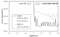
- the secondary harmonic characteristics of the produced nitride semiconductor substrate were evaluated by the same method as in the example. Also, the concentration of Al diffused into the single crystal silicon layer of the growth substrate was measured by the same method as in the example. Results are shown in FIGS.
- each of the single crystal silicon substrates having the following two levels of carbon concentration in the single crystal silicon thin film was used as the donor substrate.
- a nitride semiconductor substrate was fabricated by epitaxially growing a nitride semiconductor thin film in the same manner as in Example except for the above. ⁇ 4E16 atoms/ cm3 ⁇ 1E17 atoms/ cm3
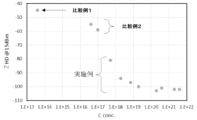
- the carbon concentration of the single-crystal silicon layer, which is the growth surface of the nitride semiconductor thin film is set to 5E17 atoms/cm 3 or more and 1E22 atoms/cm 3 or less, so that the second harmonic characteristics are improved. It's getting better.
- Comparative Example 1 in which the single crystal silicon layer, which is the growth surface of the nitride semiconductor thin film, was not doped with carbon
- Comparative Example 2 in which the carbon concentration of the single crystal silicon layer was less than 5E17 atoms/cm 3 good 2 Order harmonic characteristics are not obtained.
- Al is diffused into the single-crystal silicon layer during the growth of the nitride semiconductor to lower the resistivity, thereby deteriorating the high-frequency characteristics. was found to be able to be suppressed.
- the present invention is not limited to the above embodiments.
- the above-described embodiment is an example, and any device having substantially the same configuration as the technical idea described in the claims of the present invention and exhibiting the same effect is the present invention. included in the technical scope of
Abstract
The present invention is a nitride semiconductor substrate comprising: a growth substrate in which a single crystal silicon layer is formed on a composite substrate obtained by laminating a plurality of layers; and a nitride semiconductor thin film formed on the single crystal silicon layer of the growth substrate, the nitride semiconductor substrate being characterized in that the carbon concentration of the single crystal silicon layer is 5E17 atoms/cm3 to 1E22 atoms/cm3. Consequently, provided are: a nitride semiconductor substrate in which the resistivity becomes low by diffusing Al in a single crystal silicon layer during the growth of a nitride semiconductor, and deterioration in high frequency characteristics is suppressed; and a manufacturing method therefor.
Description
本発明は、窒化物半導体基板及びその製造方法に関する。
The present invention relates to a nitride semiconductor substrate and its manufacturing method.
半導体薄膜製造方法のひとつであるMOCVD法は、大口径化や量産性に優れており、均質な薄膜結晶を成膜できるため、広く用いられている。GaNに代表される窒化物半導体はSi(シリコン)の材料としての限界を超える次世代の半導体材料として期待されている。
The MOCVD method, which is one of the semiconductor thin film manufacturing methods, is widely used because it is excellent in large diameter and mass production, and can form homogeneous thin film crystals. Nitride semiconductors typified by GaN are expected to be next-generation semiconductor materials that surpass the limitations of Si (silicon) as a material.
GaNは飽和電子速度が大きいという特性から高周波動作可能なデバイスの作製が可能であり、また絶縁破壊電界も大きいことから、高出力での動作が可能である。また、軽量化や小型化、低消費電力化も見込める。近年、5G等に代表されるような通信速度の高速化、またそれ伴う高出力化の要求により、高周波、且つ高出力で動作可能なGaN HEMTが注目されている。
GaN has a high saturation electron velocity, making it possible to fabricate devices that can operate at high frequencies, and since it also has a large breakdown electric field, it can operate at high output. In addition, weight reduction, miniaturization, and low power consumption can be expected. In recent years, GaN HEMTs that can operate at high frequencies and high power have been attracting attention due to the demand for higher communication speeds, as typified by 5G, and higher power.
GaNデバイスを作製するためのGaNエピタキシャルウェーハに用いられる基板としては、Si基板が最も安価であり且つ大口径化に有利である。また、熱伝導率が高く放熱性が良いことから、SiC基板も用いられている。しかしこれらの基板は、GaNとの熱膨張係数が異なるため、エピタキシャル成膜後の冷却工程で応力が印加し、クラックが発生しやすい。また強い応力が印加していることで、デバイスプロセス中にウェーハ割れが発生してしまう事がある。また、厚いGaNを成膜する事が不可能であり、エピタキシャル層内に複雑な応力緩和層を成膜してもクラックフリーではせいぜい5μm程度が限界である。
As for the substrates used for GaN epitaxial wafers for producing GaN devices, Si substrates are the cheapest and advantageous for increasing the diameter. SiC substrates are also used because of their high thermal conductivity and good heat dissipation. However, since these substrates have different coefficients of thermal expansion from GaN, stress is applied in the cooling process after the epitaxial film formation, and cracks are likely to occur. In addition, the application of strong stress may cause wafer cracking during the device process. In addition, it is impossible to form a thick GaN film, and even if a complicated stress relaxation layer is formed in the epitaxial layer, the crack-free thickness is at most about 5 μm.
一方、GaN基板はGaNエピタキシャル層と同じ(または非常に近い)熱膨張係数を有する為、上記のような問題は発生しにくいが、自立GaN基板は作製が困難であるだけでなく、極めて高価であり口径の大きい基板が作製できない事から、量産化には不適切である。
On the other hand, since the GaN substrate has the same (or very close to) thermal expansion coefficient as the GaN epitaxial layer, the above-mentioned problems are less likely to occur. It is not suitable for mass production because substrates with large diameters cannot be produced.
そのため、大口径で且つGaNと熱膨張係数が近いGaNエピタキシャル用の大口径基板(以下、GaN用支持基板)が特許文献1に開示されている。このGaN用支持基板は、多結晶セラミックコア、第1の接着層、導電層、第2の接着層、バリア層を含む支持構造と、該支持構造の片面に積層された平坦化層、該平坦化層に積層された単結晶シリコン層により構成される。
Therefore, Patent Document 1 discloses a large-diameter substrate for GaN epitaxial use (hereinafter referred to as a support substrate for GaN) having a large diameter and a coefficient of thermal expansion close to that of GaN. This support substrate for GaN comprises a support structure including a polycrystalline ceramic core, a first adhesion layer, a conductive layer, a second adhesion layer, and a barrier layer; It is composed of a single crystal silicon layer laminated on a silicon layer.
この成長用支持基板を用いることで、大口径で且つエピタキシャル層の厚さが厚く、且つクラックの発生しない窒化物半導体基板を作製できる。また、GaNと熱膨張係数差が極めて小さい事から、GaN成長中や冷却中に反りが発生しにくいため、成膜後の基板の反りを小さく制御できるだけでなく、エピタキシャル層中に複雑な応力緩和層を設ける必要が無いため、エピタキシャル成膜時間が短くなり、エピタキシャル成長のコストを大幅に削減できる。さらに、成長用支持基板は大部分がセラミックスであるため、基板自体が非常に硬く塑性変形しにくいだけでなく、口径の大きいGaN on Siで解決されていないウェーハ割れが発生しない。
By using this growth supporting substrate, a nitride semiconductor substrate having a large diameter, a thick epitaxial layer, and no cracks can be produced. In addition, since the difference in thermal expansion coefficient from GaN is extremely small, warping is less likely to occur during GaN growth and cooling. Since there is no need to provide a layer, the epitaxial film formation time is shortened, and the cost of epitaxial growth can be greatly reduced. Furthermore, since most of the growth support substrate is made of ceramics, the substrate itself is very hard and resistant to plastic deformation.
高周波用途で用いられるGaN on Siデバイスでは、高抵抗の単結晶シリコン基板が用いられる。しかし、単結晶シリコン基板上にAlN、AlGaN、GaN等を成膜する過程で、AlとGaが単結晶シリコン基板中に拡散し、単結晶シリコン基板表層(窒化物半導体エピタキシャル層との界面付近)が低抵抗化してしまい、高周波特性が劣化するという問題がある。
GaN on Si devices used for high-frequency applications use high-resistance single-crystal silicon substrates. However, in the process of forming films of AlN, AlGaN, GaN, etc. on the single crystal silicon substrate, Al and Ga diffuse into the single crystal silicon substrate, and the surface layer of the single crystal silicon substrate (near the interface with the nitride semiconductor epitaxial layer) has a low resistance, resulting in deterioration of high-frequency characteristics.
GaN用支持基板の表層も単結晶シリコン層であるため、高周波用途で使用される際、AlN、AlGaN、GaN等の成長中に単結晶シリコン層内にAlとGaが拡散され、同様の高周波損失の問題が発生する。
Since the surface layer of the GaN support substrate is also a single-crystal silicon layer, when used for high-frequency applications, Al and Ga are diffused into the single-crystal silicon layer during the growth of AlN, AlGaN, GaN, etc., resulting in similar high-frequency loss. problem occurs.
本発明は上記課題を解決するためになされたもので、窒化物半導体の成長中に単結晶シリコン層内にAlが拡散され低抵抗率化されて、高周波特性が劣化することを抑制した窒化物半導体基板及びその製造方法を提供することを目的とする。
The present invention has been made to solve the above problems, and is a nitride semiconductor in which Al is diffused into a single-crystal silicon layer during the growth of the nitride semiconductor to lower the resistivity, thereby suppressing deterioration of high-frequency characteristics. An object of the present invention is to provide a semiconductor substrate and a method for manufacturing the same.
上記課題を解決するために、本発明では、
複数の層が積層された複合基板上に単結晶シリコン層が形成された成長用基板と、該成長用基板の前記単結晶シリコン層上に成膜された窒化物半導体薄膜とを具備する窒化物半導体基板であって、
前記単結晶シリコン層の炭素濃度が、5E17atoms/cm3以上、1E22atoms/cm3以下のものである窒化物半導体基板を提供する。 In order to solve the above problems, in the present invention,
A nitride comprising a growth substrate in which a single crystal silicon layer is formed on a composite substrate in which a plurality of layers are laminated, and a nitride semiconductor thin film formed on the single crystal silicon layer of the growth substrate A semiconductor substrate,
A nitride semiconductor substrate is provided, wherein the single crystal silicon layer has a carbon concentration of 5E17 atoms/cm 3 or more and 1E22 atoms/cm 3 or less.
このように単結晶シリコン層の炭素濃度が5E17atoms/cm3以上であれば、単結晶シリコン層内へのAlとGaの拡散を抑制し、単結晶シリコン層の低抵抗化を抑制する事ができる。また、単結晶シリコン層の炭素濃度が1E22atoms/cm3以下であれば、結晶性の悪化を防ぐことができるため結晶性のよい基板とすることができる。その結果、高周波特性の良い窒化物半導体基板を提供する事ができる。
Thus, if the carbon concentration of the single crystal silicon layer is 5E17 atoms/cm 3 or more, the diffusion of Al and Ga into the single crystal silicon layer can be suppressed, and the resistance of the single crystal silicon layer can be suppressed from decreasing. . Further, when the carbon concentration of the single crystal silicon layer is 1E22 atoms/cm 3 or less, deterioration of crystallinity can be prevented, so that the substrate can have good crystallinity. As a result, it is possible to provide a nitride semiconductor substrate with good high frequency characteristics.
また、前記窒化物半導体薄膜は、GaN、AlN、及びAlGaNのうち1つ以上を含むものであることが好ましい。
Also, the nitride semiconductor thin film preferably contains one or more of GaN, AlN, and AlGaN.
このような窒化物半導体薄膜であれば、確実に高周波特性の良い窒化物半導体基板を提供する事ができる。
With such a nitride semiconductor thin film, it is possible to reliably provide a nitride semiconductor substrate with good high-frequency characteristics.
また、前記単結晶シリコン層は100~500nmの厚さを有し、前記窒化物半導体薄膜の総膜厚は2μm以上10μm以下であることが好ましい。
Further, it is preferable that the single crystal silicon layer has a thickness of 100 to 500 nm, and the total thickness of the nitride semiconductor thin film is 2 μm or more and 10 μm or less.
本発明では、単結晶シリコン層及び窒化物半導体薄膜をこのような厚さとすることができる。
In the present invention, the single crystal silicon layer and the nitride semiconductor thin film can have such thicknesses.
また、前記複合基板は、多結晶セラミックコアと、該多結晶セラミックコア全体に積層された第1の接着層と、該第1の接着層全体に積層された第2の接着層と、該第2の接着層全体に積層されたバリア層とを含むものであり、かつ、
前記単結晶シリコン層は、前記複合基板の片面のみに積層された平坦化層の上に形成されたものであることが好ましい。 The composite substrate includes a polycrystalline ceramic core, a first adhesive layer laminated over the entire polycrystalline ceramic core, a second adhesive layer laminated over the first adhesive layer, and the second adhesive layer laminated over the entire first adhesive layer. a barrier layer laminated over the adhesive layer of 2, and
It is preferable that the single-crystal silicon layer is formed on a planarization layer laminated only on one side of the composite substrate.
このような構成であれば、成長用基板の大部分がセラミックスであるため、基板自体が非常に硬く塑性変形しにくいだけでなく、シリコン基板で解決されていないウェーハ割れも発生しない。
With this structure, most of the growth substrate is made of ceramics, so not only is the substrate itself extremely hard and resistant to plastic deformation, but wafer cracking, which has not been resolved with silicon substrates, does not occur.
また、前記複合基板が、前記第1の接着層と前記第2の接着層との間に、前記第1の接着層全体に積層された導電層を有するものであってもよい。
Further, the composite substrate may have, between the first adhesive layer and the second adhesive layer, a conductive layer laminated over the entire first adhesive layer.
複合基板には、必要に応じて導電性を付与することができる。
The composite substrate can be given conductivity as needed.
また、前記複合基板は、多結晶セラミックコアと、該多結晶セラミックコア全体に積層された第1の接着層と、該第1の接着層全体に積層されたバリア層と、該バリア層の裏面に積層された第2の接着層と、該第2の接着層の裏面に積層された導電層とを含むものであり、かつ、
前記単結晶シリコン層は、前記複合基板の前記バリア層の表面に積層された平坦化層の上に形成されたものであることが好ましい。 The composite substrate includes a polycrystalline ceramic core, a first adhesive layer laminated on the entire polycrystalline ceramic core, a barrier layer laminated on the entire first adhesive layer, and a rear surface of the barrier layer. and a conductive layer laminated to the back surface of the second adhesive layer, and
Preferably, the single-crystal silicon layer is formed on a planarization layer laminated on the surface of the barrier layer of the composite substrate.
このような成長用基板を用いた窒化物半導体基板であれば、成長用基板の表面側導電層によるリークパスが生じず、高周波特性に優れたものとすることができる。
A nitride semiconductor substrate using such a growth substrate does not generate a leak path due to the surface-side conductive layer of the growth substrate, and can have excellent high-frequency characteristics.
また、前記複合基板は、多結晶セラミックコアと、該多結晶セラミックコア全体に積層された第1の接着層と、該第1の接着層の裏面に積層された導電層と、該導電層の裏面に積層された第2の接着層と、前記第1の接着層の表面及び側面と前記導電層の側面と前記第2の接着層の側面及び裏面に積層されたバリア層とを含むものであり、かつ、
前記単結晶シリコン層は、前記複合基板の前記バリア層の表面に積層された平坦化層の上に形成されたものであることが好ましい。 The composite substrate includes a polycrystalline ceramic core, a first adhesive layer laminated over the entire polycrystalline ceramic core, a conductive layer laminated on the back surface of the first adhesive layer, and the conductive layer. A second adhesive layer laminated on the back surface, a barrier layer laminated on the front and side surfaces of the first adhesive layer, the side surface of the conductive layer, and the side surfaces and the back surface of the second adhesive layer. Yes, and
Preferably, the single-crystal silicon layer is formed on a planarization layer laminated on the surface of the barrier layer of the composite substrate.
このような成長用基板を用いた窒化物半導体基板であっても、成長用基板の表面側導電層によるリークパスが生じず、高周波特性に優れたものとすることができる。
Even with a nitride semiconductor substrate using such a growth substrate, it is possible to achieve excellent high-frequency characteristics without causing a leak path due to the surface-side conductive layer of the growth substrate.
このとき、前記導電層が、ポリシリコン層を含むものであることが好ましい。
At this time, the conductive layer preferably includes a polysilicon layer.
導電層は、このような層とすることができる。
The conductive layer can be such a layer.
このとき、前記多結晶セラミックコアが、窒化アルミニウムを含むものであることが好ましい。
At this time, the polycrystalline ceramic core preferably contains aluminum nitride.
このような複合基板とすれば、窒化物半導体との熱膨張係数差を極めて小さくできる。
With such a composite substrate, the difference in thermal expansion coefficient from the nitride semiconductor can be made extremely small.
また、前記第1の接着層及び前記第2の接着層はテトラエチルオルトシリケート(TEOS)層又は酸化シリコン(SiO2)層を含み、前記バリア層は窒化シリコンを含むものであることが好ましい。
Also, it is preferable that the first adhesive layer and the second adhesive layer include a tetraethylorthosilicate (TEOS) layer or a silicon oxide (SiO 2 ) layer, and the barrier layer includes silicon nitride.
第1の接着層及び第2の接着層、及びバリア層は、このような層とすることができる。
The first adhesive layer, the second adhesive layer, and the barrier layer can be such layers.
また、前記平坦化層はテトラエチルオルトシリケート(TEOS)又は酸化シリコン(SiO2)を含み、かつ、500~3000nmの厚さを有するものであることが好ましい。
Also, the planarization layer preferably contains tetraethylorthosilicate (TEOS) or silicon oxide (SiO 2 ) and has a thickness of 500 to 3000 nm.
平坦化層は、このような層とすることができる。
The planarization layer can be such a layer.
また本発明では、成長用基板と、該成長用基板上に成膜された窒化物半導体薄膜とを具備する窒化物半導体基板の製造方法であって、
(1)複数の層が積層された複合基板上に、炭素濃度が5E17atoms/cm3以上、1E22atoms/cm3以下の単結晶シリコン層を形成して、成長用基板を作製する工程、及び
(2)前記成長用基板の前記単結晶シリコン層上に前記窒化物半導体薄膜をエピタキシャル成長させて、窒化物半導体基板を製造する工程
を含む窒化物半導体基板の製造方法を提供する。 Further, according to the present invention, there is provided a method for manufacturing a nitride semiconductor substrate comprising a growth substrate and a nitride semiconductor thin film formed on the growth substrate, comprising:
(1) forming a single crystal silicon layer having a carbon concentration of 5E17 atoms/cm 3 or more and 1E22 atoms/cm 3 or less on a composite substrate in which a plurality of layers are laminated to prepare a growth substrate; ) A method for manufacturing a nitride semiconductor substrate, comprising the step of epitaxially growing the nitride semiconductor thin film on the single crystal silicon layer of the growth substrate to manufacture the nitride semiconductor substrate.
このように単結晶シリコン層の炭素濃度が5E17atoms/cm3以上1E22atoms/cm3以下の成長用基板を用いた窒化物半導体基板の製造方法であれば、比較的容易に高周波特性の良い窒化物半導体基板を製造することができる。
As described above, if a method for manufacturing a nitride semiconductor substrate using a growth substrate having a single crystal silicon layer with a carbon concentration of 5E17 atoms/cm 3 or more and 1E22 atoms/cm 3 or less is used, a nitride semiconductor having good high frequency characteristics can be produced relatively easily. A substrate can be manufactured.
また、前記工程(1)を、
(1-1)前記複合基板として、多結晶セラミックコアと、該多結晶セラミックコア全体に積層された第1の接着層と、該第1の接着層全体に積層された第2の接着層と、該第2の接着層全体に積層されたバリア層とを含む複合基板を準備する工程、
(1-2)前記複合基板の片面のみに平坦化層を積層する工程、及び
(1-3)前記平坦化層に、100~500nmの厚さを有し、かつ、5E17atoms/cm3以上、1E22atoms/cm3以下の濃度で炭素ドープされた単結晶シリコン層を備えるドナー基板を貼り合わせることにより、前記単結晶シリコン層を形成する工程
を含む工程とすることが好ましい。 Further, the step (1) is
(1-1) The composite substrate includes a polycrystalline ceramic core, a first adhesive layer laminated over the polycrystalline ceramic core, and a second adhesive layer laminated over the first adhesive layer. and a barrier layer laminated over the second adhesive layer;
(1-2) a step of laminating a planarization layer only on one side of the composite substrate; and (1-3) the planarization layer has a thickness of 100 to 500 nm and is 5E17 atoms/cm 3 or more; The step preferably includes a step of forming a single crystal silicon layer by bonding a donor substrate having a single crystal silicon layer doped with carbon at a concentration of 1E22 atoms/cm 3 or less.
このようにすれば、成長用基板の大部分がセラミックスであるため、基板自体が非常に硬く塑性変形しにくいだけでなく、シリコン基板で解決されていないウェーハ割れも発生しない窒化物半導体基板を確実に製造することができる。
In this way, since most of the substrate for growth is made of ceramics, the substrate itself is very hard and resistant to plastic deformation. can be manufactured to
このとき、前記工程(1-1)において、前記複合基板を、前記第1の接着層と前記第2の接着層との間に、前記第1の接着層全体に積層された導電層を有するものとすることができる。
At this time, in the step (1-1), the composite substrate has a conductive layer laminated on the entire first adhesive layer between the first adhesive layer and the second adhesive layer. can be
複合基板には、必要に応じて導電性を付与することができる。
The composite substrate can be given conductivity as needed.
また、前記工程(1)を、
(1-1)前記複合基板として、多結晶セラミックコアと、該多結晶セラミックコア全体に積層された第1の接着層と、該第1の接着層全体に積層されたバリア層と、該バリア層の裏面に積層された第2の接着層と、該第2の接着層の裏面に積層された導電層とを含む複合基板を準備する工程、
(1-2)前記複合基板の前記バリア層の表面に平坦化層を積層する工程、及び
(1-3)前記平坦化層に、100~500nmの厚さを有し、かつ、5E17atoms/cm3以上、1E22atoms/cm3以下の濃度で炭素ドープされた単結晶シリコン層を備えるドナー基板を貼り合わせることにより、前記単結晶シリコン層を形成する工程
を含む工程とすることが好ましい。 Further, the step (1) is
(1-1) As the composite substrate, a polycrystalline ceramic core, a first adhesive layer laminated over the entire polycrystalline ceramic core, a barrier layer laminated over the entire first adhesive layer, and the barrier providing a composite substrate comprising a second adhesive layer laminated to the backside of a layer and a conductive layer laminated to the backside of the second adhesive layer;
(1-2) a step of laminating a planarization layer on the surface of the barrier layer of the composite substrate; and (1-3) the planarization layer has a thickness of 100 to 500 nm and 5E17 atoms/cm The step preferably includes a step of forming a single crystal silicon layer by bonding a donor substrate having a single crystal silicon layer doped with carbon at a concentration of 3 or more and 1E22 atoms/cm 3 or less.
このような窒化物半導体基板の製造方法であれば、複合基板の表面側導電層によるリークパスが生じず、高周波特性に優れた窒化物半導体基板を製造することができる。
With such a method for manufacturing a nitride semiconductor substrate, it is possible to manufacture a nitride semiconductor substrate excellent in high-frequency characteristics without causing a leak path due to the surface-side conductive layer of the composite substrate.
また、前記工程(1)を、
(1-1)前記複合基板として、多結晶セラミックコアと、該多結晶セラミックコア全体に積層された第1の接着層と、該第1の接着層の裏面に積層された導電層と、該導電層の裏面に積層された第2の接着層と、前記第1の接着層の表面及び側面と前記導電層の側面と前記第2の接着層の側面及び裏面に積層されたバリア層とを含む複合基板を準備する工程、
(1-2)前記複合基板の前記バリア層の表面に平坦化層を積層する工程、及び
(1-3)前記平坦化層に、100~500nmの厚さを有し、かつ、5E17atoms/cm3以上、1E22atoms/cm3以下の濃度で炭素ドープされた単結晶シリコン層を備えるドナー基板を貼り合わせることにより、前記単結晶シリコン層を形成する工程
を含む工程とすることが好ましい。 Further, the step (1) is
(1-1) As the composite substrate, a polycrystalline ceramic core, a first adhesive layer laminated over the entire polycrystalline ceramic core, a conductive layer laminated on the rear surface of the first adhesive layer, and the A second adhesive layer laminated on the back surface of the conductive layer, a barrier layer laminated on the front and side surfaces of the first adhesive layer, the side surfaces of the conductive layer, and the side and back surfaces of the second adhesive layer. preparing a composite substrate comprising;
(1-2) a step of laminating a planarization layer on the surface of the barrier layer of the composite substrate; and (1-3) the planarization layer has a thickness of 100 to 500 nm and 5E17 atoms/cm The step preferably includes a step of forming a single crystal silicon layer by bonding a donor substrate having a single crystal silicon layer doped with carbon at a concentration of 3 or more and 1E22 atoms/cm 3 or less.
このような窒化物半導体基板の製造方法であっても、複合基板の表面側導電層によるリークパスが生じず、高周波特性に優れた窒化物半導体基板を製造することができる。
Even with such a method for manufacturing a nitride semiconductor substrate, it is possible to manufacture a nitride semiconductor substrate excellent in high-frequency characteristics without causing a leak path due to the surface-side conductive layer of the composite substrate.
また、前記工程(1-3)を、
(1-3-1)単結晶シリコン基板上に前記炭素ドープされた単結晶シリコン薄膜をCVD法によって成膜し、前記ドナー基板を作製する工程、
(1-3-2)前記ドナー基板の前記炭素ドープされた単結晶シリコン薄膜を、前記平坦化層と貼り合わせる工程、及び
(1-3-3)前記ドナー基板の前記単結晶シリコン基板を除去し、さらに、前記ドナー基板の前記炭素ドープされた単結晶シリコン薄膜を所望の厚みとなるように加工して、前記炭素濃度が5E17atoms/cm3以上、1E22atoms/cm3以下の単結晶シリコン層を形成する工程
を含む工程とすることが好ましい。 Further, the step (1-3),
(1-3-1) forming the carbon-doped single crystal silicon thin film on a single crystal silicon substrate by a CVD method to prepare the donor substrate;
(1-3-2) bonding the carbon-doped single crystal silicon thin film of the donor substrate to the planarizing layer; and (1-3-3) removing the single crystal silicon substrate of the donor substrate. Further, the carbon-doped single crystal silicon thin film of the donor substrate is processed to have a desired thickness to form a single crystal silicon layer having a carbon concentration of 5E17 atoms/cm 3 or more and 1E22 atoms/cm 3 or less. It is preferable that the process includes a forming process.
このようにすれば、比較的簡単に確実に高炭素濃度の単結晶シリコン薄膜を有するドナー基板を製造することができるだけでなく、平坦化層上に所望の厚みの単結晶シリコン層を容易に形成することができる。
By doing so, not only can a donor substrate having a single-crystal silicon thin film with a high carbon concentration be relatively easily and reliably manufactured, but also a single-crystal silicon layer having a desired thickness can be easily formed on the planarizing layer. can do.
以上のように、本発明であれば、窒化物半導体の成長中に単結晶シリコン層内にAlとGaが拡散され低抵抗率化されて、高周波特性が劣化することを抑制した窒化物半導体基板及びその製造方法を提供することができる。
As described above, according to the present invention, Al and Ga are diffused into the single-crystal silicon layer during the growth of the nitride semiconductor to lower the resistivity, thereby suppressing the deterioration of the high-frequency characteristics of the nitride semiconductor substrate. and a method for producing the same.
上述したように、単結晶シリコン層上に窒化物半導体を成膜する過程で、AlとGaが単結晶シリコン層中に拡散し、単結晶シリコン層の表層(GaNエピタキシャル層との界面付近)が低抵抗率化してしまい、高周波特性が劣化するという問題がある。
As described above, in the process of forming a nitride semiconductor film on the single-crystal silicon layer, Al and Ga diffuse into the single-crystal silicon layer, and the surface layer of the single-crystal silicon layer (near the interface with the GaN epitaxial layer) becomes There is a problem that the resistivity is lowered and the high frequency characteristics are degraded.
本発明者らは、GaN成長中に単結晶シリコン層内にAlとGaが拡散して低抵抗率化して、高周波特性が劣化することを抑制する方法について検討を重ねたところ、単結晶シリコン層の炭素濃度を5E17atoms/cm3以上、1E22atoms/cm3以下とすることで、単結晶シリコン層内へのAlとGaの拡散を抑制し、単結晶シリコン層の低抵抗化を抑制する事ができ、結晶性の良い基板と炭素による拡散バリアを両立させることで、高周波特性の良い窒化物半導体基板とすることができることが判り、本発明を完成させた。
The inventors of the present invention conducted repeated studies on a method for suppressing the deterioration of high-frequency characteristics due to the diffusion of Al and Ga into the single crystal silicon layer during the growth of GaN, resulting in a low resistivity. With the carbon concentration of 5E17 atoms/cm 3 or more and 1E22 atoms/cm 3 or less, the diffusion of Al and Ga into the single crystal silicon layer can be suppressed, and the resistance of the single crystal silicon layer can be suppressed from decreasing. It was found that a nitride semiconductor substrate having good high-frequency characteristics can be obtained by combining a substrate with good crystallinity and a carbon diffusion barrier, and the present invention has been completed.
即ち、本発明は、複数の層が積層された複合基板上に単結晶シリコン層が形成された成長用基板と、該成長用基板の前記単結晶シリコン層上に成膜された窒化物半導体薄膜とを具備する窒化物半導体基板であって、前記単結晶シリコン層の炭素濃度が、5E17atoms/cm3以上、1E22atoms/cm3以下のものである窒化物半導体基板である。
That is, the present invention provides a growth substrate in which a single crystal silicon layer is formed on a composite substrate in which a plurality of layers are laminated, and a nitride semiconductor thin film formed on the single crystal silicon layer of the growth substrate. wherein the single crystal silicon layer has a carbon concentration of 5E17 atoms/cm 3 or more and 1E22 atoms/cm 3 or less.
また本発明は、成長用基板と、該成長用基板上に成膜された窒化物半導体薄膜とを具備する窒化物半導体基板の製造方法であって、(1)複数の層が積層された複合基板上に、炭素濃度が5E17atoms/cm3以上、1E22atoms/cm3以下の単結晶シリコン層を形成して、成長用基板を作製する工程、及び(2)前記成長用基板の前記単結晶シリコン層上に前記窒化物半導体薄膜をエピタキシャル成長させて、窒化物半導体基板を製造する工程を含む窒化物半導体基板の製造方法である。
The present invention also provides a method for manufacturing a nitride semiconductor substrate comprising a growth substrate and a nitride semiconductor thin film formed on the growth substrate, comprising: (1) a composite in which a plurality of layers are laminated; forming a single crystal silicon layer having a carbon concentration of 5E17 atoms/cm 3 or more and 1E22 atoms/cm 3 or less on a substrate to fabricate a growth substrate; and (2) the single crystal silicon layer of the growth substrate. A method for manufacturing a nitride semiconductor substrate, comprising the step of epitaxially growing the nitride semiconductor thin film thereon to manufacture a nitride semiconductor substrate.
以下、本発明について詳細に説明するが、本発明はこれらに限定されるものではない。
Although the present invention will be described in detail below, the present invention is not limited to these.
[窒化物半導体基板]
本発明の窒化物半導体基板は、例えば、図1に示すような複数の層が積層された複合基板200上に単結晶シリコン層7が形成された成長用基板100と、該成長用基板100の前記単結晶シリコン層7上に成膜された窒化物半導体薄膜8とを具備する窒化物半導体基板300であって、前記単結晶シリコン層7の炭素濃度が、5E17atoms/cm3以上、1E22atoms/cm3以下のものである。 [Nitride semiconductor substrate]
The nitride semiconductor substrate of the present invention includes, for example, agrowth substrate 100 in which a single crystal silicon layer 7 is formed on a composite substrate 200 in which a plurality of layers are laminated as shown in FIG. and a nitride semiconductor thin film 8 formed on the single crystal silicon layer 7, wherein the carbon concentration of the single crystal silicon layer 7 is 5E17 atoms/cm 3 or more and 1E22 atoms/cm 3 or less.
本発明の窒化物半導体基板は、例えば、図1に示すような複数の層が積層された複合基板200上に単結晶シリコン層7が形成された成長用基板100と、該成長用基板100の前記単結晶シリコン層7上に成膜された窒化物半導体薄膜8とを具備する窒化物半導体基板300であって、前記単結晶シリコン層7の炭素濃度が、5E17atoms/cm3以上、1E22atoms/cm3以下のものである。 [Nitride semiconductor substrate]
The nitride semiconductor substrate of the present invention includes, for example, a
このように単結晶シリコン層7の炭素濃度が5E17atoms/cm3以上であれば、単結晶シリコン層7内へのAlとGaの拡散を抑制し、単結晶シリコン層7の低抵抗化を抑制する事ができる。また、単結晶シリコン層7の炭素濃度が1E22atoms/cm3以下であれば、結晶性の悪化を防ぐことができるため結晶性のよい基板とすることができる。その結果、高周波特性の良い窒化物半導体基板を提供する事ができる。
Thus, if the carbon concentration of the single-crystal silicon layer 7 is 5E17 atoms/cm 3 or more, the diffusion of Al and Ga into the single-crystal silicon layer 7 is suppressed, and the resistance of the single-crystal silicon layer 7 is suppressed. can do things Further, if the carbon concentration of the single-crystal silicon layer 7 is 1E22 atoms/cm 3 or less, deterioration of crystallinity can be prevented, and a substrate with good crystallinity can be obtained. As a result, it is possible to provide a nitride semiconductor substrate with good high frequency characteristics.
また、より優れた二次高調波特性を得る観点から、単結晶シリコン層7の炭素濃度は1E18atoms/cm3以上とすることが好ましい。
From the viewpoint of obtaining better second harmonic characteristics, the carbon concentration of the single crystal silicon layer 7 is preferably 1E18 atoms/cm 3 or more.
成長用基板
図1に示すように、成長用基板100は、例えば多結晶セラミックコア1と、該多結晶セラミックコア1全体に積層された第1の接着層2と、該第1の接着層2全体に積層された導電層3と、該導電層3全体に積層された第2の接着層4と、該第2の接着層4全体に積層されたバリア層5とを含む複合基板200(支持構造)と、該複合基板200の片面のみに積層された平坦化層6と、該平坦化層6に積層された上記炭素濃度の単結晶シリコン層7(実質的単結晶シリコン層)により構成される。尚、上記導電層3および第1の接着層2は必要に応じて成膜されるものであり、必ずしも存在するわけではなく、また片面のみに成膜されている場合もある。 Substrate for growth As shown in FIG. A composite substrate 200 (support structure), aplanarization layer 6 laminated only on one side of the composite substrate 200, and a single crystal silicon layer 7 (substantially single crystal silicon layer) having the above carbon concentration laminated on the planarization layer 6. be. Incidentally, the conductive layer 3 and the first adhesive layer 2 are formed as necessary, and are not necessarily present, and may be formed only on one side.
図1に示すように、成長用基板100は、例えば多結晶セラミックコア1と、該多結晶セラミックコア1全体に積層された第1の接着層2と、該第1の接着層2全体に積層された導電層3と、該導電層3全体に積層された第2の接着層4と、該第2の接着層4全体に積層されたバリア層5とを含む複合基板200(支持構造)と、該複合基板200の片面のみに積層された平坦化層6と、該平坦化層6に積層された上記炭素濃度の単結晶シリコン層7(実質的単結晶シリコン層)により構成される。尚、上記導電層3および第1の接着層2は必要に応じて成膜されるものであり、必ずしも存在するわけではなく、また片面のみに成膜されている場合もある。 Substrate for growth As shown in FIG. A composite substrate 200 (support structure), a
ここで、多結晶セラミックコア1は窒化アルミニウムを含み、焼結助剤によって例えば1800度の高温で焼結され、約600~1150μmの厚さを有する。基本的にはシリコン基板のSEMI規格の厚さで形成される場合が多い。
Here, the polycrystalline ceramic core 1 contains aluminum nitride, is sintered at a high temperature of, for example, 1800 degrees with a sintering aid, and has a thickness of about 600-1150 μm. Basically, it is often formed with a thickness of the SEMI standard for the silicon substrate.
第1の接着層2および第2の接着層4は、テトラエチルオルトシリケート(TEOS)層ないしは酸化シリコン(SiO2)層、またはその両方を含む層で、LPCVDプロセスやCVDプロセス等によって堆積され、おおよそ50~200nmの厚さを有する。
The first adhesion layer 2 and the second adhesion layer 4 are layers including a tetraethylorthosilicate (TEOS) layer, a silicon oxide ( SiO2 ) layer, or both, and are deposited by an LPCVD process, a CVD process, or the like. It has a thickness of 50-200 nm.
導電層3は、ポリシリコンを含み、LPCVDプロセス等によって堆積され、約150~500nmの厚さを有する。これは導電性を付与するための層であり、例えばホウ素(B)やリン(P)等がドープされる。このポリシリコンを含む導電層3は、必要に応じて設けるものであって、なくても良く、また片面のみに成膜されていても良い。
The conductive layer 3 contains polysilicon, is deposited by an LPCVD process or the like, and has a thickness of about 150-500 nm. This is a layer for imparting electrical conductivity, and is doped with, for example, boron (B) or phosphorus (P). The conductive layer 3 containing polysilicon is provided as required, and may be omitted or may be formed only on one side.
また、バリア層5は、窒化シリコン層を含み、LPCVDプロセス等によって堆積され、例えば、100~1000nmの厚さを有する。
Also, the barrier layer 5 includes a silicon nitride layer, is deposited by an LPCVD process or the like, and has a thickness of, for example, 100-1000 nm.
平坦化層6は、LPCVDプロセス等によって堆積され、厚さは500~3000nm程度である。この平坦化層6は上面の平坦化のために堆積され、好ましくはテトラエチルオルトシリケート(TEOS)又は酸化シリコン(SiO2)を含むものであるが、SiO2、Al2O3、Si3N4、あるいは酸窒化シリコン(SixOyNz)等の通常のセラミックスの膜材等であってもよい。
The planarization layer 6 is deposited by an LPCVD process or the like, and has a thickness of approximately 500 to 3000 nm. This planarization layer 6 is deposited for planarization of the top surface and preferably comprises tetraethylorthosilicate (TEOS) or silicon oxide ( SiO2 ), but also SiO2 , Al2O3 , Si3N4 , or Ordinary ceramic film materials such as silicon oxynitride (Si x O y N z ) may be used.
単結晶シリコン層7は、例えば、約100~500nmの厚さを有し、GaNなどの他のエピタキシャル成長のための成長面として利用される層であり、層転写プロセス等を用いて平坦化層6に接合される。上述のとおり、単結晶シリコン層7は所定濃度の炭素がドープされたものである。
The single crystal silicon layer 7 has a thickness of, for example, about 100 to 500 nm and is a layer used as a growth surface for epitaxial growth of other materials such as GaN. is spliced to As described above, the monocrystalline silicon layer 7 is doped with carbon at a predetermined concentration.
尚、各層の厚さや製造方法、用いられる物質等は、上記のものに限定されず、必ずしも全ての層が存在する必要もない。
It should be noted that the thickness of each layer, the manufacturing method, the materials used, etc. are not limited to those described above, and all layers do not necessarily need to be present.
また、前記成長用基板の別の例としては、例えば図4に示すように多結晶セラミックコア1と、前記多結晶セラミックコアに全体に結合された第1の接着層2と、前記第1の接着層全体に結合されたバリア層5と、前記バリア層の裏面に結合された第2の接着層4と、前記第2の接着層の裏面に結合された導電層3とを含む複合基板と、前記複合基板の表面のみに結合された平坦化層6と、前記平坦化層に結合された単結晶シリコン層7により構成されることができる。
As another example of the substrate for growth, as shown in FIG. A composite substrate comprising a barrier layer 5 bonded over the adhesive layer, a second adhesive layer 4 bonded to the back surface of said barrier layer, and a conductive layer 3 bonded to the back surface of said second adhesive layer. , a planarization layer 6 bonded only to the surface of said composite substrate, and a monocrystalline silicon layer 7 bonded to said planarization layer.
このような導電層3が裏面側にだけに成膜されている構造の成長用基板を用いた窒化物半導体基板であれば、高周波デバイスを作製する場合に成長用基板の表面側導電層によるリークパスが生じず、高周波特性に優れたものとすることができる。
In the case of a nitride semiconductor substrate using a growth substrate having such a structure in which the conductive layer 3 is formed only on the rear surface side, a leak path due to the front surface side conductive layer of the growth substrate is required when fabricating a high-frequency device. does not occur, and excellent high-frequency characteristics can be obtained.
また、前記成長用基板のさらに別の例としては、例えば図5に示すように多結晶セラミックコア1と、前記多結晶セラミックコアに全体に結合された第1の接着層2と、前記第1の接着層の裏面に結合された導電層3と、前記導電層の裏面に結合された第2の接着層4と、前記第1の接着層の表面及び側面と前記導電層の側面と前記第2の接着層の側面及び裏面に結合されたバリア層5とを含む複合基板と、前記複合基板の表面のみに結合された平坦化層6と、前記平坦化層に結合された単結晶シリコン層7により構成されることができる。
Further, as another example of the growth substrate, for example, as shown in FIG. a conductive layer 3 bonded to the back surface of the adhesive layer of the second adhesive layer 4 bonded to the back surface of the conductive layer; the front and side surfaces of the first adhesive layer; the side surfaces of the conductive layer; 2, a planarization layer 6 bonded only to the surface of said composite substrate, and a monocrystalline silicon layer bonded to said planarization layer. 7.
このような導電層3が裏面側にだけに成膜されている構造の成長用基板を用いた窒化物半導体基板であっても、高周波デバイスを作製する場合に成長用基板の表面側導電層によるリークパスが生じず、高周波特性に優れたものとすることができる。
Even in a nitride semiconductor substrate using a growth substrate having such a structure in which the conductive layer 3 is formed only on the back surface side, when a high-frequency device is manufactured, the front surface side conductive layer of the growth substrate is used. A leak path does not occur, and excellent high-frequency characteristics can be obtained.
窒化物半導体薄膜
成長用基板100の単結晶シリコン層7の上に形成する窒化物半導体薄膜8としては特に限定されないが、例えば、GaN、AlN、及びAlGaNのうち1つ以上を含むものとすることができる。 The nitride semiconductorthin film 8 formed on the single crystal silicon layer 7 of the nitride semiconductor thin film growth substrate 100 is not particularly limited, but may contain, for example, one or more of GaN, AlN, and AlGaN. .
成長用基板100の単結晶シリコン層7の上に形成する窒化物半導体薄膜8としては特に限定されないが、例えば、GaN、AlN、及びAlGaNのうち1つ以上を含むものとすることができる。 The nitride semiconductor
すなわち窒化物半導体薄膜は、AlN、AlGaNおよびGaN等のエピタキシャル成長層とすることができるが、エピタキシャル層の構造はこれに限らず、AlGaNを成膜しない場合や、AlGaN成膜後さらにAlNを成膜する場合もある。また、Al組成を変化させたAlGaNを複数層成膜させる場合もある。
That is, the nitride semiconductor thin film can be an epitaxially grown layer of AlN, AlGaN, GaN, or the like, but the structure of the epitaxial layer is not limited to this. sometimes. In some cases, multiple layers of AlGaN with different Al compositions are deposited.
エピタキシャル層の表層側にはデバイス層を設けることができる。デバイス層は、2次元電子ガスが発生する結晶性の高い層(チャネル層)、2次元電子ガスを発生させるための層(バリア層)、最表層にcap層を設けた構造とすることができる。チャネル層は例えばGaN層とすることができるが、これに限定されない。バリア層はAl組成が20%程度のAlGaNを用いることができるが、例えばInGaN等も用いることができ、これに限定されない。Cap層は例えばGaN層やSiN層とすることもでき、これに限定されない。また、これらのデバイス層の厚さやバリア層のAl組成は、デバイスの設計によって変更することができる。
A device layer can be provided on the surface layer side of the epitaxial layer. The device layer can have a structure comprising a highly crystalline layer (channel layer) for generating a two-dimensional electron gas, a layer (barrier layer) for generating a two-dimensional electron gas, and a cap layer as the outermost layer. . The channel layer can be, for example, a GaN layer, but is not limited to this. AlGaN with an Al composition of about 20% can be used for the barrier layer, but, for example, InGaN or the like can also be used, and the material is not limited to this. The Cap layer can be, for example, a GaN layer or a SiN layer, but is not limited to this. Also, the thickness of these device layers and the Al composition of the barrier layer can be changed according to the design of the device.
窒化物半導体薄膜の膜厚は用途によって変更されるため、特に限定されないが、窒化物半導体薄膜の総膜厚は2μm以上10μm以下であることが好ましい。
The thickness of the nitride semiconductor thin film is not particularly limited because it changes depending on the application, but the total thickness of the nitride semiconductor thin film is preferably 2 μm or more and 10 μm or less.
[窒化物半導体基板の製造方法]
上述の本発明の窒化物半導体基板は、以下のように製造することができる。以下、本発明の窒化物半導体基板の製造方法について説明する。 [Method for manufacturing nitride semiconductor substrate]
The nitride semiconductor substrate of the present invention described above can be manufactured as follows. A method for manufacturing a nitride semiconductor substrate according to the present invention will be described below.
<工程(1)>
工程(1)は、複数の層が積層された複合基板上に、炭素濃度が5E17atoms/cm3以上、1E22atoms/cm3以下の単結晶シリコン層を形成して、成長用基板を作製する工程である。工程(1)の実施態様としては、以下のような第一態様、第二態様、及び第三態様が挙げられる。 <Step (1)>
The step (1) is a step of forming a single crystal silicon layer having a carbon concentration of 5E17 atoms/cm 3 or more and 1E22 atoms/cm 3 or less on a composite substrate having a plurality of layers laminated to manufacture a growth substrate. be. Embodiments of step (1) include the following first, second, and third aspects.
第一態様
工程(1)の第一態様は、以下のような工程(1-1)~(1-3)を含む工程とすることができる。 The first aspect of the first aspect step (1) can be a step including the following steps (1-1) to (1-3).
工程(1)の第一態様は、以下のような工程(1-1)~(1-3)を含む工程とすることができる。 The first aspect of the first aspect step (1) can be a step including the following steps (1-1) to (1-3).
工程(1-1)
工程(1-1)は、複合基板として、多結晶セラミックコアと、該多結晶セラミックコア全体に積層された第1の接着層と、該第1の接着層全体に積層された第2の接着層と、該第2の接着層全体に積層されたバリア層とを含む複合基板を準備する工程である。ここで準備する複合基板は、上述のものとすればよい。 Process (1-1)
The step (1-1) includes a composite substrate including a polycrystalline ceramic core, a first adhesive layer laminated over the polycrystalline ceramic core, and a second adhesive laminated over the first adhesive layer. providing a composite substrate including a layer and a barrier layer laminated over the second adhesive layer. The composite substrate prepared here may be the one described above.
工程(1-2)
工程(1-2)は、複合基板の片面のみに平坦化層を積層する工程である。平坦化層は、上述の材料及び方法によって積層すればよい。 Step (1-2)
Step (1-2) is a step of laminating a planarizing layer only on one side of the composite substrate. The planarization layer may be deposited using the materials and methods described above.
工程(1-2)は、複合基板の片面のみに平坦化層を積層する工程である。平坦化層は、上述の材料及び方法によって積層すればよい。 Step (1-2)
Step (1-2) is a step of laminating a planarizing layer only on one side of the composite substrate. The planarization layer may be deposited using the materials and methods described above.
工程(1-3)
工程(1-3)は、平坦化層に、100~500nmの厚さを有し、かつ、5E17atoms/cm3以上、1E22atoms/cm3以下の濃度で炭素ドープされた単結晶シリコン層を備えるドナー基板を貼り合わせることにより、単結晶シリコン層を形成する工程である。工程(1-3)は、以下のような工程(1-3-1)~(1-3-3)を含む工程とすることができる。 Step (1-3)
In the step (1-3), the planarizing layer includes a single-crystal silicon layer having a thickness of 100 to 500 nm and being doped with carbon at a concentration of 5E17 atoms/cm 3 or more and 1E22 atoms/cm 3 or less. This is a step of forming a single crystal silicon layer by bonding the substrates together. The step (1-3) can be a step including the following steps (1-3-1) to (1-3-3).
工程(1-3-1)
工程(1-3-1)は、単結晶シリコン基板上に炭素ドープされた単結晶シリコン薄膜をCVD法によって成膜し、ドナー基板を作製する工程である。より具体的には、ドナー基板は以下のようにして作製することができる。 Process (1-3-1)
The step (1-3-1) is a step of forming a carbon-doped single-crystal silicon thin film on a single-crystal silicon substrate by a CVD method to produce a donor substrate. More specifically, the donor substrate can be produced as follows.
単結晶シリコン基板を準備し、CVD成膜装置で単結晶シリコン基板上に高炭素濃度の単結晶シリコン薄膜(層)を成膜する。成膜に使用する原料ガスは、炭素源としてはモノメチルシランやトリメチルシランを用いる。シリコン源としてはジクロロシランやモノシランを用いる。原料ガスはこれに限らない。成膜温度は例えば600~1200℃とすることができるが、これに限定されない。シリコン層にドープする炭素濃度は、原料ガスの流量や成膜温度によって調整する事ができる。
A single crystal silicon substrate is prepared, and a single crystal silicon thin film (layer) with a high carbon concentration is deposited on the single crystal silicon substrate using a CVD film deposition device. Monomethylsilane or trimethylsilane is used as a carbon source for the raw material gas used for film formation. Dichlorosilane or monosilane is used as the silicon source. The raw material gas is not limited to this. The film formation temperature can be, for example, 600 to 1200° C., but is not limited to this. The concentration of carbon with which the silicon layer is doped can be adjusted by the flow rate of the raw material gas and the film formation temperature.
成膜する単結晶シリコン薄膜の厚さは、成膜時間等によって制御でき、厚い方には限定されないが、必ず成長用基板の最表層に貼り合わせられる単結晶シリコン層以上の厚さは必要である。
The thickness of the single-crystal silicon thin film to be deposited can be controlled by the film-forming time or the like, and is not limited to a thicker one. be.
なお、本工程で作製するドナー基板の導電型としては、ノンドープ、n型、p型のいずれであってもよいが、n型単結晶シリコン基板であることが好ましい。
The conductivity type of the donor substrate manufactured in this step may be non-doped, n-type, or p-type, but is preferably an n-type single crystal silicon substrate.
工程(1-3-2)
工程(1-3-2)は、ドナー基板の炭素ドープされた単結晶シリコン薄膜を、平坦化層と貼り合わせる工程である。 Process (1-3-2)
Step (1-3-2) is a step of bonding the carbon-doped single-crystal silicon thin film of the donor substrate to the planarization layer.
工程(1-3-2)は、ドナー基板の炭素ドープされた単結晶シリコン薄膜を、平坦化層と貼り合わせる工程である。 Process (1-3-2)
Step (1-3-2) is a step of bonding the carbon-doped single-crystal silicon thin film of the donor substrate to the planarization layer.
ここでドナー基板として用いる基板は、上述の工程(1-3-1)で作製した表面に単結晶シリコン薄膜が成膜された単結晶シリコン基板を使用し、高炭素濃度の単結晶シリコン薄膜が複合基板上の平坦化層に接するように貼り合わせを行う。
Here, the substrate used as the donor substrate is a single crystal silicon substrate having a single crystal silicon thin film formed on the surface produced in the above step (1-3-1). Bonding is performed so as to be in contact with the planarization layer on the composite substrate.
工程(1-3-3)
工程(1-3-3)は、ドナー基板の単結晶シリコン基板を除去し、さらに、ドナー基板の炭素ドープされた単結晶シリコン薄膜を所望の厚みとなるように加工して、炭素濃度が5E17atoms/cm3以上、1E22atoms/cm3以下の単結晶シリコン層を形成する工程である。 Process (1-3-3)
In step (1-3-3), the single crystal silicon substrate of the donor substrate is removed, and the carbon-doped single crystal silicon thin film of the donor substrate is processed to a desired thickness so that the carbon concentration is 5E17 atoms. /cm 3 or more and 1E22 atoms/cm 3 or less.
本工程では、ドナー基板を平坦化層と貼り合わせた後、目的の厚さの炭素ドープされた単結晶シリコン薄膜を残して、単結晶シリコン基板と不要な単結晶シリコン薄膜を剥離し、残した単結晶シリコン薄膜の表面を研磨し平坦度を向上させる。剥離には、水素イオン注入剥離法等の公知の技術を用いればよい。本工程で平坦化層上に形成される成長用基板表層の高炭素濃度の単結晶シリコン層の厚さは、100~500nmとすることが好ましい。以上のようにして、成膜用基板を作製することができる。
In this step, after bonding the donor substrate to the planarizing layer, the single crystal silicon substrate and the unnecessary single crystal silicon thin film were separated and left while leaving the carbon-doped single crystal silicon thin film with the desired thickness. The surface of the single crystal silicon thin film is polished to improve flatness. For delamination, a known technique such as a hydrogen ion implantation delamination method may be used. The thickness of the high-carbon-concentration single-crystal silicon layer of the surface layer of the growth substrate formed on the flattening layer in this step is preferably 100 to 500 nm. As described above, a deposition substrate can be manufactured.
第二態様
工程(1)の第二態様は、以下のような工程(1-1)~(1-3)を含む工程とすることができる。 The second aspect of the second aspect step (1) can be a step including the following steps (1-1) to (1-3).
工程(1)の第二態様は、以下のような工程(1-1)~(1-3)を含む工程とすることができる。 The second aspect of the second aspect step (1) can be a step including the following steps (1-1) to (1-3).
工程(1-1)
工程(1-1)は、複合基板として、多結晶セラミックコアと、該多結晶セラミックコア全体に積層された第1の接着層と、該第1の接着層全体に積層されたバリア層と、該バリア層の裏面に積層された第2の接着層と、該第2の接着層の裏面に積層された導電層とを含む複合基板を準備する工程である。ここで準備する複合基板は、上述のものとすればよい。 Process (1-1)
The step (1-1) comprises a composite substrate comprising a polycrystalline ceramic core, a first adhesive layer laminated over the polycrystalline ceramic core, a barrier layer laminated over the first adhesive layer, A step of preparing a composite substrate including a second adhesive layer laminated on the back surface of the barrier layer and a conductive layer laminated on the back surface of the second adhesive layer. The composite substrate prepared here may be the one described above.
工程(1-2)
工程(1-2)は、複合基板のバリア層の表面に平坦化層を積層する工程である。平坦化層は、上述の材料及び方法によって積層すればよい。 Step (1-2)
Step (1-2) is a step of laminating a planarization layer on the surface of the barrier layer of the composite substrate. The planarization layer may be deposited using the materials and methods described above.
工程(1-2)は、複合基板のバリア層の表面に平坦化層を積層する工程である。平坦化層は、上述の材料及び方法によって積層すればよい。 Step (1-2)
Step (1-2) is a step of laminating a planarization layer on the surface of the barrier layer of the composite substrate. The planarization layer may be deposited using the materials and methods described above.
工程(1-3)
工程(1-3)は、平坦化層に、100~500nmの厚さを有し、かつ、5E17atoms/cm3以上、1E22atoms/cm3以下の濃度で炭素ドープされた単結晶シリコン層を備えるドナー基板を貼り合わせることにより、単結晶シリコン層を形成する工程である。工程(1-3)は、第一態様と同様にして行えばよい。 Step (1-3)
In the step (1-3), the planarizing layer includes a single-crystal silicon layer having a thickness of 100 to 500 nm and being doped with carbon at a concentration of 5E17 atoms/cm 3 or more and 1E22 atoms/cm 3 or less. This is a step of forming a single crystal silicon layer by bonding the substrates together. Step (1-3) may be performed in the same manner as in the first aspect.
第三態様
工程(1)の第三態様は、以下のような工程(1-1)~(1-3)を含む工程とすることができる。 The third aspect of the third aspect step (1) can be a step including the following steps (1-1) to (1-3).
工程(1)の第三態様は、以下のような工程(1-1)~(1-3)を含む工程とすることができる。 The third aspect of the third aspect step (1) can be a step including the following steps (1-1) to (1-3).
工程(1-1)
工程(1-1)は、複合基板として、多結晶セラミックコアと、該多結晶セラミックコア全体に積層された第1の接着層と、該第1の接着層の裏面に積層された導電層と、該導電層の裏面に積層された第2の接着層と、前記第1の接着層の表面及び側面と前記導電層の側面と前記第2の接着層の側面及び裏面に積層されたバリア層とを含む複合基板を準備する工程である。ここで準備する複合基板は、上述のものとすればよい。 Process (1-1)
In step (1-1), the composite substrate includes a polycrystalline ceramic core, a first adhesive layer laminated over the entire polycrystalline ceramic core, and a conductive layer laminated on the back surface of the first adhesive layer. a second adhesive layer laminated on the back surface of the conductive layer; a barrier layer laminated on the front and side surfaces of the first adhesive layer, the side surfaces of the conductive layer, and the side surfaces and the back surface of the second adhesive layer; It is a step of preparing a composite substrate including The composite substrate prepared here may be the one described above.
工程(1-2)
工程(1-2)は、複合基板のバリア層の表面に平坦化層を積層する工程である。平坦化層は、上述の材料及び方法によって積層すればよい。 Step (1-2)
Step (1-2) is a step of laminating a planarization layer on the surface of the barrier layer of the composite substrate. The planarization layer may be deposited using the materials and methods described above.
工程(1-2)は、複合基板のバリア層の表面に平坦化層を積層する工程である。平坦化層は、上述の材料及び方法によって積層すればよい。 Step (1-2)
Step (1-2) is a step of laminating a planarization layer on the surface of the barrier layer of the composite substrate. The planarization layer may be deposited using the materials and methods described above.
工程(1-3)
工程(1-3)は、平坦化層に、100~500nmの厚さを有し、かつ、5E17atoms/cm3以上、1E22atoms/cm3以下の濃度で炭素ドープされた単結晶シリコン層を備えるドナー基板を貼り合わせることにより、単結晶シリコン層を形成する工程である。工程(1-3)は、第一態様と同様にして行えばよい。 Step (1-3)
In the step (1-3), the planarizing layer includes a single-crystal silicon layer having a thickness of 100 to 500 nm and being doped with carbon at a concentration of 5E17 atoms/cm 3 or more and 1E22 atoms/cm 3 or less. This is a step of forming a single crystal silicon layer by bonding the substrates together. Step (1-3) may be performed in the same manner as in the first aspect.
工程(1-3)は、平坦化層に、100~500nmの厚さを有し、かつ、5E17atoms/cm3以上、1E22atoms/cm3以下の濃度で炭素ドープされた単結晶シリコン層を備えるドナー基板を貼り合わせることにより、単結晶シリコン層を形成する工程である。工程(1-3)は、第一態様と同様にして行えばよい。 Step (1-3)
In the step (1-3), the planarizing layer includes a single-crystal silicon layer having a thickness of 100 to 500 nm and being doped with carbon at a concentration of 5E17 atoms/cm 3 or more and 1E22 atoms/cm 3 or less. This is a step of forming a single crystal silicon layer by bonding the substrates together. Step (1-3) may be performed in the same manner as in the first aspect.
<工程(2)>
工程(2)は、成長用基板の単結晶シリコン層上に窒化物半導体薄膜をエピタキシャル成長させて、窒化物半導体基板を製造する工程である。 <Step (2)>
Step (2) is a step of epitaxially growing a nitride semiconductor thin film on the single crystal silicon layer of the growth substrate to manufacture a nitride semiconductor substrate.
工程(2)は、成長用基板の単結晶シリコン層上に窒化物半導体薄膜をエピタキシャル成長させて、窒化物半導体基板を製造する工程である。 <Step (2)>
Step (2) is a step of epitaxially growing a nitride semiconductor thin film on the single crystal silicon layer of the growth substrate to manufacture a nitride semiconductor substrate.
MOCVD反応炉において、工程(1)で作製した成長用基板の炭素濃度が5E17atoms/cm3以上、1E22atoms/cm3以下の単結晶シリコン層上に、AlN、AlGaNおよびGaN等の窒化物半導体薄膜のエピタキシャル成長を行う。本工程では、上述のような窒化物半導体薄膜をエピタキシャル成長させることができる。
In an MOCVD reactor, a nitride semiconductor thin film such as AlN, AlGaN and GaN is formed on the single crystal silicon layer having a carbon concentration of 5E17 atoms/cm 3 or more and 1E22 atoms/cm 3 or less in the growth substrate produced in step (1). Perform epitaxial growth. In this step, the nitride semiconductor thin film as described above can be epitaxially grown.
エピタキシャル成長の際、Al源としてTMAl、Ga源としてTMGa、N源としてNH3を用いることができる。また、キャリアガスはN2およびH2、ないしはそのいずれかとし、プロセス温度は900~1200℃程度とすることができる。
During epitaxial growth, TMAl can be used as an Al source, TMGa can be used as a Ga source, and NH3 can be used as an N source. Also, the carrier gas can be N 2 and H 2 or any of them, and the process temperature can be about 900-1200.degree.
以上のようにして窒化物半導体薄膜を成膜し、窒化物半導体基板を製造することができる。
A nitride semiconductor substrate can be manufactured by depositing a nitride semiconductor thin film as described above.
以下、実施例及び比較例を用いて本発明を具体的に説明するが、本発明はこれらに限定されるものではない。
The present invention will be specifically described below using Examples and Comparative Examples, but the present invention is not limited to these.
(実施例)
単結晶シリコン基板を準備し、CVD成膜炉で単結晶シリコン基板上に高炭素濃度の単結晶シリコン薄膜を成膜した。成膜に使用する原料ガスは、炭素源としてトリメチルシラン、シリコン源としてジクロロシランを用いた。高炭素濃度の単結晶シリコン層の成膜温度は1130℃とした。 (Example)
A single crystal silicon substrate was prepared, and a high carbon concentration single crystal silicon thin film was formed on the single crystal silicon substrate in a CVD deposition furnace. As the material gas used for film formation, trimethylsilane was used as the carbon source and dichlorosilane was used as the silicon source. The deposition temperature of the high carbon concentration single crystal silicon layer was set to 1130.degree.
成膜時間によって膜厚を制御し、2μmの高炭素濃度の単結晶シリコン薄膜を成膜した。高炭素濃度の単結晶シリコン薄膜にドープする炭素濃度は、原料ガスの流量や成膜温度によって調整することにより、以下の8水準とした。
・5E17 atoms/cm3
・2E18 atoms/cm3
・7E18 atoms/cm3
・2E19 atoms/cm3
・2E20 atoms/cm3
・4E20 atoms/cm3
・2E21 atoms/cm3
・4E21 atoms/cm3 A single crystal silicon thin film with a high carbon concentration of 2 μm was formed by controlling the film thickness depending on the film formation time. The concentration of carbon to be doped into the single-crystal silicon thin film with a high carbon concentration was set to the following eight levels by adjusting the flow rate of the raw material gas and the film formation temperature.
・5E17 atoms/ cm3
・2E18 atoms/ cm3
・7E18 atoms/ cm3
・2E19 atoms/ cm3
・2E20 atoms/ cm3
・4E20 atoms/ cm3
・2E21 atoms/ cm3
・4E21 atoms/ cm3
次に、エピタキシャル成長用の基板である、成長用基板を作製した。成長用基板は、多結晶セラミックコア(窒化アルミニウムコア)と、多結晶セラミックコア全体に積層された第1の接着層(酸化シリコン層)と、第1の接着層全体に積層された導電層(ポリシリコン層)と、導電層全体に積層された第2の接着層(酸化シリコン層)と、第2の接着層全体に積層されたバリア層(窒化シリコン層)とを含む支持構造と、該支持構造の片面のみに積層された平坦化層(酸化シリコン層)を構成した。
Next, a growth substrate, which is a substrate for epitaxial growth, was produced. The substrate for growth includes a polycrystalline ceramic core (aluminum nitride core), a first adhesion layer (silicon oxide layer) laminated over the entire polycrystalline ceramic core, and a conductive layer ( a support structure comprising a polysilicon layer), a second adhesion layer (silicon oxide layer) laminated over the conductive layer, and a barrier layer (silicon nitride layer) laminated over the second adhesion layer; A planarization layer (silicon oxide layer) was constructed which was laminated to only one side of the support structure.
次に上記平坦化層に、上記8水準の高炭素濃度の単結晶シリコン薄膜を成膜した単結晶シリコン基板の各々をドナー基板として、貼り合わせた。この際、予め単結晶薄膜の表面から水素イオンを注入しておき、その後、平坦化層と高炭素濃度の単結晶シリコン薄膜が接触する様に貼り合わせを行った。
Next, each of the single crystal silicon substrates on which the eight levels of high carbon concentration single crystal silicon thin films were formed was bonded to the flattening layer as a donor substrate. At this time, hydrogen ions were implanted from the surface of the single crystal thin film in advance, and then the flattening layer and the high carbon concentration single crystal silicon thin film were bonded together so as to be in contact with each other.
その後、450nmの高炭素濃度の単結晶シリコン薄膜を残し、イオン注入層で剥離を行った。剥離後、高炭素濃度の単結晶シリコン薄膜が300nmになるように研磨を行い、成長用基板表層の単結晶シリコン層を形成した。以上のようにして成長用基板を作製した。
After that, the ion-implanted layer was peeled off, leaving a single-crystal silicon thin film with a high carbon concentration of 450 nm. After the separation, polishing was performed so that the high-carbon-concentration single-crystal silicon thin film had a thickness of 300 nm, thereby forming a single-crystal silicon layer on the surface of the substrate for growth. A growth substrate was produced as described above.
この成長用基板をMOCVD反応炉に載置し、成長用基板上にAlN、AlGaNおよびGaN等の三族窒化物半導体薄膜のエピタキシャル成長を行った。成長用基板はサテライトと呼ばれるウェーハポケットに載置した。エピタキシャル成長の際、Al源としてTMAl、Ga源としてTMGa、N源としてNH3を用いた。
This growth substrate was placed in an MOCVD reactor, and group III nitride semiconductor thin films such as AlN, AlGaN and GaN were epitaxially grown on the growth substrate. A growth substrate was placed in a wafer pocket called a satellite. During epitaxial growth, TMAl was used as an Al source, TMGa was used as a Ga source, and NH3 was used as an N source.
また、キャリアガスはN2およびH2のいずれも使用した。プロセス温度は900~1200℃程度とした。サテライトの上に成長用基板を載置し、エピタキシャル成長を行う際、エピタキシャル層は基板側から成長方向に向かって順にAlN、AlGaNを成膜し、その後GaNをエピタキシャル成長させた。
Both N2 and H2 were used as the carrier gas. The process temperature was about 900-1200°C. When the growth substrate was placed on the satellite and epitaxial growth was performed, AlN and AlGaN were deposited in order from the substrate side toward the growth direction, and then GaN was epitaxially grown.
エピタキシャル層の表層側にはデバイス層を設けた。デバイス層は、2次元電子ガスが発生する結晶性の高いGaN層(チャネル層)を約400nm、2次元電子ガスを発生させるための層(バリア層)を約20nm、最表層に3nm程度のcap層を設けた構造とした。バリア層はAl組成を20%としたAlGaNを用いた。Cap層はGaN層とした。また、これらのデバイス層の厚さやバリア層のAl組成は、デバイスの設計によって変更されるため、これに限定されない。
A device layer was provided on the surface layer side of the epitaxial layer. The device layer consists of a highly crystalline GaN layer (channel layer) of about 400 nm for generating a two-dimensional electron gas, a layer (barrier layer) for generating a two-dimensional electron gas of about 20 nm, and a cap of about 3 nm on the outermost layer. It has a layered structure. AlGaN with an Al composition of 20% was used for the barrier layer. A GaN layer was used as the cap layer. Moreover, the thickness of these device layers and the Al composition of the barrier layer are not limited to these, since they are changed depending on the design of the device.
デバイス層を含むエピタキシャル層の総膜厚は3.5μmとした。
The total film thickness of the epitaxial layers including the device layer was set to 3.5 μm.
エピタキシャル成長終了後、エピタキシャル層表面に電極(CPW:コプレーナ導波路)を形成し、周波数1GHzの高周波信号を入力し、二次高調波特性を評価した。二次高調波特性は、Pin=15dBmの際の値を用いた。結果を図2に示す。
After the epitaxial growth was finished, an electrode (CPW: coplanar waveguide) was formed on the surface of the epitaxial layer, a high frequency signal with a frequency of 1 GHz was input, and the secondary harmonic characteristics were evaluated. For the secondary harmonic characteristics, the value at Pin=15 dBm was used. The results are shown in FIG.
また、炭素濃度が2E19atoms/cm3の単結晶シリコン層にエピタキシャル成長を行ったサンプルにおいて、バックサイドSIMSにより、成長用基板表層の単結晶シリコン層内に拡散するAlの濃度を調査した。結果を図3に示す。
Also, in a sample epitaxially grown on a single crystal silicon layer having a carbon concentration of 2E19 atoms/cm 3 , the backside SIMS was used to investigate the concentration of Al diffused into the single crystal silicon layer on the surface layer of the growth substrate. The results are shown in FIG.
(比較例1)
実施例の成長用基板作製のプロセスにおける最表層の単結晶シリコン層の貼り合わせ工程において、高炭素濃度の単結晶シリコン薄膜を成膜していない単結晶シリコン基板をドナー基板として用いたことを除き、実施例と同様に窒化物半導体薄膜をエピタキシャル成長して、窒化物半導体基板を作製した。 (Comparative example 1)
Except that a single crystal silicon substrate on which a single crystal silicon thin film with a high carbon concentration was not formed was used as a donor substrate in the step of bonding the outermost single crystal silicon layer in the process of manufacturing the growth substrate of the example. A nitride semiconductor substrate was produced by epitaxially growing a nitride semiconductor thin film in the same manner as in the example.
作製した窒化物半導体基板の二次高調波特性を実施例と同様の方法により評価した。また、成長用基板の単結晶シリコン層内に拡散したAlの濃度を実施例と同様の方法により測定した。結果を図2、3に示す。
The secondary harmonic characteristics of the produced nitride semiconductor substrate were evaluated by the same method as in the example. Also, the concentration of Al diffused into the single crystal silicon layer of the growth substrate was measured by the same method as in the example. Results are shown in FIGS.
(比較例2)
実施例の成長用基板作製のプロセスにおける最表層の単結晶シリコン層の貼り合わせ工程において、単結晶シリコン薄膜の炭素濃度が以下の2水準である単結晶シリコン基板の各々をドナー基板として用いたことを除き、実施例と同様に窒化物半導体薄膜をエピタキシャル成長して、窒化物半導体基板を作製した。
・4E16 atoms/cm3
・1E17 atoms/cm3 (Comparative example 2)
In the step of bonding the single crystal silicon layer of the outermost layer in the process of manufacturing the substrate for growth of the example, each of the single crystal silicon substrates having the following two levels of carbon concentration in the single crystal silicon thin film was used as the donor substrate. A nitride semiconductor substrate was fabricated by epitaxially growing a nitride semiconductor thin film in the same manner as in Example except for the above.
・4E16 atoms/ cm3
・1E17 atoms/ cm3
作製した窒化物半導体基板の二次高調波特性を実施例と同様の方法により評価した。結果を図2に示す。
The secondary harmonic characteristics of the produced nitride semiconductor substrate were evaluated by the same method as in the example. The results are shown in FIG.
図2に示すように、実施例では窒化物半導体薄膜の成長面である単結晶シリコン層の炭素濃度を5E17atoms/cm3以上、1E22atoms/cm3以下としたことにより、2次高調波特性が良くなっている。一方、窒化物半導体薄膜の成長面である単結晶シリコン層に炭素ドープをしていない比較例1や、単結晶シリコン層の炭素濃度を5E17atoms/cm3未満とした比較例2では、良好な2次高調波特性が得られていない。
As shown in FIG. 2, in the example, the carbon concentration of the single-crystal silicon layer, which is the growth surface of the nitride semiconductor thin film, is set to 5E17 atoms/cm 3 or more and 1E22 atoms/cm 3 or less, so that the second harmonic characteristics are improved. It's getting better. On the other hand, in Comparative Example 1 in which the single crystal silicon layer, which is the growth surface of the nitride semiconductor thin film, was not doped with carbon, and in Comparative Example 2 in which the carbon concentration of the single crystal silicon layer was less than 5E17 atoms/cm 3 , good 2 Order harmonic characteristics are not obtained.
また図3に示すように、実施例の窒化物半導体基板においては、成長用基板の高炭素濃度の単結晶シリコン層内には、Alの拡散が見られない。一方、比較例1の炭素ドープをしていない単結晶シリコン層には、Alの拡散が見られる。また実施例の窒化物半導体基板では、高炭素濃度の単結晶シリコン層内には、Gaの拡散も見られなかった。
Further, as shown in FIG. 3, in the nitride semiconductor substrate of the example, diffusion of Al is not observed in the high carbon concentration single crystal silicon layer of the growth substrate. On the other hand, in the single-crystal silicon layer not doped with carbon in Comparative Example 1, diffusion of Al is observed. Further, in the nitride semiconductor substrate of the example, diffusion of Ga was not observed in the high carbon concentration single crystal silicon layer.
以上のように、本発明の窒化物半導体基板及びその製造方法であれば、窒化物半導体の成長中に単結晶シリコン層内にAlが拡散され低抵抗率化されて、高周波特性が劣化することを抑制できることが明らかになった。
As described above, according to the nitride semiconductor substrate and the method for manufacturing the same of the present invention, Al is diffused into the single-crystal silicon layer during the growth of the nitride semiconductor to lower the resistivity, thereby deteriorating the high-frequency characteristics. was found to be able to be suppressed.
なお、本発明は、上記実施形態に限定されるものではない。上記実施形態は例示であり、本発明の特許請求の範囲に記載された技術的思想と実質的に同一な構成を有し、同様な作用効果を奏するものは、いかなるものであっても本発明の技術的範囲に包含される。
The present invention is not limited to the above embodiments. The above-described embodiment is an example, and any device having substantially the same configuration as the technical idea described in the claims of the present invention and exhibiting the same effect is the present invention. included in the technical scope of
Claims (17)
- 複数の層が積層された複合基板上に単結晶シリコン層が形成された成長用基板と、該成長用基板の前記単結晶シリコン層上に成膜された窒化物半導体薄膜とを具備する窒化物半導体基板であって、
前記単結晶シリコン層の炭素濃度が、5E17atoms/cm3以上、1E22atoms/cm3以下のものであることを特徴とする窒化物半導体基板。 A nitride comprising a growth substrate in which a single crystal silicon layer is formed on a composite substrate in which a plurality of layers are laminated, and a nitride semiconductor thin film formed on the single crystal silicon layer of the growth substrate A semiconductor substrate,
A nitride semiconductor substrate, wherein the single crystal silicon layer has a carbon concentration of 5E17 atoms/cm 3 or more and 1E22 atoms/cm 3 or less. - 前記窒化物半導体薄膜は、GaN、AlN、及びAlGaNのうち1つ以上を含むものであることを特徴とする請求項1に記載の窒化物半導体基板。 The nitride semiconductor substrate according to claim 1, wherein the nitride semiconductor thin film contains one or more of GaN, AlN, and AlGaN.
- 前記単結晶シリコン層は100~500nmの厚さを有し、前記窒化物半導体薄膜の総膜厚は2μm以上10μm以下であることを特徴とする請求項1又は請求項2に記載の窒化物半導体基板。 3. The nitride semiconductor according to claim 1, wherein the single crystal silicon layer has a thickness of 100 to 500 nm, and the total thickness of the nitride semiconductor thin film is 2 μm or more and 10 μm or less. substrate.
- 前記複合基板は、多結晶セラミックコアと、該多結晶セラミックコア全体に積層された第1の接着層と、該第1の接着層全体に積層された第2の接着層と、該第2の接着層全体に積層されたバリア層とを含むものであり、かつ、
前記単結晶シリコン層は、前記複合基板の片面のみに積層された平坦化層の上に形成されたものであることを特徴とする請求項1から請求項3のいずれか一項に記載の窒化物半導体基板。 The composite substrate includes a polycrystalline ceramic core, a first adhesive layer laminated over the entire polycrystalline ceramic core, a second adhesive layer laminated over the first adhesive layer, and the second adhesive layer a barrier layer laminated over the adhesive layer, and
4. The nitridation according to any one of claims 1 to 3, wherein the single crystal silicon layer is formed on a planarization layer laminated only on one side of the composite substrate. material semiconductor substrate. - 前記複合基板が、前記第1の接着層と前記第2の接着層との間に、前記第1の接着層全体に積層された導電層を有するものであることを特徴とする請求項4に記載の窒化物半導体基板。 5. The composite substrate according to claim 4, wherein between the first adhesive layer and the second adhesive layer, a conductive layer is laminated over the first adhesive layer. A nitride semiconductor substrate as described.
- 前記複合基板は、多結晶セラミックコアと、該多結晶セラミックコア全体に積層された第1の接着層と、該第1の接着層全体に積層されたバリア層と、該バリア層の裏面に積層された第2の接着層と、該第2の接着層の裏面に積層された導電層とを含むものであり、かつ、
前記単結晶シリコン層は、前記複合基板の前記バリア層の表面に積層された平坦化層の上に形成されたものであることを特徴とする請求項1から請求項3のいずれか一項に記載の窒化物半導体基板。 The composite substrate includes a polycrystalline ceramic core, a first adhesive layer laminated over the polycrystalline ceramic core, a barrier layer laminated over the first adhesive layer, and a back surface of the barrier layer. and a conductive layer laminated on the back surface of the second adhesive layer, and
4. The method according to any one of claims 1 to 3, wherein the single crystal silicon layer is formed on a planarization layer laminated on the surface of the barrier layer of the composite substrate. A nitride semiconductor substrate as described. - 前記複合基板は、多結晶セラミックコアと、該多結晶セラミックコア全体に積層された第1の接着層と、該第1の接着層の裏面に積層された導電層と、該導電層の裏面に積層された第2の接着層と、前記第1の接着層の表面及び側面と前記導電層の側面と前記第2の接着層の側面及び裏面に積層されたバリア層とを含むものであり、かつ、
前記単結晶シリコン層は、前記複合基板の前記バリア層の表面に積層された平坦化層の上に形成されたものであることを特徴とする請求項1から請求項3のいずれか一項に記載の窒化物半導体基板。 The composite substrate includes a polycrystalline ceramic core, a first adhesive layer laminated on the entire polycrystalline ceramic core, a conductive layer laminated on the back surface of the first adhesive layer, and a conductive layer on the back surface of the conductive layer. A laminated second adhesive layer, a barrier layer laminated on the front and side surfaces of the first adhesive layer, the side surface of the conductive layer, and the side and back surfaces of the second adhesive layer, and,
4. The method according to any one of claims 1 to 3, wherein the single crystal silicon layer is formed on a planarization layer laminated on the surface of the barrier layer of the composite substrate. A nitride semiconductor substrate as described. - 前記導電層が、ポリシリコン層を含むものであることを特徴とする請求項5から請求項7のいずれか一項に記載の窒化物半導体基板。 The nitride semiconductor substrate according to any one of claims 5 to 7, wherein the conductive layer includes a polysilicon layer.
- 前記多結晶セラミックコアが、窒化アルミニウムを含むものであることを特徴とする請求項4から請求項8のいずれか一項に記載の窒化物半導体基板。 The nitride semiconductor substrate according to any one of claims 4 to 8, wherein the polycrystalline ceramic core contains aluminum nitride.
- 前記第1の接着層及び前記第2の接着層はテトラエチルオルトシリケート(TEOS)層又は酸化シリコン(SiO2)層を含み、前記バリア層は窒化シリコンを含むものであることを特徴とする請求項4から請求項9のいずれか一項に記載の窒化物半導体基板。 5. From claim 4, wherein the first adhesion layer and the second adhesion layer comprise a tetraethylorthosilicate (TEOS) layer or a silicon oxide ( SiO2 ) layer, and the barrier layer comprises silicon nitride. The nitride semiconductor substrate according to claim 9 .
- 前記平坦化層はテトラエチルオルトシリケート(TEOS)又は酸化シリコン(SiO2)を含み、かつ、500~3000nmの厚さを有するものであることを特徴とする請求項4から請求項10のいずれか一項に記載の窒化物半導体基板。 11. The planarization layer according to any one of claims 4 to 10, wherein the planarization layer contains tetraethylorthosilicate (TEOS) or silicon oxide (SiO 2 ) and has a thickness of 500 to 3000 nm. The nitride semiconductor substrate according to Item 1.
- 成長用基板と、該成長用基板上に成膜された窒化物半導体薄膜とを具備する窒化物半導体基板の製造方法であって、
(1)複数の層が積層された複合基板上に、炭素濃度が5E17atoms/cm3以上、1E22atoms/cm3以下の単結晶シリコン層を形成して、成長用基板を作製する工程、及び
(2)前記成長用基板の前記単結晶シリコン層上に前記窒化物半導体薄膜をエピタキシャル成長させて、窒化物半導体基板を製造する工程
を含むことを特徴とする窒化物半導体基板の製造方法。 A method for manufacturing a nitride semiconductor substrate comprising a growth substrate and a nitride semiconductor thin film formed on the growth substrate, comprising:
(1) forming a single crystal silicon layer having a carbon concentration of 5E17 atoms/cm 3 or more and 1E22 atoms/cm 3 or less on a composite substrate in which a plurality of layers are laminated to prepare a growth substrate; ) A method for manufacturing a nitride semiconductor substrate, comprising the step of epitaxially growing the nitride semiconductor thin film on the single crystal silicon layer of the growth substrate to manufacture the nitride semiconductor substrate. - 前記工程(1)を、
(1-1)前記複合基板として、多結晶セラミックコアと、該多結晶セラミックコア全体に積層された第1の接着層と、該第1の接着層全体に積層された第2の接着層と、該第2の接着層全体に積層されたバリア層とを含む複合基板を準備する工程、
(1-2)前記複合基板の片面のみに平坦化層を積層する工程、及び
(1-3)前記平坦化層に、100~500nmの厚さを有し、かつ、5E17atoms/cm3以上、1E22atoms/cm3以下の濃度で炭素ドープされた単結晶シリコン層を備えるドナー基板を貼り合わせることにより、前記単結晶シリコン層を形成する工程
を含む工程とすることを特徴とする請求項12に記載の窒化物半導体基板の製造方法。 the step (1),
(1-1) The composite substrate includes a polycrystalline ceramic core, a first adhesive layer laminated over the polycrystalline ceramic core, and a second adhesive layer laminated over the first adhesive layer. and a barrier layer laminated over the second adhesive layer;
(1-2) a step of laminating a planarization layer only on one side of the composite substrate; and (1-3) the planarization layer has a thickness of 100 to 500 nm and is 5E17 atoms/cm 3 or more; 13. The process according to claim 12, wherein the step includes forming the single crystal silicon layer by bonding a donor substrate provided with a single crystal silicon layer doped with carbon at a concentration of 1E22 atoms/cm <3> or less. A method for manufacturing a nitride semiconductor substrate of - 前記工程(1-1)において、前記複合基板を、前記第1の接着層と前記第2の接着層との間に、前記第1の接着層全体に積層された導電層を有するものとすることを特徴とする請求項13に記載の窒化物半導体基板の製造方法。 In the step (1-1), the composite substrate has a conductive layer laminated over the first adhesive layer between the first adhesive layer and the second adhesive layer. 14. The method of manufacturing a nitride semiconductor substrate according to claim 13, wherein:
- 前記工程(1)を、
(1-1)前記複合基板として、多結晶セラミックコアと、該多結晶セラミックコア全体に積層された第1の接着層と、該第1の接着層全体に積層されたバリア層と、該バリア層の裏面に積層された第2の接着層と、該第2の接着層の裏面に積層された導電層とを含む複合基板を準備する工程、
(1-2)前記複合基板の前記バリア層の表面に平坦化層を積層する工程、及び
(1-3)前記平坦化層に、100~500nmの厚さを有し、かつ、5E17atoms/cm3以上、1E22atoms/cm3以下の濃度で炭素ドープされた単結晶シリコン層を備えるドナー基板を貼り合わせることにより、前記単結晶シリコン層を形成する工程
を含む工程とすることを特徴とする請求項12に記載の窒化物半導体基板の製造方法。 the step (1),
(1-1) As the composite substrate, a polycrystalline ceramic core, a first adhesive layer laminated over the entire polycrystalline ceramic core, a barrier layer laminated over the entire first adhesive layer, and the barrier providing a composite substrate comprising a second adhesive layer laminated to the backside of a layer and a conductive layer laminated to the backside of the second adhesive layer;
(1-2) a step of laminating a planarization layer on the surface of the barrier layer of the composite substrate; and (1-3) the planarization layer has a thickness of 100 to 500 nm and 5E17 atoms/cm The step of forming the single crystal silicon layer by bonding a donor substrate provided with a single crystal silicon layer doped with carbon at a concentration of 3 or more and 1E22 atoms/cm 3 or less. 13. The method for manufacturing a nitride semiconductor substrate according to 12. - 前記工程(1)を、
(1-1)前記複合基板として、多結晶セラミックコアと、該多結晶セラミックコア全体に積層された第1の接着層と、該第1の接着層の裏面に積層された導電層と、該導電層の裏面に積層された第2の接着層と、前記第1の接着層の表面及び側面と前記導電層の側面と前記第2の接着層の側面及び裏面に積層されたバリア層とを含む複合基板を準備する工程、
(1-2)前記複合基板の前記バリア層の表面に平坦化層を積層する工程、及び
(1-3)前記平坦化層に、100~500nmの厚さを有し、かつ、5E17atoms/cm3以上、1E22atoms/cm3以下の濃度で炭素ドープされた単結晶シリコン層を備えるドナー基板を貼り合わせることにより、前記単結晶シリコン層を形成する工程
を含む工程とすることを特徴とする請求項12に記載の窒化物半導体基板の製造方法。 the step (1),
(1-1) As the composite substrate, a polycrystalline ceramic core, a first adhesive layer laminated over the entire polycrystalline ceramic core, a conductive layer laminated on the rear surface of the first adhesive layer, and the A second adhesive layer laminated on the back surface of the conductive layer, a barrier layer laminated on the front and side surfaces of the first adhesive layer, the side surfaces of the conductive layer, and the side and back surfaces of the second adhesive layer. preparing a composite substrate comprising;
(1-2) a step of laminating a planarization layer on the surface of the barrier layer of the composite substrate; and (1-3) the planarization layer has a thickness of 100 to 500 nm and 5E17 atoms/cm The step of forming the single crystal silicon layer by bonding a donor substrate provided with a single crystal silicon layer doped with carbon at a concentration of 3 or more and 1E22 atoms/cm 3 or less. 13. The method for manufacturing a nitride semiconductor substrate according to 12. - 前記工程(1-3)を、
(1-3-1)単結晶シリコン基板上に前記炭素ドープされた単結晶シリコン薄膜をCVD法によって成膜し、前記ドナー基板を作製する工程、
(1-3-2)前記ドナー基板の前記炭素ドープされた単結晶シリコン薄膜を、前記平坦化層と貼り合わせる工程、及び
(1-3-3)前記ドナー基板の前記単結晶シリコン基板を除去し、さらに、前記ドナー基板の前記炭素ドープされた単結晶シリコン薄膜を所望の厚みとなるように加工して、前記炭素濃度が5E17atoms/cm3以上、1E22atoms/cm3以下の単結晶シリコン層を形成する工程
を含む工程とすることを特徴とする請求項13から請求項16のいずれか一項に記載の窒化物半導体基板の製造方法。 the step (1-3),
(1-3-1) forming the carbon-doped single crystal silicon thin film on a single crystal silicon substrate by a CVD method to prepare the donor substrate;
(1-3-2) bonding the carbon-doped single crystal silicon thin film of the donor substrate to the planarizing layer; and (1-3-3) removing the single crystal silicon substrate of the donor substrate. Further, the carbon-doped single crystal silicon thin film of the donor substrate is processed to have a desired thickness to form a single crystal silicon layer having a carbon concentration of 5E17 atoms/cm 3 or more and 1E22 atoms/cm 3 or less. 17. The method for manufacturing a nitride semiconductor substrate according to any one of claims 13 to 16, wherein the process includes a step of forming.
Priority Applications (1)
| Application Number | Priority Date | Filing Date | Title |
|---|---|---|---|
| JP2023532640A JPWO2023063046A1 (en) | 2021-10-15 | 2022-09-22 |
Applications Claiming Priority (2)
| Application Number | Priority Date | Filing Date | Title |
|---|---|---|---|
| JP2021-169808 | 2021-10-15 | ||
| JP2021169808 | 2021-10-15 |
Publications (1)
| Publication Number | Publication Date |
|---|---|
| WO2023063046A1 true WO2023063046A1 (en) | 2023-04-20 |
Family
ID=85987682
Family Applications (1)
| Application Number | Title | Priority Date | Filing Date |
|---|---|---|---|
| PCT/JP2022/035314 WO2023063046A1 (en) | 2021-10-15 | 2022-09-22 | Nitride semiconductor substrate and manufacturing method therefor |
Country Status (3)
| Country | Link |
|---|---|
| JP (1) | JPWO2023063046A1 (en) |
| TW (1) | TW202336831A (en) |
| WO (1) | WO2023063046A1 (en) |
Citations (8)
| Publication number | Priority date | Publication date | Assignee | Title |
|---|---|---|---|---|
| JP2005203666A (en) * | 2004-01-19 | 2005-07-28 | Kansai Electric Power Co Inc:The | Manufacturing method for compound semiconductor device |
| JP2006196713A (en) * | 2005-01-13 | 2006-07-27 | National Institute Of Advanced Industrial & Technology | Semiconductor device, fabricating method thereof, and deuterium processor |
| JP2012151401A (en) * | 2011-01-21 | 2012-08-09 | Sumco Corp | Semiconductor substrate and method for manufacturing the same |
| JP2013080776A (en) * | 2011-10-03 | 2013-05-02 | Covalent Materials Corp | Nitride semiconductor substrate |
| JP2014229872A (en) * | 2013-05-27 | 2014-12-08 | シャープ株式会社 | Nitride semiconductor epitaxial wafer |
| JP2019523994A (en) * | 2016-06-14 | 2019-08-29 | クロミス,インコーポレイテッド | Designed substrate structure for power and RF applications |
| JP2020184616A (en) * | 2019-05-03 | 2020-11-12 | 世界先進積體電路股▲ふん▼有限公司 | Substrate and method for forming the same |
| WO2022181163A1 (en) * | 2021-02-26 | 2022-09-01 | 信越半導体株式会社 | Nitride semiconductor substrate and manufacturing method therefor |
-
2022
- 2022-09-22 WO PCT/JP2022/035314 patent/WO2023063046A1/en active Application Filing
- 2022-09-22 JP JP2023532640A patent/JPWO2023063046A1/ja active Pending
- 2022-09-26 TW TW111136276A patent/TW202336831A/en unknown
Patent Citations (8)
| Publication number | Priority date | Publication date | Assignee | Title |
|---|---|---|---|---|
| JP2005203666A (en) * | 2004-01-19 | 2005-07-28 | Kansai Electric Power Co Inc:The | Manufacturing method for compound semiconductor device |
| JP2006196713A (en) * | 2005-01-13 | 2006-07-27 | National Institute Of Advanced Industrial & Technology | Semiconductor device, fabricating method thereof, and deuterium processor |
| JP2012151401A (en) * | 2011-01-21 | 2012-08-09 | Sumco Corp | Semiconductor substrate and method for manufacturing the same |
| JP2013080776A (en) * | 2011-10-03 | 2013-05-02 | Covalent Materials Corp | Nitride semiconductor substrate |
| JP2014229872A (en) * | 2013-05-27 | 2014-12-08 | シャープ株式会社 | Nitride semiconductor epitaxial wafer |
| JP2019523994A (en) * | 2016-06-14 | 2019-08-29 | クロミス,インコーポレイテッド | Designed substrate structure for power and RF applications |
| JP2020184616A (en) * | 2019-05-03 | 2020-11-12 | 世界先進積體電路股▲ふん▼有限公司 | Substrate and method for forming the same |
| WO2022181163A1 (en) * | 2021-02-26 | 2022-09-01 | 信越半導体株式会社 | Nitride semiconductor substrate and manufacturing method therefor |
Also Published As
| Publication number | Publication date |
|---|---|
| JPWO2023063046A1 (en) | 2023-04-20 |
| TW202336831A (en) | 2023-09-16 |
Similar Documents
| Publication | Publication Date | Title |
|---|---|---|
| TWI793755B (en) | Engineered substrate structure for power and rf applications | |
| KR102458634B1 (en) | Gallium Nitride Epitaxial Structures for Power Devices | |
| US10734303B2 (en) | Power and RF devices implemented using an engineered substrate structure | |
| US20070278574A1 (en) | Compound semiconductor-on-silicon wafer with a thermally soft insulator | |
| US11387101B2 (en) | Methods of manufacturing engineered substrate structures for power and RF applications | |
| WO2023063046A1 (en) | Nitride semiconductor substrate and manufacturing method therefor | |
| WO2022181163A1 (en) | Nitride semiconductor substrate and manufacturing method therefor | |
| WO2023063278A1 (en) | Nitride semiconductor substrate and method for producing same | |
| WO2023047864A1 (en) | Nitride semiconductor substrate and method for producing same | |
| WO2022259651A1 (en) | Nitride semiconductor substrate and method for producing same | |
| WO2023119916A1 (en) | Nitride semiconductor substrate and method for manufacturing nitride semiconductor substrate | |
| JP2023092416A (en) | Nitride semiconductor substrate and method for manufacturing the same |
Legal Events
| Date | Code | Title | Description |
|---|---|---|---|
| WWE | Wipo information: entry into national phase |
Ref document number: 2023532640 Country of ref document: JP |
|
| 121 | Ep: the epo has been informed by wipo that ep was designated in this application |
Ref document number: 22880742 Country of ref document: EP Kind code of ref document: A1 |