WO2023058487A1 - 電子装置 - Google Patents
電子装置 Download PDFInfo
- Publication number
- WO2023058487A1 WO2023058487A1 PCT/JP2022/035702 JP2022035702W WO2023058487A1 WO 2023058487 A1 WO2023058487 A1 WO 2023058487A1 JP 2022035702 W JP2022035702 W JP 2022035702W WO 2023058487 A1 WO2023058487 A1 WO 2023058487A1
- Authority
- WO
- WIPO (PCT)
- Prior art keywords
- resin
- exposed
- electronic device
- corner terminal
- terminal
- Prior art date
- Legal status (The legal status is an assumption and is not a legal conclusion. Google has not performed a legal analysis and makes no representation as to the accuracy of the status listed.)
- Ceased
Links
Images


Classifications
-
- H—ELECTRICITY
- H10—SEMICONDUCTOR DEVICES; ELECTRIC SOLID-STATE DEVICES NOT OTHERWISE PROVIDED FOR
- H10W—GENERIC PACKAGES, INTERCONNECTIONS, CONNECTORS OR OTHER CONSTRUCTIONAL DETAILS OF DEVICES COVERED BY CLASS H10
- H10W70/00—Package substrates; Interposers; Redistribution layers [RDL]
- H10W70/60—Insulating or insulated package substrates; Interposers; Redistribution layers
- H10W70/62—Insulating or insulated package substrates; Interposers; Redistribution layers characterised by their interconnections
- H10W70/65—Shapes or dispositions of interconnections
-
- H—ELECTRICITY
- H10—SEMICONDUCTOR DEVICES; ELECTRIC SOLID-STATE DEVICES NOT OTHERWISE PROVIDED FOR
- H10W—GENERIC PACKAGES, INTERCONNECTIONS, CONNECTORS OR OTHER CONSTRUCTIONAL DETAILS OF DEVICES COVERED BY CLASS H10
- H10W72/00—Interconnections or connectors in packages
-
- H—ELECTRICITY
- H10—SEMICONDUCTOR DEVICES; ELECTRIC SOLID-STATE DEVICES NOT OTHERWISE PROVIDED FOR
- H10W—GENERIC PACKAGES, INTERCONNECTIONS, CONNECTORS OR OTHER CONSTRUCTIONAL DETAILS OF DEVICES COVERED BY CLASS H10
- H10W72/00—Interconnections or connectors in packages
- H10W72/30—Die-attach connectors
-
- H—ELECTRICITY
- H10—SEMICONDUCTOR DEVICES; ELECTRIC SOLID-STATE DEVICES NOT OTHERWISE PROVIDED FOR
- H10W—GENERIC PACKAGES, INTERCONNECTIONS, CONNECTORS OR OTHER CONSTRUCTIONAL DETAILS OF DEVICES COVERED BY CLASS H10
- H10W74/00—Encapsulations, e.g. protective coatings
- H10W74/10—Encapsulations, e.g. protective coatings characterised by their shape or disposition
- H10W74/111—Encapsulations, e.g. protective coatings characterised by their shape or disposition the semiconductor body being completely enclosed
- H10W74/114—Encapsulations, e.g. protective coatings characterised by their shape or disposition the semiconductor body being completely enclosed by a substrate and the encapsulations
-
- H—ELECTRICITY
- H10—SEMICONDUCTOR DEVICES; ELECTRIC SOLID-STATE DEVICES NOT OTHERWISE PROVIDED FOR
- H10W—GENERIC PACKAGES, INTERCONNECTIONS, CONNECTORS OR OTHER CONSTRUCTIONAL DETAILS OF DEVICES COVERED BY CLASS H10
- H10W72/00—Interconnections or connectors in packages
- H10W72/01—Manufacture or treatment
- H10W72/0198—Manufacture or treatment batch processes
-
- H—ELECTRICITY
- H10—SEMICONDUCTOR DEVICES; ELECTRIC SOLID-STATE DEVICES NOT OTHERWISE PROVIDED FOR
- H10W—GENERIC PACKAGES, INTERCONNECTIONS, CONNECTORS OR OTHER CONSTRUCTIONAL DETAILS OF DEVICES COVERED BY CLASS H10
- H10W74/00—Encapsulations, e.g. protective coatings
- H10W74/10—Encapsulations, e.g. protective coatings characterised by their shape or disposition
-
- H—ELECTRICITY
- H10—SEMICONDUCTOR DEVICES; ELECTRIC SOLID-STATE DEVICES NOT OTHERWISE PROVIDED FOR
- H10W—GENERIC PACKAGES, INTERCONNECTIONS, CONNECTORS OR OTHER CONSTRUCTIONAL DETAILS OF DEVICES COVERED BY CLASS H10
- H10W90/00—Package configurations
- H10W90/701—Package configurations characterised by the relative positions of pads or connectors relative to package parts
- H10W90/731—Package configurations characterised by the relative positions of pads or connectors relative to package parts of die-attach connectors
- H10W90/734—Package configurations characterised by the relative positions of pads or connectors relative to package parts of die-attach connectors between a chip and a stacked insulating package substrate, interposer or RDL
Definitions
- the present disclosure relates to electronic devices.
- Patent Literature 1 discloses a leadless package type semiconductor device including an electronic component (semiconductor chip).
- a semiconductor device described in Patent Document 1 includes a semiconductor chip, a plurality of leads, and a sealing resin.
- the multiple leads are conductive members and are made of copper, for example.
- Each of the plurality of leads is electrically connected to the semiconductor chip and serves as the external connection terminal when the semiconductor device is mounted on a circuit board of an electronic device or the like.
- Each of the plurality of leads is supported by the sealing resin by being in close contact with the sealing resin, for example.
- the sealing resin covers the semiconductor chip.
- a MAP (Molded Array Packaging) method for example, is used to manufacture such a semiconductor device. In the MAP method, a plurality of semiconductor chips are collectively sealed on a lead frame with a sealing resin, and then cut into individual pieces each having one semiconductor chip by dicing. By this dicing, a part of the lead frame (each part of the plurality of leads) is exposed from the sealing resin to form a terminal for external connection.
- Blade dicing which is widely used as the above dicing, is a contact process, so the impact and stress caused by the blade during processing can be a problem.
- impact and stress may reduce the adhesion between each lead (terminal for external connection) and the encapsulating resin, and each lead (terminal for external connection) exposed from the encapsulating resin may There is a possibility that it will peel off from the sealing resin.
- the present disclosure has been conceived in view of the above circumstances, and has an object to provide an electronic device capable of suppressing peeling of the terminal from the sealing resin.
- An electronic device includes an electronic component, a resin member covering the electronic component, and a conductive member supported by the resin member.
- the resin member has a first resin side surface and a second resin side surface that cross each other.
- the conductive member has a first corner terminal having a first exposed surface exposed from the first resin side surface and a second exposed surface exposed from the second resin side surface.
- the first corner terminal has a first surface connected to both the first exposed surface and the second exposed surface when viewed in the thickness direction of the resin member. The first surface is covered with the resin member.
- the electronic device of the present disclosure it is possible to suppress peeling of the terminal from the sealing resin.
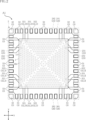
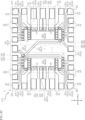
- FIG. 1 is a perspective view showing the electronic device according to the first embodiment, and shows a state seen from the bottom side.
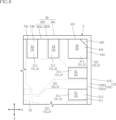
- FIG. 2 is a plan view showing the electronic device according to the first embodiment, showing a resin member with imaginary lines.
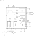
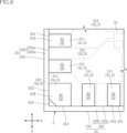
- FIG. 3 is a diagram showing electronic components and a plurality of bonding layers in imaginary lines in the plan view of FIG. 2 .
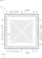
- FIG. 4 is a bottom view of the electronic device according to the first embodiment;
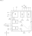
- FIG. 5 is a partial enlarged view enlarging a portion of FIG. 4 (near the first corner terminal).
- FIG. 6 is a partially enlarged view enlarging a part of FIG. 4 (near the second corner terminal).
- FIG. 7 is a partial enlarged view enlarging a part of FIG.
- FIG. 8 is a partially enlarged view enlarging a portion of FIG. 4 (near the fourth corner terminal).
- 9 is a front view of the electronic device according to the first embodiment;
- FIG. 10 is a rear view of the electronic device according to the first embodiment;
- FIG. 11 is a right side view of the electronic device according to the first embodiment;
- FIG. 12 is a left side view of the electronic device according to the first embodiment;
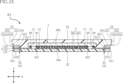
- FIG. 15 is a cross-sectional view along line XV-XV in FIG. 3.
- FIG. 16 is a cross-sectional view taken along line XVI--XVI of FIG. 3.
- FIG. 20 is a cross-sectional view showing one step of the method for manufacturing the electronic device according to the first embodiment;
- FIG. 21 is a cross-sectional view showing one step of the method for manufacturing the electronic device according to the first embodiment;
- FIG. 17 is a cross-sectional view showing one step of the method for manufacturing the electronic device according to the first embodiment;
- 18 is a cross-sectional view showing one step of the method for manufacturing the electronic device according to the first embodiment;
- FIG. 19 is a cross-sectional view showing one step of the method for manufacturing the electronic device
- FIG. 22 is a cross-sectional view showing one step of the method for manufacturing the electronic device according to the first embodiment
- FIG. 23 is a cross-sectional view showing one step of the method for manufacturing the electronic device according to the first embodiment
- FIG. FIG. 24 is a bottom view of a main part showing one step of the method of manufacturing the electronic device according to the first embodiment
- 25 is a cross-sectional view showing one step of the method for manufacturing the electronic device according to the first embodiment
- FIG. 26 is a bottom view of a main part showing one step of the method of manufacturing the electronic device according to the first embodiment
- FIG. 27 is a cross-sectional view showing one step of the method for manufacturing the electronic device according to the first embodiment
- FIG. 24 is a bottom view of a main part showing one step of the method of manufacturing the electronic device according to the first embodiment
- 25 is a cross-sectional view showing one step of the method for manufacturing the electronic device according to the first embodiment
- FIG. 26 is a bottom view of a main part showing one step of the
- FIG. 28 is a bottom view of the electronic device according to the first modification of the first embodiment;
- FIG. 29 is a cross-sectional view showing an electronic device according to a first modification of the first embodiment, corresponding to the cross-section shown in FIG. 15.
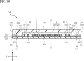
- FIG. 30 is a cross-sectional view showing an electronic device according to a first modification of the first embodiment, corresponding to the cross-section shown in FIG. 16.
- FIG. 31 is a cross-sectional view showing an electronic device according to a second modification of the first embodiment, corresponding to the cross-section shown in FIG. 13.
- FIG. 32 is a cross-sectional view showing an electronic device according to a third modification of the first embodiment, corresponding to the cross-section shown in FIG. 13.
- FIG. 33 is a cross-sectional view showing an electronic device according to a third modification of the first embodiment, corresponding to the cross-section shown in FIG. 15.
- FIG. FIG. 34 is a plan view showing the electronic device according to the fourth modification of the first embodiment, showing a resin member, an electronic component, and a plurality of bonding layers with imaginary lines.
- FIG. 35 is a partially enlarged view enlarging part of FIG. 34 (near the first corner terminal).
- 36 is a cross-sectional view taken along line XXXVI-XXXVI of FIG. 35.
- FIG. 37 is an enlarged view of a main part showing another configuration example of the electronic device according to the fourth modification of the first embodiment;
- FIG. 37 is an enlarged view of a main part showing another configuration example of the electronic device according to the fourth modification of the first embodiment; FIG.
- FIG. 38 is a bottom view of the electronic device according to the fifth modification of the first embodiment;
- FIG. FIG. 39 is a plan view showing the electronic device according to the second embodiment, showing a resin member with imaginary lines.
- FIG. 40 is a diagram showing the electronic components in imaginary lines in the plan view of FIG. 39 .
- FIG. 41 is a bottom view of the electronic device according to the second embodiment;
- FIG. 42 is a plan view showing the electronic device according to the third embodiment, and shows the resin members with imaginary lines.
- a certain entity A is formed on a certain entity B
- a certain entity A is formed on (of) an entity B
- mean a certain entity A is directly formed in a certain thing B
- a certain thing A is formed in a certain thing B while another thing is interposed between a certain thing A and a certain thing B” including.
- ⁇ an entity A is arranged on an entity B'' and ⁇ an entity A is arranged on (of) an entity B'' mean ⁇ an entity A being placed directly on a certain thing B", and "a thing A being placed on a certain thing B with another thing interposed between something A and something B" include.
- ⁇ an object A is located on (of) an object B'' means ⁇ a certain object A is in contact with an object B, and an object A is located on an object B. Being located on (of)" and "something A is located on (something) B while another thing is interposed between something A and something B including "things”.
- ⁇ a certain object A overlaps an object B when viewed in a certain direction'' means ⁇ a certain object A overlaps all of an object B'', and ⁇ a certain object A overlaps an object B.'' It includes "overlapping a part of a certain thing B".
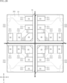
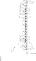
- First embodiment: 1 to 16 show an electronic device A1 according to the first embodiment.
- An electronic device A1 includes an electronic component 1, a resin member 2, and a conductive member 3. As shown in FIG.
- the thickness direction of the electronic device A1 (resin member 2) will be referred to as "thickness direction z".
- thickness direction z the thickness direction of the electronic device A1 (resin member 2)
- descriptions such as “upper”, “lower”, “upper”, “lower”, “upper surface” and “lower surface” indicate the relative positional relationship of each part, part, etc. in the thickness direction z. and is not necessarily a term that defines the relationship with the direction of gravity.
- plane view refers to the time when viewed in the thickness direction z.
- a direction orthogonal to the thickness direction z is called a "first direction x”
- a direction orthogonal to the thickness direction z and the first direction x is called a "second direction y”.
- the first direction x is the horizontal direction in the plan view of the electronic device A1 (see FIGS. 2 and 3)
- the second direction y is the plan view of the electronic device A1 (see FIGS. 2 and 3). Up-down direction.
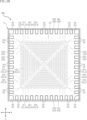
- the electronic device A1 is a surface mount type package. As shown in FIG. 1, the package structure of the electronic device A1 is, for example, a MAP type QFN. The electronic device A1 has, for example, a rectangular shape in plan view, as shown in FIGS.
- the electronic component 1 is an element that exhibits the electrical functions of the electronic device A1.
- Electronic component 1 has, for example, a rectangular shape in plan view.
- the electronic component 1 is, for example, a semiconductor element containing a semiconductor material.
- an integrated circuit element is adopted as an example of a semiconductor element.
- the electronic component 1 may be an active functional element (such as a transistor or diode) or a passive functional element (such as a resistor, capacitor or inductor) or the like, rather than an integrated circuit element.
- the electronic component 1 has an element main surface 10a and an element back surface 10b.
- the element main surface 10a and the element back surface 10b are spaced apart in the thickness direction z and face opposite sides.
- the element main surface 10a faces downward in the thickness direction z, and the element rear surface 10b faces upward in the thickness direction.
- the electronic component 1 is flip-chip mounted on the conductive member 3, and the main surface 10a of the element faces the conductive member 3 as shown in FIGS.
- the electronic component 1 has a plurality of electrodes 11 arranged on the main surface 10a of the element.
- the number, arrangement, shape and planar view size of the plurality of electrodes 11 are not limited to the illustrated example, and may be changed as appropriate according to the electronic component 1 used.
- the multiple electrodes 11 are bonded to the conductive member 3 via multiple bonding layers 19 .
- Bonding layer 19 is formed of a metal laminate, for example, in which an Sn layer is laminated on a Ni layer, and an Ag layer is further laminated on the Sn layer.
- the bonding layer 19 may be a conductive bonding material such as solder, sintered metal, or metal paste instead of this metal laminate.
- the resin member 2 is a sealing material that protects the electronic component 1.
- the resin member 2 is made of an insulating resin material.
- the resin material is, for example, black epoxy resin.
- the resin member 2 covers part of the conductive member 3 and the electronic component 1.
- the resin member 2 has a rectangular shape in plan view.
- the resin member 2 has a resin main surface 21 , a resin back surface 22 , a first resin side surface 23 , a second resin side surface 24 , a third resin side surface 25 and a fourth resin side surface 26 .
- the first resin side surface 23 and the third resin side surface 25 are separated in the first direction x as shown in FIGS. 2 to 4, 9, 10 and 15.
- FIG. The first resin side surface 23 and the third resin side surface 25 are connected to both the resin main surface 21 and the resin back surface 22 and are sandwiched between them in the thickness direction z.
- the first resin side surface 23 intersects with each of the second resin side surface 24 and the fourth resin side surface 26, as shown in FIGS.
- the first resin side surface 23 is positioned on one side in the first direction x with respect to the electronic component 1 in plan view.
- the first resin side surface 23 has a first side end surface 231 and a first resin recess 232. As shown in FIGS.
- the first side end surface 231 faces one side of the first direction x, as shown in FIGS. 9, 10 and 15 .
- the first side end surface 231 is flat.
- the first side end surface 231 forms part of the outer periphery of the resin member 2 in plan view.
- the first resin concave portion 232 is recessed from the first side end face 231 and connected to the resin back surface 22.
- the first resin recess 232 has a first wall surface 232a and a first bottom surface 232b.
- the first wall surface 232 a faces the same direction as the first side end surface 231 .
- the first wall surface 232a is located in the other direction x than the first side end surface 231, that is, in a plan view from the first side end surface 231. It is located inside the electronic device A1.
- the first bottom surface 232b connects to the first side end surface 231 and the first wall surface 232a.
- the first bottom surface 232b is flat and faces downward in the thickness direction z. Unlike this example, the first bottom surface 232b may be curved concavely.
- the third resin side surface 25 intersects with each of the second resin side surface 24 and the fourth resin side surface 26, as shown in FIGS.
- the third resin side surface 25 is connected to the edge of each of the second resin side surface 24 and the fourth resin side surface 26 opposite to the side connected to the first resin side surface 23 in the first direction x.
- the third resin side surface 25 is located on the other side of the first direction x with respect to the electronic component 1 in plan view.
- the third resin side surface 25 has a third side end surface 251 and a third resin concave portion 252 as shown in FIGS. 9, 10 and 15 .
- the third side end face 251 faces the other of the first direction x, as shown in FIGS.
- the third side end surface 251 is flat.
- the third side end surface 251 forms part of the outer periphery of the resin member 2 in plan view.
- the third resin concave portion 252 is recessed from the third side end surface 251 and connected to the resin back surface 22.
- the third resin recess 252 has a third wall surface 252a and a third bottom surface 252b.
- the third wall surface 252 a faces the same direction as the third side end surface 251 .
- the third wall surface 252a extends in the first direction x from the third side end surface 251, that is, from the third side end surface 251. It is positioned inside the electronic device A1 in plan view.
- the third bottom surface 252b connects to the third side end surface 251 and the third wall surface 252a.
- the third bottom surface 252b is flat and faces downward in the thickness direction z. Unlike this example, the third bottom surface 252b may be curved concavely.
- the second resin side surface 24 and the fourth resin side surface 26 are spaced apart in the second direction y as shown in FIGS.
- the second resin side surface 24 and the fourth resin side surface 26 are connected to both the resin main surface 21 and the resin back surface 22 and are sandwiched between them in the thickness direction z.
- the second resin side surface 24 intersects with each of the first resin side surface 23 and the third resin side surface 25, as shown in FIGS.
- the second resin side surface 24 is positioned on one side in the second direction y with respect to the electronic component 1 in plan view.
- the second resin side surface 24 has a second side end surface 241 and a second resin recess 242. As shown in FIGS.
- the second side end surface 241 faces one side of the second direction y, as shown in FIGS.
- the second side end face 241 is flat.
- the second side end surface 241 forms part of the outer periphery of the resin member 2 in plan view.
- the second resin concave portion 242 is recessed from the second side end surface 241 and connected to the resin back surface 22.
- the second resin recess 242 has a second wall surface 242a and a second bottom surface 242b.
- the second wall surface 242 a faces the same direction as the second side end surface 241 .
- the second wall surface 242a extends further in the second direction y than the second side end surface 241, that is, the second side surface 241. It is positioned inside the electronic device A1 in plan view.
- the second bottom surface 242b connects to the second side end surface 241 and the second wall surface 242a.
- the second bottom surface 242b is flat and faces downward in the thickness direction z. Unlike this example, the second bottom surface 242b may be curved concavely.
- the fourth resin side surface 26 intersects with each of the first resin side surface 23 and the third resin side surface 25, as shown in FIGS.
- the fourth resin side surface 26 is connected to the edge of each of the first resin side surface 23 and the third resin side surface 25 on the side opposite to the side connected to the second resin side surface 24 in the second direction y.
- the fourth resin side surface 26 is positioned on the other side in the second direction y with respect to the electronic component 1 in plan view.
- the fourth resin side surface 26 has a fourth side end surface 261 and a fourth resin concave portion 262 as shown in FIGS. 11, 12 and 16 .
- the fourth side end face 261 faces the other side of the second direction y, as shown in FIGS.
- the fourth side end surface 261 is flat.
- the fourth side end surface 261 forms part of the outer periphery of the resin member 2 in plan view.
- the fourth resin concave portion 262 is recessed from the fourth side end surface 261 and connected to the resin rear surface 22.
- the fourth resin recess 262 has a fourth wall surface 262a and a fourth bottom surface 262b.
- the fourth wall surface 262 a faces the same direction as the fourth side end surface 261 .
- the fourth wall surface 262a is located in the second direction y relative to the fourth side end surface 261, that is, the fourth side surface 261. It is positioned inside the electronic device A1 in plan view.
- the fourth bottom surface 262b connects to the fourth side end surface 261 and the fourth wall surface 262a.
- the fourth bottom surface 262b is flat and faces downward in the thickness direction z. Unlike this example, the fourth bottom surface 262b may be curved concavely.
- the resin member 2 includes a first resin portion 201 and a second resin portion 202.
- the first resin portion 201 and the second resin portion 202 are laminated in the thickness direction z and are in contact with each other.
- the first resin portion 201 and the second resin portion 202 are obtained by dividing the resin member 2, and are limited to those in which the boundary between the first resin portion 201 and the second resin portion 202 can be visually recognized.
- a mode in which the first resin portion 201 and the second resin portion 202 are integrated is also included.
- the first resin portion 201 is located below the second resin portion 202 in the thickness direction z.
- the lower surface of the first resin portion 201 (the surface facing downward in the thickness direction z) is the resin back surface 22 . Therefore, the first resin portion 201 has a resin rear surface 22 .
- the upper surface of the second resin portion 202 (the surface facing upward in the thickness direction z) is the main resin surface 21 . Therefore, the second resin portion 202 has a resin main surface 21 .
- the upper surface of the first resin portion 201 (the surface facing upward in the thickness direction z) and the lower surface of the second resin portion 202 (the surface facing downward in the thickness direction z) are in contact with each other.
- the conductive member 3 conducts to the electronic component 1 as appropriate.
- the conductive member 3 includes a first conductor layer 31, a second conductor layer 32 and a third conductor layer 33, as shown in FIGS. 2-8 and 13-16.
- the first conductor layer 31 penetrates the first resin portion 201 in the thickness direction z, as shown in FIGS. As shown in FIGS. 13 to 16, the first conductor layer 31 is exposed from the resin rear surface 22 and is formed on any one of the first resin side surface 23, the second resin side surface 24, the third resin side surface 25 and the fourth resin side surface 26. exposed from the heel.
- a constituent material of the first conductor layer 31 is, for example, copper or a copper alloy.
- the first conductor layer 31 includes a plurality of columnar portions 311 spaced apart from each other.
- the plurality of columnar portions 311 are prismatic, for example, and rectangular in plan view as shown in FIG. 4 . In this embodiment, each columnar portion 311 is partially exposed from the resin member 2 .
- the second conductor layer 32 is formed on the first conductor layer 31 or the first resin portion 201, as shown in FIGS.
- the second conductor layer 32 is pattern wiring.
- the constituent material of the second conductor layer 32 is, for example, copper or a copper alloy.
- the second conductor layer 32 is electrically connected to the first conductor layer 31 .
- the second conductor layer 32 includes a plurality of wiring portions 321 and a plurality of intervening portions 322, as shown in FIG.
- Each of the plurality of wiring portions 321 is a portion of the second conductor layer 32 that is electrically connected to the electronic component 1 .
- the bonding layer 19 is formed on each wiring portion 321 .
- Each of the plurality of intervening portions 322 is a portion of the second conductor layer 32 that does not conduct to the electronic component 1 .
- the multiple interposed portions 322 are sandwiched between the first conductor layer 31 and the third conductor layer 33 in the thickness direction z.
- the third conductor layer 33 is formed on the second conductor layer 32, as shown in FIGS.
- the third conductor layer 33 is partially covered with the second resin portion 202 .
- the third conductor layer 33 is exposed from any one of the first resin side surface 23 , the second resin side surface 24 , the third resin side surface 25 and the fourth resin side surface 26 .
- a constituent material of the third conductor layer 33 is, for example, copper or a copper alloy.
- the third conductor layer 33 includes a plurality of columnar portions 331 spaced apart from each other.
- the plurality of columnar portions 331 are, for example, prismatic and, as shown in FIG. 3, rectangular in plan view. In this embodiment, each columnar portion 331 is partially exposed from the resin member 2 . As understood from FIGS. 2 to 4, each of the plurality of columnar portions 331 overlaps one of the plurality of columnar portions 311 in plan view.
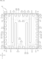
- the conductive member 3 includes a first corner terminal 41, a second corner terminal 42, a third corner terminal 43, a fourth corner terminal 44, a plurality of first lateral terminals 51, a plurality of It includes a second side terminal 52 , a plurality of third side terminals 53 and a plurality of fourth side terminals 54 .
- a first corner terminal 41 , a second corner terminal 42 , a third corner terminal 43 , a fourth corner terminal 44 , a plurality of first lateral terminals 51 , a plurality of second lateral terminals 52 , a plurality of third lateral terminals 53 and the plurality of fourth side terminals 54 are partially exposed from the resin member 2 .
- a first corner terminal 41 , a second corner terminal 42 , a third corner terminal 43 , a fourth corner terminal 44 , a plurality of first lateral terminals 51 , a plurality of second lateral terminals 52 , a plurality of third lateral terminals 53 and some of the plurality of fourth side terminals 54 are electrically connected to the electronic component 1 .
- a first corner terminal 41 , a second corner terminal 42 , a third corner terminal 43 , a fourth corner terminal 44 , a plurality of first lateral terminals 51 , a plurality of second lateral terminals 52 , a plurality of third lateral terminals 53 and the plurality of fourth side terminals 54 are respectively used when mounting the electronic device A1 on a circuit board of an electronic device or the like.
- the first corner terminal 41, the second corner terminal 42, the third corner terminal 43 and the fourth corner terminal 44 are arranged near four corners of the resin member 2 in plan view. In this embodiment, none of the first corner terminal 41 , the second corner terminal 42 , the third corner terminal 43 and the fourth corner terminal 44 are electrically connected to the electronic component 1 .
- the first square terminal 41 is exposed from the resin rear surface 22 and also exposed from the first resin side surface 23 and the second resin side surface 24.
- the first square terminal 41 includes a columnar portion 311 of the first conductor layer 31 , an intermediate portion 322 of the second conductor layer 32 and a columnar portion 331 of the third conductor layer 33 .
- the columnar portion 311 forming the first corner terminal 41 is an example of the "first columnar portion”
- the columnar portion 331 forming the first corner terminal 41 is an example of the "second columnar portion”.
- the first corner terminal 41 has a first exposed surface 411, a second exposed surface 412, a first surface 413 and a rear surface 414, as shown in FIG.
- the first exposed surface 411 is exposed from the first resin side surface 23.
- the first exposed surface 411 is exposed in the first resin recessed portion 232 of the first resin side surface 23 .
- the first exposed surface 411 faces one side in the first direction x.
- the first exposed surface 411 is flat.
- the first exposed surface 411 is flush with the first wall surface 232 a of the first resin recess 232 .
- the term “flush” means not only a mode in which two or more surfaces are ideally smooth surfaces, but also during processing in the manufacturing process of the electronic device A1 (for example, This includes the case where unevenness is inevitably formed during grinding and dicing (to be described later), and the case where processing marks are formed across the respective surfaces.
- the second exposed surface 412 is exposed from the second resin side surface 24.
- the second exposed surface 412 is exposed at the second resin recessed portion 242 of the second resin side surface 24 .
- the second exposed surface 412 faces one side in the second direction y.
- the second exposed surface 412 is flat.
- the second exposed surface 412 is flush with the second wall surface 242 a of the second resin recess 242 .
- the first surface 413 is connected to both the first exposed surface 411 and the second exposed surface 412 in plan view.
- the first surface 413 is covered with the resin member 2 .
- first surface 413 is flat and slopes with respect to each of first exposed surface 411 and second exposed surface 412 .
- the first surface 413 may be curved to be concave or convex in plan view.
- the back surface 414 faces downward in the thickness direction z.
- the back surface 414 is exposed from the resin back surface 22 as shown in FIG.
- Back surface 414 is flat.
- the back surface 414 is flush with the resin back surface 22 .
- the first square terminal 41 further has a covering surface 419 .
- the covering surface 419 is formed on the side opposite to the first surface 413 .
- Cover surface 419 is covered with resin member 2 .
- Cover surface 419 is flat.
- Covering surface 419 is formed, for example, on columnar portion 311 of first corner terminal 41 , and is not formed on intervening portion 322 and columnar portion 331 of first corner terminal 41 .
- the covering surface 419 may be formed across the columnar portion 311 of the first square terminal 41 and the intermediate portion 322 , or further across the columnar portion 331 .
- the covering surface 419 is provided on the first corner terminal 41 as a mark indicating the orientation of the electronic device A1.
- the covering surface 419 is not the first corner terminal 41 , but the second corner terminal 42 , the third corner terminal 43 , the fourth corner terminal 44 , the plurality of first side terminals 51 , and the plurality of second side terminals 52 . , the plurality of third side terminals 53 and the plurality of fourth side terminals 54 .
- the second corner terminals 42 are exposed from the resin rear surface 22 and also exposed from the second resin side surface 24 and the third resin side surface 25 respectively.
- the second corner terminal 42 includes a columnar portion 311 of the first conductor layer 31 , an intermediate portion 322 of the second conductor layer 32 and a columnar portion 331 of the third conductor layer 33 .
- the second corner terminal 42 has a third exposed surface 421, a fourth exposed surface 422, a second surface 423 and a rear surface 424, as shown in FIG.
- the third exposed surface 421 is exposed from the second resin side surface 24.
- the third exposed surface 421 is exposed at the second resin recessed portion 242 of the second resin side surface 24 .
- the third exposed surface 421 faces one side in the second direction y.
- the third exposed surface 421 is flat.
- the third exposed surface 421 is flush with the second wall surface 242 a of the second resin recess 242 .
- the fourth exposed surface 422 is exposed from the third resin side surface 25.
- the fourth exposed surface 422 is exposed in the third resin recessed portion 252 of the third resin side surface 25 .
- the fourth exposed surface 422 faces the other side of the first direction x.
- the fourth exposed surface 422 is flat.
- the fourth exposed surface 422 is flush with the third wall surface 252 a of the third resin recess 252 .
- the second surface 423 is connected to both the third exposed surface 421 and the fourth exposed surface 422 in plan view.
- the second surface 423 is covered with the resin member 2 .
- the second surface 423 is flat and slopes with respect to each of the third exposed surface 421 and the fourth exposed surface 422 .
- the second surface 423 may be curved such that it is concave in plan view or convex in plan view.
- the back surface 424 faces downward in the thickness direction z.
- the back surface 424 is exposed from the resin back surface 22 as shown in FIG.
- Back surface 424 is flat.
- the back surface 424 is flush with the resin back surface 22 .
- the third corner terminal 43 is exposed from the resin rear surface 22 and is also exposed from the third resin side surface 25 and the fourth resin side surface 26 respectively.
- the third corner terminal 43 includes a columnar portion 311 of the first conductor layer 31 , an intermediate portion 322 of the second conductor layer 32 and a columnar portion 331 of the third conductor layer 33 .
- the third corner terminal 43 has a fifth exposed surface 431 , a sixth exposed surface 432 , a third surface 433 and a rear surface 434 .
- the fifth exposed surface 431 is exposed from the third resin side surface 25.
- the fifth exposed surface 431 is exposed in the third resin recessed portion 252 of the third resin side surface 25 .
- the fifth exposed surface 431 faces the other side of the first direction x.
- the fifth exposed surface 431 is flat.
- the fifth exposed surface 431 is flush with the third wall surface 252 a of the third resin recess 252 .
- the sixth exposed surface 432 is exposed from the fourth resin side surface 26.
- the sixth exposed surface 432 is exposed at the fourth resin recessed portion 262 of the fourth resin side surface 26 .
- the sixth exposed surface 432 faces the other side of the second direction y.
- the sixth exposed surface 432 is flat.
- the sixth exposed surface 432 is flush with the fourth wall surface 262 a of the fourth resin recess 262 .
- the third surface 433 is connected to both the fifth exposed surface 431 and the sixth exposed surface 432 in plan view.
- the third surface 433 is covered with the resin member 2 .
- the third surface 433 is flat and slopes with respect to each of the fifth exposed surface 431 and the sixth exposed surface 432 .
- the third surface 433 may be curved so as to be concave or convex in plan view.
- the back surface 434 faces downward in the thickness direction z.
- the back surface 434 is exposed from the resin back surface 22 as shown in FIG.
- Back surface 434 is flat.
- the back surface 434 is flush with the resin back surface 22 .
- the fourth corner terminal 44 is exposed from the resin back surface 22 and also exposed from the fourth resin side surface 26 and the first resin side surface 23 .
- the fourth corner terminal 44 includes a columnar portion 311 of the first conductor layer 31 , an intermediate portion 322 of the second conductor layer 32 and a columnar portion 331 of the third conductor layer 33 .
- the fourth corner terminal 44 has a seventh exposed surface 441 , an eighth exposed surface 442 , a fourth surface 443 and a rear surface 444 .
- the seventh exposed surface 441 is exposed from the fourth resin side surface 26.
- the seventh exposed surface 441 is exposed in the fourth resin recessed portion 262 of the fourth resin side surface 26 .
- the seventh exposed surface 441 faces the other side of the second direction y.
- the seventh exposed surface 441 is flat.
- the seventh exposed surface 441 is flush with the fourth wall surface 262 a of the fourth resin recess 262 .
- the eighth exposed surface 442 is exposed from the first resin side surface 23.
- the eighth exposed surface 442 is exposed in the first resin recessed portion 232 of the first resin side surface 23 .
- the eighth exposed surface 442 faces one side in the first direction x.
- the eighth exposed surface 442 is flat.
- the eighth exposed surface 442 is flush with the first wall surface 232 a of the first resin recess 232 .
- the fourth surface 443 is connected to both the seventh exposed surface 441 and the eighth exposed surface 442 in plan view.
- the fourth surface 443 is covered with the resin member 2 .
- the fourth surface 443 is flat and slopes with respect to each of the seventh exposed surface 441 and the eighth exposed surface 442 .
- the fourth surface 443 may be curved so as to be concave or convex in plan view.
- the back surface 444 faces downward in the thickness direction z.
- the back surface 444 is exposed from the resin back surface 22 as shown in FIG.
- Back surface 444 is flat.
- the back surface 444 is flush with the resin back surface 22 .
- the fifth exposed surface 431, the sixth exposed surface 432 and the rear surface 434, and the seventh exposed surface 441, the eighth exposed surface 442 and the rear surface 444 of the fourth corner terminal 44 are each covered with a plating layer (not shown).
- the plating layer is formed to improve the wettability of solder.
- the solder is used, for example, when mounting the electronic device A1 on a circuit board of an electronic device or the like.
- the plated layer includes, for example, a Ni layer, a Pd layer and an Au layer formed by electroless plating, which will be described later.
- the constituent material of the plated layer is not limited to this.
- the plurality of first side terminals 51 are arranged along the first resin side surface 23, as shown in FIGS. Therefore, the plurality of first side terminals 51 are arranged in the second direction y.
- the plurality of first side terminals 51 are sandwiched between the first corner terminal 41 and the second corner terminal 42 in the second direction y and positioned between the first corner terminal 41 and the second corner terminal 42 .
- the plurality of first side terminals 51 are exposed from the first resin side surface 23 while being exposed from the resin back surface 22 . Some of the plurality of first side terminals 51 are electrically connected to the electronic component 1 and some are not electrically connected to the electronic component 1 .
- those that are electrically connected to the electronic component 1 include each columnar portion 311 , each wiring portion 321 and each columnar portion 331 .
- those that are not electrically connected to the electronic component 1 are configured to include each columnar portion 311 , each intermediate portion 322 and each columnar portion 331 .
- Each of the plurality of first side terminals 51 includes an exposed surface 511 and a back surface 512, as shown in FIGS. Each of the plurality of first side terminals 51 is covered with the resin member 2 on the surfaces other than the exposed surface 511 and the back surface 512 .
- each first side terminal 51 is exposed from the first resin side surface 23 .
- the exposed surface 511 is exposed in the first resin recessed portion 232 of the first resin side surface 23 .
- the exposed surface 511 is flat.
- the exposed surface 511 is flush with the first wall surface 232 a of the first resin recess 232 .
- each first side terminal 51 the rear surface 512 is exposed from the resin rear surface 22, as shown in FIGS.
- the back surface 512 is flush with the resin back surface 22 .
- the back surface 512 connects to the exposed surface 511 .
- the plurality of second side terminals 52 are arranged along the second resin side surface 24, as shown in FIGS. Therefore, the plurality of second side terminals 52 are arranged in the first direction x.
- the plurality of second side terminals 52 are sandwiched between the first corner terminal 41 and the second corner terminal 42 in the first direction x and positioned between the first corner terminal 41 and the second corner terminal 42 .
- the plurality of second side terminals 52 are exposed from the second resin side surface 24 while being exposed from the resin back surface 22 . Some of the plurality of second side terminals 52 are electrically connected to the electronic component 1 and some are not electrically connected to the electronic component 1 .
- those that are electrically connected to the electronic component 1 include each columnar portion 311 , each wiring portion 321 and each columnar portion 331 .
- those that are not electrically connected to the electronic component 1 are configured to include each columnar portion 311 , each intermediate portion 322 and each columnar portion 331 .
- Each of the plurality of second side terminals 52 includes an exposed surface 521 and a rear surface 522, as shown in FIGS. Each of the plurality of second side terminals 52 is covered with the resin member 2 on the surfaces other than the exposed surface 521 and the back surface 522 .
- each second side terminal 52 is exposed from the second resin side surface 24 .
- the exposed surface 521 is exposed in the second resin recessed portion 242 of the second resin side surface 24 .
- the exposed surface 521 is flat.
- the exposed surface 521 is flush with the second wall surface 242 a of the second resin recess 242 .
- each second side terminal 52 the rear surface 522 is exposed from the resin rear surface 22, as shown in FIGS.
- the back surface 522 is flush with the resin back surface 22 .
- the back surface 522 connects to the exposed surface 521 .
- the plurality of third side terminals 53 are arranged along the third resin side surface 25, as shown in FIGS. Therefore, the plurality of third side terminals 53 are arranged in the second direction y.
- the plurality of third side terminals 53 are sandwiched between the second corner terminal 42 and the third corner terminal 43 and positioned between the second corner terminal 42 and the third corner terminal 43 in the second direction y.
- the plurality of third side terminals 53 are exposed from the third resin side surface 25 while being exposed from the resin back surface 22 .
- Some of the plurality of third side terminals 53 are electrically connected to the electronic component 1 and some are not electrically connected to the electronic component 1 .
- those that are electrically connected to the electronic component 1 include each columnar portion 311 , each wiring portion 321 and each columnar portion 331 .
- those that are not electrically connected to the electronic component 1 include each columnar portion 311 , each intermediate portion 322 and each columnar portion 331 .
- Each of the plurality of third side terminals 53 includes an exposed surface 531 and a rear surface 532, as shown in FIGS.
- the surfaces other than the exposed surface 531 and the back surface 532 of each of the plurality of third side terminals 53 are covered with the resin member 2 .
- each third side terminal 53 is exposed from the third resin side surface 25 .
- the exposed surface 531 is exposed in the third resin recessed portion 252 of the third resin side surface 25 .
- the exposed surface 531 is flat.
- the exposed surface 531 is flush with the third wall surface 252 a of the third resin recess 252 .
- each third side terminal 53 the back surface 532 is exposed from the resin back surface 22, as shown in FIGS.
- the back surface 532 is flush with the resin back surface 22 .
- the back surface 532 connects to the exposed surface 531 .
- the plurality of fourth side terminals 54 are arranged along the fourth resin side surface 26, as shown in FIGS. Therefore, the plurality of fourth side terminals 54 are arranged in the first direction x.
- the plurality of fourth side terminals 54 are sandwiched between the third corner terminal 43 and the fourth corner terminal 44 in the first direction x and positioned between the third corner terminal 43 and the fourth corner terminal 44 .
- the plurality of fourth side terminals 54 are exposed from the fourth resin side surface 26 while being exposed from the resin back surface 22 . Some of the plurality of fourth side terminals 54 are electrically connected to the electronic component 1 and some are not electrically connected to the electronic component 1 .
- those that are electrically connected to the electronic component 1 include each columnar portion 311 , each wiring portion 321 and each columnar portion 331 .
- those that are not electrically connected to the electronic component 1 are configured to include each columnar portion 311 , each intermediate portion 322 and each columnar portion 331 .
- Each of the plurality of fourth side terminals 54 includes an exposed surface 541 and a rear surface 542, as shown in FIGS. Each of the plurality of fourth side terminals 54 is covered with the resin member 2 on the surfaces other than the exposed surface 541 and the back surface 542 .
- each fourth side terminal 54 is exposed from the fourth resin side surface 26 .
- the exposed surface 541 is exposed in the fourth resin recessed portion 262 of the fourth resin side surface 26 .
- the exposed surface 541 is flat.
- the exposed surface 541 is flush with the fourth wall surface 262 a of the fourth resin recess 262 .
- each fourth side terminal 54 the rear surface 542 is exposed from the resin rear surface 22, as shown in FIGS.
- the back surface 542 is flush with the resin back surface 22 .
- the back surface 542 connects to the exposed surface 541 .
- the exposed surface 541 and the rear surface 542 of the 4-side terminal 54 are each covered with a plating layer (not shown).
- the plating layer is formed to improve the wettability of solder.
- the solder is used, for example, when mounting the electronic device A1 on a circuit board of an electronic device or the like.
- the plated layer includes, for example, a Ni layer, a Pd layer and an Au layer formed by electroless plating, which will be described later.
- the constituent material of the plated layer is not limited to this.
- FIG. 17 to 23, 25 and 27 are cross-sectional views showing one step of the method of manufacturing the electronic device A1, and correspond to the cross-section of the electronic device A1 shown in FIG. 24 and 26 are enlarged plan views of essential parts showing one step of the method of manufacturing the electronic device A1.
- each electronic device A1 in the process of being manufactured is arranged with its bottom facing upward in the thickness direction z. .
- a support substrate 90 is prepared, and the first conductor layer 31 is formed on the prepared support substrate 90 .
- a silicon substrate for example, is adopted as the support substrate 90 .
- the support substrate 90 may be a glass substrate instead of a silicon substrate.
- the support substrate 90 to be prepared has a size that allows a plurality of electronic devices A1 to be arranged vertically and horizontally in a matrix in plan view.
- a metal film made of copper or a copper alloy is formed by sputtering. Thereafter, a resist layer is patterned on the metal film by photolithography, and a plurality of metal columns made of copper or copper alloy are formed on the metal film exposed from the resist layer by electroplating. After removing the resist layer, the metal film exposed from the plurality of metal pillars is removed. Thereby, the first conductor layer 31 including the plurality of columnar portions 311 is formed.
- a first resin portion 201 is formed so as to cover the first conductor layer 31 formed on the support substrate 90.
- First resin portion 201 is an electrically insulating resin, and is made of, for example, epoxy resin or polyimide.
- the first resin portion 201 is formed by molding, for example.
- the first resin portion 201 is ground from the upper surface to expose the top surface of the first conductor layer 31 .
- the ground upper surface of the first resin portion 201 serves as a boundary with the second resin portion 202 to be formed later.
- a whetstone, for example, is used for grinding.
- the second conductor layer 32 , the plurality of bonding layers 19 and the third conductor layer 33 are formed on the top surface of the first resin portion 201 .
- the following five treatments first treatment to fifth treatment are performed.
- a seed layer is uniformly formed on the top surface of the first resin portion 201 .
- the seed layer is, for example, a metal thin film formed by sputtering.
- the metal thin film is made of, for example, nickel or chromium.
- a patterned resist layer is formed by photolithography on the seed layer formed in the first process, and copper or copper alloy is deposited by electroplating on the seed layer exposed from the resist layer. Thereby, the second conductor layer 32 connected by the seed layer is formed.
- a patterned resist layer is formed by photolithography on the second conductor layer 32 formed in the second process, and a Ni layer is formed by electroplating on the second conductor layer 32 exposed from the resist layer. , Sn layer and Ag layer are laminated in order. Then, the resist layer is removed. Thereby, a plurality of bonding layers 19 are formed.
- a patterned resist layer is formed by photolithography on the second conductor layer 32 formed in the second process, and the second conductor layer 32 exposed from the resist layer is electroplated with copper or copper. A plurality of metal columns made of a copper alloy are formed. Then, the resist layer is removed. Thereby, the third conductor layer 33 including the plurality of columnar portions 331 is formed.
- portions of the seed layer formed in the first process that are exposed from the second conductor layer 32, the plurality of bonding layers 19, and the third conductor layer 33 are removed.
- the second conductor layer 32 divided into a plurality of wiring portions 321 and a plurality of intervening portions 322 is formed from the second conductor layer 32 connected by the seed layer.
- the electronic component 1 is mounted on the second conductor layer 32 with the bonding layer 19 interposed therebetween.
- each electrode 11 arranged on the element main surface 10a is joined to the second conductor layer 32 via each bonding layer 19, and the element main surface 10a is in a posture facing the second conductor layer 32.
- An electronic component 1 is mounted. That is, the electronic component 1 is flip-chip mounted on the support substrate 90 via the first resin portion 201, the second conductor layer 32, the bonding layers 19, and the like.
- a second resin portion 202 is formed so as to cover the first resin portion 201, the second conductor layer 32, the third conductor layer 33, the plurality of bonding layers 19, and the electronic component 1.
- the second resin portion 202 is an electrically insulating resin, and is made of, for example, epoxy resin or polyimide.
- the second resin portion 202 is formed by molding, for example.
- the support substrate 90 is ground downward toward the second resin portion 202, and the support substrate 90 is removed. At this time, the grinding is performed until the first resin portion 201 has a predetermined thickness. This grinding exposes the bottom surface of each columnar portion 311 from the first resin portion 201 .
- FIGS. 24 and 25 half-cut dicing is performed to form grooves 91 having a lattice shape in plan view.
- 24 shows the state before half-cut dicing
- FIG. 25 shows the state after half-cut dicing.
- dots indicate areas to be half-cut diced.
- the dicing blade is moved in the direction indicated by the arrow shown in FIG. 24 (first dicing direction).
- first dicing direction In the first dicing direction along the first direction x, as shown in FIG. 24, the direction from the other side of the first direction x to the one side of the first direction x is the advancing direction of the dicing blade.
- the first dicing direction along the second direction y as shown in FIG.
- the direction from the other side of the second direction y to one side of the second direction y is the traveling direction of the dicing blade.
- half-cut diced regions are indicated by imaginary lines.
- first, the dicing blade is moved along the first dicing direction along the first direction x. This dicing is called "preceding first dicing".
- strip-shaped portions along the first direction x are formed in the grooves 91, and the strip-shaped portions along the first direction x have the second exposed surface 412, the third exposed surface 421, A sixth exposed surface 432 and a seventh exposed surface 441 are formed.
- the dicing blade is moved along the first dicing direction along the second direction y.
- This dicing is referred to as "second attack first dicing".
- second dicing a streak-like portion along the second direction y is formed in the groove 91, and the first exposed surface 411 and the fourth exposed surface 422 are formed in the streak-like portion along the second direction y. , a fifth exposed surface 431 and an eighth exposed surface 442 are formed.
- grooves 91 formed in half-cut dicing are formed by resin member 2 (first resin portion 201 and second resin portion 202), first conductor layer 31, second conductor layer 32 and third conductor layer 32. It straddles the conductor layer 33 .
- the surfaces of the first conductor layer 31, the second conductor layer 32, and the third conductor layer 33 exposed from the resin back surface 22 and the grooves 91 are plated.
- a Ni layer, a Pd layer and an Au layer are deposited in order by electroless plating.
- a plated layer composed of a Ni layer, a Pd layer and an Au layer is formed on the seventh exposed surface 441 , the eighth exposed surface 442 and the rear surface 444 .
- FIGS. 26 and 27 show the electronic components 1 individually separated by full-cut dicing (cutting).
- 26 shows the state before full-cut dicing
- FIG. 27 shows the state after full-cut dicing.
- dots indicate areas to be full-cut diced.
- the dicing blade is moved in the direction indicated by the arrow shown in FIG. 26 (second dicing direction).
- the second dicing direction along the first direction x as shown in FIG. 26
- the direction from the other side of the first direction x to the one side of the first direction x is the advancing direction of the dicing blade.
- the second dicing direction along the second direction y as shown in FIG.
- the direction from the other side of the second direction y to the one side of the second direction y is the traveling direction of the dicing blade.
- a dicing blade used in full-cut dicing is thinner than a dicing blade used in half-cut dicing.
- the phantom line indicates the full-cut diced region.
- the dicing blade is moved along the second dicing direction along the first direction x. This dicing is called "preceding second dicing".
- a second side end face 241 and a fourth side end face 261 are formed by the preceding second dicing.
- the dicing blade is moved along the second dicing direction along the second direction y. This dicing is called "second attack second dicing".
- the first side end surface 231 and the third side end surface 251 are formed by the second dicing performed later.
- the first corner terminal 41 has a first exposed surface 411, a second exposed surface 412 and a first surface 413.
- the first exposed surface 411 is exposed from the first resin side surface 23 and the second exposed surface 412 is exposed from the second resin side surface 24 .
- the first surface 413 is connected to the first exposed surface 411 and the second exposed surface 412 and covered with the resin member 2 .
- the first exposed surface 411 is formed during the preceding first dicing in half-cut dicing
- the second exposed surface 412 is formed during the subsequent first dicing in half-cut dicing.
- first dicing and subsequent dicing are performed.
- Each terminal end of the second dicing overlaps a corner portion where the first exposed surface 411 and the second exposed surface 412 are connected.
- the corner portion where the first exposed surface 411 and the second exposed surface 412 are connected is subjected to a total of two processing loads during dicing. Therefore, the impact and stress applied to the first square terminal 41 are increased, and the possibility that the first square terminal 41 is peeled off is increased.
- the first square terminal 41 has the first surface 413, and the first surface 413 is covered with the resin member 2.
- Each end portion of the time becomes the resin member 2 instead of the first square terminal 41 .
- impact and stress applied to the first square terminal 41 are suppressed. Therefore, in the electronic device A ⁇ b>1 , it is possible to prevent the first square terminal 41 from peeling off from the resin member 2 .
- the second corner terminal 42 has a second surface 423 connected to a third exposed surface 421 and a fourth exposed surface 422, and the third corner terminal 43 has a fifth exposed surface 431 and a sixth exposed surface. 432 , and the fourth corner terminal 44 has a fourth surface 443 connected to the seventh exposed surface 441 and the eighth exposed surface 442 .
- the second surface 423 , the third surface 433 and the fourth surface 443 are each covered with the resin member 2 . According to this configuration, in the electronic device A1, in addition to the first corner terminal 41, the second corner terminal 42, the third corner terminal 43, and the fourth corner terminal 44 can also be prevented from peeling off from the resin member 2.
- the terminals (the first corner terminal 41, the second corner terminal 42, the third corner terminal 43, and the fourth corner terminal 44) arranged near the four corners of the resin member 2 in plan view are respectively Separation from the resin member 2 can be suppressed.
- the first exposed surface 411, the second exposed surface 412, the third exposed surface 421, the fourth exposed surface 422, the fifth exposed surface 431, the sixth exposed surface 432, the seventh exposed surface 441, the eighth exposed surface A plating layer is formed on the surface 442, each exposed surface 511, each exposed surface 521, each exposed surface 531, and each exposed surface 541, respectively.
- a solder fillet is formed on the surface 442, each exposed surface 511, each exposed surface 521, each exposed surface 531, and each exposed surface 541, respectively.
- the first square terminal 41 includes a columnar portion 331. According to this configuration, the first square terminal 41 has a larger dimension along the thickness direction z than when the columnar portion 331 is not included. Thereby, the areas of the first exposed surface 411 and the second exposed surface 412 can be increased. The first exposed surface 411 and the second exposed surface 412 come into contact with a bonding material such as solder when the electronic device A1 is mounted on a circuit board such as an electronic device. In other words, since the contact area of the bonding material is increased, the electronic device A1 can increase the bonding strength to the circuit board of the electronic device or the like.
- the first square terminal 41 does not conduct to the electronic component 1.
- the first square terminal 41 that does not conduct to the electronic component 1 may not be provided in the electronic device A1 from an electrical point of view.
- the electronic device A1 includes the first corner terminals 41, it is possible to widen the bonding area by soldering or the like when mounting the electronic device A1 on a circuit board of an electronic device or the like.
- the first square terminal 41 allows the electronic device A1 to increase the mounting strength on a circuit board of an electronic device or the like. This is the same for the second corner terminal 42, the third corner terminal 43 and the fourth corner terminal 44 as well.
- the electronic device A2 differs from the electronic device A1 in the following points.
- the first resin side surface 23 of the electronic device A2 does not include the first resin recess 232 .
- the second resin side surface 24 of the electronic device A2 does not include the second resin recess 242 .
- the third resin side surface 25 of the electronic device A2 does not include the third resin recess 252 .
- the fourth resin side surface 26 of the electronic device A2 does not include the fourth resin recess 262 .
- the electronic device A2 shown in FIGS. 28 to 30 can be manufactured, for example, in the manufacturing method of the electronic device A1 without half-cut dicing.
- the back surface 414 of the first square terminal 41, the back surface 424 of the second square terminal 42, the back surface 434 of the third square terminal 43, and the back surface 434 of the third square terminal 43 are formed by the electroless plating.
- plating eg Ni, Pd and Au layers
- the first exposed surface 411 and the second exposed surface 412 are formed on the first corner terminal 41 by full-cut dicing. Further, by full-cut dicing, the second corner terminal 42 is formed with a third exposed surface 421 and a fourth exposed surface 422, the third corner terminal 43 is formed with a fifth exposed surface 431 and a sixth exposed surface 432, and the fourth corner terminal 44 is formed. A seventh exposed surface 441 and an eighth exposed surface 442 are respectively formed on the .
- the first corner terminal 41 has a first surface 413, the first surface 413 is connected to the first exposed surface 411 and the second exposed surface 412, and the resin member covered by 2. Therefore, in the electronic device A2, like the electronic device A1, the terminals exposed from the resin member 2 (the first corner terminals 41, etc.) can be prevented from peeling off. This is the same for the second corner terminal 42, the third corner terminal 43 and the fourth corner terminal 44 as well. It should be noted that the electronic device A2 achieves the same effects as the electronic device A1 due to the configuration common to the electronic device A1.
- FIG. 31 shows an electronic device A3 according to the second modification of the first embodiment.
- the electronic device A3 differs from the electronic device A1 in that the second conductor layer 32 does not include each intervening portion 322 .
- each of the first corner terminal 41 and the third corner terminal 43 has a columnar portion 331 formed on the columnar portion 311 and in contact with the columnar portion 311 .
- each of the second corner terminal 42 and the fourth corner terminal 44 also has a columnar portion 331 formed on the columnar portion 311 and in contact with the columnar portion 311 .
- those that are not electrically connected to the electronic component 1 are columnar.
- a portion 331 is formed on the columnar portion 311 and contacts the columnar portion 311 .
- the first corner terminal 41 has a first surface 413, the first surface 413 is connected to the first exposed surface 411 and the second exposed surface 412, and the resin member covered by 2. Therefore, in the electronic device A3, like the electronic device A1, the terminals exposed from the resin member 2 (the first corner terminal 41, etc.) can be prevented from peeling off. This is the same for the second corner terminal 42, the third corner terminal 43 and the fourth corner terminal 44 as well. It should be noted that the electronic device A3 achieves the same effects as the electronic devices A1 and A2 due to the configuration common to the electronic devices A1 and A2.
- FIG 32 and 33 show an electronic device A4 according to the third modified example of the first embodiment.
- the electronic device A4 differs from the electronic device A1 in that the third conductor layer 33 (each columnar portion 331) is not provided.
- the conductive member 3 does not include the third conductor layer 33, so as shown in FIG. is not formed.
- the second corner terminal 42 and the fourth corner terminal 44 also do not have the columnar portion 331 formed on the intervening portion 322 .
- each of the plurality of first side terminals 51, the plurality of second side terminals 52, the plurality of third side terminals 53, and the plurality of fourth side terminals 54 , the columnar portion 331 is not formed on the wiring portion 321 or the intervening portion 322 .
- the first corner terminal 41 has a first surface 413, the first surface 413 is connected to the first exposed surface 411 and the second exposed surface 412, and the resin member covered by 2. Therefore, in the electronic device A4, like the electronic device A1, the terminals exposed from the resin member 2 (the first corner terminals 41, etc.) can be prevented from peeling off. This is the same for the second corner terminal 42, the third corner terminal 43 and the fourth corner terminal 44 as well. However, for example, in the electronic device A ⁇ b>1 , the areas of the first exposed surface 411 and the second exposed surface 412 of the first square terminal 41 are increased by the columnar portions 331 .
- the electronic device A1 mounting strength on a circuit board of an electronic device or the like is enhanced.
- the improvement of the mounting strength by such a columnar portion 331 is achieved by the second corner terminal 42, the third corner terminal 43, the fourth corner terminal 44, the plurality of first side terminals 51, the plurality of second side terminals 52, the plurality of The same applies to each of the third side terminal 53 and the plurality of fourth side terminals 54 of .
- the electronic device A1 is preferable to the electronic device A4 in terms of improving the mounting strength. It should be noted that the electronic device A4 has the same effect as each of the electronic devices A1 to A3 due to the structure common to each of the electronic devices A1 to A3.
- 34 to 36 show an electronic device A5 according to the fourth modification of the first embodiment.
- the shapes of the columnar portions 331 of the first corner terminal 41, the second corner terminal 42, the third corner terminal 43, and the fourth corner terminal 44 are different from those of the electronic device A1.
- the columnar portion 331 of the first corner terminal 41 is divided into two parts. Therefore, the first corner terminal 41 further includes an exposed area 415 .
- the exposed area 415 is exposed from the columnar portion 331 of the first corner terminal 41 in plan view. In this embodiment, the exposed region 415 is part of the upper surface of the intervening portion 322 (the surface facing upward in the thickness direction z).
- the exposed region 415 is a part of the upper surface of the columnar portion 311 (the surface facing upward in the thickness direction z). is.
- the exposed region 415 overlaps the first surface 413 in plan view.
- the exposed region 415 extends in a direction orthogonal to the first surface 413 in plan view.
- the second corner terminal 42 further includes an exposed area 425, as shown in FIG.
- Third corner terminal 43 further includes an exposed area 435 .
- Fourth corner terminal 44 further includes an exposed area 445 .
- a dot is drawn in each exposed area 425, 435, 445.
- the exposed region 425 is exposed from the columnar portion 331 of the second corner terminal 42 in plan view.
- the exposed region 435 is exposed from the columnar portion 331 of the third corner terminal 43 in plan view.
- the exposed region 445 is exposed from the columnar portion 331 of the fourth corner terminal 44 in plan view.
- Each of the exposed regions 425, 435, 445 is configured similarly to the exposed region 415 in plan view.
- the first corner terminal 41 has a first surface 413, the first surface 413 is connected to the first exposed surface 411 and the second exposed surface 412, and the resin member covered by 2. Therefore, in the electronic device A5, like the electronic device A1, the terminals exposed from the resin member 2 (the first corner terminals 41, etc.) can be prevented from peeling off. This is the same for the second corner terminal 42, the third corner terminal 43 and the fourth corner terminal 44 as well. It should be noted that the electronic device A5 has the same effect as each of the electronic devices A1 to A4 due to the structure common to each of the electronic devices A1 to A4.
- the first corner terminal 41 has the columnar portion 331 divided into two parts and further includes an exposed area 415.
- resin member 2 is formed so as to be in contact with exposed region 415 .
- the electronic device A5 can increase the bonding strength between the resin member 2 and the first corner terminal 41 by the anchor effect.
- the electronic device A5 can further suppress peeling of the first corner terminal 41 compared to the electronic device A1. This is the same for the second corner terminal 42, the third corner terminal 43 and the fourth corner terminal 44 as well.
- FIG. 37 shows an example in which the columnar portion 331 of the first corner terminal 41 has a different shape from the example shown in the electronic device A5.
- the exposed region 415 includes a region along the first surface 413 in plan view.
- the electronic device shown in FIG. 37 also has the same effects as the electronic device A5.
- FIG. 38 shows an electronic device A6 according to the fifth modification of the first embodiment.
- the electronic device A6 differs from the electronic device A1 in the following points.
- First, the second corner terminal 42 of the electronic device A6 does not have the second surface 423 .
- Second, the third corner terminal 43 of the electronic device A6 does not have the third surface 433 .
- Thirdly, the fourth corner terminal 44 of the electronic device A6 does not have the fourth surface 443 .
- the first corner terminal 41 is cut after the second corner terminal 42, the third corner terminal 43, and the fourth corner terminal 44, for example, during half-cut dicing.
- the vibration and stress applied to the first corner terminal 41 during dicing are applied to the other second corner terminal 42, the third corner terminal 43, and the fourth corner terminal 44, respectively. and stress.
- the first surface 413 is provided only on the first corner terminals 41 that are highly likely to be peeled off.
- the first corner terminal 41 has a first surface 413, the first surface 413 is connected to the first exposed surface 411 and the second exposed surface 412, and the resin member covered by 2. Therefore, in the electronic device A6, like the electronic device A1, the terminals exposed from the resin member 2 (the first corner terminal 41, etc.) can be prevented from peeling off. It should be noted that the electronic device A6 has the same effect as each of the electronic devices A1 to A5 due to the structure common to each of the electronic devices A1 to A5.
- the first corner terminal 41 which is most likely to be separated from the resin member 2 is provided with the first surface 413.
- the second corner terminal 42 is provided with the second surface 423.
- the third corner terminal 43 may be provided with the third surface 433
- the fourth corner terminal 44 may be provided with the fourth surface 443 .
- two (or three) that are relatively likely to be peeled off from the resin member 2 are selected. select.
- the first corner terminal 41 and the fourth corner terminal 44 to be cut during the second dicing are two relatively high ones.
- any of the first surface 413, the second surface 423, the third surface 433, or the fourth surface 443 may then be formed on the selected one as appropriate. In other words, it is not necessary to form the first surface 413, the second surface 423, the third surface 433, or the fourth surface 443 on the part that is relatively unlikely to be peeled off from the resin member 2.
- Second embodiment 39 to 41 show an electronic device B1 according to the second embodiment.
- the electronic device B1 differs from the electronic device A1 in the following points.
- the electronic device B1 mainly differs in the configuration of the conductive member 3 .
- the first square terminal 41 is electrically connected to the electronic component 1, as shown in FIGS. Therefore, the first corner terminal 41 includes the wiring portion 321 instead of the intervening portion 322 compared to the first corner terminal 41 of the electronic device A1. Further, in the electronic device B1, as shown in FIGS. 39 to 41, the plurality of first side terminals 51, the plurality of second side terminals 52, the plurality of third side terminals 53 and the plurality of fourth side terminals All terminals 54 are electrically connected to the electronic component 1 .
- the first corner terminal 41 has the first face 413 as in the electronic device A1. According to this configuration, the electronic device B1 can suppress peeling of the first corner terminal 41 from the resin member 2 in the same manner as the electronic device A1. Further, in the electronic device B1, similarly to the electronic device A1, the second corner terminal 42 has the second surface 423, the third corner terminal 43 has the third surface 433, and the fourth corner terminal 44 has the fourth surface. It has a face 443 . Therefore, the electronic device B1 can suppress peeling of the second corner terminal 42, the third corner terminal 43, and the fourth corner terminal 44 from the resin member 2, similarly to the electronic device A1. Note that the electronic device B1 has the same effects as the electronic devices A1 to A6 due to the configuration common to the electronic devices A1 to A6.
- Third embodiment: 42 to 44 show an electronic device C1 according to the third embodiment.
- the electronic device C1 differs from the electronic devices A1 and B1 in the following points.
- First, the electronic device C1 comprises two electronic components 1 .
- two electronic components 1 are spaced apart in the first direction x, for example.
- a first corner terminal 41, a second corner terminal 42, a third corner terminal 43, a fourth corner terminal 44, a plurality of first lateral terminals 51, a plurality of Each of the second side terminal 52 , the plurality of third side terminals 53 and the plurality of fourth side terminals 54 is electrically connected to one of the two electronic components 1 .
- the second conductor layer 32 of the conductive member 3 does not include the intermediate portion 322, and the first corner terminal 41, the second corner terminal 42, the third corner terminal 43, the fourth corner terminal 44,
- the plurality of first side terminals 51 , the plurality of second side terminals 52 , the plurality of third side terminals 53 , and the plurality of fourth side terminals 54 each include the wiring portion 321 instead of the intervening portion 322 . Configured.
- the first conductor layer 31 of the conductive member 3 includes two plate-like portions 312. As shown in FIGS. The two plate-like portions 312 are arranged below the two electronic components 1 in the thickness direction z. One of the two plate-like portions 312 overlaps one of the two electronic components 1 in plan view, and the other of the two plate-like portions 312 overlaps the other of the two electronic components 1 in plan view. Each plate-like portion 312 functions as a radiator plate that radiates heat from each electronic component 1 . In addition, in the electronic device C ⁇ b>1 , each plate-like portion 312 may not be provided, and each plate-like portion 312 may be used as a terminal electrically connected to either one of the two electronic components 1 .
- the first corner terminal 41 has the first surface 413 as in the electronic device A1. According to this configuration, the electronic device C1 can suppress peeling of the first corner terminal 41 from the resin member 2 in the same manner as the electronic device A1. Further, in the electronic device C1, similarly to the electronic device A1, the second corner terminal 42 has the second surface 423, the third corner terminal 43 has the third surface 433, and the fourth corner terminal 44 has the fourth surface. It has a face 443 . Therefore, the electronic device C1 can suppress peeling of the second corner terminal 42, the third corner terminal 43, and the fourth corner terminal 44 from the resin member 2, similarly to the electronic device A1. Note that the electronic device C1 has the same effects as the electronic devices A1 to A6 and B1 due to the configuration common to the electronic devices A1 to A6 and B1.
- the electronic device of the present disclosure as can be understood from the electronic devices B1 and C1, all of the first corner terminal 41, the second corner terminal 42, the third corner terminal 43, and the fourth corner terminal 44 are Any one or more of the first corner terminal 41, the second corner terminal 42, the third corner terminal 43, and the fourth corner terminal 44 are configured to conduct to the electronic component 1. good too.
- the electronic device of the present disclosure is not limited to a configuration including one electronic component 1, and may be configured to include a plurality of electronic components 1.
- the configuration of the conductive member 3 is changed according to the type and number of electronic components 1 (types such as integrated circuit elements and discrete elements (including both active functional elements and passive functional elements)). It can be changed as appropriate.
- the configuration according to each modified example (second to fifth modified examples) of the first embodiment may be adopted as appropriate. That is, it is possible to apply the configuration of each of the electronic devices A2 to A6 to each of the electronic devices B1 and C1.
- the first resin side surface 23 may not include the first side end surface 231.
- the second conductor layer 32 may not include the intervening portions 322.
- the conductive member 3 may not include the third conductive layer 33, similarly to the electronic device A4.
- the first corner terminal 41, the second corner terminal 42, the third corner terminal 43, and the fourth corner terminal 44 each have an exposed region exposed from the columnar portion 331. 415, 425, 435, and 445 may be provided.
- the second corner terminal 42 does not have the second surface 423
- the third corner terminal 43 does not have the third surface 433
- the fourth corner terminal 44 does not have the fourth surface 443.
- the first square terminal 41 may be provided with the first surface 413 .
- the electronic component 1 is flip-mounted. However, unlike this configuration, the electronic component 1 may be mounted by bonding wires. In this configuration, the electronic component 1 is arranged with the back surface 10 b of the element facing the conductive member 3 . In addition, an island for bonding the electronic component 1 is appropriately provided on the conductive member 3 .
- the electronic device according to the present disclosure is not limited to the above-described embodiments.
- the specific configuration of each part of the electronic device of the present disclosure can be modified in various ways.
- the present disclosure includes the embodiments set forth in the Appendix below. Appendix 1.
- the resin member has a resin main surface and a resin back surface spaced apart in the thickness direction,
- Appendix 4. the resin member includes a first resin portion and a second resin portion that are laminated in the thickness direction and are in contact with each other; The first resin portion has the resin back surface, The electronic device according to Appendix 3, wherein the second resin portion has the resin main surface.
- the conductive member includes a first conductor layer penetrating the first resin portion in the thickness direction, 5.
- the electronic device according to appendix 4, wherein the first corner terminal includes a first columnar portion that is part of the first conductor layer. Appendix 6.
- the conductive member includes a second conductor layer sandwiched between the first resin portion and the second resin portion in the thickness direction, 6.
- the conductive member includes a third conductor layer formed on a side opposite to the first conductor layer with respect to the second conductor layer in the thickness direction, 7.
- Appendix 8. 8 The electronic device according to appendix 7, wherein the first corner terminal is a part of the second conductor layer and includes an intermediate portion sandwiched between the first columnar portion and the second columnar portion.
- the electronic device according to appendix 7 or appendix 8, wherein the first corner terminal has an exposed region exposed from the second columnar portion when viewed in the thickness direction.
- Appendix 10. The electronic device according to claim 9, wherein the exposed region is connected to the first surface when viewed in the thickness direction.
- Appendix 11. The electronic component has an element main surface and an element back surface that are spaced apart in the thickness direction, and has an electrode formed on the element main surface, the element main surface faces the second conductor layer, 11.
- the electronic device according to any one of appendices 6 to 10, wherein the electrode is joined to the second conductor layer.
- Appendix 12. the first resin side faces one side of a first direction perpendicular to the thickness direction; 12.
- the electronic device according to any one of attachments 3 to 11, wherein the second resin side surface faces one of second directions orthogonal to both the thickness direction and the first direction.
- Appendix 13 The resin member includes: a third resin side surface that intersects the second resin side surface and faces the opposite side of the first resin side surface in the first direction; having a fourth resin side surface facing the second resin side surface in two directions; 13.
- the electronic device according to appendix 12, wherein the third resin side surface and the fourth resin side surface intersect each other.
- Appendix 14 The resin member includes a first resin concave portion recessed from the resin back surface and connected to the first resin side surface, a second resin recess portion recessed from the resin back surface and connected to the second resin side surface, and a resin back surface recessed to the third resin side surface.
- the conductive member includes a second corner terminal, a third corner terminal, and a fourth corner terminal each exposed from the back surface of the resin; the second corner terminal has a third exposed surface exposed from the second resin side surface and a fourth exposed surface exposed from the third resin side surface; the third corner terminal has a fifth exposed surface exposed from the third resin side surface and a sixth exposed surface exposed from the fourth resin side surface; 15.
- the electronic device according to Appendix 13 or 14, wherein the fourth corner terminal has a seventh exposed surface exposed from the fourth resin side surface and an eighth exposed surface exposed from the first resin side surface.
- the second corner terminal has a second surface connected to both the third exposed surface and the fourth exposed surface when viewed in the thickness direction and covered with the resin member;
- the third corner terminal has a third surface connected to both the fifth exposed surface and the sixth exposed surface when viewed in the thickness direction and covered with the resin member;
- the fourth corner terminal according to appendix 15 wherein the fourth corner terminal has a fourth surface connected to both the seventh exposed surface and the eighth exposed surface when viewed in the thickness direction and covered with the resin member.
- electronic device Appendix 17.
- Appendices 13 to 16 wherein the conductive member includes at least one side terminal exposed from any one of the first resin side surface, the second resin side surface, the third resin side surface, and the fourth resin side surface.
- the electronic device according to any one of Appendix 18. 18. The electronic device according to clause 17, wherein the at least one lateral terminal is conductive to the electronic component.
- Appendix 19. 19. The electronic device according to any one of appendices 1 to 18, wherein the first corner terminal is electrically insulated from the electronic component.
- Appendix 20 19. The electronic device according to any one of appendices 1 to 19, wherein the electronic component is a semiconductor element made of a semiconductor material.
- A1 to A6, B1, C1 electronic device 1: electronic component 10a: element main surface 10b: element back surface 11: electrode 19: bonding layer 2: resin member 201: first resin portion 202: second resin portion 21: resin main Surface 22: Resin back surface 23: First resin side surface 231: First side end surface 232: First resin concave portion 232a: First wall surface 232b: First bottom surface 24: Second resin side surface 241: Second side end surface 242: Second side surface 2 Resin recess 242a: Second wall surface 242b: Second bottom surface 25: Third resin side surface 251: Third side end surface 252: Third resin recess portion 252a: Third wall surface 252b: Third bottom surface 26: Fourth resin side surface 261: Fourth side end surface 262: Fourth resin concave portion 262a: Fourth wall surface 262b: Fourth bottom surface 3: Conductive member 31: First conductor layer 311: Columnar portion 312: Plate-shaped portion 32: Second conductor layer 321: Wiring portion 322: Interposed portion 33: Third
Landscapes
- Structures Or Materials For Encapsulating Or Coating Semiconductor Devices Or Solid State Devices (AREA)
- Physics & Mathematics (AREA)
- Geometry (AREA)
- Engineering & Computer Science (AREA)
- Microelectronics & Electronic Packaging (AREA)
- Coils Or Transformers For Communication (AREA)
Priority Applications (4)
| Application Number | Priority Date | Filing Date | Title |
|---|---|---|---|
| DE112022004808.5T DE112022004808T5 (de) | 2021-10-04 | 2022-09-26 | Elektronische vorrichtung |
| JP2023552807A JPWO2023058487A1 (https=) | 2021-10-04 | 2022-09-26 | |
| CN202280067219.6A CN118056276A (zh) | 2021-10-04 | 2022-09-26 | 电子装置 |
| US18/617,040 US20240234230A1 (en) | 2021-10-04 | 2024-03-26 | Electronic device |
Applications Claiming Priority (2)
| Application Number | Priority Date | Filing Date | Title |
|---|---|---|---|
| JP2021163439 | 2021-10-04 | ||
| JP2021-163439 | 2021-10-04 |
Related Child Applications (1)
| Application Number | Title | Priority Date | Filing Date |
|---|---|---|---|
| US18/617,040 Continuation US20240234230A1 (en) | 2021-10-04 | 2024-03-26 | Electronic device |
Publications (1)
| Publication Number | Publication Date |
|---|---|
| WO2023058487A1 true WO2023058487A1 (ja) | 2023-04-13 |
Family
ID=85804238
Family Applications (1)
| Application Number | Title | Priority Date | Filing Date |
|---|---|---|---|
| PCT/JP2022/035702 Ceased WO2023058487A1 (ja) | 2021-10-04 | 2022-09-26 | 電子装置 |
Country Status (5)
| Country | Link |
|---|---|
| US (1) | US20240234230A1 (https=) |
| JP (1) | JPWO2023058487A1 (https=) |
| CN (1) | CN118056276A (https=) |
| DE (1) | DE112022004808T5 (https=) |
| WO (1) | WO2023058487A1 (https=) |
Citations (4)
| Publication number | Priority date | Publication date | Assignee | Title |
|---|---|---|---|---|
| JP2008010632A (ja) * | 2006-06-29 | 2008-01-17 | Aoi Electronics Co Ltd | 半導体装置の製造方法、その製造方法で製造した半導体装置およびその製造方法に用いるシート |
| JP2015233132A (ja) * | 2014-05-12 | 2015-12-24 | ローム株式会社 | 半導体装置 |
| JP2020027850A (ja) * | 2018-08-10 | 2020-02-20 | ローム株式会社 | 半導体装置および半導体装置の製造方法 |
| WO2020262533A1 (ja) * | 2019-06-28 | 2020-12-30 | ローム株式会社 | 電子装置および電子装置の実装構造 |
Family Cites Families (1)
| Publication number | Priority date | Publication date | Assignee | Title |
|---|---|---|---|---|
| JP5259978B2 (ja) | 2006-10-04 | 2013-08-07 | ローム株式会社 | 半導体装置の製造方法 |
-
2022
- 2022-09-26 JP JP2023552807A patent/JPWO2023058487A1/ja active Pending
- 2022-09-26 CN CN202280067219.6A patent/CN118056276A/zh active Pending
- 2022-09-26 DE DE112022004808.5T patent/DE112022004808T5/de active Pending
- 2022-09-26 WO PCT/JP2022/035702 patent/WO2023058487A1/ja not_active Ceased
-
2024
- 2024-03-26 US US18/617,040 patent/US20240234230A1/en active Pending
Patent Citations (4)
| Publication number | Priority date | Publication date | Assignee | Title |
|---|---|---|---|---|
| JP2008010632A (ja) * | 2006-06-29 | 2008-01-17 | Aoi Electronics Co Ltd | 半導体装置の製造方法、その製造方法で製造した半導体装置およびその製造方法に用いるシート |
| JP2015233132A (ja) * | 2014-05-12 | 2015-12-24 | ローム株式会社 | 半導体装置 |
| JP2020027850A (ja) * | 2018-08-10 | 2020-02-20 | ローム株式会社 | 半導体装置および半導体装置の製造方法 |
| WO2020262533A1 (ja) * | 2019-06-28 | 2020-12-30 | ローム株式会社 | 電子装置および電子装置の実装構造 |
Also Published As
| Publication number | Publication date |
|---|---|
| US20240234230A1 (en) | 2024-07-11 |
| CN118056276A (zh) | 2024-05-17 |
| DE112022004808T5 (de) | 2024-07-18 |
| JPWO2023058487A1 (https=) | 2023-04-13 |
Similar Documents
| Publication | Publication Date | Title |
|---|---|---|
| KR100419352B1 (ko) | 반도체장치용 패키지 및 그의 제조방법 | |
| US8860196B2 (en) | Semiconductor package and method of fabricating the same | |
| CN106169443A (zh) | 半导体装置及其制造方法 | |
| CN100440499C (zh) | 半导体器件及其制造方法 | |
| KR20150032493A (ko) | 반도체 장치 및 그 제조 방법 | |
| US11776891B2 (en) | Semiconductor device | |
| JP2019176034A (ja) | 半導体装置および半導体装置の製造方法 | |
| JP2013197209A (ja) | 半導体装置及びその製造方法 | |
| US20190214334A1 (en) | Semiconductor device and method for manufacturing the same | |
| JP4970388B2 (ja) | 半導体装置及び半導体装置の製造方法 | |
| JP7147501B2 (ja) | 半導体装置の製造方法 | |
| US7425503B1 (en) | Apparatus and method for enhanced thermal conductivity packages for high powered semiconductor devices | |
| US11769717B2 (en) | Semiconductor device for reducing concentration of thermal stress acting on bonding layers | |
| JP2020129637A (ja) | 電子装置及び電子装置の製造方法 | |
| WO2023058487A1 (ja) | 電子装置 | |
| CN216250730U (zh) | 一种堆叠式芯片封装件 | |
| JP7022541B2 (ja) | 半導体装置 | |
| JP7467214B2 (ja) | 配線基板、電子装置及び配線基板の製造方法 | |
| US20200321228A1 (en) | Method of manufacturing a lead frame, method of manufacturing an electronic apparatus, and electronic apparatus | |
| CN116741641A (zh) | 具有表面安装结构的扁平无引线封装体 | |
| JP2024063837A (ja) | 半導体装置 | |
| US20260107814A1 (en) | Electronic device | |
| US20250293124A1 (en) | Semiconductor device and method for manufacturing the same | |
| US9293399B2 (en) | Semiconductor device and electronic unit provided with the same | |
| US20230238313A1 (en) | Packaging substrate, grid array package, and preparation method therefor |
Legal Events
| Date | Code | Title | Description |
|---|---|---|---|
| 121 | Ep: the epo has been informed by wipo that ep was designated in this application |
Ref document number: 22878358 Country of ref document: EP Kind code of ref document: A1 |
|
| WWE | Wipo information: entry into national phase |
Ref document number: 2023552807 Country of ref document: JP |
|
| WWE | Wipo information: entry into national phase |
Ref document number: 202280067219.6 Country of ref document: CN |
|
| WWE | Wipo information: entry into national phase |
Ref document number: 112022004808 Country of ref document: DE |
|
| 122 | Ep: pct application non-entry in european phase |
Ref document number: 22878358 Country of ref document: EP Kind code of ref document: A1 |