WO2023058487A1 - Electronic device - Google Patents
Electronic device Download PDFInfo
- Publication number
- WO2023058487A1 WO2023058487A1 PCT/JP2022/035702 JP2022035702W WO2023058487A1 WO 2023058487 A1 WO2023058487 A1 WO 2023058487A1 JP 2022035702 W JP2022035702 W JP 2022035702W WO 2023058487 A1 WO2023058487 A1 WO 2023058487A1
- Authority
- WO
- WIPO (PCT)
- Prior art keywords
- resin
- exposed
- electronic device
- corner terminal
- terminal
- Prior art date
Links
- 229920005989 resin Polymers 0.000 claims abstract description 442
- 239000011347 resin Substances 0.000 claims abstract description 442
- 239000004020 conductor Substances 0.000 claims description 101
- 239000004065 semiconductor Substances 0.000 claims description 17
- 239000000463 material Substances 0.000 claims description 13
- 230000000149 penetrating effect Effects 0.000 claims description 2
- 238000000034 method Methods 0.000 description 25
- 238000004519 manufacturing process Methods 0.000 description 22
- 239000000758 substrate Substances 0.000 description 14
- 229910052751 metal Inorganic materials 0.000 description 13
- 239000002184 metal Substances 0.000 description 13
- 230000004048 modification Effects 0.000 description 12
- 238000012986 modification Methods 0.000 description 12
- 230000008569 process Effects 0.000 description 12
- 230000000694 effects Effects 0.000 description 10
- 238000007789 sealing Methods 0.000 description 10
- RYGMFSIKBFXOCR-UHFFFAOYSA-N Copper Chemical compound [Cu] RYGMFSIKBFXOCR-UHFFFAOYSA-N 0.000 description 9
- 229910052802 copper Inorganic materials 0.000 description 9
- 239000010949 copper Substances 0.000 description 9
- PXHVJJICTQNCMI-UHFFFAOYSA-N nickel Substances [Ni] PXHVJJICTQNCMI-UHFFFAOYSA-N 0.000 description 9
- 229910000679 solder Inorganic materials 0.000 description 8
- 229910000881 Cu alloy Inorganic materials 0.000 description 7
- 238000007747 plating Methods 0.000 description 6
- 239000000470 constituent Substances 0.000 description 5
- 238000007772 electroless plating Methods 0.000 description 4
- 239000010408 film Substances 0.000 description 4
- 238000000206 photolithography Methods 0.000 description 4
- 238000010586 diagram Methods 0.000 description 3
- 238000009713 electroplating Methods 0.000 description 3
- 239000003822 epoxy resin Substances 0.000 description 3
- 229920000647 polyepoxide Polymers 0.000 description 3
- 238000011282 treatment Methods 0.000 description 3
- 239000004642 Polyimide Substances 0.000 description 2
- XUIMIQQOPSSXEZ-UHFFFAOYSA-N Silicon Chemical compound [Si] XUIMIQQOPSSXEZ-UHFFFAOYSA-N 0.000 description 2
- 238000000465 moulding Methods 0.000 description 2
- 229910052759 nickel Inorganic materials 0.000 description 2
- 229920001721 polyimide Polymers 0.000 description 2
- 229910052710 silicon Inorganic materials 0.000 description 2
- 239000010703 silicon Substances 0.000 description 2
- 238000004544 sputter deposition Methods 0.000 description 2
- 239000010409 thin film Substances 0.000 description 2
- VYZAMTAEIAYCRO-UHFFFAOYSA-N Chromium Chemical compound [Cr] VYZAMTAEIAYCRO-UHFFFAOYSA-N 0.000 description 1
- 239000003990 capacitor Substances 0.000 description 1
- 229910052804 chromium Inorganic materials 0.000 description 1
- 239000011651 chromium Substances 0.000 description 1
- 239000011521 glass Substances 0.000 description 1
- 229910052737 gold Inorganic materials 0.000 description 1
- 230000005484 gravity Effects 0.000 description 1
- 230000006872 improvement Effects 0.000 description 1
- 239000011159 matrix material Substances 0.000 description 1
- 238000004806 packaging method and process Methods 0.000 description 1
- 229910052763 palladium Inorganic materials 0.000 description 1
- 239000003566 sealing material Substances 0.000 description 1
- 238000000926 separation method Methods 0.000 description 1
- 238000005476 soldering Methods 0.000 description 1
- 238000011179 visual inspection Methods 0.000 description 1
Images


Classifications
-
- H—ELECTRICITY
- H01—ELECTRIC ELEMENTS
- H01L—SEMICONDUCTOR DEVICES NOT COVERED BY CLASS H10
- H01L23/00—Details of semiconductor or other solid state devices
- H01L23/48—Arrangements for conducting electric current to or from the solid state body in operation, e.g. leads, terminal arrangements ; Selection of materials therefor
- H01L23/50—Arrangements for conducting electric current to or from the solid state body in operation, e.g. leads, terminal arrangements ; Selection of materials therefor for integrated circuit devices, e.g. power bus, number of leads
Definitions
- the present disclosure relates to electronic devices.
- Patent Literature 1 discloses a leadless package type semiconductor device including an electronic component (semiconductor chip).
- a semiconductor device described in Patent Document 1 includes a semiconductor chip, a plurality of leads, and a sealing resin.
- the multiple leads are conductive members and are made of copper, for example.
- Each of the plurality of leads is electrically connected to the semiconductor chip and serves as the external connection terminal when the semiconductor device is mounted on a circuit board of an electronic device or the like.
- Each of the plurality of leads is supported by the sealing resin by being in close contact with the sealing resin, for example.
- the sealing resin covers the semiconductor chip.
- a MAP (Molded Array Packaging) method for example, is used to manufacture such a semiconductor device. In the MAP method, a plurality of semiconductor chips are collectively sealed on a lead frame with a sealing resin, and then cut into individual pieces each having one semiconductor chip by dicing. By this dicing, a part of the lead frame (each part of the plurality of leads) is exposed from the sealing resin to form a terminal for external connection.
- Blade dicing which is widely used as the above dicing, is a contact process, so the impact and stress caused by the blade during processing can be a problem.
- impact and stress may reduce the adhesion between each lead (terminal for external connection) and the encapsulating resin, and each lead (terminal for external connection) exposed from the encapsulating resin may There is a possibility that it will peel off from the sealing resin.
- the present disclosure has been conceived in view of the above circumstances, and has an object to provide an electronic device capable of suppressing peeling of the terminal from the sealing resin.
- An electronic device includes an electronic component, a resin member covering the electronic component, and a conductive member supported by the resin member.
- the resin member has a first resin side surface and a second resin side surface that cross each other.
- the conductive member has a first corner terminal having a first exposed surface exposed from the first resin side surface and a second exposed surface exposed from the second resin side surface.
- the first corner terminal has a first surface connected to both the first exposed surface and the second exposed surface when viewed in the thickness direction of the resin member. The first surface is covered with the resin member.
- the electronic device of the present disclosure it is possible to suppress peeling of the terminal from the sealing resin.
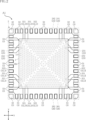
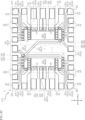
- FIG. 1 is a perspective view showing the electronic device according to the first embodiment, and shows a state seen from the bottom side.
- FIG. 2 is a plan view showing the electronic device according to the first embodiment, showing a resin member with imaginary lines.
- FIG. 3 is a diagram showing electronic components and a plurality of bonding layers in imaginary lines in the plan view of FIG. 2 .
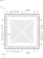
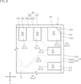
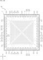
- FIG. 4 is a bottom view of the electronic device according to the first embodiment;
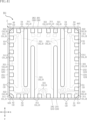
- FIG. 5 is a partial enlarged view enlarging a portion of FIG. 4 (near the first corner terminal).
- FIG. 6 is a partially enlarged view enlarging a part of FIG. 4 (near the second corner terminal).
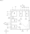
- FIG. 7 is a partial enlarged view enlarging a part of FIG.
- FIG. 8 is a partially enlarged view enlarging a portion of FIG. 4 (near the fourth corner terminal).
- 9 is a front view of the electronic device according to the first embodiment;
- FIG. 10 is a rear view of the electronic device according to the first embodiment;
- FIG. 11 is a right side view of the electronic device according to the first embodiment;
- FIG. 12 is a left side view of the electronic device according to the first embodiment;
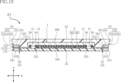
- FIG. 15 is a cross-sectional view along line XV-XV in FIG. 3.
- FIG. 16 is a cross-sectional view taken along line XVI--XVI of FIG. 3.
- FIG. 20 is a cross-sectional view showing one step of the method for manufacturing the electronic device according to the first embodiment;
- FIG. 21 is a cross-sectional view showing one step of the method for manufacturing the electronic device according to the first embodiment;
- FIG. 17 is a cross-sectional view showing one step of the method for manufacturing the electronic device according to the first embodiment;
- 18 is a cross-sectional view showing one step of the method for manufacturing the electronic device according to the first embodiment;
- FIG. 19 is a cross-sectional view showing one step of the method for manufacturing the electronic device
- FIG. 22 is a cross-sectional view showing one step of the method for manufacturing the electronic device according to the first embodiment
- FIG. 23 is a cross-sectional view showing one step of the method for manufacturing the electronic device according to the first embodiment
- FIG. FIG. 24 is a bottom view of a main part showing one step of the method of manufacturing the electronic device according to the first embodiment
- 25 is a cross-sectional view showing one step of the method for manufacturing the electronic device according to the first embodiment
- FIG. 26 is a bottom view of a main part showing one step of the method of manufacturing the electronic device according to the first embodiment
- FIG. 27 is a cross-sectional view showing one step of the method for manufacturing the electronic device according to the first embodiment
- FIG. 24 is a bottom view of a main part showing one step of the method of manufacturing the electronic device according to the first embodiment
- 25 is a cross-sectional view showing one step of the method for manufacturing the electronic device according to the first embodiment
- FIG. 26 is a bottom view of a main part showing one step of the
- FIG. 28 is a bottom view of the electronic device according to the first modification of the first embodiment;
- FIG. 29 is a cross-sectional view showing an electronic device according to a first modification of the first embodiment, corresponding to the cross-section shown in FIG. 15.
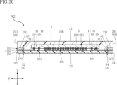
- FIG. 30 is a cross-sectional view showing an electronic device according to a first modification of the first embodiment, corresponding to the cross-section shown in FIG. 16.
- FIG. 31 is a cross-sectional view showing an electronic device according to a second modification of the first embodiment, corresponding to the cross-section shown in FIG. 13.
- FIG. 32 is a cross-sectional view showing an electronic device according to a third modification of the first embodiment, corresponding to the cross-section shown in FIG. 13.
- FIG. 33 is a cross-sectional view showing an electronic device according to a third modification of the first embodiment, corresponding to the cross-section shown in FIG. 15.
- FIG. FIG. 34 is a plan view showing the electronic device according to the fourth modification of the first embodiment, showing a resin member, an electronic component, and a plurality of bonding layers with imaginary lines.
- FIG. 35 is a partially enlarged view enlarging part of FIG. 34 (near the first corner terminal).
- 36 is a cross-sectional view taken along line XXXVI-XXXVI of FIG. 35.
- FIG. 37 is an enlarged view of a main part showing another configuration example of the electronic device according to the fourth modification of the first embodiment;
- FIG. 37 is an enlarged view of a main part showing another configuration example of the electronic device according to the fourth modification of the first embodiment; FIG.
- FIG. 38 is a bottom view of the electronic device according to the fifth modification of the first embodiment;
- FIG. FIG. 39 is a plan view showing the electronic device according to the second embodiment, showing a resin member with imaginary lines.
- FIG. 40 is a diagram showing the electronic components in imaginary lines in the plan view of FIG. 39 .
- FIG. 41 is a bottom view of the electronic device according to the second embodiment;
- FIG. 42 is a plan view showing the electronic device according to the third embodiment, and shows the resin members with imaginary lines.
- a certain entity A is formed on a certain entity B
- a certain entity A is formed on (of) an entity B
- mean a certain entity A is directly formed in a certain thing B
- a certain thing A is formed in a certain thing B while another thing is interposed between a certain thing A and a certain thing B” including.
- ⁇ an entity A is arranged on an entity B'' and ⁇ an entity A is arranged on (of) an entity B'' mean ⁇ an entity A being placed directly on a certain thing B", and "a thing A being placed on a certain thing B with another thing interposed between something A and something B" include.
- ⁇ an object A is located on (of) an object B'' means ⁇ a certain object A is in contact with an object B, and an object A is located on an object B. Being located on (of)" and "something A is located on (something) B while another thing is interposed between something A and something B including "things”.
- ⁇ a certain object A overlaps an object B when viewed in a certain direction'' means ⁇ a certain object A overlaps all of an object B'', and ⁇ a certain object A overlaps an object B.'' It includes "overlapping a part of a certain thing B".
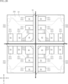
- First embodiment: 1 to 16 show an electronic device A1 according to the first embodiment.
- An electronic device A1 includes an electronic component 1, a resin member 2, and a conductive member 3. As shown in FIG.
- the thickness direction of the electronic device A1 (resin member 2) will be referred to as "thickness direction z".
- thickness direction z the thickness direction of the electronic device A1 (resin member 2)
- descriptions such as “upper”, “lower”, “upper”, “lower”, “upper surface” and “lower surface” indicate the relative positional relationship of each part, part, etc. in the thickness direction z. and is not necessarily a term that defines the relationship with the direction of gravity.
- plane view refers to the time when viewed in the thickness direction z.
- a direction orthogonal to the thickness direction z is called a "first direction x”
- a direction orthogonal to the thickness direction z and the first direction x is called a "second direction y”.
- the first direction x is the horizontal direction in the plan view of the electronic device A1 (see FIGS. 2 and 3)
- the second direction y is the plan view of the electronic device A1 (see FIGS. 2 and 3). Up-down direction.
- the electronic device A1 is a surface mount type package. As shown in FIG. 1, the package structure of the electronic device A1 is, for example, a MAP type QFN. The electronic device A1 has, for example, a rectangular shape in plan view, as shown in FIGS.
- the electronic component 1 is an element that exhibits the electrical functions of the electronic device A1.
- Electronic component 1 has, for example, a rectangular shape in plan view.
- the electronic component 1 is, for example, a semiconductor element containing a semiconductor material.
- an integrated circuit element is adopted as an example of a semiconductor element.
- the electronic component 1 may be an active functional element (such as a transistor or diode) or a passive functional element (such as a resistor, capacitor or inductor) or the like, rather than an integrated circuit element.
- the electronic component 1 has an element main surface 10a and an element back surface 10b.
- the element main surface 10a and the element back surface 10b are spaced apart in the thickness direction z and face opposite sides.
- the element main surface 10a faces downward in the thickness direction z, and the element rear surface 10b faces upward in the thickness direction.
- the electronic component 1 is flip-chip mounted on the conductive member 3, and the main surface 10a of the element faces the conductive member 3 as shown in FIGS.
- the electronic component 1 has a plurality of electrodes 11 arranged on the main surface 10a of the element.
- the number, arrangement, shape and planar view size of the plurality of electrodes 11 are not limited to the illustrated example, and may be changed as appropriate according to the electronic component 1 used.
- the multiple electrodes 11 are bonded to the conductive member 3 via multiple bonding layers 19 .
- Bonding layer 19 is formed of a metal laminate, for example, in which an Sn layer is laminated on a Ni layer, and an Ag layer is further laminated on the Sn layer.
- the bonding layer 19 may be a conductive bonding material such as solder, sintered metal, or metal paste instead of this metal laminate.
- the resin member 2 is a sealing material that protects the electronic component 1.
- the resin member 2 is made of an insulating resin material.
- the resin material is, for example, black epoxy resin.
- the resin member 2 covers part of the conductive member 3 and the electronic component 1.
- the resin member 2 has a rectangular shape in plan view.
- the resin member 2 has a resin main surface 21 , a resin back surface 22 , a first resin side surface 23 , a second resin side surface 24 , a third resin side surface 25 and a fourth resin side surface 26 .
- the first resin side surface 23 and the third resin side surface 25 are separated in the first direction x as shown in FIGS. 2 to 4, 9, 10 and 15.
- FIG. The first resin side surface 23 and the third resin side surface 25 are connected to both the resin main surface 21 and the resin back surface 22 and are sandwiched between them in the thickness direction z.
- the first resin side surface 23 intersects with each of the second resin side surface 24 and the fourth resin side surface 26, as shown in FIGS.
- the first resin side surface 23 is positioned on one side in the first direction x with respect to the electronic component 1 in plan view.
- the first resin side surface 23 has a first side end surface 231 and a first resin recess 232. As shown in FIGS.
- the first side end surface 231 faces one side of the first direction x, as shown in FIGS. 9, 10 and 15 .
- the first side end surface 231 is flat.
- the first side end surface 231 forms part of the outer periphery of the resin member 2 in plan view.
- the first resin concave portion 232 is recessed from the first side end face 231 and connected to the resin back surface 22.
- the first resin recess 232 has a first wall surface 232a and a first bottom surface 232b.
- the first wall surface 232 a faces the same direction as the first side end surface 231 .
- the first wall surface 232a is located in the other direction x than the first side end surface 231, that is, in a plan view from the first side end surface 231. It is located inside the electronic device A1.
- the first bottom surface 232b connects to the first side end surface 231 and the first wall surface 232a.
- the first bottom surface 232b is flat and faces downward in the thickness direction z. Unlike this example, the first bottom surface 232b may be curved concavely.
- the third resin side surface 25 intersects with each of the second resin side surface 24 and the fourth resin side surface 26, as shown in FIGS.
- the third resin side surface 25 is connected to the edge of each of the second resin side surface 24 and the fourth resin side surface 26 opposite to the side connected to the first resin side surface 23 in the first direction x.
- the third resin side surface 25 is located on the other side of the first direction x with respect to the electronic component 1 in plan view.
- the third resin side surface 25 has a third side end surface 251 and a third resin concave portion 252 as shown in FIGS. 9, 10 and 15 .
- the third side end face 251 faces the other of the first direction x, as shown in FIGS.
- the third side end surface 251 is flat.
- the third side end surface 251 forms part of the outer periphery of the resin member 2 in plan view.
- the third resin concave portion 252 is recessed from the third side end surface 251 and connected to the resin back surface 22.
- the third resin recess 252 has a third wall surface 252a and a third bottom surface 252b.
- the third wall surface 252 a faces the same direction as the third side end surface 251 .
- the third wall surface 252a extends in the first direction x from the third side end surface 251, that is, from the third side end surface 251. It is positioned inside the electronic device A1 in plan view.
- the third bottom surface 252b connects to the third side end surface 251 and the third wall surface 252a.
- the third bottom surface 252b is flat and faces downward in the thickness direction z. Unlike this example, the third bottom surface 252b may be curved concavely.
- the second resin side surface 24 and the fourth resin side surface 26 are spaced apart in the second direction y as shown in FIGS.
- the second resin side surface 24 and the fourth resin side surface 26 are connected to both the resin main surface 21 and the resin back surface 22 and are sandwiched between them in the thickness direction z.
- the second resin side surface 24 intersects with each of the first resin side surface 23 and the third resin side surface 25, as shown in FIGS.
- the second resin side surface 24 is positioned on one side in the second direction y with respect to the electronic component 1 in plan view.
- the second resin side surface 24 has a second side end surface 241 and a second resin recess 242. As shown in FIGS.
- the second side end surface 241 faces one side of the second direction y, as shown in FIGS.
- the second side end face 241 is flat.
- the second side end surface 241 forms part of the outer periphery of the resin member 2 in plan view.
- the second resin concave portion 242 is recessed from the second side end surface 241 and connected to the resin back surface 22.
- the second resin recess 242 has a second wall surface 242a and a second bottom surface 242b.
- the second wall surface 242 a faces the same direction as the second side end surface 241 .
- the second wall surface 242a extends further in the second direction y than the second side end surface 241, that is, the second side surface 241. It is positioned inside the electronic device A1 in plan view.
- the second bottom surface 242b connects to the second side end surface 241 and the second wall surface 242a.
- the second bottom surface 242b is flat and faces downward in the thickness direction z. Unlike this example, the second bottom surface 242b may be curved concavely.
- the fourth resin side surface 26 intersects with each of the first resin side surface 23 and the third resin side surface 25, as shown in FIGS.
- the fourth resin side surface 26 is connected to the edge of each of the first resin side surface 23 and the third resin side surface 25 on the side opposite to the side connected to the second resin side surface 24 in the second direction y.
- the fourth resin side surface 26 is positioned on the other side in the second direction y with respect to the electronic component 1 in plan view.
- the fourth resin side surface 26 has a fourth side end surface 261 and a fourth resin concave portion 262 as shown in FIGS. 11, 12 and 16 .
- the fourth side end face 261 faces the other side of the second direction y, as shown in FIGS.
- the fourth side end surface 261 is flat.
- the fourth side end surface 261 forms part of the outer periphery of the resin member 2 in plan view.
- the fourth resin concave portion 262 is recessed from the fourth side end surface 261 and connected to the resin rear surface 22.
- the fourth resin recess 262 has a fourth wall surface 262a and a fourth bottom surface 262b.
- the fourth wall surface 262 a faces the same direction as the fourth side end surface 261 .
- the fourth wall surface 262a is located in the second direction y relative to the fourth side end surface 261, that is, the fourth side surface 261. It is positioned inside the electronic device A1 in plan view.
- the fourth bottom surface 262b connects to the fourth side end surface 261 and the fourth wall surface 262a.
- the fourth bottom surface 262b is flat and faces downward in the thickness direction z. Unlike this example, the fourth bottom surface 262b may be curved concavely.
- the resin member 2 includes a first resin portion 201 and a second resin portion 202.
- the first resin portion 201 and the second resin portion 202 are laminated in the thickness direction z and are in contact with each other.
- the first resin portion 201 and the second resin portion 202 are obtained by dividing the resin member 2, and are limited to those in which the boundary between the first resin portion 201 and the second resin portion 202 can be visually recognized.
- a mode in which the first resin portion 201 and the second resin portion 202 are integrated is also included.
- the first resin portion 201 is located below the second resin portion 202 in the thickness direction z.
- the lower surface of the first resin portion 201 (the surface facing downward in the thickness direction z) is the resin back surface 22 . Therefore, the first resin portion 201 has a resin rear surface 22 .
- the upper surface of the second resin portion 202 (the surface facing upward in the thickness direction z) is the main resin surface 21 . Therefore, the second resin portion 202 has a resin main surface 21 .
- the upper surface of the first resin portion 201 (the surface facing upward in the thickness direction z) and the lower surface of the second resin portion 202 (the surface facing downward in the thickness direction z) are in contact with each other.
- the conductive member 3 conducts to the electronic component 1 as appropriate.
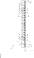
- the conductive member 3 includes a first conductor layer 31, a second conductor layer 32 and a third conductor layer 33, as shown in FIGS. 2-8 and 13-16.
- the first conductor layer 31 penetrates the first resin portion 201 in the thickness direction z, as shown in FIGS. As shown in FIGS. 13 to 16, the first conductor layer 31 is exposed from the resin rear surface 22 and is formed on any one of the first resin side surface 23, the second resin side surface 24, the third resin side surface 25 and the fourth resin side surface 26. exposed from the heel.
- a constituent material of the first conductor layer 31 is, for example, copper or a copper alloy.
- the first conductor layer 31 includes a plurality of columnar portions 311 spaced apart from each other.
- the plurality of columnar portions 311 are prismatic, for example, and rectangular in plan view as shown in FIG. 4 . In this embodiment, each columnar portion 311 is partially exposed from the resin member 2 .
- the second conductor layer 32 is formed on the first conductor layer 31 or the first resin portion 201, as shown in FIGS.
- the second conductor layer 32 is pattern wiring.
- the constituent material of the second conductor layer 32 is, for example, copper or a copper alloy.
- the second conductor layer 32 is electrically connected to the first conductor layer 31 .
- the second conductor layer 32 includes a plurality of wiring portions 321 and a plurality of intervening portions 322, as shown in FIG.
- Each of the plurality of wiring portions 321 is a portion of the second conductor layer 32 that is electrically connected to the electronic component 1 .
- the bonding layer 19 is formed on each wiring portion 321 .
- Each of the plurality of intervening portions 322 is a portion of the second conductor layer 32 that does not conduct to the electronic component 1 .
- the multiple interposed portions 322 are sandwiched between the first conductor layer 31 and the third conductor layer 33 in the thickness direction z.
- the third conductor layer 33 is formed on the second conductor layer 32, as shown in FIGS.
- the third conductor layer 33 is partially covered with the second resin portion 202 .
- the third conductor layer 33 is exposed from any one of the first resin side surface 23 , the second resin side surface 24 , the third resin side surface 25 and the fourth resin side surface 26 .
- a constituent material of the third conductor layer 33 is, for example, copper or a copper alloy.
- the third conductor layer 33 includes a plurality of columnar portions 331 spaced apart from each other.
- the plurality of columnar portions 331 are, for example, prismatic and, as shown in FIG. 3, rectangular in plan view. In this embodiment, each columnar portion 331 is partially exposed from the resin member 2 . As understood from FIGS. 2 to 4, each of the plurality of columnar portions 331 overlaps one of the plurality of columnar portions 311 in plan view.
- the conductive member 3 includes a first corner terminal 41, a second corner terminal 42, a third corner terminal 43, a fourth corner terminal 44, a plurality of first lateral terminals 51, a plurality of It includes a second side terminal 52 , a plurality of third side terminals 53 and a plurality of fourth side terminals 54 .
- a first corner terminal 41 , a second corner terminal 42 , a third corner terminal 43 , a fourth corner terminal 44 , a plurality of first lateral terminals 51 , a plurality of second lateral terminals 52 , a plurality of third lateral terminals 53 and the plurality of fourth side terminals 54 are partially exposed from the resin member 2 .
- a first corner terminal 41 , a second corner terminal 42 , a third corner terminal 43 , a fourth corner terminal 44 , a plurality of first lateral terminals 51 , a plurality of second lateral terminals 52 , a plurality of third lateral terminals 53 and some of the plurality of fourth side terminals 54 are electrically connected to the electronic component 1 .
- a first corner terminal 41 , a second corner terminal 42 , a third corner terminal 43 , a fourth corner terminal 44 , a plurality of first lateral terminals 51 , a plurality of second lateral terminals 52 , a plurality of third lateral terminals 53 and the plurality of fourth side terminals 54 are respectively used when mounting the electronic device A1 on a circuit board of an electronic device or the like.
- the first corner terminal 41, the second corner terminal 42, the third corner terminal 43 and the fourth corner terminal 44 are arranged near four corners of the resin member 2 in plan view. In this embodiment, none of the first corner terminal 41 , the second corner terminal 42 , the third corner terminal 43 and the fourth corner terminal 44 are electrically connected to the electronic component 1 .
- the first square terminal 41 is exposed from the resin rear surface 22 and also exposed from the first resin side surface 23 and the second resin side surface 24.
- the first square terminal 41 includes a columnar portion 311 of the first conductor layer 31 , an intermediate portion 322 of the second conductor layer 32 and a columnar portion 331 of the third conductor layer 33 .
- the columnar portion 311 forming the first corner terminal 41 is an example of the "first columnar portion”
- the columnar portion 331 forming the first corner terminal 41 is an example of the "second columnar portion”.
- the first corner terminal 41 has a first exposed surface 411, a second exposed surface 412, a first surface 413 and a rear surface 414, as shown in FIG.
- the first exposed surface 411 is exposed from the first resin side surface 23.
- the first exposed surface 411 is exposed in the first resin recessed portion 232 of the first resin side surface 23 .
- the first exposed surface 411 faces one side in the first direction x.
- the first exposed surface 411 is flat.
- the first exposed surface 411 is flush with the first wall surface 232 a of the first resin recess 232 .
- the term “flush” means not only a mode in which two or more surfaces are ideally smooth surfaces, but also during processing in the manufacturing process of the electronic device A1 (for example, This includes the case where unevenness is inevitably formed during grinding and dicing (to be described later), and the case where processing marks are formed across the respective surfaces.
- the second exposed surface 412 is exposed from the second resin side surface 24.
- the second exposed surface 412 is exposed at the second resin recessed portion 242 of the second resin side surface 24 .
- the second exposed surface 412 faces one side in the second direction y.
- the second exposed surface 412 is flat.
- the second exposed surface 412 is flush with the second wall surface 242 a of the second resin recess 242 .
- the first surface 413 is connected to both the first exposed surface 411 and the second exposed surface 412 in plan view.
- the first surface 413 is covered with the resin member 2 .
- first surface 413 is flat and slopes with respect to each of first exposed surface 411 and second exposed surface 412 .
- the first surface 413 may be curved to be concave or convex in plan view.
- the back surface 414 faces downward in the thickness direction z.
- the back surface 414 is exposed from the resin back surface 22 as shown in FIG.
- Back surface 414 is flat.
- the back surface 414 is flush with the resin back surface 22 .
- the first square terminal 41 further has a covering surface 419 .
- the covering surface 419 is formed on the side opposite to the first surface 413 .
- Cover surface 419 is covered with resin member 2 .
- Cover surface 419 is flat.
- Covering surface 419 is formed, for example, on columnar portion 311 of first corner terminal 41 , and is not formed on intervening portion 322 and columnar portion 331 of first corner terminal 41 .
- the covering surface 419 may be formed across the columnar portion 311 of the first square terminal 41 and the intermediate portion 322 , or further across the columnar portion 331 .
- the covering surface 419 is provided on the first corner terminal 41 as a mark indicating the orientation of the electronic device A1.
- the covering surface 419 is not the first corner terminal 41 , but the second corner terminal 42 , the third corner terminal 43 , the fourth corner terminal 44 , the plurality of first side terminals 51 , and the plurality of second side terminals 52 . , the plurality of third side terminals 53 and the plurality of fourth side terminals 54 .
- the second corner terminals 42 are exposed from the resin rear surface 22 and also exposed from the second resin side surface 24 and the third resin side surface 25 respectively.
- the second corner terminal 42 includes a columnar portion 311 of the first conductor layer 31 , an intermediate portion 322 of the second conductor layer 32 and a columnar portion 331 of the third conductor layer 33 .
- the second corner terminal 42 has a third exposed surface 421, a fourth exposed surface 422, a second surface 423 and a rear surface 424, as shown in FIG.
- the third exposed surface 421 is exposed from the second resin side surface 24.
- the third exposed surface 421 is exposed at the second resin recessed portion 242 of the second resin side surface 24 .
- the third exposed surface 421 faces one side in the second direction y.
- the third exposed surface 421 is flat.
- the third exposed surface 421 is flush with the second wall surface 242 a of the second resin recess 242 .
- the fourth exposed surface 422 is exposed from the third resin side surface 25.
- the fourth exposed surface 422 is exposed in the third resin recessed portion 252 of the third resin side surface 25 .
- the fourth exposed surface 422 faces the other side of the first direction x.
- the fourth exposed surface 422 is flat.
- the fourth exposed surface 422 is flush with the third wall surface 252 a of the third resin recess 252 .
- the second surface 423 is connected to both the third exposed surface 421 and the fourth exposed surface 422 in plan view.
- the second surface 423 is covered with the resin member 2 .
- the second surface 423 is flat and slopes with respect to each of the third exposed surface 421 and the fourth exposed surface 422 .
- the second surface 423 may be curved such that it is concave in plan view or convex in plan view.
- the back surface 424 faces downward in the thickness direction z.
- the back surface 424 is exposed from the resin back surface 22 as shown in FIG.
- Back surface 424 is flat.
- the back surface 424 is flush with the resin back surface 22 .
- the third corner terminal 43 is exposed from the resin rear surface 22 and is also exposed from the third resin side surface 25 and the fourth resin side surface 26 respectively.
- the third corner terminal 43 includes a columnar portion 311 of the first conductor layer 31 , an intermediate portion 322 of the second conductor layer 32 and a columnar portion 331 of the third conductor layer 33 .
- the third corner terminal 43 has a fifth exposed surface 431 , a sixth exposed surface 432 , a third surface 433 and a rear surface 434 .
- the fifth exposed surface 431 is exposed from the third resin side surface 25.
- the fifth exposed surface 431 is exposed in the third resin recessed portion 252 of the third resin side surface 25 .
- the fifth exposed surface 431 faces the other side of the first direction x.
- the fifth exposed surface 431 is flat.
- the fifth exposed surface 431 is flush with the third wall surface 252 a of the third resin recess 252 .
- the sixth exposed surface 432 is exposed from the fourth resin side surface 26.
- the sixth exposed surface 432 is exposed at the fourth resin recessed portion 262 of the fourth resin side surface 26 .
- the sixth exposed surface 432 faces the other side of the second direction y.
- the sixth exposed surface 432 is flat.
- the sixth exposed surface 432 is flush with the fourth wall surface 262 a of the fourth resin recess 262 .
- the third surface 433 is connected to both the fifth exposed surface 431 and the sixth exposed surface 432 in plan view.
- the third surface 433 is covered with the resin member 2 .
- the third surface 433 is flat and slopes with respect to each of the fifth exposed surface 431 and the sixth exposed surface 432 .
- the third surface 433 may be curved so as to be concave or convex in plan view.
- the back surface 434 faces downward in the thickness direction z.
- the back surface 434 is exposed from the resin back surface 22 as shown in FIG.
- Back surface 434 is flat.
- the back surface 434 is flush with the resin back surface 22 .
- the fourth corner terminal 44 is exposed from the resin back surface 22 and also exposed from the fourth resin side surface 26 and the first resin side surface 23 .
- the fourth corner terminal 44 includes a columnar portion 311 of the first conductor layer 31 , an intermediate portion 322 of the second conductor layer 32 and a columnar portion 331 of the third conductor layer 33 .
- the fourth corner terminal 44 has a seventh exposed surface 441 , an eighth exposed surface 442 , a fourth surface 443 and a rear surface 444 .
- the seventh exposed surface 441 is exposed from the fourth resin side surface 26.
- the seventh exposed surface 441 is exposed in the fourth resin recessed portion 262 of the fourth resin side surface 26 .
- the seventh exposed surface 441 faces the other side of the second direction y.
- the seventh exposed surface 441 is flat.
- the seventh exposed surface 441 is flush with the fourth wall surface 262 a of the fourth resin recess 262 .
- the eighth exposed surface 442 is exposed from the first resin side surface 23.
- the eighth exposed surface 442 is exposed in the first resin recessed portion 232 of the first resin side surface 23 .
- the eighth exposed surface 442 faces one side in the first direction x.
- the eighth exposed surface 442 is flat.
- the eighth exposed surface 442 is flush with the first wall surface 232 a of the first resin recess 232 .
- the fourth surface 443 is connected to both the seventh exposed surface 441 and the eighth exposed surface 442 in plan view.
- the fourth surface 443 is covered with the resin member 2 .
- the fourth surface 443 is flat and slopes with respect to each of the seventh exposed surface 441 and the eighth exposed surface 442 .
- the fourth surface 443 may be curved so as to be concave or convex in plan view.
- the back surface 444 faces downward in the thickness direction z.
- the back surface 444 is exposed from the resin back surface 22 as shown in FIG.
- Back surface 444 is flat.
- the back surface 444 is flush with the resin back surface 22 .
- the fifth exposed surface 431, the sixth exposed surface 432 and the rear surface 434, and the seventh exposed surface 441, the eighth exposed surface 442 and the rear surface 444 of the fourth corner terminal 44 are each covered with a plating layer (not shown).
- the plating layer is formed to improve the wettability of solder.
- the solder is used, for example, when mounting the electronic device A1 on a circuit board of an electronic device or the like.
- the plated layer includes, for example, a Ni layer, a Pd layer and an Au layer formed by electroless plating, which will be described later.
- the constituent material of the plated layer is not limited to this.
- the plurality of first side terminals 51 are arranged along the first resin side surface 23, as shown in FIGS. Therefore, the plurality of first side terminals 51 are arranged in the second direction y.
- the plurality of first side terminals 51 are sandwiched between the first corner terminal 41 and the second corner terminal 42 in the second direction y and positioned between the first corner terminal 41 and the second corner terminal 42 .
- the plurality of first side terminals 51 are exposed from the first resin side surface 23 while being exposed from the resin back surface 22 . Some of the plurality of first side terminals 51 are electrically connected to the electronic component 1 and some are not electrically connected to the electronic component 1 .
- those that are electrically connected to the electronic component 1 include each columnar portion 311 , each wiring portion 321 and each columnar portion 331 .
- those that are not electrically connected to the electronic component 1 are configured to include each columnar portion 311 , each intermediate portion 322 and each columnar portion 331 .
- Each of the plurality of first side terminals 51 includes an exposed surface 511 and a back surface 512, as shown in FIGS. Each of the plurality of first side terminals 51 is covered with the resin member 2 on the surfaces other than the exposed surface 511 and the back surface 512 .
- each first side terminal 51 is exposed from the first resin side surface 23 .
- the exposed surface 511 is exposed in the first resin recessed portion 232 of the first resin side surface 23 .
- the exposed surface 511 is flat.
- the exposed surface 511 is flush with the first wall surface 232 a of the first resin recess 232 .
- each first side terminal 51 the rear surface 512 is exposed from the resin rear surface 22, as shown in FIGS.
- the back surface 512 is flush with the resin back surface 22 .
- the back surface 512 connects to the exposed surface 511 .
- the plurality of second side terminals 52 are arranged along the second resin side surface 24, as shown in FIGS. Therefore, the plurality of second side terminals 52 are arranged in the first direction x.
- the plurality of second side terminals 52 are sandwiched between the first corner terminal 41 and the second corner terminal 42 in the first direction x and positioned between the first corner terminal 41 and the second corner terminal 42 .
- the plurality of second side terminals 52 are exposed from the second resin side surface 24 while being exposed from the resin back surface 22 . Some of the plurality of second side terminals 52 are electrically connected to the electronic component 1 and some are not electrically connected to the electronic component 1 .
- those that are electrically connected to the electronic component 1 include each columnar portion 311 , each wiring portion 321 and each columnar portion 331 .
- those that are not electrically connected to the electronic component 1 are configured to include each columnar portion 311 , each intermediate portion 322 and each columnar portion 331 .
- Each of the plurality of second side terminals 52 includes an exposed surface 521 and a rear surface 522, as shown in FIGS. Each of the plurality of second side terminals 52 is covered with the resin member 2 on the surfaces other than the exposed surface 521 and the back surface 522 .
- each second side terminal 52 is exposed from the second resin side surface 24 .
- the exposed surface 521 is exposed in the second resin recessed portion 242 of the second resin side surface 24 .
- the exposed surface 521 is flat.
- the exposed surface 521 is flush with the second wall surface 242 a of the second resin recess 242 .
- each second side terminal 52 the rear surface 522 is exposed from the resin rear surface 22, as shown in FIGS.
- the back surface 522 is flush with the resin back surface 22 .
- the back surface 522 connects to the exposed surface 521 .
- the plurality of third side terminals 53 are arranged along the third resin side surface 25, as shown in FIGS. Therefore, the plurality of third side terminals 53 are arranged in the second direction y.
- the plurality of third side terminals 53 are sandwiched between the second corner terminal 42 and the third corner terminal 43 and positioned between the second corner terminal 42 and the third corner terminal 43 in the second direction y.
- the plurality of third side terminals 53 are exposed from the third resin side surface 25 while being exposed from the resin back surface 22 .
- Some of the plurality of third side terminals 53 are electrically connected to the electronic component 1 and some are not electrically connected to the electronic component 1 .
- those that are electrically connected to the electronic component 1 include each columnar portion 311 , each wiring portion 321 and each columnar portion 331 .
- those that are not electrically connected to the electronic component 1 include each columnar portion 311 , each intermediate portion 322 and each columnar portion 331 .
- Each of the plurality of third side terminals 53 includes an exposed surface 531 and a rear surface 532, as shown in FIGS.
- the surfaces other than the exposed surface 531 and the back surface 532 of each of the plurality of third side terminals 53 are covered with the resin member 2 .
- each third side terminal 53 is exposed from the third resin side surface 25 .
- the exposed surface 531 is exposed in the third resin recessed portion 252 of the third resin side surface 25 .
- the exposed surface 531 is flat.
- the exposed surface 531 is flush with the third wall surface 252 a of the third resin recess 252 .
- each third side terminal 53 the back surface 532 is exposed from the resin back surface 22, as shown in FIGS.
- the back surface 532 is flush with the resin back surface 22 .
- the back surface 532 connects to the exposed surface 531 .
- the plurality of fourth side terminals 54 are arranged along the fourth resin side surface 26, as shown in FIGS. Therefore, the plurality of fourth side terminals 54 are arranged in the first direction x.
- the plurality of fourth side terminals 54 are sandwiched between the third corner terminal 43 and the fourth corner terminal 44 in the first direction x and positioned between the third corner terminal 43 and the fourth corner terminal 44 .
- the plurality of fourth side terminals 54 are exposed from the fourth resin side surface 26 while being exposed from the resin back surface 22 . Some of the plurality of fourth side terminals 54 are electrically connected to the electronic component 1 and some are not electrically connected to the electronic component 1 .
- those that are electrically connected to the electronic component 1 include each columnar portion 311 , each wiring portion 321 and each columnar portion 331 .
- those that are not electrically connected to the electronic component 1 are configured to include each columnar portion 311 , each intermediate portion 322 and each columnar portion 331 .
- Each of the plurality of fourth side terminals 54 includes an exposed surface 541 and a rear surface 542, as shown in FIGS. Each of the plurality of fourth side terminals 54 is covered with the resin member 2 on the surfaces other than the exposed surface 541 and the back surface 542 .
- each fourth side terminal 54 is exposed from the fourth resin side surface 26 .
- the exposed surface 541 is exposed in the fourth resin recessed portion 262 of the fourth resin side surface 26 .
- the exposed surface 541 is flat.
- the exposed surface 541 is flush with the fourth wall surface 262 a of the fourth resin recess 262 .
- each fourth side terminal 54 the rear surface 542 is exposed from the resin rear surface 22, as shown in FIGS.
- the back surface 542 is flush with the resin back surface 22 .
- the back surface 542 connects to the exposed surface 541 .
- the exposed surface 541 and the rear surface 542 of the 4-side terminal 54 are each covered with a plating layer (not shown).
- the plating layer is formed to improve the wettability of solder.
- the solder is used, for example, when mounting the electronic device A1 on a circuit board of an electronic device or the like.
- the plated layer includes, for example, a Ni layer, a Pd layer and an Au layer formed by electroless plating, which will be described later.
- the constituent material of the plated layer is not limited to this.
- FIG. 17 to 23, 25 and 27 are cross-sectional views showing one step of the method of manufacturing the electronic device A1, and correspond to the cross-section of the electronic device A1 shown in FIG. 24 and 26 are enlarged plan views of essential parts showing one step of the method of manufacturing the electronic device A1.
- each electronic device A1 in the process of being manufactured is arranged with its bottom facing upward in the thickness direction z. .
- a support substrate 90 is prepared, and the first conductor layer 31 is formed on the prepared support substrate 90 .
- a silicon substrate for example, is adopted as the support substrate 90 .
- the support substrate 90 may be a glass substrate instead of a silicon substrate.
- the support substrate 90 to be prepared has a size that allows a plurality of electronic devices A1 to be arranged vertically and horizontally in a matrix in plan view.
- a metal film made of copper or a copper alloy is formed by sputtering. Thereafter, a resist layer is patterned on the metal film by photolithography, and a plurality of metal columns made of copper or copper alloy are formed on the metal film exposed from the resist layer by electroplating. After removing the resist layer, the metal film exposed from the plurality of metal pillars is removed. Thereby, the first conductor layer 31 including the plurality of columnar portions 311 is formed.
- a first resin portion 201 is formed so as to cover the first conductor layer 31 formed on the support substrate 90.
- First resin portion 201 is an electrically insulating resin, and is made of, for example, epoxy resin or polyimide.
- the first resin portion 201 is formed by molding, for example.
- the first resin portion 201 is ground from the upper surface to expose the top surface of the first conductor layer 31 .
- the ground upper surface of the first resin portion 201 serves as a boundary with the second resin portion 202 to be formed later.
- a whetstone, for example, is used for grinding.
- the second conductor layer 32 , the plurality of bonding layers 19 and the third conductor layer 33 are formed on the top surface of the first resin portion 201 .
- the following five treatments first treatment to fifth treatment are performed.
- a seed layer is uniformly formed on the top surface of the first resin portion 201 .
- the seed layer is, for example, a metal thin film formed by sputtering.
- the metal thin film is made of, for example, nickel or chromium.
- a patterned resist layer is formed by photolithography on the seed layer formed in the first process, and copper or copper alloy is deposited by electroplating on the seed layer exposed from the resist layer. Thereby, the second conductor layer 32 connected by the seed layer is formed.
- a patterned resist layer is formed by photolithography on the second conductor layer 32 formed in the second process, and a Ni layer is formed by electroplating on the second conductor layer 32 exposed from the resist layer. , Sn layer and Ag layer are laminated in order. Then, the resist layer is removed. Thereby, a plurality of bonding layers 19 are formed.
- a patterned resist layer is formed by photolithography on the second conductor layer 32 formed in the second process, and the second conductor layer 32 exposed from the resist layer is electroplated with copper or copper. A plurality of metal columns made of a copper alloy are formed. Then, the resist layer is removed. Thereby, the third conductor layer 33 including the plurality of columnar portions 331 is formed.
- portions of the seed layer formed in the first process that are exposed from the second conductor layer 32, the plurality of bonding layers 19, and the third conductor layer 33 are removed.
- the second conductor layer 32 divided into a plurality of wiring portions 321 and a plurality of intervening portions 322 is formed from the second conductor layer 32 connected by the seed layer.
- the electronic component 1 is mounted on the second conductor layer 32 with the bonding layer 19 interposed therebetween.
- each electrode 11 arranged on the element main surface 10a is joined to the second conductor layer 32 via each bonding layer 19, and the element main surface 10a is in a posture facing the second conductor layer 32.
- An electronic component 1 is mounted. That is, the electronic component 1 is flip-chip mounted on the support substrate 90 via the first resin portion 201, the second conductor layer 32, the bonding layers 19, and the like.
- a second resin portion 202 is formed so as to cover the first resin portion 201, the second conductor layer 32, the third conductor layer 33, the plurality of bonding layers 19, and the electronic component 1.
- the second resin portion 202 is an electrically insulating resin, and is made of, for example, epoxy resin or polyimide.
- the second resin portion 202 is formed by molding, for example.
- the support substrate 90 is ground downward toward the second resin portion 202, and the support substrate 90 is removed. At this time, the grinding is performed until the first resin portion 201 has a predetermined thickness. This grinding exposes the bottom surface of each columnar portion 311 from the first resin portion 201 .
- FIGS. 24 and 25 half-cut dicing is performed to form grooves 91 having a lattice shape in plan view.
- 24 shows the state before half-cut dicing
- FIG. 25 shows the state after half-cut dicing.
- dots indicate areas to be half-cut diced.
- the dicing blade is moved in the direction indicated by the arrow shown in FIG. 24 (first dicing direction).
- first dicing direction In the first dicing direction along the first direction x, as shown in FIG. 24, the direction from the other side of the first direction x to the one side of the first direction x is the advancing direction of the dicing blade.
- the first dicing direction along the second direction y as shown in FIG.
- the direction from the other side of the second direction y to one side of the second direction y is the traveling direction of the dicing blade.
- half-cut diced regions are indicated by imaginary lines.
- first, the dicing blade is moved along the first dicing direction along the first direction x. This dicing is called "preceding first dicing".
- strip-shaped portions along the first direction x are formed in the grooves 91, and the strip-shaped portions along the first direction x have the second exposed surface 412, the third exposed surface 421, A sixth exposed surface 432 and a seventh exposed surface 441 are formed.
- the dicing blade is moved along the first dicing direction along the second direction y.
- This dicing is referred to as "second attack first dicing".
- second dicing a streak-like portion along the second direction y is formed in the groove 91, and the first exposed surface 411 and the fourth exposed surface 422 are formed in the streak-like portion along the second direction y. , a fifth exposed surface 431 and an eighth exposed surface 442 are formed.
- grooves 91 formed in half-cut dicing are formed by resin member 2 (first resin portion 201 and second resin portion 202), first conductor layer 31, second conductor layer 32 and third conductor layer 32. It straddles the conductor layer 33 .
- the surfaces of the first conductor layer 31, the second conductor layer 32, and the third conductor layer 33 exposed from the resin back surface 22 and the grooves 91 are plated.
- a Ni layer, a Pd layer and an Au layer are deposited in order by electroless plating.
- a plated layer composed of a Ni layer, a Pd layer and an Au layer is formed on the seventh exposed surface 441 , the eighth exposed surface 442 and the rear surface 444 .
- FIGS. 26 and 27 show the electronic components 1 individually separated by full-cut dicing (cutting).
- 26 shows the state before full-cut dicing
- FIG. 27 shows the state after full-cut dicing.
- dots indicate areas to be full-cut diced.
- the dicing blade is moved in the direction indicated by the arrow shown in FIG. 26 (second dicing direction).
- the second dicing direction along the first direction x as shown in FIG. 26
- the direction from the other side of the first direction x to the one side of the first direction x is the advancing direction of the dicing blade.
- the second dicing direction along the second direction y as shown in FIG.
- the direction from the other side of the second direction y to the one side of the second direction y is the traveling direction of the dicing blade.
- a dicing blade used in full-cut dicing is thinner than a dicing blade used in half-cut dicing.
- the phantom line indicates the full-cut diced region.
- the dicing blade is moved along the second dicing direction along the first direction x. This dicing is called "preceding second dicing".
- a second side end face 241 and a fourth side end face 261 are formed by the preceding second dicing.
- the dicing blade is moved along the second dicing direction along the second direction y. This dicing is called "second attack second dicing".
- the first side end surface 231 and the third side end surface 251 are formed by the second dicing performed later.
- the first corner terminal 41 has a first exposed surface 411, a second exposed surface 412 and a first surface 413.
- the first exposed surface 411 is exposed from the first resin side surface 23 and the second exposed surface 412 is exposed from the second resin side surface 24 .
- the first surface 413 is connected to the first exposed surface 411 and the second exposed surface 412 and covered with the resin member 2 .
- the first exposed surface 411 is formed during the preceding first dicing in half-cut dicing
- the second exposed surface 412 is formed during the subsequent first dicing in half-cut dicing.
- first dicing and subsequent dicing are performed.
- Each terminal end of the second dicing overlaps a corner portion where the first exposed surface 411 and the second exposed surface 412 are connected.
- the corner portion where the first exposed surface 411 and the second exposed surface 412 are connected is subjected to a total of two processing loads during dicing. Therefore, the impact and stress applied to the first square terminal 41 are increased, and the possibility that the first square terminal 41 is peeled off is increased.
- the first square terminal 41 has the first surface 413, and the first surface 413 is covered with the resin member 2.
- Each end portion of the time becomes the resin member 2 instead of the first square terminal 41 .
- impact and stress applied to the first square terminal 41 are suppressed. Therefore, in the electronic device A ⁇ b>1 , it is possible to prevent the first square terminal 41 from peeling off from the resin member 2 .
- the second corner terminal 42 has a second surface 423 connected to a third exposed surface 421 and a fourth exposed surface 422, and the third corner terminal 43 has a fifth exposed surface 431 and a sixth exposed surface. 432 , and the fourth corner terminal 44 has a fourth surface 443 connected to the seventh exposed surface 441 and the eighth exposed surface 442 .
- the second surface 423 , the third surface 433 and the fourth surface 443 are each covered with the resin member 2 . According to this configuration, in the electronic device A1, in addition to the first corner terminal 41, the second corner terminal 42, the third corner terminal 43, and the fourth corner terminal 44 can also be prevented from peeling off from the resin member 2.
- the terminals (the first corner terminal 41, the second corner terminal 42, the third corner terminal 43, and the fourth corner terminal 44) arranged near the four corners of the resin member 2 in plan view are respectively Separation from the resin member 2 can be suppressed.
- the first exposed surface 411, the second exposed surface 412, the third exposed surface 421, the fourth exposed surface 422, the fifth exposed surface 431, the sixth exposed surface 432, the seventh exposed surface 441, the eighth exposed surface A plating layer is formed on the surface 442, each exposed surface 511, each exposed surface 521, each exposed surface 531, and each exposed surface 541, respectively.
- a solder fillet is formed on the surface 442, each exposed surface 511, each exposed surface 521, each exposed surface 531, and each exposed surface 541, respectively.
- the first square terminal 41 includes a columnar portion 331. According to this configuration, the first square terminal 41 has a larger dimension along the thickness direction z than when the columnar portion 331 is not included. Thereby, the areas of the first exposed surface 411 and the second exposed surface 412 can be increased. The first exposed surface 411 and the second exposed surface 412 come into contact with a bonding material such as solder when the electronic device A1 is mounted on a circuit board such as an electronic device. In other words, since the contact area of the bonding material is increased, the electronic device A1 can increase the bonding strength to the circuit board of the electronic device or the like.
- the first square terminal 41 does not conduct to the electronic component 1.
- the first square terminal 41 that does not conduct to the electronic component 1 may not be provided in the electronic device A1 from an electrical point of view.
- the electronic device A1 includes the first corner terminals 41, it is possible to widen the bonding area by soldering or the like when mounting the electronic device A1 on a circuit board of an electronic device or the like.
- the first square terminal 41 allows the electronic device A1 to increase the mounting strength on a circuit board of an electronic device or the like. This is the same for the second corner terminal 42, the third corner terminal 43 and the fourth corner terminal 44 as well.
- the electronic device A2 differs from the electronic device A1 in the following points.
- the first resin side surface 23 of the electronic device A2 does not include the first resin recess 232 .
- the second resin side surface 24 of the electronic device A2 does not include the second resin recess 242 .
- the third resin side surface 25 of the electronic device A2 does not include the third resin recess 252 .
- the fourth resin side surface 26 of the electronic device A2 does not include the fourth resin recess 262 .
- the electronic device A2 shown in FIGS. 28 to 30 can be manufactured, for example, in the manufacturing method of the electronic device A1 without half-cut dicing.
- the back surface 414 of the first square terminal 41, the back surface 424 of the second square terminal 42, the back surface 434 of the third square terminal 43, and the back surface 434 of the third square terminal 43 are formed by the electroless plating.
- plating eg Ni, Pd and Au layers
- the first exposed surface 411 and the second exposed surface 412 are formed on the first corner terminal 41 by full-cut dicing. Further, by full-cut dicing, the second corner terminal 42 is formed with a third exposed surface 421 and a fourth exposed surface 422, the third corner terminal 43 is formed with a fifth exposed surface 431 and a sixth exposed surface 432, and the fourth corner terminal 44 is formed. A seventh exposed surface 441 and an eighth exposed surface 442 are respectively formed on the .
- the first corner terminal 41 has a first surface 413, the first surface 413 is connected to the first exposed surface 411 and the second exposed surface 412, and the resin member covered by 2. Therefore, in the electronic device A2, like the electronic device A1, the terminals exposed from the resin member 2 (the first corner terminals 41, etc.) can be prevented from peeling off. This is the same for the second corner terminal 42, the third corner terminal 43 and the fourth corner terminal 44 as well. It should be noted that the electronic device A2 achieves the same effects as the electronic device A1 due to the configuration common to the electronic device A1.
- FIG. 31 shows an electronic device A3 according to the second modification of the first embodiment.
- the electronic device A3 differs from the electronic device A1 in that the second conductor layer 32 does not include each intervening portion 322 .
- each of the first corner terminal 41 and the third corner terminal 43 has a columnar portion 331 formed on the columnar portion 311 and in contact with the columnar portion 311 .
- each of the second corner terminal 42 and the fourth corner terminal 44 also has a columnar portion 331 formed on the columnar portion 311 and in contact with the columnar portion 311 .
- those that are not electrically connected to the electronic component 1 are columnar.
- a portion 331 is formed on the columnar portion 311 and contacts the columnar portion 311 .
- the first corner terminal 41 has a first surface 413, the first surface 413 is connected to the first exposed surface 411 and the second exposed surface 412, and the resin member covered by 2. Therefore, in the electronic device A3, like the electronic device A1, the terminals exposed from the resin member 2 (the first corner terminal 41, etc.) can be prevented from peeling off. This is the same for the second corner terminal 42, the third corner terminal 43 and the fourth corner terminal 44 as well. It should be noted that the electronic device A3 achieves the same effects as the electronic devices A1 and A2 due to the configuration common to the electronic devices A1 and A2.
- FIG 32 and 33 show an electronic device A4 according to the third modified example of the first embodiment.
- the electronic device A4 differs from the electronic device A1 in that the third conductor layer 33 (each columnar portion 331) is not provided.
- the conductive member 3 does not include the third conductor layer 33, so as shown in FIG. is not formed.
- the second corner terminal 42 and the fourth corner terminal 44 also do not have the columnar portion 331 formed on the intervening portion 322 .
- each of the plurality of first side terminals 51, the plurality of second side terminals 52, the plurality of third side terminals 53, and the plurality of fourth side terminals 54 , the columnar portion 331 is not formed on the wiring portion 321 or the intervening portion 322 .
- the first corner terminal 41 has a first surface 413, the first surface 413 is connected to the first exposed surface 411 and the second exposed surface 412, and the resin member covered by 2. Therefore, in the electronic device A4, like the electronic device A1, the terminals exposed from the resin member 2 (the first corner terminals 41, etc.) can be prevented from peeling off. This is the same for the second corner terminal 42, the third corner terminal 43 and the fourth corner terminal 44 as well. However, for example, in the electronic device A ⁇ b>1 , the areas of the first exposed surface 411 and the second exposed surface 412 of the first square terminal 41 are increased by the columnar portions 331 .
- the electronic device A1 mounting strength on a circuit board of an electronic device or the like is enhanced.
- the improvement of the mounting strength by such a columnar portion 331 is achieved by the second corner terminal 42, the third corner terminal 43, the fourth corner terminal 44, the plurality of first side terminals 51, the plurality of second side terminals 52, the plurality of The same applies to each of the third side terminal 53 and the plurality of fourth side terminals 54 of .
- the electronic device A1 is preferable to the electronic device A4 in terms of improving the mounting strength. It should be noted that the electronic device A4 has the same effect as each of the electronic devices A1 to A3 due to the structure common to each of the electronic devices A1 to A3.
- 34 to 36 show an electronic device A5 according to the fourth modification of the first embodiment.
- the shapes of the columnar portions 331 of the first corner terminal 41, the second corner terminal 42, the third corner terminal 43, and the fourth corner terminal 44 are different from those of the electronic device A1.
- the columnar portion 331 of the first corner terminal 41 is divided into two parts. Therefore, the first corner terminal 41 further includes an exposed area 415 .
- the exposed area 415 is exposed from the columnar portion 331 of the first corner terminal 41 in plan view. In this embodiment, the exposed region 415 is part of the upper surface of the intervening portion 322 (the surface facing upward in the thickness direction z).
- the exposed region 415 is a part of the upper surface of the columnar portion 311 (the surface facing upward in the thickness direction z). is.
- the exposed region 415 overlaps the first surface 413 in plan view.
- the exposed region 415 extends in a direction orthogonal to the first surface 413 in plan view.
- the second corner terminal 42 further includes an exposed area 425, as shown in FIG.
- Third corner terminal 43 further includes an exposed area 435 .
- Fourth corner terminal 44 further includes an exposed area 445 .
- a dot is drawn in each exposed area 425, 435, 445.
- the exposed region 425 is exposed from the columnar portion 331 of the second corner terminal 42 in plan view.
- the exposed region 435 is exposed from the columnar portion 331 of the third corner terminal 43 in plan view.
- the exposed region 445 is exposed from the columnar portion 331 of the fourth corner terminal 44 in plan view.
- Each of the exposed regions 425, 435, 445 is configured similarly to the exposed region 415 in plan view.
- the first corner terminal 41 has a first surface 413, the first surface 413 is connected to the first exposed surface 411 and the second exposed surface 412, and the resin member covered by 2. Therefore, in the electronic device A5, like the electronic device A1, the terminals exposed from the resin member 2 (the first corner terminals 41, etc.) can be prevented from peeling off. This is the same for the second corner terminal 42, the third corner terminal 43 and the fourth corner terminal 44 as well. It should be noted that the electronic device A5 has the same effect as each of the electronic devices A1 to A4 due to the structure common to each of the electronic devices A1 to A4.
- the first corner terminal 41 has the columnar portion 331 divided into two parts and further includes an exposed area 415.
- resin member 2 is formed so as to be in contact with exposed region 415 .
- the electronic device A5 can increase the bonding strength between the resin member 2 and the first corner terminal 41 by the anchor effect.
- the electronic device A5 can further suppress peeling of the first corner terminal 41 compared to the electronic device A1. This is the same for the second corner terminal 42, the third corner terminal 43 and the fourth corner terminal 44 as well.
- FIG. 37 shows an example in which the columnar portion 331 of the first corner terminal 41 has a different shape from the example shown in the electronic device A5.
- the exposed region 415 includes a region along the first surface 413 in plan view.
- the electronic device shown in FIG. 37 also has the same effects as the electronic device A5.
- FIG. 38 shows an electronic device A6 according to the fifth modification of the first embodiment.
- the electronic device A6 differs from the electronic device A1 in the following points.
- First, the second corner terminal 42 of the electronic device A6 does not have the second surface 423 .
- Second, the third corner terminal 43 of the electronic device A6 does not have the third surface 433 .
- Thirdly, the fourth corner terminal 44 of the electronic device A6 does not have the fourth surface 443 .
- the first corner terminal 41 is cut after the second corner terminal 42, the third corner terminal 43, and the fourth corner terminal 44, for example, during half-cut dicing.
- the vibration and stress applied to the first corner terminal 41 during dicing are applied to the other second corner terminal 42, the third corner terminal 43, and the fourth corner terminal 44, respectively. and stress.
- the first surface 413 is provided only on the first corner terminals 41 that are highly likely to be peeled off.
- the first corner terminal 41 has a first surface 413, the first surface 413 is connected to the first exposed surface 411 and the second exposed surface 412, and the resin member covered by 2. Therefore, in the electronic device A6, like the electronic device A1, the terminals exposed from the resin member 2 (the first corner terminal 41, etc.) can be prevented from peeling off. It should be noted that the electronic device A6 has the same effect as each of the electronic devices A1 to A5 due to the structure common to each of the electronic devices A1 to A5.
- the first corner terminal 41 which is most likely to be separated from the resin member 2 is provided with the first surface 413.
- the second corner terminal 42 is provided with the second surface 423.
- the third corner terminal 43 may be provided with the third surface 433
- the fourth corner terminal 44 may be provided with the fourth surface 443 .
- two (or three) that are relatively likely to be peeled off from the resin member 2 are selected. select.
- the first corner terminal 41 and the fourth corner terminal 44 to be cut during the second dicing are two relatively high ones.
- any of the first surface 413, the second surface 423, the third surface 433, or the fourth surface 443 may then be formed on the selected one as appropriate. In other words, it is not necessary to form the first surface 413, the second surface 423, the third surface 433, or the fourth surface 443 on the part that is relatively unlikely to be peeled off from the resin member 2.
- Second embodiment 39 to 41 show an electronic device B1 according to the second embodiment.
- the electronic device B1 differs from the electronic device A1 in the following points.
- the electronic device B1 mainly differs in the configuration of the conductive member 3 .
- the first square terminal 41 is electrically connected to the electronic component 1, as shown in FIGS. Therefore, the first corner terminal 41 includes the wiring portion 321 instead of the intervening portion 322 compared to the first corner terminal 41 of the electronic device A1. Further, in the electronic device B1, as shown in FIGS. 39 to 41, the plurality of first side terminals 51, the plurality of second side terminals 52, the plurality of third side terminals 53 and the plurality of fourth side terminals All terminals 54 are electrically connected to the electronic component 1 .
- the first corner terminal 41 has the first face 413 as in the electronic device A1. According to this configuration, the electronic device B1 can suppress peeling of the first corner terminal 41 from the resin member 2 in the same manner as the electronic device A1. Further, in the electronic device B1, similarly to the electronic device A1, the second corner terminal 42 has the second surface 423, the third corner terminal 43 has the third surface 433, and the fourth corner terminal 44 has the fourth surface. It has a face 443 . Therefore, the electronic device B1 can suppress peeling of the second corner terminal 42, the third corner terminal 43, and the fourth corner terminal 44 from the resin member 2, similarly to the electronic device A1. Note that the electronic device B1 has the same effects as the electronic devices A1 to A6 due to the configuration common to the electronic devices A1 to A6.
- Third embodiment: 42 to 44 show an electronic device C1 according to the third embodiment.
- the electronic device C1 differs from the electronic devices A1 and B1 in the following points.
- First, the electronic device C1 comprises two electronic components 1 .
- two electronic components 1 are spaced apart in the first direction x, for example.
- a first corner terminal 41, a second corner terminal 42, a third corner terminal 43, a fourth corner terminal 44, a plurality of first lateral terminals 51, a plurality of Each of the second side terminal 52 , the plurality of third side terminals 53 and the plurality of fourth side terminals 54 is electrically connected to one of the two electronic components 1 .
- the second conductor layer 32 of the conductive member 3 does not include the intermediate portion 322, and the first corner terminal 41, the second corner terminal 42, the third corner terminal 43, the fourth corner terminal 44,
- the plurality of first side terminals 51 , the plurality of second side terminals 52 , the plurality of third side terminals 53 , and the plurality of fourth side terminals 54 each include the wiring portion 321 instead of the intervening portion 322 . Configured.
- the first conductor layer 31 of the conductive member 3 includes two plate-like portions 312. As shown in FIGS. The two plate-like portions 312 are arranged below the two electronic components 1 in the thickness direction z. One of the two plate-like portions 312 overlaps one of the two electronic components 1 in plan view, and the other of the two plate-like portions 312 overlaps the other of the two electronic components 1 in plan view. Each plate-like portion 312 functions as a radiator plate that radiates heat from each electronic component 1 . In addition, in the electronic device C ⁇ b>1 , each plate-like portion 312 may not be provided, and each plate-like portion 312 may be used as a terminal electrically connected to either one of the two electronic components 1 .
- the first corner terminal 41 has the first surface 413 as in the electronic device A1. According to this configuration, the electronic device C1 can suppress peeling of the first corner terminal 41 from the resin member 2 in the same manner as the electronic device A1. Further, in the electronic device C1, similarly to the electronic device A1, the second corner terminal 42 has the second surface 423, the third corner terminal 43 has the third surface 433, and the fourth corner terminal 44 has the fourth surface. It has a face 443 . Therefore, the electronic device C1 can suppress peeling of the second corner terminal 42, the third corner terminal 43, and the fourth corner terminal 44 from the resin member 2, similarly to the electronic device A1. Note that the electronic device C1 has the same effects as the electronic devices A1 to A6 and B1 due to the configuration common to the electronic devices A1 to A6 and B1.
- the electronic device of the present disclosure as can be understood from the electronic devices B1 and C1, all of the first corner terminal 41, the second corner terminal 42, the third corner terminal 43, and the fourth corner terminal 44 are Any one or more of the first corner terminal 41, the second corner terminal 42, the third corner terminal 43, and the fourth corner terminal 44 are configured to conduct to the electronic component 1. good too.
- the electronic device of the present disclosure is not limited to a configuration including one electronic component 1, and may be configured to include a plurality of electronic components 1.
- the configuration of the conductive member 3 is changed according to the type and number of electronic components 1 (types such as integrated circuit elements and discrete elements (including both active functional elements and passive functional elements)). It can be changed as appropriate.
- the configuration according to each modified example (second to fifth modified examples) of the first embodiment may be adopted as appropriate. That is, it is possible to apply the configuration of each of the electronic devices A2 to A6 to each of the electronic devices B1 and C1.
- the first resin side surface 23 may not include the first side end surface 231.
- the second conductor layer 32 may not include the intervening portions 322.
- the conductive member 3 may not include the third conductive layer 33, similarly to the electronic device A4.
- the first corner terminal 41, the second corner terminal 42, the third corner terminal 43, and the fourth corner terminal 44 each have an exposed region exposed from the columnar portion 331. 415, 425, 435, and 445 may be provided.
- the second corner terminal 42 does not have the second surface 423
- the third corner terminal 43 does not have the third surface 433
- the fourth corner terminal 44 does not have the fourth surface 443.
- the first square terminal 41 may be provided with the first surface 413 .
- the electronic component 1 is flip-mounted. However, unlike this configuration, the electronic component 1 may be mounted by bonding wires. In this configuration, the electronic component 1 is arranged with the back surface 10 b of the element facing the conductive member 3 . In addition, an island for bonding the electronic component 1 is appropriately provided on the conductive member 3 .
- the electronic device according to the present disclosure is not limited to the above-described embodiments.
- the specific configuration of each part of the electronic device of the present disclosure can be modified in various ways.
- the present disclosure includes the embodiments set forth in the Appendix below. Appendix 1.
- the resin member has a resin main surface and a resin back surface spaced apart in the thickness direction,
- Appendix 4. the resin member includes a first resin portion and a second resin portion that are laminated in the thickness direction and are in contact with each other; The first resin portion has the resin back surface, The electronic device according to Appendix 3, wherein the second resin portion has the resin main surface.
- the conductive member includes a first conductor layer penetrating the first resin portion in the thickness direction, 5.
- the electronic device according to appendix 4, wherein the first corner terminal includes a first columnar portion that is part of the first conductor layer. Appendix 6.
- the conductive member includes a second conductor layer sandwiched between the first resin portion and the second resin portion in the thickness direction, 6.
- the conductive member includes a third conductor layer formed on a side opposite to the first conductor layer with respect to the second conductor layer in the thickness direction, 7.
- Appendix 8. 8 The electronic device according to appendix 7, wherein the first corner terminal is a part of the second conductor layer and includes an intermediate portion sandwiched between the first columnar portion and the second columnar portion.
- the electronic device according to appendix 7 or appendix 8, wherein the first corner terminal has an exposed region exposed from the second columnar portion when viewed in the thickness direction.
- Appendix 10. The electronic device according to claim 9, wherein the exposed region is connected to the first surface when viewed in the thickness direction.
- Appendix 11. The electronic component has an element main surface and an element back surface that are spaced apart in the thickness direction, and has an electrode formed on the element main surface, the element main surface faces the second conductor layer, 11.
- the electronic device according to any one of appendices 6 to 10, wherein the electrode is joined to the second conductor layer.
- Appendix 12. the first resin side faces one side of a first direction perpendicular to the thickness direction; 12.
- the electronic device according to any one of attachments 3 to 11, wherein the second resin side surface faces one of second directions orthogonal to both the thickness direction and the first direction.
- Appendix 13 The resin member includes: a third resin side surface that intersects the second resin side surface and faces the opposite side of the first resin side surface in the first direction; having a fourth resin side surface facing the second resin side surface in two directions; 13.
- the electronic device according to appendix 12, wherein the third resin side surface and the fourth resin side surface intersect each other.
- Appendix 14 The resin member includes a first resin concave portion recessed from the resin back surface and connected to the first resin side surface, a second resin recess portion recessed from the resin back surface and connected to the second resin side surface, and a resin back surface recessed to the third resin side surface.
- the conductive member includes a second corner terminal, a third corner terminal, and a fourth corner terminal each exposed from the back surface of the resin; the second corner terminal has a third exposed surface exposed from the second resin side surface and a fourth exposed surface exposed from the third resin side surface; the third corner terminal has a fifth exposed surface exposed from the third resin side surface and a sixth exposed surface exposed from the fourth resin side surface; 15.
- the electronic device according to Appendix 13 or 14, wherein the fourth corner terminal has a seventh exposed surface exposed from the fourth resin side surface and an eighth exposed surface exposed from the first resin side surface.
- the second corner terminal has a second surface connected to both the third exposed surface and the fourth exposed surface when viewed in the thickness direction and covered with the resin member;
- the third corner terminal has a third surface connected to both the fifth exposed surface and the sixth exposed surface when viewed in the thickness direction and covered with the resin member;
- the fourth corner terminal according to appendix 15 wherein the fourth corner terminal has a fourth surface connected to both the seventh exposed surface and the eighth exposed surface when viewed in the thickness direction and covered with the resin member.
- electronic device Appendix 17.
- Appendices 13 to 16 wherein the conductive member includes at least one side terminal exposed from any one of the first resin side surface, the second resin side surface, the third resin side surface, and the fourth resin side surface.
- the electronic device according to any one of Appendix 18. 18. The electronic device according to clause 17, wherein the at least one lateral terminal is conductive to the electronic component.
- Appendix 19. 19. The electronic device according to any one of appendices 1 to 18, wherein the first corner terminal is electrically insulated from the electronic component.
- Appendix 20 19. The electronic device according to any one of appendices 1 to 19, wherein the electronic component is a semiconductor element made of a semiconductor material.
- A1 to A6, B1, C1 electronic device 1: electronic component 10a: element main surface 10b: element back surface 11: electrode 19: bonding layer 2: resin member 201: first resin portion 202: second resin portion 21: resin main Surface 22: Resin back surface 23: First resin side surface 231: First side end surface 232: First resin concave portion 232a: First wall surface 232b: First bottom surface 24: Second resin side surface 241: Second side end surface 242: Second side surface 2 Resin recess 242a: Second wall surface 242b: Second bottom surface 25: Third resin side surface 251: Third side end surface 252: Third resin recess portion 252a: Third wall surface 252b: Third bottom surface 26: Fourth resin side surface 261: Fourth side end surface 262: Fourth resin concave portion 262a: Fourth wall surface 262b: Fourth bottom surface 3: Conductive member 31: First conductor layer 311: Columnar portion 312: Plate-shaped portion 32: Second conductor layer 321: Wiring portion 322: Interposed portion 33: Third
Abstract
This electronic device comprises an electronic component, a resin member covering the electronic component, and a conductive member supported by the resin member. The resin member has a first resin side surface and a second resin side surface which intersect each other. The conductive member has a first angle terminal having a first exposure surface which is exposed from the first resin side surface and a second exposure surface which is exposed from the second resin side surface. In a view from the thickness direction of the resin member, the first angle terminal has a first surface which is connected to both the first exposure surface and the second exposure surface. The first surface is covered by the resin member.
Description
本開示は、電子装置に関する。
The present disclosure relates to electronic devices.
従来、SONパッケージ(Small Outline Non-leaded package)およびQFNパッケージ(Quad Flat Non-leaded package)などのリードレスパッケージ型の電子装置が存在する。リードレスパッケージ型の電子装置は、電子部品を封止した封止樹脂から外部接続用の端子が突出していないため、電子装置の小型化や薄型化に有利である。たとえば特許文献1には、電子部品(半導体チップ)を備えたリードレスパッケージ型の半導体装置が開示されている。
Conventionally, there are leadless package type electronic devices such as SON package (Small Outline Non-leaded package) and QFN package (Quad Flat Non-leaded package). A leadless package type electronic device is advantageous in reducing the size and thickness of the electronic device because terminals for external connection do not protrude from the sealing resin that seals the electronic components. For example, Patent Literature 1 discloses a leadless package type semiconductor device including an electronic component (semiconductor chip).
特許文献1に記載の半導体装置は、半導体チップと、複数のリードと、封止樹脂とを備える。複数のリードは、導電部材であり、たとえば銅からなる。複数のリードはそれぞれ、半導体チップと電気的に接続され、半導体装置を電子機器などの回路基板に実装する際の上記外部接続用の端子である。複数のリードはそれぞれ、たとえば封止樹脂に密着することで、封止樹脂に支持される。封止樹脂は、半導体チップを覆う。このような半導体装置の製造には、たとえばMAP(Molded Array Packaging)方式が用いられる。当該MAP方式では、リードフレーム上で複数の半導体チップを封止樹脂により一括して封止した後に、ダイシングによって半導体チップを1つずつ備えた個片に切り分ける。このダイシングによって、リードフレームの一部(複数のリードの一部ずつ)が封止樹脂から露出して、外部接続用の端子が形成される。
A semiconductor device described in Patent Document 1 includes a semiconductor chip, a plurality of leads, and a sealing resin. The multiple leads are conductive members and are made of copper, for example. Each of the plurality of leads is electrically connected to the semiconductor chip and serves as the external connection terminal when the semiconductor device is mounted on a circuit board of an electronic device or the like. Each of the plurality of leads is supported by the sealing resin by being in close contact with the sealing resin, for example. The sealing resin covers the semiconductor chip. A MAP (Molded Array Packaging) method, for example, is used to manufacture such a semiconductor device. In the MAP method, a plurality of semiconductor chips are collectively sealed on a lead frame with a sealing resin, and then cut into individual pieces each having one semiconductor chip by dicing. By this dicing, a part of the lead frame (each part of the plurality of leads) is exposed from the sealing resin to form a terminal for external connection.
上記ダイシングとして、広く用いられているブレードダイシングは、接触加工であるため、加工時のブレードによる衝撃および応力が問題になることがある。たとえば、このような衝撃および応力は、各リード(外部接続用の端子)と封止樹脂との密着性を低下させることがあり、封止樹脂から露出する各リード(外部接続用の端子)が封止樹脂から剥離する虞がある。
Blade dicing, which is widely used as the above dicing, is a contact process, so the impact and stress caused by the blade during processing can be a problem. For example, such impact and stress may reduce the adhesion between each lead (terminal for external connection) and the encapsulating resin, and each lead (terminal for external connection) exposed from the encapsulating resin may There is a possibility that it will peel off from the sealing resin.
本開示は、上記事情に鑑みて考え出されたものであり、端子が封止樹脂から剥離することを抑制できる電子装置を提供することを一の課題とする。
The present disclosure has been conceived in view of the above circumstances, and has an object to provide an electronic device capable of suppressing peeling of the terminal from the sealing resin.
本開示の電子装置は、電子部品と、前記電子部品を覆う樹脂部材と、前記樹脂部材に支持される導電部材と、を備える。前記樹脂部材は、互いに交差する第1樹脂側面および第2樹脂側面を有する。前記導電部材は、前記第1樹脂側面から露出する第1露出面および前記第2樹脂側面から露出する第2露出面を有する第1角端子を有する。前記第1角端子は、前記樹脂部材の厚さ方向に見て、前記第1露出面および前記第2露出面の両方に繋がる第1面を有する。前記第1面は、前記樹脂部材に覆われている。
An electronic device according to the present disclosure includes an electronic component, a resin member covering the electronic component, and a conductive member supported by the resin member. The resin member has a first resin side surface and a second resin side surface that cross each other. The conductive member has a first corner terminal having a first exposed surface exposed from the first resin side surface and a second exposed surface exposed from the second resin side surface. The first corner terminal has a first surface connected to both the first exposed surface and the second exposed surface when viewed in the thickness direction of the resin member. The first surface is covered with the resin member.
本開示の電子装置によれば、端子が封止樹脂から剥離することを抑制することができる。
According to the electronic device of the present disclosure, it is possible to suppress peeling of the terminal from the sealing resin.
本開示の電子装置の好ましい実施の形態について、図面を参照して、以下に説明する。以下では、同一あるいは類似の構成要素に、同じ符号を付して、重複する説明を省略する。本開示における「第1」、「第2」、「第3」等の用語は、単にラベルとして用いたものであり、必ずしもそれらの対象物に順列を付することを意図していない。
Preferred embodiments of the electronic device of the present disclosure will be described below with reference to the drawings. Below, the same reference numerals are given to the same or similar components, and overlapping descriptions are omitted. The terms "first", "second", "third", etc. in this disclosure are used merely as labels and are not necessarily intended to impose a permutation of the objects.
本開示において、「ある物Aがある物Bに形成されている」および「ある物Aがある物B(の)上に形成されている」とは、特段の断りのない限り、「ある物Aがある物Bに直接形成されていること」、および、「ある物Aとある物Bとの間に他の物を介在させつつ、ある物Aがある物Bに形成されていること」を含む。同様に、「ある物Aがある物Bに配置されている」および「ある物Aがある物B(の)上に配置されている」とは、特段の断りのない限り、「ある物Aがある物Bに直接配置されていること」、および、「ある物Aとある物Bとの間に他の物を介在させつつ、ある物Aがある物Bに配置されていること」を含む。同様に、「ある物Aがある物B(の)上に位置している」とは、特段の断りのない限り、「ある物Aがある物Bに接して、ある物Aがある物B(の)上に位置していること」、および、「ある物Aとある物Bとの間に他の物が介在しつつ、ある物Aがある物B(の)上に位置していること」を含む。また、「ある方向に見てある物Aがある物Bに重なる」とは、特段の断りのない限り、「ある物Aがある物Bのすべてに重なること」、および、「ある物Aがある物Bの一部に重なること」を含む。
In the present disclosure, "a certain entity A is formed on a certain entity B" and "a certain entity A is formed on (of) an entity B" mean "a certain entity A is directly formed in a certain thing B", and "a certain thing A is formed in a certain thing B while another thing is interposed between a certain thing A and a certain thing B" including. Similarly, ``an entity A is arranged on an entity B'' and ``an entity A is arranged on (of) an entity B'' mean ``an entity A being placed directly on a certain thing B", and "a thing A being placed on a certain thing B with another thing interposed between something A and something B" include. Similarly, unless otherwise specified, ``an object A is located on (of) an object B'' means ``a certain object A is in contact with an object B, and an object A is located on an object B. Being located on (of)" and "something A is located on (something) B while another thing is interposed between something A and something B including "things". In addition, unless otherwise specified, ``a certain object A overlaps an object B when viewed in a certain direction'' means ``a certain object A overlaps all of an object B'', and ``a certain object A overlaps an object B.'' It includes "overlapping a part of a certain thing B".
第1実施形態:
図1~図16は、第1実施形態にかかる電子装置A1を示している。電子装置A1は、電子部品1、樹脂部材2および導電部材3を備える。 First embodiment:
1 to 16 show an electronic device A1 according to the first embodiment. An electronic device A1 includes anelectronic component 1, a resin member 2, and a conductive member 3. As shown in FIG.
図1~図16は、第1実施形態にかかる電子装置A1を示している。電子装置A1は、電子部品1、樹脂部材2および導電部材3を備える。 First embodiment:
1 to 16 show an electronic device A1 according to the first embodiment. An electronic device A1 includes an
説明の便宜上、電子装置A1(樹脂部材2)の厚さ方向を「厚さ方向z」という。本開示において、「上」、「下」、「上方」、「下方」、「上面」および「下面」などの記載は、厚さ方向zにおける各部品、部位等の相対的位置関係を示すものであり、必ずしも重力方向との関係を規定する用語ではない。また、「平面視」とは、厚さ方向zに見たときをいう。さらに、厚さ方向zに対して直交する方向を「第1方向x」といい、厚さ方向zおよび第1方向xに直交する方向を「第2方向y」という。一例として、第1方向xは、電子装置A1の平面図(図2および図3参照)における左右方向であり、第2方向yは、電子装置A1の平面図(図2および図3参照)における上下方向である。
For convenience of explanation, the thickness direction of the electronic device A1 (resin member 2) will be referred to as "thickness direction z". In the present disclosure, descriptions such as “upper”, “lower”, “upper”, “lower”, “upper surface” and “lower surface” indicate the relative positional relationship of each part, part, etc. in the thickness direction z. and is not necessarily a term that defines the relationship with the direction of gravity. Moreover, "planar view" refers to the time when viewed in the thickness direction z. Further, a direction orthogonal to the thickness direction z is called a "first direction x", and a direction orthogonal to the thickness direction z and the first direction x is called a "second direction y". As an example, the first direction x is the horizontal direction in the plan view of the electronic device A1 (see FIGS. 2 and 3), and the second direction y is the plan view of the electronic device A1 (see FIGS. 2 and 3). Up-down direction.
電子装置A1は、面実装型パッケージである。図1に示すように、電子装置A1のパッケージ構造は、たとえばMAPタイプのQFNである。電子装置A1は、図2~図4に示すように、たとえば平面視矩形状である。
The electronic device A1 is a surface mount type package. As shown in FIG. 1, the package structure of the electronic device A1 is, for example, a MAP type QFN. The electronic device A1 has, for example, a rectangular shape in plan view, as shown in FIGS.
電子部品1は、電子装置A1の電気的機能を発揮する要素である。電子部品1は、たとえば平面視矩形状である。電子部品1は、たとえば、半導体材料を含んで構成された半導体素子である。本実施形態では、半導体素子の一例として、集積回路素子を採用している。この構成とは異なり、電子部品1は、集積回路素子ではなく、能動機能素子(たとえばトランジスタまたはダイオードなど)あるいは受動機能素子(たとえば抵抗器、キャパシタまたはインダクタ)などであってもよい。
The electronic component 1 is an element that exhibits the electrical functions of the electronic device A1. Electronic component 1 has, for example, a rectangular shape in plan view. The electronic component 1 is, for example, a semiconductor element containing a semiconductor material. In this embodiment, an integrated circuit element is adopted as an example of a semiconductor element. Alternatively to this configuration, the electronic component 1 may be an active functional element (such as a transistor or diode) or a passive functional element (such as a resistor, capacitor or inductor) or the like, rather than an integrated circuit element.
電子部品1は、図13~図16に示すように、素子主面10aおよび素子裏面10bを有する。素子主面10aおよび素子裏面10bは、厚さ方向zに離間しており、かつ、互いに反対側を向く。素子主面10aは、厚さ方向z下方を向き、素子裏面10bは、厚さ方向上方を向く。本実施形態では、電子部品1は、導電部材3にフリップチップ実装されており、図13~図16に示すように、素子主面10aが導電部材3に対向する。
As shown in FIGS. 13 to 16, the electronic component 1 has an element main surface 10a and an element back surface 10b. The element main surface 10a and the element back surface 10b are spaced apart in the thickness direction z and face opposite sides. The element main surface 10a faces downward in the thickness direction z, and the element rear surface 10b faces upward in the thickness direction. In this embodiment, the electronic component 1 is flip-chip mounted on the conductive member 3, and the main surface 10a of the element faces the conductive member 3 as shown in FIGS.
電子部品1は、図13~図16に示すように、素子主面10aに複数の電極11が配置されている。複数の電極11の数、配置、形状および平面視寸法は、図示された例に限定されず、用いられる電子部品1に応じて、適宜変化する。複数の電極11は、複数の接合層19を介して、導電部材3に接合される。接合層19は、たとえばNi層上にSn層を積層させ、さらにSn層上にAg層を積層させた金属積層体により構成される。接合層19は、この金属積層体ではなく、たとえばはんだ、焼結金属または金属ペースト材などの導電性接合材であってもよい。
As shown in FIGS. 13 to 16, the electronic component 1 has a plurality of electrodes 11 arranged on the main surface 10a of the element. The number, arrangement, shape and planar view size of the plurality of electrodes 11 are not limited to the illustrated example, and may be changed as appropriate according to the electronic component 1 used. The multiple electrodes 11 are bonded to the conductive member 3 via multiple bonding layers 19 . Bonding layer 19 is formed of a metal laminate, for example, in which an Sn layer is laminated on a Ni layer, and an Ag layer is further laminated on the Sn layer. The bonding layer 19 may be a conductive bonding material such as solder, sintered metal, or metal paste instead of this metal laminate.
樹脂部材2は、電子部品1を保護する封止材である。樹脂部材2は、絶縁性の樹脂材料により構成される。当該樹脂材料は、たとえば黒色のエポキシ樹脂である。図1~図16に示すように、樹脂部材2は、導電部材3の一部および電子部品1を覆う。樹脂部材2は、図2~図4に示すように、平面視矩形状である。樹脂部材2は、樹脂主面21、樹脂裏面22、第1樹脂側面23、第2樹脂側面24、第3樹脂側面25および第4樹脂側面26を有する。
The resin member 2 is a sealing material that protects the electronic component 1. The resin member 2 is made of an insulating resin material. The resin material is, for example, black epoxy resin. As shown in FIGS. 1 to 16, the resin member 2 covers part of the conductive member 3 and the electronic component 1. As shown in FIGS. As shown in FIGS. 2 to 4, the resin member 2 has a rectangular shape in plan view. The resin member 2 has a resin main surface 21 , a resin back surface 22 , a first resin side surface 23 , a second resin side surface 24 , a third resin side surface 25 and a fourth resin side surface 26 .
第1樹脂側面23と第3樹脂側面25とは、図2~図4、図9、図10および図15に示すように、第1方向xに離間する。第1樹脂側面23および第3樹脂側面25は、樹脂主面21および樹脂裏面22の両方に繋がっており、厚さ方向zにおいて、これらに挟まれている。
The first resin side surface 23 and the third resin side surface 25 are separated in the first direction x as shown in FIGS. 2 to 4, 9, 10 and 15. FIG. The first resin side surface 23 and the third resin side surface 25 are connected to both the resin main surface 21 and the resin back surface 22 and are sandwiched between them in the thickness direction z.
第1樹脂側面23は、図2~図4に示すように、第2樹脂側面24および第4樹脂側面26のそれぞれに交差する。第1樹脂側面23は、平面視において、電子部品1に対して第1方向xの一方に位置する。図9、図10および図15に示すように、第1樹脂側面23は、第1側方端面231および第1樹脂凹部232を有する。
The first resin side surface 23 intersects with each of the second resin side surface 24 and the fourth resin side surface 26, as shown in FIGS. The first resin side surface 23 is positioned on one side in the first direction x with respect to the electronic component 1 in plan view. As shown in FIGS. 9, 10 and 15, the first resin side surface 23 has a first side end surface 231 and a first resin recess 232. As shown in FIGS.
第1側方端面231は、図9、図10および図15に示すように、第1方向xの一方を向く。第1側方端面231は、平坦である。第1側方端面231は、平面視における樹脂部材2の外周の一部をなす。
The first side end surface 231 faces one side of the first direction x, as shown in FIGS. 9, 10 and 15 . The first side end surface 231 is flat. The first side end surface 231 forms part of the outer periphery of the resin member 2 in plan view.
第1樹脂凹部232は、図9、図10および図15に示すように、第1側方端面231から窪み、樹脂裏面22に繋がる。第1樹脂凹部232は、第1壁面232aおよび第1底面232bを有する。第1壁面232aは、第1側方端面231と同じ方向を向く。第1壁面232aは、図5、図8~図10および図15に示すように、第1側方端面231よりも第1方向xの他方、つまり、第1側方端面231よりも平面視における電子装置A1の内方に位置する。第1底面232bは、第1側方端面231および第1壁面232aに繋がる。図9、図10および図15に示す例では、第1底面232bは、平坦であり、厚さ方向z下方を向く。この例とは異なり、第1底面232bは、凹面状に湾曲していてもよい。
As shown in FIGS. 9, 10 and 15, the first resin concave portion 232 is recessed from the first side end face 231 and connected to the resin back surface 22. As shown in FIGS. The first resin recess 232 has a first wall surface 232a and a first bottom surface 232b. The first wall surface 232 a faces the same direction as the first side end surface 231 . As shown in FIGS. 5, 8 to 10, and 15, the first wall surface 232a is located in the other direction x than the first side end surface 231, that is, in a plan view from the first side end surface 231. It is located inside the electronic device A1. The first bottom surface 232b connects to the first side end surface 231 and the first wall surface 232a. In the examples shown in FIGS. 9, 10 and 15, the first bottom surface 232b is flat and faces downward in the thickness direction z. Unlike this example, the first bottom surface 232b may be curved concavely.
第3樹脂側面25は、図2~図4に示すように、第2樹脂側面24および第4樹脂側面26のそれぞれに交差する。第3樹脂側面25は、第2樹脂側面24および第4樹脂側面26のそれぞれのうち、第1方向xにおいて、第1樹脂側面23に繋がる側と反対側の端縁に繋がる。第3樹脂側面25は、平面視において、電子部品1に対して第1方向xの他方に位置する。第3樹脂側面25は、図9、図10および図15に示すように、第3側方端面251および第3樹脂凹部252を有する。
The third resin side surface 25 intersects with each of the second resin side surface 24 and the fourth resin side surface 26, as shown in FIGS. The third resin side surface 25 is connected to the edge of each of the second resin side surface 24 and the fourth resin side surface 26 opposite to the side connected to the first resin side surface 23 in the first direction x. The third resin side surface 25 is located on the other side of the first direction x with respect to the electronic component 1 in plan view. The third resin side surface 25 has a third side end surface 251 and a third resin concave portion 252 as shown in FIGS. 9, 10 and 15 .
第3側方端面251は、図9、図10および図15に示すように、第1方向xの他方を向く。第3側方端面251は、平坦である。第3側方端面251は、平面視における樹脂部材2の外周の一部をなす。
The third side end face 251 faces the other of the first direction x, as shown in FIGS. The third side end surface 251 is flat. The third side end surface 251 forms part of the outer periphery of the resin member 2 in plan view.
第3樹脂凹部252は、図9、図10および図15に示すように、第3側方端面251から窪み、樹脂裏面22に繋がる。第3樹脂凹部252は、第3壁面252aおよび第3底面252bを有する。第3壁面252aは、第3側方端面251と同じ方向を向く。第3壁面252aは、図6、図7、図9、図10および図15に示すように、第3側方端面251よりも第1方向xの一方、つまり、第3側方端面251よりも平面視における電子装置A1の内方に位置する。第3底面252bは、第3側方端面251および第3壁面252aに繋がる。図9、図10および図15に示す例では、第3底面252bは、平坦であり、厚さ方向z下方を向く。この例とは異なり、第3底面252bは、凹面状に湾曲していてもよい。
As shown in FIGS. 9, 10 and 15, the third resin concave portion 252 is recessed from the third side end surface 251 and connected to the resin back surface 22. The third resin recess 252 has a third wall surface 252a and a third bottom surface 252b. The third wall surface 252 a faces the same direction as the third side end surface 251 . As shown in FIGS. 6, 7, 9, 10 and 15, the third wall surface 252a extends in the first direction x from the third side end surface 251, that is, from the third side end surface 251. It is positioned inside the electronic device A1 in plan view. The third bottom surface 252b connects to the third side end surface 251 and the third wall surface 252a. In the examples shown in FIGS. 9, 10 and 15, the third bottom surface 252b is flat and faces downward in the thickness direction z. Unlike this example, the third bottom surface 252b may be curved concavely.
第2樹脂側面24と第4樹脂側面26とは、図2~図4、図11、図12および図16に示すように、第2方向yに離間する。第2樹脂側面24および第4樹脂側面26は、樹脂主面21および樹脂裏面22の両方に繋がっており、厚さ方向zにおいて、これらに挟まれている。
The second resin side surface 24 and the fourth resin side surface 26 are spaced apart in the second direction y as shown in FIGS. The second resin side surface 24 and the fourth resin side surface 26 are connected to both the resin main surface 21 and the resin back surface 22 and are sandwiched between them in the thickness direction z.
第2樹脂側面24は、図2~図4に示すように、第1樹脂側面23および第3樹脂側面25のそれぞれに交差する。第2樹脂側面24は、平面視において、電子部品1に対して第2方向yの一方に位置する。図11、図12および図16に示すように、第2樹脂側面24は、第2側方端面241および第2樹脂凹部242を有する。
The second resin side surface 24 intersects with each of the first resin side surface 23 and the third resin side surface 25, as shown in FIGS. The second resin side surface 24 is positioned on one side in the second direction y with respect to the electronic component 1 in plan view. As shown in FIGS. 11, 12 and 16, the second resin side surface 24 has a second side end surface 241 and a second resin recess 242. As shown in FIGS.
第2側方端面241は、図11、図12および図16に示すように、第2方向yの一方を向く。第2側方端面241は、平坦である。第2側方端面241は、平面視における樹脂部材2の外周の一部をなす。
The second side end surface 241 faces one side of the second direction y, as shown in FIGS. The second side end face 241 is flat. The second side end surface 241 forms part of the outer periphery of the resin member 2 in plan view.
第2樹脂凹部242は、図11、図12および図16に示すように、第2側方端面241から窪み、樹脂裏面22に繋がる。第2樹脂凹部242は、第2壁面242aおよび第2底面242bを有する。第2壁面242aは、第2側方端面241と同じ方向を向く。第2壁面242aは、図5、図6、図11、図12および図16に示すように、第2側方端面241よりも第2方向yの他方、つまり、第2側方端面241よりも平面視における電子装置A1の内方に位置する。第2底面242bは、第2側方端面241および第2壁面242aに繋がる。図11、図12および図16に示す例では、第2底面242bは、平坦であり、厚さ方向z下方を向く。この例とは異なり、第2底面242bは、凹面状に湾曲していてもよい。
As shown in FIGS. 11, 12 and 16, the second resin concave portion 242 is recessed from the second side end surface 241 and connected to the resin back surface 22. As shown in FIGS. The second resin recess 242 has a second wall surface 242a and a second bottom surface 242b. The second wall surface 242 a faces the same direction as the second side end surface 241 . As shown in FIGS. 5, 6, 11, 12 and 16, the second wall surface 242a extends further in the second direction y than the second side end surface 241, that is, the second side surface 241. It is positioned inside the electronic device A1 in plan view. The second bottom surface 242b connects to the second side end surface 241 and the second wall surface 242a. In the examples shown in FIGS. 11, 12 and 16, the second bottom surface 242b is flat and faces downward in the thickness direction z. Unlike this example, the second bottom surface 242b may be curved concavely.
第4樹脂側面26は、図2~図4に示すように、第1樹脂側面23および第3樹脂側面25のそれぞれに交差する。第4樹脂側面26は、第1樹脂側面23および第3樹脂側面25のそれぞれのうち、第2方向yにおいて、第2樹脂側面24に繋がる側と反対側の端縁に繋がる。第4樹脂側面26は、平面視において、電子部品1に対して第2方向yの他方に位置する。第4樹脂側面26は、図11、図12および図16に示すように、第4側方端面261および第4樹脂凹部262を有する。
The fourth resin side surface 26 intersects with each of the first resin side surface 23 and the third resin side surface 25, as shown in FIGS. The fourth resin side surface 26 is connected to the edge of each of the first resin side surface 23 and the third resin side surface 25 on the side opposite to the side connected to the second resin side surface 24 in the second direction y. The fourth resin side surface 26 is positioned on the other side in the second direction y with respect to the electronic component 1 in plan view. The fourth resin side surface 26 has a fourth side end surface 261 and a fourth resin concave portion 262 as shown in FIGS. 11, 12 and 16 .
第4側方端面261は、図11、図12および図16に示すように、第2方向yの他方を向く。第4側方端面261は、平坦である。第4側方端面261は、平面視における樹脂部材2の外周の一部をなす。
The fourth side end face 261 faces the other side of the second direction y, as shown in FIGS. The fourth side end surface 261 is flat. The fourth side end surface 261 forms part of the outer periphery of the resin member 2 in plan view.
第4樹脂凹部262は、図11、図12および図16に示すように、第4側方端面261から窪み、樹脂裏面22に繋がる。第4樹脂凹部262は、第4壁面262aおよび第4底面262bを有する。第4壁面262aは、第4側方端面261と同じ方向を向く。第4壁面262aは、図7、図8、図11、図12および図16に示すように、第4側方端面261よりも第2方向yの一方、つまり、第4側方端面261よりも平面視における電子装置A1の内方に位置する。第4底面262bは、第4側方端面261および第4壁面262aに繋がる。図11、図12および図16に示す例では、第4底面262bは、平坦であり、厚さ方向z下方を向く。この例とは異なり、第4底面262bは、凹面状に湾曲していてもよい。
As shown in FIGS. 11, 12 and 16, the fourth resin concave portion 262 is recessed from the fourth side end surface 261 and connected to the resin rear surface 22. As shown in FIGS. The fourth resin recess 262 has a fourth wall surface 262a and a fourth bottom surface 262b. The fourth wall surface 262 a faces the same direction as the fourth side end surface 261 . As shown in FIGS. 7, 8, 11, 12 and 16, the fourth wall surface 262a is located in the second direction y relative to the fourth side end surface 261, that is, the fourth side surface 261. It is positioned inside the electronic device A1 in plan view. The fourth bottom surface 262b connects to the fourth side end surface 261 and the fourth wall surface 262a. In the examples shown in FIGS. 11, 12 and 16, the fourth bottom surface 262b is flat and faces downward in the thickness direction z. Unlike this example, the fourth bottom surface 262b may be curved concavely.
図13~図16に示すように、樹脂部材2は、第1樹脂部201および第2樹脂部202を含む。第1樹脂部201と第2樹脂部202とは、厚さ方向zに積層され、互いに接する。なお、第1樹脂部201および第2樹脂部202は、理解の便宜上、樹脂部材2を区分けしたものであり、第1樹脂部201と第2樹脂部202との境界が視認されるものに限定されず、第1樹脂部201と第2樹脂部202とが一体的である態様も含む。第1樹脂部201は、第2樹脂部202に対して、厚さ方向z下方に位置する。第1樹脂部201の下面(厚さ方向z下方を向く面)は、樹脂裏面22である。よって、第1樹脂部201は、樹脂裏面22を有する。第2樹脂部202の上面(厚さ方向z上方を向く面)は、樹脂主面21である。よって、第2樹脂部202は、樹脂主面21を有する。第1樹脂部201の上面(厚さ方向z上方を向く面)および第2樹脂部202の下面(厚さ方向z下方を向く面)は、互いに接する。
As shown in FIGS. 13 to 16, the resin member 2 includes a first resin portion 201 and a second resin portion 202. As shown in FIGS. The first resin portion 201 and the second resin portion 202 are laminated in the thickness direction z and are in contact with each other. For convenience of understanding, the first resin portion 201 and the second resin portion 202 are obtained by dividing the resin member 2, and are limited to those in which the boundary between the first resin portion 201 and the second resin portion 202 can be visually recognized. However, a mode in which the first resin portion 201 and the second resin portion 202 are integrated is also included. The first resin portion 201 is located below the second resin portion 202 in the thickness direction z. The lower surface of the first resin portion 201 (the surface facing downward in the thickness direction z) is the resin back surface 22 . Therefore, the first resin portion 201 has a resin rear surface 22 . The upper surface of the second resin portion 202 (the surface facing upward in the thickness direction z) is the main resin surface 21 . Therefore, the second resin portion 202 has a resin main surface 21 . The upper surface of the first resin portion 201 (the surface facing upward in the thickness direction z) and the lower surface of the second resin portion 202 (the surface facing downward in the thickness direction z) are in contact with each other.
導電部材3は、適宜、電子部品1に導通する。導電部材3は、図2~図8および図13~図16に示すように、第1導体層31、第2導体層32および第3導体層33を含む。
The conductive member 3 conducts to the electronic component 1 as appropriate. The conductive member 3 includes a first conductor layer 31, a second conductor layer 32 and a third conductor layer 33, as shown in FIGS. 2-8 and 13-16.
第1導体層31は、図13~図16に示すように、第1樹脂部201を厚さ方向zに貫通する。第1導体層31は、図13~図16に示すように、樹脂裏面22から露出しつつ、第1樹脂側面23、第2樹脂側面24、第3樹脂側面25および第4樹脂側面26のいずれかから露出する。第1導体層31の構成材料は、たとえば銅または銅合金である。第1導体層31は、互いに離間する複数の柱状部311を含む。複数の柱状部311は、たとえば角柱状であって、図4に示すように、平面視矩形状である。本実施形態では、各柱状部311は、一部が樹脂部材2から露出する。
The first conductor layer 31 penetrates the first resin portion 201 in the thickness direction z, as shown in FIGS. As shown in FIGS. 13 to 16, the first conductor layer 31 is exposed from the resin rear surface 22 and is formed on any one of the first resin side surface 23, the second resin side surface 24, the third resin side surface 25 and the fourth resin side surface 26. exposed from the heel. A constituent material of the first conductor layer 31 is, for example, copper or a copper alloy. The first conductor layer 31 includes a plurality of columnar portions 311 spaced apart from each other. The plurality of columnar portions 311 are prismatic, for example, and rectangular in plan view as shown in FIG. 4 . In this embodiment, each columnar portion 311 is partially exposed from the resin member 2 .
第2導体層32は、図13~図16に示すように、第1導体層31上または第1樹脂部201上に形成される。第2導体層32は、パターン配線である。第2導体層32の構成材料は、たとえば銅または銅合金である。第2導体層32は、第1導体層31に導通する。第2導体層32は、図3に示すように、複数の配線部321および複数の介在部322を含む。複数の配線部321はそれぞれ、第2導体層32のうち、電子部品1に導通する部位である。接合層19は、各配線部321上に形成される。複数の介在部322はそれぞれ、第2導体層32のうち、電子部品1に導通しない部位である。複数の介在部322は、厚さ方向zにおいて、第1導体層31と第3導体層33とに挟まれる。
The second conductor layer 32 is formed on the first conductor layer 31 or the first resin portion 201, as shown in FIGS. The second conductor layer 32 is pattern wiring. The constituent material of the second conductor layer 32 is, for example, copper or a copper alloy. The second conductor layer 32 is electrically connected to the first conductor layer 31 . The second conductor layer 32 includes a plurality of wiring portions 321 and a plurality of intervening portions 322, as shown in FIG. Each of the plurality of wiring portions 321 is a portion of the second conductor layer 32 that is electrically connected to the electronic component 1 . The bonding layer 19 is formed on each wiring portion 321 . Each of the plurality of intervening portions 322 is a portion of the second conductor layer 32 that does not conduct to the electronic component 1 . The multiple interposed portions 322 are sandwiched between the first conductor layer 31 and the third conductor layer 33 in the thickness direction z.
第3導体層33は、図13~図16に示すように、第2導体層32上に形成される。第3導体層33は、部分的に第2樹脂部202に覆われる。第3導体層33は、第1樹脂側面23、第2樹脂側面24、第3樹脂側面25および第4樹脂側面26のいずれかから露出する。第3導体層33の構成材料は、たとえば銅または銅合金である。第3導体層33は、互いに離間する複数の柱状部331を含む。複数の柱状部331は、たとえば角柱状であり、図3に示すように、平面視矩形状である。本実施形態では、各柱状部331は、一部が樹脂部材2から露出する。複数の柱状部331はそれぞれ、図2~図4から理解されるように、平面視において、複数の柱状部311のいずれかに重なる。
The third conductor layer 33 is formed on the second conductor layer 32, as shown in FIGS. The third conductor layer 33 is partially covered with the second resin portion 202 . The third conductor layer 33 is exposed from any one of the first resin side surface 23 , the second resin side surface 24 , the third resin side surface 25 and the fourth resin side surface 26 . A constituent material of the third conductor layer 33 is, for example, copper or a copper alloy. The third conductor layer 33 includes a plurality of columnar portions 331 spaced apart from each other. The plurality of columnar portions 331 are, for example, prismatic and, as shown in FIG. 3, rectangular in plan view. In this embodiment, each columnar portion 331 is partially exposed from the resin member 2 . As understood from FIGS. 2 to 4, each of the plurality of columnar portions 331 overlaps one of the plurality of columnar portions 311 in plan view.
導電部材3は、図1~図16に示すように、第1角端子41、第2角端子42、第3角端子43、第4角端子44、複数の第1側方端子51、複数の第2側方端子52、複数の第3側方端子53および複数の第4側方端子54を含む。第1角端子41、第2角端子42、第3角端子43、第4角端子44、複数の第1側方端子51、複数の第2側方端子52、複数の第3側方端子53および複数の第4側方端子54はそれぞれ、樹脂部材2から部分的に露出する。第1角端子41、第2角端子42、第3角端子43、第4角端子44、複数の第1側方端子51、複数の第2側方端子52、複数の第3側方端子53および複数の第4側方端子54のうちのいくつかは、電子部品1に導通する。第1角端子41、第2角端子42、第3角端子43、第4角端子44、複数の第1側方端子51、複数の第2側方端子52、複数の第3側方端子53および複数の第4側方端子54はそれぞれ、電子装置A1を、電子機器などの回路基板に実装する際に利用される。
1 to 16, the conductive member 3 includes a first corner terminal 41, a second corner terminal 42, a third corner terminal 43, a fourth corner terminal 44, a plurality of first lateral terminals 51, a plurality of It includes a second side terminal 52 , a plurality of third side terminals 53 and a plurality of fourth side terminals 54 . A first corner terminal 41 , a second corner terminal 42 , a third corner terminal 43 , a fourth corner terminal 44 , a plurality of first lateral terminals 51 , a plurality of second lateral terminals 52 , a plurality of third lateral terminals 53 and the plurality of fourth side terminals 54 are partially exposed from the resin member 2 . A first corner terminal 41 , a second corner terminal 42 , a third corner terminal 43 , a fourth corner terminal 44 , a plurality of first lateral terminals 51 , a plurality of second lateral terminals 52 , a plurality of third lateral terminals 53 and some of the plurality of fourth side terminals 54 are electrically connected to the electronic component 1 . A first corner terminal 41 , a second corner terminal 42 , a third corner terminal 43 , a fourth corner terminal 44 , a plurality of first lateral terminals 51 , a plurality of second lateral terminals 52 , a plurality of third lateral terminals 53 and the plurality of fourth side terminals 54 are respectively used when mounting the electronic device A1 on a circuit board of an electronic device or the like.
図2~図4に示すように、第1角端子41、第2角端子42、第3角端子43および第4角端子44は、平面視における樹脂部材2の四隅付近に配置される。本実施形態では、第1角端子41、第2角端子42、第3角端子43および第4角端子44はいずれも、電子部品1に導通しない。
As shown in FIGS. 2 to 4, the first corner terminal 41, the second corner terminal 42, the third corner terminal 43 and the fourth corner terminal 44 are arranged near four corners of the resin member 2 in plan view. In this embodiment, none of the first corner terminal 41 , the second corner terminal 42 , the third corner terminal 43 and the fourth corner terminal 44 are electrically connected to the electronic component 1 .
第1角端子41は、図5、図10および図11に示すように、樹脂裏面22から露出しつつ、第1樹脂側面23および第2樹脂側面24のそれぞれからも露出する。第1角端子41は、第1導体層31の柱状部311、第2導体層32の介在部322および第3導体層33の柱状部331を含んで構成される。第1角端子41を構成する柱状部311は「第1柱状部」の一例であり、第1角端子41を構成する柱状部331は「第2柱状部」の一例である。第1角端子41は、図5に示すように、第1露出面411、第2露出面412、第1面413および裏面414を有する。
As shown in FIGS. 5, 10 and 11, the first square terminal 41 is exposed from the resin rear surface 22 and also exposed from the first resin side surface 23 and the second resin side surface 24. As shown in FIGS. The first square terminal 41 includes a columnar portion 311 of the first conductor layer 31 , an intermediate portion 322 of the second conductor layer 32 and a columnar portion 331 of the third conductor layer 33 . The columnar portion 311 forming the first corner terminal 41 is an example of the "first columnar portion", and the columnar portion 331 forming the first corner terminal 41 is an example of the "second columnar portion". The first corner terminal 41 has a first exposed surface 411, a second exposed surface 412, a first surface 413 and a rear surface 414, as shown in FIG.
第1露出面411は、第1樹脂側面23から露出する。図5に示す例では、第1露出面411は、第1樹脂側面23のうちの第1樹脂凹部232において露出する。第1露出面411は、第1方向xの一方を向く。第1露出面411は、平坦である。第1露出面411は、第1樹脂凹部232の第1壁面232aと面一である。なお、本開示において、「面一」とは、特段の断りがない限り、2つ以上の面が、理想的な平滑面となる態様だけでなく、電子装置A1の製造工程における加工時(たとえば後述の研削時およびダイシング時)に不可避的に形成される凹凸を生じる場合、および、それぞれの面に跨って加工痕が形成される場合も含む。
The first exposed surface 411 is exposed from the first resin side surface 23. In the example shown in FIG. 5 , the first exposed surface 411 is exposed in the first resin recessed portion 232 of the first resin side surface 23 . The first exposed surface 411 faces one side in the first direction x. The first exposed surface 411 is flat. The first exposed surface 411 is flush with the first wall surface 232 a of the first resin recess 232 . In the present disclosure, unless otherwise specified, the term “flush” means not only a mode in which two or more surfaces are ideally smooth surfaces, but also during processing in the manufacturing process of the electronic device A1 (for example, This includes the case where unevenness is inevitably formed during grinding and dicing (to be described later), and the case where processing marks are formed across the respective surfaces.
第2露出面412は、第2樹脂側面24から露出する。図5に示す例では、第2露出面412は、第2樹脂側面24のうちの第2樹脂凹部242において露出する。第2露出面412は、第2方向yの一方を向く。第2露出面412は、平坦である。第2露出面412は、第2樹脂凹部242の第2壁面242aと面一である。
The second exposed surface 412 is exposed from the second resin side surface 24. In the example shown in FIG. 5 , the second exposed surface 412 is exposed at the second resin recessed portion 242 of the second resin side surface 24 . The second exposed surface 412 faces one side in the second direction y. The second exposed surface 412 is flat. The second exposed surface 412 is flush with the second wall surface 242 a of the second resin recess 242 .
第1面413は、平面視において、第1露出面411および第2露出面412の両方に繋がる。第1面413は、樹脂部材2で覆われている。図5に示す例では、第1面413は、平坦であり、第1露出面411および第2露出面412の各々に対して傾斜する。この構成と異なり、第1面413は、平面視凹状または平面視凸状となるように湾曲していてもよい。
The first surface 413 is connected to both the first exposed surface 411 and the second exposed surface 412 in plan view. The first surface 413 is covered with the resin member 2 . In the example shown in FIG. 5, first surface 413 is flat and slopes with respect to each of first exposed surface 411 and second exposed surface 412 . Unlike this configuration, the first surface 413 may be curved to be concave or convex in plan view.
裏面414は、厚さ方向z下方を向く。裏面414は、図5に示すように、樹脂裏面22から露出する。裏面414は、平坦である。裏面414は、樹脂裏面22と面一である。
The back surface 414 faces downward in the thickness direction z. The back surface 414 is exposed from the resin back surface 22 as shown in FIG. Back surface 414 is flat. The back surface 414 is flush with the resin back surface 22 .
図5に示すように、第1角端子41は、さらに、被覆面419を有する。被覆面419は、第1面413と反対側に形成されている。被覆面419は、樹脂部材2に覆われている。被覆面419は、平坦である。被覆面419は、たとえば、第1角端子41の柱状部311に形成されており、第1角端子41の介在部322および柱状部331には、形成されていない。この構成とは異なり、被覆面419は、第1角端子41の柱状部311から介在部322に跨って形成されていてもよいし、さらに柱状部331に跨って形成されていてもよい。被覆面419は、電子装置A1の向きを示すマークとして第1角端子41に設けられている。なお、被覆面419は、第1角端子41ではなく、第2角端子42、第3角端子43、第4角端子44、複数の第1側方端子51、複数の第2側方端子52、複数の第3側方端子53および複数の第4側方端子54のいずれに形成されていてもよい。
As shown in FIG. 5 , the first square terminal 41 further has a covering surface 419 . The covering surface 419 is formed on the side opposite to the first surface 413 . Cover surface 419 is covered with resin member 2 . Cover surface 419 is flat. Covering surface 419 is formed, for example, on columnar portion 311 of first corner terminal 41 , and is not formed on intervening portion 322 and columnar portion 331 of first corner terminal 41 . Unlike this configuration, the covering surface 419 may be formed across the columnar portion 311 of the first square terminal 41 and the intermediate portion 322 , or further across the columnar portion 331 . The covering surface 419 is provided on the first corner terminal 41 as a mark indicating the orientation of the electronic device A1. Note that the covering surface 419 is not the first corner terminal 41 , but the second corner terminal 42 , the third corner terminal 43 , the fourth corner terminal 44 , the plurality of first side terminals 51 , and the plurality of second side terminals 52 . , the plurality of third side terminals 53 and the plurality of fourth side terminals 54 .
第2角端子42は、図6、図10および図12に示すように、樹脂裏面22から露出しつつ、第2樹脂側面24および第3樹脂側面25のそれぞれからも露出する。第2角端子42は、第1導体層31の柱状部311、第2導体層32の介在部322および第3導体層33の柱状部331を含んで構成される。第2角端子42は、図6に示すように、第3露出面421、第4露出面422、第2面423および裏面424を有する。
As shown in FIGS. 6, 10 and 12, the second corner terminals 42 are exposed from the resin rear surface 22 and also exposed from the second resin side surface 24 and the third resin side surface 25 respectively. The second corner terminal 42 includes a columnar portion 311 of the first conductor layer 31 , an intermediate portion 322 of the second conductor layer 32 and a columnar portion 331 of the third conductor layer 33 . The second corner terminal 42 has a third exposed surface 421, a fourth exposed surface 422, a second surface 423 and a rear surface 424, as shown in FIG.
第3露出面421は、第2樹脂側面24から露出する。図6に示す例では、第3露出面421は、第2樹脂側面24のうちの第2樹脂凹部242において露出する。第3露出面421は、第2方向yの一方を向く。第3露出面421は、平坦である。第3露出面421は、第2樹脂凹部242の第2壁面242aと面一である。
The third exposed surface 421 is exposed from the second resin side surface 24. In the example shown in FIG. 6 , the third exposed surface 421 is exposed at the second resin recessed portion 242 of the second resin side surface 24 . The third exposed surface 421 faces one side in the second direction y. The third exposed surface 421 is flat. The third exposed surface 421 is flush with the second wall surface 242 a of the second resin recess 242 .
第4露出面422は、第3樹脂側面25から露出する。図6に示す例では、第4露出面422は、第3樹脂側面25のうちの第3樹脂凹部252において露出する。第4露出面422は、第1方向xの他方を向く。第4露出面422は、平坦である。第4露出面422は、第3樹脂凹部252の第3壁面252aと面一である。
The fourth exposed surface 422 is exposed from the third resin side surface 25. In the example shown in FIG. 6 , the fourth exposed surface 422 is exposed in the third resin recessed portion 252 of the third resin side surface 25 . The fourth exposed surface 422 faces the other side of the first direction x. The fourth exposed surface 422 is flat. The fourth exposed surface 422 is flush with the third wall surface 252 a of the third resin recess 252 .
第2面423は、平面視において、第3露出面421および第4露出面422の両方に繋がる。第2面423は、樹脂部材2で覆われている。図6に示す例では、第2面423は、平坦であり、第3露出面421および第4露出面422の各々に対して傾斜する。この構成と異なり、第2面423は、平面視凹状または平面視凸状となるように湾曲していてもよい。
The second surface 423 is connected to both the third exposed surface 421 and the fourth exposed surface 422 in plan view. The second surface 423 is covered with the resin member 2 . In the example shown in FIG. 6 , the second surface 423 is flat and slopes with respect to each of the third exposed surface 421 and the fourth exposed surface 422 . Unlike this configuration, the second surface 423 may be curved such that it is concave in plan view or convex in plan view.
裏面424は、厚さ方向z下方を向く。裏面424は、図6に示すように、樹脂裏面22から露出する。裏面424は、平坦である。裏面424は、樹脂裏面22と面一である。
The back surface 424 faces downward in the thickness direction z. The back surface 424 is exposed from the resin back surface 22 as shown in FIG. Back surface 424 is flat. The back surface 424 is flush with the resin back surface 22 .
第3角端子43は、図7、図9および図12に示すように、樹脂裏面22から露出しつつ、第3樹脂側面25および第4樹脂側面26のそれぞれからも露出する。第3角端子43は、第1導体層31の柱状部311、第2導体層32の介在部322および第3導体層33の柱状部331を含んで構成される。図7に示すように、第3角端子43は、第5露出面431、第6露出面432、第3面433および裏面434を有する。
As shown in FIGS. 7, 9 and 12, the third corner terminal 43 is exposed from the resin rear surface 22 and is also exposed from the third resin side surface 25 and the fourth resin side surface 26 respectively. The third corner terminal 43 includes a columnar portion 311 of the first conductor layer 31 , an intermediate portion 322 of the second conductor layer 32 and a columnar portion 331 of the third conductor layer 33 . As shown in FIG. 7 , the third corner terminal 43 has a fifth exposed surface 431 , a sixth exposed surface 432 , a third surface 433 and a rear surface 434 .
第5露出面431は、第3樹脂側面25から露出する。図7に示す例では、第5露出面431は、第3樹脂側面25のうちの第3樹脂凹部252において露出する。第5露出面431は、第1方向xの他方を向く。第5露出面431は、平坦である。第5露出面431は、第3樹脂凹部252の第3壁面252aと面一である。
The fifth exposed surface 431 is exposed from the third resin side surface 25. In the example shown in FIG. 7 , the fifth exposed surface 431 is exposed in the third resin recessed portion 252 of the third resin side surface 25 . The fifth exposed surface 431 faces the other side of the first direction x. The fifth exposed surface 431 is flat. The fifth exposed surface 431 is flush with the third wall surface 252 a of the third resin recess 252 .
第6露出面432は、第4樹脂側面26から露出する。図7に示す例では、第6露出面432は、第4樹脂側面26のうちの第4樹脂凹部262において露出する。第6露出面432は、第2方向yの他方を向く。第6露出面432は、平坦である。第6露出面432は、第4樹脂凹部262の第4壁面262aと面一である。
The sixth exposed surface 432 is exposed from the fourth resin side surface 26. In the example shown in FIG. 7 , the sixth exposed surface 432 is exposed at the fourth resin recessed portion 262 of the fourth resin side surface 26 . The sixth exposed surface 432 faces the other side of the second direction y. The sixth exposed surface 432 is flat. The sixth exposed surface 432 is flush with the fourth wall surface 262 a of the fourth resin recess 262 .
第3面433は、平面視において、第5露出面431および第6露出面432の両方に繋がる。第3面433は、樹脂部材2で覆われている。図7に示す例では、第3面433は、平坦であり、第5露出面431および第6露出面432の各々に対して傾斜する。この構成と異なり、第3面433は、平面視凹状または平面視凸状となるように湾曲していてもよい。
The third surface 433 is connected to both the fifth exposed surface 431 and the sixth exposed surface 432 in plan view. The third surface 433 is covered with the resin member 2 . In the example shown in FIG. 7 , the third surface 433 is flat and slopes with respect to each of the fifth exposed surface 431 and the sixth exposed surface 432 . Unlike this configuration, the third surface 433 may be curved so as to be concave or convex in plan view.
裏面434は、厚さ方向z下方を向く。裏面434は、図7に示すように、樹脂裏面22から露出する。裏面434は、平坦である。裏面434は、樹脂裏面22と面一である。
The back surface 434 faces downward in the thickness direction z. The back surface 434 is exposed from the resin back surface 22 as shown in FIG. Back surface 434 is flat. The back surface 434 is flush with the resin back surface 22 .
第4角端子44は、図8、図9および図11に示すように、樹脂裏面22から露出しつつ、第4樹脂側面26および第1樹脂側面23のそれぞれからも露出する。第4角端子44は、第1導体層31の柱状部311、第2導体層32の介在部322および第3導体層33の柱状部331を含んで構成される。図8に示すように、第4角端子44は、第7露出面441、第8露出面442、第4面443および裏面444を有する。
As shown in FIGS. 8, 9 and 11, the fourth corner terminal 44 is exposed from the resin back surface 22 and also exposed from the fourth resin side surface 26 and the first resin side surface 23 . The fourth corner terminal 44 includes a columnar portion 311 of the first conductor layer 31 , an intermediate portion 322 of the second conductor layer 32 and a columnar portion 331 of the third conductor layer 33 . As shown in FIG. 8 , the fourth corner terminal 44 has a seventh exposed surface 441 , an eighth exposed surface 442 , a fourth surface 443 and a rear surface 444 .
第7露出面441は、第4樹脂側面26から露出する。図8に示す例では、第7露出面441は、第4樹脂側面26のうちの第4樹脂凹部262において露出する。第7露出面441は、第2方向yの他方を向く。第7露出面441は、平坦である。第7露出面441は、第4樹脂凹部262の第4壁面262aと面一である。
The seventh exposed surface 441 is exposed from the fourth resin side surface 26. In the example shown in FIG. 8 , the seventh exposed surface 441 is exposed in the fourth resin recessed portion 262 of the fourth resin side surface 26 . The seventh exposed surface 441 faces the other side of the second direction y. The seventh exposed surface 441 is flat. The seventh exposed surface 441 is flush with the fourth wall surface 262 a of the fourth resin recess 262 .
第8露出面442は、第1樹脂側面23から露出する。図8に示す例では、第8露出面442は、第1樹脂側面23のうちの第1樹脂凹部232において露出する。第8露出面442は、第1方向xの一方を向く。第8露出面442は、平坦である。第8露出面442は、第1樹脂凹部232の第1壁面232aと面一である。
The eighth exposed surface 442 is exposed from the first resin side surface 23. In the example shown in FIG. 8 , the eighth exposed surface 442 is exposed in the first resin recessed portion 232 of the first resin side surface 23 . The eighth exposed surface 442 faces one side in the first direction x. The eighth exposed surface 442 is flat. The eighth exposed surface 442 is flush with the first wall surface 232 a of the first resin recess 232 .
第4面443は、平面視において、第7露出面441および第8露出面442の両方に繋がる。第4面443は、樹脂部材2で覆われている。図8に示す例では、第4面443は、平坦であり、第7露出面441および第8露出面442の各々に対して傾斜する。この構成と異なり、第4面443は、平面視凹状または平面視凸状となるように湾曲していてもよい。
The fourth surface 443 is connected to both the seventh exposed surface 441 and the eighth exposed surface 442 in plan view. The fourth surface 443 is covered with the resin member 2 . In the example shown in FIG. 8, the fourth surface 443 is flat and slopes with respect to each of the seventh exposed surface 441 and the eighth exposed surface 442 . Unlike this configuration, the fourth surface 443 may be curved so as to be concave or convex in plan view.
裏面444は、厚さ方向z下方を向く。裏面444は、図8に示すように、樹脂裏面22から露出する。裏面444は、平坦である。裏面444は、樹脂裏面22と面一である。
The back surface 444 faces downward in the thickness direction z. The back surface 444 is exposed from the resin back surface 22 as shown in FIG. Back surface 444 is flat. The back surface 444 is flush with the resin back surface 22 .
第1角端子41の第1露出面411、第2露出面412および裏面414と、第2角端子42の第3露出面421、第4露出面422および裏面424と、第3角端子43の第5露出面431、第6露出面432および裏面434と、第4角端子44の第7露出面441、第8露出面442および裏面444とはそれぞれ、図示しないめっき層で覆われている。当該めっき層は、はんだの濡れ性を向上させるために形成される。当該はんだは、たとえば電子装置A1を電子機器などの回路基板に実装する際に利用されるものである。めっき層は、たとえば後述の無電解めっきにより形成されるNi層、Pd層およびAu層を含んで構成される。めっき層の構成材料は、これに限定されない。
First exposed surface 411 , second exposed surface 412 and rear surface 414 of first corner terminal 41 ; third exposed surface 421 , fourth exposed surface 422 and rear surface 424 of second corner terminal 42 ; The fifth exposed surface 431, the sixth exposed surface 432 and the rear surface 434, and the seventh exposed surface 441, the eighth exposed surface 442 and the rear surface 444 of the fourth corner terminal 44 are each covered with a plating layer (not shown). The plating layer is formed to improve the wettability of solder. The solder is used, for example, when mounting the electronic device A1 on a circuit board of an electronic device or the like. The plated layer includes, for example, a Ni layer, a Pd layer and an Au layer formed by electroless plating, which will be described later. The constituent material of the plated layer is not limited to this.
複数の第1側方端子51はそれぞれ、図3および図4に示すように、第1樹脂側面23に沿って配置される。よって、複数の第1側方端子51は、第2方向yに配列される。複数の第1側方端子51は、第2方向yにおいて、第1角端子41と第2角端子42とに挟まれ、第1角端子41と第2角端子42との間に位置する。複数の第1側方端子51はそれぞれ、樹脂裏面22から露出しつつ、第1樹脂側面23から露出する。複数の第1側方端子51は、電子部品1に導通するものと、電子部品1に導通しないものとがある。複数の第1側方端子51のうち、電子部品1に導通するものは、各柱状部311、各配線部321および各柱状部331を含んで構成される。複数の第1側方端子51のうち、電子部品1に導通しないものは、各柱状部311、各介在部322および各柱状部331を含んで構成される。
The plurality of first side terminals 51 are arranged along the first resin side surface 23, as shown in FIGS. Therefore, the plurality of first side terminals 51 are arranged in the second direction y. The plurality of first side terminals 51 are sandwiched between the first corner terminal 41 and the second corner terminal 42 in the second direction y and positioned between the first corner terminal 41 and the second corner terminal 42 . The plurality of first side terminals 51 are exposed from the first resin side surface 23 while being exposed from the resin back surface 22 . Some of the plurality of first side terminals 51 are electrically connected to the electronic component 1 and some are not electrically connected to the electronic component 1 . Among the plurality of first side terminals 51 , those that are electrically connected to the electronic component 1 include each columnar portion 311 , each wiring portion 321 and each columnar portion 331 . Among the plurality of first side terminals 51 , those that are not electrically connected to the electronic component 1 are configured to include each columnar portion 311 , each intermediate portion 322 and each columnar portion 331 .
複数の第1側方端子51はそれぞれ、図5および図8に示すように、露出面511および裏面512を含む。複数の第1側方端子51はそれぞれ、露出面511および裏面512を除く他の面が樹脂部材2に覆われている。
Each of the plurality of first side terminals 51 includes an exposed surface 511 and a back surface 512, as shown in FIGS. Each of the plurality of first side terminals 51 is covered with the resin member 2 on the surfaces other than the exposed surface 511 and the back surface 512 .
各第1側方端子51において、露出面511は、第1樹脂側面23から露出する。図5および図8に示す例では、露出面511は、第1樹脂側面23のうちの第1樹脂凹部232において露出する。露出面511は、平坦である。露出面511は、第1樹脂凹部232の第1壁面232aと面一である。
The exposed surface 511 of each first side terminal 51 is exposed from the first resin side surface 23 . In the examples shown in FIGS. 5 and 8 , the exposed surface 511 is exposed in the first resin recessed portion 232 of the first resin side surface 23 . The exposed surface 511 is flat. The exposed surface 511 is flush with the first wall surface 232 a of the first resin recess 232 .
各第1側方端子51において、裏面512は、図5および図8に示すように、樹脂裏面22から露出する。裏面512は、樹脂裏面22と面一である。裏面512は、露出面511に繋がる。
In each first side terminal 51, the rear surface 512 is exposed from the resin rear surface 22, as shown in FIGS. The back surface 512 is flush with the resin back surface 22 . The back surface 512 connects to the exposed surface 511 .
複数の第2側方端子52はそれぞれ、図3および図4に示すように、第2樹脂側面24に沿って配置される。よって、複数の第2側方端子52は、第1方向xに配列される。複数の第2側方端子52は、第1方向xにおいて、第1角端子41と第2角端子42とに挟まれ、第1角端子41と第2角端子42との間に位置する。複数の第2側方端子52はそれぞれ、樹脂裏面22から露出しつつ、第2樹脂側面24から露出する。複数の第2側方端子52は、電子部品1に導通するものと、電子部品1に導通しないものとがある。複数の第2側方端子52のうち、電子部品1に導通するものは、各柱状部311、各配線部321および各柱状部331を含んで構成される。複数の第2側方端子52のうち、電子部品1に導通しないものは、各柱状部311、各介在部322および各柱状部331を含んで構成される。
The plurality of second side terminals 52 are arranged along the second resin side surface 24, as shown in FIGS. Therefore, the plurality of second side terminals 52 are arranged in the first direction x. The plurality of second side terminals 52 are sandwiched between the first corner terminal 41 and the second corner terminal 42 in the first direction x and positioned between the first corner terminal 41 and the second corner terminal 42 . The plurality of second side terminals 52 are exposed from the second resin side surface 24 while being exposed from the resin back surface 22 . Some of the plurality of second side terminals 52 are electrically connected to the electronic component 1 and some are not electrically connected to the electronic component 1 . Among the plurality of second side terminals 52 , those that are electrically connected to the electronic component 1 include each columnar portion 311 , each wiring portion 321 and each columnar portion 331 . Among the plurality of second side terminals 52 , those that are not electrically connected to the electronic component 1 are configured to include each columnar portion 311 , each intermediate portion 322 and each columnar portion 331 .
複数の第2側方端子52はそれぞれ、図5および図6に示すように、露出面521および裏面522を含む。複数の第2側方端子52はそれぞれ、露出面521および裏面522を除く他の面が樹脂部材2に覆われている。
Each of the plurality of second side terminals 52 includes an exposed surface 521 and a rear surface 522, as shown in FIGS. Each of the plurality of second side terminals 52 is covered with the resin member 2 on the surfaces other than the exposed surface 521 and the back surface 522 .
各第2側方端子52において、露出面521は、第2樹脂側面24から露出する。図5よび図6に示す例では、露出面521は、第2樹脂側面24のうちの第2樹脂凹部242において露出する。露出面521は、平坦である。露出面521は、第2樹脂凹部242の第2壁面242aと面一である。
The exposed surface 521 of each second side terminal 52 is exposed from the second resin side surface 24 . In the example shown in FIGS. 5 and 6 , the exposed surface 521 is exposed in the second resin recessed portion 242 of the second resin side surface 24 . The exposed surface 521 is flat. The exposed surface 521 is flush with the second wall surface 242 a of the second resin recess 242 .
各第2側方端子52において、裏面522は、図5および図6に示すように、樹脂裏面22から露出する。裏面522は、樹脂裏面22と面一である。裏面522は、露出面521に繋がる。
In each second side terminal 52, the rear surface 522 is exposed from the resin rear surface 22, as shown in FIGS. The back surface 522 is flush with the resin back surface 22 . The back surface 522 connects to the exposed surface 521 .
複数の第3側方端子53はそれぞれ、図3および図4に示すように、第3樹脂側面25に沿って配置される。よって、複数の第3側方端子53は、第2方向yに配列される。複数の第3側方端子53は、第2方向yにおいて、第2角端子42と第3角端子43とに挟まれ、第2角端子42と第3角端子43との間に位置する。複数の第3側方端子53はそれぞれ、樹脂裏面22から露出しつつ、第3樹脂側面25から露出する。複数の第3側方端子53は、電子部品1に導通するものと、電子部品1に導通しないものとがある。複数の第3側方端子53のうち、電子部品1に導通するものは、各柱状部311、各配線部321および各柱状部331を含んで構成される。複数の第3側方端子53のうち、電子部品1に導通しないものは、各柱状部311、各介在部322および各柱状部331を含んで構成される。
The plurality of third side terminals 53 are arranged along the third resin side surface 25, as shown in FIGS. Therefore, the plurality of third side terminals 53 are arranged in the second direction y. The plurality of third side terminals 53 are sandwiched between the second corner terminal 42 and the third corner terminal 43 and positioned between the second corner terminal 42 and the third corner terminal 43 in the second direction y. The plurality of third side terminals 53 are exposed from the third resin side surface 25 while being exposed from the resin back surface 22 . Some of the plurality of third side terminals 53 are electrically connected to the electronic component 1 and some are not electrically connected to the electronic component 1 . Among the plurality of third side terminals 53 , those that are electrically connected to the electronic component 1 include each columnar portion 311 , each wiring portion 321 and each columnar portion 331 . Among the plurality of third side terminals 53 , those that are not electrically connected to the electronic component 1 include each columnar portion 311 , each intermediate portion 322 and each columnar portion 331 .
複数の第3側方端子53はそれぞれ、図6および図7に示すように、露出面531および裏面532を含む。複数の第3側方端子53はそれぞれ、露出面531および裏面532を除く他の面が樹脂部材2に覆われている。
Each of the plurality of third side terminals 53 includes an exposed surface 531 and a rear surface 532, as shown in FIGS. The surfaces other than the exposed surface 531 and the back surface 532 of each of the plurality of third side terminals 53 are covered with the resin member 2 .
各第3側方端子53において、露出面531は、第3樹脂側面25から露出する。図6および図7に示す例では、露出面531は、第3樹脂側面25のうちの第3樹脂凹部252において露出する。露出面531は、平坦である。露出面531は、第3樹脂凹部252の第3壁面252aと面一である。
The exposed surface 531 of each third side terminal 53 is exposed from the third resin side surface 25 . In the example shown in FIGS. 6 and 7 , the exposed surface 531 is exposed in the third resin recessed portion 252 of the third resin side surface 25 . The exposed surface 531 is flat. The exposed surface 531 is flush with the third wall surface 252 a of the third resin recess 252 .
各第3側方端子53において、裏面532は、図6および図7に示すように、樹脂裏面22から露出する。裏面532は、樹脂裏面22と面一である。裏面532は、露出面531に繋がる。
In each third side terminal 53, the back surface 532 is exposed from the resin back surface 22, as shown in FIGS. The back surface 532 is flush with the resin back surface 22 . The back surface 532 connects to the exposed surface 531 .
複数の第4側方端子54はそれぞれ、図3および図4に示すように、第4樹脂側面26に沿って配置される。よって、複数の第4側方端子54は、第1方向xに配列される。複数の第4側方端子54は、第1方向xにおいて、第3角端子43と第4角端子44とに挟まれ、第3角端子43と第4角端子44との間に位置する。複数の第4側方端子54はそれぞれ、樹脂裏面22から露出しつつ、第4樹脂側面26から露出する。複数の第4側方端子54は、電子部品1に導通するものと、電子部品1に導通しないものとがある。複数の第4側方端子54のうち、電子部品1に導通するものは、各柱状部311、各配線部321および各柱状部331を含んで構成される。複数の第4側方端子54のうち、電子部品1に導通しないものは、各柱状部311、各介在部322および各柱状部331を含んで構成される。
The plurality of fourth side terminals 54 are arranged along the fourth resin side surface 26, as shown in FIGS. Therefore, the plurality of fourth side terminals 54 are arranged in the first direction x. The plurality of fourth side terminals 54 are sandwiched between the third corner terminal 43 and the fourth corner terminal 44 in the first direction x and positioned between the third corner terminal 43 and the fourth corner terminal 44 . The plurality of fourth side terminals 54 are exposed from the fourth resin side surface 26 while being exposed from the resin back surface 22 . Some of the plurality of fourth side terminals 54 are electrically connected to the electronic component 1 and some are not electrically connected to the electronic component 1 . Among the plurality of fourth side terminals 54 , those that are electrically connected to the electronic component 1 include each columnar portion 311 , each wiring portion 321 and each columnar portion 331 . Among the plurality of fourth side terminals 54 , those that are not electrically connected to the electronic component 1 are configured to include each columnar portion 311 , each intermediate portion 322 and each columnar portion 331 .
複数の第4側方端子54はそれぞれ、図7および図8に示すように、露出面541および裏面542を含む。複数の第4側方端子54はそれぞれ、露出面541および裏面542を除く他の面が樹脂部材2に覆われている。
Each of the plurality of fourth side terminals 54 includes an exposed surface 541 and a rear surface 542, as shown in FIGS. Each of the plurality of fourth side terminals 54 is covered with the resin member 2 on the surfaces other than the exposed surface 541 and the back surface 542 .
各第4側方端子54において、露出面541は、第4樹脂側面26から露出する。図7および図8に示す例では、露出面541は、第4樹脂側面26のうちの第4樹脂凹部262において露出する。露出面541は、平坦である。露出面541は、第4樹脂凹部262の第4壁面262aと面一である。
The exposed surface 541 of each fourth side terminal 54 is exposed from the fourth resin side surface 26 . In the example shown in FIGS. 7 and 8 , the exposed surface 541 is exposed in the fourth resin recessed portion 262 of the fourth resin side surface 26 . The exposed surface 541 is flat. The exposed surface 541 is flush with the fourth wall surface 262 a of the fourth resin recess 262 .
各第4側方端子54において、裏面542は、図7および図8に示すように、樹脂裏面22から露出する。裏面542は、樹脂裏面22と面一である。裏面542は、露出面541に繋がる。
In each fourth side terminal 54, the rear surface 542 is exposed from the resin rear surface 22, as shown in FIGS. The back surface 542 is flush with the resin back surface 22 . The back surface 542 connects to the exposed surface 541 .
各第1側方端子51の露出面511および裏面512と、各第2側方端子52の露出面521および裏面522と、各第3側方端子53の露出面531および裏面532と、各第4側方端子54の露出面541および裏面542とはそれぞれ、図示しないめっき層で覆われている。当該めっき層は、はんだの濡れ性を向上させるために形成される。当該はんだは、たとえば電子装置A1を電子機器などの回路基板に実装する際に利用されるものである。めっき層は、たとえば後述の無電解めっきにより形成されるNi層、Pd層およびAu層を含んで構成される。めっき層の構成材料は、これに限定されない。
The exposed surface 511 and the back surface 512 of each first side terminal 51, the exposed surface 521 and the back surface 522 of each second side terminal 52, the exposed surface 531 and the back surface 532 of each third side terminal 53, and the exposed surface 531 and the back surface 532 of each third side terminal 53. The exposed surface 541 and the rear surface 542 of the 4-side terminal 54 are each covered with a plating layer (not shown). The plating layer is formed to improve the wettability of solder. The solder is used, for example, when mounting the electronic device A1 on a circuit board of an electronic device or the like. The plated layer includes, for example, a Ni layer, a Pd layer and an Au layer formed by electroless plating, which will be described later. The constituent material of the plated layer is not limited to this.
次に、電子装置A1の製造方法について、図17~図27を参照して、説明する。図17~図23、図25および図27は、電子装置A1の製造方法の一工程を示す断面図であり、電子装置A1における図15の断面に対応する。図24および図26は、電子装置A1の製造方法の一工程を示す要部拡大平面図である。なお、後に詳述する処理から理解されるように、図23ないし図27に示す工程では、製造途中の各電子装置A1は、底面が、厚さ方向z上方を向いた姿勢で配置されている。
Next, a method for manufacturing the electronic device A1 will be described with reference to FIGS. 17 to 27. FIG. 17 to 23, 25 and 27 are cross-sectional views showing one step of the method of manufacturing the electronic device A1, and correspond to the cross-section of the electronic device A1 shown in FIG. 24 and 26 are enlarged plan views of essential parts showing one step of the method of manufacturing the electronic device A1. As will be understood from the process described in detail later, in the steps shown in FIGS. 23 to 27, each electronic device A1 in the process of being manufactured is arranged with its bottom facing upward in the thickness direction z. .
まず、図17に示すように、支持基板90を準備し、準備した支持基板90上に第1導体層31を形成する。支持基板90には、たとえばシリコン基板が採用される。支持基板90は、シリコン基板ではなく、ガラス基板であってもよい。準備する支持基板90は、平面視において、上下左右に複数の電子装置A1をマトリクス状に配列可能な大きさである。第1導体層31の形成では、たとえばスパッタリング法により銅または銅合金からなる金属膜を形成する。その後、当該金属膜上に、フォトリソグラフィによりレジスト層をパターニングし、電解めっきにより、当該レジスト層から露出する金属膜上に銅または銅合金からなる複数の金属柱を形成する。そして、レジスト層を除去した後、複数の金属柱から露出する金属膜を除去する。これにより、複数の柱状部311を含む第1導体層31が形成される。
First, as shown in FIG. 17, a support substrate 90 is prepared, and the first conductor layer 31 is formed on the prepared support substrate 90 . A silicon substrate, for example, is adopted as the support substrate 90 . The support substrate 90 may be a glass substrate instead of a silicon substrate. The support substrate 90 to be prepared has a size that allows a plurality of electronic devices A1 to be arranged vertically and horizontally in a matrix in plan view. In forming the first conductor layer 31, for example, a metal film made of copper or a copper alloy is formed by sputtering. Thereafter, a resist layer is patterned on the metal film by photolithography, and a plurality of metal columns made of copper or copper alloy are formed on the metal film exposed from the resist layer by electroplating. After removing the resist layer, the metal film exposed from the plurality of metal pillars is removed. Thereby, the first conductor layer 31 including the plurality of columnar portions 311 is formed.
次いで、図18に示すように、支持基板90上に形成された第1導体層31を覆うように、第1樹脂部201を形成する。第1樹脂部201は、電気絶縁性の樹脂であり、たとえばエポキシ樹脂またはポリイミドから構成される。第1樹脂部201は、たとえばモールド成形により形成される。
Next, as shown in FIG. 18, a first resin portion 201 is formed so as to cover the first conductor layer 31 formed on the support substrate 90. Then, as shown in FIG. First resin portion 201 is an electrically insulating resin, and is made of, for example, epoxy resin or polyimide. The first resin portion 201 is formed by molding, for example.
次いで、図19に示すように、第1樹脂部201を上面から研削し、第1導体層31の頂面を露出させる。研削された第1樹脂部201の上面は、後に形成する第2樹脂部202との境界となる。研削には、たとえば砥石が用いられる。
Next, as shown in FIG. 19, the first resin portion 201 is ground from the upper surface to expose the top surface of the first conductor layer 31 . The ground upper surface of the first resin portion 201 serves as a boundary with the second resin portion 202 to be formed later. A whetstone, for example, is used for grinding.
次いで、図20に示すように、第1樹脂部201の上面に、第2導体層32、複数の接合層19および第3導体層33を形成する。第2導体層32、複数の接合層19および第3導体層33を形成する工程では、以下に示す5つの処理(第1処理ないし第5処理)を行う。
Next, as shown in FIG. 20 , the second conductor layer 32 , the plurality of bonding layers 19 and the third conductor layer 33 are formed on the top surface of the first resin portion 201 . In the step of forming the second conductor layer 32, the plurality of bonding layers 19, and the third conductor layer 33, the following five treatments (first treatment to fifth treatment) are performed.
第1処理では、第1樹脂部201の上面に、シード層を一様に形成する。シード層は、たとえば、スパッタリング法により形成される金属薄膜である。当該金属薄膜は、たとえばニッケルまたはクロムなどにより構成される。
In the first process, a seed layer is uniformly formed on the top surface of the first resin portion 201 . The seed layer is, for example, a metal thin film formed by sputtering. The metal thin film is made of, for example, nickel or chromium.
第2処理では、第1処理で形成したシード層上に、パターニングされたレジスト層をフォトリソグラフィによって形成し、このレジスト層から露出するシード層上に、電解めっきによって銅または銅合金を析出させる。これにより、シード層により連結された状態の第2導体層32が形成される。
In the second process, a patterned resist layer is formed by photolithography on the seed layer formed in the first process, and copper or copper alloy is deposited by electroplating on the seed layer exposed from the resist layer. Thereby, the second conductor layer 32 connected by the seed layer is formed.
第3処理では、第2処理で形成した第2導体層32上に、パターニングされたレジスト層をフォトリソグラフィによって形成し、このレジスト層から露出する第2導体層32上に、電解めっきによってNi層、Sn層およびAg層を順に積層させる。そして、レジスト層を除去する。これにより、複数の接合層19が形成される。
In the third process, a patterned resist layer is formed by photolithography on the second conductor layer 32 formed in the second process, and a Ni layer is formed by electroplating on the second conductor layer 32 exposed from the resist layer. , Sn layer and Ag layer are laminated in order. Then, the resist layer is removed. Thereby, a plurality of bonding layers 19 are formed.
第4処理では、第2処理で形成した第2導体層32上に、パターニングされたレジスト層をフォトリソグラフィによって形成し、このレジスト層から露出する第2導体層32上に、電解めっきによって銅または銅合金からなる複数の金属柱を形成する。そして、レジスト層を除去する。これにより、複数の柱状部331を含む第3導体層33が形成される。
In the fourth process, a patterned resist layer is formed by photolithography on the second conductor layer 32 formed in the second process, and the second conductor layer 32 exposed from the resist layer is electroplated with copper or copper. A plurality of metal columns made of a copper alloy are formed. Then, the resist layer is removed. Thereby, the third conductor layer 33 including the plurality of columnar portions 331 is formed.
第5処理では、第1処理で形成したシード層のうち、第2導体層32、複数の接合層19および第3導体層33から露出する部分を除去する。これにより、シード層により連結された状態の第2導体層32から、複数の配線部321および複数の介在部322に分割された第2導体層32が形成される。
In the fifth process, portions of the seed layer formed in the first process that are exposed from the second conductor layer 32, the plurality of bonding layers 19, and the third conductor layer 33 are removed. As a result, the second conductor layer 32 divided into a plurality of wiring portions 321 and a plurality of intervening portions 322 is formed from the second conductor layer 32 connected by the seed layer.
次いで、図21に示すように、電子部品1を、接合層19を介して、第2導体層32上に搭載する。このとき、素子主面10aに配置された各電極11を、各接合層19を介して、第2導体層32に接合し、素子主面10aを第2導体層32に対向させた姿勢で、電子部品1を搭載する。つまり、電子部品1を、第1樹脂部201、第2導体層32および各接合層19などを介して、支持基板90上にフリップチップ実装する。
Next, as shown in FIG. 21, the electronic component 1 is mounted on the second conductor layer 32 with the bonding layer 19 interposed therebetween. At this time, each electrode 11 arranged on the element main surface 10a is joined to the second conductor layer 32 via each bonding layer 19, and the element main surface 10a is in a posture facing the second conductor layer 32. An electronic component 1 is mounted. That is, the electronic component 1 is flip-chip mounted on the support substrate 90 via the first resin portion 201, the second conductor layer 32, the bonding layers 19, and the like.
次いで、図22に示すように、第1樹脂部201、第2導体層32、第3導体層33、複数の接合層19および電子部品1を覆うように、第2樹脂部202を形成する。第2樹脂部202は、第1樹脂部201と同様に、電気絶縁性の樹脂であり、たとえばエポキシ樹脂またはポリイミドから構成される。第2樹脂部202は、たとえばモールド成形により形成される。
Next, as shown in FIG. 22, a second resin portion 202 is formed so as to cover the first resin portion 201, the second conductor layer 32, the third conductor layer 33, the plurality of bonding layers 19, and the electronic component 1. Like the first resin portion 201, the second resin portion 202 is an electrically insulating resin, and is made of, for example, epoxy resin or polyimide. The second resin portion 202 is formed by molding, for example.
次いで、図23に示すように、支持基板90が上方になるように裏返しにした後、下方にある第2樹脂部202に向けて、支持基板90を研削し、支持基板90を除去する。このとき、第1樹脂部201が所定の厚さとなるまで研削する。この研削によって、各柱状部311の底面が第1樹脂部201から露出するようになる。
Next, as shown in FIG. 23, after the support substrate 90 is turned over so that it faces upward, the support substrate 90 is ground downward toward the second resin portion 202, and the support substrate 90 is removed. At this time, the grinding is performed until the first resin portion 201 has a predetermined thickness. This grinding exposes the bottom surface of each columnar portion 311 from the first resin portion 201 .
次いで、図24および図25に示すように、ハーフカットダイシングにより、平面視格子状の溝91を形成する。なお、図24は、ハーフカットダイシング前の状態を示し、図25は、ハーフカットダイシング後の状態を示している。図24において、ハーフカットダイシングされる領域をドットで示している。ハーフカットダイシングでは、たとえば図24に示す矢印が向く方向(第1ダイシング方向)にダイシングブレードを移動させる。第1方向xに沿う第1ダイシング方向においては、図24に示すように、第1方向xの他方側から第1方向xの一方側に向かう方向が、ダイシングブレードの進行方向である。また、第2方向yに沿う第1ダイシング方向においては、図24に示すように、第2方向yの他方側から第2方向yの一方に向かう方向が、ダイシングブレードの進行方向である。図25においては、ハーフカットダイシングされた領域を想像線で示している。ハーフカットダイシングでは、まず、第1方向xに沿う第1ダイシング方向に沿って、ダイシングブレードを移動させる。このダイシングを「先行第1ダイシング」という。先行第1ダイシングによって、溝91のうち、第1方向xに沿う筋状の部分が形成され、この第1方向xに沿う筋状の部分において、第2露出面412、第3露出面421、第6露出面432および第7露出面441が形成される。次いで、第2方向yに沿う第1ダイシング方向に沿って、ダイシングブレードを移動させる。このダイシングを「後攻第1ダイシング」という。後攻第1ダイシングによって、溝91のうち、第2方向yに沿う筋状の部分が形成され、この第2方向yに沿う筋状の部分において、第1露出面411、第4露出面422、第5露出面431および第8露出面442が形成される。ハーフカットダイシングに形成される溝91は、図25に示すように、樹脂部材2(第1樹脂部201および第2樹脂部202)と、第1導体層31、第2導体層32および第3導体層33とに跨る。
Next, as shown in FIGS. 24 and 25, half-cut dicing is performed to form grooves 91 having a lattice shape in plan view. 24 shows the state before half-cut dicing, and FIG. 25 shows the state after half-cut dicing. In FIG. 24, dots indicate areas to be half-cut diced. In half-cut dicing, for example, the dicing blade is moved in the direction indicated by the arrow shown in FIG. 24 (first dicing direction). In the first dicing direction along the first direction x, as shown in FIG. 24, the direction from the other side of the first direction x to the one side of the first direction x is the advancing direction of the dicing blade. Further, in the first dicing direction along the second direction y, as shown in FIG. 24, the direction from the other side of the second direction y to one side of the second direction y is the traveling direction of the dicing blade. In FIG. 25, half-cut diced regions are indicated by imaginary lines. In half-cut dicing, first, the dicing blade is moved along the first dicing direction along the first direction x. This dicing is called "preceding first dicing". By the preceding first dicing, strip-shaped portions along the first direction x are formed in the grooves 91, and the strip-shaped portions along the first direction x have the second exposed surface 412, the third exposed surface 421, A sixth exposed surface 432 and a seventh exposed surface 441 are formed. Next, the dicing blade is moved along the first dicing direction along the second direction y. This dicing is referred to as "second attack first dicing". By the second dicing, a streak-like portion along the second direction y is formed in the groove 91, and the first exposed surface 411 and the fourth exposed surface 422 are formed in the streak-like portion along the second direction y. , a fifth exposed surface 431 and an eighth exposed surface 442 are formed. As shown in FIG. 25, grooves 91 formed in half-cut dicing are formed by resin member 2 (first resin portion 201 and second resin portion 202), first conductor layer 31, second conductor layer 32 and third conductor layer 32. It straddles the conductor layer 33 .
次いで、樹脂裏面22および溝91から露出する第1導体層31、第2導体層32および第3導体層33の表面にめっき処理を行う。本実施形態では、たとえば、無電解めっきによって、Ni層、Pd層およびAu層を順に析出させる。具体的には、第1露出面411、第2露出面412、裏面414、第3露出面421、第4露出面422、裏面424、第5露出面431、第6露出面432、裏面434、第7露出面441、第8露出面442、および、裏面444に、Ni層、Pd層およびAu層からなるめっき層が形成される。
Next, the surfaces of the first conductor layer 31, the second conductor layer 32, and the third conductor layer 33 exposed from the resin back surface 22 and the grooves 91 are plated. In this embodiment, for example, a Ni layer, a Pd layer and an Au layer are deposited in order by electroless plating. Specifically, the first exposed surface 411, the second exposed surface 412, the rear surface 414, the third exposed surface 421, the fourth exposed surface 422, the rear surface 424, the fifth exposed surface 431, the sixth exposed surface 432, the rear surface 434, A plated layer composed of a Ni layer, a Pd layer and an Au layer is formed on the seventh exposed surface 441 , the eighth exposed surface 442 and the rear surface 444 .
次いで、図26および図27に示すように、フルカットダイシング(切断)により、電子部品1ごとに個片化する。なお、図26は、フルカットダイシング前の状態を示し、図27は、フルカットダイシング後の状態を示している。図26および図27においては、フルカットダイシングされる領域をドットで示している。フルカットダイシングでは、たとえば図26に示す矢印が向く方向(第2ダイシング方向)にダイシングブレードを移動させる。第1方向xに沿う第2ダイシング方向においては、図26に示すように、第1方向xの他方側から第1方向xの一方側に向かう方向が、ダイシングブレードの進行方向である。また、第2方向yに沿う第2ダイシング方向においては、図26に示すように、第2方向yの他方側から第2方向yの一方側に向かう方向が、ダイシングブレードの進行方向である。フルカットダイシングで用いるダイシングブレードは、ハーフカットダイシングで用いるダイシングブレードよりも薄いものが用いられる。図27においては、フルカットダイシングされた領域を想像線で示している。フルカットダイシングでは、まず、第1方向xに沿う第2ダイシング方向に沿って、ダイシングブレードを移動させる。このダイシングを「先行第2ダイシング」という。先行第2ダイシングによって、第2側方端面241および第4側方端面261が形成される。次いで、第2方向yに沿う第2ダイシング方向に沿って、ダイシングブレードを移動させる。このダイシングを「後攻第2ダイシング」という。後攻第2ダイシングによって、第1側方端面231および第3側方端面251が形成される。
Then, as shown in FIGS. 26 and 27, the electronic components 1 are individually separated by full-cut dicing (cutting). 26 shows the state before full-cut dicing, and FIG. 27 shows the state after full-cut dicing. In FIGS. 26 and 27, dots indicate areas to be full-cut diced. In full-cut dicing, for example, the dicing blade is moved in the direction indicated by the arrow shown in FIG. 26 (second dicing direction). In the second dicing direction along the first direction x, as shown in FIG. 26, the direction from the other side of the first direction x to the one side of the first direction x is the advancing direction of the dicing blade. In the second dicing direction along the second direction y, as shown in FIG. 26, the direction from the other side of the second direction y to the one side of the second direction y is the traveling direction of the dicing blade. A dicing blade used in full-cut dicing is thinner than a dicing blade used in half-cut dicing. In FIG. 27, the phantom line indicates the full-cut diced region. In full-cut dicing, first, the dicing blade is moved along the second dicing direction along the first direction x. This dicing is called "preceding second dicing". A second side end face 241 and a fourth side end face 261 are formed by the preceding second dicing. Next, the dicing blade is moved along the second dicing direction along the second direction y. This dicing is called "second attack second dicing". The first side end surface 231 and the third side end surface 251 are formed by the second dicing performed later.
以上の工程を経て、図1~図16に示す電子装置A1が(複数個)製造される。なお、上記した電子装置A1の製造方法は、一例であって、上記した例に限定されない。
Through the above steps, (a plurality of) electronic devices A1 shown in FIGS. 1 to 16 are manufactured. Note that the above-described method for manufacturing the electronic device A1 is an example, and is not limited to the above-described example.
電子装置A1の作用および効果は、次の通りである。
The actions and effects of the electronic device A1 are as follows.
電子装置A1では、第1角端子41は、第1露出面411、第2露出面412および第1面413を有する。第1露出面411は、第1樹脂側面23から露出し、第2露出面412は、第2樹脂側面24から露出する。第1面413は、第1露出面411および第2露出面412に繋がり、樹脂部材2に覆われている。なお、上述の製造方法では、第1露出面411は、ハーフカットダイシングにおける先行第1ダイシング時に形成され、第2露出面412は、ハーフカットダイシングにおける後攻第1ダイシング時に形成される。この構成と異なり、第1角端子41に第1面413がなく、第1露出面411と第2露出面412とが直接繋がる構成では、たとえばハーフカットダイシング時の、先行第1ダイシングおよび後攻第2ダイシングの各終端部が、第1露出面411と第2露出面412とが繋がる角部分に重なる。つまり、このような第1面413を設けない構成では、第1露出面411と第2露出面412とが繋がる角部分に合計2回、ダイシング時の加工負荷がかかる。そのため、第1角端子41に負荷される衝撃および応力が大きくなり、第1角端子41が剥離する可能性が高くなる。一方、電子装置A1では、第1角端子41が第1面413を有しており、第1面413が樹脂部材2に覆われた構成であるので、先行第1ダイシングおよび後攻第1ダイシング時の各終端部が、第1角端子41ではなく、樹脂部材2となる。これにより、第1角端子41に負荷される衝撃および応力が抑制される。したがって、電子装置A1では、第1角端子41が樹脂部材2から剥離することを抑制できる。
In the electronic device A1, the first corner terminal 41 has a first exposed surface 411, a second exposed surface 412 and a first surface 413. The first exposed surface 411 is exposed from the first resin side surface 23 and the second exposed surface 412 is exposed from the second resin side surface 24 . The first surface 413 is connected to the first exposed surface 411 and the second exposed surface 412 and covered with the resin member 2 . In the manufacturing method described above, the first exposed surface 411 is formed during the preceding first dicing in half-cut dicing, and the second exposed surface 412 is formed during the subsequent first dicing in half-cut dicing. Unlike this configuration, in the configuration in which the first corner terminal 41 does not have the first surface 413 and the first exposed surface 411 and the second exposed surface 412 are directly connected, for example, during half-cut dicing, first dicing and subsequent dicing are performed. Each terminal end of the second dicing overlaps a corner portion where the first exposed surface 411 and the second exposed surface 412 are connected. In other words, in a configuration in which the first surface 413 is not provided, the corner portion where the first exposed surface 411 and the second exposed surface 412 are connected is subjected to a total of two processing loads during dicing. Therefore, the impact and stress applied to the first square terminal 41 are increased, and the possibility that the first square terminal 41 is peeled off is increased. On the other hand, in the electronic device A1, the first square terminal 41 has the first surface 413, and the first surface 413 is covered with the resin member 2. Each end portion of the time becomes the resin member 2 instead of the first square terminal 41 . Thereby, impact and stress applied to the first square terminal 41 are suppressed. Therefore, in the electronic device A<b>1 , it is possible to prevent the first square terminal 41 from peeling off from the resin member 2 .
電子装置A1では、第2角端子42は、第3露出面421および第4露出面422に繋がる第2面423を有し、第3角端子43は、第5露出面431および第6露出面432に繋がる第3面433を有し、第4角端子44は、第7露出面441および第8露出面442に繋がる第4面443を有する。第2面423、第3面433および第4面443はそれぞれ、樹脂部材2に覆われている。この構成によれば、電子装置A1は、第1角端子41の他、第2角端子42、第3角端子43および第4角端子44においても、樹脂部材2から剥離することを抑制できる。つまり、電子装置A1は、平面視における樹脂部材2の四隅付近に配置された各端子(第1角端子41、第2角端子42、第3角端子43および第4角端子44)が、それぞれ樹脂部材2から剥離することを抑制できる。
In the electronic device A1, the second corner terminal 42 has a second surface 423 connected to a third exposed surface 421 and a fourth exposed surface 422, and the third corner terminal 43 has a fifth exposed surface 431 and a sixth exposed surface. 432 , and the fourth corner terminal 44 has a fourth surface 443 connected to the seventh exposed surface 441 and the eighth exposed surface 442 . The second surface 423 , the third surface 433 and the fourth surface 443 are each covered with the resin member 2 . According to this configuration, in the electronic device A1, in addition to the first corner terminal 41, the second corner terminal 42, the third corner terminal 43, and the fourth corner terminal 44 can also be prevented from peeling off from the resin member 2. FIG. That is, in the electronic device A1, the terminals (the first corner terminal 41, the second corner terminal 42, the third corner terminal 43, and the fourth corner terminal 44) arranged near the four corners of the resin member 2 in plan view are respectively Separation from the resin member 2 can be suppressed.
電子装置A1では、第1露出面411、第2露出面412、第3露出面421、第4露出面422、第5露出面431、第6露出面432、第7露出面441、第8露出面442、各露出面511、各露出面521、各露出面531および各露出面541にはそれぞれ、めっき層が形成されている。この構成によれば、電子装置A1を電子機器などの回路基板にはんだ実装した際、はんだが盛り上がったフィレットが形成される。これにより、電子装置A1は、実装された回路基板の上部からはんだ接合の状態を視覚的に確認することができるので、外観検査を可能にする。
In the electronic device A1, the first exposed surface 411, the second exposed surface 412, the third exposed surface 421, the fourth exposed surface 422, the fifth exposed surface 431, the sixth exposed surface 432, the seventh exposed surface 441, the eighth exposed surface A plating layer is formed on the surface 442, each exposed surface 511, each exposed surface 521, each exposed surface 531, and each exposed surface 541, respectively. According to this configuration, when the electronic device A1 is solder-mounted on a circuit board of an electronic device or the like, a solder fillet is formed. As a result, the electronic device A1 can visually check the state of solder joints from above the mounted circuit board, thereby enabling visual inspection.
電子装置A1では、第1角端子41は、柱状部331を含む。この構成によると、第1角端子41は、柱状部331を含まない場合を比較して、厚さ方向zに沿う寸法が大きくなる。これにより、第1露出面411および第2露出面412の面積を大きくすることができる。第1露出面411および第2露出面412は、電子装置A1を電子機器などの回路基板に実装する際、はんだなどの接合材が接触する。つまり、この接合材の接触面積が大きくなるので、電子装置A1は、電子機器などの回路基板への接合強度を高めることができる。このことは、第2角端子42、第3角端子43、第4角端子44、各第1側方端子51、各第2側方端子52、各第3側方端子53および各第4側方端子54においても同じである。
In the electronic device A1, the first square terminal 41 includes a columnar portion 331. According to this configuration, the first square terminal 41 has a larger dimension along the thickness direction z than when the columnar portion 331 is not included. Thereby, the areas of the first exposed surface 411 and the second exposed surface 412 can be increased. The first exposed surface 411 and the second exposed surface 412 come into contact with a bonding material such as solder when the electronic device A1 is mounted on a circuit board such as an electronic device. In other words, since the contact area of the bonding material is increased, the electronic device A1 can increase the bonding strength to the circuit board of the electronic device or the like. This includes a second corner terminal 42, a third corner terminal 43, a fourth corner terminal 44, each first lateral terminal 51, each second lateral terminal 52, each third lateral terminal 53 and each fourth lateral terminal. The same is true for the side terminal 54 as well.
電子装置A1では、第1角端子41は、電子部品1に導通しない。電子部品1に導通しない第1角端子41は、電気的な観点では、電子装置A1に設けられなくてもよい。しかしながら、電子装置A1は、第1角端子41を備えることで、電子機器などの回路基板との実装時に、はんだなどによる接合領域を広くすることができる。つまり、電子装置A1は、第1角端子41によって、電子機器などの回路基板への実装強度を高めることができる。このことは、第2角端子42、第3角端子43および第4角端子44においても同様である。
In the electronic device A1, the first square terminal 41 does not conduct to the electronic component 1. The first square terminal 41 that does not conduct to the electronic component 1 may not be provided in the electronic device A1 from an electrical point of view. However, since the electronic device A1 includes the first corner terminals 41, it is possible to widen the bonding area by soldering or the like when mounting the electronic device A1 on a circuit board of an electronic device or the like. In other words, the first square terminal 41 allows the electronic device A1 to increase the mounting strength on a circuit board of an electronic device or the like. This is the same for the second corner terminal 42, the third corner terminal 43 and the fourth corner terminal 44 as well.
次に、第1実施形態の変形例にかかる各電子装置A2~A6について、説明する。
Next, electronic devices A2 to A6 according to the modified example of the first embodiment will be described.
図28~図30は、第1実施形態の第1変形例にかかる電子装置A2を示している。電子装置A2は、電子装置A1と比較して、次の点が異なる。第1に、電子装置A2の第1樹脂側面23は、第1樹脂凹部232を含まない。第2に、電子装置A2の第2樹脂側面24は、第2樹脂凹部242を含まない。第3に、電子装置A2の第3樹脂側面25は、第3樹脂凹部252を含まない。第4に、電子装置A2の第4樹脂側面26は、第4樹脂凹部262を含まない。
28 to 30 show an electronic device A2 according to the first modified example of the first embodiment. The electronic device A2 differs from the electronic device A1 in the following points. First, the first resin side surface 23 of the electronic device A2 does not include the first resin recess 232 . Second, the second resin side surface 24 of the electronic device A2 does not include the second resin recess 242 . Third, the third resin side surface 25 of the electronic device A2 does not include the third resin recess 252 . Fourth, the fourth resin side surface 26 of the electronic device A2 does not include the fourth resin recess 262 .
図28~図30に示す電子装置A2は、たとえば電子装置A1の製造方法において、ハーフカットダイシングを行わないことで製造されうる。
The electronic device A2 shown in FIGS. 28 to 30 can be manufactured, for example, in the manufacturing method of the electronic device A1 without half-cut dicing.
電子装置A2の製造方法では、ハーフカットダイシングを行わないので、上記無電解めっきによって、第1角端子41の裏面414、第2角端子42の裏面424、第3角端子43の裏面434、第4角端子44の裏面444、第1側方端子51の裏面512、第2側方端子52の裏面522、第3側方端子53の裏面532および第4側方端子54の裏面542のそれぞれに、めっき(たとえばNi層、Pd層およびAu層)が析出される。
Since half-cut dicing is not performed in the manufacturing method of the electronic device A2, the back surface 414 of the first square terminal 41, the back surface 424 of the second square terminal 42, the back surface 434 of the third square terminal 43, and the back surface 434 of the third square terminal 43 are formed by the electroless plating. On the rear surface 444 of the square terminal 44, the rear surface 512 of the first side terminal 51, the rear surface 522 of the second side terminal 52, the rear surface 532 of the third side terminal 53, and the rear surface 542 of the fourth side terminal 54, respectively. , plating (eg Ni, Pd and Au layers) is deposited.
電子装置A2の製造方法では、ハーフカットダイシングを行わないので、フルカットダイシングによって、第1角端子41に第1露出面411および第2露出面412が形成される。また、フルカットダイシングによって、第2角端子42に第3露出面421および第4露出面422が、第3角端子43に第5露出面431および第6露出面432が、第4角端子44に第7露出面441および第8露出面442がそれぞれ形成される。
Since half-cut dicing is not performed in the method of manufacturing the electronic device A2, the first exposed surface 411 and the second exposed surface 412 are formed on the first corner terminal 41 by full-cut dicing. Further, by full-cut dicing, the second corner terminal 42 is formed with a third exposed surface 421 and a fourth exposed surface 422, the third corner terminal 43 is formed with a fifth exposed surface 431 and a sixth exposed surface 432, and the fourth corner terminal 44 is formed. A seventh exposed surface 441 and an eighth exposed surface 442 are respectively formed on the .
電子装置A2においても、電子装置A1と同様に、第1角端子41は、第1面413を有し、第1面413は、第1露出面411および第2露出面412に繋がり、樹脂部材2に覆われている。したがって、電子装置A2は、電子装置A1と同様に、樹脂部材2から露出する端子(第1角端子41など)の剥離を抑制できる。このことは、第2角端子42、第3角端子43および第4角端子44においても同様である。なお、電子装置A2は、電子装置A1と共通する構成により、電子装置A1と共通の効果を奏する。
In the electronic device A2, similarly to the electronic device A1, the first corner terminal 41 has a first surface 413, the first surface 413 is connected to the first exposed surface 411 and the second exposed surface 412, and the resin member covered by 2. Therefore, in the electronic device A2, like the electronic device A1, the terminals exposed from the resin member 2 (the first corner terminals 41, etc.) can be prevented from peeling off. This is the same for the second corner terminal 42, the third corner terminal 43 and the fourth corner terminal 44 as well. It should be noted that the electronic device A2 achieves the same effects as the electronic device A1 due to the configuration common to the electronic device A1.
図31は、第1実施形態の第2変形例にかかる電子装置A3を示している。電子装置A3は、電子装置A1と比較して、第2導体層32が各介在部322を含んでいない点で異なる。
FIG. 31 shows an electronic device A3 according to the second modification of the first embodiment. The electronic device A3 differs from the electronic device A1 in that the second conductor layer 32 does not include each intervening portion 322 .
電子装置A3では、図31に示すように、第1角端子41および第3角端子43はそれぞれ、柱状部331が、柱状部311上に形成され、柱状部311に接している。同様に、第2角端子42および第4角端子44もそれぞれ、柱状部331が、柱状部311上に形成され、柱状部311に接する。さらに、複数の第1側方端子51、複数の第2側方端子52、複数の第3側方端子53、複数の第4側方端子54のうち、電子部品1に導通しないものは、柱状部331が、柱状部311上に形成され、柱状部311に接する。
In the electronic device A3, as shown in FIG. 31, each of the first corner terminal 41 and the third corner terminal 43 has a columnar portion 331 formed on the columnar portion 311 and in contact with the columnar portion 311 . Similarly, each of the second corner terminal 42 and the fourth corner terminal 44 also has a columnar portion 331 formed on the columnar portion 311 and in contact with the columnar portion 311 . Further, among the plurality of first side terminals 51, the plurality of second side terminals 52, the plurality of third side terminals 53, and the plurality of fourth side terminals 54, those that are not electrically connected to the electronic component 1 are columnar. A portion 331 is formed on the columnar portion 311 and contacts the columnar portion 311 .
電子装置A3においても、電子装置A1と同様に、第1角端子41は、第1面413を有し、第1面413は、第1露出面411および第2露出面412に繋がり、樹脂部材2に覆われている。したがって、電子装置A3は、電子装置A1と同様に、樹脂部材2から露出する端子(第1角端子41など)の剥離を抑制できる。このことは、第2角端子42、第3角端子43および第4角端子44においても同様である。なお、電子装置A3は、各電子装置A1,A2と共通する構成により、各電子装置A1,A2と共通の効果を奏する。
In the electronic device A3, similarly to the electronic device A1, the first corner terminal 41 has a first surface 413, the first surface 413 is connected to the first exposed surface 411 and the second exposed surface 412, and the resin member covered by 2. Therefore, in the electronic device A3, like the electronic device A1, the terminals exposed from the resin member 2 (the first corner terminal 41, etc.) can be prevented from peeling off. This is the same for the second corner terminal 42, the third corner terminal 43 and the fourth corner terminal 44 as well. It should be noted that the electronic device A3 achieves the same effects as the electronic devices A1 and A2 due to the configuration common to the electronic devices A1 and A2.
図32および図33は、第1実施形態の第3変形例にかかる電子装置A4を示している。電子装置A4は、電子装置A1と比較して、第3導体層33(各柱状部331)を設けない点で異なる。
32 and 33 show an electronic device A4 according to the third modified example of the first embodiment. The electronic device A4 differs from the electronic device A1 in that the third conductor layer 33 (each columnar portion 331) is not provided.
電子装置A4では、導電部材3が第3導体層33を含んでいないので、図32に示すように、第1角端子41および第3角端子43はそれぞれ、介在部322上に、柱状部331が形成されていない。同様に、第2角端子42および第4角端子44もそれぞれ、介在部322上に、柱状部331が形成されていない。さらに、図33から理解されるように、複数の第1側方端子51、複数の第2側方端子52、複数の第3側方端子53および複数の第4側方端子54のそれぞれにおいても、配線部321または介在部322上に、柱状部331が形成されていない。
In the electronic device A4, the conductive member 3 does not include the third conductor layer 33, so as shown in FIG. is not formed. Similarly, the second corner terminal 42 and the fourth corner terminal 44 also do not have the columnar portion 331 formed on the intervening portion 322 . Furthermore, as understood from FIG. 33, each of the plurality of first side terminals 51, the plurality of second side terminals 52, the plurality of third side terminals 53, and the plurality of fourth side terminals 54 , the columnar portion 331 is not formed on the wiring portion 321 or the intervening portion 322 .
電子装置A4においても、電子装置A1と同様に、第1角端子41は、第1面413を有し、第1面413は、第1露出面411および第2露出面412に繋がり、樹脂部材2に覆われている。したがって、電子装置A4は、電子装置A1と同様に、樹脂部材2から露出する端子(第1角端子41など)の剥離を抑制できる。このことは、第2角端子42、第3角端子43および第4角端子44においても同様である。ただし、たとえば電子装置A1では、第1角端子41は、各柱状部331によって、第1露出面411および第2露出面412の面積が大きくなる。これにより、電子装置A1では、電子機器などの回路基板への実装強度を高めている。このような柱状部331による実装強度の向上は、第2角端子42、第3角端子43、第4角端子44、複数の第1側方端子51、複数の第2側方端子52、複数の第3側方端子53および複数の第4側方端子54のそれぞれにおいても同様である。したがって、このような実装強度を向上させる上では、電子装置A4よりも電子装置A1の方が好ましい。なお、電子装置A4は、各電子装置A1~A3と共通する構成により、各電子装置A1~A3と共通の効果を奏する。
In the electronic device A4, similarly to the electronic device A1, the first corner terminal 41 has a first surface 413, the first surface 413 is connected to the first exposed surface 411 and the second exposed surface 412, and the resin member covered by 2. Therefore, in the electronic device A4, like the electronic device A1, the terminals exposed from the resin member 2 (the first corner terminals 41, etc.) can be prevented from peeling off. This is the same for the second corner terminal 42, the third corner terminal 43 and the fourth corner terminal 44 as well. However, for example, in the electronic device A<b>1 , the areas of the first exposed surface 411 and the second exposed surface 412 of the first square terminal 41 are increased by the columnar portions 331 . Thereby, in the electronic device A1, mounting strength on a circuit board of an electronic device or the like is enhanced. The improvement of the mounting strength by such a columnar portion 331 is achieved by the second corner terminal 42, the third corner terminal 43, the fourth corner terminal 44, the plurality of first side terminals 51, the plurality of second side terminals 52, the plurality of The same applies to each of the third side terminal 53 and the plurality of fourth side terminals 54 of . Therefore, the electronic device A1 is preferable to the electronic device A4 in terms of improving the mounting strength. It should be noted that the electronic device A4 has the same effect as each of the electronic devices A1 to A3 due to the structure common to each of the electronic devices A1 to A3.
図34~図36は、第1実施形態の第4変形例にかかる電子装置A5を示している。電子装置A5は、電子装置A1と比較して、第1角端子41、第2角端子42、第3角端子43および第4角端子44の各柱状部331の形状が異なる。
34 to 36 show an electronic device A5 according to the fourth modification of the first embodiment. In the electronic device A5, the shapes of the columnar portions 331 of the first corner terminal 41, the second corner terminal 42, the third corner terminal 43, and the fourth corner terminal 44 are different from those of the electronic device A1.
電子装置A5では、図34および図35に示すように、第1角端子41は、柱状部331が2つの部位に分割されている。このため、第1角端子41は、露出領域415をさらに含む。理解の便宜上、図34および図35において、露出領域415にドットを描画する。露出領域415は、平面視において、第1角端子41の柱状部331から露出する。本実施形態では、露出領域415は、介在部322の上面(厚さ方向z上方を向く面)の一部である。この構成とは異なり、電子装置A3のように第1角端子41に介在部322を設けない構成では、露出領域415は、柱状部311の上面(厚さ方向z上方を向く面)の一部である。露出領域415は、平面視において、第1面413に重なる。露出領域415は、平面視において、第1面413に直交する方向に延びる。
In the electronic device A5, as shown in FIGS. 34 and 35, the columnar portion 331 of the first corner terminal 41 is divided into two parts. Therefore, the first corner terminal 41 further includes an exposed area 415 . For convenience of understanding, dots are drawn in the exposed area 415 in FIGS. 34 and 35 . The exposed region 415 is exposed from the columnar portion 331 of the first corner terminal 41 in plan view. In this embodiment, the exposed region 415 is part of the upper surface of the intervening portion 322 (the surface facing upward in the thickness direction z). Unlike this configuration, in a configuration in which the first corner terminal 41 is not provided with the intermediate portion 322 as in the electronic device A3, the exposed region 415 is a part of the upper surface of the columnar portion 311 (the surface facing upward in the thickness direction z). is. The exposed region 415 overlaps the first surface 413 in plan view. The exposed region 415 extends in a direction orthogonal to the first surface 413 in plan view.
電子装置A5では、図34に示すように、第2角端子42は、露出領域425をさらに含む。第3角端子43は、露出領域435をさらに含む。第4角端子44は、露出領域445をさらに含む。図34において、各露出領域425,435,445にドットを描画する。露出領域425は、平面視において、第2角端子42の柱状部331から露出する。露出領域435は、平面視において、第3角端子43の柱状部331から露出する。露出領域445は、平面視において、第4角端子44の柱状部331から露出する。各露出領域425,435,445は、平面視において、露出領域415と同様に構成される。
In the electronic device A5, the second corner terminal 42 further includes an exposed area 425, as shown in FIG. Third corner terminal 43 further includes an exposed area 435 . Fourth corner terminal 44 further includes an exposed area 445 . In FIG. 34, a dot is drawn in each exposed area 425, 435, 445. In FIG. The exposed region 425 is exposed from the columnar portion 331 of the second corner terminal 42 in plan view. The exposed region 435 is exposed from the columnar portion 331 of the third corner terminal 43 in plan view. The exposed region 445 is exposed from the columnar portion 331 of the fourth corner terminal 44 in plan view. Each of the exposed regions 425, 435, 445 is configured similarly to the exposed region 415 in plan view.
電子装置A5においても、電子装置A1と同様に、第1角端子41は、第1面413を有し、第1面413は、第1露出面411および第2露出面412に繋がり、樹脂部材2に覆われている。したがって、電子装置A5は、電子装置A1と同様に、樹脂部材2から露出する端子(第1角端子41など)の剥離を抑制できる。このことは、第2角端子42、第3角端子43および第4角端子44においても同様である。なお、電子装置A5は、各電子装置A1~A4と共通する構成により、各電子装置A1~A4と共通の効果を奏する。
In the electronic device A5, similarly to the electronic device A1, the first corner terminal 41 has a first surface 413, the first surface 413 is connected to the first exposed surface 411 and the second exposed surface 412, and the resin member covered by 2. Therefore, in the electronic device A5, like the electronic device A1, the terminals exposed from the resin member 2 (the first corner terminals 41, etc.) can be prevented from peeling off. This is the same for the second corner terminal 42, the third corner terminal 43 and the fourth corner terminal 44 as well. It should be noted that the electronic device A5 has the same effect as each of the electronic devices A1 to A4 due to the structure common to each of the electronic devices A1 to A4.
電子装置A5では、第1角端子41は、柱状部331が2つの部位に分割され、露出領域415をさらに含む。この構成によれば、露出領域415に接するように、樹脂部材2が形成される。これにより、電子装置A5は、アンカー効果によって、樹脂部材2と第1角端子41との接着強度を高めることができる。つまり、電子装置A5は、電子装置A1よりも第1角端子41の剥離をさらに抑制できる。このことは、第2角端子42、第3角端子43および第4角端子44においても同様である。
In the electronic device A5, the first corner terminal 41 has the columnar portion 331 divided into two parts and further includes an exposed area 415. According to this configuration, resin member 2 is formed so as to be in contact with exposed region 415 . Thereby, the electronic device A5 can increase the bonding strength between the resin member 2 and the first corner terminal 41 by the anchor effect. In other words, the electronic device A5 can further suppress peeling of the first corner terminal 41 compared to the electronic device A1. This is the same for the second corner terminal 42, the third corner terminal 43 and the fourth corner terminal 44 as well.
電子装置A5において、第1角端子41、第2角端子42、第3角端子43および第4角端子44の各柱状部331の形状は、図34~図36に示す例に限定されない。図37は、第1角端子41の柱状部331を、電子装置A5で示す例と異なる形状にした例を示している。図37に示す第1角端子41の柱状部331は、図35を比較すると、露出領域415が、平面視において第1面413に沿う領域を含む。図37に示す電子装置においても、電子装置A5と同様の効果を奏する。
In the electronic device A5, the shapes of the columnar portions 331 of the first corner terminal 41, the second corner terminal 42, the third corner terminal 43 and the fourth corner terminal 44 are not limited to the examples shown in FIGS. FIG. 37 shows an example in which the columnar portion 331 of the first corner terminal 41 has a different shape from the example shown in the electronic device A5. In the columnar portion 331 of the first corner terminal 41 shown in FIG. 37, when comparing FIG. 35, the exposed region 415 includes a region along the first surface 413 in plan view. The electronic device shown in FIG. 37 also has the same effects as the electronic device A5.
図38は、第1実施形態の第5変形例にかかる電子装置A6を示している。電子装置A6は、電子装置A1と比較して、次の点が異なる。第1に、電子装置A6の第2角端子42は、第2面423を有していない。第2に、電子装置A6の第3角端子43は、第3面433を有していない。第3に、電子装置A6の第4角端子44は、第4面443を有していない。
FIG. 38 shows an electronic device A6 according to the fifth modification of the first embodiment. The electronic device A6 differs from the electronic device A1 in the following points. First, the second corner terminal 42 of the electronic device A6 does not have the second surface 423 . Second, the third corner terminal 43 of the electronic device A6 does not have the third surface 433 . Thirdly, the fourth corner terminal 44 of the electronic device A6 does not have the fourth surface 443 .
電子装置A6の製造方法では、たとえばハーフカットダイシング時において、第1角端子41が、第2角端子42、第3角端子43および第4角端子44よりも後に切断される。この構成では、第1角端子41に負荷されるダイシング時の振動および応力が、他の第2角端子42、第3角端子43および第4角端子44のそれぞれに負荷されるダイシング時の振動および応力よりも高くなる。つまり、第1角端子41が樹脂部材2から剥離する可能性が高い。そこで、電子装置A6は、剥離する可能性が高い第1角端子41にのみ、第1面413を設けている。
In the method of manufacturing the electronic device A6, the first corner terminal 41 is cut after the second corner terminal 42, the third corner terminal 43, and the fourth corner terminal 44, for example, during half-cut dicing. In this configuration, the vibration and stress applied to the first corner terminal 41 during dicing are applied to the other second corner terminal 42, the third corner terminal 43, and the fourth corner terminal 44, respectively. and stress. In other words, there is a high possibility that the first square terminal 41 will separate from the resin member 2 . Therefore, in the electronic device A6, the first surface 413 is provided only on the first corner terminals 41 that are highly likely to be peeled off.
電子装置A6においても、電子装置A1と同様に、第1角端子41は、第1面413を有し、第1面413は、第1露出面411および第2露出面412に繋がり、樹脂部材2に覆われている。したがって、電子装置A6は、電子装置A1と同様に、樹脂部材2から露出する端子(第1角端子41など)の剥離を抑制できる。なお、電子装置A6は、各電子装置A1~A5と共通する構成により、各電子装置A1~A5と共通の効果を奏する。
In the electronic device A6, similarly to the electronic device A1, the first corner terminal 41 has a first surface 413, the first surface 413 is connected to the first exposed surface 411 and the second exposed surface 412, and the resin member covered by 2. Therefore, in the electronic device A6, like the electronic device A1, the terminals exposed from the resin member 2 (the first corner terminal 41, etc.) can be prevented from peeling off. It should be noted that the electronic device A6 has the same effect as each of the electronic devices A1 to A5 due to the structure common to each of the electronic devices A1 to A5.
電子装置A6では、樹脂部材2から剥離する可能性が最も高い第1角端子41にのみ、第1面413を設けた例を示したが、さらに、第2角端子42に第2面423を設けてもよいし、第3角端子43に第3面433を設けてもよいし、第4角端子44に第4面443を設けてもよい。たとえば、第1角端子41、第2角端子42、第3角端子43および第4角端子44のうち、樹脂部材2から剥離する可能性が相対的に高い2つ(あるいは3つもの)を選択する。一例では、後攻第1ダイシングの際に切断対象となる第1角端子41および第4角端子44が、相対的に高い2つのものとなる。そして、選択したものに、第1面413、第2面423、第3面433または第4面443のいずれかを適宜形成してもよい。換言すれば、樹脂部材2から剥離する可能性が相対的に低いものには、第1面413、第2面423、第3面433または第4面443を形成しなくてもよい。
In the electronic device A6, only the first corner terminal 41, which is most likely to be separated from the resin member 2, is provided with the first surface 413. Further, the second corner terminal 42 is provided with the second surface 423. The third corner terminal 43 may be provided with the third surface 433 , and the fourth corner terminal 44 may be provided with the fourth surface 443 . For example, among the first square terminal 41, the second square terminal 42, the third square terminal 43, and the fourth square terminal 44, two (or three) that are relatively likely to be peeled off from the resin member 2 are selected. select. In one example, the first corner terminal 41 and the fourth corner terminal 44 to be cut during the second dicing are two relatively high ones. Any of the first surface 413, the second surface 423, the third surface 433, or the fourth surface 443 may then be formed on the selected one as appropriate. In other words, it is not necessary to form the first surface 413, the second surface 423, the third surface 433, or the fourth surface 443 on the part that is relatively unlikely to be peeled off from the resin member 2. FIG.
第2実施形態:
図39~図41は、第2実施形態にかかる電子装置B1を示している。電子装置B1は、電子装置A1と比較して、次の点が異なる。第1に、電子装置B1は、主に、導電部材3の構成が異なる。 Second embodiment:
39 to 41 show an electronic device B1 according to the second embodiment. The electronic device B1 differs from the electronic device A1 in the following points. First, the electronic device B1 mainly differs in the configuration of theconductive member 3 .
図39~図41は、第2実施形態にかかる電子装置B1を示している。電子装置B1は、電子装置A1と比較して、次の点が異なる。第1に、電子装置B1は、主に、導電部材3の構成が異なる。 Second embodiment:
39 to 41 show an electronic device B1 according to the second embodiment. The electronic device B1 differs from the electronic device A1 in the following points. First, the electronic device B1 mainly differs in the configuration of the
電子装置B1では、図39~図41に示すように、第1角端子41は、電子部品1に導通する。したがって、第1角端子41は、電子装置A1の第1角端子41と比較して、介在部322の代わりに、配線部321を含んでいる。また、電子装置B1では、図39~図41に示すように、複数の第1側方端子51、複数の第2側方端子52、複数の第3側方端子53および複数の第4側方端子54はすべて、電子部品1に導通する。
In the electronic device B1, the first square terminal 41 is electrically connected to the electronic component 1, as shown in FIGS. Therefore, the first corner terminal 41 includes the wiring portion 321 instead of the intervening portion 322 compared to the first corner terminal 41 of the electronic device A1. Further, in the electronic device B1, as shown in FIGS. 39 to 41, the plurality of first side terminals 51, the plurality of second side terminals 52, the plurality of third side terminals 53 and the plurality of fourth side terminals All terminals 54 are electrically connected to the electronic component 1 .
電子装置B1においても、電子装置A1と同様に、第1角端子41は、第1面413を有する。この構成によれば、電子装置B1は、電子装置A1と同様に、第1角端子41が、樹脂部材2から剥離することを抑制できる。さらに、電子装置B1は、電子装置A1と同様に、第2角端子42が第2面423を有し、第3角端子43が第3面433を有し、第4角端子44が第4面443を有する。したがって、電子装置B1は、電子装置A1と同様に、第2角端子42、第3角端子43および第4角端子44が、樹脂部材2から剥離することを抑制できる。なお、電子装置B1は、各電子装置A1~A6と共通する構成によって、各電子装置A1~A6と同様の効果を奏する。
In the electronic device B1 as well, the first corner terminal 41 has the first face 413 as in the electronic device A1. According to this configuration, the electronic device B1 can suppress peeling of the first corner terminal 41 from the resin member 2 in the same manner as the electronic device A1. Further, in the electronic device B1, similarly to the electronic device A1, the second corner terminal 42 has the second surface 423, the third corner terminal 43 has the third surface 433, and the fourth corner terminal 44 has the fourth surface. It has a face 443 . Therefore, the electronic device B1 can suppress peeling of the second corner terminal 42, the third corner terminal 43, and the fourth corner terminal 44 from the resin member 2, similarly to the electronic device A1. Note that the electronic device B1 has the same effects as the electronic devices A1 to A6 due to the configuration common to the electronic devices A1 to A6.
第3実施形態:
図42~図44は、第3実施形態にかかる電子装置C1を示している。電子装置C1は、各電子装置A1,B1と比較して、次の点が異なる。第1に、電子装置C1は、2つの電子部品1を備える。第2に、電子装置C1は、第1角端子41、第2角端子42、第3角端子43および第4角端子44のそれぞれが、電子部品1に導通する。 Third embodiment:
42 to 44 show an electronic device C1 according to the third embodiment. The electronic device C1 differs from the electronic devices A1 and B1 in the following points. First, the electronic device C1 comprises twoelectronic components 1 . Second, in the electronic device C<b>1 , each of the first corner terminal 41 , the second corner terminal 42 , the third corner terminal 43 and the fourth corner terminal 44 is electrically connected to the electronic component 1 .
図42~図44は、第3実施形態にかかる電子装置C1を示している。電子装置C1は、各電子装置A1,B1と比較して、次の点が異なる。第1に、電子装置C1は、2つの電子部品1を備える。第2に、電子装置C1は、第1角端子41、第2角端子42、第3角端子43および第4角端子44のそれぞれが、電子部品1に導通する。 Third embodiment:
42 to 44 show an electronic device C1 according to the third embodiment. The electronic device C1 differs from the electronic devices A1 and B1 in the following points. First, the electronic device C1 comprises two
図42および図43に示すように、2つの電子部品1は、たとえば第1方向xに離間して配置される。
As shown in FIGS. 42 and 43, two electronic components 1 are spaced apart in the first direction x, for example.
電子装置C1では、図42~図44に示すように、第1角端子41、第2角端子42、第3角端子43、第4角端子44、複数の第1側方端子51、複数の第2側方端子52、複数の第3側方端子53および複数の第4側方端子54はそれぞれ、2つの電子部品1のいずれかに導通する。この構成では、電子装置C1において、導電部材3の第2導体層32は介在部322を含まず、第1角端子41、第2角端子42、第3角端子43、第4角端子44、複数の第1側方端子51、複数の第2側方端子52、複数の第3側方端子53および複数の第4側方端子54はそれぞれ、介在部322ではなく、配線部321を含んで構成される。
In the electronic device C1, as shown in FIGS. 42 to 44, a first corner terminal 41, a second corner terminal 42, a third corner terminal 43, a fourth corner terminal 44, a plurality of first lateral terminals 51, a plurality of Each of the second side terminal 52 , the plurality of third side terminals 53 and the plurality of fourth side terminals 54 is electrically connected to one of the two electronic components 1 . In this configuration, in the electronic device C1, the second conductor layer 32 of the conductive member 3 does not include the intermediate portion 322, and the first corner terminal 41, the second corner terminal 42, the third corner terminal 43, the fourth corner terminal 44, The plurality of first side terminals 51 , the plurality of second side terminals 52 , the plurality of third side terminals 53 , and the plurality of fourth side terminals 54 each include the wiring portion 321 instead of the intervening portion 322 . Configured.
電子装置C1では、図43および図44に示すように、導電部材3の第1導体層31が、2つの板状部312を含む。2つの板状部312は、2つの電子部品1の厚さ方向z下方に配置される。2つの板状部312の一方は、平面視において、2つの電子部品1の一方に重なり、2つの板状部312の他方は、平面視において、2つの電子部品1の他方に重なる。各板状部312は、各電子部品1からの熱を放熱する放熱板として機能する。なお、電子装置C1において、各板状部312が設けられなくてもよいし、各板状部312は、2つの電子部品1のいずれかに導通する端子として利用されてもよい。
In the electronic device C1, as shown in FIGS. 43 and 44, the first conductor layer 31 of the conductive member 3 includes two plate-like portions 312. As shown in FIGS. The two plate-like portions 312 are arranged below the two electronic components 1 in the thickness direction z. One of the two plate-like portions 312 overlaps one of the two electronic components 1 in plan view, and the other of the two plate-like portions 312 overlaps the other of the two electronic components 1 in plan view. Each plate-like portion 312 functions as a radiator plate that radiates heat from each electronic component 1 . In addition, in the electronic device C<b>1 , each plate-like portion 312 may not be provided, and each plate-like portion 312 may be used as a terminal electrically connected to either one of the two electronic components 1 .
電子装置C1においても、電子装置A1と同様に、第1角端子41は、第1面413を有する。この構成によれば、電子装置C1は、電子装置A1と同様に、第1角端子41が、樹脂部材2から剥離することを抑制できる。さらに、電子装置C1は、電子装置A1と同様に、第2角端子42が第2面423を有し、第3角端子43が第3面433を有し、第4角端子44が第4面443を有する。したがって、電子装置C1は、電子装置A1と同様に、第2角端子42、第3角端子43および第4角端子44が、樹脂部材2から剥離することを抑制できる。なお、電子装置C1は、各電子装置A1~A6,B1と共通する構成によって、各電子装置A1~A6,B1と同様の効果を奏する。
In the electronic device C1 as well, the first corner terminal 41 has the first surface 413 as in the electronic device A1. According to this configuration, the electronic device C1 can suppress peeling of the first corner terminal 41 from the resin member 2 in the same manner as the electronic device A1. Further, in the electronic device C1, similarly to the electronic device A1, the second corner terminal 42 has the second surface 423, the third corner terminal 43 has the third surface 433, and the fourth corner terminal 44 has the fourth surface. It has a face 443 . Therefore, the electronic device C1 can suppress peeling of the second corner terminal 42, the third corner terminal 43, and the fourth corner terminal 44 from the resin member 2, similarly to the electronic device A1. Note that the electronic device C1 has the same effects as the electronic devices A1 to A6 and B1 due to the configuration common to the electronic devices A1 to A6 and B1.
本開示の電子装置は、各電子装置B1,C1から理解されるように、第1角端子41、第2角端子42、第3角端子43および第4角端子44のすべてが、電子部品1に導通しない構成に限定されず、第1角端子41、第2角端子42、第3角端子43および第4角端子44のいずれか1つ以上が、電子部品1に導通する構成であってもよい。また、本開示の電子装置は、電子装置C1から理解されるように、1つの電子部品1を備えた構成に限定されず、複数の電子部品1を備える構成であってもよい。また、本開示の電子装置は、電子部品1の種類(集積回路素子およびディスクリート素子(能動機能素子および受動機能素子のいずれも含む)などの種類)および数に応じて、導電部材3の構成が適宜変更されうる。
In the electronic device of the present disclosure, as can be understood from the electronic devices B1 and C1, all of the first corner terminal 41, the second corner terminal 42, the third corner terminal 43, and the fourth corner terminal 44 are Any one or more of the first corner terminal 41, the second corner terminal 42, the third corner terminal 43, and the fourth corner terminal 44 are configured to conduct to the electronic component 1. good too. Further, as understood from the electronic device C1, the electronic device of the present disclosure is not limited to a configuration including one electronic component 1, and may be configured to include a plurality of electronic components 1. FIG. Further, in the electronic device of the present disclosure, the configuration of the conductive member 3 is changed according to the type and number of electronic components 1 (types such as integrated circuit elements and discrete elements (including both active functional elements and passive functional elements)). It can be changed as appropriate.
なお、第2実施形態および第3実施形態において、第1実施形態の各変形例(第2ないし第5変形例)にかかる構成を適宜採用してもよい。つまり、各電子装置B1,C1において、各電子装置A2~A6にかかる構成を適用することが可能である。たとえば、電子装置A2と同様に、各電子装置B1,C1において、第1樹脂側面23が第1側方端面231を含まない構成としてもよい。電子装置A3と同様に、各電子装置B1,C1において、第2導体層32が各介在部322を含まない構成としてもよい。電子装置A4と同様に、各電子装置B1,C1において、導電部材3が第3導体層33を含まない構成としてもよい。電子装置A5と同様に、各電子装置B1,C1において、第1角端子41、第2角端子42、第3角端子43および第4角端子44のそれぞれに、柱状部331から露出する露出領域415,425,435,445を設けた構成としてもよい。電子装置A6と同様に、各電子装置B1,C1において、第2角端子42に第2面423、第3角端子43に第3面433、第4角端子44に第4面443を設けず、第1角端子41に第1面413を設けた構成としてもよい。
In addition, in the second embodiment and the third embodiment, the configuration according to each modified example (second to fifth modified examples) of the first embodiment may be adopted as appropriate. That is, it is possible to apply the configuration of each of the electronic devices A2 to A6 to each of the electronic devices B1 and C1. For example, like the electronic device A2, in each of the electronic devices B1 and C1, the first resin side surface 23 may not include the first side end surface 231. FIG. As in the electronic device A3, in each of the electronic devices B1 and C1, the second conductor layer 32 may not include the intervening portions 322. FIG. In each of the electronic devices B1 and C1, the conductive member 3 may not include the third conductive layer 33, similarly to the electronic device A4. As in the electronic device A5, in each of the electronic devices B1 and C1, the first corner terminal 41, the second corner terminal 42, the third corner terminal 43, and the fourth corner terminal 44 each have an exposed region exposed from the columnar portion 331. 415, 425, 435, and 445 may be provided. Similarly to the electronic device A6, in each of the electronic devices B1 and C1, the second corner terminal 42 does not have the second surface 423, the third corner terminal 43 does not have the third surface 433, and the fourth corner terminal 44 does not have the fourth surface 443. , the first square terminal 41 may be provided with the first surface 413 .
第1実施形態ないし第3実施形態では、電子部品1は、フリップ実装された例を示したが、この構成とは異なり、ボンディングワイヤ実装されていてもよい。この構成は、電子部品1は、素子裏面10bが、導電部材3に対向する姿勢で配置される。また、導電部材3には、電子部品1を接合するためのアイランドが適宜設けられる。
In the first to third embodiments, the electronic component 1 is flip-mounted. However, unlike this configuration, the electronic component 1 may be mounted by bonding wires. In this configuration, the electronic component 1 is arranged with the back surface 10 b of the element facing the conductive member 3 . In addition, an island for bonding the electronic component 1 is appropriately provided on the conductive member 3 .
本開示にかかる電子装置は、上記した実施形態に限定されるものではない。本開示の電子装置の各部の具体的な構成は、種々に設計変更自在である。たとえば、本開示は、以下の付記に記載された実施形態を含む。
付記1.
電子部品と、
前記電子部品を覆う樹脂部材と、
前記樹脂部材に支持される導電部材と、
を備え、
前記樹脂部材は、互いに交差する第1樹脂側面および第2樹脂側面を有し、
前記導電部材は、前記第1樹脂側面から露出する第1露出面および前記第2樹脂側面から露出する第2露出面を有する第1角端子を有し、
前記第1角端子は、前記樹脂部材の厚さ方向に見て、前記第1露出面および前記第2露出面の両方に繋がる第1面を有し、
前記第1面は、前記樹脂部材に覆われている、電子装置。
付記2.
前記第1面は、平坦な面であり、前記厚さ方向に見て前記第1露出面および前記第2露出面の各々に対して傾斜する、付記1に記載の電子装置。
付記3.
前記樹脂部材は、前記厚さ方向に離間する樹脂主面および樹脂裏面を有し、
前記第1角端子は、前記樹脂裏面から露出する、付記1または付記2に記載の電子装置。
付記4.
前記樹脂部材は、前記厚さ方向に積層され、互いに接する第1樹脂部および第2樹脂部を含み、
前記第1樹脂部は、前記樹脂裏面を有し、
前記第2樹脂部は、前記樹脂主面を有する、付記3に記載の電子装置。
付記5.
前記導電部材は、前記第1樹脂部を前記厚さ方向に貫く第1導体層を含み、
前記第1角端子は、前記第1導体層の一部である第1柱状部を含む、付記4に記載の電子装置。
付記6.
前記導電部材は、前記厚さ方向において前記第1樹脂部と前記第2樹脂部とに挟まれた第2導体層を含み、
前記第2導体層は、前記第1導体層に導通する、付記5に記載の電子装置。
付記7.
前記導電部材は、前記厚さ方向において前記第2導体層に対して前記第1導体層と反対側に形成された第3導体層を含み、
前記第1角端子は、前記第3導体層の一部である第2柱状部を含む、付記6に記載の電子装置。
付記8.
前記第1角端子は、前記第2導体層の一部であり、且つ、前記第1柱状部と前記第2柱状部とに挟まれた介在部を含む、付記7に記載の電子装置。
付記9.
前記第1角端子は、前記厚さ方向に見て前記第2柱状部から露出する露出領域を有する、付記7または付記8に記載の電子装置。
付記10.
前記露出領域は、前記厚さ方向に見て、前記第1面に繋がる、付記9に記載の電子装置。
付記11.
前記電子部品は、前記厚さ方向に離間する素子主面および素子裏面を有しつつ、前記素子主面に形成された電極を有し、
前記素子主面は、前記第2導体層に対向し、
前記電極は、前記第2導体層に接合されている、付記6ないし付記10のいずれかに記載の電子装置。
付記12.
前記第1樹脂側面は、前記厚さ方向に直交する第1方向の一方を向き、
前記第2樹脂側面は、前記厚さ方向および前記第1方向の両方に直交する第2方向の一方を向く、付記3ないし付記11のいずれかに記載の電子装置。
付記13.
前記樹脂部材は、前記第2樹脂側面に交差し、且つ、前記第1方向において前記第1樹脂側面と反対側を向く第3樹脂側面と、前記第1樹脂側面に交差し、且つ、前記第2方向において前記第2樹脂側面と側を向く第4樹脂側面を有し、
前記第3樹脂側面と前記第4樹脂側面とは、互いに交差する、付記12に記載の電子装置。
付記14.
前記樹脂部材は、前記樹脂裏面から窪み前記第1樹脂側面に繋がる第1樹脂凹部、前記樹脂裏面から窪み前記第2樹脂側面に繋がる第2樹脂凹部、前記樹脂裏面から窪み前記第3樹脂側面に繋がる第3樹脂凹部、および、前記樹脂裏面から窪み前記第4樹脂側面に繋がる第4樹脂凹部を有する、付記13に記載の電子装置。
付記15.
前記導電部材は、各々が前記樹脂裏面から露出する第2角端子、第3角端子および第4角端子を含み、
前記第2角端子は、前記第2樹脂側面から露出する第3露出面および前記第3樹脂側面から露出する第4露出面を有し、
前記第3角端子は、前記第3樹脂側面から露出する第5露出面および前記第4樹脂側面から露出する第6露出面を有し、
前記第4角端子は、前記第4樹脂側面から露出する第7露出面および前記第1樹脂側面から露出する第8露出面を有する、付記13または付記14に記載の電子装置。
付記16.
前記第2角端子は、前記厚さ方向に見て前記第3露出面および前記第4露出面の両方に繋がり、且つ、前記樹脂部材に覆われた第2面を有し、
前記第3角端子は、前記厚さ方向に見て前記第5露出面および前記第6露出面の両方に繋がり、且つ、前記樹脂部材に覆われた第3面を有し、
前記第4角端子は、前記厚さ方向に見て前記第7露出面および前記第8露出面の両方に繋がり、且つ、前記樹脂部材に覆われた第4面を有する、付記15に記載の電子装置。
付記17.
前記導電部材は、前記第1樹脂側面、前記第2樹脂側面、前記第3樹脂側面および前記第4樹脂側面のうちのいずれかから露出する少なくとも1つの側方端子を含む、付記13ないし付記16のいずれかに記載の電子装置。
付記18.
前記少なくとも1つの側方端子は、前記電子部品に導通する、付記17に記載の電子装置。
付記19.
前記第1角端子は、前記電子部品から電気的に絶縁されている、付記1ないし付記18のいずれかに記載の電子装置。
付記20.
前記電子部品は、半導体材料により構成される半導体素子である、付記1ないし付記19のいずれかに記載の電子装置。 The electronic device according to the present disclosure is not limited to the above-described embodiments. The specific configuration of each part of the electronic device of the present disclosure can be modified in various ways. For example, the present disclosure includes the embodiments set forth in the Appendix below.
Appendix 1.
electronic components;
a resin member covering the electronic component;
a conductive member supported by the resin member;
with
the resin member has a first resin side surface and a second resin side surface that intersect with each other;
The conductive member has a first corner terminal having a first exposed surface exposed from the first resin side surface and a second exposed surface exposed from the second resin side surface,
The first corner terminal has a first surface connected to both the first exposed surface and the second exposed surface when viewed in the thickness direction of the resin member,
The electronic device, wherein the first surface is covered with the resin member.
Appendix 2.
The electronic device according toappendix 1, wherein the first surface is a flat surface and is inclined with respect to each of the first exposed surface and the second exposed surface when viewed in the thickness direction.
Appendix 3.
The resin member has a resin main surface and a resin back surface spaced apart in the thickness direction,
The electronic device according toappendix 1 or appendix 2, wherein the first corner terminal is exposed from the back surface of the resin.
Appendix 4.
the resin member includes a first resin portion and a second resin portion that are laminated in the thickness direction and are in contact with each other;
The first resin portion has the resin back surface,
The electronic device according toAppendix 3, wherein the second resin portion has the resin main surface.
Appendix 5.
The conductive member includes a first conductor layer penetrating the first resin portion in the thickness direction,
5. The electronic device according to appendix 4, wherein the first corner terminal includes a first columnar portion that is part of the first conductor layer.
Appendix 6.
The conductive member includes a second conductor layer sandwiched between the first resin portion and the second resin portion in the thickness direction,
6. The electronic device according to appendix 5, wherein the second conductor layer is electrically connected to the first conductor layer.
Appendix 7.
The conductive member includes a third conductor layer formed on a side opposite to the first conductor layer with respect to the second conductor layer in the thickness direction,
7. The electronic device according to appendix 6, wherein the first corner terminal includes a second columnar portion that is part of the third conductor layer.
Appendix 8.
8. The electronic device according toappendix 7, wherein the first corner terminal is a part of the second conductor layer and includes an intermediate portion sandwiched between the first columnar portion and the second columnar portion.
Appendix 9.
The electronic device according toappendix 7 or appendix 8, wherein the first corner terminal has an exposed region exposed from the second columnar portion when viewed in the thickness direction.
Appendix 10.
10. The electronic device according to claim 9, wherein the exposed region is connected to the first surface when viewed in the thickness direction.
Appendix 11.
The electronic component has an element main surface and an element back surface that are spaced apart in the thickness direction, and has an electrode formed on the element main surface,
the element main surface faces the second conductor layer,
11. The electronic device according to any one of appendices 6 to 10, wherein the electrode is joined to the second conductor layer.
Appendix 12.
the first resin side faces one side of a first direction perpendicular to the thickness direction;
12. The electronic device according to any one ofattachments 3 to 11, wherein the second resin side surface faces one of second directions orthogonal to both the thickness direction and the first direction.
Appendix 13.
The resin member includes: a third resin side surface that intersects the second resin side surface and faces the opposite side of the first resin side surface in the first direction; having a fourth resin side surface facing the second resin side surface in two directions;
13. The electronic device according toappendix 12, wherein the third resin side surface and the fourth resin side surface intersect each other.
Appendix 14.
The resin member includes a first resin concave portion recessed from the resin back surface and connected to the first resin side surface, a second resin recess portion recessed from the resin back surface and connected to the second resin side surface, and a resin back surface recessed to the third resin side surface. 14. The electronic device according toappendix 13, further comprising: a third resin recess that is connected; and a fourth resin recess that is recessed from the back surface of the resin and connected to the side surface of the fourth resin.
Appendix 15.
the conductive member includes a second corner terminal, a third corner terminal, and a fourth corner terminal each exposed from the back surface of the resin;
the second corner terminal has a third exposed surface exposed from the second resin side surface and a fourth exposed surface exposed from the third resin side surface;
the third corner terminal has a fifth exposed surface exposed from the third resin side surface and a sixth exposed surface exposed from the fourth resin side surface;
15. The electronic device according toAppendix 13 or 14, wherein the fourth corner terminal has a seventh exposed surface exposed from the fourth resin side surface and an eighth exposed surface exposed from the first resin side surface.
Appendix 16.
the second corner terminal has a second surface connected to both the third exposed surface and the fourth exposed surface when viewed in the thickness direction and covered with the resin member;
the third corner terminal has a third surface connected to both the fifth exposed surface and the sixth exposed surface when viewed in the thickness direction and covered with the resin member;
16. The fourth corner terminal according to appendix 15, wherein the fourth corner terminal has a fourth surface connected to both the seventh exposed surface and the eighth exposed surface when viewed in the thickness direction and covered with the resin member. electronic device.
Appendix 17.
Appendices 13 to 16, wherein the conductive member includes at least one side terminal exposed from any one of the first resin side surface, the second resin side surface, the third resin side surface, and the fourth resin side surface. The electronic device according to any one of
Appendix 18.
18. The electronic device according toclause 17, wherein the at least one lateral terminal is conductive to the electronic component.
Appendix 19.
19. The electronic device according to any one ofappendices 1 to 18, wherein the first corner terminal is electrically insulated from the electronic component.
Appendix 20.
19. The electronic device according to any one ofappendices 1 to 19, wherein the electronic component is a semiconductor element made of a semiconductor material.
付記1.
電子部品と、
前記電子部品を覆う樹脂部材と、
前記樹脂部材に支持される導電部材と、
を備え、
前記樹脂部材は、互いに交差する第1樹脂側面および第2樹脂側面を有し、
前記導電部材は、前記第1樹脂側面から露出する第1露出面および前記第2樹脂側面から露出する第2露出面を有する第1角端子を有し、
前記第1角端子は、前記樹脂部材の厚さ方向に見て、前記第1露出面および前記第2露出面の両方に繋がる第1面を有し、
前記第1面は、前記樹脂部材に覆われている、電子装置。
付記2.
前記第1面は、平坦な面であり、前記厚さ方向に見て前記第1露出面および前記第2露出面の各々に対して傾斜する、付記1に記載の電子装置。
付記3.
前記樹脂部材は、前記厚さ方向に離間する樹脂主面および樹脂裏面を有し、
前記第1角端子は、前記樹脂裏面から露出する、付記1または付記2に記載の電子装置。
付記4.
前記樹脂部材は、前記厚さ方向に積層され、互いに接する第1樹脂部および第2樹脂部を含み、
前記第1樹脂部は、前記樹脂裏面を有し、
前記第2樹脂部は、前記樹脂主面を有する、付記3に記載の電子装置。
付記5.
前記導電部材は、前記第1樹脂部を前記厚さ方向に貫く第1導体層を含み、
前記第1角端子は、前記第1導体層の一部である第1柱状部を含む、付記4に記載の電子装置。
付記6.
前記導電部材は、前記厚さ方向において前記第1樹脂部と前記第2樹脂部とに挟まれた第2導体層を含み、
前記第2導体層は、前記第1導体層に導通する、付記5に記載の電子装置。
付記7.
前記導電部材は、前記厚さ方向において前記第2導体層に対して前記第1導体層と反対側に形成された第3導体層を含み、
前記第1角端子は、前記第3導体層の一部である第2柱状部を含む、付記6に記載の電子装置。
付記8.
前記第1角端子は、前記第2導体層の一部であり、且つ、前記第1柱状部と前記第2柱状部とに挟まれた介在部を含む、付記7に記載の電子装置。
付記9.
前記第1角端子は、前記厚さ方向に見て前記第2柱状部から露出する露出領域を有する、付記7または付記8に記載の電子装置。
付記10.
前記露出領域は、前記厚さ方向に見て、前記第1面に繋がる、付記9に記載の電子装置。
付記11.
前記電子部品は、前記厚さ方向に離間する素子主面および素子裏面を有しつつ、前記素子主面に形成された電極を有し、
前記素子主面は、前記第2導体層に対向し、
前記電極は、前記第2導体層に接合されている、付記6ないし付記10のいずれかに記載の電子装置。
付記12.
前記第1樹脂側面は、前記厚さ方向に直交する第1方向の一方を向き、
前記第2樹脂側面は、前記厚さ方向および前記第1方向の両方に直交する第2方向の一方を向く、付記3ないし付記11のいずれかに記載の電子装置。
付記13.
前記樹脂部材は、前記第2樹脂側面に交差し、且つ、前記第1方向において前記第1樹脂側面と反対側を向く第3樹脂側面と、前記第1樹脂側面に交差し、且つ、前記第2方向において前記第2樹脂側面と側を向く第4樹脂側面を有し、
前記第3樹脂側面と前記第4樹脂側面とは、互いに交差する、付記12に記載の電子装置。
付記14.
前記樹脂部材は、前記樹脂裏面から窪み前記第1樹脂側面に繋がる第1樹脂凹部、前記樹脂裏面から窪み前記第2樹脂側面に繋がる第2樹脂凹部、前記樹脂裏面から窪み前記第3樹脂側面に繋がる第3樹脂凹部、および、前記樹脂裏面から窪み前記第4樹脂側面に繋がる第4樹脂凹部を有する、付記13に記載の電子装置。
付記15.
前記導電部材は、各々が前記樹脂裏面から露出する第2角端子、第3角端子および第4角端子を含み、
前記第2角端子は、前記第2樹脂側面から露出する第3露出面および前記第3樹脂側面から露出する第4露出面を有し、
前記第3角端子は、前記第3樹脂側面から露出する第5露出面および前記第4樹脂側面から露出する第6露出面を有し、
前記第4角端子は、前記第4樹脂側面から露出する第7露出面および前記第1樹脂側面から露出する第8露出面を有する、付記13または付記14に記載の電子装置。
付記16.
前記第2角端子は、前記厚さ方向に見て前記第3露出面および前記第4露出面の両方に繋がり、且つ、前記樹脂部材に覆われた第2面を有し、
前記第3角端子は、前記厚さ方向に見て前記第5露出面および前記第6露出面の両方に繋がり、且つ、前記樹脂部材に覆われた第3面を有し、
前記第4角端子は、前記厚さ方向に見て前記第7露出面および前記第8露出面の両方に繋がり、且つ、前記樹脂部材に覆われた第4面を有する、付記15に記載の電子装置。
付記17.
前記導電部材は、前記第1樹脂側面、前記第2樹脂側面、前記第3樹脂側面および前記第4樹脂側面のうちのいずれかから露出する少なくとも1つの側方端子を含む、付記13ないし付記16のいずれかに記載の電子装置。
付記18.
前記少なくとも1つの側方端子は、前記電子部品に導通する、付記17に記載の電子装置。
付記19.
前記第1角端子は、前記電子部品から電気的に絶縁されている、付記1ないし付記18のいずれかに記載の電子装置。
付記20.
前記電子部品は、半導体材料により構成される半導体素子である、付記1ないし付記19のいずれかに記載の電子装置。 The electronic device according to the present disclosure is not limited to the above-described embodiments. The specific configuration of each part of the electronic device of the present disclosure can be modified in various ways. For example, the present disclosure includes the embodiments set forth in the Appendix below.
electronic components;
a resin member covering the electronic component;
a conductive member supported by the resin member;
with
the resin member has a first resin side surface and a second resin side surface that intersect with each other;
The conductive member has a first corner terminal having a first exposed surface exposed from the first resin side surface and a second exposed surface exposed from the second resin side surface,
The first corner terminal has a first surface connected to both the first exposed surface and the second exposed surface when viewed in the thickness direction of the resin member,
The electronic device, wherein the first surface is covered with the resin member.
The electronic device according to
The resin member has a resin main surface and a resin back surface spaced apart in the thickness direction,
The electronic device according to
Appendix 4.
the resin member includes a first resin portion and a second resin portion that are laminated in the thickness direction and are in contact with each other;
The first resin portion has the resin back surface,
The electronic device according to
Appendix 5.
The conductive member includes a first conductor layer penetrating the first resin portion in the thickness direction,
5. The electronic device according to appendix 4, wherein the first corner terminal includes a first columnar portion that is part of the first conductor layer.
Appendix 6.
The conductive member includes a second conductor layer sandwiched between the first resin portion and the second resin portion in the thickness direction,
6. The electronic device according to appendix 5, wherein the second conductor layer is electrically connected to the first conductor layer.
The conductive member includes a third conductor layer formed on a side opposite to the first conductor layer with respect to the second conductor layer in the thickness direction,
7. The electronic device according to appendix 6, wherein the first corner terminal includes a second columnar portion that is part of the third conductor layer.
8. The electronic device according to
Appendix 9.
The electronic device according to
Appendix 10.
10. The electronic device according to claim 9, wherein the exposed region is connected to the first surface when viewed in the thickness direction.
The electronic component has an element main surface and an element back surface that are spaced apart in the thickness direction, and has an electrode formed on the element main surface,
the element main surface faces the second conductor layer,
11. The electronic device according to any one of appendices 6 to 10, wherein the electrode is joined to the second conductor layer.
the first resin side faces one side of a first direction perpendicular to the thickness direction;
12. The electronic device according to any one of
The resin member includes: a third resin side surface that intersects the second resin side surface and faces the opposite side of the first resin side surface in the first direction; having a fourth resin side surface facing the second resin side surface in two directions;
13. The electronic device according to
Appendix 14.
The resin member includes a first resin concave portion recessed from the resin back surface and connected to the first resin side surface, a second resin recess portion recessed from the resin back surface and connected to the second resin side surface, and a resin back surface recessed to the third resin side surface. 14. The electronic device according to
Appendix 15.
the conductive member includes a second corner terminal, a third corner terminal, and a fourth corner terminal each exposed from the back surface of the resin;
the second corner terminal has a third exposed surface exposed from the second resin side surface and a fourth exposed surface exposed from the third resin side surface;
the third corner terminal has a fifth exposed surface exposed from the third resin side surface and a sixth exposed surface exposed from the fourth resin side surface;
15. The electronic device according to
Appendix 16.
the second corner terminal has a second surface connected to both the third exposed surface and the fourth exposed surface when viewed in the thickness direction and covered with the resin member;
the third corner terminal has a third surface connected to both the fifth exposed surface and the sixth exposed surface when viewed in the thickness direction and covered with the resin member;
16. The fourth corner terminal according to appendix 15, wherein the fourth corner terminal has a fourth surface connected to both the seventh exposed surface and the eighth exposed surface when viewed in the thickness direction and covered with the resin member. electronic device.
Appendix 18.
18. The electronic device according to
19. The electronic device according to any one of
Appendix 20.
19. The electronic device according to any one of
A1~A6,B1,C1:電子装置
1:電子部品 10a:素子主面
10b:素子裏面 11:電極
19:接合層 2:樹脂部材
201:第1樹脂部 202:第2樹脂部
21:樹脂主面 22:樹脂裏面
23:第1樹脂側面 231:第1側方端面
232:第1樹脂凹部 232a:第1壁面
232b:第1底面 24:第2樹脂側面
241:第2側方端面 242:第2樹脂凹部
242a:第2壁面 242b:第2底面
25:第3樹脂側面 251:第3側方端面
252:第3樹脂凹部 252a:第3壁面
252b:第3底面 26:第4樹脂側面
261:第4側方端面 262:第4樹脂凹部
262a:第4壁面 262b:第4底面
3:導電部材 31:第1導体層
311:柱状部 312:板状部
32:第2導体層 321:配線部
322:介在部 33:第3導体層
331:柱状部 41:第1角端子
411:第1露出面 412:第2露出面
413:第1面 414:裏面
415:露出領域 419:被覆面
42:第2角端子 421:第3露出面
422:第4露出面 423:第2面
424:裏面 425:露出領域
43:第3角端子 431:第5露出面
432:第6露出面 433:第3面
434:裏面 435:露出領域
44:第4角端子 441:第7露出面
442:第8露出面 443:第4面
444:裏面 445:露出領域
51:第1側方端子 511:露出面
512:裏面 52:第2側方端子
521:露出面 522:裏面
53:第3側方端子 531:露出面
532:裏面 54:第4側方端子
541:露出面 542:裏面
90:支持基板 91:溝 A1 to A6, B1, C1: electronic device 1: electronic component 10a: element main surface 10b: element back surface 11: electrode 19: bonding layer 2: resin member 201: first resin portion 202: second resin portion 21: resin main Surface 22: Resin back surface 23: First resin side surface 231: First side end surface 232: First resin concave portion 232a: First wall surface 232b: First bottom surface 24: Second resin side surface 241: Second side end surface 242: Second side surface 2 Resin recess 242a: Second wall surface 242b: Second bottom surface 25: Third resin side surface 251: Third side end surface 252: Third resin recess portion 252a: Third wall surface 252b: Third bottom surface 26: Fourth resin side surface 261: Fourth side end surface 262: Fourth resin concave portion 262a: Fourth wall surface 262b: Fourth bottom surface 3: Conductive member 31: First conductor layer 311: Columnar portion 312: Plate-shaped portion 32: Second conductor layer 321: Wiring portion 322: Interposed portion 33: Third conductor layer 331: Columnar portion 41: First square terminal 411: First exposed surface 412: Second exposed surface 413: First surface 414: Back surface 415: Exposed region 419: Covered surface 42: Second corner terminal 421: Third exposed surface 422: Fourth exposed surface 423: Second surface 424: Back surface 425: Exposed region 43: Third corner terminal 431: Fifth exposed surface 432: Sixth exposed surface 433: Third exposed surface Surface 434: Back surface 435: Exposed area 44: Fourth corner terminal 441: Seventh exposed surface 442: Eighth exposed surface 443: Fourth surface 444: Back surface 445: Exposed area 51: First lateral terminal 511: Exposed surface 512 : Back surface 52: Second lateral terminal 521: Exposed surface 522: Back surface 53: Third lateral terminal 531: Exposed surface 532: Back surface 54: Fourth lateral terminal 541: Exposed surface 542: Back surface 90: Support substrate 91: groove
Claims (20)
- 電子部品と、
前記電子部品を覆う樹脂部材と、
前記樹脂部材に支持される導電部材と、
を備え、
前記樹脂部材は、互いに交差する第1樹脂側面および第2樹脂側面を有し、
前記導電部材は、前記第1樹脂側面から露出する第1露出面および前記第2樹脂側面から露出する第2露出面を有する第1角端子を有し、
前記第1角端子は、前記樹脂部材の厚さ方向に見て、前記第1露出面および前記第2露出面の両方に繋がる第1面を有し、
前記第1面は、前記樹脂部材に覆われている、電子装置。 electronic components;
a resin member covering the electronic component;
a conductive member supported by the resin member;
with
the resin member has a first resin side surface and a second resin side surface that intersect with each other;
The conductive member has a first corner terminal having a first exposed surface exposed from the first resin side surface and a second exposed surface exposed from the second resin side surface,
The first corner terminal has a first surface connected to both the first exposed surface and the second exposed surface when viewed in the thickness direction of the resin member,
The electronic device, wherein the first surface is covered with the resin member. - 前記第1面は、平坦な面であり、前記厚さ方向に見て前記第1露出面および前記第2露出面の各々に対して傾斜する、請求項1に記載の電子装置。 The electronic device according to claim 1, wherein the first surface is a flat surface and is inclined with respect to each of the first exposed surface and the second exposed surface when viewed in the thickness direction.
- 前記樹脂部材は、前記厚さ方向に離間する樹脂主面および樹脂裏面を有し、
前記第1角端子は、前記樹脂裏面から露出する、請求項1または請求項2に記載の電子装置。 The resin member has a resin main surface and a resin back surface spaced apart in the thickness direction,
3. The electronic device according to claim 1, wherein the first corner terminal is exposed from the back surface of the resin. - 前記樹脂部材は、前記厚さ方向に積層され、互いに接する第1樹脂部および第2樹脂部を含み、
前記第1樹脂部は、前記樹脂裏面を有し、
前記第2樹脂部は、前記樹脂主面を有する、請求項3に記載の電子装置。 the resin member includes a first resin portion and a second resin portion that are laminated in the thickness direction and are in contact with each other;
The first resin portion has the resin back surface,
4. The electronic device according to claim 3, wherein said second resin portion has said resin main surface. - 前記導電部材は、前記第1樹脂部を前記厚さ方向に貫く第1導体層を含み、
前記第1角端子は、前記第1導体層の一部である第1柱状部を含む、請求項4に記載の電子装置。 The conductive member includes a first conductor layer penetrating the first resin portion in the thickness direction,
5. The electronic device according to claim 4, wherein said first corner terminal includes a first columnar portion that is part of said first conductor layer. - 前記導電部材は、前記厚さ方向において前記第1樹脂部と前記第2樹脂部とに挟まれた第2導体層を含み、
前記第2導体層は、前記第1導体層に導通する、請求項5に記載の電子装置。 The conductive member includes a second conductor layer sandwiched between the first resin portion and the second resin portion in the thickness direction,
6. The electronic device according to claim 5, wherein said second conductor layer is electrically connected to said first conductor layer. - 前記導電部材は、前記厚さ方向において前記第2導体層に対して前記第1導体層と反対側に形成された第3導体層を含み、
前記第1角端子は、前記第3導体層の一部である第2柱状部を含む、請求項6に記載の電子装置。 The conductive member includes a third conductor layer formed on a side opposite to the first conductor layer with respect to the second conductor layer in the thickness direction,
7. The electronic device according to claim 6, wherein said first corner terminal includes a second columnar portion that is part of said third conductor layer. - 前記第1角端子は、前記第2導体層の一部であり、且つ、前記第1柱状部と前記第2柱状部とに挟まれた介在部を含む、請求項7に記載の電子装置。 8. The electronic device according to claim 7, wherein the first corner terminal is a part of the second conductor layer and includes an intermediate portion sandwiched between the first columnar portion and the second columnar portion.
- 前記第1角端子は、前記厚さ方向に見て前記第2柱状部から露出する露出領域を有する、請求項7または請求項8に記載の電子装置。 9. The electronic device according to claim 7, wherein said first corner terminal has an exposed region exposed from said second columnar portion when viewed in said thickness direction.
- 前記露出領域は、前記厚さ方向に見て、前記第1面に繋がる、請求項9に記載の電子装置。 The electronic device according to claim 9, wherein the exposed region is connected to the first surface when viewed in the thickness direction.
- 前記電子部品は、前記厚さ方向に離間する素子主面および素子裏面を有しつつ、前記素子主面に形成された電極を有し、
前記素子主面は、前記第2導体層に対向し、
前記電極は、前記第2導体層に接合されている、請求項6ないし請求項10のいずれか一項に記載の電子装置。 The electronic component has an element main surface and an element back surface that are spaced apart in the thickness direction, and has an electrode formed on the element main surface,
the element main surface faces the second conductor layer,
11. The electronic device according to any one of claims 6 to 10, wherein said electrode is joined to said second conductor layer. - 前記第1樹脂側面は、前記厚さ方向に直交する第1方向の一方を向き、
前記第2樹脂側面は、前記厚さ方向および前記第1方向の両方に直交する第2方向の一方を向く、請求項3ないし請求項11のいずれか一項に記載の電子装置。 the first resin side faces one side of a first direction perpendicular to the thickness direction;
The electronic device according to any one of claims 3 to 11, wherein the second resin side surface faces one of second directions orthogonal to both the thickness direction and the first direction. - 前記樹脂部材は、前記第2樹脂側面に交差し、且つ、前記第1方向において前記第1樹脂側面と反対側を向く第3樹脂側面と、前記第1樹脂側面に交差し、且つ、前記第2方向において前記第2樹脂側面と側を向く第4樹脂側面を有し、
前記第3樹脂側面と前記第4樹脂側面とは、互いに交差する、請求項12に記載の電子装置。 The resin member includes: a third resin side surface that intersects the second resin side surface and faces the opposite side of the first resin side surface in the first direction; having a fourth resin side surface facing the second resin side surface in two directions;
13. The electronic device according to claim 12, wherein said third resin side surface and said fourth resin side surface intersect each other. - 前記樹脂部材は、前記樹脂裏面から窪み前記第1樹脂側面に繋がる第1樹脂凹部、前記樹脂裏面から窪み前記第2樹脂側面に繋がる第2樹脂凹部、前記樹脂裏面から窪み前記第3樹脂側面に繋がる第3樹脂凹部、および、前記樹脂裏面から窪み前記第4樹脂側面に繋がる第4樹脂凹部を有する、請求項13に記載の電子装置。 The resin member includes a first resin concave portion recessed from the resin back surface and connected to the first resin side surface, a second resin recess portion recessed from the resin back surface and connected to the second resin side surface, and a resin back surface recessed to the third resin side surface. 14 . The electronic device according to claim 13 , further comprising a third resin recess that is connected to the third resin recess, and a fourth resin recess that is recessed from the back surface of the resin and connected to the side surface of the fourth resin.
- 前記導電部材は、各々が前記樹脂裏面から露出する第2角端子、第3角端子および第4角端子を含み、
前記第2角端子は、前記第2樹脂側面から露出する第3露出面および前記第3樹脂側面から露出する第4露出面を有し、
前記第3角端子は、前記第3樹脂側面から露出する第5露出面および前記第4樹脂側面から露出する第6露出面を有し、
前記第4角端子は、前記第4樹脂側面から露出する第7露出面および前記第1樹脂側面から露出する第8露出面を有する、請求項13または請求項14に記載の電子装置。 the conductive member includes a second corner terminal, a third corner terminal, and a fourth corner terminal, each of which is exposed from the back surface of the resin;
the second corner terminal has a third exposed surface exposed from the second resin side surface and a fourth exposed surface exposed from the third resin side surface;
the third corner terminal has a fifth exposed surface exposed from the third resin side surface and a sixth exposed surface exposed from the fourth resin side surface;
15. The electronic device according to claim 13, wherein said fourth corner terminal has a seventh exposed surface exposed from said fourth resin side surface and an eighth exposed surface exposed from said first resin side surface. - 前記第2角端子は、前記厚さ方向に見て前記第3露出面および前記第4露出面の両方に繋がり、且つ、前記樹脂部材に覆われた第2面を有し、
前記第3角端子は、前記厚さ方向に見て前記第5露出面および前記第6露出面の両方に繋がり、且つ、前記樹脂部材に覆われた第3面を有し、
前記第4角端子は、前記厚さ方向に見て前記第7露出面および前記第8露出面の両方に繋がり、且つ、前記樹脂部材に覆われた第4面を有する、請求項15に記載の電子装置。 the second corner terminal has a second surface connected to both the third exposed surface and the fourth exposed surface when viewed in the thickness direction and covered with the resin member;
the third corner terminal has a third surface connected to both the fifth exposed surface and the sixth exposed surface when viewed in the thickness direction and covered with the resin member;
16. The fourth corner terminal according to claim 15, wherein the fourth corner terminal has a fourth surface connected to both the seventh exposed surface and the eighth exposed surface when viewed in the thickness direction and covered with the resin member. electronic device. - 前記導電部材は、各々が前記第1樹脂側面、前記第2樹脂側面、前記第3樹脂側面および前記第4樹脂側面のうちのいずれかから露出する少なくとも1つの側方端子を含む、請求項13ないし請求項16のいずれか一項に記載の電子装置。 14. The conductive member includes at least one side terminal each exposed from one of the first resin side surface, the second resin side surface, the third resin side surface and the fourth resin side surface. 17. An electronic device according to any one of claims 1-16.
- 前記少なくとも1つの側方端子は、前記電子部品に導通する、請求項17に記載の電子装置。 The electronic device according to claim 17, wherein said at least one side terminal is electrically connected to said electronic component.
- 前記第1角端子は、前記電子部品から電気的に絶縁されている、請求項1ないし請求項18のいずれか一項に記載の電子装置。 The electronic device according to any one of claims 1 to 18, wherein the first corner terminal is electrically insulated from the electronic component.
- 前記電子部品は、半導体材料により構成される半導体素子である、請求項1ないし請求項19のいずれか一項に記載の電子装置。 The electronic device according to any one of claims 1 to 19, wherein the electronic component is a semiconductor element made of a semiconductor material.
Applications Claiming Priority (2)
| Application Number | Priority Date | Filing Date | Title |
|---|---|---|---|
| JP2021-163439 | 2021-10-04 | ||
| JP2021163439 | 2021-10-04 |
Publications (1)
| Publication Number | Publication Date |
|---|---|
| WO2023058487A1 true WO2023058487A1 (en) | 2023-04-13 |
Family
ID=85804238
Family Applications (1)
| Application Number | Title | Priority Date | Filing Date |
|---|---|---|---|
| PCT/JP2022/035702 WO2023058487A1 (en) | 2021-10-04 | 2022-09-26 | Electronic device |
Country Status (1)
| Country | Link |
|---|---|
| WO (1) | WO2023058487A1 (en) |
Citations (4)
| Publication number | Priority date | Publication date | Assignee | Title |
|---|---|---|---|---|
| JP2008010632A (en) * | 2006-06-29 | 2008-01-17 | Aoi Electronics Co Ltd | Method for manufacturing semiconductor device, semiconductor device manufactured thereby, and sheet to be used therein |
| JP2015233132A (en) * | 2014-05-12 | 2015-12-24 | ローム株式会社 | Semiconductor device |
| JP2020027850A (en) * | 2018-08-10 | 2020-02-20 | ローム株式会社 | Semiconductor device and manufacturing method of semiconductor device |
| WO2020262533A1 (en) * | 2019-06-28 | 2020-12-30 | ローム株式会社 | Electronic device and electronic device mounting structure |
-
2022
- 2022-09-26 WO PCT/JP2022/035702 patent/WO2023058487A1/en active Application Filing
Patent Citations (4)
| Publication number | Priority date | Publication date | Assignee | Title |
|---|---|---|---|---|
| JP2008010632A (en) * | 2006-06-29 | 2008-01-17 | Aoi Electronics Co Ltd | Method for manufacturing semiconductor device, semiconductor device manufactured thereby, and sheet to be used therein |
| JP2015233132A (en) * | 2014-05-12 | 2015-12-24 | ローム株式会社 | Semiconductor device |
| JP2020027850A (en) * | 2018-08-10 | 2020-02-20 | ローム株式会社 | Semiconductor device and manufacturing method of semiconductor device |
| WO2020262533A1 (en) * | 2019-06-28 | 2020-12-30 | ローム株式会社 | Electronic device and electronic device mounting structure |
Similar Documents
| Publication | Publication Date | Title |
|---|---|---|
| KR100419352B1 (en) | Chip scale surface mount package for semiconductor device and process of fabricating the same | |
| US8860196B2 (en) | Semiconductor package and method of fabricating the same | |
| JPH10200012A (en) | Package of ball grid array semiconductor and its manufacturing method | |
| KR20150032493A (en) | Semiconductor device and method of manufacturing the same | |
| US7425503B1 (en) | Apparatus and method for enhanced thermal conductivity packages for high powered semiconductor devices | |
| JP2019176034A (en) | Semiconductor device and method for manufacturing semiconductor device | |
| US10707154B2 (en) | Semiconductor device and method for manufacturing the same | |
| JP4970388B2 (en) | Semiconductor device and manufacturing method of semiconductor device | |
| US11769717B2 (en) | Semiconductor device for reducing concentration of thermal stress acting on bonding layers | |
| US20230395483A1 (en) | Semiconductor device | |
| JP7147501B2 (en) | Semiconductor device manufacturing method | |
| WO2023058487A1 (en) | Electronic device | |
| US20110068451A1 (en) | Multi-chip semiconductor connector | |
| JP2020129637A (en) | Electronic device and manufacturing method thereof | |
| US20200321228A1 (en) | Method of manufacturing a lead frame, method of manufacturing an electronic apparatus, and electronic apparatus | |
| JP7022541B2 (en) | Semiconductor device | |
| CN116741641A (en) | Flat leadless package with surface mounting structure | |
| CN216250730U (en) | Stacked chip packaging piece | |
| US20230238313A1 (en) | Packaging substrate, grid array package, and preparation method therefor | |
| JP7467214B2 (en) | Wiring board, electronic device, and method for manufacturing wiring board | |
| JP4552777B2 (en) | Manufacturing method of semiconductor device | |
| JP7430988B2 (en) | electronic equipment | |
| US9293399B2 (en) | Semiconductor device and electronic unit provided with the same | |
| JP2024051292A (en) | Semiconductor Device | |
| JP2020080396A (en) | Lead frame and manufacturing method thereof, and semiconductor device and manufacturing method thereof |
Legal Events
| Date | Code | Title | Description |
|---|---|---|---|
| 121 | Ep: the epo has been informed by wipo that ep was designated in this application |
Ref document number: 22878358 Country of ref document: EP Kind code of ref document: A1 |
|
| WWE | Wipo information: entry into national phase |
Ref document number: 2023552807 Country of ref document: JP |