WO2023054184A1 - 積層セラミックコンデンサ - Google Patents
積層セラミックコンデンサ Download PDFInfo
- Publication number
- WO2023054184A1 WO2023054184A1 PCT/JP2022/035443 JP2022035443W WO2023054184A1 WO 2023054184 A1 WO2023054184 A1 WO 2023054184A1 JP 2022035443 W JP2022035443 W JP 2022035443W WO 2023054184 A1 WO2023054184 A1 WO 2023054184A1
- Authority
- WO
- WIPO (PCT)
- Prior art keywords
- grains
- dielectric ceramic
- ceramic capacitor
- dielectric
- internal electrode
- Prior art date
Links
- 239000003985 ceramic capacitor Substances 0.000 title claims abstract description 68
- 239000000919 ceramic Substances 0.000 claims abstract description 97
- 239000013078 crystal Substances 0.000 claims abstract description 38
- 230000005540 biological transmission Effects 0.000 claims abstract description 7
- 238000009826 distribution Methods 0.000 claims description 29
- 239000010936 titanium Substances 0.000 claims description 29
- 229910052788 barium Inorganic materials 0.000 claims description 9
- 229910052719 titanium Inorganic materials 0.000 claims description 9
- 238000002149 energy-dispersive X-ray emission spectroscopy Methods 0.000 claims description 5
- 239000000203 mixture Substances 0.000 claims description 5
- RTAQQCXQSZGOHL-UHFFFAOYSA-N Titanium Chemical compound [Ti] RTAQQCXQSZGOHL-UHFFFAOYSA-N 0.000 claims description 3
- 238000004458 analytical method Methods 0.000 claims description 3
- DSAJWYNOEDNPEQ-UHFFFAOYSA-N barium atom Chemical compound [Ba] DSAJWYNOEDNPEQ-UHFFFAOYSA-N 0.000 claims description 3
- 239000010410 layer Substances 0.000 description 143
- 235000013339 cereals Nutrition 0.000 description 81
- PXHVJJICTQNCMI-UHFFFAOYSA-N Nickel Chemical compound [Ni] PXHVJJICTQNCMI-UHFFFAOYSA-N 0.000 description 31
- 238000000034 method Methods 0.000 description 29
- 239000002994 raw material Substances 0.000 description 23
- 238000010304 firing Methods 0.000 description 19
- 239000000654 additive Substances 0.000 description 14
- 239000010949 copper Substances 0.000 description 13
- 239000002245 particle Substances 0.000 description 12
- 230000000996 additive effect Effects 0.000 description 11
- 229910002113 barium titanate Inorganic materials 0.000 description 11
- 150000002500 ions Chemical class 0.000 description 11
- 239000011230 binding agent Substances 0.000 description 10
- 238000004519 manufacturing process Methods 0.000 description 10
- 239000000523 sample Substances 0.000 description 10
- 230000007547 defect Effects 0.000 description 9
- 229910052759 nickel Inorganic materials 0.000 description 9
- 238000007747 plating Methods 0.000 description 9
- 230000008569 process Effects 0.000 description 9
- 150000001875 compounds Chemical class 0.000 description 8
- 229910052751 metal Inorganic materials 0.000 description 8
- 239000002184 metal Substances 0.000 description 8
- 229910052760 oxygen Inorganic materials 0.000 description 8
- 239000001301 oxygen Substances 0.000 description 8
- 229910052761 rare earth metal Inorganic materials 0.000 description 8
- QVGXLLKOCUKJST-UHFFFAOYSA-N atomic oxygen Chemical compound [O] QVGXLLKOCUKJST-UHFFFAOYSA-N 0.000 description 7
- JRPBQTZRNDNNOP-UHFFFAOYSA-N barium titanate Chemical compound [Ba+2].[Ba+2].[O-][Ti]([O-])([O-])[O-] JRPBQTZRNDNNOP-UHFFFAOYSA-N 0.000 description 7
- 229910052802 copper Inorganic materials 0.000 description 7
- 239000000843 powder Substances 0.000 description 7
- RYGMFSIKBFXOCR-UHFFFAOYSA-N Copper Chemical compound [Cu] RYGMFSIKBFXOCR-UHFFFAOYSA-N 0.000 description 6
- KDLHZDBZIXYQEI-UHFFFAOYSA-N Palladium Chemical compound [Pd] KDLHZDBZIXYQEI-UHFFFAOYSA-N 0.000 description 6
- 230000000052 comparative effect Effects 0.000 description 6
- 238000005520 cutting process Methods 0.000 description 6
- 238000003475 lamination Methods 0.000 description 5
- 239000011572 manganese Substances 0.000 description 5
- 239000002002 slurry Substances 0.000 description 5
- LFQSCWFLJHTTHZ-UHFFFAOYSA-N Ethanol Chemical compound CCO LFQSCWFLJHTTHZ-UHFFFAOYSA-N 0.000 description 4
- BQCADISMDOOEFD-UHFFFAOYSA-N Silver Chemical compound [Ag] BQCADISMDOOEFD-UHFFFAOYSA-N 0.000 description 4
- 230000007423 decrease Effects 0.000 description 4
- 239000011777 magnesium Substances 0.000 description 4
- 239000000463 material Substances 0.000 description 4
- 238000005259 measurement Methods 0.000 description 4
- 238000002156 mixing Methods 0.000 description 4
- 229910052709 silver Inorganic materials 0.000 description 4
- 239000004332 silver Substances 0.000 description 4
- VYPSYNLAJGMNEJ-UHFFFAOYSA-N Silicium dioxide Chemical compound O=[Si]=O VYPSYNLAJGMNEJ-UHFFFAOYSA-N 0.000 description 3
- YXFVVABEGXRONW-UHFFFAOYSA-N Toluene Chemical compound CC1=CC=CC=C1 YXFVVABEGXRONW-UHFFFAOYSA-N 0.000 description 3
- 229910052782 aluminium Inorganic materials 0.000 description 3
- 238000000137 annealing Methods 0.000 description 3
- 239000011575 calcium Substances 0.000 description 3
- 239000003990 capacitor Substances 0.000 description 3
- 238000007796 conventional method Methods 0.000 description 3
- 239000003989 dielectric material Substances 0.000 description 3
- 239000012535 impurity Substances 0.000 description 3
- 229910052748 manganese Inorganic materials 0.000 description 3
- 239000003960 organic solvent Substances 0.000 description 3
- 239000012071 phase Substances 0.000 description 3
- 229920005989 resin Polymers 0.000 description 3
- 239000011347 resin Substances 0.000 description 3
- 229910052710 silicon Inorganic materials 0.000 description 3
- 229910052692 Dysprosium Inorganic materials 0.000 description 2
- 229910052765 Lutetium Inorganic materials 0.000 description 2
- ATJFFYVFTNAWJD-UHFFFAOYSA-N Tin Chemical compound [Sn] ATJFFYVFTNAWJD-UHFFFAOYSA-N 0.000 description 2
- 150000004703 alkoxides Chemical class 0.000 description 2
- 229910045601 alloy Inorganic materials 0.000 description 2
- 239000000956 alloy Substances 0.000 description 2
- 239000010953 base metal Substances 0.000 description 2
- 230000015572 biosynthetic process Effects 0.000 description 2
- 239000011258 core-shell material Substances 0.000 description 2
- 238000002788 crimping Methods 0.000 description 2
- KBQHZAAAGSGFKK-UHFFFAOYSA-N dysprosium atom Chemical compound [Dy] KBQHZAAAGSGFKK-UHFFFAOYSA-N 0.000 description 2
- NLQFUUYNQFMIJW-UHFFFAOYSA-N dysprosium(iii) oxide Chemical compound O=[Dy]O[Dy]=O NLQFUUYNQFMIJW-UHFFFAOYSA-N 0.000 description 2
- 238000002003 electron diffraction Methods 0.000 description 2
- 238000002524 electron diffraction data Methods 0.000 description 2
- 238000011156 evaluation Methods 0.000 description 2
- 230000001747 exhibiting effect Effects 0.000 description 2
- OHSVLFRHMCKCQY-UHFFFAOYSA-N lutetium atom Chemical compound [Lu] OHSVLFRHMCKCQY-UHFFFAOYSA-N 0.000 description 2
- 229910052749 magnesium Inorganic materials 0.000 description 2
- 230000007246 mechanism Effects 0.000 description 2
- -1 oxygen ions Chemical class 0.000 description 2
- 229910052763 palladium Inorganic materials 0.000 description 2
- 230000000737 periodic effect Effects 0.000 description 2
- 230000010287 polarization Effects 0.000 description 2
- 229910052573 porcelain Inorganic materials 0.000 description 2
- 238000003825 pressing Methods 0.000 description 2
- 239000006104 solid solution Substances 0.000 description 2
- 239000002904 solvent Substances 0.000 description 2
- 238000012360 testing method Methods 0.000 description 2
- 229910052720 vanadium Inorganic materials 0.000 description 2
- 229910052727 yttrium Inorganic materials 0.000 description 2
- VWQVUPCCIRVNHF-UHFFFAOYSA-N yttrium atom Chemical compound [Y] VWQVUPCCIRVNHF-UHFFFAOYSA-N 0.000 description 2
- OYPRJOBELJOOCE-UHFFFAOYSA-N Calcium Chemical compound [Ca] OYPRJOBELJOOCE-UHFFFAOYSA-N 0.000 description 1
- 229910052691 Erbium Inorganic materials 0.000 description 1
- 229910052693 Europium Inorganic materials 0.000 description 1
- 229910052688 Gadolinium Inorganic materials 0.000 description 1
- 229910052689 Holmium Inorganic materials 0.000 description 1
- FYYHWMGAXLPEAU-UHFFFAOYSA-N Magnesium Chemical compound [Mg] FYYHWMGAXLPEAU-UHFFFAOYSA-N 0.000 description 1
- PWHULOQIROXLJO-UHFFFAOYSA-N Manganese Chemical compound [Mn] PWHULOQIROXLJO-UHFFFAOYSA-N 0.000 description 1
- 229910052779 Neodymium Inorganic materials 0.000 description 1
- 240000007594 Oryza sativa Species 0.000 description 1
- 235000007164 Oryza sativa Nutrition 0.000 description 1
- 229910052777 Praseodymium Inorganic materials 0.000 description 1
- 229910052772 Samarium Inorganic materials 0.000 description 1
- XUIMIQQOPSSXEZ-UHFFFAOYSA-N Silicon Chemical compound [Si] XUIMIQQOPSSXEZ-UHFFFAOYSA-N 0.000 description 1
- 229910052771 Terbium Inorganic materials 0.000 description 1
- 229910052775 Thulium Inorganic materials 0.000 description 1
- 229910052769 Ytterbium Inorganic materials 0.000 description 1
- XHCLAFWTIXFWPH-UHFFFAOYSA-N [O-2].[O-2].[O-2].[O-2].[O-2].[V+5].[V+5] Chemical compound [O-2].[O-2].[O-2].[O-2].[O-2].[V+5].[V+5] XHCLAFWTIXFWPH-UHFFFAOYSA-N 0.000 description 1
- XAGFODPZIPBFFR-UHFFFAOYSA-N aluminium Chemical compound [Al] XAGFODPZIPBFFR-UHFFFAOYSA-N 0.000 description 1
- PNEYBMLMFCGWSK-UHFFFAOYSA-N aluminium oxide Inorganic materials [O-2].[O-2].[O-2].[Al+3].[Al+3] PNEYBMLMFCGWSK-UHFFFAOYSA-N 0.000 description 1
- 230000001174 ascending effect Effects 0.000 description 1
- 229910052791 calcium Inorganic materials 0.000 description 1
- 150000004649 carbonic acid derivatives Chemical class 0.000 description 1
- 239000013522 chelant Chemical class 0.000 description 1
- 229910052681 coesite Inorganic materials 0.000 description 1
- 239000004020 conductor Substances 0.000 description 1
- RKTYLMNFRDHKIL-UHFFFAOYSA-N copper;5,10,15,20-tetraphenylporphyrin-22,24-diide Chemical compound [Cu+2].C1=CC(C(=C2C=CC([N-]2)=C(C=2C=CC=CC=2)C=2C=CC(N=2)=C(C=2C=CC=CC=2)C2=CC=C3[N-]2)C=2C=CC=CC=2)=NC1=C3C1=CC=CC=C1 RKTYLMNFRDHKIL-UHFFFAOYSA-N 0.000 description 1
- 229910052593 corundum Inorganic materials 0.000 description 1
- 238000005336 cracking Methods 0.000 description 1
- 229910052906 cristobalite Inorganic materials 0.000 description 1
- 238000005090 crystal field Methods 0.000 description 1
- 238000001514 detection method Methods 0.000 description 1
- 230000006866 deterioration Effects 0.000 description 1
- 238000006073 displacement reaction Methods 0.000 description 1
- 238000007606 doctor blade method Methods 0.000 description 1
- 229910003440 dysprosium oxide Inorganic materials 0.000 description 1
- 230000000694 effects Effects 0.000 description 1
- 239000007772 electrode material Substances 0.000 description 1
- 238000010894 electron beam technology Methods 0.000 description 1
- UYAHIZSMUZPPFV-UHFFFAOYSA-N erbium Chemical compound [Er] UYAHIZSMUZPPFV-UHFFFAOYSA-N 0.000 description 1
- OGPBJKLSAFTDLK-UHFFFAOYSA-N europium atom Chemical compound [Eu] OGPBJKLSAFTDLK-UHFFFAOYSA-N 0.000 description 1
- 230000005621 ferroelectricity Effects 0.000 description 1
- 239000010408 film Substances 0.000 description 1
- UIWYJDYFSGRHKR-UHFFFAOYSA-N gadolinium atom Chemical compound [Gd] UIWYJDYFSGRHKR-UHFFFAOYSA-N 0.000 description 1
- 238000007646 gravure printing Methods 0.000 description 1
- 238000000227 grinding Methods 0.000 description 1
- 229910052735 hafnium Inorganic materials 0.000 description 1
- VBJZVLUMGGDVMO-UHFFFAOYSA-N hafnium atom Chemical compound [Hf] VBJZVLUMGGDVMO-UHFFFAOYSA-N 0.000 description 1
- KJZYNXUDTRRSPN-UHFFFAOYSA-N holmium atom Chemical compound [Ho] KJZYNXUDTRRSPN-UHFFFAOYSA-N 0.000 description 1
- 238000001027 hydrothermal synthesis Methods 0.000 description 1
- 150000004679 hydroxides Chemical class 0.000 description 1
- 238000009413 insulation Methods 0.000 description 1
- 238000010884 ion-beam technique Methods 0.000 description 1
- 238000010030 laminating Methods 0.000 description 1
- 229910052746 lanthanum Inorganic materials 0.000 description 1
- FZLIPJUXYLNCLC-UHFFFAOYSA-N lanthanum atom Chemical compound [La] FZLIPJUXYLNCLC-UHFFFAOYSA-N 0.000 description 1
- ZLNQQNXFFQJAID-UHFFFAOYSA-L magnesium carbonate Chemical compound [Mg+2].[O-]C([O-])=O ZLNQQNXFFQJAID-UHFFFAOYSA-L 0.000 description 1
- XMWCXZJXESXBBY-UHFFFAOYSA-L manganese(ii) carbonate Chemical compound [Mn+2].[O-]C([O-])=O XMWCXZJXESXBBY-UHFFFAOYSA-L 0.000 description 1
- 239000002923 metal particle Substances 0.000 description 1
- 238000012986 modification Methods 0.000 description 1
- 230000004048 modification Effects 0.000 description 1
- 238000000465 moulding Methods 0.000 description 1
- QEFYFXOXNSNQGX-UHFFFAOYSA-N neodymium atom Chemical compound [Nd] QEFYFXOXNSNQGX-UHFFFAOYSA-N 0.000 description 1
- 150000002823 nitrates Chemical class 0.000 description 1
- 230000003647 oxidation Effects 0.000 description 1
- 238000007254 oxidation reaction Methods 0.000 description 1
- TWNQGVIAIRXVLR-UHFFFAOYSA-N oxo(oxoalumanyloxy)alumane Chemical compound O=[Al]O[Al]=O TWNQGVIAIRXVLR-UHFFFAOYSA-N 0.000 description 1
- 239000004014 plasticizer Substances 0.000 description 1
- 229920002037 poly(vinyl butyral) polymer Polymers 0.000 description 1
- PUDIUYLPXJFUGB-UHFFFAOYSA-N praseodymium atom Chemical compound [Pr] PUDIUYLPXJFUGB-UHFFFAOYSA-N 0.000 description 1
- 239000002243 precursor Substances 0.000 description 1
- 230000002035 prolonged effect Effects 0.000 description 1
- 238000010298 pulverizing process Methods 0.000 description 1
- 230000008707 rearrangement Effects 0.000 description 1
- 230000009467 reduction Effects 0.000 description 1
- 235000009566 rice Nutrition 0.000 description 1
- KZUNJOHGWZRPMI-UHFFFAOYSA-N samarium atom Chemical compound [Sm] KZUNJOHGWZRPMI-UHFFFAOYSA-N 0.000 description 1
- 229910052706 scandium Inorganic materials 0.000 description 1
- SIXSYDAISGFNSX-UHFFFAOYSA-N scandium atom Chemical compound [Sc] SIXSYDAISGFNSX-UHFFFAOYSA-N 0.000 description 1
- 238000007650 screen-printing Methods 0.000 description 1
- VSZWPYCFIRKVQL-UHFFFAOYSA-N selanylidenegallium;selenium Chemical compound [Se].[Se]=[Ga].[Se]=[Ga] VSZWPYCFIRKVQL-UHFFFAOYSA-N 0.000 description 1
- 230000035945 sensitivity Effects 0.000 description 1
- 238000004904 shortening Methods 0.000 description 1
- 239000010703 silicon Substances 0.000 description 1
- 150000003377 silicon compounds Chemical class 0.000 description 1
- 239000000377 silicon dioxide Substances 0.000 description 1
- 235000012239 silicon dioxide Nutrition 0.000 description 1
- 229910052814 silicon oxide Inorganic materials 0.000 description 1
- 238000005245 sintering Methods 0.000 description 1
- 238000003746 solid phase reaction Methods 0.000 description 1
- 230000002269 spontaneous effect Effects 0.000 description 1
- 229910052682 stishovite Inorganic materials 0.000 description 1
- 229910052712 strontium Inorganic materials 0.000 description 1
- CIOAGBVUUVVLOB-UHFFFAOYSA-N strontium atom Chemical compound [Sr] CIOAGBVUUVVLOB-UHFFFAOYSA-N 0.000 description 1
- 239000002344 surface layer Substances 0.000 description 1
- GZCRRIHWUXGPOV-UHFFFAOYSA-N terbium atom Chemical compound [Tb] GZCRRIHWUXGPOV-UHFFFAOYSA-N 0.000 description 1
- 239000010409 thin film Substances 0.000 description 1
- FRNOGLGSGLTDKL-UHFFFAOYSA-N thulium atom Chemical compound [Tm] FRNOGLGSGLTDKL-UHFFFAOYSA-N 0.000 description 1
- 229910052905 tridymite Inorganic materials 0.000 description 1
- LEONUFNNVUYDNQ-UHFFFAOYSA-N vanadium atom Chemical compound [V] LEONUFNNVUYDNQ-UHFFFAOYSA-N 0.000 description 1
- 229910001935 vanadium oxide Inorganic materials 0.000 description 1
- 229920002554 vinyl polymer Polymers 0.000 description 1
- XLYOFNOQVPJJNP-UHFFFAOYSA-N water Substances O XLYOFNOQVPJJNP-UHFFFAOYSA-N 0.000 description 1
- 229910001845 yogo sapphire Inorganic materials 0.000 description 1
- NAWDYIZEMPQZHO-UHFFFAOYSA-N ytterbium Chemical compound [Yb] NAWDYIZEMPQZHO-UHFFFAOYSA-N 0.000 description 1
Images


Classifications
-
- H—ELECTRICITY
- H01—ELECTRIC ELEMENTS
- H01G—CAPACITORS; CAPACITORS, RECTIFIERS, DETECTORS, SWITCHING DEVICES OR LIGHT-SENSITIVE DEVICES, OF THE ELECTROLYTIC TYPE
- H01G4/00—Fixed capacitors; Processes of their manufacture
- H01G4/30—Stacked capacitors
Definitions
- the present invention relates to a multilayer ceramic capacitor.
- Multilayer ceramic capacitors have a structure in which dielectric ceramic layers and internal electrode layers are alternately laminated. It has electric capacity.
- Multilayer ceramic capacitors made of various materials are known. Among them, there is a type in which a barium titanate (BaTiO 3 ) compound is used for the dielectric ceramic layers and a base metal such as nickel (Ni) is used for the internal electrode layers. It is widely used because it is inexpensive and exhibits high characteristics.
- the thickness of the dielectric ceramic layers In order to reduce the size and increase the capacity of a multilayer ceramic capacitor, it is important to reduce the thickness of the dielectric ceramic layers and increase the dielectric constant thereof. That is, S is the facing area of the internal electrode layers, n is the number of dielectric ceramic layers sandwiched between the internal electrode layers, ⁇ r is the dielectric constant of the dielectric ceramic layers, t is the thickness of the dielectric ceramic layers, and t is the thickness of the dielectric ceramic layers. Assuming that the dielectric constant is ⁇ 0 , the capacitance C of the multilayer ceramic capacitor is proportional to the dielectric constant ⁇ r as shown in the following equation (1).
- Patent Literature 1 describes a dielectric porcelain composed of crystal grains containing barium titanate as a main component, and a multilayer ceramic capacitor in which the dielectric porcelain is applied to the dielectric layer. and 0.1 atomic % or less in a region deeper than 100 nm from the surface (claim 1 and [0001] of Patent Document 1).
- the crystal grain contains almost no rare earth elements in the inner region (core)
- this region contains a large proportion of the crystal phase that exhibits ferroelectricity, which makes it possible to achieve a ferroelectric constant. ([0016] and [0018] of Patent Document 1).
- the ceramic dielectric layer is made of sintered particles containing core-shell particles and uniformly solid-solution particles, and the area ratio of the core-shell particles to the entire sintered particles is 5 to 15%.
- a multilayer ceramic capacitor is disclosed in which the average grain size of the entire sintered body grains is 0.3 to 0.5 ⁇ m (Claim 1 of Patent Document 2), and the thickness of the ceramic dielectric layer is 2.0 ⁇ m or less. It is stated that even when the layers are made as thin as possible, the dielectric constant of the dielectric layer can be set to 5000 or more, and at the same time, a multilayer ceramic capacitor having stable capacitance temperature characteristics can be provided (claim of Patent Document 2 Item 1 and [0016]).
- Patent Document 3 discloses a multilayer ceramic capacitor in which a dielectric layer is made of a sintered body containing barium titanate and a silicon compound, and a hrestonite phase having an average crystal grain size of 1 ⁇ m or less is present in the dielectric layer. (Claim 1 of Patent Document 3). Further, it is described that when the frestonite phase is formed, solid solution of the additive compound in barium titanate is promoted, grain growth is promoted by firing, and the dielectric constant per grain increases (Patent Document 3). of [0047]).
- the inventors of the present invention conducted a thorough study in view of such problems.
- a multilayer ceramic capacitor comprising dielectric ceramic layers containing a perovskite-type oxide as a main component and internal electrode layers
- the dielectric constant of the dielectric ceramic layer can be increased, and as a result, further miniaturization and increased capacity of the multilayer ceramic capacitor are possible.
- the present invention has been completed based on such knowledge, and aims to provide a multilayer ceramic capacitor that can increase the dielectric constant of the dielectric ceramic layers and that can be miniaturized and have a large capacity.
- the present invention includes the following aspects.
- the expression "-" includes both numerical values. That is, "X to Y” is synonymous with “X or more and Y or less”.
- the first main surface and second main surface facing each other in the thickness direction, the first side surface and second side surface facing each other in the width direction, and the first end surface and second side surface facing each other in the length direction having two end faces, an element body portion including a plurality of dielectric ceramic layers and a plurality of internal electrode layers laminated in the thickness direction;
- a multilayer ceramic capacitor comprising a pair of external electrodes,
- the dielectric ceramic layer includes crystal grains composed of a perovskite-type oxide containing an A-site element and a B-site element, When the cross section of the dielectric ceramic layer is observed using a scanning transmission electron microscope (S-TEM), the ⁇ 100 ⁇ plane of the perovskite structure is observed, and the ⁇ 100 ⁇ grains are crystal grains of the dielectric ceramic layer. includes When the thickness of the dielectric ceramic layer is d, the ⁇ 100 ⁇ grains are provided.
- the present invention it is possible to increase the dielectric constant of the dielectric ceramic layers, and to provide a multilayer ceramic capacitor that can be miniaturized and have a large capacity.
- FIG. 1 is a perspective view showing an outer shape of a laminated ceramic capacitor;
- FIG. 1 is a cross-sectional view schematically showing the internal structure of a laminated ceramic capacitor;
- FIG. 1 is a cross-sectional view schematically showing the internal structure of a laminated ceramic capacitor;
- FIG. A unit cell of a perovskite-type oxide crystal is shown.
- An HAADF image of a cross section of a dielectric ceramic layer is shown.
- An HAADF image of a cross section of a dielectric ceramic layer is shown.
- 4 is a graph showing positional variations of Ba concentration and Ti concentration in the cross section of ⁇ 100 ⁇ grains.
- 4 is a graph showing the positional variation of the Ba concentration difference for one grid.
- 4 is a graph showing the positional variation of the Ti concentration difference for one grid.
- this embodiment A specific embodiment of the present invention (hereinafter referred to as “this embodiment") will be described.
- the present invention is not limited to the following embodiments, and various modifications are possible within the scope of the present invention.
- the laminated ceramic capacitor of the present embodiment has first and second main surfaces facing each other in the thickness direction, first and second side faces facing each other in the width direction, and facing each other in the length direction.
- an element body portion including a plurality of dielectric ceramic layers and a plurality of internal electrode layers laminated in a thickness direction; , and a pair of external electrodes connected to the plurality of internal electrode layers.
- the dielectric ceramic layers contain crystal grains composed of a perovskite-type oxide containing an A-site element and a B-site element.
- S-TEM scanning transmission electron microscope
- the ⁇ 100 ⁇ plane of the perovskite structure is observed.
- the thickness of the dielectric ceramic layer is d, ⁇ 100 ⁇ At least some of the particles are present.
- FIG. 1 is a perspective view showing the outline of a laminated ceramic capacitor.
- 2 and 3 are cross-sectional views showing the internal structure of the laminated ceramic capacitor.
- a multilayer ceramic capacitor (100) includes an element body (6) including a plurality of laminated dielectric ceramic layers (2) and a plurality of internal electrode layers (4), and both end surfaces ( and a pair of external electrodes (8a, 8b) provided on the electrodes 14a, 14b).
- the laminated ceramic capacitor (100) and the element body (6) have a substantially rectangular parallelepiped shape.
- a substantially rectangular parallelepiped includes not only a rectangular parallelepiped but also a rectangular parallelepiped with rounded corners and/or edges.
- the multilayer ceramic capacitor (100) and the element body (6) have a first main surface (10a) and a second main surface (10b) facing in the thickness direction T, and a first side surface (12a) facing in the width direction W. ) and second side surfaces (12b), and longitudinally opposite first and second end surfaces (14a) and (14b).
- the thickness direction T refers to the direction in which the plurality of dielectric ceramic layers (2) and the plurality of internal electrode layers (4) are laminated.
- the length direction L refers to a direction orthogonal to the end faces (14a, 14b) on which the external electrodes (8a, 8b) are provided.
- the width direction W is a direction perpendicular to the thickness direction T and the length direction L. As shown in FIG.
- a plane containing the thickness direction T and the width direction W is defined as the WT plane
- a plane containing the width direction W and the length direction L is defined as the LW plane
- a plane containing the length direction L and the thickness direction T is called the LT plane. defined as a surface.
- the external electrodes (8a, 8b) are composed of a first external electrode (8a) provided on the first end face (14a) and a second external electrode (8b) provided on the second end face (14b). be.
- the first external electrode (8a) extends not only to the first end surface (14a) but also to one of the first main surface (10a), the second main surface (10b), the first side surface (12a) and the second side surface (12b). You can turn around to the department.
- the second external electrode (8b) is formed not only on the second end surface (14b) but also on the first main surface (10a), the second main surface (10b), the first side surface (12a) and the second side surface (12b). You can wrap around part of it.
- the first external electrode (8a) and the second external electrode (8b) are not in contact and are electrically separated.
- the internal electrode layers (4) are composed of a plurality of first internal electrode layers (4a) and a plurality of second internal electrode layers (4b).
- the first internal electrode layer (4a) extends to the first end surface (14a) and is electrically connected there to the first external electrode (8a).
- the second internal electrode layer (4b) extends to the second end face (14b) and is electrically connected there to the second external electrode (8b).
- the first internal electrode layer (4a) and the second internal electrode layer (4b) facing each other across the dielectric ceramic layer (2) are not electrically connected. Therefore, when a voltage is applied between the first internal electrode layer (4a) and the second internal electrode layer (4b) through the external electrodes (8a, 8b), charges are accumulated. Accumulated electric charges generate electrostatic capacitance, thereby exhibiting a function as a capacitive element.
- the dimensions of the multilayer ceramic capacitor (100) are not particularly limited. However, it is preferable that the L dimension in the length direction is 0.2 mm or more and 1.2 mm or less, the dimension W in the width direction is 0.1 mm or more and 0.7 mm or less, and the dimension T in the stacking direction is 0.1 mm or more and 0.7 mm or less.
- the dielectric ceramic layer contains crystal grains.
- the crystal grains are particles (main crystal grains) that are the main component of the dielectric ceramic layer, and are composed of a perovskite-type oxide containing an A-site element and a B-site element.
- the dielectric ceramic layer is a sintered polycrystal containing perovskite oxide as a main component.
- a perovskite-type oxide has a composition represented by the general formula: ABO 3 and has a cubic-like crystal structure such as cubic, tetragonal, orthorhombic, and rhombohedral at room temperature.
- A-site element atoms (hereinafter referred to as “A-site atoms”) and B-site element atoms (hereinafter referred to as “B-site atoms”) are ionized to occupy the A-site and B-site of the perovskite structure, respectively.
- A-site elements include elements with relatively large ion sizes, such as barium (Ba), calcium (Ca), and strontium (Sr), and examples of B-site elements include titanium (Ti), zirconium (Zr), and An element with a relatively small ion size such as hafnium (Hf) is exemplified.
- FIG. 4 shows the crystal structure of the perovskite-type oxide.
- An ionized B-site atom such as Ti 4+ (hereinafter “B-site ion”) occupies the body-centered position of the unit cell, and six oxygen ions (O 2 ⁇ ) form the octahedron at the face-centered position. surrounded by
- ionized A-site atoms such as Ba 2+ (hereinafter “A-site ions”) occupy eight corners of the unit cell. Displacement of positively charged A-site ions and/or B-site ions causes dielectric polarization, thereby exhibiting paraelectric or ferroelectric properties at room temperature.
- an ionized atom ion
- an ionized atom may be simply referred to as an "atom".
- A-site elements and B-site elements is not particularly limited as long as the perovskite structure is maintained.
- each of the A-site element and the B-site element may contain only one type of element, or may contain a combination of a plurality of elements.
- the content of the perovskite oxide in the dielectric ceramic layer may be 50% by mass or more, 60% by mass or more, 70% by mass or more, or 80% by mass or more. It may be 90% by mass or more.
- the A-site element comprises barium (Ba) and the B-site element comprises titanium (Ti).
- the perovskite-type oxide may be a barium titanate (BaTiO 3 )-based compound.
- BaTiO3 has a large spontaneous polarization at room temperature. Therefore, it is a ferroelectric that exhibits a high dielectric constant. Therefore, by using the BaTiO 3 -based compound as the main component, it is possible to achieve a further increase in the capacity of the capacitor.
- the BaTiO3 -based compound includes not only BaTiO3 but also BaTiO3 in which part of Ba is replaced with other A-site elements such as Sr and/or Ca, or part of Ti is replaced with Zr and/or Hf. substituted with other B-site elements.
- the molar ratio of Ba in the A-site elements is preferably 70% or more, more preferably 80% or more, and even more preferably 90% or more.
- the ratio of Ti in the B-site elements is preferably 70% or more, more preferably 80% or more, and even more preferably 90% or more in terms of molar ratio.
- the A-site element may contain no components other than Ba and the unavoidable impurity elements, and the B-site element may contain no components other than Ti and the unavoidable impurity elements.
- the unavoidable impurities are components that are unavoidably mixed during the manufacturing process.
- the dielectric ceramic layer may contain other components as additive components in addition to the main component.
- Additives include, but are not limited to, rare earth elements (RE), manganese (Mn), magnesium (Mg), silicon (Si), aluminum (Al), and vanadium (V).
- Rare earth elements (RE) are the group consisting of scandium (Sc) with atomic number 21, yttrium (Y) with atomic number 39, and lanthanum (La) with atomic number 57 to lutetium (Lu) with atomic number 71 in the periodic table.
- the additive component is present in any one of crystal grains, grain boundaries, and triple points. When contained in the crystal grains, it may occupy the A site of the perovskite oxide (ABO 3 ), the B site, or both sites at the same time.
- the dielectric ceramic layers contain ⁇ 100 ⁇ grains as crystal grains.
- the ⁇ 100 ⁇ grains refer to ⁇ 100 ⁇ face is observed. That is, part or all of the crystal grains are ⁇ 100 ⁇ grains. Also, it is sufficient that ⁇ 100 ⁇ planes are observed in at least a part of the ⁇ 100 ⁇ grains.
- the cross section is a plane including the thickness direction, that is, the stacking direction of the dielectric ceramic layers and the internal electrode layers.
- the cross section can also be referred to as a plane whose perpendicular is perpendicular to the thickness direction, such as the LT plane and the WT plane.
- the ⁇ 100 ⁇ plane is a crystal lattice plane represented by the Miller index, and includes (100) plane, (010) plane, (001) plane, (-100) plane, (0-10) plane, (00- 1) Includes 6 faces.
- a scanning transmission electron microscope is a device that scans a focused microincidence probe over a sample and converts the transmitted electrons into luminance signals to observe fine structures. Due to recent advances in equipment, the spatial resolution has improved to 50 pm or less, and the detection sensitivity has reached the level of single atoms.
- various images can be observed using electrons scattered from the sample.
- an image obtained by detecting electrons with a scattering angle larger than the convergence angle of the incident probe using an annular detector is an annular dark-field (ADF) image.
- ADF annular dark-field
- an image with a particularly large scattering angle is a High Angle Annular Dark-Field (HAADF) image. Since the intensity of HAADF corresponds to the atomic number Z, the HAADF image has excellent element discrimination ability. Therefore, by analyzing the HAADF image in particular, the position information of the element can be evaluated with high accuracy.
- the presence or absence of ⁇ 100 ⁇ grains and their ratio can be examined by obtaining an ADF image, an HAADF image and/or an electron beam diffraction pattern for the central portion of the crystal grains constituting the dielectric ceramic layer and analyzing them.
- an ADF image or HAADF image of a specific grain central portion is obtained by a nano beam electron diffraction (NBD) method.
- NBD nano beam electron diffraction
- the grain when the ⁇ 100 ⁇ plane based on the arrangement of atoms constituting the perovskite oxide is observed, the grain can be determined to be a ⁇ 100 ⁇ grain.
- an electron diffraction pattern may be obtained by the NBD method, and when only periodic patterns based on ⁇ 100 ⁇ planes are present in this electron diffraction pattern, the grain may be determined to be a ⁇ 100 ⁇ grain.
- the S-TEM observation is performed on the cross section including the thickness direction of the dielectric ceramic layer. More specifically, at the center of the plane (WT plane) located at the center in the length direction (L direction) of the dielectric ceramic layer and including the width direction (W direction) and thickness direction (T direction) It is preferable to observe the area. Observation may be performed on a region having a field of view of 10 ⁇ m ⁇ 10 ⁇ m or a region containing 200 crystal grains. In the S-TEM observation, the microscope axis is fixed in a direction substantially perpendicular to the cross section of the dielectric ceramic layer, and in that state, the cross section of the dielectric ceramic layer is tilted within a range of ⁇ 5°.
- Grains in which ⁇ 100 ⁇ planes are observed within this range ( ⁇ 5°) of inclination angle are defined as ⁇ 100 ⁇ grains.
- ⁇ 100 ⁇ grains are those whose ⁇ 100 ⁇ faces are exposed within a range of ⁇ 5° with respect to the vertical axis of the cross section of the dielectric ceramic layer.
- FIG. 5 shows an example of a cross-sectional HAADF image of ⁇ 100 ⁇ grains contained in the dielectric ceramic layers of the multilayer ceramic capacitor of this embodiment.
- This laminated ceramic capacitor uses barium titanate (BaTiO 3 ) for dielectric ceramic layers.
- BaTiO 3 barium titanate
- luminous points based on Ba and luminous points based on Ti are observed, and these luminescent points each constitute a lattice-like atomic (ion) arrangement.
- the Ba bright spot has a higher brightness than the Ti bright spot. This is because the atomic weight of Ba is larger than that of Ti.
- the near-electrode region is a region within the dielectric ceramic layer and the distance from the interface with the adjacent internal electrode layer is 10% of the thickness d, that is, 0.1 d or less.
- the dielectric ceramic layers are in contact with the internal electrode layers on two surfaces, the upper surface and the lower surface. Therefore, the dielectric ceramic layer has an electrode vicinity region with a thickness of 0.1 d on each of its upper and lower portions.
- the dielectric ceramic tends to be oriented along the C-axis in the direction perpendicular to the Ni electrode, resulting in a higher relative permittivity. I'm guessing not. At least part of the ⁇ 100 ⁇ grains should be contained in the electrode vicinity region. That is, even if part of the ⁇ 100 ⁇ grain is included in the electrode vicinity region and the other portion is not included in the electrode vicinity region, it may be determined that the grain exists in the electrode vicinity region.
- At least part of the ⁇ 100 ⁇ particles contained in the dielectric ceramic layer should be present in the electrode vicinity region.
- at least some of the crystal grains contained in the electrode vicinity region should be ⁇ 100 ⁇ grains.
- a portion of the ⁇ 100 ⁇ grains may be present in the electrode-proximal region, or all of them may be present in the electrode-proximal region.
- the higher the ratio of the grains existing in the electrode vicinity region the better.
- the number ratio of ⁇ 100 ⁇ grains existing in the electrode vicinity region is more preferably 1% or more, and more preferably 3% or more. preferable.
- At least a portion of the ⁇ 100 ⁇ grains are present in contact with the internal electrode layers in the cross section described above, ie, the cross section including the thickness direction of the dielectric ceramic layers. That is, it is preferable that at least some of the crystal grains in contact with the internal electrode layers are ⁇ 100 ⁇ grains.
- the ⁇ 100 ⁇ grains in contact with the internal electrode layers it is possible to further increase the dielectric constant of the dielectric ceramic layers. The higher the proportion of ⁇ 100 ⁇ grains in contact with the internal electrode layers, the better.
- the number ratio of ⁇ 100 ⁇ grains in contact with the internal electrode layers is preferably 1% or more, more preferably 2% or more, and 3% or more. More preferably, 4% or more is even more preferable, 5% or more is particularly preferable, and 6% or more is most preferable.
- the ⁇ 100 ⁇ grain in the cross section described above has an atomic distribution region at one or more atomic positions within the grain, and the area of this atomic distribution region (S ⁇ c ⁇ 2% ) is 0.070 nm 2 or less.
- the atom distribution region is a measure of the spread of the atom position distribution centering on the lattice point.
- the atomic concentration difference ( ⁇ c) of the A-site element or B-site element that exists inside the unit cell centered on one lattice point and corresponds to this lattice point is 2 atm% It is the following single area.
- the atomic concentration difference ( ⁇ c) is the difference (c max ⁇ c).
- the concentration of atoms that should occupy this lattice point is maximized at the lattice point and decreases as the distance from the lattice point increases. Therefore, if the size of the atomic distribution region can be estimated quantitatively, the spread of the atomic position distribution can be evaluated.
- the high-temperature load life of the multilayer ceramic capacitor becomes longer, and as a result, the reliability can be improved.
- the details of the mechanism are unknown, it is speculated as follows.
- a real crystal has many lattice defects such as oxygen vacancies and atomic defects.
- oxygen vacancies are considered to be a factor in shortening the high temperature load life of the multilayer ceramic capacitor.
- the area is preferably 0.070 nm 2 or less, more preferably 0.060 nm 2 or less, still more preferably 0.050 nm 2 or less, even more preferably 0.040 nm 2 or less, particularly preferably 0.030 nm 2 or less, and 0.020 nm. 2 or less is most preferred.
- the lower limit is not particularly limited.
- the area is 0.001 nm 2 or more.
- FIG. 5 shows an example of a cross-sectional HAADF image of ⁇ 100 ⁇ grains contained in the dielectric ceramic layers of the multilayer ceramic capacitor of this embodiment.
- FIG. 6 shows a cross-sectional HAADF image of a laminated ceramic capacitor obtained by a conventional technique.
- barium titanate (BaTiO 3 ) for dielectric ceramic layers.
- luminescent spots based on Ba and luminescent spots based on Ti are observed, and these luminescent spots each constitute a lattice-like atomic (ion) arrangement.
- the ⁇ 100 ⁇ grains of the present embodiment have a small bright spot size, whereas the ⁇ 100 ⁇ grains of the prior art have a large bright spot size. This is because, in the ⁇ 100 ⁇ grains of the present embodiment, the ionized Ba and Ti atom distribution regions are concentrated near the lattice points, whereas in the ⁇ 100 ⁇ grains of the prior art, the Ba and Ti lattices are distorted. is generated, and the atomic distribution region is expanded.
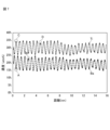
- FIG. 7 shows the positional variation of Ba concentration and Ti concentration in the ⁇ 100 ⁇ grain cross section. This is obtained by performing compositional analysis by energy dispersive X-ray spectroscopy (EDX) along a straight line on the ⁇ 100 ⁇ grain cross section and obtaining the atomic concentration obtained by this analysis as a function of position (distance).
- EDX energy dispersive X-ray spectroscopy
- Ba concentration and Ti concentration fluctuate periodically. Reflecting the positions of Ba and Ti in the crystal, the Ti concentration is the lowest at the position where the Ba concentration is maximum (peak), and the Ti concentration is highest at the position where the Ba concentration is minimum.
- the positional variation of the Ba concentration difference is sharp. That is, away from the origin, the Ba concentration rapidly decreases.
- the ⁇ 100 ⁇ grains of the prior art have a broad Ba concentration difference. This tendency reflects the bright spot size in the HAADF image. Therefore, in the graph of FIG. 8, the distance from the origin of the position where the Ba concentration difference ( ⁇ c) is 2 atm % is obtained, and the area of a circle whose radius is this distance is calculated. It can be regarded as the area (S ⁇ c ⁇ 2% ).
- a horizontal line is drawn along the horizontal axis when the Ba concentration difference ( ⁇ c) is 2 atm %. Then, the distances from the vertical axis to two points (a point and b point) where this line intersects the Ba concentration difference graph are read and defined as d a and d b , respectively. Then, the area of the atomic distribution region (S ⁇ c ⁇ 2% ) can be obtained according to the following formulas (2) and (3).
- the thickness of the dielectric ceramic layer is preferably 1.0 ⁇ m or less, particularly preferably 0.4 ⁇ m or less. By thinning the dielectric ceramic layer, it becomes possible to increase the capacity of the multilayer ceramic capacitor. However, if the dielectric ceramic layer is excessively thin, it becomes difficult to suppress deterioration in insulating properties.
- the thickness of the dielectric ceramic layer is typically 0.15 ⁇ m or more.
- the internal electrode layers contain a conductive metal.
- a conductive metal such as nickel (Ni), copper (Cu), silver (Ag), palladium (Pd), and alloys containing these may be used as the conductive metal.
- base metals such as Ni and Cu are preferable, and Ni is particularly preferable.
- the internal electrode layers may contain components other than the conductive metal.
- Other components may include ceramic components that act as co-materials. Examples of ceramic components include perovskite-type oxides such as BaTiO 3 -based compounds contained in the dielectric ceramic layer.
- the thickness of the internal electrode layer is preferably 0.20 ⁇ m or more and 0.80 ⁇ m or less. By setting the thickness of the internal electrode layer to 0.20 ⁇ m or more, defects such as electrode disconnection are suppressed. Further, by setting the thickness to 0.80 ⁇ m or less, it becomes possible to suppress the decrease in the ratio of the dielectric ceramic layer in the capacitor and the resulting decrease in capacitance.
- the number of internal electrode layers is preferably 15 or more and 700 or less.
- a known configuration can be adopted as the external electrode.
- it may be a laminated structure composed of an underlying layer, a first plated layer, and a second plated layer from the end face side of the laminated ceramic capacitor.
- the underlayer contains metal such as nickel (Ni) or copper (Cu).
- ceramic powder may be included in addition to the metal as a common material.
- the first plating layer is, for example, a nickel (Ni) plating layer.
- the second plating layer is, for example, a tin (Sn) plating layer.
- a conductive resin layer may be provided between the base layer and the first plating layer.
- the conductive resin layer is a layer containing conductive metal particles such as copper (Cu), silver (Ag) and nickel (Ni), and resin.
- the form of the external electrode is not limited as long as it is electrically connected to the internal electrode layer and functions as an external input/output terminal.
- a manufacturing method of the multilayer ceramic capacitor of the present embodiment is not limited as long as it satisfies the requirements described above. However, it is preferably manufactured by the following method.
- a preferred manufacturing method includes the following steps; a step of producing a green sheet containing at least a dielectric material (green sheet producing step); A step of obtaining a sheet (electrode pattern forming step), a step of laminating and crimping a plurality of green sheets to obtain a laminated block (lamination step), and a step of cutting the obtained laminated block to obtain a laminated chip (cutting step).
- a step of subjecting the obtained laminated chip to a binder removal treatment and a firing treatment to obtain an element body (firing step), and a step of forming external electrodes on the obtained element body (external electrode forming step).
- firing step a step of subjecting the obtained laminated chip to a binder removal treatment and a firing treatment to obtain an element body
- firing step a step of forming external electrodes on the obtained element body
- external electrode forming step provided.
- the laminated chip is fired while applying a pressure of 75 to 100 MPa in the thickness direction. Details of each step are described below.
- a green sheet is a precursor of a dielectric ceramic layer of a capacitor, and contains a main component raw material and an additive component raw material of the dielectric ceramic layer.
- the production of the green sheet may be performed by a known method, and is not particularly limited.
- a dielectric raw material is prepared by mixing additive component raw materials with a main component raw material, a binder and a solvent are added to and mixed with the obtained dielectric raw material to form a slurry, and a green sheet is formed from the obtained slurry.
- Powders of perovskite-type oxides such as BaTiO 3 -based compounds can be used as the raw material for the main component.
- the perovskite-type oxide powder may be synthesized by a known method such as a solid-phase reaction method, hydrothermal synthesis method, alkoxide method, or the like.
- known additives such as oxides, carbonates, hydroxides, nitrates, organic acid salts, alkoxides and/or chelate compounds of additive components (RE, Mn, Mg, Si, Al, and V) can be used as raw materials for additive components.
- a ceramic raw material may be used.
- Raw material mixing may be performed by a known method, for example, a method of wet-mixing and pulverizing the weighed main component raw material and additive component raw material together with grinding media and pure water using a ball mill. If wet mixing is used, the resulting mixture may be dried.
- Slurrying may also be performed by a known method, and the dielectric raw material may be mixed with an organic binder and an organic solvent.
- the organic binder a known binder such as a polyvinyl brural binder may be used.
- an organic solvent a known solvent such as toluene or ethanol may be used.
- Additives such as plasticizers may be added to the slurry as needed.
- the molding of the green sheet may also be performed by a known method such as a doctor blade method or a lip method.
- a conductive paste is applied to the surface of a green sheet to produce a green sheet having an internal electrode pattern formed thereon.
- the internal electrode patterns become internal electrode layers after firing.
- a conductive material such as nickel (Ni), copper (Cu), silver (Ag), palladium (Pd), or an alloy containing these may be used.
- a ceramic component that acts as a common material may also be added to the conductive paste.
- the ceramic component the raw material of the main component of the dielectric ceramic layer can be used.
- Application of the conductive paste may be performed by a known technique such as screen printing or gravure printing.
- ⁇ Lamination process> In the lamination step, a plurality of green sheets are laminated and pressure-bonded to produce a laminated block. In this case, green sheets with internal electrode patterns formed thereon are used, but some green sheets without internal electrode patterns may also be used. Lamination and crimping may be performed by a known method.
- the obtained laminated block is cut to produce laminated chips. Cutting may be performed so that chips of a predetermined size are obtained and at least a portion of the internal electrode pattern is exposed on the end face of the laminated chip.
- the laminated chip thus obtained is subjected to binder removal treatment and firing treatment to fabricate the element body.
- the firing process co-sinters the green sheets and the internal electrode patterns to form dielectric ceramic layers and internal electrode layers, respectively.
- the conditions for the binder removal treatment may be determined according to the types of organic binders contained in the green sheets and internal electrode patterns.
- the firing treatment may be performed at a temperature at which the laminated chip is sufficiently densified. For example, the temperature may be kept at 1200° C. or higher and 1300° C. or lower for 0 minute or longer and 30 minutes or shorter.
- the firing is carried out in an atmosphere in which the perovskite-type oxide, which is the main component, is not reduced and the oxidation of the conductive metal is suppressed.
- it may be carried out in an N 2 —H 2 —H 2 O airflow with an oxygen partial pressure of 10 ⁇ 10 to 10 ⁇ 12 MPa.
- annealing may be performed after firing.
- a dielectric material having a relatively high degree of crystallinity such as BaTiO 3 having a c-axis/a-axis ratio of 1.0085 or more, is used as the main component raw material.
- the laminated chip is held at a predetermined temperature for a predetermined time, and after the firing process, pressure is applied in the thickness direction by annealing. By performing annealing at a predetermined temperature while applying pressure in the stacking direction, stress is applied to crystal grains with a relatively high degree of crystallinity.
- the holding temperature is preferably 800° C. or more and 1000° C. or less, and the holding time (pressure application time) is preferably 30 minutes or more and 120 minutes or less.
- the applied pressure is preferably 1 MPa or more and 120 MPa or less. If the applied pressure is less than 1 MPa, the rearrangement of crystal grains becomes insufficient due to insufficient stress. Therefore, in the finally obtained multilayer ceramic capacitor, the proportion of ⁇ 100 ⁇ grains in the dielectric ceramic layers cannot be increased. On the other hand, if the pressure exceeds 120 MPa, the applied pressure becomes excessively high, which may cause defects such as cracking or chipping of the laminated chip.
- external electrodes are formed on the obtained element body. Formation of the external electrodes may be performed by a known method. For example, a conductive paste containing a metal such as silver (Ag), copper (Cu) and/or nickel (Ni) may be applied and baked on the exposed end surface of the element body where the internal electrodes are pulled out. . Alternatively, a technique may be used in which a conductive paste is applied to both end surfaces of the laminated chip before firing, and then firing treatment is performed. Further, the formed electrode may be used as a base layer, and a plating film such as nickel (Ni) or tin (Sn) may be formed thereon. A multilayer ceramic capacitor is manufactured through the formation of the external electrodes in this manner.
- a conductive paste containing a metal such as silver (Ag), copper (Cu) and/or nickel (Ni) may be applied and baked on the exposed end surface of the element body where the internal electrodes are pulled out. .
- a technique may be used in which a conductive paste is applied to
- Bam TiO 3 powder was prepared as a main component raw material.
- m is the A/B molar ratio of the perovskite oxide (ABO 3 ), that is, the Ba/Ti molar ratio.
- ABO 3 perovskite oxide
- Ba/Ti molar ratio As the BamTiO 3 powder, powder having a particle diameter D50 of 140 nm, a perovskite structure with a c-axis/a-axis ratio of 1.0090 and m of 1.005 was used.
- the prepared BamTiO 3 powder was weighed and wet-mixed by a ball mill to crush aggregates.
- raw materials for additive components (Dy, Mg, Mn, Si, Al, V) were weighed.
- Raw materials for additive components include dysprosium oxide ( Dy2O3 ), magnesium carbonate ( MgCO3 ), manganese carbonate ( MnCO3 ), silicon oxide ( SiO2 ), aluminum oxide ( Al2O3 ), and vanadium oxide (V2 ) . O 5 ) was used.
- Dy 1.0 mol part, Mg: 0.03 mol part, Mn: 0.1 mol part, Si: 0.8 mol part, Al: 0.08 mol part and V: 0.08 mol part.
- the additive component raw materials were added to the main component raw materials, wet-mixed using a ball mill, dried and heat-treated to obtain dielectric raw materials.
- a polyvinyl butyral-based binder and ethanol as an organic solvent were added to the obtained dielectric raw material, and wet-mixed by a ball mill for a predetermined time to prepare a slurry. This slurry was formed into a sheet to produce a green sheet for a dielectric ceramic layer.
- a conductive paste mainly composed of Ni was screen-printed on the surface of the obtained green sheet to form a pattern of conductive paste layers that would become internal electrode layers.
- a plurality of green sheets each having a conductive paste layer formed thereon were laminated, and green sheets without a conductive paste layer formed thereon were placed above and below the green sheets, and the whole was pressed together to produce a laminated block.
- the obtained laminated block was cut with a dicing saw into laminated chips. Lamination was performed so that the ends from which the conductive paste layers were drawn out were alternated. Also, the cutting was performed so that the conductive paste layer was exposed on the side surface.
- a side margin green sheet (side margin green body) was pasted on both sides of the cut laminated chip where the conductive paste layer was exposed. Side margin green sheets were produced in the same manner as the dielectric ceramic layer green sheets.
- the laminated chip with the side margin green body attached was placed in an N 2 —H 2 O—H 2 stream at an oxygen partial pressure of 1.8 ⁇ 10 ⁇ 9 to 8.7 ⁇ 10 ⁇ 10 MPa at a temperature elevation rate of 20° C. / sec, maximum temperature 1260°C x 0.5 hours. After sintering, it was annealed in an atmosphere of oxygen partial pressure of 1.0 ⁇ 10 ⁇ 12 to 10 ⁇ 15 MPa and 800 to 1000° C. while applying pressure in the stacking direction to obtain a multilayer ceramic capacitor body.
- a conductive paste containing copper (Cu) as a main component was applied to the end faces of the element obtained by firing where the internal electrode layers were drawn out. After that, the applied conductive paste was baked at 900° C. to form a base layer for the external electrodes. Further, Ni plating and Sn plating were performed in this order on the surface layer of the underlayer by wet plating. Thus, a laminated ceramic capacitor was produced.
- Cu copper
- the manufactured multilayer ceramic capacitor had a length L dimension of 0.4 mm, a width direction W dimension of 0.2 mm, and a thickness direction T dimension of 0.2 mm.
- the dielectric layers had a thickness of 0.5 ⁇ m
- the internal electrode layers had a thickness of 0.4 ⁇ m
- the number of dielectric ceramic layers was 150.
- ⁇ Dielectric properties> The capacitance C of the multilayer ceramic capacitor was measured using an automatic bridge type measuring machine. The measurement was performed under the conditions of a temperature of 25° C., an effective voltage of 0.5 Vrms, and a frequency of 1 kHz. Then, using the capacitance C, the dielectric constant ( ⁇ r ) of the dielectric ceramic layer was obtained. Also, the relative permittivity value of Comparative Example 1 was used as a reference, and the relative permittivity ratio ( ⁇ r ratio) was obtained.
- S-TEM scanning transmission electron microscope
- a thin film was processed by a focused ion beam (FIB) method to prepare an observation sample.
- FIB focused ion beam
- a thin sample having a thickness of 100 nm or less and having a plane (WT plane) including the width direction and the thickness direction was taken out from the central portion of the laminated ceramic capacitor in the length direction (L direction).
- This flake sample had a thickness smaller than the radius of the grains contained in the sample.
- the EDX device attached to the S-TEM was used to obtain the Ba concentration and Ti concentration in the cross section of the ⁇ 100 ⁇ grain as a function of distance (positional variation) and graphed.
- An example of the obtained graph is shown in FIG.
- point A is a point where the positional variation of Ba concentration is relatively sharp
- point B is a point where it is relatively broad
- point C is a point where the positional variation of the Ti concentration is relatively sharp
- point D is a point where it is relatively broad. It is conceivable that the locations with sharp positional fluctuations have small lattice distortions, while the locations with broad positional fluctuations have large lattice distortions.
- FIGS. 8 and 9 show the results obtained for BaTiO 3 produced by the conventional technique.
- each area (S ⁇ c ⁇ 2% ) of the Ba atom distribution region and the Ti atom distribution region was obtained. Specifically, a line was drawn horizontally on the horizontal axis where the Ba concentration difference ( ⁇ c) is 2 atm %. Then, the distances from the vertical axis to two points (a point and b point) where this line intersects the Ba concentration difference graph were read and defined as d a and d b , respectively. Then, the area of the atomic distribution region (S ⁇ c ⁇ 2% ) was calculated according to the following formulas (2) and (3). The area of the atomic distribution region was calculated for all the detected ⁇ 100 ⁇ particles, and the average value of 10 particles selected in ascending order of area was obtained.
- Table 1 below summarizes the pressure conditions during firing and the characteristics of the dielectric ceramic layers for Comparative Example 1 and Examples 1 to 20.
- Table 1 below shows the area of the Ba atom distribution region (S ⁇ c ⁇ 2% ).
- the area of the Ti atom distribution region was almost the same as the value for Ba.
- Examples 5, 6, 8 and 11 to 20 with a number ratio of 3% or more had a dielectric constant of 3220 or more
- Examples 15 to 20 with a number ratio of 6% or more had a dielectric constant of 3530 or more.
- the higher the applied pressure and the longer the applied time the smaller the area of the atomic distribution region (S ⁇ c ⁇ 2% ), and the higher the high temperature load life (MTTF).
- the MTTF is 36 hours or more
- the MTTF is 70 hours or more. there were.
Abstract
誘電体セラミック層の誘電率を高めることができ、小型化及び大容量化が可能な積層セラミックコンデンサが提供される。この積層セラミックコンデンサは、厚さ方向に相対する第1主面及び第2主面、幅方向に相対する第1側面及び第2側面、並びに長さ方向に相対する第1端面及び第2端面を有し、前記厚さ方向に積層された複数の誘電体セラミック層及び複数の内部電極層を含む素体部と、前記第1端面及び第2端面のそれぞれに設けられ、前記複数の内部電極層と接続された一対の外部電極と、を備える。前記誘電体セラミック層は、Aサイト元素及びBサイト元素を含むペロブスカイト型酸化物で構成された結晶粒子を含む。走査透過電子顕微鏡(S-TEM)を用いて前記誘電体セラミック層の断面を観察したときに、ペロブスカイト型構造の{100}面が観測される{100}粒子を結晶粒子として前記誘電体セラミック層が含む。前記誘電体セラミック層の厚さをdとしたときに、前記誘電体セラミック層の内部であって且つ隣接する内部電極層との界面からの距離が0.1d以下の電極近傍領域に、前記{100}粒子の少なくとも一部が存在する。
Description
本発明は、積層セラミックコンデンサに関する。
携帯電話を始めとする電子機器の小型化やCPUの高速化に伴い、積層セラミックコンデンサ(MLCC)への需要がますます高くなっている。積層セラミックコンデンサは、誘電体セラミック層と内部電極層とが交互に積層された構造を有しており、薄層化された高誘電率誘電体セラミック層に起因して、小型でありながら大きな静電容量をもつ。種々の材料を備えた積層セラミックコンデンサが知られているが、誘電体セラミック層にチタン酸バリウム(BaTiO3)系化合物を用い、内部電極層にニッケル(Ni)などの卑金属を用いたものが、安価で且つ高特性を示すため、広く利用されている。
積層セラミックコンデンサの小型化及び大容量化を実現する上で、誘電体セラミック層を薄層化すると同時に、その誘電率を高めることが重要である。すなわち内部電極層の対向面積をS、内部電極層間に挟まれる誘電体セラミック層の層数をn、誘電体セラミック層の比誘電率をεr、誘電体セラミック層の厚さをt、真空の比誘電率をε0とすると、積層セラミックコンデンサの静電容量Cは、下記(1)式に示されるように比誘電率εrに比例する。

この点、誘電体セラミック層の組成やその分布、または結晶粒子の粒径などを制御することで誘電率を高めることが従来から提案されている。例えば、特許文献1には、チタン酸バリウムを主成分とする結晶粒子によって構成された誘電体磁器と、この誘電体磁器を誘電体層に適用した積層セラミックコンデンサに関して、希土類元素濃度を結晶粒子表面で最大とし、表面から100nmよりも深い領域で0.1原子%以下にすることが開示されている(特許文献1の請求項1及び[0001])。また結晶粒子は、内部の領域(コア部)で希土類元素をほとんど含まないことから、この領域に強誘電性を示す結晶相が多く割合で含まれており、これにより強誘電率化が可能になると記載されている(特許文献1の[0016]及び[0018])。
特許文献2には、セラミック誘電体層がコアシェル粒子と均一固溶粒子とを含む焼結体粒子からなり、焼結体粒子全体に対して占めるコアシェル粒子の面積比率が5~15%であり、焼結体粒子全体の平均粒径が0.3~0.5μmである積層セラミックコンデンサが開示されている(特許文献2の請求項1)、またセラミック誘電体層の厚さを2.0μm以下に薄層化する場合であっても、誘電体層の比誘電率を5000以上とし、同時に安定した静電容量温度特性を有する積層セラミックコンデンサを提供できると記載されている(特許文献2の請求項1及び[0016])。
特許文献3には、誘電体層がチタン酸バリウム及びケイ素化合物を含む焼結体からなり、誘電体層には、平均結晶粒子径が1μm以下のフレストナイト相が存在している積層セラミックコンデンサが開示されている(特許文献3の請求項1)。またフレストナイト相が形成されると、添加化合物のチタン酸バリウムへの固溶が促進され、焼成による粒成長が促進されて、一粒子当たりの誘電率が上昇すると記載されている(特許文献3の[0047])。
このように、積層セラミックコンデンサにおいて、誘電体セラミック層の組成やその分布、結晶粒径などを制御して誘電率を高めることが提案されている。しかしながら、このような従来の手法は、一定の効果があるものの、積層セラミックコンデンサの小型化及び大容量を図る上で限界がある。
本発明者らは、このような問題点に鑑みて鋭意検討を行った。その結果、ペロブスカイト型酸化物を主成分として含む誘電体セラミック層と内部電極層とを備える積層セラミックコンデンサにおいて、誘電体セラミック層を構成する結晶粒子の結晶面に着目し、これを制御することで、誘電体セラミック層の誘電率を高めることができ、その結果、積層セラミックコンデンサのより一層の小型化及び大容量化が可能になるとの知見を得た。
本発明は、このような知見に基づき完成されたものであり、誘電体セラミック層の誘電率を高めることができ、小型化及び大容量化が可能な積層セラミックコンデンサの提供を課題とする。
本発明は、以下の態様を包含する。なお本明細書において「~」なる表現は、その両端の数値を含む。すなわち「X~Y」は「X以上Y以下」と同義である。
本発明の一態様によれば、厚さ方向に相対する第1主面及び第2主面、幅方向に相対する第1側面及び第2側面、並びに長さ方向に相対する第1端面及び第2端面を有し、
前記厚さ方向に積層された複数の誘電体セラミック層及び複数の内部電極層を含む素体部と、前記第1端面及び第2端面のそれぞれに設けられ、前記複数の内部電極層と接続された一対の外部電極と、を備える積層セラミックコンデンサであって、
前記誘電体セラミック層は、Aサイト元素及びBサイト元素を含むペロブスカイト型酸化物で構成された結晶粒子を含み、
走査透過電子顕微鏡(S-TEM)を用いて前記誘電体セラミック層の断面を観察したときに、ペロブスカイト型構造の{100}面が観測される{100}粒子を結晶粒子として前記誘電体セラミック層が含み、
前記誘電体セラミック層の厚さをdとしたときに、前記誘電体セラミック層の内部であって且つ隣接する内部電極層との界面からの距離が0.1d以下の電極近傍領域に、前記{100}粒子の少なくとも一部が存在する、積層セラミックコンデンサが提供される。
本発明によれば、誘電体セラミック層の誘電率を高めることができ、小型化及び大容量化が可能な積層セラミックコンデンサが提供される。
本発明の具体的な実施形態(以下、「本実施形態」という)について説明する。なお本発明は以下の実施形態に限定されるものではなく、本発明の要旨を変更しない範囲において種々の変更が可能である。
(1)積層セラミックコンデンサ
本実施形態の積層セラミックコンデンサは、厚さ方向に相対する第1主面及び第2主面、幅方向に相対する第1側面及び第2側面、並びに長さ方向に相対する第1端面及び第2端面を有し、厚さ方向に積層された複数の誘電体セラミック層及び複数の内部電極層を含む素体部と、第1端面及び第2端面のそれぞれに設けられ、複数の内部電極層と接続された一対の外部電極と、を備える。この積層セラミックコンデンサにおいて、誘電体セラミック層は、Aサイト元素及びBサイト元素を含むペロブスカイト型酸化物で構成された結晶粒子を含む。また走査透過電子顕微鏡(S-TEM)を用いて誘電体セラミック層の断面を観察したときに、ペロブスカイト型構造の{100}面が観測される{100}粒子を結晶粒子として誘電体セラミック層が含む。さらに誘電体セラミック層の厚さをdとしたときに、誘電体セラミック層の内部であって且つ隣接する内部電極層との界面からの距離が0.1d以下の電極近傍領域に、{100}粒子の少なくとも一部が存在する。
本実施形態の積層セラミックコンデンサは、厚さ方向に相対する第1主面及び第2主面、幅方向に相対する第1側面及び第2側面、並びに長さ方向に相対する第1端面及び第2端面を有し、厚さ方向に積層された複数の誘電体セラミック層及び複数の内部電極層を含む素体部と、第1端面及び第2端面のそれぞれに設けられ、複数の内部電極層と接続された一対の外部電極と、を備える。この積層セラミックコンデンサにおいて、誘電体セラミック層は、Aサイト元素及びBサイト元素を含むペロブスカイト型酸化物で構成された結晶粒子を含む。また走査透過電子顕微鏡(S-TEM)を用いて誘電体セラミック層の断面を観察したときに、ペロブスカイト型構造の{100}面が観測される{100}粒子を結晶粒子として誘電体セラミック層が含む。さらに誘電体セラミック層の厚さをdとしたときに、誘電体セラミック層の内部であって且つ隣接する内部電極層との界面からの距離が0.1d以下の電極近傍領域に、{100}粒子の少なくとも一部が存在する。
積層セラミックコンデンサの一態様を、図1~図3を用いて説明する。図1は積層セラミックコンデンサの外形を示す斜視図である。図2及び図3は積層セラミックコンデンサの内部構造を示す断面図である。積層セラミックコンデンサ(100)は、積層された複数の誘電体セラミック層(2)及び複数の内部電極層(4)を含む素体部(6)と、この素体部(6)の両端面(14a、14b)に設けられた一対の外部電極(8a、8b)と、を備える。積層セラミックコンデンサ(100)及び素体部(6)は、略直方体の形状を有する。略直方体とは、直方体のみならず、角部及び/又は稜部が丸められた直方体を包含する。また積層セラミックコンデンサ(100)及び素体部(6)は、厚さ方向Tに相対する第1主面(10a)及び第2主面(10b)、幅方向Wに相対する第1側面(12a)及び第2側面(12b)、並びに長さ方向Lに相対する第1端面(14a)及び第2端面(14b)を有する。ここで厚さ方向Tとは、複数の誘電体セラミック層(2)及び複数の内部電極層(4)が積層された方向を指す。長さ方向Lは、外部電極(8a、8b)が設けられた端面(14a、14b)に直交する方向を指す。幅方向Wは厚さ方向T及び長さ方向Lに直交する方向である。厚さ方向T及び幅方向Wを含む面をWT面と定義し、幅方向W及び長さ方向Lを含む面をLW面と定義し、長さ方向L及び厚さ方向Tを含む面をLT面と定義する。
外部電極(8a、8b)は、第1端面(14a)に設けられた第1外部電極(8a)と、第2端面(14b)に設けられた第2外部電極(8b)と、から構成される。第1外部電極(8a)は、第1端面(14a)のみならず、第1主面(10a)、第2主面(10b)、第1側面(12a)及び第2側面(12b)の一部に回り込んでもよい。また第2外部電極(8b)は、第2端面(14b)のみならず、第1主面(10a)、第2主面(10b)、第1側面(12a)及び第2側面(12b)の一部に回り込んでもよい。しかしながら、第1外部電極(8a)と第2外部電極(8b)は接触しておらず、電気的に離間している。
内部電極層(4)は、複数の第1内部電極層(4a)と複数の第2内部電極層(4b)とから構成される。第1内部電極層(4a)は第1端面(14a)に延在し、そこで第1外部電極(8a)と電気的に接続されている。また第2内部電極層(4b)は第2端面(14b)に延在し、そこで第2外部電極(8b)と電気的に接続されている。誘電体セラミック層(2)を挟んで対向する第1内部電極層(4a)と第2内部電極層(4b)は、電気的に接続されていない。そのため外部電極(8a、8b)を介して第1内部電極層(4a)と第2内部電極層(4b)との間に電圧が印加されると、電荷が蓄積される。蓄積された電荷により静電容量が生じ、それにより容量素子としての機能が発現する。
積層セラミックコンデンサ(100)の寸法は、特に限定されない。しかしながら、長さ方向L寸法は0.2mm以上1.2mm以下、幅方向W寸法は0.1mm以上0.7mm以下、積層方向T寸法は0.1mm以上0.7mm以下が好ましい。
<誘電体セラミック層>
誘電体セラミック層は結晶粒子を含む。この結晶粒子は、誘電体セラミック層の主成分となる粒子(主結晶粒子)であり、Aサイト元素及びBサイト元素を含むペロブスカイト型酸化物で構成される。すなわち、誘電体セラミック層は、ペロブスカイト型酸化物を主成分とする焼結多結晶体である。ペロブスカイト型酸化物は、一般式:ABO3で表される組成を有しており、室温で立方晶、正方晶、斜方晶、及び菱面体晶などの立方晶類似の結晶構造をもつ。またAサイト元素の原子(以下、「Aサイト原子」)及びBサイト元素の原子(以下、「Bサイト原子」)のそれぞれは、イオン化してペロブスカイト構造のAサイト及びBサイトを占める。Aサイト元素として、バリウム(Ba)、カルシウム(Ca)、及びストロンチウム(Sr)などのイオンサイズが比較的大きい元素が例示され、またBサイト元素として、チタン(Ti)、ジルコニウム(Zr)、及びハフニウム(Hf)などのイオンサイズが比較的小さい元素が例示される。
誘電体セラミック層は結晶粒子を含む。この結晶粒子は、誘電体セラミック層の主成分となる粒子(主結晶粒子)であり、Aサイト元素及びBサイト元素を含むペロブスカイト型酸化物で構成される。すなわち、誘電体セラミック層は、ペロブスカイト型酸化物を主成分とする焼結多結晶体である。ペロブスカイト型酸化物は、一般式:ABO3で表される組成を有しており、室温で立方晶、正方晶、斜方晶、及び菱面体晶などの立方晶類似の結晶構造をもつ。またAサイト元素の原子(以下、「Aサイト原子」)及びBサイト元素の原子(以下、「Bサイト原子」)のそれぞれは、イオン化してペロブスカイト構造のAサイト及びBサイトを占める。Aサイト元素として、バリウム(Ba)、カルシウム(Ca)、及びストロンチウム(Sr)などのイオンサイズが比較的大きい元素が例示され、またBサイト元素として、チタン(Ti)、ジルコニウム(Zr)、及びハフニウム(Hf)などのイオンサイズが比較的小さい元素が例示される。
ペロブスカイト型酸化物の結晶構造を図4に示す。Ti4+などのイオン化したBサイト原子(以下、「Bサイトイオン」)が単位胞の体心の位置を占め、面心の位置にあり正八面体を形成する6個の酸素イオン(O2-)によって囲まれている。またBa2+などのイオン化したAサイト原子(以下、「Aサイトイオン」)が単位胞の8個の隅部を占める。正電荷をもつAサイトイオン及び/又はBサイトイオンが変位することで誘電分極が生じ、それにより室温で常誘電又は強誘電的な性質を示す。なお、本明細書では、イオン化した原子(イオン)を単に「原子」と呼ぶ場合がある。
Aサイト元素及びBサイト元素の組み合わせは、ペロブスカイト型構造を維持する限り、特に限定はされない。またAサイト元素及びBサイト元素のそれぞれは、一種類の元素のみを含んでもよく、あるいは複数の元素を組み合わせて含んでもよい。さらに誘電体セラミック層中のペロブスカイト型酸化物の含有割合は、50質量%以上であってよく、60質量%以上であってよく、70質量%以上であってよく、80質量%以上であってよく、90質量%以上であってもよい。
好ましくは、Aサイト元素はバリウム(Ba)を含み、且つBサイト元素はチタン(Ti)を含む。すなわちペロブスカイト型酸化物はチタン酸バリウム(BaTiO3)系化合物であってよい。BaTiO3は室温で大きな自発分極をもつ。そのため高い誘電率を示す強誘電体である。したがってBaTiO3系化合物を主成分にすることで、コンデンサのより一層の大容量化を図ることが可能になる。なおBaTiO3系化合物は、BaTiO3のみならず、BaTiO3のBaの一部をSr及び/又はCaなどの他のAサイト元素で置換したもの、あるいはTiの一部をZr及び/又はHfなどの他のBサイト元素で置換したものを包含する。ただし、Aサイト元素中のBaの割合は、モル比で70%以上が好ましく、80%以上がより好ましく、90%以上がさらに好ましい。またBサイト元素中のTiの割合は、モル比で70%以上が好ましく、80%以上がより好ましく、90%以上がさらに好ましい。Aサイト元素がBa及び不可避不純物元素以外の成分を含まず、またBサイト元素がTi及び不可避不純物元素以外の成分を含まなくてもよい。ここで、不可避不純物とは、製造工程時に不可避的に混入する成分である。
誘電体セラミック層は、主成分以外の他の成分を添加成分として含んでもよい。添加成分として、限定される訳ではないが、希土類元素(RE)、マンガン(Mn)、マグネシウム(Mg)、ケイ素(Si)、アルミニウム(Al)、及びバナジウム(V)などが挙げられる。希土類元素(RE)は、周期律表において原子番号21のスカンジウム(Sc)、原子番号39のイットリウム(Y)、及び原子番号57のランタン(La)~原子番号71のルテチウム(Lu)からなる群を構成する元素の総称である。希土類元素(RE)として、イットリウム(Y)、プラセオジウム(Pr)、ネオジム(Nd)、サマリウム(Sm)、ユウロピウム(Eu)、ガドリニウム(Gd)、テルビウム(Tb)、ジスプロシウム(Dy)、ホルミウム(Ho)、エルビウム(Er)、ツリウム(Tm)、イッテルビウム(Yb)、及びルテチウム(Lu)からなる群から選択される一種以上が好ましく、ジスプロシウム(Dy)が特に好ましい。また添加成分の存在形態は限定されない。結晶粒子、粒界、及び三重点のいずれかに含まれていればよい。結晶粒子に含まれる場合には、ペロブスカイト型酸化物(ABO3)のAサイトを占めてもよく、Bサイトを占めてもよく、あるいは両方のサイトを同時に占めてもよい。
本実施形態の積層セラミックコンデンサにおいて、誘電体セラミック層は結晶粒子として{100}粒子を含む。ここで{100}粒子とは、走査透過電子顕微鏡(Scanning Transmission Electron Microscopy;S-TEM)を用いて誘電体セラミック層の断面を観察したときに、その少なくとも一部において、ペロブスカイト型構造の{100}面が観測される結晶粒子のことである。すなわち結晶粒子の一部又は全部が{100}粒子である。また{100}粒子において、その少なくとも一部の領域で{100}面が観測されればよい。断面とは、厚さ方向、すなわち誘電体セラミック層と内部電極層の積層方向を含む面である。断面は、その垂線が厚さ方向と直交する面ということもでき、例えばLT面やWT面である。さらに{100}面は、ミラー指数で表される結晶格子面であり、(100)面、(010)面、(001)面、(-100)面、(0-10)面、(00-1)面の6面を包含する。
走査透過電子顕微鏡(S-TEM)は、収束した微小入射プローブを試料上で走査し、透過電子を輝度信号に変換して微細構造を観察する装置である。近年の装置の進歩により、空間分解能は50pm以下にまで向上しており、検出感度においても単原子レベルまで捉えられるようになっている。S-TEMでは、試料から散乱された電子を用いて様々な像の観察が可能である。このような像のうち、円環状の検出器を用いて入射プローブの収束角よりも大きな散乱角の電子を検出して得た像が、環状暗視野(Annular Dark-Field;ADF)像である。またADF像のうち散乱角度の特に大きい像が、高角環状暗視野(High Angle Annular Dark-Field;HAADF)像である。HAADFの強度は原子番号Zに応じているため、HAADF像は元素識別能に優れている。したがって、特にHAADF像を解析することで、元素の位置情報を高精度に評価することができる。
{100}粒子の有無及びその割合は、誘電体セラミック層を構成する結晶粒子の中央部についてADF像、HAADF像及び/又は電子線回折図形を求め、これらを解析して調べることができる。具体的には、S-TEM観察の際にナノビーム電子回折(Nano Beam electron Diffraction;NBD)法で、特定の粒子中央部のADF像又はHAADF像を得る。そして、この像において、ペロブスカイト型酸化物を構成する原子の配列に基づく{100}面が観察される場合に、その粒子を{100}粒子と判断することができる。あるいはNBD法で電子線回折図形を求め、この電子線回折図形に{100}面に基づく周期パターンのみが存在する場合に、その粒子を{100}粒子と判断してもよい。
S-TEM観察は、誘電体セラミック層の厚さ方向を含む断面について行う。より具体的には、誘電体セラミック層の長さ方向(L方向)中央部に位置するとともに、幅方向(W方向)及び厚さ方向(T方向)を含む面(WT面)の中央部における領域について、観察することが好ましい。観察は、視野10μm×10μmの領域または結晶粒を200個含む領域について行えばよい。またS-TEM観察は、誘電体セラミック層断面に略垂直な方向に顕微鏡軸を固定し、その状態で誘電体セラミック層断面を±5°の範囲内で傾斜させて行う。そして傾斜角がこの範囲(±5°)内で{100}面が観測される粒子を{100}粒子と定める。要するに、誘電体セラミック層断面の垂直軸に対して±5°の範囲内に{100}面が露出している粒子が{100}粒子である。
{100}粒子について、実際の測定結果に基づき、さらに詳細に説明する。本実施形態の積層セラミックコンデンサの誘電体セラミック層中に含まれる{100}粒子の断面HAADF像の一例を図5に示す。この積層セラミックコンデンサは、チタン酸バリウム(BaTiO3)を誘電体セラミック層に用いている。図5において、Baに基づく輝点とTiに基づく輝点が観察され、これらの輝点はそれぞれ格子状の原子(イオン)配列を構成している。またBa輝点は、その輝度がTi輝点より高い。これはBaの原子量がTiよりも大きいからである。
本実施形態の積層セラミックコンデンサにおいて、誘電体セラミック層の厚さをdとしたときに、電極近傍領域に{100}粒子の少なくとも一部が存在する。ここで電極近傍領域とは、誘電体セラミック層の内部であって且つ隣接する内部電極層との界面からの距離が、厚さdの10%、すなわち0.1d以下の領域のことである。誘電体セラミック層は、その上面及び下面の2面で内部電極層と接している。したがって、誘電体セラミック層は、その上部及び下部のそれぞれに厚さ0.1dの電極近傍領域を備えている。電極近傍領域に{100}粒子を設けることで、誘電体セラミック層の誘電率を高めることが可能になる。そのメカニズムの詳細は不明であるが、Ni電極近傍領域では、Niの圧縮応力が大きくなるため、誘電体セラミックスがNi電極との垂直方向にC軸配向しやすく、より比誘電率が高くなるのではないかと推測している。なお、{100}粒子は、その少なくとも一部が電極近傍領域に含まれていればよい。すなわち、{100}粒子の一部が電極近傍領域に含まれ、他の部分が電極近傍領域に含まれていなくても、この粒子は電極近傍領域に存在すると判断してよい。
誘電体セラミック層に含まれる{100}粒子は、その少なくとも一部が電極近傍領域に存在すればよい。換言するに、電極近傍領域に含まれる結晶粒子のうち、少なくとも一部が{100}粒子であればよい。{100}粒子の一部が電極近傍領域に存在してもよく、あるいは全部が電極近傍領域に存在してもよい。しかしながら、{100}粒子のうち、電極近傍領域に存在する粒子の割合は高いほど好ましい。具体的には、上述した断面において、誘電体セラミック層に含まれる{100}粒子のうち、電極近傍領域に存在する{100}粒子の個数割合は1%以上がより好ましく、3%以上がさらに好ましい。
好ましくは、上述した断面、すなわち誘電体セラミック層の厚さ方向を含む断面において、{100}粒子のうち、その少なくとも一部は内部電極層に接して存在する。すなわち、内部電極層に接する結晶粒子のうち、少なくとも一部が{100}粒子であることが好ましい。{100}粒子を内部電極層に接して設けることで、誘電体セラミック層の誘電率をより一層高めることが可能になる。内部電極層に接する{100}粒子の割合は高いほど好ましい。上述した断面において、誘電体セラミック層に含まれる{100}粒子のうち、内部電極層に接する{100}粒子の個数割合は、1%以上が好ましく、2%以上がより好ましく、3%以上がさらに好ましく、4%以上がよりさらに好ましく、5%以上が特に好ましく、6%以上が最も好ましい。
好ましくは、上述した断面において{100}粒子は、粒子内の1つ以上の原子位置において原子分布領域をもち、この原子分布領域の面積(SΔc≦2%)が0.070nm2以下である。ここで原子分布領域とは、格子点を中心とする原子の位置分布の拡がりの目安となるものである。具体的には、ADF像又はHAADF像において一つの格子点を中心とする単位胞の内部に存在し、この格子点に対応するAサイト元素又はBサイト元素の原子濃度差分(Δc)が2atm%以下となる単領域である。ここで、原子濃度差分(Δc)とは、この単位胞の内部において、この元素(Aサイト元素又はBサイト元素)の原子濃度(c)の、その最大値(cmax)からの差分(cmax-c)である。
理想的な結晶では、絶対零度で原子又はイオンは、それが占めるべき格子点のみに存在する。しかしながら、絶対零度超の温度ではフォノンが生じて、原子又はイオンは格子点の周囲を熱振動(格子振動)する。また、現実の結晶では、格子欠陥などの欠陥が生じ、それにより格子点からずれた位置に原子が配置されることがある。これは欠陥により結晶場が変化するためである。そのため、原子の位置分布に拡がりが生じる。すなわち、ある一つの格子点を中心とする単位胞に着目すると、この格子点を占めるべき原子の濃度は、格子点で最大となり、格子点から離れるに従い小さくなる。したがって、原子分布領域の大きさを定量的に見積もることができれば、それにより原子位置分布の拡がりを評価できる。
原子分布領域の面積(SΔc≦2%)を小さくすることで、積層セラミックコンデンサの高温負荷寿命が長くなり、その結果、信頼性を高めることが可能になる。そのメカニズムの詳細は不明であるが、次のように推測している。すなわち現実の結晶には、酸素空孔や原子欠陥などの格子欠陥が多数存在する。特に積層セラミックコンデンサは、還元性雰囲気下で焼成して製造されることから、これに含まれる誘電体セラミック層には、多数の酸素空孔が存在すると考えられる。そして、この酸素空孔が積層セラミックコンデンサの高温負荷寿命を短くする要因と考えられている。また酸素空孔等の格子欠陥が多数存在すると、格子の歪みをもたらすことで元素の位置分布が拡がり、その結果、原子分布領域の面積が大きくなると考えられる。これに対して、原子分布領域の面積が小さいと、格子欠陥が少なくなり、高温負荷寿命が長くなる。原子分布領域の面積は小さいほど好ましい。面積は0.070nm2以下が好ましく、0.060nm2以下がより好ましく、0.050nm2以下がさらに好ましく、0.040nm2以下がよりさらに好ましく、0.030nm2以下が特に好ましく、0.020nm2以下が最も好ましい。下限値は特に限定されない。例えば、面積は0.001nm2以上である。
原子分布領域の(SΔc≦2%)の面積について、実際の測定結果に基づき、さらに詳細に説明する。本実施形態の積層セラミックコンデンサの誘電体セラミック層中に含まれる{100}粒子の断面HAADF像の一例を図5に示す。また従来技術で得られた積層セラミックコンデンサの断面HAADF像を図6に示す。ここで、本実施形態及び従来技術の積層セラミックコンデンサは、いずれもチタン酸バリウム(BaTiO3)を誘電体セラミック層に用いている。図5及び図6のいずれにおいても、Baに基づく輝点とTiに基づく輝点が観察され、これらの輝点はそれぞれ格子状の原子(イオン)配列を構成している。しかしながら、本実施形態の{100}粒子では輝点サイズが小さいのに対し、従来技術の{100}粒子では輝点サイズが大きい。これは、本実施形態の{100}粒子では、イオン化したBa及びTiの原子分布領域が格子点近傍に集中しているのに対し、従来技術の{100}粒子ではBa及びTiの格子に歪みが生じ、原子分布領域が拡がっているからである。
次に、原子分布領域の面積(SΔc≦2%)の測定方法について説明する。図7は、{100}粒子断面におけるBa濃度とTi濃度の位置変動を示す。これは、{100}粒子断面の一直線上に沿ってエネルギー分散型X線分光(EDX)法で組成分析を行い、この分析によって得られた原子濃度を位置(距離)の関数として求めたものである。Ba濃度及びTi濃度は周期的に変動する。また結晶中でのBaとTiの位置を反映して、Ba濃度が最大(ピーク)になる位置でTi濃度は最小になり、Ba濃度が最小になる位置でTi濃度は最大になる。
図8は、図7においてBa濃度(c)が最大(cmax)となる位置を原点とし、そこから30pm間隔でBa濃度の差分(Δc=cmax-c)を一格子分についてグラフ化したものである。本実施形態の{100}粒子ではBa濃度差分の位置変動がシャープである。すなわち原点を離れると、Ba濃度が急速に小さくなる。これに対して、従来技術の{100}粒子ではBa濃度差分がブロードである。この傾向はHAADF像での輝点サイズを反映している。したがって、図8のグラフにおいて、Ba濃度の差分(Δc)が2atm%となる位置の原点からの距離を求め、この距離を半径とする円の面積を算出すれば、これをBa原子分布領域の面積(SΔc≦2%)と見なすことができる。
具体的には、図8のグラフにおいて、Ba濃度の差分(Δc)が2atm%となるラインを横軸に水平に描く。そしてこのラインがBa濃度差分のグラフと交差する2点(a点及びb点)の縦軸からの距離を読み取り、それぞれda及びdbとする。そして、下記(2)及び(3)式にしたがって、原子分布領域の面積(SΔc≦2%)を求めることができる。

誘電体セラミック層は、その厚さが、好適には1.0μm以下、特に好適には0.4μm以下である。誘電体セラミック層を薄層化することで、積層セラミックコンデンサの大容量化を図ることが可能になる。しかしながら誘電体セラミック層が過度に薄層化されると、絶縁特性の低下を抑えることが困難になる。誘電体セラミック層の厚さは、典型的には0.15μm以上である。
<内部電極層>
内部電極層は導電性金属を含む。導電性金属として、ニッケル(Ni)、銅(Cu)、銀(Ag)、パラジウム(Pd)、及びこれらを含む合金などの公知の電極材料を用いればよい。しかしながら、低コスト化の観点から、卑金属たるNiやCuが好適であり、Niが特に好適である。内部電極層は、導電性金属以外の他の成分を含んでもよい。他の成分として、共材として働くセラミック成分を挙げることができる。セラミック成分として、誘電体セラミック層に含まれるBaTiO3系化合物などのペロブスカイト型酸化物が例示される。
内部電極層は導電性金属を含む。導電性金属として、ニッケル(Ni)、銅(Cu)、銀(Ag)、パラジウム(Pd)、及びこれらを含む合金などの公知の電極材料を用いればよい。しかしながら、低コスト化の観点から、卑金属たるNiやCuが好適であり、Niが特に好適である。内部電極層は、導電性金属以外の他の成分を含んでもよい。他の成分として、共材として働くセラミック成分を挙げることができる。セラミック成分として、誘電体セラミック層に含まれるBaTiO3系化合物などのペロブスカイト型酸化物が例示される。
内部電極層の厚さは、好適には0.20μm以上0.80μm以下である。内部電極層の厚さを0.20μm以上にすることで、電極途切れなどの不良が抑制される。また厚さを0.80μm以下にすることで、コンデンサ中の誘電体セラミック層が占める割合の低下、及びそれによる容量低下を抑制することが可能になる。また内部電極層の層数は、好適には15枚以上700枚以下である。
<外部電極>
外部電極として、公知の構成を採用できる。例えば、積層セラミックコンデンサの端面側から、下地層、第1めっき層、及び第2めっき層からなる積層構造にしてもよい。下地層は、例えばニッケル(Ni)や銅(Cu)などの金属を含む。また共材としてセラミック粉末を金属の他に含んでもよい。第1めっき層は、例えばニッケル(Ni)めっき層である。第2めっき層は、例えばスズ(Sn)めっき層である。また下地層と第1めっき層との間に導電性樹脂層を設けてもよい。導電性樹脂層は、銅(Cu)、銀(Ag)及びニッケル(Ni)等の導電性金属粒子と樹脂とを含む層である。外部電極は、内部電極層と電気的に接続され、外部入出力端子として機能するものであれば、その態様は限定されない。
外部電極として、公知の構成を採用できる。例えば、積層セラミックコンデンサの端面側から、下地層、第1めっき層、及び第2めっき層からなる積層構造にしてもよい。下地層は、例えばニッケル(Ni)や銅(Cu)などの金属を含む。また共材としてセラミック粉末を金属の他に含んでもよい。第1めっき層は、例えばニッケル(Ni)めっき層である。第2めっき層は、例えばスズ(Sn)めっき層である。また下地層と第1めっき層との間に導電性樹脂層を設けてもよい。導電性樹脂層は、銅(Cu)、銀(Ag)及びニッケル(Ni)等の導電性金属粒子と樹脂とを含む層である。外部電極は、内部電極層と電気的に接続され、外部入出力端子として機能するものであれば、その態様は限定されない。
(2)積層セラミックコンデンサの製造方法
本実施形態の積層セラミックコンデンサは、上述した要件を満足する限り、その製造方法は限定されない。しかしながら好適には以下の方法で製造される。好適な製造方法は、以下の工程;少なくとも誘電体原料を含むグリーンシートを作製する工程(グリーンシート作製工程)と、グリーンシートの表面に導電性ペーストを塗布して、内部電極パターンを形成したグリーンシートを得る工程(電極パターン形成工程)と、複数のグリーンシートを積層及び圧着して積層ブロックを得る工程(積層工程)と、得られた積層ブロックを切断して積層チップを得る工程(切断工程)と、得られた積層チップに脱バインダ処理及び焼成処理を施して素体部を得る工程(焼成工程)と、得られた素体部に外部電極を形成する工程(外部電極形成工程)と、を備える。また焼成工程の際に、厚さ方向に75~100MPaの圧力を印加しながら積層チップに焼成処理を施す。各工程の詳細について以下に説明する。
本実施形態の積層セラミックコンデンサは、上述した要件を満足する限り、その製造方法は限定されない。しかしながら好適には以下の方法で製造される。好適な製造方法は、以下の工程;少なくとも誘電体原料を含むグリーンシートを作製する工程(グリーンシート作製工程)と、グリーンシートの表面に導電性ペーストを塗布して、内部電極パターンを形成したグリーンシートを得る工程(電極パターン形成工程)と、複数のグリーンシートを積層及び圧着して積層ブロックを得る工程(積層工程)と、得られた積層ブロックを切断して積層チップを得る工程(切断工程)と、得られた積層チップに脱バインダ処理及び焼成処理を施して素体部を得る工程(焼成工程)と、得られた素体部に外部電極を形成する工程(外部電極形成工程)と、を備える。また焼成工程の際に、厚さ方向に75~100MPaの圧力を印加しながら積層チップに焼成処理を施す。各工程の詳細について以下に説明する。
<グリーンシート作製工程>
グリーンシート作製工程では、少なくとも誘電体原料を含むグリーンシートを作製する。グリーンシートは、コンデンサの誘電体セラミック層の前駆体であり、誘電体セラミック層の主成分原料と添加成分原料を含む。グリーンシートの作製は、公知の手法で行えばよく、特に限定されない。主成分原料に添加成分原料を混合して誘電体原料を作製し、得られた誘電体原料にバインダ及び溶媒を添加及び混合してスラリー化し、得られたスラリーからグリーンシートを成形すればよい。
グリーンシート作製工程では、少なくとも誘電体原料を含むグリーンシートを作製する。グリーンシートは、コンデンサの誘電体セラミック層の前駆体であり、誘電体セラミック層の主成分原料と添加成分原料を含む。グリーンシートの作製は、公知の手法で行えばよく、特に限定されない。主成分原料に添加成分原料を混合して誘電体原料を作製し、得られた誘電体原料にバインダ及び溶媒を添加及び混合してスラリー化し、得られたスラリーからグリーンシートを成形すればよい。
主成分原料として、BaTiO3系化合物などのペロブスカイト型酸化物(ABO3)の粉末を用いることができる。ペロブスカイト型酸化物粉末は、固相反応法、水熱合成法、アルコキシド法などの公知の手法で合成すればよい。また添加成分原料として、添加成分(RE、Mn、Mg、Si、Al、及びV等)の酸化物、炭酸塩、水酸化物、硝酸塩、有機酸塩、アルコキシド及び/又はキレート化合物などの公知のセラミック原料を用いればよい。
原料混合は公知の手法で行えばよく、例えば、秤量した主成分原料及び添加成分原料を、粉砕媒体及び純水とともにボールミルを用いて湿式で混合及び粉砕する手法が挙げられる。湿式で混合を行った場合には、得られた混合物を乾燥すればよい。スラリー化も公知の手法で行えばよく、有機バインダと有機溶媒とを誘電体原料に混合すればよい。有機バインダとして、ポリビニルブルラール系バインダなどの公知のバインダを用いればよい。また有機溶媒として、トルエンやエタノールなどの公知の溶媒を用いればよい。必要に応じて可塑剤などの添加剤をスラリーに加えてもよい。さらにグリーンシートの成形も、ドクターブレード法やリップ法などの公知の手法で行えばよい。
<電極パターン形成工程>
電極パターン形成工程では、グリーンシートの表面に導電性ペーストを塗布して、内部電極パターンを形成したグリーンシートを作製する。内部電極パターンは、焼成後に内部電極層になる。導電性ペーストに含まれる導電性金属としてニッケル(Ni)、銅(Cu)、銀(Ag)、パラジウム(Pd)、及びこれらを含む合金などの導電材料を用いればよい。また導電性ペーストには共材として働くセラミック成分を加えてもよい。セラミック成分として、誘電体セラミック層の主成分原料を用いることができる。導電性ペーストの塗布は、スクリーン印刷、グラビア印刷などの公知の手法で行えばよい。
電極パターン形成工程では、グリーンシートの表面に導電性ペーストを塗布して、内部電極パターンを形成したグリーンシートを作製する。内部電極パターンは、焼成後に内部電極層になる。導電性ペーストに含まれる導電性金属としてニッケル(Ni)、銅(Cu)、銀(Ag)、パラジウム(Pd)、及びこれらを含む合金などの導電材料を用いればよい。また導電性ペーストには共材として働くセラミック成分を加えてもよい。セラミック成分として、誘電体セラミック層の主成分原料を用いることができる。導電性ペーストの塗布は、スクリーン印刷、グラビア印刷などの公知の手法で行えばよい。
<積層工程>
積層工程では、複数のグリーンシートを積層及び圧着して積層ブロックを作製する。この際、内部電極パターンを形成したグリーンシートを用いるが、内部電極パターンを形成していないグリーンシートを一部用いてもよい。積層及び圧着は公知の手法で行えばよい。
積層工程では、複数のグリーンシートを積層及び圧着して積層ブロックを作製する。この際、内部電極パターンを形成したグリーンシートを用いるが、内部電極パターンを形成していないグリーンシートを一部用いてもよい。積層及び圧着は公知の手法で行えばよい。
<切断工程>
切断工程では、得られた積層ブロックを切断して積層チップを作製する。切断は、所定のサイズのチップが得られ、且つ内部電極パターンの少なくとも一部が積層チップの端面に露出するように行えばよい。
切断工程では、得られた積層ブロックを切断して積層チップを作製する。切断は、所定のサイズのチップが得られ、且つ内部電極パターンの少なくとも一部が積層チップの端面に露出するように行えばよい。
<焼成工程>
焼成工程では、得られた積層チップに脱バインダ処理及び焼成処理を施して素体部を作製する。焼成処理によりグリーンシートと内部電極パターンが共焼結されて、それぞれ誘電体セラミック層と内部電極層とになる。脱バインダ処理の条件は、グリーンシート及び内部電極パターンに含まれる有機バインダの種類に応じて決めればよい。また焼成処理は、積層チップが十分に緻密化する温度で行えばよい。例えば1200℃以上1300℃以下の温度で0分以上30分以下保持する条件で行えばよい。さらに焼成は、主成分たるペロブスカイト型酸化物が還元されることなく、且つ導電性金属の酸化が抑制される雰囲気で行う。例えば酸素分圧10-10~10-12MPaのN2-H2-H2O気流中で行えばよい。さらに焼成後にアニール処理を施してもよい。
焼成工程では、得られた積層チップに脱バインダ処理及び焼成処理を施して素体部を作製する。焼成処理によりグリーンシートと内部電極パターンが共焼結されて、それぞれ誘電体セラミック層と内部電極層とになる。脱バインダ処理の条件は、グリーンシート及び内部電極パターンに含まれる有機バインダの種類に応じて決めればよい。また焼成処理は、積層チップが十分に緻密化する温度で行えばよい。例えば1200℃以上1300℃以下の温度で0分以上30分以下保持する条件で行えばよい。さらに焼成は、主成分たるペロブスカイト型酸化物が還元されることなく、且つ導電性金属の酸化が抑制される雰囲気で行う。例えば酸素分圧10-10~10-12MPaのN2-H2-H2O気流中で行えばよい。さらに焼成後にアニール処理を施してもよい。
本実施形態の製造方法では、主成分原料として結晶度の比較的高い誘電体材料、例えばc軸/a軸比が1.0085以上のBaTiO3を用いている。焼成工程では、積層チップを所定温度で所定時間保持し、焼成工程後、アニール処理にて厚さ方向に圧力を印可する。このように、積層方向に加圧しながら所定温度でアニール処理することで、結晶度が比較的高い結晶粒に応力が付加され、この応力により結晶粒が再配列して、配向が進行する。保持温度は800℃以上1000℃以下が好ましく、また保持時間(圧力印加時間)は30分以上120分以下が好ましい。印加圧力は1MPa以上120MPa以下が好ましい。加圧圧力1MPa未満では、応力が不足するため、結晶粒の再配列が不十分になる。したがって、最終的に得られる積層セラミックコンデンサにおいて、誘電体セラミック層中の{100}粒子の割合を高めることができない。一方で120MPa超では、加圧圧力が過大になるため、積層チップの割れや欠けなどの不良が発生する恐れがある。
<外部電極形成工程>
外部電極形成工程では、得られた素体部に外部電極を形成する。外部電極の形成は公知の手法で行えばよい。例えば、素体部の内部電極が引き出されて露出した端面に、銀(Ag)、銅(Cu)及び/又はニッケル(Ni)などの金属を含む導電性ペーストを塗布及び焼き付けて形成すればよい。あるいは、焼成前の積層チップの両端面に導電性ペーストを塗布した後に焼成処理を施す手法を用いてもよい。さらに形成された電極を下地層とし、その上にニッケル(Ni)やスズ(Sn)などのめっき皮膜を形成してもよい。このように外部電極形成を経て積層セラミックコンデンサが作製される。
外部電極形成工程では、得られた素体部に外部電極を形成する。外部電極の形成は公知の手法で行えばよい。例えば、素体部の内部電極が引き出されて露出した端面に、銀(Ag)、銅(Cu)及び/又はニッケル(Ni)などの金属を含む導電性ペーストを塗布及び焼き付けて形成すればよい。あるいは、焼成前の積層チップの両端面に導電性ペーストを塗布した後に焼成処理を施す手法を用いてもよい。さらに形成された電極を下地層とし、その上にニッケル(Ni)やスズ(Sn)などのめっき皮膜を形成してもよい。このように外部電極形成を経て積層セラミックコンデンサが作製される。
本発明を、以下の実施例及び比較例を用いて更に詳細に説明する。しかしながら本発明は以下の実施例に限定されるものではない。
(1)積層セラミックコンデンサの作製
[比較例1及び実施例1~20]
主成分原料として、BamTiO3粉末を準備した。ここでmは、ペロブスカイト型酸化物(ABO3)のA/Bモル比、すなわちBa/Tiモル比である。またBamTiO3粉末として、粒径D50が140nmで、ペロブスカイト構造のc軸/a軸比が1.0090、mが1.005のものを用いた。次いで、準備したBamTiO3粉末を秤量し、ボールミルにより湿式混合して凝集体を解砕した。
[比較例1及び実施例1~20]
主成分原料として、BamTiO3粉末を準備した。ここでmは、ペロブスカイト型酸化物(ABO3)のA/Bモル比、すなわちBa/Tiモル比である。またBamTiO3粉末として、粒径D50が140nmで、ペロブスカイト構造のc軸/a軸比が1.0090、mが1.005のものを用いた。次いで、準備したBamTiO3粉末を秤量し、ボールミルにより湿式混合して凝集体を解砕した。
主成分原料とは別に、添加成分(Dy、Mg、Mn、Si、Al、V)原料を秤量した。添加成分原料として、酸化ジスプロシウム(Dy2O3)、炭酸マグネシウム(MgCO3)、炭酸マンガン(MnCO3)、酸化ケイ素(SiO2)、酸化アルミニウム(Al2O3)、及び酸化バナジウム(V2O5)を用いた。秤量は、主成分中のTi:100モル部に対して、Dy:1.0モル部、Mg:0.03モル部、Mn:0.1モル部、Si:0.8モル部、Al:0.08モル部、V:0.08モル部となるように行った。
次に、主成分原料に添加成分原料を添加し、ボールミルを用いて湿式混合した後に乾燥及び熱処理して誘電体原料とした。得られた誘電体原料に、ポリビニルブチラール系バインダ、及び有機溶媒たるエタノールを加えて、所定の時間ボールミルにより湿式混合して、スラリーを作製した。このスラリーをシート成形して、誘電体セラミック層用グリーンシートを作製した。
次に、得られたグリーンシート表面に、Niを主体とする導電性ペーストをスクリーン印刷し、内部電極層になる導電ペースト層をパターン形成した。その後、導電ペースト層が形成された複数枚のグリーンシートを積層するとともに、その上下に導電ペースト層が形成されていないグリーンシートを配置し、全体を圧着して積層ブロックを作製した。そして、得られた積層ブロックをダイシングソーにて切断して積層チップにした。積層は、導電ペースト層が引き出されている端部が互い違いになるように行った。また切断は、導電ペースト層が側面に露出するように行った。
切断した積層チップの、導電ペースト層が露出した両側面に、サイドマージン用グリーンシート(サイドマージングリーン体)を貼り付けた。サイドマージン用グリーンシートの作製は、誘電体セラミック層用グリーンシートと同様にして行った。
サイドマージングリーン体を貼り付けた積層チップを、N2-H2O-H2気流中で、酸素分圧1.8×10⁻⁹~8.7×10⁻¹⁰MPa、昇温速度20℃/秒、最高温度1260℃×0.5時間の条件で焼成した。焼成後、酸素分圧1.0×10-12~10-15MPa、800~1000℃の雰囲気で積層方向に加圧しながらアニール処理し、積層セラミックコンデンサ素体部を得た。
焼成により得られた素体部の、内部電極層が引き出された端面に、銅(Cu)を主成分とする導電性ペーストを塗布した。その後、塗布した導電性ペーストを900℃で焼き付けて、外部電極の下地層を形成した。さらに、下地層の表層に、湿式メッキによってNiめっきとSnめっきをこの順で行った。このようにして、積層セラミックコンデンサを作製した。
作製された積層セラミックコンデンサは、長さL寸法が0.4mm、幅方向W寸法が0.2mm、厚さ方向T寸法が0.2mmであった。また内層部における誘電体層の厚さが0.5μm、内部電極層の厚さ0.4μm、誘電体セラミック層の層数は150であった。
(2)評価
得られた積層セラミックコンデンサについて、各種特性の評価を以下のとおり行った。
得られた積層セラミックコンデンサについて、各種特性の評価を以下のとおり行った。
<誘電特性>
積層セラミックコンデンサの静電容量Cを、自動ブリッジ式測定機を用いて測定した。測定は温度25℃、実効電圧0.5Vrms、周波数1kHzの条件で行った。そして、静電容量Cを用いて、誘電体セラミック層の比誘電率(εr)を求めた。また比較例1の比誘電率の値を基準とし、それに対する比を比誘電率比(εr比)として求めた。
積層セラミックコンデンサの静電容量Cを、自動ブリッジ式測定機を用いて測定した。測定は温度25℃、実効電圧0.5Vrms、周波数1kHzの条件で行った。そして、静電容量Cを用いて、誘電体セラミック層の比誘電率(εr)を求めた。また比較例1の比誘電率の値を基準とし、それに対する比を比誘電率比(εr比)として求めた。
<高温負荷寿命>
積層セラミックコンデンサに対して高加速寿命試験(HALT)を行い、平均故障時間(MTTF)を求めた。高加速寿命試験では、150℃、6.3Vの条件で高温負荷を積層セラミックコンデンサに加えた。そして、絶縁抵抗が10kΩ以下になった時間を故障と判定し、平均故障時間(MTTF)を算出した。測定数は10個とした。また比較例1の平均故障時間の値を基準とし、それに対する比をMTTF比として求めた。
積層セラミックコンデンサに対して高加速寿命試験(HALT)を行い、平均故障時間(MTTF)を求めた。高加速寿命試験では、150℃、6.3Vの条件で高温負荷を積層セラミックコンデンサに加えた。そして、絶縁抵抗が10kΩ以下になった時間を故障と判定し、平均故障時間(MTTF)を算出した。測定数は10個とした。また比較例1の平均故障時間の値を基準とし、それに対する比をMTTF比として求めた。
<S-TEM観察>
積層セラミックコンデンサの誘電体セラミック層の断面を、走査透過電子顕微鏡(S-TEM)を用いて観察した。S-TEM観察にあたり、収束イオンビーム(Focused Ion Beam;FIB)法で薄膜加工を行い、観察試料を準備した。具体的には、積層セラミックコンデンサの長さ方向(L方向)中央部から、幅方向及び厚さ方向を含む面(WT面)を備えた厚み100nm以下の薄片試料を取り出した。この薄片試料は、その厚さが、試料に含まれる結晶粒の半径より小さかった。そして薄片試料中の200個の結晶粒について、各結晶粒の中央部を走査透過電子顕微鏡(S-TEM)により空間分解能100pm以下の条件で観察し、ナノビーム電子回折(NBD)法による分析を行った。なおS-TEM観察は、以下の条件で行った。
積層セラミックコンデンサの誘電体セラミック層の断面を、走査透過電子顕微鏡(S-TEM)を用いて観察した。S-TEM観察にあたり、収束イオンビーム(Focused Ion Beam;FIB)法で薄膜加工を行い、観察試料を準備した。具体的には、積層セラミックコンデンサの長さ方向(L方向)中央部から、幅方向及び厚さ方向を含む面(WT面)を備えた厚み100nm以下の薄片試料を取り出した。この薄片試料は、その厚さが、試料に含まれる結晶粒の半径より小さかった。そして薄片試料中の200個の結晶粒について、各結晶粒の中央部を走査透過電子顕微鏡(S-TEM)により空間分解能100pm以下の条件で観察し、ナノビーム電子回折(NBD)法による分析を行った。なおS-TEM観察は、以下の条件で行った。
そして、試料を±5°の範囲内で傾斜させた際に{100}面が観察される粒子を{100}粒子と判断し、その個数を数えた。さらに{100}粒子のうち、電極近傍領域に含まれる粒子の個数、及び内部電極層に接する粒子の個数を数え、その割合を算出した。{100}粒子の原子配列が観察される領域のHAADF像の一例を図5に示す。
また得られたHAADF像において、S-TEM付属のEDX装置を用いて、{100}粒子断面のBa濃度とTi濃度を距離の関数(位置変動)として求めてグラフ化した。得られたグラフの一例を図7に示す。図中A点はBa濃度の位置変動が比較的シャープな箇所であり、またB点は比較的ブロードな箇所である。図中C点はTi濃度の位置変動が比較的シャープな箇所であり、D点は比較的ブロードな箇所である。位置変動がシャープな箇所は格子歪みが小さいのに対し、位置変動がブロードな箇所は格子歪みが大きいと考えられる。次いで、A点~D点を含む一格子分について、Ba及びTiのそれぞれの濃度差分(Δc=cmax-c)を距離の関数(位置変動)を求めてグラフ化した。得られたグラフを図8及び図9に示す。なお、比較のため、図8及び図9には従来技術で作製されたBaTiO3について得られた結果を合わせて示す。
そして得られたグラフからBa原子分布領域及びTi原子分布領域のそれぞれの面積(SΔc≦2%)を求めた。具体的には、Ba濃度の差分(Δc)が2atm%となるラインを横軸に水平に描いた。そしてこのラインがBa濃度差分のグラフと交差する2点(a点及びb点)の縦軸からの距離を読み取り、それぞれda及びdbとした。そして、下記(2)及び(3)式にしたがって、原子分布領域の面積(SΔc≦2%)を算出した。検出された全ての{100}粒子について原子分布領域の面積を算出し、面積の小さいものから順番に10個選んだものの平均値を求めた。

(3)評価結果3
比較例1及び実施例1~20について、焼成時の加圧条件、及び誘電体セラミック層の特性を下記表1にまとめて示す。なお下記表1にはBa原子分布領域の面積(SΔc≦2%)を示している。Ti原子分布領域の面積はBaについての値とほとんど同じであった。
比較例1及び実施例1~20について、焼成時の加圧条件、及び誘電体セラミック層の特性を下記表1にまとめて示す。なお下記表1にはBa原子分布領域の面積(SΔc≦2%)を示している。Ti原子分布領域の面積はBaについての値とほとんど同じであった。
積層セラミックコンデンサ製造時の焼成工程で印加される圧力が高く且つ印加時間が長いほど、電極近傍領域に存在する{100}粒子の個数割合が大きくなり、それに伴い比誘電率(εr)が高くなった。特に、個数割合が3%以上の実施例5、6、8及び11~20では比誘電率が3220以上、個数割合が6%以上の実施例15~20では比誘電率が3530以上であった。
また印加圧力が高く且つ印加時間が長いほど、原子分布領域の面積(SΔc≦2%)が小さくなり、それに伴い、高温負荷寿命(MTTF)が長くなった。特に、SΔc≦2%が0.050nm2以下の実施例13~20ではMTTFが36時間以上、SΔc≦2%が0.030nm2以下の実施例18~20ではMTTFが70時間以上であった。
これに対して、比較例1では、比誘電率が2430と低く、またMTTFも20時間に留まっていた。

Claims (7)
- 厚さ方向に相対する第1主面及び第2主面、幅方向に相対する第1側面及び第2側面、並びに長さ方向に相対する第1端面及び第2端面を有し、
前記厚さ方向に積層された複数の誘電体セラミック層及び複数の内部電極層を含む素体部と、前記第1端面及び第2端面のそれぞれに設けられ、前記複数の内部電極層と接続された一対の外部電極と、を備える積層セラミックコンデンサであって、
前記誘電体セラミック層は、Aサイト元素及びBサイト元素を含むペロブスカイト型酸化物で構成された結晶粒子を含み、
走査透過電子顕微鏡(S-TEM)を用いて前記誘電体セラミック層の断面を観察したときに、ペロブスカイト型構造の{100}面が観測される{100}粒子を結晶粒子として前記誘電体セラミック層が含み、
前記誘電体セラミック層の厚さをdとしたときに、前記誘電体セラミック層の内部であって且つ隣接する内部電極層との界面からの距離が0.1d以下の電極近傍領域に、前記{100}粒子の少なくとも一部が存在する、積層セラミックコンデンサ。 - 前記断面において、前記{100}粒子のうち、その少なくとも一部は内部電極層に接して存在する、請求項1に記載の積層セラミックコンデンサ。
- 前記断面において、誘電体セラミック層に含まれる{100}粒子のうち、内部電極層に接する{100}粒子の個数割合が1%以上である、請求項1又は2に記載の積層セラミックコンデンサ。
- 前記断面において、誘電体セラミック層に含まれる{100}粒子のうち、内部電極層に接する{100}粒子の個数割合が3%以上である、請求項1~3のいずれか一項に記載の積層セラミックコンデンサ。
- 前記断面において、エネルギー分散型X線分光(EDX)法で{100}粒子の組成分析を行ったときに、前記{100}粒子は、一つのAサイト元素又はBサイト元素の濃度(c)の最大濃度(cmax)からの差分(Δc=cmax-c)が2atm%以下の原子分布領域をもち、前記原子分布領域の面積(SΔc≦2%)が0.070nm2以下である、請求項1~4のいずれか一項に記載の積層セラミックコンデンサ。
- 前記原子分布領域の面積(SΔc≦2%)が0.050nm2以下である、請求項5に記載の積層セラミックコンデンサ。
- 前記Aサイト元素がバリウム(Ba)を含み、且つ前記Bサイト元素がチタン(Ti)を含む、請求項1~6のいずれか一項に記載の積層セラミックコンデンサ。
Priority Applications (1)
| Application Number | Priority Date | Filing Date | Title |
|---|---|---|---|
| KR1020247008639A KR20240038160A (ko) | 2021-09-28 | 2022-09-22 | 적층 세라믹 콘덴서 |
Applications Claiming Priority (2)
| Application Number | Priority Date | Filing Date | Title |
|---|---|---|---|
| JP2021158285 | 2021-09-28 | ||
| JP2021-158285 | 2021-09-28 |
Publications (1)
| Publication Number | Publication Date |
|---|---|
| WO2023054184A1 true WO2023054184A1 (ja) | 2023-04-06 |
Family
ID=85782586
Family Applications (1)
| Application Number | Title | Priority Date | Filing Date |
|---|---|---|---|
| PCT/JP2022/035443 WO2023054184A1 (ja) | 2021-09-28 | 2022-09-22 | 積層セラミックコンデンサ |
Country Status (2)
| Country | Link |
|---|---|
| KR (1) | KR20240038160A (ja) |
| WO (1) | WO2023054184A1 (ja) |
Citations (2)
| Publication number | Priority date | Publication date | Assignee | Title |
|---|---|---|---|---|
| JP2015062216A (ja) * | 2013-08-23 | 2015-04-02 | Tdk株式会社 | 積層型セラミック電子部品 |
| US20200266264A1 (en) * | 2019-02-14 | 2020-08-20 | Samsung Electronics Co., Ltd. | Single crystal material and method of forming the same and stacked structure and ceramic electronic component and device |
Family Cites Families (3)
| Publication number | Priority date | Publication date | Assignee | Title |
|---|---|---|---|---|
| JPS5211262B1 (ja) | 1970-12-04 | 1977-03-30 | ||
| JP2014084267A (ja) | 2012-10-26 | 2014-05-12 | Kyocera Corp | 誘電体磁器および積層セラミックコンデンサ |
| JP5857116B2 (ja) | 2014-12-15 | 2016-02-10 | 太陽誘電株式会社 | 積層セラミックコンデンサ及びその製造方法 |
-
2022
- 2022-09-22 KR KR1020247008639A patent/KR20240038160A/ko unknown
- 2022-09-22 WO PCT/JP2022/035443 patent/WO2023054184A1/ja active Application Filing
Patent Citations (2)
| Publication number | Priority date | Publication date | Assignee | Title |
|---|---|---|---|---|
| JP2015062216A (ja) * | 2013-08-23 | 2015-04-02 | Tdk株式会社 | 積層型セラミック電子部品 |
| US20200266264A1 (en) * | 2019-02-14 | 2020-08-20 | Samsung Electronics Co., Ltd. | Single crystal material and method of forming the same and stacked structure and ceramic electronic component and device |
Also Published As
| Publication number | Publication date |
|---|---|
| KR20240038160A (ko) | 2024-03-22 |
Similar Documents
| Publication | Publication Date | Title |
|---|---|---|
| US11056280B2 (en) | Multilayer ceramic electronic component | |
| KR102587765B1 (ko) | 적층 세라믹 콘덴서 및 그 제조 방법 | |
| JP4626892B2 (ja) | 誘電体セラミック、及び積層セラミックコンデンサ | |
| JP5440779B2 (ja) | 誘電体セラミック、及び積層セラミックコンデンサ | |
| JP4591448B2 (ja) | 誘電体セラミック及びその製造方法、並びに積層セラミックコンデンサ | |
| US9305708B2 (en) | Multilayer ceramic electronic device | |
| KR102520018B1 (ko) | 적층 세라믹 콘덴서 및 그 제조 방법 | |
| JPH11273985A (ja) | 誘電体セラミックおよびその製造方法、ならびに、積層セラミック電子部品およびその製造方法 | |
| JP2007258661A (ja) | 積層セラミックコンデンサおよびその製法 | |
| US20120075768A1 (en) | Dielectric ceramic composition and manufacturing method thereof, and ceramic electronic device | |
| KR20130122781A (ko) | 유전체 세라믹 및 적층 세라믹 콘덴서 | |
| JP2022143403A (ja) | 積層セラミックコンデンサ | |
| CN114334447B (zh) | 层叠陶瓷电容器 | |
| JP4552419B2 (ja) | 誘電体セラミックおよび積層セラミックコンデンサ | |
| CN107836030A (zh) | 介电组成、介电元件、电子部件和多层电子部件 | |
| KR20010050132A (ko) | 유전체 세라믹 재료 및 모놀리식 세라믹 전자 부품 | |
| US10879002B2 (en) | Ceramic capacitor and manufacturing method thereof | |
| JP4511323B2 (ja) | 積層セラミックコンデンサおよびその製法 | |
| JP2009155118A (ja) | 誘電体磁器および積層セラミックコンデンサ | |
| JP7262640B2 (ja) | セラミックコンデンサ | |
| WO2023054184A1 (ja) | 積層セラミックコンデンサ | |
| WO2023054183A1 (ja) | 積層セラミックコンデンサ | |
| JP7363701B2 (ja) | 誘電体組成物および積層セラミック電子部品 | |
| WO2023054185A1 (ja) | 積層セラミックコンデンサ | |
| KR102491421B1 (ko) | 적층 세라믹 콘덴서 및 그 제조 방법 |
Legal Events
| Date | Code | Title | Description |
|---|---|---|---|
| 121 | Ep: the epo has been informed by wipo that ep was designated in this application |
Ref document number: 22876051 Country of ref document: EP Kind code of ref document: A1 |
|
| ENP | Entry into the national phase |
Ref document number: 20247008639 Country of ref document: KR Kind code of ref document: A |
|
| WWE | Wipo information: entry into national phase |
Ref document number: 2023551421 Country of ref document: JP |