WO2023053721A1 - 導電性2次元粒子およびその製造方法 - Google Patents
導電性2次元粒子およびその製造方法 Download PDFInfo
- Publication number
- WO2023053721A1 WO2023053721A1 PCT/JP2022/030048 JP2022030048W WO2023053721A1 WO 2023053721 A1 WO2023053721 A1 WO 2023053721A1 JP 2022030048 W JP2022030048 W JP 2022030048W WO 2023053721 A1 WO2023053721 A1 WO 2023053721A1
- Authority
- WO
- WIPO (PCT)
- Prior art keywords
- conductive
- dimensional particles
- mxene
- atoms
- layer
- Prior art date
- Legal status (The legal status is an assumption and is not a legal conclusion. Google has not performed a legal analysis and makes no representation as to the accuracy of the status listed.)
- Ceased
Links
Images


Classifications
-
- C—CHEMISTRY; METALLURGY
- C01—INORGANIC CHEMISTRY
- C01B—NON-METALLIC ELEMENTS; COMPOUNDS THEREOF; METALLOIDS OR COMPOUNDS THEREOF NOT COVERED BY SUBCLASS C01C
- C01B32/00—Carbon; Compounds thereof
- C01B32/05—Preparation or purification of carbon not covered by groups C01B32/15, C01B32/20, C01B32/25, C01B32/30
-
- B—PERFORMING OPERATIONS; TRANSPORTING
- B01—PHYSICAL OR CHEMICAL PROCESSES OR APPARATUS IN GENERAL
- B01J—CHEMICAL OR PHYSICAL PROCESSES, e.g. CATALYSIS OR COLLOID CHEMISTRY; THEIR RELEVANT APPARATUS
- B01J47/00—Ion-exchange processes in general; Apparatus therefor
- B01J47/018—Granulation; Incorporation of ion-exchangers in a matrix; Mixing with inert materials
-
- B—PERFORMING OPERATIONS; TRANSPORTING
- B01—PHYSICAL OR CHEMICAL PROCESSES OR APPARATUS IN GENERAL
- B01J—CHEMICAL OR PHYSICAL PROCESSES, e.g. CATALYSIS OR COLLOID CHEMISTRY; THEIR RELEVANT APPARATUS
- B01J47/00—Ion-exchange processes in general; Apparatus therefor
- B01J47/12—Ion-exchange processes in general; Apparatus therefor characterised by the use of ion-exchange material in the form of ribbons, filaments, fibres or sheets, e.g. membranes
-
- C—CHEMISTRY; METALLURGY
- C01—INORGANIC CHEMISTRY
- C01B—NON-METALLIC ELEMENTS; COMPOUNDS THEREOF; METALLOIDS OR COMPOUNDS THEREOF NOT COVERED BY SUBCLASS C01C
- C01B32/00—Carbon; Compounds thereof
- C01B32/90—Carbides
- C01B32/914—Carbides of single elements
- C01B32/921—Titanium carbide
-
- C—CHEMISTRY; METALLURGY
- C08—ORGANIC MACROMOLECULAR COMPOUNDS; THEIR PREPARATION OR CHEMICAL WORKING-UP; COMPOSITIONS BASED THEREON
- C08K—Use of inorganic or non-macromolecular organic substances as compounding ingredients
- C08K3/00—Use of inorganic substances as compounding ingredients
- C08K3/02—Elements
- C08K3/04—Carbon
-
- H—ELECTRICITY
- H01—ELECTRIC ELEMENTS
- H01B—CABLES; CONDUCTORS; INSULATORS; SELECTION OF MATERIALS FOR THEIR CONDUCTIVE, INSULATING OR DIELECTRIC PROPERTIES
- H01B1/00—Conductors or conductive bodies characterised by the conductive materials; Selection of materials as conductors
-
- H—ELECTRICITY
- H01—ELECTRIC ELEMENTS
- H01B—CABLES; CONDUCTORS; INSULATORS; SELECTION OF MATERIALS FOR THEIR CONDUCTIVE, INSULATING OR DIELECTRIC PROPERTIES
- H01B1/00—Conductors or conductive bodies characterised by the conductive materials; Selection of materials as conductors
- H01B1/20—Conductive material dispersed in non-conductive organic material
- H01B1/22—Conductive material dispersed in non-conductive organic material the conductive material comprising metals or alloys
-
- H—ELECTRICITY
- H01—ELECTRIC ELEMENTS
- H01B—CABLES; CONDUCTORS; INSULATORS; SELECTION OF MATERIALS FOR THEIR CONDUCTIVE, INSULATING OR DIELECTRIC PROPERTIES
- H01B5/00—Non-insulated conductors or conductive bodies characterised by their form
-
- C—CHEMISTRY; METALLURGY
- C01—INORGANIC CHEMISTRY
- C01P—INDEXING SCHEME RELATING TO STRUCTURAL AND PHYSICAL ASPECTS OF SOLID INORGANIC COMPOUNDS
- C01P2002/00—Crystal-structural characteristics
- C01P2002/08—Intercalated structures, i.e. with atoms or molecules intercalated in their structure
-
- C—CHEMISTRY; METALLURGY
- C01—INORGANIC CHEMISTRY
- C01P—INDEXING SCHEME RELATING TO STRUCTURAL AND PHYSICAL ASPECTS OF SOLID INORGANIC COMPOUNDS
- C01P2002/00—Crystal-structural characteristics
- C01P2002/20—Two-dimensional structures
-
- C—CHEMISTRY; METALLURGY
- C01—INORGANIC CHEMISTRY
- C01P—INDEXING SCHEME RELATING TO STRUCTURAL AND PHYSICAL ASPECTS OF SOLID INORGANIC COMPOUNDS
- C01P2002/00—Crystal-structural characteristics
- C01P2002/70—Crystal-structural characteristics defined by measured X-ray, neutron or electron diffraction data
- C01P2002/72—Crystal-structural characteristics defined by measured X-ray, neutron or electron diffraction data by d-values or two theta-values, e.g. as X-ray diagram
-
- C—CHEMISTRY; METALLURGY
- C01—INORGANIC CHEMISTRY
- C01P—INDEXING SCHEME RELATING TO STRUCTURAL AND PHYSICAL ASPECTS OF SOLID INORGANIC COMPOUNDS
- C01P2002/00—Crystal-structural characteristics
- C01P2002/80—Crystal-structural characteristics defined by measured data other than those specified in group C01P2002/70
- C01P2002/82—Crystal-structural characteristics defined by measured data other than those specified in group C01P2002/70 by IR- or Raman-data
-
- C—CHEMISTRY; METALLURGY
- C01—INORGANIC CHEMISTRY
- C01P—INDEXING SCHEME RELATING TO STRUCTURAL AND PHYSICAL ASPECTS OF SOLID INORGANIC COMPOUNDS
- C01P2004/00—Particle morphology
- C01P2004/80—Particles consisting of a mixture of two or more inorganic phases
- C01P2004/82—Particles consisting of a mixture of two or more inorganic phases two phases having the same anion, e.g. both oxidic phases
- C01P2004/84—Particles consisting of a mixture of two or more inorganic phases two phases having the same anion, e.g. both oxidic phases one phase coated with the other
-
- C—CHEMISTRY; METALLURGY
- C01—INORGANIC CHEMISTRY
- C01P—INDEXING SCHEME RELATING TO STRUCTURAL AND PHYSICAL ASPECTS OF SOLID INORGANIC COMPOUNDS
- C01P2006/00—Physical properties of inorganic compounds
- C01P2006/40—Electric properties
-
- Y—GENERAL TAGGING OF NEW TECHNOLOGICAL DEVELOPMENTS; GENERAL TAGGING OF CROSS-SECTIONAL TECHNOLOGIES SPANNING OVER SEVERAL SECTIONS OF THE IPC; TECHNICAL SUBJECTS COVERED BY FORMER USPC CROSS-REFERENCE ART COLLECTIONS [XRACs] AND DIGESTS
- Y02—TECHNOLOGIES OR APPLICATIONS FOR MITIGATION OR ADAPTATION AGAINST CLIMATE CHANGE
- Y02E—REDUCTION OF GREENHOUSE GAS [GHG] EMISSIONS, RELATED TO ENERGY GENERATION, TRANSMISSION OR DISTRIBUTION
- Y02E60/00—Enabling technologies; Technologies with a potential or indirect contribution to GHG emissions mitigation
- Y02E60/10—Energy storage using batteries
Definitions
- the present disclosure relates to conductive two-dimensional particles and methods for producing the same.
- MXene has attracted attention as a new material.
- MXene is a type of so-called two-dimensional material, which is a layered material having the form of one or more layers, as described below.
- MXenes generally have the form of particles (which may include powders, flakes, nanosheets, etc.) of such layered materials.
- Non-Patent Document 1 discloses a separation technique for desalination using an MXene two-dimensional membrane.
- the hydroxyl groups of the MXene nanosheets are used to form Ti-O-Ti bonds between adjacent nanosheets through a self-crosslinking reaction. shown to do.
- Non-Patent Document 2 shows that the MXene membrane is applied to sieving ions and purifying water. (2001), thermally crosslinked two-dimensional MXene membranes were used to reduce swelling of the MXene membranes and increase the efficiency of effective ion sieving of K + /Pb 2+ mixtures and removal of heavy metal ions (Pb). It has been shown to use
- the crosslinked MXene films shown in Non-Patent Document 1 and Non-Patent Document 2 do not exhibit excellent electrical conductivity or are difficult to exhibit high electrical conductivity for a long period of time, for example, when applied to various electrical devices. .
- the present disclosure has been made in view of the above circumstances, and the purpose thereof is to provide conductive two-dimensional particles useful for forming a conductive film or the like that exhibits high conductivity for a long period of time, and to provide high conductivity for a long period of time.
- the object of the present invention is to provide a conductive film, a method for producing the conductive two-dimensional particles, and a conductive paste and a conductive composite material containing the conductive two-dimensional particles.
- a conductive two-dimensional particle of a layered material comprising one or more layers,
- the layer has the following formula: M m X n (wherein M is at least one Group 3, 4, 5, 6, 7 metal; X is a carbon atom, a nitrogen atom, or a combination thereof; n is 1 or more and 4 or less, m is greater than n and less than or equal to 5) and a modification or termination T (T is at least one selected from the group consisting of a hydroxyl group, a fluorine atom, an oxygen atom and a hydrogen atom) present on the surface of the layer body.
- Conductive two-dimensional particles are provided in which the layer body titanium atoms of one layer and the layer body titanium atoms of the other layer are bonded via oxygen atoms.
- M is at least one Group 3, 4, 5, 6, 7 metal; X is a carbon atom, a nitrogen atom, or a combination thereof; A is at least one Group 12, 13, 14, 15, 16 element; n is 1 or more and 4 or less, m is greater than n and less than or equal to 5) preparing a precursor represented by (b) etching to remove at least some of the A atoms from the precursor using an etchant that does not contain chlorine atoms, iodine atoms and bromine atoms; (c) washing the etched product obtained by etching with water to obtain a water-washed product; (d) performing an intercalation treatment of the intercalation compound, which includes stirring a mixed solution containing the water-washed product and the intercalation compound of the water-washed product; (e) performing delamination using the intercalated product obtained by the intercalation treatment; and (f) applying an
- the conductive two-dimensional particles comprise one or more layers of interest, are free of chlorine, iodine and bromine atoms and are selected from the group consisting of fluorine atoms, oxygen atoms and hydroxyl groups. wherein the titanium atoms of the layer body of one layer and the titanium atoms of the layer body of the other layer are bonded via oxygen atoms, thereby containing MXene and having high conductivity Long-lasting, electrically conductive two-dimensional particles are provided.
- FIG. 2 is a schematic cross-sectional view explaining interlayer cross-linking in the conductive two-dimensional particles of the present embodiment.
- FIG. 3 is a schematic cross-sectional view illustrating MXene that constitutes the conductive two-dimensional particles of the present embodiment. It is a schematic cross section explaining the conductive film of this embodiment.
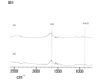
- FIG. 4 is a diagram showing FT-IR analysis results in Examples.
- FIG. 10 is a diagram showing another FT-IR analysis result in Example.
- FIG. 4 is a diagram showing XRD profiles in Examples.
- FIG. 11 shows another XRD profile in the example;
- the conductive two-dimensional particles in this embodiment are A conductive two-dimensional particle of a layered material comprising one or more layers,
- the layer has the following formula: M m X n (wherein M is at least one Group 3, 4, 5, 6, 7 metal; X is a carbon atom, a nitrogen atom, or a combination thereof; n is 1 or more and 4 or less, m is greater than n and less than or equal to 5) and a modification or termination T (T is at least one selected from the group consisting of a hydroxyl group, a fluorine atom, an oxygen atom and a hydrogen atom) present on the surface of the layer body.
- the conductive two-dimensional particles when used to form a conductive film, for example, can form a conductive film with high initial conductivity and suppressed deterioration of conductivity over time. .
- FIG. 1 is a schematic cross-sectional view illustrating interlayer cross-linking in the conductive two-dimensional particles of this embodiment.
- titanium atoms (not shown) in the layer body of MXene 10a in one layer and titanium atoms (not shown) in the layer body of MXene 10b in another layer ) are bonded via oxygen atoms 21 to form a crosslinked structure 23 between the two layers of MXene.
- FIG. 1 is a schematic cross-sectional view illustrating interlayer cross-linking in the conductive two-dimensional particles of this embodiment.
- titanium atoms (not shown) in the layer body of MXene 10a in one layer and titanium atoms (not shown) in the layer body of MXene 10b in another layer are bonded via oxygen atoms 21 to form a crosslinked structure 23 between the two layers of MXene.
- FIG. 1 is a schematic cross-sectional view illustrating interlayer cross-linking in the conductive two-dimensional particles of this embodiment.
- FIG. 1 shows a crosslinked structure between two layers of MXene for ease of explanation. It may include a crosslinked structure with other existing MXenes and a crosslinked structure between the MXene 10b in FIG. 1 and other MXenes existing below it, and may also include a case where three or more layers of MXenes are combined by a crosslinked structure.
- FIG. 1 shows a crosslinked structure between single-layer MXenes. layer MXene).
- the conductive two-dimensional particles of the present embodiment do not contain halogen atoms having a large atomic radius in the conductive two-dimensional particles, so that the distance between the MXene layer bodies and the layer bodies is shortened, and the conductive two-dimensional particles have a conductivity of 2 It is believed that the heat treatment in the manufacturing process of the dimensional particles forms many cross-links between the layer bodies of MXene. As a result, it is considered that the MXene interlayer spacing is sufficiently narrowed, the intrusion of water molecules is sufficiently suppressed, and the hygroscopic resistance is enhanced. Moreover, it is considered that the crosslinked structure is formed by a dehydration reaction of hydroxyl groups on the surface of MXene.
- a conductive film containing the conductive two-dimensional particles of the present embodiment particularly a conductive film formed of the conductive two-dimensional particles of the present embodiment, has high conductivity and can maintain high conductivity for a long period of time.
- the interlayer cross-linking is a titanium atom-oxygen atom-titanium atom (Ti-O-Ti) bond of 800 to 900 cm -1 by FT-IR (Fourier transform infrared spectroscopy). It can be determined by the presence or absence of peaks.
- MXene including one or more layers that constitute the conductive two-dimensional particles of the present embodiment will be described below.
- the layered material may be understood as a layered compound, also denoted as "M m X n T s ", where s is any number, conventionally x or z may be used instead of s.
- n can be 1, 2, 3 or 4, but is not so limited.
- M is preferably at least one selected from the group consisting of Ti, Zr, Hf, V, Nb, Ta, Cr, Mo and Mn, and from Ti, V, Cr and Mo At least one selected from the group consisting of is more preferable.
- M can be titanium or vanadium and X can be a carbon or nitrogen atom.
- MXene's precursor MAX phase is Ti 3 AlC 2 and MXene is Ti 3 C 2 Ts (in other words, M is Ti, X is C, n is 2 and m is 3).
- MXene may contain a relatively small amount of residual A atoms, for example, 10% by mass or less relative to the original A atoms.
- the residual amount of A atoms can be preferably 8% by mass or less, more preferably 6% by mass or less. However, even if the residual amount of A atoms exceeds 10% by mass, there may be no problem depending on the application and usage conditions of the electrode.
- MXene which constitutes the conductive two-dimensional particles according to the present embodiment, will be described below with reference to FIG.
- the conductive two-dimensional particles according to the present embodiment are aggregates containing crosslinked products of one layer of MXene 10c (single-layer MXene) schematically illustrated in FIG. It is an aggregate containing a plurality of cross-linked products in which MXene10c is cross-linked.
- the MXene 10c includes a layer main body (M m X n layer) 1a represented by M m X n and a surface of the layer main body 1a (more specifically, at least two surfaces facing each other in each layer).
- the MXene forming the crosslinked structure can be one layer or multiple layers.
- a multiple-layer MXene includes, but is not limited to, a two-layer MXene 10d as schematically shown in FIG. 2(b). 1b, 3b, 5b and 7b in FIG. 2(b) are the same as 1a, 3a, 5a and 7a in FIG. 2(a) described above.
- Two adjacent MXene layers (eg 7a and 7b) of a multi-layer MXene are not necessarily completely separated and may be in partial contact.
- the MXene 10c exists in one layer by separating the multilayer MXene 10d individually, and the unseparated multilayer MXene 10d remains and may be a mixture of the single layer MXene 10c and the multilayer MXene 10d. Even when the multi-layered MXene is included, the multi-layered MXene is preferably MXene with a small number of layers obtained through a delamination treatment.
- the phrase “the number of layers is small” means, for example, that the number of layers of MXene is 10 or less.
- this "multilayer MXene with a small number of layers" may be referred to as a "small layer MXene".
- the thickness of the small-layer MXene in the stacking direction is preferably 15 nm or less, more preferably 10 nm or less.
- single-layer MXene and small-layer MXene may be collectively referred to as "single-layer/small-layer MXene".
- MXenes that form the crosslinked structure are monolayer/small-layer MXenes. Since many of the MXenes forming the crosslinked structure are single-layer/small-layer MXenes, the specific surface area of the MXenes can be made larger than that of the multi-layer MXenes, and as a result, deterioration of conductivity over time can be further suppressed. .
- single-layer/small-layer MXenes with a lamination number of 10 layers or less and a thickness of 15 nm or less, preferably 10 nm or less account for 80% by volume or more of all MXenes forming a crosslinked structure.
- the volume of the monolayer MXene is larger than the volume of the few-layer MXene. Since the true densities of these MXenes do not vary greatly depending on the form of existence, it can be said that it is more preferable that the mass of single-layer MXenes is larger than the mass of small-layer MXenes. When these relationships are satisfied, the specific surface area of MXene can be increased, and deterioration of conductivity with time can be further suppressed. Most preferably, the crosslinked structure is formed only by single-layer MXene.
- each MXene layer (corresponding to the MXene layers 7a and 7b described above) can be, for example, 1 nm or more and 30 ⁇ m or less, for example, 1 nm or more and 5 nm or less, Furthermore, it may be 1 nm or more and 3 nm or less (mainly, it may vary depending on the number of M atomic layers included in each layer).
- the interlayer distance (or gap dimension, indicated by ⁇ d in FIG. 2(b)) is, for example, ⁇ 0.8 nm and ⁇ 10 nm, especially ⁇ 0.8 nm and ⁇ 5 nm. Below, more particularly about 1 nm, the total number of layers can be from 2 to 20,000.
- the conductive two-dimensional particles do not contain a chlorine atom, an iodine atom and a bromine atom (hereinafter collectively referred to as "halogen atoms"). Since the conductive two-dimensional particles do not contain halogen atoms, cross-linking between the layer bodies of MXene is likely to be formed during the production process of the conductive two-dimensional particles.
- a conductive film containing a layer body of MXene and conductive two-dimensional particles that are highly crosslinked in the layer body has better resistance to moisture absorption and exhibits high conductivity over a long period of time than a conventional crosslinked MXene film.
- the above-mentioned "not containing a chlorine atom, an iodine atom and a bromine atom” means that the content of each atom is less than the lower limit of determination when measured using an ion chromatography device, as shown in the examples described later, that is, It means less than 0.004% by mass of chlorine atoms, less than 0.04% by mass of iodine atoms, and less than 0.02% by mass of bromine atoms.
- the above contents are most preferably 0% by mass.
- the conductive two-dimensional particles have at least one selected from the group consisting of fluorine atoms, oxygen atoms, and hydroxyl groups.
- the surface of the main layer constituting MXene has at least one selected from the group consisting of fluorine atoms, oxygen atoms and hydroxyl groups.
- at least one selected from the group consisting of fluorine atoms, oxygen atoms, and hydroxyl groups with small atomic radii is present, for example, on the surface of the layer body constituting MXene, so that the interlayer distance is increased.
- the conductive two-dimensional particles may further have phosphate ions (PO 4 3 ⁇ ) on the surface.
- the phosphate ion may be derived from H 3 PO 4 (phosphoric acid), which is a raw material used in the manufacturing process of the conductive two-dimensional particles.
- H 3 PO 4 phosphoric acid
- MXene is easily formed into a monolayer, and conductive two-dimensional particles containing more single-layer and few-layer MXene can be obtained.
- a conductive film formed using conductive two-dimensional particles containing more single-layer/small-layer MXene is preferable because of its higher conductivity. Furthermore, it may contain a phosphorus atom derived from a phosphate ion.
- the conductive two-dimensional particles of the present embodiment may have a phosphorus atom content of 0.2% by mass or more and 14% by mass or less.
- the presence of phosphate ions in the conductive two-dimensional particles can be confirmed, for example, by performing high-resolution analysis (narrow scan analysis) using an X-ray photoelectron spectrometer on the binding of M in the MXene layer.
- the presence of phosphorus atoms in the conductive two-dimensional particles can be confirmed by the XPS method.
- the conductive two-dimensional particles of the present embodiment do not contain halogen atoms, dispersants, etc., and the distance between the layers constituting the MXene is shorter than that of the conventional MXene. Due to the narrow gap between layers of MXene, it is difficult for water molecules to penetrate, and it is excellent in hygroscopic resistance. The narrow gap between layers of MXene can be judged from the XRD profile obtained by X-ray diffraction measurement.
- the XRD profile obtained by X-ray diffraction measurement it can be judged by the position of the low-angle peak of 10° (deg) or less corresponding to the (002) plane of MXene. A higher angle peak in the XRD profile indicates a narrower interlayer distance.
- the peak position is more preferably 8.5° or more. Note that the upper limit of the peak position is about 9.0°.
- the peak position refers to the peak top.
- the X-ray diffraction measurement may be performed under the conditions shown in Examples described later.
- the object to be measured may be a conductive two-dimensional particle or a conductive film containing conductive two-dimensional particles.
- the method for producing conductive two-dimensional particles of the present embodiment includes: (a) the following formula: M m AX n (wherein M is at least one Group 3, 4, 5, 6, 7 metal; X is a carbon atom, a nitrogen atom, or a combination thereof; A is at least one Group 12, 13, 14, 15, 16 element; n is 1 or more and 4 or less, m is greater than n and less than or equal to 5) preparing a precursor represented by (b) etching to remove at least some of the A atoms from the precursor using an etchant that does not contain chlorine atoms, iodine atoms and bromine atoms; (c) washing the etched product obtained by etching with water to obtain a water-washed product; (d) performing an intercalation treatment of the intercalation compound, which includes stirring a mixed solution containing the water-washed product and the intercalation compound of the water-washed product; (e) performing delamination using the intercalated product obtained by the intercal
- a predetermined precursor that can be used in this embodiment is the MAX phase, which is a precursor of MXene, The formula below: M m AX n (wherein M is at least one Group 3, 4, 5, 6, 7 metal; X is a carbon atom, a nitrogen atom, or a combination thereof; A is at least one Group 12, 13, 14, 15, 16 element; n is 1 or more and 4 or less, m is greater than n and less than or equal to 5) is represented by
- A is at least one Group 12, 13, 14, 15, 16 element, usually a Group A element, typically Groups IIIA and IVA, more particularly Al, Ga, In, It may contain at least one selected from the group consisting of Tl, Si, Ge, Sn, Pb, P, As, S and Cd, preferably Al.
- a MAX phase is a crystal in which a layer composed of A atoms is located between two layers denoted by M m X n (each X may have a crystal lattice located in an octahedral array of M). have a structure.
- the MAX phase can be produced by a known method. For example, TiC powder, Ti powder and Al powder are mixed in a ball mill, and the resulting mixed powder is fired in an Ar atmosphere to obtain a fired body (block-shaped MAX phase). After that, the obtained sintered body can be pulverized with an end mill to obtain a powdery MAX phase for the next step.
- Etching is performed to remove at least a portion of A atoms from the precursor using an etchant that does not contain chlorine atoms, iodine atoms and bromine atoms.
- the etchant used in the manufacturing method of this embodiment does not contain a chlorine atom, an iodine atom, or a bromine atom. That is, it does not contain acids such as HCl, HI, HBr, or other chlorides, iodides, bromides.
- the etchant contains at least hydrofluoric acid.
- the etchant preferably further contains one or more of phosphoric acid and sulfuric acid, and more preferably further contains phosphoric acid.
- etching by a so-called MILD method in which HCl and LiF contained in an etchant are reacted in a system to generate HF, but etching is preferably performed with an etchant containing HF (hydrofluoric acid).
- a so-called ACID method or etching with an etchant further containing phosphoric acid.
- a mixture of the above acid and, for example, pure water as a solvent may be used.
- the HF concentration in the etching solution is, for example, 1.5M or more and 14M or less
- the H 3 PO 4 concentration is, for example, 5.5M or more
- the H 2 SO 4 concentration is, for example, 5.0M or more.
- An example of the etching product obtained by the above etching is slurry.
- the etched product obtained by the etching is washed with water.
- the acid and the like used in the etching can be sufficiently removed.
- the amount of water to be mixed with the etched material and the cleaning method are not particularly limited.
- water may be added, followed by stirring, centrifugation, and the like.
- Stirring methods include handshake, automatic shaker, shear mixer, pot mill, and the like.
- the degree of stirring such as stirring speed and stirring time may be adjusted according to the amount, concentration, etc. of the object to be treated.
- the washing with water may be performed once or more. Washing with water is preferably carried out multiple times.
- An intercalation treatment of the intercalation compound is performed, which includes stirring a mixture containing the water-washed material and the intercalation compound in the water-washed material.
- the compound for interlayer insertion of the treated water is not particularly limited as long as it is a compound that can be inserted between the layers of the treated water and can be separated into layers in the next step (e) delamination.
- Alkali metal compounds and alkaline earth metal compounds are preferable as the intercalation compound.
- Li-containing compounds are more preferred.
- an ionic compound in which Li ions and cations are combined can be used. Examples include hydroxides, phosphates, sulfide salts including sulfates, nitrates, acetates, and carboxylates of Li ions. Hydroxide is preferred, and lithium hydroxide is more preferred.
- the liquid properties of the mixture containing the water-washed product and the intercalating compound of the water-washed product are not limited.
- the mixture containing the water wash and the intercalating compound of the water wash is preferably alkaline.
- the pH of the mixed solution is preferably in the range of 8-14.
- the method for making the mixed solution alkaline is not limited, and a mixed solution containing a hydroxide as an intercalation compound, preferably lithium hydroxide as an Li-containing compound, or an intercalation compound and a pH adjuster.
- a mixed solution containing ammonia, potassium hydroxide, sodium hydroxide, calcium hydroxide, magnesium hydroxide and other hydroxides may be used.
- the content of the intercalation compound in the intercalation compound is preferably 0.001% by mass or more.
- the above content is more preferably 0.01% by mass or more, still more preferably 0.1% by mass or more.
- the content of the intercalation compound is preferably 10% by mass or less, more preferably 1% by mass or less.
- the specific method of intercalation is not particularly limited, and for example, the intercalation compound may be mixed with the water medium clay of MXene, stirred, or allowed to stand still.
- stirring at room temperature is mentioned.
- the stirring method include a method using a stirrer such as a stirrer, a method using a stirring blade, a method using a mixer, and a method using a centrifugal device.
- the stirring time can be set according to the manufacturing scale of the electrode, and can be set, for example, between 12 and 24 hours.
- Delamination is performed using the intercalated product obtained by intercalation.
- delamination includes a step of centrifuging the intercalated product, discarding the supernatant, and washing the remaining precipitate with water.
- Conditions for the delamination treatment are not particularly limited.
- the dispersion medium used for delamination is also not particularly limited, and for example, one or more of a polar organic dispersion medium and an aqueous dispersion medium may be used.
- polar organic dispersion medium for example, a carbonyl group, an ester group, an amide group, a formamide group, a carbamoyl group, a carbonate group, an aldehyde group, an ether group, a sulfonyl group, a sulfinyl group, a hydroxyl group, and a cyano group having a boiling point of 285° C. or less , and nitro groups.
- polar organic dispersion media include methanol (MeOH), ethanol (EtOH), dimethyl sulfoxide (DMSO), propylene carbonate (PC), N methylformamide (NMF), acetone, methyl ethyl ketone ( MEK), and one or more of tetrahydrofuran (THF), acetonitrile, N-methylacetamide (NMAc), N,N-dimethylformamide (DMF), N,N-dimethylacetamide (DMAC), sulfolane, N-methylpyrrolidone (NMP) is mentioned.
- the aqueous dispersion medium is typically water, and optionally contains a relatively small amount of other liquid substance in addition to water (for example, 30% by mass or less, preferably 20% by mass or less, based on the total amount). good.
- a polar organic dispersion medium and an aqueous dispersion medium may be stirred multiple times during delamination.
- a polar organic dispersion medium such as N-methylformamide (NMF)
- NMF N-methylformamide
- the supernatant may be centrifuged and the supernatant after centrifugation may be discarded to obtain single-layer/small-layer MXene-containing clay as a delaminated product.
- Conductive two-dimensional particles are obtained by subjecting the delaminated material obtained by the delamination to heat treatment at 200° C. or higher in an inert gas atmosphere.
- the heat treatment temperature is preferably 300° C. or higher, more preferably 400° C. or higher.
- the heat treatment temperature can be, for example, 700° C. or less.
- the heat treatment atmosphere is an inert gas atmosphere such as argon or nitrogen.
- the pressure during the heat treatment is also not particularly limited, and may be normal pressure or vacuum.
- MXene which does not contain a large steric element such as chlorine, is annealed at a high temperature without being oxidized. A crosslinked MXene with significantly improved reliability) can be realized.
- the conductive film of the present embodiment includes a conductive film (crosslinked MXene film) containing the conductive two-dimensional particles of the present embodiment.
- the conductive film of this embodiment will be described with reference to FIG. FIG. 3 illustrates a conductive film 30 obtained by stacking only conductive two-dimensional particles 100 .
- the conductive film of this embodiment is not limited to this.
- the conductive film may be a conductive composite material film (conductive composite material film) that further contains a polymer (resin).
- the polymer may be included as an additive such as a binder added during film formation, or may be added to provide strength or flexibility.
- the proportion of the polymer in the conductive composite material film (dry) can be more than 0% by volume, preferably 30% by volume or less.
- the proportion of the polymer may even be 10% by volume or less, even more 5% by volume or less.
- the proportion of the conductive two-dimensional particles (particles of the layered material) in the conductive composite film (dry) is preferably 70% by volume or more, more preferably 90% by volume or more, and even more preferably 95% by volume. It is good also as more than volume%.
- the conductive film may be a laminated film of two or more conductive composite material films having different proportions of the conductive two-dimensional particles.
- the polymer examples include a hydrophilic polymer (including a hydrophobic polymer mixed with a hydrophilic auxiliary agent to exhibit hydrophilicity, and a hydrophobic polymer whose surface has been subjected to a hydrophilic treatment).
- the polymer is one or more selected from the group consisting of polysulfone, cellulose acetate, regenerated cellulose, polyethersulfone, water-soluble polyurethane, polyvinyl alcohol, sodium alginate, acrylic acid-based water-soluble polymer, polyacrylamide, polyaniline sulfonic acid, and nylon. is more preferably included.
- the hydrophilic polymer is more preferably a hydrophilic polymer having a polar group, and the polar group is a group that forms a hydrogen bond with the modification or termination T of the layer.
- the polymer for example, one or more polymers selected from the group consisting of water-soluble polyurethane, polyvinyl alcohol, sodium alginate, acrylic acid-based water-soluble polymer, polyacrylamide, polyaniline sulfonic acid, and nylon are preferably used.
- one or more polymers selected from the group consisting of water-soluble polyurethane, polyvinyl alcohol, and sodium alginate are more preferable.
- a polymer having a urethane bond having both properties of a hydrogen bond donor and a hydrogen bond acceptor is preferable, and from that point of view, the water-soluble polyurethane is particularly preferable.
- the film thickness of the conductive film is preferably 0.5 ⁇ m or more and 20 ⁇ m or less. By increasing the film thickness of the conductive film, the contact resistance of the grain boundary is reduced and the electrical conductivity tends to be increased.
- the film thickness is more preferably 1.0 ⁇ m or more. From the viewpoint of conductivity, a thicker film thickness is more preferable, but when flexibility or the like is required, the film thickness is preferably 20 ⁇ m or less, more preferably 15 ⁇ m or less.
- the thickness of the conductive film can be measured, for example, by micrometer measurement, scanning electron microscope (SEM), microscope, laser microscope, or other cross-sectional observation.
- the conductive film of the present embodiment preferably maintains a conductivity of 5000 S/cm or more when, for example, it is in the form of a sheet with a thickness of 10 ⁇ m formed of the conductive two-dimensional particles.
- the conductivity is more preferably 5500 S/cm or higher, and more preferably 6000 S/cm or higher.
- Conductivity can be determined as follows. That is, the surface resistivity is measured by the 4-probe method, and the value obtained by multiplying the thickness [cm] by the surface resistivity [ ⁇ / ⁇ ] is the volume resistivity [ ⁇ . cm], and its reciprocal can be used to obtain the conductivity [S/cm].
- the method of manufacturing the conductive film of this embodiment using the conductive two-dimensional particles produced as described above is not particularly limited.
- a conductive film can be formed as exemplified below.
- a dispersion of conductive two-dimensional particles in which the conductive two-dimensional particles prepared as described above are present in a medium liquid examples include aqueous medium liquids and organic medium liquids.
- the medium liquid constituting the dispersion of the conductive two-dimensional particles is typically water, and in some cases, in addition to water, a relatively small amount of other liquid substance (for example, 30% by mass or less on the whole basis, preferably is 20% by mass or less).
- a dispersion of conductive two-dimensional particles may be used to form a precursor of a conductive film (also referred to as a "precursor film").
- a method for forming the precursor film is not particularly limited, and for example, suction filtration, coating, spraying, and the like can be used.
- a dispersion of conductive two-dimensional particles for example, a supernatant liquid containing conductive two-dimensional particles is appropriately adjusted (for example, diluted with an aqueous medium liquid), and a filter (conductive film It may constitute a predetermined member together with the filter, or may be finally separated from the conductive membrane) by suction filtering through the filter to at least partially remove the aqueous medium liquid.
- a precursor film can be formed thereon.
- the filter is not particularly limited, a membrane filter or the like can be used.
- the conductive film can be produced without using the binder or the like.
- a conductive film can be produced without using a binder or the like.
- the dispersion of the conductive two-dimensional particles may be applied to the base material as it is or after being appropriately adjusted (for example, diluted with an aqueous medium liquid or added with a binder).
- a coating method for example, a method of spray coating using a nozzle such as a one-fluid nozzle, a two-fluid nozzle, or an airbrush, a table coater, a comma coater, a slit coat using a bar coater, screen printing, metal mask printing, or the like. method, spin coating, dip coating, dropping, and the like.
- the base material for example, a substrate formed of a metal material, resin, or the like suitable for a biosignal sensing electrode can be appropriately employed. By coating on any suitable substrate (which may constitute a predetermined member together with the conductive film, or which may be finally separated from the conductive film), the substrate A precursor film can be formed on the material.
- drying means removing any aqueous medium liquid that may be present in the precursor.
- Drying can be done under mild conditions such as natural drying (typically placed in an air atmosphere at normal temperature and pressure) or air drying (blowing air), or hot air drying (blowing heated air). ), heat drying, and/or vacuum drying.
- the drying may be performed at a temperature of 400° C. or less using, for example, a normal pressure oven or a vacuum oven.
- the formation and drying of the precursor film may be repeated as appropriate until the desired conductive film thickness is obtained.
- the combination of spraying and drying may be repeated multiple times.
- a conductive film before cross-linking is formed by using conductive two-dimensional particles before cross-linking, and then a heat treatment is performed to obtain a conductive film. good.
- the formation of the pre-crosslinking conductive film using the pre-crosslinking two-dimensional particles and the heat treatment may be performed under the conditions described above.
- the conductive composite material of the present embodiment has a sheet-like form
- the conductive two-dimensional particles and polymer can be mixed to form a coating film, for example, as exemplified below.
- a dispersion of conductive two-dimensional particles in which the conductive two-dimensional particles are present in a medium liquid one or more of an aqueous medium liquid and an organic medium liquid
- a medium liquid one or more of an aqueous medium liquid and an organic medium liquid
- powdery conductive two-dimensional particles may be mixed with a polymer.
- the medium liquid constituting the dispersion of the conductive two-dimensional particles is typically water, and in some cases, in addition to water, a relatively small amount of other liquid substance (for example, 30% by mass or less on the whole basis, preferably is 20% by mass or less).
- the conductive two-dimensional particles and polymer can be stirred using a dispersing device such as a homogenizer, a propeller stirrer, a thin-film orbital stirrer, a planetary mixer, a mechanical shaker, or a vortex mixer.
- a dispersing device such as a homogenizer, a propeller stirrer, a thin-film orbital stirrer, a planetary mixer, a mechanical shaker, or a vortex mixer.
- the slurry which is a mixture of the conductive two-dimensional particles and the polymer, may be applied to a base material (for example, a substrate), but the application method is not limited.
- a method of spray coating using a nozzle such as a one-fluid nozzle, a two-fluid nozzle, or an airbrush
- a method of slit coating using a table coater, a comma coater, or a bar coater a method such as screen printing or metal mask printing, or spin coating.
- dip coating, and dripping for the substrate, a substrate formed of a metal material, resin, or the like suitable for a biosignal sensing electrode can be appropriately employed.
- Drying and curing may be performed at temperatures of 400° C. or less using, for example, a normal pressure oven or a vacuum oven.
- a conductive paste containing the conductive two-dimensional particles is a conductive paste containing the conductive two-dimensional particles.
- the conductive paste include a mixture of conductive two-dimensional particles and a medium.
- the medium include aqueous medium liquids, organic medium liquids, polymers, metal particles, ceramic particles, and the like, and those containing one or more of these are included.
- the mass ratio of the conductive two-dimensional particles in the conductive paste is, for example, 50% or more.
- conductive paste for example, applying it to a substrate or the like and drying it to form a conductive film can be cited as an example of application.
- Electrode 5 Conductive composite material
- Other applications using the conductive two-dimensional particles of the present embodiment include conductive composite materials containing the conductive two-dimensional particles and a polymer.
- the conductive composite material is not limited to the shape of the conductive composite material film (conductive composite film) described above.
- the shape of the conductive composite material may be a shape having thickness, a rectangular parallelepiped, a sphere, a polygon, or the like, other than the film shape.
- the same polymer as the polymer used for the conductive composite film (conductive composite film) can be used.
- it may be contained as an additive such as a binder for molding, or may be added to provide strength or flexibility.
- the proportion of the polymer in the conductive composite material (dry) is greater than 0% by volume, preferably 30% by volume or less.
- the proportion of the polymer may even be 10% by volume or less, even more 5% by volume or less.
- the ratio of the particles of the layered material in the conductive composite material (dry) is preferably 70% by volume or more, more preferably 90% by volume or more, and even more preferably 95% by volume or more.
- the polymer examples include a hydrophilic polymer (including a hydrophobic polymer mixed with a hydrophilic auxiliary agent to exhibit hydrophilicity, and a hydrophobic polymer whose surface has been subjected to a hydrophilic treatment).
- the polymer is one or more selected from the group consisting of polysulfone, cellulose acetate, regenerated cellulose, polyethersulfone, water-soluble polyurethane, polyvinyl alcohol, sodium alginate, acrylic acid-based water-soluble polymer, polyacrylamide, polyaniline sulfonic acid, and nylon. is more preferably included.
- the hydrophilic polymer is more preferably a hydrophilic polymer having a polar group, and the polar group is a group that forms a hydrogen bond with the modification or termination T of the layer.
- the polymer for example, one or more polymers selected from the group consisting of water-soluble polyurethane, polyvinyl alcohol, sodium alginate, acrylic acid-based water-soluble polymer, polyacrylamide, polyaniline sulfonic acid, and nylon are preferably used.
- one or more polymers selected from the group consisting of water-soluble polyurethane, polyvinyl alcohol, and sodium alginate are more preferable.
- a polymer having a urethane bond having both properties of a hydrogen bond donor and a hydrogen bond acceptor is preferable, and from that point of view, the water-soluble polyurethane is particularly preferable.
- the conductive two-dimensional particles, the method for producing the conductive two-dimensional particles, the conductive film, the conductive paste, and the conductive composite material in the embodiments of the present invention have been described in detail above, various modifications are possible.
- the conductive two-dimensional particles of the present disclosure may be manufactured by a method different from the manufacturing method in the above-described embodiment, and the conductive two-dimensional particle manufacturing method of the present disclosure is the same as in the above-described embodiment. Note that it is not limited to just providing conductive two-dimensional particles.
- Example 1 (1) precursor (MAX) preparation, (2) precursor etching, (3) post-etching cleaning, (4) Li intercalation, ( 5) Delamination, and (6) formation of a film using conductive two-dimensional particles before cross-linking and heat treatment were performed in this order to obtain a sample.
- the samples were obtained by performing up to the film formation.
- etching is performed under the following etching conditions to form a solid-liquid mixture (slurry) containing a solid component derived from the Ti 3 AlC 2 powder.
- Example 3 interlayer cross-linking of titanium atom-oxygen atom-titanium atom (Ti--O--Ti) was confirmed. On the other hand, in Comparative Examples 3, 6 and 7, the interlayer cross-linking could not be confirmed. Further, in Comparative Examples 3, 6 and 7, a hydroxyl group peak was clearly confirmed, but in Example 3, a hydroxyl group peak was not confirmed. From these facts, it is considered that in Example 3, interlayer cross-linking bonds of titanium atom-oxygen atom-titanium atom (Ti--O--Ti) were formed due to the dehydration reaction of hydroxyl groups on the MXene surface.
Landscapes
- Chemical & Material Sciences (AREA)
- Organic Chemistry (AREA)
- Chemical Kinetics & Catalysis (AREA)
- Inorganic Chemistry (AREA)
- Health & Medical Sciences (AREA)
- Medicinal Chemistry (AREA)
- Polymers & Plastics (AREA)
- Physics & Mathematics (AREA)
- Dispersion Chemistry (AREA)
- Spectroscopy & Molecular Physics (AREA)
- Laminated Bodies (AREA)
Priority Applications (3)
| Application Number | Priority Date | Filing Date | Title |
|---|---|---|---|
| JP2023550424A JP7708195B2 (ja) | 2021-09-30 | 2022-08-05 | 導電性2次元粒子およびその製造方法 |
| CN202280065525.6A CN118043914A (zh) | 2021-09-30 | 2022-08-05 | 导电性二维粒子及其制造方法 |
| US18/616,605 US20240239663A1 (en) | 2021-09-30 | 2024-03-26 | Conductive two-dimensional particle and method for producing the same |
Applications Claiming Priority (2)
| Application Number | Priority Date | Filing Date | Title |
|---|---|---|---|
| JP2021161527 | 2021-09-30 | ||
| JP2021-161527 | 2021-09-30 |
Related Child Applications (1)
| Application Number | Title | Priority Date | Filing Date |
|---|---|---|---|
| US18/616,605 Continuation US20240239663A1 (en) | 2021-09-30 | 2024-03-26 | Conductive two-dimensional particle and method for producing the same |
Publications (1)
| Publication Number | Publication Date |
|---|---|
| WO2023053721A1 true WO2023053721A1 (ja) | 2023-04-06 |
Family
ID=85782288
Family Applications (1)
| Application Number | Title | Priority Date | Filing Date |
|---|---|---|---|
| PCT/JP2022/030048 Ceased WO2023053721A1 (ja) | 2021-09-30 | 2022-08-05 | 導電性2次元粒子およびその製造方法 |
Country Status (4)
| Country | Link |
|---|---|
| US (1) | US20240239663A1 (https=) |
| JP (1) | JP7708195B2 (https=) |
| CN (1) | CN118043914A (https=) |
| WO (1) | WO2023053721A1 (https=) |
Cited By (1)
| Publication number | Priority date | Publication date | Assignee | Title |
|---|---|---|---|---|
| WO2025182741A1 (ja) * | 2024-02-29 | 2025-09-04 | 株式会社村田製作所 | 2次元粒子、2次元粒子含有膜、および2次元粒子含有分散液 |
Citations (2)
| Publication number | Priority date | Publication date | Assignee | Title |
|---|---|---|---|---|
| WO2021025026A1 (ja) * | 2019-08-05 | 2021-02-11 | 株式会社村田製作所 | 導電性材料、導電性フィルム、電気化学キャパシタ、導電性材料の製造方法および導電性フィルムの製造方法 |
| WO2021131643A1 (ja) * | 2019-12-25 | 2021-07-01 | 株式会社村田製作所 | 導電性複合構造体およびその製造方法 |
-
2022
- 2022-08-05 JP JP2023550424A patent/JP7708195B2/ja active Active
- 2022-08-05 WO PCT/JP2022/030048 patent/WO2023053721A1/ja not_active Ceased
- 2022-08-05 CN CN202280065525.6A patent/CN118043914A/zh active Pending
-
2024
- 2024-03-26 US US18/616,605 patent/US20240239663A1/en active Pending
Patent Citations (2)
| Publication number | Priority date | Publication date | Assignee | Title |
|---|---|---|---|---|
| WO2021025026A1 (ja) * | 2019-08-05 | 2021-02-11 | 株式会社村田製作所 | 導電性材料、導電性フィルム、電気化学キャパシタ、導電性材料の製造方法および導電性フィルムの製造方法 |
| WO2021131643A1 (ja) * | 2019-12-25 | 2021-07-01 | 株式会社村田製作所 | 導電性複合構造体およびその製造方法 |
Cited By (1)
| Publication number | Priority date | Publication date | Assignee | Title |
|---|---|---|---|---|
| WO2025182741A1 (ja) * | 2024-02-29 | 2025-09-04 | 株式会社村田製作所 | 2次元粒子、2次元粒子含有膜、および2次元粒子含有分散液 |
Also Published As
| Publication number | Publication date |
|---|---|
| JPWO2023053721A1 (https=) | 2023-04-06 |
| US20240239663A1 (en) | 2024-07-18 |
| CN118043914A (zh) | 2024-05-14 |
| JP7708195B2 (ja) | 2025-07-15 |
Similar Documents
| Publication | Publication Date | Title |
|---|---|---|
| JP7513110B2 (ja) | 導電性2次元粒子およびその製造方法、導電性膜、導電性複合材料、ならびに導電性ペースト | |
| Kim et al. | Fabrication of flexible reduced graphene oxide–TiO 2 freestanding films for supercapacitor application | |
| JP7501645B2 (ja) | 導電性2次元粒子およびその製造方法 | |
| JP6152924B1 (ja) | グラフェン分散液およびその製造方法、グラフェン−活物質複合体粒子の製造方法ならびに電極ペーストの製造方法 | |
| Park et al. | Highly dispersible edge-selectively oxidized graphene with improved electrical performance | |
| JP7487783B2 (ja) | 導電性2次元粒子およびその製造方法 | |
| KR20140002682A (ko) | 그래핀 분말, 이의 제조 방법 및 이를 포함하는 전기 화학 소자 | |
| JP7670151B2 (ja) | 導電性2次元粒子含有組成物、導電性膜、および導電性2次元粒子含有組成物の製造方法 | |
| US20240239663A1 (en) | Conductive two-dimensional particle and method for producing the same | |
| WO2023048081A1 (ja) | 2次元粒子、導電性膜、導電性ペーストおよび2次元粒子の製造方法 | |
| WO2020129427A1 (ja) | グラファイトの薄板状構造物の製造方法、並びに、薄片化グラファイトおよびその製造方法 | |
| US20250388740A1 (en) | Two-dimensional particle-containing composition and production method for two-dimensional particle-containing composition | |
| US20250161977A1 (en) | Film and method for producing same | |
| Duong et al. | Amphiphilic silane-MXene hybrids for high-performance flexible symmetric supercapacitors via additive-free processing | |
| CN113555217A (zh) | 一种碳纳米管/石墨烯/聚偏氟乙烯介电复合材料及其制备方法 | |
| US20240279069A1 (en) | Two-dimensional particle, conductive film, conductive paste, and method for producing two-dimensional particle | |
| WO2023162423A1 (ja) | 2次元粒子、2次元粒子の製造方法および材料 | |
| WO2023127376A1 (ja) | セラミックス材料、セラミックス材料の製造方法、2次元粒子の製造方法および物品の製造方法 | |
| JP7537613B2 (ja) | 磁性材料、電磁気部品及び磁性材料の製造方法 | |
| WO2023223780A1 (ja) | 導電性2次元粒子およびその製造方法、導電性膜、導電性ペースト、ならびに導電性複合材料 | |
| WO2025182741A1 (ja) | 2次元粒子、2次元粒子含有膜、および2次元粒子含有分散液 | |
| WO2025225525A1 (ja) | 導電性粒子、フィルム、ペースト、コンポジット材料、および導電性粒子の製造方法 | |
| WO2024203470A1 (ja) | 2次元粒子、導電性膜およびその製造方法 | |
| CN121779752A (zh) | 高熵陶瓷/聚合物复合电介质薄膜及其制备方法、应用 | |
| WO2023233783A1 (ja) | 電極および電極の製造方法 |
Legal Events
| Date | Code | Title | Description |
|---|---|---|---|
| 121 | Ep: the epo has been informed by wipo that ep was designated in this application |
Ref document number: 22875597 Country of ref document: EP Kind code of ref document: A1 |
|
| WWE | Wipo information: entry into national phase |
Ref document number: 2023550424 Country of ref document: JP |
|
| WWE | Wipo information: entry into national phase |
Ref document number: 202280065525.6 Country of ref document: CN |
|
| NENP | Non-entry into the national phase |
Ref country code: DE |
|
| 122 | Ep: pct application non-entry in european phase |
Ref document number: 22875597 Country of ref document: EP Kind code of ref document: A1 |