WO2023053437A1 - イオンミリング装置 - Google Patents
イオンミリング装置 Download PDFInfo
- Publication number
- WO2023053437A1 WO2023053437A1 PCT/JP2021/036376 JP2021036376W WO2023053437A1 WO 2023053437 A1 WO2023053437 A1 WO 2023053437A1 JP 2021036376 W JP2021036376 W JP 2021036376W WO 2023053437 A1 WO2023053437 A1 WO 2023053437A1
- Authority
- WO
- WIPO (PCT)
- Prior art keywords
- rod
- ion
- source
- electrode
- ion source
- Prior art date
Links
- 238000000992 sputter etching Methods 0.000 title claims abstract description 46
- 150000002500 ions Chemical class 0.000 claims abstract description 120
- 230000001133 acceleration Effects 0.000 claims description 32
- 238000010884 ion-beam technique Methods 0.000 claims description 27
- 238000011084 recovery Methods 0.000 claims description 5
- XKRFYHLGVUSROY-UHFFFAOYSA-N Argon Chemical compound [Ar] XKRFYHLGVUSROY-UHFFFAOYSA-N 0.000 description 23
- 239000007789 gas Substances 0.000 description 18
- 229910052786 argon Inorganic materials 0.000 description 15
- 238000010586 diagram Methods 0.000 description 12
- -1 argon ions Chemical class 0.000 description 7
- 238000000034 method Methods 0.000 description 7
- 238000004544 sputter deposition Methods 0.000 description 5
- 238000000151 deposition Methods 0.000 description 3
- 230000008021 deposition Effects 0.000 description 3
- 239000002245 particle Substances 0.000 description 3
- 230000005856 abnormality Effects 0.000 description 2
- 230000005540 biological transmission Effects 0.000 description 2
- 238000001514 detection method Methods 0.000 description 2
- 238000002347 injection Methods 0.000 description 2
- 239000007924 injection Substances 0.000 description 2
- 230000007774 longterm Effects 0.000 description 2
- 230000002093 peripheral effect Effects 0.000 description 2
- 238000005498 polishing Methods 0.000 description 2
- 230000001681 protective effect Effects 0.000 description 2
- 239000004065 semiconductor Substances 0.000 description 2
- 230000002411 adverse Effects 0.000 description 1
- 239000000919 ceramic Substances 0.000 description 1
- 239000011521 glass Substances 0.000 description 1
- 238000004519 manufacturing process Methods 0.000 description 1
- 239000000463 material Substances 0.000 description 1
- 239000002184 metal Substances 0.000 description 1
- 238000003801 milling Methods 0.000 description 1
- 239000000203 mixture Substances 0.000 description 1
- 238000004886 process control Methods 0.000 description 1
- 239000011347 resin Substances 0.000 description 1
- 229920005989 resin Polymers 0.000 description 1
Images


Classifications
-
- H—ELECTRICITY
- H01—ELECTRIC ELEMENTS
- H01J—ELECTRIC DISCHARGE TUBES OR DISCHARGE LAMPS
- H01J37/00—Discharge tubes with provision for introducing objects or material to be exposed to the discharge, e.g. for the purpose of examination or processing thereof
- H01J37/02—Details
- H01J37/04—Arrangements of electrodes and associated parts for generating or controlling the discharge, e.g. electron-optical arrangement, ion-optical arrangement
- H01J37/08—Ion sources; Ion guns
-
- H—ELECTRICITY
- H01—ELECTRIC ELEMENTS
- H01J—ELECTRIC DISCHARGE TUBES OR DISCHARGE LAMPS
- H01J37/00—Discharge tubes with provision for introducing objects or material to be exposed to the discharge, e.g. for the purpose of examination or processing thereof
- H01J37/30—Electron-beam or ion-beam tubes for localised treatment of objects
- H01J37/305—Electron-beam or ion-beam tubes for localised treatment of objects for casting, melting, evaporating or etching
Definitions
- the present invention relates to an ion milling device.
- An ion milling apparatus irradiates an unfocused ion beam onto a sample (e.g., metal, semiconductor, glass, ceramic, etc.) to be observed with an electron microscope, and spatters atoms on the surface of the sample without stress by a sputtering phenomenon. It is used for polishing the sample surface and exposing the internal structure of the sample.
- the sample surface polished by the ion beam and the exposed internal structure of the sample are used for observation with a scanning electron microscope or a transmission electron microscope.
- a high voltage is applied between the anode and cathode inside the ion source to ionize the introduced gas with generated electrons, and an acceleration voltage is applied to extract the ions from the ion source and irradiate the sample.
- the cathode is worn by the sputtering phenomenon caused by the generated plasma, and a conductive deposited film derived from the composition of the cathode is formed on the inner wall surface of the anode.
- the deposited film grows with the lapse of operating time of the apparatus.
- the deposited film that has grown exfoliates like a needle and short-circuits between the anode and the cathode, making it impossible to generate ions. Therefore, it was necessary to disassemble the ion source and remove the short circuit. For this reason, in the conventional ion milling apparatus, it was necessary to interrupt sample processing and remove the deposited film every time a short circuit occurred.
- Cited Document 1 it is possible to remove the deposited film without decomposing the ion source by using the gas injection means. Pulling is required and processing efficiency is reduced.
- An ion milling apparatus which is an embodiment of the present invention, comprises a sample chamber, a sample stage disposed in the sample chamber on which the sample is placed, a first internal electrode, a second internal electrode, and an acceleration electrode. a source, a rod-shaped electrode that can be inserted into and removed from the ion source, and a power supply unit connected to the first internal electrode, the second internal electrode, the acceleration electrode, and the rod-shaped electrode, With the rod-shaped electrode retracted from the ion source, the power supply unit applies a first discharge voltage between the first internal electrode and the second internal electrode, and accelerates the voltage between the first internal electrode and the acceleration electrode.
- the ion source accelerates ions generated by collisions between the gas and electrons generated by the discharge between the first internal electrode and the second internal electrode, and accelerates them into the sample. emits as an unfocused beam of ions directed towards With the rod-shaped electrode inserted into the ion source, the power supply unit applies a second discharge voltage between the rod-shaped electrode and the first internal electrode and the second internal electrode, thereby causing the ion source to move inside. , ions are generated by collision of electrons generated by discharge between the rod-like electrode and the first internal electrode or the second internal electrode with the gas.
- An ion milling apparatus which is another embodiment of the present invention, includes a sample chamber, a sample stage disposed in the sample chamber on which the sample is placed, and electrons generated by discharge between an anode and a cathode.
- an ion source that accelerates ions with an acceleration electrode to emit them as an unfocused ion beam toward a sample;
- a power supply unit that is connected to the anode, the cathode, and the acceleration electrode;
- the discharge voltage applied between the anode and the cathode to the power supply unit and the difference between the anode and the accelerating electrode.
- a control unit stops application of an acceleration voltage applied between them, inserts a rod-shaped member into the ion source, and removes a short-circuited portion between the anode and the cathode with a brush.
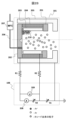
- FIG. 1 is a schematic diagram showing the main parts of an ion milling apparatus of Example 1.
- FIG. FIG. 4 is a diagram showing possible positional relationships between a shutter and an ion source;
- FIG. 4 is a diagram showing possible positional relationships between a shutter and an ion source;
- FIG. 2 is a schematic diagram showing an ion source and a power supply circuit that applies a control voltage to internal electrodes of the ion source;
- FIG. 2 is a schematic diagram showing an ion source and a power supply circuit that applies a control voltage to internal electrodes of the ion source; It is a schematic diagram which shows a mode that the shaft was inserted in the ion source.
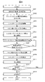
- FIG. 4 is a flow chart showing a series of operations from the start to end of sample processing of the ion milling apparatus of Example 1.
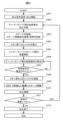
- FIG. FIG. 5 is a schematic diagram showing the main part of the ion milling apparatus of Example 2; 9 is a flow chart showing a series of operations from the start to end of sample processing of the ion milling apparatus of Example 2.
- FIG. 10 is a schematic diagram showing how a shaft with a brush is inserted into the ion source in the ion milling apparatus of Example 3; This is the shaft rotation source viewed from the Y direction. 10 is a flow chart showing a series of operations from the start to end of sample processing of the ion milling apparatus of Example 3.
- FIG. 5 is a schematic diagram showing the main part of the ion milling apparatus of Example 2; 9 is a flow chart showing a series of operations from the start to end of sample processing of the ion milling apparatus of Example 2.
- FIG. 10 is a schematic diagram showing how a shaft with a brush is
- a shutter 104 is provided in front of the ion source 101 to block irradiation of the sample with the ion beam.
- the direction in which the ion beam is emitted is called the front of the ion source, which corresponds to the Y direction in the example of FIG. 1A.
- a shutter drive source 105 drives the shutter 104 .
- FIGS. 1B shows a state in which the shaft 106 is retracted from the ion source 101 and the shutter 104 blocks the ion beam emitted from the ion source 101.
- FIG. FIG. 1C shows a state in which the shutter 104 is retracted from the front of the ion source 101 and the sample can be milled by the ion beam.
- FIG. 2A is a schematic diagram showing the ion source 101 adopting the Penning method and a power supply circuit that applies a control voltage to the internal electrodes of the ion source 101.
- the power supply circuit is part of the power supply unit 108 .
- the power supply circuit is equipped with an ammeter 208 and a voltmeter 209 between the anode 203 and the first cathode 201 and the second cathode 202 .
- the ammeter 208 measures the discharge current flowing between the cathode and the anode due to discharge
- the voltmeter 209 measures the discharge voltage actually applied between the cathode and the anode during discharge.
- a discharge current value measured by the ammeter 208 and a discharge voltage value measured by the voltmeter 209 are also output to the control unit 109 .
- the control unit 109 may use the discharge current value and the discharge voltage value to monitor the output state of the ion beam and display them on the display unit 110 .
- FIG. 2B shows the ion source 101 with the anode-cathode shorted. This short circuit eliminates the potential difference between the anode and the cathode and stops the discharge, thereby interrupting sample processing.
- FIG. 3 is a schematic diagram showing how the shaft 106 is inserted into the ion source 101 in order to remove the short circuit after the anode-cathode short circuit shown in FIG. 2B.
- the control unit 109 detects occurrence of a short circuit between the anode and the cathode, for example, when the discharge voltage value measured by the voltmeter 209 drops abnormally. Upon detection of the occurrence of the short circuit, the control unit 109 stops applying the control voltage to the ion source 101, moves the shutter 104 by the shutter drive source 105, and arranges the shaft 106 coaxially with the opening 211 of the acceleration electrode 205. do.
- the power supply unit 108 applies a high voltage (second discharge voltage) between the shaft 106 and the short-circuited cathodes 201, 202 and anode 203, thereby turning the ion source on.
- Argon gas introduced into 101 is ionized.
- the voltage Ve is a voltage value of negative polarity with respect to the reference potential
- the discharge voltage Vd and the acceleration voltage Va are set to 0 V so that a high voltage (second 2 discharge voltage) is applied and a discharge occurs.
- the shaft 106 functions as an anode
- the cathodes 201, 202 and 203 function as cathodes.
- the control unit 109 drives the shutter drive source 105 to move the shaft 106 forward of the ion source 101. At this time, the shaft 106 and the ion source 101 are arranged coaxially.
- the control unit 109 drives the shutter driving source 105 to retract the shaft 106 from the front of the ion source 101.
- step S311 If the anode-cathode short circuit occurs again during sample processing, the process returns to step S302 to remove the anode-cathode short circuit.
- FIG. 6 shows a series of operations from the start to end of sample processing of the ion milling apparatus 100B of the second embodiment.
- the same steps as those in the flowchart (FIG. 4) of the first embodiment are denoted by the same reference numerals, and overlapping descriptions are omitted.
- the control unit 109 drives the sample stage drive source 103 so that the shaft 106 and the ion source 101 are arranged coaxially. This operation changes the position and attitude of the sample stage 102 from the state before the interruption of processing. Therefore, the state information of the sample stage before being driven by the sample stage drive source 103 is recorded (S303').
- the state information is information for recovering the sample stage 102 to the state before the interruption of processing after short-circuit recovery, and includes the position coordinates (x, y, z) of the sample stage 102 and, if necessary, the posture of the sample stage 102. It contains information (tilt ⁇ 1 about T 1 axis, tilt ⁇ 2 about T 2 axis).
- FIG. 7A is a schematic diagram showing the ion source 101 of the ion milling apparatus of Example 3 and a power supply circuit that applies a control voltage to the internal electrodes of the ion source 101.
- FIG. The difference from Examples 1 and 2 is the method of removing the short-circuited portion between the anode and the cathode.
- a brush 401 is provided at the tip of a shaft (rod-shaped member) 106 , and the shaft 106 is attached to a shaft rotation source 402 via a shaft drive source 107 .
- the shaft 106 in Example 3 does not function as an external electrode and functions as a support member for the brush 401 .
- the shaft rotation source 402 viewed from the Y direction is shown in FIG. 7B.
- the shaft rotation source 402 rotates around the rotation center CC, and the shaft 106 rotates as the shaft rotation source 402 rotates.
- the shaft rotation source 402 is configured such that the holding positions of the shaft 106 and the shaft drive source 107 can be moved from the rotation center CC in the outer peripheral direction of the shaft rotation source 402 .
- Example 3 the controller 109 may stop the supply of argon gas to the ion source 101 .
- the control unit 109 drives the shutter drive source 105 to move the shaft 106 forward of the ion source 101 (S303).
- the shaft 106 is positioned at the rotation center CC of the shaft rotation source 402 so that the rotation center CC of the shaft rotation source 402 is arranged on the central axis of the ion source 101 .
- the shaft 106 and the ion source 101 are arranged coaxially.
Landscapes
- Chemical & Material Sciences (AREA)
- Analytical Chemistry (AREA)
- Physics & Mathematics (AREA)
- Engineering & Computer Science (AREA)
- Plasma & Fusion (AREA)
- Sampling And Sample Adjustment (AREA)
Abstract
アノード-カソード間が短絡し、試料加工が中断された場合でも、試料加工に自動復帰できるイオンミリング装置を提供する。イオンミリング装置は、試料室(111)と、試料室内に配置され、試料を載置する試料ステージ(102)と、第1の内部電極(203)、第2の内部電極(202)を備えるイオン源(101)と、イオン源に挿抜可能な棒状電極(106)と、第1の内部電極(203)、第2の内部電極(202)及び棒状電極(106)に接続される電源ユニット(108)とを有し、棒状電極(106)がイオン源(101)に挿入された状態で、電源ユニット(108)は棒状電極(106)と第1の内部電極(203)及び第2の内部電極(202)との間に第2の放電電圧を印加することにより、イオン源(101)はその内部に、棒状電極(106)と第1の内部電極(203)または第2の内部電極(202)との間の放電により発生した電子とガスとの衝突によりイオンを発生させる。
Description
本発明は、イオンミリング装置に関する。
イオンミリング装置は、電子顕微鏡観察対象である試料(例えば、金属、半導体、ガラス、セラミックなど)に対して非集束のイオンビームを照射し、スパッタリング現象によって試料表面の原子を無応力で弾き飛ばし、試料表面の研磨や試料の内部構造を露出させるために使用する。イオンビームによって研磨された試料表面や露出された試料の内部構造は、走査電子顕微鏡や透過電子顕微鏡の観察に用いられる。
特許文献1は、イオンミリング装置にイオンガンに向けてガスを噴射するガス噴射手段を設け、イオンガン内部に付着した付着物を移動させることを開示している。
イオンミリング装置では、イオン源内部のアノード-カソード間に高電圧を印加して、発生した電子で導入したガスをイオン化し、加速電圧を印加してイオンをイオン源から引き出し、試料に照射する。このときイオン源内部では、生成したプラズマによるスパッタリング現象でカソードが摩耗し、カソード組成由来の導電性を有する堆積膜がアノード内壁面に形成される。堆積膜は装置稼働時間経過に伴い成長する。成長した堆積膜は針状に剥離してアノード-カソード間を短絡させることにより、イオンを生成することができなくなる。このため、イオン源を分解して短絡箇所を除去する必要があった。このため、従来のイオンミリング装置では短絡が生じるたびに、試料加工を中断して堆積膜を除去する必要があった。
引用文献1では、ガス噴射手段を用いることでイオン源を分解することなく、堆積膜を除去することを可能にしているが、試料室を一旦大気開放して、短絡復帰後再度試料室の真空引きが必要であり、加工効率が低下する。
半導体製造プロセスにおける工程管理のため、イオンミリング装置を工場のライン内に配置し、電子顕微鏡によって観察する試料の表面研磨や内部構造を露出させる加工をすることを想定する場合、イオンミリング装置は多数の試料を連続して自動で加工を行うことが望まれる。多数の試料を連続して自動でミリング加工するには、長時間の連続したイオンビーム照射を伴う。このため、アノード-カソード間に短絡が生じても、自動的に短絡を除去し、短時間のうちに加工処理に復帰することが可能なイオンミリング装置が望まれる。
本発明の一実施の態様であるイオンミリング装置は、試料室と、試料室内に配置され、試料を載置する試料ステージと、第1の内部電極、第2の内部電極及び加速電極を備えるイオン源と、イオン源に挿抜可能な棒状電極と、第1の内部電極、第2の内部電極、加速電極及び棒状電極に接続される電源ユニットとを有し、
棒状電極がイオン源から退避された状態で、電源ユニットは第1の内部電極と第2の内部電極との間に第1の放電電圧を、第1の内部電極と加速電極との間に加速電圧を印加することにより、イオン源は第1の内部電極と第2の内部電極との間の放電により発生した電子とガスとの衝突により生成されるイオンを加速電圧により加速して、試料に向かう非集束のイオンビームとして放出し、
棒状電極がイオン源に挿入された状態で、電源ユニットは棒状電極と第1の内部電極及び第2の内部電極との間に第2の放電電圧を印加することにより、イオン源はその内部に、棒状電極と第1の内部電極または第2の内部電極との間の放電により発生した電子とガスとの衝突によりイオンを発生させる。
本発明の別の実施の態様であるイオンミリング装置は、試料室と、試料室内に配置され、試料を載置する試料ステージと、アノードとカソードとの間の放電により発生した電子によって生成されたイオンを加速電極により加速することにより、試料に向かう非集束のイオンビームとして放出するイオン源と、アノード、カソード及び加速電極に接続される電源ユニットと、イオン源に挿抜可能であって、先端にブラシが設けられた棒状部材と、イオンビームによる試料の加工中にアノードとカソードとの短絡を検知したとき、電源ユニットにアノードとカソードとの間に印加される放電電圧とアノードと加速電極との間に印加される加速電圧の印加を停止させ、イオン源に棒状部材を挿入し、ブラシによりアノードとカソードとの短絡箇所を除去させる制御部とを有する。
アノード-カソード間が短絡し、試料加工が中断された場合でも、試料加工に自動復帰できるイオンミリング装置を提供する。これにより、長時間の連続した試料加工を自動化できる。
その他の課題と新規な特徴は、本明細書の記述および添付図面から明らかになるであろう。
以下、本発明の実施例を図面に基づいて説明する。
図1Aは、実施例1のイオンミリング装置100の主要部を側面から示した模式図である。図1Aでは、鉛直方向をZ方向として表示している。イオンミリング装置100は、その主要な構成として、イオン源101、試料ステージ102、試料ステージ駆動源103、シャッター104、シャッター駆動源105、外部電極として機能し、イオン源101に挿抜可能なシャフト(棒状電極)106、シャフト駆動源107、電源ユニット108、制御部109、表示部110、試料室111を有する。
イオンミリング装置100は、走査電子顕微鏡や透過電子顕微鏡によって試料の表面あるいは断面を観察するための前処理装置として用いられる。このような前処理装置向けのイオン源は、構造を小型化するために有効なペニング方式を採用する場合が多い。本実施例でもイオン源101はペニング方式を採用しており、イオン源101から試料ステージ102に設置された試料に向けて、非集束のイオンビームが照射される。イオンビームの出力は、主に、電源ユニット108がイオン源101の内部電極に印加する制御電圧(加速電圧、放電電圧)やイオン源101に供給されるアルゴンガスの流量によって制御される。
試料が載置される試料ステージ102は、試料ステージ102の位置決めを行う試料ステージ駆動源103を介して試料室111に取付けられている。試料ステージ駆動源103は回転軸R0を中心に試料ステージ102を回転させる。また、試料ステージ駆動源103は、試料ステージ102の位置をX方向、Y方向、Z方向のそれぞれに、また、イオンビーム中心軸B0に対する試料ステージ102の向きをXZ平面の角度方向(T1軸を中心とする回転方向)、YZ平面の角度方向(T2軸を中心とする回転方向)のそれぞれに調整可能なように、試料室111に取付けられている。
イオン源101の前方には、イオンビームの試料への照射を遮断するシャッター104が設けられている。ここでは、イオンビームが射出される方向をイオン源の前方と呼んでおり、図1Aの例ではY方向にあたる。シャッター104はシャッター駆動源105により駆動される。シャッター104はZ方向に移動可能に構成されるものとして、図1B~Cにシャッター104とイオン源101とがとりうる位置関係を示す。図1Bはシャフト106をイオン源101から退避させ、かつシャッター104がイオン源101から放出されるイオンビームを遮断している状態である。図1Cはシャッター104をイオン源101の前方から退避させ、イオンビームによる試料のミリング加工が可能とされた状態である。
この例では、シャッター104にシャフト駆動源107を設け、シャッター駆動源105を、シャッター104と連動してシャフト106のZ方向の位置を移動させる駆動源として共用することで、シャッター駆動源105、シャフト駆動源107の駆動状況にかかわらず、シャフト106はイオンビーム中心軸B0と同一YZ平面内に位置することになり、機構が簡素化されている。なお、以上は一例であり、図1A~Cに示した機構に限定するものではない。例えば、シャッター104の退避方向はZ方向でなくてもよく、シャフト106をシャッター104とは独立に駆動させるための専用の駆動源を設けてもよい。
本実施例のイオンミリング装置による試料加工は次のように行われる。イオン源101からのイオンビームの電流値があらかじめ設定した範囲で安定するまで、シャッター104により、不安定なイオンビームの試料への照射を遮断する。このときのシャッター104は図1Bに示す位置にある。イオンビーム電流値が安定した後は、シャッター駆動源105によりシャッター104がイオン源101の前方から退避させられる(図1C)ことにより、試料ステージ102上の試料にイオンビーム照射が開始される。
試料加工中にイオン源101内部で短絡が発生すると、シャッター駆動源105によりイオン源101とシャフト106とが同軸上に配置されるようシャフト106の位置を移動させる。イオン源101とシャフト106とが同軸上に配置されると、シャフト駆動源107は、シャフト106をY方向に移動させて、イオン源101内部に挿入する。このときのシャッター104、シャフト106の状態が図1Aの状態である。詳細は後述するが、短絡箇所を除去するため、電源ユニット108は、イオン源101内部に挿入されたシャフト106とイオン源101の内部電極との間に高電圧を印加する。
以上の制御は、制御部109によって行われ、短絡発生や短絡復帰などイオン源101の状況は表示部110からリアルタイムで確認できるようになっている。
図2Aは、ペニング方式を採用したイオン源101とイオン源101の内部電極に制御電圧を印加する電源回路とを示す模式図である。電源回路は電源ユニット108の一部である。
イオン源101は、第1カソード201、第2カソード(第2の内部電極)202、アノード(第1の内部電極)203、永久磁石204、加速電極205、ガス配管206を有する。ガス配管206にはイオン源101に供給するアルゴンガスの流量を制御するマスフローコントローラ207が設けられている。
イオン源101内部には、第1カソード201と第2カソード202とが永久磁石204を介して電圧印加時に同電位となるように配置されている。第1カソード201と第2カソード202の間にアノード203が配置されている。カソード201,202とアノード203との間に電源ユニット108から放電電圧Vd(第1の放電電圧)が印加されることにより電子が発生する。永久磁石204によってイオン源101内部で電子は螺旋運動を行いながら滞留し、ガス配管206から注入されたアルゴンガスと衝突してアルゴンイオンを生成する。アノード203と加速電極205との間には電源ユニット108から加速電圧Vaが印加されており、生成されたアルゴンイオンは加速電極205に誘引され、イオンビームとして放出される。加速電極205は基準電位(GND)とされており、カソード201,202とアノード203にそれぞれ制御電圧を与えるための電位が電源ユニット108から供給されている。ここで、カソードとアノードに印加される電位が急激に変動することにより、イオン源101の動作に悪影響を及ぼすのを防止するため、それぞれ保護抵抗R1,R2が設けられている。保護抵抗の代わりに異常発生時に電圧の印加を遮断する保護回路を設けてもよい。
電源回路にはアノード203と第1カソード201及び第2カソード202との間に電流計208及び電圧計209が備えられている。電流計208により放電によりカソードとアノードとの間に流れる放電電流が測定され、電圧計209により放電中にカソードとアノードとの間に実際に印加されている放電電圧が測定される。電流計208により測定される放電電流値、電圧計209により測定される放電電圧値も制御部109に出力される。制御部109は放電電流値、放電電圧値をイオンビームの出力状態をモニタリングするために使用し、それらを表示部110に表示してもよい。
アルゴンイオンを生成するための放電を繰り返すうちに、第2カソード202はアルゴンイオンによってスパッタリングされることによって摩耗していく。摩耗により発生するカソード由来のスパッタリング粒子がアノード内壁面に堆積することにより堆積膜210が形成され、堆積膜210はやがて針状に剥離して、アノード-カソード間を短絡させる。図2Bにアノード-カソード間が短絡されたイオン源101を示す。この短絡によりアノード-カソード間の電位差がなくなり、放電が停止することによって試料加工が中断される。
図3は、図2Bに示したアノード-カソード間での短絡発生後に、短絡箇所を除去するため、イオン源101にシャフト106を挿入した様子を示した模式図である。制御部109は、例えば、電圧計209により測定される放電電圧値が異常低下することで、アノード-カソード間の短絡発生を検知する。短絡発生の検知を受けて、制御部109はイオン源101への制御電圧の印加を停止するとともに、シャッター駆動源105によってシャッター104を動かし、シャフト106を加速電極205の開口211と同軸上に配置する。同軸上に配置するのは、制御誤差等によりシャフト106がイオン源101の内部電極と接触することを防止するためである。その後、シャフト駆動源107によって、イオン源101の内部にシャフト106を挿入する。電源ユニット108は、シャフト106と加速電極205との間に電圧Veを印加する電源回路を有している。シャフト106に印加される電圧が急激に変動する可能性を考慮し、保護抵抗R3が設けられている。保護抵抗R3の代わりに異常発生時に電圧の印加を遮断する保護回路を設けてもよい。
シャフト106がイオン源101に挿入された後、電源ユニット108がシャフト106と短絡されたカソード201,202及びアノード203との間に高電圧(第2の放電電圧)を印加することにより、イオン源101内に導入されたアルゴンガスがイオン化される。ここで、電圧Veは基準電位に対して負の極性の電圧値とし、放電電圧Vd及び加速電圧Vaを0Vとすることで短絡されたカソード201,202及びアノード203との間に高電圧(第2の放電電圧)が印加され、放電が生じる。このとき、シャフト106がアノード、カソード201,202及びアノード203がカソードとして機能することになる。実施の態様の記述においては、イオンビーム放出時の機能を元に内部電極をカソード201,202及びアノード203と呼称して、記述を単純化している。なお、第2の放電電圧を負電圧Veと正電圧Vaの和として放電を生じさせてもよい。
アルゴンイオンが堆積膜210をスパッタリング現象で削ることにより、アノード-カソード間の短絡から復帰する。短絡の復帰は、電源ユニット108がアノード-カソード間に所定の電圧を印加した場合に、電圧計209に印加した電圧が表れることで判定できる。短絡復帰が検知されると、制御部109は、イオン源101からシャフト106を退避させる。
図4に示すフローチャートに、実施例1のイオンミリング装置100の試料加工開始から終了までの一連の動作を示す。試料加工中における短絡検知から加工再開までの処理は、制御部109により自動的に実施される。以下に、各ステップでの動作について説明する。
S301:イオンミリング装置100の試料加工条件を設定し、試料加工を開始する。試料加工条件には、イオン源101の加速電圧、放電電圧、アルゴンガスの供給量、試料ステージの位置、試料加工時間等が含まれる。
S302:試料加工中、制御部109は電流計208により放電電流値、電圧計209により放電電圧値をモニタしている。制御部109は、電圧計209で測定される放電電圧値からアノード-カソード間の短絡を検知すると、電源ユニット108からの放電電圧Vd、加速電圧Vaの印加を停止し、試料加工を中断する。このとき制御部109は、イオン源101へのアルゴンガスの供給は継続する。
S303:制御部109は、シャッター駆動源105を駆動させ、シャフト106をイオン源101前方に移動させる。このとき、シャフト106とイオン源101とが同軸上に配置されるようにする。
S304:制御部109は、シャフト駆動源107を駆動させ、シャフト106をイオン源101に挿入する。
S305:短絡したアノード203およびカソード201,202とシャフト106との間に電圧Veを印加することにより、シャフトとアノード及びカソードとの間で放電させる。これにより、イオン源101に導入されたアルゴンガスがイオン化される。
S306:発生させたアルゴンイオンによるスパッタリング現象により、アノード-カソード間の短絡箇所を除去する。
S307:一定時間、シャフト106へ電圧Veを印加した後、アノード203とカソード201,202との間に所定の電圧を印加し、アノード-カソード間の短絡箇所が除去されたことを確認する。短絡箇所が除去されたかどうかは、印加した電圧に応じた電位差がアノード-カソード間で電圧計209によって測定されるかによって判定できる。短絡箇所が除去されていない場合には引き続きステップS306を実行する。
S308:アノード-カソード間の短絡復帰後、制御部109は、電源ユニット108からのシャフト106への電圧印加を停止し、シャフト駆動源107を駆動させ、イオン源101からシャフト106を退避させる。
S309:制御部109は、シャッター駆動源105を駆動させ、シャフト106をイオン源101前方から退避させる。
S310:ステップS301で設定した試料加工条件により、中断した試料加工を再開する。
S311:試料加工中にアノード-カソード間の短絡が再発した場合、ステップS302に戻ってアノード-カソード間の短絡除去動作を行う。
S312:ステップS301で設定した試料加工時間到達により、試料加工を終了する。
図5は、実施例2のイオンミリング装置100Bの主要部を側面から示した模式図である。イオンミリング装置100Bでは、シャッター104ではなく、試料ステージ102にシャフト106を設けている。実施例1と同様の機能をもつ構成については同じ符号を付して、重複する説明は省略する。シャフト106をY方向に移動させるシャフト駆動源107は試料ステージ102に設けられる。これにより、シャフト駆動源107を実装するにあたり、試料ステージ102を駆動する試料ステージ駆動源103の駆動機構を共用し、機構を簡素化することが可能になる。
実施例1と異なる点は、イオン源101内部で短絡が発生したときのシャフト106の挿入の過程である。実施例2ではシャフト106が試料ステージ102に設けられているため、シャフト106をイオン源101に挿入するために試料ステージ102の位置及び姿勢が変化する。このため、短絡発生時の試料ステージの位置情報及び姿勢(傾斜)情報を記憶してから、シャフト106のイオン源101への挿入動作を行い、短絡除去後に、記憶した試料ステージの位置情報及び姿勢情報に基づき、試料ステージ102の位置及び姿勢を短絡除去動作前の状態に復帰させる。
図6に示すフローチャートに、実施例2のイオンミリング装置100Bの試料加工開始から終了までの一連の動作を示す。実施例1のフローチャート(図4)と同じステップについては同じ符号を付して、重複する説明については省略する。
アノード-カソード間の短絡発生による加工中断(S302)後、制御部109は、シャフト106とイオン源101とが同軸に配置されるよう、試料ステージ駆動源103を駆動する。この動作によって、試料ステージ102の位置や姿勢が加工中断前の状態から変化する。そのため、試料ステージ駆動源103の駆動前の試料ステージの状態情報を記録する(S303’)。状態情報とは、短絡復帰後に試料ステージ102を加工中断前の状態に回復するための情報であって、試料ステージ102の位置座標(x,y,z)や必要に応じて試料ステージ102の姿勢情報(T1軸を中心とする傾きθ1、T2軸を中心とする傾きθ2)を含む。
試料ステージ102駆動後、実施例1と同様にシャフト駆動源107によりシャフト106をイオン源101に挿入し、アノード-カソード間の短絡箇所を除去する。短絡復帰後はイオン源101からシャフト106を退避させ(S308)、ステップS303’で記録しておいた状態情報に基づき、試料ステージ102を加工中断時の状態に復帰させる(S309’)。具体的には、制御部109は、記録された位置座標(x,y,z)に試料ステージ102を移動させ、記録された姿勢情報にしたがって試料ステージ102を傾斜させるよう、試料ステージ駆動源103を駆動する。
図7Aは、実施例3のイオンミリング装置のイオン源101とイオン源101の内部電極に制御電圧を印加する電源回路とを示す模式図である。実施例1、2とは、アノード-カソード間の短絡箇所の除去方法が異なる。
シャフト(棒状部材)106の先端にはブラシ401が設けられ、シャフト106はシャフト駆動源107を介してシャフト回転源402に取り付けられている。実施例3におけるシャフト106は、実施例1におけるシャフト106と異なり、外部電極としての機能を有さず、ブラシ401の支持部材として機能する。Y方向からみたシャフト回転源402を図7Bに示す。シャフト回転源402は回転中心CCを中心に回転し、シャフト回転源402の回転に伴ってシャフト106も回転する。シャフト回転源402は、シャフト106及びシャフト駆動源107の保持位置を、回転中心CCからシャフト回転源402の外周方向に移動可能に構成されている。シャフト回転源402は、回転中心CCからΔrだけ保持位置を外周方向に偏心させる。このとき、図7Aに示されるように、ブラシ401が第2カソード202およびアノード203の内壁面に接した状態になる。この状態で、シャフト回転源402が回転中心CCを中心としてシャフト106を回転させることにより、ブラシ401が第2カソード202およびアノード203の内壁面を沿うように回転し、スパッタ粒子の堆積膜を除去する。
ここで、ブラシ401は、接触する第2カソード202やアノード203を傷つけないよう、樹脂やゴムのような剛性が小さい材質を用い、外側に広がった部分を備えた形状(L字型)としている。L字型とすることによって、シャフト106が回転されるときに到達可能なブラシ401の最外周を、シャフト106が回転する領域よりも外側とすることができる。これにより、シャフト106を加速電極205に接触させることなく、ブラシ401をアノード203の内壁面に接触させることができる。図7AではL字型のブラシを示しているが、シャフト106が加速電極205に接触することなく、ブラシ401がアノード203の内壁面に接触できれば形状はL字型に限定されない。また、図7Aの例では、実施例1と同様にシャフト回転源402をシャッター104に設ける例を示しているが、実施例2と同様に試料ステージ102にシャフト回転源402を設けるようにしてもよい。
図8に示すフローチャートに、実施例3のイオンミリング装置の試料加工開始から終了までの一連の動作を示す。実施例1のフローチャート(図4)または実施例2のフローチャート(図6)と同じステップについては同じ符号を付して、重複する説明については省略する。
アノード-カソード間の短絡発生を検知すると加工を中断する(S302)。実施例3では、制御部109は、イオン源101へのアルゴンガスの供給を停止させてもよい。その後、制御部109は、シャッター駆動源105を駆動させ、シャフト106をイオン源101前方に移動させる(S303)。このとき、シャフト106はシャフト回転源402の回転中心CCに位置し、シャフト回転源402の回転中心CCがイオン源101の中心軸上に配置されるようにする。これにより、シャフト106とイオン源101とは同軸上に配置されることになる。
この状態で、制御部109は、シャフト駆動源107を駆動させ、シャフト106をブラシ401が第2カソード202に接触するまでイオン源101に挿入した後、シャフト回転源402のシャフト106の保持位置をブラシ401がアノード203に接触するまで(Δr)偏心させる(S304’)。偏心されたシャフト106の中心軸を図7A,Bにおいて中心軸CSとして表している。その後、制御部109は、シャフト回転源402によって回転中心CCを軸としてシャフト106を回転させることによって、ブラシ401が第2カソード202およびアノード203の内壁面を沿うように回転し、スパッタ粒子の堆積膜を除去する(S306’)。あらかじめ設定された一定時間、ブラシ401を回転させた後、アノード-カソード間の短絡箇所が除去されたことを確認する(S307)。前記イオン源から前記シャフトを退避させる。アノード-カソード間の短絡復帰後、制御部109は、シャフト駆動源107を駆動させ、イオン源101からシャフト106を退避させる(S308’)。
以上、本発明者によってなされた発明を実施の形態に基づき具体的に説明したが、本発明は記述した実施の形態に限定されるものではなく、その要旨を逸脱しない範囲で種々変更可能である。例えば、実施例1において外部電極として使用したシャフトは、アルゴンイオンによるスパッタリング現象を短絡箇所だけで効率よく引き起こすために、イオン源101に挿入されたシャフトの先端だけに電圧が印加されるように絶縁体を含めた構造としてもよい。
100,100B:イオンミリング装置、101:イオン源、102:試料ステージ、103:試料ステージ駆動源、104:シャッター、105:シャッター駆動源、106:シャフト、107:シャフト駆動源、108:電源ユニット、109:制御部、110:表示部、111:試料室、201:第1カソード、202:第2カソード、203:アノード、204:永久磁石、205:加速電極、206:ガス配管、207:マスフローコントローラ、208:電流計、209:電圧計、210:堆積膜、211:開口、401:ブラシ、402:シャフト回転源。
Claims (15)
- 試料室と、
前記試料室内に配置され、試料を載置する試料ステージと、
第1の内部電極、第2の内部電極及び加速電極を備えるイオン源と、
前記イオン源に挿抜可能な棒状電極と、
前記第1の内部電極、前記第2の内部電極、前記加速電極及び前記棒状電極に接続される電源ユニットとを有し、
前記棒状電極が前記イオン源から退避された状態で、前記電源ユニットは前記第1の内部電極と前記第2の内部電極との間に第1の放電電圧を、前記第1の内部電極と前記加速電極との間に加速電圧を印加することにより、前記イオン源は前記第1の内部電極と前記第2の内部電極との間の放電により発生した電子とガスとの衝突により生成されるイオンを前記加速電圧により加速して、前記試料に向かう非集束のイオンビームとして放出し、
前記棒状電極が前記イオン源に挿入された状態で、前記電源ユニットは前記棒状電極と前記第1の内部電極及び前記第2の内部電極との間に第2の放電電圧を印加することにより、前記イオン源はその内部に、前記棒状電極と前記第1の内部電極または前記第2の内部電極との間の放電により発生した電子とガスとの衝突によりイオンを発生させるイオンミリング装置。 - 請求項1において、
前記イオンビームによる前記試料の加工中に前記第1の内部電極と前記第2の内部電極との短絡を検知したとき、前記電源ユニットに前記第1の放電電圧と前記加速電圧の印加を停止させ、前記イオン源に前記棒状電極を挿入した後、前記電源ユニットに前記第2の放電電圧を印加させる制御部を有するイオンミリング装置。 - 請求項2において、
前記制御部は、前記電源ユニットによる前記第1の放電電圧と前記加速電圧の印加の停止後も、前記イオン源への前記ガスの供給を継続するイオンミリング装置。 - 請求項3において、
前記制御部は、前記第1の内部電極と前記第2の内部電極との短絡箇所の除去を検知したとき、前記電源ユニットに前記第2の放電電圧の印加を停止させ、前記イオン源から前記棒状電極を退避させた後、前記電源ユニットに前記第1の放電電圧と前記加速電圧の印加を再開させるイオンミリング装置。 - 請求項3において、
前記電源ユニットは、前記第1の内部電極と前記第2の内部電極との間の電位差を計測する電圧計を備え、
前記制御部は、前記電圧計が測定する電位差に基づき前記第1の内部電極と前記第2の内部電極との短絡または短絡復帰を検知するイオンミリング装置。 - 請求項4において、
前記棒状電極を前記イオン源が前記イオンビームを放出する開口の前方に移動させる第1の駆動源と、前記開口の前方に移動された前記棒状電極を前記イオン源に挿入する第2の駆動源とを有し、
前記制御部は前記第1の駆動源及び前記第2の駆動源により前記棒状電極の挿抜を行うイオンミリング装置。 - 請求項6において、
前記イオンビームの前記試料への照射を遮断するシャッターと、
前記シャッターを駆動するシャッター駆動源とを有し、
前記第1の駆動源は前記シャッター駆動源と共用されるイオンミリング装置。 - 請求項6において、
前記試料ステージの位置決めを行う試料ステージ駆動源を有し、
前記第1の駆動源は前記試料ステージ駆動源と共用されるイオンミリング装置。 - 請求項8において、
前記制御部は、前記イオン源に前記棒状電極を挿入する動作を開始する前の前記試料ステージの状態情報を記憶し、前記イオン源から前記棒状電極を退避させた後、前記状態情報に基づき前記試料ステージを前記イオン源に前記棒状電極を挿入する動作を開始する前の状態に回復させるイオンミリング装置。 - 請求項9において、
前記状態情報は、前記試料ステージの位置座標と姿勢情報を含むイオンミリング装置。 - 試料室と、
前記試料室内に配置され、試料を載置する試料ステージと、
アノードとカソードとの間の放電により発生した電子によって生成されたイオンを加速電極により加速することにより、前記試料に向かう非集束のイオンビームとして放出するイオン源と、
前記アノード、前記カソード及び前記加速電極に接続される電源ユニットと、
前記イオン源に挿抜可能であって、先端にブラシが設けられた棒状部材と、
前記イオンビームによる前記試料の加工中に前記アノードと前記カソードとの短絡を検知したとき、前記電源ユニットに前記アノードと前記カソードとの間に印加される放電電圧と前記アノードと前記加速電極との間に印加される加速電圧の印加を停止させ、前記イオン源に前記棒状部材を挿入し、前記ブラシにより前記アノードと前記カソードとの短絡箇所を除去させる制御部とを有するイオンミリング装置。 - 請求項11において、
前記制御部は、前記アノードと前記カソードとの短絡箇所の除去を検知したとき、前記イオン源から前記棒状部材を退避させた後、前記電源ユニットに前記放電電圧と前記加速電圧の印加を再開させるイオンミリング装置。 - 請求項12において、
前記棒状部材を前記イオン源が前記イオンビームを放出する開口の前方に移動させる第1の駆動源と、前記開口の前方に移動された前記棒状部材を前記イオン源に挿入する第2の駆動源と、前記棒状部材を保持し、回転中心を中心として前記棒状部材を回転させる回転源とを有し、
前記制御部は前記回転源の前記回転中心で前記棒状部材を保持した状態で、前記第1の駆動源及び前記第2の駆動源により前記棒状部材が前記カソードに接触するまで前記イオン源に挿入するイオンミリング装置。 - 請求項13において、
前記棒状部材の前記回転中心は前記イオン源の中心軸上に配置され、
前記制御部は、前記棒状部材が前記イオン源に挿入された後、前記回転源による前記棒状部材の保持位置を前記ブラシが前記カソードに接触するまで偏心させ、前記回転源により、前記回転中心を軸として前記棒状部材を回転させるイオンミリング装置。 - 請求項14において、
前記ブラシは、前記棒状部材よりも外側に広がった部分を備えた形状を有するイオンミリング装置。
Priority Applications (2)
| Application Number | Priority Date | Filing Date | Title |
|---|---|---|---|
| PCT/JP2021/036376 WO2023053437A1 (ja) | 2021-10-01 | 2021-10-01 | イオンミリング装置 |
| KR1020247010458A KR20240046301A (ko) | 2021-10-01 | 2021-10-01 | 이온 밀링 장치 |
Applications Claiming Priority (1)
| Application Number | Priority Date | Filing Date | Title |
|---|---|---|---|
| PCT/JP2021/036376 WO2023053437A1 (ja) | 2021-10-01 | 2021-10-01 | イオンミリング装置 |
Publications (1)
| Publication Number | Publication Date |
|---|---|
| WO2023053437A1 true WO2023053437A1 (ja) | 2023-04-06 |
Family
ID=85782043
Family Applications (1)
| Application Number | Title | Priority Date | Filing Date |
|---|---|---|---|
| PCT/JP2021/036376 WO2023053437A1 (ja) | 2021-10-01 | 2021-10-01 | イオンミリング装置 |
Country Status (2)
| Country | Link |
|---|---|
| KR (1) | KR20240046301A (ja) |
| WO (1) | WO2023053437A1 (ja) |
Citations (5)
| Publication number | Priority date | Publication date | Assignee | Title |
|---|---|---|---|---|
| JPH02148647A (ja) * | 1988-11-30 | 1990-06-07 | Nec Yamagata Ltd | イオン注入装置のイオンソース洗浄治具及び洗浄方法 |
| JPH0364462A (ja) * | 1989-07-31 | 1991-03-19 | Matsushita Electric Ind Co Ltd | イオンソースハウジング内壁のクリーニング方法およびクリーニング用治具 |
| CN202142496U (zh) * | 2011-07-25 | 2012-02-08 | 中芯国际集成电路制造(上海)有限公司 | 离子注入机的分析器 |
| WO2016189614A1 (ja) * | 2015-05-25 | 2016-12-01 | 株式会社日立ハイテクノロジーズ | イオンミリング装置、及びイオンミリング方法 |
| CN210207978U (zh) * | 2019-06-17 | 2020-03-31 | 德淮半导体有限公司 | 清洁装置及离子植入设备 |
-
2021
- 2021-10-01 WO PCT/JP2021/036376 patent/WO2023053437A1/ja active Application Filing
- 2021-10-01 KR KR1020247010458A patent/KR20240046301A/ko unknown
Patent Citations (5)
| Publication number | Priority date | Publication date | Assignee | Title |
|---|---|---|---|---|
| JPH02148647A (ja) * | 1988-11-30 | 1990-06-07 | Nec Yamagata Ltd | イオン注入装置のイオンソース洗浄治具及び洗浄方法 |
| JPH0364462A (ja) * | 1989-07-31 | 1991-03-19 | Matsushita Electric Ind Co Ltd | イオンソースハウジング内壁のクリーニング方法およびクリーニング用治具 |
| CN202142496U (zh) * | 2011-07-25 | 2012-02-08 | 中芯国际集成电路制造(上海)有限公司 | 离子注入机的分析器 |
| WO2016189614A1 (ja) * | 2015-05-25 | 2016-12-01 | 株式会社日立ハイテクノロジーズ | イオンミリング装置、及びイオンミリング方法 |
| CN210207978U (zh) * | 2019-06-17 | 2020-03-31 | 德淮半导体有限公司 | 清洁装置及离子植入设备 |
Also Published As
| Publication number | Publication date |
|---|---|
| KR20240046301A (ko) | 2024-04-08 |
Similar Documents
| Publication | Publication Date | Title |
|---|---|---|
| US20200328062A1 (en) | Deposition method and deposition apparatus | |
| JP6499754B2 (ja) | イオンミリング装置、及びイオンミリング方法 | |
| JP2006351374A (ja) | イオン源 | |
| WO2023053437A1 (ja) | イオンミリング装置 | |
| EP2267181B1 (en) | Target exchange type plasma generator | |
| JP2008209312A (ja) | 二次イオン質量分析装置及びその使用方法 | |
| JP4827235B2 (ja) | アーク式蒸発源及び成膜体の製造方法 | |
| US10699876B2 (en) | Method of cleaning electrostatic chuck | |
| US6610987B2 (en) | Apparatus and method of ion beam processing | |
| US20160247667A1 (en) | Sputtering apparatus | |
| JP2007149861A (ja) | イオンミリング装置 | |
| JP2019218598A (ja) | 真空アーク蒸着装置および真空アーク蒸着方法 | |
| JP2000251751A (ja) | 液体金属イオン源、および、液体金属イオン源のフローインピーダンス測定方法 | |
| JP4774322B2 (ja) | 表面処理装置 | |
| JP2008038197A (ja) | プラズマ成膜装置 | |
| JP2010003596A (ja) | 荷電粒子線加工装置 | |
| JP2006117978A (ja) | 物品処理装置 | |
| JP2006161063A (ja) | 表面処理装置及び光学素子成形用型 | |
| WO2022249371A1 (ja) | イオンミリング装置 | |
| BRPI0910613B1 (pt) | Método para manufaturar peças de trabalho e aparelho de gravura por íon | |
| TWI821868B (zh) | 離子銑削裝置 | |
| JP7332169B2 (ja) | 磁化プラズモイド射出装置 | |
| JP7104898B2 (ja) | イオン源およびそのクリーニング方法 | |
| RU2642237C2 (ru) | Плазменно-дуговое устройство формирования покрытий | |
| JPH06325711A (ja) | スパッタ型イオン源 |
Legal Events
| Date | Code | Title | Description |
|---|---|---|---|
| 121 | Ep: the epo has been informed by wipo that ep was designated in this application |
Ref document number: 21959471 Country of ref document: EP Kind code of ref document: A1 |
|
| ENP | Entry into the national phase |
Ref document number: 20247010458 Country of ref document: KR Kind code of ref document: A |
|
| WWE | Wipo information: entry into national phase |
Ref document number: 2023550993 Country of ref document: JP |